To learn more about ON Semiconductor, please visit our website at www.onsemi.com Please note: As part of the Fairchild Semiconductor integration, some of the Fairchild orderable part numbers will need to change in order to meet ON Semiconductor’s system requirements. Since the ON Semiconductor product management systems do not have the ability to manage part nomenclature that utilizes an underscore (_), the underscore (_) in the Fairchild part numbers will be changed to a dash (-). This document may contain device numbers with an underscore (_). Please check the ON Semiconductor website to verify the updated device numbers. The most current and up-to-date ordering information can be found at www.onsemi.com. Please email any questions regarding the system integration to [email protected]. Is Now Part of ON Semiconductor and the ON Semiconductor logo are trademarks of Semiconductor Components Industries, LLC dba ON Semiconductor or its subsidiaries in the United States and/or other countries. ON Semiconductor owns the rights to a number of patents, trademarks, copyrights, trade secrets, and other intellectual property. A listing of ON Semiconductor’s product/patent coverage may be accessed at www.onsemi.com/site/pdf/Patent-Marking.pdf. ON Semiconductor reserves the right to make changes without further notice to any products herein. ON Semiconductor makes no warranty, representation or guarantee regarding the suitability of its products for any particular purpose, nor does ON Semiconductor assume any liability arising out of the application or use of any product or circuit, and specifically disclaims any and all liability, including without limitation special, consequential or incidental damages. Buyer is responsible for its products and applications using ON Semiconductor products, including compliance with all laws, regulations and safety requirements or standards, regardless of any support or applications information provided by ON Semiconductor. “Typical” parameters which may be provided in ON Semiconductor data sheets and/or specifications can and do vary in different applications and actual performance may vary over time. All operating parameters, including “Typicals” must be validated for each customer application by customer’s technical experts. ON Semiconductor does not convey any license under its patent rights nor the rights of others. ON Semiconductor products are not designed, intended, or authorized for use as a critical component in life support systems or any FDA Class 3 medical devices or medical devices with a same or similar classification in a foreign jurisdiction or any devices intended for implantation in the human body. Should Buyer purchase or use ON Semiconductor products for any such unintended or unauthorized application, Buyer shall indemnify and hold ON Semiconductor and its officers, employees, subsidiaries, affiliates, and distributors harmless against all claims, costs, damages, and expenses, and reasonable attorney fees arising out of, directly or indirectly, any claim of personal injury or death associated with such unintended or unauthorized use, even if such claim alleges that ON Semiconductor was negligent regarding the design or manufacture of the part. ON Semiconductor is an Equal Opportunity/Affirmative Action Employer. This literature is subject to all applicable copyright laws and is not for resale in any manner.

Welcome message from author
This document is posted to help you gain knowledge. Please leave a comment to let me know what you think about it! Share it to your friends and learn new things together.
Transcript

To learn more about ON Semiconductor, please visit our website at www.onsemi.com
Please note: As part of the Fairchild Semiconductor integration, some of the Fairchild orderable part numbers will need to change in order to meet ON Semiconductor’s system requirements. Since the ON Semiconductor product management systems do not have the ability to manage part nomenclature that utilizes an underscore (_), the underscore (_) in the Fairchild part numbers will be changed to a dash (-). This document may contain device numbers with an underscore (_). Please check the ON Semiconductor website to verify the updated device numbers. The most current and up-to-date ordering information can be found at www.onsemi.com. Please email any questions regarding the system integration to [email protected].
Is Now Part of
ON Semiconductor and the ON Semiconductor logo are trademarks of Semiconductor Components Industries, LLC dba ON Semiconductor or its subsidiaries in the United States and/or other countries. ON Semiconductor owns the rights to a number of patents, trademarks, copyrights, trade secrets, and other intellectual property. A listing of ON Semiconductor’s product/patent coverage may be accessed at www.onsemi.com/site/pdf/Patent-Marking.pdf. ON Semiconductor reserves the right to make changes without further notice to any products herein. ON Semiconductor makes no warranty, representation or guarantee regarding the suitability of its products for any particular purpose, nor does ON Semiconductor assume any liability arising out of the application or use of any product or circuit, and specifically disclaims any and all liability, including without limitation special, consequential or incidental damages. Buyer is responsible for its products and applications using ON Semiconductor products, including compliance with all laws, regulations and safety requirements or standards, regardless of any support or applications information provided by ON Semiconductor. “Typical” parameters which may be provided in ON Semiconductor data sheets and/or specifications can and do vary in different applications and actual performance may vary over time. All operating parameters, including “Typicals” must be validated for each customer application by customer’s technical experts. ON Semiconductor does not convey any license under its patent rights nor the rights of others. ON Semiconductor products are not designed, intended, or authorized for use as a critical component in life support systems or any FDA Class 3 medical devices or medical devices with a same or similar classification in a foreign jurisdiction or any devices intended for implantation in the human body. Should Buyer purchase or use ON Semiconductor products for any such unintended or unauthorized application, Buyer shall indemnify and hold ON Semiconductor and its officers, employees, subsidiaries, affiliates, and distributors harmless against all claims, costs, damages, and expenses, and reasonable attorney fees arising out of, directly or indirectly, any claim of personal injury or death associated with such unintended or unauthorized use, even if such claim alleges that ON Semiconductor was negligent regarding the design or manufacture of the part. ON Semiconductor is an Equal Opportunity/Affirmative Action Employer. This literature is subject to all applicable copyright laws and is not for resale in any manner.
September 2015
© 2011 Fairchild Semiconductor Corporation www.fairchildsemi.com FAN4800AU/CU • Rev. 1.4
FA
N4
80
0A
U/C
U —
PF
C/ P
WM
Co
ntro
ller C
om
bin
atio
n
FAN4800AU / FAN4800CU PFC/ PWM Controller Combination
Features
Pin-to-Pin Compatible with ML4800, FAN4800, CM6800, and CM6800A
PWM Configurable for Current-Mode or Feed-Forward Voltage-Mode Operation
Internally Synchronized Leading-Edge PFC and Trailing-Edge PWM in One IC
Low Operating Current
Innovative Switching-Charge Multiplier Divider
Average-Current-Mode for Input-Current Shaping
PFC Over-Voltage and Under-Voltage Protections
PFC Feedback Open-Loop Protection
Cycle-by-Cycle Current Limiting for PFC/PWM
Power-on Sequence Control and Soft-Start
Line Sagging Protection
fRTCT=4•fPFC=4•fPWM for FAN4800AU
fRTCT=4•fPFC=2•fPWM for FAN4800CU
Applications
Desktop PC Power Supply
Internet Server Power Supply
LCD TV/ Monitor Power Supply
UPS
Battery Charger
DC Motor Power Supply
Monitor Power Supply
Telecom System Power Supply
Distributed Power
Related Resources
AN-8027 — FAN480X PFC+PWM Combination Controller Application
Description
The highly integrated FAN4800AU/CU parts are specially designed for power supplies that consist of boost PFC and PWM. They require very few external components to achieve versatile protections and compensation. They are available in 16-pin DIP and SOP packages.
The PWM can be used in current or Voltage Mode. In Voltage Mode, feed-forward from the PFC output bus can reduce secondary output ripple.
To evaluate FAN4800AU/CU for replacing existing FAN4800A/C, FAN4800AS/CS, old version FAN4800 and ML4800 boards, six things must be completed before the fine-tuning procedure:
1. Change RAC resistor from the old value to a higher
resistor value: 6 M to 8 M.
2. Change RT/CT pin from the existing values to
RT=6.8 k and CT=1000 pF to have fPFC=64 kHz and fPWM=64 kHz.
3. The VRMS pin needs to be 1.224 V at VIN=85 VAC for universal input application with line input from 85 VAC to 270 VAC.
4. Change ISENSE pin filter from the exiting values to
RFilter=51 and CFilter=0.01 µF for higher bandwidth.
5. At full load, the average VVEA must be ~4.5 V and ripple on VVEA needs to be less than 400 mV.
6. For the SS pin, the soft-start current has been reduced to half the FAN4800 capacitor.
There are two differences from FAN4800AS/CS to FAN4800AU/CU:
Add Line Sagging Protection
Fix Inductance Current Instability during AC Cycle Drop Test
FA
N4
80
0A
U/C
U —
PF
C/ P
WM
Co
ntro
ller C
om
bin
atio
n
© 2011 Fairchild Semiconductor Corporation www.fairchildsemi.com FAN4800AU/CU • Rev. 1.4
Ordering Information
Part Number Operating
Temperature Range
PFC:PWM Frequency
Ratio Package
Packing Method
FAN4800AUN
-40°C to +105°C
1:1 16-Pin Dual Inline Package (DIP) Tube
FAN4800CUN 1:2
FAN4800AUM 1:1 16-Pin Small Outline Package (SOP) Tape & Reel
FAN4800CUM 1:2
Block Diagram
VDD
15 12 OPFC
6
5
1
11 OPWM
2
16
FBPFC
2.5V/2.75V
0.5V
-1.3VISENSE
0.3V
VEA
VDD
27V/28V
1mA
ZERO POWER
PFC OVP
VDD OVP
S
R
Q
Q
S
R
Q
Q
300µA
Gain Modulator
x2
k
5.7KΩ
PFC SAW
Dead-Time
2.5V
VRMS
1.9V
1.05VDebounce 1ms
S
R
Q
Q
Debounce 30ms0.85V
VRMS
VIN OFFBOP
BI
BOP
3
10µA
10V
300Ω
UVLOVIN OFF
Level Shift 1.5V
S
R
Q
Q
FBPFC
2.4V
1.3V
BI
VIN OFF
VIN OK
S
R
Q
Q1VBlanking
PWM Max. Duty
VDD
VDD
7.5V
REFERENCE
UVLO
11V/9V
PFC UVP
PFC ILIMIT
PWM ILIMIT
VIN UVLO
ILIMIT
IAC
FBPFC
VEA
ISENSE
IEA
FBPWM
SS
AC UVLO
GMi
GMv
10 GND
10µA
13
9
4VRMS
7
PWM Max. Duty
Dead-Time
PFC SAWRT/CT
8
300Ω
PWM Max. Duty
14 VREF
RAMP
33µA
VDD
Figure 1. Function Block Diagram
© 2011 Fairchild Semiconductor Corporation www.fairchildsemi.com FAN4800AU/CU • Rev. 1.4 3
FA
N4
80
0A
U/C
U —
PF
C/ P
WM
Co
ntro
ller C
om
bin
atio
n
Application Diagrams
AC
IEA
ILIMIT
FBPWM
SS
ISENSE
IAC
GND
OPFC
VDD
FBPFC
VEA
VDD
OPWM
LBoost
CBulk
DBoost
RSENSE
RFilter
12V
5V
FBPWM
RFB1
RD
CFB
1nF
FBPWM
CFilter
CVIN
10Ω
10KΩ
Q1RFBPFC1
RFBPFC2
RFBPFC3CFBPFC
10Ω
10KΩ
10KΩ
Q2
Q3
DF1
DF2
RIEA
CIEA1
CIEA2
RVEA
CVEA1
CVEA2
CSS
RILIMIT
RFilter
CFilter
CVDD
Lm
RFB2
RFB3
10Ω
VREF
47nF VRMS
RT/CT
RAMP
RFB4
3MΩ
3MΩ
1MΩ
1MΩ
200KΩ
36KΩ220nF
RFBPWM
RRAMP
CRAMP
RT
CT
12V
5V
Figure 2. Current Mode
AC
IEA
ILIMIT
FBPWM
SS
ISENSE
IAC
GND
OPFC
VDD
FBPFC
VEA
VDD
OPWM
LBoost
CBulk
DBoost
RSENSE
RFilter
12V
5V
FBPWM
RFB1
RD
CFB
1nF
FBPWM
CFilter
CVin
10Ω
10KΩ
Q1RFBPFC1
RFBPFC2
RFBPFC3CFBPFC
10Ω
10KΩ
10KΩ
Q2
Q3
DF1
DF2
RIEA
CIEA1
CIEA2
RVEA
CVEA1
CVEA2
CSS
RILIMIT
RFilter
CFilter
CVDD
Lm
RFB2
RFB3
10Ω
VREF
47nF VRMS
RT/CT
RAMP
RFB4
3MΩ
3MΩ
1MΩ
1MΩ
200KΩ
36KΩ220nF
RFBPWM
RRAMP
CRAMP
RT
CT
12V
5V
Figure 3. Voltage Mode
© 2011 Fairchild Semiconductor Corporation www.fairchildsemi.com FAN4800AU/CU • Rev. 1.4 4
FA
N4
80
0A
U/C
U —
PF
C/ P
WM
Co
ntro
ller C
om
bin
atio
n
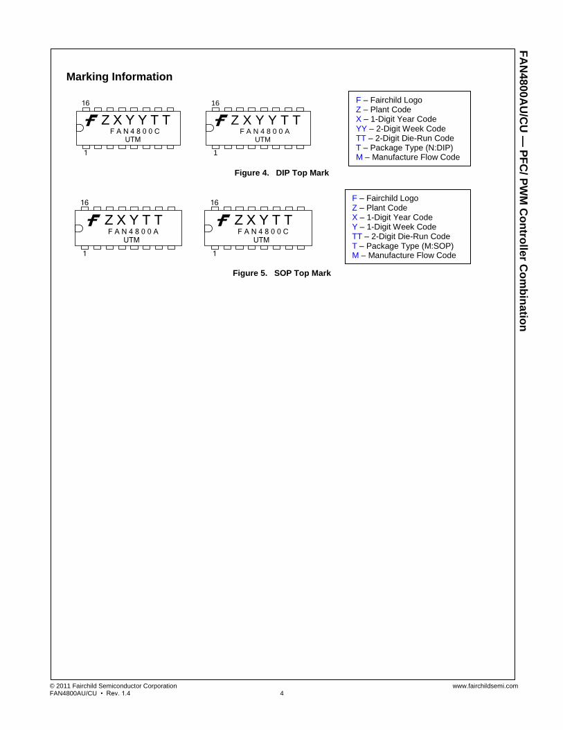
Marking Information
1
16
Z X Y Y T TF A N 4 8 0 0 C
UTM
1
16
Z X Y Y T TF A N 4 8 0 0 A
UTM
Figure 4. DIP Top Mark
1
16
Z X Y T TF A N 4 8 0 0 A
UTM
1
16
Z X Y T TF A N 4 8 0 0 C
UTM
Figure 5. SOP Top Mark
F – Fairchild Logo Z – Plant Code X – 1-Digit Year Code Y – 1-Digit Week Code TT – 2-Digit Die-Run Code T – Package Type (M:SOP) M – Manufacture Flow Code
F – Fairchild Logo Z – Plant Code X – 1-Digit Year Code YY – 2-Digit Week Code TT – 2-Digit Die-Run Code T – Package Type (N:DIP) M – Manufacture Flow Code
© 2011 Fairchild Semiconductor Corporation www.fairchildsemi.com FAN4800AU/CU • Rev. 1.4 5
FA
N4
80
0A
U/C
U —
PF
C/ P
WM
Co
ntro
ller C
om
bin
atio
n
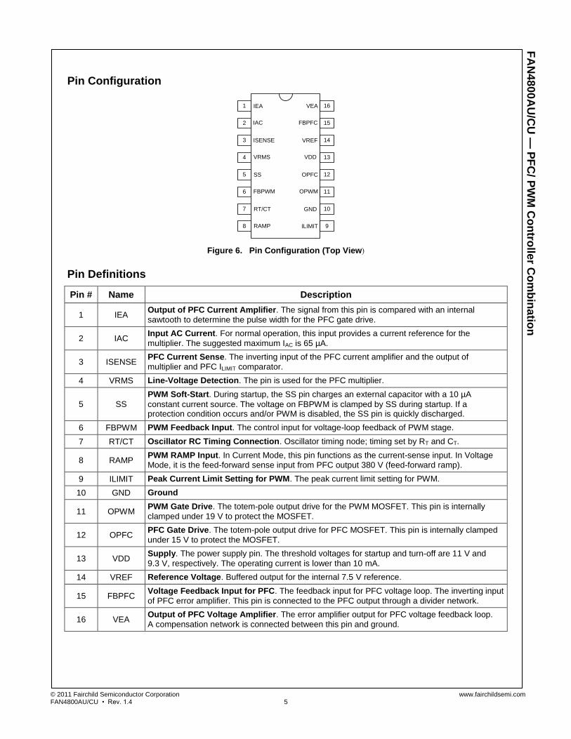
Pin Configuration
IEA
RAMP
RT/CT
FBPWM
SS
VRMS
ISENSE
IAC
ILIMIT
GND
OPWM
OPFC
VDD
VREF
FBPFC
VEA1
2
3
4
5
6
7
8
16
15
14
13
12
11
10
9
Figure 6. Pin Configuration (Top View)
Pin Definitions
Pin # Name Description
1 IEA Output of PFC Current Amplifier. The signal from this pin is compared with an internal
sawtooth to determine the pulse width for the PFC gate drive.
2 IAC Input AC Current. For normal operation, this input provides a current reference for the
multiplier. The suggested maximum IAC is 65 µA.
3 ISENSE PFC Current Sense. The inverting input of the PFC current amplifier and the output of
multiplier and PFC ILIMIT comparator.
4 VRMS Line-Voltage Detection. The pin is used for the PFC multiplier.
5 SS
PWM Soft-Start. During startup, the SS pin charges an external capacitor with a 10 µA
constant current source. The voltage on FBPWM is clamped by SS during startup. If a protection condition occurs and/or PWM is disabled, the SS pin is quickly discharged.
6 FBPWM PWM Feedback Input. The control input for voltage-loop feedback of PWM stage.
7 RT/CT Oscillator RC Timing Connection. Oscillator timing node; timing set by RT and CT.
8 RAMP PWM RAMP Input. In Current Mode, this pin functions as the current-sense input. In Voltage Mode, it is the feed-forward sense input from PFC output 380 V (feed-forward ramp).
9 ILIMIT Peak Current Limit Setting for PWM. The peak current limit setting for PWM.
10 GND Ground
11 OPWM PWM Gate Drive. The totem-pole output drive for the PWM MOSFET. This pin is internally
clamped under 19 V to protect the MOSFET.
12 OPFC PFC Gate Drive. The totem-pole output drive for PFC MOSFET. This pin is internally clamped
under 15 V to protect the MOSFET.
13 VDD Supply. The power supply pin. The threshold voltages for startup and turn-off are 11 V and
9.3 V, respectively. The operating current is lower than 10 mA.
14 VREF Reference Voltage. Buffered output for the internal 7.5 V reference.
15 FBPFC Voltage Feedback Input for PFC. The feedback input for PFC voltage loop. The inverting input
of PFC error amplifier. This pin is connected to the PFC output through a divider network.
16 VEA Output of PFC Voltage Amplifier. The error amplifier output for PFC voltage feedback loop.
A compensation network is connected between this pin and ground.
© 2011 Fairchild Semiconductor Corporation www.fairchildsemi.com FAN4800AU/CU • Rev. 1.4 6
FA
N4
80
0A
U/C
U —
PF
C/ P
WM
Co
ntro
ller C
om
bin
atio
n
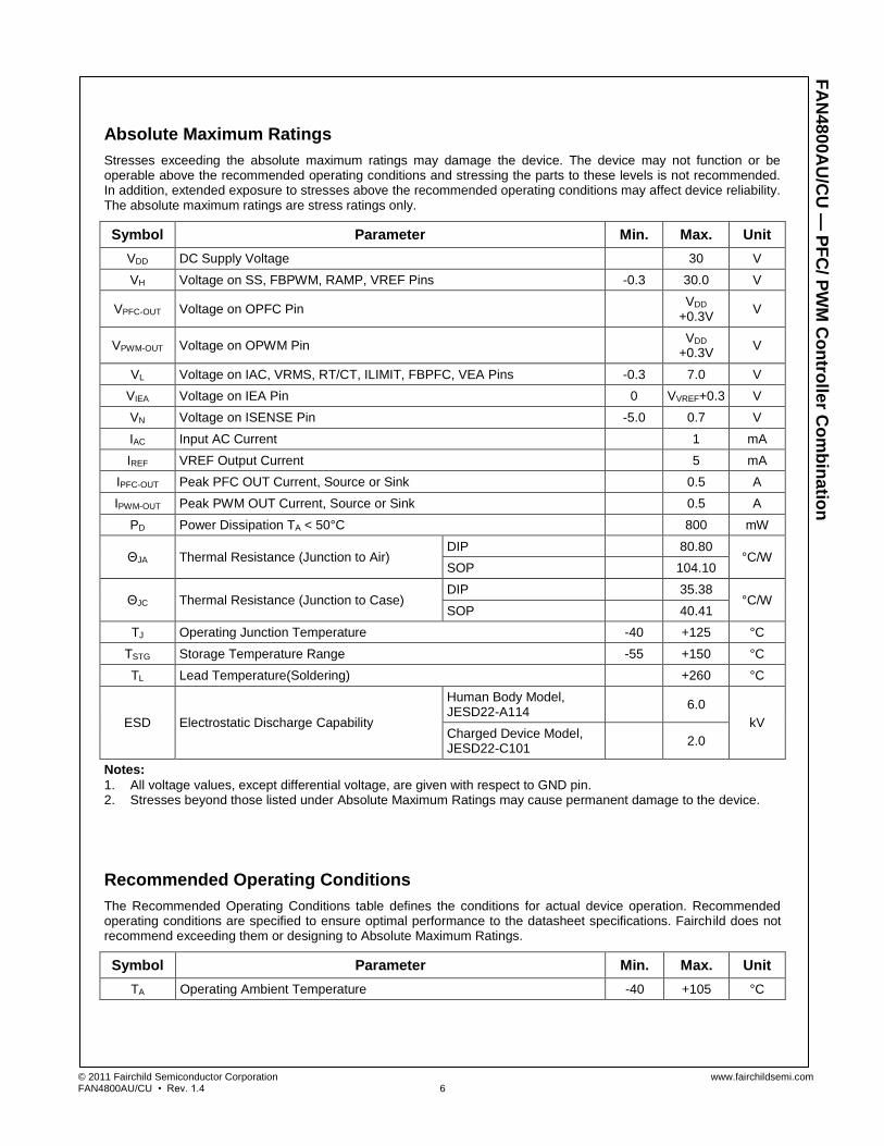
Absolute Maximum Ratings
Stresses exceeding the absolute maximum ratings may damage the device. The device may not function or be operable above the recommended operating conditions and stressing the parts to these levels is not recommended. In addition, extended exposure to stresses above the recommended operating conditions may affect device reliability. The absolute maximum ratings are stress ratings only.
Symbol Parameter Min. Max. Unit
VDD DC Supply Voltage 30 V
VH Voltage on SS, FBPWM, RAMP, VREF Pins -0.3 30.0 V
VPFC-OUT Voltage on OPFC Pin VDD
+0.3V V
VPWM-OUT Voltage on OPWM Pin VDD
+0.3V V
VL Voltage on IAC, VRMS, RT/CT, ILIMIT, FBPFC, VEA Pins -0.3 7.0 V
VIEA Voltage on IEA Pin 0 VVREF+0.3 V
VN Voltage on ISENSE Pin -5.0 0.7 V
IAC Input AC Current 1 mA
IREF VREF Output Current 5 mA
IPFC-OUT Peak PFC OUT Current, Source or Sink 0.5 A
IPWM-OUT Peak PWM OUT Current, Source or Sink 0.5 A
PD Power Dissipation TA < 50°C 800 mW
ΘJA Thermal Resistance (Junction to Air) DIP 80.80
°C/W SOP 104.10
ΘJC Thermal Resistance (Junction to Case) DIP 35.38
°C/W SOP 40.41
TJ Operating Junction Temperature -40 +125 °C
TSTG Storage Temperature Range -55 +150 °C
TL Lead Temperature(Soldering) +260 °C
ESD Electrostatic Discharge Capability
Human Body Model, JESD22-A114
6.0
kV Charged Device Model, JESD22-C101
2.0
Notes:
1. All voltage values, except differential voltage, are given with respect to GND pin. 2. Stresses beyond those listed under Absolute Maximum Ratings may cause permanent damage to the device.
Recommended Operating Conditions
The Recommended Operating Conditions table defines the conditions for actual device operation. Recommended operating conditions are specified to ensure optimal performance to the datasheet specifications. Fairchild does not recommend exceeding them or designing to Absolute Maximum Ratings.
Symbol Parameter Min. Max. Unit
TA Operating Ambient Temperature -40 +105 °C
© 2011 Fairchild Semiconductor Corporation www.fairchildsemi.com FAN4800AU/CU • Rev. 1.4 7
FA
N4
80
0A
U/C
U —
PF
C/ P
WM
Co
ntro
ller C
om
bin
atio
n
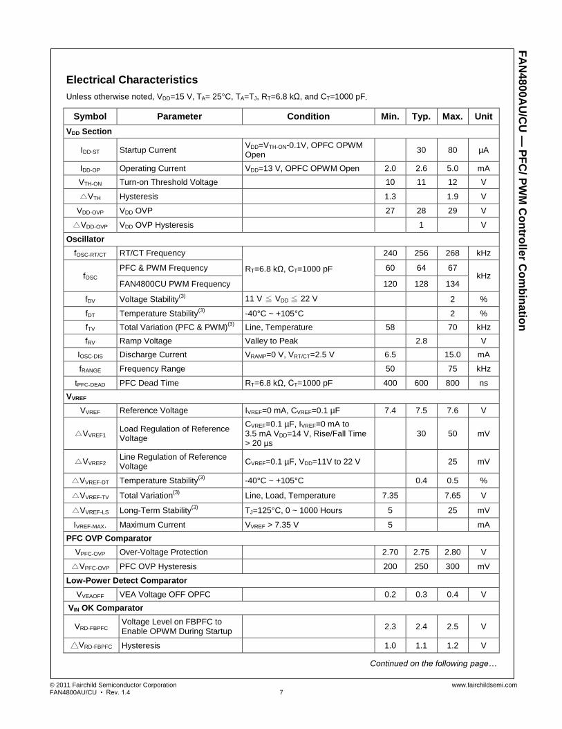
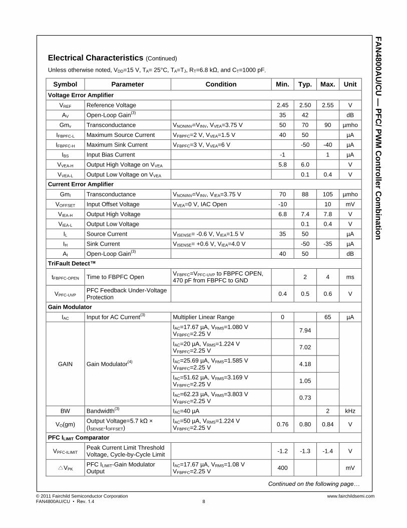
Electrical Characteristics
Unless otherwise noted, VDD=15 V, TA= 25°C, TA=TJ, RT=6.8 kΩ, and CT=1000 pF.
Symbol Parameter Condition Min. Typ. Max. Unit
VDD Section
IDD-ST Startup Current VDD=VTH-ON-0.1V, OPFC OPWM Open
30 80 µA
IDD-OP Operating Current VDD=13 V, OPFC OPWM Open 2.0 2.6 5.0 mA
VTH-ON Turn-on Threshold Voltage 10 11 12 V
VTH Hysteresis 1.3 1.9 V
VDD-OVP VDD OVP 27 28 29 V
VDD-OVP VDD OVP Hysteresis 1 V
Oscillator
fOSC-RT/CT RT/CT Frequency
RT=6.8 kΩ, CT=1000 pF
240 256 268 kHz
fOSC PFC & PWM Frequency 60 64 67
kHz FAN4800CU PWM Frequency 120 128 134
fDV Voltage Stability(3)
11 V ≦ VDD ≦ 22 V 2 %
fDT Temperature Stability(3)
-40°C ~ +105°C 2 %
fTV Total Variation (PFC & PWM)(3)
Line, Temperature 58 70 kHz
fRV Ramp Voltage Valley to Peak 2.8 V
IOSC-DIS Discharge Current VRAMP=0 V, VRT/CT=2.5 V 6.5 15.0 mA
fRANGE Frequency Range 50 75 kHz
tPFC-DEAD PFC Dead Time RT=6.8 kΩ, CT=1000 pF 400 600 800 ns
VVREF
VVREF Reference Voltage IVREF=0 mA, CVREF=0.1 µF 7.4 7.5 7.6 V
VVREF1 Load Regulation of Reference Voltage
CVREF=0.1 µF, IVREF=0 mA to 3.5 mA VDD=14 V, Rise/Fall Time > 20 µs
30 50 mV
VVREF2 Line Regulation of Reference Voltage
CVREF=0.1 µF, VDD=11V to 22 V 25 mV
VVREF-DT Temperature Stability(3)
-40°C ~ +105°C 0.4 0.5 %
VVREF-TV Total Variation(3)
Line, Load, Temperature 7.35 7.65 V
VVREF-LS Long-Term Stability(3)
TJ=125°C, 0 ~ 1000 Hours 5 25 mV
IVREF-MAX. Maximum Current VVREF > 7.35 V 5 mA
PFC OVP Comparator
VPFC-OVP Over-Voltage Protection 2.70 2.75 2.80 V
VPFC-OVP PFC OVP Hysteresis 200 250 300 mV
Low-Power Detect Comparator
VVEAOFF VEA Voltage OFF OPFC 0.2 0.3 0.4 V
VIN OK Comparator
VRD-FBPFC Voltage Level on FBPFC to Enable OPWM During Startup
2.3 2.4 2.5 V
VRD-FBPFC Hysteresis 1.0 1.1 1.2 V
Continued on the following page…
© 2011 Fairchild Semiconductor Corporation www.fairchildsemi.com FAN4800AU/CU • Rev. 1.4 8
FA
N4
80
0A
U/C
U —
PF
C/ P
WM
Co
ntro
ller C
om
bin
atio
n
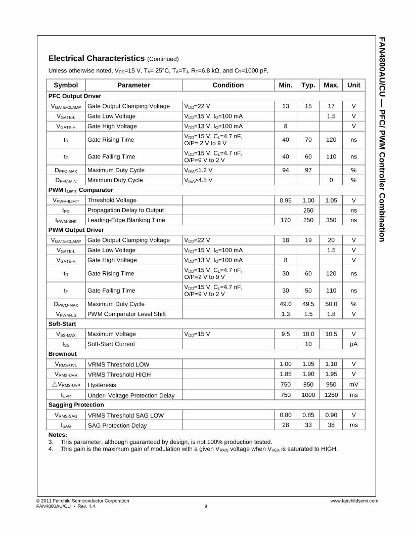
Electrical Characteristics (Continued)
Unless otherwise noted, VDD=15 V, TA= 25°C, TA=TJ, RT=6.8 kΩ, and CT=1000 pF.
Symbol Parameter Condition Min. Typ. Max. Unit
Voltage Error Amplifier
VREF Reference Voltage 2.45 2.50 2.55 V
AV Open-Loop Gain(3)
35 42 dB
Gmv Transconductance VNONINV=VINV, VVEA=3.75 V 50 70 90 µmho
IFBPFC-L Maximum Source Current VFBPFC=2 V, VVEA=1.5 V 40 50 µA
IFBPFC-H Maximum Sink Current VFBPFC=3 V, VVEA=6 V -50 -40 µA
IBS Input Bias Current -1 1 µA
VVEA-H Output High Voltage on VVEA 5.8 6.0 V
VVEA-L Output Low Voltage on VVEA 0.1 0.4 V
Current Error Amplifier
GmI Transconductance VNONINV=VINV, VIEA=3.75 V 70 88 105 µmho
VOFFSET Input Offset Voltage VVEA=0 V, IAC Open -10 10 mV
VIEA-H Output High Voltage 6.8 7.4 7.8 V
VIEA-L Output Low Voltage 0.1 0.4 V
IL Source Current VISENSE= -0.6 V, VIEA=1.5 V 35 50 µA
IH Sink Current VISENSE= +0.6 V, VIEA=4.0 V -50 -35 µA
AI Open-Loop Gain(3)
40 50 dB
TriFault Detect™
tFBPFC-OPEN Time to FBPFC Open VFBPFC=VPFC-UVP to FBPFC OPEN, 470 pF from FBPFC to GND
2 4 ms
VPFC-UVP PFC Feedback Under-Voltage Protection
0.4 0.5 0.6 V
Gain Modulator
IAC Input for AC Current(3)
Multiplier Linear Range 0 65 µA
GAIN Gain Modulator(4)
IAC=17.67 µA, VRMS=1.080 V VFBPFC=2.25 V
7.94
IAC=20 µA, VRMS=1.224 V VFBPFC=2.25 V
7.02
IAC=25.69 µA, VRMS=1.585 V VFBPFC=2.25 V
4.18
IAC=51.62 µA, VRMS=3.169 V VFBPFC=2.25 V
1.05
IAC=62.23 µA, VRMS=3.803 V VFBPFC=2.25 V
0.73
BW Bandwidth(3)
IAC=40 µA 2 kHz
VO(gm) Output Voltage=5.7 kΩ × (ISENSE-IOFFSET)
IAC=50 µA, VRMS=1.224 V VFBPFC=2.25 V
0.76 0.80 0.84 V
PFC ILIMIT Comparator
VPFC-ILIMIT Peak Current Limit Threshold Voltage, Cycle-by-Cycle Limit
-1.2 -1.3 -1.4 V
VPK PFC ILIMIT-Gain Modulator Output
IAC=17.67 µA, VRMS=1.08 V VFBPFC=2.25 V
400 mV
Continued on the following page…
© 2011 Fairchild Semiconductor Corporation www.fairchildsemi.com FAN4800AU/CU • Rev. 1.4 9
FA
N4
80
0A
U/C
U —
PF
C/ P
WM
Co
ntro
ller C
om
bin
atio
n
Electrical Characteristics (Continued)
Unless otherwise noted, VDD=15 V, TA= 25°C, TA=TJ, RT=6.8 kΩ, and CT=1000 pF.
Symbol Parameter Condition Min. Typ. Max. Unit
PFC Output Driver
VGATE-CLAMP Gate Output Clamping Voltage VDD=22 V 13 15 17 V
VGATE-L Gate Low Voltage VDD=15 V, IO=100 mA 1.5 V
VGATE-H Gate High Voltage VDD=13 V, IO=100 mA 8 V
tR Gate Rising Time VDD=15 V, CL=4.7 nF, O/P= 2 V to 9 V
40 70 120 ns
tF Gate Falling Time VDD=15 V, CL=4.7 nF, O/P=9 V to 2 V
40 60 110 ns
DPFC-MAX Maximum Duty Cycle VIEA<1.2 V 94 97 %
DPFC-MIN Minimum Duty Cycle VIEA>4.5 V 0 %
PWM ILIMIT Comparator
VPWM-ILIMIT Threshold Voltage 0.95 1.00 1.05 V
tPD Propagation Delay to Output 250 ns
tPWM-BNK Leading-Edge Blanking Time 170 250 350 ns
PWM Output Driver
VGATE-CLAMP Gate Output Clamping Voltage VDD=22 V 18 19 20 V
VGATE-L Gate Low Voltage VDD=15 V, IO=100 mA 1.5 V
VGATE-H Gate High Voltage VDD=13 V, IO=100 mA 8 V
tR Gate Rising Time VDD=15 V, CL=4.7 nF, O/P=2 V to 9 V
30 60 120 ns
tF Gate Falling Time VDD=15 V, CL=4.7 nF, O/P=9 V to 2 V
30 50 110 ns
DPWM-MAX Maximum Duty Cycle 49.0 49.5 50.0 %
VPWM-LS PWM Comparator Level Shift 1.3 1.5 1.8 V
Soft-Start
VSS-MAX Maximum Voltage VDD=15 V 9.5 10.0 10.5 V
ISS Soft-Start Current 10 µA
Brownout
VRMS-UVL VRMS Threshold LOW 1.00 1.05 1.10 V
VRMS-UVH VRMS Threshold HIGH 1.85 1.90 1.95 V
VRMS-UVP Hysteresis 750 850 950 mV
tUVP Under- Voltage Protection Delay 750 1000 1250 ms
Sagging Protection
VRMS-SAG VRMS Threshold SAG LOW 0.80 0.85 0.90 V
tSAG SAG Protection Delay 28 33 38 ms
Notes:
3. This parameter, although guaranteed by design, is not 100% production tested. 4. This gain is the maximum gain of modulation with a given VRMS voltage when VVEA is saturated to HIGH.
© 2011 Fairchild Semiconductor Corporation www.fairchildsemi.com FAN4800AU/CU • Rev. 1.4 10
FA
N4
80
0A
U/C
U —
PF
C/ P
WM
Co
ntro
ller C
om
bin
atio
n
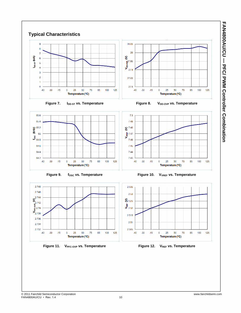
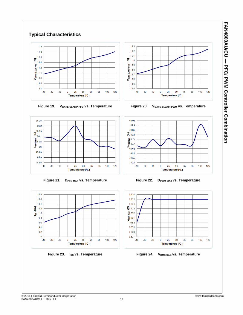
Typical Characteristics
Figure 7. IDD-ST vs. Temperature Figure 8. VDD-OVP vs. Temperature
Figure 9. fOSC vs. Temperature Figure 10. VVREF vs. Temperature
Figure 11. VPFC-OVP vs. Temperature Figure 12. VREF vs. Temperature
© 2011 Fairchild Semiconductor Corporation www.fairchildsemi.com FAN4800AU/CU • Rev. 1.4 11
FA
N4
80
0A
U/C
U —
PF
C/ P
WM
Co
ntro
ller C
om
bin
atio
n
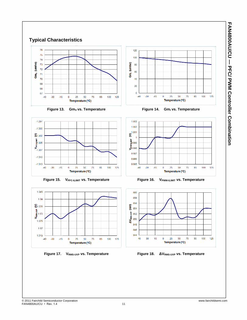
Typical Characteristics
Figure 13. GmV vs. Temperature Figure 14. GmI vs. Temperature
Figure 15. VPFC-ILIMIT vs. Temperature Figure 16. VPWM-ILIMIT vs. Temperature
Figure 17. VRMS-UVP vs. Temperature Figure 18. ΔVRMS-UVP vs. Temperature
© 2011 Fairchild Semiconductor Corporation www.fairchildsemi.com FAN4800AU/CU • Rev. 1.4 12
FA
N4
80
0A
U/C
U —
PF
C/ P
WM
Co
ntro
ller C
om
bin
atio
n
Typical Characteristics
Figure 19. VGATE-CLAMP-PFC vs. Temperature Figure 20. VGATE-CLAMP-PWM vs. Temperature
Figure 21. DPFC-MAX vs. Temperature Figure 22. DPWM-MAX vs. Temperature
Figure 23. ISS vs. Temperature Figure 24. VRMS-SAG vs. Temperature
FA
N4
80
0A
U/C
U —
PF
C/ P
WM
Co
ntro
ller C
om
bin
atio
n
© 2011 Fairchild Semiconductor Corporation www.fairchildsemi.com FAN4800AU/CU • Rev. 1.4
Functional Description
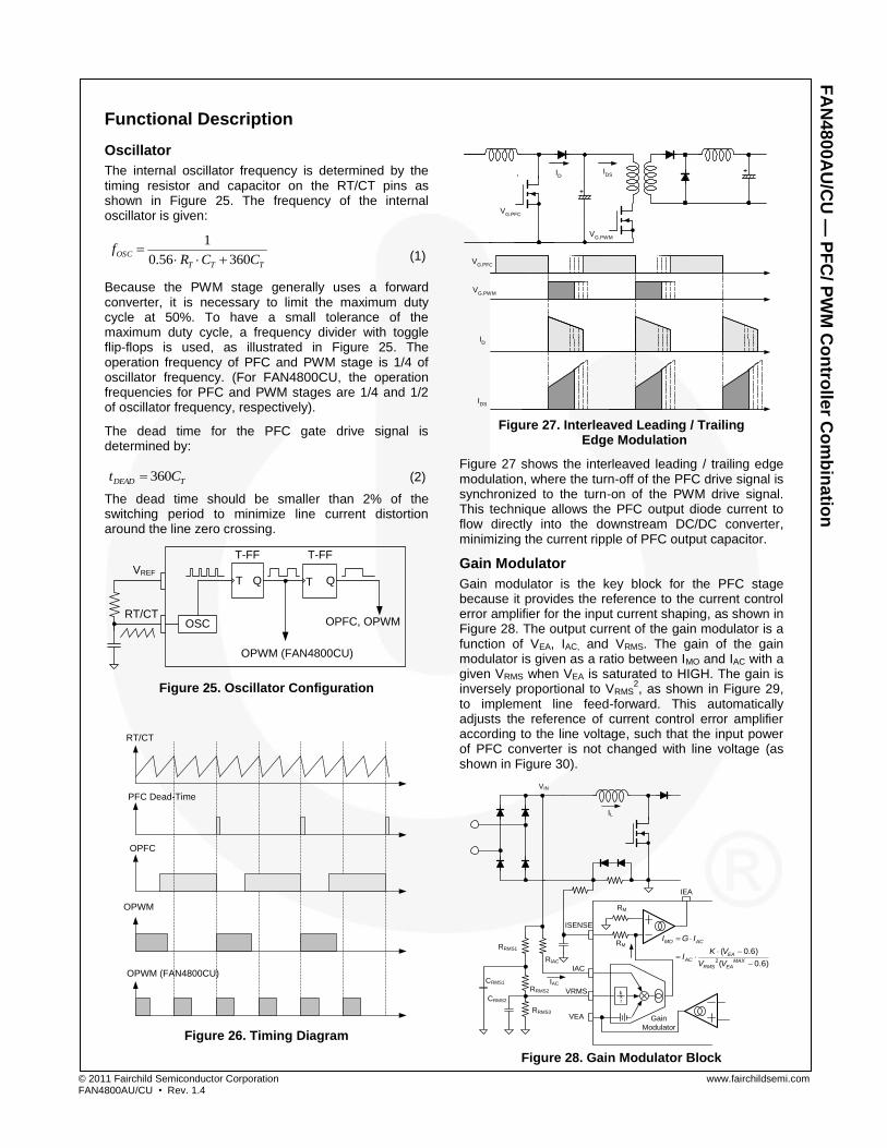
Oscillator
The internal oscillator frequency is determined by the timing resistor and capacitor on the RT/CT pins as shown in Figure 25. The frequency of the internal oscillator is given:
TTT
OSCCCR
f36056.0
1
(1)
Because the PWM stage generally uses a forward converter, it is necessary to limit the maximum duty cycle at 50%. To have a small tolerance of the maximum duty cycle, a frequency divider with toggle flip-flops is used, as illustrated in Figure 25. The operation frequency of PFC and PWM stage is 1/4 of oscillator frequency. (For FAN4800CU, the operation frequencies for PFC and PWM stages are 1/4 and 1/2 of oscillator frequency, respectively).
The dead time for the PFC gate drive signal is determined by:
TDEAD Ct 360 (2)
The dead time should be smaller than 2% of the switching period to minimize line current distortion around the line zero crossing.
RT/CT
VREF
OSC
T Q
T-FF
T Q
OPWM (FAN4800CU)
OPFC, OPWM
T-FF
Figure 25. Oscillator Configuration
RT/CT
OPFC
OPWM
OPWM (FAN4800CU)
PFC Dead-Time
Figure 26. Timing Diagram
ID
IDS
VG.PFC
VG.PWM
VG.PFC
VG.PWM
IDS
ID
Figure 27. Interleaved Leading / Trailing
Edge Modulation
Figure 27 shows the interleaved leading / trailing edge modulation, where the turn-off of the PFC drive signal is synchronized to the turn-on of the PWM drive signal. This technique allows the PFC output diode current to flow directly into the downstream DC/DC converter, minimizing the current ripple of PFC output capacitor.
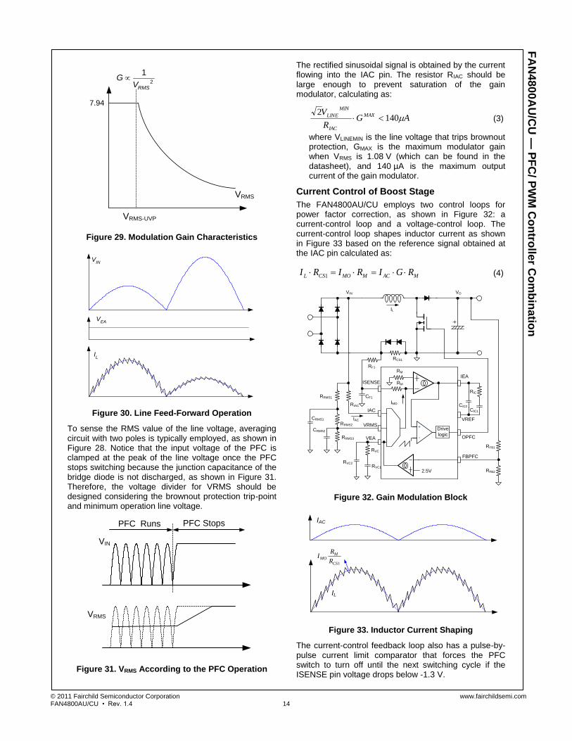
Gain Modulator
Gain modulator is the key block for the PFC stage because it provides the reference to the current control error amplifier for the input current shaping, as shown in Figure 28. The output current of the gain modulator is a function of VEA, IAC, and VRMS. The gain of the gain modulator is given as a ratio between IMO and IAC with a given VRMS when VEA is saturated to HIGH. The gain is inversely proportional to VRMS
2, as shown in Figure 29,
to implement line feed-forward. This automatically adjusts the reference of current control error amplifier according to the line voltage, such that the input power of PFC converter is not changed with line voltage (as shown in Figure 30).
ISENSE
IAC
VRMS
VEA
2
( 0.6)
( 0.6)
MO AC
EAAC MAX
RMS EA
I G I
K VI
V V
IEA
RM
RM
Gain
Modulator
RRMS1
RRMS2
RRMS3
CRMS1
CRMS2
RIAC
IAC
VIN
IL
x2
k
Figure 28. Gain Modulator Block
© 2011 Fairchild Semiconductor Corporation www.fairchildsemi.com FAN4800AU/CU • Rev. 1.4 14
FA
N4
80
0A
U/C
U —
PF
C/ P
WM
Co
ntro
ller C
om
bin
atio
n
VRMS
VRMS-UVP
2
1
RMS
GV
7.94
Figure 29. Modulation Gain Characteristics
VIN
IL
VEA
Figure 30. Line Feed-Forward Operation
To sense the RMS value of the line voltage, averaging circuit with two poles is typically employed, as shown in Figure 28. Notice that the input voltage of the PFC is clamped at the peak of the line voltage once the PFC stops switching because the junction capacitance of the bridge diode is not discharged, as shown in Figure 31. Therefore, the voltage divider for VRMS should be designed considering the brownout protection trip-point and minimum operation line voltage.
PFC Runs PFC Stops
VIN
VRMS
Figure 31. VRMS According to the PFC Operation
The rectified sinusoidal signal is obtained by the current flowing into the IAC pin. The resistor RIAC should be large enough to prevent saturation of the gain modulator, calculating as:
AGR
V MAX
IAC
MIN
LINE 1402
(3)
where VLINEMIN is the line voltage that trips brownout protection, GMAX is the maximum modulator gain when VRMS is 1.08 V (which can be found in the datasheet), and 140 µA is the maximum output current of the gain modulator.
Current Control of Boost Stage
The FAN4800AU/CU employs two control loops for power factor correction, as shown in Figure 32: a current-control loop and a voltage-control loop. The current-control loop shapes inductor current as shown in Figure 33 based on the reference signal obtained at the IAC pin calculated as:
MACMMOCSL RGIRIRI 1 (4)
ISENSE
IAC
VRMS
VEA
IEARM
RM
RRMS1
RRMS2
RRMS3
CRMS1
CRMS2
RIAC
IAC
VIN
IL
RCS1
RF1
CF1
IMO
RIC
CIC1
CIC2
+
-
Drive
logicOPFC
2.5V
RVC
RVC1
RVC2
FBPFC
RFB1
RFB2
VO
VREF
Figure 32. Gain Modulation Block
IAC
IL
1
MMO
CS
RI
R
Figure 33. Inductor Current Shaping
The current-control feedback loop also has a pulse-by-pulse current limit comparator that forces the PFC switch to turn off until the next switching cycle if the ISENSE pin voltage drops below -1.3 V.
© 2011 Fairchild Semiconductor Corporation www.fairchildsemi.com FAN4800AU/CU • Rev. 1.4 15
FA
N4
80
0A
U/C
U —
PF
C/ P
WM
Co
ntro
ller C
om
bin
atio
n
Voltage Control of Boost Stage
The voltage-control loop regulates PFC output voltage using an internal error amplifier such that the FB voltage is the same as the internal reference of 2.5 V.
Brownout Protection
The built-in internal brownout protection comparator monitors the voltage of the VRMS pin. Once VRMS pin voltage is lower than 1.05 V, the PFC stage is shut down to protect the system from over current. FAN4800AU/CU starts up the boost stage once VRMS voltage increases above 1.9 V.
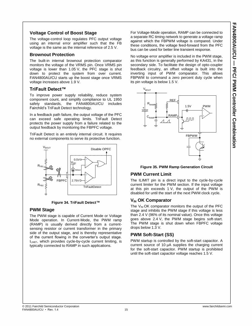
TriFault Detect™
To improve power supply reliability, reduce system component count, and simplify compliance to UL 1950 safety standards, the FAN4800AU/CU includes Fairchild’s TriFault Detect technology.
In a feedback path failure, the output voltage of the PFC can exceed safe operating limits. TriFault Detect protects the power supply from a failure related to the output feedback by monitoring the FBPFC voltage.
TriFault Detect is an entirely internal circuit. It requires no external components to serve its protective function.
VBOUT
RFB1
RFB2
FBPFC
Disable OPFC
TriFaultDetect
+
-
+
-
0.5V
2.75V
VDD
300nA
Figure 34. TriFault Detect™
PWM Stage
The PWM stage is capable of Current Mode or Voltage Mode operation. In Current-Mode, the PWM ramp (RAMP) is usually derived directly from a current-sensing resistor or current transformer in the primary side of the output stage, and is thereby representative of the current flowing in the converter’s output stage. ILIMIT, which provides cycle-by-cycle current limiting, is typically connected to RAMP in such applications.
For Voltage-Mode operation, RAMP can be connected to a separate RC timing network to generate a voltage ramp against which the FBPWM voltage is compared. Under these conditions, the voltage feed-forward from the PFC bus can be used for better line transient response.
No voltage error amplifier is included in the PWM stage, as this function is generally performed by KA431, in the secondary side. To facilitate the design of opto-coupler feedback circuitry, an offset voltage is built into the inverting input of PWM comparator. This allows FBPWM to command a zero percent duty cycle when its pin voltage is below 1.5 V.
VBOUT
RAMP
RRAMP
CRAMP
REF
+
-
PWM
FBPWM
1.5V
Figure 35. PWM Ramp Generation Circuit
PWM Current Limit
The ILIMIT pin is a direct input to the cycle-by-cycle current limiter for the PWM section. If the input voltage at this pin exceeds 1 V, the output of the PWM is disabled for until the start of the next PWM clock cycle.
VIN OK Comparator
The VIN OK comparator monitors the output of the PFC stage and inhibits the PWM stage if this voltage is less than 2.4 V (96% of its nominal value). Once this voltage goes above 2.4 V, the PWM stage begins soft-start. The PWM stage is shut down when FBPFC voltage drops below 1.3 V.
PWM Soft-Start (SS)
PWM startup is controlled by the soft-start capacitor. A current source of 10 µA supplies the charging current
for the soft-start capacitor. PWM startup is prohibited until the soft-start capacitor voltage reaches 1.5 V.
© 2011 Fairchild Semiconductor Corporation www.fairchildsemi.com FAN4800AU/CU • Rev. 1.4 16
FA
N4
80
0A
U/C
U —
PF
C/ P
WM
Co
ntro
ller C
om
bin
atio
n
AC Line Drops Out
FAN4800AU/CU is designed such that the operation of PFC part is not perturbed by AC line dropout. Once line voltage disappears, the error amplifier can be saturated, resulting in abnormal current waveforms when the line voltage is recovered if proper preventive measures are not employed.
With a limited gain modulator operation, FAN4800AU /CU guarantees stable PFC operation even when AC line is recovered from dropout, as shown in Figure 36.
VIN
VEA
VRMS
PFC ILIMIT
Vo(gm)
VEA Saturation
IL
Figure 36. AC Cycle Drop
Line Sag Protection
When the line sags below its normal operational range, the PFC part keeps operating until the brownout protection is triggered, which has 1 s debounce time. Due to the low line voltage, the gain modulator for current loop is saturated and input current of PFC is limited, resulting in a drop of the PFC output voltage at heavy-load condition. Since the PWM part has a VIN OK comparator that shuts down PWM operation when the FBPFC voltage drops below 1.3 V, the downstream DC-DC converter can stop operation while the PFC output voltage drops during line sag. Once the downstream converter stops operation, even the limited PFC input current can charge up the PFC output since the PFC part has no load current. Because this can cause repeated startup and shutdown of downstream converter during line sag, FAN4800AU/CU has line sag protection.
There are two conditions that trigger line sag protection, as shown in Figure 37 and Figure 38. The first condition is when VRMS is lower than VRMS-SAG (0.85 V) for longer than tSAG (33 ms), as shown in Figure 37. The second condition is when VRMS is lower than VRMS-SAG (0.85 V) and VFBPFC is lower than VIN-OFF (1.3 V), as shown in Figure 38. Once line sag protection is triggered, the PWM and the PFC stop operation until VRMS increases above 1.9 V.
VFBPFC
VIN
VRMS
0.85V
33ms
Figure 37. The First Condition of Sag Protection
VFBPFC
VIN
VRMS
0.85V
25ms
1.3V
Figure 38. The Second condition of Sag Protection
5.33 MAX
0.38 MIN
4.952.92
3.812.92
1.781.14
0.560.36 2.54
FRONT VIEW
C
19.6918.67
7.116.10
(0.40) TOP VIEW
A
B
0.280.20
10.92
8.257.62
SIDE VIEW
NOTES:A. CONFORMS TO JEDEC MS-001, VARIATION BB B. ALL DIMENSIONS ARE IN MILLIMETERSC. DIMENSIONS ARE EXCLUSIVE OF BURRS, MOLD FLASH, AND TIE BAR PROTRUSIONSD. DIMENSIONS AND TOLERANCES PER ASME Y14.5M-2009E. DRAWING FILENAME: MKT-N16Erev3
1 8
916
0.25 M C
PIN #1
FRONT VIEW
TOP VIEW
8°
0°
SEE DETAIL A
SEATING PLANE
C
GAGE PLANE
x 45°
DETAIL A
SCALE: 2:1
B
A
6.00
8.89
4.00
3.80
10.00
9.80
(0.30)
1.27
0.25
0.05
1.75 MAX
0.25
0.19
0.36
0.50
0.25
R0.10
R0.10
0.90
0.50 (1.04)
0.25 C B A
0.10 C
NOTES:
A) THIS PACKAGE CONFORMS TO JEDEC
MS-012, VARIATION AC, ISSUE C.
B) ALL DIMENSIONS ARE IN MILLIMETERS.
C) DIMENSIONS ARE EXCLUSIVE OF BURRS,
MOLD FLASH AND TIE BAR PROTRUSIONS
D) CONFORMS TO ASME Y14.5M-2009
E) LANDPATTERN STANDARD:
SOIC127P600X175-16AM
F) DRAWING FILE NAME: M16AREV13.
LAND PATTERN RECOMMENDATION
1
16
8
9
0.51
0.31
1.50
1.25
3.85
7.35
1.27
0.65
1.75
8.89
www.onsemi.com1
ON Semiconductor and are trademarks of Semiconductor Components Industries, LLC dba ON Semiconductor or its subsidiaries in the United States and/or other countries.ON Semiconductor owns the rights to a number of patents, trademarks, copyrights, trade secrets, and other intellectual property. A listing of ON Semiconductor’s product/patentcoverage may be accessed at www.onsemi.com/site/pdf/Patent−Marking.pdf. ON Semiconductor reserves the right to make changes without further notice to any products herein.ON Semiconductor makes no warranty, representation or guarantee regarding the suitability of its products for any particular purpose, nor does ON Semiconductor assume any liabilityarising out of the application or use of any product or circuit, and specifically disclaims any and all liability, including without limitation special, consequential or incidental damages.Buyer is responsible for its products and applications using ON Semiconductor products, including compliance with all laws, regulations and safety requirements or standards,regardless of any support or applications information provided by ON Semiconductor. “Typical” parameters which may be provided in ON Semiconductor data sheets and/orspecifications can and do vary in different applications and actual performance may vary over time. All operating parameters, including “Typicals” must be validated for each customerapplication by customer’s technical experts. ON Semiconductor does not convey any license under its patent rights nor the rights of others. ON Semiconductor products are notdesigned, intended, or authorized for use as a critical component in life support systems or any FDA Class 3 medical devices or medical devices with a same or similar classificationin a foreign jurisdiction or any devices intended for implantation in the human body. Should Buyer purchase or use ON Semiconductor products for any such unintended or unauthorizedapplication, Buyer shall indemnify and hold ON Semiconductor and its officers, employees, subsidiaries, affiliates, and distributors harmless against all claims, costs, damages, andexpenses, and reasonable attorney fees arising out of, directly or indirectly, any claim of personal injury or death associated with such unintended or unauthorized use, even if suchclaim alleges that ON Semiconductor was negligent regarding the design or manufacture of the part. ON Semiconductor is an Equal Opportunity/Affirmative Action Employer. Thisliterature is subject to all applicable copyright laws and is not for resale in any manner.
PUBLICATION ORDERING INFORMATIONN. American Technical Support: 800−282−9855 Toll FreeUSA/Canada
Europe, Middle East and Africa Technical Support:Phone: 421 33 790 2910
Japan Customer Focus CenterPhone: 81−3−5817−1050
www.onsemi.com
LITERATURE FULFILLMENT:Literature Distribution Center for ON Semiconductor19521 E. 32nd Pkwy, Aurora, Colorado 80011 USAPhone: 303−675−2175 or 800−344−3860 Toll Free USA/CanadaFax: 303−675−2176 or 800−344−3867 Toll Free USA/CanadaEmail: [email protected]
ON Semiconductor Website: www.onsemi.com
Order Literature: http://www.onsemi.com/orderlit
For additional information, please contact your localSales Representative
© Semiconductor Components Industries, LLC
Related Documents