WARSAW UNIVERSITY OF TECHNOLOGY Faculty of Electronics and Information Technology Ph.D. THESIS Waldemar Koprek, M.Sc. A Flexible Electronic Tool for Development of VXI Message-based Devices Supervisor Professor Konrad Hejn, Ph.D., D.Sc. Warsaw, 2008

Welcome message from author
This document is posted to help you gain knowledge. Please leave a comment to let me know what you think about it! Share it to your friends and learn new things together.
Transcript
WARSAW UNIVERSITYOF TECHNOLOGY
Faculty of Electronicsand Information Technology
Ph.D. THESIS
Waldemar Koprek, M.Sc.
A Flexible Electronic Tool for Developmentof VXI Message-based Devices
SupervisorProfessor Konrad Hejn, Ph.D., D.Sc.
Warsaw, 2008

2

Acknowledgments
First, I would like to express my deep gratitude to my supervisor Prof. Konrad Hejn for the
inspiration and guidance that helped me tremendously in preparation of this dissertation.
Special thanks are addressed to Dr. Jerzy Jedrachowicz, Dr. Antoni Lesniewski and Dr.
Sławomir Sobczak from Research Group on Automatic Test Systems in Institute of Electronic
Systems for their valuable suggestions, technical support and work evaluation.
I would like to thank Dr. Stefan Simrock from DESY for his continuous support and
encouragement.
Finally, I want to thank my wife Monika for her inexhaustible patience and support, especially
in the last period of my work.
I acknowledge the support of Polish Ministry of Science in year 2007/2008 within the scope
of the research project N505 005 32/0598.
3
Abstract
The VXI/SCPI technology has been used for more than fifteen years. Due to the high priceof modern measurement and control systems, it was necessary to standardize their development.Only then could the integration of hardware and software be done in a reasonable time and withlimited costs. The currently available standards are complex and hard to understand, whichcauses problems with their implementation. Hence, the small manufacturers and laboratorieshave been eliminated from this market. An integration of commercially available VXI devicesinto a system is indeed costly but requires little effort, particularly in the case of message–baseddevices programmable by SCPI. The situation becomes much more difficult when the developerof a system must integrate a piece of electronics specific to his needs. Transformation intoa message-based device is difficult due to the complexity of the IEEE 488.2 and VXI standards,and SCPI specification.
Having in mind all these problems, the thesis was stated as follows: it is possible in a smalllaboratory environment to design an effective tool that is flexible enough to integrate somespecific electronics into a VXI/SCPI system as a message-based device.
The goal of this thesis was to build a universal tool that supports development of VXImessage-based devices programmable by SCPI messages and compatible with the VXI stan-dard. Taking advantage of original features of the tool, a new methodology of VXI message-based devices design was proposed. It shows how to speed up and simplify the development ofnew devices.
Within the scope of this work, an electronic tool was designed and built. The tool consistsof a hardware board (VXI-IC) and associated software (VXI-SDK). VXI-IC is an electroniccard with an area less than one third that of the C size VXI module and is equipped with P1and P2 connectors. The user electronics is located on a separate board connected mechanicallyand electrically through a standard 96-pin, 3-row device connector; VXI-IC and user boardform together a C size VXI module. The VXI-IC card was built around a modern FPGAchip, Virtex II Pro from Xilinx, which contains an embedded processor. This FPGA chipallowed implementation of a complete VXI interface compatible with the IEEE 488.2 standard.The VXI-IC contains firmware that parses and formats SCPI messages, executes a device driver,and communicates with the user electronics.
VXI-SDK is a software development kit associated with VXI-IC. It is used to configureVXI-IC, and to define new SCPI commands specific to the adapted electronics. VXI-SDK alsocontains an editor for writing ANSI-C code for the device driver executed in VXI-IC.
The tool was tested with a resonant cavity controller for the FLASH accelerator at DESYin Hamburg. The existing functionality of the controller was extended by a SCPI driver anda VXI synchronization mechanism.
The tool can be an inspiration for research on message-based devices in the new and excitingLXI technology.
4

Streszczenie
Elastyczne narzedzie elektroniczne do rozwojukomunikatowych przyrzadów VXI
Technologia VXI/SCPI została po raz pierwszy zastosowana do konstrukcji inteligentnychprzyrzadów pomiarowych około pietnastu lat temu. Ze wzgledu na wysoka cene współcze-snych systemów pomiarowo–sterujacych (SPOM), konieczne było podporzadkowanie ich pro-jektowania ogólnie przyjetym standardom. Tylko wtedy bowiem integracja sprzetu i opro-gramowania okazała sie procesem o akceptowalnym horyzoncie czasowym, a perspektywauzytecznosci systemu mogła byc liczona przynajmniej w dziesiatkach lat. Obecnie problempolega miedzy innymi na tym, ze dostepne normy aparaturowe sa w swej znakomitej wie-kszosci trudne do zrozumienia i implementacji. Dlatego mniejsi producenci (nie mówiaco laboratoriach badawczych) zostali całkowicie wyeliminowani z tego atrakcyjnego rynku.Dopiero pojawienie sie układów FPGA z wbudowanym procesorem stworzyło potencjalnaszanse stworzenia narzedzia, które uwolniłoby projektanta SPOM od wielu –– wprawdziedostepnych szczegółów –– ale jednoczesnie głeboko ukrytych w tekstach obowiazujacych gonorm. Problem ten jest szczególnie wazny w przypadku konstrukcji przyrzadów komunika-towych VXI, gdzie wymagana jest dogłebna znajomosc standardów VXI i IEEE 488.2, a takzespecyfikacji SCPI.
W zwiazku z powyzszym, w pracy została postawiona nastepujaca teza. Mozliwe jeststworzenie elastycznego narzedzia, które pozwala w warunkach laboratoryjnych na tra-nsformacje specyficznej elektroniki uzytkownika w komunikatowy przyrzad standarduVXI.
Koncepcja tej pracy zakładała stworzenie uniwersalnego narzedzia wspomagajacego pro-jektowanie przyrzadów programowalnych z poziomu zbioru komend SCPI i kompatybilnychsprzetowo ze standardem interfejsu VXI. Dzieki takiemu narzedziu, projektowany przyrzad jestwidziany w srodowisku sprzetowym VXI i programowym zbioru komend SCPI jako przyrzadtypu komunikatowego.
W pracy zaproponowano metodologie budowy takich przyrzadów w oparciu o zaproje-ktowane narzedzie. Metodologia ta pokazuje w jaki sposób mozna przyspieszyc i uproscicproces budowy przyrzadu.
W ramach pracy zostało zrealizowane narzedzie w postaci niezaleznej płyty elektronicznej(płyty interfejsu VXI-IC) i pakietu oprogramowania wspomagajacego (VXI-SDK) zainsta-lowanego na zewnetrznej platformie. Oprogramowanie zagniezdzone płyty VXI-IC (firmware)realizuje interfejs pomiedzy szyna VXI z jednej strony a specyficzna elektronika projektantaz drugiej strony.
VXI–IC to płyta drukowana, wyposazona w złacza P1 i P2, o rozmiarach nie przekraczaja-cych jednej trzeciej powierzchni płyty VXI typu C. Transformowana do srodowiska VXI/SCPI
5

elektronika uzytkownika znajduje sie na osobnej płycie (tzw. płycie przyrzadu), mocowanejmechanicznie do płyty VXI-IC i połaczonej z nia elektrycznie za pomoca standardowego,trzyrzedowego złacza 96-cio kontaktowego — tworzac ostatecznie moduł VXI o rozmiarze C.
Spełnienie standardowych wymagan dla przyrzadu komunikatowego stało sie mozliwe dzie-ki nowoczesnemu układowi FPGA Virtex II Pro firmy Xilinx, w którym zainstalowany jestprocesor PowerPC firmy IBM. Układ FPGA umozliwił realizacje oprogramowania zagniezdzo-nego płyty VXI-IC. Oprogramowanie składa sie z interfejsu komunikatowego VXI wraz z ko-mponentami peryferyjnymi procesora zrealizowanymi przy uzyciu jezyka VHDL. Płyta VXI-ICzawiera równiez oprogramowanie zagniezdzone w lokalnym procesorze, które zapewnia zgo-dnosc przyrzadu ze standardem IEEE 488.2. Całosc oprogramowania zagniezdzonego realizuje:konfigurowalny interfejs VXI, interpretacje rozkazów SCPI, ich dekodowanie, formatowanieodpowiedzi, oraz komunikacje z elektronika uzytkownika.
VXI-SDK to zainstalowany na zewnetrznej platformie pakiet oprogramowania, słuzacy dokonfiguracji oprogramowania zagniezdzonego płyty VXI-IC. Jego zadaniem jest umozliwie-nie uzytkownikowi: definiowanie nowych rozkazów SCPI, pisanie w jezyku ANSI C wła-snych funkcji sprzezonych z nowymi rozkazami SCPI dla sterowanika elektroniki uzytko-wnika, definiowanie komunikatów o błedach uzytkownika, konfigurowanie interfejsu VXI,oraz konfigurowanie interfejsu przyrzadu uzytkownika. Dzieki połaczeniu komputera zewne-trznej platformy z systemem VXI poprzez biblioteke VISA, VXI-SDK umozliwia konfiguracjeoprogramowania zagniezdzonego płyty VXI-IC bezposrednio w systemie docelowym.
Zrealizowane narzedzie zostało wyprodukowane i przetestowane ze sterownikiem wnek re-zonansowych SIMCON 3.1 dla akceleratora FLASH w Hamburgu (Niemcy). Istniejaca funkcjo-nalnosc sterownika SIMCON 3.1 została zachowana, a nawet wzbogacona o zagniezdzonysterownik SCPI i system synchronizacji VXI.
W ostatnim rozdziale została zaproponowana wizja wykorzystania tej pracy do badan nadprzyrzadami komunikatowymi w nowej, fascynujacej technologii LXI.
6

Contents
List of Acronyms 11
1 Introduction 131.1 Thesis Origin . . . . . . . . . . . . . . . . . . . . . . . . . . . . . . . . . . . 13
1.2 Dissertation Contents . . . . . . . . . . . . . . . . . . . . . . . . . . . . . . . 14
1.3 Glossary . . . . . . . . . . . . . . . . . . . . . . . . . . . . . . . . . . . . . . 14
1.4 Editorial Remarks . . . . . . . . . . . . . . . . . . . . . . . . . . . . . . . . . 15
2 Industrial Standards for Instrumentation — Historical Overview 172.1 From IEEE 488 to Modern VXI Systems . . . . . . . . . . . . . . . . . . . . . 17
2.2 PXI and LXI Standards . . . . . . . . . . . . . . . . . . . . . . . . . . . . . . 21
2.3 Summary — Why VXI Systems? . . . . . . . . . . . . . . . . . . . . . . . . . 24
3 Modern VXI/SCPI Measurement and Control Systems — State of the Art 253.1 VXI Devices . . . . . . . . . . . . . . . . . . . . . . . . . . . . . . . . . . . 25
3.2 VXI Controllers . . . . . . . . . . . . . . . . . . . . . . . . . . . . . . . . . . 27
3.3 Digital Interfaces . . . . . . . . . . . . . . . . . . . . . . . . . . . . . . . . . 28
3.4 I/O Libraries . . . . . . . . . . . . . . . . . . . . . . . . . . . . . . . . . . . . 29
3.5 Drivers for VXI Devices . . . . . . . . . . . . . . . . . . . . . . . . . . . . . 30
3.5.1 VXIplug&play . . . . . . . . . . . . . . . . . . . . . . . . . . . . . . 31
3.5.2 IVI . . . . . . . . . . . . . . . . . . . . . . . . . . . . . . . . . . . . 32
3.5.3 Compiled SCPI and Interpreted SCPI . . . . . . . . . . . . . . . . . . 33
3.5.4 SCPI Driver . . . . . . . . . . . . . . . . . . . . . . . . . . . . . . . . 34
3.6 Programming Languages and ADE . . . . . . . . . . . . . . . . . . . . . . . . 35
3.7 Register- versus Message-based Devices . . . . . . . . . . . . . . . . . . . . . 36
4 Thesis 394.1 VXI Measurement and Control System Development
Issues . . . . . . . . . . . . . . . . . . . . . . . . . . . . . . . . . . . . . . . 39
4.1.1 Problems with Development of Message-based Devices . . . . . . . . 40
4.1.2 Existing Commercial Solutions . . . . . . . . . . . . . . . . . . . . . 41
4.1.3 Thesis Motivation . . . . . . . . . . . . . . . . . . . . . . . . . . . . 43
7
4.2 Thesis Statement . . . . . . . . . . . . . . . . . . . . . . . . . . . . . . . . . 43
4.2.1 Thesis Goals . . . . . . . . . . . . . . . . . . . . . . . . . . . . . . . 43
4.2.2 Requirements for the Thesis Goals . . . . . . . . . . . . . . . . . . . . 43
5 Development of User Devices Based on the Tool Model 455.1 VXI, IEEE 488.2 standards and SCPI in VXI Message-based Devices . . . . . 45
5.1.1 VXI Interface for Message-based Devices . . . . . . . . . . . . . . . . 45
5.1.2 Conformance of VXI devices to IEEE 488.2 and Message ExchangeControl . . . . . . . . . . . . . . . . . . . . . . . . . . . . . . . . . . 48
5.1.3 IEEE 488.2 Syntax and SCPI in VXI Message-based Devices . . . . . 49
5.2 The VXI-MBT Model . . . . . . . . . . . . . . . . . . . . . . . . . . . . . . . 50
5.3 New Development Methodology Aspects of VXI Message-based Devices . . . 53
5.4 Benefits from VXI-MBT . . . . . . . . . . . . . . . . . . . . . . . . . . . . . 55
6 VXI-MBT Realization 576.1 VXI-IC Design and Implementation . . . . . . . . . . . . . . . . . . . . . . . 57
6.1.1 Mechanical Issues . . . . . . . . . . . . . . . . . . . . . . . . . . . . 57
6.1.2 Hardware . . . . . . . . . . . . . . . . . . . . . . . . . . . . . . . . . 57
6.1.3 VXI-IC Firmware . . . . . . . . . . . . . . . . . . . . . . . . . . . . . 61
6.1.3.1 VXI Interface . . . . . . . . . . . . . . . . . . . . . . . . . 62
6.1.3.2 Implementation of the IEEE 488.2 Message Exchange Con-trol Interface . . . . . . . . . . . . . . . . . . . . . . . . . . 66
6.1.3.3 Parser and Formatter . . . . . . . . . . . . . . . . . . . . . . 69
6.1.3.4 Command Execution Mechanism . . . . . . . . . . . . . . . 72
6.1.3.5 User Device Interface . . . . . . . . . . . . . . . . . . . . . 73
6.1.3.6 Trigger Subsystem . . . . . . . . . . . . . . . . . . . . . . . 74
6.1.3.7 Other Processor Peripheral Devices . . . . . . . . . . . . . . 76
6.1.3.8 Configuration of VXI-IC . . . . . . . . . . . . . . . . . . . 77
6.1.3.9 VXI-IC Initialization Process . . . . . . . . . . . . . . . . . 78
6.2 VXI-SDK Implementation . . . . . . . . . . . . . . . . . . . . . . . . . . . . 80
6.2.1 SCPI Tree Definition . . . . . . . . . . . . . . . . . . . . . . . . . . . 82
6.2.2 Writing a Device Driver . . . . . . . . . . . . . . . . . . . . . . . . . 84
6.2.3 User Errors Mechanism . . . . . . . . . . . . . . . . . . . . . . . . . 86
6.2.4 VXI-IC Configuration Options . . . . . . . . . . . . . . . . . . . . . . 88
6.2.5 VXI-IC Configuration Files Generation and Upload . . . . . . . . . . . 89
6.3 Realization Summary . . . . . . . . . . . . . . . . . . . . . . . . . . . . . . . 90
7 VXI-MBT Application 937.1 RF-Gun Controller for FLASH Accelerator at DESY . . . . . . . . . . . . . . 93
7.2 Adaptation of the RF-Gun Controller to VXI Systems . . . . . . . . . . . . . . 96
8

7.2.1 Mechanical and Electrical Assembly . . . . . . . . . . . . . . . . . . . 98
7.2.2 SCPI Driver for the RF-Gun Controller . . . . . . . . . . . . . . . . . 99
7.2.3 Application of the Trigger Subsystem . . . . . . . . . . . . . . . . . . 102
7.2.4 Interrupt Generation and Handling . . . . . . . . . . . . . . . . . . . . 103
7.2.5 Direct Access to DAQ Subsystem in RF-Gun Controller . . . . . . . . 104
7.3 Application Tests and Summary . . . . . . . . . . . . . . . . . . . . . . . . . 105
8 Conclusion and Hints for Successors 1078.1 Conclusions . . . . . . . . . . . . . . . . . . . . . . . . . . . . . . . . . . . . 107
8.2 Universality of IEEE 488.2 and SCPI — Toward LXI . . . . . . . . . . . . . . 108
References 109
Appendices 116
A VXI Form Factors 117
B Syntax of SCPI Messages 119
C Model of IEEE 488.2 Device 123
D VXI-MBT Features and Functionality 125D.1 List of IEEE 488.2 Common Commands Supported by VXI-MBT . . . . . . . 125
D.2 List of SCPI Commands Supported by VXI-MBT . . . . . . . . . . . . . . . . 126
D.3 VXI-IC Working Registers . . . . . . . . . . . . . . . . . . . . . . . . . . . . 128
D.4 Configuration Options of VXI-IC . . . . . . . . . . . . . . . . . . . . . . . . . 130
D.4.1 Configuration Switch . . . . . . . . . . . . . . . . . . . . . . . . . . . 130
D.4.2 Configuration file tool.cfg . . . . . . . . . . . . . . . . . . . . . . 130
D.5 VXI-IC Connectors . . . . . . . . . . . . . . . . . . . . . . . . . . . . . . . . 132
D.5.1 The User LEDs and the Front Panel Connectors . . . . . . . . . . . . . 132
D.5.2 Power Connector . . . . . . . . . . . . . . . . . . . . . . . . . . . . . 132
D.5.3 User Device Connector . . . . . . . . . . . . . . . . . . . . . . . . . . 133
D.5.3.1 General Purpose I/O Mode . . . . . . . . . . . . . . . . . . 135
D.5.3.2 Local Bus Mode . . . . . . . . . . . . . . . . . . . . . . . . 136
D.5.3.3 The Handshake Protocol Timing . . . . . . . . . . . . . . . 137
D.6 RS-232 Debug Port Commands . . . . . . . . . . . . . . . . . . . . . . . . . . 138
D.7 VME master capability of VXI-IC . . . . . . . . . . . . . . . . . . . . . . . . 140
D.8 VME Interrupt Requester Manual . . . . . . . . . . . . . . . . . . . . . . . . 142
D.9 Implemented Standard VXI Registers . . . . . . . . . . . . . . . . . . . . . . 143
D.10 WSP Commands Implemented in VXI-IC . . . . . . . . . . . . . . . . . . . . 144
D.11 VXI-IC Status Registers . . . . . . . . . . . . . . . . . . . . . . . . . . . . . 145
9

D.11.1 IEEE 488.2 Compliant Status Registers . . . . . . . . . . . . . . . . . 145D.11.2 SCPI Specification Status Registers . . . . . . . . . . . . . . . . . . . 145
D.12 VXI-IC LBUS Implementation . . . . . . . . . . . . . . . . . . . . . . . . . . 148D.13 Direct Register Access Mode to the User Device . . . . . . . . . . . . . . . . . 150D.14 Sequential and Overlapped Mode of Commands Execution . . . . . . . . . . . 152D.15 Formatting Routines . . . . . . . . . . . . . . . . . . . . . . . . . . . . . . . 153D.16 SCPI Commands Definition in VXI-SDK . . . . . . . . . . . . . . . . . . . . 154
D.16.1 Mnemonics Definition . . . . . . . . . . . . . . . . . . . . . . . . . . 154D.16.2 Parameters Definition . . . . . . . . . . . . . . . . . . . . . . . . . . . 155
D.17 Built-in C Routines for Specific SCPI Driver . . . . . . . . . . . . . . . . . . . 156D.18 Trigger Detection Subsystem . . . . . . . . . . . . . . . . . . . . . . . . . . . 157D.19 Contents of the Attached CD-ROM . . . . . . . . . . . . . . . . . . . . . . . . 158
10
List of Acronyms
Acronym Description First Call in Section
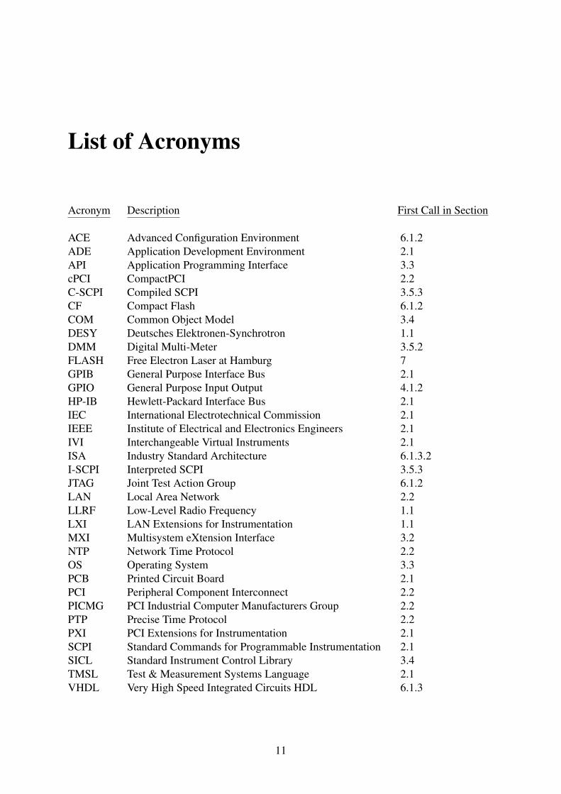
ACE Advanced Configuration Environment 6.1.2ADE Application Development Environment 2.1API Application Programming Interface 3.3cPCI CompactPCI 2.2C-SCPI Compiled SCPI 3.5.3CF Compact Flash 6.1.2COM Common Object Model 3.4DESY Deutsches Elektronen-Synchrotron 1.1DMM Digital Multi-Meter 3.5.2FLASH Free Electron Laser at Hamburg 7GPIB General Purpose Interface Bus 2.1GPIO General Purpose Input Output 4.1.2HP-IB Hewlett-Packard Interface Bus 2.1IEC International Electrotechnical Commission 2.1IEEE Institute of Electrical and Electronics Engineers 2.1IVI Interchangeable Virtual Instruments 2.1ISA Industry Standard Architecture 6.1.3.2I-SCPI Interpreted SCPI 3.5.3JTAG Joint Test Action Group 6.1.2LAN Local Area Network 2.2LLRF Low-Level Radio Frequency 1.1LXI LAN Extensions for Instrumentation 1.1MXI Multisystem eXtension Interface 3.2NTP Network Time Protocol 2.2OS Operating System 3.3PCB Printed Circuit Board 2.1PCI Peripheral Component Interconnect 2.2PICMG PCI Industrial Computer Manufacturers Group 2.2PTP Precise Time Protocol 2.2PXI PCI Extensions for Instrumentation 2.1SCPI Standard Commands for Programmable Instrumentation 2.1SICL Standard Instrument Control Library 3.4TMSL Test & Measurement Systems Language 2.1VHDL Very High Speed Integrated Circuits HDL 6.1.3
11
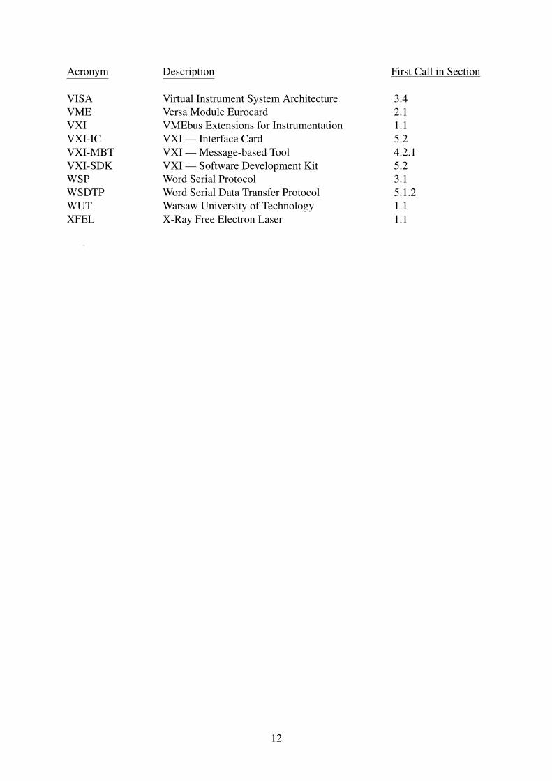
Acronym Description First Call in Section
VISA Virtual Instrument System Architecture 3.4VME Versa Module Eurocard 2.1VXI VMEbus Extensions for Instrumentation 1.1VXI-IC VXI — Interface Card 5.2VXI-MBT VXI — Message-based Tool 4.2.1VXI-SDK VXI — Software Development Kit 5.2WSP Word Serial Protocol 3.1WSDTP Word Serial Data Transfer Protocol 5.1.2WUT Warsaw University of Technology 1.1XFEL X-Ray Free Electron Laser 1.1
.
12
1
Introduction
1.1 Thesis Origin
In 2004, the author of the dissertation joined the Research Group on Automatic Test Sys-tems led by Prof. Konrad Hejn at Warsaw University of Technology (WUT). Among otheractivities, the Group is involved in research of new technologies in VMEbus Extensions forInstrumentation (VXI) systems. Since 1990 the Group has put much effort into popularizationof the VXI standard in the university environment. Several VXI devices were designed and de-veloped in the past but there is still a need for some new tools and devices compliant to the VXIstandard that would support the didactic branch of the Group’s activities.
Since 2004 the author of the dissertation has been collaborating with the Deutches Elektro-nen-Synchrotron (DESY) in Hamburg, Germany [1] within the scope of the international X-rayFree Electron Laser (XFEL) project [2]. This is a new European project, which started in 2007.XFEL is a linear electron accelerator which will produce high intensity X-rays for materials andbiological research. The author has been working in the international team which built a LowLevel Radio Frequency (LLRF) control system for the existing, prototype Free Electron Laserat Hamburg (FLASH) accelerator [3]. The existing LLRF system is a kind of a measurementand control system [4]. It took advantage of world-wide technologies and was enhanced byhigh-tech solution customized to the FLASH accelerator environment. New technologies mustbe involved in construction of the LLRF control system for XFEL, because it is meant to workfor the next 20 years starting in year 2013. The author is involved in development of the LLRFsystem, particularly in its digital part.
The activities of the Warsaw and DESY groups converged at the time that led to the formu-lation of this thesis in 2004. Most of the results achieved in this work are addressed to smalllaboratories such as the Warsaw Group, yet they are useful for the bigger laboratories such asDESY. Thus, the results of the dissertation could contribute to the control of the XFEL, sincethey show how to utilize advantages of the VXI standard, and, in the future, of the LXI (LANeXtension for Instrumentation) standard, for a LLRF system. The English language presenta-tion of this work is motivated by the international audience to which it is addressed.
13

1.2 Dissertation Contents
This work is divided into 8 chapters and several appendices.
Chapter 1 presents the origin of the dissertation and some technical issues such as a glos-sary and editorial remarks.
Chapter 2 gives historical overview of world-wide computer technologies and standardsrelevant for instrumentation. Special attention is put on the VXI standard and SCPI program-ming techniques since they are the key points for this work.
Chapter 3 describes, layer by layer, hardware and software components that could be dis-tinguished in a VXI system. The detailed understanding of the software techniques used fordevelopment of device drivers is crucial for the new development method proposed in this work.
Chapter 4 exhibits problems connected with development of VXI message-based devicesin small laboratories and formulates the dissertation thesis. It also contains goals and require-ments that must be met in order to fulfill these goals.
Chapter 5 describes the model of the designed tool and proposes a new methodology foreffective development of VXI message-based devices.
Chapter 6 includes implementation issues for the tool. It briefly describes the design ofthe tool, realization of the hardware board, firmware implementation and associated software.More attention is put on unique technical solutions that allowed meeting the assumed require-ments.
Chapter 7 presents the application of the tool to the LLRF control system for acceleratingmodules based on the SIMCON 3.1 board. This application proves the effectiveness of the tool.It can be also treated as a tutorial for using the tool and the methodology proposed in chapter 5.
Chapter 8 summarizes the entire work, uncovers weak points of the tool and explains ideasfor its improvement. This chapter also suggests the modifications necessary to built similarlyeffective tool for the development of LXI message-based devices.
1.3 Glossary
Several terms are defined in this section which have special meaning important for properunderstanding of the dissertation.
VXI controller is in charge of bus communication and device management. It is locatedin a slot 0 of the VXI chassis. It controls the data flow, performs addressing and other busmanagement functions such as bus arbitration, interrupts acknowledgment, etc. The VXI sys-tem controller is usually a resource manager, detecting active devices and assigning systemresources to them.
VXI device, also simply called a device, is a component of a system that does not func-tion as the system controller but typically exchanges data with the VXI controller, either asbinary blocks or text messages. The VXI device consists of a VXI interface and device specific
14

functions.Tool, also called VXI-MBT, is the subject of this work. The word tool is used in chapters
from 1 to 4. The VXI-MBT is used starting from chapter 4.User electronics or user device is a piece of specific electronic equipment that is adapted
to the VXI/SCPI standards using the tool.Control software is used to control a VXI system. This software is located in a VXI
embedded computer, or on a remote, stand-alone, personal computer.VXI configuration registers are obligatory for each VXI device. They are used by a VXI
controller for identification of a device in a VXI system.VXI communication registers are obligatory in each VXI message-based device. They
are used for implementation of the obligatory Word Serial Protocol and other optional commu-nication protocols.
Working registers are completely device dependent. They are used to control device func-tionality and to report its state.
SCPI message is a text string compliant with the IEEE 488.2 syntax that is exchangedbetween control software and a VXI device. It is either a command or a query sent fromthe control software to a VXI device, or a response that is sent from a VXI device to the controlsoftware.
1.4 Editorial Remarks
In order to emphasize some keywords in the text, a different typefaces were used with respectto the regular text:
• the Typewriter style is used for SPCI messages, Common Commands and C func-tions,
• the Slanted style is used for keywords indicating components presented in figures, andspecial components defined by standards documentation,
• the Italic style is used for signals and register names.
The document contains a large number of acronyms. The full name of each acronym is writ-ten intentionally once, when it appears for the first time in the text. The list of acronyms locatedat the beginning of the document is meant to remind the reader of some of them. Acronyms incommon use in measurement and control system circles might not be included.
15

16

2
Industrial Standards for Instrumentation— Historical Overview
The evolution of measurement and control systems has been prompted by rapid developmentof computer technologies for more than 30 years. It has aimed at building faster, automatedand integrated systems to provide to users with more precise information and to give morecontrol of the explored objects. Computer manufacturers and software vendors proposed manyideas, approaches, techniques and methodologies. Their usability was verified every day inpractice by a large number of developers and users around the world. Only solutions commonlyaccepted by the market passed the exam and finally became commercial standards. The strongcompetition eliminated customized, expensive solutions from the market. Some of the mostpopular commercial standards were converted into international standards, but only a few ofthem were adopted by the instrumentation industry as a basis for measurement extensions.The most popular international standards have dictated trends in the instrumentation industryfor decades.
This section presents the past evolution of some of the computer technologies and standardsand of their adoption by instrumentation industry. Figure 2.1 shows dependencies graph ofthem and provides historical overview.
2.1 From IEEE 488 to Modern VXI Systems
The first standard globally used in measurement and control systems was IEEE 488, developedby the Institute of Electrical and Electronics Engineers (IEEE) in 1975. It defined a digitalbus which was originally developed by Hewlett-Packard and called Hewlett-Packard InterfaceBus (HP-IB) [5]. It is a simple and fully digital bus which permits easy integration of stand-alone measurement devices into a system and simultaneously exempts system developers fromcumbersome communication at the register level. The interface quickly became very popularin the instrumentation industry. In 1975 the IEEE committee gave it its present number andrenamed it to General Purpose Interface Bus (GPIB) .
17

VERSAbus 1979Motorola
VMEBus 1981Motorola, Mostek, Signetics
ANSI/VITA-1 1994VME64
IEEE 488.21987
VXIbus 1987Tektronix, Wavetek,
Colorado Data Systems, HP, Racal Dana
VXI-1 IEEE 1155-1992
Rev. 1.4
VXI-1 1998Rev. 2.0
IEEE 4881975
IEEE 488.11987
SCPIRev. 1990
SCPIRev. 1999
VXI-1 2003Rev. 3.0
IVI Foundation1998
IVI Foundation2002
VXIplug&play1993
ANSI/IEEE 1014, IEC 821 1987
ANSI/VITA-1.1 1997VME64x
VMEbus, Rev. C
IEEE 1101.1,10,11Eurocard
PICMG 2.0 - 1995Rev. 3.0
CompactPCI
PXI – 1997Rev. 1
PCI 1992Rev. 1.0
PCIe 1.0 - 2004PCI-SIG
PXI-5 - 2005 PXI Express
Ethernet – 1975Xerox
IEEE 1588 2002
LXI 2005Rev.1
PCI 1995Rev. 2.1
PXI-1 – 2004Rev. 2.2
VXIplug&play
PXI
PXI-2 – 2008Rev. 2.3
PCIe 2.0 -2006
IEEE 802.3 – 1985Ethernet
LXI 2007Rev.1.2
Figure 2.1: Diagram of Standards Evolution and Dependencies
The IEEE 488 standard indeed assures that messages have been accurately transfered be-tween two or more devices in a system, but does not guarantee that each device will interpretproperly all possible messages sent to it, or will properly create all necessary responses. A widelatitude of interface capability is permitted within the scope of this standard which often resultsin operational incompatibility among interconnected devices. Thus, in 1987, the IEEE 488standard was revised and upgraded to ANSI/IEEE Std 488.1-1987 — IEEE Standard DigitalInterface for Programmable Instrumentation [6]. In the same year the IEEE 488.2 was launched[7]. The IEEE 488.2 standard arose from the need for a common messages format for devicecommunication. It is supplementary to IEEE 488.1 and brings into a device some artificial in-telligence. It defines syntax of messages, introduces a set of Common Commands, and definesmessage exchange protocol and a message exchange control interface. The message exchangecontrol interface is defined as a state machine that reacts on external events such as incomingmessages, response requests, and measurement device actions. It prevents device deadlocksand loss of messages as well as managing input and output queues of messages and responses,and reporting protocol errors.
Compared to present computer buses, GPIB was rather primitive. There was only onecontroller in a system. The GPIB bus was 8-bit wide and its data multiplexed with addresses.
18

The maximum data transfer rate on the bus was 1MB/s for standard communication protocol(handshake) or up to 8MB/s for HS488 (high-speed handshake developed by National Instru-ments in 1993)[8]. But GPIB had one important advantage at that time. The digital circuitresponsible for bus interface was fairly simple and several integrated circuits implementingthe GPIB interface appeared on the market. Such a single chip interface was very convenient touse for development of GPIB devices. Developers focused on sending and receiving messagesinstead of signal control or transmission flow control. But soon new and faster buses appearedon the market, offering alternative interfaces for applications with higher bandwidth.
In parallel to IEEE 488.x, the computer communication buses were evolving, too. AlthoughGPIB has been very popular and easy to implement in measurement devices, the limited datatransfer rate on the bus became a real issue. The GPIB transfer of 1MB/s was good enough inmost non-electronic applications, but measurement and control systems were getting more andmore complex, and more data was being transfered on the bus. Developers of measurementand control systems started looking for communication buses with higher throughput. In orderto avoid expensive development of custom communication buses, the most popular existingcomputer buses became points of interest. A typical computer bus provides a well tested com-munication medium with optional interrupts and arbitration mechanisms. But measurementand control systems require in addition precise synchronization tools. Therefore, the computerbus standards had to be extended by precise hardware or/and software synchronization mech-anisms. The following measurement standards were developed as extensions of computer busstandards:
• VME Extensions for Instrumentation - VXI
• PCI Extensions for Instrumentation - PXI
• LAN Extensions for Instrumentation - LXI
In 1979 Motorola developed their new processor 68000. In addition, they built an asyn-chronous bus in order to support the processor. The first version of this parallel, asynchronousbus was named VERSAbus [9]. The bus quickly became popular among computer manufac-turers. The engineers from Motorola-Europe division added to it mechanical standards thatbecame later international standards. They defined standard racks, chassis, and Printed CircuitBoard (PCB) form factors, formerly named by the International Electrotechnical Commissionas IEC 297-3 and currently known as IEC 60297-3-101 [10]; connectors IEC 603-2 currentlyknown as IEC 60603-2 [11] and marked as DIN 41612. The outcome of these mechanical andelectrical standards was VERSAbus-E (VERSAmodule Eurocard bus). In October 1981, Mo-torola, Mostek and Signetics announced their support of VERSAbus-E and gave it its presentname Versa Module Eurocard (VME) bus. The VME bus became a very popular standard andin 1987 the revision C was released, officially standardized by IEC as IEC 821 VME bus andby IEEE as ANSI/IEEE 1014.
19

In 1987, engineers from the biggest manufacturers of measurement devices such as Tek-tronix, Wavetek, Colorado Data Systems, HP, and Racal Dana founded a committee for specifi-cation of an open architecture standard for instrumentation based on the VME bus and Eurocardstandards, and compatible with IEEE 488.2-1987 devices. They agreed to support a modularinstrumentation architecture named VXI bus. In the next years other companies joined the col-laboration and finally formed the VXI Consortium. After several workshops and technicalmeetings the main specification with four revisions was created in order to insure completedocumentation of the VXI standard. In 1992, the VXI-1 Revision 1.4 specification was ap-proved by IEEE with the number 1155-1992. Since then two new revisions have been released,mainly due to evolution of the VME bus. In 1994, IEEE released a new version of the VMEbus specification named ANSI/VITA 1-1994, known as VME64 [12]. The new standard de-fined multiplexing of address and data lines for 64-bit addresses and 64-bit data transmissionon the VME bus. It also defined 5-row, 160-pin P1 and P2 connectors where the outer rowswere reserved for later releases. The D64 data transmission and RETRY* line were incorpo-rated in revision 2 of the VXI standard and the revised revision VXI-1 Rev. 2.1 was releasedin 1998 [13]. And again, in 1997, ANSI and the IEEE released an update of the VME bus un-der ANSI/VITA-1.1, commonly named VME64x or VME64 Extensions. This version definesthe meaning of pins on rows d and z of the 5-row connectors P1 and P2. It also defined twotransmission protocols 2eVME and 2eSST. The latter one increased data transfer rate on VMEto 320MB/s [14]. The last version of the VXI standard released in 2003 under number VXI-1Rev. 3.0 [15] incorporated A64 addressing mode from VME64 and 2eVME transfer protocolfrom VME64x which increased the data transfer rate on VME bus up to 160MB/s.
With VXI and IEEE 488.2 standards becoming more and more popular in measurementand control systems, the need for software standardization became an important issue. The firstattempt was to unify syntax of data exchanged between control software and devices. In 1989,Hewlett-Packard introduced a device control technique based on ASCII codes and named itTest & Measurement Systems Language (TMSL) . In the same year TMSL was verified bya committee of leading measurement device manufacturers which founded the SCPI Consor-tium and developed SCPI — a set of Standard Commands for Programmable Instrumentation[16], [17]. SCPI has taken syntax from IEEE 488.2, defined sets of commands based on a stan-dardized model of a measurement device, and determined the semantic of commands. Althoughthe SCPI specification doesn’t say explicitly that it defines command semantics, the semanticalmeaning of messages is mentioned several times in the specification. Unlike IEEE488.2, SCPIis independent of the communication interface — it is strictly a software standard. SCPI mes-sages can be exchanged between devices using RS232, RS482, Ethernet, GPIB or VXI bus.SCPI became very popular in VXI systems, especially for message-based devices. The bigadvantage of SCPI is that it is a purely textual set of commands and can be implemented onany computer platform and in any programming language. Nowadays, SCPI is also used inApplication Development Environments (ADE) such as LabWindows, LabVIEW or VEE Pro.
20
Although SCPI is still in use and yearly updates are released, it has never become an interna-tional standard, but quite often in the literature it is called a standard — a commercial standard.
Although SCPI simplified device programming, it didn’t solve the problem of how to writea device driver which can be easily incorporated in a user applications for measurement andcontrol systems. That was particularly important for devices programmed at register level, be-cause such device must be provided with an associated driver in order to keep users away fromthe details of programming device working registers. The software developers were strug-gling with problems of how to write programs for measurement devices which can be portableacross different computer platforms, can operate with software from other vendors, or even,how the same software can be used for devices from different vendors. A first attempt at de-vice driver standardization was made in 1993 when the VXIplug&play Alliance was formed. Itproposed common standards and practices for software development based on well defined andcomplete system frameworks. This organization was primarily founded to support VXI mea-surement and control systems, but the VXIplug&play specification went beyond the scope ofVXI and offered interoperability for both hardware and software on various computer platforms[18].
But some software vendors noticed a need for further standardization of device drivers. In1998, the IVI Foundation was formed and proposed Interchangeable Virtual Instrument drivers.IVI offered a new architecture of the device drivers that supported interchangeability of devicesand drivers from various vendors [19]. Interchangeability means that the same device drivercan be used for devices of the same class from different vendors. The idea of interchangeabledrivers quickly became very popular among software developers, instrument vendors, end-users, and system integrators. In 2002, the VXIplug&play Alliance was incorporated intothe IVI Foundation and part of the VXIplug&play specification was utilized. In the same yearthe SCPI Consortium also became a part of IVI Foundation. The activity of SCPI continuesand annual meetings on SCPI specification updates are organized under supervision of the IVIFoundation.
2.2 PXI and LXI Standards
The success of the VXI standard stimulated developers to adapt other computer communicationbuses to measurement and control systems. In 1990, the Intel company started development ofa communication bus for personal computers — Peripheral Component Interconnect. PCI buswas meant for attaching peripheral devices to a computer motherboard. In 1992, revision 1.0of the PCI specification was released. In the next years new revisions completely defined PCIincluding connectors, motherboard slots, configuration procedures, etc. Over one decade en-hancements to PCI led to an improvement of transmission speed up to 266 MB/s and doublingof the bus width to 64-bit.
The popularity of the VME standard inspired companies to built cardcage versions of PCI
21

for instrumentation. In order to create cardcage devices as in VXI systems, the CompactPCI(cPCI) standard was introduced in 1992. It used the Eurocard standard and defined a newbackplane with the PCI bus as a communication core. cPCI is an open specification supportedby the PCI Industrial Computer Manufacturers Group (PICMG) [20]. PICMG was founded bycompanies that make use of PCI in embedded applications. The cPCI specification was releasedin 1995 under name PICMG 2.0. In the following years PICMG issued several subsidiaryspecifications PICMG 2.x which defined hot swap capability, PCI Mezzanine Card (PMC),system management, electronic keying and application of serial communication standards onthe backplane.
The cPCI standard defined five connectors on the backplane. Connectors J1 and J2 are usedfor PCI implementation and the other connectors contain general purpose I/O pins which areused for implementation of subsidiary PICMG 2.x specifications.
Analogous to the VXI standard, which grew up on a VME basis, the PXI standard wasdeveloped based on cPCI. In 1997, the first revision of the PXI specification was released bythe PXI System Alliance (PXISA). Some of pins on the J2 connector reserved in cPCI wereadapted in PXI. The cPCI bus was extended by a 10MHz system clock, eight shared triggerlines, and low-skew trigger lines in a star topology. PXI also defines 13 lines for a local busbetween two adjacent modules. The PXI standard doesn’t define message-based devices. MostPXI devices are register-based with obligatory registers defined by the PCI standard. A disad-vantage of PXI is the lack of shielding definition in the specification. This is an important issuefor measurement devices since Electromagnetic Interference (EMI) from digital cards may sig-nificantly influences some of the sensitive analogue cards, and limits their resolution to 10–12bits. The PXI standard also refers to the VXIplug&play specification and defines extensionsfor integration of the communication library with PXI modules. PXI also defines interfaces toVXI and GPIB.
In 2004, Intel introduced a new computer expansion card interface named PCI Express,abbreviated as PCIe [21]. The specification of this standard is maintained by the PCI SpecialInterest Group (PCISIG). PCIe defined links for serial communication in order to replace PCIand Accelerated Graphic Port (AGP) computer interfaces. PCIe consists of serial, full-duplexlinks called lanes. Each PCIe slot can have up to 32 lanes, connecting up to two devices at bothends. For communication of more devices a special PCIe switch is required. Each lane cantransfer up to 250MB/s in each direction. PCIe 2.0, released in 2006, doubles the data rate.
Again, the computer standard was adapted to measurement and control systems. First ofall, the PCIe standard was incorporated in cPCI and then, in 2005, PXISA released the PXI-5specification, which includes PCIe [22]. The PXI Express defined a new connector with dif-ferential pairs for fast communication. In PXI Express chassis the PXI-1 standard is allowedwhich means that hybrid chassis may contain slots for traditional PXI and new PXIe modules.PXIe also uses differential lines for triggers, clocks, and serial communication interconnectionsbetween modules.
22

Another very popular computer interface is Ethernet. Nowadays, almost every computeror measurement device has an Ethernet connector. Ethernet was originally developed by engi-neers from Xerox in 1975. After a few years of experimentation, this packet switched protocolwas used for networking of computers in Local Area Networks (LANs) . In 1979, Ethernet wasstandardized as a 10Mb/s communication protocol with 48-bit destination addresses. It wasalso approved by IEEE under the number 802.3 in 1985 [23]. There are several physical im-plementations of Ethernet which are defined in IEEE 802.x specifications. Ethernet is the mostdynamically evolving standard with several versions; the maximum Ethernet bit rate is now10Gb/s on various physical communication media.
Recently, Ethernet has become the most popular standard for computer communication dueto cheap mass production, so it is hardly surprising that there have been attempts to use Ethernetin measurement and control systems. The biggest problem of using standard Ethernet in mea-surement and control systems has been the uncertainty of the packet delivery time. Dependingon traffic, the delivery time could vary by several milliseconds and sometimes packets mighteven be lost. The main synchronization requirements of measurement and control systems can’tbe fulfilled.
This problem was solved by the new IEEE 1588 standard introduced in 2002. IEEE 1588defined a precise clock synchronization protocol for networked measurement and control sys-tems. This protocol, also called Precision Time Protocol (PTP), guarantees synchronizationin the submicrosecond range, better than 100ns across an Ethernet network, if the subnet formeasurement and control system is carefully designed. In this case special Ethernet adaptersand switches with hardware implementation of IEEE 1588 are required for the precision men-tioned above [24]. This standard has much better accuracy than similar, existing Network TimeProtocol (NTP). IEEE 1588 is also useful for applications where Global Positioning System(GPS) is not available or the cost of a GPS receiver is an issue [25].
The IEEE 1588 standard stimulated engineers to develop the next generation of standard forinstrumentation named LXI [26]. In 2005, Agilent Technologies and VXI Technology compa-nies founded the LXI Consortium. The main goal of the consortium was to develop a newstandard based on Ethernet and synchronized by PTP. The main advantage of LXI is incorpo-ration of existing computer networks which allows building a measurement and control systemdistributed across a large geographical area without any additional hardware/software cost forinterfaces. Any measurement device that has a LAN interface may become a part of the sys-tem; any computer that is connected to the same network can control the system. LXI definesstand-alone devices with small and flexible housings. An intention of LXI housing is the possi-bility of installation in 19 inch racks. The LXI device doesn’t have a front panel, yet a WWWinterface is required. Each LXI device should also provide an IVI driver with minimum func-tionality defined by the IVI specification. It is also recommended that LXI devices supportSCPI messaging.
LXI also defines an optional hardware trigger bus for device synchronization when several
23

nanosecond precision is required. But the trigger bus in a device requires another connectordedicated to the synchronization signals and separate cabling must be assembled.
With several adapters available on the market, such as VXI/LAN or GPIB/LAN, other mea-surement devices or systems may be integrated with LXI.
2.3 Summary — Why VXI Systems?
Several measurement standards, computer interfaces, programming languages, software tech-niques and tools now exist on the market. Although almost 35 years has passed since the firstcomputer measurement and control systems, neither universal bus standards nor universal soft-ware has been developed. The design of a user measurement and control system depends onseveral aspects which must be taken into account, such as the purpose of the system, the archi-tecture, size, power consumption, resolution and of course the price. None of the standards andtechnologies is able to fulfill any combination of these aspects for every solution.
This chapter presented a number of the standards which have played a significant role inthe development of today’s measurement and control systems. Many of them became de iure
standards approved by international organizations such as IEEE or IEC, e.g. VXI, IEEE 488.2,Eurocard, Ethernet, etc. These are hard, invariant standards; manufacturers must follow themstrictly in order to build compliant devices. If a new revision of a particular standard is released,the organization usually takes care of backward compatibility, so that legacy devices can stillwork in modernized systems. All others are de facto standards (industrial standards), usu-ally developed by organizations, consortia, committees, alliances of manufacturers, e.g. SCPI,IVI, VXIplug&play, PXI, LXI, etc. The existence of these standards depends on market eco-nomics. They are supported when there is demand for devices based on them, and may vanishif the companies which created them disappear. A new revision doesn’t need to be backwardcompatible if it is not profitable.
Also, combinations of different standards are of benefit to the customers. For example,the de iure VXI and IEEE 488.2 standards profit from message-based devices which talk toeach other using the de facto SCPI standard. As long as the VXI standard is used, SCPI willbe used — although SCPI is also used in conjunction with other standards. The market hasverified the usability of the VXI standard; there are a number of companies which have beendeveloping VXI devices for many years. One can expect that the new, de facto LXI standardwill soon become an international standard due to its being based on Ethernet (IEEE 802.3),synchronization protocol (IEEE 1588), and its rapidly growing popularity.
24

3
Modern VXI/SCPI Measurement andControl Systems — State of the Art
VXI systems have been evolving for 21 years. Although three revisions have been released untilnow, no major modifications to the standard were introduced with respect to the first revision.New revisions of the VXI standard have mainly taken advantage of VME bus improvements.In case of software for VXI systems, no international standard has been established. A hugenumber of software techniques have been used for the control of VXI systems. Most of themwere developed for custom applications and are not used any more. A few of the softwaretechniques mentioned in chapter 2 are still being used, and they became the industrial standardscommonly used in modern VXI systems. This chapter presents the most popular softwarestandards and techniques, and their relationship to hardware.
Figure 3.1 presents the layering of hardware and software in modern VXI/SCPI systems.There are a variety of hardware components and software techniques which users may want toincorporate in their VXI systems. Several aspects must be taken into account before the systemcan be built. A typical VXI system will include neither all of these layers nor all of the computerinterfaces presented in figure 3.1. The following sections briefly describe each layer, its role inthe VXI system, and the benefits it provides.
3.1 VXI Devices
A VXI device is a piece of electronics which performs specific functions in a measurement andcontrol system. Physically the device takes the form of an electronic module which is able tooperate only in a VXI chassis. One VXI module may contain one or more VXI devices, andmay occupy one or more slots of the VXI chassis. Each VXI device contains a VXI interfaceand one or more optional interfaces on a front panel, e.g. high quality analog I/O. The VXIstandard defines four types of devices: register-based, message-based, memory, and extendeddevices. But only two of them have become very popular: message-based and register-based.
Register-based devices are popular due to a simple construction similar to VME devices.
25

Configuration Registers
Windows, HP-UX Linux, WxWorks
Working RegistersDevice Functions
Binary Data ASCII Codes
Binary Data
Register-based Device
SCPI Processor
Configuration RegistersCommunication Registers
I/O Libraries (SICL/VISA)
User Program
VXIplug&play
Working RegistersDevice Functions
Binary Data
ASCII Codes
C-SCPI I-SCPI
IVI
Device Driver
Device Driver
Binary Data
VXIplug&play IVI
Message-based Device
ASCII Codes
SCPI Processor
1. Devices
6. Programming Languages & ADE
5. Device Drivers
4. I/O Libraries
MessageExchange
Control
ASCII Codes
VXI Chassis Controller 2. Controllers
VXLink GPIB MXI USB RS-232 FireWire 3. Digital Interfaces
VXI Bus
LANVXI Bridge
Figure 3.1: Architecture of a Modern VXI System
The design of such a device is relatively easy as it must be only furnished with a few configu-ration registers (VXI obligatory registers) and several device dependent working registers forits operation (similar to VME devices), as presented in figure 3.1. The artificial intelligenceneeded to control the device is located in higher layers of the control software.
Register-based devices enable direct access to working registers from the VXI bus. The soft-ware controls such devices by reading and writing binary data to working registers. Writingeffective control software for a register-based device requires from the programmer detailedknowledge of the meaning of each bit in each working register. In addition, good knowledge ofdevice behavior is required, because the ordering of reads and writes is also important. Softwarewritten for one register-based device in a specific application usually doesn’t match to other ap-plications. In many cases manufacturers of register-based devices provide basic software fordevice operation, called in this dissertation a device driver. Such a driver hides the complexityof working register programming and offers a more general, higher level software interfacewhich can be used in several user applications. But the device driver is in many cases a customapproach and it is not portable to different development platforms or applications. An attemptat device driver standardization was made by the VXIplug&play Alliance. Further standard-ization was done by the IVI Foundation, as described in this chapter. The left part of figure
26

3.1 presents the complete hardware and software setup for register-based devices with differentsort of device drivers.
Message-based devices exchange data with control software using a communication pro-tocol. Instead of the binary data for register-based devices, the communication protocol trans-ports messages between a message-based device and control software. Each message-baseddevice should implement at least one communication protocol. The device should includeenough local intelligence to interpret and decode messages as well as to format and send backresponses. In addition to the configuration registers, the VXI message-based device shouldcontain a set of communication registers for the message transport. The VXI standard definesfor the message-based device only one obligatory communication protocol, called Word SerialProtocol (WSP). A few obligatory WSP commands should be implemented for basic configu-ration of message-based devices, see [15] section C.2.4. In addition, the VXI standard definesoptional conformance of message-based devices to the IEEE 488.2 standard. This rule impliesthat the message-based devices may exchange messages based on the IEEE 488.2 syntax, andaccording to the message exchange protocol, also defined in the IEEE 488.2 standard. Thus,SCPI messaging can be implemented on message-based devices compliant to IEEE 488.2. Al-though the VXI standard doesn’t specify the use of SCPI for message-based devices, SCPIis based on the IEEE 488.2 syntax and it is natural to use it. Nowadays, almost every VXImessage-based device is programmed by using SCPI.
Communication by messages requires additional processing power in the device itself.The received SCPI commands must be somehow interpreted and executed, and the responsesmust be formatted in a standard manner. Such complex operations require a processor on boardand some memory for buffering the input and output messages. The SCPI command parserand response formatter comprise a SCPI processor. The set of execution routines associatedwith the SCPI commands form a device driver. The SCPI processor and the device driver forma so-called SCPI driver. The idea of message-based devices is presented on the right side offigure 3.1.
3.2 VXI Controllers
The VXI controller performs two roles in a VXI chassis; it is responsible for VXI bus control,and for resources management. As a bus controller, it arbitrates the traffic on the bus, controlsthe interrupt priority handling scheme, generates triggers, and communicates with external sys-tems or computers. The resource manager performs VXI subsystem self-configuration. Thisincludes device identification, dynamic address assignment, address space configuration, inter-rupts enabling, handlers assignment, triggers signal assignment, etc.
The VXI controller is a module installed in slot 0 of the VXI chassis. It may be equippedwith different types of digital interface on a front panel for communication with the con-trol software. There are several controllers with computer interfaces on the market, such as
27

the Agilent E8491B with FireWire [27] and the VXI Technology controller with a USB in-terface [28]. Some of the controllers have interfaces to other measurement buses such asthe Agilent E1406A [29] with GPIB, Agilent E1482B with Multisystem Extension Interface(MXI) [30][31], or the VXI Technology EX2500 [32] with an interface to LXI [26]. NationalInstruments offers a large family of slot 0 VXIpc embedded computers [33]. They occupy 1,2 or 3 slots depending on features inside such as hard drives, CD-ROM, PCI slots, etc. Un-fortunately, the embedded controllers are usually expensive and they are only used in specificsituations where external computers cannot be used. In addition, such embedded computersdissipate a lot of power and emit electromagnetic noise in the VXI chassis.
The embedded computer usually hosts all software from layer 3 to 6, as presented in figure3.1. In such cases the user application is built in a client-server architecture [34]. The clientapplication located on a remote computer communicates over LAN with a server application inthe VXI embedded computer. In VXI systems managed by simple controllers with computerinterfaces all software from layers 4 to 6 is located in a remote computer. Hence, there is noneed to build a distributed user application, however it is still possible, if required.
A VXI controller talks to register-based devices by reads and writes either to the configu-ration or working registers. In case of the message-based devices the controller talks to themusing WSP commands.
3.3 Digital Interfaces
A digital interface provides a communication channel between the VXI system and controlsoftware running on a user computer. The communication channel consists at least of oneor more hardware components and communication software in the computer. The hardwarecomponents are cables, adapters, computer cards, and/or bus adapters. All VXI controllersmentioned in the previous section can be physically connected through one of the front panelinterfaces. In case of embedded computers a specialized VXI bridge connects to the VXI buson one side and to the local processor bus on the other.
Every digital interface in a computer must include an associated interface driver so that itis visible to the Operating System (OS) and the control software can access the hardware con-nected to it. Digital interface drivers export Application Programming Interface (API) func-tions which are used by the control software to establish communication with external devicesconnected to the interface.
The user can write a program which communicates with a VXI system connected to a com-puter by calling the interface driver API. This approach provides very fast communication withthe hardware, but is an inefficient programming style from the point of view of software re-usability, especially for measurement and control systems. Almost every interface driver hasdifferent API functions. If the user wants to switch his system from one interface, such asGPIB, to another, such as Ethernet, the program must be almost completely rewritten because
28

GPIB LAN
User Program A
Operating System
Work Station or PC or Embedded Computer
User Program B
Device A Device A
6. Programming Languages & ADE
3. Digital Interfaces
1. VXI Device
E1406A EX2500
VXI Bus VXI Bus
2. Controllers
Figure 3.2: Communication with VXI Devices Through Various Digital Interfaces
API of the interface drivers is different. That situation is presented in figure 3.2. This methodof software development for measurement and control systems is now employed very rarely.
3.4 I/O Libraries
The access to a VXI system through various digital interfaces can be unified using I/O libraries.From one side they handle the details of a particular OS driver for hardware interface; onthe other side, they provide a unified software interface to higher levels of the control software.An example of interconnectivity is presented in figure 3.3. The same measurement and controlsystem is connected in one case through a GPIB interface, and in the other through Ethernet.In both cases the same user program is used to operate the measurement and control system.
GPIB LAN
User Program A
Operating System
Work Station or PC or Embedded Computer
User Program A
Device A Device A
6. Programming Languages & ADE
3. Digital Interfaces
1. VXI Device
E1406A EX2500
VXI Bus VXI Bus
2. Controllers
VISA/SICL 4. I/O Libraries
Figure 3.3: Interconnectivity of VISA library
29

The first I/O libraries were introduced by Hewlett-Packard and were named the StandardInstrument Control Library (SICL). Currently, SICL is maintained by Agilent. SICL is a soft-ware library which exports the API to higher software layers [35]. It is a bridge between digitalinterface drivers and higher software layers. The library is portable to different OS such asWindows and HP-UNIX, and was recently ported to Red Hat Linux by Test & MeasurementSystems Inc. [36]. SICL implemented many functions typical for several interfaces such asGPIB, VXI, RS-232, LAN and USB. The Virtual Instrument System Architecture (VISA) isa successor to SICL and is an industry standard approved by most measurement and controlsystems manufacturers. VISA took advantage of all software implemented in SICL and it wasdesigned according to the VXIplug&play System Alliance specification [37].
The VISA/SICL library gives from the user point of view a high level of interconnectivity,because the same measurement system may be connected to the computer through differentdigital interfaces and the user program needn’t be changed. The same software interface isprovided by the SICL/VISA library for a user application regardless of the hardware interface.The VISA library is recommended instead of SICL for the development of new software.
The software interface of the VISA library consists of several sets of universal communica-tion functions. The variety of functions enables users to develop programs taking into accountspeed, simplicity and operability. The Formatted I/O or Non-Formatted I/O functions usuallyare used for message-based devices because they are used to transfer ASCII strings. The High-level, Low-level and Memory I/O functions are used for register-based devices because theyprovide simple read and write functions with varying levels of automation. The user can choosebetween coding simplicity (High-level and Memory I/O functions) with slower execution, orspeed (Low-Level functions) with more complex coding. In addition, VISA/SICL providesfunctions for event detection in a VXI system, such as interrupts, triggers, service requests,VXI system failures, I/O operation completion, etc.
The VISA library is released in two versions VISA API and VISA COM. VISA API isoptimized for C/C++ language as well as for Visual Basic 6 and other software environmentswhich can call dynamic Windows libraries. VISA COM is an object version of the VISAlibrary which makes the library independent of programming language [38]. It utilizes the Mi-crosoft Common Object Model (COM) . COM technology is an object-oriented representationof the VISA API interface that is perfect for Visual Basic 6, Visual Basic .NET and C# as wellas different ADEs such as Agilent VEE Pro or NI LabVIEW. A handicap of VISA COM isthat it is a commercial solution based on the COM technology which was created and drivenby Microsoft, thus, it can only work under the Windows OS.
3.5 Drivers for VXI Devices
The I/O libraries provide interconnectivity for different digital interfaces. Using I/O libraries,the connection to the VXI devices is established, but the communication protocol is not provided.
30

Instrument Driver(Functional Body)
Interactive Developer Interface
Programmatic Developer Interface
Subroutine Interface VISA I/O Interface
User Program
Figure 3.4: VXIPlug&Play Driver Concept
The higher software levels must take care of communication protocol handling. This can bedone either in a user program or by a dedicated driver. The preferable method is a device driver.The complex device programming at the working register level is encapsulated in a driverprovided by the vendor together with the device. The intention of the driver is to simplifydevice control from user programs, especially for register-based devices. The device driverreleases the user from learning details of the device working registers. Different programmingapproaches for device drivers enable various levels of hardware independence, interoperabil-ity or interchangeability at the cost of additional complexity and moderate speed. Choosinga good driver for a device is usually a trade-off between development comfort and speed ofexecution.
Device drivers usually offer users either a programmatic or a graphical interface. There area number of device driver development techniques. The choice of technique strongly dependson the VXI device type. In the case of register-based devices, the driver is a part of the controlsoftware running on a remote or embedded computer. Message-based devices have the devicedriver inside, see fig. 3.1. The control software then needs to exchange messages according tothe protocol implemented in the message-based devices.
Until now, none of the driver development techniques has become an international standard.Due to common acceptance, some of them have become industry standards. The followingsections give a short overview of the most popular industry standards for the device driverdevelopment.
3.5.1 VXIplug&play
The industrial VXIplug&play standard was primarily created for VXI devices, but it has alsobeen useful for other standards such as GPIB or PXI. VXIplug&play defined a naming conven-tion, file formats, and software frameworks for device drivers. The main goal of VXIplug&playwas to eliminate problems with interoperability between devices from different vendors.
The VXIplug&play drivers are defined in two aspects. One is the external model whichdefines how the drivers interface with other software layers. The other is the internal model
which defines the internal organization of the functional body of the driver [39].
31

In the external model there are four interfaces, presented in figure 3.4. The primary oneis the VISA interface to the device. VXIplug&play must use VISA for communication withthe devices. At the other side VXIplug&play defines interfaces to the user application. One ofthem is an interactive developer interface which is usually a graphical interface. For customprogrammed user applications, VXIplug&play offers a programmatic developer interface. Inthis case the standard precisely defines the format of API functions which the driver exports tothe user application. The last interface of the driver model is an optional subroutine interface.This is a mechanism through which the driver calls software libraries or programs that reside inthe OS. The external subroutines can optionally support the driver with advanced mathematicalcalculation, storage access, etc.
The internal design model of the device driver specifies a manner of writing the functionsthat form the driver. The functions inside the driver are divided into two groups. The first groupis called application functions. They are a collection of high-level functions which performcomplete measurement and test operations on the device. The second group is an intermediatelevel set of functions named component functions which are responsible for initialization of andclosing communication with the device. There are also utility functions in this group which areresponsible for reset, self-test, error query, error message and revision query of the device. Inaddition, this group may also contain developer specific functions.
3.5.2 IVI
The Interchangeable Virtual Instruments (IVI) standard is the next generation of a device driverprogramming technique and it goes beyond the scope of the preceding VXIplug&play drivers.The IVI standard was created to solve software rather than measurement issues. It defines soft-ware layers inside the driver where measurement algorithms can be encapsulated for some ofthe device classes [40]. The IVI device driver architecture isolates software components whichmay change when the hardware is changed from the standard functionality for a particular de-vice class. In theory, a message-based device, such as a SCPI programmed Digital Multi-Meter(DMM) from one vendor, can be replaced by a register-based device, in this case DMM fromanother vendor, and the operation should not require recompilation of the user software. Figure3.5 presents the architecture of the IVI driver and illustrates the idea of interchangeability.
The IVI specific driver is responsible for direct communication with the device. It hasspecialized code for control of the particular device. There are two different types of IVI specific
drivers. The IVI class-compliant specific driver conforms to one of the IVI device classes. Itexports an API that is called by the IVI class driver. Only API functions that can be used bythe IVI class driver can be included. This kind of driver is used with IVI class driver to providehardware interchangeability. The second type of IVI specific driver is the IVI custom specific
driver. It contains everything that is not included in the IVI class-compliant specific driver.This driver usually contains a device model specific functionality, special diagnostic functions,
32

IVI Driver
IVI Specific DriverIVI
Class-CompliantSpecific Driver
IVICustom
Specific Driver
IVI Class Driver
User Program
VISA I/O Library
6. FU Driver
5. I/O Libraries
7. Programming Language& ADE
Figure 3.5: IVI Driver Architecture
extended functionality, etc. The API exported by this driver is called directly from the userapplication and it is not involved in the hardware interchangeability.
Unlike SCPI, which defines device functional blocks and related SCPI trees, IVI classdrivers define various types of complete devices. The IVI class drivers have so-called baseclass capabilities which make the driver code interchangeable among similar instruments fromvarious vendors. So far IVI has proposed eight instrument classes including oscilloscope, dig-ital multimeter, function generator, DC power supply, switch, power meter, spectrum analyzerand signal generator. Each of the device class drivers must have inherent capabilities and baseclass capabilities. They also may have class extension capabilities and device specific capabili-ties. The base functionality is the same for each device from a particular device class. Althoughthe devices in a class have identical base functionality, they usually differ in the advanced func-tionality. Similar advanced functionality, offered by two devices from different vendors, isusually controlled in a different way. Due to these differences the IVI class driver is not able tocover all functionality of the devices from the same class and different vendors. The size of suchdriver would be too big and the interchangeability assumption would be hard to meet. There-fore, the IVI class drivers typically cover about 30% of the device functionality. The rest iscovered by the IVI class specific driver which is used in the same manner as the VXIplug&playdrivers. The aim of the IVI class driver is to guarantee to the user a minimum metrologicalspecification for the particular class.
3.5.3 Compiled SCPI and Interpreted SCPI
Programming of VXI devices by SCPI is not only restricted to the message-based devices.The register-based devices can be also programmed by SCPI. But in such cases the SCPIprocessor must be implemented in control software on the top of the device driver and be-low the user application, because the register-based devices have no power for such complexcomputation, see figure 3.1. The two most popular techniques supporting this method are
33

Compiled SCPI (C-SCPI) and Interpreted SCPI (I-SCPI)[41].
In case of C-SCPI, the SCPI commands are embedded in ANSI C code written by the user.Before the C code is compiled in a usual way, it is precompiled and all SCPI commands arereplaced by driver calls specific to the given device. At the linking stage of program building,the appropriate driver functions are linked to the user program.
I-SCPI is a software library which is linked with the user program to parse SCPI com-mands and format binary responses received from the register-based device. Unlike C-SCPI,the I-SCPI parses the commands and formats responses in run-time that introduces an addi-tional computation overhead and slows down the execution.
For both C-SCPI and I-SCPI an underlying device driver is required. When a SCPI com-mand is parsed, an action must be performed in the device. This is a sequence of peeks andpokes to the registers of the device.
Usage of such techniques makes from register-based devices so-called pseudo message-based devices. This approach, although quite convenient for small devices, has some disadvan-tages:
• compared to message-based devices, high volume traffic on VXI bus is created due totransfer of a big amount of binary data,
• several instances of device drivers on the same computer (one instance per one physi-cal device) put more computation load on it, so a stronger machine with more RAM isrequired for the measurement system control,
• some actions cannot be done by the computer in parallel; one process has to wait untilanother one is finished, which blocks the VXI bus.
The concept of pseudo message-based devices leads to a very centralized architecture forthe measurement system. Such an approach is not welcome in modern instrumentation.
3.5.4 SCPI Driver
As was described in section 3.1, the functionality of the VXI message-based devices is reflectedin SCPI trees. Unlike all techniques described before, the message-based device has the driveron board, see figure 3.1. The SCPI processor inside the device receives messages and sendsresponses in the IEEE 488.2 format. The local, on board firmware executes device driverroutines associated with the SCPI commands. The SCPI driver is an integral part of the device.The driver isolates the device working registers from the control software. The control softwarecan only send SCPI messages in order to change device state, to perform an action, or to checkthe device status. It is not possible to directly access the working registers in message-baseddevices unless the device developer provides such a possibility with a direct memory accessmode [15].
34

The control software may be relatively simple because only appropriate SCPI strings mustbe formed and sent to the device. The strings of received responses must be converted into localrepresentations of data types in the control software. The user applications usually directlycommunicate with the message-based devices by sending and receiving SCPI messages usingthe VISA library, one of the options in figure 3.1. However, the VXIplug&play or IVI driverscan also use SCPI for the message-based devices. The simplest VXIplug&play driver wouldexport to the user application an API which only processes SCPI commands and responses.When the user application calls such an API function, the driver simply formulates a SCPIstring, which consists of a command string followed by optional command parameters passedfrom the user application in the API function parameters. Then, the string is sent to the deviceusing the Formatted or Non-formatted I/O VISA functions.
An application using SCPI drivers in message-based devices distributes the intelligenceof a VXI system among several devices. Transfer of short SCPI messages instead of readsand writes to the working registers reduces traffic on the VXI bus. The device intelligenceembedded in the SCPI driver and integrated with the device makes it easily interchangeableand the user software becomes simpler and more portable across different computer platforms.
3.6 Programming Languages and ADE
Programming languages and Application Development Environment (ADE) are the top layer ofthe hardware and software architecture of a VXI system. This is the layer where end-users buildtheir specific programs. They can use general purpose ADEs such as Microsoft Visual Studio(where one can write programs in C/C++, Visual Basic or C#), or environments dedicated toinstrumentation such as LabVIEW, LabWindows or Agilent VEE Pro (where one can createuser applications in a graphical way).
There are no universal ADEs working under every OS, so the choice of the OS is nota trivial task. It has a big impact on software tools which may be used for the particularmeasurement system. The choice of software environment will have a significant impact ondevelopment time, effort and cost of the measurement system, and later on maintenance ofthe system. The situation on the market shows that leading vendors of measurement hardwareand software invest in the Windows OS. Therefore, most of the software tools and productswork under Windows. Other operating systems supported by manufacturers are UNIX likeHP-UNIX, VxWorks supported by National Instruments, and RedHat Linux by Test & Mea-surement System Inc. [36].
The efforts put by software developers into the lower layers of hardware and softwarearchitecture aim to minimize the user effort required for development of custom programs.The lower level software can offer flexibility, interoperability, interchangeability and simplicityof use for various devices in VXI systems.
35
3.7 Register- versus Message-based Devices
In general there are two methods of device control, one is the use of a device driver, the otherone is direct I/O [42]. Using a device driver (with or without C-SCPI/I-SCPI) is more naturalfor register-based devices. Direct I/O is more natural for message-based devices due to SCPI[43]. Regardless of the software technique and device type, SCPI is still the most popularVXI device control method [42], [44]. A system developer needs to take into account twomajor aspects in choosing between the direct I/O or drivers. The first aspect is a trade-offbetween speed of execution which is faster with direct I/O, and development time, which isfaster with the device drivers. The second is access to device functionality. Most drivers offeredtogether with commercially available devices do not allow full access to their functionality.VXIplug&play and IVI drivers usually give access to the basic and most used functionality ofa device. The full functionality is only available by the direct I/O to the device registers which isusually complicated and requires time consuming software development. The combination ofdirect I/O with VXIplug&play or IVI drivers gives the user access to 100 percent of the devicefunctionality. The message-based device functionality is always fully covered by SCPI trees.
Nevertheless, users don’t have to choose between device drivers and direct I/O. It is possibleto build custom software that utilizes both at the same time. The user program can access basicfunctionality using the device driver, and the advanced features using direct I/O. The merits anddrawbacks of both are listed in table 3.1.
IVI and SCPI are not competitors. If an off-the-shelf device is of the register-based type,it is recommended that the entire device driver should be written according to the IVI speci-fication. When the device is of the message-based type and understands SCPI, an IVI drivercan still be written, but the IVI Specific Driver should use SCPI for programming the device.If the IVI driver is not used for many applications or many devices, it is easier and faster towrite a program based on SCPI as was demonstrated in [45]. It is worth writing an IVI driverfor a large series of register-based devices. For a small number of message-based devices it iseasier and faster to use SCPI. Most IVI-COM drivers feature SCPI pass-through methods thatallow the user to send native device commands in an orderly manner through the IVI driver[46].
This dissertation is devoted to message-based devices programmed by SCPI. The presentedapplication uses direct I/O for device programming.
36
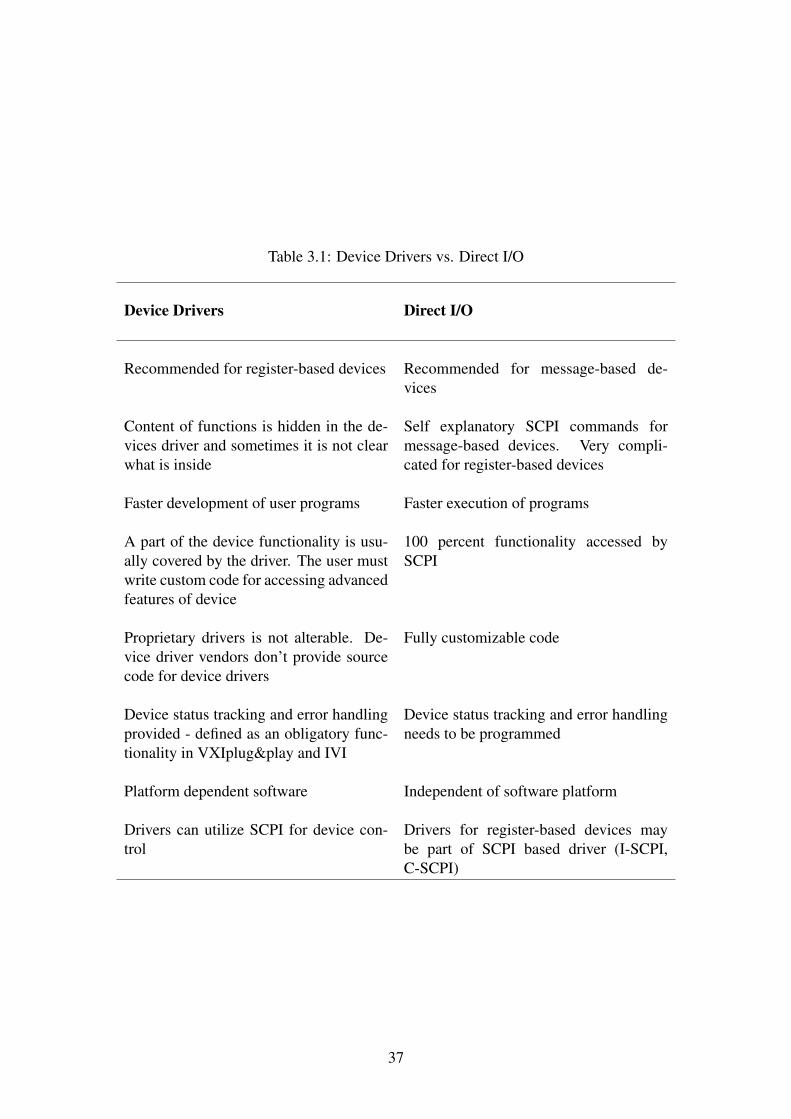
Table 3.1: Device Drivers vs. Direct I/O
Device Drivers Direct I/O
Recommended for register-based devices Recommended for message-based de-vices
Content of functions is hidden in the de-vices driver and sometimes it is not clearwhat is inside
Self explanatory SCPI commands formessage-based devices. Very compli-cated for register-based devices
Faster development of user programs Faster execution of programs
A part of the device functionality is usu-ally covered by the driver. The user mustwrite custom code for accessing advancedfeatures of device
100 percent functionality accessed bySCPI
Proprietary drivers is not alterable. De-vice driver vendors don’t provide sourcecode for device drivers
Fully customizable code
Device status tracking and error handlingprovided - defined as an obligatory func-tionality in VXIplug&play and IVI
Device status tracking and error handlingneeds to be programmed
Platform dependent software Independent of software platform
Drivers can utilize SCPI for device con-trol
Drivers for register-based devices maybe part of SCPI based driver (I-SCPI,C-SCPI)
37

38

4
Thesis
4.1 VXI Measurement and Control System DevelopmentIssues
A typical commercial VXI device is encapsulated in one module with complete backplaneand front panel interfaces. Such device is provided with a dedicated driver, documentation,tutorials, etc. Its integration into VXI system is costly but easy to do. The situation becomesmuch more difficult when the developer of a VXI system must simultaneously integrate a pieceof electronics specific to his needs. Nowadays, there are two major reasons for the difficulty ofthe efficient setup and support of specific VXI systems:
(a) the lack of hardware designers who know all necessary details of standard interfaces,
(b) the cost of time consuming software development.
Reason (a) is addressed to device developers. In order to build a device that may be usedin a VXI system, a huge number of rules from several detailed specifications must be fulfilled.This work overhead, forced by obligatory standards, plays a significant role in the device de-velopment process. In the case of simple electronics, more time is required for development ofthe VXI interface than for development of the functional part. The VXI interface implemen-tation also requires from the device developers precise knowledge of many details of the VXIspecification. This means several weeks spent on studies, which quickly converts into money.
The birth and boom of powerful FPGA chips gave impetus to further evolution of modulardevices for measurement and control. The advanced technology has come to the point wheredevice components are encapsulated in specific integrated circuits which become guarded se-crets of the companies. In some cases this makes the life of device developers easier. Manychips available on the market provide complete functionality for different interfaces such asRS-232, VME, IEEE 488.1 or VXI (register-based devices) [47]. Transformation of user elec-tronics into register-based devices is relatively easy, into message-based devices significantly
39

more complicated. An appropriate interface circuit must provide a much broader functionalitybased on the IEEE 488.2, VXI standards, and SCPI specification.
Reason (b) is addressed to developers and users of VXI systems. Most devices in VXIsystems can be controlled only by software. The integration of a brand-new device into a VXIsystem requires highly sophisticated software, either provided by the manufacturer or devel-oped by the user. The software from manufacturer often doesn’t meet the needs of a specificuser. The user must then rewrite or adapt the device driver for his system or — as is the mostcommon situation — write completely new software from the beginning, which costs an enor-mous amount of time.
4.1.1 Problems with Development of Message-based Devices
Reason (b) is not an issue for the message-based devices programmed by SCPI. Such a de-vice is described by self-explanatory SCPI trees which cover 100% of the device functionality.The user software only needs to send and receive textual messages.
The simplicity of the message-based device programming was achieved by increased com-plexity of its interface — reason (a) becomes an important issue. In this case the developerof a device encounters difficulties during implementation of a VXI interface compliant withIEEE 488.2 and using SCPI messages. Figure 4.1 presents a general block diagram of a VXImessage-based device. For comparison, a typical register-based device contains only a VXIinterface with configuration registers, and a user device. The message-based device compliantwith IEEE 488.2 contains all blocks presented in the figure. The VXI interface contains config-uration and communication registers as well as additional options for IEEE 488.2 compliance.Every block in the figure includes comments on which standard or specification is defined eachfunctional block. As one can see some blocks are a mixture of two standards. While readingthe documentation, dependencies between standards are sometimes not so clear. The specifi-cations define many rules and some of them generate ambiguous interpretations which mustbe solved by the developer. In addition, there are no guidelines or publications which presentpractical ideas of VXI message-based interface implementation.
It is also important to mention that new block Trigger Control appeared in figure 4.1. Thisblock differentiates the message-based from register-based devices. Register-based devices areallowed to use trigger lines available in the VXI backplane in a completely device dependentmanner. In message-based devices the behavior of Trigger Control is defined in the SCPIspecification as a Trigger Model. The Trigger Model determines, in a unique manner, reactionof message-based devices on trigger signals. One can find a more detailed description in [43].
The complexity of the VXI, IEEE 488.2 standards and SCPI specification is very high andthe successful implementation of all of them consumes a lot of time. Realization of such devicesin a small laboratory environment is almost impossible without prefabricated components. Al-though the required standards are in the public domain and are available for developers, the time
40

VXI Interface( VXI Standard Rev. 3 )( with option for IEEE 488.2 devices)
Message Exchange Control
( IEEE 488.2 – 1987 )
Parser, Formatter( Syntax: IEEE 488.2 )
Execution Control( Semantics )(Common Commands by IEEE 488.2)( SCPI by SCPI Specification )
User Device
Trigger Control(Electrical by VXI Std.Logical by SCPI Spec)
VXI Bus
Figure 4.1: Complexity of VXI Message-based Device
required for their implementation is unreasonable. The details of prefabricated, commercialmessage-based tools are guarded by the device manufacturers and their cost is relatively high.The cost of commercial, ready to use message-based devices is usually three times higher thanthat of register-based counterparts with similar functionality.
The solution for developers of VXI message-based devices in a laboratory environmentwould be a tool that offers a complete VXI interface with a configurable SCPI driver. The de-veloper would only need to implement the functionality specific for his electronics.
4.1.2 Existing Commercial Solutions
Up to now, four commercial products have appeared on the market to support development ofthe message-based devices. The one from Interface Technology Inc. (named BB9250) is nolonger available [48] and therefore it is not considered here. Table 4.1 contains a comparisonof the features of the three available solutions.
VXI Technology has released a series of VXI Modular Instrumentation Platform (VMIP)products. There is a single-slot base unit, VM9000, which is a universal C-size breadboardfor mezzanine cards also manufactured by VXI Technology [49]. Among several customizedmezzanine modules, there is one VM7000 card that is a prototyping module for the message-based devices development [50]. Beside several advantages listed in the table, this card hasseveral limitations. It has a fixed and limited list of Common Commands and SCPI com-mands. The command list contains obligatory commands and several SCPI commands for con-figuration of the VM7000 card. Only two commands, :PEEK and :POKE, give access fromthe VM7000 to user device dependent registers. There is no possibility to add specific SCPIcommands; the SCPI parser is able to interpret only pre-defined commands. Using the :PEEK
41

Table 4.1: Comparison of tools for message-based devices development
Feature Racal Instruments7064M
VXI TechnologyVM7000 + VM9000
ICS Electronics5526
Type message-based servant message-based servant message-based servantMessageCapability
Only IEEE 488.2, noextension
Fixed list of IEEE488.2 and SCPIcommands, noextension
Pre-defined IEEE 488.2and SCPI commands,extensions possible
SharedMemory
A24/D16, 64kB no Access from VXI bus tolocal memory
LBUS yes yes noTriggers TTLTRG TTLTRG TTLTRGMaster yes no noInterrupts Programmable
Interrupter, Event andResponse Generator
Static requester onIRQ5
Static requester (IRQline not specified)
UserInterface
Twelve 8-bit TTLbuffers - 96 I/O lines orlocal bus
Only 32 I/O lines,SCSI, power supplylines
32 I/O lines, expan-sion bus (only 64 reg-isters), serial interface,TTLTRG lines
UserCommands
no no yes
and :POKE commands effectively gives operation at register level — the same as for register-based devices. This solution offers a very small number of the features important for the devel-opment of message-based devices.
Racal Instruments has manufactured a message-based prototyping module, series 7064M[51]. This is a C-size PCB with a mezzanine card which serves as a VXI message-basedinterface. The interface card contains a Motorola 68000 CPU for management. The interfaceto the user electronics can be either 96 General Purpose I/O (GPIO) lines or the local busof the 68000. There is a set of C commands for configuration of the interface card and foraccess to the user interface. It implements only a limited and fixed list of IEEE 488.2 CommonCommands. There is no SCPI parser inside and none of SCPI commands is implemented. It isnot possible to add device-specific SCPI commands.
The most advanced tool for the development of message-based devices is produced by ICSElectronics. The product is named VXI-5526 [52]. It is built as a small electronic card witha VXI interface at one side and a user device interface at the other side. It contains a SCPI parserwhich runs on an Intel 386EX processor. The datasheet of this tool mentions that a firmwaredevelopment kit can be used for the definition of specific SCPI commands. Direct contact withthe company resulted in the information that ICS Electronics is not able to sell the developmentkit, but can implement SCPI trees for customers. Effectively, the user has no chance to develop
42
device-specific SCPI commands by himself.
4.1.3 Thesis Motivation
This work is motivated by the lack of appropriate commercially available tools which couldhelp in the development of message-based devices. The solutions presented in the precedingsection don’t offer the capability of defining device-specific SCPI commands, which is cru-cial for user applications. The definition of SCPI trees implies a capability for device drivercustomization, which is also missing. It is also very important that the device developer caniteratively improve his project by changing SCPI command definitions and the device driver inthe laboratory. Ordering a SCPI driver from a company is a very inefficient method for iterativedevelopment.
Besides the limited functionality offered by manufacturers, the price of such tools is alsoa big issue for small laboratories.
4.2 Thesis Statement
Having in mind all these problems and needs, the thesis was formulated as follows:
It is possible in a small laboratory environment to design an effective tool that isflexible enough to integrate some specific electronics into a VXI/SCPI system as a message-based device.
4.2.1 Thesis Goals
The main goal of this thesis is to build an electronic tool which provides a configurable VXIinterface card based on definition of device-specific SCPI commands as well as an editabledevice driver written in a commonly used language.
The tool will be referred to in the further chapters of this work as VXI Message-based Tool(VXI-MBT).
The second goal is to present an example of a VXI-MBT application that demonstrates toolcapabilities and is a practical guide on how to use it.
4.2.2 Requirements for the Thesis Goals
In order to realize the goals, top level requirements for VXI-MBT have been formulated:
1. Flexibility and configurability that allow adaptation of specific user electronics. The fol-lowing derived requirements must be fulfilled:
(a) flexible and configurable user device interface,
43

(b) configurable SCPI trees specific to the user device functionality,
(c) configurable user device driver associated with the defined SCPI trees,
(d) configurable VXI interface.
2. Reduced time for user device development. VXI-MBT should minimize the device devel-oper engagement in the implementation of standard functionality. The developer engage-ment should be focused only on implementation of specific functionality of the adaptedelectronics. The following derived requirements have to be met:
(a) VXI-MBT shall provide the obligatory functionality that is defined by the standardsand shall exist in every message-based device,
(b) a frame for a SCPI processor and a device driver shall be implemented in VXI-MBT,
(c) a user-friendly graphical configuration environment shall be provided — a devel-oper shouldn’t need to learn the format of the configuration files.
3. VXI-MBT should also meet some non-functional requirements in order to ensure usabil-ity over many years. These requirements may help during the development, commission-ing and maintenance of a user devices:
(a) minimize the physical space required for VXI-MBT and maximize space for the userdevice in a VXI module,
(b) upgradeability and maintainability — it shall provide a repository for user projectsthat helps in the long term maintenance of the user device,
(c) since it is assumed that the development of the user device is an iterative processspanning a period of time, an easy upgrade path must be provided.
44

5
Development of User Devices Based on theTool Model
Having in mind all of the obligatory requirements listed in the previous chapter, a generalmodel of VXI-MBT was proposed, as presented in this chapter. The proposed model impliesa development methodology for a user device adapted to VXI standard using VXI-MBT.
5.1 VXI, IEEE 488.2 standards and SCPI in VXI Message-based Devices
This section describes selected features of IEEE 488.2, VXI and SCPI. This information isimportant for understanding the model and implementation of VXI-MBT. This section alsoshows in more details the complexity of VXI message-based devices compatible with IEEE488.2.
5.1.1 VXI Interface for Message-based Devices
Each device in a VXI chassis has a unique address within a 16-bit address space, called the log-ical address. This address, similar to GPIB talker and listener addresses, is 8 bits wide andallows for installation of 256 devices in one VXI system. The addresses on GPIB are 5 bitswide but the basic addressing mode in VXI system is A16. In order to maintain compatibilitybetween GPIB and VXI, the 5-bit GPIB address is converted into a 16-bit VXI address. Bits 15and 14 of VXI address are always ’1’, and the GPIB address is mapped into bits from 13 downto 9. Bits from 8 down to 6 are always ’0’. That’s why, the GPIB address mulplied by 8 givesa logical address on the VXI bus. The remaining bits from 5 down to 1 are used for addressingof VXI configuration and communication registers.
The set of obligatory configuration registers — see appendix D.9 — contains basic param-eters of a device such as type, manufacturer code, device model, addressing modes, addressspace required, interrupt requester and handler lines, etc. When a VXI system is initialized,
45

the controller scans A16/D16 address space looking for installed devices. Based on the con-figuration register contents of each device, the resource manager, which resides in the VXIcontroller, configures memory space for different addressing modes on VXI bus, assigns inter-rupts lines, enables interrupt handlers, etc.
Configuration Register
DeviceSpecific
ProtocolsCommunication Registers
SharedMemoryProtocol
Word Serial Protocol
DeviceSpecific
Protocols
488.2 Syntax
488-VXIbus
DeviceSpecific
Protocols (SCPI)DeviceSpecific
Protocols
Device Dependent Working Register
VXIbus
Figure 5.1: VXIbus Communication Layers
The message-based devices are programmed by sending and receiving textual messages,which must be interpreted and formatted in the device. The stack of communication layersin message-based devices is presented on the far right side of figure 5.1. The message-baseddevices contain, in addition to configuration registers, obligatory communication registers, seeappendix D.9. Communication registers are used to implement various communication proto-cols. Unlike register-based devices where simple reads and writes of registers are performed,in the message-based devices the messages are sent on the VXI bus byte by byte to the samecommunication register, named DataLow. There is a write monitor on the DataLow register,and each message sent through the register is automatically executed by the device. The formatof the messages is determined by the protocol currently applied for the communication.
Word Serial Protocol (WSP) is the only obligatory communication protocol for all message-based devices, see [15] section C.3.3.1. The 16-bit command is sent to a device by writing it tothe DataLow register. The optional response to a command is also placed in DataLow. Read
Ready and Write Ready bits from Response register are used to control the transmission ofwords. VXI defines several commands within WSP. All of them are used for the configurationof advanced functionality of message-based devices, see [15] section E.1. There are also otheroptional communication protocols used for the message transfer.
Commander/Servant Hierarchy. In VME terminology there are two terms, Master andSlave. A master can initiate transmission while a slave can only respond. Each VME devicemust have slave capability but not all need have master capability. This is also true for the com-munication in a VXI system. Here, two additional concepts are incorporated: commander andservant. These two terms, inherent for VXI systems, are used to determine the logical hierarchy
46

among devices. The hierarchy in a VXI system is organized as a reversed tree, and looks likea computer file system. There is one top level commander which usually plays a role of the re-source manager. It is physically located in the slot 0 and can be interpreted as a root of the tree.Several commanders and servants may exist in one VXI system. Servants are always leaves.A non-root commander may exist as a leaf or as a node with other subordinated commanders
and servants. Any VXI device may have only one direct commander, except the top-levelcommander that has no commander above.
The commander/servant hierarchy is particularly meaningful for message-based devicesbecause the communication between them requires WSP protocol. At the beginning, whena VXI system starts, commanders use WSP to configure their direct servants. The Comman-
der/servant hierarchy is useful when reorganization of a VXI system is needed. A part ofthe well configured, existing system with commander/servant hierarchy may be used in a newsystem without reconfiguration.
Interrupts and Asynchronous Events. Most events in the VXI system are asynchronous.When a certain event occurs, another part of the system must be notified. There are severalmethods for notification of event occurrence. The VXI standard takes advantage of the VMEbus interrupt lines. During the initialization process of a VXI system each commander checksthe capabilities of its servants. The commander enables interrupt requesters in the servants andassigns interrupt lines which are monitored by an interrupt handler located in the commander.Commanders which contain an interrupt handler must also have VME master capability in orderto perform an interrupt acknowledge cycle. The commander, notified by interrupt, checks forthe reason of the service request by reading, during the interrupt acknowledge cycle, the statusword from the servant. The interrupt handler routine is completely device dependent and itsbehavior is not defined in the VXI standard.
A servant may also report its status or generate events by sending an appropriate statusword to its commander. This mechanism is called by the VXI standard ’event and signalgeneration’. In such case the servant must have VME master capability. The commander hasa special signal register in the range of the communication registers. When an event occursthe servant writes a 16-bit status word to its commanders signal register. This special wordcontains the sender address and the event code. The commander has a write monitor locatedon the signal register which immediately triggers the event handler. The advantage of eventgeneration is that commanders don’t need to have interrupt handler capability. Servants mayimplement both an interrupt requester and an event generator.
Triggers. The VXI standard extends VME bus by employing outer rows of the P2 con-nector. Ten pins of the additional 64 are used for the trigger lines. Triggering is an essentialmechanism in measurement systems as a hardware method for device synchronization. Inmany applications, measurement devices must be synchronized by fast, non-delayed, globalsignal in order to acquire measurement data at a precise time. Such a possibility is providedby eight TTLTRG and two ECLTRG lines in connector P2. All of them may be used by every
47

device in the VXI system. Minimum assertion time for TTL and ECL triggers is 30ns and8ns respectively. VXI trigger lines are general purpose lines and their usage is device depen-dent. Nevertheless VXI defines three optional protocols such as synchronous, asynchronousand start/stop which may be used for the device synchronization, see [15] section B.6.2.3.
In addition to electrical trigger lines, the VXI standard defines a WSP command for trig-gering devices based on a software synchronization method. The Trigger command in VXIdevices is analogous to the GET command in the IEEE 488 standard. VXI devices which con-form to the IEEE standard should implement the WSP Trigger command. The GET commanddoesn’t guarantee precise synchronization; it is implemented rather for the compatibility withIEEE 488.2.
5.1.2 Conformance of VXI devices to IEEE 488.2 and Message ExchangeControl
Conformance of VXI Device Interface to IEEE 488. The VXI standard also defines how toimplement a VXI device compatible with the IEEE 488.2 standard. The IEEE 488.2 standard issupplementary to IEEE 488.1, but IEEE 488.1 defines a physical interface which doesn’t existin VXI systems. Nevertheless, the VXI standard defines rules which allow controlling VXIdevices as if they were IEEE 488.1 devices. This goal was accomplished by implementation ofspecial commands in WSP, thus, only VXI message-based devices may conform to IEEE 488.1.The VXI standard defines two WSP commands: Byte Available and Byte Request, which areused to exchange the textual messages, the format of which conforms to IEEE 488.2, see figure5.1. An IEEE 488.2 command consists of strings of ASCII characters, which must be sent seri-ally to the device. The Byte Available and Byte Request commands constitute a protocol calledWord Serial Data Transfer Protocol (WSDTP), see [15] section C.3.3.3. The message exchangetraffic is controlled by DIR and DOR bits in the Response register. Other WSP commands suchas Clear, Trigger, Set Lock, Clear Lock, Read STB correspond to IEEE 488.1 control actionssuch as IEEE 488.1 interface management lines IFC, REN, SRQ, and IEEE 488.1 multiple lineinterface command GET and RQS, see [15] chapter D.1.
Unlike IEEE 488.1 the VXI system can have only one listener. The addressing of listenersis also slightly different. The IEEE 488.1 primary address is translated into a VXI base addressmultiplied by 8 as was explained in the previous section. The VXI device should implement ina IEEE 488.2 compatible fashion the IEEE 488.1 functions: SH1, AH1, T6, L4, SR1, DC1 andDT1. The VXI specification precisely describes how these functions have to be implementedin VXI devices, see [15] chapter D.2.
Message Exchange Control is a special finite state machine (FSM) implementing MessageExchange Protocol. Both are defined in the IEEE 488.2 standard. The Message ExchangeProtocol describes how the device has to behave when it receives the messages and preparesthe responses. IEEE 488.2 precisely describes the Message Exchange Control FSM, but there
48

are still some unclear situations which may lead to device malfunctions. Implementation con-siderations concerning such problems are described in [53]. The block diagram of MessageExchange Control and a short description is presented in appendix C.
The IEEE 488.2 standard also defines a set of Status Registers for device status reporting.These registers are described in appendix D.11, figure D.8. Together with the set of CommonCommands the IEEE 488.2 Status Registers provide a unified method for reporting device sta-tus to the control software. The Status Registers must be also implemented in a message-baseddevice compatible with IEEE 488.2.
5.1.3 IEEE 488.2 Syntax and SCPI in VXI Message-based Devices
The SCPI specification defines a set of commands for programming devices in measurementand control systems [16]. SCPI is only a set of commands; it is not a language as it doesn’timplement any conditional instructions. SCPI is an accepted implementation of the IEEE 488.2syntax that goes beyond IEEE 488.2 to address a wide variety of device functions in a standardmanner. SCPI is not dependent on the hardware part of IEEE 488.x. so it may be used with ar-bitrary interfaces such as RS-232, VXI, Ethernet, etc. SCPI provides a consistent programmingenvironment for instrument control and data usage. This software environment consistency isachieved by the use of defined messages, responses, and data formats regardless of manufac-turer [54]. The SCPI specification defines a standard model of a device which covers all func-tional parts of it. The device model is described in appendix B. The use of SCPI significantlydecreases the time for the development of user programs for measurement and control systemsbecause it is independent of programming language and operating system [55].
The SCPI is an open industry standard. Besides the thousands of commands defined inthe SCPI specification, the developer may add custom commands which reflect a specific func-tionality of his device.
The conformance to IEEE 488.2 is the last layer in the communication stack of VXI message-based devices, see again figure 5.1. Each communication protocol which is implemented ontop of IEEE 488.2 is optional with respect to the VXI standard. Nevertheless, SCPI is used asa natural choice for device programming. The IEEE 488.2 standard defines syntax which isa basis for the SCPI specification. Details of SCPI nomenclature based on IEEE 488.2 syntaxis described in appendix B. Each device which uses SCPI must implement thirteen IEEE 488.2Common Commands (appendix D.1) and eleven SCPI commands [17].
The SCPI specification significantly extends the status reporting system defined by IEEE488.2. An additional set of the status registers must be added to the message-based devicescompliant with SCPI. These registers are described in appendix D.11, figure D.9.
49

5.2 The VXI-MBT Model
Taking into consideration the high complexity of VXI message-based devices compatible withthe IEEE 488.2 standard and all requirements defined in section 4.2, a VXI-MBT model wasproposed. The proposed model is presented in figure 5.2. It meets all functional requirementsand inherits the model of VXI message-based devices presented in figure 4.1, with significantextensions important for the thesis. The following paragraphs briefly characterize the featuresof the model.
VXI InterfaceFixed part
Message Exchange
Control
SCPI Processor of IEEE 488.2 Syntax ( Interprets (Interprets
obligatory commands) specific SCPI commands)
Execution ControlVXI-IC Driver Device Driver(Executes obligatory (Executes specific
commands) SCPI commands)
Device Interface(Physical ( Configurable
connector) custom protocol)
Trigger Control(Configurable)
VXI-IC
Commands Definition
TriggerConfiguration
Device Driver Executables
InterfaceConfiguration
VXI Bus
User Device Working Registers or Signals
User Device Functions
Fixed Part Configurable Part
VISA
PC
VXI-SDK-Trigger Control
Configuration- SCPI Trees Definition- Source Code for
Device Driver- Device Interface
Configuration
User Device
SCPI Driver
Figure 5.2: The Model of VXI-MBT
There are three distinct components presented in the figure: VXI-IC, VXI-SDK and a userdevice. VXI-MBT consists of two parts: the VXI-Interface Card (VXI-IC) — the gray box onthe left side, and VXI-Software Development Kit (VXI-SDK) — the gray box on the right side.VXI-IC together with the user device — the black box — constitute a VXI device — a physicalcard cage. VXI-SDK is a software package that resides somewhere in a developer computer.
VXI-IC is a combination of hardware and firmware which provides a VXI message-basedinterface on one side and a user device connector at the other side. Logically, VXI-IC providesfunctionality related to the VXI interface and SCPI driver. VXI-IC is intended to be a ready touse electronic card with embedded firmware that offers to the device developer a flexible VXImessage-based interface.
50
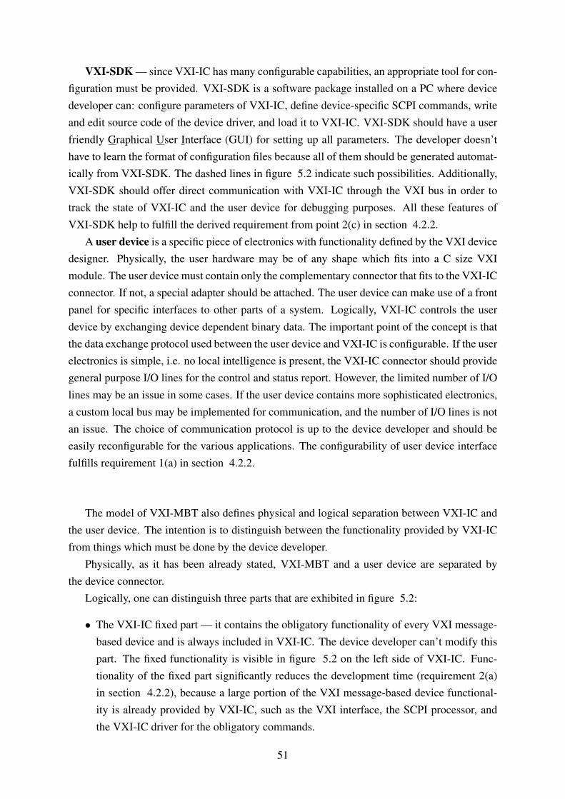
VXI-SDK — since VXI-IC has many configurable capabilities, an appropriate tool for con-figuration must be provided. VXI-SDK is a software package installed on a PC where devicedeveloper can: configure parameters of VXI-IC, define device-specific SCPI commands, writeand edit source code of the device driver, and load it to VXI-IC. VXI-SDK should have a userfriendly Graphical User Interface (GUI) for setting up all parameters. The developer doesn’thave to learn the format of configuration files because all of them should be generated automat-ically from VXI-SDK. The dashed lines in figure 5.2 indicate such possibilities. Additionally,VXI-SDK should offer direct communication with VXI-IC through the VXI bus in order totrack the state of VXI-IC and the user device for debugging purposes. All these features ofVXI-SDK help to fulfill the derived requirement from point 2(c) in section 4.2.2.
A user device is a specific piece of electronics with functionality defined by the VXI devicedesigner. Physically, the user hardware may be of any shape which fits into a C size VXImodule. The user device must contain only the complementary connector that fits to the VXI-ICconnector. If not, a special adapter should be attached. The user device can make use of a frontpanel for specific interfaces to other parts of a system. Logically, VXI-IC controls the userdevice by exchanging device dependent binary data. The important point of the concept is thatthe data exchange protocol used between the user device and VXI-IC is configurable. If the userelectronics is simple, i.e. no local intelligence is present, the VXI-IC connector should providegeneral purpose I/O lines for the control and status report. However, the limited number of I/Olines may be an issue in some cases. If the user device contains more sophisticated electronics,a custom local bus may be implemented for communication, and the number of I/O lines is notan issue. The choice of communication protocol is up to the device developer and should beeasily reconfigurable for the various applications. The configurability of user device interfacefulfills requirement 1(a) in section 4.2.2.
The model of VXI-MBT also defines physical and logical separation between VXI-IC andthe user device. The intention is to distinguish between the functionality provided by VXI-ICfrom things which must be done by the device developer.
Physically, as it has been already stated, VXI-MBT and a user device are separated bythe device connector.
Logically, one can distinguish three parts that are exhibited in figure 5.2:
• The VXI-IC fixed part — it contains the obligatory functionality of every VXI message-based device and is always included in VXI-IC. The device developer can’t modify thispart. The fixed functionality is visible in figure 5.2 on the left side of VXI-IC. Func-tionality of the fixed part significantly reduces the development time (requirement 2(a)in section 4.2.2), because a large portion of the VXI message-based device functional-ity is already provided by VXI-IC, such as the VXI interface, the SCPI processor, andthe VXI-IC driver for the obligatory commands.
51
• The VXI-IC configurable part — this is a hardware and software frame for the imple-mentation of functionality related to the user device (requirement 2(b) in section 4.2.2).The VXI-IC functionality such as trigger control, device-specific SCPI command inter-pretation, device driver and user interface can be configured by the device developerusing VXI-SDK. The configurability of these mechanisms is crucial for the developmentof SCPI drivers for as yet unknown user devices. The configurable elements are locatedon the right side of VXI-IC in figure 5.2.
• user device — as it has been already mentioned, this is a user dependent part. The devel-oper is responsible for its functionality. No functional requirements are specified in thisthesis for the user device.
The components of VXI-IC are briefly characterized here with clear classification of the fixedand configurable features:
The VXI Interface is a part of VXI-IC which is responsible for any interaction with the VXIbus. It must be a message-based servant containing configuration and communication registers.The obligatory WSP protocol must include obligatory WSP commands and optional commandsfor IEEE 488 compliance. It must also include the Byte Request and Byte Available commandsfor WSDTP realization required for the SCPI message exchange protocol. Besides the oblig-atory functions, the VXI interface must support the optional functionality of the VXI bus sothat the user device has the possibility of using it, i.e. interrupt requester, VME master, trig-ger lines, VXI LBUS, 10 MHz clock, and voltages. These features fulfill requirement 1(d) insection 4.2.2.
The SCPI Driver is the local artificial intelligence of message-based devices that performsthree actions:
• Parsing and formatting Common Commands and SCPI commands according to IEEE488.2 syntax. The parser determines if the incoming command conforms to IEEE 488.2syntax; if not it is rejected and an error code is generated. The formatter creates responsemessages by converting returned data from the local processor representation into stan-dardized ASCII strings. The SCPI parser and formatter are fixed. The parser behavior isstrictly defined in the IEEE 488.2 standard and it can parse any SCPI compliant commanddefined by the device developer.
• Interpreting the parsed commands. Even if the SCPI command was parsed successfully,it is not necessarily a command of the particular device. If the command is executableby the device, the interpreter returns its code and parameter list. The parser, formatterand interpreter are enclosed in one component in figure 5.2. The interpreter is par-tially configurable. The fixed part of the interpreter contains a list of obligatory CommonCommands and SCPI commands that are executable by VXI-IC. All other SCPI com-mands are defined by the device developer and definition of them must be generated in
52

VXI-SDK. The configurable part of the interpreter together with the graphical definitionof device-specific SCPI trees fulfill requirement 1(c) in section 4.2.2.
• Executing commands returned from interpreter. The commands are executed by the VXI-ICdriver or by the device driver. The VXI-IC driver executes commands and queries relatedonly to the VXI-IC functionality. The VXI-IC driver doesn’t interact with the user deviceand its presence is not required. The VXI-IC driver executes commands from the fixedlist of the SCPI interpreter. It is an integral part of VXI-IC and cannot be modified bythe device developer. The functionality implemented in the VXI-IC driver is provided toevery user device application. Unlike the VXI-IC driver, the device driver is a fully cus-tomized software object. It is empty by default. The device driver interacts with the userdevice and its behavior is defined by the developer. The configurable device driver fulfillsrequirement 1(b) in section 4.2.2.
5.3 New Development Methodology Aspects of VXI Message-based Devices
The presented model of VXI-MBT implies a new methodology of VXI message-based devicesdevelopment. Figure 5.3 presents an algorithm of the development process which would bethe most general use case of VXI-MBT. The description of the development algorithm includesstatements with the word ’shall’ written in italic. These sentences are simultaneously the spec-ification of VXI-MBT. Every specification statement is followed by a short justification.
At the beginning of the development process it is assumed that the user electronics is readyto be adapted.
In the first step the VXI-IC and user device must be coupled mechanically and electrically.The device interface described in the VXI-MBT model is used for that.
In next step, the developer shall create in VXI-SDK a new project. This project will containall files necessary for VXI-IC configuration created during the development process. Groupingfiles in projects helps with their management. On creating a new project, VXI-SDK shall
automatically generate VXI-IC default configuration files. The developer doesn’t need to createall these files by hand and to learn their format.
Based on the default configuration, the developer shall alter settings of VXI-IC accord-ing to his needs using VXI-SDK. An appropriate GUI in VXI-SDK helps to keep control ofthe VXI-IC configuration — only allowed combinations of configuration options can be chosenby the user. The developer can set configuration options for the VXI interface and/or triggercontrol. The intention of the VXI interface configuration is to make VXI-IC visible in the VXIsystem. The trigger control is configured in order to enable propagation of trigger signals fromthe VXI backplane to the user device and/or to VXI-IC if necessary.
In the next step, the configuration of the device interface shall be performed using VXI-SDK.
53

New Device
VXI-IC
Mechanical & Electrical Coupling
UserDevice
Create new projectin VXI-SDK
InitialProjectFiles
Define new SCPImessages in VXI-SDK
Write Device Driver in VXI-SDK
Configure VXI-IC
Configure DeviceInterface by VXI-SDK
Establish Communicationwith User Device
Load New Configuration tothe VXI-IC from VXI-SDK
Test New Commandsand Associated Functions
VXI Device Works Correctly
Redefine SCPI commands and queries in VXI-SDK
Improve Device Driver in VXI-SDK
VXI Device Ready
No
Yes
Backup Project FilesVXI Device
ConfigurationFiles
Figure 5.3: Development algorithm for new VXI Devices using VXI-MBT
Starting from the possible configuration options of the device interface allowed by VXI-SDK,the developer should be able to assure electrical compatibility between VXI-IC and the userdevice.
When the device interface is configured, it’s time to establish communication betweenVXI-IC and the user device. A method of communication verification shall be provided inVXI-SDK. No additional tools are required for testing the communication with the user device.Therefore, the VXI-SDK software block in figure 5.2 is connected to the VXI bus. VXI-SDKshall communicate with VXI-IC over the VXI bus using the VISA library, as described in sec-tion 3.4, is the most popular mechanism for communication with VXI devices. In addition,this feature enables the possibility of tracking the VXI-IC state at every development stage.
When communication is established, the device-specific SCPI commands can be defined.VXI-SDK shall provide a user friendly, graphical interface for configuration of SCPI trees. Inorder to facilitate the definition process for the developer, the VXI-SDK software can checkthe correctness of new SCPI commands, and forbid violation of the specification. VXI-SDKshall export the SCPI command definition in a format understandable by the SCPI processor
54

in VXI-IC. The format of this file needs only to be understandable by the SCPI processor andthe developer must not change this file.
The complementary process to SCPI message definition is writing the routines of the devicedriver which are associated with individual messages. The VXI-SDK shall provide a text editorin which the developer can write source code for the particular routines. No additional texteditor is required — the routines are automatically assigned to particular SCPI commands byVXI-SDK. The routines shall be written in ANSI C language which is the most commonlanguage for writing device drivers. The VXI-SDK shall use a standard compiler for the devicedriver compilation which is available for free in the Internet. The output file of the compilationis an executable program for VXI-IC processor.
When the definition of SCPI messages is completed and an appropriate device driver hasbeen written, the configuration files generated in the preceding steps must be transferred toVXI-IC. VXI-SDK shall provide a mechanism for file transfer to VXI-IC through the VXI bus.The direct file transfer from VXI-SDK to VXI-IC will speed up the configuration process ofVXI-IC and the overall development process. It also helps to keep control of file versions.
After successful transfer of configuration files to VXI-IC it is time to verify the functionalityof new SCPI commands and the device driver. In this step, the developer can already check howthe driver routines in VXI-IC work with the user device. The VXI-IC shall provide a debuginterface so that debug messages can be printed out by device driver routines. The debuginterface significantly accelerates searching for errors.
At this point the developer can decide whether the developed device works according tohis requirements. If the device doesn’t behave as expected, most probably the definition ofthe SCPI messages or/and the driver routines need to be improved. After necessary modifica-tions, the new configuration files can be loaded to VXI-IC and again tested. These steps aredone in a loop as an interactive process until the SCPI driver operates as it should.
After the iterative process is finished, only one more step should be taken. All project filesgenerated in VXI-SDK during development process shall be saved on the hard drive. It shall
also be possible to save the complete project at any stage of the development process. Thisoption provides the possibility of resuming the development process at any time. It is alsoimportant for future upgradability and maintainability.
5.4 Benefits from VXI-MBT
The presented model of VXI-MBT and the proposed methodology of VXI message-based de-vice development using VXI-MBT provide several practical benefits:
• The separation of VXI-MBT and user device functionality is clearly defined. The modeldetermines which functionality is provided by VXI-MBT and what is specific to the userdevice.
55

• The systematic approach to the model of VXI-IC clearly defines which part is fixed andwhat can be configured.
• The model automatically identifies configurable data which must be generated fromthe VXI-SDK and simultaneously determines the functionality of VXI-SDK.
• Application of the presented methodology should accelerate the development process dueto the short time between SCPI driver modification in VXI-SDK and testing of the driverin VXI-IC.
56

6
VXI-MBT Realization
This chapter describes how the main goal of the thesis was realized based on the VXI-MBTmodel presented in chapter 5. The chapter is split in two main sections. Section 6.1 de-scribes implementation of VXI-IC — both hardware and firmware. Firmware is considered inthis chapter as software implemented in VXI-IC. VXI-SDK, the software part of VXI-MBT,is described in section 6.2. All additional details important for this chapter are included inappendices. An overview of the VXI-MBT implementation has been presented in [56].
6.1 VXI-IC Design and Implementation
6.1.1 Mechanical Issues
The tool is realized as an electronic card that is part of the C size VXI module. It has the P1and P2 connectors for interfacing the VXI bus and a connector for a user device. Figure 6.1presents physical dimensions of VXI-IC. The user device and VXI-IC are connected by the J1connector and optionally by some kind of mechanical handle for board alignment. The area ofthe VXI-IC card was minimized in order to leave as much space as possible for user electronics(the gray area in figure 6.1). The user device must contain a complementary connector oran appropriate adapter for the electrical and mechanical connection.
6.1.2 Hardware
The realization of VXI-IC was preceded by analysis of hardware and software requirements.The following functional requirements determined the selection of hardware components usedfor VXI-IC realization:
• As was presented in chapter 5.2, realization of the SCPI driver requires a processor.
• The processor needs some peripheral devices for proper operation such as non-volatileprogram memory, RAM, local bus, etc.
57

VXI-IC20%
User Electronic Card78 %
J1
P1
P2
430
34088 223
3
Front Panel
Mechanical Handle
Figure 6.1: Dimensions of VXI-IC and a User Device
• A digital circuit is required to provide a VXI message-based interface — at least 160signals must be connected through the P1 an P2 connectors.
• VXI-IC must provide a device connector for the user electronics — this connectorshould have an appropriate number of pins for implementation of a local bus to the userdevice.
In order to fulfill all of the above requirements a modern FPGA chip, Virtex II Pro fromXilinx, was chosen as a main component of VXI-IC [57]. It integrates in a single chip a ma-trix of logic cells, blocks of RAM, hundreds of I/O pins and most important — an embed-ded processor PowerPC [58]. This versatile FPGA chip offers a number of features whichmake it useful in various applications. The following list presents only features important forthe VXI-IC realization:
• Single chip implementation which saves space on the VXI-IC board.
• Flexible configuration — FPGA is a reprogrammable device. This feature is essentialat the prototyping stage. A major part of the VXI-IC intelligence is implemented inthe FPGA chip. All peripheral devices are connected to the FPGA and can be controlledthrough GPIO pins. The advantage of the FPGA is that several iterations of VXI-ICfunctionality development can be performed without hardware redesign.
58

XilinxVirtex II Pro
Buffers
P1
P2 SystemACECompact
FlashSocket
RAMDC/DC Configuration Switches
PWR
DEVICE
J1
Buffers
LED
RS232
Power Lines
TTL & ECL Trigger Lines
RS232
Conv
VXIBus
FrontPanel
UserDevice
JTAG
Figure 6.2: Block Diagram of VXI-IC Hardware
• Almost 400 GPIO pins. This number of pins allows connection of all necessary periph-eral devices and interfaces.
• High speed - implementation of the VXI interface in the FPGA with a high local clockfrequency allows pushing the data transfer rate beyond the maximum throughput ofthe VXI bus in A32/D32 mode.
• The IBM PowerPC is a 32-bit RISC, industry-standard processor. The PowerPC issupported by third-party companies with several operating systems, compilers and soft-ware libraries. All peripheral devices of the PowerPC are synthesized from logic cells.The variety of IP (Intellectual Property) cores offered by Xilinx gives high flexibility forcustomization of the processor system. Buses, memory controllers, interrupt controllers,timers, digital interface controllers, etc. can be included in the project on request. Onlynecessary cores need be built in, hence, utilization of the FPGA logic cells can be re-duced to a minimum. The rest of the logic cells are available for the implementationof custom components such as the VXI or device interfaces. Xilinx also provides busbridges and adapters which allow connection of custom FPGA components to the localbus of the processor. All working registers of the custom components can be accessedfrom the processor software.
Due to all these features of Virtex II Pro, only a few additional hardware components werenecessary to build the complete VXI-IC. A rough block diagram of VXI-IC is presented infigure 6.2.
59

The Virtex II Pro doesn’t provide a non-volatile memory for the FPGA configuration andthe processor program. A Xilinx System ACE chip and a CompactFlash (CF) card [59] werechosen to meet both requirements. Xilinx developed the Advanced Configuration Environment(ACE) System for FPGA configuration. The System ACE chip has a local communication busconnected to the FPGA on one side and interfaced to the CF socket on the other. The SystemACE also has a Joint Test Action Group (JTAG) interface which is connected to the FPGA.The advantages of the System ACE and the CF card used in VXI-IC are:
• The System ACE automatically configures the FPGA after the power is turned on. Allnecessary configuration files are stored on the non-volatile CF card. The System ACEhas a JTAG interface which is connected to the FPGA. It can configure several FPGAchips which are in the JTAG chain. The CF card is capable of storing several FPGAconfiguration files from which the System ACE picks one during the configurationprocess. This feature is very convenient during development of VXI-IC.
• The CF card stores files in a file system. There are two types of possible file systems onthe CF card: FAT12 and FAT16. This means that the most popular operating systemsare able to mount the CF file system and access the files. The PowerPC firmware is alsoable to read and write files on the CF card. The CF card is used to store Virtex II Proconfiguration files and configuration files of the VXI-IC firmware. This feature reducesthe need for physical configuration switches located on the VXI-IC.
• The capacity of modern CF cards is impressive, with up to 8 GB now available. Sincethe FPGA and firmware configuration files occupy only a few megabytes of the CFmemory, the rest of the space is available to the VXI-IC user for custom applications.
Sufficient RAM is necessary for proper operation of the processor. It is possible to synthe-size memory for the PowerPC from blocks of RAM in the FPGA, but only 128kB is availablein this type of Virtex II Pro. Hence, external dynamic RAM memory with 32MB capacity wasadded for proper operation of the processor. Although part of the RAM is used by the VXI-ICdriver running in PowerPC, there is still a lot of memory for the device driver.
There is a set of configuration switches on VXI-IC, all of which are connected directly tothe FPGA. Some of them are used for configuration of the FPGA booting process, and onlyone is required by the VXI standard — the VXI logical address of the board. The details ofthe switch configuration are in appendix D.4.1.
There are several connectors on the VXI-IC which play various roles:
• P1 and P2 are standard DIN 41612 male connectors. Their pinouts are strictly definedby the VXI standard. Almost all signals from the VXI bus are wired to different com-ponents of VXI-IC1. The VXI-IC firmware doesn’t make use of all functionality of
1Only analog SUMBUS from the P2 connector is not connected
60

the VXI bus, but makes it available to the user device and to the device driver. Mostof the P1 and P2 pins are connected through buffers which provide appropriate voltagelevel translation and current source capability.
• The PWR connector offers to the user device all voltages available on the P1 and P2connectors. The VXI standard defines several voltages such as +/-12V, +/-24V, 5V, -2Vand -5.2V. VXI-IC uses only 5V, but all are available to the user device.
• The DEVICE connector is an interface for the user device. It is a DIN 41612 femaleconnector. Part of the pins are pre-defined. The 5V, +/-12V and ground pins are alreadyassigned and reflect the location of the same pins on the P1 connector. The reasonis that some VME cards may be attached to VXI-IC. There are also pins with TTL andECL trigger signals wired from the P2 connector to the DEVICE connector. The mostimportant feature of the DEVICE connector is 64 user pins. These pins are connectedto the FPGA through bi-directional buffers. The direction and enabling of the buffersare controlled from the FPGA firmware. The buffers reduce the likelihood of VXI-ICdestruction due to user device failures or wrong connections. The pinout of the DEVICEconnector is described in appendix D.5.3,
• The LED connector is also connected to the FPGA and allows driving 8 LEDs fromthe processor software. Four of them are defined by the VXI standard and should belocated on the VXI device front panel. The other four are available for the user andaccessible from the device driver. The physical location of the user LEDs is not defined— they may be mounted on the front panel or directly on the connector.
• The RS-232 connector is wired to the PowerPC in the FPGA. It is used as a debug portand is configured as a standard input/output stream for the processor. It is especiallyuseful at the development stage when debug messages can be printed out directly fromthe device driver routines. The RS-232 socket can be mounted on the front panel andconnected with VXI-IC by a cable. The RS-232 terminal offers some debug commandswhich may be used by the developer for checking the VXI-IC state. The command listof the serial port is given in appendix D.1.
The VXI-IC was produced as a 10-layer printed circuit board. Figure 6.3 presents a pic-ture with top view of VXI-IC.
6.1.3 VXI-IC Firmware
The VXI-IC firmware is a mixture of FPGA components and software running in the PowerPC.The FPGA firmware is written in the Very High Speed Integrated Circuits Hardware DescriptionLanguage (VHDL). The PowerPC firmware is written in ANSI C. Figure 6.4 presents a block
61

Figure 6.3: A top view of VXI-IC
diagram of the VXI-IC firmware. All components located in the box labeled PowerPC3 are Croutines. Components outside the PowerPC box are implemented in VHDL.
Due to the firmware complexity it is not possible to present all signals and components inone figure. It should be kept in mind that figure 6.4 presents only a simplified diagram ofthe firmware.
VXI-IC is a VXI message-based servant compliant to IEEE 488.2. The firmware was im-plemented according to the Device Status and Message Exchange Diagram and to the MessageExchange Control Interface defined by the IEEE 488.2 specification, both briefly describedin appendix C. Several practical implementations of the IEEE 488.2 device with a IEEE488.1 interface in measurement devices have proved its efficiency and usability [53]. Thissection presents a unique implementation of IEEE 488.2 using VHDL and ANSI C code inthe PowerPC. There is no available literature describing similar solutions for the VXI bus.
In order not to repeat in this document the text of standards, the following sections onlybriefly describe standard features. The unique, custom features typical for VXI-IC are de-scribed more extensively.
6.1.3.1 VXI Interface
The IEEE 488.2 standard describes the device model with respect to the IEEE 488.1 bus.The VXI standard adapted this model to VXI systems, i.e. a VXI message-based device may becompliant with IEEE 488.2 by implementing some optional features. Figures C.1 and C.2 inappendix C are taken from the IEEE 488.2 specification. The IEEE 488.1 bus was replaced bythe VXI bus and the I/O control block presented in the same figures provides a VXI interfaceinstead of the IEEE 488.1 bus interface. The VXI interface in figures C.1 and C.2 correspondsto the set of light gray boxes in figure 6.4. The dark gray boxes in figure 6.4 correspondto similar IEEE 488.2 boxes in figures C.1 and C.2. The differences between them due to
62

VXIWSP
Execution
InputQueue
OutputQueue
Parser InterruptHandler
Formatter
VXI-ICDriver
DeviceDriver
RAMInterface
RS-232Interface
LEDsInterface
SystemACEInterface
User DeviceArbiter
Interrupt Vector
VME SlaveA24/D16 or A32/D16
DeviceInterface
StatusReporting& Errors Queue
RS-232Driver
VME SlaveA16/D16
VME Requester& Master
VME InterruptRequester
VXI Configuration
&Communication
Registers
VXI LBUSInterface
SysACEDriver
VXI
VXI
VXI
VXI
VXI
FrontPanel
SystemACE RAM
FrontPanel
User Device
PowerPC
FPGA
VXI
VXI TriggersControl
& Sense
VXI
OffsetAddress
LOCAL
BUS
Interrupt LinesVXI InterfaceComponents
LEGEND:
MessageExchange
Control
IEEE 488.2 DeviceComponents
Figure 6.4: Block Diagram of VXI-IC Firmware
implementation issues are described in the following paragraphs.
The box labels of the VXI interface indicate which components are defined by the VMEstandard and which are related to the VXI standard. The detailed implementation of the VMEcomponents in VHDL is described in [60]. The details of the VXI message-based servantimplementation are in [61]. The components of the VXI interface are briefly characterizedhere.
The VME slave component responds to a read or write action initiated by a VME master.This is an obligatory feature both in the VME and VXI standards. There are several commu-nication modes defined by the VME standard that differ in the address and data width. Allof them are optional in the VME standard, but at least one of them must be implemented ina VME slave. Three of these modes are implemented in the VME slave component of VXI-IC.The A16/D16 mode is obligatory in every VXI device. This mode is used by a VXI controllerto get access to the configuration and communication registers in the VXI device. The baseaddress of the VXI device in the A16/D16 mode is determined by the obligatory configurationswitch located on VXI-IC. The value of this 8-bit switch is transformed in the VME slave into
63

an A16 address and compared with the address on the VXI bus. A more precise explanationis given in appendix D.4.1. The other two modes, A24/D16 and A32/D16, are used for directaccess to the user device. The use of these two optional modes is explained in appendix D.13.
The VME master initiates communication on the VME bus. The VME master componentis optional in VXI devices and it is implemented when special VXI features are required. Inthe case of VXI-IC, the VME master is used for the VXI event and signal generation mecha-nism. The VXI-IC notifies its commander of an event occurrence in VXI-IC by writing a statusword to the commander register, as described in section 5.1.1. The VME master component isintegrated with the VME bus requester. Prior to the VME master access, the VME bus must begranted by the VME bus arbiter located in slot 0. The VME bus arbiter is notified by the VMEbus requester that bus control is required by VXI-IC.
The VME master component is connected directly to the local bus of the processor. There isa set of C routines which allows control of the VME master from the device driver. The devicedriver can directly send a VXI event to the VXI-IC commander. The list of possible events andsignals generated by VXI devices is in appendix E.4 of the VXI standard.
The VME master capability can be also used by the device driver to initiate communicationwith any device in the VXI system. For example, VXI-IC may take control of a register-baseddevice located in the same VXI system.
The VME master is capable of communication on the VXI bus in several modes. AppendixD.7 describes details of how to use the VME master component directly from the device driver.
The VME interrupt requester is a mechanism used by the VXI servant to notify its com-mander about an event or service request. This is an alternative to the VXI event and sig-nal generation mechanism described in previous paragraph. VXI-IC has one VME interruptrequester, which is connected to the VME interrupt lines on the VXI backplane. It gener-ates interrupt requests and responses to an interrupt acknowledge cycle initiated by the inter-rupt handler in its commander. The VME interrupt requester is implemented as Release OnAcknowledge (ROAK), as defined in the VME specification. The VME interrupt requestercomponent in VXI-IC is configurable. During system initialization, the resource manager as-signs to the VME interrupt requester the VME interrupt line number using WSP commands.The VME interrupt requester is controlled from the PowerPC software and is visible as a setof registers. The device driver can take over control of the VME interrupt requester and useit to generate an interrupt on the VME bus. The status word returned by the VME interruptrequester during the interrupt acknowledge cycle must also be provided from the device driverroutine and it is the same as in the VXI event and signal generation mechanism. Details of howto use the VME interrupt requester from the device driver are in appendix D.8.
VXI configuration and communication registers are defined by the VXI standard. The con-figuration registers are obligatory for every VXI device. The communication registers are re-quired only for message-based devices. Both are implemented in VXI-IC. Appendix D.9 con-tains a list of implemented registers — the gray boxes on the full list of registers. All registers
64
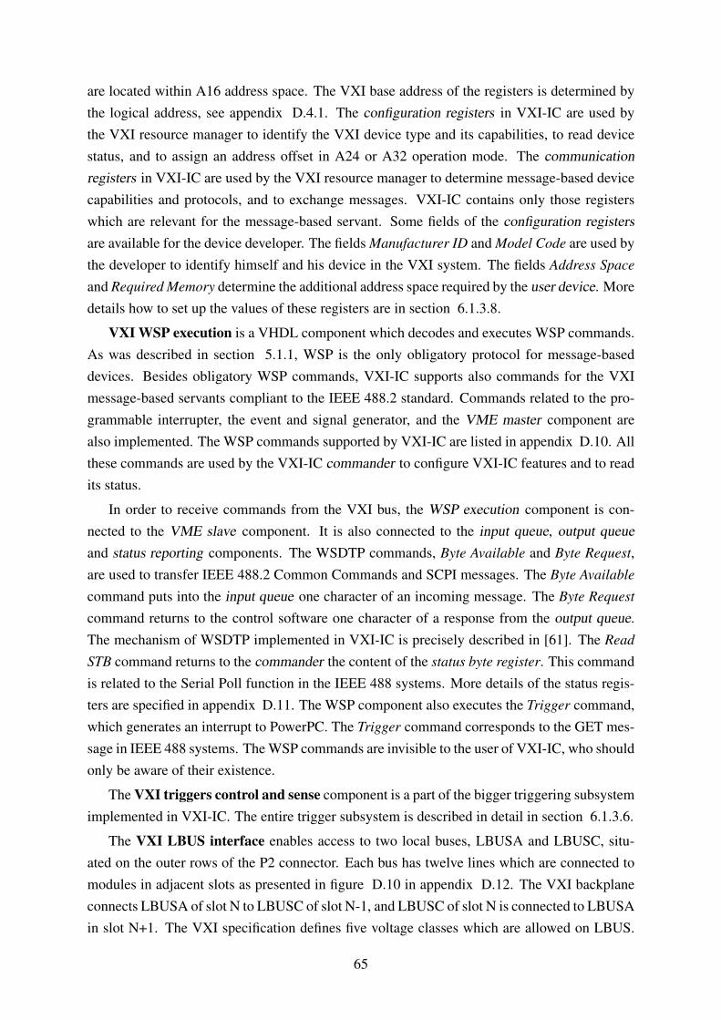
are located within A16 address space. The VXI base address of the registers is determined bythe logical address, see appendix D.4.1. The configuration registers in VXI-IC are used bythe VXI resource manager to identify the VXI device type and its capabilities, to read devicestatus, and to assign an address offset in A24 or A32 operation mode. The communicationregisters in VXI-IC are used by the VXI resource manager to determine message-based devicecapabilities and protocols, and to exchange messages. VXI-IC contains only those registerswhich are relevant for the message-based servant. Some fields of the configuration registersare available for the device developer. The fields Manufacturer ID and Model Code are used bythe developer to identify himself and his device in the VXI system. The fields Address Space
and Required Memory determine the additional address space required by the user device. Moredetails how to set up the values of these registers are in section 6.1.3.8.
VXI WSP execution is a VHDL component which decodes and executes WSP commands.As was described in section 5.1.1, WSP is the only obligatory protocol for message-baseddevices. Besides obligatory WSP commands, VXI-IC supports also commands for the VXImessage-based servants compliant to the IEEE 488.2 standard. Commands related to the pro-grammable interrupter, the event and signal generator, and the VME master component arealso implemented. The WSP commands supported by VXI-IC are listed in appendix D.10. Allthese commands are used by the VXI-IC commander to configure VXI-IC features and to readits status.
In order to receive commands from the VXI bus, the WSP execution component is con-nected to the VME slave component. It is also connected to the input queue, output queueand status reporting components. The WSDTP commands, Byte Available and Byte Request,are used to transfer IEEE 488.2 Common Commands and SCPI messages. The Byte Available
command puts into the input queue one character of an incoming message. The Byte Request
command returns to the control software one character of a response from the output queue.The mechanism of WSDTP implemented in VXI-IC is precisely described in [61]. The Read
STB command returns to the commander the content of the status byte register. This commandis related to the Serial Poll function in the IEEE 488 systems. More details of the status regis-ters are specified in appendix D.11. The WSP component also executes the Trigger command,which generates an interrupt to PowerPC. The Trigger command corresponds to the GET mes-sage in IEEE 488 systems. The WSP commands are invisible to the user of VXI-IC, who shouldonly be aware of their existence.
The VXI triggers control and sense component is a part of the bigger triggering subsystemimplemented in VXI-IC. The entire trigger subsystem is described in detail in section 6.1.3.6.
The VXI LBUS interface enables access to two local buses, LBUSA and LBUSC, situ-ated on the outer rows of the P2 connector. Each bus has twelve lines which are connected tomodules in adjacent slots as presented in figure D.10 in appendix D.12. The VXI backplaneconnects LBUSA of slot N to LBUSC of slot N-1, and LBUSC of slot N is connected to LBUSAin slot N+1. The VXI specification defines five voltage classes which are allowed on LBUS.
65

VXI-IC implements the TTL class on both sides. The utilization of LBUS in VXI-IC is com-pletely user dependent. It is accessible from the device driver. The set of working registers forthe LBUS interface component allows enabling and changing the direction of particular set oflines. The protocol applied on LBUS is not specified. VXI-IC may work as a master or a slave.For the case of slave mode, the firmware in the PowerPC doesn’t know when a transmissionhas been initiated by an adjacent module. In order to notify PowerPC about a transmissioninitiated on LBUS, a dedicated LBUS pin (selected during VXI-IC configuration) generatesan interrupt to the PowerPC. When the interrupt occurs, an empty user entry routine is called.The action taken by this routine depends on code written there by the developer. The interruptdriven LBUS service routine reduces the load on the PowerPC compared to a polling methodfor LBUS event detection. More details on how to use LBUS from the device driver are givenin appendix D.12.
6.1.3.2 Implementation of the IEEE 488.2 Message Exchange Control Interface
The implementation of VXI-IC according to the IEEE 488.2 standard is a crucial point. A shortdescription of the IEEE 488.2 device model is presented in appendix C. The implementation ofthe IEEE 488.2 message exchange protocol (MEP) in the message exchange control interface(MECI) is quite complicated. A similar implementation of the IEEE 488.2 device, but forthe IEEE 488.1 bus, is presented in [53]. It was done using a Motorola 68000 processor andthe TMS9914 integrated circuit from National Instruments. TMS9914 is a single chip withthe IEEE 488.1 interface on one side and Industry Standard Architecture (ISA) bus interfac-ing 68000 on the other side. This chip implements the message exchange control interface.The author of this article [53] proposed modification of the MECI due to the fixed interface ofTMS9914 to the processor.
In case of VXI-IC the IEEE 488.1 interface is replaced by the VXI interface. The imple-mentation of MECI and all other components in VHDL is free of any limitations. All necessarysignals and components which must be connected to the PowerPC are synthesized from FPGAlogic cells. The interrupt vector of the processor has been enhanced, permitting MECI to notifythe PowerPC of events such as incoming messages, reset or WSP trigger commands.
Figure 6.5 presents details of the MECI implementation in VXI-IC. It is a mixture ofVHDL components and C routines. The white components located in the gray box labeledPowerPC are software routines. The components outside the PowerPC are implemented inVHDL. The thin arrows in VHDL mean single signal, and in PowerPC, routine calls. The thickarrows indicate parallel data transfer. Since MECI and MEP are implemented according tothe IEEE 488.2 standard, this section only describes development issues specific to VXI-IC.
Implementation of the parser, execution control, and response formatter is done usingthe C language. The parser and response formatter are relatively easy to implement becausethe specification of the IEEE 488.2 syntax is clear. The execution control is also imple-mented in C, but it is split into two functional blocks: the VXI-IC driver and the device driver.
66

The implementation of the input queue, output queue, and I/O control is done in VHDL. Allof the VHDL components and the software routines are managed by the message exchangecontrol block. It is implemented as a finite state machine with states and transitions defined inthe IEEE 488.2 specification. The functionality of the message exchange control is supportedby the processor interrupts and the set of interrupt handler routines in PowerPC. The state tran-sitions are driven by signals routed from other VHDL components. The PowerPC routines canalso force state transitions by writing to the control register located in the message exchangecontrol.
VXIWSP
Execution
InputQueue
OutputQueue
Parser
InterruptHandler
Formatter
ToolDriver
DeviceDriver
Interrupt Vector
StatusReporting& Errors Queue
MessageExchange
Control
bavbrqdcasgetRMT-sent
OR
ib-emptyib-full
not-ib-emptyreset
input-avail
resp-avail reset
oq-fulloq-empty
clear
clear
reset
reset
DeviceInterface
service-requestsrq
status messages
LOCAL
BUS
pon
get
TriggerControl
trigger
VXI
Device Functions
FPGA
PowerPC
eom, queryp-blocked
ec-blocked
rf-blocked
powerpc-int
Data Byte
Data Byte
Data Byte
Data Byte
prf_reset
OR
Execution Control
Figure 6.5: Block Diagram of the IEEE 488.2 Message Exchange Control Interface Imple-mented in VXI-IC
The MECI has no direct access to the VXI bus. It interacts only with the WSP executioncomponent which is a part of the VXI interface. The WSP execution component handles allVXI related actions relevant for the IEEE 488.2 device. The IEEE 488.2 signals bav, brq,dcas, and get are asserted when the WSP commands Byte Available, Byte Request, Clear, andTrigger, respectively, are executed. There is no WSP command corresponding to the RMT-sent
(Response Message Terminator sent) signal in the IEEE 488.2 specification. The WSP execu-
tion block sets the RMT bit in the response word of the Byte Request command when the lastbyte of the response data is sent to the control software. In parallel to asserting bav and brq sig-nals, the data byte is put into the input queue and taken out of the output queue when the Byte
Available and Byte Request commands, respectively, are executed.
The Status Reporting & Error Queue is connected to the WSP execution by an 8-bit signal
67

named srq. This signal reflects 8 bits of the Status Register Byte, see appendix D.11. This byteis returned to the control software as a response to the Read STB WSP command.
Another important difference from the IEEE 488.2 device is the absence of the device func-
tions block which is present in figure 6.5 of the IEEE 488.2 specification. This part of MECI isuser dependent and it resides in a user device. Nevertheless, the device developer is obligatedto provide standard signal pon which has a dedicated pin in the device connector.
Routing of the signals from parser, device driver, VXI-IC driver and response formatter
to MECI is done through local bus, because these components are implemented as softwareroutines in the processor. The PowerPC has no general purpose I/O pins which might be usedfor this purpose. In order to do the routing, the MECI has been equipped with a local busslave component and an internal control register. This register contains bits which correspondto the signals eom, query, p-blocked, ec-blocked, and rf-blocked from the IEEE 488.2 speci-fication. When one of the signals must be asserted the appropriate software routine sends toMECI the control byte with the corresponding bit set to one. The MECI has a write monitoron the control register and it reacts to the control register writes as if the regular signal wasasserted. The signal routing in the opposite direction, from MECI to the processor, is donethrough the PowerPC interrupts. The parser, driver, trigger control or formatter is launchedby the interrupt handler when an appropriate interrupt is generated by MECI. For example,the parser doesn’t need to check in the loop whether a data byte has appeared in the inputqueue; in this time, the processor does other tasks. When an interrupt occurs, the interrupt han-dler routine checks the reason for the interrupt. If the input-avail signal (interrupt) is assertedthe parser routine is called with parameter not-ib-empty.
The PowerPC has only one external interrupt pin, so an external interrupt vector was im-plemented in VHDL for connection of more interrupt sources. The interrupt vector has manyinterrupt sources but only signals important for the MECI implementation are presented in fig-ure 6.5. The interrupt enabling and priority mechanism, which is not visible in figure 6.5, helpsto avoid improper ordering in the handling of the interrupts. In addition to the input-avail inter-rupt, there are three other interrupt sources. The get interrupt is just a forward of the get signalwhich is asserted by the WSP execution when the WSP Trigger command is executed. Whenthe get interrupt occurs, the trigger control routine is called. More details of the trigger subsys-tem are shown in section 6.1.3.6. The prf-reset interrupt originates from the dcas signal whichis asserted by the WSP execution block when the WSP Clear command is executed. Whenthe prf-reset interrupt occurs the parser, response formatter, device driver, and VXI-IC driver
are reset. The last interrupt, service-request, is asserted by the user device. There is a dedicatedpin in the device connector which is wired to the interrupt vector. This interrupt is used bythe user device to notify the formatter that data for a response is ready. When the service-
request interrupt occurs, the interrupt handler calls the response formatter with the resp-avail
parameter. The service-request interrupt is used when overlapped commands or queries areexecuted. In the overlapped mode the PowerPC performs other tasks while the user device
68

processes messages. The interrupt driven PowerPC software profits by saving processor time,which may be used for other tasks.
The last important extension of the IEEE 488.2 standard is the execution control. In fig-ure C.1, the execution control is presented as one block, which performs actions according tothe parsed SCPI commands and queries. The execution control in the VXI-IC firmware is splitinto two software modules, the device driver and the VXI-IC driver, as presented in figure 6.5.The drivers perform the same tasks as the execution control in IEEE 488.2, but they executetwo disjoint sets of SCPI commands and IEEE 488.2 Common Commands. The predefined setof commands consists of obligatory Common Commands, obligatory SCPI commands, VXI-ICdiagnostic and trigger commands. This set of commands, listed in appendix D.1, is executedby the VXI-IC driver. The VXI-IC driver is not alterable by the device developer and it isalways included in VXI-IC. The device driver executes SCPI commands specific for the userdevice. The set of device-specific SCPI commands is defined during the development processof the user device. Each device-specific SCPI command must have an associated executionroutine in the device driver. The device driver is written during development of the user de-vice and it is compiled every time that a new device-specific SCPI command is defined. Thisdivision into two parts is essential from the development point of view. Even if all routines ofthe device driver are erased, VXI-IC still works because the VXI-IC driver is never affected bythe developer activity.
6.1.3.3 Parser and Formatter
The parser is implemented as a set of C routines and is executed by the PowerPC [62]. Figure6.6 presents the interaction of the parser with other components in VXI-IC.
When the VXI-IC firmware starts, the definitions of Common Commands and SCPI com-mands are loaded from the CF card to the RAM. The list is used by the parser for commandinterpretation. The parser is not active when the input queue is empty. When at least one byteof a new command appears in the input queue, an interrupt is generated to the PowerPC, seefigure 6.5. The interrupt handler then launches the parser routine.
The parser fetches from the input queue data bytes, which are message characters, andstarts the parsing process. Each time before the next character is taken out from the inputqueue, the parser checks that the queue is not empty — signal ib_empty not active. Duringthe parsing process, the parser verifies that the incoming command is syntactically correct. Inthe next step, the parser interprets the command by checking whether it has a related entryin the commands list in the RAM (i.e. whether the syntactically correct command may beexecuted by the particular device). After the input command has been successfully interpreted,the parser puts into RAM output data which is simultaneously input data for the executioncontrol. This data contains: a command code, an optional list of suffixes, if such exist forthe particular command (e.g. :INPut:CHAN3 - where 3 is the suffix; a command may containzero, one, or more suffixes), and a list of parameters, if such are defined for the particular
69

Input Queue
Parser
RAM:1. Command Code2. Suffices Table3. Params Table
ib_empty
eom bit
query
eom
reset error
Error Queue
Data Byte
BinaryData
ErrorCode
RAM:1. Common Commands Def.2. SCPI Commands Def.3. Params Definition
Binary Data
InterruptHandler
MessageExchange
Control
RS/232Interface
debugmessages
not ib-empty
Figure 6.6: Data and Control Flow from/to the VXI-IC Parser
command (a command may have zero, one, or more parameters). If the parsed command wasa query, the query signal is asserted. If the parser detects an eom bit, (a ninth bit of the data bytein the input queue), it also asserts the eom signal connected to the message exchange controlcomponent. In the case of the parser error, the eom signal is not asserted. After the commandhas been successfully parsed, the parser returns to the idle state.
If an exception occurs during the command parsing or interpretation, the parser reportsan error by asserting the error signal and putting an error code to the error queue. The invalidcommand is not executed and the parser returns to the idle state.
The formatter is only a set of C routines which are invoked when new response data isready. The goal of the formatter is to convert response data from local data types into a characterstring and put it into the output queue. The formatter is launched only when a query messagehas been parsed. Otherwise, it is not allowed to put any data to the output queue. If somethingappears in the output queue when MECI is not in the Query state, it should generate a protocolerror. The data and signal flow is presented in figure 6.7.
The developer is provided with the set of formatting routines which format the elementsof response messages according to the IEEE 488.2 syntax. The list of formatting routines isin appendix D.15. The formatter routines take a portion of the response data as a routineparameter, convert it to a character string, and put it into the output queue. When the lastportion of data is formatted, the developer must launch the formatting function with the eom
parameter set to true, see appendix D.15. Then the formatting routine puts into the outputqueue, together with the last character, a data byte which has the ninth bit set to one. It is laterused to set the RTM-sent bit in the response word of the WSP Byte Request command. This
70

Output Queue
Formatter
oq_full
rf_blockedreset
error
Error Queue
Data Byte
ErrorCode
RAM:Response Data
Binary Data
InterruptHandler Message
ExchangeControl
RS/232Interface
debugmessages
RMT-sent
Tool Driver
DeviceDriver
DeviceInterruptRoutine
Figure 6.7: Data and Control Flow from/to Formatter
tells the control software, when reading the response from VXI-IC, that the last character wasreceived.
The data to be sent resides in the RAM. The source of data can be the VXI-IC driver, the de-vice driver, or the the device interrupt routine. For the VXI-IC driver and the device driver,the response generation and formatting are a part of the driver routine. The device developerneeds to invoke in the driver routine appropriate formatting routines which put the responsedata into the output queue. The service request interrupt is generated by the device whenthe query is executed in so-called overlapped mode. The implementation of the sequential andoverlapped modes of command execution is described in appendix D.14. There is a user entryroutine for handling of the service request interrupt. This routine is filled out by the devicedeveloper according to the behavior of his device. The routine is mainly intended to formatresponse data fetched directly from the user device.
If the output queue is full, the formatting routines assert the rf-blocked signal and the for-matting routine waits for room in the output queue. If an error occurs during the responseformatting process, the formatting routine asserts the error signal and puts the error code intothe error queue.
There is also a possibility to print debug messages on the RS-232 Interface of VXI-IC. Thishelpful option may ease the debugging process for the developer.
71
6.1.3.4 Command Execution Mechanism
As was already mentioned, the execution control consists of the VXI-IC driver and the devicedriver. Both are also sets of C routines and they run in the PowerPC. The data and signalsflow of the execution control is presented in figure 6.8. The execution control contains onemain routine which is called when a new message is parsed. This routine reads data from RAMwhich was put there by the parser. First of all the execution control checks the command code.Depending on the type of the command code, the VXI-IC driver or device driver is called.The main routine of the execution control knows which SCPI commands and Common Com-mands are executed by the VXI-IC driver and which by the device driver, and what routinesare associated with these commands.
Execution Control
Tool Functions
Ec-clocked
reset
error
Error Queue
BinaryData
Error CodeMessageExchange
Control
MessageExchange
Control
RAM:1. Command Code2. Suffices Table3. Params Table
Interrupt Handler get
Tool Driver
Device Driver
DeviceFunctions
BinaryData
BinaryData
RAM:1. Response Data
BinaryData
BinaryData
RS/232Interface
debugmessages
Figure 6.8: Function Block Diagram of the Execution Control
The VXI-IC driver is a set of routines associated with pre-implemented commands deliv-ered with VXI-IC. This driver is constant and cannot be changed by the developer. The com-mands executed by the VXI-IC driver are listed in appendix D.1. The VXI-IC driver routinesonly act on the VXI-IC functionality. Presence of the user device is not required for the VXI-ICdriver.
The device driver is empty when a new project is created. It is only meant to collect driverroutines for device-specific SCPI commands and Common Commands which are not executed
72
by the VXI-IC driver. The device driver controls user device functions. But it may interact withthe VXI-IC functions as well, e.g. LBUS communication on the VXI bus. The developer mayalso define SCPI functions which extend the functionality of VXI-IC itself without interactingwith the device driver.
When the VXI-IC driver or the device driver routine execute a query, the response datamust be generated. The form of non-formatted response data is up to the developer, because,as was explained in the previous section, the developer uses the formatter routines to convertthe data into a character string.
When an error occurs during the driver routine execution, the error signal must be assertedand the error code must be put into the error queue. In order to do that, the developer needs tocall a special C routine with the error code as an argument — the rest is done by this routine.
There is a possibility to print debug messages on RS-232 output from the device driverroutines using the standard printf C function. This significantly helps during debuggingprocess of the new routines.
6.1.3.5 User Device Interface
The task of the device interface is to provide an electrical connection between VXI-IC andthe user device. The device interface is physically made up of two connectors. The smaller onemakes available to the user device voltages provided by the VXI backplane, as was described insection 6.1.2. The pinout of the power connector is in figure D.4 in appendix D.5. The largerconnector, marked as DEVICE in figure 6.2, enables communication between VXI-IC softwareand the user device. The user device may be an arbitrary type of electronic equipment. It couldbe a device with a very simple interface consisting of a few control lines and a few status lines,or a complex digital device with a processor and its local bus. With respect to these possibilities,two operation modes of the device interface were proposed.
General purpose I/O mode is useful for simple user devices which don’t implement localbus functionality. In this mode, particular lines or groups of lines may be responsible forthe control and status report functions of the user device. There are 64 GPIO lines which canbe configured by the device developer. The GPIO lines are grouped by eight bits into eightbi-directional buffers. Each buffer can be individually disabled or enabled with appropriatedirection. The device developer needs to configure the GPIO lines in VXI-SDK before the userdevice is connected to VXI-IC. When VXI-IC boots up, the configuration of GPIO lines isautomatically set up and it remains unchanged during operation. The state of each line canbe read and written from the device driver using C functions as well as from control softwareusing SCPI messages, see appendix D.5.3.1. The developer can write device driver routineswhich operate on individual lines or groups of lines connected to the user device.
The device local bus operation mode sets up a local bus for interfacing more advanced userdevices. In this mode, the state of the VXI-IC device connector pins is pre-defined. There are24 address lines, 16 data lines and 5 control lines. The address space of working registers in
73

the user device is mapped into the address space of the PowerPC local bus. Access to the userdevice from the device driver is performed by reads and writes of memory addresses, seeappendix D.5.3.2. The address space reserved for the user device in PowerPC is 16M of 16-bitwords. The data transfer between PowerPC and the user device is controlled by a handshakeprotocol, thus the speed of transmission is adjusted to the speed of the user device. The timingof the handshake protocol is presented in appendix D.5.3.2. The PowerPC is always a masterand the user device is a slave. The timeout mechanism in the PowerPC local bus protects againstsystem failure when the user device doesn’t respond to the read or write operation within 20µs.
There are also several pins in the device connector which have a predefined meaning inboth modes such as power, ground, triggers, device interrupt, etc. These lines are describedin appendix D.5.3. The VXI TTLTRG and ECLTRG trigger lines are wired from the VXIbackplane through low latency buffers directly to the device connector.
6.1.3.6 Trigger Subsystem
The VXI-IC connects eight TTLTRG lines and two ECLTRG lines available on the P2 connec-tor of the VXI backplane. These lines are routed through bi-directional buffers to the FPGA onVXI-IC and simultaneously to the user device, see fig. 6.9.
VXI User
Device
VXI-IC
TTLTRG7..0
ECLTRG1..0
Interrupt Vector
PowerPC
TRG Drivers
Trigger Acceptor
Trigger Source
Figure 6.9: Implementation of triggers in VXI-IC
The direct routing from the VXI backplane to the user device minimizes the propagationtime of trigger signals. The VHDL components of the FPGA operate synchronously with a lo-cal clock at frequency 100MHz (10ns period). The specification defines a minimum TTLTRGpulse length greater than 30ns, hence the trigger control VHDL component is able to detecteach TTLTRG pulse. For detection of ECLTRG pulses the VHDL component works at doubleclock rate. The component latches ECLTRG lines on rising and falling edge of the clock whichgives 5ns sampling time. That fulfills the VXI specification by which the trigger acceptor mustdetect signals with a setup time of at most 8ns, see section B.6.2.3 and B.6.2.4 in the VXI
74

specification.Each TTLTRG and ECLTRG line can be individually set up as an input, output or both.
The VXI-IC can work both as an acceptor and as a source of trigger signals at the same time.Both modes are described below.
The trigger acceptor is implemented as a simple ARM-TRIGger model according to the SCPIspecification [16]. The ARM-TRIGger model assumes four states of the trigger subsystem plusthe device action. The list below presents the SCPI commands which are implemented inthe VXI-IC.
:ABORT:ARM
[:SEQuence[1..8]][:IMMediate]:INITiate
:INITiate[:IMMediate]
:TRIGger[:SEQuence[1..8]]
[:IMMediate]:INITiate:SOURce?:SOURce TTLTrg[0..7]|ECLTrg[0..1]|INTernal
These are all standard SCPI commands described in the specification. Up to eight parallelsequences can be used by the device driver. Only one layer of the ARM state is implemented.The behavior of the trigger subsystem conforms to the state diagram described in the SCPIspecification.
Based on the ARM-TRIGger model, the developer can extend the trigger subsystem func-tionality in VXI-IC by adding new commands defined by the SCPI specification.
All trigger lines are connected to the interrupt vector of the processor. The special entryroutine is invoked by the interrupt handler in the PowerPC when a special event occurs on anyof the trigger lines. Appendix D.18 describes the working registers of the trigger subsystemwhich can be used to detect the source of a trigger.
The trigger source in VXI-IC can drive any of the trigger signals. Each of the TTL or ECLtrigger lines can be driven from the PowerPC software. The SCPI tree was implemented forthis purpose, as listed below:
:OUTput:ECLTrg[0..1]
[:IMMediate]:LEVel?:LEVel <Boolean>
75

[:IMMediate]:STATe?:STATe <Boolean>
:TTLTrg[0..7][:IMMediate]:LEVel?:LEVel <Boolean>
[:IMMediate]:STATe?:STATe <Boolean>
An internal trigger can be generated using the :IMMediate or :LEVel commands.The :IMMediate command causes generation of a trigger pulse by VXI-IC. The :LEVelcommand is used to change a voltage level on the trigger line driver by VXI-IC.
The trigger generated by VXI-IC automatically propagates through the bi-directional buffersto the user device, which allows triggering of the user device directly from VXI-IC.
6.1.3.7 Other Processor Peripheral Devices
Besides several firmware components implemented due to the specification requirements, thereare several VHDL components which are important for operability of the processor. Short de-scriptions of these components are included below to give an overview of additional capabilitiesof VXI-IC. All the described components are presented in figure 6.4.
The RAM interface translates the external memory chip dependent signals into the localbus communication protocol. VXI-IC contains 32MB of dynamic RAM. The memory is orga-nized as 4M of 32-bit words. The entire memory is available for the PowerPC firmware. Part ofthe memory is already used by the parser and it is allocated statically. The rest of the memory isused dynamically by the VXI-IC driver and the device drivers. Standard C memory allocationfunctions such as malloc and free are available for the device driver to use the memory incustom routines.
The System ACE interface component is a bridge between the specific communication busof the System ACE chip on one side and processor local bus on the other. The System ACEVHDL interface is coupled with the System ACE driver of the processor firmware. The Sys-tem ACE driver exports to the PowerPC firmware high level functions for files manipulation.The files stored on the Compact Flash card are used to configure VXI-IC and its firmware. Butthis file system can be also used from the device driver by calling functions from stdio Clibrary such as fopen, fread, fwrite, fclose, etc. The device developer can store onthe CF card any files he wants.
The RS-232 interface together with the accompanying RS-232 firmware driver is a stan-dard input/output feature of the processor firmware. It plays a significant role during debuggingof the device driver. It may be used to display debug messages written from the device driverroutines by the standard printf C function. This is a great help for tracking the execution
76

process of the device driver. The RS-232 also offers a command line interface which allowsexecution of a few single character commands which may be used to check: the list of loadedCommon Commands, SCPI trees, defined errors, etc., see appendix D.6.
The LEDs interface is a component which enables access to the user LEDs from the devicedriver routines. The state of these four LEDs is controlled by a simple 4-bit register accessiblefrom the device driver routines, see appendix D.5.
6.1.3.8 Configuration of VXI-IC
The VXI-IC has several configurable capabilities. All of the configuration options are left tothe device developers. The flexibility of VXI-IC, as was stated in chapter 4, comes from the ex-tensive configuration capabilities of VXI-IC. The configuration of VXI-IC must be stored ina non-volatile manner. There are two mechanisms for configuration storage: switches and files.Most of configuration options are stored in configuration files located on the CF card. As wasdescribed in section 6.1.2, the VXI-IC contains the System ACE chip and the socket for CFcards. One of the CF card tasks is to store these configuration files. Only one feature is con-figured by the switches located on VXI-IC — the logical address of the VXI-IC configurationregisters on the VXI bus. This address switch is required by the VXI specification. The detailshow to set up the logical address are in appendix D.4.1.
The FPGA configuration, binaries of the embedded firmware, commands definition, etc.are stored in the configuration files. The following points briefly describe the role of eachconfiguration file.
The file tool.ace is a binary file that contains the configuration for the FPGA. Thisfile also contains bootloader software for the PowerPC. The VXI-IC has no EPROM for storingconfiguration; the System ACE with CF card is the only way to configure the FPGA. The FPGAconfiguration is loaded when the VXI-IC is powered on, as described in other chapters. The fileis generated once and delivered with VXI-IC. There is no way for the developer to changethe FPGA configuration. This file is the same for all user device implementations.
The file tool.src contains executables of PowerPC embedded software in HEX format. Thisfile contains all the PowerPC software including device driver, VXI-IC driver and pre-compiledlibraries for the PowerPC operation. This file is generated every time that the device developerchanges the device driver routines.
The file tool.cfg is a text file and keeps several relevant configuration options of VXI-IC.It contains VXI configuration register options such as Manufacturer ID, Model Code, Address
Space, and Required Memory. In addition, this file also includes configuration of the deviceinterface and many other options. The tool.cfg file is generated automatically from VXI-SDK.A dedicated graphical panel in VXI-SDK maintains this configuration file, as described inother chapters. This file is generated by the device developer every time that the configurationof VXI-IC is changed. All details of the configuration options in tool.cfg are described inappendix D.4.2.
77

The file *.scp has an arbitrary name which is defined in tool.cfg. This text file isused to store definitions of Common Commands and SCPI commands which are interpretedby the parser. It contains definitions of both VXI-IC commands and device-specific SCPIcommands. The file is loaded to PowerPC memory during the boot up process and remainsthere until power is turned off. The *.scp file is an input for the SCPI parser in VXI-IC.This file is also generated from VXI-SDK when SCPI commands definitions are altered bythe device developer. Section 6.2.4 describes how to generate the *.scp file.
The file error.txt keeps in text format a list of possible error numbers and messageswhich may be returned by the VXI-IC firmware according to the SCPI specification. The fileis generated from VXI-SDK when the device developer adds a new error code and messagewhich may be returned by one of his device driver routines. The error configuration procedureis described in section 6.2.3.
All described files are mandatory and must be present on the CF card when the VXI-ICboots up. There are two methods of loading these files onto the CF card. One is to simplyremove the CF card from the socket and plug it into a typical CF reader connected to a PCvia a USB port. The CF card is visible in the OS as a removable storage device. All gener-ated files can then be simply copied from a local hard drive to the CF card. This method isinconvenient when the configuration files are updated frequently. Every time the files must beuploaded, the user device must be removed from the VXI chassis, and the CF card removedfrom the socket and plugged into the CF reader. In order to eliminate this inconvenience, a SCPIcommand in the DIAGnostic tree was proposed. The command :DIAG:FLASh:UPLoad<string>, <ABPD> is used to upload an arbitrary file to the CF card. The first parame-ter of this command is the destination file name and the second parameter is a block of datafrom the file. Using this command, all necessary configuration files can be quickly uploadeddirectly from VXI-SDK. After the files have been uploaded, VXI-IC must be rebooted in orderto read new configuration data from the files. VXI-IC can also be restarted by a SCPI command:DIAGnostic:BOOT sent from VXI-SDK.
6.1.3.9 VXI-IC Initialization Process
The initialization process of VXI-IC is quite complicated due to the enhanced configurability.First of all, VXI-IC must follow rules of message-based device initialization defined by the VXIstandard. In addition, the configurability of the parser, device driver and device interface intro-duces more steps to the initialization process.
According to the VXI specification there are two methods of VXI device status reporting.First of all, there are two bits in the obligatory status register of the configuration registers.These two bits are called Ready and Passed. They are read by the VXI controller to checkwhether the device is ready for normal operation.
In parallel to the status register bits, there are three LEDs on a faceplate of the devicefor visual indication of the device status. Two LEDs reflect the status of the Ready bit and
78
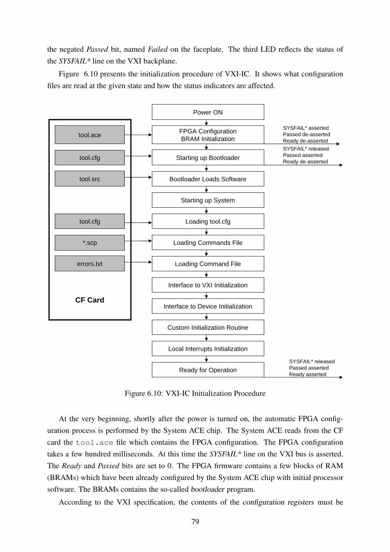
the negated Passed bit, named Failed on the faceplate. The third LED reflects the status ofthe SYSFAIL* line on the VXI backplane.
Figure 6.10 presents the initialization procedure of VXI-IC. It shows what configurationfiles are read at the given state and how the status indicators are affected.
Power ON
FPGA ConfigurationBRAM Initialization
Starting up Bootloader
Bootloader Loads Software
Starting up System
Loading tool.cfg
Loading Commands File
Custom Initialization Routine
Interface to VXI Initialization
Interface to Device Initialization
Ready for Operation
CF Card
tool.ace
tool.src
tool.cfg
*.scp
tool.cfg
Loading Command Fileerrors.txt
SYSFAIL* assertedPassed de-assertedReady de-asserted
SYSFAIL* releasedPassed assertedReady de-asserted
SYSFAIL* releasedPassed assertedReady asserted
Local Interrupts Initialization
Figure 6.10: VXI-IC Initialization Procedure
At the very beginning, shortly after the power is turned on, the automatic FPGA config-uration process is performed by the System ACE chip. The System ACE reads from the CFcard the tool.ace file which contains the FPGA configuration. The FPGA configurationtakes a few hundred milliseconds. At this time the SYSFAIL* line on the VXI bus is asserted.The Ready and Passed bits are set to 0. The FPGA firmware contains a few blocks of RAM(BRAMs) which have been already configured by the System ACE chip with initial processorsoftware. The BRAMs contains the so-called bootloader program.
According to the VXI specification, the contents of the configuration registers must be
79

initialized within 4.9 s.2 As described in appendix D.4.2, some fields of the configurationregisters are defined by the developer in the tool.cfg file. The bootloader reads parametervalues from the tool.cfg file and writes them to the configuration registers before 4.9 spasses. After the register fields are initialized, the SYSFAIL* line is de-asserted and the Passed
bit is set to 1, see section C.2.1.2 in [15]. From this moment all of the configuration andcommunication registers of VXI-IC are accessible on the VXI bus.
The FPGA configuration and bootloader are always the same for each project; the developeris not able to change them. Hence, the bootloader program is used to load PowerPC firmwarecompiled by the developer in VXI-SDK. The PowerPC firmware is loaded from the tool.srcfile to SDRAM. When the PowerPC firmware is loaded, the bootloader jumps to the first in-struction of the firmware. This means that the bootloader is no longer being executed bythe processor; at this moment the main program is running in the PowerPC.
The main PowerPC program also has to perform several initialization steps before VXI-ICis ready to operate. The main program again reads the tool.cfg file from the CF card anduses the configuration parameters for further initialization of VXI-IC and the user device. Formeanings of the parameters in tool.cfg see appendix D.4.2.
In the next two steps, the program reads command and error definitions into SDRAM,which are later used by the parser and the drivers. Next, several registers of the VXI Interfaceare initialized, which prepares the VXI-IC for message exchange.
The device interface, which has been disabled until now, is initialized in the next step. Atthis stage, based on the tool.cfg content, the device interface is configured to the appropri-ate operation mode.
Since initialization of the user device will vary for different applications a custom initializa-tion procedure was added at this point. This procedure is empty by default, but it can be filledout by the developer in VXI-SDK. This procedure can contain any initialization procedure forthe user device, e.g. it can detect the presence of the user device. If the user device initializationfails the overall initialization process is also terminated.
If the user device initialization process succeeds the PowerPC interrupts are configured andenabled. From this moment VXI-IC is ready for normal operation. The Ready bit is set to ’1’only when the VXI controller sends the Begin Normal Operation command.
6.2 VXI-SDK Implementation
The main goal of VXI-SDK is to provide a user friendly graphical interface for the VXI-ICconfiguration. VXI-SDK is written in a high level programming language, MS Visual Ba-sic 6, in the MS Visual Studio 6 software environment. VXI-SDK works on any PC withMS Windows. The installation package of VXI-SDK is on a CD-ROM attached to VXI-IC.
2If the device initialization fails, the SYSFAIL* line remains asserted and the VXI system initialization isstopped.
80

VXI-SDK requires a cross-compiler called powerpc-eabi-gcc which must be installed in addi-tion to VXI-SDK on the same computer. It is a free compiler on a GNU license, downloadablefrom the www.gcc.gnu.org website. A path to the powerpc-eabi-gcc file must be set upin the configuration of VXI-SDK. Figure 6.11 presents the concept of the VXI-SDK environ-ment.
ProjectFiles
tool.cfg
VXI-IC
VXICF CardsReader
in/outthe CF card
VXI-ICConfiguration
SCPI TreesDefinition
*.scp
Editor of Source Code of
Device Driver
PowerPCLibraries
gcctool.src
tool.ace
files
software
hardware
Legend:
VXI-SDK
User ErrorsDefinition
errors.txt
PC
Figure 6.11: The Concept of VXI-SDK
The VXI-SDK environment offers a graphical interface for the following tasks: SCPI treesdefinition, writing source code for the device driver routines, editing of the user entry routines,definition of user errors, and finally, configuration of the VXI interface and the device interface.All these tasks are described in more detail in the next sections.
When the developer starts a new project in VXI-SDK, he gets a basic SCPI tree with com-mands which are already implemented in VXI-IC. The set of all necessary VXI-IC configura-tion files is generated automatically with default initial settings. At every stage of the projectdevelopment, the data can be saved in project files which are stored in a folder selected bythe developer. This allows resuming the project development at any time.
When all tasks within the given project have been performed by the device developer,VXI-SDK generates all configuration files. There are four files generated by the VXI-SDK:tool.src, errors.txt, tool.cfg, and *.scp (command definition). The FPGA con-figuration file tool.ace is not generated in VXI-SDK — this file is provided with VXI-IC.The errors.txt, tool.cfg and *.scp are text files in a format understandable forthe VXI-IC firmware. The developer doesn’t need to understand the format of these files.The tool.src file is in a binary format. It is an output of the PowerPC firmware compilation
81

by the powerpc-eabi-gcc compiler. The compilation process automatically runs in a separatecommand window in which compilation messages are printed out. In the first step of com-pilation, all source code written by the developer is compiled. In the next step, the PowerPClibraries are linked. These libraries contain the main program of PowerPC including the VXI-ICdriver. They are not editable by the developer. Finally, the tool.src file is generated.
All these four configuration files are then ready to be uploaded to CF the card of VXI-IC.The uploading process is described in section 6.1.3.8.
The following sections present short descriptions of operational use cases of VXI-SDK.The screen shots of the VXI-SDK windows give an impression of how to use the environment.
6.2.1 SCPI Tree Definition
Figure 6.12 presents the main window of VXI-SDK. It is split into two panels. The left onecontains SCPI trees, and the right one a complete list of the Common Commands defined bythe IEEE 488.2 standard. The menu of VXI-SDK, which includes all actions, is available onlyin this window. The status bar at the bottom contains a message output for the last error whichoccurred in the program.
On both panels the commands in blue are pre-defined commands implemented in the VXI-ICand executed by the VXI-IC driver, see 6.1.3.4. The blue commands cannot be modified andthe corresponding driver routines are not editable.
Common Commands definition. The list of Common Commands is fixed. All of the com-mands with their parameters which are defined by the IEEE 488.2 standard are already inthe list. There are 41 commands but only 13 are implemented in VXI-IC. These 13 commandsare defined as obligatory in the IEEE 488.2 specification. They are executed by the VXI-ICdriver. The rest are the optional commands. In order to implement one of the optional com-mands the developer needs only to check the corresponding box in column ID (right side offigure 6.12). In order to remove one of the Common Commands from the project, it mustbe only unchecked. It is not possible to uncheck an obligatory Common Command. The texteditor with the corresponding device driver routine is available under the context menu of eachcommand, see section 6.2.2.
SCPI trees definition. The elements in black in the SCPI trees are commands defined bythe developer. The definition of a new SCPI command is performed by building the tree nodeby node. All editing options for the SCPI trees are available in the context menu. Addinga new node/leaf is performed by clicking the right mouse button on the preceding tree elementand choosing an appropriate action such as: add next, add child, change or remove. Thesefour options cover all editing possibilities for the SCPI structure. The VXI-SDK takes care ofthe syntactical coherence of the SCPI trees. For example, the node can’t be left without a leaf,because only nodes with leaves at the end form the complete commands.
The definition of each element of the SCPI tree is done in a separate window where all
82

Figure 6.12: Main window of VXI-SDK
information must be provided by the developer. Figure 6.13 presents the window with param-eters of the SCPI command element.
The presented window permits the definition of both a node and a leaf of the SCPI com-mand. On the left side of the window, several options of the command element can be deter-mined. On the right side is a panel where command parameters can be defined. The parameterspanel appears only when the Parameters checkbox on the left side is marked. Depending onthe parameter type chosen on the right side different configuration options appear below, whichcharacterize specific features of the parameter. When the command element is fully definedthe developer needs to save it. The command definition window then disappears and the de-fined element is shown in the SCPI tree structure. All details concerning SCPI commands anddefinition of parameters are in appendix D.16.
The SCPI trees defined in VXI-SDK are automatically checked according to the IEEE 488.2syntax. But the final proof of syntax correctness comes from the parser in VXI-IC.
83

Figure 6.13: SCPI command and parameters definition
6.2.2 Writing a Device Driver
The main advantage of VXI-MBT is that the developer can write a device driver which iscomplementary to the device-specific SCPI commands. Each device-specific SCPI commandis associated with one device driver routine. The routine declaration is generated automaticallywhen the new SCPI command is defined. There is an option edit driver in the context menu ofthe SCPI command. This option opens the editor window presented in figure 6.14.
The declaration of the device driver routine includes the routine name and its arguments.The first argument is a pointer to a list of the optional parameters of the parsed command,the second argument is a pointer to a list of the optional suffixes which were found in the parsedcommand. The body of the routine is empty by default and is filled out by the developer.The source code of the device driver routines is written in C.
Several built-in C routines are implemented in the VXI-IC firmware. These routines can beused by the developer to get access to various functionality of VXI-IC such as device interface,interrupt requester, VME master component, error queue, etc. All these functions are listed inappendix D.17 and explained in different sections of the dissertation.
When all routines have been written, the developer needs to compile the device driver.The compilation command is available in the Project menu. The VXI-SDK gathers all the de-vice driver routines, creates a make file, and executes it in a separate command window. The re-sult of the compilation is printed in the command window, so that the developer can read mes-sages generated by the compiler. After successful compilation, the binary file is ready to beuploaded to VXI-IC.
User entry routines. There are also several so-called user entry routines which are builtinto the VXI-IC firmware. Unlike the device driver routines associated with device-specificSCPI commands, the user entry routines are called by the VXI-IC firmware when a certainevent occurs. They are empty by default. The goal of these routines is to give the developer
84

Figure 6.14: Edition Window for a Device Driver Routine
the possibility to write custom C code to react properly to special events. The content of theseroutines is developer dependent. The following user entry routines are available for the devel-oper:
• Service request interrupt handler — this routine is called when the user device generatesan interrupt. This routine is useful for the formatter when a response data is returnedby a command which is executed in an overlapped mode. The command execution inthe overlapped mode is described in section 6.1.3.3.
• Trigger interrupt handler — the routine is called when a trigger is detected by the VXI-IC.The source of the trigger can be: TTLTRG lines, ECLTRG lines, or a WSP Trigger com-mand. The developer can precisely determine the trigger source by reading the appropri-ate working register of VXI-IC. The triggers handling procedure is described in appendixD.18.
• Device initialization routine — this routine is called when the VXI-IC is in the initializa-tion process. The user device may need to be initialized when the VXI-IC is initialized.Using this routine the developer can write his code for the user device initialization.The precise point of calling the routine in the VXI-IC initialization process is describedin section 6.1.3.9.
85

• LBUSx interrupt handler — this routines is called when a signal level transition is de-tected on a selected line of the LBUSA or LBUSB on the VXI chassis backplane. The rou-tine allows a proper reaction of VXI-IC on an action initiated by an adjacent VXI module.The details of the LBUSx programming are in appendix D.12.
• Common Commands user routines — there are three Common Commands, *CLS, *RST,and *TST?, of the 13 implemented in VXI-IC which have user entry routines associatedwith them. These commands also contain associated VXI-IC driver routines which per-form actions related to the VXI-IC functionality. Nevertheless, the developer may wantto add to these commands some actions related to his device. In this case he can write hissource code in these user routines. More details are in appendix D.1.
6.2.3 User Errors Mechanism
VXI-IC contains the obligatory status reporting structure defined by the IEEE 488.2 standardand SCPI specification. Both structures are presented in appendix D.11. The SCPI compliantstructure includes the questionable status register, the operation status register, and the er-ror/event queue. The last is used for reporting any error or event in the VXI/SCPI device.The code of an event/error is put in the error/event queue when an exception takes place inthe VXI-IC. The parser, formatter, or VXI-IC driver can generate an event/error. The devicedriver is also able to insert an event/error code. The device developer needs to use a C functionnamed
int addErrorToQueue(int errNumber)
with the event/error code passed as a parameter.
The control software can read the event/error codes and corresponding messages using a setof obligatory SCPI commands. Each VXI/SCPI device must implement the following SCPIcommands from the :SYSTem:ERRor subsystem:
:SYSTem:ERRor
:ALL?:CODE
:ALL?[:NEXT]?
:COUNt?[:NEXT]?
This subsystem consists of SCPI commands and queries used for control of the error/eventqueue. When the control software sends the query :SYSTem:ERRor:NEXT?, VXI-IC sendsback a response which consists of the numeric value of the error followed by a comma and
86

the quoted error message. When no error has occurred, the zero value is returned and the re-sponse looks like 0, "No error". When an error is reported, the non-zero value andthe matching message is returned e.g. -100, “Command error”. The meanings of otherSCPI commands and queries are precisely defined in the SCPI specification in chapter 21.8.
The error/event code is an integer number in the range from -32768 to 32767. All negativenumbers are reserved for the SCPI standard but until now only a few tens of them are used. Allerrors defined in the SCPI specification are included in VXI-IC. The range of positive errornumbers is reserved for developers. A few of the positive numbers have been already usedfor custom functionality of VXI-IC. The rest are left for the device developer. The developercan define a custom error and an associated message. Figure 6.15 presents the VXI-SDKwindow in which the errors/events and their messages are defined. Blue entries are the non-
Figure 6.15: User Errors Definition Window in VXI-SDK
editable errors defined by the SCPI specification. All other errors can be modified and removed,or new ones can be defined in this window. When the list is complete, VXI-SDK generatesthe error.txt file and uploads it to VXI-IC. When VXI-IC boots up, it loads all errors fromthe file into a static array in the program memory. This file is automatically added by VXI-SDKto every new project with all pre-defined SCPI and VXI-IC errors. The device developer canuse the newly defined error/event codes in the device driver for his specific needs.
87
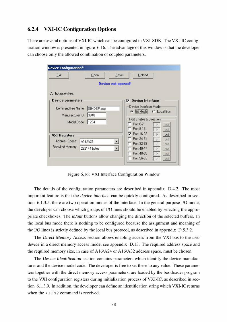
6.2.4 VXI-IC Configuration Options
There are several options of VXI-IC which can be configured in VXI-SDK. The VXI-IC config-uration window is presented in figure 6.16. The advantage of this window is that the developercan choose only the allowed combination of coupled parameters.
Figure 6.16: VXI Interface Configuration Window
The details of the configuration parameters are described in appendix D.4.2. The mostimportant feature is that the device interface can be quickly configured. As described in sec-tion 6.1.3.5, there are two operation modes of the interface. In the general purpose I/O mode,the developer can choose which groups of I/O lines should be enabled by selecting the appro-priate checkboxes. The in/out buttons allow changing the direction of the selected buffers. Inthe local bus mode there is nothing to be configured because the assignment and meaning ofthe I/O lines is strictly defined by the local bus protocol, as described in appendix D.5.3.2.
The Direct Memory Access section allows enabling access from the VXI bus to the userdevice in a direct memory access mode, see appendix D.13. The required address space andthe required memory size, in case of A16/A24 or A16/A32 address space, must be chosen.
The Device Identification section contains parameters which identify the device manufac-turer and the device model code. The developer is free to set these to any value. These parame-ters together with the direct memory access parameters, are loaded by the bootloader programto the VXI configuration registers during initialization process of VXI-IC, as described in sec-tion 6.1.3.9. In addition, the developer can define an identification string which VXI-IC returnswhen the *IDN? command is received.
88

6.2.5 VXI-IC Configuration Files Generation and Upload
All files generated as output of the configuration processes described in the preceding sectionsmust be uploaded to VXI-IC. There are two methods of uploading the configuration files tothe CF card. Both methods are described in section 6.1.3.8. This section briefly describesthe VXI-SDK window which is used to establish a connection with VXI-IC and to uploadthe configuration files. The window is presented in figure 6.17.
Figure 6.17: VXI Interface Configuration Window
First of all, the communication between VXI-SDK and VXI-IC must be established. Usageof the VISA library, installed in the same computer as VXI-SDK, is required. In the DeviceConnection window, the user needs to choose the computer interface to which the VXI chassisis connected. Depending on the interface type, various fields appear below in order to specifyprecisely the device address in the VXI system. Finally, VXI-SDK constructs a connectionstring based on the input data — the blue string in figure 6.17. The connection string is exactlythe same as that produced by the Agilent I/O Connection Expert for the device connection.The Agilent I/O Connection Expert is a graphical program which helps to establish communi-cation with VXI devices using the VISA library. After pushing the button Connect VXI-SDKtries to connect to VXI-IC. If the connection has been established, an appropriate messageis displayed in the text field. To be sure that the VX-SDK is connected to the right device,the *IDN? command can be issued to receive the identification string from VXI-IC.
When the connection has been established, the developer can upload configuration filesby pushing buttons in the VXI-IC Configuration frame. When all configuration files have beenuploaded successfully, the VXI-IC must be restarted using the :DIAG:BOOT command, whichis sent to the VXI-IC by pushing the corresponding button.
89
6.3 Realization Summary
The implemented tool fulfills all requirements itemized in chapter 4.2. VXI-SDK supportsVXI-IC with a user-friendly graphical interface for configuration. VXI-MBT offers great flex-ibility and configurability to the device developer such as:
• Full customization of SCPI trees. The device designer can put into practice any knownSCPI command [17] as well as new ones specific to the developed device [63]. Thisstatement is also true for the command parameters.
• Parsing of SCPI commands in VXI-IC. The parser analyses the syntax of every Com-mon Command [7], obligatory, and specific SCPI command according to the IEEE 488.2syntax. The device designer has nothing to do here. After successful interpretation ofan incoming command, the parser returns its code together with the list of correspondingparameters in the format understood by the device driver.
• A programmatic skeleton for development of the device drivers. The device driver exe-cutes the associated device-specific SCPI commands. The device developer can use manybuilt-in C routines and can access all VXI-IC working registers from the device driver.It operates both on the VXI-IC registers and on the working registers of the user device.The programmatic skeleton also contains several empty, pre-defined user entry routines.They allow, in a simple way, modifications or extensions of the VXI-IC basic functional-ity. The user interrupt handler routines allow the developer to program fast reactions toasynchronous events and signals detected in VXI-IC as well as in the user device.
• Configurable trigger subsystem. The eight TTLTRG and two ECLTRG signals can bereceived by VXI-IC and/or the user device. VXI-IC can also drive these lines. Basedon the basic functionality of the ARM-TRIGGer model implemented in VXI-IC, the de-veloper may extend the trigger subsystem by adding new SCPI commands and by usingthe dedicated user entry routines.
• Two operation modes of the device interface. Depending on the user device complexity,the interface can be configured as simple general purpose I/O lines, or as a local busdirectly connected to PowerPC. In both cases, the developer is able to control the deviceinterface from the device driver.
The VXI-MBT is a mixture of hardware, firmware and software. The package containsVXI-IC and a CD-ROM with the installation software for VXI-MBT. Prior to the installationof VXI-MBT, the developer needs to install the VISA libraries and the gcc compiler. Both areavailable in the public domain.
90

However, the successful implementation of VXI-MBT also has some disadvantages, namely:
• VME cards can’t be directly connected to the device interface; three lines important forthe VME bus in the device interface are missing. The consequence is that the VME busprotocol cannot be implemented in the device interface. These lines were not foreseen inthe first version of the VXI-IC prototype, however, they could be easily added in the nextversion of VXI-IC.
• The high flexibility and configurability of VXI-IC increases the likelihood of malfunctionin the device driver routines and finally malfunction of VXI-IC. The developer must writethe device driver carefully.
91

92

7
VXI-MBT Application
VXI-MBT has been used in several applications in order to prove its universality. This chapterpresents only the most complex application, which makes use of most of the VXI-MBT fea-tures. The test presented was performed for the Free Electron Laser at Hamburg (FLASH) atDeutsches Elektronen-Synchrotron (DESY). FLASH is a linear accelerator based on supercon-ducting accelerating cavities built of niobium [64]. It is a user facility as well as a prototypefor the larger X-ray Free Electron Laser (XFEL) accelerator now under construction. The con-troller is a part of a measurement and control VME system that controls the first module ofFLASH. The existing VME card was converted into a VXI message-based device with thesame functionality.
7.1 RF-Gun Controller for FLASH Accelerator at DESY
The first accelerating module of FLASH is the RF-Gun. The RF-Gun facility is presented infigure 7.1. It consists of a copper cavity with a photocathode inside. It is cooled by water. Onexposure of the cathode to the laser light, electrons are emitted. They are immediately accel-erated by the strong electric field inside the cavity (about 40MV/m) and injected into the nextmodule of FLASH. The cavity is powered at 1.3 GHz by a 5MW klystron. Forward and re-flected power signals from a directional coupler in front of the cavity are used for indirectmeasurement of the field inside the cavity (power_forward minus power_reflected). The for-ward and reflected power is converted in analog IQ detectors into In-phase and Quadrature (IQ)components of the field vectors. The amplitude and phase of the field in the RF-Gun is con-trolled indirectly by controlling the I and Q components — so-called IQ control. The controlleroutput, also I and Q signals, modulate in an analog vector modulator the amplitude and phaseof a 1.3GHz signal which is fed into the klystron.
Electron bunch trains with very stable energy and timing are required for proper operationof FLASH, hence the RF-Gun controller is responsible for field regulation inside the cavitywith a phase precision below 0.5 degree. The controller is implemented on a new FPGA basedboard called SIMCON 3.1 [65]. The board includes A/D and D/A converters for interfacing
93

Laser light
Electron bunches
Cathode
RF-Guncoppercavity
Power couplerwith vacuum window
MasterOscillator
1,3 GHz
VectorModulator
Directionalcoupler
I/QDetector
I/QDetector
FPGA
RF-Gun DigitalController
ADC
ADC
ADC
ADC
DAC
DAC
I
I Q
Q
SIMCON 3.1
Forward power
Reflected power
I Q
DigitalInputs
SynchronizationSignals
Klystron
Figure 7.1: Block Diagram of RF-Gun Facility at FLASH
analog signals from and to the RF-Gun. A small Altera FPGA chip provides the VME interface,and a large Xilinx Virtex II Pro FPGA is used for implementation of control algorithms. Figure7.2 presents a simplified block diagram of the firmware inside the Virtex FPGA.
The RF-Gun measurement and control algorithms are implemented in VHDL [63]. The al-gorithms work in a computation pipeline clocked by a local 50MHz oscillator. The analog inputforward and reflected power signals are converted by ADCs and conditioned inside the FPGA.The conditioning includes offset compensation of A/D converters, amplitude scaling, and com-pensation of non-linearity of the analog I/Q detectors. In the next stage the forward and re-flected power vectors are rotated in rotation matrices in order to compensate phase shifts incables. After adjustment of the phases, the field in the cavity is calculated. The field signalis used in the next stage for the field error calculation. The calculated field is subtracted fromthe reference set point table which is in the FPGA. The filtered error signal is used by the PIcontroller (proportional feedback and integrator) in a fast feedback loop. In the next stagethe control signal is added to a simple feed forward table and to a feed forward correction table.At the very end, the output control signal is summed up with a constant scalar value whichis used to compensate the input offset of the analog vector modulator. In addition to the fastfeedback loop, an Adaptive Feed Forward (AFF) algorithm is also implemented. The AFF al-gorithm is responsible for correction of repetitive field errors [66]. It is an iterative algorithm.One iteration is performed between subsequent pulses of the FLASH operation (the so-calledRF pulse). The correction feed forward table, which is calculated by the AFF algorithm, is
94
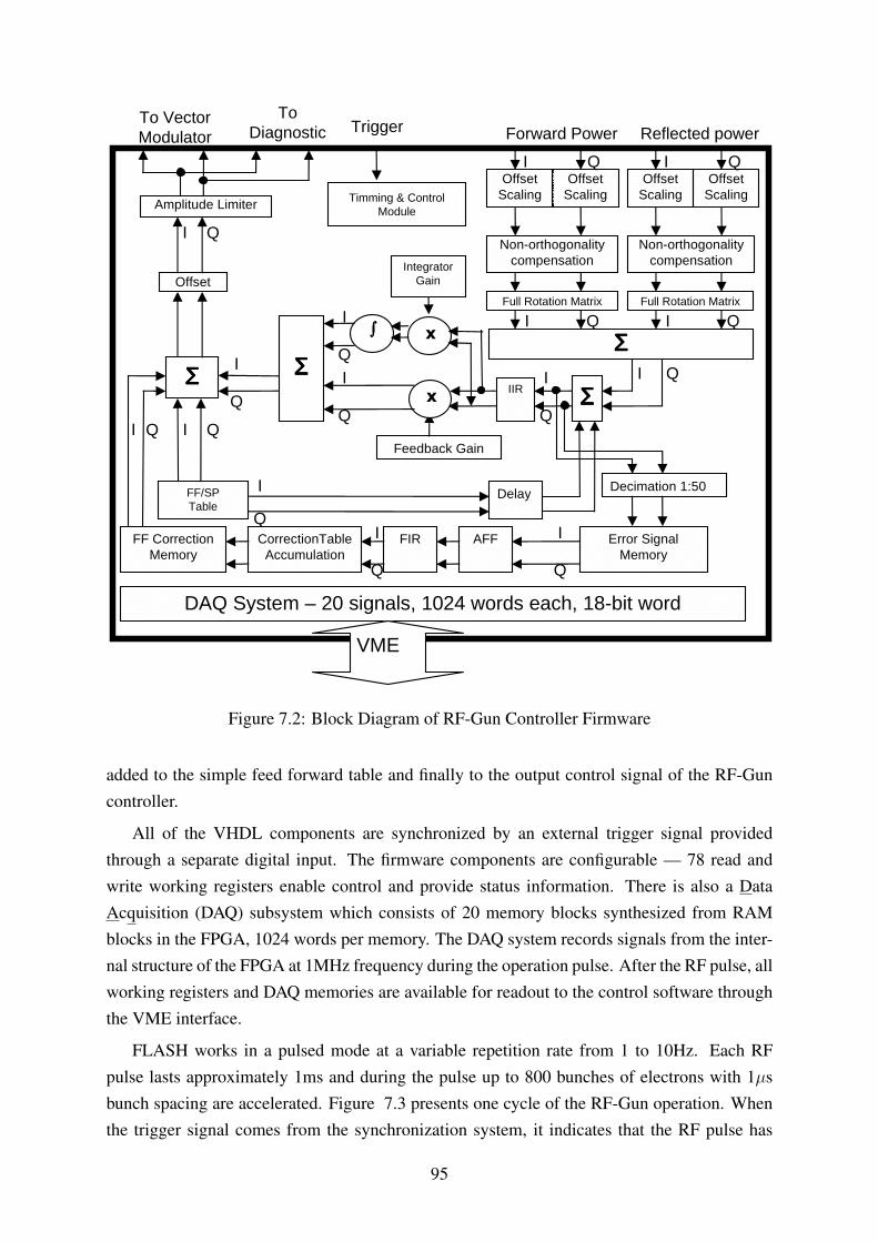
FF/SPTable
Feedback Gain
OffsetScaling
Full Rotation Matrix
Timming & ControlModule
To VectorModulator
xIIR
IntegratorGain
x∫∫∫∫
Non-orthogonalitycompensation
Non-orthogonalitycompensation
Full Rotation Matrix
Amplitude Limiter
To Diagnostic Trigger
I Q
Decimation 1:50
Error SignalMemory
FF CorrectionMemory
CorrectionTable Accumulation
FIR AFF
DAQ System – 20 signals, 1024 words each, 18-bit word
VME
ΣΣΣΣ
ΣΣΣΣ
Delay
ΣΣΣΣΣΣΣΣ I QI
Q
I
Q
I
QI
Q
I Q
I QI Q
I
Q
I
Q
I Q
Forward Power Reflected power
I
Q
Offset
I Q
OffsetScaling
OffsetScaling
OffsetScaling
I Q
Figure 7.2: Block Diagram of RF-Gun Controller Firmware
added to the simple feed forward table and finally to the output control signal of the RF-Guncontroller.
All of the VHDL components are synchronized by an external trigger signal providedthrough a separate digital input. The firmware components are configurable — 78 read andwrite working registers enable control and provide status information. There is also a DataAcquisition (DAQ) subsystem which consists of 20 memory blocks synthesized from RAMblocks in the FPGA, 1024 words per memory. The DAQ system records signals from the inter-nal structure of the FPGA at 1MHz frequency during the operation pulse. After the RF pulse, allworking registers and DAQ memories are available for readout to the control software throughthe VME interface.
FLASH works in a pulsed mode at a variable repetition rate from 1 to 10Hz. Each RFpulse lasts approximately 1ms and during the pulse up to 800 bunches of electrons with 1µsbunch spacing are accelerated. Figure 7.3 presents one cycle of the RF-Gun operation. Whenthe trigger signal comes from the synchronization system, it indicates that the RF pulse has
95

t
Trigger Triggerfrom 100ms to 500ms
1024us
RF Pulse
Interrupt
DAQ Readout
Stable field Field decayEnergyloading
Figure 7.3: One Cycle of RF-Gun Control
started. It lasts 1024µs. During the RF pulse, energy is loaded into the cavity and then RF-Guncontroller stabilizes the amplitude and phase of the field. The dashed line in figure 7.3 presentsshape of the field amplitude in the cavity. The bunches of electrons are emitted when the field isstable. After the beam has been injected the cavity is discharged what is presented in the figureas a field decay. During the RF pulse, the controller records several signals and stores themin the DAQ subsystem. When the RF pulse is finished, the controller generates an interruptto notify the control software that the DAQ data is ready. An interrupt handler routine inthe control software immediately reads data from the DAQ. The DAQ readout must be finishedbefore the trigger signal for the next RF pulse comes.
7.2 Adaptation of the RF-Gun Controller to VXI Systems
As was already mentioned, the existing RF-Gun controller works in a VME system. The leftside of figure 7.4 presents hardware and software of the existing setup. The SIMCON board isinstalled in a VME crate. The crate is controlled by an embedded computer installed in the slot1. This is a SUN machine with Solaris OS. The SIMCON driver runs on this computer and itcommunicates through the VME bus with working registers of the SIMCON board by exchang-ing binary data. Remote control of the RF-Gun controller is enabled by a server applicationrunning on the SUN machine which allows remote execution of the SIMCON driver routines.The user interacts with the client application which communicates with the server applicationover Ethernet.
The VXI version of the RF-Gun controller is presented on the right side of figure 7.4.A VXI module consisting of the SIMCON board and VXI-IC is installed in a VXI chassis.No embedded computer is required in this setup, only a VXI controller with a LAN interfaceon the front panel, which is installed in the slot 0. Unlike the VME version, the SIMCONSCPI driver is embedded in VXI-IC. The driver exchanges binary data with working registersof the RF-Gun controller. Instead of the client-server program in the VME version, a userprogram in the remote computer communicates directly with VXI-IC using the VISA library.
96

VME Crate
SIMCON
Control Algorithms
Working Registers
VME bus
Embedded
ComputerSIMCON Driver
Server Application
PC
Client Application
LAN
Binaries
Binaries
VXI Chassis
SIMCON
Control Algorithms
Working Registers
VXI bus
LAN/VXI Controller
PCUser Program
LAN
Binaries
VXI-MBTSIMCON SCPI Driver
SCPI
SCPI
VISA
User Program
Figure 7.4: Existing VME and proposed VXI version of RF-Gun controller
The user program exchanges SCPI messages with the SCPI driver in VXI-IC.
The general concept of the RF-Gun controller implementation in a VXI system is presentedin figure 7.5. There are four major features of VXI-MBT that are involved in adaptation of
InputOutput
Working Registers
DAQSystem
SynchronizationModule
VXI Bus
TriggerSubsystem
InterruptRequester
SCPIDriver
Direct MemoryAccess
SIMCON3.1
VXI-MBT
SCPI Binary data
Binary data
Binary data
TTLTRG IRQ*
Triggers DeviceInterrupt
RF-Gun controller algorithms
Figure 7.5: Concept of RF-Gun controller adaptation using VXI-MBT
97
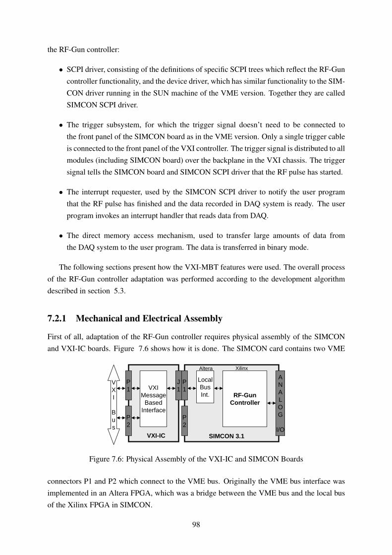
the RF-Gun controller:
• SCPI driver, consisting of the definitions of specific SCPI trees which reflect the RF-Guncontroller functionality, and the device driver, which has similar functionality to the SIM-CON driver running in the SUN machine of the VME version. Together they are calledSIMCON SCPI driver.
• The trigger subsystem, for which the trigger signal doesn’t need to be connected tothe front panel of the SIMCON board as in the VME version. Only a single trigger cableis connected to the front panel of the VXI controller. The trigger signal is distributed to allmodules (including SIMCON board) over the backplane in the VXI chassis. The triggersignal tells the SIMCON board and SIMCON SCPI driver that the RF pulse has started.
• The interrupt requester, used by the SIMCON SCPI driver to notify the user programthat the RF pulse has finished and the data recorded in DAQ system is ready. The userprogram invokes an interrupt handler that reads data from DAQ.
• The direct memory access mechanism, used to transfer large amounts of data fromthe DAQ system to the user program. The data is transferred in binary mode.
The following sections present how the VXI-MBT features were used. The overall processof the RF-Gun controller adaptation was performed according to the development algorithmdescribed in section 5.3.
7.2.1 Mechanical and Electrical Assembly
First of all, adaptation of the RF-Gun controller requires physical assembly of the SIMCONand VXI-IC boards. Figure 7.6 shows how it is done. The SIMCON card contains two VME
P1
P2
J1
P1
P2
ANALOG
I/O
VXIMessage
BasedInterface
LocalBusInt. RF-Gun
Controller
VXI
Bus
VXI-IC SIMCON 3.1
Altera Xilinx
Figure 7.6: Physical Assembly of the VXI-IC and SIMCON Boards
connectors P1 and P2 which connect to the VME bus. Originally the VME bus interface wasimplemented in an Altera FPGA, which was a bridge between the VME bus and the local busof the Xilinx FPGA in SIMCON.
98

In the VXI version, the Altera FPGA firmware is reprogrammed to provide only a bridgebetween the local bus in VXI-IC and the local bus in the Xilinx FPGA of the SIMCON board.The VXI-IC device interface was configured to the local bus mode. The Altera firmware alsocontains trigger and interrupt lines for interconnections between the Xilinx and the P1 connec-tor of SIMCON. Since the VXI-IC has only one 96-pin user connector, J1, the SIMCON boardwas connected only to the P1 connector. A picture of the physical assembly is presented infigure 7.7.
Figure 7.7: Picture of the Physical Assembly of the VXI-IC and SIMCON Boards
7.2.2 SCPI Driver for the RF-Gun Controller
The SCPI trees created for the RF-Gun controller cover its entire functionality except for theDAQ system. All software included in the existing SIMCON driver, which runs in a VMEsystem, was moved to the SIMCON SCPI driver located in VXI-IC. Figure 7.8 once againpresents the RF-Gun controller algorithms which are enclosed in five red areas. These redareas correspond to five SCPI trees which were defined for the controller.
99
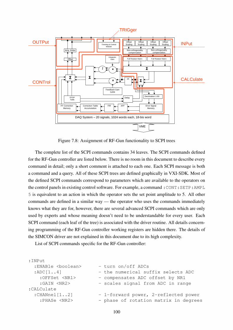
Non-orthogonalitycompensation
FF/SPTable
Feedback GainGAIN
OffsetScaling
Full Rotation Matrix
Timming & ControlModule
xIIR
IntegratorGain
x∫∫∫∫
OffsetScaling
OffsetScaling
OffsetScaling
Non-orthogonalitycompensation
Full Rotation MatrixOffset
Decimation 1:50
Error SignalMemory
FF CorrectionMemory
Correction Table Accumulation
FIR AFF
DAQ System – 20 signals, 1024 words each, 18-bis word
VME
ΣΣΣΣ
ΣΣΣΣ
Delay
ΣΣΣΣΣΣΣΣ
OUTPut
CONTrolCALCulate
INPut
TRIGger
Amp. limiter
Figure 7.8: Assignment of RF-Gun functionality to SCPI trees
The complete list of the SCPI commands contains 34 leaves. The SCPI commands definedfor the RF-Gun controller are listed below. There is no room in this document to describe everycommand in detail; only a short comment is attached to each one. Each SCPI message is botha command and a query. All of these SCPI trees are defined graphically in VXI-SDK. Most ofthe defined SCPI commands correspond to parameters which are available to the operators onthe control panels in existing control software. For example, a command :CONT:SETP:AMPL5 is equivalent to an action in which the operator sets the set point amplitude to 5. All othercommands are defined in a similar way — the operator who uses the commands immediatelyknows what they are for, however, there are several advanced SCPI commands which are onlyused by experts and whose meaning doesn’t need to be understandable for every user. EachSCPI command (each leaf of the tree) is associated with the driver routine. All details concern-ing programming of the RF-Gun controller working registers are hidden there. The details ofthe SIMCON driver are not explained in this document due to its high complexity.
List of SCPI commands specific for the RF-Gun controller:
:INPut:ENABle <boolean> - turn on/off ADCs:ADC[1..4] - the numerical suffix selects ADC
:OFFSet <NR1> - compensates ADC offset by NR1:GAIN <NR2> - scales signal from ADC in range
:CALCulate:CHANnel[1..2] - 1-forward power, 2-reflected power
:PHASe <NR2> - phase of rotation matrix in degrees
100

:OPHase <NR2> - non-orthogonality phase correction:FILTer <NR1> - corner frequency of the IIR filter
for error signal:CONTrol
:SETPoint - set point table parameters:AMPLitude <NR2> - amplitude of set point table in MW:PHASe <NR2> - phase of set point table in degress:TIME - set point table timing parameters
:FILLing <NR1> - length of filling timein microseconds
:FLATtop <NR1> - flat top time length in microseconds:DECay <NR1> - decay time length in microseconds
:DELay <NR1> - delays set point against feedforward table
:FFORward:ENABle <boolean> - enables feed forward table
:FBACk - proportional controller parameters:GAIN <NR2> - gain of proportional controller
in arbitrary units:ENABle <boolean> - enables feedback
:INTegrator - integrator parameters:GAIN <NR2> - gain of integrator:ENABle >NR2> - enables integrator
:AFForward:TCONstant <NR2> - cavity time constant:GAIN <NR2> - speed of adaptation:FILTer <NR1> - corner frequency of FIR filter
for correction signal:ENABle <boolean> - AFF enabled:MODE INFinite|STEPs - mode of operation:TRANGe
:STARt <NR1> - start of operation:STOP <NR1> - stop of operation:DELay <NR1> - delay of correction table
:OUTPut:ENABle <boolean> - AFF output enabled
:SMODe - switching mode of AFF and feedback:ENABle <boolean> - switching mode enabled:GSTeps <NR1> - number of feedback steps:AFFSteps <NR1> - number of AFF steps
:OUTPut:DAC[1..2] - the numerical suffix selects DAC
:OFFSet <NR1> - sets offset of DAC, thatcompensates offsetof vector modulator
:ALIMit - amplitude limiter parameters:ENABle <boolean> - enables amplitude limiter of
control signal
101
:AMPLitude <NR2> - sets amplitude limit:TRIGger
[:SEQuence[1..2]]:SOURce EXTernal|INTernal|TTLTrg[0..7] - selects source
of trigger signal:TIMer <NR1> - sets frequency in Hz of internal
trigger generated by timer:DELay <NR1> - trigger pulse delay in microseconds
The implemented SIMCON SCPI driver has several advantages. One of them is reducedtraffic on the VXI bus compared to the VME version. For example, the RF-Gun controllercontains 3 pairs of control tables which store imaginary and quadrature parts of the controlsignals, including the set point, feed forward, and proportional gain and integrator gain tables,see figure 7.8. In the VME-based version these tables were calculated by the SIMCON driverin the embedded SUN, see figure 7.4. When one of the control parameters has such as theamplitude or phase changed, the tables were recalculated in the SIMCON driver and sent tothe SIMCON board through the VME bus. Since each control table has 2048 elements, eachchange of the amplitude or phase by the user resulted in transmission at least of 2048 wordson the VME bus. For VXI-IC, the user program only needs to send a single SCPI messagewith the new amplitude or phase value, e.g. :CONT:SETP:AMPL 10 for set point amplitude,or :CONT:SETP:PHAS 130 for set point phase. The SIMCON SCPI driver receives thesecommands and calculates new control tables locally and writes them to the SIMCON boardthrough the local bus. After the SCPI command has been sent by the user program, the VXIbus is released. The calculation of new control tables is done by the SIMCON SCPI driver inparallel to other activities which may take place on the VXI bus.
The other advantages of the SIMCON SCPI driver are described in the following sections.
7.2.3 Application of the Trigger Subsystem
Originally the trigger signal was connected to the front panel of the SIMCON board and toevery other board installed in the VME crate. Each of these boards has a separate digital inputfor the trigger signal. For the VXI chassis, the trigger signal needs to be connected only tothe VXI controller located in the slot 0. The trigger signal is distributed on the VXI backplaneto all other modules in the same chassis. VXI-IC provides the trigger signal from the VXIbackplane to the SIMCON board through the device interface. Nevertheless, the other sourcesof the trigger signal for the SIMCON board can still be used, as explained below.
The specific SCPI commands related to the trigger subsystem are repeated here once againbecause they require a separate explanation:
:TRIGger
[:SEQuence[1..2]]
:SOURce EXTernal|INTernal|TTLTrg[0..7]
102

:TIMer <NR1>
:DELay <NR1>
As the parameters of the command :TRIGger:SEQuence:SOURce show, three sourcesof the trigger signal are possible:
• INTernal — the internal trigger is used in a laboratory environment when the exter-nal trigger is not provided. The internal trigger is generated by a local timer locatedinside the Synchronization Module, see figure 7.8. The :TRIG:SEQ:TIM <freq>
command sets the frequency of this trigger in units of Hertz.
• TTLTRG[0..7] — the external trigger from the synchronization system of FLASHis connected to the VXI controller. This trigger is distributed on the VXI backplane tothe SIMCON board. The parameter suffix selects which trigger line is used by the VXI-IC.
• EXTernal — choosing this option gives the possibility of using the trigger signal di-rectly connected to the SIMCON front panel as it was done in the VME version.
As was explained in section 6.1.3.6, when the trigger signal comes to VXI-IC, the PowerPCinterrupt is generated and the user interrupt handler routine is launched. In this case, the routinesets the flag Pending RF pulse which tells the SIMCON SCPI driver that no action can betaken on the working registers of the RF-Gun controller during the RF pulse — the operatingconditions of the RF-Gun controller must not changed during the RF pulse [67].
For the case of the external trigger (TTLTRG or EXTernal), it is necessary to delay the trig-ger pulse in order to be synchronized with other components of FLASH. The trigger pulse canbe delayed by several microseconds using the command :TRIG:SEQ:DEL <µs>.
7.2.4 Interrupt Generation and Handling
The RF-Gun controller in the VME version generates interrupts on the VME bus when the RFpulse is finished. These interrupts indicate that the data recorded during the RF pulse inthe DAQ system is ready to be read. The interrupt notifies the SIMCON driver in the SUNmachine and an appropriate interrupt handler routine is called. This routine reads the data fromthe DAQ system through the VME bus and makes it available to the server application, left sideof figure 7.4.
The SIMCON board cannot generate an interrupt directly on the VXI bus because it is notconnected to it. The VXI-IC also doesn’t allow for direct access from the SIMCON board tothe VXI interrupts. There is only one interrupt line wired from the SIMCON board to PowerPCin VXI-IC, as presented in figure 7.9. When this line is asserted by SIMCON, an interruptis generated in the PowerPC. As was already explained, a special interrupt handler routine,which is empty by default, is launched in PowerPC. The routine can be filled out by the devicedeveloper in VXI-SDK. In this example the routine generates an interrupt on the VXI bus.
103

VXI
Bus
InterruptRequester
VXI-IC
InterruptHandler Device Int
VXI Int
Timing&
Synchr.Module
SIMCONStatusByte
PowerPC
Figure 7.9: Configuration of Interrupts for RF-Gun Controller
The interrupt handler in the PowerPC writes a Status Byte to the VME interrupt requesterregister and stimulates it to generate an interrupt on the VXI bus by asserting the VXI Int line.The detailed description of the C routines for interrupt requester operation is in appendix D.8.
During the interrupt acknowledge process on the VXI bus, the VXI controller reads the Sta-
tus Byte and returns it to the control software. In this particular case, the user program isnotified through the mechanisms of the VISA library. A special routine in the user programreads the data from the DAQ memories.
7.2.5 Direct Access to DAQ Subsystem in RF-Gun Controller
As was described previously, the working registers are read and written from VXI-IC by the de-vice driver routines. Besides the working registers, the RF-Gun controller contains a DAQsystem with 20 memory blocks inside, see fig. 7.2. The blocks are used for recording sig-nals from the internal structure of the controller during the RF pulse, and after the pulse theyare read only. One can imagine that readout of the memory could be performed by a SCPIcommand. The readout of one block would return a vector of 1024 numbers formatted in onelong response string. The problem is that the readout of 20 block would take a long time dueto overhead related to the conversion of scalar values to strings in VXI-IC formatter and laterreverse conversion from strings to numbers in the control software. In order to bypass thisproblem, direct memory access was implemented in VXI-IC. According to the VXI specifi-cation the configuration and communication registers of VXI-IC are accessible in A16/D16mode on the VXI bus, but the working registers of SIMCON are not available on the VXI bus.The direct memory mechanism allows mapping a portion of the SIMCON address space di-rectly to the A24 or A32 address space on the VXI bus. The block diagram of the implementedmechanism is presented in figure 7.10.
According to the VXI specification, during the VXI system initialization process the VXI-ICrequests address space, in an amount set by the user in the configuration registers of VXI-ICusing VXI-SDK. The VXI controller allocates the requested address space by writing the baseaddress of that space to the configuration register in VXI-IC. VXI-IC automatically mapsthe base address of the DAQ memories in the context of the local bus to the base address previ-ously assigned. From that moment on, the address detector makes the VME slave active when
104

VXI
VMESlave
VXIRegs
LocalBus
Arbiter
PowerPC
SIMCONBoard
AddressDetector
Local Bus VME Bus
VXI-IC
A24/D16 A32/D32
Figure 7.10: Direct Memory Access from VXI to RF-Gun Controller
the DAQ readout is requested from the VXI bus. Since the VME slave component and PowerPCare masters to SIMCON in context of the local bus communication, an arbitration mechanismmust be applied. The local bus arbiter takes control when both the PowerPC and the VXISlave request access to SIMCON. The PowerPC has higher priority since the communicationis faster and shorter due to single reads and writes. However, if the access from the VXI bus toSIMCON is blocked for longer time than the VME bus timeout, the RETRY* signal on the busis asserted. The data bus between SIMCON and VXI-IC is 16 bits wide; only A24/D16 orA32/D16 access from the VXI bus is possible. Direct access to the memory area in SIMCONsignificantly speeds up the readout of large amounts of data from the SIMCON DAQ system.This is especially true for block transfers on the VXI bus.
7.3 Application Tests and Summary
The RF-Gun controller has been tested in a laboratory environment. A laboratory functiongenerator was connected to the trigger input in the VXI controller and distributed on the VXIbackplane to the RF-Gun controller. The external trigger signal was generated in this func-tion generator. Figure 7.11 presents a picture of the development setup for the RF-Gun con-troller. The VXI controller used in the experiment (Agilent E1406A) has no Ethernet socket onthe front panel. It has only a GPIB interface, for which a GPIB/LAN converter was used.
Figure 7.12 presents the control panel of the user program. This panel is very similar tothe existing one now used at FLASH. Preparation of such panels is relatively simple. Mostof the parameters located on the graphical panel relate to single SCPI commands defined forthe RF-Gun controller. When the value of a parameter is changed, the SCPI command stringis formulated and sent through the VISA library directly to the VXI-IC. The plots visible onthe right side of the panel are read using direct memory access. Due to limitations of the VisualBasic 6.0 language, the interrupts generated by the RF-Gun controller are detected by the userprogram in a queuing mode [37].
105

Figure 7.11: A Picture of the Development Setup for the RF-Gun Controller
Figure 7.12: Panel of the User Program for RF-Gun Controller
The entire functionality of the RF-Gun was successfully tested. The RF-Gun controller isready for experimental use in FLASH.
106
8
Conclusion and Hints for Successors
8.1 Conclusions
The VXI-MBT opens new possibilities for implementation of VXI message-based devices.A designer may easily integrate his specific electronics with other VXI devices in a reasonabletime. The following advantages make the usage of VXI-MBT attractive:
• short implementation time from specific electronics concept to 100% VXI message-baseddevice,
• full customization of SCPI trees,
• open source code of the device driver for device-specific SCPI commands,
• available user entry routines for interrupt handling and VXI-IC configuration,
• built-in implementations of obligatory IEEE 488.2 Common Commands, obligatory SCPIcommands and several others executed by the VXI-IC,
• independence from software solutions such as C-SCPI or I-SCPI, which have been dis-continued, and insensitivity to commercial driver concepts such as VXIplug&play or IVI,
• distribution of the system intelligence among particular devices, with each message-based device able to process SCPI commands locally in a concurrent mode, thus reducingthe load on the central computer or command module,
• a development stage for message-based devices which can be separated from the appli-cation stage.
Unfortunately, besides a number of advantages the potential user needs to be aware ofseveral disadvantages:
• message-based devices are in general slower than register-based, however, the computa-tion overhead in a PC for a pseudo message-based device is also significant,
107

• the hardware resources required for implementation of the SCPI parser and decoder aremore expensive than implementation of equivalent software in a computer.
8.2 Universality of IEEE 488.2 and SCPI — Toward LXI
The presented tool is designed for message-based devices in the VXI standard. That wasthe most natural implementation due to the clear definition of the VXI device compliant tothe IEEE 488.2 standard. The implemented message exchange control interface and mes-sage exchange protocol originate from IEEE 488.2 based on the IEEE 488.1 bus. But onecan imagine implementation of message-based devices in other standards such as PXI or LXI.Both are standards for instrumentation, and both implement a kind of hardware trigger bus.The PXI standard doesn’t define a message-based device; aside from a few obligatory con-figuration registers, the communication protocol is device dependent in the PXI standard. Insome applications, a PXI device could communicate using SCPI messages. The LXI standardincludes rule 10.1 which says that VXI-11 protocol shall be supported by all LXI devices fordiscovery purposes [26]. The derived rules say that each LXI device shall be able to respond tothe *IDN? IEEE 488.2 Common Command but all SCPI commands are optional. Neverthelesssuch a device could also interpret any SCPI messages.
In order to develop a SCPI message-based device for PXI or LXI, one could use the VXI-MBTimplementation as a basis. In both cases the bus interface and the trigger control block wouldhave to be exchanged. Figure 8.1 presents once again the block diagram of the VXI-MBTmodel with the blocks, which have to be exchanged marked, by a dashed rectangle.
VXI InterfaceFixed part
Message Exchange
Control
Parser, Formatter of IEEE 488.2 Syntax ( Interprets (Interprets
obligatory commands) specific SCPI commands)�
Execution Control Tool Driver Device Driver
(Executes obligatory (Executes specificcommands) SCPI commands)�
Device Interface(Physical ( Configurable
connector) specific protocol)
Trigger Control(Configurable)�
IC
User Device
I/O Library
PC
SDK-Trigger Control Configuration- SCPI Trees Definition- Source Code for Device Driver- User Device Interface Configuration
IEEE 488.1, PXI, LXI
Figure 8.1: VXI-MBT for Alternative Instrumentation Buses
Of course, this requires modification of hardware, because the VXI interface would have tobe replaced by a PXI interface, or an Ethernet socket for LXI. In both cases, the interface to
108

the trigger subsystem would also have to be modified due to electrical and logical differences.Nevertheless, the presented realization of VXI-MBT could be an inspiration for further
development of message-based tools for measurement and control systems.
109

110
References
[1] Deutsches Elektronen-Synchrotron. Notkestrasse 85, 22607 Hamburg, Germany.[Online]. Available: http://www.desy.de
[2] The European X-Ray Free-Electron Laser - Technical design report, DESY XFEL ProjectGroup, Jul. 2006. [Online]. Available: http://www.xfel.desy.de
[3] Koprek W., Grecki M., Makowski D., Pawlik P., Weddig H., Lorbeer B., Hoffmann M.,Mukherjee B., Czuba K., Koseda B., Cichalewski W., Pozniak K. T., Romaniuk R. S.,Simrock S., “Status of LLRF system development for european XFEL,” in Proceedings
of SPIE, vol. 6347, 2006, pp. 634 703–1–18.
[4] Jałmuzna W., Koprek W., Pucyk P., Simrock S., “FPGA-based implementation of a cavityfield controller for FLASH,” IOP — Institute of Physics, vol. 6347, pp. 122–129, 2006.
[5] IEEE Standard 488–1978: IEEE Digital Interface for Programmable Instrumentation,IEEE, Inc. Std., Rev. II, Nov. 1978.
[6] IEEE 488.1–1987: IEEE Digital Interface for Programmable Instrumentation , IEEE,Inc. Std., Jun. 1987.
[7] IEEE Std 488.2–1992: IEEE Standard Codes, Formats, Protocols, and Common Com-
mands, IEEE, Inc. Std., Dec. 1992, For Use With IEEE Std 488.1–1987.
[8] Nawrocki W., Rozproszone systemy pomiarowe, 1st ed. Wydawnictwo Komunikacji iŁacznosci, 2006, ch. 5.4.6.
[9] Versabus Specification Manual, Motorola, Inc. Std., Rev. M68KVBS(D4), May 1981.
[10] IEC 60297-3–101 Mechanical structures for electronic equipment Dimensions of mechan-
ical structures of the 482,6 mm (19 in) series Part 3-101: Subracks and associated plug-in
units, International Electrotechnical Commission Std., Aug. 2004.
[11] IEC 60603-2 Connectors for Frequencies Below 3 MHz for Use with Printed Boards —
Part 2: Detail Specification for Two-Part Connectors with Assessed Quality, for Printed
Boards, for Basic Grid of 2,54 mm (0,1 in) with Common Mounting Features, InternationalElectrotechnical Commission Std., Jan. 1995.
111

[12] American National Standard for VME64, Revision 3.0, VMEbus International Trade As-sociation Std., Apr. 1995.
[13] VXI-1 System Specification, VXIbus Consortium Std., Rev. 2.1, Aug. 1998. [Online].Available: www.vxi.org
[14] Charuba J., “Development of Modular Electronics Standards for High Energy PhysicsExperiments,” in Proceedings of International Workshop "Relativistic Nuclear Physics
from Hundreds MeV to TeV", Varna, Bulgaria, 2001.
[15] VXI-1 System Specification, VXIbus Consortium Std., Rev. 3.0, Nov. 2003. [Online].Available: www.vxi.org
[16] Standard Commands for Programmable Instruments(SCPI), SCPI Consortium Std., May1999. [Online]. Available: www.scpiconsortium.org
[17] Mielczarek, W., Urzadzenia pomiarowe i systemy kompatybilne ze standardem SCPI,1st ed. HELION, Poland, 1999, ch. 2.
[18] VXIPlug&Play, System Alliance Std., Dec. 1993. [Online]. Available:http://www.vxipnp.org
[19] Interchangeable Virtual Instrument, IVI Foundation Std., Oct. 2006. [Online]. Available:http://www.ivifoundation.org
[20] PICMG c/o Virtual, Inc. 401 Edgewater Place, Suite 600 Wakefield, MA 01880 USA.[Online]. Available: http://www.picmg.org
[21] PCI Express 2.0, Base Specification, PCI-SIG Std., Rev. 0.9, Sep. 2006. [Online].Available: http://www.pcisig.com
[22] PXI-5: PXI Express Hardware Specification, PXI System Alliance Std., Rev. 1.0, Aug.2005. [Online]. Available: http://www.pxisa.com
[23] IEEE 802.3-2005: Local and metropolitan area networks — Specific requirements, IEEE,Inc. Std. ISBN 0-7381-4741-9, Dec. 2005. [Online]. Available: http://www.ieee.org
[24] Kopp, S., “Using Precision Time Protocol with LXI,” Agilent Measurement Journal, vol.Issue 1, 2007.
[25] Parkinson B.W., Global Positioning System: Theory and Applications. American Insti-tute of Aeronautics and Astronautics, Washington, D.C., 1996, ch. Chap. 1: Introductionand Heritage of NAVSTAR, the Global Positioning System, pp. 3–28.
[26] LXI Standard, LXI Consortium Std., Rev. 1.2, Oct. 2007. [Online]. Available:www.lxistandard.org
112

[27] Agilent E8491B IEEE 1394 PC Link to VXI Configuration and User’s Guide, 2nd ed.,Agilent Technologies, Inc., Feb. 2006.
[28] USB 2.0 to VXIbus Interface, VXI-USB, VXI Technologies, Inc., datasheet. [Online].Available: www.vxitech.com
[29] Agilent E1406A Command Module, User’s Manual and SCPI Programming Guide,Agilent Technologies, Inc. [Online]. Available: www.agilent.com
[30] Agilent E1482B VXI-MXI Bus Extender, User’s Manual, 5th ed., Agilent Technologies,Inc, 2006.
[31] MXIbus Multisystem Extension Interface Bus Specification, Version 2.0, Apr. 1997.[Online]. Available: http://www.ni.com
[32] LXI-VXI Gigabit Ethernet Slot 0 Interface, User’s Manual, P/N: 82-0115-000 ed., VXITechnologies, Inc., Feb. 2007.
[33] VXIpcTM 770/870B Series, User Manual, 370381st ed., National Instruments, Inc., Jun.2004.
[34] Winiecki W., Rozproszone systemy pomiarowe — wykład, Instytut SystemówElektronicznych, Politechnika Warszawska.
[35] Agilent IO Libraries Suite, Agilent E2094N, Agilent SICL User’s Guide, 7th ed., AgilentTechnologies, Inc., Oct. 2004. [Online]. Available: http://www.agilent.org
[36] Test & Measurement Systems, Inc. [Online]. Available: http://www.tamsinc.com/
[37] Agilent IO Libraries Suite, Agilent E2094N, Agilent VISA User’s Guide, AgilentTechnologies, Inc., Oct. 2004. [Online]. Available: http://www.agilent.com
[38] VPP-4.3.4, VISA Implementation Specification for COM, VXIPlug&Play SystemAlliance Std., Rev. 3.1, Jan. 2007. [Online]. Available: http://www.vxipnp.org
[39] VPP-3.1, Instrument Drivers Architecture and Design Specification, VXIPlug&PlaySystem Alliance Std., Rev. 4.1, Dec. 1998. [Online]. Available: http://www.vxipnp.org
[40] IVI-3.1: Driver Architecture Specification, Revision 1.0, IVI Foundation Std., Mar. 2002.[Online]. Available: http://www.ivifoundation.org
[41] HP Compiled SCPI for HPUX, 4th ed., Hewlett-Packard, Inc., Nov. 1994.
[42] “Test-System Development Guide, Understanding Drivers and Direct I/O,” Agilent Tech-nologies, Inc., Jan. 2004, Application note No. 1465-3.
113

[43] Hejn K.W., Systemy pomiarowe — wykład, Instytut Systemów Elektronicznych,Politechnika Warszawska.
[44] Test-System Development Guide, Using SCPI and Direct I/O vs. Drivers, Agilent Tech-nologies, Dec. 2004, Application note No. 1465-13.
[45] Clary, A., “IVI drivers: Slower but simpler,” Test and Measurement World, vol. 2/1/2003,2003.
[46] Kopp S., “Using IVI-COM: The Top Ten Things You Need To Know,” Agilent Measure-
ment Journal, vol. Issue 1, 2007.
[47] IT9010M — VXIbus Message-Based Interface Chip, Interface Technology, Inc., Apr.2000. [Online]. Available: http://www.interfacetech.com
[48] Interface Technology, Inc. [Online]. Available: www.interfacetech.com
[49] VM9000 Single-slot Base Unit – Datasheet, VXI Technology, Inc. [Online]. Available:www.vxitech.com
[50] VM7000, VMIP Breadboard – User’s Manual, P/N: 82-0040-000 ed., VXI Technology,Inc., Apr. 2005.
[51] Message Based Prototyping Module 7064M – User’s Manual, Racal Instruments, Inc.,Feb. 2002, No. 980820.
[52] VXI-5526 Interface Card – Product Datasheet, ICS Electronics, Inc. [Online]. Available:www.icselect.com
[53] Mueller, J.E., “Efficient Instrument Design Using IEEE 488.2,” IEEE Transactions on
Instrumentation and Measurement, vol. IM-39, pp. 146–150, 1990.
[54] Winiecki W., Organizacja komputerowych systemów pomiarowych. OficynaWydawnicza Politechniki Warszawskiej, 1997, ch. 8.1.2, pp. 210–235.
[55] Carlson L.L., Willis W.H., “The VXIbus in a manufacturing test environment - VME-bus Extensions for Instrumentation, Standard Commands for Programmable Instruments- Technical,” Hewlett-Packard Journal, pp. 46–47, Apr. 1992.
[56] Koprek W., Hejn K.W., “Uniwersalne narzedzie elektroniczne wspomagajace projek-towanie przyrzadów komunikatowych VXI,” Przeglad Elektrotechniczny, vol. 5/2008,ISSN 0033-2097, pp. 249–254, 2008.
[57] Virtex-II Pro and Virtex-II Pro X FPGA User Guide, Xilinx, Inc., 2007, UG012 v4.2.[Online]. Available: www.xilinx.com
114

[58] PowerPC User’s Guide, Xilinx, Inc., 2006, uG018 v1.5. [Online]. Available:www.xilinx.com
[59] System ACE, Compact Flash Solution, Xilinx, Inc., 2002, DS080 v1.5. [Online].Available: www.xilinx.com
[60] Koprek W., Hejn K.W., “A flexible electronic tool for VXI register-based device devel-opment,” in Proceedings of SPIE, vol. 5948, 2005, pp. 81–90.
[61] Koprek W., Hejn K.W., “Inteligentny interfejs VXI dla elektroniki sterownika wnek re-zonansowych SIMCON 3.1,” PAR - Pomiary Automatyka Robotyka, vol. 7-8/2006, pp.17–20, 2006.
[62] Koprek W., “Narzedzie programowe do projektowania i testowania drzew rozkazówSCPI,” PAK - Pomiary Automatyka Kontrola, vol. 9 bis/2006, pp. 149–152, 2006.
[63] Brandt A., Hoffmann M., Koprek W., Pucyk P., Pozniak K.T., Romaniuk R.S., SimrockS., “Measurement and control of field in RF GUN at FLASH,” in Proceedings of SPIE,vol. 6937, 2007, pp. 69 370E1–6.
[64] Deutsches Elektronen-Synchrotron. Notkestrasse 85, 22607 Hamburg, Germany.[Online]. Available: http://www.flash.desy.de
[65] Giergusiewicz W., Jałmuzna W., Pozniak K.T., Ignashin N., Grecki M., Makowski D.,Jezynski T, Perkuszewski K., Czuba K., Simrock S., Romaniuk R.S., “Low latency controlboard for LLRF system: SIMCON 3.1,” in Proceedings of SPIE, vol. 5948, 2005, pp.59 482C1–6.
[66] Vogel E., Koprek W., Pucyk P., “FPGA Based RF Field Control at the Photo CathodeRF Gun of the DESY Vacuum Ultraviolet Free Electron Laser,” in Proceedings of EPAC,2006, pp. 1456–1458.
[67] Koprek W., Hejn K.W., “Implementation of the RF-Gun Controller as a Message-basedDevice in VXI Systems,” in Proceedings of the 15th International Conference MIXDES,2008, pp. 121–126.
[68] Mielczarek, W., SCPI, 1st ed. HELION, Poland, 1999.
[69] ANSI X3.42-1975, American National Standard Representatin of Numeric Values in Char-
acter Strings for Information Interchange, ANSI, 1975.
115

116

Appendix A
VXI Form Factors
C
A
B
D
P1
P1
P2
P1
P2
P1
P2
P3
3U
6U 6U
9U
One Rack Unit1U = 1.75 inch
A & B Defined by VME
C & DDefined by VXI
Figure A.1: VME and VXI Form Factors
117

118

Appendix B
Syntax of SCPI Messages
Regardless of its functionality, measurement devices perform some typical operations such asconditioning of measured signal, analog to digital conversion, digital signal processing, presen-tation of results, interfacing, storage of data, triggering and signal generation [68]. All theseoperations are reflected by functional blocks of the signal model of a SCPI device in figure B.1.
ROUTeinput
INPut SENSe CALCulate FORMat
ROUTeoutput
OUTput SOURce CALCulate FORMat
TRIGer MEMory DISPlay
Measurement Function
Signal Generation Function
DataFrom Bus
Data to Bus
Signalsfrom UUT
Signalsto UUT
Figure B.1: Signal Model of a SCPI Device
In principle, there are two major blocks of a device: measurement functions and signalgeneration functions. Depending on the device functionality both or one of them may be im-plemented. The measurement part consists of the following blocks:
• INPut — The purpose of this block is conditioning of the input signals before they areconverted by the SENSe block. Conditioning may include amplification, attenuation,linearization, filtering, frequency conversion, signal range adjustment, etc.
• SENSe — The SENSe block converts input signals into an internal data understandableby further blocks. This is usually analog to digital conversion. Several parameters maybe controlled in this block such as resolution or sampling frequency.
119
• CALCulate — This digital block performs mathematical operations on the converteddata. The purpose of these calculations is to extract required information from measureddata, e.g. time and amplitude calculation from the waveform. This is a part of the devicewhere its intelligence exists. The measured data can be processed to shorter form whichmay significantly reduce communication on a bus, e.g. singular rms value instead ofM-length record of samples.
Signal generation part consists of the following blocks:
• OUTput — This block is used for conditioning of signals generated by the device. Thisblock includes filtering, offsetting, power fitting, etc.
• SOURce — The SOURce block is responsible for generation of the output signals basedon parameters provided by the digital part of the device. This block may include digitalto analog converters. It is required for all source devices. It may include generator ofwaves, patterns, impulses, etc.
• CALCulate — This block is used to convert an application data into parameters under-standable for the SOURce block. Application parameters for waveforms generation maybe expressed in different domains and units. The intelligence of CALCulate block maybe used for generation of big amount of data from a few parameters. For example fourparameters is enough to generate any sine wave. This kind of operations reduce trafficon a bus. The CALCulate block helps in decentralization of the system intelligence.
In addition each device must contain digital interface for exchanging messages and externalport for interacting with a unit under test (UUT):
• FORMat — This part of the device is responsible for message exchanging with userapplications. This is usually some sort of digital interface such as VXI, RS232 or GPIB.This block is also used for data compression.
• ROUTe — is responsible for signal routing between UUT and measurement or genera-tion part the SCPI device. This is an optional feature of the SCPI device. It is used whererouting between physical ports and internal functional blocks of the SCPI device is pro-grammable. For example, a multimeter can be configured as voltmeter, current meter,ohmmeter, frequency meter, power meter, etc.
There are also several common blocks both for signal measurement and generation. They areoptional, but when applied, may extend the SCPI device functionality:
• TRIGger — The purpose of this block is to provide a device with a synchronizationcapability. The SOURce or SENSe blocks of the device can be synchronized by the com-mands (software method) or by internal, external signals (hardware method). The TRIG-ger block is responsible for proper configuration of the event sensors in order to receivethe synchronization signals.
120

• MEMory — The MEMory block is usually used to record measured data until it may beread by the user program. The MEMory block can be also used for storage of arbitrarypatterns which are used by the SOURce block.
• DISPlay — This block is used for presentation of measurement data in a textual or graph-ical manner. The DISPlay may interact with the user to achieve appropriate presentationof the data. The data manipulation by the DISPlay has no influence on data returned tothe user program.
Each block of the SCPI device model corresponds to a SCPI command subsystem. A SCPIcommand consists of one or more elements called mnemonics. The mnemonic is representedin a short or long version. Short version is written with capital letters and long one with smallletters. The subsequent series of the mnemonics form the SCPI command. The mnemonicsare separated by a colon. All mnemonics are grouped into trees. The command is createdstarting in the root of the three and going down to one of the leaves. Figure B.2 presentspart of the TRIGger tree. A command in square brackets represents the default mnemonic ona given level. The default node can be omitted while a command is constructed. For the SCPIparser, the missing mnemonic in the command means the default one. At the given level ofa SCPI tree only one default command is allowed. If the command or mnemonic representan element of the device which has several physical instances then the numerical suffix is addedto the mnemonic. It is used for indexing of particular instances. The mnemonic SEQuence infigure B.2 is an example of the default and multiple mnemonic.
:TRIGger
[:SEQuence[1..4]] :SOURce :TIMer
[:IMMediate] :LEVel :SIGNal
:AUTO
Figure B.2: Example of SCPI Tree
The SCPI command can be followed by one or more parameters separated from the com-mand by a white space. The command parameters are separated from each other by comas.There is no coma after the last parameter. SCPI uses parameter types defined by the IEEE488.2 standard, such as characters, decimal numbers, boolean values, block of data, and ex-pressions. In addition, the numeric values may be followed by units. The unit can consist ofa unit name and a multiplier which has impact on the preceding parameter value. The parame-ters may be obligatory or optional; may appear zero, one or several times depend on how theywere defined.
Each SCPI command is simultaneously a query until it is stated differently in the commanddefinition. The query has the same form as the corresponding command but it is followed
121

by a question mark. A device which interprets query must return a response to the controlsoftware. The response is also precisely defined in the command definition.
The advantage of SCPI is that it is a “living” industrial standard. Additional commands willalways be needed to meet the requirements of new technologies and new devices. The SCPIConsortium earlier, and IVI Foundation now, meets regularly to review new proposed com-mands and to approve extensions to the last version of the SCPI specification. New commandsmay be proposed by the members of the Consortium, and by other parties interested. Proposalsaccepted by the Consortium are published and distributed to member companies and are avail-able for the immediate use. Approved proposals are reviewed annually. After the annual review,a new revision of the SCPI standard is published, and the commands become a permanent partof the standard.
122

Appendix C
Model of IEEE 488.2 Device
This appendix presents concept of the device defined by the IEEE 488.2 standard. The twofigures below are replications of the original figures from the standard, but the IEEE 488.1bus was replaced by the VXI bus. The I/O control block in both diagrams is a VXI interface.The figure C.1 presents a general overview of a device status and message exchange.
I/OControl
MessageExchangeInterface
StatusReporting
DeviceFunctions
VXI Bus
Device status
Status message
IEEE 488.1 STB,IEEE 488.1 ist,IEEE 488.2 reqtand reqfmessages
IEEE 488.1device –dependentMessages and get
IEEE 488.1remotemessages
Figure C.1: Device Status and Message Exchange Overview
Figure C.2 presents a message exchange control interface defined by IEEE 488.2. Thisfigure presents details of the message exchange interface component from figure C.1. Thiskind of interface must be implemented in VXI message-based devices compliant with IEEE488.2. The implementation of this interface definitely requires some kind of local intelligencein the device. First of all, the complexity of the VXI message-based device interface is wrappedin the small I/O control box in figure C.2. Several rules and conditions defined by the VXIstandard must be fullfiled concerning the bus communication, configuration and communica-tion registers, device state, interrupts requesters and handling, triggering, etc. The second hugechallenge for the developer is implementation of the SCPI parser and response formatter. These
123

two blocks must be able to fulfill syntax rules defined in IEEE 488.2. All of this must be man-aged by the message exchange control which is driven by events. It must follow appropriatestate diagram in order to avoid deadlocks which lead to system failures.
VXIbus
I/O Control
STB,reqt,reqf, ist
MAV
Message Exchange Control
Output Queue Input Buffer
DAB END GET
clear clear
oq-full oq-empty
Ib-empty ib-full
get RMT-sent
bav brq dcas
Response Formatter
Parser
reset reset
rf-blockedeom, query p-blocked
Response Message Elements
DAB END GET
Device Functions
ponResponse Data
Query Error
Execution Control
Parsed Message Elements
ec-blocked
reset
Executable Message Elements
Command Error
Execution Error
Trigger Control
p-idle, ec-idle, ib-empty
tigger
p-idle
get
GET
ec-idle
Figure C.2: Message Exchange Control Interface Functional Blocks
124

Appendix D
VXI-MBT Features and Functionality
D.1 List of IEEE 488.2 Common Commands Supported byVXI-MBT
The VXI-MBT implements by default only 13 obligatory IEEE 488.2 Common Commandslisted in table D.1. The commands are implemented according to the IEEE 488.2-1987 speci-fication.
Mnemonic Description*CLS Clear Status Command*ESE Standard Event Status Enable Command*ESE? Standard Event Status Enable Query*ESR? Standard Event Status Register Query*IDN? Identification Query*OPC Operation Complete Command*OPC? Operation Complete Query*RST Reset Command*SRE Service Request Enable Command*SRE? Service Request Enable Query*STB? Read Status Byte Query*TST? Self-Test Query*WAI Wait-to-Continue Command
The execution routines of these functions are located in the VXI-IC driver and the userhas no access to the source code. However, the behavior of some of these commands dependson a user device. Thus, there are three user entry routines associated with the commands inbold: *CLS, *RST and *TST?. These routines are part of the device driver. They are emptyby default and can be fill out by the device developer according to his needs. These userentry routines are executed right after VXI-IC driver routines associated with these commands.The developer can edit these routines in the same way as the other regular driver routine forthe device-specific commands.
125

D.2 List of SCPI Commands Supported by VXI-MBT
The following list presents SCPI commands supported by the VXI-MBT by default. Part ofthem is defined as obligatory commands by the SCPI specification, [17], section 4.2.1.
:SYSTem - details: SCPI spec., section 21:ERRor
:ALL? - returns all err. codes with messages:CODE
:ALL? - returns all errors codes[:NEXT]? - retursn next error from the~queue
:COUNt? - returns number of errors in queue[:NEXT]? - rturns next error with message
:STATus - details: SCPI spec., section 20:OPERation
[:EVENt]? - returns content of event reg.:ENABle - enables bits in event reg.:ENABle? - returns status of enabled bits:PTRansition <NR1> - sets bit sensor to positive slope:NTRansition <NR1> - sets bit sensor to negative slope:CONDition <NR1> - returns content of condition reg.
:QUEStionable[:EVENt]? - returns content of event reg.:ENABle - enables bits in event reg.:ENABle? - returns status of enabled bits:PTRansition <NR1> - sets bit sensor to positive slope:NTRansition <NR1> - sets bit sensor to negative slope:CONDition <NR1> - returns content of condition reg.
:PRESet - sets initial values of above regs.:DIAGnostic - VXI-IC specific commands
:FLASh - CF card:UPLoad <String>, <ABPD> - loads file to CF card
:BOOT - reboot VXI-IC:UDEVice - user device
:INTerrupt:ENABle <Boolean> - enables interrupt from user dev.:ENABle? - returns status of user dev. intr.
:INSTrument - VXI-IC specific commands:INTerface - configuration of dev. interface
:BITMode[0..63] - general purpose I/O mode:VALue <Boolean> - sets one bit:VALue? - reads status of one bit
:LOCalbus - local bus mode:READ? <NR1> - reads reg. from user device:WRITe <NR1>, <NR1>- writes reg. to user device
:BUFFer - used in general purpose I/O mode:DIRection? - returns direction of user lines
126

:ENABle? - returns enabled buffers in dev. int.:ABORT - resets trigger system, SCPI spec.:ARM - details: SCPI spec., section 24
[:SEQuence[1..8]][:IMMediate] - immediately transits to INIT state:SOURce? - returns source of trigger:SOURce TTLTRG[0..7]|ECLTRG[0..1]|INTernal
:INITiate[:IMMediate] - immediately transits to ARM state
:TRIGger[:SEQuence[1..8]]
[:IMMediate] - immediately transits to dev. act.:SOURce? - returns source of trigger:SOURce TTLTRG[0..7]|ECLTRG[0..1]|INTernal
:OUTput - trigger source:ECLTrg[0..1] - selects ECL line
[:IMMediate] - generatse immediately a pulse:LEVel? - returns level of ECL line:LEVel <Boolean> - sets level of ECL line:STATe? - returns state of the~trg. source:STATe <Boolean> - enables trg. source
:TTLTrg[0..7] - selects TTL line[:IMMediate] - generatse immediately a pulse:LEVel? - returns level of TTL line:LEVel <Boolean> - sets level of ECL line:STATe? - returns state of the~trg. source:STATe <Boolean> - enables trg. source
All commands in the :DIAGnostic and :INSTrument trees are specific commands forVXI-IC.
The :SYSTem, :STATus trees are defined in the SCPI specification. Only these twotrees contain SCPI obligatory commands.
The :ABORT, :ARM, :INITiate, :TRIGger trees are used for the trigger subsys-tem. All of them are defined in the SCPI specification.
The :OUTput tree contains VXI-IC specific commands for TTLTRG and ECLTRG triggersource.
127
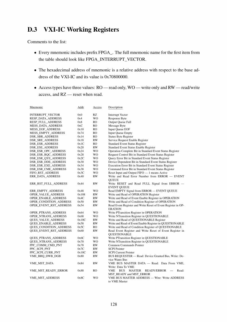
D.3 VXI-IC Working Registers
Comments to the list:
• Every mnemonic includes prefix FPGA_. The full mnemonic name for the first item fromthe table should look like FPGA_INTERRUPT_VECTOR.
• The hexadecimal address of mnemonic is a relative address with respect to the base ad-dress of the VXI-IC and its value is 0x70800000.
• Access types have three values: RO — read only, WO — write only and RW — read/writeaccess, and RZ — reset when read.
Mnemonic Addr Access Description
INTERRUPT_VECTOR 0x0 RZ Interrupt VectorRESP_DATA_ADDRESS 0x4 WO Response ByteRESP_FULL_ADDRESS 0x8 RO Output Queue FullMESS_DATA_ADDRESS 0xC RO Message ByteMESS_EOF_ADDRESS 0x10 RO Input Queue EOFMESS_EMPTY_ADDRESS 0x74 RO Input Queue EmptyDSR_SBR_ADDRESS 0x14 RO Status Byte RegisterDSR_SRE_ADDRESS 0x18 RW Service Request Enable RegisterDSR_ESR_ADDRESS 0x1C RO Standard Event Status RegisterDSR_ESE_ADDRESS 0x20 RW Standard Event Status Enable RegisterDSR_ESR_OPC_ADDRESS 0x24 WO Operation Complete Bit in Standard Event Status RegisterDSR_ESR_RQC_ADDRESS 0x28 WO Request Control Bit in Standard Event Status RegisterDSR_ESR_QYE_ADDRESS 0x2C WO Query Error Bit in Standard Event Status RegisterDSR_ESR_DDE_ADDRESS 0x30 WO Device Dependent Bit in Standard Event Status RegisterDSR_ESR_EXE_ADDRESS 0x34 WO Execution Error Bit in Standard Event Status RegisterDSR_ESR_CME_ADDRESS 0x38 WO Command Error Bit in Standard Event Status RegisterFIFO_RST_ADDRESS 0x3C WO Reset Input and Output FIFO — 1 means ActiveERR_DATA_ADDRESS 0x40 RW Write and Read Error Number from ERROR — EVENT
QUEUEERR_RST_FULL_ADDRESS 0x44 RW Write RESET and Read FULL Signal from ERROR —
EVENT QUEUEERR_EMPTY_ADDRESS 0x48 WO Read EMPTY Signal from ERROR — EVENT QUEUEOPER_VALUE_ADDRESS 0x108 RW Write and Read of OPERATION RegisterOPER_ENABLE_ADDRESS 0x4C RW Write and Read of Event Enable Register in OPERATIONOPER_CONDITION_ADDRESS 0x50 RW Write and Read of Condition Register of OPERATIONOPER_EVENT_RST_ADDRESS 0x54 RW Read Event Register and Write Reset of Event Register in OP-
ERATIONOPER_PTRANS_ADDRESS 0x64 WO Write PTransition Register in OPERATIONOPER_NTRANS_ADDRESS 0x68 WO Write NTransition Register in QUESTIONABLEQUES_VALUE_ADDRESS 0x10C RW Write and Read of QUESTIONABLE RegisterQUES_ENABLE_ADDRESS 0x58 RW Write and Read of Event Enable Register in QUESTIONABLEQUES_CONDITION_ADDRESS 0x5C RO Write and Read of Condition Register of QUESTIONABLEQUES_EVENT_RST_ADDRESS 0x60 RW Read Event Register and Write Reset of Event Register in
QUESTIONABLEQUES_PTRANS_ADDRESS 0x6C WO Write PTransition Register in QUESTIONABLEQUES_NTRANS_ADDRESS 0x70 WO Write NTransition Register in QUESTIONABLEPPC_COMM_CMD_PNT 0x78 RW Common Commands PointerPPC_SCPI_PNT 0x7C RW SCPI PointerPPC_SCPI_CURR_PNT 0x10C RW SCPI Current PointerVME_BRQ_DWB_DGB 0x80 RW BUS REQUESTER — Read: Device Granted Bus, Write: De-
vice Wants BusVME_MST_DATA 0x84 RW VME BUS MASTER DATA — Read: Data From VME,
Write: Data To VMEVME_MST_READY_ERROR 0x88 RO VME BUS MASTER READY/ERROR — Read:
MST_READY and MST_ERRORVME_MST_ADDRESS 0x8C WO VME BUS MASTER ADDRESS — Wire: Write ADDRESS
to VME Master
128
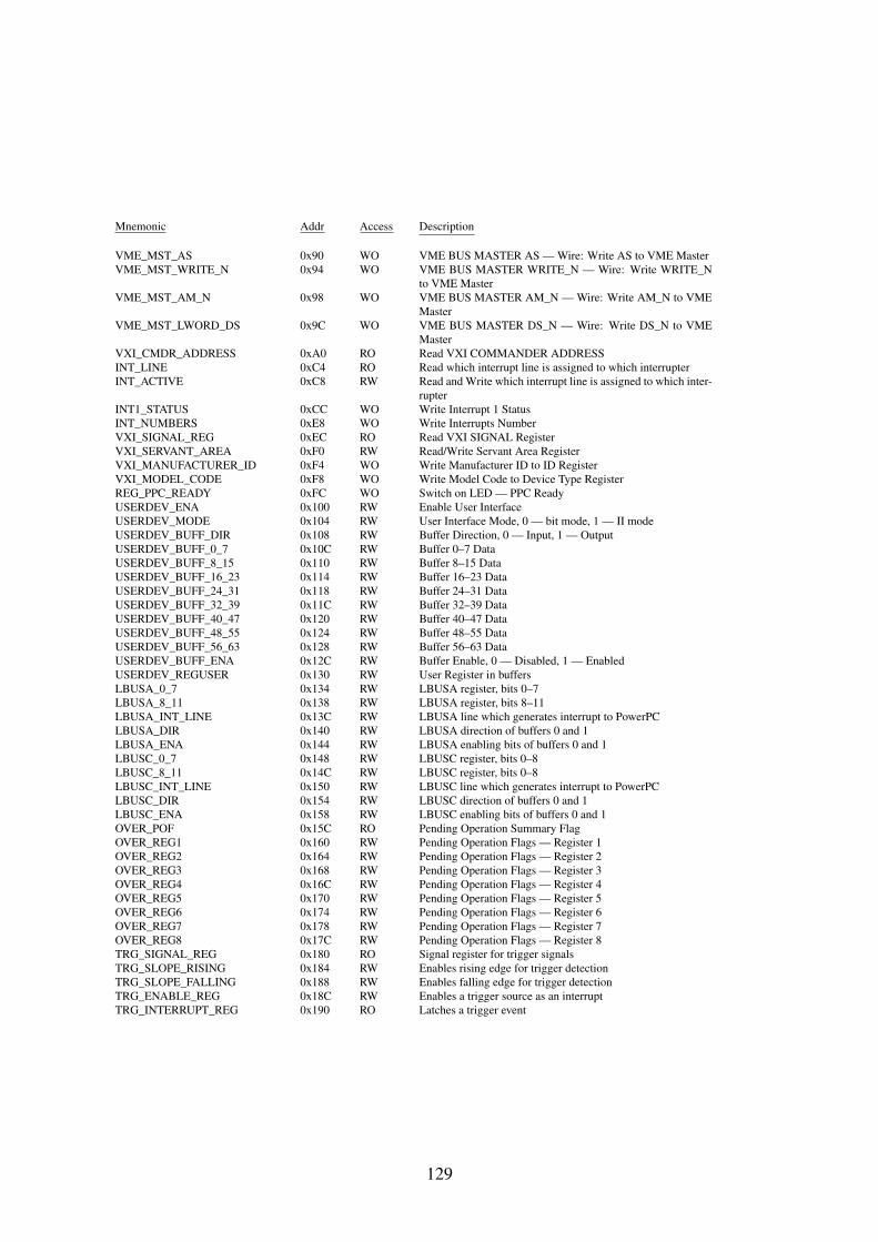
Mnemonic Addr Access Description
VME_MST_AS 0x90 WO VME BUS MASTER AS — Wire: Write AS to VME MasterVME_MST_WRITE_N 0x94 WO VME BUS MASTER WRITE_N — Wire: Write WRITE_N
to VME MasterVME_MST_AM_N 0x98 WO VME BUS MASTER AM_N — Wire: Write AM_N to VME
MasterVME_MST_LWORD_DS 0x9C WO VME BUS MASTER DS_N — Wire: Write DS_N to VME
MasterVXI_CMDR_ADDRESS 0xA0 RO Read VXI COMMANDER ADDRESSINT_LINE 0xC4 RO Read which interrupt line is assigned to which interrupterINT_ACTIVE 0xC8 RW Read and Write which interrupt line is assigned to which inter-
rupterINT1_STATUS 0xCC WO Write Interrupt 1 StatusINT_NUMBERS 0xE8 WO Write Interrupts NumberVXI_SIGNAL_REG 0xEC RO Read VXI SIGNAL RegisterVXI_SERVANT_AREA 0xF0 RW Read/Write Servant Area RegisterVXI_MANUFACTURER_ID 0xF4 WO Write Manufacturer ID to ID RegisterVXI_MODEL_CODE 0xF8 WO Write Model Code to Device Type RegisterREG_PPC_READY 0xFC WO Switch on LED — PPC ReadyUSERDEV_ENA 0x100 RW Enable User InterfaceUSERDEV_MODE 0x104 RW User Interface Mode, 0 — bit mode, 1 — II modeUSERDEV_BUFF_DIR 0x108 RW Buffer Direction, 0 — Input, 1 — OutputUSERDEV_BUFF_0_7 0x10C RW Buffer 0–7 DataUSERDEV_BUFF_8_15 0x110 RW Buffer 8–15 DataUSERDEV_BUFF_16_23 0x114 RW Buffer 16–23 DataUSERDEV_BUFF_24_31 0x118 RW Buffer 24–31 DataUSERDEV_BUFF_32_39 0x11C RW Buffer 32–39 DataUSERDEV_BUFF_40_47 0x120 RW Buffer 40–47 DataUSERDEV_BUFF_48_55 0x124 RW Buffer 48–55 DataUSERDEV_BUFF_56_63 0x128 RW Buffer 56–63 DataUSERDEV_BUFF_ENA 0x12C RW Buffer Enable, 0 — Disabled, 1 — EnabledUSERDEV_REGUSER 0x130 RW User Register in buffersLBUSA_0_7 0x134 RW LBUSA register, bits 0–7LBUSA_8_11 0x138 RW LBUSA register, bits 8–11LBUSA_INT_LINE 0x13C RW LBUSA line which generates interrupt to PowerPCLBUSA_DIR 0x140 RW LBUSA direction of buffers 0 and 1LBUSA_ENA 0x144 RW LBUSA enabling bits of buffers 0 and 1LBUSC_0_7 0x148 RW LBUSC register, bits 0–8LBUSC_8_11 0x14C RW LBUSC register, bits 0–8LBUSC_INT_LINE 0x150 RW LBUSC line which generates interrupt to PowerPCLBUSC_DIR 0x154 RW LBUSC direction of buffers 0 and 1LBUSC_ENA 0x158 RW LBUSC enabling bits of buffers 0 and 1OVER_POF 0x15C RO Pending Operation Summary FlagOVER_REG1 0x160 RW Pending Operation Flags — Register 1OVER_REG2 0x164 RW Pending Operation Flags — Register 2OVER_REG3 0x168 RW Pending Operation Flags — Register 3OVER_REG4 0x16C RW Pending Operation Flags — Register 4OVER_REG5 0x170 RW Pending Operation Flags — Register 5OVER_REG6 0x174 RW Pending Operation Flags — Register 6OVER_REG7 0x178 RW Pending Operation Flags — Register 7OVER_REG8 0x17C RW Pending Operation Flags — Register 8TRG_SIGNAL_REG 0x180 RO Signal register for trigger signalsTRG_SLOPE_RISING 0x184 RW Enables rising edge for trigger detectionTRG_SLOPE_FALLING 0x188 RW Enables falling edge for trigger detectionTRG_ENABLE_REG 0x18C RW Enables a trigger source as an interruptTRG_INTERRUPT_REG 0x190 RO Latches a trigger event
129

D.4 Configuration Options of VXI-IC
The configuration options of VXI-IC can be set up in two ways. First one is a configurationswitch on the VXI-IC board. The second one is tool.cfg configuration file loaded duringbooting process of the VXI-IC.
D.4.1 Configuration Switch
The configuration switch is used to set up the logical address of the VXI-IC on VME bus. Thisconfiguration switch is obligatory in the VXI standard. Figure D.1 presents how the eight bitsof the JP8 switch correspond to the A16 address on the VXI bus.
Figure D.1: JP8 — Logical Address Switch
The A16 VME address bits from A6 to A13 are compared in VXI-IC with the JP8 switch.The address bits A14 and A15 are always set to one by the VME master. Address bits from A1to A5 are used to address the 16-bit configuration and communication registers in VXI-IC.
D.4.2 Configuration file tool.cfg
The tool.cfg configuration file contains several parameters which are used to initiate theVXI-IC state during booting process. An example of the tool.cfg file looks as follows:
SCPI:SIMDSP.scpManufacturerID:3840ModelCode:1234IDN:VXI-MBT, KOPREK, V12, 34DeviceInterface:1DeviceMode:1DeviceEnable:0x4DeviceDir:0x0VXIAddrSpace:0VXIReqMem:5
130
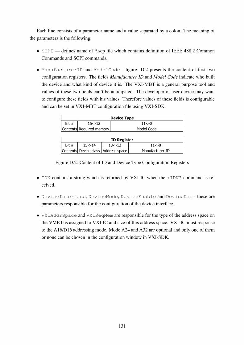
Each line consists of a parameter name and a value separated by a colon. The meaning ofthe parameters is the following:
• SCPI — defines name of *.scp file which contains definition of IEEE 488.2 CommonCommands and SCPI commands,
• ManufacturerID and ModelCode - figure D.2 presents the content of first twoconfiguration registers. The fields Manufacturer ID and Model Code indicate who builtthe device and what kind of device it is. The VXI-MBT is a general purpose tool andvalues of these two fields can’t be anticipated. The developer of user device may wantto configure these fields with his values. Therefore values of these fields is configurableand can be set in VXI-MBT configuration file using VXI-SDK.
Bit #
Contents
15<-14
Device class
13<-12
Address space
11<-0
Manufacturer ID
ID Register
Bit #
Contents
15<-12
Required memory
11<-0
Model Code
Device Type
Figure D.2: Content of ID and Device Type Configuration Registers
• IDN contains a string which is returned by VXI-IC when the *IDN? command is re-ceived.
• DeviceInterface, DeviceMode, DeviceEnable and DeviceDir - these areparameters responsible for the configuration of the device interface.
• VXIAddrSpace and VXIReqMem are responsible for the type of the address space onthe VME bus assigned to VXI-IC and size of this address space. VXI-IC must responseto the A16/D16 addressing mode. Mode A24 and A32 are optional and only one of themor none can be chosen in the configuration window in VXI-SDK.
131

D.5 VXI-IC Connectors
There are two connectors J8 and P8 for interfacing the user device. There are also other con-nectors: LED_P1 — for the VXI LEDs on the front panel, P9 — for the user LEDS, and P3 —for the serial port also on the front panel.
D.5.1 The User LEDs and the Front Panel Connectors
Figure D.3 presents pinout of the following connectors:
VXI LEDs connector is used to connect the LEDs mounted on the front panel of a VXImodule. Two of them are obligatory in the VXI standard: Ready and Failed. These LEDsreflect the state of bits with the same name in the Status Register. The access from the VXIbus to VXI-IC is indicated by the blinking diode Access. The diode SYSFAIL reflects a state ofthe SYSFAIL* line on the VXI bus.
1 2
3 4
5 6
1 2
3 4
5 6
7 8
1
2
3
GND
N.C.
Ready
Access
Failed
SYSFAIL
GND
GND
GND
USR_LED1
GND
GND
RxD
TxD
USR_LED2
USR_LED3
USR_LED4
LED_P1 — VXI LEDs P9 — User LEDs P3 — RS-232
Figure D.3: User LEDs and Front Panel Connectors Pinout
RS-232 port is used for debugging purposes. The developer may use it for interaction withthe PowerPC in VXI-IC. The manual of the RS-232 usage is in appendix D.6. The RS-232socket can be optionally mounted on the front panel of the VXI module.
User LEDs are general purpose diodes which can indicate any state of the user device orthe device driver. The state of these LEDs can be read and set from the device driver routinesusing the following C functions:void setUserLED(unsigned short ledNb, unsigned short ledState)—where first argument is LED number. The second argument is LED state where value 1 meansLED is on.unsigned short getUserLED(unsigned short ledNb) — this function returnsstate of the LED number ledNb.
D.5.2 Power Connector
The power connector provides 7 different voltages to the user device which are available onthe VXI backplane. Figure D.4 presents pinout of the connector.
132

1 2
3 4
5 6
7 8
9 10
11 12
13 14
GND
GND
GND
GND
GND
GND
GND
-5.2V
-2V
-24V
+24V
+5V
-12V
+12V
Figure D.4: Pinout of Power Connector
D.5.3 User Device Connector
The device interface connector can work in two modes: general purpose I/O mode and localbus mode. Depending on the mode, some of the pins play different role in the communicationwith the user device. Some pins are pre-defined and are constant regardless of the mode.
Convention of the GPIO pins naming is as follows:B<buff>_U<pin>_<direction> where:
• buff — buffer number from 0 to 7,
• pin — pin number from 0 to 61 formatted as two digit number,
• direction — predefined direction of the pin, possible values:IN — only input,OUT — only output,IO — input or output, defined by the user.
The meaning of pre-defined pins is as follows:
• power lines: +5V , +/− 12V ,
• GND — ground pins,
• VXI_TTLTRG0..7 — trigger lines, which are wired directly from the VXI backplane,
• VXI_ECLTRG0..1 — trigger lines also wired from the VXI backplane,
• VXI_CLK10 — 10 MHz clock wired from the VXI backplane,
• VXI_SERA, VXI_SERB — two lines for serial communication wired from the VXIbackplane,
• DEV_INT — interrupt line from the user device, which is connected in the FPGA tothe interrupt vector component,
133

• DEV_PON — Power ON pin connected to the message execution control component inthe FPGA,
• N.C. — not connected pin.
Configuration of the GPIO pins can be read from the device driver. The buffers enable/disablestate can be checked in the FPGA_USERDEV_BUFF_ENAworking register. The particular bitsof the register correspond to the particular buffers. The least significant bit is the buffer num-ber 0 and the most significant bit is the buffer 7. The value 0 means that a buffer is disabledand 1 — enabled. In a similar way, the buffers direction can be checked by reading value ofthe FPGA_USERDEV_BUFF_DIR working register, where value 1 means that the buffer isconfigured as an input, and value 0 — an output.
The state of the buffers can also be read from the control software using SCPI commandsas follow:
• :INSTrument:INTerface:BUFFer:DIRection? — this query reads theFPGA_USERDEV_BUFF_ENA working register, the meaning is the same as describedin the previous paragraph,
• :INSTrument:INTerface:BUFFer:ENABle? — this query reads theFPGA_USERDEV_BUFF_DIR working register, the meaning is the same as describedin the previous paragraph.
134

D.5.3.1 General Purpose I/O Mode
Table D.1: User Device Connector Pin Assignments in the GPIO Mode
Pin Number Row A Row B Row C1 B0_U00_IO VXI_TTLTRG0 B1_U08_IO2 B0_U01_IO VXI_TTLTRG1 B1_U09_IO3 B0_U02_IO VXI_TTLTRG2 B1_U10_IO4 B0_U03_IO N.C. B1_U11_IO5 B0_U04_IO B3_U24_IO B1_U12_IO6 B0_U05_IO B3_U25_IO B1_U13_IO7 B0_U06_IO B3_U26_IO B1_U14_IO8 B0_U07_IO B3_U27_IO B1_U15_IO9 GND B3_U28_IO GND10 VXI_CLK10 B3_U29_IO N.C.11 GND B3_U30_IO VXI_SERB12 DEV_INT B3_U31_IO VXI_SERA13 DEV_PON VXI_TTLTRG3 B4_U32_IO14 DEV_OPC* VXI_TTLTRG4 B7_U61_IN15 GND VXI_TTLTRG5 B6_U55_IO16 N.C. B7_U56_IN B6_U54_IO17 GND B7_U57_IN B6_U53_IO18 N.C. B7_U58_IN B6_U52_IO19 GND B7_U59_IN B6_U51_IO20 VXI_ECLTRG1 GND B6_U50_IO21 VXI_ECLTRG0 VXI_TTLTRG6 B6_U49_IO22 N.C. VXI_TTLTRG7 B6_U48_IO23 B7_U60_IN GND B5_U47_IO24 B4_U39_IO B2_U16_IO B5_U46_IO25 B4_U38_IO B2_U17_IO B5_U45_IO26 B4_U37_IO B2_U18_IO B5_U44_IO27 B4_U36_IO B2_U19_IO B5_U43_IO28 B4_U35_IO B2_U20_IO B5_U42_IO29 B4_U34_IO B2_U21_IO B5_U41_IO30 B4_U33_IO B2_U22_IO B5_U40_IO31 VXI_VDC-12V B2_U23_IO VXI_VDC+12V32 VXI_VDC+5V VXI_VDC+5V VXI_VDC+5V
There are C functions which enable access to the user lines state from the device driver:
• getUserDevBit(bitNumber) — This function reads a state of the bit numberbitNumber, which is in a range from 0 to 61. The returned value is 0 or 1.
• setUserDevBit(bitNumber,bitValue)— This function writes value bitValue(0 or 1) to the bit number bitNumber also in a range from 0 to 61.
There are also a SCPI command and a query which enable read and write of the user linestate from the control software. They are defined as follows:
135
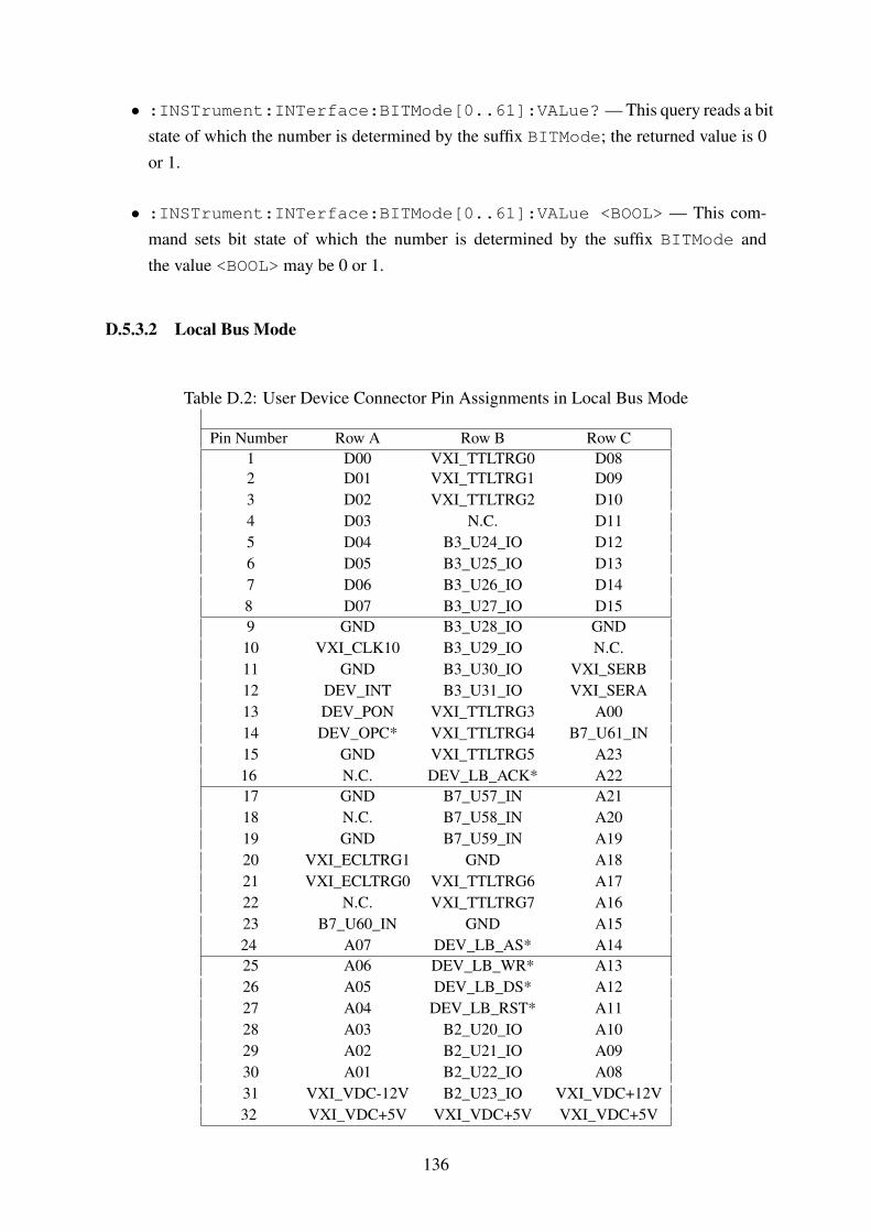
• :INSTrument:INTerface:BITMode[0..61]:VALue? — This query reads a bitstate of which the number is determined by the suffix BITMode; the returned value is 0or 1.
• :INSTrument:INTerface:BITMode[0..61]:VALue <BOOL> — This com-mand sets bit state of which the number is determined by the suffix BITMode andthe value <BOOL> may be 0 or 1.
D.5.3.2 Local Bus Mode
Table D.2: User Device Connector Pin Assignments in Local Bus Mode
Pin Number Row A Row B Row C1 D00 VXI_TTLTRG0 D082 D01 VXI_TTLTRG1 D093 D02 VXI_TTLTRG2 D104 D03 N.C. D115 D04 B3_U24_IO D126 D05 B3_U25_IO D137 D06 B3_U26_IO D148 D07 B3_U27_IO D159 GND B3_U28_IO GND10 VXI_CLK10 B3_U29_IO N.C.11 GND B3_U30_IO VXI_SERB12 DEV_INT B3_U31_IO VXI_SERA13 DEV_PON VXI_TTLTRG3 A0014 DEV_OPC* VXI_TTLTRG4 B7_U61_IN15 GND VXI_TTLTRG5 A2316 N.C. DEV_LB_ACK* A2217 GND B7_U57_IN A2118 N.C. B7_U58_IN A2019 GND B7_U59_IN A1920 VXI_ECLTRG1 GND A1821 VXI_ECLTRG0 VXI_TTLTRG6 A1722 N.C. VXI_TTLTRG7 A1623 B7_U60_IN GND A1524 A07 DEV_LB_AS* A1425 A06 DEV_LB_WR* A1326 A05 DEV_LB_DS* A1227 A04 DEV_LB_RST* A1128 A03 B2_U20_IO A1029 A02 B2_U21_IO A0930 A01 B2_U22_IO A0831 VXI_VDC-12V B2_U23_IO VXI_VDC+12V32 VXI_VDC+5V VXI_VDC+5V VXI_VDC+5V
136

The address space of the user device is mapped into the address space of the PowerPC localbus. The access to the user device registers from the device driver (in the C code) is donealike reads and writes to a memory. An address pointer to the base address of the user deviceaddress space is in the FPGA_USERDEV_BASE_ADDR constant. The address of a particularregister in the user device is calculated as a sum of the user device base address and the registeraddress. A list of the VXI-IC working registers, in appendix D.3, contains relative addresseswith respect to the base address of VXI-IC or the user device.
It is also possible to access the user device registers using SCPI messages, namely:
• :INSTrument:INTerface:LOCalbus:READ? <address>— This query readsvalue of the user device register of which the relative address is <address>.
• :INSTrument:INTerface:LOCalbus:WRITe <address>, <value> —This command writes signed integer value <value> to the register of which the relativeaddress is <address>.
D.5.3.3 The Handshake Protocol Timing
The figure D.5 presents a timing diagram of a read and write operation on the local bus be-tween VXI-IC and a user device. The VXI-IC is a master and drives lines DEV_LB_AS* (ad-dress strobe — address is valid), DEV_LB_ADDRESS (address lines), DEV_LB_DS* (datastrobe — data is valid in a write operation, VXI-IC ready for data in a read operation) andDEV_LB_WR* (read or write operation). The DEV_LB_DATA lines (data lines) are driven byVXI-IC in a write operation; the user device drives the data line in a read operation. The ac-knowledge line DEV_LB_ACK* is driven by the user device.
valid address valid address
valid data valid data
VXI-IC Clock
DEV_LB_AS*
DEV_LB_ADDRESS
DEV_LB_DS*
DEV_LB_DATA
DEV_LB_WR*
DEV_LB_ACK*
write operation read operation
Figure D.5: Timing Diagram of Reads and Writes from VXI-IC to the User Device
The user device works asynchronously with respect to the VXI-IC clock. The DEV_LB_ACK*
line can be asserted by the user device in any time but no longer than 20µs after the DEV_LB_AS*
line is asserted.
137
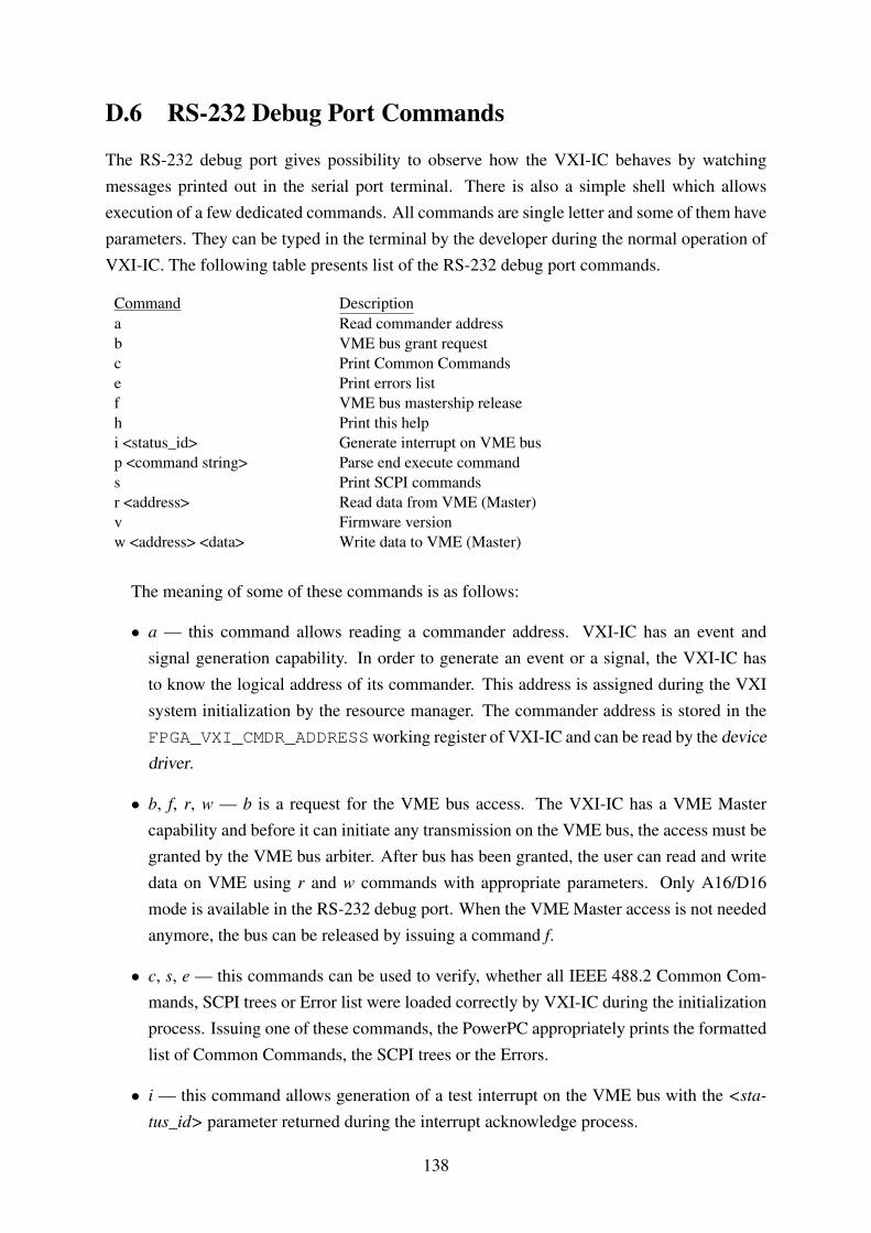
D.6 RS-232 Debug Port Commands
The RS-232 debug port gives possibility to observe how the VXI-IC behaves by watchingmessages printed out in the serial port terminal. There is also a simple shell which allowsexecution of a few dedicated commands. All commands are single letter and some of them haveparameters. They can be typed in the terminal by the developer during the normal operation ofVXI-IC. The following table presents list of the RS-232 debug port commands.
Command Descriptiona Read commander addressb VME bus grant requestc Print Common Commandse Print errors listf VME bus mastership releaseh Print this helpi <status_id> Generate interrupt on VME busp <command string> Parse end execute commands Print SCPI commandsr <address> Read data from VME (Master)v Firmware versionw <address> <data> Write data to VME (Master)
The meaning of some of these commands is as follows:
• a — this command allows reading a commander address. VXI-IC has an event andsignal generation capability. In order to generate an event or a signal, the VXI-IC hasto know the logical address of its commander. This address is assigned during the VXIsystem initialization by the resource manager. The commander address is stored in theFPGA_VXI_CMDR_ADDRESSworking register of VXI-IC and can be read by the devicedriver.
• b, f, r, w — b is a request for the VME bus access. The VXI-IC has a VME Mastercapability and before it can initiate any transmission on the VME bus, the access must begranted by the VME bus arbiter. After bus has been granted, the user can read and writedata on VME using r and w commands with appropriate parameters. Only A16/D16mode is available in the RS-232 debug port. When the VME Master access is not neededanymore, the bus can be released by issuing a command f.
• c, s, e — this commands can be used to verify, whether all IEEE 488.2 Common Com-mands, SCPI trees or Error list were loaded correctly by VXI-IC during the initializationprocess. Issuing one of these commands, the PowerPC appropriately prints the formattedlist of Common Commands, the SCPI trees or the Errors.
• i — this command allows generation of a test interrupt on the VME bus with the <sta-
tus_id> parameter returned during the interrupt acknowledge process.
138

• p — this command can be used to verify the functionality of a new SCPI command anda corresponding device driver routine. This is very useful option during the developmentprocess. When a new command is defined and loaded to VXI-IC, the developer can typethis command in the terminal and see its execution, without sending it through the VXIbus.
• v — this commands allows quick check of the firmware version in VXI-IC. The minorversion number is automatically incremented in VXI-SDK every time that the devicedeveloper compiles the device driver.
The debug messages can be printed out from device driver routines using the standard Cfunction printf.
139

D.7 VME master capability of VXI-IC
The VME master component is connected to the VME bus from one side and to the local busof the PowerPC on the other. From the processor point of view, it is implemented as a set ofregisters which are used by the PowerPC software to control the component. The meaningof the registers is not explained here because the following C functions give full access tothe component functionality:
• int vmeBusRequest(void);
void vmeBusRelease(void);
First of all, the VME bus access must be granted by the VME bus arbiter located inthe slot 0 of a VXI chassis. The function has no parameters and it returns 0, when the busis granted, and a positive value — when an error occurred. The bus can be released any-time and the vmeBusRelease function neither takes a parameter nor returns a value.
• int readVXIReg(unsigned short device, unsigned short reg,
unsigned long *data);
int writeVXIReg(unsigned short device, unsigned short reg,
unsigned long data);
When the bus is granted, the developer can use these functions to read and write registerof another VXI device in the system within the A16/D16 address space. In both cases,the first parameter is a logical address of the target VXI device, the second parameter isa register number. The absolute A16 address on the VME bus is calculated by the func-tion using values of these two parameters. The third parameter is a pointer to the returneddata for the read function. For the write function, the third parameter contains data to besent. The functions return 0 if the VME access was successful, and 1 if a bus erroroccurred.
• int writeVMEMaster(unsigned long address, unsigned long data,
unsigned int vmeAM, unsigned int vmeDS);
int readVMEMaster(unsigned long address, unsigned long *data,
unsigned int vmeAM, unsigned int vmeDS);
These two functions give possibility to get access to any address in any address space onthe VME bus. The first parameter is an absolute VME address in a given address space.The second address is a value to be sent for the write function and a pointer to a data to bereceived for the read function. The third parameter determines the Address Modifier onthe VME bus which corresponds to the address space such as A16 (value 0), A24 (value1) or A32 (value 3). The last parameter determines the data size on the VME bus and itcan be D16 (value 0) or D32 (value 1).
140

• unsigned long vxiReadCMDRAddress(void);
This last function is used to determine the commander logical address of a device. Thisfunction doesn’t access the VME bus, but it is important for the event and signal ge-neration mechanism. Before a signal/event can be sent to the commander using thewriteVXIReg function, the logical address of the commander must be known.
141

D.8 VME Interrupt Requester Manual
The VME interrupt requester can also be used directly from the device driver. According to theVXI specification, it is implemented as a Realease On Acknowledge (ROAK) version. Thereare two functions which can be used in the device driver:
• unsigned long vmeIntReq(unsigned short status);
This function is used to generate an interrupt on the VME bus. When the interrupt lineis asserted on the VME bus, the interrupt handler in the VXI-IC commander performsan interrupt acknowledge cycle. During the cycle, the status ID word is prompted fromthe VXI-IC interrupt requester and then, the status ID word is forwarded by the interrupthandler routine to the control software. The status ID word is 16 bits wide and its formatis presented in figure D.6.
status logical address
07815
Figure D.6: Format of status ID word
The logical address tells the interrupt handler routine which device has requested theservice. The status field says what kind of service has been requested.
• unsigned short vmeIntLine(void);
This function returns an interrupt line number which is assigned to the VXI-IC duringthe VXI chassis initialization.
142

D.9 Implemented Standard VXI Registers
Figure D.7 presents list of registers defined by the VXI standard. The gray registers are im-plemented in the VXI interface component of VXI-IC. The detailed description of registerscontent is in the VXI specification.
IDRegister
Device Type
A24/A32 Offset Register
0x00
0x02
0x04
0x06
0x08
0x0A
Data High0x0C
Data Low0x0E
A24 Pointer High0x10
A24 Pointer Low0x12
A32 Pointer High0x14
A32 Pointer Low0x16
Read
Logical Address
Status Register Control Register
Protocol Register Signal Register
Response Register Data Extended
Write
VXI Reserved
A16
Configuration Registers
Communication Registers
Shared Memory Protocol
Registers
Figure D.7: VXI Configuration & Communication Registers
143
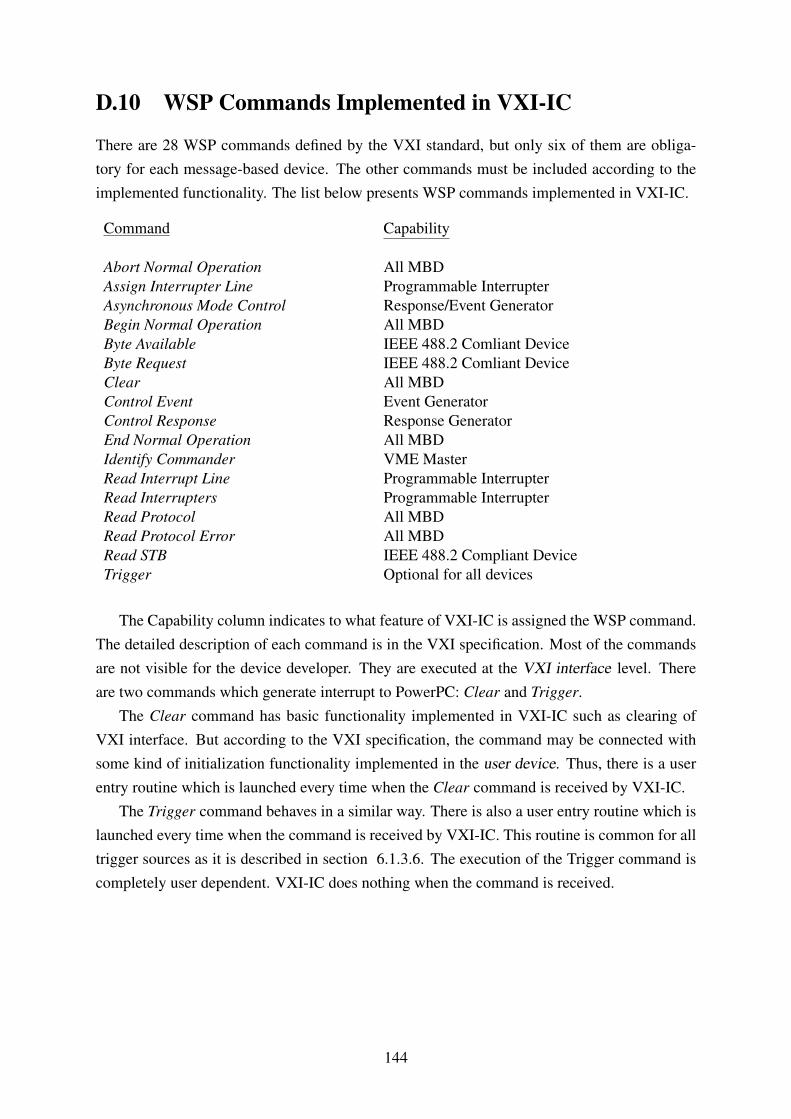
D.10 WSP Commands Implemented in VXI-IC
There are 28 WSP commands defined by the VXI standard, but only six of them are obliga-tory for each message-based device. The other commands must be included according to theimplemented functionality. The list below presents WSP commands implemented in VXI-IC.
Command Capability
Abort Normal Operation All MBDAssign Interrupter Line Programmable InterrupterAsynchronous Mode Control Response/Event GeneratorBegin Normal Operation All MBDByte Available IEEE 488.2 Comliant DeviceByte Request IEEE 488.2 Comliant DeviceClear All MBDControl Event Event GeneratorControl Response Response GeneratorEnd Normal Operation All MBDIdentify Commander VME MasterRead Interrupt Line Programmable InterrupterRead Interrupters Programmable InterrupterRead Protocol All MBDRead Protocol Error All MBDRead STB IEEE 488.2 Compliant DeviceTrigger Optional for all devices
The Capability column indicates to what feature of VXI-IC is assigned the WSP command.The detailed description of each command is in the VXI specification. Most of the commandsare not visible for the device developer. They are executed at the VXI interface level. Thereare two commands which generate interrupt to PowerPC: Clear and Trigger.
The Clear command has basic functionality implemented in VXI-IC such as clearing ofVXI interface. But according to the VXI specification, the command may be connected withsome kind of initialization functionality implemented in the user device. Thus, there is a userentry routine which is launched every time when the Clear command is received by VXI-IC.
The Trigger command behaves in a similar way. There is also a user entry routine which islaunched every time when the command is received by VXI-IC. This routine is common for alltrigger sources as it is described in section 6.1.3.6. The execution of the Trigger command iscompletely user dependent. VXI-IC does nothing when the command is received.
144

D.11 VXI-IC Status Registers
D.11.1 IEEE 488.2 Compliant Status Registers
The status registers in VXI-IC are implemented according to the IEEE 488.2 standard and SCPIspecification. Both define some amount of status registers for the device state reporting. FigureD.8 presents obligatory status registers required by the IEEE 488.2 standard.
RQS
6
MSSESB MAV 3 2 1 07
SERVICE REQUEST
GENERATION
5 4 3 2 07 1
&&
&&
&&
&
7 6 5 4 3 2 1 0
7 6 5 4 3 2 1 0
&&
&&
&&
&&
Status Byte Register
read by *STB?
read by Serial Poll
Queue
Not-Empty
Output Queue
Service Request
Enble Register
*SRE<NRf>
*SRE?
Standard
Event Status Register
*ESR?
Standard
Event Status
Enable Register
*ESE<NRf>
*ESE?
Logi
cal O
R
Logi
cal O
R
Pow
er O
n
Use
r R
eque
st
Com
man
d E
rror
Exe
cutio
n E
rror
Dev
ice
Dep
ende
nt E
rror
Que
rry
Err
or
Req
uest
Con
trol
Ope
ratio
n C
ompl
ete
Figure D.8: Status Registers defined by IEEE 488.2
There are some comments in the figure which include Common Commands names. Thesecommands correspond to the particular registers and are used for configuration and readoutof them. Nine of the thirteen obligatory Common Commands operate on the status registers.The details how these commands act on the status registers are described in the IEEE 488.2specification, section 11. All registers are implemented in VHDL and the content of theseregisters is mapped into the address space of the PowerPC local bus. All mnemonics related tothese registers are listed in appendix D.3.
D.11.2 SCPI Specification Status Registers
The SCPI specification defines status registers which are related to the device functions. Fig-ure D.9 presents registers defined by the SCPI specification in addition to the status registersdefined by the IEEE 488.2 standard. These registers are also implemented in VXI-IC.
145
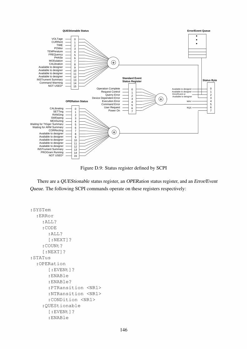
0123456789101112131415
VOLTageCURRent
TIMEPOWer
TEMPeratureFREQuency
PHASeMODulationCALibration
Available to designerAvailable to designerAvailable to designerAvailable to designer
INSTrument SummaryCommand Warming
NOT USED*
+
0123456789101112131415
CALibratingSETTing
RANGingSWEeping
MEASuringWaiting for TIGger Summary
Waiting for ARM SummaryCORRecting
Available to designerAvailable to designerAvailable to designerAvailable to designerAvailable to designer
INSTrument SummaryPROGram Running
NOT USED*
+
QUEStionable Status
OPERation Status
01234567
Operation CompleteRequest Control
Querry ErrorDevice Dependent Error
Execution ErrorCommand Error
User RequestPower On
++
Standard Event Status Register
01234567
••
•
Error/Event Queue
Available to designerAvailable to designerError/Event or Available to deisgner
MAV
RQS
Status Byte
Figure D.9: Status register defined by SCPI
There are a QUEStionable status register, an OPERation status register, and an Error/EventQueue. The following SCPI commands operate on these registers respectively:
:SYSTem:ERRor
:ALL?:CODE
:ALL?[:NEXT]?
:COUNt?[:NEXT]?
:STATus:OPERation
[:EVENt]?:ENABle:ENABle?:PTRansition <NR1>:NTRansition <NR1>:CONDition <NR1>
:QUEStionable[:EVENt]?:ENABle
146

:ENABle?:PTRansition <NR1>:NTRansition <NR1>:CONDition <NR1>
:PRESet
The :SYSTem:ERRor subtree is used to operate on the Error/Event Queue. The details ofeach command is in the SCPI specification. The content of the QUEStionable and OPERationregisters can be accessed from the device driver because they are available on the PowerPC localbus under the following mnemonics: OPER_VALUE_ADDRESS and QUES_VALUE_ADDRESS.Other mnemonics related to these register are listed in appendix D.3.
147

D.12 VXI-IC LBUS Implementation
The VXI-IC has implemented a local bus connected to adjacent VXI modules on both sides.The 12 lines of LBUSA and LBUSC are divided into two buffers. The buffers are bidirectional,each of the buffers can be set to a specific direction. Each buffer can be enabled and disabledat any time. There is also additional feature which allows choosing the line of LBUS whichcan generate an interrupt to PowerPC with either a rising or falling edge. This feature is usefulwhen the developer wants to implement a communication protocol. If the VXI-IC works as aslave on the particular LBUS, then it doesn’t need to check continuously in a loop what is theline state. For example, the developer can choose which line is responsible for transmissioninitialization and the level change on this line will generate an interrupt to PowerPC. The in-terrupt handler in the processor calls a user entry routine where the developer can implementa custom communication protocol. Figure D.10 presents physical connection of FPGA andLBUS buffers.
FPGA
0
.
.
7
8
.
11
8
4
8
4
0
.
.
7
8
.
11
8
4
8
4
ENA
DIR
ENA
DIR
ENA
DIR
ENA
DIR
LBUSA LBUSC
Slot NSlot N-1 Slot N+1
VXI-ICB0
B1
B0
B1
Figure D.10: Implementation of LBUS
Figure D.11 contains a list of working registers which are responsible for the LBUSA andLBUSC functionality. Each register can be read and written.
7 6 5 4 3 2 1 0
11 10 9 8
Sl Int Line
B1 B0
B1 B0
7 6 5 4 3 2 1 0
11 10 9 8
Sl Int Line
B1 B0
B1 B0
LBUSA_0_7
LBUSA_8_11
LBUSA_INT_LINE
LBUSA_DIR
LBUSA_ENA
LBUSC_0_7
LBUSC_8_11
LBUSC_INT_LINE
LBUSC_DIR
LBUSC_ENA
Figure D.11: Working registers of LBUS
The registers LBUSx_x_x are used to latch the state of the LBUSx line. Depending onthe buffer direction, the LBUSx_x_x are read only or write only. The LBUSx_DIR register is
148
responsible for determination of the B0 and B1 direction. Value 0 means that the buffer worksas an input, for value 1 the buffer works as an output. Setting to 1 the bits B0 or B1 of registerLBUSx_ENA enables the buffers B0 and B1. The bits from 0 to 3 of the LBUSx_INT_LINEregister determine which line generates an interrupt to PowerPC. The value of this field can befrom 0 to 11 which corresponds to LBUSx lines. By default, the register value is set to 15 whichmeans, no line generates an interrupt. The bit 4 of the LBUSx_INT_LINE register determineswhich slope generates the interrupt - value 0 corresponds to the rising edge and value 1 to thefalling edge.
All registers can be accessed from the device driver routines using the register mnemonics.Based on these registers and LBUS interrupts to PowerPC, the developer is free to program anycustom protocol which can be used for communication with other VXI modules.
149
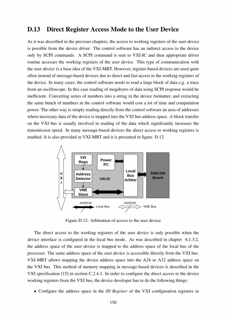
D.13 Direct Register Access Mode to the User Device
As it was described in the previous chapters, the access to working registers of the user deviceis possible from the device driver. The control software has an indirect access to the deviceonly by SCPI commands. A SCPI command is sent to VXI-IC and then appropriate driverroutine accesses the working registers of the user device. This type of communication withthe user device is a base idea of the VXI-MBT. However, register-based devices are used quiteoften instead of message-based devices due to direct and fast access to the working registers ofthe device. In many cases, the control software needs to read a large block of data e.g. a tracefrom an oscilloscope. In this case reading of megabytes of data using SCPI response would beinefficient. Converting series of numbers into a string in the device formatter, and extractingthe same bunch of numbers in the control software would cost a lot of time and computationpower. The other way is simply reading directly from the control software an area of addresseswhere necessary data of the device is mapped into the VXI bus address space. A block transferon the VXI bus is usually involved in reading of the data which significantly increases thetransmission speed. In many message-based devices the direct access to working registers isenabled. It is also provided in VXI-MBT and it is presented in figure D.12.
VXI
VMESlave
VXIRegs
LocalBus
Arbiter
PowerPC
SIMCONBoard
AddressDetector
Local Bus VME Bus
VXI-IC
A24/D16 A32/D32
Figure D.12: Arbitration of access to the user device
The direct access to the working registers of the user device is only possible when thedevice interface is configured in the local bus mode. As was described in chapter 6.1.3.2,the address space of the user device is mapped to the address space of the local bus of theprocessor. The same address space of the user device is accessible directly from the VXI bus.VXI-MBT allows mapping the device address space into the A24 or A32 address space onthe VXI bus. This method of memory mapping in message-based devices is described in theVXI specification [15] in section C.2.4.3. In order to configure the direct access to the deviceworking registers from the VXI bus, the device developer has to do the following things:
• Configure the address space in the ID Register of the VXI configuration registers in
150

VXI-IC to A16/A24 or A16/A32 mode. The configuration is done in VXI-SDK.
• Configure the required memory amount in the Device Type register of the VXI configu-ration registers in VXI-IC. The VXI controller assigns an address space large enough tocover the address space of the device working registers, see section 6.1.3.8. This featureis also configured in VXI-SDK.
During initialization process of the VXI system, the controller reads the configuration reg-isters of the devices to check if there is a device in the system which needs address space inA24 or A32 address space. If there is such a device, the controller writes to the Offset Register
a base address for the particular device. More details one can find in the VXI specification,section C.2.1.1.2. The base address assigned to the VXI-IC on the VXI bus corresponds to theuser device register at zero address. Since the local bus of the user device has 24 address linesand 16 data lines, only A24/D16 or A32/D32 access mode on VME is allowed. As presented infigure D.12, the VME Slave component is a slave with regard to the VXI bus communication,but it is a master on the local bus. It means that there are two masters: the processor and theVME slave which can simultaneously initiate transmission on the local bus to the user device.In order to avoid a conflict on the local bus, the Local Bus Arbiter was implemented.
151

D.14 Sequential and Overlapped Mode of Commands Exe-cution
The IEEE 488.2 defines two modes of command execution: sequential and overlapped mode.In the sequential mode, the next command can be executed when the first one has finished. Inoverlapped mode, the next command can be executed while the previous one is still in progress.The situation gets complicated when an execution of the given command depends on comple-tion of another one issued a while ago. In this case there is a pending-operation flag defined bythe standard which is used together with the Common Commands *OPC, *OPC? and *WAI tosynchronize the operation of a device and a controller, see also appendix D.1.
Because all of the Common Commands and SCPI commands implemented in VXI-IC areexecuted sequentially, there is no need to implement this mechanism for VXI-IC. Nevertheless,the developer may want to implement overlapped commands for his device. For this purposea dedicated line was designed in the device connector. The line is named DEV_OPC* andis connected to one of the bit in a dedicated OVER_REG1 register in VXI-IC. The negationmeans that the line is always zero even if the user device doesn’t use the line, i.e. there isno overlapped commands implemented in the user device. If the device developer wants toimplement overlapped commands, he must take care of setting this line to one in the userdevice when the overlapped command is executed.
0 OVER_POF
OR
OVER_REG1 OVER_REG2 ...OVER_REG3 OVER_REG80
DE
V_O
PC
*
0 31 0 31 0 31 0 31
... ... ... ...Set by Device Driver
Figure D.13: Configuration of Working Registers for Overlapped Mode of Command Execu-tion
The developer may also want to set a pending operation flag directly from the device driver.For that purpose a set of OVER_REGx registers was implemented in VXI-IC as it is presentedin figure D.13. There is 8 registers 32-bit each. The bit 0 of the first register is connectedto the DEV_OPC* line. The other bits are read and set from the device driver. Each bit maycorrespond to one overlapped command. The bits assignment is up to the developer. All bitsfrom the eight registers are ored and connected to one global bit in the register OVER_POFwhich corresponds to the pending-operation flag defined by the IEEE 488.2 standard.
152

D.15 Formatting Routines
The formatting routines are used by the device developer to format the response string fordevice-specific SCPI queries according to the IEEE 488.2 syntax. There is a set of formattingroutines which accept native data types and generate response strings put into the output queue.All formats of the string generated by the formatter routines are described in the IEEE 488.2standard. The formatting routines are defined as follows:
• unsigned long formatCHARACTER(unsigned char *string);
Tthis function puts into the output queue one of the allowed respone CHARACTERs.The CHARACTER string is a parameter of the function.
• unsigned long formatNR1(double value);
unsigned long formatNR2(double value);
unsigned long formatNR3(double value);
The formatNRx functions convert a variable value of double type into a string represent-ing a number in format NR1, 2, or 3 according to the ANSI X3.42-1975 standard [69],
• unsigned long formatBinary(unsigned int);
unsigned long formatOctal(unsigned int);
unsigned long formatHexadecimal(unsigned int);
A number can be returned in non-decimal format such as a binary, octal or hexadeci-mal number. Passing numbers in one of these formats may later simplify parsing of theresponse string in the control software,
• unsigned long formatString(char *string, unsigned short quote);
The string of data to be sent is formatted into string enclosed in single quotes (paramquote is 0) or in double quotes (param quote is 1),
• unsigned long formatABPD(unsigned short *data,
unsigned short format);
This function puts into the output queue an arbitrary block program data as a byte se-quence in definite length format (param format is 0) or as an indefinite length format(param format is 1).
• unsigned long formatExpression(unsigned char *string);
This function puts into the output queue a string formatted by the driver routine. Thestring is taken as it is passed and the formatter only encloses it in parenthesis.
All these functions return 0 if the formatting operation has finished successfully, and theyreturn 1 when the output queue is full.
153
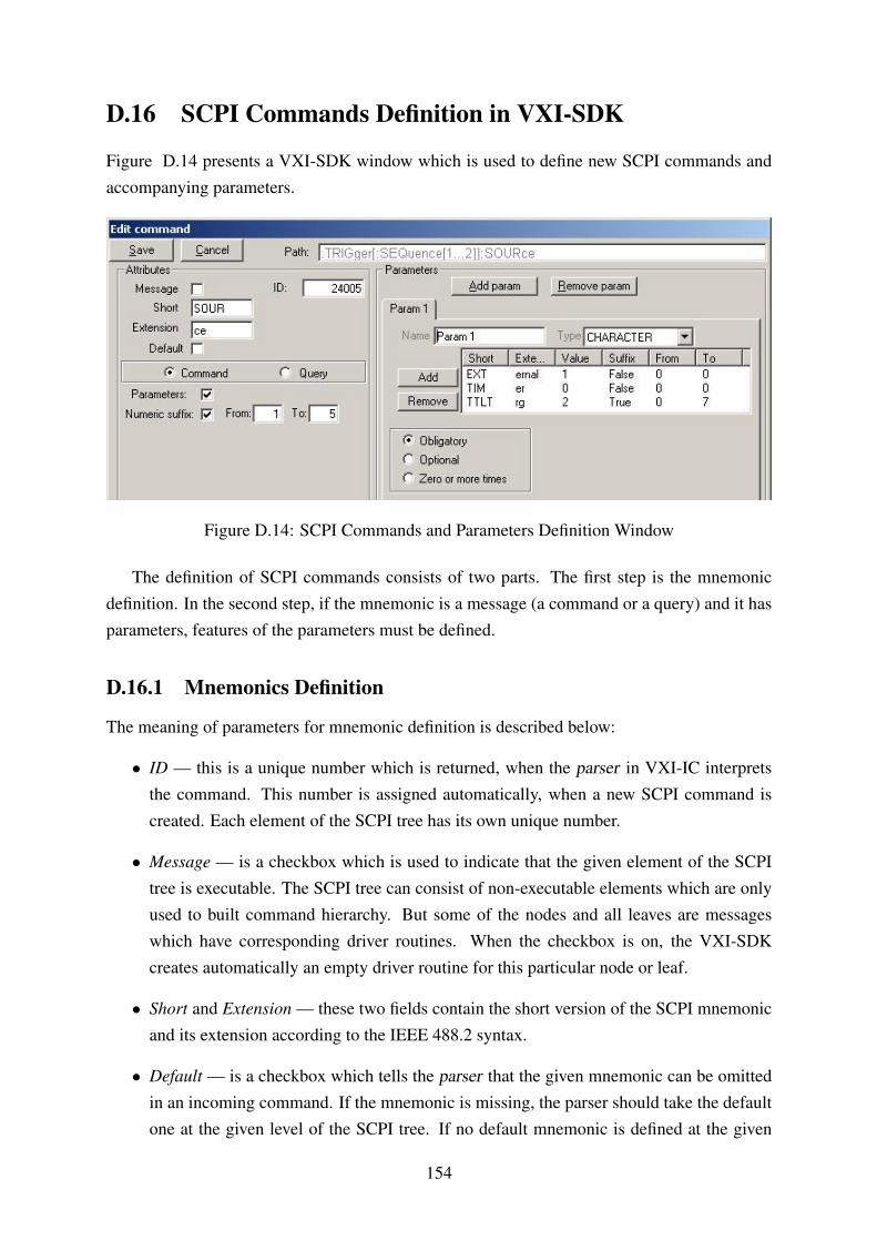
D.16 SCPI Commands Definition in VXI-SDK
Figure D.14 presents a VXI-SDK window which is used to define new SCPI commands andaccompanying parameters.
Figure D.14: SCPI Commands and Parameters Definition Window
The definition of SCPI commands consists of two parts. The first step is the mnemonicdefinition. In the second step, if the mnemonic is a message (a command or a query) and it hasparameters, features of the parameters must be defined.
D.16.1 Mnemonics Definition
The meaning of parameters for mnemonic definition is described below:
• ID — this is a unique number which is returned, when the parser in VXI-IC interpretsthe command. This number is assigned automatically, when a new SCPI command iscreated. Each element of the SCPI tree has its own unique number.
• Message — is a checkbox which is used to indicate that the given element of the SCPItree is executable. The SCPI tree can consist of non-executable elements which are onlyused to built command hierarchy. But some of the nodes and all leaves are messageswhich have corresponding driver routines. When the checkbox is on, the VXI-SDKcreates automatically an empty driver routine for this particular node or leaf.
• Short and Extension — these two fields contain the short version of the SCPI mnemonicand its extension according to the IEEE 488.2 syntax.
• Default — is a checkbox which tells the parser that the given mnemonic can be omittedin an incoming command. If the mnemonic is missing, the parser should take the defaultone at the given level of the SCPI tree. If no default mnemonic is defined at the given
154

level, the parser returns an error. The default mnemonic is emphasized in square bracketsin the SCPI tree.
• Command or Query — these options are used to determine if the message is a commandor a query. If the message is simultaneously a command and a query, it must be definedseparately in two steps, because the command may have different parameters than thecorresponding query. The query mnemonic has a question mark following the mnemonic.
• Parameters — the field is checked when the SCPI message has at least one parameter.Then, a frame with the parameter list appears on the right side of the window.
• Numeric suffix — this checkbox says that the given mnemonic has a suffix. When thefield is checked, the developer can specify range of the suffixes in two additional numericfields in the window.
D.16.2 Parameters Definition
When Parameters checkbox is selected, the list of parameters appears on the right side ofthe Command Definition window. Each parameter appears on a separate tab. The name of theparameter can be specified in the Name field and it is displayed on the tab. There are eight typesof parameters which can be defined: character, NR1, NR2, NR3, string, boolean, arbitrary blockprogram data (ABPD) and expression. Depends on the parameter type, different parameteroptions appear in the frame below the name. All parameters are implemented according to theIEEE 488.2 standard and SCPI specification.
155

D.17 Built-in C Routines for Specific SCPI Driver
There is a number of C routines precompiled in the VXI-IC firmware which can be used by thedevice developer in the device driver or in the user entry routines.
All of the routines were described in the previous chapters and appendices. The list in-cluded below presents in a concise form the implemented routines:
User LEDs operation:
void setUserLED(unsigned short ledNb, unsigned short ledState);unsigned short getUserLED(unsigned short ledNb);
Device interface operation:
unsigned short getUserDevBit(unsigned short bitNumber);unsigned long setUserDevBit(unsigned short bitNumber, unsigned short bitValue);unsigned short getUserBuffer(unsigned short buffNb);unsigned long setUserBuffer(unsigned short buffNb, unsigned short value);unsigned long readDevReg(unsigned long address, unsigned int *value);unsigned long writeDevReg(unsigned long address, unsigned int value);
VME Master operation and event and signal generation:
int vmeBusRequest(void);void vmeBusRelease(void);int readVXIReg(unsigned short device, unsigned short reg,
unsigned long *data);int writeVXIReg(unsigned short device, unsigned short reg,
unsigned long data);unsigned long writeVMEMaster(unsigned long address, unsigned long data,
unsigned int vmeAM, unsigned int vmeDS);unsigned long readVMEMaster(unsigned long address, unsigned long *data,
unsigned int vmeAM, unsigned int vmeDS);unsigned long vxiReadCMDRAddress(void);
VME Interrupts operation:
unsigned long vmeIntReq(unsigned short status);unsigned short vmeIntLine(void);
Formatter routines:
unsigned long formatCHARACTER(unsigned char *string);unsigned long formatNR1(double value);unsigned long formatNR2(double value);unsigned long formatNR3(double value);unsigned long formatBinary(unsigned int);unsigned long formatOctal(unsigned int);unsigned long formatHexadecimal(unsigned int);unsigned long formatString(char *string, unsigned short quote);unsigned long formatABPD(unsigned short *data, unsigned short format);unsigned long formatExpression(unsigned char *string);
156

D.18 Trigger Detection Subsystem
There are 11 sources of triggers which can be detected by VXI-IC: eight TTLTRG signals, twoECLTRG signals and a WSP Trigger Common Command. All of them can be selected as asource for the trigger subsystem in VXI-IC. Each of these sources may generate an interruptto PowerPC. When the interrupt is generated, PowerPC launches a trigger interrupt handler
routine. Figure D.15 presents a set of registers which are used for the trigger sources.
10 9 8 7 6 5 4 3 2 1 0
TT
LTR
G7
TT
LTR
G6
TT
LTR
G5
TT
LTR
G4
TT
LTR
G3
TT
LTR
G2
TT
LTR
G1
TT
LTR
G0
EC
LTR
G0
EC
LTR
G1
WS
PT
RG
TRG_SIGNAL_REG
TRG_SLOPE_RISINGTRG_SLOPE_FALLING
Slope detector
10 9 8 7 6 5 4 3 2 1 0 TRG_ENABLE_REG
OR
To PowerPC Interrupt Vector
10 9 8 7 6 5 4 3 2 1 0 TRG_INTERRUPT_REG
Figure D.15: Trigger Detection Subsystem
All trigger sources are disabled by default. One can read the current state of an individ-ual line by reading the TRG_SIGNAL_REG register. The trigger line can generate an inter-rupt on a positive slope, on a negative slope, or on both. These options can be set in theTRG_SLOPE_RISING and TRG_SLOPE_FALLING registers. A value 1 in the particular bit ofthe register enables interrupt generation on one or both of the select slopes. There is no slopeselection for the WSP Trigger command, because the interrupt is generated every time whenthis command is detected by the WSP execution component. All trigger source are disabledby default. They can be enabled in the TRG_ENABLE_REG register. Each trigger line canbe enabled individually. The enabled trigger source is latched in the TRG_INTERRUPT_REG
register. The logical OR of the bits from this register is wired to the main interrupt vector ofthe PowerPC. When the interrupt is generated to the PowerPC, the trigger interrupt handler
routine is launched. The developer can program in this routine any scheme of trigger systemappropriate for his application.
157

D.19 Contents of the Attached CD-ROM
The attached CD-ROM contains the following items:
• Source code of VXI-SDK. This is a Microsoft Visual Studion 6.0 project. The code iswritten in Visual Basic 6.0 — folder VXISDK_VB.
• VXI-IC firmware. It is a Xilinx EDK Studio 8.2 project. It includes VHDL components,bootloader and VXI-IC driver — folder VXIIC_EDK.
• Schematics and PCB of VXI-IC. This is a project for Protel DXP 2000 —folder VXIIC_DXP.
• This thesis in pdf format — root folder.
158
Related Documents