pubs.acs.org/Macromolecules Published on Web 09/04/2009 r 2009 American Chemical Society 7924 Macromolecules 2009, 42, 7924–7929 DOI: 10.1021/ma901365c Fabrication of Poly(vinylidene fluoride-trifluoroethylene)/ Poly(3,4-ethylenedioxythiophene)-Polystyrene Sulfonate Composite Nanofibers via Electrospinning Osmarie Martı´nez, † Ariana G. Bravo, † and Nicholas J. Pinto* ,‡ † Department of Biology and ‡ Department of Physics and Electronics, University of Puerto Rico-Humacao, Humacao, PR 00791 Received June 25, 2009; Revised Manuscript Received August 14, 2009 ABSTRACT: Nanofibers of PVF 2 -TrFE/PEDOT-PSS were fabricated at room temperature using electrospinning with the thinnest fiber having a diameter of ∼15 nm. This process for generating PVF 2 -TrFE/PEDOT-PSS composite nanofibers is cheap, fast, and reliable. The presence of conducting PEDOT-PSS assisted in the fabrication of PVF 2 -TrFE nanofibers at low polymer concentrations in N,N,-dimethylformamide and energy dispersive X-ray spectroscopy confirmed the presence of PEDOT-PSS in the nanofibers. As a fiber mat, they were electrically conducting and used in the fabrication of a Schottky diode, and the diode parameters were calculated assuming the standard thermionic emission model of a Schottky junction. Being a composite, these nanofibers are promising candidates for use in a variety of applications that can take advantage of the ferroelectric and/or conducting properties of each individual component. In addition, the large aspect ratio and even larger surface to volume ratio of the fibers makes them ideal candidates in the fabrication of miniaturized, low power consumption devices, and supersensitive sensors. Introduction The electrically insulating polymer, poly(vinylidene fluoride) (-CF 2 -CH 2 -) (PVF 2 ) and some of its copolymers with tri- fluoroethylene (-CF 2 -CHF-) (TrFE) are known to exhibit ferroelectric behavior. 1-7 While PVF 2 can exist in several differ- ent forms, not all of which are polar, the copolymer poly- (vinylidene fluoride-trifluoroethylene), (-CF 2 -CH 2 -) n -(CF 2 - CHF-) m (PVF 2 -TrFE) is polar for TrFE content in the range 20-50% at room temperature 3 and consists of an all trans configuration as shown in Figure 1a. The bistable nature of the permanent electrical dipoles that point perpendicular to the polymer backbone are responsible for the observable macro- scopic polarization and has been put to use in nonvolatile organic memory devices. 8-11 Such information storage devices, where the basic storage element is the metal/ferroelectric poly- mer/metal capacitor, have been fabricated using low cost solu- tion processability usually via spin coating techniques that lead to thin film based devices and are two-dimensional (2D) in nature. More recently, ferroelectric polymers have also been employed as the gate dielectric in the fabrication of ferroelectric field effect transistors (FeFET), where the polarization of the ferroelectric via a gate voltage controls the charge transport across a semiconducting channel in intimate contact with the gate dielectric. 12-14 Conducting polymers, on the other hand, also form another class of technologically important organic materials whose ap- plications range from corrosion prevention of metals 15 to more complex uses in organic field effect transistors 16-18 and other optoelectronic devices. 19,20 Unique to conducting polymers is the concept of doping, where the conductivity of the polymer can be varied controllably and reversibly without degradation, by sev- eral orders of magnitude 21 from the insulating to the conducting state and vice versa, a feature not possible in traditional metals. While doped polyaniline has aroused wide scientific interest, the conducting polymer poly(3,4-ethylenedioxthiophene)-PEDOT is technologically more desirable and hence has been used in most polymer based electronic applications. One of the reasons is that PEDOT is very stable in the doped state with conducting proper- ties that remain unchanged with time under ambient environ- mental conditions. 22 Using a water-soluble polyelectrolyte (poly- styrene sulfonic acid) (PSS), the commercially available PED- OT-PSS is also very stable in air and is water soluble. Figure 1b shows the chemical structure of this polymer which is sold com- mercially as a 1.3% w/w (∼1:2.5 PEDOT-PSS; doping level of ∼1/3 ethylenedioxythiophene) in water by Bayer Corp. 23 Combinations of ferroelectric polymers (FP) and conducting polymers (CP) have been used in the fabrication of hybrid inorganic/organic or all polymer based devices. 13 Typically, these device architectures utilize the conducting polymer primarily as the electrical interconnects or electrodes and the ferroelectric polymer as the electroactive element, for example, in bimorphs 24 or in some cases the FP is the gate dielectric and the CP is the active element as in field effect transistors. 13 Combining ferro- electric and conducting polymers in the form of blends or composites can lead to new functional materials that could profit from the mechanical, electrical, and optical properties of the individual components. Most experimental work done in the past were carried out on thin films fabricated either via spin coating or electrochemical polymerization on planar substrates and are 2D. 25 In this paper, we present the first report on the fabrication of long (several millimeters) PVF 2 -TrFE/PEDOT-PSS com- posite nanofibers via electrospinning. The concentration of the PEDOT-PSS is kept small in order to have a uniform homo- geneous solution with no phase separation. Since most devices based on FP/CP materials utilize thin films, the relative ease in fiber preparation of these composites, as outlined in this paper, opens up the range of applications where the high aspect ratio and large surface to volume ratio of the fibers can be exploited in the *To whom correspondence should be addressed. E-mail: nicholas.pinto@ upr.edu.

Welcome message from author
This document is posted to help you gain knowledge. Please leave a comment to let me know what you think about it! Share it to your friends and learn new things together.
Transcript

pubs.acs.org/Macromolecules Published on Web 09/04/2009 r 2009 American Chemical Society
7924 Macromolecules 2009, 42, 7924–7929
DOI: 10.1021/ma901365c
Fabrication of Poly(vinylidene fluoride-trifluoroethylene)/Poly(3,4-ethylenedioxythiophene)-Polystyrene Sulfonate CompositeNanofibers via Electrospinning
Osmarie Martı́nez,† Ariana G. Bravo,† and Nicholas J. Pinto*,‡
†Department of Biology and ‡Department of Physics and Electronics, University of Puerto Rico-Humacao,Humacao, PR 00791
Received June 25, 2009; Revised Manuscript Received August 14, 2009
ABSTRACT: Nanofibers of PVF2-TrFE/PEDOT-PSS were fabricated at room temperature usingelectrospinning with the thinnest fiber having a diameter of ∼15 nm. This process for generatingPVF2-TrFE/PEDOT-PSS composite nanofibers is cheap, fast, and reliable. The presence of conductingPEDOT-PSS assisted in the fabrication of PVF2-TrFE nanofibers at low polymer concentrations inN,N,-dimethylformamide and energy dispersiveX-ray spectroscopy confirmed the presence of PEDOT-PSSin the nanofibers. As a fiber mat, they were electrically conducting and used in the fabrication of a Schottkydiode, and the diode parameters were calculated assuming the standard thermionic emission model of aSchottky junction. Being a composite, these nanofibers are promising candidates for use in a variety ofapplications that can take advantage of the ferroelectric and/or conducting properties of each individualcomponent. In addition, the large aspect ratio and even larger surface to volume ratio of the fibers makesthem ideal candidates in the fabrication of miniaturized, low power consumption devices, and supersensitivesensors.
Introduction
The electrically insulating polymer, poly(vinylidene fluoride)(-CF2-CH2-) (PVF2) and some of its copolymers with tri-fluoroethylene (-CF2-CHF-) (TrFE) are known to exhibitferroelectric behavior.1-7 While PVF2 can exist in several differ-ent forms, not all of which are polar, the copolymer poly-(vinylidene fluoride-trifluoroethylene), (-CF2-CH2-)n-(CF2-CHF-)m (PVF2-TrFE) is polar for TrFE content in the range20-50% at room temperature3 and consists of an all transconfiguration as shown in Figure 1a. The bistable nature of thepermanent electrical dipoles that point perpendicular to thepolymer backbone are responsible for the observable macro-scopic polarization and has been put to use in nonvolatileorganic memory devices.8-11 Such information storage devices,where the basic storage element is the metal/ferroelectric poly-mer/metal capacitor, have been fabricated using low cost solu-tion processability usually via spin coating techniques that leadto thin film based devices and are two-dimensional (2D) innature. More recently, ferroelectric polymers have also beenemployed as the gate dielectric in the fabrication of ferroelectricfield effect transistors (FeFET), where the polarization of theferroelectric via a gate voltage controls the charge transportacross a semiconducting channel in intimate contact with thegate dielectric.12-14
Conducting polymers, on the other hand, also form anotherclass of technologically important organic materials whose ap-plications range from corrosion prevention of metals15 to morecomplex uses in organic field effect transistors16-18 and otheroptoelectronic devices.19,20 Unique to conducting polymers is theconcept of doping, where the conductivity of the polymer can bevaried controllably and reversibly without degradation, by sev-eral orders of magnitude21 from the insulating to the conducting
state and vice versa, a feature not possible in traditional metals.While doped polyaniline has aroused wide scientific interest, theconducting polymer poly(3,4-ethylenedioxthiophene)-PEDOTis technologicallymore desirable and hence has been used inmostpolymer based electronic applications. One of the reasons is thatPEDOT is very stable in the doped state with conducting proper-ties that remain unchanged with time under ambient environ-mental conditions.22 Using a water-soluble polyelectrolyte (poly-styrene sulfonic acid) (PSS), the commercially available PED-OT-PSS is also very stable in air and is water soluble. Figure 1bshows the chemical structure of this polymer which is sold com-mercially as a 1.3% w/w (∼1:2.5 PEDOT-PSS; doping level of∼1/3 ethylenedioxythiophene) in water by Bayer Corp.23
Combinations of ferroelectric polymers (FP) and conductingpolymers (CP) have been used in the fabrication of hybridinorganic/organic or all polymer based devices.13 Typically, thesedevice architectures utilize the conducting polymer primarily asthe electrical interconnects or electrodes and the ferroelectricpolymer as the electroactive element, for example, in bimorphs24
or in some cases the FP is the gate dielectric and the CP is theactive element as in field effect transistors.13 Combining ferro-electric and conducting polymers in the form of blends orcomposites can lead to new functional materials that could profitfrom the mechanical, electrical, and optical properties of theindividual components.Most experimental work done in the pastwere carried out on thin films fabricated either via spin coating orelectrochemical polymerization on planar substrates and are2D.25 In this paper, we present the first report on the fabricationof long (several millimeters) PVF2-TrFE/PEDOT-PSS com-posite nanofibers via electrospinning. The concentration of thePEDOT-PSS is kept small in order to have a uniform homo-geneous solution with no phase separation. Since most devicesbased on FP/CP materials utilize thin films, the relative ease infiber preparation of these composites, as outlined in this paper,opens up the range of applicationswhere the high aspect ratio andlarge surface to volume ratio of the fibers can be exploited in the
*Towhomcorrespondence should be addressed. E-mail: [email protected].
Article Macromolecules, Vol. 42, No. 20, 2009 7925
fabrication of quasi 1D low power consumption devices andsupersensitive sensors. The fiberswere characterized using severalsurface science characterization techniques and the electricalconducting properties of these fibers were put to use in the fabri-cation and testing of a Schottky diode.
Experimental Section
Chemicals. PVF2-TrFE (75/25) purchased from Kureha,Japan (KF W no. 2200) was 99.9% pure and was used asreceived. The polymer molecular weight was 350 000 and wassoluble in N,N,-dimethylformamide (DMF). In this work, thefollowing concentrations of PVF2-TrFE in DMF were pre-pared: 13, 10, 7, 5, and 3 wt %. For future reference, each ofthese solutions is designated as part A.
PEDOT-PSS was purchased from Bayer Corp. (Baytron P)and used as received. This Bayer product has a 1.3 wt % of thepolymer in water. Prior to use, the PEDOT-PSS aqueoussolution was filtered using a 0.45 μm PTFE syringe filter. Forfuture reference, this solution is designated as part B.
The two parts prepared above were mixed in the followingfixed mass ratio for each of the samples studied: 0.85 g of part Aand 0.11 g of part B were mixed slowly in a 20mL glass vial untilthe resulting solution was uniform and homogeneous with nosolid residues. Thus for example, a sample labeled as 13 wt %PVF2-TrFE/PEDOT-PSS for electrospinning was preparedby mixing 0.85 g of the 13 wt % PVF2-TrFE/DMF solutionwith 0.11 g of the PEDOT-PSS water solution. The solidpolymer PEDOT-PSS mass to that of PVF2-TrFE was calcu-lated to be 1.3, 1.6, 2.3, 3.2, and 5.3% for the 13 wt % PVF2-TrFE/PEDOT-PSS, 10 wt % PVF2-TrFE/PEDOT-PSS,7 wt % PVF2-TrFE/PEDOT-PSS, 5 wt % PVF2-TrFE/PEDOT-PSS and 3 wt % PVF2-TrFE/PEDOT-PSS solu-tions, respectively. The concentration of PEDOT-PSS is keptconstant in all the samples even though the concentrations ofPVF2-TrFE are different. The final solution will therefore havea smaller PVF2-TrFE concentration. Further addition of partB to increase the PEDOT-PSS concentration in any of thesolutions prepared above resulted in the precipitation ofPVF2-TrFE at room temperature. Solutions using one-thirdlesser amount of part B (0.037 g) with part A held fixed at 0.85 gwere also prepared.
Nanofiber Fabrication. Although discovered in the first halfof the 1900s,26,27 electrospinning is increasingly becoming very
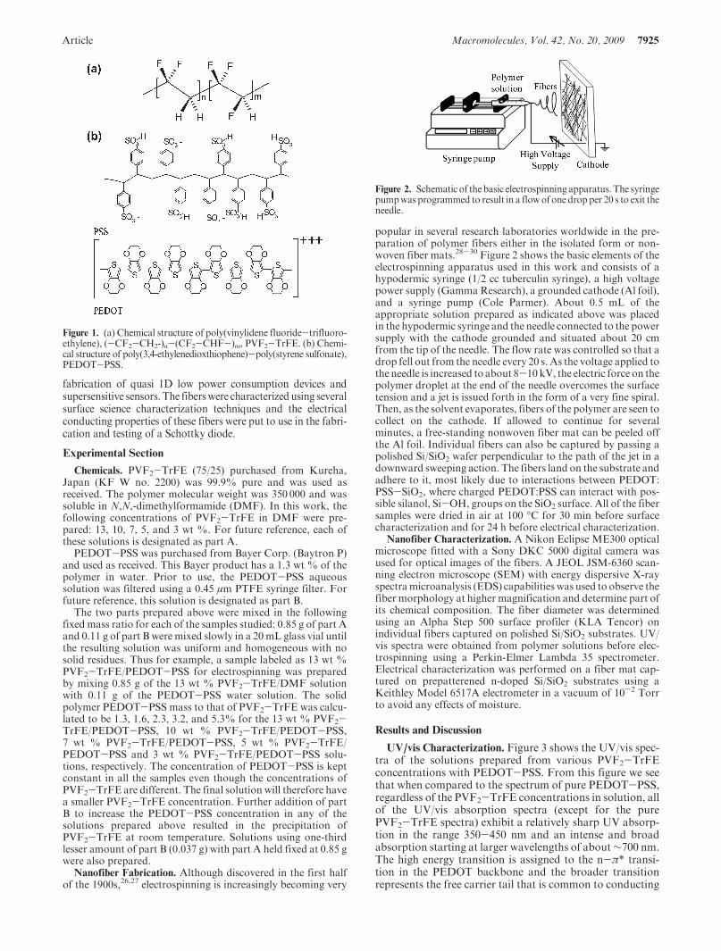
popular in several research laboratories worldwide in the pre-paration of polymer fibers either in the isolated form or non-woven fiber mats.28-30 Figure 2 shows the basic elements of theelectrospinning apparatus used in this work and consists of ahypodermic syringe (1/2 cc tuberculin syringe), a high voltagepower supply (GammaResearch), a grounded cathode (Al foil),and a syringe pump (Cole Parmer). About 0.5 mL of theappropriate solution prepared as indicated above was placedin the hypodermic syringe and the needle connected to the powersupply with the cathode grounded and situated about 20 cmfrom the tip of the needle. The flow rate was controlled so that adrop fell out from the needle every 20 s. As the voltage applied tothe needle is increased to about 8-10 kV, the electric force on thepolymer droplet at the end of the needle overcomes the surfacetension and a jet is issued forth in the form of a very fine spiral.Then, as the solvent evaporates, fibers of the polymer are seen tocollect on the cathode. If allowed to continue for severalminutes, a free-standing nonwoven fiber mat can be peeled offthe Al foil. Individual fibers can also be captured by passing apolished Si/SiO2 wafer perpendicular to the path of the jet in adownward sweeping action. The fibers land on the substrate andadhere to it, most likely due to interactions between PEDOT:PSS-SiO2, where charged PEDOT:PSS can interact with pos-sible silanol, Si-OH, groups on the SiO2 surface. All of the fibersamples were dried in air at 100 �C for 30 min before surfacecharacterization and for 24 h before electrical characterization.
Nanofiber Characterization. A Nikon Eclipse ME300 opticalmicroscope fitted with a Sony DKC 5000 digital camera wasused for optical images of the fibers. A JEOL JSM-6360 scan-ning electron microscope (SEM) with energy dispersive X-rayspectramicroanalysis (EDS) capabilities was used to observe thefiber morphology at higher magnification and determine part ofits chemical composition. The fiber diameter was determinedusing an Alpha Step 500 surface profiler (KLA Tencor) onindividual fibers captured on polished Si/SiO2 substrates. UV/vis spectra were obtained from polymer solutions before elec-trospinning using a Perkin-Elmer Lambda 35 spectrometer.Electrical characterization was performed on a fiber mat cap-tured on prepatterened n-doped Si/SiO2 substrates using aKeithley Model 6517A electrometer in a vacuum of 10-2 Torrto avoid any effects of moisture.
Results and Discussion
UV/vis Characterization. Figure 3 shows the UV/vis spec-tra of the solutions prepared from various PVF2-TrFEconcentrations with PEDOT-PSS. From this figure we seethat when compared to the spectrum of pure PEDOT-PSS,regardless of the PVF2-TrFE concentrations in solution, allof the UV/vis absorption spectra (except for the purePVF2-TrFE spectra) exhibit a relatively sharp UV absorp-tion in the range 350-450 nm and an intense and broadabsorption starting at larger wavelengths of about∼700 nm.The high energy transition is assigned to the n-π* transi-tion in the PEDOT backbone and the broader transitionrepresents the free carrier tail that is common to conducting
Figure 1. (a) Chemical structure of poly(vinylidene fluoride-trifluoro-ethylene), (-CF2-CH2-)n-(CF2-CHF-)m, PVF2-TrFE. (b) Chemi-cal structure of poly(3,4-ethylenedioxthiophene)-poly(styrene sulfonate),PEDOT-PSS.
Figure 2. Schematic of thebasic electrospinning apparatus. The syringepumpwas programmed to result in a flowof one dropper 20 s to exit theneedle.
7926 Macromolecules, Vol. 42, No. 20, 2009 Martı́nez et al.
polymers.31 These results imply that the PEDOT-PSS isuniformly incorporated as a composite in the solution.Further observation that the solutions once prepared andstored in glass vials, stayed homogeneous for several weekswith no indication of phase separation of the PVF2-TrFE/DMF and PEDOT-PSS water components strengthens theclaim that the PEDOT-PSS is well dispersed in thePVF2-TrFE/DMF solution.
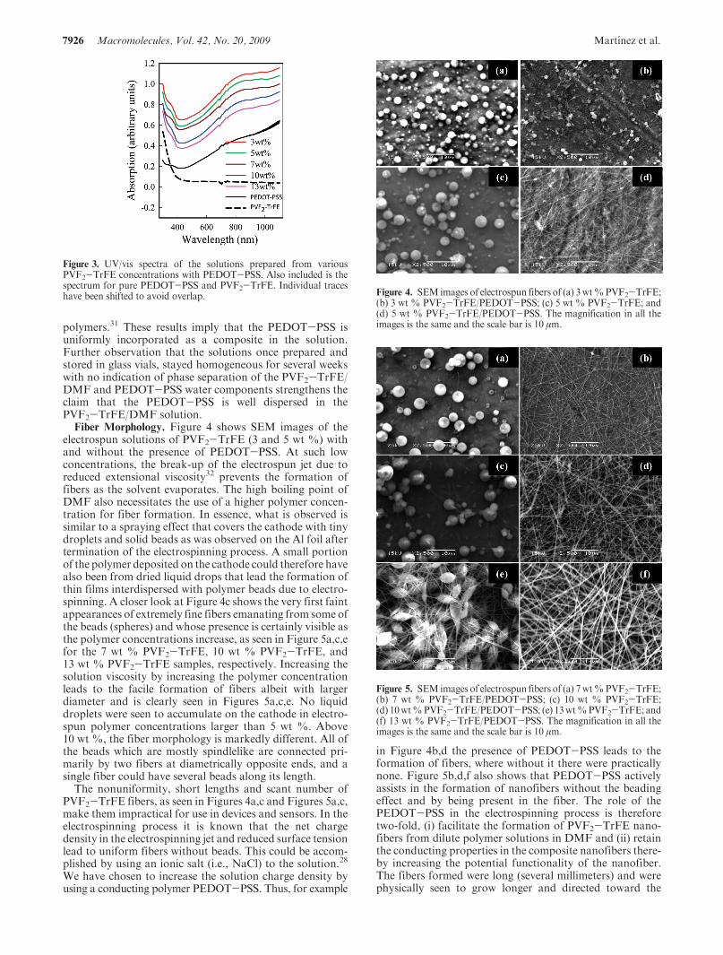
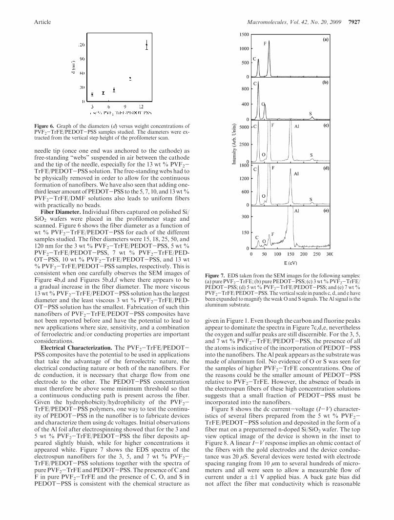
Fiber Morphology. Figure 4 shows SEM images of theelectrospun solutions of PVF2-TrFE (3 and 5 wt %) withand without the presence of PEDOT-PSS. At such lowconcentrations, the break-up of the electrospun jet due toreduced extensional viscosity32 prevents the formation offibers as the solvent evaporates. The high boiling point ofDMF also necessitates the use of a higher polymer concen-tration for fiber formation. In essence, what is observed issimilar to a spraying effect that covers the cathode with tinydroplets and solid beads as was observed on the Al foil aftertermination of the electrospinning process. A small portionof the polymer deposited on the cathode could therefore havealso been from dried liquid drops that lead the formation ofthin films interdispersed with polymer beads due to electro-spinning. A closer look at Figure 4c shows the very first faintappearances of extremely fine fibers emanating from some ofthe beads (spheres) and whose presence is certainly visible asthe polymer concentrations increase, as seen in Figure 5a,c,efor the 7 wt % PVF2-TrFE, 10 wt % PVF2-TrFE, and13 wt % PVF2-TrFE samples, respectively. Increasing thesolution viscosity by increasing the polymer concentrationleads to the facile formation of fibers albeit with largerdiameter and is clearly seen in Figures 5a,c,e. No liquiddroplets were seen to accumulate on the cathode in electro-spun polymer concentrations larger than 5 wt %. Above10 wt %, the fiber morphology is markedly different. All ofthe beads which are mostly spindlelike are connected pri-marily by two fibers at diametrically opposite ends, and asingle fiber could have several beads along its length.
The nonuniformity, short lengths and scant number ofPVF2-TrFE fibers, as seen in Figures 4a,c and Figures 5a,c,make them impractical for use in devices and sensors. In theelectrospinning process it is known that the net chargedensity in the electrospinning jet and reduced surface tensionlead to uniform fibers without beads. This could be accom-plished by using an ionic salt (i.e., NaCl) to the solution.28
We have chosen to increase the solution charge density byusing a conducting polymer PEDOT-PSS. Thus, for example
in Figure 4b,d the presence of PEDOT-PSS leads to theformation of fibers, where without it there were practicallynone. Figure 5b,d,f also shows that PEDOT-PSS activelyassists in the formation of nanofibers without the beadingeffect and by being present in the fiber. The role of thePEDOT-PSS in the electrospinning process is thereforetwo-fold, (i) facilitate the formation of PVF2-TrFE nano-fibers from dilute polymer solutions in DMF and (ii) retainthe conducting properties in the composite nanofibers there-by increasing the potential functionality of the nanofiber.The fibers formed were long (several millimeters) and werephysically seen to grow longer and directed toward the
Figure 3. UV/vis spectra of the solutions prepared from variousPVF2-TrFE concentrations with PEDOT-PSS. Also included is thespectrum for pure PEDOT-PSS and PVF2-TrFE. Individual traceshave been shifted to avoid overlap. Figure 4. SEM images of electrospun fibers of (a) 3wt%PVF2-TrFE;
(b) 3 wt % PVF2-TrFE/PEDOT-PSS; (c) 5 wt % PVF2-TrFE; and(d) 5 wt % PVF2-TrFE/PEDOT-PSS. The magnification in all theimages is the same and the scale bar is 10 μm.
Figure 5. SEM images of electrospun fibers of (a) 7wt%PVF2-TrFE;(b) 7 wt % PVF2-TrFE/PEDOT-PSS; (c) 10 wt % PVF2-TrFE;(d) 10wt%PVF2-TrFE/PEDOT-PSS; (e) 13wt%PVF2-TrFE; and(f) 13 wt % PVF2-TrFE/PEDOT-PSS. The magnification in all theimages is the same and the scale bar is 10 μm.
Article Macromolecules, Vol. 42, No. 20, 2009 7927
needle tip (once one end was anchored to the cathode) asfree-standing “webs” suspended in air between the cathodeand the tip of the needle, especially for the 13 wt % PVF2-TrFE/PEDOT-PSS solution. The free-standingwebs had tobe physically removed in order to allow for the continuousformation of nanofibers. We have also seen that adding one-third lesser amount ofPEDOT-PSS to the 5, 7, 10, and 13wt%PVF2-TrFE/DMF solutions also leads to uniform fiberswith practically no beads.
Fiber Diameter. Individual fibers captured on polished Si/SiO2 wafers were placed in the profilometer stage andscanned. Figure 6 shows the fiber diameter as a function ofwt % PVF2-TrFE/PEDOT-PSS for each of the differentsamples studied. The fiber diameters were 15, 18, 25, 50, and120 nm for the 3 wt % PVF2-TrFE/PEDOT-PSS, 5 wt %PVF2-TrFE/PEDOT-PSS, 7 wt % PVF2-TrFE/PED-OT-PSS, 10 wt % PVF2-TrFE/PEDOT-PSS, and 13 wt% PVF2-TrFE/PEDOT-PSS samples, respectively. This isconsistent when one carefully observes the SEM images ofFigure 4b,d and Figures 5b,d,f where there appears to bea gradual increase in the fiber diameter. The more viscous13 wt%PVF2-TrFE/PEDOT-PSS solution has the largestdiameter and the least viscous 3 wt % PVF2-TrFE/PED-OT-PSS solution has the smallest. Fabrication of such thinnanofibers of PVF2-TrFE/PEDOT-PSS composites havenot been reported before and have the potential to lead tonew applications where size, sensitivity, and a combinationof ferroelectric and/or conducting properties are importantconsiderations.
Electrical Characterization. The PVF2-TrFE/PEDOT-PSS composites have the potential to be used in applicationsthat take the advantage of the ferroelectric nature, theelectrical conducting nature or both of the nanofibers. Fordc conduction, it is necessary that charge flow from oneelectrode to the other. The PEDOT-PSS concentrationmust therefore be above some minimum threshold so thata continuous conducting path is present across the fiber.Given the hydrophobicity/hydrophilicity of the PVF2-TrFE/PEDOT-PSS polymers, one way to test the continu-ity of PEDOT-PSS in the nanofiber is to fabricate devicesand characterize them using dc voltages. Initial observationsof the Al foil after electrospinning showed that for the 3 and5 wt % PVF2-TrFE/PEDOT-PSS the fiber deposits ap-peared slightly bluish, while for higher concentrations itappeared white. Figure 7 shows the EDS spectra of theelectrospun nanofibers for the 3, 5, and 7 wt % PVF2-TrFE/PEDOT-PSS solutions together with the spectra ofpure PVF2-TrFE and PEDOT-PSS. The presence of C andF in pure PVF2-TrFE and the presence of C, O, and S inPEDOT-PSS is consistent with the chemical structure as
given in Figure 1. Even though the carbon and fluorine peaksappear to dominate the spectra in Figure 7c,d,e, neverthelessthe oxygen and sulfur peaks are still discernible. For the 3, 5,and 7 wt % PVF2-TrFE/PEDOT-PSS, the presence of allthe atoms is indicative of the incorporation of PEDOT-PSSinto the nanofibers. TheAl peak appears as the substratewasmade of aluminum foil. No evidence of O or S was seen forthe samples of higher PVF2-TrFE concentrations. One ofthe reasons could be the smaller amount of PEDOT-PSSrelative to PVF2-TrFE. However, the absence of beads inthe electrospun fibers of these high concentration solutionssuggests that a small fraction of PEDOT-PSS must beincorporated into the nanofibers.
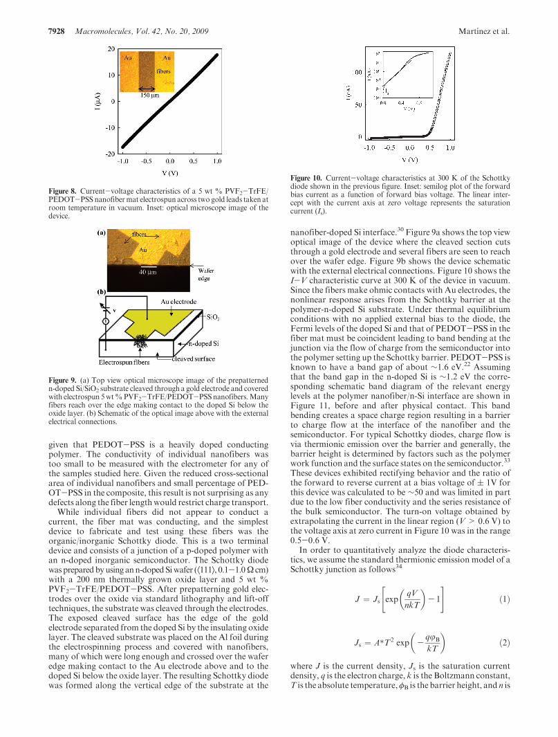
Figure 8 shows the dc current-voltage (I-V) character-istics of several fibers prepared from the 5 wt % PVF2-TrFE/PEDOT-PSS solution and deposited in the form of afiber mat on a prepatterned n-doped Si/SiO2 wafer. The topview optical image of the device is shown in the inset toFigure 8. A linear I-V response implies an ohmic contact ofthe fibers with the gold electrodes and the device conduc-tance was 20 μS. Several devices were tested with electrodespacing ranging from 10 μm to several hundreds of micro-meters and all were seen to allow a measurable flow ofcurrent under a (1 V applied bias. A back gate bias didnot affect the fiber mat conductivity which is reasonable
Figure 6. Graph of the diameters (d) versus weight concentrations ofPVF2-TrFE/PEDOT-PSS samples studied. The diameters were ex-tracted from the vertical step height of the profilometer scan.
Figure 7. EDS taken from the SEM images for the following samples:(a) pure PVF2-TrFE; (b) pure PEDOT-PSS; (c) 3 wt%PVF2-TrFE/PEDOT-PSS; (d) 5 wt% PVF2-TrFE/PEDOT-PSS; and (e) 7 wt%PVF2-TrFE/PEDOT-PSS. The vertical scale in panels c, d, and e havebeen expanded tomagnify theweakO and S signals. TheAl signal is thealuminum substrate.
7928 Macromolecules, Vol. 42, No. 20, 2009 Martı́nez et al.
given that PEDOT-PSS is a heavily doped conductingpolymer. The conductivity of individual nanofibers wastoo small to be measured with the electrometer for any ofthe samples studied here. Given the reduced cross-sectionalarea of individual nanofibers and small percentage of PED-OT-PSS in the composite, this result is not surprising as anydefects along the fiber lengthwould restrict charge transport.
While individual fibers did not appear to conduct acurrent, the fiber mat was conducting, and the simplestdevice to fabricate and test using these fibers was theorganic/inorganic Schottky diode. This is a two terminaldevice and consists of a junction of a p-doped polymer withan n-doped inorganic semiconductor. The Schottky diodewaspreparedbyusing ann-dopedSiwafer (Æ111æ, 0.1-1.0Ω cm)with a 200 nm thermally grown oxide layer and 5 wt %PVF2-TrFE/PEDOT-PSS. After prepatterning gold elec-trodes over the oxide via standard lithography and lift-offtechniques, the substrate was cleaved through the electrodes.The exposed cleaved surface has the edge of the goldelectrode separated from the doped Si by the insulating oxidelayer. The cleaved substrate was placed on the Al foil duringthe electrospinning process and covered with nanofibers,many of which were long enough and crossed over the waferedge making contact to the Au electrode above and to thedoped Si below the oxide layer. The resulting Schottky diodewas formed along the vertical edge of the substrate at the
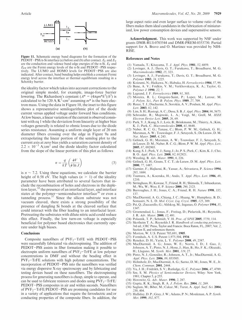
nanofiber-doped Si interface.30 Figure 9a shows the top viewoptical image of the device where the cleaved section cutsthrough a gold electrode and several fibers are seen to reachover the wafer edge. Figure 9b shows the device schematicwith the external electrical connections. Figure 10 shows theI-V characteristic curve at 300 K of the device in vacuum.Since the fibers make ohmic contacts with Au electrodes, thenonlinear response arises from the Schottky barrier at thepolymer-n-doped Si substrate. Under thermal equilibriumconditions with no applied external bias to the diode, theFermi levels of the doped Si and that of PEDOT-PSS in thefiber mat must be coincident leading to band bending at thejunction via the flow of charge from the semiconductor intothe polymer setting up the Schottky barrier. PEDOT-PSS isknown to have a band gap of about ∼1.6 eV.22 Assumingthat the band gap in the n-doped Si is ∼1.2 eV the corre-sponding schematic band diagram of the relevant energylevels at the polymer nanofiber/n-Si interface are shown inFigure 11, before and after physical contact. This bandbending creates a space charge region resulting in a barrierto charge flow at the interface of the nanofiber and thesemiconductor. For typical Schottky diodes, charge flow isvia thermionic emission over the barrier and generally, thebarrier height is determined by factors such as the polymerwork function and the surface states on the semiconductor.33
These devices exhibited rectifying behavior and the ratio ofthe forward to reverse current at a bias voltage of ( 1V forthis device was calculated to be ∼50 and was limited in partdue to the low fiber conductivity and the series resistance ofthe bulk semiconductor. The turn-on voltage obtained byextrapolating the current in the linear region (V> 0.6 V) tothe voltage axis at zero current in Figure 10 was in the range0.5-0.6 V.
In order to quantitatively analyze the diode characteris-tics, we assume the standard thermionic emission model of aSchottky junction as follows34
J ¼ Js expqV
nkT
� �- 1
" #ð1Þ
Js ¼ A�T2 exp -qjB
kT
� �ð2Þ
where J is the current density, Js is the saturation currentdensity, q is the electron charge, k is the Boltzmann constant,T is the absolute temperature,φB is the barrier height, and n is
Figure 8. Current-voltage characteristics of a 5 wt % PVF2-TrFE/PEDOT-PSS nanofibermat electrospun across two gold leads taken atroom temperature in vacuum. Inset: optical microscope image of thedevice.
Figure 9. (a) Top view optical microscope image of the prepatternedn-doped Si/SiO2 substrate cleaved through a gold electrode and coveredwith electrospun 5wt%PVF2-TrFE/PEDOT-PSSnanofibers.Manyfibers reach over the edge making contact to the doped Si below theoxide layer. (b) Schematic of the optical image above with the externalelectrical connections.
Figure 10. Current-voltage characteristics at 300 K of the Schottkydiode shown in the previous figure. Inset: semilog plot of the forwardbias current as a function of forward bias voltage. The linear inter-cept with the current axis at zero voltage represents the saturationcurrent (Is).
Article Macromolecules, Vol. 42, No. 20, 2009 7929
the ideality factorwhich takes into account corrections to theoriginal simple model, for example, image-force barrierlowering. The Richardson’s constant (A*= (4πqm*k2)/h3) iscalculated to be 120 A/K2-cm2 assuming m* is the bare elec-tronmass. Using the data in Figure 10, the inset to this figureshows a representative semilogarithmic plot of the diodecurrent versus applied voltage under forward bias conditions.At lowbiases, a linearvariationof the current isobservedconsis-tentwith eq 1while the deviation from linearity at higher biasvoltages generally is related to ohmic losses due to the diodeseries resistance. Assuming a uniform single layer of 20 nmdiameter fibers crossing over the edge in Figure 9a andextrapolating the linear portion of the semilog plot to thecurrent axis at zero bias yields a saturation current density of2.2 � 10-3 A/cm2 and the diode ideality factor calculatedfrom the slope of the linear portion of this plot as follows
n ¼ q
kT
DVD ln J
� �ð3Þ
is n ∼ 7.2. Using these equations, we calculate the barrierheight of 0.58 eV. The high values (n > 1) of the idealityparameter have been attributed to several factors that in-clude the recombination of holes and electrons in the deple-tion layer,35 the presence of an interfacial layer, and interfacestates at the polymer-semiconductor interface36 or even atunneling process.37 Since the silicon substrate was notvacuum cleaved, there exists a strong possibility of thepresence of dangling Si bonds at the cleaved surface thatcould interact with the fiber leading to an interfacial layer.Pretreating the substrates with dilute nitric acid could reducethis effect. Finally, the low turn-on voltage is especiallybeneficial for polymer based electronics that currently ope-rate under high biases.
Conclusions
Composite nanofibers of PVF2-TrFE with PEDOT-PSSwere successfully fabricated via electrospinning. The addition ofPEDOT-PSS assists in fiber formation making it possible toelectrospin uniform nanofibers of PVF2-TrFE at low polymerconcentrations in DMF and without the beading effect inPVF2-TrFE solutions with high polymer concentrations. Theincorporation of PEDOT-PSS into the nanofibers was verifiedvia energy dispersive X-ray spectroscopy and by fabricating andtesting devices based on these nanofibers. The electrospinningprocess for generating nanofibers is cheap, simple to operate, andcan be used to fabricate resistors and diodes using PVF2-TrFE/PEDOT-PSS composites in air and within seconds. Nanofibersof PVF2-TrFE/PEDOT-PSS are promising candidates for usein a variety of applications that require the ferroelectric and/orconducting properties of the composite fibers. In addition, the
large aspect ratio and even larger surface to volume ratio of thefibers makes them ideal candidates in the fabrication of miniatur-ized, low power consumption devices and supersensitive sensors.
Acknowledgment. This work was supported by NSF undergrants DMR-RUI-0703544 and DMR-PREM-0353730. Partialsupport for A. Bravo and O. Martinez was provided by NIH-RISE.
References and Notes
(1) Yamada, T.; Kitayama, T. J. Appl. Phys. 1981, 52, 6859.(2) Lovinger, A. J.; Davis, G. T.; Furukawa, T.; Broadhurst, M. G.
Macromolecules 1982, 15, 323.(3) Lovinger, A. J.; Furukawa, T.; Davis, G. T.; Broadhurst, M. G.
Polymer 1983, 24, 1225.(4) Koizumi, N.; Haikawa, N.; Habuka, H. Ferroelectrics 1984, 57, 99.(5) Bune, A. V.; Fridkin, V. M.; Verkhovskaya, K. A.; Taylor, G.
Polymer J. 1990, 22, 7.(6) Legrand, J. F. Ferroelectrics 1989, 91, 303.(7) Moreira, R. L.; Gregoire-Saint, P.; Lopez, M.; Latour, M.
J. Polym. Sci., Part B: Polym. Phys. 1989, 27, 709.(8) Reece, T. J.;Ducharme, S.; Sorokin,A.V.; Poulsen,M.Appl. Phys.
Lett. 2003, 82, 142.(9) Lim, S.H.; Rastogi, A. C.; Desu, S. B. J. Appl. Phys. 2004, 96, 5673.
(10) Schroeder, R.; Majewski, L. A.; Voigt, M.; Grell, M. IEEEElectron Device Lett. 2005, 26, 69.
(11) Park,Y. J.;Kang, S. J.; Lotz, B.; Brinkmann,M.; Thierry, A.;Kim,K. J.; Park, C. Macromolecules 2008, 41, 8648.
(12) Naber, R. C. G.; Tanase, C.; Blom, P. W. M.; Gelinck, G. H.;Marsman, A.W.; Touwslager, F. J.; Setayesh, S.; De Leeuw,D.M.Nat. Mater. 2005, 4, 243.
(13) Gelinck, G. H.; Marsman, A. W.; Touwslaer, F. J.; Setayesh, S.;deLeeuw,D.M.;Naber,R.C.G.; Blom,P.W.M.Appl. Phys. Lett.2005, 87, 092903.
(14) Kang, S. J.; Park,Y. J.; Sung, J.; Jo, P. S.; Park,C.;Kim,K. J.; Cho,B. O. Appl. Phys. Lett. 2008, 92, 012921.
(15) Wessling, B. Adv. Mater. 1991, 6, 226.(16) Gelinck, G. H.; Geuns, T. C. T.; de Leeuw, D.M.Appl. Phys. Lett.
2000, 77, 1487.(17) Garnier, F.; Hajlaoui, R.; Yassar, A.; Srivastava, P. Science 1994,
265, 1684.(18) Tsumura, A.; Koezuka, H.; Ando, T. Appl. Phys. Lett. 1986, 49,
1210.(19) Sirringhaus,H.;Kawase, T.; Friend,R.H.; Shimoda,T.; Inbasekaran,
M.; Wu, W.; Woo, E. P. Science 2000, 290, 2123.(20) Burroughes, J. H.; Jones, C. A.; Friend, R. H. Nature 1998, 335,
137.(21) MacDiarmid, A. G.; Chiang, J. C.; Huang, W.; Humphrey, B. D.;
Somasiri, N. L. D. Mol. Cryst. Liq. Cryst. 1985, 125, 309.(22) Pei, Q.; Zuccarello, G.; Ahlskog,M.; Inganas,O.Polymer 1994, 35,
1347.(23) Groenendaal, L.; Jonas, F.; Freitag, D.; Pielartzik, H.; Reynolds,
J. R. Adv. Mater. 2000, 12, 481.(24) Polasnik, T. P.; Schmidt, V. H. Proc. of SPIE 2005, 5759, 114.(25) Skotheim T. A.; Reynolds J. R.Handbook of conducting polymers,
3rd ed.; CRC Press, Taylor and Francis: Boca Raton, FL, 2007; Vol. 2,Section II, and references therein.
(26) Morton, W. U.S. Patent 705,691, 1905.(27) Formhals, A. U.S. Patent 1,975,504, 1934.(28) Reneker, D. H.; Yarin, L. Y. Polymer 2008, 49, 2387.(29) MacDiarmid, A. G.; Jones, W. E.; Norris, I. D.; J. Gao, J.;
Johnson,A. T.; Pinto,N. J.; Hone, J.; Han, B.; Ho, F.K.; Okuzaki,H.; Llaguno, M. Synth. Met. 2001, 119, 27.
(30) Pinto, N. J.; Gonz�alez, R.; Johnson, A. T., Jr.; MacDiarmid, A. G.Appl. Phys. Lett. 2006, 89, 033505.
(31) Hohnholz, D.;MacDiarmid, A. G.; Sarno, D.M.; Jones,W. E., Jr.Chem. Commun. 2001, 2444.
(32) Yu, J. H.; Fridrikh, S. V.; Rutledge, G. C. Polymer 2006, 47, 4789.(33) Sze, S. M. Physics of Semiconductor Devices; Wiley: New York,
1981; Chapter 5, p 255.(34) Horowitz, G. Adv. Mater. 1990, 2, 287.(35) Gupta, R. K.; Singh, R. A. J. Polym. Res. 2004, 11, 269.(36) Saglam,M.; Biber, M.; Cakar, M.; Turut, A. Appl. Surf. Sci. 2004,
230, 404.(37) Halliday,D. P.;Gray, J.W.; Adams, P.N.;Monkman,A. P.Synth.
Met. 1999, 102, 877.
Figure 11. Schematic energy band diagrams for the formation of thePEDOT-PSS/n-Si interface (a) before and (b) after contact.EC andEV
are the conduction and valence band edge energies of the n-Si. EF andEFP are the Fermi energy levels of the n-Si and PEDOT-PSS respec-tively. The LUMO and HOMO levels for PEDOT-PSS are alsoindicated. After contact, band bending helps establish a constant Fermienergy level across the interface at thermal equilibrium resulting in aSchottky barrier.
Related Documents


![ars.els-cdn.com · Web view[6] X. Liu, W. Wu, Z. Gu, Poly (3,4-ethylenedioxythiophene) promotes direct electron transfer at the interface between Shewanella loihica and the anode](https://static.cupdf.com/doc/110x72/6063c230a674eb2fad310ddc/arsels-cdncom-web-view-6-x-liu-w-wu-z-gu-poly-34-ethylenedioxythiophene.jpg)