Sensors 2020, 20, 2716; doi:10.3390/s20092716 www.mdpi.com/journal/sensors Article Fabrication of Microbolometer Arrays Based on Polymorphous Silicon–Germanium Ricardo Jimenez 1 , Mario Moreno 1, *, Alfonso Torres 1 , Alfredo Morales 1 , Arturo Ponce 1,2 , Daniel Ferrusca 1 , Jose Rangel-Magdaleno 1 , Jorge Castro-Ramos 1 , Julio Hernandez-Perez 1 and Eduardo Cano 1 1 Electronics Group, National Institute of Astrophysics, Optics and Electronics, Puebla 72840, Mexico; [email protected] (R.J.); [email protected] (A.T.); [email protected] (A.M.); [email protected] (A.P.); [email protected] (D.F.); [email protected] (J.R.‐M.); [email protected] (J.C.‐R.); [email protected] (J.H.‐P.); [email protected] (E.C.) 2 Department of Physics and Astronomy, University of Texas at San Antonio, San Antonio, TX 78249, USA * Correspondence: [email protected] Received: 30 March 2020; Accepted: 24 April 2020; Published: 9 May 2020 Abstract: This work reports the development of arrays of infrared sensors (microbolometers) using a hydrogenated polymorphous silicon–germanium alloy (pm‐SixGe1‐x:H). Basically, polymorphous semiconductors consist of an amorphous semiconductor matrix with embedded nanocrystals of about 2–3 nm. The pm‐SixGe1‐x:H alloy studied has a high temperature coefficient of resistance (TCR) of 4.08%/K and conductivity of 1.5 × 10 −5 S∙cm −1 . Deposition of thermosensing film was made by plasma‐enhanced chemical vapor deposition (PECVD) at 200 °C, while the area of the devices is 50 × 50 µm 2 with a fill factor of 81%. Finally, an array of 19 × 20 microbolometers was packaged for electrical characterization. Voltage responsivity values were obtained in the range of 4 × 10 4 V/W and detectivity around 2 × 10 7 cm∙Hz 1/2 /W with a polarization current of 70 µA at a chopper frequency of 30 Hz. A minimum value of 2 × 10 −10 W/Hz 1/2 noise equivalent power was obtained at room temperature. In addition, it was found that all the tested devices responded to incident infrared radiation, proving that the structure and mechanical stability are excellent. Keywords: infrared; sensor; microbolometer; array; polymorphous; silicon; germanium; plasma‐ enhanced chemical vapor deposition 1. Introduction Semiconductor materials with characteristics of low resistivity and high temperature coefficient of resistance (TCR) are important for detection of infrared radiation by uncooled microbolometers, which are widely used in the range of 8–12 µm, known as LWIR (long‐wave infrared). A microbolometer is a thermal detector where a resistive membrane absorbs infrared radiation, which increases its temperature. For semiconductor materials, the increase in temperature reduces the resistance of the membrane and the measurement of the change of resistance is the output of the sensor. A high TCR is desirable to increase the sensitivity of the device or maintaining it when it is desired to reduce the pixel area. On the other hand, a low resistivity makes it easier to read the pixels with the associated ROIC (readout integrated circuit). In addition, the resistivity of the material directly influences the 1/f noise and consequently the performance of the devices. In relation to the electrical characteristics described above, several materials have been studied for their application as thermosensing films, including carbon nanotubes and other organic compounds with TCR values of about 2.1%–3.1%/K [1–3], poly‐SiGe (0.68%–2%/K) [4], Y‐Ba‐Cu‐O (~3.3%/K) [5], metal films Pt (~0.14%/K) [6], Ti (~0.35%/K) [7,8]; as well ZnO has shown high TCR (~10.4%/K) in thin films, but without reported experimental results on devices [9].

Welcome message from author
This document is posted to help you gain knowledge. Please leave a comment to let me know what you think about it! Share it to your friends and learn new things together.
Transcript

Sensors 2020, 20, 2716; doi:10.3390/s20092716 www.mdpi.com/journal/sensors
Article
Fabrication of Microbolometer Arrays Based on
Polymorphous Silicon–Germanium
Ricardo Jimenez 1, Mario Moreno 1,*, Alfonso Torres 1, Alfredo Morales 1, Arturo Ponce 1,2, Daniel
Ferrusca 1, Jose Rangel-Magdaleno 1, Jorge Castro-Ramos 1, Julio Hernandez-Perez 1 and Eduardo
Cano 1
1 Electronics Group, National Institute of Astrophysics, Optics and Electronics, Puebla 72840, Mexico;
[email protected] (R.J.); [email protected] (A.T.); [email protected] (A.M.); [email protected]
(A.P.); [email protected] (D.F.); [email protected] (J.R.‐M.); [email protected] (J.C.‐R.);
[email protected] (J.H.‐P.); [email protected] (E.C.) 2 Department of Physics and Astronomy, University of Texas at San Antonio, San Antonio, TX 78249, USA
* Correspondence: [email protected]
Received: 30 March 2020; Accepted: 24 April 2020; Published: 9 May 2020
Abstract: This work reports the development of arrays of infrared sensors (microbolometers) using
a hydrogenated polymorphous silicon–germanium alloy (pm‐SixGe1‐x:H). Basically, polymorphous
semiconductors consist of an amorphous semiconductor matrix with embedded nanocrystals of
about 2–3 nm. The pm‐SixGe1‐x:H alloy studied has a high temperature coefficient of resistance (TCR)
of 4.08%/K and conductivity of 1.5 × 10⁻⁵ S∙cm−1. Deposition of thermosensing film was made by
plasma‐enhanced chemical vapor deposition (PECVD) at 200 °C, while the area of the devices is 50
× 50 µm2 with a fill factor of 81%. Finally, an array of 19 × 20 microbolometers was packaged for
electrical characterization. Voltage responsivity values were obtained in the range of 4 × 10⁴ V/W
and detectivity around 2 × 107 cm∙Hz1/2/W with a polarization current of 70 µA at a chopper
frequency of 30 Hz. A minimum value of 2 × 10⁻¹⁰ W/Hz1/2 noise equivalent power was obtained at
room temperature. In addition, it was found that all the tested devices responded to incident
infrared radiation, proving that the structure and mechanical stability are excellent.
Keywords: infrared; sensor; microbolometer; array; polymorphous; silicon; germanium; plasma‐
enhanced chemical vapor deposition
1. Introduction
Semiconductor materials with characteristics of low resistivity and high temperature coefficient
of resistance (TCR) are important for detection of infrared radiation by uncooled microbolometers,
which are widely used in the range of 8–12 µm, known as LWIR (long‐wave infrared). A
microbolometer is a thermal detector where a resistive membrane absorbs infrared radiation, which
increases its temperature. For semiconductor materials, the increase in temperature reduces the
resistance of the membrane and the measurement of the change of resistance is the output of the
sensor. A high TCR is desirable to increase the sensitivity of the device or maintaining it when it is
desired to reduce the pixel area. On the other hand, a low resistivity makes it easier to read the pixels
with the associated ROIC (readout integrated circuit). In addition, the resistivity of the material
directly influences the 1/f noise and consequently the performance of the devices.
In relation to the electrical characteristics described above, several materials have been studied
for their application as thermosensing films, including carbon nanotubes and other organic
compounds with TCR values of about 2.1%–3.1%/K [1–3], poly‐SiGe (0.68%–2%/K) [4], Y‐Ba‐Cu‐O
(~3.3%/K) [5], metal films Pt (~0.14%/K) [6], Ti (~0.35%/K) [7,8]; as well ZnO has shown high TCR
(~10.4%/K) in thin films, but without reported experimental results on devices [9].

Sensors 2020, 20, 2716 2 of 10
At the present time, vanadium oxide (VOx) (~2%/K) [10–16] and doped amorphous silicon (a‐Si)
with TCR values of 2%–5%/K [17–22] are the two main materials used as thermosensing films in
commercial microbolometers. However, amorphous silicon, usually doped with boron, is replacing
vanadium oxide in large commercial arrays. The reason is the full silicon complementary metal oxide
semiconductor (CMOS) processes compatibility and the larger TCR of amorphous silicon. This means
that large arrays can be fabricated in standard silicon CMOS facilities, and moreover, those arrays
contain devices with better performance characteristics.
In this work, we study the implementation in microbolometer arrays of a hydrogenated
polymorphous silicon‐germanium alloy (pm‐SixGe1‐x:H), which is a material composed of an
amorphous matrix with embedded nanocrystals in the range of 2–3 nm [23]. The presence of
nanocrystals reduces the density of states, improving the transport properties and the stability of the
material against radiation‐induced degradation (Staebler–Wronski effect) [24]. This was confirmed
with the results of aged polymorphous silicon (pm‐Si:H) solar cells by light‐soaking [25]. In pm‐
SixGe1‐x:H, the TCR can be easily modified with the silicon/germanium ratio of the alloy, and as a
consequence the 1/f noise is also modified [26,27]. This novel material is deposited by plasma‐
enhanced chemical vapor deposition (PECVD) at low temperature and pattern definition can be
performed by dry‐etching techniques, which are conventional steps in integrated circuits processing;
moreover, their TCR values are larger than those obtained in doped amorphous silicon. As a result,
pm‐SixGe1‐x:H is a material with full CMOS processes compatibility and can also be synthesized at
low temperatures, making it ideal for microbolometer implementation.
In previous work, titanium (Ti) electrodes were on the top of the membrane [28,29], however,
there were problems of stress mismatching between Ti and pm‐SixGe1‐x:H. Now we have decided to
replace the coplanar electrodes with Ti studs; in addition, an array of microbolometers with pixel
area of 50 × 50 µm2 was fabricated in order to study the stability of the structures and analyze their
performance quality.
2. Materials and Methods
2.1. Preparation Method of the Thermosensing Film
Deposition of pm‐SixGe1‐x:H was made in a plasma‐enhanced chemical vapor deposition
(PECVD) reactor AMP‐3300 from Applied Materials, Inc., Santa Clara, CA, USA, working at 110 kHz.
A mixture of silane (SiH4) and germane (GeH4) gases were diluted in hydrogen with a ratio of 1:20.
Nanocrystal formation is promoted when plasma conditions are close to powder regime [30], in that
sense we set a relatively high pressure inside the chamber. The whole set of conditions is listed in
Table 1.
Table 1. Deposition parameters for the pm‐SixGe1‐x:H layer.
GeH4 (sccm) SiH4 (sccm) H2 (sccm) Pressure (Torr) Power (mW/cm2) Temperature (C)
30 20 1000 1.2 90 200
2.2. Temperature Dependence of Conductivity
In order to measure dark conductivity as a function of temperature (T), a pm‐SixGe1‐x:H film
was deposited on top of coplanar titanium electrodes using Corning Glass 2947 as a substrate. The
geometry of the electrodes was 300 nm thick, 9.5 mm long, and separated by 2 mm. (T) of the films
was measured in the range of 300–400 K inside a vacuum thermostat VPF‐100 from Janis Research
Company, LLC, Woburn, M.A. USA, at 15 mTorr in steps of 10 K, while a ramp of 5 K/min was
employed. At every point, the sample was allowed to thermalize for 3 min before each measurement.
As humidity can play a major role in conductivity measurements [31], two heating ramps were
carried out, one to desorb humidity and the second for data collection. The conductivity in pm‐SixGe1‐
x:H shows a thermally activated Arrhenius behavior, which is related to activation energy (Ea)
through Equation (1), where k is the Boltzmann constant and 0 the conductivity prefactor [19].
Sensors 2020, 20, 2716 3 of 10
)./exp()( 0 kTET a (1)
Solving for Ea to fit the experimental data with a straight line, gives Equation (2):
./)()( 0 kTELnLn a (2)
The slope of the line gives Ea and the TCR is finally calculated using Equation (3):
.100)/( 2 kTETCR a (3)
Polymorphous silicon–germanium, like many semiconductors, exhibits a negative TCR (its
resistance decreases with temperature), although for convenience the absolute value will be
mentioned unless otherwise indicated.
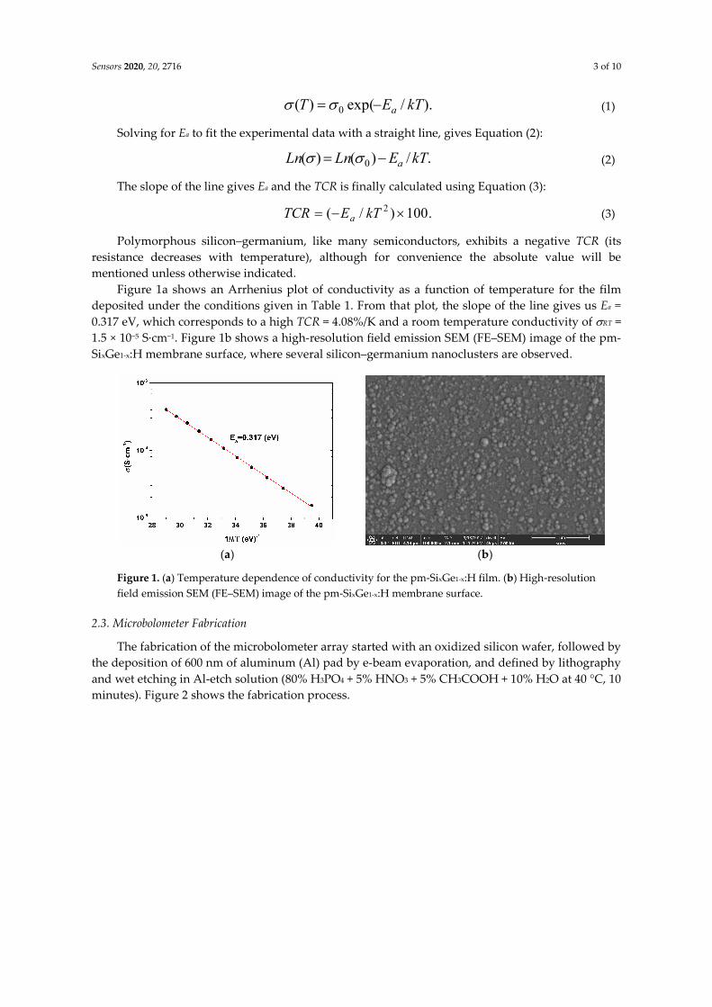
Figure 1a shows an Arrhenius plot of conductivity as a function of temperature for the film
deposited under the conditions given in Table 1. From that plot, the slope of the line gives us Ea =
0.317 eV, which corresponds to a high TCR = 4.08%/K and a room temperature conductivity of RT =
1.5 × 10⁻⁵ S∙cm−1. Figure 1b shows a high‐resolution field emission SEM (FE–SEM) image of the pm‐
SixGe1‐x:H membrane surface, where several silicon–germanium nanoclusters are observed.
(a)
(b)
Figure 1. (a) Temperature dependence of conductivity for the pm‐SixGe1‐x:H film. (b) High‐resolution
field emission SEM (FE–SEM) image of the pm‐SixGe1‐x:H membrane surface.
2.3. Microbolometer Fabrication
The fabrication of the microbolometer array started with an oxidized silicon wafer, followed by
the deposition of 600 nm of aluminum (Al) pad by e‐beam evaporation, and defined by lithography
and wet etching in Al‐etch solution (80% H3PO4 + 5% HNO3 + 5% CH3COOH + 10% H2O at 40 °C, 10
minutes). Figure 2 shows the fabrication process.

Sensors 2020, 20, 2716 4 of 10
(a)
(b)
(c)
(d)
(e)
(f)
Figure 2. Fabrication process flow: (a) aluminum deposition and patterning (columns); (b) after
deposition of the double layer of dielectric, a second layer deposition of aluminum (rows and mirror)
followed; (c) polyimide deposition and opening of holes for contacts; (d) pm‐SixGe1‐x:H deposition
and patterning; (e) deposition of titanium studs; (f) dry etching of the sacrificial polyimide layer.
Then, spin‐on glass (SOG) 700B diluted in water at 50% was deposited on the wafer and cured
at 250 °C for 2 h in air to obtain a layer with a refractive index n = 1.462 and a thickness of 180 nm that
helps to planarize the surface. A refractive index close to that of thermal SiO2 assures a dense film
with a low number of voids and defects. We avoided a thicker layer of SOG due to cracking and
peeling issues by adding a second dielectric 120 nm‐thick silicon nitride (SiNx) layer by PECVD. All
film depositions by PECVD were performed in a system working at 110 kHz and 200 °C.
After that, a second Al metal layer with a thickness of 600 nm was evaporated and patterned by
liftoff. The first Al layer defined the columns and the second layer defined the rows and the reflective
mirror. Then, a 50 nm‐thick SiNx layer was deposited by PECVD to protect the aluminum pads from
a later step of wet etching. A layer of polyimide (PI‐2610) was spin‐coated on the silicon wafer to
form a 2.5 µm‐thick gap, as part of a resonant quarter‐wavelength cavity to improve absorption in
the LWIR band. This Fabry–Perot resonant cavity was tuned at 10 µm wavelength by adjusting
polyimide thickness d according to the relation d = /4n + N/2n, where N = 0, 1, 2, ... and n is the
refractive index of the vacuum (after polyimide removal). Polyimide was soft‐backed in a nitrogen
environment with a ramp of 5 °C/min and finally cured at 250 °C for 2 h in fresh air to avoid the
formation of bubbles.
A hard Al mask, 150 nm thick, was evaporated and patterned by wet etching; the polyimide was
then patterned with oxygen plasma by reactive ion etching (RIE) using an AME‐8110 tool from
Applied Materials, Inc., Santa Clara, CA, USA, in order to open contact windows. After that, Al‐etch
solution was employed to remove the aluminum hard mask. The following step consisted of
patterning the SiNx and SOG layers through the contact windows using CF4‐based plasma with a
micro‐RIE series 800 reactor from Technics. Then, the thermosensing film 400 nm thick was deposited
as described earlier (Section 2.1). In order to shape the membranes, the CF4 plasma was employed to
pattern the pm‐SixGe1‐x:H film by the RIE technique.
After that, a 600 nm‐thick Ti layer was evaporated and patterned by liftoff to create supporting
studs. This structure thermally isolates the membrane from the substrate. Furthermore, Ti has a low
thermal conductivity of 21.9 W/mK and is a material commonly used in the Si–CMOS process.
Finally, the silicon wafer was diced and the polyimide sacrificial layer was removed by oxygen
plasma using a barrel asher L2101 from Branson/IPC, Hayward, CA, USA.
2.4. Experimental Setup
To perform the characterization, a single die with an array of 19 × 20 elements was placed in a
DIP‐40 package from Kyocera Corporation, Kyoto, Japan and bonded with gold wires.
Microbolometers were then mounted inside a vacuum chamber MTD‐150 from Lake Shore
Cryotronics, Inc., Westerville, OH, USA (Figure 3). It was evacuated to 20 mTorr and measurements

Sensors 2020, 20, 2716 5 of 10
were carried out at 300 K. For voltage responsivity (v) measurements, the array was illuminated
with a cavity blackbody radiator using a silicon carbide (SiC) rod from Kanthal Globar as a broadband
infrared source. Radiation comes out through a one inch aperture, which was then modulated at 30
Hz with a chopper wheel SR540 from Stanford Research Systems, Sunnyvale, OH, USA.
.
Figure 3. Array of microbolometers wire‐bonded to a DIP‐40 package and mounted inside the
vacuum chamber.
Modulated radiation was then passed through a flat window of zinc selenide (ZnSe) with
transmittance of 70% in the range of 0.6–20 µm, followed by placement of a 260 µm‐thick silicon lid
in front of the package. The incident radiation power was measured with an Oriel 71968 thermopile.
A DC current of 70 µA was set across each microbolometer through a metal load resistor of 15 k by
using a SourceMeter‐2400 from Keithley. The resistor value was very close to that of most measured
bolometers. Voltage output was routed to a low noise amplifier LMC6482, from Texas Instruments,
Inc., Dallas, TX, USA, configured as voltage follower and powered with batteries. Then, the output
was connected to an oscilloscope; Figure 4a shows the setup employed. Noise measurements were
performed in dark conditions at 300 K, and as before, a DC current of 70 µA was set. In addition, the
vacuum inside the chamber was kept at 20 mTorr. The voltage signal was routed to a lock‐in amplifier
SR530 from Stanford Research Systems, as shown in Figure 4b. A reference signal of 30 Hz was
provided from a signal generator, while measurements were performed with a bandwidth (f) of 1
Hz.
(a)
(b)
Figure 4. Experimental setup for (a) responsivity and (b) noise measurement.

Sensors 2020, 20, 2716 6 of 10
3. Results
A scanning electron microscope (SEM) picture of a section of the microbolometer array is shown
in Figure 5a, while Figure 5b shows an image of one 50 × 50 µm2 microbolometer. A close inspection
shows a slight buckling of the membrane due to residual stress in the pm‐SixGe1‐x:H; however, it is
also observed that the microbolometers in the array are in structurally good condition.
(a)
(b)
Figure 5. (a) SEM image of a part of the microbolometer array. (b) SEM image of one 50 × 50 µm2
microbolometer.
Voltage responsivity (v) was experimentally calculated in each microbolometer using Equation
(4), where V was the voltage output in response to the infrared signal Pin irradiated to the
microbolometer, calculated as 4.84 × 10⁻⁷ W from measurements of the thermopile and the device’s
area. A maximum v of 4 × 10⁴ V/W at 30 Hz chopper frequency was found.
.in
VP
V (4)
Noise in microbolometers was calculated using Equation (5), where VnBol+System is the root mean
square (rms) noise of the bolometer plus the rms noise of the system, while VnSystem is the rms noise of
the setup without the contribution of the microbolometer. VnSystem was found to be 32.8 nV/Hz1/2, and
the noise in microbolometers was in the range 2–35 µV/Hz1/2.
.222
nSystemSystemnBolnBol VVV (5)
Specific detectivity (D*) was then calculated with Equation (6) using data from the responsivity
and noise measurements, where A is the effective area of the microbolometer, which was 2.046 × 10⁻⁵
cm2, and f is the bandwidth, equal to 1 Hz. Detectivity is a signal‐to‐noise ratio normalized to the
area of the detector, thus it can be used to compare performance between different types of detectors.
.*nBol
V
V
fAD
(6)
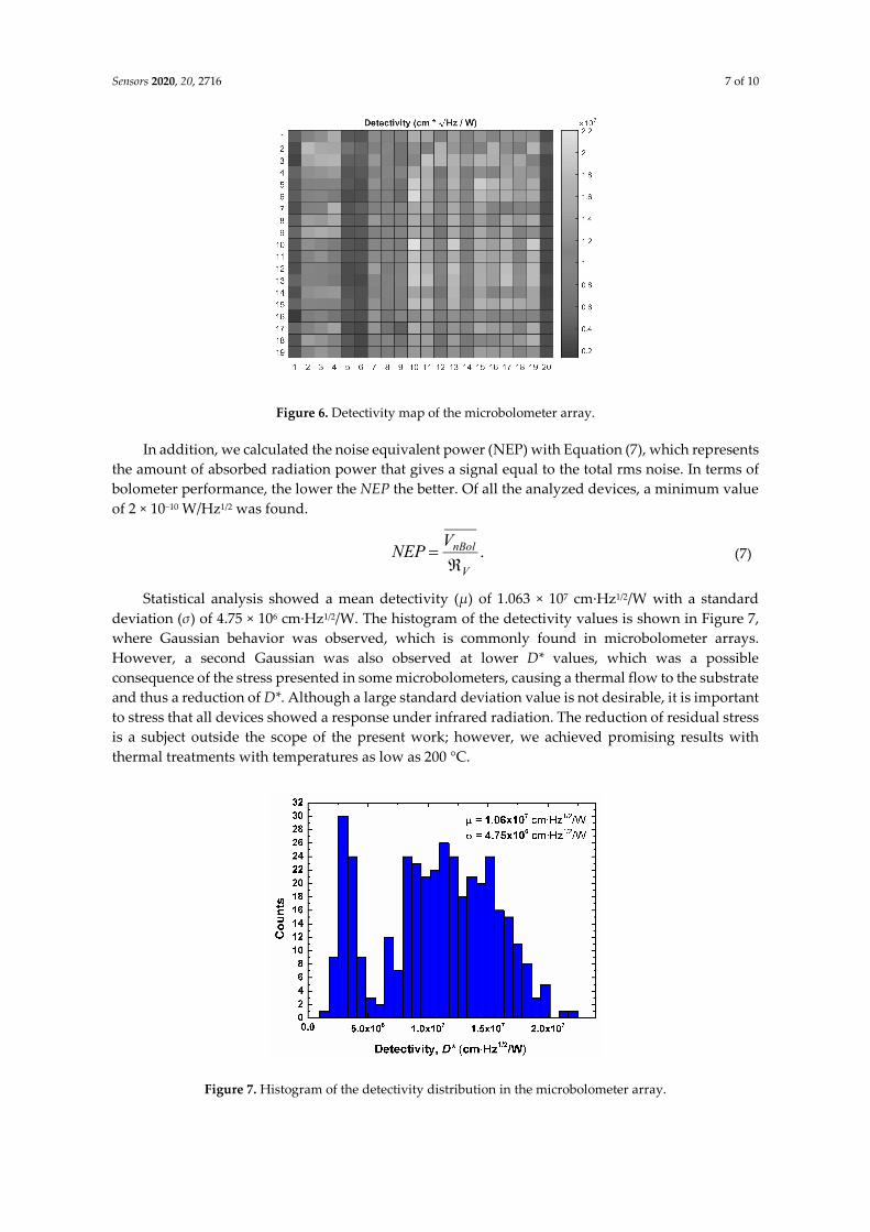
A detectivity map of the 380 measured devices is shown in Figure 6. A maximum D* was found
to be 2 × 107 cm∙Hz1/2/W, while the minimum was approximately 0.2 × 107 cm∙Hz1/2/W. Furthermore,
it was observed that all devices responded to infrared radiation, which is a consequence of the
structural integrity of all the microbolometers in the array. This is of major importance since the
percentage of damaged pixels in a commercial array is in the order of 1% [32]. The performance of
the pm‐SixGe1‐x:H film implemented on a 19 × 20 microbolometer array serves as a proof‐of‐concept
to assess its application on commercial devices. This material is an ideal candidate to reduce
manufacturing cost as it can be readily integrated with CMOS back‐end‐of‐the‐line processes and
ultimately to be applied in detectors of low‐cost and high‐volume markets [33].
Sensors 2020, 20, 2716 7 of 10
Figure 6. Detectivity map of the microbolometer array.
In addition, we calculated the noise equivalent power (NEP) with Equation (7), which represents
the amount of absorbed radiation power that gives a signal equal to the total rms noise. In terms of
bolometer performance, the lower the NEP the better. Of all the analyzed devices, a minimum value
of 2 × 10⁻¹⁰ W/Hz1/2 was found.
.V
nBolVNEP
(7)
Statistical analysis showed a mean detectivity (µ) of 1.063 × 107 cm∙Hz1/2/W with a standard
deviation (σ) of 4.75 × 106 cm∙Hz1/2/W. The histogram of the detectivity values is shown in Figure 7,
where Gaussian behavior was observed, which is commonly found in microbolometer arrays.
However, a second Gaussian was also observed at lower D* values, which was a possible
consequence of the stress presented in some microbolometers, causing a thermal flow to the substrate
and thus a reduction of D*. Although a large standard deviation value is not desirable, it is important
to stress that all devices showed a response under infrared radiation. The reduction of residual stress
is a subject outside the scope of the present work; however, we achieved promising results with
thermal treatments with temperatures as low as 200 °C.
Figure 7. Histogram of the detectivity distribution in the microbolometer array.
Sensors 2020, 20, 2716 8 of 10
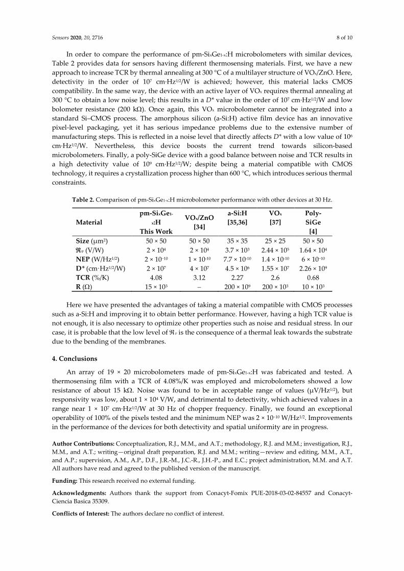
In order to compare the performance of pm‐SixGe1‐x:H microbolometers with similar devices,
Table 2 provides data for sensors having different thermosensing materials. First, we have a new
approach to increase TCR by thermal annealing at 300 °C of a multilayer structure of VOx/ZnO. Here,
detectivity in the order of 107 cm∙Hz1/2/W is achieved; however, this material lacks CMOS
compatibility. In the same way, the device with an active layer of VOx requires thermal annealing at
300 °C to obtain a low noise level; this results in a D* value in the order of 107 cm∙Hz1/2/W and low
bolometer resistance (200 k). Once again, this VOx microbolometer cannot be integrated into a
standard Si–CMOS process. The amorphous silicon (a‐Si:H) active film device has an innovative
pixel‐level packaging, yet it has serious impedance problems due to the extensive number of
manufacturing steps. This is reflected in a noise level that directly affects D* with a low value of 106
cm∙Hz1/2/W. Nevertheless, this device boosts the current trend towards silicon‐based
microbolometers. Finally, a poly‐SiGe device with a good balance between noise and TCR results in
a high detectivity value of 109 cm∙Hz1/2/W; despite being a material compatible with CMOS
technology, it requires a crystallization process higher than 600 °C, which introduces serious thermal
constraints.
Table 2. Comparison of pm‐SixGe1‐x:H microbolometer performance with other devices at 30 Hz.
Material
pm-SixGe1-
x:H
This Work
VOx/ZnO
[34]
a-Si:H
[35,36]
VOx
[37]
Poly-
SiGe
[4]
Size (µm2) 50 × 50 50 × 50 35 × 35 25 × 25 50 × 50
v (V/W) 2 × 10⁴ 2 × 10⁴ 3.7 × 10³ 2.44 × 10⁵ 1.64 × 10⁴
NEP (W/Hz1/2) 2 × 10⁻¹⁰ 1 × 10‐10 7.7 × 10‐10 1.4 × 10‐10 6 × 10⁻¹⁰
D* (cm·Hz1/2/W) 2 × 10⁷ 4 × 10⁷ 4.5 × 10⁶ 1.55 × 10⁷ 2.26 × 10⁹
TCR (%/K) 4.08 3.12 2.27 2.6 0.68
R () 15 × 103 200 × 109 200 × 103 10 × 103
Here we have presented the advantages of taking a material compatible with CMOS processes
such as a‐Si:H and improving it to obtain better performance. However, having a high TCR value is
not enough, it is also necessary to optimize other properties such as noise and residual stress. In our
case, it is probable that the low level of v is the consequence of a thermal leak towards the substrate
due to the bending of the membranes.
4. Conclusions
An array of 19 × 20 microbolometers made of pm‐SixGe1‐x:H was fabricated and tested. A
thermosensing film with a TCR of 4.08%/K was employed and microbolometers showed a low
resistance of about 15 k. Noise was found to be in acceptable range of values (µV/Hz1/2), but
responsivity was low, about 1 × 10⁴ V/W, and detrimental to detectivity, which achieved values in a
range near 1 × 107 cm∙Hz1/2/W at 30 Hz of chopper frequency. Finally, we found an exceptional
operability of 100% of the pixels tested and the minimum NEP was 2 × 10⁻¹⁰ W/Hz1/2. Improvements
in the performance of the devices for both detectivity and spatial uniformity are in progress.
Author Contributions: Conceptualization, R.J., M.M., and A.T.; methodology, R.J. and M.M.; investigation, R.J.,
M.M., and A.T.; writing—original draft preparation, R.J. and M.M.; writing—review and editing, M.M., A.T.,
and A.P.; supervision, A.M., A.P., D.F., J.R.‐M., J.C.‐R., J.H.‐P., and E.C.; project administration, M.M. and A.T.
All authors have read and agreed to the published version of the manuscript.
Funding: This research received no external funding.
Acknowledgments: Authors thank the support from Conacyt‐Fomix PUE‐2018‐03‐02‐84557 and Conacyt‐
Ciencia Basica 35309.
Conflicts of Interest: The authors declare no conflict of interest.
Sensors 2020, 20, 2716 9 of 10
References
1. Narita, K.; Kuribayashi, R.; Altintas, E.; Someya, H.; Tsuda, K.; Ohashi, K.; Tabuchi, T.; Okubo, S.; Imazato,
M.; Komatsubara, S. A plastic‐based bolometer array sensor using carbon nanotubes for low‐cost infrared
imaging devices. Sens. Actuators A Phys. 2013, 195, 142–147, doi:10.1016/j.sna.2013.03.008.
2. Liger, M.; Tai, Y.‐C. A 32*32 Parylene‐pyrolyzed carbon bolometer imager. In Proceedings of the 19th IEEE
International Conference on Micro Electro Mechanical Systems, Istanbul, Turkey, 22–26 January 2006; pp.
106–109.
3. Håkansson, A.; Shahi, M.; Brill, J.W.; Fabiano, S.; Crispin, X. Conducting‐polymer bolometers for low‐cost
IR‐detection systems. Adv. Electron. Mater. 2019, 5, 1–7, doi:10.1002/aelm.201800975.
4. Sedky, S.; Fiorini, P.; Baert, K.; Hermans, L.; Mertens, R. Characterization and optimization of infrared poly
SiGe bolometers. IEEE Trans. Electron Devices 1999, 46, 675–682, doi:10.1109/16.753700.
5. Gray, J.; Çelik‐Butler, Z.; Butler, D. MgO sacrificial layer for micromachining uncooled Y‐Ba‐Cu‐O IR
microbolometers on Si/sub 3/N/sub 4/ bridges. J. Microelectromech. Syst. 1999, 8, 192–199,
doi:10.1109/84.767115.
6. Yoneoka, S.; Liger, M.; Yama, G.; Schuster, R.; Purkl, F.; Provine, J.; Prinz, F.B.; Howe, R.T.; Kenny, T.W.
ALD‐metal uncooled bolometer. In Proceedings of the IEEE 24th International Conference on Micro Electro
Mechanical Systems, Cancun, Mexico, 23–27 January 2011; pp. 676–679.
7. Saxena, R.; Bhan, R.; Rana, P.S.; Vishwakarma, A.; Aggarwal, A.; Khurana, K.; Gupta, S. Study of
performance degradation in Titanium microbolometer IR detectors due to elevated heating. Infrared Phys.
Technol. 2011, 54, 343–352, doi:10.1016/j.infrared.2011.03.001.
8. Tanaka, A.; Matsumoto, S.; Tsukamoto, N.; Itoh, S.; Chiba, K.; Endoh, T.; Nakazato, A.; Okuyama, K.;
Kumazawa, Y.; Hijikawa, M.; et al. Influence of bias heating on a titanium bolometer infrared sensor.
AeroSense 1997, 3061, 198–209, doi:10.1117/12.280339.
9. Tanrikulu, M.Y.; Okyay, A.K.; Yildizak, C.; Akin, T.; Akar, O.; Sarac, A. Single layer microbolometer
detector pixel using ZnO material. Infrared Technol. Appl. 2018, 10624, 1062417, doi:10.1117/12.2302996.
10. Pope, T.D.; Jerominek, H.; Alain, C.; Cayer, F.; Tremblay, B.; Grenier, C.; Topart, P.A.; LeClair, S.; Picard,
F.; Larouche, C.; et al. Commercial and custom 160x120, 256x1, and 512x3 pixel bolometric FPAs. AeroSense
2002, 4721, 64–75, doi:10.1117/12.478862.
11. Li, C.; Skidmore, G.D.; Han, C.J. Uncooled VOx infrared sensor development and application. SPIE Def.
Secur. Sens. 2011, 8012, 80121, doi:10.1117/12.887113.
12. Wang, B.; Lai, J.; Li, H.; Hu, H.; Chen, S. Nanostructured vanadium oxide thin film with high TCR at room
temperature for microbolometer. Infrared Phys. Technol. 2013, 57, 8–13, doi:10.1016/j.infrared.2012.10.006.
13. Riou, O.; Logerais, P.‐O.; Durastanti, J.F. Quantitative study of the temperature dependence of normal
LWIR apparent emissivity. Infrared Phys. Technol. 2013, 60, 244–250, doi:10.1016/j.infrared.2013.05.012.
14. Han, M.‐S.; Kim, D.H.; Ko, H.‐J.; Shin, J.C. A fabrication and characterictics of microbolometer detectors
using VOx/ZnO/VOx multilayer thin film processing. SPIE Def. Secur. 2014, 9070, 90701,
doi:10.1117/12.2049513.
15. Grayli, S.V.; El‐Chami, I.; Bahreyni, B.; Leach, G. Room temperature deposition of highly sensitive
vanadium oxide films for infrared light sensing applications. In Proceedings of the IEEE Sensors, Busan,
South Korea, 1–4 November 2015; pp. 1–4.
16. Gu, D.; Zhou, X.; Guo, R.; Wang, Z.; Jiang, Y. The microstructures and electrical properties of Y‐doped
amorphous vanadium oxide thin films. Infrared Phys. Technol. 2017, 81, 64–68,
doi:10.1016/j.infrared.2016.12.013.
17. Ahmed, A.H.Z.; Tait, R.N.; Oogarah, T.B.; Liu, H.C.; Denhoff, M.W.; Sproule, G.; Graham, M. A surface
micromachined amorphous GexSi1‐xOy bolometer for thermal imaging applications. In Proceedings of the
Photonic Applications in Astronomy, Biomedicine, Imaging, Materials Processing, and Education, Ottawa,
ON, Canada, 26–29 September 2004; Volume 5578, pp. 298–309.
18. Schimert, T.; Brady, J.; Fagan, T.; Taylor, M.; McCardel, W.; Gooch, R.; Ajmera, S.; Hanson, C.; Syllaios, A.J.
Amorphous silicon based large format uncooled FPA microbolometer technology. Infrared Technol. Appl.
2008, 6940, 694023, doi:10.1117/12.784661.
19. Ajmera, S.; Brady, J.; Hanson, C.; Schimert, T.; Syllaios, A.J.; Taylor, M. Performance improvement in
amorphous silicon based uncooled microbolometers through pixel design and materials development.
Infrared Technol. Appl. 2011, 8012, 80121, doi:10.1117/12.884249.
Sensors 2020, 20, 2716 10 of 10
20. Tissot, J.L.; Robert, P.; Crastes, A.; Tinnes, S.; Bercier, E.; Durand, A. Status of uncooled infrared detector
technology at ULIS, France. Def. Sci. J. 2013, 63, 545–549, doi:10.14429/dsj.63.5753.
21. Zhou, T.; Zuo, Y.; Qiu, K.; Zheng, J.; Wang, Q. Potential of Ti doped hydrogenated amorphous Si film with
suitable resistivity and high TCR for microbolometer applications. Vacuum 2015, 119, 30–33,
doi:10.1016/j.vacuum.2015.04.024.
22. Su, J.‐H.; Yeh, W.‐K.; Chang, W.‐T.; Wu, B.‐L.; Lu, J.‐M.; Wang, J.‐H.; Fang, Y.‐K.; Chen, P.‐Y. Temperature
coefficient of resistance related to amorphous silicon/metal contact design of microbolometers. In
Proceedings of the 3rd International Conference on Devices, Circuits and Systems (ICDCS), Coimbatore,
India, 3–5 March 2016; pp. 63–67.
23. Moreno, M.; Torres, A.; Calleja, C.; Lázaro, R.C.A.; Rosales, P.; Kosarev, A.; Jiménez‐Zavala, R. Exploring
the infrared‐sensing properties of polymorphous silicon‐germanium (pm‐SixGey:H) thin films. Can. J. Phys.
2014, 92, 565–569, doi:10.1139/cjp‐2013‐0545.
24. Bronner, W.; Kleider, J.; Brüggemann, R.; Cabarrocas, P.R.I.; Mencaraglia, D.; Mehring, M. Comparison of
transport and defects properties in hydrogenated polymorphous and amorphous silicon. J. Non-Cryst.
Solids 2002, 299, 551–555, doi:10.1016/s0022‐3093(01)01201‐7.
25. Kim, K.; Johnson, E.; Abramov, A.; Cabarrocas, P.R.I. Light induced electrical and macroscopic changes in
hydrogenated polymorphous silicon solar cells. EPJ Photovolt. 2012, 3, 30301, doi:10.1051/epjpv/2012005.
26. Chou, Y.‐P.; Lee, S.‐C. Structural, optical, and electrical properties of hydrogenated amorphous silicon
germanium alloys. J. Appl. Phys. 1998, 83, 4111–4123, doi:10.1063/1.367229.
27. Jiménez‐Zavala, R.; Moreno, M.; Torres, A.; Rosales, P.; Gomez, V.; Carlos, N.; Cabarrocas, P.R.I. Effect of
Pressure and Flow Rates on Polymorphous Silicon‐Germanium (pm‐Six Ge1−x:H) Thin Films for Infrared
Detection Applications. Phys. Status Solidi A 2018, 215, 1700735, doi:10.1002/pssa.201700735.
28. Moreno, M.; Jiménez‐Zavala, R.; Torres, A.; Lázaro, R.C.A. Microbolometers based on amorphous silicon–
germanium films with embedded nanocrystals. IEEE Trans. Electron Devices 2015, 62, 2120–2127,
doi:10.1109/ted.2015.2434275.
29. Jiménez‐Zavala, R.; Moreno, M.; Torres, A.; Rosales, P.; Sanz‐Pascual, M.T.; Lázaro, R.C.A. Performance
characterization of infrared detectors based on polymorphous silicon‐germanium (pm‐Six Ge1−x:H) thin
films deposited at low temperature. Phys. Status Solidi A 2018, 215, 1700736, doi:10.1002/pssa.201700736.
30. Cabarrocas, P.R.I.; Chaâbane, N.; Kharchenko, A.V.; Tchakarov, S. Polymorphous silicon thin films
produced in dusty plasmas: Application to solar cells. Plasma Phys. Control. Fusion 2004, 46, B235–B243,
doi:10.1088/0741‐3335/46/12b/020.
31. Tanielian, M. Adsorbate effects on the electrical conductance of a‐Si: H. Philos. Mag. B 1982, 45, 435–462,
doi:10.1080/01418638208227449.
32. Budzier, H.; Gerlach, G. Calibration of uncooled thermal infrared cameras. J. Sens. Sens. Syst. 2015, 4, 187–
197, doi:10.5194/jsss‐4‐187‐2015.
33. Liddiard, K.C. Application of mosaic pixel microbolometer technology to very high‐performance, low‐cost
thermography and pedestrian detection. SPIE Def. Secur. Sens. 2013, 8704, 87043, doi:10.1117/12.2018593.
34. Han, M.‐S.; Kim, D.H.; Ko, H.J.; Kim, H. Vanadium oxide microbolometer using ZnO sandwich layer. Appl.
Sci. Converg. Technol. 2015, 24, 178–183, doi:10.5757/asct.2015.24.5.178.
35. Ahmed, M.; Butler, D.P.; Celik‐Butler, Z. Device‐level vacuum packaged uncooled microbolometer on a
polyimide substrate. Infrared Phys. Technol. 2016, 79, 50–57, doi:10.1016/j.infrared.2016.09.011.
36. Ahmed, M.; Chitteboyina, M.M.; Butler, D.P.; Celik‐Butler, Z. Temperature sensor in a flexible substrate.
IEEE Sens. J. 2011, 12, 864–869, doi:10.1109/jsen.2011.2166064.
37. Abdel‐Rahman, M.; Al‐Khalli, N.; Zia, M.F.; Alduraibi, M.; Ilahi, B.; Debbar, N.; Awad, E. Fabrication and
design of vanadium oxide microbolometer. In Proceedings of the 6th International Advances in Applied
Physics and Materials Science Congress & Exhibition, Istanbul, Turkey, 1–3 June, 2016; Volume 1809, p.
20001.
© 2020 by the authors. Licensee MDPI, Basel, Switzerland. This article is an open access
article distributed under the terms and conditions of the Creative Commons Attribution
(CC BY) license (http://creativecommons.org/licenses/by/4.0/).
Related Documents