Lucent Technologies Proprietary New Jersey Nanotechnology New Jersey Nanotechnology Consortium Consortium 1 Fabrication of MEMS Devices: Fundamentals and State of the Art Bill Mansfield New Jersey Nanotechnology Consortium www.njnc.com Bell Labs Lucent Technology [email protected]

Welcome message from author
This document is posted to help you gain knowledge. Please leave a comment to let me know what you think about it! Share it to your friends and learn new things together.
Transcript

Lucent Technologies Proprietary
New Jersey Nanotechnology New Jersey Nanotechnology ConsortiumConsortium
1
Fabrication of MEMS Devices:Fundamentals and State of the Art
Bill MansfieldNew Jersey Nanotechnology Consortiumwww.njnc.comBell LabsLucent [email protected]

Lucent Technologies Proprietary
New Jersey Nanotechnology New Jersey Nanotechnology ConsortiumConsortium
2
OUTLINE
I. MEMS Basics
II. MEMS Fabrication Fundamentals
III. MEMS Fabrication Processes and ExamplesA. Bulk Micro-machining Processes
1. Non silicon based HAR
2. Silicon based
B. Hybrid Processes
C. Surface Micro-machining Processes
D. Soft MEMS Processes

Lucent Technologies Proprietary
New Jersey Nanotechnology New Jersey Nanotechnology ConsortiumConsortium
3
Micro and Nano Machines:Many Different Types of Motion

Lucent Technologies Proprietary
New Jersey Nanotechnology New Jersey Nanotechnology ConsortiumConsortium
4
Motion Actuation Methods
VoltageNeeds
SwitchingSpeed
Currentconsumption
Electrostatic High High Low (none)
Magnetic Low High High
Thermal Low Slow high
Others: piezoelectric, stress relaxation, surface tension, …...

Lucent Technologies Proprietary
New Jersey Nanotechnology New Jersey Nanotechnology ConsortiumConsortium
5
MEMS and NEMS: In-plane motion
20 µm
V
Electrostatic actuation

Lucent Technologies Proprietary
New Jersey Nanotechnology New Jersey Nanotechnology ConsortiumConsortium
6

Lucent Technologies Proprietary
New Jersey Nanotechnology New Jersey Nanotechnology ConsortiumConsortium
7
1. Film Deposition
2. Lithography
3. Pattern transfer
4. Cleaning
5. Metrology
6. Chemical Mechanical Polishing
7. Structure release
MEMS FABRICATION BASICS
Lucent Technologies Proprietary
New Jersey Nanotechnology New Jersey Nanotechnology ConsortiumConsortium
8
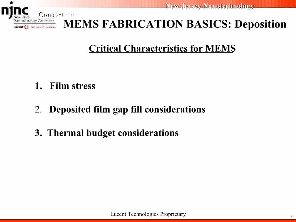
MEMS FABRICATION BASICS: Deposition
1. Film stress
2. Deposited film gap fill considerations
3. Thermal budget considerations
Critical Characteristics for MEMS

Lucent Technologies Proprietary
New Jersey Nanotechnology New Jersey Nanotechnology ConsortiumConsortium
9
500 600 700 800 900 1000 1100
-300
-200
-100
0
100
200
580oC
615oC
550oC
Stre
ss (
MPa
)
Annealing Temperature (oC)
Controlling Stress in a single layer of poly-Si: Thermal annealing
Annealing in N2 at 1050c for 2 hours will reduce the stress to <5MPa/um

Lucent Technologies Proprietary
New Jersey Nanotechnology New Jersey Nanotechnology ConsortiumConsortium
10
Controlling Stress and Gradient Stress with multilayer design
Compressive
Compressive
Compressive
Tensile
Tensile
Out-of-plane Stress gradient ~ 2 Mpa/um can be reached.No annealing is needed. This also allows structural design to be customized to compressive or tensile and by varying
the layer thickness, a desired stress can be achieved.

Lucent Technologies Proprietary
New Jersey Nanotechnology New Jersey Nanotechnology ConsortiumConsortium
11
Film stress pattern and process dependencies

Lucent Technologies Proprietary
New Jersey Nanotechnology New Jersey Nanotechnology ConsortiumConsortium
12
Gap Fill Considerations
Greater thesurface mobilityof deposited atomsbetter the fill.
11111111111

Lucent Technologies Proprietary
New Jersey Nanotechnology New Jersey Nanotechnology ConsortiumConsortium
13
MEMS FABRICATION BASICS: Lithography
1. Wafer flatness – thick stressed films distort wafers resulting in loading and chucking problems.2. Depth of focus – thick films result in extreme topo- graphy over which fine feature resolution cannot be maintained.3. Level to level alignment – thick films can result in attenuated or no alignment mark signal compromising alignment capability.4. Resist material etch selectivity- resist materials for advanced lithography are designed for thin films pattern transfer and may not have sufficient selectivity for dry etch pattern transfer to thick films.
Critical Issues for MEMS

Lucent Technologies Proprietary
New Jersey Nanotechnology New Jersey Nanotechnology ConsortiumConsortium
14
0.25 um wide, 12um deep fingers, about a factor of 3 more than our initial design target in both width and depth.
Vertical Comb Drive Etch Process
MEMS FABRICATION BASICS: Pattern Transfer

Lucent Technologies Proprietary
New Jersey Nanotechnology New Jersey Nanotechnology ConsortiumConsortium
15
MEMS FABRICATION BASICS: Pattern Transfer
High Aspect Ratio (HAR) Deep Silicon Etching
50um wide features etched 250um deepwith standard Bosch process
50um wide features etched 240um deepwith modified Bosch process
Bosch process: deposition/etch alternationC4F8 deposition precursor / silicon etch SF6 and O2.

Lucent Technologies Proprietary
New Jersey Nanotechnology New Jersey Nanotechnology ConsortiumConsortium
16
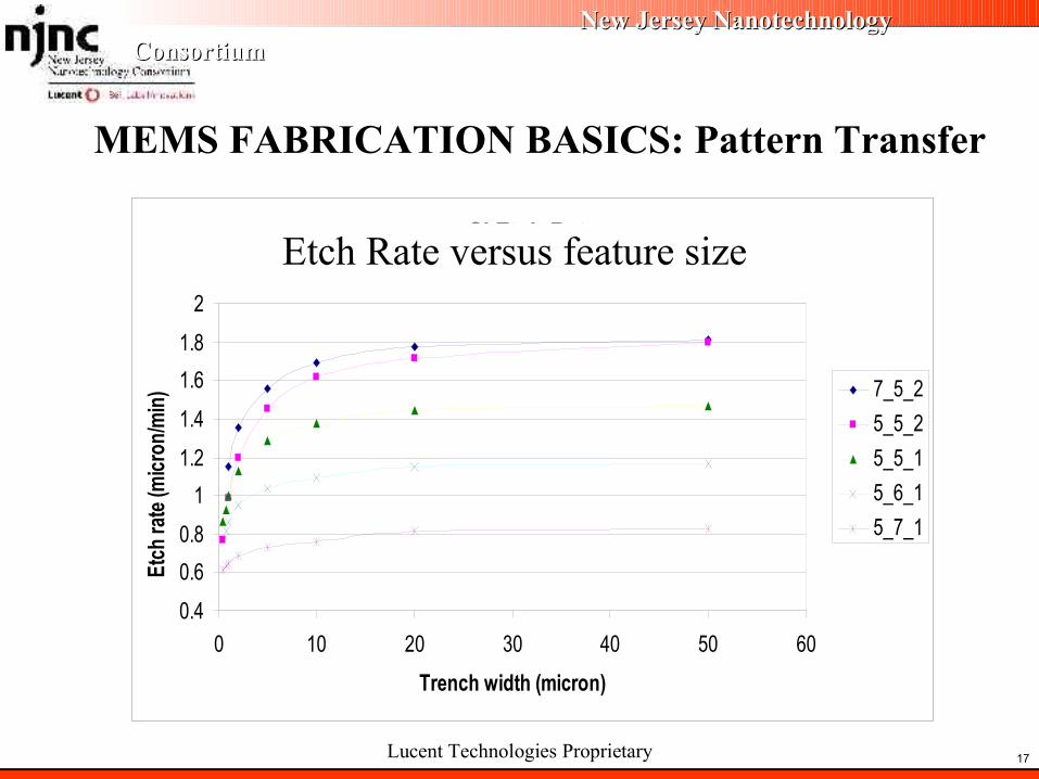
MEMS FABRICATION BASICS: Pattern Transfer
1. Etch Rate versus feature size2. Profile control-angle and texture3. Etch mask and etch stop layers4. Etch rate versus area considerations (loading)5. Etch uniformity
Lucent Technologies Proprietary
New Jersey Nanotechnology New Jersey Nanotechnology ConsortiumConsortium
17
Si Etch Rate
0.4
0.6
0.8
1
1.2
1.4
1.6
1.8
2
0 10 20 30 40 50 60
Trench width (micron)
Etch
rate
(mic
ron/
min
) 7_5_2
5_5_2
5_5_1
5_6_1
5_7_1
MEMS FABRICATION BASICS: Pattern Transfer
Etch Rate versus feature size

Lucent Technologies Proprietary
New Jersey Nanotechnology New Jersey Nanotechnology ConsortiumConsortium
18
Side Wall Profile
89.3
89.4
89.5
89.6
89.7
89.8
89.9
90
90.1
90.2
90.3
90.4
0 2 4 6 8 10 12
Trench width (micron)
Sid
e w
all
an
gle
(d
eg
)
7_5_2
5_5_2
5_5_1
5_6_1
5_7_1
Profile control
MEMS FABRICATION BASICS: Pattern Transfer

Lucent Technologies Proprietary
New Jersey Nanotechnology New Jersey Nanotechnology ConsortiumConsortium
19
substrate
Etch stoplayer
Etched features
Etch mask
Etch uniformity, etch stop layers, loading, and etch mask layers
MEMS FABRICATION BASICS: Pattern Transfer
Feature undercut
Etch residues

Lucent Technologies Proprietary
New Jersey Nanotechnology New Jersey Nanotechnology ConsortiumConsortium
20
MEMS FABRICATION BASICS: Pattern Transfer
Silicon sidewall – Bosch etch with resist etch mask

Lucent Technologies Proprietary
New Jersey Nanotechnology New Jersey Nanotechnology ConsortiumConsortium
Silicon Substrate
Nitride
Poly 0
1st Oxide
Poly 1
2nd Oxide
Poly 2
Metal
Multi-User MEMS Processes (MUMPS) Introduction and Design Rules, rev. 4, 7/15/96, MCNC MEMS Technology Applications Center, Research Triangle Park, NC 27709
0.6 µm Si nitride
0.5 µm Si
2 µm PSG
2 µm Si
0.75 µm PSG
1.5 µm Si 0.5 µm Au, on Cr adhesion layer
SurfaceMicromachiningProcess
MEMS FABRICATION BASICS: Chemical Mechanical Polishing
Lucent Technologies Proprietary
New Jersey Nanotechnology New Jersey Nanotechnology ConsortiumConsortium
22
Chemical Mechanical Polishing
Side View Top View
Slurry Feed
Carrier
Holder
Wafer
Platen
Polishing Pad
Slurry
z = oxide topographyt = polish timep = pressurev = velocityρ(x,y,z) = pattern density
KP = Preston constant
K = Constant
Oxide 2 zPad
Slurry

Lucent Technologies Proprietary
New Jersey Nanotechnology New Jersey Nanotechnology ConsortiumConsortium
23
Patten Density EffectsAs Deposited Topography
Oxide 2
Oxide 1
Metal
Dummy Fill Pattern
Oxide 2
Oxide 1
Metal
CMP: Global PlanarityOxide 2
Oxide 1
Metal
CMP: Local Planarity
Oxide 2
Oxide 1
Metal
Reverse Tone: Litho
Oxide 2
Oxide 1
Metal
Resist
Reverse Tone: Etch
Oxide 2
Oxide 1
Metal
CMP: Global PlanarityOxide 2
Oxide 1
Metal
Global Non-Planarity

Lucent Technologies Proprietary
New Jersey Nanotechnology New Jersey Nanotechnology ConsortiumConsortium
24
Layers of structural materials, sacrificial layers, and interconnects or electrodes are deposited and patterned.
The sacrificial layers are selectively removed, releasing the moving parts.
Some micromachines self-assemble during release.
MEMS FABRICATION BASICS: Release

Lucent Technologies Proprietary
New Jersey Nanotechnology New Jersey Nanotechnology ConsortiumConsortium
25
MEMS FABRICATION BASICS: Release
Post wet release processing usually entails rinse with DI waterthen solvent or critical CO2 dry.
* Will not attack Aluminum metallization
Structural Material Sacrificial Material Release Agent
silicon silicon dioxide Aqueos HFsilicon/germanium HF Gas
PAD Etch*
protected silicon silicon Xenon difluoride gas*
silicon/germanium germanium Hydrogen peroxide*
Germanium silicon dioxide Aqueos HFHF Gas

Lucent Technologies Proprietary
New Jersey Nanotechnology New Jersey Nanotechnology ConsortiumConsortium
26
Stiction after release No stiction
MEMS FABRICATION BASICS: Release

Lucent Technologies Proprietary
New Jersey Nanotechnology New Jersey Nanotechnology ConsortiumConsortium
27
BULK MICROMACHINING:Non-silicon High Aspect Ratio(HAR) MEMS

Lucent Technologies Proprietary
New Jersey Nanotechnology New Jersey Nanotechnology ConsortiumConsortium
28
LIGA Nickel High Aspect Ratio (HAR) Micromachining(Lithographie, Galvanoformung, Abformung (LIGA))
1. Electroplate into moldand remove mold material.–
X-Ray Radiation
PMMA
Gold Mask
2. Develop PMMA into mold1. Expose PMMA to Synchrotron radiation
Feature lengths and widths as small as 20um
Feature heights are from 200-300um
Aspect Ratios > 10
E. W. Becker etal., ),” Microelectron.Eng., vol. 4, pp. 35–36, 1986.

Lucent Technologies Proprietary
New Jersey Nanotechnology New Jersey Nanotechnology ConsortiumConsortium
29
Optical absorption of SU-8 (A) as compared to a diazo type resist system (B) and Dupont RISTON dry film (C)
* Reference: N. LaBianca, and J. Delorme, "High aspect ratio resist for thick film applications", in Proc. SPIE vol. 2438, SPIE, (1995)
22umgap,24um line feature Profiles in 290xm thick SU-8 film with non-
optimized process.
UV-LIGA High Aspect Ratio (HAR) Micro-machining

Lucent Technologies Proprietary
New Jersey Nanotechnology New Jersey Nanotechnology ConsortiumConsortium
30
BULK MICROMACHINING: Silicon Dry Etch Based
Bulk machined parts in 300um silicon using
Modified Bosch process.

Lucent Technologies Proprietary
New Jersey Nanotechnology New Jersey Nanotechnology ConsortiumConsortium
31
Lucent Lambda Router Mirrors ( Bishop etal.)
BULK MICROMACHINING: SOI

Lucent Technologies Proprietary
New Jersey Nanotechnology New Jersey Nanotechnology ConsortiumConsortium
32
Pattern Front-side of SOI ( Silicon on Insulator) wafer with Mirror Array Pattern:
High Throughput, High Resolution, High alignment precision step and repeat exposure tool
Siliconoxide
Silicon
Hard Mask MaterialThin resist
BULK MICROMACHINING

Lucent Technologies Proprietary
New Jersey Nanotechnology New Jersey Nanotechnology ConsortiumConsortium
33
Pattern Transfer Resist Pattern into Hard Mask Material with Dry Etch
Strip and clean residual resist
Siliconoxide
Silicon
BULK MICROMACHINING

Lucent Technologies Proprietary
New Jersey Nanotechnology New Jersey Nanotechnology ConsortiumConsortium
34
Pattern Transfer Resist Pattern into Hard Mask Material with Dry Etch
Strip and clean residual resist
Siliconoxide
Silicon
BULK MICROMACHINING
Lucent Technologies Proprietary
New Jersey Nanotechnology New Jersey Nanotechnology ConsortiumConsortium
35
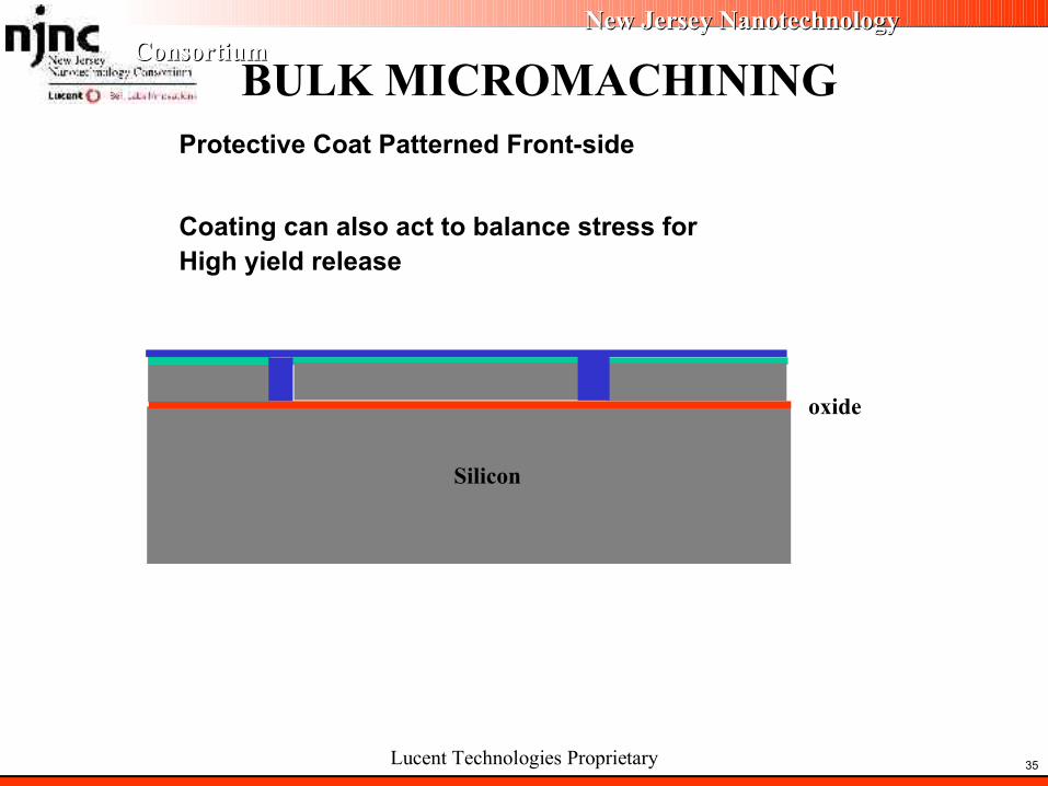
Protective Coat Patterned Front-side
Coating can also act to balance stress forHigh yield release
Siliconoxide
Silicon
BULK MICROMACHINING

Lucent Technologies Proprietary
New Jersey Nanotechnology New Jersey Nanotechnology ConsortiumConsortium
36
Handle wafer thinning
Wafer wet cleaning
Backside lithography with contact printer
oxide
Silicon
Silicon
BULK MICROMACHINING

Lucent Technologies Proprietary
New Jersey Nanotechnology New Jersey Nanotechnology ConsortiumConsortium
37
Backside Cavity Deep Reactive Ion Etch
oxide
Silicon
Silicon
BULK MICROMACHINING

Lucent Technologies Proprietary
New Jersey Nanotechnology New Jersey Nanotechnology ConsortiumConsortium
38
Backside resist strip and clean
Wafer wet release in HF
Mirror Coat at Chip Scale
oxide
Silicon
Silicon
BULK MICROMACHINING
Lucent Technologies Proprietary
New Jersey Nanotechnology New Jersey Nanotechnology ConsortiumConsortium
39
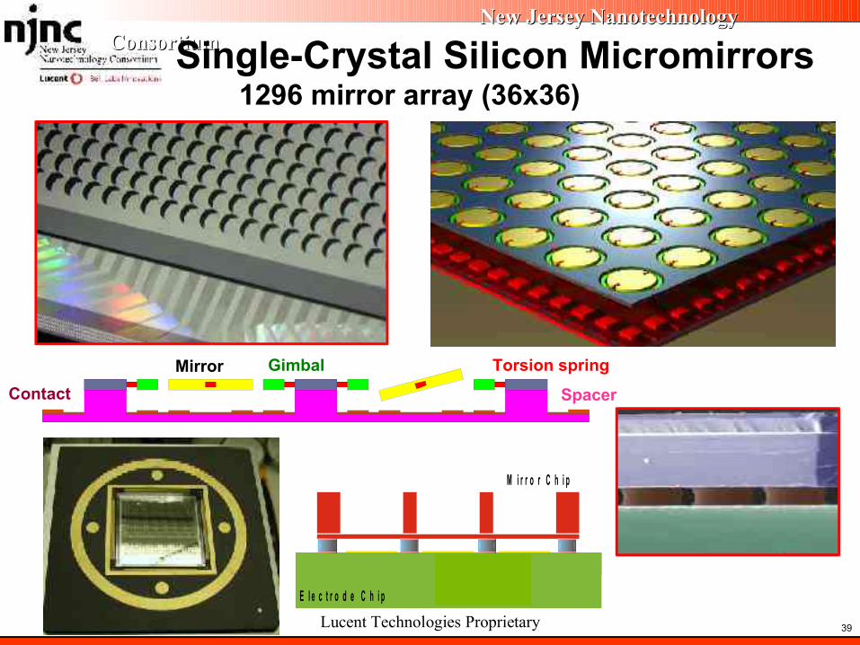
Mirror Gimbal Torsion spring
SpacerContact
Single-Crystal Silicon Micromirrors1296 mirror array (36x36)
E l e c t r o d e C h i p
M i r r o r C h i p
s o l d e r b u m p s

Lucent Technologies Proprietary
New Jersey Nanotechnology New Jersey Nanotechnology ConsortiumConsortium
40
HYBRID MICROMACHININGPROCESS AND EXAMPLE

Lucent Technologies Proprietary
New Jersey Nanotechnology New Jersey Nanotechnology ConsortiumConsortium
41
Monolithic Fringing-Field 1xN Switch
Greywall, Pai etal.Bell LabsNJNCLucent Technology.
Mirror
Electrode
springs

Lucent Technologies Proprietary
New Jersey Nanotechnology New Jersey Nanotechnology ConsortiumConsortium
42
SOI wafer: Si on 0.4 um buried oxide on substrate
SOI Lithography: Pattern resist on hard-mask 0.4 um/0.4 um L/S with DUV step and repeat system.
SOI Etch: etch hard-mask, resist strip & clean, Si etch.
Monolithic Fringing Field Process

Lucent Technologies Proprietary
New Jersey Nanotechnology New Jersey Nanotechnology ConsortiumConsortium
43
Plasma enhanced Dielectric Deposition:
PETEOS/PE-BPTEOSTotal Thickness = 0.7um
Dielectric flow: 1000 C 1 min N2
W1 Lithography with DUV step and repeat system: 5 um contact size
Photo resist dispense optimized for topography coverage
W1 Etch: contacts to SOI and substrate, plasma strip resist and wet clean wafers
Monolithic Fringing Field Process

Lucent Technologies Proprietary
New Jersey Nanotechnology New Jersey Nanotechnology ConsortiumConsortium
44
Poly 1 Deposition: 10 um Boron doped *0.1-0.2 ohm-cm
Align mark open:
1. PR mask lithography, and etch.
Monolithic Fringing Field Process

Lucent Technologies Proprietary
New Jersey Nanotechnology New Jersey Nanotechnology ConsortiumConsortium
45
Poly1 Lithography:
3 um/3 um L/S
Poly 1 Etch: etch 10 um poly, stopping on oxide
Monolithic Fringing Field Process
Lucent Technologies Proprietary
New Jersey Nanotechnology New Jersey Nanotechnology ConsortiumConsortium
46
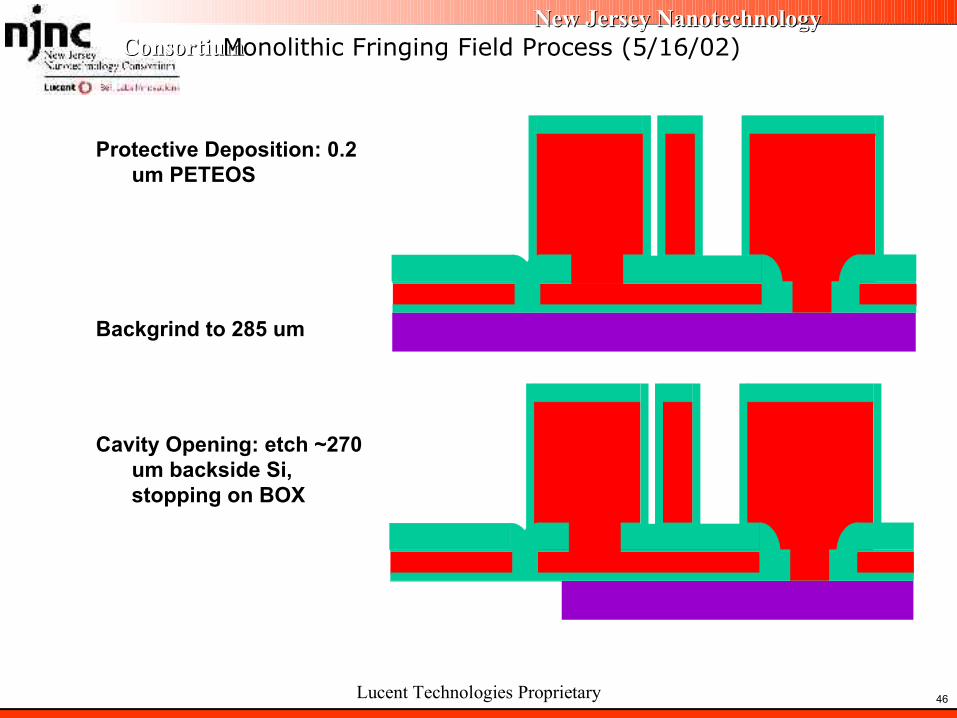
Protective Deposition: 0.2 um PETEOS
Backgrind to 285 um
Cavity Opening: etch ~270 um backside Si, stopping on BOX
Monolithic Fringing Field Process (5/16/02)

Lucent Technologies Proprietary
New Jersey Nanotechnology New Jersey Nanotechnology ConsortiumConsortium
47
Full Wafer Release:
HF 10:1 40 min
Scribe & Break
Al Metalization: 500A mirror front & back, 6000A bond pads
Monolithic Fringing Field Process (5/16/02)

Lucent Technologies Proprietary
New Jersey Nanotechnology New Jersey Nanotechnology ConsortiumConsortium
48
SURFACE MICROMACHINING

Lucent Technologies Proprietary
New Jersey Nanotechnology New Jersey Nanotechnology ConsortiumConsortium
49
Surface Micromachining
Material Systems:High Temperature: poly-silicon structural and conductor, silicon dioxide sacrificial
layer. Wet and dry release systems available.
Low Temperature: poly-silicon germaniun structural and conductor,germanium sacrificial. To date , wet release systems only.
Advantages:Single side processing eliminates need for special tools and chucking.
Single side processing opens door to foundry fabrication.
Can be scaled to sub-micron using already available tools with some exceptions.
Holds possibility (low temp) for modular integration with optimized CMOS.
Disadvantages:New low temperature materials and fabrication processes must be developed and
optimized.
Lucent Technologies Proprietary
New Jersey Nanotechnology New Jersey Nanotechnology ConsortiumConsortium
50
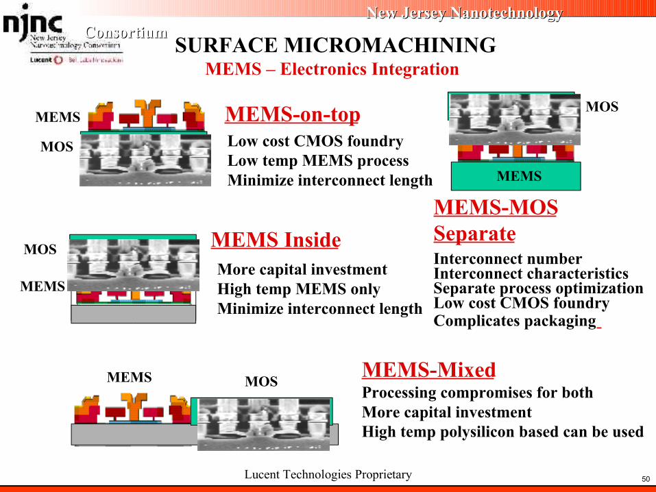
MOS
MOS
MOS
MOS
MEMS Inside
MEMS-on-top
MEMS-MixedProcessing compromises for bothMore capital investmentHigh temp polysilicon based can be used
SURFACE MICROMACHININGMEMS – Electronics Integration
MOS
MEMS-MOSSeparateInterconnect numberInterconnect characteristicsSeparate process optimizationLow cost CMOS foundryComplicates packaging
MEMS
MEMS
MEMS
MEMS
Low cost CMOS foundryLow temp MEMS processMinimize interconnect length
More capital investmentHigh temp MEMS onlyMinimize interconnect length

Lucent Technologies Proprietary
New Jersey Nanotechnology New Jersey Nanotechnology ConsortiumConsortium
51
SOFT MEMS: Position and Shape control of small droplets of condensed matter through surface patterning and electro-
wetting
Tom Krupenkin, Ashley Taylor,
Tobias Schneider,
Shu Yang, Avi Kornblit
Bell Labs, NJNC Lucent Tech.

Lucent Technologies Proprietary
New Jersey Nanotechnology New Jersey Nanotechnology ConsortiumConsortium
52
Contact angle
Contact angle θ is determined
by the interfacial tensions γ:
solid
liquid
Surface tension dominates
d ~ 10 1 - 10 3 µm
Definition of the contactDefinition of the contact angle angle θθ
θ
d
cosθ =γ Solid-Vapor−γ Solid-Liquid
γ Liquid-Vapor

Lucent Technologies Proprietary
New Jersey Nanotechnology New Jersey Nanotechnology ConsortiumConsortium
53
Liquids on nanostructured surfaces
liquid
solid
θ0liquid
solid
Superhydrophobic Wetting
θ0 >> 90° θ0 << 90°
• Surface tension adjustment• Electrowetting

Lucent Technologies Proprietary
New Jersey Nanotechnology New Jersey Nanotechnology ConsortiumConsortium
54
Nanostructured surfacesTypical examples of the structures currently available for usTypical examples of the structures currently available for us
liquid
solid
cosθ =γ Solid-Vapor−γ Soid-Liquid
γ Liquid-Vapor
γ Solid-Liquid= f γ S-L 1− f γ L-V
A 1 A 2
f = A1 / A2Eric Mazur et. al (Harvard, 2001) Cassie & Baxter (1944)
3 µm 3 µm3 µm
3.75 µm 4 µm
Ashley Taylor (NJNC, 2002)
Ashley Taylor (NJNC, 2002)
Lucent Technologies Proprietary
New Jersey Nanotechnology New Jersey Nanotechnology ConsortiumConsortium
55
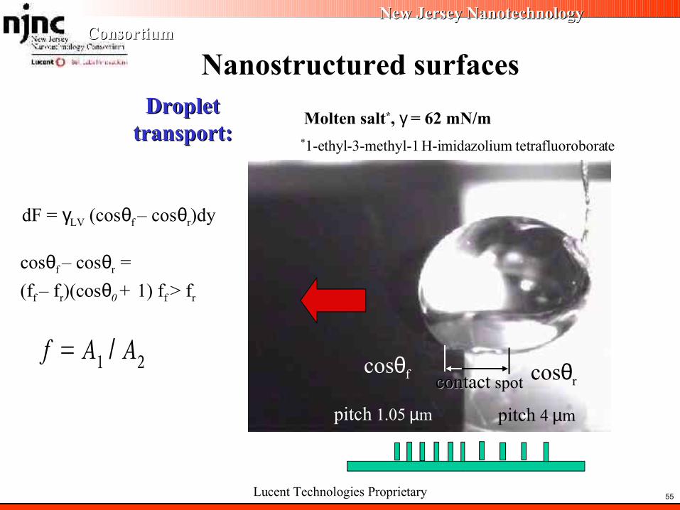
Nanostructured surfacesDroplet Droplet
transport:transport:Molten salt*, γ = 62 mN/m
*1-ethyl-3-methyl-1 H-imidazolium tetrafluoroborate
pitch 1.05 µm pitch 4 µm
contactcontact spot spotcosθf cosθr
dF = γLV (cosθf – cosθr)dy
cosθf – cosθr =
(ff – fr)(cosθ0 + 1) ff
> fr
f = A1 / A2

Lucent Technologies Proprietary
New Jersey Nanotechnology New Jersey Nanotechnology ConsortiumConsortium
56
d=1 mμ
d=0.1 mμd=0.5 mμ
Electrowetting
cosθ V =cosθ V=0 ε 0 ε r
2dγ LV 2
θθ can be reversibly changed using electrowettingcan be reversibly changed using electrowetting
conducting liquid
V γ L
θ
conductive electrode
insulating layer, thickness d,dielectric constant ε r
d
Example: Water droplet on Cytop® surface
ε r=2. 1γ L=72 mN/m
θ V=0=112°
θ [º]
V [V ]

Lucent Technologies Proprietary
New Jersey Nanotechnology New Jersey Nanotechnology ConsortiumConsortium
57
Nanostructured surfacesElectrowettingElectrowetting
conductor
isolator
f2
f1
f2 >> f1
cosθ ~ f
potentially strongly nonlinear effectcontact angle controlcontact angle hysteresis controlpotentially very low voltage
V = 0
V ≠ 0
low-energycoating

Lucent Technologies Proprietary
New Jersey Nanotechnology New Jersey Nanotechnology ConsortiumConsortium
58
Nanostructured surfacesMicroscopic pictureMicroscopic picture
sticky droplet electrowetted droplet
no penetration complete penetration
rolling ball
complete penetration

Lucent Technologies Proprietary
New Jersey Nanotechnology New Jersey Nanotechnology ConsortiumConsortium
59
Electrically induced transitions
Rolling ball - Sticky droplet transitionRolling ball - Sticky droplet transitionco
sθ
cosθ
-1.0
-0.8
-0.6
-0.4
-0.2
0
0.8
0.6
0.4
0.2
1000 2000 30000
Voltage Squared (V2)
(pla
nar
)
(nan
ost
ruct
ure
d)
pitch 4.0 µm
pitch 1.05 µm
planar substrate

Lucent Technologies Proprietary
New Jersey Nanotechnology New Jersey Nanotechnology ConsortiumConsortium
60
Other Applications
Optics, bio-inspired optics
Controllable transport networks
Chemical and bio-sensors
ε2
ε1
λ1 λ2
Dynamic wavelength selective filters
Lucent Technologies Proprietary
New Jersey Nanotechnology New Jersey Nanotechnology ConsortiumConsortium
61
Acknowlegements:
D.J. BishopJ.V. GatesT. CraddockS. RossD.M. TennantR. CirelliL. FetterS. PauP. WatsonE. BowerE. FerryW. Y-C. LaiD. LopezC.S. PaiT. Sorsch
S. ArneyH. SheaV.K. AksyukC.A. BolleD. GreywallF. PardoM. SimonB. FrahmA. GasparyanR. Papazian
NJNC Staff and Management

Lucent Technologies Proprietary
New Jersey Nanotechnology New Jersey Nanotechnology ConsortiumConsortium
62
MEMS FABRICATION BASICS: Deposition
Currently available materials ( polysilicon and single crystalSilicon) are either not possible at low temperatures.(<600C) or cannot be made low stress at low temperature. Low temperature, low stress materials such as poly Si-Ge are currently being developed but they have not been rigorously tested for reliability for long term reliability.
Critical Issues for MEMS
Lucent Technologies Proprietary
New Jersey Nanotechnology New Jersey Nanotechnology ConsortiumConsortium
63
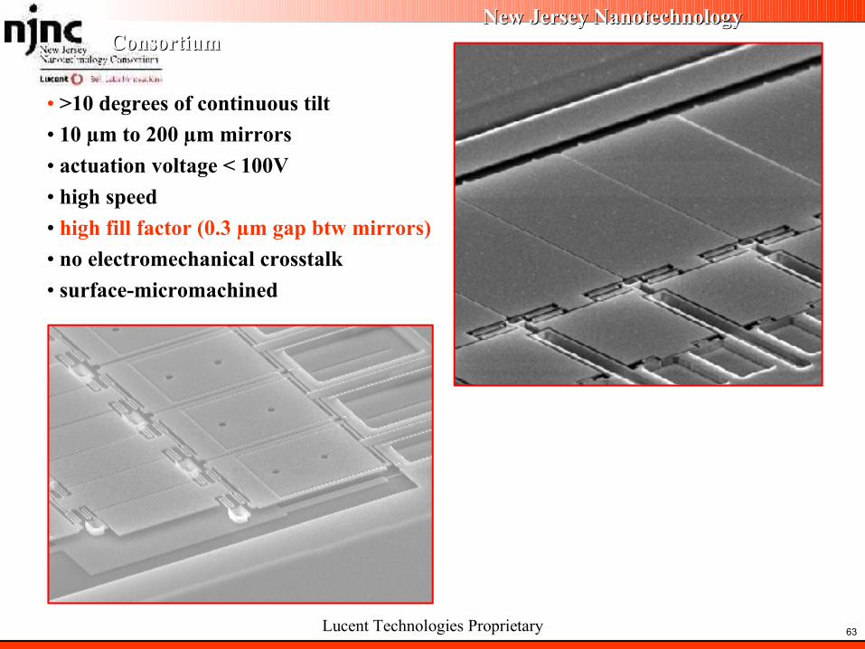
• >10 degrees of continuous tilt
• 10 µm to 200 µm mirrors
• actuation voltage < 100V
• high speed
• high fill factor (0.3 µm gap btw mirrors)
• no electromechanical crosstalk
• surface-micromachined

Lucent Technologies Proprietary
New Jersey Nanotechnology New Jersey Nanotechnology ConsortiumConsortium
64

Lucent Technologies Proprietary
New Jersey Nanotechnology New Jersey Nanotechnology ConsortiumConsortium
65
Angle amplification
The transmission mechanism increases work produced by the actuator:• larger area can be used
• actuator gap can be decreased,
while maintaining the required range of motion

Lucent Technologies Proprietary
New Jersey Nanotechnology New Jersey Nanotechnology ConsortiumConsortium
66
PolySilicon 0.5um
PolySilicon 1.0um
Mirror Metal 0.04um
Si-Rich Nitride 0.5um
Pad Metal 0.6um
Sacrificial Si Oxide 4.0um
Process Flow

Lucent Technologies Proprietary
New Jersey Nanotechnology New Jersey Nanotechnology ConsortiumConsortium
67
BULK MICROMACHINING:

Lucent Technologies Proprietary
New Jersey Nanotechnology New Jersey Nanotechnology ConsortiumConsortium
68
Overview
Superhydrophobic microfabricated surfaces
+
Electrowetting
Control droplet movement and
wetting

Lucent Technologies Proprietary
New Jersey Nanotechnology New Jersey Nanotechnology ConsortiumConsortium
69
Si Wafer
Oxide-protected PolySi
XeF2 Etch
Si Wafer
HF Etch
Active Membrane
Grid
Dry Release of Protected Silicon Structures

Lucent Technologies Proprietary
New Jersey Nanotechnology New Jersey Nanotechnology ConsortiumConsortium
70
Superhydrophobic SurfacesMobilityMobility
Joonwon Kim & “CJ” Kim (UCLA, 2002)
Sin
(α)
Droplet volume (m3)

Lucent Technologies Proprietary
New Jersey Nanotechnology New Jersey Nanotechnology ConsortiumConsortium
71
High mobility and super-repellency based
tunable microfluidic mixerno slip complete slip
V V
Applications: Micro and Nano-fluidics
3 µm 3 µm3 µmLiquid- solidcontact angle

Lucent Technologies Proprietary
New Jersey Nanotechnology New Jersey Nanotechnology ConsortiumConsortium
72
STRESS RELIEF BORDER
No Border 100um Border-100um space
Lucent Technologies Proprietary
New Jersey Nanotechnology New Jersey Nanotechnology ConsortiumConsortium
73
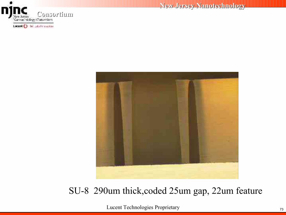
SU-8 290um thick,coded 25um gap, 22um feature

Lucent Technologies Proprietary
New Jersey Nanotechnology New Jersey Nanotechnology ConsortiumConsortium
74
Droplet Movement
• Electrostatic cosθf – cosθr = K(Vf
2 – Vr2) Vf
2> Vr2
•Area density cosθf – cosθr = (ff
– fr)(cosθ0 + 1) ff > fr
cosθrcosθf
dF = γLV (cosθf – cosθr)dy
f = A1 / A2

Lucent Technologies Proprietary
New Jersey Nanotechnology New Jersey Nanotechnology ConsortiumConsortium
75
MEMS FABRICATION
Premise: as with semiconductor fabrication the need for increasing functionality of MEMS devices in time will lead to a need for more, smaller components on individual devices. This in turn will necessitate the need for advanced fabrication equipment and processes and integration of control electronics and MEMS on a single substrate.
Related Documents