Republic of Iraq Ministry of Higher Education and Scientific Research University of Baghdad College of Science Fabrication and study of SnO2 UV-Photodetector A Thesis Submitted to the Comittee of College of Science, University of Baghdad in partial Fulfillment of the Requirements for the Degree of Master of Science in Physics By Azhar Shaker Norry (B.Sc. in Physics 1994) Supervised by Prof. Dr. Abdulla M. Suhail Let. Dr. Asama N. Naje 2014 AD 1435 AH

Welcome message from author
This document is posted to help you gain knowledge. Please leave a comment to let me know what you think about it! Share it to your friends and learn new things together.
Transcript

Republic of Iraq
Ministry of Higher Education
and Scientific Research
University of Baghdad
College of Science
Fabrication and study of SnOR2R UV-Photodetector
A Thesis
Submitted to the Comittee of College of Science, University of Baghdad
in partial Fulfillment of the Requirements for the Degree of
Master of Science in Physics
By
Azhar Shaker Norry (B.Sc. in Physics 1994)
Supervised by
Prof. Dr. Abdulla M. Suhail
LLeett.. DDrr.. Asama N. Naje
2014 AD 1435 AH

بسم هللا الرحمن الرحيم
وح ويسألونك وح قل الر عن الر
من أمر ربي وما أوتيتم من
العلم إال قليال
صدق هللا العظيم
سورة األسراء
۸٥األية

Supervisor Certification
we certify that this thesis was prepared by Miss Azhar Shaker Norry under my supervision at the Physics Department/College of Science/University of Baghdad in a partial requirement for the degree of Master in Physics Science in nanotechnology and optoelectronics.
Prof. Dr. Abdulla M. Suhail
Physics Department
College of Science
University of Baghdad.
/ / 2014
Dr. Asama N. Naje
Physics Department
College of Science
University of Baghdad.
/ / 2014
In view of the available recommendations, I forward this thesis for debate by the examination committee
Prof. Dr. Raad M. S. Al-Haddad
Chairman of the Physics Department
College of Science, University of Baghdad.
/ / 2014

Certification This is to certify that we have read this thesis entitled: " Fabrication and study of SnO2 UV-Photodetector " as an examine committee, examined the student Azhar Shaker Norry in its contents and that, in our opinion meets standard of a thesis for the Degree of Master of Science in Physics. Signature: Name : Shatha M.AL-Hilly Title : Asst. Prof. Address : University of Baghdad Date : / /2014 (Chairman) Signature: Name : Amel Kadhim Jassim Title : Asst. Prof. Address : University of Baghdad Date : / /2014
(Member)
Signature: Name : Alwan M.Alwan Title : Asst. Prof. Address : Technalogy University Date : / /2014
(Member)
Signature: Name : Asama N. Naje Title : Asst. Prof. Address : University of Baghdad Date : / /2014 (Supervisor)
Signature: Name : Abdulla M. Suhail Title : Prof. Address : University of Baghdad Date : / /2014 (Supervisor)
Approved by the Council of College of Science.
Signature : The Dean : Asst.Prof. Mohammed A.Atiya
Address : The Dean of Collage of Science, University of Baghdad Date : / /2014

DDeeddiiccaattiioonn
الى من رحل عن الدنيا
بفضله ولم يرى ثمار العمر كيف تزهو
الى المرحوم (ابى العزيز)
الى من ارضعتني الحب والحنان
الى رمز الحب وبلسم الشفاء
الى القلب الناصع بالبياض (امي العزيزة)
الى من احمل اسمه بكل فخر
الى سندي وقوتي ومالذي بعدهللا
الى من آثرني على نفسه
الى من اظهر لي ماهو اجمل من الحياة (زوجي الحبيب)
الى من اعطوني القوة
الى من اعطو لحياتي معنى
الى من وقفوا معي دوما (اخوتي)
الى من يعطيني الصبر في الحياة
الى نور عيني و فلذات كبدي (اوالدي)
اأهدي لكم ثمرة جهدي المتواضع هذ

Acknowledgment
Thanks to God who helped me to accomplish this work which I
hope will serve our community.
I would like to express my deep gratitude and appreciation to my supervisors Dr. Abdulla M. Suhail and Dr. Asama N. Naje for suggesting the topic of the thesis, continuous advice and their guidance through this work.
I am grateful to the Dean of the College of Science and the staff of Physics Department for their valuable support and for making all facilities necessary for the research available.
My thanks are extended to the staff of the photonics and nanotechnology Group, especially Mr.Omer and Dr.Qahtan G. Al-zaidi .
My deepest appreciations are expressed to staff of the Ministry of Science and Technology/ Department of Materials Chemistry especially to the X-ray Diffraction staff for their help in the measurements of structural and optical properties of samples .
I would like to thank Dr. Kadhem A.Adem Dr. Issam M. Ibrahim and to the thin film group for their contribution in this study.
Finally, I would like to thank my family for their support
and patience.
AzhAr

LLiisstt ooff SSyymmbboollss aanndd AAbbbbrreevviiaattiioonnss
Description Symbol Atomic Force Microscopy AFM Aluminum Al Bohr radius aRB lattice parameters a,b,c Crystalline Silicon C- Si
Conduction band C.B Speed of light c Detectivity D Specific Detectivity D* Energy band gap ERg activation energy ERiR Optical energy gap opt
gΕ Electronic excitation energy in electron volts ERexc electron charge e Electron Volt eV Fourier transform infrared spectroscopy FTIR Face Centered Cubic
FCC Photocurrent Gain G Hydro Furan Acid HF Miller indices hkl Planck’s constant h Photon energy hυ photocurrent IRph Noise in Detectors IRn Current-Voltage I-V Wave vector k Noise Equivalent Power NEP

Molarity M electron concentration n Porous silicon
PS
photoconductive PC photovoltaic PV Photoluminescence Spectrum PL hole concentration P p-Type of semiconductor material p-type Quantum Well Q.W quantum wire Q .wire Quantum Dot Q.Dot the detector resistance RRd Responsivity RRλ root mean square r.m.s Scanning Probe Microscope SPM Silicon Si transmission electron microscopy TEM Tetra Hydro Furan THF transit time TRr Ultraviolet UV Visible VIS Valence band V.B Bias voltage (applied voltage) VRB load voltage VRL X-ray diffraction XRD resistivity ρ Diffraction angle(degree) Ɵ Ohme Ω conductivity σ carrier lifetime τ

majority carrier mobility μ Hole mobility µRh electron mobility µRe quantum efficiency η internal quantum efficiency ηRo wavelength λ Maximum wavelength (cut off wavelength) λRC Fermi wavelength λRF free space wave length λR° Watt (unit for measuring the power ) W
Abstract
In this work a Tin Oxide (SnO2) UV photoconductive detector was fabricated. The Tin Oxide nanopowder is prepared by chemical method and deposited on glass and porous silicon by dipping coating technique. The structural , morphological, optical and electrical properties of the prepared SnO2 nanopowder are studied . The structure of the nano powder are examined by X-ray diffraction (XRD) and found to be polycrystalline of tetragonal structure with strong crystalline orientation at (110 and 101).The optical energy gap is calculated by the absorption spectrum which gives a value of 3.78eVand 4.3eV. The photoluminescence emission spectra of SnO2 nanoparticles at 280nm excitation, exhibit emission at 437nm. The emission maximum of 437 nm is lower than the band gap of the SnO2 bulk. The surface morphological studies demonstrate that SnO2 nanopowder deposited on PS is improved and the average particle size has determined from Scanning Probe Microscope, is about 73.65 nm. The Hall measurements show that the nanopowder prepared in such conditions are n-type with carrier concentration (n) of a bout -1.273×1017 cm-3. The I-V characteristics ( photoresponsivity , photocurrent gain and the normalized detectivity) of the fabricated detector are measured. The performance of the fabricated detectors are taken under illumination of the SnO2 detector using light power 2.5mW and 385nm UV radiation. The surface functionalization of the SnO2 deposited on porous silicon (PS) layer by polyamide nylon polymer has improved the photoresponsivity of the detector to 0.1 A/W. The response time of fabricated detector was measured by illuminating the sample with UV radiation and its values was (0.052ms). The normalized detectivity (D*) of the fabricated SnO2 UV detector at wavelength of 385 nm is found to be 1.8 ×1010 cm Hz1/2 W-1.

List of Contents
Contents Page
Chapter One: Introduction and Basic concepts 1.1 Introduction 1
1.2. Types of nano materials P
3
1.2.1 One – Dimension Confinement (Quantum Well) (Q.W)
3
1.2.2 Two – dimension confinement (quantum wire) (q.wire)
5
1.2.3 Three – Dimension Confinement (Quantum Dot) (Q.Dot)
5
1.3 Tin oxid SnO2
6
1.4 structure of SnOR2
6
1.5 properties of SnOR2
7
1.6 Application of SnOR2
7
1.7 Crystalline Silicon 8
1.8 Silicon structure
8
1.9 silicon properties
9
1.10 Porous silicon (PS) 10
1.11 Preparation Techniques
10
1.11.1 The Etching Process
10

1.11.2 Photochemical Etching Mechanism
11
1.12 Types of Optical Detectors
13
1.12.1 Thermal detectors
14
1.12.2 Photon detectors
14
1.13 Photoconductive Detectors
16
1.14 The Figure of Merit
19
1.14.1 Responsivity ( RRλ R)
19
1.14.2 Photocurrent Gain (G)
19
1.14.3 The Noise in Detectors (IRnR)
20
1.14.4 Noise Equivalent Power ( NEP)
20
1.14.5 Detectivity ( D ) and Specific Detectivity ( D* ) 21 1.15 The mathematical model of the photoconductive detector
21
1.16 Literature Survey
26
1.17 Aim of the work
30
Chapter Two: The Experimental Work 2.1 Introduction
31
2.2 Silicon wafer properties
31
2.3 Sample Preparation
32

2.3.1 Preparation porous silicon layer by photochemical etching 32
2.4 Preparation of SnO2 nanopowder by Sol gel method 34
2.5 Fabrication of Sno2/PS photoconductive detector
34
2.5.1 Preparing the solution 34
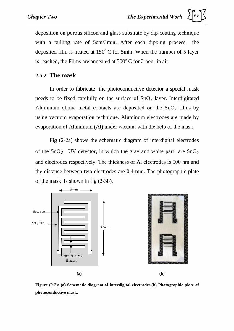
2.5.2 The mask
35
2.6 Fabrication of SnO2/PS photoconductive( UV) detector coated
with a polymer
36
2.6.1 Chemical material:
36
2.6.2 Coating of the SnO2 films/PS by the polymer
36
2.7 Atomic Force Microscopy (AFM)
37
2.8 Structre Measurements 38
2.8.1 X-Ray Diffraction studies 38
2.8.2 Optical Properties
39
2.8.2.1 UV – VIS absorption spectrum
39
2.8.2.2 Photoluminescence Spectrum (PL)
40
2.9 Electrical Properties of the detector
40

2.9.1 Hall Effect Measurement
40
2.9.2 Detector Characteristic Measurement
41
Chapter Three:Results and discaussion 3.1 Introduction
43
3.2 Structure Properties
43
3.2.1 X-ray diffraction results of SnO2 film
43
3.2.2 Atomic Force Microscopy
44
3.3 Optical Properties
47
3.3.1 UV-VIS absorption Spectrum
47
3.3.2 The energy band gap calculation 48
3.3.3 The optical Photoluminescence spectrum
49
3.4 Hall Measurements 50
3.5 The Photodetector Measurements
50
3.5.1 I-V Characteristics
50
3.5.2 The Specific Detectivity ( D*) 53
3.5.3 Photocurrent Gain (G)
53
3.5.4 The Response Time
54

3.6 Conclusion
55
3.7 Suggestions of future work
55
References

List OF Tables
List OF Figures
Table Table Caption Page
(1-1) properties of SnOR2R wurtzite structure 7
(3-1) Hall effect parameters for SnOR2R film deposited on porous silicon
50
Figure Figure Capton Page
(1-1) Types of electron confinement 3
(1-2) Density of states as a function of energy for bulk material, quantum well, quantum wire and quantum dot
4
(1-3) Quantum films(multiple quantum wells superlatices)(1-D quantization)
4
(1-4) structure of SnO2 6

Figure Figure Capton Page
(1-5) Diagram of the reaction mechanism for PS formation
13
(1.6) Relative spectral response for a photo detector and a thermal detector
14
(1-7) photoconductive detector
16
( 1-8) Processes of photoconductive for semiconductor 18
(1-9) The operation circuit diagram of SnOR2R photoconductive detector where; RRdR is the detector element, RRL Ris the load resistance and VRCR is the bias voltage
23
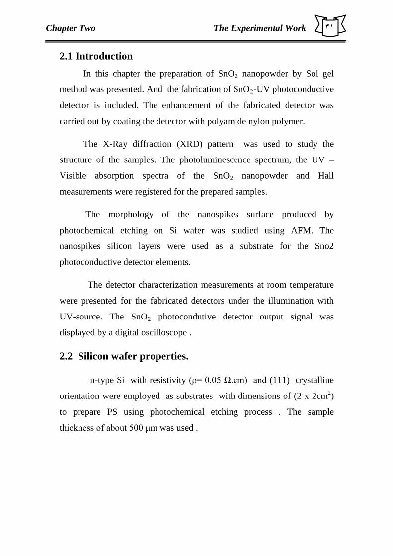
(2-1) The set up of the photochemical etching process ,(photograph of the system)
33
(2-2) (a) Schematic diagram of interdigital electrodes,(b) Photographic plate of photoconductive mask
35
( 2-3) Scanning probe Microscope( Type AA3000) AFM 37
(2- 4) SHIMADZU XRD-6000 X-ray diffractometer (CuKRα Rradiation λ=0.154 nm )
38
( 2-5) Schematic Mask for the Hall effect measurement 40
( 2-6) Schematic diagram of the experimental setup 42
(3-1) XRD pattern of the SnOR2R nanoparticles 44
1T (3-2a) 1T2D×3D Scanning prob microscope image of porous silicon layer of 10 min etching time
45
1T (3-2b) 1TSPM image of SnO2 on PS with etching time 10 min
46
(3-3) 0TThe absorption spectrum of SnOR2 47
Figure Figure Capton Page
(3- 4) Plot of 1T(αhυ)P
2 P1T vs. photon energy (hυ) for SnO R2 48
(3-5) (αhυ)P
2P versus Photon energy for SnO2 thin film 49
( 3-6 ) The variation of the photocurrent of the fabricated SnOR2R UV detector on porous silicon layer as a function of the bias voltage at etching time 10min
51
( 3-7 ) The variation of the photocurrent of the fabricated s
52
(3- 8 ) The photoresponse time of fabricated SnOR2R UV detector1T.The time base on x-axis is 500 μs/div
54

Chapter One
Introduction and Basic Concept
۱
Chapter One Introduction and Basic Concept
1.1 Introduction
Nanotechnology In the last decades, a little word attracted
enormous attention, interest and investigation from all over the world:
“nano”. What it presents in terms of science and technology, which are
also called nanoscience and nanotechnology, is much, much more than
just a word describing a specific length scale. It has dramatically changed
every aspect of the way that we think in science and technology and will
definitely bring more and more surprises into our daily life as well as into
the world in the future.
The classical laws of physics and chemistry do not readily apply at
nano very small scale for two reasons Firstly, the electronic properties of
very small particles can be very different from their larger cousins.
Secondly, the ratio of surface area to volume becomes much higher, and
since the surface atoms are generally most reactive, the properties of a
material change in unexpected ways[1].
Nanoparticles are usually defined as particles less than 100 nm in
diameter[2] . Due to their large surface area to volume ratio, nanoparticles
may have unusual and unique properties not attributed to larger
particles,and are often be more reactive[3,4,5].
Due to the small particle size, the surface area of the nanomaterials is
much larger than that of bulk materials, leading to a large fraction of
surface atoms, large surface energy and reduced imperfections.
Moreover, the nanoparticles can be assembled into various nanostructures
and microstructures. These features give unique electrical, chemical,
optical, and mechanical properties to nanomaterials, which would inspire
the creation and fabrication of new devices and the invention of new
technologies, here is an example of how the interfacial characteristics

۲
Chapter One Introduction and Basic Concept
affect the device applications. Nanomaterials have a significantly lower
melting point than bulk materials, due to a large fraction atoms in the
total amount of atoms [6].
There are two principal ways of manufacturing nanoscale materials; the
top-down nanofabrication starts with a large structure and proceeds to
make it smaller through successive cuttings while the bottom-up
nanofabrication starts with individual atoms and builds them up to a
nanostructure[7].
Several methods have been studied in fabricating these nanostructures,
which include laser ablationP
P, chemical vapor deposition (CVD) and
template-directed growth. In order to integrate one dimensional
nanomaterial into a device, a fabrication method that enables well-
ordered nanomaterials with uniform diameter and length is important.
Template-directed growth is a nanomaterials fabrication method that uses
a template which has nanopores with uniform diameter and length . Using
chemical solutions or electro deposition, nanomaterials are filled into the
nanopores of the templates and, by etching the template, nanowires or
nanotubes with similar diameter and length as the template nanopores are
obtained. Because the size and shape of the nanomaterial depends on the
nanoholes of the template, fabricating a template with uniform pore
diameters is very important. Nanomaterials can be classified by different
approaches such as; according to the X, Y and Z dimensions, according to
their shape and composition. The more classification using is the
order of dimension into 0D (quantum dot), 1D (nanotube, nanowire and
nanorod), 2D (nanofilm), and 3D dimensions such as bulk material
composited by nanoparticles[8].

۳
Chapter One Introduction and Basic Concept
1.2. Types of nano materials P
Nanostructure is divided into three classes as shown in figure (1-1)P
1. One-dimension confinement (quantum well)
2. Two-dimensions confinement (quantum wire)P
3. ThreeP
P-dimensions confinement (quantum dot)[9,10]
Bulk Quantum Well Quantum Wire Quantum Dot
Figure(1-1): Types of electron confinementP
[11]
1.2.1 One – Dimension Confinement (Quantum Well) (Q.W) A quantum well is a potential well that confines particles, which
were originally free to move in three dimensions, in two dimensions,
forcing them to occupy a planar region. Their motions are confined in the
direction perpendicular to the free plane. The effects of quantum
confinement take place when the quantum well thickness becomes
comparable at the de Broglie wavelength of the carriers (generally
electrons and holes), leading to energy levels called "energy subbands",
i.e., the carriers can only have discrete energy values, as in the fig (1-2).
In quantum well the electron are free in Z and Y directions, whereas it is
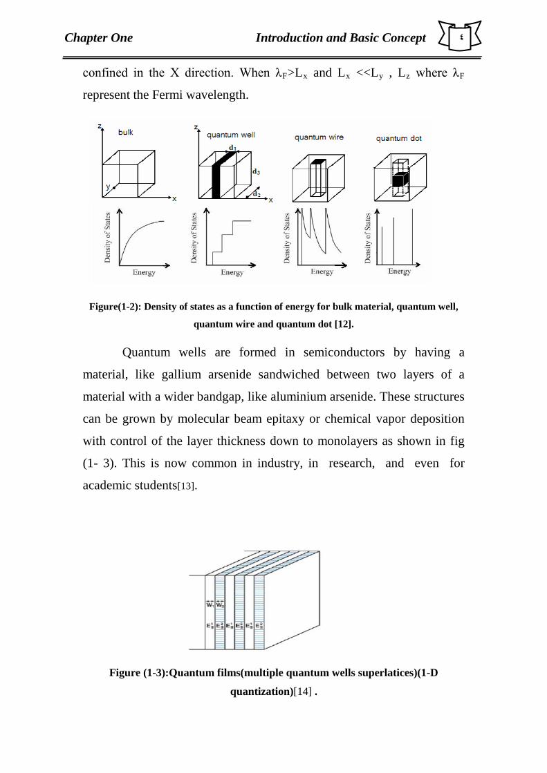
٤
Chapter One Introduction and Basic Concept
confined in the X direction. When λRFR>LRxR and LRxR <<LRyR , LRzR where λRFR
represent the Fermi wavelength.
Figure(1-2): Density of states as a function of energy for bulk material, quantum well,
quantum wire and quantum dot [12].
Quantum wells are formed in semiconductors by having a
material, like gallium arsenide sandwiched between two layers of a
material with a wider bandgap, like aluminium arsenide. These structures
can be grown by molecular beam epitaxy or chemical vapor deposition
with control of the layer thickness down to monolayers as shown in fig
(1- 3). This is now common in industry, in research, and even for
academic students[13].
Figure (1-3):Quantum films(multiple quantum wells superlatices)(1-D
quantization)[14] .
٥
Chapter One Introduction and Basic Concept
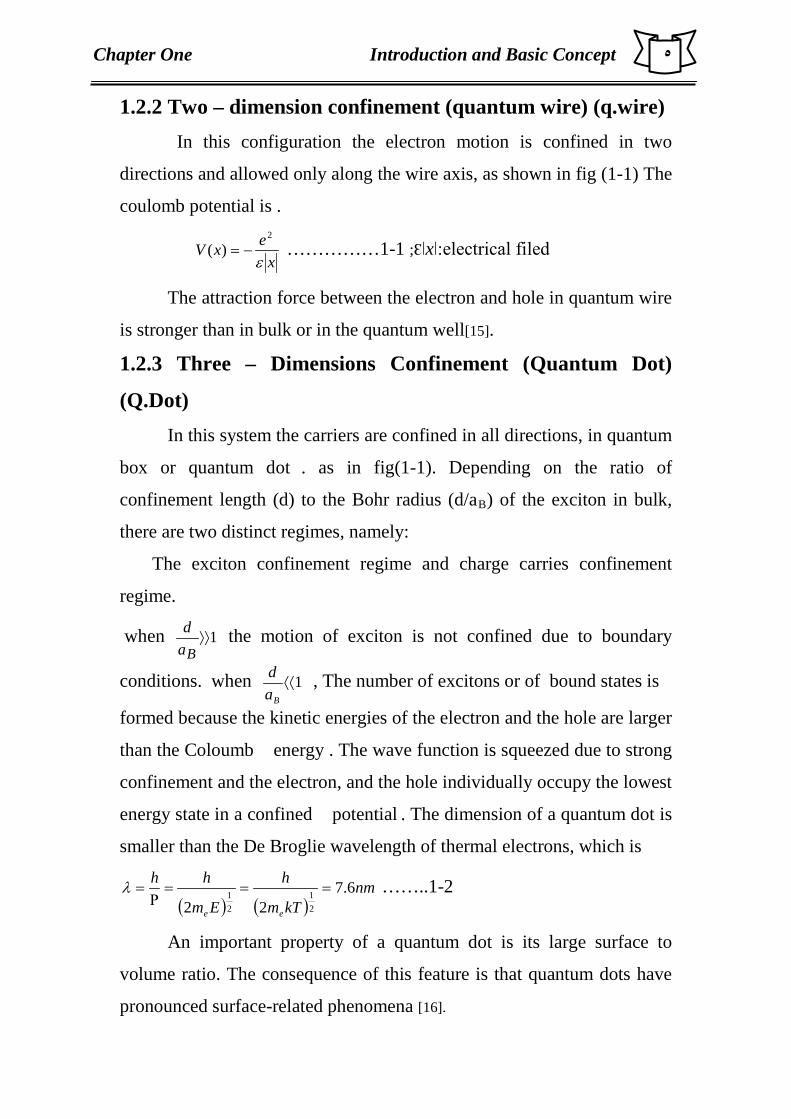
1.2.2 Two – dimension confinement (quantum wire) (q.wire) In this configuration the electron motion is confined in two
directions and allowed only along the wire axis, as shown in fig (1-1) The
coulomb potential is .
x
exVε
2
)( −= ……………1-1 ;Ɛǀxǀ:electrical filed
The attraction force between the electron and hole in quantum wire
is stronger than in bulk or in the quantum well[15]. 1.2.3 Three – Dimensions Confinement (Quantum Dot)
(Q.Dot) In this system the carriers are confined in all directions, in quantum
box or quantum dotP
P. as in fig(1-1). Depending on the ratio of
confinement length (d) to the Bohr radius (d/aRBR) of the exciton in bulk,
there are two distinct regimes, namely:
The exciton confinement regime and charge carries confinement
regime.
when 1⟩⟩Bad the motion of exciton is not confined due to boundary
conditions. when 1⟨⟨Ba
d , The number of excitons or of bound states is
formed because the kinetic energies of the electron and the hole are larger
than the Coloumb energy . The wave function is squeezed due to strong
confinement and the electron, and the hole individually occupy the lowest
energy state in a confined potentialP
P. The dimension of a quantum dot is
smaller than the De Broglie wavelength of thermal electrons, which is
( ) ( )nm
kTm
h
Em
hh
ee
6.722 2
121 ===
Ρ=λ ……..1-2
An important property of a quantum dot is its large surface to
volume ratio. The consequence of this feature is that quantum dots have
pronounced surface-related phenomena [16].P

٦
Chapter One Introduction and Basic Concept
1.3 Tin Oxide SnOR2 R
Tin oxid is an n-type semiconducting metal oxid with awide bandgap
(3.6eV)at 300 K [17,18] . wave – length more then 0.4 µm[19]. is typically
n-type. Because of its high quality of electrical [20],optical (transparent for
visible light and reflective for IR and electrical properties, allied to good
chemical and mechanical stability [21] .
Tin (Sn) is a naturally occurring element that appears in group 14
(4A) of the periodic table. Tin is a silver-white metal that is malleable and
somewhat ductile [22] .
1.4 Structure of SnOR2
Tin oxide has a tetragonal rutile [23] crystalline structure known in
its mineral form as (cassiterite) with point group14 4h D and space group
P42/mnm. The unit cell consists of two metal atoms and four oxygen
atoms. Each metal atom is situated in a midst six oxygen atoms which
approximately.
The lattice parameters of SnO2 are, a =b= 4.7382 Å and c = 3.1871
Å[24,25].
Fig (1-4): structure of SnOR2R [26,27].
۷
Chapter One Introduction and Basic Concept
1.5 properties of SnOR2 Nature of the properties of the SnO2 crystals depend on different
kind of defects and impurities that are present in the structure of this
material. These defects could affect its structural, electronic, optical
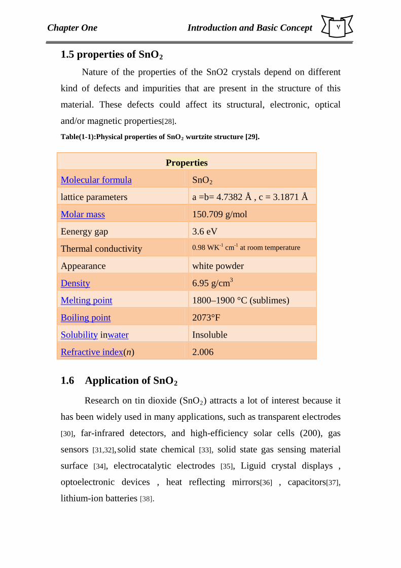
and/or magnetic properties[28]. Table(1-1):Physical properties of SnOR2R wurtzite structure [29].
Properties
1TUMolecular formulaU1T SnOR2
lattice parameters a =b= 4.7382 Å , c = 3.1871 Å
1TUMolar mass U1T 150.709 g/mol
Eenergy gap 3.6 eV
Thermal conductivity 0.98 WKP
-1P cmP
-1P at room temperature
Appearance white powder
1TUDensityU1T 6.95 g/cmP
3
1TUMelting pointU1T 1800–1900 °C (sublimes)
1TUBoiling pointU1T 2073°F
1TUSolubilityU0T1T 0Tin1TUwaterU1T Insoluble
1TURefractive indexU1T(n) 2.006 1.6 Application of SnOR2
Research on tin dioxide (SnOR2R) attracts a lot of interest because it
has been widely used in many applications, such as transparent electrodes
[30], far-infrared detectors, and high-efficiency solar cells (200), gas
sensors [31,32],solid state chemical [33], solid state gas sensing material
surface [34], electrocatalytic electrodes [35], Liguid crystal displays ,
optoelectronic devices , heat reflecting mirrors[36] , capacitors[37],
lithium-ion batteries [38].
۸
Chapter One Introduction and Basic Concept
1.7 Crystalline Silicon
Crystalline Silicon (C- Si ) has a relatively small and indirect band
gap of approximately 1.12 eV . Moreover , highly pure C- Si has a small
exciton binding energy of ~14meV . Silicon is the most prevalent
semiconductor used in microelectronics and photonics; it is produced in
higher volume for lower cost than any other semiconductor. The band gap
of silicon leads to efficient detection of visible light and conversion of
sunlight into electricity. Easily integrated with other microelectronics,
silicon is used in many forms including (crystalline, amorphous, and
porous) in numerous optoelectronic devices. Optical quality silicon is
highly transparent in the far – infrared region and opaque in the visible
and ultraviolet region P
P. Silicon surface has high absorbtivity for oxygen
and the growth rate of oxide layer on silicon surface is nearly (2nm/min)
under ambient condition. This oxide layer has a considerable effect on the
absorbity of the surface for photons of energies higher than 6eV.
Reducing dimensionality of bulk silicon to nano-scale silicon
(Porous silicon) leads to appreciable change in optical , electrical and
electronic properties[39].
1.8 Silicon structure Silicon is the most common metalloid , one of only a very few
elements that have characteristics of both metals and non-metals. It is a
semiconductor material, which has the symbol Si and atomic number 14.
Silicon is the eighth most common element in the nature by mass, but
very rarely occurs as the pure free element in nature. It is more widely
distributed in dusts, sands, planetoids and planets as various forms of
silicon dioxide (silica) or silicates. Silicon, like carbon and germanium,
crystallizes in a diamond cubic crystal structure. The lattice spacing for

۹
Chapter One Introduction and Basic Concept
silicon is 0.5430710 nm. Silicon lattice has a diamond-like structure and
it consists of two interpenetrating FCC lattice, silicon is also part of the
the carbon family.
When considering silicon as a material for optoelectronic applications,
device for which conventional silicon technology falls short is the
light emitter, since crystalline silicon is an inefficient light - emitting
material. Because silicon is an indirect band gap material (1.12 eV) which
leads to low optical efficiency.
1.9 Silicon properties
Silicon is a metalloid, an element with properties of both metals and
non-metals. The melting point of silicon is 1410°C and the boiling point
is 2355°C. Its density is 2.33 g/cmP
3P. Silicon is a semiconductor, A
semiconductor is a substance that conducts an electric current better than
a non-conductor—like glass or rubber—but not as a conductor—like
copper or aluminum Silicon is a relatively inactive element at room
temperature. It does not combine with oxygen or most other elements.
Water, steam, and most acids have very little affect on the element. At
higher temperatures, however, silicon becomes much more reactive. In
the molten (melted) state, for example, it combines with oxygen,
nitrogen, sulfur, phosphorus, and other Porous Silicon material is a
network consisting of pores elements separated by thin columns and
contains nano-meter sized silicon crystallites, as a result, PS is
characterized by a very large internal surface. Porous silicon formed
under different anodization conditions exhibits a variety of rich and
complex structure with many features [40].

۱۰
Chapter One Introduction and Basic Concept
Porous silicon (PS) 1.10
The technology of porous silicon seems to have advantages since
the specific dimensions of PS stem can be reduced down to nanometre
size. It is reasonable to expect significant increase of detector’s
sensitivity if PS technology were introduced in its production. Additional
advantages are expected due to the quantum confinement effect, which is
obtained conventionally by anodization of silicon substrates. Crystallites
of silicon formed by this means can present diameters varying from units
of nanometers to tens of micrometers, depending on formation parameters
(current density, electrolyte concentration, etching time, and substrate
type). This characteristic, that is, the possibility of porosity control,
makes PS suitable for several applications on gas sensing.
Porous silicon technologies have many applications in
semiconductor technology, optoelectronics, chemical, biological sensors
and other fields of science. Electrochemical etching of a silicon wafer
surface, under different conditions and additional processing, changes the
optical and electrical properties of porous silicon layers widely.
The physical properties of porous silicon are fundamentally determined
by the porosity of pores [41,42,13].
1.11 Preparation Techniques
1.11.1 The Etching Process
Various etching techniques can be divided into wet and dry
categories according to the chemical reaction on the gas-solid and liquid-
solid interface. In the wet etching, chemical acid solutions are used to
dissolve silicon substrate by chemical reactions [43]. Wet etching of
silicon can be achieved in different ways [44,45]:

۱۱
Chapter One Introduction and Basic Concept
• Laser Induced Etching process (LIE)
• Photochemical Etching process (PCE)
• Photo electro Chemical Etching process (PECE)
• Stain Etching process
• Electrochemical Etching process
in our work Photochemical Etching process used
1.11.2 Photochemical Etching Mechanism
A silicon wafer is known to be inert in Hydro Furan Acid acid but a
chemical reaction can be initiated when holes reach the surface.
Therefore, in an n-type silicon valence-band holes are required at the
sample surface for porous silicon formation [46]. Photochemical technique
has been used to produce PS, which does not involve an externally
applied bias. In this technique, the light (laser) is used to supply the
required holes in the irradiation area of Si wafer to initiate the process[47]
.Generally, when a semiconductor is immersed in an aqueous solution
that contains electron acceptor species, charge transfer occurs at the
semiconductor-electrolyte interface. This charge transfer creates a space-
charge layer in the semiconductor resulting in a band bending upward in
an n-type And downward p-type material [48]. An n-type Si wafer is
immersed in aqueous HF acid and illuminated with laser light, a large
number of electron-hole pairs are generated in (C-Si) in the irradiated
area. a percentage of both charges will diffuse rather than immediately
recombine due to the indirect band gap in silicon. Furthermore, because
of the internal field caused by band bending, holes are driven into the
surface to initiate the etching process. These holes help to substitute
fluoride by hydrogen on the passivity Si surface and a Si-F bond is
established Due to the polarizing influence included by the Si-F, the
electron density of the Si-Si bond is lowered, which is further attacked by
۱۲
Chapter One Introduction and Basic Concept
HF finally, the detachment of a Si atom occurs in the form of SiFR4 Ror
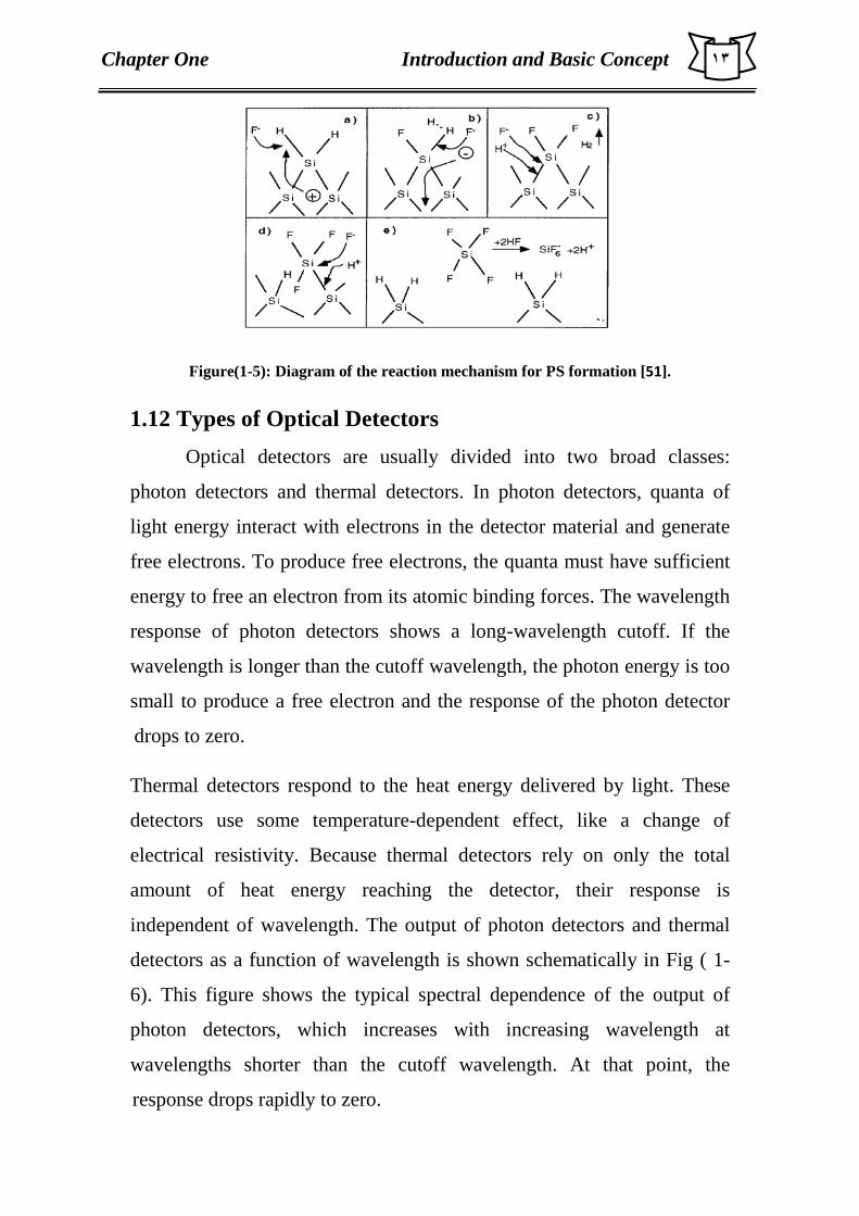
SiFR6R as etch products.See fig (1-5).
The chemical reaction of this process can be expressed as follows.
↑++−→+++ 2421242 HSiFHnSihFHnSi ………..(1-3)
On the other hand, electronically current flows from the back side of
the wafer through the electrolyte completing the electrical circuit and this
current enhances the etching process in the wafer thickness direction.
The electrical field effects can lead to preferential transport of
holes to the bottom of pores rather than to pore walls. This leads to
preferential etching at the bottom of the pores and since there is no
applied potential, the only source of an electrical field inside the Si would
be from band bending while there is certainly a band offset between bulk
Si and a PS layer at the interface, this band offset, which results from
quantum confinement, is sufficient to lead to a focusing effect.
It is expected that the microstructures and properties of the produced PS
material would depend upon the processing parameters, such as the
photon energy, power density and irradiation time. It is of great interest
both to develop a control of the fabrication process and to monitor the
size of the nanostructure in the PS samples. Therefore, for more detailed
investigation and characterization of the constituent nanostructure,
Raman and PL spectroscopies are often employed. These can give us
significant information on the size distribution of the nanocrystallites
present in laser etched PS [49,50].
۱۳
Chapter One Introduction and Basic Concept
Figure(1-5): Diagram of the reaction mechanism for PS formation [51].
1.12 Types of Optical Detectors Optical detectors are usually divided into two broad classes:
photon detectors and thermal detectors. In photon detectors, quanta of
light energy interact with electrons in the detector material and generate
free electrons. To produce free electrons, the quanta must have sufficient
energy to free an electron from its atomic binding forces. The wavelength
response of photon detectors shows a long-wavelength cutoff. If the
wavelength is longer than the cutoff wavelength, the photon energy is too
small to produce a free electron and the response of the photon detector
drops to zero.
Thermal detectors respond to the heat energy delivered by light. These
detectors use some temperature-dependent effect, like a change of
electrical resistivity. Because thermal detectors rely on only the total
amount of heat energy reaching the detector, their response is
independent of wavelength. The output of photon detectors and thermal
detectors as a function of wavelength is shown schematically in Fig ( 1-
6). This figure shows the typical spectral dependence of the output of
photon detectors, which increases with increasing wavelength at
wavelengths shorter than the cutoff wavelength. At that point, the
response drops rapidly to zero.

۱٤
Chapter One Introduction and Basic Concept
The figure also shows how the output of thermal detectors is
independent of wavelength, and extends to longer wavelengths than the
response of photon detectors[52].
1.12.1 Thermal detectors
Thermal detectors are sensing the changing in temperature
produced by absorption of incident radiation. In thermal detectors, the
radiation is absorbed by the lattice of material, causing heating of the
lattice. The change in the temperature of the lattice by the absorption
causes a change in the electrical properties. These detectors are generally
operated at room temperature. Fig (1-6) shows the mechanism
responsible for the absorption of the radiation which is itself wavelength
independent [53].
Figure(1-6): Relative spectral response for a photo detector and a thermal
detector [55].
1.12.2 Photon detectors
Photon detectors respond in proportional to incident photon rates
rather than to photon energies (heat). Thus , the spectral response of an

۱٥
Chapter One Introduction and Basic Concept
ideal photon detector is flat on an incident-photon-rate basis but linearly
rising with wavelength on an incident-power (per watt) basis .In photon
detectors the incident photons are absorbed within the material by
interaction with electrons. The observed electrical signal results from
changing the electronic energy distribution. The photon detectors
measure the rate of arrival of quanta and show a selective wavelength
dependence of the response per unit incident radiation power as shown in
Fig (1-6) [54].
Photon detectors have a small sizes minimum noise, low biasing
voltage, high sensitivity, high reliability, and fast response time.
Basically, if a photon of sufficient energy excites an electron from
a nonconducting state into a conducting state, the photoexcited electron
will generate current or voltage in the detector. The electronic excitation
requires that the incident photon energy must be equal to or greater than
the electronic excitation energy. In other words, the excitation condition
is: νhexc ≤Ε .........1-4
or
cexc λ
242.1≤Ε
...........1-5
where ERexcR is the electronic excitation energy in electron volts.
λRcR is the free space wave length in micrometers.
h=P
P4.136×10 P
-15Pev.s ,C=3×10 P
8Pm∕s
Most of photon detectors have a detectivity that is one or two
orders of magnitude greater than thermal detector, and the response time

۱٦
Chapter One Introduction and Basic Concept
of photon detectors is very short due to direct interaction between the
incident photons and the electrons of the detector material this interaction
is called photo effect.
Photon detectors include photoconductive (PC), photovoltaic (PV)
Photoemissive detectors. While the study now is specializing in
photoconductive detectors; therefore, we will concentrate on it in next
part [56].
1.13 Photoconductive Detectors
Since the nineteenth century it has been known that certain
materials have the power of changing their resistance on exposure to
light. Such materials are known as photoconductors, which is one of the
first type of semiconductor photon detector. The photoconductive
detector consists of a single crystal of semiconductor material with two
ohmic contacts, and a voltage applied between them. The semiconductor
is conducting, and therefore some current flowing even without light
shining on material (dark current). See fig (1- 7).
Fig (1-7): photoconductive detector [57].
۱۷
Chapter One Introduction and Basic Concept
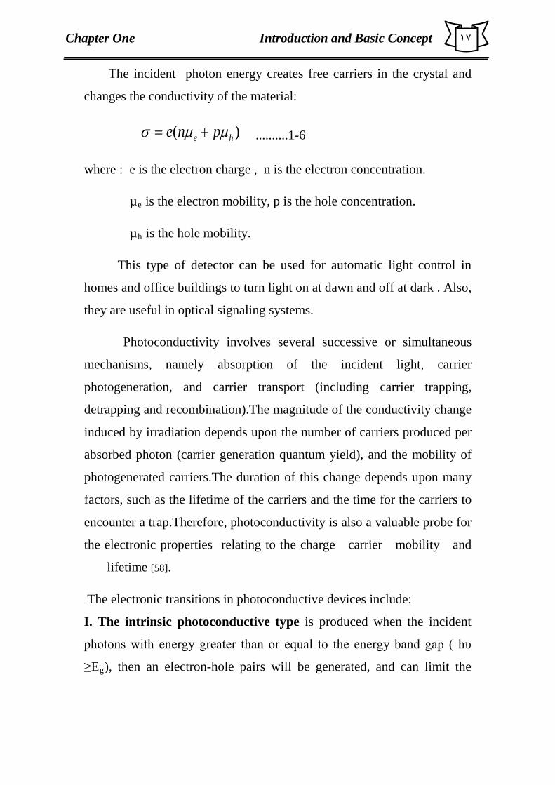
The incident photon energy creates free carriers in the crystal and
changes the conductivity of the material:
)( he pne µµσ += ..........1-6
where : e is the electron charge , n is the electron concentration.
µReR is the electron mobility, p is the hole concentration.
µRhR is the hole mobility.
This type of detector can be used for automatic light control in
homes and office buildings to turn light on at dawn and off at dark . Also,
they are useful in optical signaling systems.
Photoconductivity involves several successive or simultaneous
mechanisms, namely absorption of the incident light, carrier
photogeneration, and carrier transport (including carrier trapping,
detrapping and recombination).The magnitude of the conductivity change
induced by irradiation depends upon the number of carriers produced per
absorbed photon (carrier generation quantum yield), and the mobility of
photogenerated carriers.The duration of this change depends upon many
factors, such as the lifetime of the carriers and the time for the carriers to
encounter a trap.Therefore, photoconductivity is also a valuable probe for
the electronic properties relating to the charge carrier mobility and
lifetime [58].
The electronic transitions in photoconductive devices include:
I. The intrinsic photoconductive type is produced when the incident
photons with energy greater than or equal to the energy band gap ( hυ
≥ERgR), then an electron-hole pairs will be generated, and can limit the

۱۸
Chapter One Introduction and Basic Concept
maximum wavelength cutoff wavelength (λRcR) that detectors work is given
by eq(1-5) P
P.
II.The extrinsic photoconductive type : Since semiconductors have
states located ( energy levels ) either as donors or acceptors in the band
gap ; The energy required to ionize these must be smaller than the
intrinsic energy , so that the quantum energy with hυ > ERi R, where ERi
Ractivation energyR Rfor donors ( ERD R) or acceptor ( ERAR ) , is absorbed then
transition of electron from donor level to the conduction band for n-type
or, transition of holes from the valence band to acceptor levels for p-type
takes place but not both. In both cases the concentration of carrier
increases so that the conductivity of semiconductor will increase also .
This type is called photoconductive detectors as shown in figure (1-8)
.The cut off wave length ( λRcR ) is given by eq(1-5) P
P .
Figure( 1-8): Processes of photoconductive for semiconductor
(a) Intrinsic (b) Extrinsic P
[59]P.
Other types of photoconductivity are possible which are not
associated with a change in the free-carrier concentration. For example,
when long-wavelength electromagnetic radiation, which does not cause
interband migration and does not ionize impurity center, is absorbed by
free carriers, the energy of the carriers is increased. Such an increase
۱۹
Chapter One Introduction and Basic Concept
leads to a change in carrier mobility and, consequently, to an increase in
electrical conductivity. Such secondary photoconductivity decreases at
high frequencies and is not frequency dependent at low frequencies. The
change in mobility upon exposure to radiation may be caused not only by
increasing in carrier energy but also by the effect of the radiation on
electron scattering in the crystal lattice [60].
1.14 The Figure of Merit
There are many parameters affecting the performance of the
detectors. These parameters are:
1.14.1 Responsivity ( RRλ R)
Responsivity is defined as the ratio between the output electrical
signals (voltage or current) to the incident radiation power or is defined as
the r.m.s signal voltage to the r.m.s value of the incident radiation power.
The responsivity for monochromatic light of wavelength incident
normally is given by[61] .
in
ph
PI
R =λ (Amp∕Watt) or inP
VR =λ (Volt∕ Watt) ……..1-7
where :
IRphR = photocurrent flowing between the electrodes.
V= signal voltage
1.14.2 Photocurrent Gain (G)
The photocurrent gain G of a detector is defined as the number of
charge carriers flowing between the two contact electrodes of a detector
per second for each photon absorbed per second that is .

۲۰
Chapter One Introduction and Basic Concept
rT
G τ= …………………… 1-8
where τ is the carrier lifetime , TRrR is the transit time , which is expressed
by :
B
r VT
⋅=µ
2 ……………………..1-9
where ℓ is the distance between electrodes , μ is the majority
carrier mobility , and VRBR is the bias voltage applied to the sample[60].
1.14.3 The Noise in Detectors (IRnR)
The noise is refered to the signal generated in the detector at the
absence of the radiation . The relation between dark current and noise
current is [57] :
IRn R= ( 2e IRdR Δf )P
1/2P …………….……..1-10
Where IRd R is dark current , Δf is bandwidth.
1.14.4 Noise Equivalent Power ( NEP)
NEP is defined as the root mean square ( r.m.s ) incident radiant
power falling on the detector that is required to produce an ( r.m.s ) signal
voltage or current equal to the ( r.m.s ) noise voltage or current at the
detector output . It is expressed as [62]:
NEP = IRn R/ RRλR …………………………….. 1-11
The detection capablility of the detector improves as the NEP
decreases .
۲۱
Chapter One Introduction and Basic Concept
1.14.5 Detectivity ( D ) and Specific Detectivity ( D* ) :
The detectivity ( D ) is defined as the signal – to – noise ratio per
unit incident radiation power and it is defined as:
D = 1/NEP = RRλR / IRn R (WattP
-1P) …………1-12
Specific detectivity D* (normalized detectivity ) : it is the
detector signal – to – noise ratio when 1 Watt of optical power is incident
on the detector with optical area 1 cmP
2 Pand the noise is measured with a
band width of 1 Hz . It is used because it is normally dependent on the
size of the detector and the bandwidth of the measurement circuit, while
D depends on both . The peak value of D* at specific wavelength can be
written asP
P[63] ;
D* = D ( A Δ f )P
1/2 P …………….……….1-13
Or D* = RRλR ( A Δ f )P
1/2P / IRn R………….…..…… 1-14
The value depends on the wavelength of the signal radiation and
the frequency at which it modulated P
.
1.15 The mathematical model of the photoconductive
detector
The photocurrent generated in the detector circuit shown in figure
(2-5a) when the detector elements are illuminated by the UV radiation
can be written as[39,57];
GNei ...η= ……….1-15
where η is the quantum efficiency.
e is the electronic charge.
۲۲
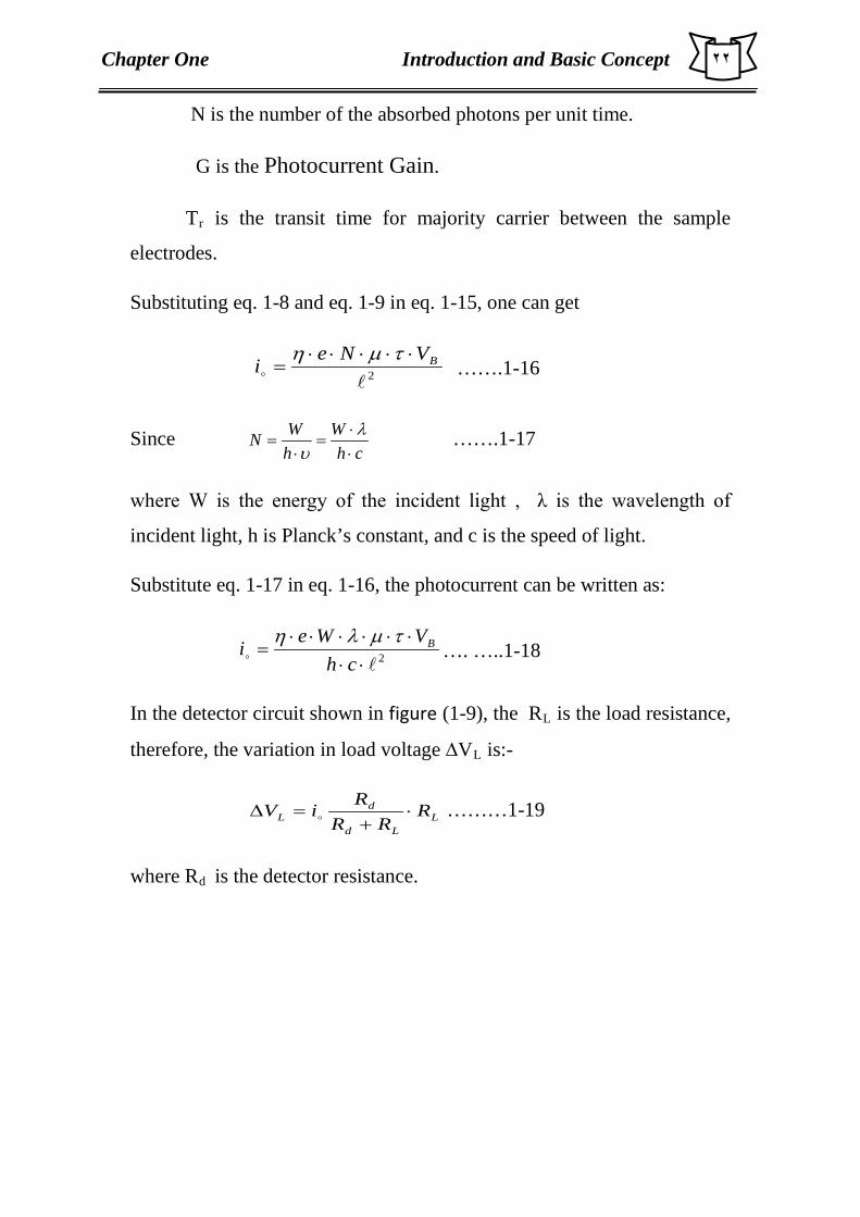
Chapter One Introduction and Basic Concept
N is the number of the absorbed photons per unit time.
G is the Photocurrent Gain.
TRrR is the transit time for majority carrier between the sample
electrodes.
Substituting eq. 1-8 and eq. 1-9 in eq. 1-15, one can get
2
BVNei ⋅⋅⋅⋅⋅=
τµη …….1-16
Since ch
WhWN
⋅⋅
=⋅
=λ
υ …….1-17
where W is the energy of the incident light , λ is the wavelength of
incident light, h is Planck’s constant, and c is the speed of light.
Substitute eq. 1-17 in eq. 1-16, the photocurrent can be written as:
2 ⋅⋅
⋅⋅⋅⋅⋅⋅=
chVWei Bτµλη
…. …..1-18
In the detector circuit shown in figure (1-9), the RRLR is the load resistance,
therefore, the variation in load voltage ∆VRLR is:-
LLd
dL R
RRR
iV ⋅+
=∆ ………1-19
where RRd R is the detector resistance.

۲۳
Chapter One Introduction and Basic Concept
Figure (1-9): The operation circuit diagram of SnOR2R photoconductive detector
where; RRdR is the detector element, RRL Ris the load resistance and VRCR is the bias
voltage.
for RRdR >> RRLR
dL RiV ⋅≈∆∴ …….1-20
for dwRd ⋅⋅
=σ
……….1-21
where σ is the conductivity , w is the width of the detector and d is the
height of the detector.
Substitute eq. 1-18 and eq. 1-21 in eq. 1-20, the variation voltage across
the load resistance can be given as:
dwch
VWeV BL ⋅⋅
∗⋅⋅
⋅⋅⋅⋅⋅⋅=∆∴
σλτµη
2 …….1-22
Rd
VC
RL
0.1 μF Output
Detector
۲٤
Chapter One Introduction and Basic Concept
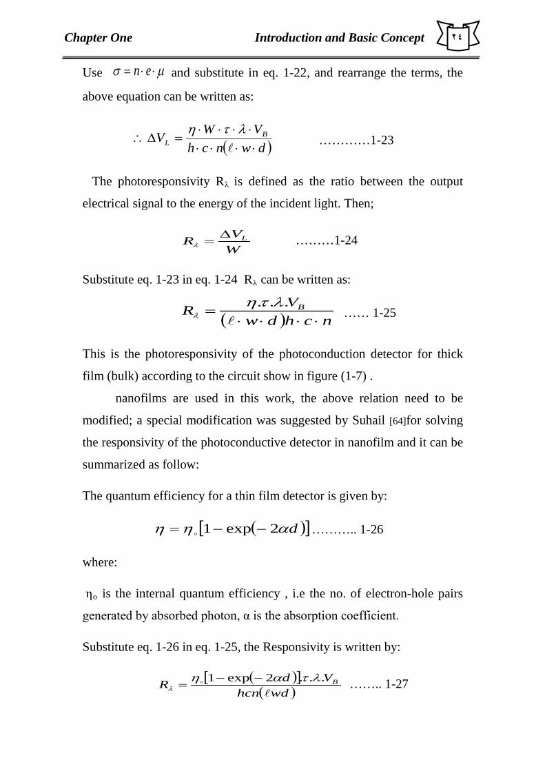
Use µσ ⋅⋅= en and substitute in eq. 1-22, and rearrange the terms, the
above equation can be written as:
( )dwnchVWV B
L ⋅⋅⋅⋅⋅⋅⋅⋅
=∆∴
λτη …………1-23
The photoresponsivity RRλ Ris defined as the ratio between the output
electrical signal to the energy of the incident light. Then;
WVR L∆
=λ ………1-24
Substitute eq. 1-23 in eq. 1-24 RRλR can be written as:
( ) nchdwVR B
⋅⋅⋅⋅=
... λτηλ …… 1-25
This is the photoresponsivity of the photoconduction detector for thick
film (bulk) according to the circuit show in figure (1-7) .
nanofilms are used in this work, the above relation need to be
modified; a special modification was suggested by Suhail [64]for solving
the responsivity of the photoconductive detector in nanofilm and it can be
summarized as follow:
The quantum efficiency for a thin film detector is given by:
( )[ ]dαηη 2exp1 −−= ……….. 1-26
where:
ηRoR is the internal quantum efficiency , i.e the no. of electron-hole pairs
generated by absorbed photon, α is the absorption coefficient.
Substitute eq. 1-26 in eq. 1-25, the Responsivity is written by:
( )[ ]( )wdhcn
VdR B
...2exp1 λταη
λ−−
= …….. 1-27

۲٥
Chapter One Introduction and Basic Concept
For a thin film detector, the absorption coefficient is low and the
condition 2αd << 1 is always fulfilled in the thin film detectors; the
efficiency can be written as:
( )dαηη 2= where ηRoR in this case equal to 1, then the relation 1-27 can
be written as:
( )wdhcndVR B
)2.(.. αλτλ = ……… 1-28
Relation 1-28 can be written as:
)(2...whcn
VR B
αλτλ = ………… 1-29
The bias voltage (applied voltage) VRBR is limited to the allowed
power that can be passed through the thin film detector. This is called the
bias power which is;
dRiu .2= …………… 1-30
where i is the circuit current, which is given by:
( )Ld
B
RRVi+
= …………. 1-31
Substitute eq. 1-31 in eq. 1-30, the bias power u is written as:
( ) d
Ld
B RRR
Vu .2
2
+= ……….. 1-32
For RRdR >> RRLR the bias power became:
d
B
RVu
2
= ……………… 1-33

۲٦
Chapter One Introduction and Basic Concept
The bias power density ( )wRVu
d
B
⋅=′
2
…….. 1-34
Thus, ( )wRuV dB ⋅′= .. …… 1-35
Substitute eq. 1-35in eq. 1-29, and rearrange the terms, the following
formula can be considered:
′
=
nwuR
hcR d ταλλ
..2 2/1
……. 1-36
When the first term is constant, the second term is square root, and the
third term is linear. These results show that the photoresponsivity (RRλR) is
depending too much on the third term
nτα. .
1.16 Literature Survey Yang Liu1et.al (2000)[60] had synthesized two SnOR2R
nanoparticles by hydrothermal method at 170ºC and 180ºC, respectively.
Transmission electron microscope observations reveal that the diameters
of both the nanoparticles were around 6 nm. At the same time, surface
photovoltage spectroscopy measurements, showed that the nanoparticle
synthesized at 180ºC, had more surface electronic states at 0.3 eV below
the conduction band than the one synthesized at 170ºC. This means that
the temperature chosen in hydrothermal synthesis had significant
influence on the surface electronic characteristics of resultant SnOR2R
nanoparticles but the effect on their sizes was not obvious.
Feng Gu a et.al (2003)[65] had prepared SnOR2 Rnanoparticles by a
simple sol–gel method. XRD measurement indicates that the diameter of
the prepared particle was about 2.6 nm. FTIR and the UV–Vis absorptive
spectra of the samples had also been investigated. And the PL exhibits

۲۷
Chapter One Introduction and Basic Concept
two bands at 400 and 430 nm, respectively. The luminescence was related
to the recombination of electrons in singly occupied oxygen vacancies
with photo excited holes in the valence bond.
SANJAY R DHAGE et.al (2004)[66] had reported that simple gel
to crystal conversion had been followed for the preparation of
nanocrystalline SnOR2R at 80–100°C under refluxing conditions. Freshly
prepared stannic hydroxide gel was allowed to crystallize under refluxing
and stirring conditions for 4–6 h. Formation of nano crystallites of SnOR2R
was confirmed by x-ray diffraction (XRD) studied. Transmission electron
microscopic (TEM) investigations revealed that the average particale size
was 30 nm for these powders.
J.J. Valenzuela-Ja et.at (2004)[67] had deposited metal films of Sn, In
and In–Sn on glass substrates at room temperature by means of the DC
sputtering technique.. A film of the corresponding metal oxides was
obtained after thermal annealing the metal for 1 h in air at temperature
from 350 to 500P
oP C. The oxide film was studied besides that, transmission
and reflection spectroscopy, by measurements of their sheet resistance
between coplanar electrodes. The results showed that materials with the
properties of transparent conductive oxides (TCO) films could be
obtained by this process.
Luhua Jiang et.al (2005)[68] had synthesized tin oxide
nanoparticles by heating ethylene glycol solutions containing SnClR2R at
atmospheric pressure. TEM micrographs showed that the obtained
material were spherical nanoparticles, the size and size distribution
depends on the initial experimental conditions of pH value, reaction time,
water concentration, and tin precursor concentration. The XRD pattern
۲۸
Chapter One Introduction and Basic Concept
result showed that the obtained powder was SnOR2R with tetragonal
crystalline structure. On the basis of UV/VIS and FTIR characterization,
the formation mechanism of SnOR2R nanoparticles was deduced.
Chunjoong Kim et.al( 2005) [69] SnOR2R nanoparticles with
different sizes of 3, 4, and 8 nm had been synthesized using a
hydrothermal method at 110, 150, and 200 C, respectively. The results
showed that the 3 nm-sized SnOR2R nanoparticles had a superior capacity
and cycling stability as compared to the 4 and 8 nm-sized ones. The 3
nm-sized nanoparticles exhibited an initial capacity of 740 mAh/g with
negligible capacity fading. Transmission electron microscope(TEM) and
X-ray diffraction (XRD) confirmed that the 3 nm-sized SnOR2
Rnanoparticles after electrochemical tests did not aggregate into larger Sn
clusters, in contrast to those observed with the 4 and 8 nm-sized ones.
K. ANANDAN et.al (2008)[32] had synthesized tetragonal phase
SnOR2R nanocrystals via facile solvothermal process by using SnClR4R.5HR2RO
and HCl at different temperature. The phase, size and purity of the
resultant products were characterized by means of powder X-ray
diffraction (XRD).
M. M. Bagheri-Mohagheghia et.al (2008)[70] Nano-crystalline
SnOR2 Rparticles had been synthesized by sol–gel process using a simple
starting hydro-alcoholic solution consisting of SnClR4R, 5HR2RO and citric
acid as complexing and ethylene glycol as polymerization agents. The
XRD patterns showed SnOR2R-cassiterite phase in the nano-powders, and
size of crystals increases by increasing the annealing temperatures. The
optical direct band gap values of SnOR2R nano-particles were calculated to
be about 4.05–4.11 eV in the temperature range 300–700º C by optical
absorption measurements. These values exhibited nearly a 0.5 eV blue
shift from that of bulk SnOR2R (3.6 eV), which was related to size decrease
۲۹
Chapter One Introduction and Basic Concept
of the particles and reaching to the quantum confinement limit of nano-
particles.
S. MAJUMDER(2009)[71] had fabricated SnOR2R thin films by a
wet chemical process, using SnClR2R·2HR2RO as a tin containing precursor.
The films obtained were subjected to optical, X-ray diffraction (XRD),
microstructural, FTIR and Raman studies.
Rohana Adnan et.al (2010)[ 72] had prepared SnOR2R nanoparticles
using a simple sol-gel technique with varying reaction parameters such
as concentration of ammonia, ammonia feed rate and reaction
temperature. The Size obtained was in the range of 4 to 5.6 nm and the
surface area was found to be between 76 to 114 mP
2P.
Lucky M Sikhwivhilu et.al (2010)[73] had synthesized tin oxide
(SnOR2R) nanoparticles by using wet chemical process (i.e. chemical
precipitation and sol-gel processes). The results showed that variation of
citric acid concentration directly influences the particle size and the BET
specific surface area with size range of 19 to 100 nm.
L. C. Nehru et.al(2012) [74] Nanocrystalline tin oxide (SnOR2R)
powders were been synthesized by a low temperature chemical
precipitation method. Crystallographic parameters such as crystallite size,
lattice parameters and dislocation density in SnOR2R nanocrystalline
powders were calculated by Rietveld analysis. The average crystallite size
of 9 - 43 nm was obtained for SnOR2R powders through controlled heat
treatment process. The washed powders morphology was almost
spherical in shape and average agglomerate crystal size was between 0.2
– 0.4 μm.
Ganesh E Patiletet.al (2012) [75] Preparation and characterization
of SnOR2R nanoparticles by hydrothermal route had been demonstrated
SnOR2 Rnanoparticles using a simple hydrothermal route in the presence of

۳۰
Chapter One Introduction and Basic Concept
the surfactant hydrazine at 100 °C for 12 h. The XRD pattern of the as-
prepared sample was indexed to the tetragonal structure of SnOR2R, and the
calculated particle size was 22.4 nm, which was further confirmed by
TEM. Spectrum showed the band gap of the synthesized SnOR2R was 3.6
eV.
1.17 Aim of the Present work
In this work the SnOR2R nanopowder was deposited on porous silicon
by dip coating technique to form UV photoconductive detector in order to
improve the response time of the detector. The improvement based in two
mechanisms the first is improve the structure of coating film on the
silicon layer through developing the porous layer on n-type silicon
substrate and the second is the functionalization of the detector surface by
coating the sensitive area by poly amide nylon polymer.

Chapter Two
Experimental Work
۳۱
Chapter Two The Experimental Work
2.1 Introduction In this chapter the preparation of SnOR2R nanopowder by Sol gel
method was presented. And the fabrication of SnOR2R-UV photoconductive
detector is included. The enhancement of the fabricated detector was
carried out by coating the detector with polyamide nylon polymer.
The X-Ray diffraction (XRD) pattern was used to study the
structure of the samples. The photoluminescence spectrum, the UV –
Visible absorption spectra of the SnOR2R nanopowder and Hall
measurements were registered for the prepared samples.
The morphology of the nanospikes surface produced by
photochemical etching on Si wafer was studied using AFM. The
nanospikes silicon layers were used as a substrate for the Sno2
photoconductive detector elements.
The detector characterization measurements at room temperature
were presented for the fabricated detectors under the illumination with
UV-source. The SnOR2R photocondutive detector output signal was
displayed by a digital oscilloscope .
2.2 Silicon wafer properties.
n-type Si with resistivity (ρ= 0.05 Ω.cm) and (111) crystalline
orientation were employed as substrates with dimensions of (2 x 2cmP
2P)
to prepare PS using photochemical etching process . The sample
thickness of about 500 μm was used .
۳۲
Chapter Two The Experimental Work
2.3 Sample Preparation
The manufacturing of PS relies on the wet etching of wafers .
silicon substrates of (2x2cmP
2P) dimensions are cleaned to remove any
contamination on the surface, and the following cleaning procedures were
carried out :
1 -The silicon wafers were washed in diluted HF ( 1:10 ) concentration
for 15 min.
2- The wafer then immersed in distilled water for several times, and later
they were rinsed in methanol for 10 minutes and also in distilled water.
3- Finally, the samples were dried in oven, at 50P
ºPC.
2.3.1 Preparation of porous silicon layer by photochemical
etching
The photochemical etching is electrodeless process since there is
no applied bias voltage during the etching, This process is carried out by
using ordinary light source.
The setup shown in fig (2-1) has been used for the photochemical
etching process. The setup consists of a Quartz Tungsten Halogen lamps
(250W) integrated with dichroic ellipsoidal mirror supplied from Philips
Company , focusing lens and the diluted etching acid in Teflon container .
۳۳
Chapter Two The Experimental Work
Figure (2-1): The set up of the photochemical etching process,(photograph of the
system).
The n-type Si wafer of ( 0.05 Ω.cm ) resistivity was used as a
starting substrate in the photochemical etching. The samples of ( 2 x 2
cmP
2P ) dimensions were cut from the wafer and rinsed with acetone and
methanol to remove dirt. In order to remove the native oxide layer on the
samples, they were etched in diluted (10 %) HF acid. After cleaning the
samples they were immersed in HF acid of 50 % concentration and
ethanol (1:1)) in a Teflon beaker. The samples were mounted in the
beaker on two Teflon tablets in such a way that the current required for
the etching process could complete the circuit between the irradiated
surface and the bottom surface of the Si sample.
Conecting wire
Power Supply
lens
Teflon container
Light Source
۳٤
Chapter Two The Experimental Work
The light source was vertically mounted by a holder above the
sample, aligned and focused by Quartz lens of (3.87cm) focal length to
form a circular spot with a suitable power density. The lens was mounted
on a driven holder for precise focusing adjustment. The distance from the
lamp to the lens was about 30 cm and from the lens to the sample 14 cm.
The PS was formed on the illuminated side of the sample. The
photoetching irradiation times was chose to be about 10 minutes
At the end of the photochemical etching process, the sample were rinsed
with ethanol and stored in a glass containers filled with methanol to avoid
the formation of oxide layer above the nanospikes film. The nanospikes
silicon layers were used as a substrate for the SnOR2R photoconductive
detector elements.
2.4 Preparation of SnOR2R nanopowder by Sol gel method
SnOR2R nanopowders were prepared by means of dissolving 2 g
(0.1 M) of tin tetrachloride (SnClR5R.5HR2R O) in 100 ml distilled water.
After complete dissolution, ammonia solution was added to the above
solution by drop wise under stirring until pH was 1. The dropping rate
must be well controlled for chemical homogencity. White gel precipitate
is formed and its allowed to settle for 12 h. then the result gel were
washed and filtered with distilled water and then dried at 80P
oPC for 24
hours in order to remove water molecules. Finally Tin Oxide
nanopowder is formed at 500P
oPC.
2.5 Fabrication of SnOR2R/ps photoconductive detector
2.5.1 Preparing the solution
The nanopowder obtained by sol gel technique was added to the
distilled water under stirring, the obtained solution were used for films
۳٥
Chapter Two The Experimental Work
deposition on porous silicon and glass substrate by dip-coating technique
with a pulling rate of 5cm/3min. After each dipping process the
deposited film is heated at 150P
o PC for 5min. When the number of 5 layer
is reached, the Films are annealed at 500P
oP C for 2 hour in air.
2.5.2 The mask
In order to fabricate the photoconductive detector a special mask
needs to be fixed carefully on the surface of SnOR2R layer. Interdigitated
Aluminum ohmic metal contacts are deposited on the SnOR2R films by
using vacuum evaporation technique. Aluminum electrodes are made by
evaporation of Aluminum (Al) under vacuum with the help of the mask
Fig (2-2a) shows the schematic diagram of interdigital electrodes
of the SnOR2R UV detector, in which the gray and white part are SnOR2R
and electrodes respectively. The thickness of Al electrodes is 500 nm and
the distance between two electrodes are 0.4 mm. The photographic plate
of the mask is shown in fig (2-3b).
(a) (b)
Figure (2-2): (a) Schematic diagram of interdigital electrodes,(b) Photographic plate of
photoconductive mask.
SnO2 film
Finger Spacing 0.4mm
Electrode
25mm
10mm

۳٦
Chapter Two The Experimental Work
2.6 Fabrication of SnOR2R/si ps photoconductive( UV) detector
coated with a polymer
In order to improve the response time of the SnO2/ps
photoconductive UV detector a special, kind of polymer, that have high
UV absorption abilities, are used in the experiment.
The effect of the polymer type polyamide nylon on the enhancement of
the UV response of the SnOR2R on porous silicon UV detector is tested.
2.6.1 Chemical material:
Polyamide nylon from hexamethylene diamine and adipic acid of
a chemical structure shown below P
[59]P :
is used in the present work.
2.6.2 Coating of the SnOR2R films/PS by the polymer
The above polymer is used in coating the fabricated
SnOR2R/PS photoconductive detector by coating the sensitive of area the
detector by the above mentioned polymers as follow ;
0.16 gm of polyamide nylon polymer is dissolved in 5ml Tetra
Hydro Furan (THF) . This solution is stirred with the help of magnetic
stirrer , then the sample coated with polyamide polymer solution by the
help the spin coating technique.

۳۷
Chapter Two The Experimental Work
2.7 Atomic Force Microscope (AFM)
Atomic Force Microscopy studies was recorded by using Scanning
probe Microscope (type AA3000 , supplied by Angstrom Advanced Inc
.USA). as shown in fig (2-3).The unit is used to determine the nanosipkes
dimensions range of the prepared SnOR2R on PS and porous silicon
nanospikes layer and their statistical distribution.
Figure( 2-3): Scanning probe Microscope( Type AA3000) AFM.

۳۸
Chapter Two The Experimental Work
2.8 Structure Measurements :
2.8.1 X-Ray Diffraction studies
The X-ray diffraction (XRD) pattern of the SnOR2R nanofilm
deposited on n-type silicon substrate was recorded by SHIMADZU
XRD-6000 X-ray diffractometer (CuKRα Rradiation λ=0.154nm) in 2θ range
from 30 P
°P to 60P
°P.as shown in the figure ( 2- 4 ) .
Figure (2- 4) : XRD-6000 X-ray diffractometer (CuKRα Rradiation λ=0.154 nm ).
The interplaner distanced (h, k, l) for different planes are measured by
Bragg's law[57]:
2dsinӨ = n λ ………………. 2-1
۳۹
Chapter Two The Experimental Work
The d-values are compared with the ASTM (American Society for
Testing Materials) cared data file for SnOR2R.
2.8.2 Optical Properties
2.8.2.1 UV – VIS absorption spectrum
The absorption spectrum of the samples is measured using
OPTIMA SP-3000 UV–VIS spectrophotometer covering a range from
(200 – 1200) nm by using glass substrate as a reference. The absorbance
is measured for SnOR2R nanofilms on glass substrate. The measurement of
absorbance as a function of wavelength is used to calculate the absorption
coefficient (α) and the optical energy gap ( ERgRP
optP ).
The optical energy gap can be estimated by calculating the absorption
coefficient (α) which depends on the film thickness (length of the
absorption media) and absorbance, as given in the following equation:
=
dA303.2α …………….(2-2 )
where A is the absorbance, and d is the thickness. Using the relation
between (αhυ )P
2P as a function of photon energy the energy gap can be
determined by applying the Tauc equation [76] for direct transition as in:
αhυ = B ( hυ – ERgRP
optP ) P
rP ……… (2-3)
where B is a constant , hυ is the photon energy (eV) , α is the absorption
coefficient ( cmP
-1P ) , ERgRP
optP is the optical energy gap (eV) , r is a parameter
that has different values ( 1/2 , 3 , 3/2 , 2 ) [77].
The actual values of the optical energy gap are extracted from the
direct transition peak found in the photoluminescence spectrum.
٤۰
Chapter Two The Experimental Work
2.8.2.2 Photoluminescence Spectrum (PL)
The photoluminescence spectrum of SnOR2R nanofilm on porous
silicon is plotted using SL 174 SPECTROFLUOROMETER covering a
range from (200 – 900) nm.
2.9 Electrical Properties of the detector
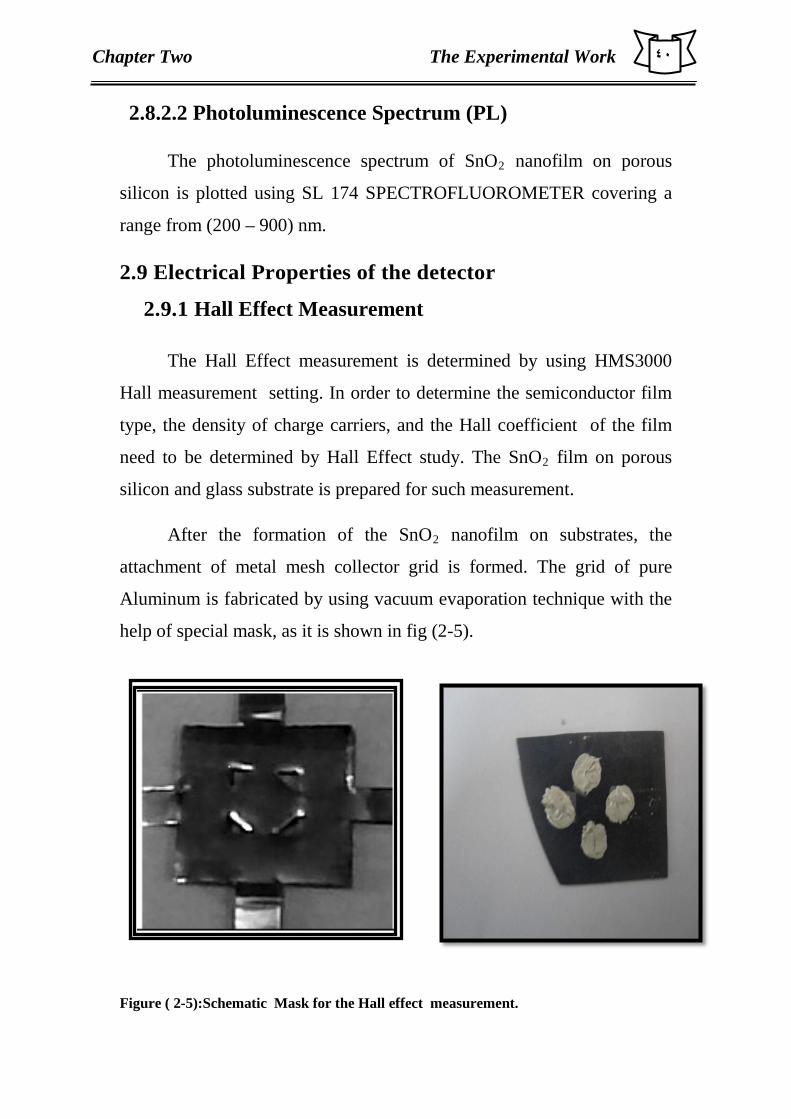
2.9.1 Hall Effect Measurement
The Hall Effect measurement is determined by using HMS3000
Hall measurement setting. In order to determine the semiconductor film
type, the density of charge carriers, and the Hall coefficient of the film
need to be determined by Hall Effect study. The SnOR2R film on porous
silicon and glass substrate is prepared for such measurement.
After the formation of the SnOR2R nanofilm on substrates, the
attachment of metal mesh collector grid is formed. The grid of pure
Aluminum is fabricated by using vacuum evaporation technique with the
help of special mask, as it is shown in fig (2-5).
Figure ( 2-5):Schematic Mask for the Hall effect measurement.

٤۱
Chapter Two The Experimental Work
An electrode must be on the surface of the SnOR2R nanofilm.
Aluminum which is an ohmic contact used as grid, the ohmic contact
made by evaporation of Aluminum under vacuum with the help of the
mask and this mask is fixed carefully on the surface of SnOR2R layer.
2.9.2 Detector Characteristic Measurement
In order to determine the detector parameters, mainly the
Responsivity , the response time and the specific detectivity ( DP
*P ) of the
fabricated SnO2 nanofilm on PS photoconductive UV detectors, a
suitable setup is prepared for this purpose. The system consists of:
HUIER DC power supply (ps-1502DD), variable resistance used to limit
the detector bias current , PC-interfaced digital Multimater, and Laptop
PC as shown in figure (2- 6). The UV – LED is used as a UV source for
illumination of the SnO2 photoconductive UV detector. The power of the
LED is 2.5mW and wavelength of about 385 nm and it is working with a
bais voltage of 5V, 11 mA.
The variation of photoresponsivity of SnOR2R sample and response
time of the prepared detector was tested by illumination the fabricated
detector with chopped UV-LED. The measuring circuit is shown in Fig
(2.7). The SnOR2R photocondutive detector output signal was displayed by
digital oscilloscope of 200 MHz model TDS 202413 from Tektronix.

٤۲
Chapter Two The Experimental Work
Figure ( 2-6): Schematic diagram of the experimental setup.
D.C. Power
Supply
Variable
Resistanc
UV-source SnO2-detector
PC – interfaced Digital Multimater
Laptop PC
USB interface
Cable
Optical Bench
A A D.C. Power
Supply
Variable
Digital Multimater
Rd

Chapter Three
Results and Discussion

٤۳
Chapter Three Results and Discussion
3.1 Introduction
This chapter presents the results and the analysis of the
experimental measurements of the SnOR2R films and the SnOR2R-UV
photoconductive detectors.
The results include the X-ray diffraction test, optical properties, and
photoconductive properties of SnOR2R films which are prepared by Sol-gel
method that has been tested.
Finally, the enhancement of the fabricating detectors by using
polymer is studied also chapter.
3.2 Structure Properties
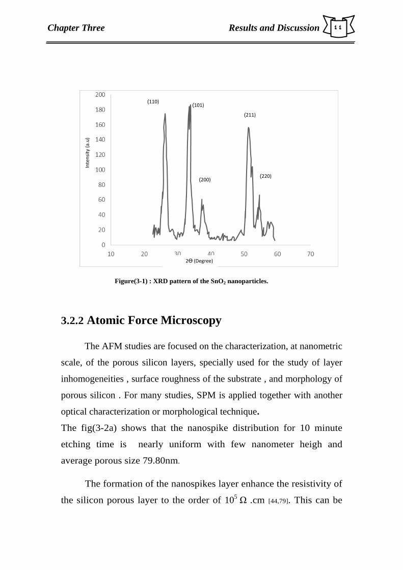
3.2.1 X-ray diffraction results of SnOR2R film
The X-ray diffraction (XRD) pattern of SnOR2R nanoparticles powder
is shown in Fig.(3-1) The peaks at 2θ values of 26.6°, 33.8°, 37.9°, 51.8°,
and 54.7° can be associated with (110), (101), (200), (211) and
(220)planes respectively. The SnOR2R product shows tetragonal structure,
which are in good agreement with other literatures. The average particle
size (D) was determined using the Scherer P
,Ps eq equation [ 78]:
1.3...........cosθβλKD =
1Twhere D is the crystallite size, K is the shape factor, being
equal to 0.9 , λ is the X-ray wavelength, β is the full width at half
maximum of the diffraction peak, and is the Bragg diffraction angle
in degree. The average particles size was found to be in the range of
8-10nm [74] .
٤٤
Chapter Three Results and Discussion
1T3.2.2 1TAtomic Force Microscopy
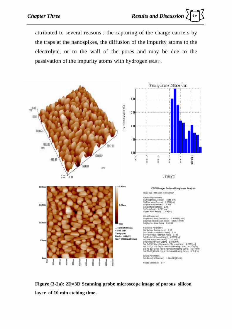
The AFM studies are focused on the characterization, at nanometric
scale, of the porous silicon layers, specially used for the study of layer
inhomogeneities , surface roughness of the substrate , and morphology of
porous silicon . For many studies, SPM is applied together with another
optical characterization or morphological technique.
1TThe fig(3-2a) shows that the nanospike distribution for 10 minute
etching time is nearly uniform with few nanometer heigh and
average porous size 79.80nm 1T.
1T The formation of the nanospikes layer enhance the resistivity of
the silicon porous layer to the order of 1T10P
5 PΩ1T .cm [44,79]. This can be
110)( 101)(
211)(
200)(
Inte
nsity
(a.u
)
220)(
2Ɵ (Degree)
Figure(3-1) : XRD pattern of the SnO2 nanoparticles.
٤٥
Chapter Three Results and Discussion
attributed to several reasons ; the capturing of the charge carriers by
the traps at the nanospikes, the diffusion of the impurity atoms to the
electrolyte, or to the wall of the pores and may be due to the
passivation of the impurity atoms with hydrogen [80,81].
1TFigure (3-2a): 2D×3D Scanning probe microscope image of porous silicon
layer of 10 min etching time.
٤٦
Chapter Three Results and Discussion
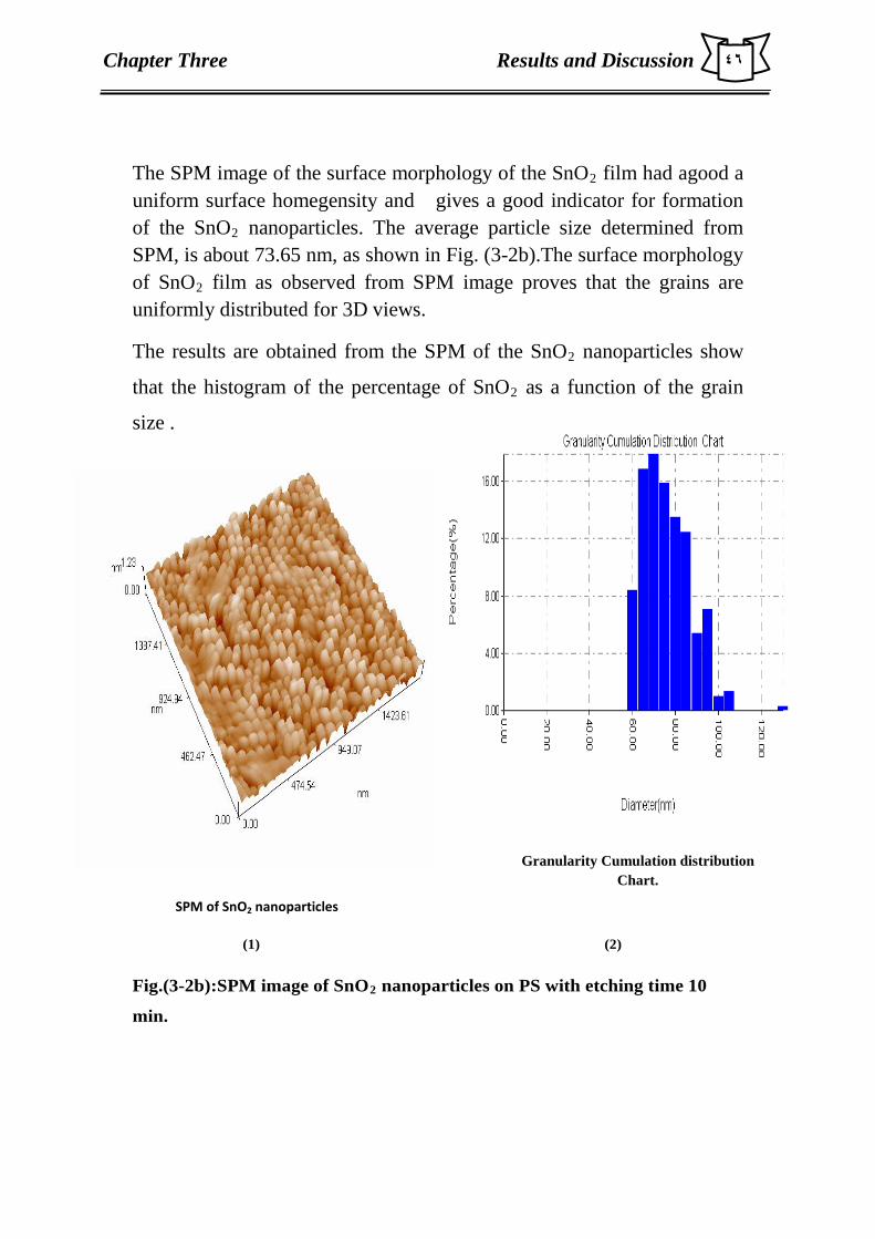
The SPM image of the surface morphology of the SnOR2R film had agood a uniform surface homegensity and gives a good indicator for formation of the SnOR2R nanoparticles. The average particle size determined from SPM, is about 73.65 nm, as shown in Fig. (3-2b).The surface morphology of SnOR2R film as observed from SPM image proves that the grains are uniformly distributed for 3D views.
The results are obtained from the SPM of the SnOR2R nanoparticles show
that the histogram of the percentage of SnOR2R as a function of the grain
size .
(1) 1T (2)
1TFig.(3-2b):SPM image of SnOR2R nanoparticles on PS with etching time 10
min.
Granularity Cumulation distribution Chart.
SPM of SnO2 nanoparticles
٤۷
Chapter Three Results and Discussion
0
0.5
1
1.5
2
2.5
3
250 300 350 400
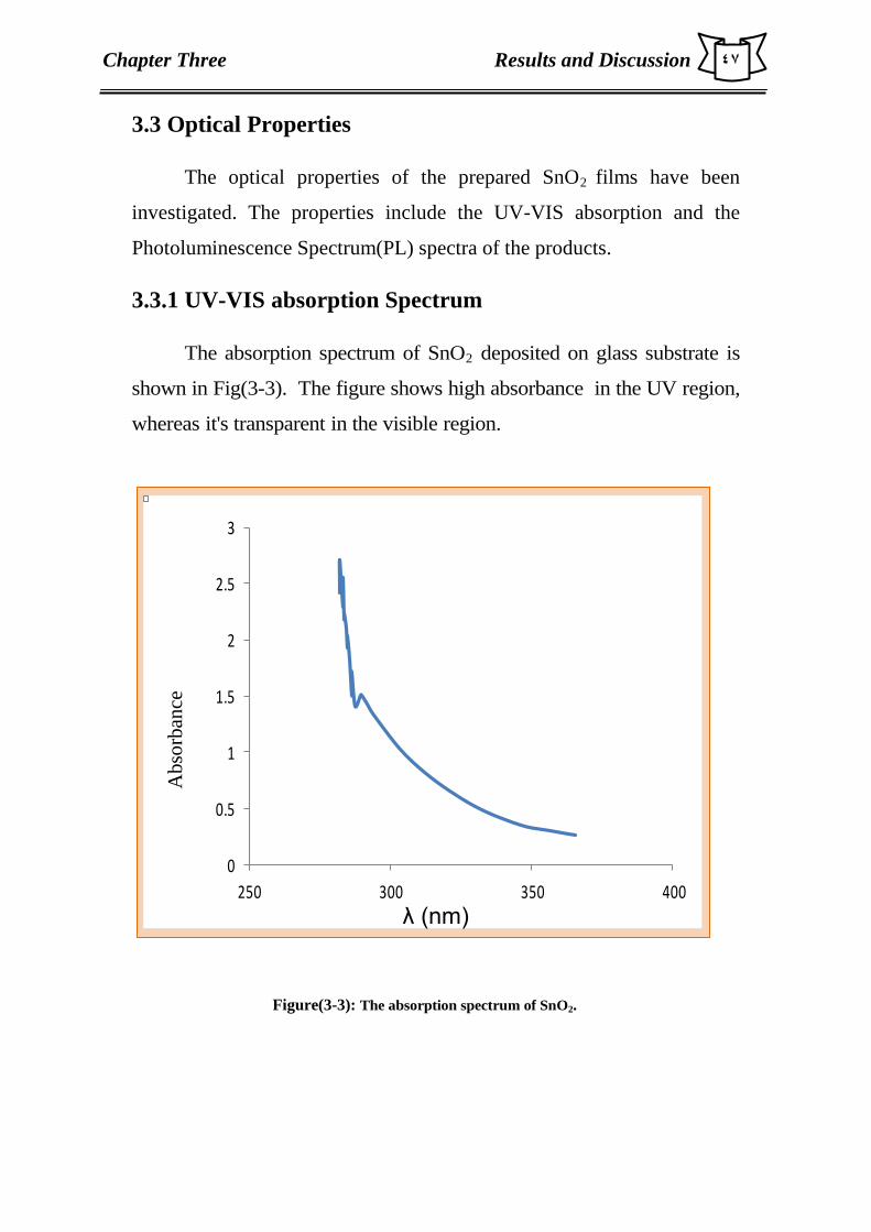
3.3 Optical Properties
The optical properties of the prepared SnOR2 Rfilms have been
investigated. The properties include the UV-VIS absorption and the
Photoluminescence Spectrum(PL) spectra of the products.
3.3.1 UV-VIS absorption Spectrum
1TThe absorption spectrum of SnOR2R deposited on glass substrate is
shown in Fig(3-3). The figure shows high absorbance in the UV region,
whereas it's transparent in the visible region.
λ (nm)
Abs
orba
nce
Figure(3-3): The absorption spectrum of SnO2.

٤۸
Chapter Three Results and Discussion
3.3.2 The energy band gap calculation The optical band gap energy (ERgR) of the semiconductor is calculated from
Tauc relation (2-3) [ 24]. A plot of (αhν)P
2 Pversus hυ shows intermediate
linear region, the extrapolation of the linear part can be used to calculate
the ERgR from intersect with hν axis as shown in Fig(3-4) .The resultant
values of ERgR for SnOR2R is found to be about 3.7eV and 4.3 eV[80] , 1TThe
above two values may be related to the formation of nanostructures of
SnOR2 Rand the bulk SnOR2R1T, these values show a good agreement with the
values published by other workers. [81,82].
Figure(3- 4) : Plot of (αhυ)2 versus photon energy (hυ) for SnO 2.

٤۹
Chapter Three Results and Discussion
3.3.3 The optical Photoluminescence spectrum The photoluminescence emission spectra of SnOR2 Rnanoparticles at
280nm excitation is shown in Fig (3-5).when 1TSnOR2R1T nanoparticles exhibit
emission at 437nm. The emission maximum of 437 nm is lower than the
band gap of SnOR2R bulk, this peak can be attributed to the contribution of
oxygen vacancies and defect in the 1TSnOR2R nanoparticles [83,81] 1T.
λ (nm)
Figure(3-5): Photoluminescence emission spectra of SnOR2.
1T3.4 Hall Measurements
1T The Hall measurements show 1Tthat the SnOR2R nanofilm deposited
on glass substrate is n-type semiconductor. The Hall parameters for n-
type nanofilms which included (resistivity, conductivity , and Hall
coefficient ) at etching time (10min) were illustrated in table (3-1).
Inte
nsity
(a.u
)

٥۰
Chapter Three Results and Discussion
Table (3-1): Hall effect parameters for SnOR2R film deposited on porous silicon.
3.033E+0 1TResistivity ( ρ )1T (Ω.cm)
3.297E-1 1TConductivity1T ( 1/ Ω cm)
-4.903E+1
1T Average Hall (mP
2P/c )
-1.273E+17 1TBUIK1T Concentration (cmP
-3 P) P
1.616E+1 1T/vs ) Mobility(μ )( cmP
2
3.5 The Photodetector Measurements
The photodetector measurements of the fabricated SnOR2R on PS -
UV photoconductive detector have been investigated. The measurements
include the I-V characteristics , the specific detectivity , the photocurrent
gain , and the response time.
3.5.1 I-V Characteristics
The current-voltage (I-V) characteristics of the fabricated device of
10 min etching time is illustrated in figure (3-6). The dark(IRdR) and
photo(Ip ) currents are increased with increasing the bias voltage. The
linear behavior may be related to the ohmic nature of the detector
sample. All samples used in the experiments of the photoresponsivity
measurements of the prepared detectors are carried out under identical
experimental conditions . The conditions are ; the distance between the
light source and the measured sample, the wavelength and the power of
the UV source , the area of the UV light incident on the sample, the
distance between the electrodes mask, and the applied bias voltage.
From the figure (3- 6 ) , it can be observed that the dark current is
very low under the illumination by visible light and the photocurrent is

٥۱
Chapter Three Results and Discussion
highly increased under the illumination by UV source with wavelength
385nm and 2.5 mW incident power.
Figure ( 3-6 ):The variation of the photocurrent of the fabricated SnOR2R UV detector on
porous silicon layer as a function of the bias voltage at etching time 10min.
The increase of the photocurrent of the polymer coated SnOR2R / PS
photoconductive UV detector samples are much higher than that of the
uncoated detectors samples as shown in fig (3-7).
0
20
40
60
80
100
120
140
160
0 1 2 3 4 5 6
I-dark+PS+SnO2
I-UV light+PS+SnO2

٥۲
Chapter Three Results and Discussion
Figure ( 3-7 ):The variation of the photocurrent of the fabricated SnOR2R UV detector on
porous silicon layer as a function of the bias voltage with coated polymer at etching time
10min.
1TFigure1T( 3-7 ) shows the variation of the photocurrent of the fabricated SnOR2R UV detector on porous silicon layer at etching time of 10min as a function of the bias voltage 1T.The dark current is found to be about 95µA at 5 V bias whereas the photocurrent is 251µA at the same bias votlage. This result reflects a good UV radiation sensitivity with photoconductive gain 1T(G) 1Tof more than 2.64.1T The photoconductve gain (G), which is calculated from the ratio between the photocurrent to the dark current at the same bias voltage, is given by the equation ( 1-8). Also ,the carrier life time (τ) was calculated after calculate TRr R(transit time), eq(1-9), using the values of G = 2.64, µ= 1.616×10 cmP
2P/ V.s as found from Hall
measurements, L = 0.04 cm and V = 5 V the carries life time (τ) was found to be about 50µs This result gives a good value for response time of the SnOR2R detector.
.

٥۳
Chapter Three Results and Discussion
3.5.2 The Specific Detectivity ( D*)
The specific detectivity D P
*P which is sometime called the
normalized detectivity , is the reciprocal of the Noise Equivalent Power
(NEP) normalized to the detector area of 1 cmP
2P and a noise of the
electrical band width ΔfR Ris 1 HZ.
1T This detector parameter is calculated for the fabricated
photodetector elements referring to equations; (1-12and1-16) , and
using the values of IRdR = 95 µA at the bias voltage of 5 V , 1TΔ1Tf = 1 Hz ,
photo responsivity RRλR = 0.1 A/W at λ=385nm, A = 1cmP
2P and IRnR = 5.561T
1T10P
-12PA , the specific detectivity of the fabricated SnOR2R UV detector
deposited on porous silicon layer is found to be 1.81T 1T10P
10 P cm.P
PHzP
1/2P.
WP
-1P.
3.5.3 Photocurrent Gain (G)
The photocurrent gain is calculated using equation (1-10) for the
polymer coated and uncoated SnOR2R UV photoconductive sample. The
average value of the gain registered for the polymer coated UV SnOR2R
photoconductive detectors under the same measurement conditions is
found to be about 2.64 , whereas the gain without polymer ≈ 2.2
The above value reflects the effect of the nylon polymer coating on
the improvement of the gain of the fabricated detector.
Since the photoelectric current gain (G) is a function of electrodes
geometry. Thus the photoelectric gain can highly be improved by
reducing the electrodes spacing P
P[84].
×
×
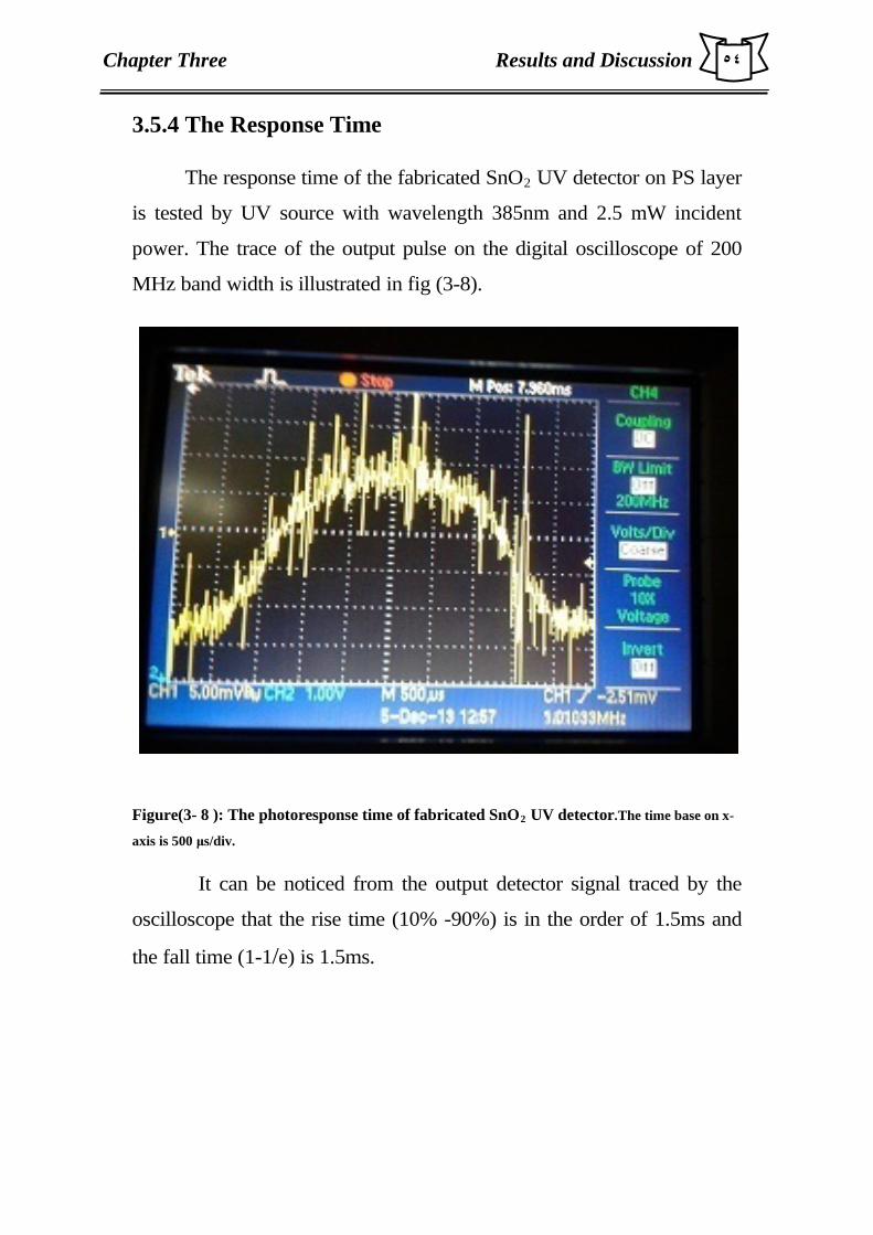
٥٤
Chapter Three Results and Discussion
3.5.4 The Response Time
1TThe response time of the fabricated SnOR2R UV detector on PS layer
is tested by UV source1T with wavelength 385nm and 2.5 mW incident
power 1T. The trace of the output pulse on the digital oscilloscope of 200
MHz band width is illustrated in fig (3-8).
Figure(3- 8 ): The photoresponse time of fabricated SnOR2R UV detector1T.The time base on x-
axis is 500 μs/div.
1T It can be noticed from the output detector signal traced by the
oscilloscope that the rise time (10% -90%) is in the order of 1.5ms and
the fall time (1-1/e) is 1.5ms.

٥٥
Chapter Three Results and Discussion
3.6 Conclusion
1-The SnOR2R UV photoconductive detector samples prepared by Sol
gel method are fabricated, which indicate that the Sol gel method can be
considered as a good method to prepare SnOR2R nanopowder for the UV
detectors.
2- The PL spectrum of SnOR2R shows that excitation at 280nm, 1TSnOR2R1T
nanoparticles exhibit emission at 437nm. The emission maximum of 437
nm is lower than the band gap of the SnOR2R bulk, this peak can be
attributed to the contribution of oxygen vacancies and defect in the 1TSnOR2R
nanoparticles1T.
3- The functionalization of the SnOR2R samples surface by polymers
shows giant enhancement in the photoresponsivity.
4- The maximum responsivity was observed by the samples coated with the Polyamide nylon and it is about 0.1 A/watt and response time was about 50µs.
.
3.7 Suggestions of future work
According to our results, the following ideas are suggested
1-Synthesis SnOR2R samples is by using other techniques such as
pulse laser deposition technique on silicon substrate to improve
the quality of the film and to enhance the detector performance.
2- Doping prepared SnOR2 R with other material like fluorine and
Carbon nanotube to improve the response time and the
responsivity of the detector.

٥٦
References
1. Rozália Szentgyörgyvölgyi, "Properties of Paper Substrates Made with
Nanotechnology", Óbuda University, Vol. 1,No. 1, PP.227-235,2010.
2.GE Aninwene, CY II, TJ Webster ,"Nanomedicine",J.Intermational,Vol.
3(2),PP.257-264,2008.
3. Ulrika Backman, "Studies on nanoparticles synthesis via gas-to-particle
conversion", Faculty of Science, University of Helsinki ,2005.
4. Muhammad Raffi,"synthesis and Characterizaton of metal
Nanoparticles"Department of Chemical and Materials Engineering", Ph.D,VDM
Verlag, 2007.
5.Taylor, Alicia A, ," CARBON AND CLAY NANOPARTICLES PROVOKE NUMEROUS
REPSONSES IN SALMONELLA ENTERICA VAR", TYPHIMURIUM AND ESCHERICHIA
COLI",M.Ss, Dept of Biology, University-San Marcos,2010.
6. Kewei Wang, "NANOMATERIALS:FROM INTERFACIAL ARACTERISTICS
TO DEVICEAPPLICATIONS" Ph.D. Thesis, Department of Materials Science &
Hamilton, McMaster University,(2012).
7. Ake Thidell ,Peter Arnfalk," Nanoparticles: A Closer Look at the Risks to
Human Health and the Environment" Master of Science in Environmental
Management and Policy Lund, 2004 .
8.Haidar Hameed Hamdan, “Fabrication of TiOR2 RNanotube Using Electrochemical
Anodization” , College of Science, University of Baghdad, College of Science,
University of Baghdad,M.Ss,2012
9. 6TB S Murty6T, 6TP Shankar6T,1T 1T 6TBaldev Raj 6T,1T 1T 6TB B Rath6T,1T 1T 6TJames Murday6 T, "Unique
Properties of Nanomaterials",Springer Berlin Heidelberg1T, 1Tpp. 29-65,2013.
10. V.V. Pokropivny,V.V. Skorokhod,"Classification of nanostructures by
dimensionality and concept of surface forms engineering in nanomaterial
science", Elsevier, Amsterdam ,Vol. 27, Pp 990–993,2007.
11. Paul Harrison, "Quantum Wells, Wires and Dots: Theoretical and
Computational Physics", Wiley and Sons, New York 2000.
12. Jody Erickson," Incorprating Carbon Nanotubes in to Polyropylene Fibers",
M.Sc.,thesis, North Carolina State University, 2003.
13. Osama Natak Najy," Effect of Carbon Nanotubes on the Properties of Liquid
Crystal" , Ph .D, College of Science,University of Baghdad, , 2009.

٥۷
References
14.F.F. Komarov , A.M. Mironov " ,Carbon Nanotubes : Present and Future",
Physics and Chemistry of Solid State, Vol.5, No.3,pp.411-429, 2004.
1155..HHiinndd IIbbrraahhiimm MMuurraadd, "" SSuurrffaaccee PPllaassmmoonn aanndd OOrrggaanniicc SScciinnttiillllaattoorrss
Enhancement of The White Light Emission From CdSe/ZnS Core- Shell",M.Sc,
College of Science, University of Baghdad, 2012.
16.Reem Rafaa Mohamed, "Enhancement of the photovoltaic solar cell efficiency
by nanoscintillators core-shell system", M.Sc, College of Science, University of
Baghdad, 2010.
17.Smritimala Sarmah, A. Kumar,"Optical properties of SnOR2R Nanoparticles" , J.
Physics,Vol. 84, pp 1211-1221, ,2010.
18.zur Erlangung des Grades,"Tin (IV) Oxide Nanostructures:Controlled
SynthesisProperties and Applications in Dye-Sensitized Solar
Cells",Ph.D,University of Mainz and the Seoul National University,2010.
19.Khalid K. Mohammed," The Electrical and Optical Properties of SnO2–
Si(n)Structure Solar Cells",Electrical Engineering Department – University of
Mosul, J.Al-Rafidain Engineering ,Vol.13, No.3, 2005.
20.6TJ.X. Zhou 6T,1T 1T6TM.S. Zhang6T,1T 1T6TJ.M. Hong6T, 6TJ.L. Fang6T,1T 1T6TZ. Yin6T,"Structural and spectral
properties of SnO R2 Rnanocrystal prepared by microemulsion
technique",Metarial ScienceαProcessing,Vol.81, pp .177-182,2005.
21. S. GNANAM, V. RAJENDRAN ," LUMINESCENCE PROPERTIES OF EG-ASSISTED
SnO2 NANOPARTIC,LES BY SOL-GEL PROCESS", College of Presidency, India, Vol.
5, No 3, pp. 925 – 930, J. Nanomaterials and Biostructures, 2010.
22.Martin Sinner-Hettenbach," SnO2(110) and Nano-SnO2: Characterization by
Surface Analytical Techniques" Ph.D,Universit¨at T¨ubingen, 2000.
23. K.Vadivel, V.Arivazhagan, S.Rajesh," Mn DOPED SnO2 Semiconducting
Magnetic Thin Films Prepared by Spray Pyrolysis Method", J .Scientificα
Engineering,Vol. 2,PP.1-5, 2011.
24. A. SHARMA, D. PRAKAHa, K. D. VERMA," Post annealing effect on SnO2 thin
films grown bythermal evaporation technique", S.V.College, , Aligarh (U.P.)
India, Vol. 1, No. 12, Pp. 683 – 688,2007.
25. Min-Sik Park, 1T 1TGuo-Xiu Wang,1T 1TYong-Mook Kang,1T 1TDavid Wexler, 1T 1TShi-Xue Dou
Prof,1T 1THua-Kun Liu Prof"10T Preparation and Electrochemical Properties of
٥۸
References
SnOR2R1T10T 1T10TNanowires for Application in Lithium-Ion Batteries 10T",6TVol.119,6TPp .764–767,1T 1T
2007.
26. Lian Ee Khoo, Zhao-Hui Zhou, Thomas C. W. Mak," Crystal and molecular
structure of dimeric bis[dibutyl(2-hydroxyphenylmethylimino-β-
alaninato)tin] oxide",J.Crystallographic α spectroscopic research, Vol. 23, pp
153-157,1993.
27.Rusen Yang and Zhong Lin Wang" Springs, Rings, and Spirals of Rutile-
Structured Tin Oxide Nanobelts", J. AM. CHEM. SOC. 9 VOL. 128, NO. 5, 2006 .
28. Richard Rivera, Freddy Marcillo, Washington Chamba, Patricio Puchaicela,
Arvids Stashans," SnO2 Physical and Chemical Properties due tothe Impurity
Doping", Proceedings of the International MultiConference of Engineers and
Computer Scientists, HongKong, VOL.NO.11, 2013.
29. Mihaiu Maria Susana, Scarlat Oana, Zuca Stefania ,Zaharescu Maria," Advanced
SnO2-Based Ceramics Synthesis, Structure, Properties", Institute of Physical
Chemsitry of the Romanian Academy,2011.
30.Anima Johari, M. C. Bhatnagar , Vikas Rana1 ,"Growth, characterization and I-
V characteristics of tin oxide (SnOR2R) nanowires", J. ADVANCED MATERIALS,
Physics Department,NewDelhi 110016, India,VOL.3(6),PP. 515-518,2012.
31. Zhiwen Chen,a) J.K.L. Lai, C.H. Shek, and Haydn Chen," Synthesis and
structural characterization of rutileSnO2 nanocrystals", J. Materials, Department
of Physics and Materials Science, University of Hong Kong, Vol. 18, pp. 1289-
12921T, 1T2003.
32. K. ANANDAN, V. RAJENDRAN ,"SIZE CONTROLLED SYNTHESIS OF SnOR2
RNANOPARTICLES FACILE SOLVOTHERMAL PROCESS " J. Non-Oxide Glasses.
Vol. 2, No. 2 , PP. 83 – 89, 2010.
33. 6TMadzlan Aziz 6T, 6TSaad Saber Abbas 6T,1T 1TWan Rosemaria, Wan Baharom , "Size-
controlled synthesis of SnOR2R1T 1Tnanoparticles by sol–gel method, Faculty of
Science", J. Materials Letters, VOL.91, PP. 31–34, 2013.
34. Matthias Batzill,Ulrike Diebold , "The surface and materials science of tin
oxide", J.Progress in Surface Science,VOL.79, PP. 47-154 , 2005.
1T 1T35. 6TP.R. Bueno6TP
,,P6TP
PE.R. Leite6T,6T L.O.S. Bulhões 6T, 6TE. Longo6T,6T C.O. Paiva-Santos 6T, "Sintering
and mass transport features of (Sn,Ti)OR2R6T 6Tpolycrystalline ceramics", 1TJ. European
Ceramic Society 1TVOL.23, PP. 887–896, 2003.1T
٥۹
References
36. A. Ayeshamariam ,"Synthesis, Structural and Optical Characterizations of
SnO2 Nanoparticles", Journal on Photonics α Spintronics Vol.2 ,2013.
37. S. Thanasanvorakun, P. Mangkorntong, S. Choopun, N. Mangkorntong,
"Characterization of SnO2 nanowires synthesized from SnO by carbothermal
reduction process",CeramicsInternationaL,vol.34,pp.1127-1130,2008.
38.Myung Sub Kim, Hee Kwan Lee, Jae Su Yu ," Electrochemically controlled
synthesis and characterization of SnO2 nanostructures on FTO glass
substrate",Department of Electronics and Radio Engineering, Kyung Hee
University, 2012.
39.Hanan AbdAli Thjeel,:"" FFaabbrriiccaattiioonn aanndd CChhaarraacctteerriizzaattiioonn ooff ZZnnOO//PPoorroouuss Si
Photoconductive UV Detector",M.Ss, College of Science, University of
Baghdad,2011.
40.Fatin Emad Naoum," Preparation of Si/ZnO Junction for UV Detection"
M.Ss,College of Science, University of Baghdad, 2009.
41.Hasan Hadi Hussein ,"Study of the Characteristics of Porous Silicon by
Electrochemical Etching", College of Science, University of Baghdad , Vol.31,
No.1,J. Eng. & Tech, pp. 900-909 , 2013.
42.Y L Liu, Y C Liu , H Yang, W B Wang, J G Ma, J Y Zhang, Y M Lu, D Z
Shen1T 1Tand X W Fan P
,P "The optical properties of ZnO films grown on porous Si
templates", J. Physics Dvol VOL. 36,NO.21,2003.
43. H. Mavi, B. Rasheed, A. Shukla, S. Abbi, and K. P. Jain, " Spectroscopic
Investigations of Porous Silicon Prepared by Laser – Induced Etching of Silicon,
" J. Phys., Vol. 34, pp. 1-7,2001.
44. A. Alwan , "Silicon Nano – Crystallites Produced by Photochemical Etching",
Ph. D. Thesis, Sch. of Appl. Sci., University of Technology, 2006 .
45. Hassan A. Kadhim ,"Preparation and study of porous Silicon layers from n-
type Silicon wafers using different etching techniques ",Ph.D. Thesis , University
of Baghdad, Dep. Of Physics,2009.
46. 6TNaokatsu Yamamoto 6T, 6THiroshi Takai 6T,1T" 1TFormation mechanism of silicon based
luminescence material using a photo chemical etching method", Elsevier
,vol.388,pp.138-142,2001.
47.6TTakehito Senga6T11T,1T11T 1T6TYutaka Matsumi 6T11T and1T11T 1T6TMasahiro Kawasaki 6T,1T 1T19TVIEW
AFFILIATIONS 19T ,"Chemical dry etching mechanisms of GaAs surface by HCl
and ClR2R", J. Vacuum,VOL.14,PP. 43230 - 3238,2009.

٦۰
References
48.S. Affrossman, R. T. Bailey, C. H. Cramer, F. R. Cruickshank, J. M. R. acAllister,
J.Material science ,"Laser photochemical etching of ilicon",vol.49,pp.533-542,
,1989.
49.F.V. Mikulec ,J.D. Kirtland,1T 1TM.J. Sailor ,"Oxide‐free blue photoluminescence
from photochemically etched porous silicon" 1TJ. 1T6TApplied Physics
Letters 6T.1T 1T6TVol.69,1996 6T.
50.17THummel, R.E. 17T "Novel technique for reparing porous silicon", Department of
Materials Science and Engineering, University of Florida, Vol.61,PP. 1965 – 1967
51.R. Menzel, "Photonics", Springer, Berlin,2001.
52. Jack Ready ," Optical Detectors and Human Vision",1991.
53. A. ROGALSKI, " Optical Detectors for focal arrays", OPTO-ELECTRONICS
REVIEW ,vol.12(2),pp. 221–245, 2004.
54. George Rieke," Detection of Light: From the Ultraviolet to the Submillimeter",
Cambridge University Press, 2003. 55. P. R . Norton,Photodetectores", Handbook of Optics Santa Barbara Research
Center, Santa Barbara , California ,Vol,ch. 15 pp. 5- 1, 2000.
56.Eman Kareem Hassan,, ""PPrreeppaarraattiioonn aanndd DDeevveellooppmmeenntt ooff PPoollyymmeerr CCooaatteedd ZZiinncc
OOxxiiddeeFFiillmmss ffoorr UUVV-- DDeetteeccttiioonn",M.Sc,College of Science, University of
Baghdad,M.Ss,2010.
57. Emman M. Nasir , " Fabrication of CdSe:Cu Photoconductive Detector by
using vacuum Evaporation Technique and studing its Electro-Optical
Properties", M.Sc. Thesis , University of Baghdad , Dep. Of Physics ,1999.
58.Cesare Soci, Arthur Zhang, Xin-Yu Bao, Hongkwon Kim, Yuhwa Lo, and Deli
Wang,"Nanowire Photodetectors",J .Nanoscienceand Nanotechnology,Vol.10,pp.1–
20, 2010 .
59. Bryant Conant," The Chemistry of organic compounds", Japan, 1961.
60. Ghusson H. Mohammed, “Optoelectronic Parameters Of PbRXRSR1-XR Thin Films",
M.Sc, University of Baghdad, Dep. Of Physics ,2002.
61. N.V.Joshi,"Photoconductivity"ART,SCIENCE,AND TECHNOLOGY,1992.
62.Iman H.Khdayer ," Fabrication and studying the photoconducting
characteristics of InSb Junction with silicon as asigle crystal semiconductor "
Ph.D , University of Baghdad, Dep. Of Physics,2005.

٦۱
References
63.RICHARD.H.BUBE,"Photoelectronic properties of Semiconductors",
Cambridg university press,1992.
64. A.M.Suhail, " The analysis of uncooled solar blind ZnO Photoconductive
detector ", private communication.
65. Feng Gu, Shu Fen Wang , Chun Feng Son g, Meng Kai L€u, Yong Xin Qi,
Guang Jun Zhou, Dong Xu , Duo Rong Yuan,"Synthesis and luminescence
properties of SnO2 nanoparticles",Chemical Physics letters,2003.
. 66.SANJAY R DHAGE, S P GAIKWAD, VIOLET SAMUEL and V RAVI ,"Synthesis of
nanocrystalline SnO2 powder at 100°C", Physical and Materials Chemistry
Division, National Chemical Laboratory,Vol. 27, No. 3 ,pp. 221–222, 2004.
67. J.J. Valenzuela-Ja uregui, R. Quintero-Gonza lez, J. Herna ndez-Torres, A.
Mendoza-Galva n, R. Ramı rez-Bon," Characterization of SnO2, In2O3, and ITO
films prepared by thermal oxidation of DC-sputtered Sn, In and In–Sn films",
VOL. 76 ,PP.177–180,2004.
68.Luhua Jiang, Gongquan Sun, Zhenhua Zhou, Shiguo Sun, Qi Wang, Shiyou
Yan,Huanqiao Li, Juan Tian, Junsong Guo, Bing Zhou, and Qin Xin," Size-
Controllable Synthesis of Monodispersed SnO2 Nanoparticles and Application in
Electrocatalysts",VOL. 109, PP8774-8778,J. Phys. Chem. , 2005.
69.Chunjoong Kim, Mijung Noh, Myungsuk Choi, Jaephil Cho, Byungwoo
Park,Chem. Mater ,"Critical Size of a Nano SnO2 Electrode for Li-Secondary
Battery", VOL.17, PP.3297-3301, 2005.
70. M.-M. Bagheri-Mohagheghia,b, N. Shahtahmasebia, M.R. Alinejada,A.
Youssefic, M. Shokooh-Saremi," The effect of the post-annealing temperature
on the nano-structure and energy band gap of SnO2 semiconducting oxide nano-
particles synthesized by polymerizing–complexing sol–gel method Physica",PP.
2431–2437,2008.
71.S . MAJUMDER ," Synthesis and characterisation of SnO2 filmsobtained by
a wet chemical process", J. Materials Science-Poland, Vol. 27, No. 1, 2009.
72. Rohana Adnan, Nur Ariesma Razana, Ismail Abdul Rahman , Muhammad Akhyar
Farrukh,"Nanoparticles via the Sol-Gel Method as a Catalyst for the Synthesis
and haracterization of High Surface Area Tin Oxide Hydrogenation of Styrene",
J. Chinese Chemical Society, VOL.57, PP.222-229, 2010.
٦۲
References
73. Lucky M Sikhwivhilu, Sreejarani K Pillai1, Thembela K Hillie1,"Influence of
Citric Acid on SnO2 Nanoparticles Synthesized by Wet Chemical Processes",
J.Nanoscience α Nanotechnology ,Vol . 11, No. 6, pp. 4988-4994(7), 2011 .
74. L. C. Nehru, V. Swaminathan, C. Sanjeeviraja, "Photoluminescence Studies on
Nanocrystalline Tin Oxide Powder for Optoelectronic Devices" , J.American of
Materials Science,Vol.2,No.2,pp.6-10, 2012.
75. Ganesh E Patil, Dnyaneshwar D Kajale, Vishwas B Gaikwad1 , Gotan H Jain,
"Preparation and characterization of SnO R2 Rnanoparticles by hydrothermal
route",VOL.2,NO.17,2012.
76. Pankov JI," Optical Processes in Semiconductors",Dover ,1971.
77.S.M.Sze α Kwok K.Ng, " Physics of Semiconductor Devices", Third Edition ",
John Wiley α Sons, New York,(2007).
78. Cullity, B.D," Elements of X-ray Diffraction". Boston, Addison-
Wesley,Publishing Co, 1956.
79. Algun and M. Arikan , " An Investigation of Electrical Properties of Porous
Silicon " , J. Tr of Physics , Vol. 23 , pp. 789 – 797 , 1999.
80. G. Smetad, M. Kunst and C. Vial, "photovoltaic response in electrochemically
prepared photoluminescent porous silicon", Solar Energy Materials α Solar Cells,
Vol. 26, pp:277 – 283,1992.
81. W. T. Hsieh, Y. K. Fang, K. H. Lee, J. J. Ho , C. W. Ho, "Using Porous silicon
as SiC High Temperature Optical –Sensing Devices", IEEE Transactions on
Electron Devices,Vol. 48, pp. 801 – 803,2001.
82. A.M.Suhail , N.N.Jandow α K.Ibrahim ," The Optical Properties of ZnO
Thin Film on plastic Substrate by DC-Sputtering", Proceeding 3P
rdPscientific
conference of the college of Science, University of Baghdad, pp. 24-26 ,2009.
83.Y.Wang and N.Herron ,"Nonometer-Sized Semiconductor Clusters: Materials
Synthesis, Quantum Size Effects ,and photophysical Properties",
J.Phys.Chem.,Vol.95,pp:525-532(1991.
84. Jun Zhou, Yudong Gu, Youfan Hu, Wenjie Mai, Ping-Hung Yeh , Gang Bao,
Ashok K.Sood, Dennis L. Polla and Zhong Lin Wang ," Gigantic enhancement in
response and reset time of ZnO UV nanosensor by utilizing Schottky contact and
surface functionalization ", Applied Physics Letters , Vol. 94, pp. 191-103, 2009.


ISSN: 2319-8753
International Journal of Innovative Research in
Science,Engineering and Technology
(An ISO 3297: 2007 Certified Organization)
Vol. 2, Issue 12, December 2013
7068 www.ijirset.com yright to IJIRSETCop
Preparation and Characterization of SnO2
Nanoparticles Asama. N. Naje1 , Azhar S.Norry2, Abdulla. M. Suhail3
Lecture, Dept. of Physics , College of Science, University of Baghdad, Baghdad, Iraq1
M.Sc. student, Dept. of Physics , College of Science, University of Baghdad, Baghdad , Iraq2
Asst. Prof., Dept. of Physics , College of Science, University of Baghdad, Baghdad, Iraq, Dept of Optometry, Dijlah
University college, Baghdad, Iraq3
Abstract: Tin Oxide (SnO2) nanoparticles powder have been synthesized by chemical precipitation method. The samples were characterized by X-ray diffraction, UV-Visible absorption and scanning probe Microscope SPM. The X-ray analysis shows that the obtained powder is SnO2 with tetragonal rutile crystalline structure and the crystalline size in the range of 8-10nm. The SPM investigation reveals that the average particles size is 73nm. The optical band gap values of SnO2 nanoparticles were calculated to be about 4.3eV in the temperature 550 o C, comparing with that of the bulk SnO2 3.78eV, by optical absorption measurement.
Keywords: SnO2 nanoparticles, X-ray diffraction ,Morphology, Optical Properties.
I. INTRODUCTION
Nanometer-sized materials have recently attracted a considerable amount of attention due to their unique electrical, physical, chemical, and magnetic properties, these materials behave differently from bulk semiconductors. With decreasing particle size the band structure of the semiconductor changes; the band gap increases and the edges of the bands splits into discrete energy levels. These so-called quantum size effects occur [1-5]. These quantum size effects have stimulated great interest in both basic and applied research.
Tin oxide (SnO2) is one of the most intriguing materials to be investigated today, This is because tin dioxide is a well-known n-type semiconductor with a wide band gap of 3.6-3.8 eV [ 6-8], and for its potential application in transparent conductive electrode for solar cells a gas sensing material for gas sensors devices, transparent conducting electrodes, photochemical and photoconductive devices in liquid crystal display , gas discharge display, lithium-ion batteries, etc[9- 14 ]. Many processes have been developed to the synthesis of SnO2 nanostructures, e.g., spray pyrolysis, hydrothermal methods, chemical vapor deposition, thermal evaporation of oxide powders and sol–gel method [15-20 ]
In the present work the fabrication and characterization of crystalline SnO2 nanoparticles powder by chemical precipitation method was studied
II. EXPERIMENTAL WORK
SnO2 nanopowders were prepared by means of dissolving of 2 g (0.1 M) stannous chloride dehydrate (SnCl2.2H2O) in 100 ml distilled water. After complete dissolution, ammonia solution was added to the above solution by drop wise under stirring. The resulting gels were filtered and dried at 80ºC for 24 hours in order to remove water molecules. Finally, tin oxide nanopowders were formed at 550ºC for 2h.
The obtained samples were characterized by X-ray powder diffraction (XRD) using (XRD -6000), supplied by SHIMADZU. The surface morphology of the samples was observed by Scanning probe Microscope (SPM) by using CSPM AA3000, supply by Angstrom Company. Optical absorption spectra of the samples were taken with OPTIMA SP-3000 UV-VIS Spectrometer,. The room temperature photoluminescence (PL) spectra of SnO2 were recorded with SL 174 SPECTRFLUORMETER.

الخالصهفي هذه الدراسة تم تصنيع كاشف التوصيل الضوئي لألشعة فوق البنفسجية من المسحوق النانوي
اوكسيد القصدير المحضر بالطريقة الكيماوية ورسب المسحوق على الزجاج والسيلكون المسامي
ة بطريقة الطالء بالتغميس ، ثم اجريت الفحوصات التركيب المحضر بطريقة التنميش الضوئي
والسطحية والخصائص البصرية للعينات المحضرة.
تم فحص المسحوق النانوي اوكسيد القصدير بواسطة حيود االشعة السينية ووجد ان تركيبها
). 110,101متعدد البلورات ذات تركيب رباعي الزاويا مع اتجاهية بلورية عالية عند (
لمرسبه على لزجاج فجوات طاقه الدراسات البصرية ان الغشية اوكسيد القصدير ا وأظهرت
.437nmاثية عند طول موجي .ما طيف االنبعاث اظهر انبع 4.37e Vو 3.7eVمقدارها
بينت دراسة شكل السطح للمسحوق النانوي المرسب عل السيلكون ان معدل الحجم الحبيبي هو
73.65nm.
الجهد في حالة الظالم -من خالل التيار كتم دراسة الخواص الكشفية للكاشف المحضر وذل
بينت وكما 385nmوبطول موجي mW 2.5لدايود االشعة فوق البنفسجية ذو قدرة واألضاءة
.n-typeقياسات هول ان المسحوق النانوي المرسب على السيلكون السامي هو من نوع
بوليمر بنوع من ال اخيرا تم معاملة سطح اوكسيد القصدير المرسب على السيلكون المسامي
)polyamide nylon 0.1) لتحسين استجابية الكاشف الىA/W ثم تم قياس زمن االستجابة
وسجلت اشارة نبضة الخرج باالسيلسكوب الرقمي. 0.052msللكاشف المصنع وسجل قيمة

جمهورية العراق
وزارة التعليم العالي والبحث العلمي
كلية العلوم\جامعة بغداد
تصنيع ودراسة كاشف التوصيل الضوئي اوكسيد القصدير لألشعة فوق البنفسجية
رسالة مقدمة الى
جامعة بغداد–كلية العلوم
كجزء من متطلبات نيل درجة الماجستير
في الفيزياء
من قبل
شاكر نوري غافلازهار )۱۹۹٤اء ي(بكالوريوس علوم في الفيز
أشراف
د.عبد أل محسن سهيل أ.
م.د.أسامة ناطق ناجي ـه۱٤۳٥م ۲۰۱٤
Related Documents


