FABRICATION AND PERFORMANCE CHARACTERIZATION OF PET/ITO/ZNO NANOROD/P3HT:PCBM AND PET/ITO/P3HT:PCBM SOLAR CELL IZZATI HUSNA BINTI ISMAIL UNIVERSITI SAINS MALAYSIA 2015

Welcome message from author
This document is posted to help you gain knowledge. Please leave a comment to let me know what you think about it! Share it to your friends and learn new things together.
Transcript

FABRICATION AND PERFORMANCE
CHARACTERIZATION OF PET/ITO/ZNO
NANOROD/P3HT:PCBM AND
PET/ITO/P3HT:PCBM SOLAR CELL
IZZATI HUSNA BINTI ISMAIL
UNIVERSITI SAINS MALAYSIA
2015

FABRICATION AND PERFORMANCE
CHARACTERIZATION OF PET/ITO/ZNO
NANOROD/P3HT:PCBM AND
PET/ITO/P3HT:PCBM SOLAR CELL
by
IZZATI HUSNA BINTI ISMAIL
Thesis submitted in fulfilment of the requirements
for the degree of Master of Science

ii
ACKNOWLEDGEMENT
First of all, I would like to express my thanks to my main supervisor,
Professor Kamarulazizi bin Ibrahim for his excellent guidance and concern
throughout the entire research. Secondly, I would like to acknowledge my co-
supervisor, Dr. Melati binti Khairuddean from School of Chemistry who offered me
the opportunity to boost and improve my knowledge in the field of organic polymer
material.
I feel greatly thankful to the entire lab assistant in NOR laboratory for their
contribution and support all the time in my research studies. Additionally, I’m
indebted and thankful to the USM for offering me USM scholarship to ease my
financial burden during my research study. Last but not least, I would like to thank
my beloved family and friends for giving me the motivation and inspiration to
complete my research study.

iii
TABLE OF CONTENTS
PAGE
ACKNOWLEDGEMENT ii
TABLE OF CONTENTS iii
LIST OF FIGURES vii
LIST OF TABLE x
LIST OF SYMBOL xi
LIST OF ABBREVIATIONS xiii
ABSTRAK xiv
ABSTRACT xvi
CHAPTER 1: INTRODUCTION
1.1 Background of study 1
1.2 Problem Statement 3
1.3 Objectives 3
1.4 Originality of the research work 4
1.5 Thesis outline 4
CHAPTER 2: LITERATURE REVIEW
2.1 The history of solar cells - from inorganic to organic 6
2.2 Comparison between generations of solar cell 9
2.3 Basic working principle of organic photovoltaic 9
2.4 Bulk heterojunction and hybrid (ordered) 13
heterojunction solar cell architectures

iv
2.4.1 Bulk heterojunction 13
2.4.2 Ordered heterojunction (hybrid) 14
2.5 Poly(3-hexylthiophene) (P3HT) 16
2.6 Electron-acceptor material 17
2.6.1 Methanofullerene Phenyl-C61-Butryic-Acid-Methyl-Ester 17
(PCBM)
2.6.2 Zinc Oxide (ZnO) nanorod 18
2.7 Buffer layer 18
2.7.1 PEDOT:PSS 18
CHAPTER 3: METHODOLOGY
3.1 Materials 20
3.2 Instrument and characterization 20
3.2.1 Nuclear Magnetic Resonance (NMR) Spectroscopy 21
3.2.2 Fourier Transfer Infrared (FTIR) 22
3.2.3 Ultraviolet-visible (UV-VIS) spectrophotometer 23
3.2.4 Field Emission Scanning Electron Microscope (FESEM) 24
3.2.5 X-Ray Diffraction (XRD) 24
3.2.6 Solar simulator 25
3.2.7 Spin coating 28
3.2.8 Microwave oven 29
3.3 Production procedure 29
3.3.1 Preparation of substrates 29
3.3.2 P3HT synthesis 30
3.3.3 Preparation of bulk heterojunction device (organic solar cell) 31

v
3.3.4 Preparation of ordered heterojunction device (hybrid solar cell) 32
CHAPTER 4: RESULTS AND DISCUSSION OF HYBRID SOLAR CELL
4.1 Synthesis and characterization of ZnO nanorod 34
4.1.1 Synthesis of ZnO nanorod 34
4.1.2 FESEM analysis 35
4.1.3 XRD analysis 39
4.1.4 UV-VIS analysis 41
4.2 Characterization of ZnO nanorod/P3HT and 42
ZnO nanorod/P3HT:PCBM
4.2.1 FESEM analysis 42
4.2.2 UV-VIS analysis 46
4.2.3 Solar simulator analysis 48
CHAPTER 5: RESULTS AND DISCUSSION OF ORGANIC SOLAR CELL
5.1 Synthesis and Characterization of P3HT 54
5.1.1 FTIR analysis 54
5.1.2 NMR analysis 55
5.1.3 UV-VIS analysis 56
5.2 Characterization of P3HT:PCBM and PEDOT:PSS/P3HT:PCBM 58
5.2.1 FESEM analysis 58
5.2.2 Solar simulator analysis 62

vi
CHAPTER 6: CONCLUSION AND RECOMMENDATION
6.1 Conclusion 68
6.2 Recommendation 70
REFERENCES 71
PUBLICATIONS 80
APPENDIX

vii
LIST OF FIGURE
PAGE
Fig. 1: The academic publications on OSC from 1980 through 2011. 2
Accessed through the ISI Web of Science.
Fig. 2.1: Dissociation of the excitons with generation of charge. 11
Fig. 2.2: Working principle of organic solar cell. 12
Fig. 2.3: Bulk heterojunction schematic. 13
Fig. 2.4: Schematic diagram of ordered heterojunction. 15
Fig. 2.5: Structure of poly(3-hexylthiophene), P3HT. 16
Fig. 2.6: Structure of PCBM. 17
Fig 2.7: The chemical structure of PEDOT:PSS. 19
Fig. 3.1: 300 MHz and 500 MHz NMR instruments. 22
Fig. 3.2: FT-IR instrument. 22
Fig. 3.3: UV-Vis spectrophotometer. 23
Fig. 3.4: FESEM microscope. 24
Fig. 3.5: XRD instrument. 25
Fig. 3.6: Solar simulator instrument. 25
Fig. 3.7: A typical current-voltage characteristic (Schottky diode) 27
of a solar cell in the dark and under illumination.
Fig. 3.8: Typical power curve for solar cell. 27
Fig. 3.9: Spin coating instrument. 28
Fig. 3.10: Microwave oven. 29
Fig. 3.11: Ultrasonic bath. 30
Fig. 3.12: Synthesis process of P3HT. 31

viii
Fig. 3.13: Bulk heterojunction fabrication. 32
Fig. 3.14: Hybrid heterojunction fabrication. 33
Fig. 4.1: Morphology of the synthesized ZnO nanorod prepared 37
by microwave irradiation method using different time and
irradiation power (magnification 50k).
Fig. 4.2: Ostwald ripening process. 38
Fig. 4.3: Schematic diagram of the formation process of ZnO nanorod. 39
Fig. 4.4: XRD graph for ZnO nanorod with different time growth. 40
Power irradiation of 100W: (a) 5 mins (b) 15 mins (c) 30 mins
and power irradiation of 550W (d) 5 mins (e) 15 mins (f) 30 mins.
Fig. 4.5: Absorption spectrum of ZnO nanorod with different time 41
dependent and irradiation power.
Fig. 4.6: Morphology of ZnO nanorod/P3HT using different time 43
dependent and irradiation power (magnification 50k).
Fig. 4.7: Morphology of ZnO nanorod/P3HT:PCBM using different 45
time dependent and irradiation power (magnification 50k).
Fig. 4.8: UV-Vis spectrum of ZnO nanorod/P3HT and 47
ZnO nanorod/P3HT:PCBM using different time dependent
and power irradiation of (A) 100 W (B) 550 W.
Fig. 4.9: ZnO nanorod/P3HT with power irradiation of (A) 100 W 49
(B) 550W.
Fig. 4.10: ZnO nanorod/P3HT:PCBM with power irradiation of (A) 100 W 51
(B) 550 W.
Fig. 5.1: Example of organic device. 53
Fig. 5.2: Black solid of P3HT. 54

ix
Fig. 5.3: FTIR spectrum of P3HT. 55
Fig. 5.4: UV-VIS absorption spectra of P3HT, PCBM and different 57
blends of P3HT:PCBM.
Fig. 5.5: Solution (A) P3HT and ratios of P3HT:PCBM (B) 1:0.5 58
(C) 1:1 (D) 1:4.
Fig. 5.6: FESEM of ITO/P3HT:PCBM thin film with different 59
ratio and thermal annealing.
Fig. 5.7: PEDOT:PSS/P3HT:PCBM with different ratio 61
and thermal annealing.
Fig. 5.8: P3HT:PCBM (A) room temperature (B) 140oC. 62
Fig. 5.9: PEDOT:PSS/P3HT:PCBM (A) room temperature (B) 140oC. 65
Fig. 5.10: Comparison between organic and hybrid solar cell efficiency. 67

x
LIST OF TABLE
PAGE
Table 3.1: Materials for organic and hybrid solar cell fabrication. 20
Table 3.2: Characterization instruments. 21
Table 3.3: Different temperature annealing and ratio concentration. 31
Table 3.4: Parameter for ZnO nanorod growth. 33
Table 4.1: Diameter and length of ZnO nanorod with different time 35
of growth and power.
Table 4.2: Energy gap of ZnO nanorod with different time of growth 42
and power.
Table 4.3: Summary of performance for device based on 50
ZnO nanorod/P3HT.
Table 4.4: Summary of performance for device based on 52
ZnO nanorod/P3HT:PCBM.
Table 5.1: Electrical performance P3HT:PCBM with different in 64
ratio and temperature.
Table 5.2: Electrical performance of PEDOT:PSS/P3HT:PCBM with 66
different ratio and temperature.

xi
LIST OF ABBREVIATIONS
3HT 3-Hexylthiophene
Al Aluminium
CDCl3 Deuterated chloroform
CHCl3 Chloroform
CH3OH Methanol
FeCl3 Anhydrous iron (III) chloride
FESEM Field emission scanning electron microscope
FTIR Fourier transfer infrared
HCl Hydrocloric acid
HMT Hexamethylenetetramine
HOMO Highest occupied molecular orbital
HTL Hole transporting layer
ITO Indium tin oxide
IV Current-voltage
LUMO Lowest occupied molecular orbital
NaOH Sodium hydroxide
NMR Nuclear magnetic resonance spectroscopy
OLED Organic light emitting diode
OSC Organic solar cell
P3HT Poly(3-hexylthiophene)
PCBM Methanofullerene phenyl-C61-butryic-acid-methyl-ester
PEDOT:PSS Poly(3,4-ethylenedioxythiophene):poly-(styrenesulfonate)
PET Polyethylene terephthalate

xii
PV Photovoltaic
Si Silicon
UV-VIS Ultraviolet-visible spectrophotometer
XRD X-Ray diffraction
Zn(CH3COO)2.2H2O Zinc acetate dehydrate
ZnO Zinc oxide
ZnO(NO3)2 Zinc nitrate hexahydrate

xiii
LIST OF SYMBOL
Angle between the sample surface and incident beam
η Efficiency
π Integer
Inter-planar spacing in the crystal lattice
Path difference
Wavelength
FF Fill factor
Imax Maximum current
Isc Short circuit current
Pin Power input
Pmax Maximum power
Vmax Maximum voltage
Voc Open circuit voltage

xiv
FABRIKASI DAN PRESTASI PENCIRIAN SEL SURIA PET/ITO/NANOROD
ZNO/P3HT:PCBM DAN PET/ITO/P3HT:PCBM
ABSTRAK
Kerja ini memberi tumpuan kepada fabrikasi dan prestasi pencirian sel suria
hibrid (NANOROD ZnO/P3HT:PCBM) dan sel suria organik (P3HT:PCBM). Bagi
sel suria hibrid, bahan seperti regioregular 3 - hexylthiophene - 2 , 5 – diyl (P3HT)
(bahan penderma), zink oksida (bahan penerima) dan fullerene [6,6] phenyl C61 acid
butyric methyl ester (PCBM) (bahan penerima) telah digunakan. Sintesis dengan
menggunakan kaedah penyinaran gelombang mikro adalah untuk mendapatkan
nanorod ZnO. Parameter seperti masa dan kuasa penyinaran akan menyebabkan
pertumbuhan yang berbeza dari segi kepanjangan dan diameter, tetapi untuk substrat
yang mempunyai/tidak mempunyai lapisan PCBM akan menghasilkan perbezaan
kecekapan. Gabungan lapisan antara nanorod ZnO/P3HT:PCBM mempunyai
kecekapan yang paling tinggi iaitu 0.39% (kuasa penyinaran 550W, masa sebanyak
30 min dan penambahan PCBM) berbanding dengan gabungan lapisan ZnO/P3HT
dengan kecekapan yang hanya 0.17% (kuasa penyinaran 550W, masa sebanyak 30
min dan tiada penambahan PCBM). Selepas itu, untuk sel suria organik bahan seperti
P3HT (bahan penderma), PCBM (bahan penerima) dan Poly(3,4-
ethylenedioxythiophene) poly (styrenesulfonate) (PEDOT:PSS) (lapisan penimbal)
telah digunakan. Kaedah sintesis pengoksidaan pempolimeran digunakan untuk
mendapatkan bahan P3HT. parameter seperti suhu, nisbah PCBM dan
mempunyai/tidak mempunyai lapisan PEDOT:PSS akan menghasilkan perbezaan
kecekapan. Gabungan lapisan PEDOT:PSS/P3HT:PCM mempunyai kecekapan

xv
paling tinggi iaitu 2.44% (nisbah PCBM 1:4, suhu 140oC dan penambahan lapisan
PEDOT:PSS) berbanding dengan gabungan lapisan P3HT:PCBM yang hanya
mempunyai kecekapan 1.05% (nisbah PCBM 1:4, suhu 140oC dan tiada penambahan
lapisan PEDOT:PSS). Kesimpulan yang boleh dibuat dari kerja ini adalah, sel suria
organik mempunyai kecekapan yang lebih tinggi berbanding dengan sel suria hibrid.

xvi
FABRICATION AND PERFORMANCE CHARACTERIZATION
OF PET/ITO/ZNO NANOROD/P3HT:PCBM AND
PET/ITO/P3HT:PCBM SOLAR CELL
ABSTRACT
This work focus on the fabrication and performance characterization of
hybrid (ZnO nanorod/P3HT:PCBM) and organic solar cell (P3HT:PCBM). For
hybrid solar cell, material such as regioregular 3 - hexylthiophene - 2 , 5 – diyl
(P3HT) (donor material), zinc oxide (ZnO) (acceptor material) and fullerene [ 6,6 ]
phenyl C61 acid butyric methyl ester (PCBM) (acceptor material) was used.
Synthesis by microwave irradiation method was to get ZnO nanorod. Parameters
such as time and irradiation power cause different length and diameter of ZnO
nanorod growth, but for substrate with/without PCBM layer yield different
efficiency. The combination layer of ZnO nanorod/P3HT:PCBM have highest
efficiency of 0.39% (power irradiation 550W, time for 30 mins and with addition of
PCBM) compared to the combination layer of ZnO/P3HT with efficiency of only
0.17% (power irradiation 550W, time for 30 mins and without addition of PCBM).
After that, for organic solar cell material such as P3HT (donor material), PCBM
(acceptor material) and Poly(3,4-ethylenedioxythiophene) poly (styrenesulfonate)
(PEDOT:PSS) (buffer layer) was used. Oxidative polymerization synthesis method
was used to get P3HT material. Parameters such as temperature, ratio of PCBM
and with/without PEDOT:PSS layer yield different efficiency. The combination
layer of PEDOT:PSS/P3HT:PCM have highest efficiency of 2.44% (ratio of PCBM
1:4, temperature 140oC and with addition layer of PEDOT:PSS) compared to the

xvii
combination layer of P3HT:PCBM with efficiency of only 1.05% (ratio of PCBM
1:4, temperature 140oC and without addition layer of PEDOT:PSS). From these
work, it can be concluded that organic solar cell have higher efficiency compared to
hybrid solar cell.

1
CHAPTER 1
INTRODUCTION
1.1 Background of study
Energy consumption is a necessity for human need and the demand is
increasing in the recent decades. However, the energy sources (coal, oil and natural
gas) are limited which resulted in the search for alternative energy resources such as
wind power, wave power, geothermal power and solar power as renewable energy
sources. The most promising energy available today is solar power which can be
directly converted to electricity.
Nowdays, the highest efficiencies of solar cell using silicon base is 25.6%, by
Panasonic (Martin et al., 2014). However, this type of solar cell is limited by its high
power conversion cost (Wohrle & Missner, 1991). To solve this problem, solar cell
using organic polymer or small organic molecules has been introduced (Tang, 1986).
The organic polymer material offers several advantages; material is environmental
friendly which can be fabricated by spin-coating, ink-jet printing and roll-to-roll
process to reduce the production cost (Saricifti, 2004). These organic polymers are
flexible and their physical properties can be tuned (Saricifti, 2004). The
photosynthesis in plant uses molecular system to harvest light and convert it into
useful chemical energy. This phenomenon inspired the use of organic molecules as
light absorbing materials, making the organic solar cell potentially cheap with
sustainable technology processing.

2
This area continues to grow every year. Fig. 1 shows the increasing growth in
the number of academic publications on Organic Solar Cell (OSC) over the past 25
years. Several companies worldwide began to commercialize the OSC device in the
past decade, which demonstrated a successful mass production of OSC device in the
range of 7-10 %, and it was estimated that OSC will make a significant market
breakthrough (Martin et al., 2014) when the efficiencies reaches 15 %. The success
of commercialized organic light-emitting diodes (OLED) showed that the OSC
technology will also follow the similar path, with the ongoing research every year.
Fig. 1: The academic publications on OSC from 1989 through 2011. (Accessed: ISI
Web of Science).
Nowdays, the research work in this field focused on the conducting polymer
materials used in solar cell devices. Conducting polymers are conjugated polymers
with five-membered heterocyclic compounds. These polymers are common materials
in OSC device which exhibited excellent electrical conductivity. The applications

3
include charging storage devices (batteries, capacitors), sensors, membranes,
corrosion protective coatings and photovoltaic device.
1.2 Problem statement
The characteristic of inorganic materials and silicon as substrates in
fabrication of highly efficient solar sell are impressive but the processing cost is high.
On the other hand, the usage of organic polymers and flexible substrates involved
inexpensive process. These materials have their own characteristics such as high
electrical conductivity of polythiophene, high electron affinity of PCBM and good
hole transporting layer (HTL) material of PEDOT:PSS. Improvements have been
done to enhance the efficiency of the organic solar cell. In order to improve the
charge transportation, PEDOT:PSS were used as buffer layer before the active layer
coating. For improvement on the interpenetrating network between p type and n type
materials, bulk heterojunction structures were used instead of the hybrid
heterojunction or pn junction.
1.3 Objectives
The main objective of this work is to produce organic solar cell devices which
are better than the hybrid solar cell devices. The objectives include:
To synthesize and characterize P3HT (organic material) using the oxidative
polymerization method.
To synthesize and characterize ZnO nanorod (inorganic material) using
microwave irradiation method.

4
To fabricate and characterize the device of hybrid solar cell (PET/ITO/ZnO
nanorod/P3HT) at different growth time, different microwave power and
with/without PCBM.
To fabricate and characterize the device of organic solar cell
(PET/ITO/P3HT:PCBM/Al) with different PCBM ratio, different thermal
annealing temperature and with/without PEDOT:PSS.
Comparison of efficiencies (electrical properties) between hybrid and organic
solar cell using solar simulator.
1.4 Originality of the research work
Common traditional solar cell devices used silicon or glass as substrates but
they are expensive, not flexible and difficult to handle. This research work focused
on the preparation of solar cell devices using flexible substrates (PET), which are
lightweight, conformable to non-planar structure with longer lifetime and involved
cheap processing.
1.5 Thesis Outline
Chapter 1 consisted of the background study, followed by the problem
statement encountered is this research field. Few solutions to overcome the problem
were listed in the research objectives which highlighted the preparation of new
materials and the study of its efficiency.
Chapter 2 explained the history of solar cell, differentiating between the
hybrid and organic solar cells, Some of the important aspects such as the working

5
principle of these solar cells and the type of architecture for both materials
(PEDOT:PSS, P3HT, PCBM and ZnO) were highlighted.
Chapter 3 discussed about the general principles of the characterization
instruments which were used and the experimental details for each characterization
work.
Chapter 4 focused on the results obtained and the discussion which include
data interpretation and the physical and chemical properties of the materials, ZnO
nanorod/P3HT. The work focused on the different growth time, different microwave
power and with/without PCBM solution.
Chapter 5 discussed different material of P3HT:PCBM with different ratio of
PCBM, different thermal annealing temperature and with/without PEDOT:PSS layer.
Chapter 6 concluded the overall discussion of the study, meeting all the
mentioned work in the objectives listed earlier in Chapter 1. Some recommended
work fur future study were also suggested.

6
CHAPTER 2
LITERATURE REVIEW
2.1 The history of solar cells – from inorganic to organic
The photovoltaic effect is the basic physical process through which a solar
cell converts sunlight into electricity. In 1839, Edmund Becquerel, discovered the
photovoltaic effect while experimenting with an electrolytic cell made up of two
metal electrodes (Becquerel et al., 1939). Charles Fritts created the first working
selenium cell in 1883, where he coated the semiconductor material selenium with a
very thin layer of gold (Borisenko et al., 2008). The resulting cells showed only 1 %
of the conversion of electrical efficiency, which might be due to the host cost of
selenium, preventing such cells for energy supply. The development of the solar cell
technology continued where in 1941, Russell Ohl created the silicon p-n junction
cells with efficiencies above 5 %, followed by the discovery of the first practical
solar cell at Bell laboratory in 1954, where Chapin, Fuller and Pearson created a cell
based on a silicon p-n junction with 6 % power conversion efficiency. Today's best
silicon solar cells have over 40 % efficient, with the industrial average of over 17 %
(Chapin et al., 1954).
The existing photovoltaic nowadays still followed the first generation Si-base
cell, although much improvement has been made in terms of efficiency and stability
of the devices. The usage of tandem cell structure has been introduced to capture as
many incident photons as possible, which led to the increased efficiency up to 40.8 %

7
(Geisz et al., 2008). Solar cells using a very complex structure based on crystalline Si
and/or other inorganic semiconductor with higher efficiencies of 41.7 was developed
at the Fraunhofer Institute in Freiburg (Fraunhofer ISE., 2009). The solar cell
industry is still dominated by the first generation solar cell based on Si wafer, which
covers about 90 % of the world market (Tao et al., 2008). However, the efficiency of
these commercialized Si based solar cells is between 14-19 %, which is much lower
than the one previously reported (Schultz et al., 2007). Increased cost of production
is needed to improve the efficiencies of the solar cells.
Solar cell efficiency can be achieved using the conventional inorganic
photovoltaic, but such technology to be used as household energy source involves
very high cost, approximately five times higher than the electricity obtained from
fossil fuels (Tao et al., 2008). This technology is very expensive because it requires
high cost of materials and fabrication processes. However, the cost of manufacturing
solar cells can be reduced by decreasing the amount of Si (thinner Si wafer), or by
replacing with other suitable materials such as cadmium telluride (CdTe) or copper
indium gallium selenide (CIGS) (Tao et al., 2008). These types of solar cells belong
to the second generation of photovoltaic, where fabrication and production costs are
lower than the first generation devices but with efficiencies in the range of 9-12 %
(Hegedus et al., 2006), or around 30 % with tandem cell architecture device (Dimroth
et al., 2006).
In the past 30 years, the third generation solar cell has been increasingly
improved. This type of devices, which include dye synthesized solar cell (DSSC),
organic small molecules, polymeric solar cells and nanocrystal solar cells have been

8
widely developed. The third generation solar cells differ from the first and second
generations in terms of the traditional p-n junction to separate the photogenerated
charge carriers. Solar cells today are used in all sorts of devices, from calculators to
rooftop solar panels. Improved designs and advanced materials have made it possible
to build solar cells that reach over 40 % efficiency. Research and development
continues in this area to bring down the cost and to raise the percentage of efficiency
so that solar power will be more competitive with fossil fuels.
OSC have been developed for more than three decades but only in the last
decade the research was extensively explored (Chamberlain et al., 1983).
Introduction of new materials and sophisticated device structures created a rapid
increased in power conversion efficiencies which has attracted scientific and
economic interest. It was reported that the highest efficiency OSC has reached 10.7
% (Martin et al., 2014) but it still cannot compete with the inorganic photovoltaic
device. The huge advantages of OSC device compared to the Si-base cells are light
weight, flexible, variety of fabrication process, low cost material for mass production
and capable to change the energy band gaps of materials via molecular design,
synthesis, and processing (Sun et al., 2005).
One of the strategies to increase the efficiency of the OSC device is to use the
hybrid and bulk heterojunction architecture. The limitations when using hybrid and
bulk structure include poor charge carrier mobility and narrow overlapping of the
absorption spectra of the organics with the solar spectrum (Ameri et al., 2009).
Although organic solar cell has improved, its lifetime performance and degradation
of OSC device are still at the early stage (Hauch et al., 2008).

9
2.2 Comparison between generations of solar cell
1st
and 2nd
generation solar cells :
Base: silicon or glass; Active layer: CdSe, GaN, ZnO and etc.
Disadvantage: high cost process leads to expensive materials and not flexible.
3rd
generation solar cells :
Base: mostly use glass; Active layer: organic materials
Disadvantage: even though it involves low cost process but still it is not flexible.
2.3 Basic working principles of organic photovoltaic
Organic materials can transport electric current and absorb light in the
ultraviolet (UV) visible part of the solar spectrum due to their delocalized π
conjugation. The charge mobility of organic materials is lower than inorganic
material. However, this can be balanced with the strong absorption coefficients
(typically ≥ 105 cm
-1), which allow high absorption in ≤ 100 nm thick devices.
Furthermore, the light absorption (primary photoexcitation) in inorganic materials
generates free charges which are separated at the junction while in organic materials,
the photoexcitation in the active layer are electron-hole pairs called excitons. The
excitons are neutral excited states, with typical binding energy from 0.05 to > 1 eV.
The exciton diffusion length for organic solar cell device is usually in the range of 5
to 15 nm (Stubinger et al., 2001).
The process of converting light into electricity by means of organic solar cells
takes place through intermediate charge separated states called geminates pairs,
which are fundamental intermediates in the photoconversion process. Strong electric
fields are applied in order to be separated into free charge carriers (Hoppe et al.,

10
2004). The process for organic solar cell device is described in the following steps
below:
Step 1: Absorption of light and generation of excitons
When the electron donor material is illuminated, electron will occupy the HOMO
orbital and will be absorbed. The electron will be excitated into the LUMO orbital of
the donor material and created a strong bound electron-hole pair called exciton.
Step 2: Diffusion of excitons to an active interface
In order to generate a current, the exciton has to reach the interface of the electron
donor and acceptor materials during its lifetime. A significant difference between
organic and inorganic solar cells lies in the structure of the cell. Organic materials are
amorphous and disordered, which makes the charge transport much more difficult
compared to the crystalline cells structure. Exciton with high diffusion coefficient
have a longer lifetime and can travel longer distance before the exciton decayed to
the ground state, which produced heat, vibration or released photons from the
absorption. The balance between the exciton diffusion lengths, film thickness and
exciton lifetime were considered when fabricating an organic solar cell. A promising
cell design is the bulk heterojunction solar cell architecture.
Step 3: Dissociation of the excitons with generation of charge
Since the exciton binding energies are relatively high (0.05 > 1 eV), the build in
electric fields of the orders of 106-107 V/m are not high enough to separate the
exciton directly, but the separation of the exciton into charge carriers can be achieved
at the interface of the electron donor/acceptor material by the sharp drop of potential

11
(Hoppe et al., 2004). Fig. 2.1 shows the process of the exciton at the interface of the
electron donor (D) and electron acceptor (A) materials. The ground state of the two
materials is the lowest energy state. It is assumed that the exciton is produced in the
donor component, labeled as D* (excited state in the donor). When the exciton
reaches the interface, with the state and energy correspond to the exciton energy
(D*), the exciton will transfer its electron to the acceptor material and the hole
remains on the polymer chains from the donor material. This creates the charge
transfer state (D+A) in which the electron (negative charge) and a hole (positive
charge) will move away from each other, resulting in a charge separated state. To
produce an electric current, a full charge separation of the electron and hole has to
occur. One of the main reasons for low cell efficiency is the recombination of
electron and hole (KCR) in the charge transfer state (CT state), resulting in an
efficiency loss. To maximize the efficiency, the rates of charge transfer (KCT) and
charge separation (KCS) have to be increased. Furthermore the rate of charge
recombination (KCR) has to be reduced (Hoppe et al., 2004).
Fig. 2.1: Dissociation of the excitons with generation of charge (Hoppe et al., 2004).

12
Step 4: Charge transport and charge collection
It usually takes a strong electric field to separate an exciton into free charge carriers
because of the high exciton binding energy. After the separation of the electron and
hole, electric field created will push the separated free charge carriers towards the
electrode. The electron will be drifting towards the cathode and the hole will drift to
the anode. The charge carrier mobility in organic semiconductor is lower than
inorganic semiconductor. This has a large effect on the efficiency and design of the
organic solar cells. If the organic material in the solar cell is more ordered, the
mobility of the charge carriers will increased, resulting in faster electron and hole
separation because they can move very fast, to be away from each other. The charge
carriers are collected at the electrodes (Fig 2.2) and if the electrical circuit is
connected to the electrodes an electrical current will flow through (Hoppe et al.,
2004).
Fig. 2.2: Working principle of organic solar cell (Hoppe et al., 2004).

13
2.4 Bulk heterojunction and hybrid (ordered) heterojunction solar cell
architectures.
The difference between organic and hybrid heterojunction device lies in the
exciton dissociation process, where this process occurs at different location in the
active layer. In this section, the most investigated device structure will be described,
which are bulk heterojunction and hybrid (ordered) architectures.
2.4.1 Bulk heterojunction
In the bilayer heterojunction, donor and acceptor are completely separated
into p-type and n-type layers but in the bulk heterojunction architecture both p-type
and n-type layers are mixed together to form an interpenetrating network, as shown
in Fig. 2.3. As a result, the active surface area of the interface increased and the
excitons can dissociate whenever they are created within the bulk (Yu et al., 1995).
Two-dimensional interface of the bilayer approach is exchanged by a three-
dimensional interpenetrating network.
Fig. 2.3: Bulk heterojunction schematic.
In 1995, the bulk heterojunction solar cell architecture was first reported, with
efficiency below 1 %. Later, the researcher interest focused on the bulk
14
heterojunction architecture type, whereby the number of publications in this field
increased. The highest efficiency reported for the bulk heterojunction type was 10.7
% (Martin et al., 2014). The huge interest on the bulk heterojunction solar cells arose
from a reasonably high efficiency, cheap and easy fabrication technology. In fact, it
can be prepared by solution processing technique, such as spin coating, screen
printing, inkjet printing and spray coating (Ishikawa et al., 2004). However, even if
the preparation of bulk heterojunction is rather simple, mechanism and the operation
principles are complex and not completely clarified yet.
2.4.2 Ordered heterojunction (Hybrid)
Most of the bulk heterojunction solar cells were made by mixed
semiconductor materials, such as polymer-polymer, polymer-fullerene derivative or
polymer-nanocrystal to make blends. Although this type of architecture device is
easy to fabricate by using simple process to manufacture the solar cell, there were
problems encountered within the disordered nanostructure. In some cases, two
semiconductor phases were separated with huge length scale, making the excitons
not able to make it to an interface to be split by the electron transfer before it
decayed. In other cases, one of the phase contained dead ends or islands that
prevented the charge carriers from reaching the electrodes.
Ordered bulk heterostructure solar cells, shown in Fig. 2.4, are harder to
fabricate compared to the disordered blends. The dimensions of both phases can be
controlled to make sure that every spot in the film is within an exciton diffusion
length of the interface, between the two semiconductor layers. Using hybrid
heterojunction structure gave the electrons and holes the ordered pathways to the

15
electrodes, after excitons are splitted by the electron transfer. This type of structure
allows the carrier to escape from devices as quickly as possible, which then
minimized the recombination and showed the possibility to align the conjugated
polymer chains and increased the mobility of the charge carrier (Kevin et al., 2005).
Nevertheless, hybrid structure is easier to model and understand. However, this type
of device structure has problem regarding the diameter and length of the
nanostructure. If the length and diameter are not optimized correctly, the solution
will not infiltrate well between the nanostructures and the efficiency will
immediately decrease.
Fig. 2.4 Schematic diagram of ordered heterojunction.
The first hybrid heterojunction containing CdS or CdSe nanoparticle and
infiltrated with MEH-PPV was reported by Greenham group (Grennham et al.,
1996). One of the most studied material systems among the nanocrystal-polymer
blends is zinc oxide (ZnO), in combination with MDMO-PPV or P3HT. Beek (2004)
presented the first polymer solar cells containing ZnO nanoparticles with power
conversion efficiencies of 1.67 % (Beek et al. 2004).

16
2.5 Poly(3-hexylthiophene) (P3HT)
Polythiophene types are the most common conducting polymers used in
organic solar cell applications with intrinsic conductivity arose from the extended
and delocalized π conjugation (Chandrasekhar, 1999). Conducting polymers usually
contain simple heteroatoms, such as N and S (in addition to the usual C and H). The
conductivity was achieved by chemical or electrochemical oxidations or reactions, or
by introduction of dopants, such as the anionic or cationic species. The polymer
backbones need to be oxidized or reduced to introduce the charge carriers for
conductivity. Conjugated polymers were charged as a consequence of a photoinduced
electron transfer reaction. Poly(3-hexylthiophene), P3HT, as shown in Fig. 2.5, is an
electron donor material, because of its excellent charge transport properties.
Moreover, it absorbed in a wide range of visible region, between 400 and 650 nm
(Vanlaeke et al., 2006), with the absorption edge around 650 nm, close to the sun’s
maximum photon flux (650-700 nm). There are five different methods to synthesize
P3HT which are polymerization of thiophene monomers with FeCl3 (Pomerantz et
al., 1991), Yamamoto polymerization (Yamamoto et al., 1992), McCullough method
(McCullough et al., 1993), Rieke-Zinc (Zn*)-Mediated polymerization (Chen et al.,
1995) and Rieke-Nickel-Catalyzed Polymerization (Pomerantz et al., 1999).
Fig. 2.5: Structure of poly(3-hexylthiophene), P3HT (Pomerantz et al., 1991).

17
2.6 Electron-acceptor materials
2.6.1 Methanofullerene Phenyl-C61-Butryic-Acid-Methyl-Ester (PCBM)
During these past few years, fullerene organic acceptor was widely used due
to its high efficiency solar cell. Fullerene was first discovered in 1985 by Kroto, Curl
and Smelly (Kroto et al., 1985) who received the Nobel Prize in Chemistry in 1996.
Fullerenes can be chemically modified to improve the solubility of the solution in
organic solar cell. Soluble fullerene derivatives are known as some of the best n-type
semiconductors. PCBM, one of the best processable n-type semiconductor which can
be blended with p-type conjugated polymer to make the photovoltaic cells and thin
film organic field effect transistor (OFETs). Methanofullerene Phenyl-C61-Butryic-
Acid-Methyl-Ester (PCBM) substituted in C60 was first synthesized by Wuld group
(Wuld, 1995). The chemical structure of fullerene is shown in Fig. 2.6. This material
has high electron affinity, good conductivity and large band gap of ~2.3 eV. PCBM
is highly soluble in chlorobenzene, toluene, chloroform and other organic solvents,
making it suitable for solution-based processing methods such as spin coating.
PCBM has the energy levels of -6.1 eV for the HOMO and -3.8 eV for the LUMO
(Meijer et al., 2003).
Fig. 2.6: Structure of PCBM (Kroto et al., 1985).

18
2.6.2 Zinc Oxide (ZnO) nanorod
One-dimensional (1D) nanoscale materials such as nanowires, nanotubes and
nanorods with excellent properties and functionalities, have been used as building
blocks of nanoscale electronic and optoelectronic devices (Morales et al., 1998).
Nowadays, zinc oxide (ZnO) is the most nanoscale material which has been used
with a wide band gap of n-type semiconductor (3.37 eV). It has large exciton binding
energy of 60 meV at room temperature and also absorbance in the UV range. In
addition, ZnO has strong piezoelectric and pyroelectric properties with high electron
affinity, allowing it to match with the LUMO of almost all organic semiconductor
materials (Su et al., 2005). Due to these properties, ZnO have been used in many
applications, such as gas sensors, transparent electrodes, pH sensors, biosensors,
acoustic wave devices, UV-photodiodes and solar cell (Wang, 2004). Over the years,
extensive investigations have focused on the synthesis of nano and
microarchitectures using different methods, such as hydrothermal, sol-gel,
electrochemical deposition, vapor-phase process and microwave.
2.7 Buffer layer
2.7.1 PEDOT:PSS
Buffer layers between back contact and active layer have been used because
they have specific blocking and/or transport properties. P-type buffer layer is the
interface between indium tin oxide (ITO) and thin layer of poly(ethylene
dioxythiophene), doped with polystyrene sulfonic acid (PEDOT:PSS). PEDOT:PSS
layer has been widely used in photovoltaic because it is able to improve the charge
transportation. PEDOT:PSS (Fig. 2.7) is a good hole transporting layer (HTL)
material, when spin coated on ITO, it smoothes its surface and enhances the adhesion
19
of the organics onto ITO. PEDOT:PSS is easily degraded under UV illumination.
Moreover, due to the highly hygroscopic nature of PEDOT:PSS (Huang et al., 2005),
it gives water to the organic film. Thermal annealing is important to make sure that
the device is stable before coating the active layer. The conductivity of PEDOT:PSS
slowly reduces without thermal treatment (Huang et al., 2005).
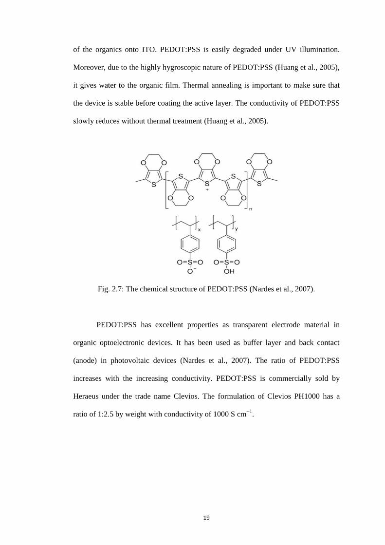
Fig. 2.7: The chemical structure of PEDOT:PSS (Nardes et al., 2007).
PEDOT:PSS has excellent properties as transparent electrode material in
organic optoelectronic devices. It has been used as buffer layer and back contact
(anode) in photovoltaic devices (Nardes et al., 2007). The ratio of PEDOT:PSS
increases with the increasing conductivity. PEDOT:PSS is commercially sold by
Heraeus under the trade name Clevios. The formulation of Clevios PH1000 has a
ratio of 1:2.5 by weight with conductivity of 1000 S cm−1
.

20
CHAPTER 3
MATERIALS AND METHODOLOGY
3.1 Materials
Table 3.1 represents the materials used for organic and hybrid solar cell
fabrication. The materials are as listed in Table 3.1
Table 3.1: Materials for organic and hybrid solar cell fabrication
No Material
1 3-Hexylthiophene ≥99% (3HT)
2 Anhydrous Iron (III) Chloride (FeCl3)
3 Hydrocloric acid (HCl)
4 Chloroform (CHCl3)
5 Methanol (CH3OH)
6 Zinc nitrate hexahydrate ZnO(NO3)2
7 Zinc acetate dehydrate [Zn(CH3COO)2.2H2O]
8 Sodium hydroxide (NaOH)
9 Hexamethylenetetramine (HMT)
10 [6,6]-Phenyl C61 Butyric Acid Methyl Ester >99% (PCBM)
11 Poly (3,4-ethylenedioxylthiophene) Polystyrene Sulfonate (PEDOT:PSS)
3.2 Instrument and characterization
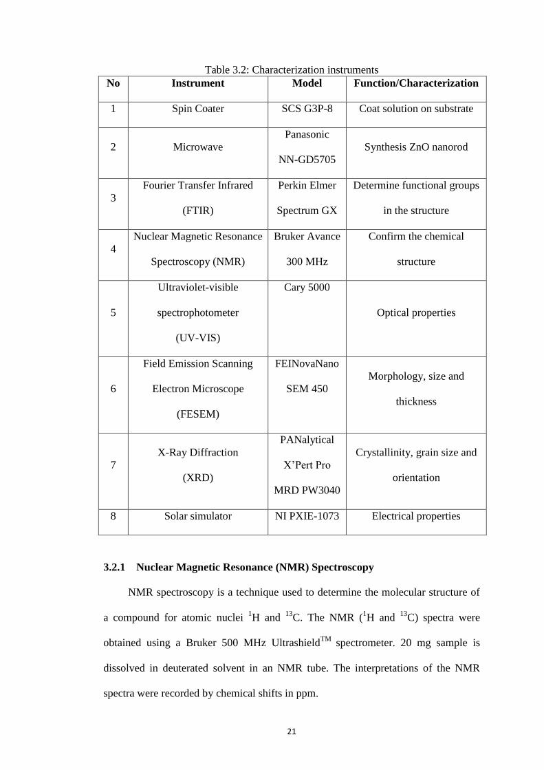
Table 3.2 shows the summary of instruments used for fabrication and
characterization of the materials.
21
Table 3.2: Characterization instruments
No Instrument Model Function/Characterization
1 Spin Coater SCS G3P-8 Coat solution on substrate
2 Microwave
Panasonic
NN-GD5705
Synthesis ZnO nanorod
3
Fourier Transfer Infrared
(FTIR)
Perkin Elmer
Spectrum GX
Determine functional groups
in the structure
4
Nuclear Magnetic Resonance
Spectroscopy (NMR)
Bruker Avance
300 MHz
Confirm the chemical
structure
5
Ultraviolet-visible
spectrophotometer
(UV-VIS)
Cary 5000
Optical properties
6
Field Emission Scanning
Electron Microscope
(FESEM)
FEINovaNano
SEM 450
Morphology, size and
thickness
7
X-Ray Diffraction
(XRD)
PANalytical
X’Pert Pro
MRD PW3040
Crystallinity, grain size and
orientation
8 Solar simulator NI PXIE-1073 Electrical properties
3.2.1 Nuclear Magnetic Resonance (NMR) Spectroscopy
NMR spectroscopy is a technique used to determine the molecular structure of
a compound for atomic nuclei 1H and
13C. The NMR (
1H and
13C) spectra were
obtained using a Bruker 500 MHz UltrashieldTM
spectrometer. 20 mg sample is
dissolved in deuterated solvent in an NMR tube. The interpretations of the NMR
spectra were recorded by chemical shifts in ppm.

22
Fig. 3.1: 300 MHz and 500 MHz NMR instruments.
3.2.2 Fourier Transfer Infrared (FTIR)
FT-IR (Fig. 3.2) is a technique used to determine the functional groups in a
sample. The absorption band is the characteristic of the chemical bond as can be seen
in the spectra. Samples are scanned at range of 700 to 4000 cm-1
. All spectra were
obtained using Perkin Elmer 2000 FTIR.
Fig. 3.2: FT-IR instrument.

23
3.2.3 Ultraviolet-visible (UV-VIS) spectrophotometer
UV-VIS spectrophotometer (Fig. 3.3) is used to analyze materials in the
ultraviolet-visible region. Infrared spectroscopy depends on vibration motions, but
UV-VIS spectroscopy is based on electronic transitions. From UV-VIS spectroscopy,
wavelength and absorbance of material can be determined. To determine absorbance
of material Beer’s Law is being used:
(3.1)
Where A is absorbance, ε is molar extinction coefficient, b is path length and c is
concentration. Energy band gap of a material can be determined by using equation:
(3.2)
Where E is energy, is Planack’s constant, c is speed of light and λ is wavelength.
Fig. 3.3: UV-Vis spectrophotometer.

24
3.2.4 Field Emission Scanning Electron Microscope (FESEM)
FESEM (Fig. 3.4) is a microscope that works with electron, liberated by field
emission source (particle with negative charge) instead of light. FESEM is used to
analyze the morphology, size and thickness of devices.
Fig. 3.4: FESEM microscope.
3.2.5 X-Ray Diffraction (XRD)
XRD (Fig. 3.5) is used to analyze crystalline materials to give data of
crystalline phase, degree of crystallinity, amount of amorphous content and
orientation of crystallites. XRD instrument is using Bragg’s diffraction principle
which is defined by:
(3.3)
Where is an integer, λ is wavelength, d is the inter-planar spacing in the crystal
lattice, θ is the angle between the sample surface and incident beam and ∆ represent
the path difference.
Related Documents