F-Tile Avalon ® Streaming Intel ® FPGA IP for PCI Express* User Guide Updated for Intel ® Quartus ® Prime Design Suite: 22.1 IP Version: 5.0.0 Online Version Send Feedback UG-20331 ID: 683140 Version: 2022.04.04

Welcome message from author
This document is posted to help you gain knowledge. Please leave a comment to let me know what you think about it! Share it to your friends and learn new things together.
Transcript
F-Tile Avalon® Streaming Intel®FPGA IP for PCI Express* User Guide
Updated for Intel® Quartus® Prime Design Suite: 22.1
IP Version: 5.0.0
Online Version
Send Feedback UG-20331
ID: 683140
Version: 2022.04.04
Contents
1. Acronyms........................................................................................................................6
2. Introduction................................................................................................................... 72.1. Overview..............................................................................................................72.2. Features...............................................................................................................72.3. Release Information...............................................................................................92.4. Device Family Support..........................................................................................102.5. Resource Utilization..............................................................................................102.6. IP Core and Design Example Support Levels............................................................ 11
3. IP Architecture and Functional Description...................................................................133.1. Architecture........................................................................................................ 13
3.1.1. Clocks.................................................................................................... 153.1.2. Refclk.....................................................................................................163.1.3. Reset..................................................................................................... 19
3.2. Functional Description.......................................................................................... 213.2.1. PMA/PCS................................................................................................ 213.2.2. Data Link Layer....................................................................................... 223.2.3. Transaction Layer.....................................................................................24
3.3. Avalon-ST TX/RX................................................................................................. 253.3.1. TLP Header and Data Alignment.................................................................263.3.2. Avalon-ST RX.......................................................................................... 263.3.3. Avalon-ST TX.......................................................................................... 303.3.4. Tag Allocation..........................................................................................333.3.5. Completion Buffer Size............................................................................. 34
3.4. Interrupts...........................................................................................................343.4.1. Legacy Interrupts.................................................................................... 343.4.2. MSI........................................................................................................353.4.3. MSI-X.....................................................................................................38
3.5. Completion Timeout............................................................................................. 413.6. Hot Plug............................................................................................................. 433.7. Power Management..............................................................................................433.8. Configuration Output Interface (COI) .....................................................................453.9. Configuration Intercept Interface (EP Only)............................................................. 483.10. Hard IP Reconfiguration Interface.........................................................................50
3.10.1. Configuration Registers Access.................................................................523.11. PHY Reconfiguration Interface..............................................................................553.12. Page Request Service (PRS) (EP Only).................................................................. 56
4. Advanced Features....................................................................................................... 574.1. Virtualization Support...........................................................................................57
4.1.1. Single Root I/O Virtualization (SR-IOV)....................................................... 574.1.2. VirtIO.....................................................................................................62
4.2. TLP Bypass Mode................................................................................................. 704.2.1. Register Settings for TLP Bypass mode....................................................... 714.2.2. Avalon-MM usage for TLP Bypass Mode....................................................... 734.2.3. Transmit Interface....................................................................................744.2.4. Receive Interface..................................................................................... 74
Contents
F-Tile Avalon® Streaming Intel® FPGA IP for PCI Express* User Guide Send Feedback
2
4.2.5. Configuration TLP.....................................................................................744.2.6. Malformed TLP.........................................................................................754.2.7. ECRC..................................................................................................... 75
4.3. Precision Time Measurement (PTM)........................................................................ 754.4. Scalable IOV....................................................................................................... 78
5. Interfaces..................................................................................................................... 795.1. Overview............................................................................................................ 795.2. Clocks and Resets................................................................................................825.3. Serial Data Interface............................................................................................ 845.4. Avalon-ST Interface............................................................................................. 84
5.4.1. Avalon-ST RX Interface Signals..................................................................845.4.2. Avalon-ST TX Interface Signals.................................................................. 90
5.5. Interrupt Interface...............................................................................................955.5.1. Legacy Interrupt Interface Signals..............................................................965.5.2. MSI Pending Bits Interface Signals............................................................. 96
5.6. Hard IP Status Interface....................................................................................... 975.7. Error Interface.....................................................................................................985.8. 10-bit Tag Support Interface................................................................................1025.9. Completion Timeout Interface..............................................................................1025.10. Power Management Interface.............................................................................1035.11. Hot Plug Interface (RP Only).............................................................................. 1065.12. Configuration Output Interface...........................................................................1075.13. Configuration Intercept Interface (EP Only)..........................................................1085.14. Hard IP Reconfiguration Interface....................................................................... 1105.15. PHY Reconfiguration Interface............................................................................ 1115.16. Page Request Service (PRS) Interface (EP Only)................................................... 1115.17. FLR Interface Signals........................................................................................ 1125.18. PTM Interface Signals....................................................................................... 1145.19. VF Error Flag Interface Signals........................................................................... 1155.20. VirtIO PCI Configuration Access Interface Signals................................................. 116
6. Parameters................................................................................................................. 1206.1. Top-Level Settings..............................................................................................1206.2. Core Parameters................................................................................................ 122
6.2.1. Avalon Parameters................................................................................. 1256.2.2. Base Address Registers........................................................................... 1266.2.3. PCI Express and PCI Capabilities Parameters..............................................1276.2.4. Device Identification Registers................................................................. 1406.2.5. Configuration, Debug and Extension Options..............................................142
7. Testbench................................................................................................................... 1447.1. Generating Tile Files........................................................................................... 1457.2. Endpoint Testbench............................................................................................ 1457.3. Test Driver Module............................................................................................. 1467.4. Root Port BFM....................................................................................................147
7.4.1. BFM Memory Map...................................................................................1497.4.2. Configuration Space Bus and Device Numbering......................................... 1497.4.3. Configuration of Root Port and Endpoint.................................................... 1497.4.4. Issuing Read and Write Transactions to the Application Layer....................... 155
7.5. BFM Procedures and Functions.............................................................................1557.5.1. ebfm_barwr Procedure............................................................................155
Contents
Send Feedback F-Tile Avalon® Streaming Intel® FPGA IP for PCI Express* User Guide
3
7.5.2. ebfm_barwr_imm Procedure....................................................................1567.5.3. ebfm_barrd_wait Procedure.....................................................................1567.5.4. ebfm_barrd_nowt Procedure....................................................................1577.5.5. ebfm_cfgwr_imm_wait Procedure.............................................................1577.5.6. ebfm_cfgwr_imm_nowt Procedure............................................................1587.5.7. ebfm_cfgrd_wait Procedure..................................................................... 1587.5.8. ebfm_cfgrd_nowt Procedure.................................................................... 1597.5.9. BFM Configuration Procedures..................................................................1597.5.10. BFM Shared Memory Access Procedures.................................................. 1617.5.11. BFM Log and Message Procedures...........................................................1637.5.12. Verilog HDL Formatting Functions........................................................... 166
8. Troubleshooting/Debugging....................................................................................... 1708.1. Hardware..........................................................................................................170
8.1.1. Debugging Link Training Issues................................................................ 1718.1.2. Debugging Data Transfer and Performance Issues.......................................178
8.2. Debug Toolkit.................................................................................................... 1828.2.1. Overview.............................................................................................. 1828.2.2. Enabling the F-Tile Debug Toolkit..............................................................1848.2.3. Launching the F-Tile Debug Toolkit............................................................1848.2.4. Using the F-Tile Debug Toolkit..................................................................1878.2.5. Using the F-Tile Link Inspector................................................................. 198
9. F-Tile Avalon Streaming Intel FPGA IP for PCI Express User Guide Archives.............. 201
10. Revision History of the F-Tile Avalon Streaming Intel FPGA IP for PCI ExpressUser Guide.............................................................................................................202
A. Configuration Space Registers.................................................................................... 203A.1. Configuration Space Registers..............................................................................203
A.1.1. Register Access Definitions...................................................................... 205A.1.2. PCIe Configuration Header Registers.........................................................205A.1.3. PCI Express Capability Structures.............................................................207A.1.4. Physical Layer 16.0 GT/s Extended Capability Structure...............................208A.1.5. MSI-X Registers..................................................................................... 209
A.2. Configuration Space Registers for Virtualization......................................................210A.2.1. SR-IOV Virtualization Extended Capabilities Registers Address Map............... 210A.2.2. PCIe Configuration Registers for Each Virtual Function.................................211
A.3. Intel-Defined VSEC Capability Registers................................................................ 216A.3.1. Intel-Defined VSEC Capability Header (Offset 00h)..................................... 216A.3.2. Intel-Defined Vendor Specific Header (Offset 04h)...................................... 217A.3.3. Intel Marker (Offset 08h)........................................................................ 217A.3.4. JTAG Silicon ID (Offset 0x0C - 0x18)........................................................ 217A.3.5. User Configurable Device and Board ID (Offset 0x1C - 0x1D).......................218A.3.6. General Purpose Control and Status Register (Offset 0x30)..........................218A.3.7. Uncorrectable Internal Error Status Register (Offset 0x34)...........................218A.3.8. Uncorrectable Internal Error Mask Register (Offset 0x38)............................ 219A.3.9. Correctable Internal Error Status Register (Offset 0x3C)..............................220A.3.10. Correctable Internal Error Mask Register (Offset 0x40)..............................220
B. Implementation of Address Translation Services (ATS) in Endpoint Mode.................. 222B.1. Sending Translated/Untranslated Requests............................................................ 222
Contents
F-Tile Avalon® Streaming Intel® FPGA IP for PCI Express* User Guide Send Feedback
4
B.2. Sending a Page Request Message from the Endpoint (EP) to the Root Complex (RC)... 222B.3. Invalidating Requests/Completions....................................................................... 222
C. Packets Forwarded to the User Application in TLP Bypass Mode................................. 223C.1. EP TLP Bypass Mode (Upstream)..........................................................................223C.2. RC TLP Bypass Mode (Downstream)..................................................................... 228
D. Root Port Enumeration............................................................................................... 234
E. Bifurcated Endpoint Support for Independent Resets................................................. 240E.1. PCI Express Resets.............................................................................................240E.2. Supported Configurations....................................................................................241
E.2.1. Configuration Type A.............................................................................. 241E.2.2. Configuration Type B.............................................................................. 244E.2.3. Configuration Type C.............................................................................. 245
Contents
Send Feedback F-Tile Avalon® Streaming Intel® FPGA IP for PCI Express* User Guide
5
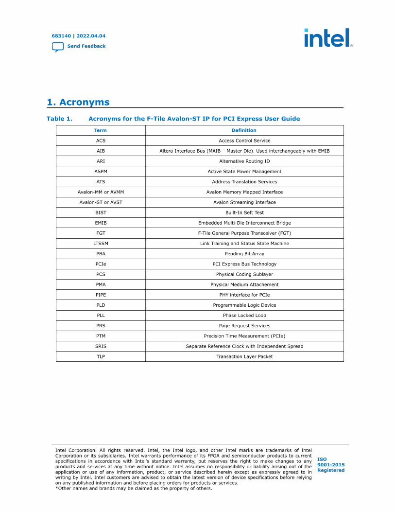
1. AcronymsTable 1. Acronyms for the F-Tile Avalon-ST IP for PCI Express User Guide
Term Definition
ACS Access Control Service
AIB Altera Interface Bus (MAIB – Master Die). Used interchangeably with EMIB
ARI Alternative Routing ID
ASPM Active State Power Management
ATS Address Translation Services
Avalon-MM or AVMM Avalon Memory Mapped Interface
Avalon-ST or AVST Avalon Streaming Interface
BIST Built-In Seft Test
EMIB Embedded Multi-Die Interconnect Bridge
FGT F-Tile General Purpose Transceiver (FGT)
LTSSM Link Training and Status State Machine
PBA Pending Bit Array
PCIe PCI Express Bus Technology
PCS Physical Coding Sublayer
PMA Physical Medium Attachement
PIPE PHY interface for PCIe
PLD Programmable Logic Device
PLL Phase Locked Loop
PRS Page Request Services
PTM Precision Time Measurement (PCIe)
SRIS Separate Reference Clock with Independent Spread
TLP Transaction Layer Packet
683140 | 2022.04.04
Send Feedback
Intel Corporation. All rights reserved. Intel, the Intel logo, and other Intel marks are trademarks of IntelCorporation or its subsidiaries. Intel warrants performance of its FPGA and semiconductor products to currentspecifications in accordance with Intel's standard warranty, but reserves the right to make changes to anyproducts and services at any time without notice. Intel assumes no responsibility or liability arising out of theapplication or use of any information, product, or service described herein except as expressly agreed to inwriting by Intel. Intel customers are advised to obtain the latest version of device specifications before relyingon any published information and before placing orders for products or services.*Other names and brands may be claimed as the property of others.
ISO9001:2015Registered
2. Introduction
2.1. Overview
The F-Tile Intel® Quartus® Prime Hard IP supports PCI Express* Gen4 in Endpoint,Root Port and TLP Bypass Modes. The F-Tile Intel Quartus Prime Hard IP supportsAvalon Streaming user interfaces. F-tile serves as a companion tile for Intel Agilex™
devices.
F-Tile is the successor of P-Tile and natively supports PCI Express Gen3 and Gen4configurations.
2.2. Features
The F-Tile Avalon® Streaming Interface for PCI Express supports the followingfeatures:
PCIe* Features
• Complete protocol stack including the Transaction, Data Link and Physical Layersimplemented as a Hard IP.
• Topologies supported:
Table 2. Topologies Supported
Gen3/Gen4 x16 Gen3/Gen4 x8 Gen3/Gen4 x4
Endpoint Yes Yes Yes
Root Port Yes Yes Yes
TLP-Bypass Yes Yes Yes
Note: Gen1/Gen2 or lower link width configurations are supported via link down-training
• Supports up to 512-byte maximum payload size (MPS).
• Supports Single Virtual Channel (VC).
• Supports Completion Timeout Ranges through Completion Timeout Interface
• Atomic Operations (FetchAdd/Swap/CAS).
• Extended Tag Support. (10-bit Tag Support Applies to x16 ports only. Maximum512 Outstanding Non-Posted Request)
• Separate Refclk with Independent Spread Spectrum Clocking (SRIS).
• Separate Refclk with no Spread Spectrum Clocking (SRNS).
• Common Refclk architecture.
683140 | 2022.04.04
Send Feedback
Intel Corporation. All rights reserved. Intel, the Intel logo, and other Intel marks are trademarks of IntelCorporation or its subsidiaries. Intel warrants performance of its FPGA and semiconductor products to currentspecifications in accordance with Intel's standard warranty, but reserves the right to make changes to anyproducts and services at any time without notice. Intel assumes no responsibility or liability arising out of theapplication or use of any information, product, or service described herein except as expressly agreed to inwriting by Intel. Intel customers are advised to obtain the latest version of device specifications before relyingon any published information and before placing orders for products or services.*Other names and brands may be claimed as the property of others.
ISO9001:2015Registered
• PCI Express Advanced Error Reporting (Physical Function only).
• ECRC generation and checking.
• Data bus parity protection.
• Supports D0 and D3 PCIe power states.
• Lane Margining at Receiver.
• Retimers presence detection.
Multifunction and Virtualization Features:
• Single Root-IO Virtualization (SRIOV). Up to 2048 Virtual Functions.
• ACS Control Service (ACS) capability support for Port 0 and 1 (x16 Core and x8Core)
• Alternative Routing-ID Interpretation (ARI).
• Function Level Reset (FLR).
• TLP Processing Hint (TPH).
Note: TPH supports the "No Steering Tag (ST)" mode only.
• Address Translation Services (ATS)
• Supports Page Request Services (PRS).
• Process Address Space ID (PASID).
• Configuration Intercept Interface (for VirtIO).
Avalon Streaming Interface IP Features:
• User packet interface with separate header, data and prefix.
• User packet interface with a split-bus architecture where the header, data andprefix busses consist of two segments each (x16 mode only). This improves thebandwidth efficiency of this interface as it can handle up to 2 TLPs in any givencycle.
• Up to 512 outstanding Non-Posted request for Port 0 (x16 core)
• Up to 256 outstanding Non-Posted request for Port 1,2 and 3 (x8 and x4 cores)
• Supports Autonomous Hard IP mode. This mode allows the PCIe Hard IP tocommunicate with the Host before the FPGA configuration and entry into usermode are complete.
Note: Unless Readiness Notifications mechanisms are used, the Root Complexand/or system software must allow at least one second after a ConventionalReset of a device before it may determine that a device that fails to return aSuccessful Completion status for a valid Configuration Request is a brokendevice. This period is independent of how quickly Link training is complete.
• FPGA core configuration via PCIe link (CvP Init and CvP Update) supported by thex16Core or Port 0 only
• Variable PLD clock frequencies: (350 MHz / 400 MHz / 450 MHz / 500 MHz forIntel Agilex)
• Legacy Interrupts
• MSI/MSI-X interrupts
2. Introduction
683140 | 2022.04.04
F-Tile Avalon® Streaming Intel® FPGA IP for PCI Express* User Guide Send Feedback
8
• Configuration Extension Bus & VSEC via CII interface
Note: CII Interface is not supported for 1 x4 configuration or Topology H.
• Precision Time Measurement (PTM) (PTM Requester only)
Note: You can enable PTM only in one core (either x16 or x8) at any given time.
• Parity Support on Avalon-ST interface
• The FPGA pin allocations for the F-Tile Avalon Streaming IP for PCI Express in theIntel Quartus Prime project is fixed. However, this IP does support lane reversaland polarity inversion on the PCB by default.
• Modelsim and VCS are the simulators supported in the Intel Quartus Prime 21.3release. Other simulators may be supported in a future release.
Standards and Specification Compliance
• PCI Express Base Specification Revision 4.0
• Single Root I/O Virtualization and Sharing Specification, Rev 1.1
• Address Translation Services, Revision 1.1
• PHY Interface for PCI Express Architectures, Version 4.x (the spec thatcorresponds to PCI Express Base Spec, Revision 4.0)
• Virtual I/O Device (VIRTIO) Version 1.0
Note: Throughout this User Guide, the term AVST or Avalon-ST may be used as anabbreviation for the Avalon Streaming Interface IP.
2.3. Release Information
Table 3. F-Tile Avalon streaming IP for PCI Express Release Information
Item Description
IP Version 5.0.0
Intel Quartus Prime Version 22.1
Release Date March 2022
Ordering Codes No ordering code is required
IP versions are the same as the Intel Quartus Prime Design Suite software versions upto v19.1. From Intel Quartus Prime Design Suite software version 19.2 or later, IPshave a new IP versioning scheme.
The IP version (X.Y.Z) number may change from one Intel Quartus Prime softwareversion to another. A change in:
• X indicates a major revision of the IP. If you update your Intel Quartus Primesoftware, you must regenerate the IP.
• Y indicates the IP includes new features. Regenerate your IP to include these newfeatures.
• Z indicates the IP includes minor changes. Regenerate your IP to include thesechanges.
2. Introduction
683140 | 2022.04.04
Send Feedback F-Tile Avalon® Streaming Intel® FPGA IP for PCI Express* User Guide
9
Intel verifies that the current version of the Intel Quartus Prime Pro Edition softwarecompiles the previous version of each IP core, if this IP core was included in theprevious release. Intel reports any exceptions to this verification in the Intel IPRelease Notes or clarifies them in the Intel Quartus Prime Pro Edition IP Update tool.Intel does not verify compilation with IP core versions older than the previous release.
2.4. Device Family Support
The following terms define device support levels for Intel FPGA IP cores:
• Advance support: the IP core is available for simulation and compilation for thisdevice family. Timing models include initial engineering estimates of delays basedon early post-layout information. The timing models are subject to change assilicon testing improves the correlation between the actual silicon and the timingmodels. You can use this IP core for system architecture and resource utilizationstudies, simulation, pinout, system latency assessments, basic timing assessments(pipeline budgeting), and I/O transfer strategy (data-path width, burst depth, I/Ostandards tradeoffs).
• Preliminary support: the IP core is verified with preliminary timing models for thisdevice family. The IP core meets all functional requirements, but might still beundergoing timing analysis for the device family. It can be used in productiondesigns with caution.
• Final support: the IP core is verified with final timing models for this device family.The IP core meets all functional and timing requirements for the device family andcan be used in production designs.
Table 4. Device Family Support
Device Family Support Level
Intel Agilex Preliminary support
Other device families No supportRefer to the Intel PCI Express Solutions web page on theIntel website for support information on
2.5. Resource Utilization
The following table shows the recommended FPGA fabric speed grades for all theconfigurations that the Avalon-ST IP core supports.
Table 5. Intel Agilex Recommended FPGA Fabric Speed Grades for All Avalon-STWidths and FrequenciesThe recommended FPGA fabric speed grades are for production parts.
Lane Rate Link Width Application InterfaceData Width
Application ClockFrequency (MHz)
Recommended FPGAFabric Speed Grades
Gen4 x16 512-bit 500 MHz / 400 MHz /350 MHz
-1,-2
450 MHz -3
x8 256-bit 500 MHz / 400 MHz /350 MHz
-1,-2
450 MHz -3
continued...
2. Introduction
683140 | 2022.04.04
F-Tile Avalon® Streaming Intel® FPGA IP for PCI Express* User Guide Send Feedback
10
Lane Rate Link Width Application InterfaceData Width
Application ClockFrequency (MHz)
Recommended FPGAFabric Speed Grades
x4 128-bit 500 MHz / 400 MHz /350 MHz
-1,-2
450 MHz -3
Gen3 x16 512-bit 250 MHz -2, -3
x8 256-bit 250 MHz -2, -3
x4 128-bit 250 MHz -2, -3
Note: Speed Grade -3 may be supported in a future release.
The following table shows the typical resource utilization information for selectedconfigurations.
The resource usage is based on the Avalon-ST IP core top-level entity(intel_pcie_ftile_ast) that includes IP core soft logic implemented in the FPGAfabric.
Table 6. Resource Utilization Information of the IP
IP Configuration Device Family ALMs M20Ks Logic Registers
Gen4 x16, EP Intel Agilex 7461 11 14,845
Gen4 x16, RP Intel Agilex 7462 11 15,032
Gen4 x8x8, EP Intel Agilex 7605 11 15,331
Gen4 x8, EP Intel Agilex 5844 11 10,822
Gen4 x8, RP Intel Agilex 5857 11 10,898
Gen4 x4, EP Intel Agilex 5327 11 9,499
Gen4 x4x4, RP Intel Agilex 6717 11 12,668
Gen4 x4x4x4x4, RP Intel Agilex 9326 11 18,823
Note: The default IP parameter is used for each of the IP configurations above, resourceutilization may increase as additional IP features enabled. The resource utilization ofthe IP above has taken the tile logic into account.
2.6. IP Core and Design Example Support Levels
The following table shows the support levels of the Avalon-ST IP core and designexample in Intel Agilex devices.
2. Introduction
683140 | 2022.04.04
Send Feedback F-Tile Avalon® Streaming Intel® FPGA IP for PCI Express* User Guide
11
Table 7. F-Tile Avalon Streaming (Avalon-ST) IP for PCIe Support Matrix for IntelAgilex DevicesSupport level keys: S = simulation, C = compilation, T = timing, H = hardware, N/A = configuration notsupported
ConfigurationPCIe IP Support Design Example Support
End Point Root Port TLP-Bypass End Point Root Port TLP Bypass
Gen4 x16 512-bit
S, C, T, H S, C, T, H S, C, T, H S,C,T N/A N/A
Gen4 x8/x8256-bit
S, C, T, H N/A S, C, T, H S,C,T N/A N/A
Gen4 x8 256-bit
S, C, T, H S, C, T, H N/A S,C,T N/A N/A
Gen4x4/x4/x4/x4128-bit
N/A S, C, T, H S, C, T, H N/A N/A N/A
Gen4 x4/x4128-bit
N/A S, C, T, H N/A N/A N/A N/A
Gen4 x4 128-bit
S, C, T, H N/A N/A N/A N/A N/A
Gen3 x16 512-bit
S, C, T, H S, C, T, H S, C, T, H S,C,T N/A N/A
Gen3 x8/x8256-bit
S, C, T, H N/A S, C, T, H S,C,T N/A N/A
Gen3 x8 256-bit
S, C, T, H S, C, T, H N/A S,C,T N/A N/A
Gen3x4/x4/x4/x4128-bit
N/A S, C, T, H S, C, T, H N/A N/A N/A
Gen3 x4/x4128-bit
N/A S, C, T, H N/A N/A N/A N/A
Gen3 x4 128-bit
S, C, T, H N/A N/A N/A N/A N/A
2. Introduction
683140 | 2022.04.04
F-Tile Avalon® Streaming Intel® FPGA IP for PCI Express* User Guide Send Feedback
12
3. IP Architecture and Functional Description
3.1. Architecture
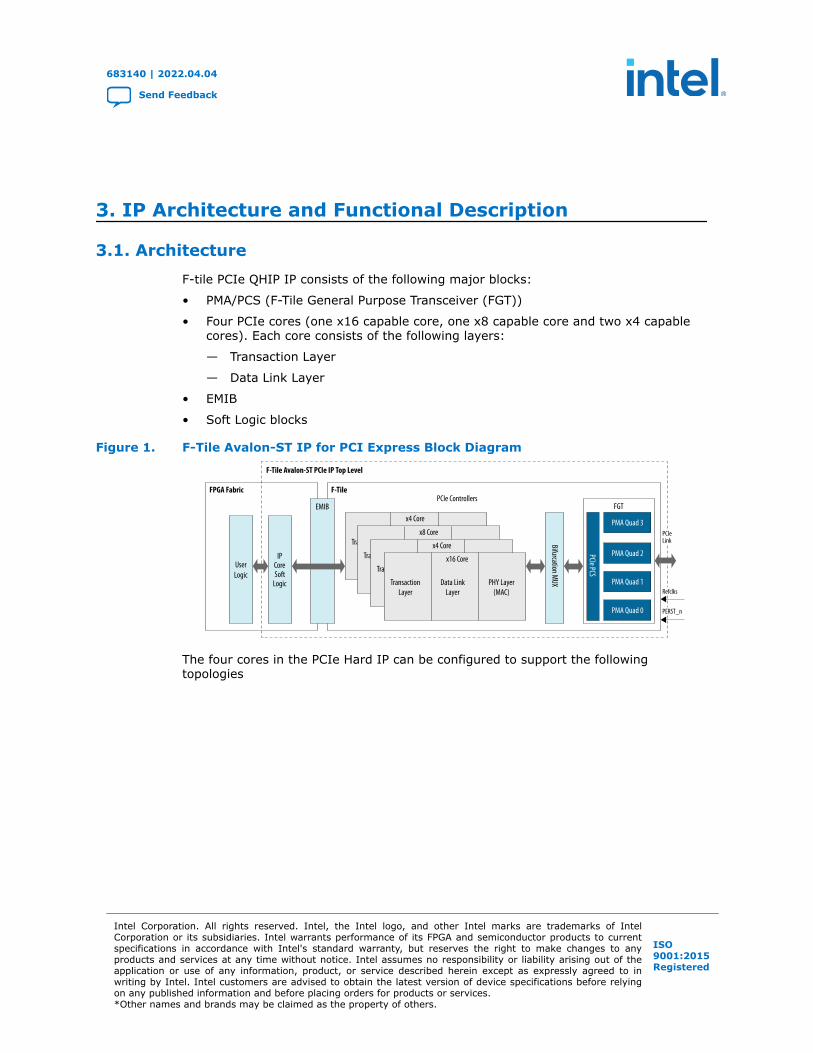
F-tile PCIe QHIP IP consists of the following major blocks:
• PMA/PCS (F-Tile General Purpose Transceiver (FGT))
• Four PCIe cores (one x16 capable core, one x8 capable core and two x4 capablecores). Each core consists of the following layers:
— Transaction Layer
— Data Link Layer
• EMIB
• Soft Logic blocks
Figure 1. F-Tile Avalon-ST IP for PCI Express Block Diagram
PCIe Controllers
UserLogic
IPCoreSoft
Logic
F-TileFPGA Fabric
F-Tile Avalon-ST PCIe IP Top Level
TransactionLayer
Data LinkLayer
PHY Layer(MAC)
x4 Core
x8 Core
TransactionLayer
Data LinkLayer
PHY Layer(MAC)
x4 Core
TransactionLayer
Data LinkLayer
PHY Layer(MAC)
x16 Core
TransactionLayer
Data LinkLayer
PHY Layer(MAC)
EMIB FGT
PMA Quad 3
PMA Quad 2
PMA Quad 1
PCIe PCS
Bifurcation MUX
PMA Quad 0
PCIeLink
Refclks
PERST_n
The four cores in the PCIe Hard IP can be configured to support the followingtopologies
683140 | 2022.04.04
Send Feedback
Intel Corporation. All rights reserved. Intel, the Intel logo, and other Intel marks are trademarks of IntelCorporation or its subsidiaries. Intel warrants performance of its FPGA and semiconductor products to currentspecifications in accordance with Intel's standard warranty, but reserves the right to make changes to anyproducts and services at any time without notice. Intel assumes no responsibility or liability arising out of theapplication or use of any information, product, or service described herein except as expressly agreed to inwriting by Intel. Intel customers are advised to obtain the latest version of device specifications before relyingon any published information and before placing orders for products or services.*Other names and brands may be claimed as the property of others.
ISO9001:2015Registered
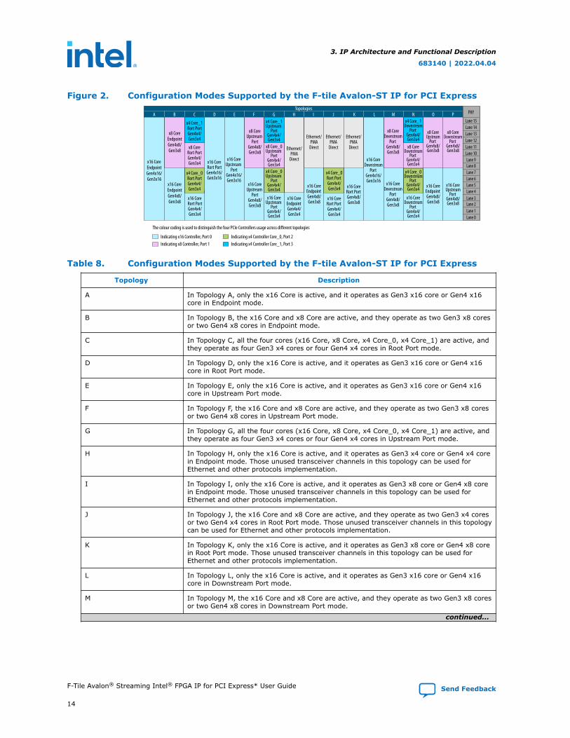
Figure 2. Configuration Modes Supported by the F-tile Avalon-ST IP for PCI ExpressTopologies
A B C D E F G H I J K L M N O P
x8 CoreEndpointGen4x8/Gen3x8
x4 Core_1Upstream
PortGen4x4/Gen3x4
Ethernet/PMA
Direct
Ethernet/PMA
Direct
Ethernet/PMA
Direct
Ethernet/PMA
Direct
x4 Core_0Downstream
Port Gen4x4/Gen3x4
x4 Core_1Downstream
Port Gen4x4/Gen3x4
x4 Core_0Rort Port Gen4x4/Gen3x4
x4 Core_0Rort PortGen4x4/Gen3x4
x4 Core_1Rort PortGen4x4/Gen3x4
x16 CoreEndpointGen4x16/Gen3x16
x16 CoreEndpointGen4x8/Gen3x8
x16 CoreRort PortGen4x4/Gen3x4
x16 CoreUpstream
PortGen4x4/Gen3x4
x16 CoreEndpoint Gen4x4/Gen3x4
x16 CoreRort Port Gen4x4/Gen3x4
x16 CoreRort Port Gen4x8/Gen3x8
x16 CoreDownstream
Port Gen4x16/Gen3x16 x16 Core
DownstreamPort
Gen4x8/Gen3x8
x16 CoreDownstream
Port Gen4x4/Gen3x4
x16 CoreUpstream
Port Gen4x8/Gen3x8
x16 CoreEndpoint Gen4x8/Gen3x8
x16 CoreEndpoint Gen4x8/Gen3x8
x16 CoreRort PortGen4x16/Gen3x16
x16 CoreUpstream
PortGen4x16/Gen3x16
x16 CoreUpstream
PortGen4x8/Gen3x8
x8 Core_0Upstream
PortGen4x4/Gen3x4
x8 CoreDownstream
Port Gen4x8/Gen3x8
x8 CoreDownstream
Port Gen4x4/Gen3x4
x8 CoreDownstream
Port Gen4x8/Gen3x8
x8 CoreUpstream
Port Gen4x8/Gen3x8
x8 CoreRort PortGen4x4/Gen3x4
x8 CoreUpstream
PortGen4x8/Gen3x8
x4 Core_0Upstream
PortGen4x4/Gen3x4
PHY
Lane 15Lane 14Lane 13Lane 12Lane 11Lane 10Lane 9Lane 8Lane 7Lane 6Lane 5Lane 4Lane 3Lane 2Lane 1Lane 0
The colour coding is used to distinguish the four PCIe Controllers usage across different topologies
Indicating x16 Controller, Port 0Indicating x8 Controller, Port 1
Indicating x4 Controller Core_0, Port 2Indicating x4 Controller Core_1, Port 3
Table 8. Configuration Modes Supported by the F-tile Avalon-ST IP for PCI Express
Topology Description
A In Topology A, only the x16 Core is active, and it operates as Gen3 x16 core or Gen4 x16core in Endpoint mode.
B In Topology B, the x16 Core and x8 Core are active, and they operate as two Gen3 x8 coresor two Gen4 x8 cores in Endpoint mode.
C In Topology C, all the four cores (x16 Core, x8 Core, x4 Core_0, x4 Core_1) are active, andthey operate as four Gen3 x4 cores or four Gen4 x4 cores in Root Port mode.
D In Topology D, only the x16 Core is active, and it operates as Gen3 x16 core or Gen4 x16core in Root Port mode.
E In Topology E, only the x16 Core is active, and it operates as Gen3 x16 core or Gen4 x16core in Upstream Port mode.
F In Topology F, the x16 Core and x8 Core are active, and they operate as two Gen3 x8 coresor two Gen4 x8 cores in Upstream Port mode.
G In Topology G, all the four cores (x16 Core, x8 Core, x4 Core_0, x4 Core_1) are active, andthey operate as four Gen3 x4 cores or four Gen4 x4 cores in Upstream Port mode.
H In Topology H, only the x16 Core is active, and it operates as Gen3 x4 core or Gen4 x4 corein Endpoint mode. Those unused transceiver channels in this topology can be used forEthernet and other protocols implementation.
I In Topology I, only the x16 Core is active, and it operates as Gen3 x8 core or Gen4 x8 corein Endpoint mode. Those unused transceiver channels in this topology can be used forEthernet and other protocols implementation.
J In Topology J, the x16 Core and x8 Core are active, and they operate as two Gen3 x4 coresor two Gen4 x4 cores in Root Port mode. Those unused transceiver channels in this topologycan be used for Ethernet and other protocols implementation.
K In Topology K, only the x16 Core is active, and it operates as Gen3 x8 core or Gen4 x8 corein Root Port mode. Those unused transceiver channels in this topology can be used forEthernet and other protocols implementation.
L In Topology L, only the x16 Core is active, and it operates as Gen3 x16 core or Gen4 x16core in Downstream Port mode.
M In Topology M, the x16 Core and x8 Core are active, and they operate as two Gen3 x8 coresor two Gen4 x8 cores in Downstream Port mode.
continued...
3. IP Architecture and Functional Description
683140 | 2022.04.04
F-Tile Avalon® Streaming Intel® FPGA IP for PCI Express* User Guide Send Feedback
14
Topology Description
N In Topology N, all the four cores (x16 Core, x8 Core, x4 Core_0, x4 Core_1) are active, andthey operate as four Gen3 x4 cores or four Gen4 x4 cores in Downstream Port mode.
O In Topology O, the x16 Core and x8 Core are active, and they operate as two Gen3 x8 coresor two Gen4 x8 cores in Endpoint mode and Upstream Port mode respectively.
P In Topology P, the x16 Core and x8 Core are active, and they operate as two Gen3 x8 coresor two Gen4 x8 cores in Upstream Port mode and Downstream Port mode respectively.
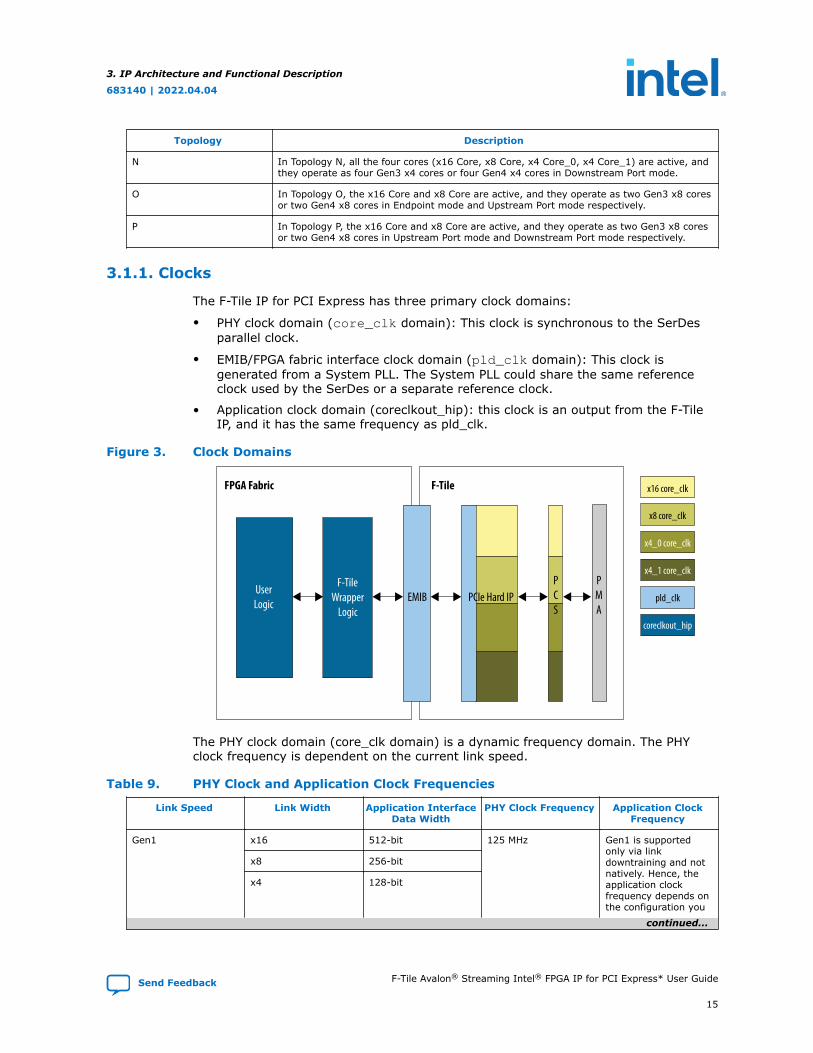
3.1.1. Clocks
The F-Tile IP for PCI Express has three primary clock domains:
• PHY clock domain (core_clk domain): This clock is synchronous to the SerDesparallel clock.
• EMIB/FPGA fabric interface clock domain (pld_clk domain): This clock isgenerated from a System PLL. The System PLL could share the same referenceclock used by the SerDes or a separate reference clock.
• Application clock domain (coreclkout_hip): this clock is an output from the F-TileIP, and it has the same frequency as pld_clk.
Figure 3. Clock Domains
FPGA Fabric F-Tile
UserLogic
F-TileWrapper
Logic
PMA
PCS
PCIe Hard IPEMIB
x16 core_clk
x8 core_clk
x4_0 core_clk
x4_1 core_clk
pld_clk
coreclkout_hip
The PHY clock domain (core_clk domain) is a dynamic frequency domain. The PHYclock frequency is dependent on the current link speed.
Table 9. PHY Clock and Application Clock Frequencies
Link Speed Link Width Application InterfaceData Width
PHY Clock Frequency Application ClockFrequency
Gen1 x16 512-bit 125 MHz Gen1 is supportedonly via linkdowntraining and notnatively. Hence, theapplication clockfrequency depends onthe configuration you
x8 256-bit
x4 128-bit
continued...
3. IP Architecture and Functional Description
683140 | 2022.04.04
Send Feedback F-Tile Avalon® Streaming Intel® FPGA IP for PCI Express* User Guide
15
Link Speed Link Width Application InterfaceData Width
PHY Clock Frequency Application ClockFrequency
select in the IPParameter Editor. Forexample, if you selecta Gen3 configuration,the application clockfrequency is 250 MHz.
Gen2 x16 512-bit 250 MHz Gen2 is supportedonly via linkdowntraining and notnatively. Hence, theapplication clockfrequency depends onthe configuration youselect in the IPParameter Editor. Forexample, if you selecta Gen3 configuration,the application clockfrequency is 250 MHz.
x8 256-bit
x4 128-bit
Gen3 x16 512-bit 500 MHz 250 MHz
x8 256-bit
x4 128-bit
Gen4 x16 512-bit 1000 MHz 350 MHz / 400 MHz /450 MHz / 500 MHzNote: As the data
width remainsunchanged,using lowerfrequencyresults in lowerdatathroughput.
x8 256-bit
x4 128-bit
Note: For a link down-training scenario when the F-Tile is configured at Gen3 or Gen4 andthe link gets down-trained to a lower speed, the application clock frequency continuesto run at the configured frequency set in the PLD Clock Frequency parameter. Forexample, the PCIe Hard IP Mode parameter is set as Gen4 1x16 and the PLD ClockFrequency parameter as 500 MHz, the PLD clock frequency continues to run at 500MHz even if the Link is down trained to Gen 3 or less.
3.1.2. Refclk
There are ten reference clock pins for FGT PMAs at the package level. Eight of the FGTreference clocks (refclk[0]-refclk[7]) can be used as reference clock inputs forPCI Express channels. There are up to four reference clock ports (refclk0 –refclk3) in the F-Tile Avalon Streaming IP for PCI Express depending on the Hard IPmode configuration in the IP. For Hard IP modes that span more than one FGT quads,you must use reference clock pins that are accessible by the quads. Depending on theHIP mode, you must assign the reference clock ports of the IP to correspondingreference clock pins in your Intel Quartus Prime design.
The table below shows the mapping of reference clock pins to the reference clockports of the F-Tile Avalon Streaming IP for PCI Express depending on the Hard IPmode.
3. IP Architecture and Functional Description
683140 | 2022.04.04
F-Tile Avalon® Streaming Intel® FPGA IP for PCI Express* User Guide Send Feedback
16
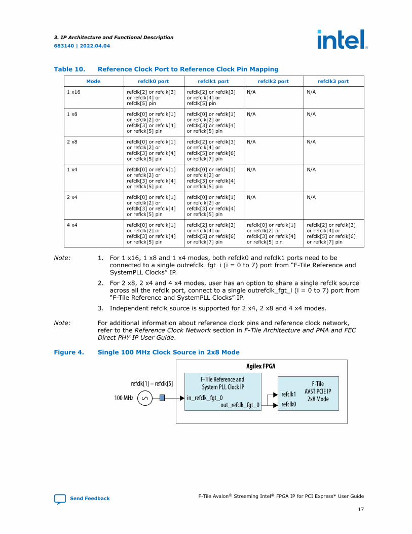
Table 10. Reference Clock Port to Reference Clock Pin Mapping
Mode refclk0 port refclk1 port refclk2 port refclk3 port
1 x16 refclk[2] or refclk[3]or refclk[4] orrefclk[5] pin
refclk[2] or refclk[3]or refclk[4] orrefclk[5] pin
N/A N/A
1 x8 refclk[0] or refclk[1]or refclk[2] orrefclk[3] or refclk[4]or reflck[5] pin
refclk[0] or refclk[1]or refclk[2] orrefclk[3] or refclk[4]or reflck[5] pin
N/A N/A
2 x8 refclk[0] or refclk[1]or refclk[2] orrefclk[3] or refclk[4]or reflck[5] pin
refclk[2] or refclk[3]or refclk[4] orrefclk[5] or refclk[6]or reflck[7] pin
N/A N/A
1 x4 refclk[0] or refclk[1]or refclk[2] orrefclk[3] or refclk[4]or reflck[5] pin
refclk[0] or refclk[1]or refclk[2] orrefclk[3] or refclk[4]or reflck[5] pin
N/A N/A
2 x4 refclk[0] or refclk[1]or refclk[2] orrefclk[3] or refclk[4]or reflck[5] pin
refclk[0] or refclk[1]or refclk[2] orrefclk[3] or refclk[4]or reflck[5] pin
N/A N/A
4 x4 refclk[0] or refclk[1]or refclk[2] orrefclk[3] or refclk[4]or reflck[5] pin
refclk[2] or refclk[3]or refclk[4] orrefclk[5] or refclk[6]or reflck[7] pin
refclk[0] or refclk[1]or refclk[2] orrefclk[3] or refclk[4]or reflck[5] pin
refclk[2] or refclk[3]or refclk[4] orrefclk[5] or refclk[6]or reflck[7] pin
Note: 1. For 1 x16, 1 x8 and 1 x4 modes, both refclk0 and refclk1 ports need to beconnected to a single outrefclk_fgt_i (i = 0 to 7) port from “F-Tile Reference andSystemPLL Clocks” IP.
2. For 2 x8, 2 x4 and 4 x4 modes, user has an option to share a single refclk sourceacross all the refclk port, connect to a single outrefclk_fgt_i (i = 0 to 7) port from“F-Tile Reference and SystemPLL Clocks” IP.
3. Independent refclk source is supported for 2 x4, 2 x8 and 4 x4 modes.
Note: For additional information about reference clock pins and reference clock network,refer to the Reference Clock Network section in F-Tile Architecture and PMA and FECDirect PHY IP User Guide.
Figure 4. Single 100 MHz Clock Source in 2x8 Mode
Agilex FPGA
F-Tile Reference and System PLL Clock IP F-Tile
AVST PCIE IP2x8 Mode
refclk1
refclk[1] – refclk[5]
refclk0in_refclk_fgt_0
out_refclk_fgt_0100 MHz
3. IP Architecture and Functional Description
683140 | 2022.04.04
Send Feedback F-Tile Avalon® Streaming Intel® FPGA IP for PCI Express* User Guide
17
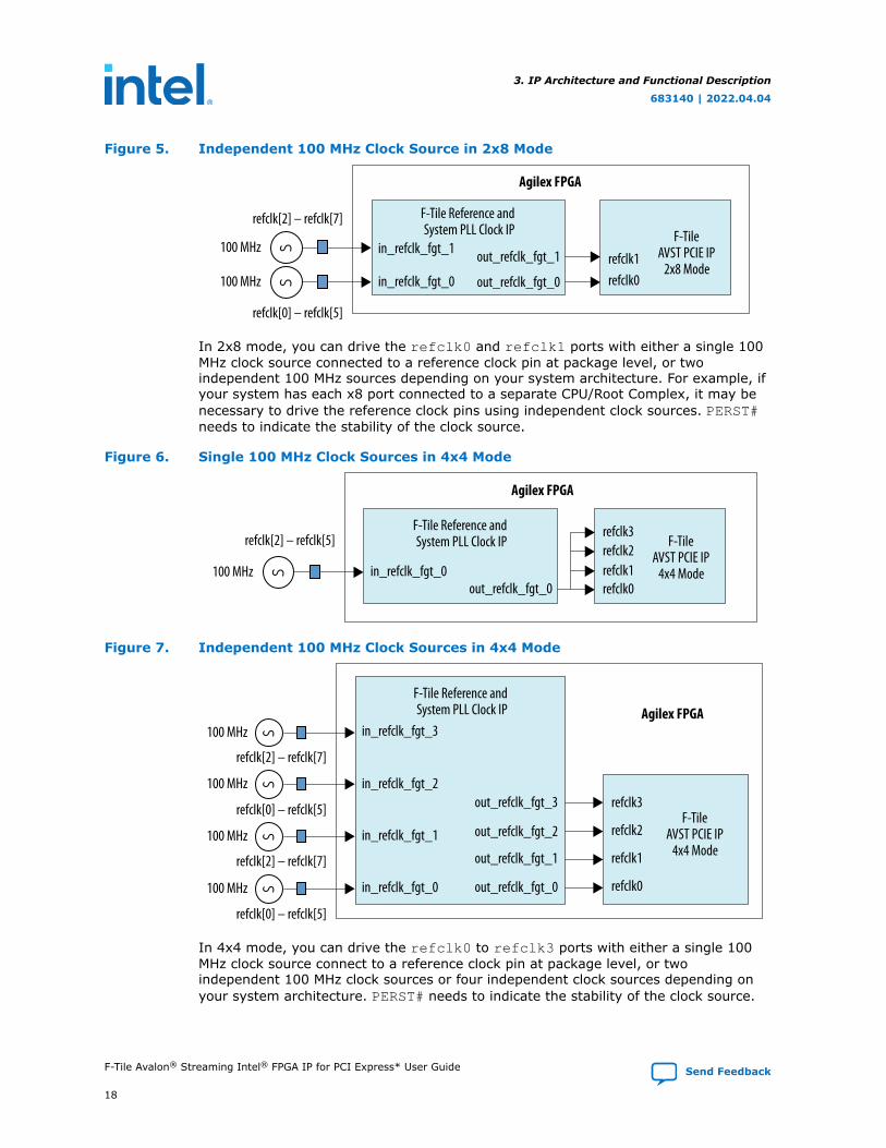
Figure 5. Independent 100 MHz Clock Source in 2x8 Mode
Agilex FPGA
F-Tile Reference and System PLL Clock IP F-Tile
AVST PCIE IP2x8 Mode
refclk1refclk0in_refclk_fgt_0
in_refclk_fgt_1
out_refclk_fgt_0
out_refclk_fgt_1
refclk[2] – refclk[7]
refclk[0] – refclk[5]
100 MHz
100 MHz
In 2x8 mode, you can drive the refclk0 and refclk1 ports with either a single 100MHz clock source connected to a reference clock pin at package level, or twoindependent 100 MHz sources depending on your system architecture. For example, ifyour system has each x8 port connected to a separate CPU/Root Complex, it may benecessary to drive the reference clock pins using independent clock sources. PERST#needs to indicate the stability of the clock source.
Figure 6. Single 100 MHz Clock Sources in 4x4 Mode
Agilex FPGA
F-Tile Reference and System PLL Clock IP F-Tile
AVST PCIE IP4x4 Moderefclk1
refclk2refclk3
refclk0in_refclk_fgt_0
out_refclk_fgt_0
refclk[2] – refclk[5]
100 MHz
Figure 7. Independent 100 MHz Clock Sources in 4x4 Mode
Agilex FPGAF-Tile Reference and System PLL Clock IP
F-TileAVST PCIE IP
4x4 Mode
refclk0
refclk1
refclk2
refclk3
in_refclk_fgt_0
in_refclk_fgt_1
in_refclk_fgt_2
in_refclk_fgt_3
out_refclk_fgt_3
out_refclk_fgt_0
out_refclk_fgt_1
out_refclk_fgt_2refclk[0] – refclk[5]
refclk[2] – refclk[7]
refclk[0] – refclk[5]
refclk[2] – refclk[7]
100 MHz
100 MHz
100 MHz
100 MHz
In 4x4 mode, you can drive the refclk0 to refclk3 ports with either a single 100MHz clock source connect to a reference clock pin at package level, or twoindependent 100 MHz clock sources or four independent clock sources depending onyour system architecture. PERST# needs to indicate the stability of the clock source.
3. IP Architecture and Functional Description
683140 | 2022.04.04
F-Tile Avalon® Streaming Intel® FPGA IP for PCI Express* User Guide Send Feedback
18
One of the reference clock pins refclk[0] to refclk[7] can also be shared as the100 MHz reference clock to the System PLL which generates the pld_clk andcoreclkout_hip clocks. The reference clock for the System PLL must always berunning. If this clock goes down, the PCI Express controllers cannot communicate withthe FPGA fabric.
Note: For additional information of restrictions on reference clock and the System PLL, referto the Clock Rules and Restrictions section in F-Tile Architecture and PMA and FECDirect PHY IP User Guide.
Related Information
F-Tile Architecture and PMA and FEC Direct PHY IP User Guide
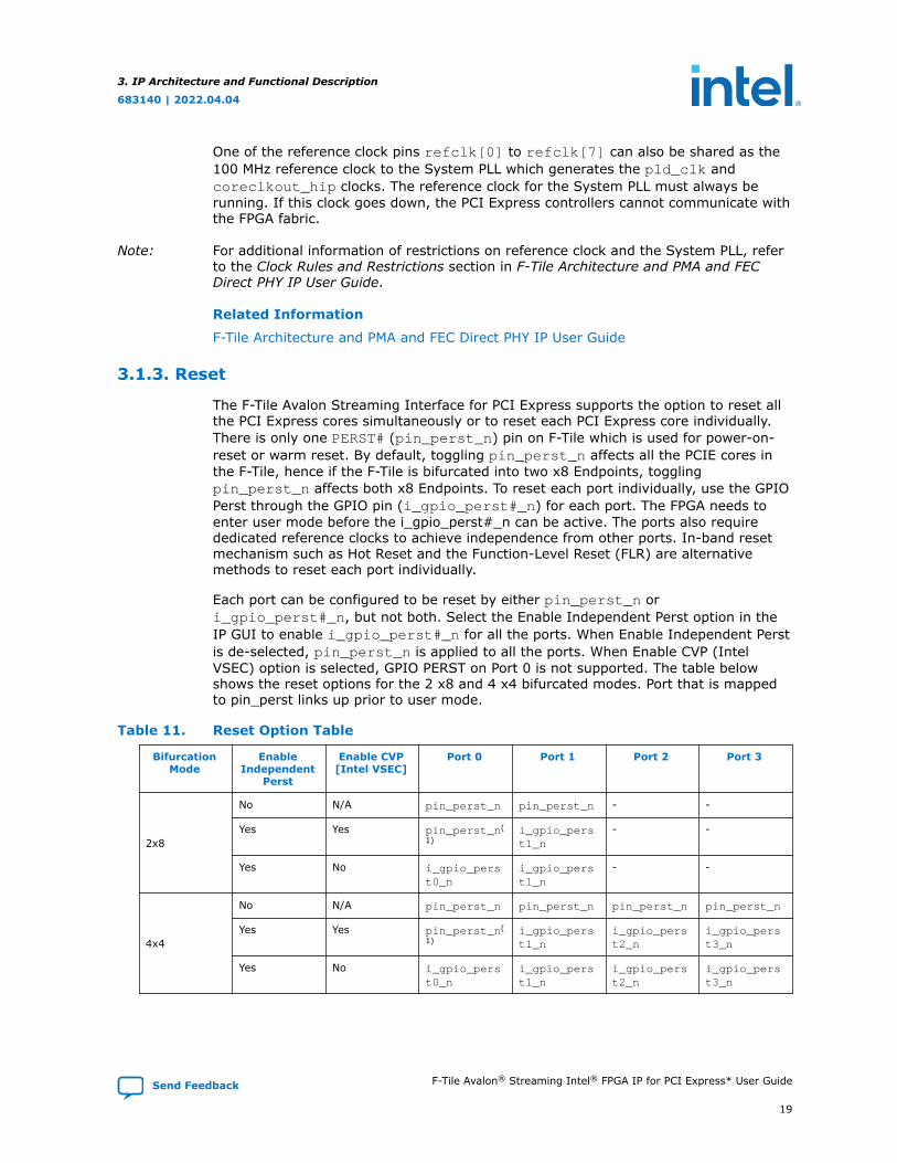
3.1.3. Reset
The F-Tile Avalon Streaming Interface for PCI Express supports the option to reset allthe PCI Express cores simultaneously or to reset each PCI Express core individually.There is only one PERST# (pin_perst_n) pin on F-Tile which is used for power-on-reset or warm reset. By default, toggling pin_perst_n affects all the PCIE cores inthe F-Tile, hence if the F-Tile is bifurcated into two x8 Endpoints, togglingpin_perst_n affects both x8 Endpoints. To reset each port individually, use the GPIOPerst through the GPIO pin (i_gpio_perst#_n) for each port. The FPGA needs toenter user mode before the i_gpio_perst#_n can be active. The ports also requirededicated reference clocks to achieve independence from other ports. In-band resetmechanism such as Hot Reset and the Function-Level Reset (FLR) are alternativemethods to reset each port individually.
Each port can be configured to be reset by either pin_perst_n ori_gpio_perst#_n, but not both. Select the Enable Independent Perst option in theIP GUI to enable i_gpio_perst#_n for all the ports. When Enable Independent Perstis de-selected, pin_perst_n is applied to all the ports. When Enable CVP (IntelVSEC) option is selected, GPIO PERST on Port 0 is not supported. The table belowshows the reset options for the 2 x8 and 4 x4 bifurcated modes. Port that is mappedto pin_perst links up prior to user mode.
Table 11. Reset Option Table
BifurcationMode
EnableIndependent
Perst
Enable CVP[Intel VSEC]
Port 0 Port 1 Port 2 Port 3
2x8
No N/A pin_perst_n pin_perst_n - -
Yes Yes pin_perst_n(1)
i_gpio_perst1_n
- -
Yes No i_gpio_perst0_n
i_gpio_perst1_n
- -
4x4
No N/A pin_perst_n pin_perst_n pin_perst_n pin_perst_n
Yes Yes pin_perst_n(1)
i_gpio_perst1_n
i_gpio_perst2_n
i_gpio_perst3_n
Yes No i_gpio_perst0_n
i_gpio_perst1_n
i_gpio_perst2_n
i_gpio_perst3_n
3. IP Architecture and Functional Description
683140 | 2022.04.04
Send Feedback F-Tile Avalon® Streaming Intel® FPGA IP for PCI Express* User Guide
19
Note: (1): For the mixed pin_perst_n and i_gpio_perst#_n mode, assertingpin_perst_n reset Port 0 only, does not cause a reset on other ports (Port 1 for2x8 bifurcation mode, Port 1 to Port 3 for 4x4 bifurcation mode).
Following are the guidelines for implementing the F-Tile pin_perst_n andi_gpio_perst#_n reset signals:
• pin_perst_n is a "power good" indicator from the associated power domain (towhich F-Tile is connected). When Independent Perst is not enabled, it shall qualifythat the reference clocks driving the refclk0 - refclk3 ports are stable. If oneof the reference clocks becomes stable later, deassert pin_perst_n after thisreference clock becomes stable.
• pin_perst_n assertion is required for proper Autonomous F-Tile functionality. InAutonomous mode, F-Tile can successfully link up upon the release ofpin_perst_n regardless of the FPGA fabric configuration and sends outConfiguration Retry Status (CRS) until the FPGA fabric is configured and ready.
• Avoid trigger pin_perst_n or i_gpio_perst#_n during a Functional LevelReset or before a Functional Level Reset completion. Warm reset or pin_perst_nis allowed 280 µs upon the de-assertion of p#_flr_rcvd_pf_o across all PFswhen Functional Level Reset has been fully acknowledged or completed.Otherwise, the F-Tile PCIe IP configuration may not be reloaded correctly and cancause unexpected behaviour. It is not recoverable until the next warm reset isinitiated.
• The minimum interval requirement between two back-to-back PERST# or GPIOPerst is 500 µs. The minimum interval time required between the deassertion ofthe PERST to the assertion of the next PERST# is 500 µs.
• The reference clock that is used together with pin_perst_n ori_gpio_perst#_n must be stable before pin_perst_n or i_gpio_perst#_nis deactivated.
• No Debug Toolkit access. PHY reconfiguration interface and Hard IP reconfigurationinterface read or write is allowed when the GPIO perst is activated.
Additional information on independent PERST
1. When independent Perst is enabled, clock must be supplied top0_hip_reconfig_clk port.
2. When independent Perst is enabled, you must set bit number 20 of thep0_hip_reconfig_address to 0 when accessing registers throughp0_hip_reconfig_* interface. This is applicable when your design requiresaccess to Hard IP reconfiguration interface for PCIe0 (p#_hip_reconfig_*).
The following is an example where a single PERST# (pin_perst_n) is driven withindependent refclk0 and refclk1. In this example, the add-in card (FPGA and SoC)is powered up first. refclk0 input is fed by the on-board free-running oscillator.refclk1 input driven by the Host becomes stable later. Hence, the PERST# isconnected to the Host.
The following is an example of independent GPIO Perst and reference clocks for eachport. For the instance where the add-in card (FPGA and SoC) is powered up first, it isnot gated by the Perst from the Host System.
3. IP Architecture and Functional Description
683140 | 2022.04.04
F-Tile Avalon® Streaming Intel® FPGA IP for PCI Express* User Guide Send Feedback
20
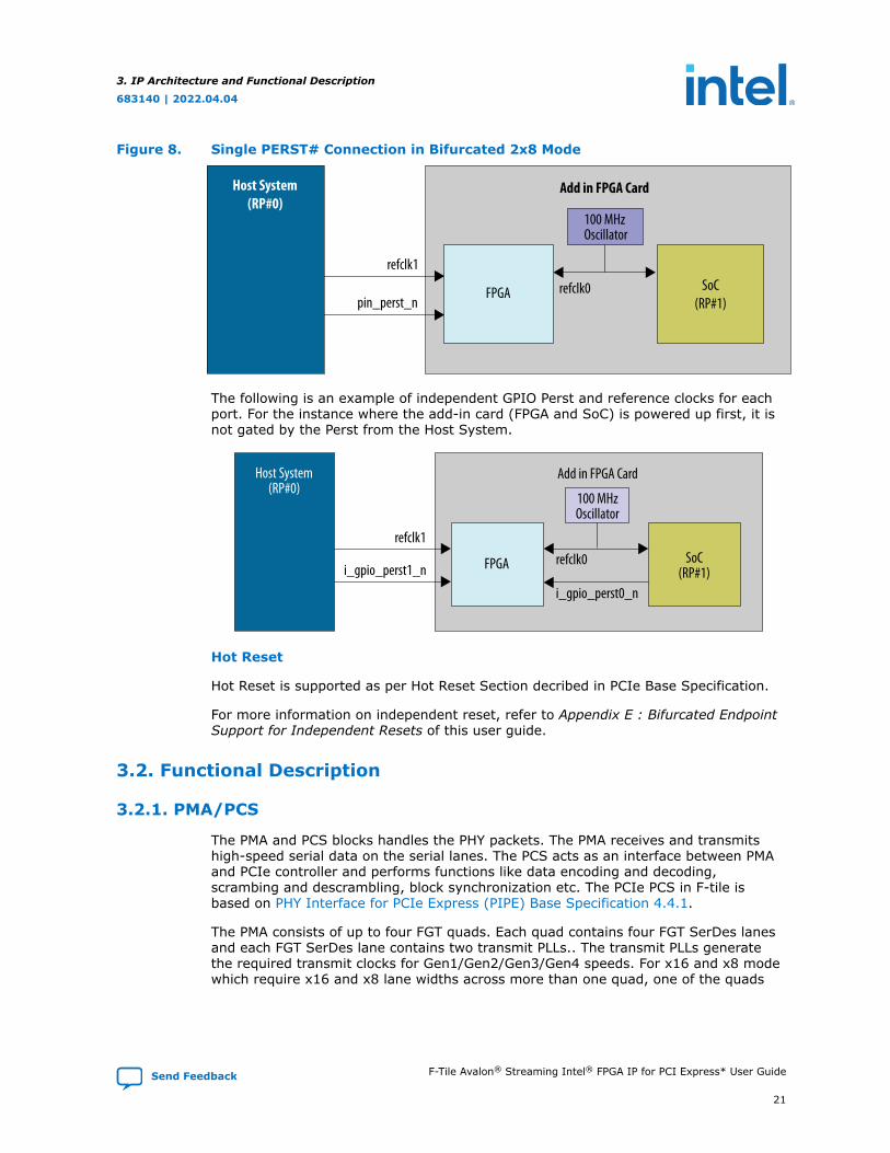
Figure 8. Single PERST# Connection in Bifurcated 2x8 Mode
Add in FPGA Card
FPGA
refclk1
refclk0
100 MHzOscillator
pin_perst_n
Host System(RP#0)
SoC(RP#1)
The following is an example of independent GPIO Perst and reference clocks for eachport. For the instance where the add-in card (FPGA and SoC) is powered up first, it isnot gated by the Perst from the Host System.
refclk0refclk1
i_gpio_perst1_n
Add in FPGA Card
i_gpio_perst0_n
Host System(RP#0)
100 MHzOscillator
SoC(RP#1)
FPGA
Hot Reset
Hot Reset is supported as per Hot Reset Section decribed in PCIe Base Specification.
For more information on independent reset, refer to Appendix E : Bifurcated EndpointSupport for Independent Resets of this user guide.
3.2. Functional Description
3.2.1. PMA/PCS
The PMA and PCS blocks handles the PHY packets. The PMA receives and transmitshigh-speed serial data on the serial lanes. The PCS acts as an interface between PMAand PCIe controller and performs functions like data encoding and decoding,scrambing and descrambling, block synchronization etc. The PCIe PCS in F-tile isbased on PHY Interface for PCIe Express (PIPE) Base Specification 4.4.1.
The PMA consists of up to four FGT quads. Each quad contains four FGT SerDes lanesand each FGT SerDes lane contains two transmit PLLs.. The transmit PLLs generatethe required transmit clocks for Gen1/Gen2/Gen3/Gen4 speeds. For x16 and x8 modewhich require x16 and x8 lane widths across more than one quad, one of the quads
3. IP Architecture and Functional Description
683140 | 2022.04.04
Send Feedback F-Tile Avalon® Streaming Intel® FPGA IP for PCI Express* User Guide
21
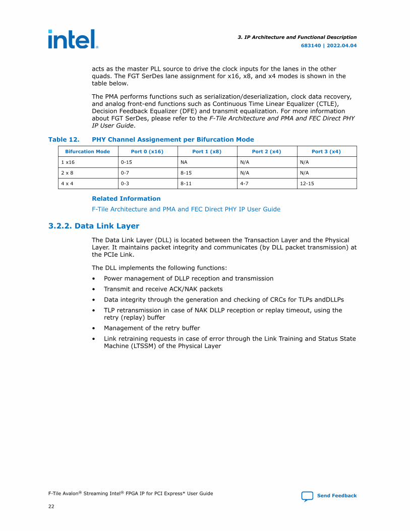
acts as the master PLL source to drive the clock inputs for the lanes in the otherquads. The FGT SerDes lane assignment for x16, x8, and x4 modes is shown in thetable below.
The PMA performs functions such as serialization/deserialization, clock data recovery,and analog front-end functions such as Continuous Time Linear Equalizer (CTLE),Decision Feedback Equalizer (DFE) and transmit equalization. For more informationabout FGT SerDes, please refer to the F-Tile Architecture and PMA and FEC Direct PHYIP User Guide.
Table 12. PHY Channel Assignement per Bifurcation Mode
Bifurcation Mode Port 0 (x16) Port 1 (x8) Port 2 (x4) Port 3 (x4)
1 x16 0-15 NA N/A N/A
2 x 8 0-7 8-15 N/A N/A
4 x 4 0-3 8-11 4-7 12-15
Related Information
F-Tile Architecture and PMA and FEC Direct PHY IP User Guide
3.2.2. Data Link Layer
The Data Link Layer (DLL) is located between the Transaction Layer and the PhysicalLayer. It maintains packet integrity and communicates (by DLL packet transmission) atthe PCIe Link.
The DLL implements the following functions:
• Power management of DLLP reception and transmission
• Transmit and receive ACK/NAK packets
• Data integrity through the generation and checking of CRCs for TLPs andDLLPs
• TLP retransmission in case of NAK DLLP reception or replay timeout, using theretry (replay) buffer
• Management of the retry buffer
• Link retraining requests in case of error through the Link Training and Status StateMachine (LTSSM) of the Physical Layer
3. IP Architecture and Functional Description
683140 | 2022.04.04
F-Tile Avalon® Streaming Intel® FPGA IP for PCI Express* User Guide Send Feedback
22
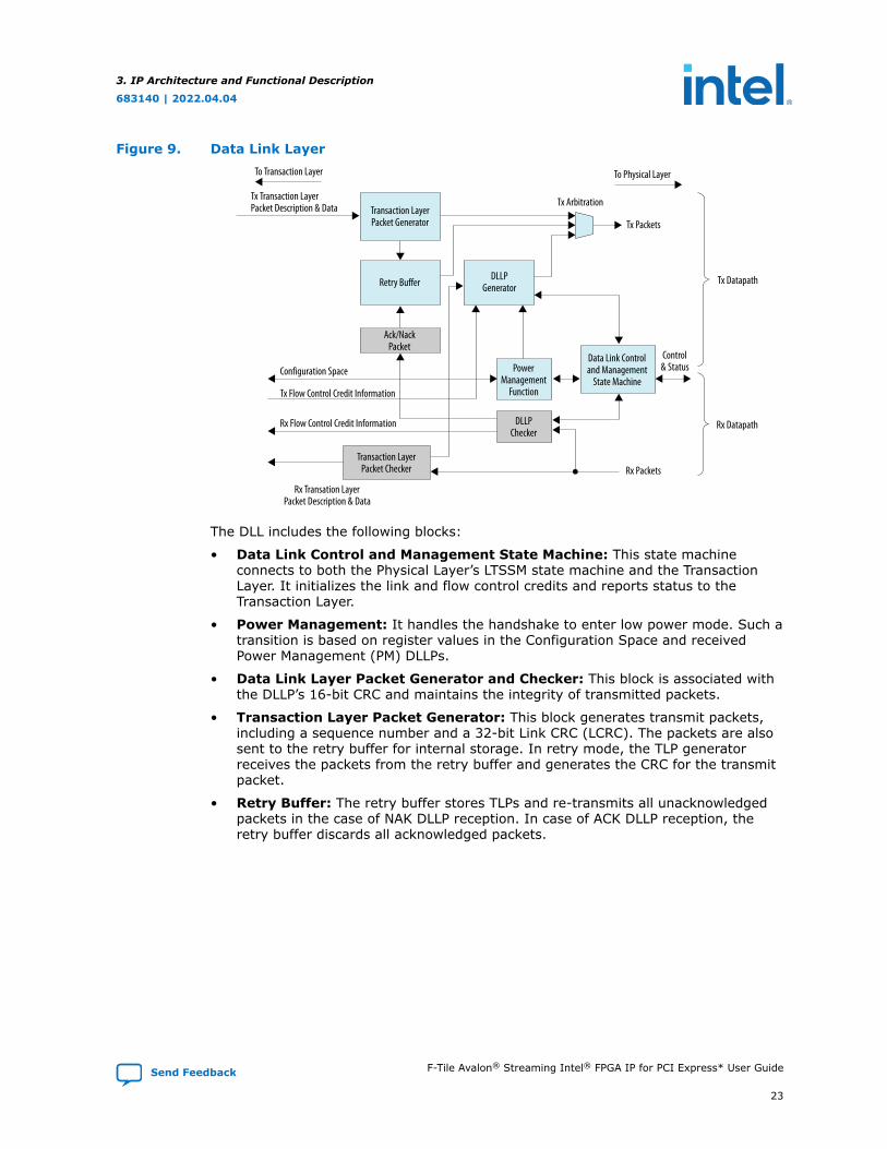
Figure 9. Data Link Layer
Control& Status
Ack/NackPacket
Rx Transation LayerPacket Description & Data
Tx Transaction LayerPacket Description & Data
Configuration Space
Tx Flow Control Credit Information
To Transaction Layer
Rx Flow Control Credit Information
Retry Buffer
Tx Arbitration
To Physical Layer
Tx Packets
Tx Datapath
Rx Datapath
Rx Packets
PowerManagement
Function
DLLPChecker
Transaction LayerPacket Checker
DLLPGenerator
Transaction LayerPacket Generator
Data Link Controland Management
State Machine
The DLL includes the following blocks:
• Data Link Control and Management State Machine: This state machineconnects to both the Physical Layer’s LTSSM state machine and the TransactionLayer. It initializes the link and flow control credits and reports status to theTransaction Layer.
• Power Management: It handles the handshake to enter low power mode. Such atransition is based on register values in the Configuration Space and receivedPower Management (PM) DLLPs.
• Data Link Layer Packet Generator and Checker: This block is associated withthe DLLP’s 16-bit CRC and maintains the integrity of transmitted packets.
• Transaction Layer Packet Generator: This block generates transmit packets,including a sequence number and a 32-bit Link CRC (LCRC). The packets are alsosent to the retry buffer for internal storage. In retry mode, the TLP generatorreceives the packets from the retry buffer and generates the CRC for the transmitpacket.
• Retry Buffer: The retry buffer stores TLPs and re-transmits all unacknowledgedpackets in the case of NAK DLLP reception. In case of ACK DLLP reception, theretry buffer discards all acknowledged packets.
3. IP Architecture and Functional Description
683140 | 2022.04.04
Send Feedback F-Tile Avalon® Streaming Intel® FPGA IP for PCI Express* User Guide
23
• ACK/NAK Packets: The ACK/NAK block handles ACK/NAK DLLPs and generatesthe sequence number of transmitted packets.
• Transaction Layer Packet Checker: This block checks the integrity of thereceived TLP and generates a request for transmission of an ACK/NAK DLLP.
• TX Arbitration: This block arbitrates transactions, prioritizing in the followingorder:
— Initialize FC Data Link Layer packet
— ACK/NAK DLLP (high priority)
— Update FC DLLP (high priority)
— PM DLLP
— Retry buffer TLP
— TLP
— Update FC DLLP (low priority)
— ACK/NAK FC DLLP (low priority)
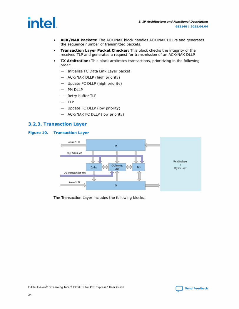
3.2.3. Transaction Layer
Figure 10. Transaction Layer
Avalon-ST RX
Avalon-ST TX
User Avalon-MM
CPL Timeout Avalon-MM
RASCPL Timeout
LogicConfig
RX
Data Link Layer+
Physical Layer
TX
The Transaction Layer includes the following blocks:
3. IP Architecture and Functional Description
683140 | 2022.04.04
F-Tile Avalon® Streaming Intel® FPGA IP for PCI Express* User Guide Send Feedback
24
• Reliability, Availability, and Serviceability (RAS) block: It includes a set offeatures to maintain the integrity of the link.
— Transaction Layer inserts an optional ECRC in the transmit logic and checks itin the receive logic to provide End-to-End data protection.
— When application logic sets TLP Digest (TD) bit in the header of TX TLP, ECRCappends automatically. ECRC generation and checking are not applicable toTLP Bypass Mode.
• TX block: It sends out TX TLPs that it received from application as it is. It alsosends the information about non-posted TLPs to the CPL timeout block for CPLtimeout detection.
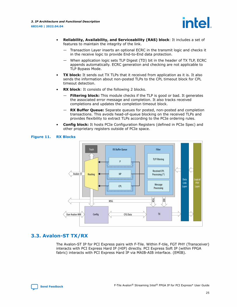
• RX block: It consists of the following 2 blocks.
— Filtering block: This module checks if the TLP is good or bad. It generatesthe associated error message and completion. It also tracks receivedcompletions and updates the completion timeout block.
— RX Buffer Queue: Separate queues for posted, non-posted and completiontransactions. This avoids head-of-queue blocking on the received TLPs andprovides flexibility to extract TLPs according to the PCIe ordering rules.
• Config block: It hosts PCIe Configuration Registers (defined in PCIe Spec) andother proprietary registers outside of PCIe space.
Figure 11. RX Blocks
Config CFG Data
LogicalPHY
Layer
DataLink
Layer
TX
MSG MSG
RX Buffer QueueTrash Filter
TLP Filtering
Received CPLProcessing (*)
MessageProcessing
NP
P
CPL
Avalon-ST
User Avalon-MM
Routing
ERR
3.3. Avalon-ST TX/RX
The Avalon-ST IP for PCI Express pairs with F-Tile. Within F-tile, FGT PHY (Transceiver)interacts with PCI Express Hard IP (HIP) directly. PCI Express Soft IP (within FPGAfabric) interacts with PCI Express Hard IP via MAIB-AIB interface. (EMIB).
3. IP Architecture and Functional Description
683140 | 2022.04.04
Send Feedback F-Tile Avalon® Streaming Intel® FPGA IP for PCI Express* User Guide
25
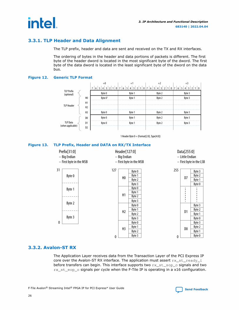
3.3.1. TLP Header and Data Alignment
The TLP prefix, header and data are sent and received on the TX and RX interfaces.
The ordering of bytes in the header and data portions of packets is different. The firstbyte of the header dword is located in the most significant byte of the dword. The firstbyte of the data dword is located in the least significant byte of the dword on the databus.
Figure 12. Generic TLP Format+0
7 6 5 4 3 2 1 0 7 6 5 4 3 2 1 0 7 6 5 4 3 2 1 0 7 6 5 4 3 2 1 0
H0
Byte 0TLP Prefix(optional)
TLP Data(when applicable)
TLP Header
Byte 0
Byte 0
Byte 0
Byte 01
Byte 1
Byte 1
Byte 1
Byte 1
1 Header Byte 0 = {Format[2:0], Type[4:0]}
Byte 1
Byte 2
Byte 2
Byte 2
Byte 2
Byte 2
Byte 3
Byte 3
Byte 3
Byte 3
Byte 3
H1H2
H3
D0
D1
D2
+1 +2 +3
Figure 13. TLP Prefix, Header and DATA on RX/TX Interface
H2
H3
H1
H0
Byte 0Byte 1Byte 2Byte 3Byte 0Byte 1Byte 2Byte 3Byte 0
Byte 2Byte 3Byte 0
Byte 2Byte 1
Byte 3
Byte 1
127
0
Byte 031
0
Byte 1
Byte 2
Byte 3
Prefix[31:0]– Big Endian– First byte in the MSB
Header[127:0]– Big Endian– First byte in the MSB
D1
D0
D7
Byte 3Byte 2Byte 1Byte 0
Byte 3
Byte 1Byte 0Byte 3
Byte 1Byte 2
Byte 0
Byte 2
255
0
Data[255:0]– Little Endian– First byte in the LSB
3.3.2. Avalon-ST RX
The Application Layer receives data from the Transaction Layer of the PCI Express IPcore over the Avalon-ST RX interface. The application must assert rx_st_ready_ibefore transfers can begin. This interface supports two rx_st_sop_o signals and tworx_st_eop_o signals per cycle when the F-Tile IP is operating in a x16 configuration.
3. IP Architecture and Functional Description
683140 | 2022.04.04
F-Tile Avalon® Streaming Intel® FPGA IP for PCI Express* User Guide Send Feedback
26
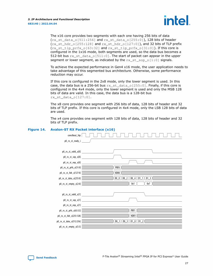
The x16 core provides two segments with each one having 256 bits of data(rx_st_data_o[511:256] and rx_st_data_o[255:0]), 128 bits of header(rx_st_hdr_o[255:128] and rx_st_hdr_o[127:0]), and 32 bits of TLP prefix(rx_st_tlp_prfx_o[63:32] and rx_st_tlp_prfx_o[31:0]). If this core isconfigured in the 1x16 mode, both segments are used, so the data bus becomes a512-bit bus rx_st_data_o[511:0]. The start of packet can appear in the uppersegment or lower segment, as indicated by the rx_st_sop_o[1:0] signals.
To achieve the expected performance in Gen4 x16 mode, the user application needs totake advantage of this segmented bus architecture. Otherwise, some performancereduction may occur.
If this core is configured in the 2x8 mode, only the lower segment is used. In thiscase, the data bus is a 256-bit bus rx_st_data_o[255:0]. Finally, if this core isconfigured in the 4x4 mode, only the lower segment is used and only the MSB 128bits of data are valid. In this case, the data bus is a 128-bit busrx_st_data_o[127:0].
The x8 core provides one segment with 256 bits of data, 128 bits of header and 32bits of TLP prefix. If this core is configured in 4x4 mode, only the LSB 128 bits of dataare used.
The x4 core provides one segment with 128 bits of data, 128 bits of header and 32bits of TLP prefix.
Figure 14. Avalon-ST RX Packet interface (x16)
PRF1
PRF0
HDR0
D0_0 D0_2 D0_4 D1_1 D1_3
0x1 0x7
HDR1
D0_1 D0_3 D1_0 D1_2
coreclkout_hip
p0_rx_st_ready_i
p0_rx_st_valid_o[0]
p0_rx_st_sop_o[0]
p0_rx_st_eop_o[0]
p0_rx_st_prfx_o[31:0]
p0_rx_st_hdr_o[127:0]
p0_rx_st_data_o[255:0]
p0_rx_st_empty_o[2:0]
p0_rx_st_valid_o[1]
p0_rx_st_sop_o[1]
p0_rx_st_eop_o[1]
p0_rx_st_prfx_o[63:32]
p0_rx_st_hdr_o[255:128]
p0_rx_st_data_o[512:256]
p0_rx_st_empty_o[5:3]
3. IP Architecture and Functional Description
683140 | 2022.04.04
Send Feedback F-Tile Avalon® Streaming Intel® FPGA IP for PCI Express* User Guide
27
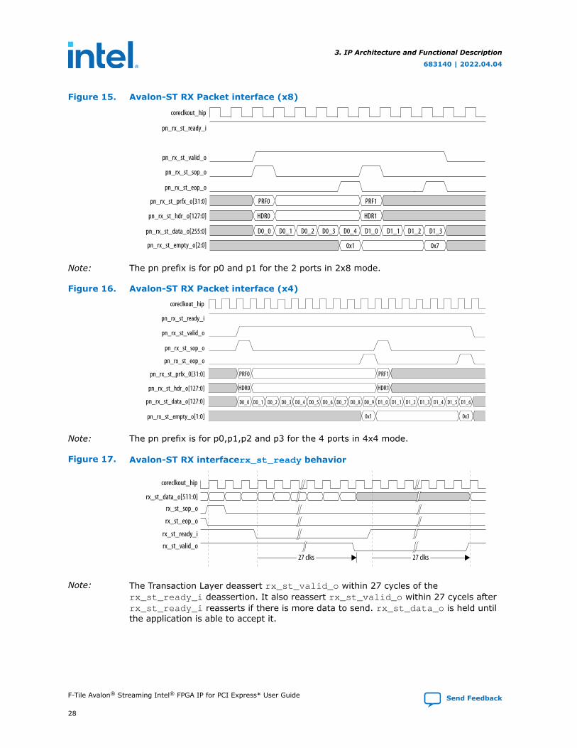
Figure 15. Avalon-ST RX Packet interface (x8)
HDR0 HDR1
PRF0 PRF1
D0_0 D0_1 D0_2 D0_3 D0_4 D1_0 D1_1 D1_2 D1_3
0x1 0x7
coreclkout_hip
pn_rx_st_ready_i
pn_rx_st_valid_o
pn_rx_st_sop_o
pn_rx_st_eop_o
pn_rx_st_prfx_o[31:0]
pn_rx_st_hdr_o[127:0]
pn_rx_st_data_o[255:0]
pn_rx_st_empty_o[2:0]
Note: The pn prefix is for p0 and p1 for the 2 ports in 2x8 mode.
Figure 16. Avalon-ST RX Packet interface (x4)
coreclkout_hip
pn_rx_st_ready_i
pn_rx_st_valid_o
pn_rx_st_sop_o
pn_rx_st_eop_o
pn_rx_st_prfx_0[31:0]
pn_rx_st_hdr_o[127:0]
pn_rx_st_data_o[127:0]
pn_rx_st_empty_o[1:0]
PRF0
HDR0
PRF1
HDR1
D0_0 D0_1 D0_2 D0_3 D0_4 D0_5 D0_6 D0_7 D0_8 D0_9 D1_0 D1_1 D1_2 D1_3 D1_4 D1_5 D1_6
0x30x1
Note: The pn prefix is for p0,p1,p2 and p3 for the 4 ports in 4x4 mode.
Figure 17. Avalon-ST RX interfacerx_st_ready behavior
coreclkout_hip
rx_st_data_o[511:0]
rx_st_eop_o
rx_st_sop_o
rx_st_ready_i
rx_st_valid_o27 clks 27 clks
Note: The Transaction Layer deassert rx_st_valid_o within 27 cycles of therx_st_ready_i deassertion. It also reassert rx_st_valid_o within 27 cycels afterrx_st_ready_i reasserts if there is more data to send. rx_st_data_o is held untilthe application is able to accept it.
3. IP Architecture and Functional Description
683140 | 2022.04.04
F-Tile Avalon® Streaming Intel® FPGA IP for PCI Express* User Guide Send Feedback
28
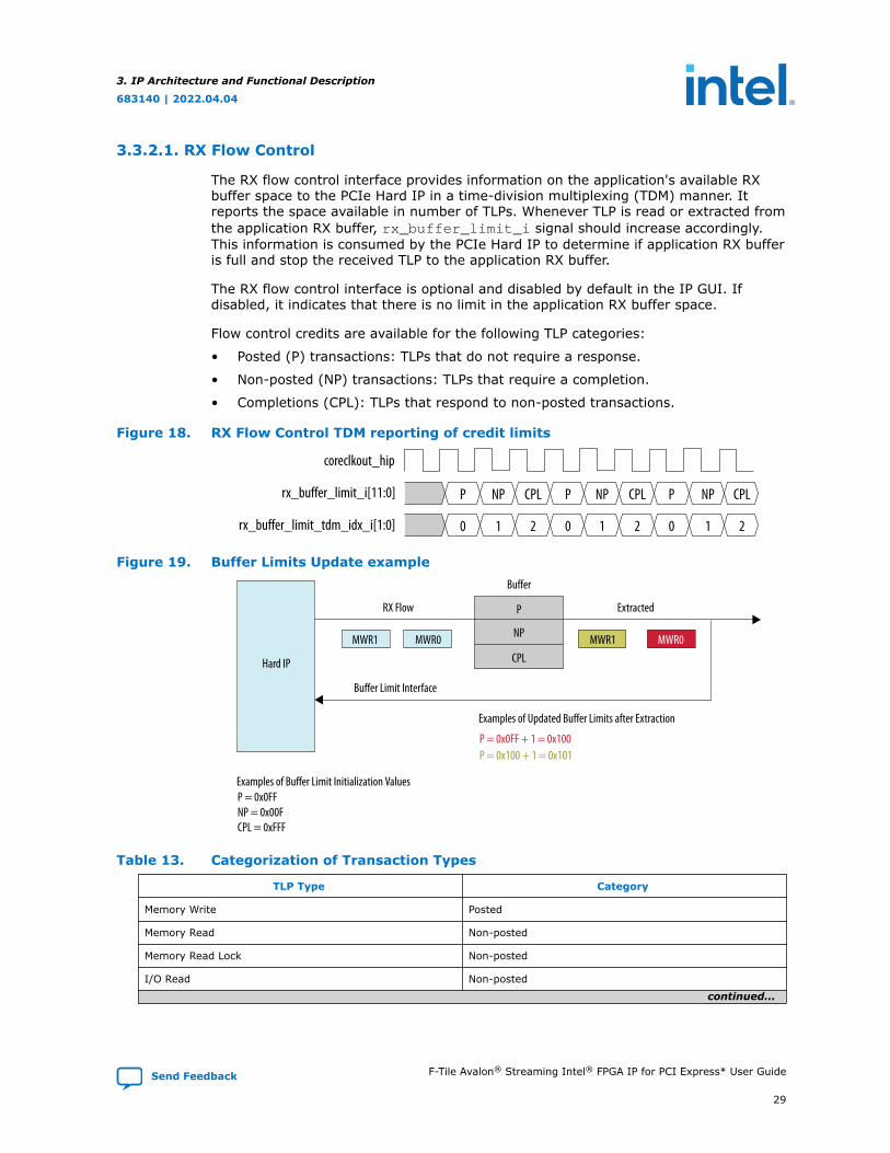
3.3.2.1. RX Flow Control
The RX flow control interface provides information on the application's available RXbuffer space to the PCIe Hard IP in a time-division multiplexing (TDM) manner. Itreports the space available in number of TLPs. Whenever TLP is read or extracted fromthe application RX buffer, rx_buffer_limit_i signal should increase accordingly.This information is consumed by the PCIe Hard IP to determine if application RX bufferis full and stop the received TLP to the application RX buffer.
The RX flow control interface is optional and disabled by default in the IP GUI. Ifdisabled, it indicates that there is no limit in the application RX buffer space.
Flow control credits are available for the following TLP categories:
• Posted (P) transactions: TLPs that do not require a response.
• Non-posted (NP) transactions: TLPs that require a completion.
• Completions (CPL): TLPs that respond to non-posted transactions.
Figure 18. RX Flow Control TDM reporting of credit limits
coreclkout_hip
rx_buffer_limit_i[11:0]
rx_buffer_limit_tdm_idx_i[1:0]
P NP CPL P NP CPL P NP CPL
0 1 2 0 1 2 0 1 2
Figure 19. Buffer Limits Update exampleBuffer
P
NP
RX Flow Extracted
Buffer Limit Interface
CPL
Examples of Updated Buffer Limits after Extraction
P = 0x0FF + 1 = 0x100P = 0x100 + 1 = 0x101
Examples of Buffer Limit Initialization ValuesP = 0x0FFNP = 0x00FCPL = 0xFFF
Hard IP
MWR0MWR1 MWR0MWR1
Table 13. Categorization of Transaction Types
TLP Type Category
Memory Write Posted
Memory Read Non-posted
Memory Read Lock Non-posted
I/O Read Non-posted
continued...
3. IP Architecture and Functional Description
683140 | 2022.04.04
Send Feedback F-Tile Avalon® Streaming Intel® FPGA IP for PCI Express* User Guide
29
TLP Type Category
I/O Write Non-posted
Configuration Read Non-posted
Configuration Write Non-posted
Message Posted
Completion Completion
Completion with Data Completion
Completion Lock Completion
Completion Lock with Data Completion
Fetch and Add AtomicOp Non-posted
Table 14. Credit Advertised by F-Tile PCIe Hard IP
RX BufferSegment
x16 Core (Port0) x8 Core (Port1) x4 Core (Port2/3)
Scaled FlowControldisabled(Credit)
Scaled FlowControl
enabled (ScaleFactor ,Credit)
Scaled FlowControldisabled(Credit)
Scaled FlowControl
enabled (ScaleFactor ,Credit)
Scaled FlowControldisabled(Credit)
Scaled FlowControl
enabled (ScaleFactor ,Credit)
Posted Headers 127 3 , 49 127 2 , 98 127 2 , 56
Posted Data 1456 1 , 1456 760 1 , 760 444 1 , 444
Non-postedHeaders
127 3 , 49 127 2 , 98 127 2 , 56
Non-postedData
392 1 , 392 196 1 , 196 112 1, 112
3.3.3. Avalon-ST TX
The Application Layer transfers data to the Transaction Layer of the PCI Express IPcore over the Avalon-ST TX interface. The Transaction Layer must asserttx_st_ready_o before transmission begins. Transmission of a packet must beuninterrupted when tx_st_ready_o is asserted.
This 512-bit interface supports two locations for the beginning of a TLP, bit[0] andbit[256]. The interface supports multiple TLPs per cycle only when an end-of-packetcycle occurs in the lower 256 bits.
This interface supports two tx_st_sop_i signals and two tx_st_eop_i signals percycle when the F-Tile IP is operating in a x16 configuration. It also does not follow afixed latency between the tx_st_ready_o and tx_st_valid_i[1:0] signals. Datacan be received any time within the defined readyLatency, which is threecoreclkout_hip cycles.
The x16 core provides two segments with each one having 256 bits of data(tx_st_data_i[511:256] and tx_st_data_i[255:0]), 128 bits of header(tx_st_hdr_i[255:128] and tx_st_hdr_i[127:0]), and 32 bits of TLP prefix(tx_st_tlp_prfx_i[63:32] and tx_st_tlp_prfx_i[31:0]). If this core is
3. IP Architecture and Functional Description
683140 | 2022.04.04
F-Tile Avalon® Streaming Intel® FPGA IP for PCI Express* User Guide Send Feedback
30
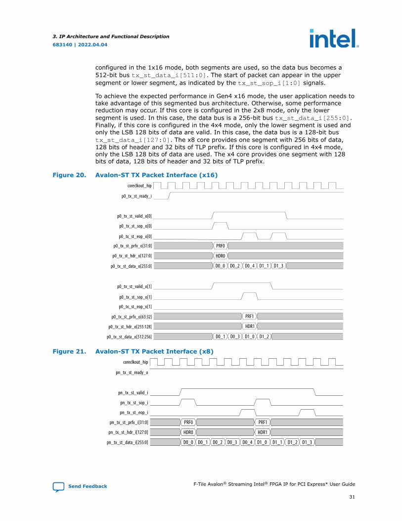
configured in the 1x16 mode, both segments are used, so the data bus becomes a512-bit bus tx_st_data_i[511:0]. The start of packet can appear in the uppersegment or lower segment, as indicated by the tx_st_sop_i[1:0] signals.
To achieve the expected performance in Gen4 x16 mode, the user application needs totake advantage of this segmented bus architecture. Otherwise, some performancereduction may occur. If this core is configured in the 2x8 mode, only the lowersegment is used. In this case, the data bus is a 256-bit bus tx_st_data_i[255:0].Finally, if this core is configured in the 4x4 mode, only the lower segment is used andonly the LSB 128 bits of data are valid. In this case, the data bus is a 128-bit bustx_st_data_i[127:0]. The x8 core provides one segment with 256 bits of data,128 bits of header and 32 bits of TLP prefix. If this core is configured in 4x4 mode,only the LSB 128 bits of data are used. The x4 core provides one segment with 128bits of data, 128 bits of header and 32 bits of TLP prefix.
Figure 20. Avalon-ST TX Packet Interface (x16)coreclkout_hip
p0_tx_st_ready_i
p0_tx_st_valid_o[0]
p0_tx_st_sop_o[0]
p0_tx_st_eop_o[0]
p0_tx_st_prfx_o[31:0]
p0_tx_st_hdr_o[127:0]
p0_tx_st_data_o[255:0]
p0_tx_st_valid_o[1]
p0_tx_st_sop_o[1]
p0_tx_st_eop_o[1]
p0_tx_st_prfx_o[63:32]
p0_tx_st_hdr_o[255:128]
p0_tx_st_data_o[512:256]
PRF0
HDR0
D0_0 D0_2 D0_4 D1_1 D1_3
PRF1
HDR1
D0_1 D0_3 D1_0 D1_2
Figure 21. Avalon-ST TX Packet Interface (x8)
coreclkout_hip
pn_tx_st_ready_o
pn_tx_st_valid_i
pn_tx_st_sop_i
pn_tx_st_eop_i
pn_tx_st_prfx_i[31:0]
pn_tx_st_hdr_i[127:0]
pn_tx_st_data_i[255:0]
PRF0 PRF1
HDR0 HDR1
D0_0 D0_1 D0_2 D0_3 D0_4 D1_0 D1_1 D1_2 D1_3
3. IP Architecture and Functional Description
683140 | 2022.04.04
Send Feedback F-Tile Avalon® Streaming Intel® FPGA IP for PCI Express* User Guide
31
Note: The pn prefix is for p0 and p1 for the 2 ports in 2x8 mode.
Figure 22. Avalon-ST TX Packet Interface (x4)coreclkout_hip
pn_tx_st_ready_o
pn_tx_st_valid_i
pn_tx_st_sop_i
pn_tx_st_eop_i
pn_tx_st_prfx_i[31:0]
pn_tx_st_hdr_i[127:0]
pn_tx_st_data_i[127:0]
PRF0 PRF1
HDR0 HDR1
D0_0 D0_1 D0_2 D0_3 D0_4 D0_5 D0_6 D0_7 D0_8 D0_9 D1_0 D1_1 D1_2 D1_3 D1_4 D1_5 D1_6
Note: The pn prefix is for p0,p1,p2 and p3 for the 4 ports in 4x4 mode.
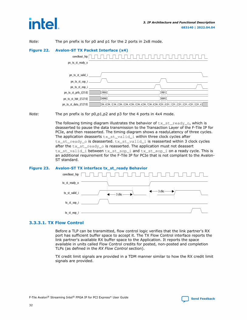
The following timing diagram illustrates the behavior of tx_st_ready_o, which isdeasserted to pause the data transmission to the Transaction Layer of the F-Tile IP forPCIe, and then reasserted. The timing diagram shows a readyLatency of three cycles.The application deasserts tx_st_valid_i within three clock cycles aftertx_st_ready_o is deasserted. tx_st_valid_i is reasserted within 3 clock cyclesafter the tx_st_ready_o is reasserted. The application must not deasserttx_st_valid_i between tx_st_sop_i and tx_st_eop_i on a ready cycle. This isan additional requirement for the F-Tile IP for PCIe that is not compliant to the Avalon-ST standard.
Figure 23. Avalon-ST TX interface tx_st_ready Behavior
3 clks3 clks
coreclkout_hip
tx_st_ready_o
tx_st_valid_i
tx_st_eop_i
tx_st_sop_i
3.3.3.1. TX Flow Control
Before a TLP can be transmitted, flow control logic verifies that the link partner's RXport has sufficient buffer space to accept it. The TX Flow Control interface reports thelink partner's available RX buffer space to the Application. It reports the spaceavailable in units called Flow Control credits for posted, non-posted and completionTLPs (as defined in the RX Flow Control section).
TX credit limit signals are provided in a TDM manner similar to how the RX credit limitsignals are provided.
3. IP Architecture and Functional Description
683140 | 2022.04.04
F-Tile Avalon® Streaming Intel® FPGA IP for PCI Express* User Guide Send Feedback
32
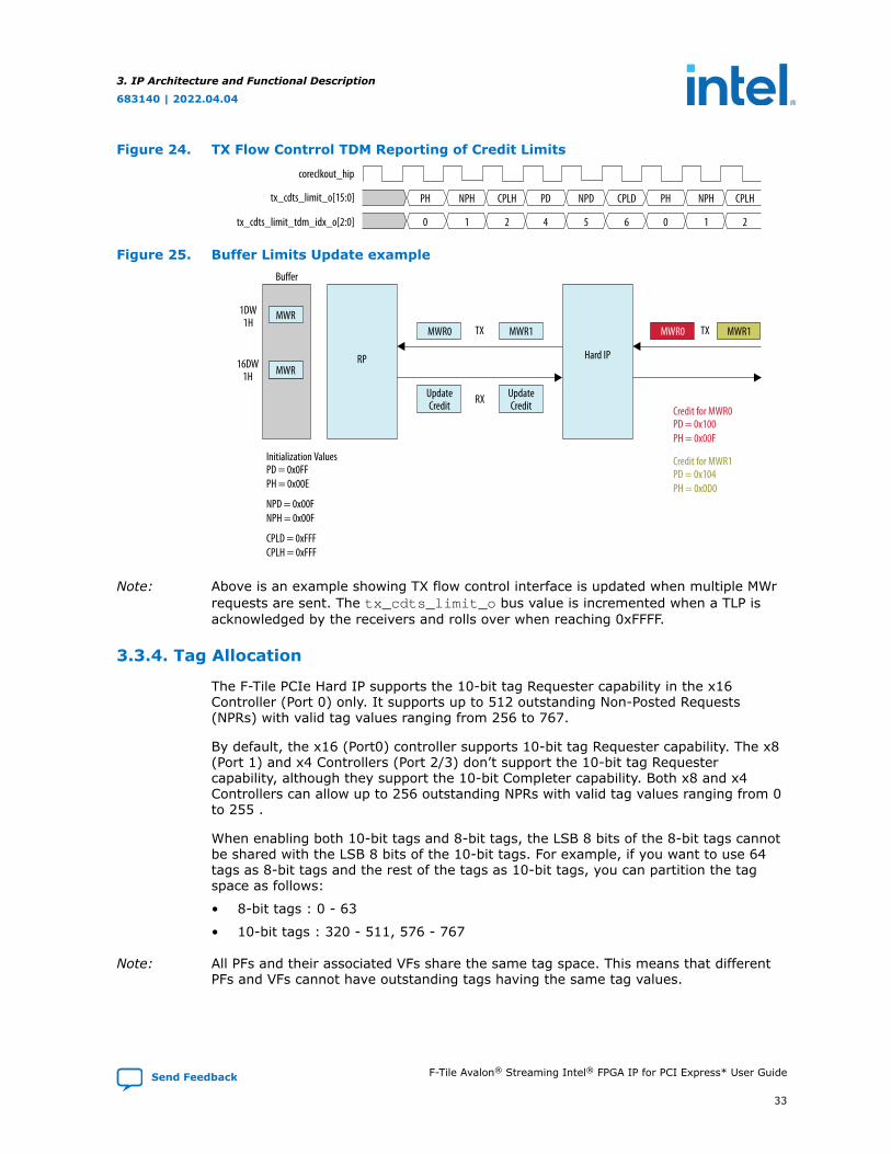
Figure 24. TX Flow Contrrol TDM Reporting of Credit Limits
PH NPH CPLH PD NPD CPLD PH NPH CPLH
0 1 2 4 5 6 0 1 2
coreclkout_hip
tx_cdts_limit_tdm_idx_o[2:0]
tx_cdts_limit_o[15:0]
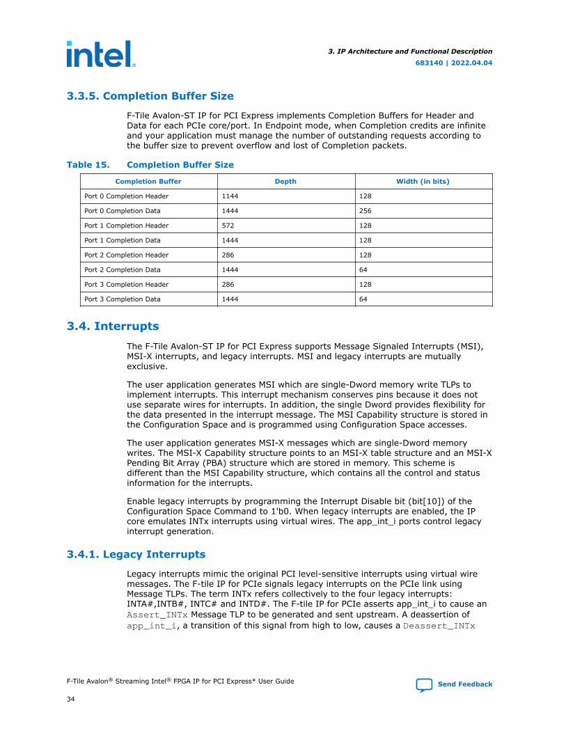
Figure 25. Buffer Limits Update example
MWRMWR0 MWR1TX MWR1TX
UpdateCredit
UpdateCreditRX
RP Hard IPMWR
Buffer
Initialization ValuesPD = 0x0FFPH = 0x00E
NPD = 0x00FNPH = 0x00F
CPLD = 0xFFFCPLH = 0xFFF
Credit for MWR0PD = 0x100PH = 0x00F
Credit for MWR1PD = 0x104PH = 0x0D0
1DW1H
16DW1H
MWR0
Note: Above is an example showing TX flow control interface is updated when multiple MWrrequests are sent. The tx_cdts_limit_o bus value is incremented when a TLP isacknowledged by the receivers and rolls over when reaching 0xFFFF.
3.3.4. Tag Allocation
The F-Tile PCIe Hard IP supports the 10-bit tag Requester capability in the x16Controller (Port 0) only. It supports up to 512 outstanding Non-Posted Requests(NPRs) with valid tag values ranging from 256 to 767.
By default, the x16 (Port0) controller supports 10-bit tag Requester capability. The x8(Port 1) and x4 Controllers (Port 2/3) don’t support the 10-bit tag Requestercapability, although they support the 10-bit Completer capability. Both x8 and x4Controllers can allow up to 256 outstanding NPRs with valid tag values ranging from 0to 255 .
When enabling both 10-bit tags and 8-bit tags, the LSB 8 bits of the 8-bit tags cannotbe shared with the LSB 8 bits of the 10-bit tags. For example, if you want to use 64tags as 8-bit tags and the rest of the tags as 10-bit tags, you can partition the tagspace as follows:
• 8-bit tags : 0 - 63
• 10-bit tags : 320 - 511, 576 - 767
Note: All PFs and their associated VFs share the same tag space. This means that differentPFs and VFs cannot have outstanding tags having the same tag values.
3. IP Architecture and Functional Description
683140 | 2022.04.04
Send Feedback F-Tile Avalon® Streaming Intel® FPGA IP for PCI Express* User Guide
33
3.3.5. Completion Buffer Size
F-Tile Avalon-ST IP for PCI Express implements Completion Buffers for Header andData for each PCIe core/port. In Endpoint mode, when Completion credits are infiniteand your application must manage the number of outstanding requests according tothe buffer size to prevent overflow and lost of Completion packets.
Table 15. Completion Buffer Size
Completion Buffer Depth Width (in bits)
Port 0 Completion Header 1144 128
Port 0 Completion Data 1444 256
Port 1 Completion Header 572 128
Port 1 Completion Data 1444 128
Port 2 Completion Header 286 128
Port 2 Completion Data 1444 64
Port 3 Completion Header 286 128
Port 3 Completion Data 1444 64
3.4. Interrupts
The F-Tile Avalon-ST IP for PCI Express supports Message Signaled Interrupts (MSI),MSI-X interrupts, and legacy interrupts. MSI and legacy interrupts are mutuallyexclusive.
The user application generates MSI which are single-Dword memory write TLPs toimplement interrupts. This interrupt mechanism conserves pins because it does notuse separate wires for interrupts. In addition, the single Dword provides flexibility forthe data presented in the interrupt message. The MSI Capability structure is stored inthe Configuration Space and is programmed using Configuration Space accesses.
The user application generates MSI-X messages which are single-Dword memorywrites. The MSI-X Capability structure points to an MSI-X table structure and an MSI-XPending Bit Array (PBA) structure which are stored in memory. This scheme isdifferent than the MSI Capability structure, which contains all the control and statusinformation for the interrupts.
Enable legacy interrupts by programming the Interrupt Disable bit (bit[10]) of theConfiguration Space Command to 1'b0. When legacy interrupts are enabled, the IPcore emulates INTx interrupts using virtual wires. The app_int_i ports control legacyinterrupt generation.
3.4.1. Legacy Interrupts
Legacy interrupts mimic the original PCI level-sensitive interrupts using virtual wiremessages. The F-tile IP for PCIe signals legacy interrupts on the PCIe link usingMessage TLPs. The term INTx refers collectively to the four legacy interrupts:INTA#,INTB#, INTC# and INTD#. The F-tile IP for PCIe asserts app_int_i to cause anAssert_INTx Message TLP to be generated and sent upstream. A deassertion ofapp_int_i, a transition of this signal from high to low, causes a Deassert_INTx
3. IP Architecture and Functional Description
683140 | 2022.04.04
F-Tile Avalon® Streaming Intel® FPGA IP for PCI Express* User Guide Send Feedback
34
Message TLP to be generated and sent upstream. To use legacy interrupts, you mustclear the Interrupt Disable bit, which is bit 10 of the Command Register in theconfiguration header. Then, you must turn off the MSI Enable bit.
Figure 26. Generating an Assert_INTx Message TLP Using the app_int_i Signal
coreclkout_hip
app_int[0]
Note: app_int_i[0] is asserted for at least eight clock cycles to cause an Assert_INTxMessage TLP to be generated and sent upstream for physical function 0. For amultifunctions implementation, app_int_i[0] is for physical function 0,app_int_i[1] is for physical function 1 and so on. Deasserting a app_int_i signalby driving it from high to low causes a Deassert_INTx Message TLP to be generatedand sent upstream.
3.4.2. MSI
MSI interrupts are signaled on the PCI Express link using a single dword Memory WriteTLP. The user application issues an MSI request (MWr) through the Avalon-ST interfaceand updates the configuration space register using the MSI interface.
The Mask Bits register and Pending Bits register are 32 bits in length each, with eachpotential interrupt message having its own mask bit and pending bit. If bit[0] of theMask Bits register is set, interrupt message 0 is masked. When an interrupt messageis masked, the MSI for that vector cannot be sent. If software clears the mask bit andthe corresponding pending bit is set, the function must send the MSI request at thattime.
You should obtain the necessary MSI information (such as the message address anddata) from the configuration output interface (tl_cfg_*) to create the MWr TLP in theformat shown below to be sent via the Avalon-ST interface.
3. IP Architecture and Functional Description
683140 | 2022.04.04
Send Feedback F-Tile Avalon® Streaming Intel® FPGA IP for PCI Express* User Guide
35
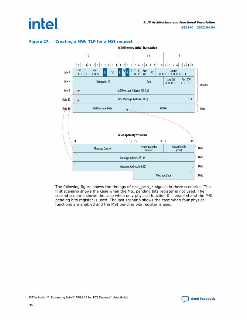
Figure 27. Creating a MWr TLP for a MSI request
7 6 5 4 3 2 1 0 7 6 5 4 3 2 1 0 7 6 5 4 3 2 1 0 7 6 5 4 3 2 1 0
MSI (Memory Write) Transaction
MSI Capability Structure
Fmt
+0 +1 +2 +3
Byte 0
Byte 4
Byte 8
Byte 12
Byte 16
TypeTC ATAt
trLength
0 0 0 0 0 0 0 0 0 10 1 1 0 0 0 0 0
Last DW0 0 0 0
0000h
Tag
MSI Message Address [63:32]
MSI Message Address [31:0]
MSI Message Data
Message Control
Message Address [63:32]
Message Data DW3
DW2
DW1
DW0
Message Address [31:0]
Next CapabilityPointer
Capability ID(05h)
0781631 15
Requester ID
0 0
First DW
Header
Data
1 1 1 1
Attr00
TH
TD
EPR R R
The following figure shows the timings of msi_pnd_* signals in three scenarios. Thefirst scenario shows the case when the MSI pending bits register is not used. Thesecond scenario shows the case when only physical function 0 is enabled and the MSIpending bits register is used. The last scenario shows the case when four physicalfunctions are enabled and the MSI pending bits register is used.
3. IP Architecture and Functional Description
683140 | 2022.04.04
F-Tile Avalon® Streaming Intel® FPGA IP for PCI Express* User Guide Send Feedback
36
Figure 28. Timing Diagrams for msi_pnd* Signals
coreclkout_hip
msi_pnd_byte_i[7:0]
msi_pnd_func_i[2:0]
msi_pnd_addr_i[1:0]
coreclkout_hip
msi_pnd_byte_i[7:0]
msi_pnd_func_i[2:0]
msi_pnd_addr_i[1:0]
coreclkout_hip
msi_pnd_byte_i[7:0]
msi_pnd_func_i[2:0]
msi_pnd_addr_i[1:0]
0x0 0x1 0x2 0x3 0x0 0x1 0x2 0x3 0x0 0x1 0x2 0x3 0x0 0x1 0x2 0x3
B0 B1 B2 B3 B0 B1 B2 B3 B0 B1 B2 B3 B0 B1 B2 B3
0x0 0x1 0x0 0x1
0x0 0x1 0x2 0x3 0x0 0x1 0x2 0x3 0x0 0x1 0x2 0x3 0x0 0x1 0x2 0x3
B0 B1 B2 B3 B0 B1 B2 B3 B0 B1 B2 B3 B0 B1 B2 B3
0x0
0x0
0x0
0x0
There are 32 possible MSI messages. The number of messages requested by aparticular component does not necessarily correspond to the number of messagesallocated. For example, in the following figure, the Endpoint requests eight MSIs but isonly allocated two. In this case, you must design the Application Layer to use only twoallocated messages.
Figure 29. MSI Request Example
Endpoint
InterruptBlock
Interrupt Register
8 Requested2 Allocated
Root Complex
RootPort
CPU
The following table describes three example implementations. The first exampleallocates all 32 MSI messages. The second and third examples only allocate 4interrupts.
3. IP Architecture and Functional Description
683140 | 2022.04.04
Send Feedback F-Tile Avalon® Streaming Intel® FPGA IP for PCI Express* User Guide
37
Table 16. MSI Messages Requested, Allocated and Mapped
MSI Allocated
32 4 4
System Error 31 3 3
Hot Plug and PowerManagement Event
30 2 3
Application Layer 29:0 1:0 2:0
MSI interrupts generated for Hot Plug, Power Management Events, and System Errorsalways use Traffic Class 0. MSI interrupts generated by the Application Layer can useany Traffic Class. For example, a DMA that generates an MSI at the end of atransmission use the same traffic control as was used to transfer data.
The following figure illustrates a possible implementation of the Interrupt HandlerModule with a per vector enable bit in the Application Layer. Alternatively, theApplication Layer could implement a global interrupt enable instead of this per vectorMSI.
Figure 30. Implementation Example of the Interrupt Handler Block
IRQGeneration
App Layer
R/W
R/W
Vector 0
Vector 1
Interrupt Enable 0
Interrupt Enable 1
msi_req0
msi_req1
app_int_i
MSI info (from tl_cfg_ctl* /tl_cfg_addr* /tl_cfg_func*)& Master Enable
Avalon-STsingle-dword MWR TLPs
msi_pnd_*
Interrupt Request 0
Interrupt Request 1
Arbitration &TLP Generator
IRQGeneration
App Layer
3.4.3. MSI-X
The F-Tile IP for PCIe provides a Configuration Intercept Interface. User soft logic canmonitor this interface to get MSI-X Enable and MSI-X function mask relatedinformation. User application logic needs to implement the MSI-X tables for all PFs andVFs at the memory space pointed to by the BARs as a part of your Application Layer.
For more details on the MSI-X related information that you can obtain from theConfiguration Intercept Interface, refer to the MSI-X Registers section in theConfiguration Register section.
3. IP Architecture and Functional Description
683140 | 2022.04.04
F-Tile Avalon® Streaming Intel® FPGA IP for PCI Express* User Guide Send Feedback
38
MSI-X is an optional feature that allows the user application to support large amountof vectors with independent message data and address for each vector. When MSI-X issupported, you need to specify the size and the location (BARs and offsets) of theMSI-X table and Pending Bit Array (PBA). MSI-X can support up to 2048 vectors perfunction versus 32 vectors per function for MSI. A function is allowed to send MSI-Xmessages when MSI-X is enabled and the function is not masked. The application usesthe Configuration Output Interface (address 0x0C bit[5:4]) or Configuration InterceptInterface to access this information.
When the application needs to generate an MSI-X, it uses the contents of the MSI-XTable (Address and Data) and generate a Memory Write through the Avalon-STinterface.
If user enable MSI-X interrupt, you should implement the MSI-X table structures atthe memory space pointed to by the BARs as a part of your Application Layer. TheMSI-X Capability Structure contains information about the MSI-X Table and PBAStructure. For example, it contains pointers to the bases of the MSI-X Table and PBAStructure, expressed as offsets from the addresses in the function's BARs. TheMessage Control register within the MSI-X Capability Structure also contains the MSI-X
MSI-X interrupts are standard Memory Writes, therefore Memory Write ordering rulesapply.
Table 17. MSI-X Configuration Example
MSI-X Vector MSI-X Upper Address MSI-X Lower Address MSI-X Data
0 0x00000001 0xAAAA0000 0x00000001
1 0x00000001 0xBBBB0000 0x00000002
2 0x00000001 0xCCCC0000 0x00000003
Table 18. PBA Table Example
PBA Table PBA Entries
Offset 0 0x0
If the application needs to generate an MSI-X interrupt (vector 1), it reads the MSI-XTable information, generates a MWR TLP through the Avalon-ST interface and assertsthe corresponding PBA bits (bit[1]) in a similar fashion as for MSI generation.
The generated TLP is sent to address 0x00000001_BBBB0000 and the data is0x00000002. When the MSI-X has been sent, the application can clear the associatedPBA bits.
The MSI-X capability structure points to the MSI-X Table structure and MSI-X PendingBit Array (PBA) registers. The BIOS sets up the starting address offsets and BARassociated with the pointer to the starting address of the MSI-X Table and PBAregisters.
3. IP Architecture and Functional Description
683140 | 2022.04.04
Send Feedback F-Tile Avalon® Streaming Intel® FPGA IP for PCI Express* User Guide
39
Figure 31. MSI-X Interrupt Component
MSI-X Table
Application Layer
MSI-X PBA
Monitor & Clr
Addr, Data
IRQ Source
IRQProcessor
Host SW Programs Addr,Data and Vector Control
Memory Write TLP
RX RX
PCIe with Avalon-ST I/F
Host
Memory WriteTLP
TX TX
1. Host software sets up the MSI-X interrupts in the Application Layer by completingthe following steps:
• Host software reads the Message Control register at 0x050 register todetermine the MSI-X Table size. The number of table entries is the <valueread> + 1. The maximum table size is 2048 entries. Each 16-byte entry isdivided in 4 fields as shown in the figure below. For multi-function variants,BAR4 accesses the MSI-X table. For all other variants, any BAR can access theMSI-X table. The base address of the MSI-X table must be aligned to a 4 KBboundary.
• The host sets up the MSI-X table. It programs MSI-X address, data, andmasks bits for each entry as shown in the figure below.
Figure 32. Format of MSI-X Table
Vector Control
DWORD 3 DWORD 2 DWORD 1 DWORD 0
Message Data Message Upper Address Message Address
Vector Control Message Upper Address
Entry 0 Base
Vector Control Message Data Message Upper Address Message Address Entry 2 Base + 2 x 16
Entry (N-1) Base + (N-1) x 16
Host Byte Addresses
Vector Control Message Data Message Upper Address Message Address Entry 1 Base + 1 x 16
Message AddressMessage Data
••••••
••••••
•••
• The host calculates the address of the <nth> entry using the followingformula:
nth_address = base address[BAR]+16<n>
2. When Application Layer needs to issue an interrupt, it drives an interrupt requet tothe IRQ Source module.
3. 3. The IRQ Sources sets appropriate bit in the MSI-X PBA table. The PBA can useqword or dword accesses. For qword accesses, the IRQ Source calculates theaddress of the <mth> bit using the following formulas:
qword address = <PBA base addr> + 8(floor(<m>/64))qword bit = <m> mod 64
3. IP Architecture and Functional Description
683140 | 2022.04.04
F-Tile Avalon® Streaming Intel® FPGA IP for PCI Express* User Guide Send Feedback
40
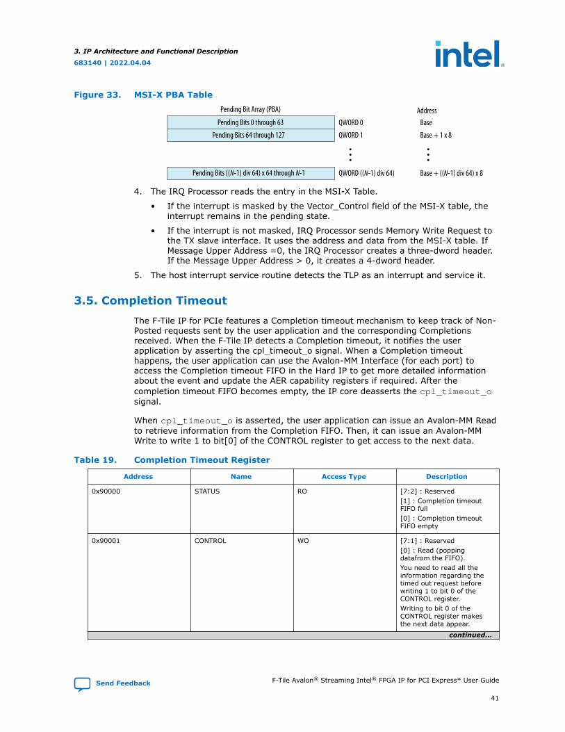
Figure 33. MSI-X PBA TablePending Bit Array (PBA)
Pending Bits 0 through 63
Pending Bits 64 through 127 Base + 1 x 8
Base
QWORD 1
Base + ((N-1) div 64) x 8QWORD ((N-1) div 64)
QWORD 0Address
Pending Bits ((N-1) div 64) x 64 through N-1
••••••
4. The IRQ Processor reads the entry in the MSI-X Table.
• If the interrupt is masked by the Vector_Control field of the MSI-X table, theinterrupt remains in the pending state.
• If the interrupt is not masked, IRQ Processor sends Memory Write Request tothe TX slave interface. It uses the address and data from the MSI-X table. IfMessage Upper Address =0, the IRQ Processor creates a three-dword header.If the Message Upper Address > 0, it creates a 4-dword header.
5. The host interrupt service routine detects the TLP as an interrupt and service it.
3.5. Completion Timeout
The F-Tile IP for PCIe features a Completion timeout mechanism to keep track of Non-Posted requests sent by the user application and the corresponding Completionsreceived. When the F-Tile IP detects a Completion timeout, it notifies the userapplication by asserting the cpl_timeout_o signal. When a Completion timeouthappens, the user application can use the Avalon-MM Interface (for each port) toaccess the Completion timeout FIFO in the Hard IP to get more detailed informationabout the event and update the AER capability registers if required. After thecompletion timeout FIFO becomes empty, the IP core deasserts the cpl_timeout_osignal.
When cpl_timeout_o is asserted, the user application can issue an Avalon-MM Readto retrieve information from the Completion FIFO. Then, it can issue an Avalon-MMWrite to write 1 to bit[0] of the CONTROL register to get access to the next data.
Table 19. Completion Timeout Register
Address Name Access Type Description
0x90000 STATUS RO [7:2] : Reserved[1] : Completion timeoutFIFO full[0] : Completion timeoutFIFO empty
0x90001 CONTROL WO [7:1] : Reserved[0] : Read (poppingdatafrom the FIFO).You need to read all theinformation regarding thetimed out request beforewriting 1 to bit 0 of theCONTROL register.Writing to bit 0 of theCONTROL register makesthe next data appear.
continued...
3. IP Architecture and Functional Description
683140 | 2022.04.04
Send Feedback F-Tile Avalon® Streaming Intel® FPGA IP for PCI Express* User Guide
41

Address Name Access Type Description
0x90002 VF RO [7:0] : vfunc_num[7:0]Virtual Function number forthe VF that initiates thenonposted transaction forwhich the completiontimeout is observed.
0x90003 PF RO [7] : vfunc_active[6] : Reserved[5:3] : func_num[2:0]Physical function number(least significant 8 bits) forthe PF that initiates thenonposted transaction forwhich the completiontimeout is observed.[2:0] : vfunc_num[10:8]Virtual Function number(most significant 3 bits) forthe VF that initiates thememory read request forwhich the completiontimeout is observed.
0x90004 LEN1 RO [7:0] : cpl_lenn[7:0]Transfer length in bytes(least significant 8 bits), ofthe expected completionthat timed out for thenonposted transaction.For a split completion, itindicates the number ofbytes remaining to bedelivered when thecompletion timed out (Maxlength is Max Read requestsize. Example: 4K Bytes=2^12 bytes)
0x90005 LEN2 RO [7:4] : Reserved[3:0] : cpl_lenn[11:8]Transfer length in bytes(most significant 4 bits), ofthe expected completionthat timed out for thenonposted transaction.For a split completion, itindicates the number ofbytes remaining to bedelivered when thecompletion timed out (Maxlength is Max Read requestsize. Example: 4K Bytes=2^12 bytes)
0x90006 TAG1 RO [7:0] : cpl_tag[7:0] Tag ID(least significant 8 bits) ofthe expected completionthat timed out for the non-posted transaction.
0x90007 TAG2 RO [7:5] : cpl_tc[2:0] Trafficclass of the expectedcompletion that timed outfor the non-postedtransaction.
3. IP Architecture and Functional Description
683140 | 2022.04.04
F-Tile Avalon® Streaming Intel® FPGA IP for PCI Express* User Guide Send Feedback
42

Address Name Access Type Description
[4:3] : cpl_attr[1:0]Attribute of the expectedcompletion that timed outfor the non-postedtransaction. ID basedordering is not supported.• [4] -> Relaxed ordering• [3]-> No Snoop• [2] : Reserved[1:0]: cpl_tag[9:8] Tag ID(most significant 2 bits) ofthe expected completionthat timed out for the non-posted transaction.
3.6. Hot Plug
Hot Plug support means that the device can be added to or removed from a systemduring runtime. The Hot Plug Interface in the F-Tile Avalon-ST IP for PCIe allows anIntel FPGA with this IP to safely provide this capability.
Hot Plug interface displays a list of signals reported by the on-board hot plugcomponents in the Downstream Port. This interface is available only if the Slot StatusRegister of the PCI Express Capability Structure is enabled.
3.7. Power Management
Software programs the device into a D-state by writing to the Power ManagementControl and Status register in the PCI Power Management Capability Structure. Thepower management output signals indicate the current power state. The IP coresupports the two mandatory power states: D0 (full power) and D3 (preparation for aloss of power). It does not support the optional D1 and D2 low power states.
The correspondence between the device power states (D states) and link power states(L states) is as follows:
Table 20. Device and Link Power States Relationship
Device Power State Link Power State
D0 L0
D1 (not supported) L1
D2 (not supported) L2
D3 L1, L2/L3 Ready
The F-Tile Avalon Streaming Intel FPGA IP for PCI Express IP core supports therequired D0 and D3 Power Management states. It does not support the optional D1and D2 Power Management states. The software programs the device into a D-stateby writing to the Power Management Control and Status register in the PCI PowerManagement Capability Structure. The power management interface transmits the D-state to the Application Layer.
3. IP Architecture and Functional Description
683140 | 2022.04.04
Send Feedback F-Tile Avalon® Streaming Intel® FPGA IP for PCI Express* User Guide
43
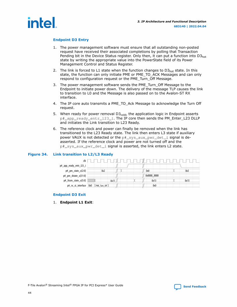
Endpoint D3 Entry
1. The power management software must ensure that all outstanding non-postedrequest have received their associated completions by polling that TransactionPending bit in the Device Status register. Only then, it can put a function into D3hotstate by writing the appropriate value into the PowerState field of its PowerManagement Control and Status Register.
2. The link is forced to L1 state when the function changes to D3hot state. In thisstate, the function can only initiate PME or PME_TO_ACK Messages and can onlyrespond to configuration request or the PME_Turn_Off Message.
3. The power management software sends the PME_Turn_Off Message to theEndpoint to initiate power down. The delivery of the message TLP causes the linkto transition to L0 and the Message is also passed on to the Avalon-ST RXinterface.
4. The IP core auto transmits a PME_TO_Ack Message to acknowledge the Turn Offrequest.
5. When ready for power removal D3cold, the application logic in Endpoint assertsp#_app_ready_entr_l23_i. The IP core then sends the PM_Enter_L23 DLLPand initiates the Link transition to L23 Ready.
6. The reference clock and power can finally be removed when the link hastransitioned to the L23 Ready state. The link then enters L3 state if auxiliarypower VAUX is not detected or the p#_sys_aux_pwr_det_i signal is de-asserted. If the reference clock and power are not turned off and thep#_sys_aux_pwr_det_i signal is asserted, the link enters L2 state.
Figure 34. Link transition to L2/L3 Ready
clk
0x0 0x30x2
0x11 0x13 0x15
0x00x0
0x8888_8888
p#_app_ready_entr_I23_i
p#_pm_state_o[2:0]
p#_Itssm_state_o[5:0]
p#_rx_st_interface
p#_pm_dstate_o[31:0]
PME_Turn_Off
Endpoint D3 Exit
1. Endpoint L1 Exit:
3. IP Architecture and Functional Description
683140 | 2022.04.04
F-Tile Avalon® Streaming Intel® FPGA IP for PCI Express* User Guide Send Feedback
44
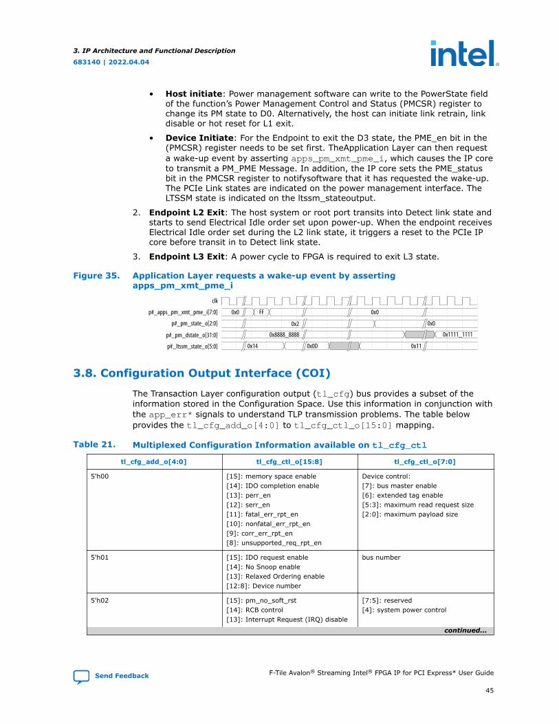
• Host initiate: Power management software can write to the PowerState fieldof the function’s Power Management Control and Status (PMCSR) register tochange its PM state to D0. Alternatively, the host can initiate link retrain, linkdisable or hot reset for L1 exit.
• Device Initiate: For the Endpoint to exit the D3 state, the PME_en bit in the(PMCSR) register needs to be set first. TheApplication Layer can then requesta wake-up event by asserting apps_pm_xmt_pme_i, which causes the IP coreto transmit a PM_PME Message. In addition, the IP core sets the PME_statusbit in the PMCSR register to notifysoftware that it has requested the wake-up.The PCIe Link states are indicated on the power management interface. TheLTSSM state is indicated on the ltssm_stateoutput.
2. Endpoint L2 Exit: The host system or root port transits into Detect link state andstarts to send Electrical Idle order set upon power-up. When the endpoint receivesElectrical Idle order set during the L2 link state, it triggers a reset to the PCIe IPcore before transit in to Detect link state.
3. Endpoint L3 Exit: A power cycle to FPGA is required to exit L3 state.
Figure 35. Application Layer requests a wake-up event by assertingapps_pm_xmt_pme_i
clk
0x0
0x14
0x2
0x1111_11110x8888_8888
0x0
0x0
FFp#_apps_pm_xmt_pme_i[7:0]
p#_Itssm_state_o[5:0]
p#_pm_dstate_o[31:0]
p#_pm_state_o[2:0]
0x0D 0x11
3.8. Configuration Output Interface (COI)
The Transaction Layer configuration output (tl_cfg) bus provides a subset of theinformation stored in the Configuration Space. Use this information in conjunction withthe app_err* signals to understand TLP transmission problems. The table belowprovides the tl_cfg_add_o[4:0] to tl_cfg_ctl_o[15:0] mapping.
Table 21. Multiplexed Configuration Information available on tl_cfg_ctl
tl_cfg_add_o[4:0] tl_cfg_ctl_o[15:8] tl_cfg_ctl_o[7:0]
5'h00 [15]: memory space enable[14]: IDO completion enable[13]: perr_en[12]: serr_en[11]: fatal_err_rpt_en[10]: nonfatal_err_rpt_en[9]: corr_err_rpt_en[8]: unsupported_req_rpt_en
Device control:[7]: bus master enable[6]: extended tag enable[5:3]: maximum read request size[2:0]: maximum payload size
5'h01 [15]: IDO request enable[14]: No Snoop enable[13]: Relaxed Ordering enable[12:8]: Device number
bus number
5'h02 [15]: pm_no_soft_rst[14]: RCB control[13]: Interrupt Request (IRQ) disable
[7:5]: reserved[4]: system power control
continued...
3. IP Architecture and Functional Description
683140 | 2022.04.04
Send Feedback F-Tile Avalon® Streaming Intel® FPGA IP for PCI Express* User Guide
45
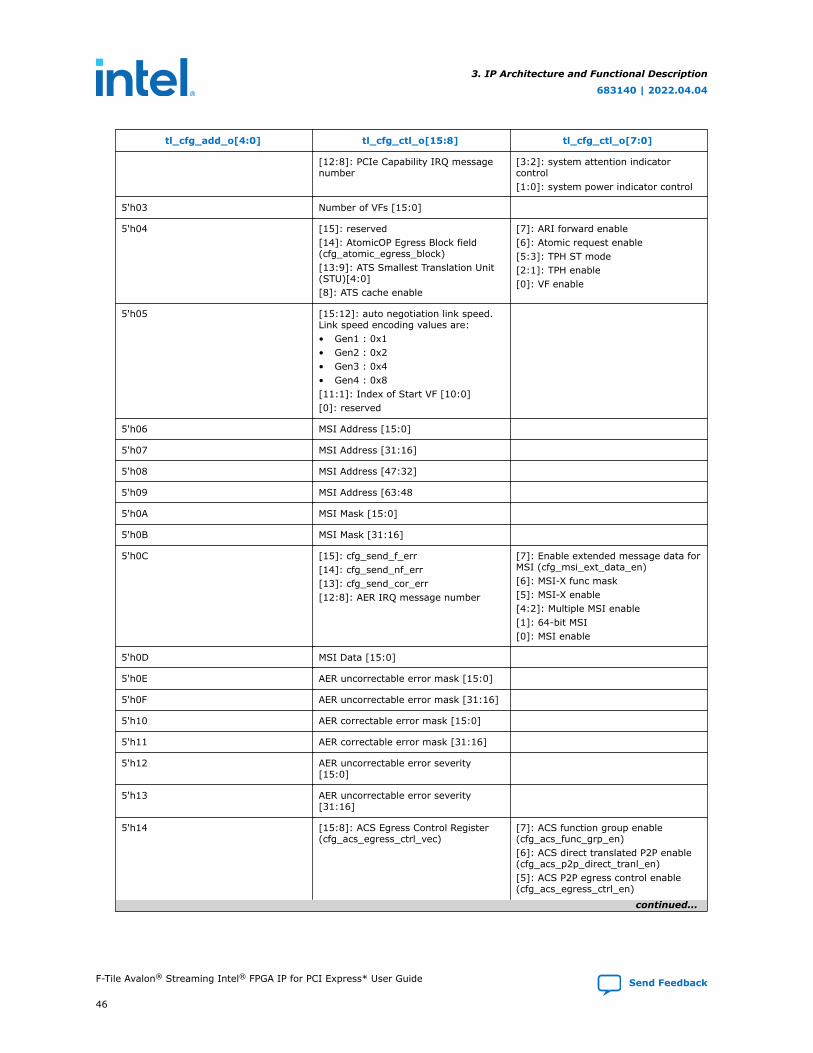
tl_cfg_add_o[4:0] tl_cfg_ctl_o[15:8] tl_cfg_ctl_o[7:0]
[12:8]: PCIe Capability IRQ messagenumber
[3:2]: system attention indicatorcontrol[1:0]: system power indicator control
5'h03 Number of VFs [15:0]
5'h04 [15]: reserved[14]: AtomicOP Egress Block field(cfg_atomic_egress_block)[13:9]: ATS Smallest Translation Unit(STU)[4:0][8]: ATS cache enable
[7]: ARI forward enable[6]: Atomic request enable[5:3]: TPH ST mode[2:1]: TPH enable[0]: VF enable
5'h05 [15:12]: auto negotiation link speed.Link speed encoding values are:• Gen1 : 0x1• Gen2 : 0x2• Gen3 : 0x4• Gen4 : 0x8[11:1]: Index of Start VF [10:0][0]: reserved
5'h06 MSI Address [15:0]
5'h07 MSI Address [31:16]
5'h08 MSI Address [47:32]
5'h09 MSI Address [63:48
5'h0A MSI Mask [15:0]
5'h0B MSI Mask [31:16]
5'h0C [15]: cfg_send_f_err[14]: cfg_send_nf_err[13]: cfg_send_cor_err[12:8]: AER IRQ message number
[7]: Enable extended message data forMSI (cfg_msi_ext_data_en)[6]: MSI-X func mask[5]: MSI-X enable[4:2]: Multiple MSI enable[1]: 64-bit MSI[0]: MSI enable
5'h0D MSI Data [15:0]
5'h0E AER uncorrectable error mask [15:0]
5'h0F AER uncorrectable error mask [31:16]
5'h10 AER correctable error mask [15:0]
5'h11 AER correctable error mask [31:16]
5'h12 AER uncorrectable error severity[15:0]
5'h13 AER uncorrectable error severity[31:16]
5'h14 [15:8]: ACS Egress Control Register(cfg_acs_egress_ctrl_vec)
[7]: ACS function group enable(cfg_acs_func_grp_en)[6]: ACS direct translated P2P enable(cfg_acs_p2p_direct_tranl_en)[5]: ACS P2P egress control enable(cfg_acs_egress_ctrl_en)
continued...
3. IP Architecture and Functional Description
683140 | 2022.04.04
F-Tile Avalon® Streaming Intel® FPGA IP for PCI Express* User Guide Send Feedback
46
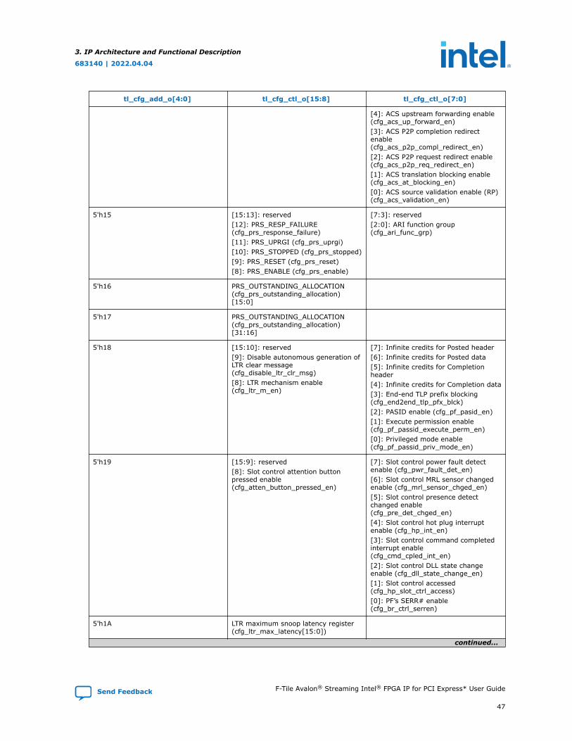
tl_cfg_add_o[4:0] tl_cfg_ctl_o[15:8] tl_cfg_ctl_o[7:0]
[4]: ACS upstream forwarding enable(cfg_acs_up_forward_en)[3]: ACS P2P completion redirectenable(cfg_acs_p2p_compl_redirect_en)[2]: ACS P2P request redirect enable(cfg_acs_p2p_req_redirect_en)[1]: ACS translation blocking enable(cfg_acs_at_blocking_en)[0]: ACS source validation enable (RP)(cfg_acs_validation_en)
5'h15 [15:13]: reserved[12]: PRS_RESP_FAILURE(cfg_prs_response_failure)[11]: PRS_UPRGI (cfg_prs_uprgi)[10]: PRS_STOPPED (cfg_prs_stopped)[9]: PRS_RESET (cfg_prs_reset)[8]: PRS_ENABLE (cfg_prs_enable)
[7:3]: reserved[2:0]: ARI function group(cfg_ari_func_grp)
5'h16 PRS_OUTSTANDING_ALLOCATION(cfg_prs_outstanding_allocation)[15:0]
5'h17 PRS_OUTSTANDING_ALLOCATION(cfg_prs_outstanding_allocation)[31:16]
5'h18 [15:10]: reserved[9]: Disable autonomous generation ofLTR clear message(cfg_disable_ltr_clr_msg)[8]: LTR mechanism enable(cfg_ltr_m_en)
[7]: Infinite credits for Posted header[6]: Infinite credits for Posted data[5]: Infinite credits for Completionheader[4]: Infinite credits for Completion data[3]: End-end TLP prefix blocking(cfg_end2end_tlp_pfx_blck)[2]: PASID enable (cfg_pf_pasid_en)[1]: Execute permission enable(cfg_pf_passid_execute_perm_en)[0]: Privileged mode enable(cfg_pf_passid_priv_mode_en)
5'h19 [15:9]: reserved[8]: Slot control attention buttonpressed enable(cfg_atten_button_pressed_en)
[7]: Slot control power fault detectenable (cfg_pwr_fault_det_en)[6]: Slot control MRL sensor changedenable (cfg_mrl_sensor_chged_en)[5]: Slot control presence detectchanged enable(cfg_pre_det_chged_en)[4]: Slot control hot plug interruptenable (cfg_hp_int_en)[3]: Slot control command completedinterrupt enable(cfg_cmd_cpled_int_en)[2]: Slot control DLL state changeenable (cfg_dll_state_change_en)[1]: Slot control accessed(cfg_hp_slot_ctrl_access)[0]: PF’s SERR# enable(cfg_br_ctrl_serren)
5'h1A LTR maximum snoop latency register(cfg_ltr_max_latency[15:0])
continued...
3. IP Architecture and Functional Description
683140 | 2022.04.04
Send Feedback F-Tile Avalon® Streaming Intel® FPGA IP for PCI Express* User Guide
47
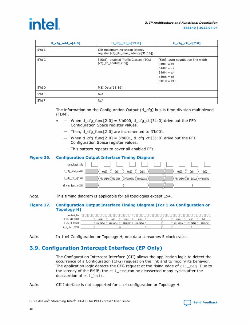
tl_cfg_add_o[4:0] tl_cfg_ctl_o[15:8] tl_cfg_ctl_o[7:0]
5'h1B LTR maximum no-snoop latencyregister (cfg_ltr_max_latency[31:16])
5'h1C [15:8]: enabled Traffic Classes (TCs)(cfg_tc_enable[7:0])
[5:0]: auto negotiation link width6’h01 = x16’h02 = x26’h04 = x46’h08 = x86’h10 = x16
5'h1D MSI Data[31:16]
5'h1E N/A
5'h1F N/A
The information on the Configuration Output (tl_cfg) bus is time-division multiplexed(TDM).
• — When tl_cfg_func[2:0] = 3'b000, tl_cfg_ctl[31:0] drive out the PF0Configuration Space register values.
— Then, tl_cfg_func[2:0] are incremented to 3'b001.
— When tl_cfg_func[2:0] = 3'b001, tl_cfg_ctl[31:0] drive out the PF1Configuration Space register values.
— This pattern repeats to cover all enabled PFs.
Figure 36. Configuration Output Interface Timing Diagram
coreclkout_hip
tl_cfg_func_o[2:0]
tl_cfg_add_o[4:0]
tl_cfg_ctl_o[15:0]
0x00 0x01 0x02 0x03 0x00 0x01 0x02
0 1
PF0 DATA0 PF0 DATA1 PF0 DATA2 PF0 DATA3 PF1 DATA0 PF1 DATA1 PF1 DATA2
Note: This timing diagram is applicable for all topologies except 1x4.
Figure 37. Configuration Output Interface Timing Diagram [For 1 x4 Configuration orTopology H]
0x00 0x01
0 1
0x02 0x03 0x00 0x01 0x2
PF0 DATA0
coreclkout_hip
tl_cfg_add_0[4:0]
tl_cfg_ctl_0[15:0]
tl_cfg_func_0[2:0]PF0 DATA1 PF0 DATA2 PF0 DATA3 PF1 DATA0 PF1 DATA1 PF1 DATA2
Note: In 1 x4 Configuration or Topology H, one data consumes 5 clock cycles.
3.9. Configuration Intercept Interface (EP Only)
The Configuration Intercept Interface (CII) allows the application logic to detect theoccurrence of a Configuration (CFG) request on the link and to modify its behavior.The application logic detects the CFG request at the rising edge of cii_req. Due tothe latency of the EMIB, the cii_req can be deasserted many cycles after thedeassertion of cii_halt.
Note: CII Interface is not supported for 1 x4 configuration or Topology H.
3. IP Architecture and Functional Description
683140 | 2022.04.04
F-Tile Avalon® Streaming Intel® FPGA IP for PCI Express* User Guide Send Feedback
48
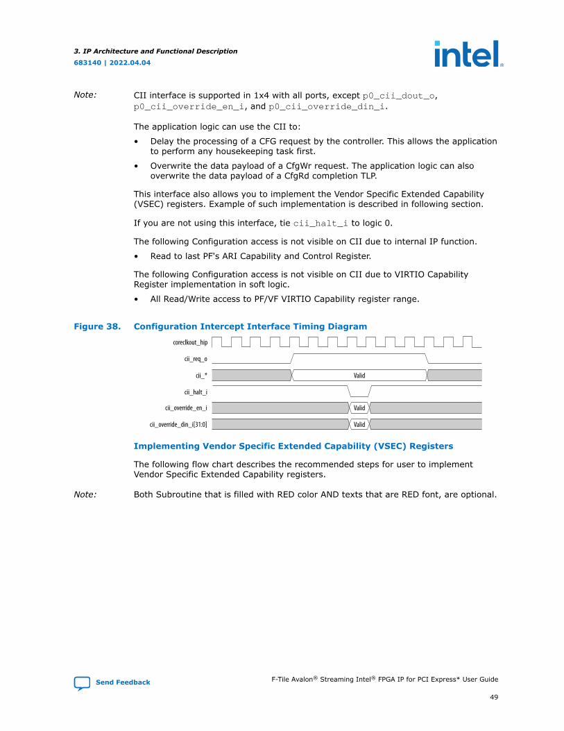
Note: CII interface is supported in 1x4 with all ports, except p0_cii_dout_o,p0_cii_override_en_i, and p0_cii_override_din_i.
The application logic can use the CII to:
• Delay the processing of a CFG request by the controller. This allows the applicationto perform any housekeeping task first.
• Overwrite the data payload of a CfgWr request. The application logic can alsooverwrite the data payload of a CfgRd completion TLP.
This interface also allows you to implement the Vendor Specific Extended Capability(VSEC) registers. Example of such implementation is described in following section.
If you are not using this interface, tie cii_halt_i to logic 0.
The following Configuration access is not visible on CII due to internal IP function.
• Read to last PF's ARI Capability and Control Register.
The following Configuration access is not visible on CII due to VIRTIO CapabilityRegister implementation in soft logic.
• All Read/Write access to PF/VF VIRTIO Capability register range.
Figure 38. Configuration Intercept Interface Timing Diagram
coreclkout_hip
cii_override_en_i
cii_override_din_i[31:0]
cii_halt_i
cii_req_o
cii_*
Valid
Valid
Valid
Implementing Vendor Specific Extended Capability (VSEC) Registers
The following flow chart describes the recommended steps for user to implementVendor Specific Extended Capability registers.
Note: Both Subroutine that is filled with RED color AND texts that are RED font, are optional.
3. IP Architecture and Functional Description
683140 | 2022.04.04
Send Feedback F-Tile Avalon® Streaming Intel® FPGA IP for PCI Express* User Guide
49
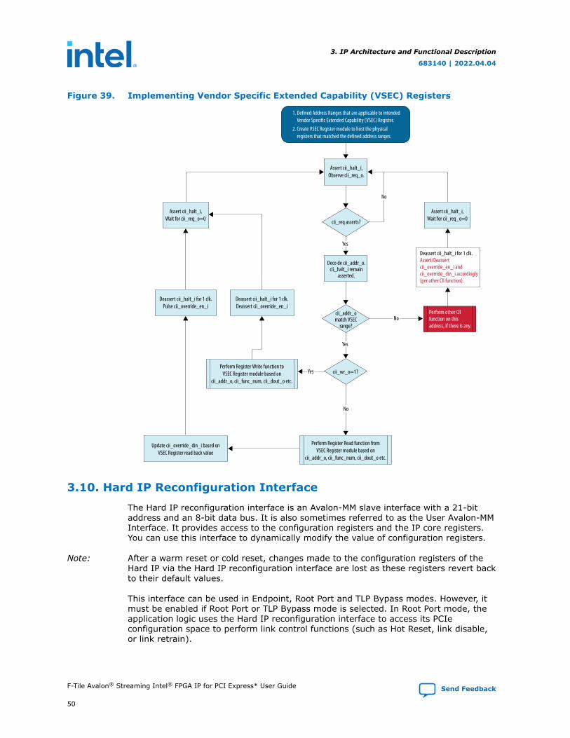
Figure 39. Implementing Vendor Specific Extended Capability (VSEC) Registers
Deassert cii_halt_i for 1 clk.Assert/Deassertcii_override_en_i andcii_override_din_i accordingly{per other CII function}.
Perform Register Write function toVSEC Register module based on
cii_addr_o, cii_func_num, cii_dout_o etc.
Perform Register Read function fromVSEC Register module based on
cii_addr_o, cii_func_num, cii_dout_o etc.
Update cii_override_din_i based onVSEC Register read back value
Yes
Yes
No
Assert cii_halt_i,Wait for cii_req_o=0
Assert cii_halt_i,Wait for cii_req_o=0
Deassert cii_halt_i for 1 clk.Pulse cii_override_en_i
Deassert cii_halt_i for 1 clk.Deassert cii_override_en_i
Deco de cii_addr_o.cii_halt_i remain
asserted.
cii_addr_omatch VSEC
range?
cii_req asserts?
cii_wr_o=1?
Assert cii_halt_i,Observe cii_req_o.
Yes
No
1. Defined Address Ranges that are applicable to intended Vendor Specific Extended Capability (VSEC) Register.2. Create VSEC Register module to host the physical registers that matched the defined address ranges.
No
Perform other CII function on this address, if there is any.
3.10. Hard IP Reconfiguration Interface
The Hard IP reconfiguration interface is an Avalon-MM slave interface with a 21-bitaddress and an 8-bit data bus. It is also sometimes referred to as the User Avalon-MMInterface. It provides access to the configuration registers and the IP core registers.You can use this interface to dynamically modify the value of configuration registers.
Note: After a warm reset or cold reset, changes made to the configuration registers of theHard IP via the Hard IP reconfiguration interface are lost as these registers revert backto their default values.
This interface can be used in Endpoint, Root Port and TLP Bypass modes. However, itmust be enabled if Root Port or TLP Bypass mode is selected. In Root Port mode, theapplication logic uses the Hard IP reconfiguration interface to access its PCIeconfiguration space to perform link control functions (such as Hot Reset, link disable,or link retrain).
3. IP Architecture and Functional Description
683140 | 2022.04.04
F-Tile Avalon® Streaming Intel® FPGA IP for PCI Express* User Guide Send Feedback
50
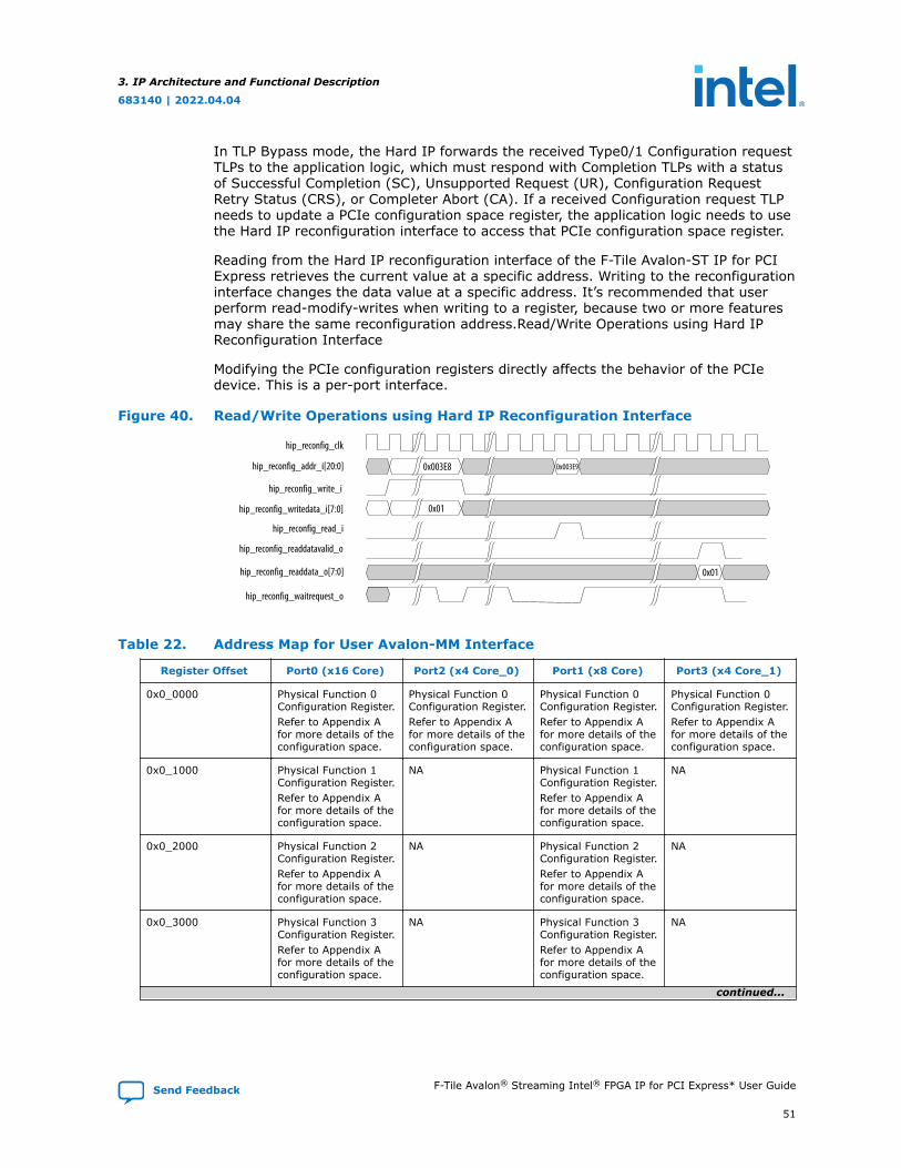
In TLP Bypass mode, the Hard IP forwards the received Type0/1 Configuration requestTLPs to the application logic, which must respond with Completion TLPs with a statusof Successful Completion (SC), Unsupported Request (UR), Configuration RequestRetry Status (CRS), or Completer Abort (CA). If a received Configuration request TLPneeds to update a PCIe configuration space register, the application logic needs to usethe Hard IP reconfiguration interface to access that PCIe configuration space register.
Reading from the Hard IP reconfiguration interface of the F-Tile Avalon-ST IP for PCIExpress retrieves the current value at a specific address. Writing to the reconfigurationinterface changes the data value at a specific address. It’s recommended that userperform read-modify-writes when writing to a register, because two or more featuresmay share the same reconfiguration address.Read/Write Operations using Hard IPReconfiguration Interface
Modifying the PCIe configuration registers directly affects the behavior of the PCIedevice. This is a per-port interface.
Figure 40. Read/Write Operations using Hard IP Reconfiguration Interface
hip_reconfig_waitrequest_o
hip_reconfig_addr_i[20:0]
hip_reconfig_write_i
hip_reconfig_clk
hip_reconfig_writedata_i[7:0]
hip_reconfig_readdatavalid_o
hip_reconfig_read_i
hip_reconfig_readdata_o[7:0]
0x003E8
0x01
0x003E9
0x01
Table 22. Address Map for User Avalon-MM Interface
Register Offset Port0 (x16 Core) Port2 (x4 Core_0) Port1 (x8 Core) Port3 (x4 Core_1)
0x0_0000 Physical Function 0Configuration Register.Refer to Appendix Afor more details of theconfiguration space.
Physical Function 0Configuration Register.Refer to Appendix Afor more details of theconfiguration space.
Physical Function 0Configuration Register.Refer to Appendix Afor more details of theconfiguration space.
Physical Function 0Configuration Register.Refer to Appendix Afor more details of theconfiguration space.
0x0_1000 Physical Function 1Configuration Register.Refer to Appendix Afor more details of theconfiguration space.
NA Physical Function 1Configuration Register.Refer to Appendix Afor more details of theconfiguration space.
NA
0x0_2000 Physical Function 2Configuration Register.Refer to Appendix Afor more details of theconfiguration space.
NA Physical Function 2Configuration Register.Refer to Appendix Afor more details of theconfiguration space.
NA
0x0_3000 Physical Function 3Configuration Register.Refer to Appendix Afor more details of theconfiguration space.
NA Physical Function 3Configuration Register.Refer to Appendix Afor more details of theconfiguration space.
NA
continued...
3. IP Architecture and Functional Description
683140 | 2022.04.04
Send Feedback F-Tile Avalon® Streaming Intel® FPGA IP for PCI Express* User Guide
51
Register Offset Port0 (x16 Core) Port2 (x4 Core_0) Port1 (x8 Core) Port3 (x4 Core_1)
0x0_4000 Physical Function 4Configuration Register.Refer to Appendix Afor more details of theconfiguration space.
NA Physical Function 4Configuration Register.Refer to Appendix Afor more details of theconfiguration space.
NA
0x0_5000 Physical Function 5Configuration Register.Refer to Appendix Afor more details of theconfiguration space.
NA Physical Function 5Configuration Register.Refer to Appendix Afor more details of theconfiguration space.
NA
0x0_6000 Physical Function 6Configuration Register.Refer to Appendix Afor more details of theconfiguration space.
NA Physical Function 6Configuration Register.Refer to Appendix Afor more details of theconfiguration space.
NA
0x0_7000 Physical Function 7Configuration Register.Refer to Appendix Afor more details of theconfiguration space.
NA Physical Function 7Configuration Register.Refer to Appendix Afor more details of theconfiguration space.
NA
0x1_4068 User Avalon-MMControl Register
User Avalon-MMControl Register
User Avalon-MMControl Register
User Avalon-MMControl Register
0x1_4200 Debug DBI Register Debug DBI Register Debug DBI Register Debug DBI Register
0x9_0000 Completion timeoutRegister
Completion timeoutRegister
Completion timeoutRegister
Completion timeoutRegister
3.10.1. Configuration Registers Access
There are two methods to access the configuration registers:
• Using direct User Avalon-MM interface (byte access)
• Using the Debug (DBI) register access (dword access). This method is useful whenyou need to read/write the entire 32 bits at one time (Counter/ Lane Margining,etc.)
3.10.1.1. Direct User Avalon-MM Interface (Byte Access)
Table 23. User Avalon-MM Control Register Bit Description
Bit Name Description Access Type Default Value
31:29 RSVD1 Reserved RO 0x0
28:18 k_vf Select the virtualfunction number
RW 0x000
17 k_vf_select To access the virtualfunction registers, thisbit should be set toone.
RW 0x0
16:2 RSVD2 Reserved RO 0x0000
1 k_shadow_select Valid only whend_vsec_select iszero.
RW 0x0
continued...
3. IP Architecture and Functional Description
683140 | 2022.04.04
F-Tile Avalon® Streaming Intel® FPGA IP for PCI Express* User Guide Send Feedback
52
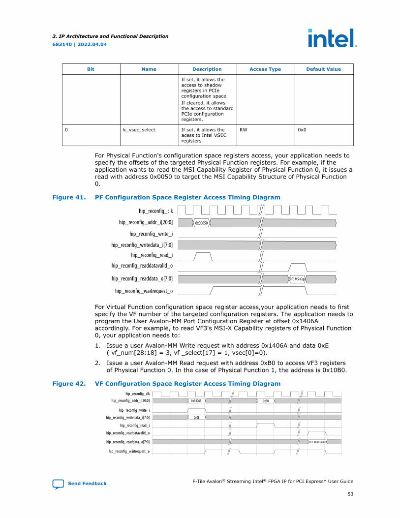
Bit Name Description Access Type Default Value
If set, it allows theaccess to shadowregisters in PCIeconfiguration space.If cleared, it allowsthe access to standardPCIe configurationregisters.
0 k_vsec_select If set, it allows theacess to Intel VSECregisters
RW 0x0
For Physical Function's configuration space registers access, your application needs tospecify the offsets of the targeted Physical Function registers. For example, if theapplication wants to read the MSI Capability Register of Physical Function 0, it issues aread with address 0x0050 to target the MSI Capability Structure of Physical Function0.
Figure 41. PF Configuration Space Register Access Timing Diagram
hip_reconfig_clk
hip_reconfig_addr_i[20:0]
hip_reconfig_write_i
hip_reconfig_writedata_i[7:0]
hip_reconfig_readdata_o[7:0]
hip_reconfig_waitrequest_o
hip_reconfig_read_i
hip_reconfig_readdatavalid_o
0x00050
PF0 MSI Cap
For Virtual Function configuration space register access,your application needs to firstspecify the VF number of the targeted configuration registers. The application needs toprogram the User Avalon-MM Port Configuration Register at offset 0x1406Aaccordingly. For example, to read VF3's MSI-X Capability registers of Physical Function0, your application needs to:
1. Issue a user Avalon-MM Write request with address 0x1406A and data 0xE( vf_num[28:18] = 3, vf _select[17] = 1, vsec[0]=0).
2. Issue a user Avalon-MM Read request with address 0xB0 to access VF3 registersof Physical Function 0. In the case of Physical Function 1, the address is 0x10B0.
Figure 42. VF Configuration Space Register Access Timing Diagramhip_reconfig_clk
hip_reconfig_addr_i[20:0]
hip_reconfig_write_i
hip_reconfig_writedata_i[7:0]
hip_reconfig_readdata_o[7:0]
hip_reconfig_waitrequest_o
hip_reconfig_read_i
hip_reconfig_readdatavalid_o
0x1406A 0xB0
VF3 MSLX Table
0x0E
3. IP Architecture and Functional Description
683140 | 2022.04.04
Send Feedback F-Tile Avalon® Streaming Intel® FPGA IP for PCI Express* User Guide
53
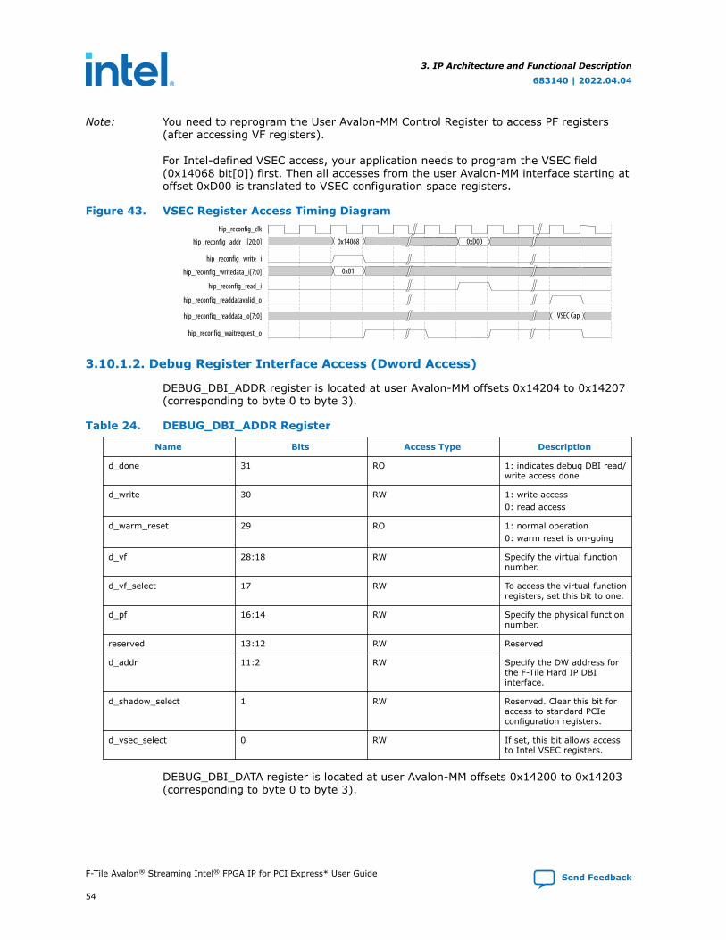
Note: You need to reprogram the User Avalon-MM Control Register to access PF registers(after accessing VF registers).
For Intel-defined VSEC access, your application needs to program the VSEC field(0x14068 bit[0]) first. Then all accesses from the user Avalon-MM interface starting atoffset 0xD00 is translated to VSEC configuration space registers.
Figure 43. VSEC Register Access Timing Diagram
0x14068 0xD00
0x01
VSEC Cap
hip_reconfig_clk
hip_reconfig_addr_i[20:0]
hip_reconfig_write_i
hip_reconfig_writedata_i[7:0]
hip_reconfig_readdata_o[7:0]
hip_reconfig_waitrequest_o
hip_reconfig_read_i
hip_reconfig_readdatavalid_o
3.10.1.2. Debug Register Interface Access (Dword Access)
DEBUG_DBI_ADDR register is located at user Avalon-MM offsets 0x14204 to 0x14207(corresponding to byte 0 to byte 3).
Table 24. DEBUG_DBI_ADDR Register
Name Bits Access Type Description
d_done 31 RO 1: indicates debug DBI read/write access done
d_write 30 RW 1: write access0: read access
d_warm_reset 29 RO 1: normal operation0: warm reset is on-going
d_vf 28:18 RW Specify the virtual functionnumber.
d_vf_select 17 RW To access the virtual functionregisters, set this bit to one.
d_pf 16:14 RW Specify the physical functionnumber.
reserved 13:12 RW Reserved
d_addr 11:2 RW Specify the DW address forthe F-Tile Hard IP DBIinterface.
d_shadow_select 1 RW Reserved. Clear this bit foraccess to standard PCIeconfiguration registers.
d_vsec_select 0 RW If set, this bit allows accessto Intel VSEC registers.
DEBUG_DBI_DATA register is located at user Avalon-MM offsets 0x14200 to 0x14203(corresponding to byte 0 to byte 3).
3. IP Architecture and Functional Description
683140 | 2022.04.04
F-Tile Avalon® Streaming Intel® FPGA IP for PCI Express* User Guide Send Feedback
54
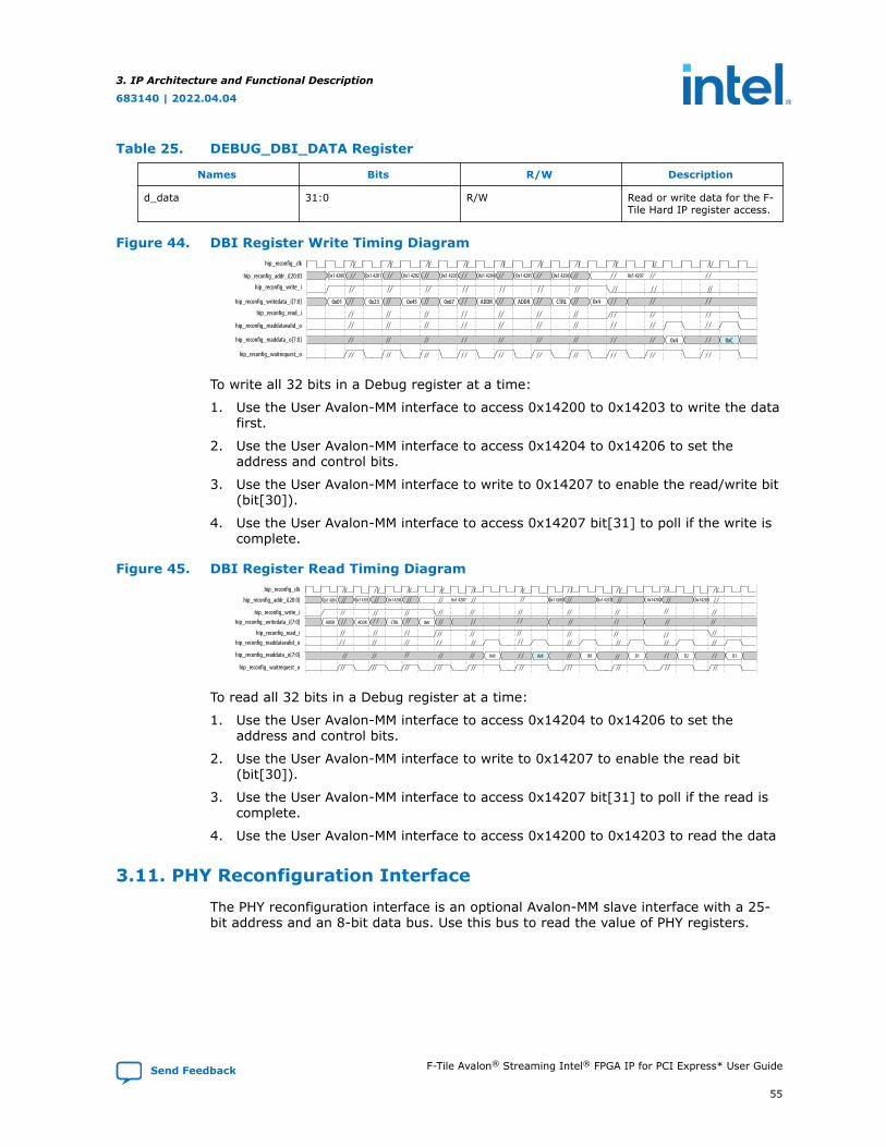
Table 25. DEBUG_DBI_DATA Register
Names Bits R/W Description
d_data 31:0 R/W Read or write data for the F-Tile Hard IP register access.
Figure 44. DBI Register Write Timing Diagramhip_reconfig_clk
hip_reconfig_addr_i[20:0]
hip_reconfig_write_i
hip_reconfig_writedata_i[7:0]
hip_reconfig_readdata_o[7:0]
hip_reconfig_waitrequest_o
hip_reconfig_read_i
hip_reconfig_readdatavalid_o
0x1 4200 0x1 4201 0x1 4202 0x1 4203 0x1 4204 0x1 4205 0x1 4206 0x1 4207
0x01 0x23 0x45 0x67 ADDR ADDR CTRL
0xC0x4
0x4
To write all 32 bits in a Debug register at a time:
1. Use the User Avalon-MM interface to access 0x14200 to 0x14203 to write the datafirst.
2. Use the User Avalon-MM interface to access 0x14204 to 0x14206 to set theaddress and control bits.
3. Use the User Avalon-MM interface to write to 0x14207 to enable the read/write bit(bit[30]).
4. Use the User Avalon-MM interface to access 0x14207 bit[31] to poll if the write iscomplete.
Figure 45. DBI Register Read Timing Diagram
0x142030x142020x1 42010x1 42000x1 42070x1 42060x1 4204 0x1 4205
CTRL 0x0ADDR ADDR
0x0 0x8 D0 D1 D2 D3
hip_reconfig_clk
hip_reconfig_addr_i[20:0]
hip_reconfig_write_ihip_reconfig_writedata_i[7:0]
hip_reconfig_readdata_o[7:0]
hip_reconfig_waitrequest_o
hip_reconfig_read_ihip_reconfig_readdatavalid_o
To read all 32 bits in a Debug register at a time:
1. Use the User Avalon-MM interface to access 0x14204 to 0x14206 to set theaddress and control bits.
2. Use the User Avalon-MM interface to write to 0x14207 to enable the read bit(bit[30]).
3. Use the User Avalon-MM interface to access 0x14207 bit[31] to poll if the read iscomplete.
4. Use the User Avalon-MM interface to access 0x14200 to 0x14203 to read the data
3.11. PHY Reconfiguration Interface
The PHY reconfiguration interface is an optional Avalon-MM slave interface with a 25-bit address and an 8-bit data bus. Use this bus to read the value of PHY registers.
3. IP Architecture and Functional Description
683140 | 2022.04.04
Send Feedback F-Tile Avalon® Streaming Intel® FPGA IP for PCI Express* User Guide
55
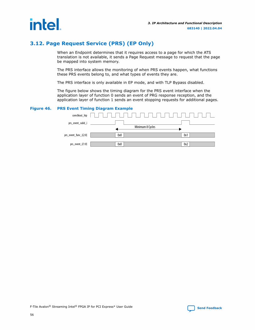
3.12. Page Request Service (PRS) (EP Only)
When an Endpoint determines that it requires access to a page for which the ATStranslation is not available, it sends a Page Request message to request that the pagebe mapped into system memory.
The PRS interface allows the monitoring of when PRS events happen, what functionsthese PRS events belong to, and what types of events they are.
The PRS interface is only available in EP mode, and with TLP Bypass disabled.
The figure below shows the timing diagram for the PRS event interface when theapplication layer of function 0 sends an event of PRG response reception, and theapplication layer of function 1 sends an event stopping requests for additional pages.
Figure 46. PRS Event Timing Diagram Example
coreclkout_hip
prs_event_valid_i
prs_event_func_i[2:0]
prs_event_i[1:0]
0x0
0x0
0x1
Minimum 8 Cycles
0x2
3. IP Architecture and Functional Description
683140 | 2022.04.04
F-Tile Avalon® Streaming Intel® FPGA IP for PCI Express* User Guide Send Feedback
56
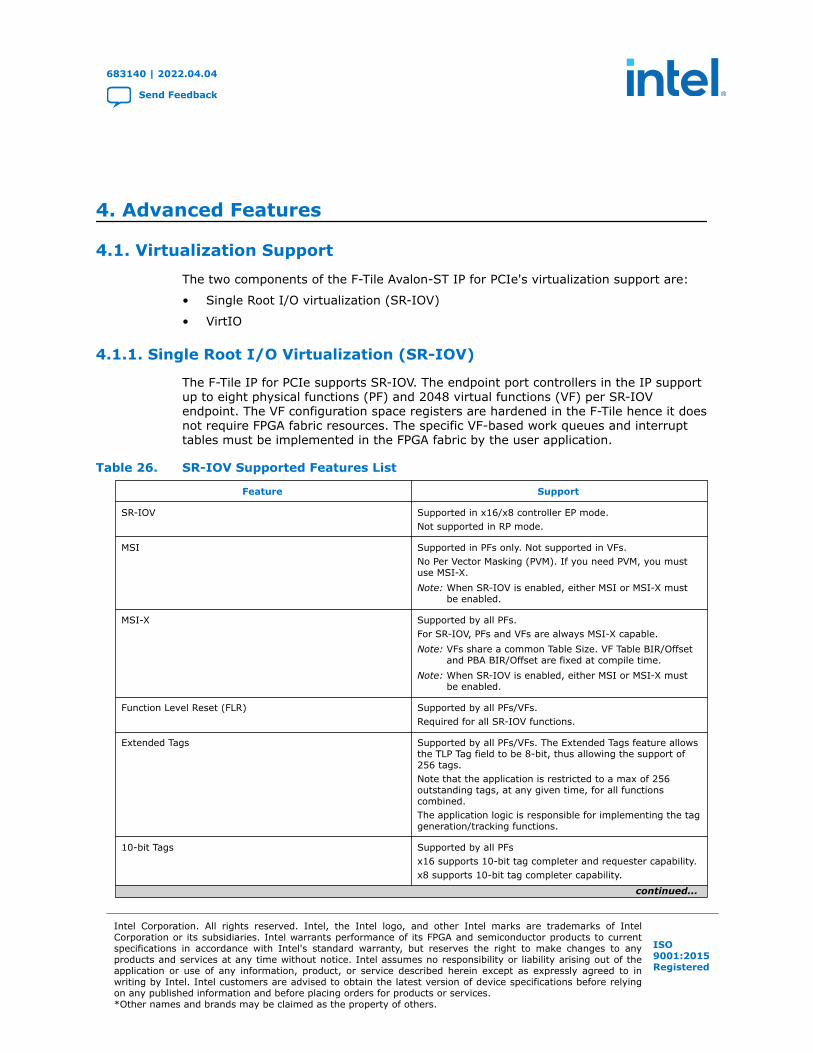
4. Advanced Features
4.1. Virtualization Support
The two components of the F-Tile Avalon-ST IP for PCIe's virtualization support are:
• Single Root I/O virtualization (SR-IOV)
• VirtIO
4.1.1. Single Root I/O Virtualization (SR-IOV)
The F-Tile IP for PCIe supports SR-IOV. The endpoint port controllers in the IP supportup to eight physical functions (PF) and 2048 virtual functions (VF) per SR-IOVendpoint. The VF configuration space registers are hardened in the F-Tile hence it doesnot require FPGA fabric resources. The specific VF-based work queues and interrupttables must be implemented in the FPGA fabric by the user application.
Table 26. SR-IOV Supported Features List
Feature Support
SR-IOV Supported in x16/x8 controller EP mode.Not supported in RP mode.
MSI Supported in PFs only. Not supported in VFs.No Per Vector Masking (PVM). If you need PVM, you mustuse MSI-X.Note: When SR-IOV is enabled, either MSI or MSI-X must
be enabled.
MSI-X Supported by all PFs.For SR-IOV, PFs and VFs are always MSI-X capable.Note: VFs share a common Table Size. VF Table BIR/Offset
and PBA BIR/Offset are fixed at compile time.Note: When SR-IOV is enabled, either MSI or MSI-X must
be enabled.
Function Level Reset (FLR) Supported by all PFs/VFs.Required for all SR-IOV functions.
Extended Tags Supported by all PFs/VFs. The Extended Tags feature allowsthe TLP Tag field to be 8-bit, thus allowing the support of256 tags.Note that the application is restricted to a max of 256outstanding tags, at any given time, for all functionscombined.The application logic is responsible for implementing the taggeneration/tracking functions.
10-bit Tags Supported by all PFsx16 supports 10-bit tag completer and requester capability.x8 supports 10-bit tag completer capability.
continued...
683140 | 2022.04.04
Send Feedback
Intel Corporation. All rights reserved. Intel, the Intel logo, and other Intel marks are trademarks of IntelCorporation or its subsidiaries. Intel warrants performance of its FPGA and semiconductor products to currentspecifications in accordance with Intel's standard warranty, but reserves the right to make changes to anyproducts and services at any time without notice. Intel assumes no responsibility or liability arising out of theapplication or use of any information, product, or service described herein except as expressly agreed to inwriting by Intel. Intel customers are advised to obtain the latest version of device specifications before relyingon any published information and before placing orders for products or services.*Other names and brands may be claimed as the property of others.
ISO9001:2015Registered
Feature Support
AER PFs are always AER capable. No AER implemented for VFs.
Active-State Power Management (ASPM) OptionalityCompliance
Supported by all PFs/VFs.Only used to indicate ASPM is not supported.
Atomic Ops Requester capability is supported by all PFs/VFs.Completer capability is supported.Compare and Swap (CAS) AtomicOps are also supported.They can handle up to 128-bit operands.
Internal Error Reporting Supported by all PFs (because all PFs are AER capable). Nosupport for VFs (because VFs do not support AER).
TLP Processing Hints 2-bit Processing Hint and 8-bit Steering Tag are supportedby all PFs/VFs. TPH Prefixes are not supported.You can optionally choose to enable the TPH Requestorcapability. However, the IP is always TPH Completercapable.
ID-Based ordering Supported by all PFs/VFs.However, the IP core does NOT perform the reordering. TheApplication Layer must do this.The IP core only provides the IDO Request & CompletionEnable bits in the Device Control 2 register. This gives theapplication permission to set the Attr bits in Requests andCompletions that it transmits.Note: Reordering capability on the RX side may be limited
by your bypass queue. On the TX side, the IP coredoes not set the IDO bits on internally generatedTLPs.
Relaxed Ordering Implemented on the RX side. This feature is always active.On the TX side, reordering is done by the application.
Alternative Routing ID Interpretation (ARI) EP (PFs/VFs) is always ARI capable. This is a device-leveloption (all lanes or none will support ARI).In addition, RP will always be ARI capable (ARI ForwardingSupported bit is always 1).
Address Translation Service (ATS) Supported by all EP PFs/VFs.
Page Request Service Interface (PRI) Supported by all EP PFs/VFs.
User Extensions (Customer VSEC) Supported by all PFs/VFs.
Gen3 Receiver Impedance (3.0 ECN) Supported
Device Serial Number Supported
Completion Timeout Ranges (Device Capabilities 2) All ranges are supported.
Data Link Layer Active Reporting Capability (LinkCapabilities)
This capability is always supported in RP mode, but not inEP mode.
Surprise Down Error Reporting Capability (Link Capabilities) Supported
PM-PCI Power Management Only D0/D3 states are supported.
ASPM (L0s/L1) Not supported
Process Address Space ID (PASID) Supported
TLP prefix Supported, mainly for PASID
Latency Tolerance Reporting (LTR) Supported (only for PASID)
Access Control Services Supported
4. Advanced Features
683140 | 2022.04.04
F-Tile Avalon® Streaming Intel® FPGA IP for PCI Express* User Guide Send Feedback
58
4.1.1.1. SR-IOV Implementation
Accessing VF PCIe Information
The PCIe configuration space for VFs is not directly available to the user application.User application can use the following methods to retrieve necessary information (busmaster enable, MSI-X etc.):
• Monitor specific VF registers using the Configuration Intercept Interface
• Read/write specific VF registers using the Hard IP Reconfiguration Interface
VF IDs are calculated within F-Tile. User application has sideband signalsrx_st_vf_num_o and rx_st_vf_active_o with the TLP to identify the associatedVFs within the PFs.
BDF Asssignment
When SR-IOV is enabled, the ARI capability is always enabled.
The F-Tile IP for PCIe automatically calculates the completer/requester ID on theTransmit side. Your application needs to provide the VF and PF information in theHeader as shown below: (For x16, sn is either s0 or s1. For x8, sn is s0).
• tx_st_hdr_sn[127]: must be set to 0
• tx_st_hdr_sn[83]: tx_st_vf_active
• tx_st_hdr_sn[82:80]: tx_st_func_num[2:0]
• tx_st_hdr_sn[95:84]: tx_st_vf_num[11:0]
In the following example, VF3 of PF1 is receiving and sending a request: For theReceive TLP:
• rx_st_func_num_o = 0x1 indicating that a VF associated with PF1 is making therequest.
• rx_st_vf_num_o = 0x3
• rx_st_vf_active_o = 1 indicating that VF3 of PF1 is the active VF.
For the Transmit TLP of VF3 associated with PF1:
• tx_st_hdr_sn[83] = 0x1
• tx_st_hdr_sn[82:80] = 0x1
• tx_st_hdr_sn[95:84] = 0x3
VF Error Reporting
The VFs, with no AER support, are required to generate Non-Fatal error messages. TheIP does not generate any error message. It is up to the user application logic togenerate appropriate messages when specific error conditions occur. The F-Tile IP forPCIe makes necessary signals available to the user application logic to generate thesemessages. The Completion Timeout Interface and VF Error Flag Interface provide thenecessary information to generate Non-Fatal error messages.
4. Advanced Features
683140 | 2022.04.04
Send Feedback F-Tile Avalon® Streaming Intel® FPGA IP for PCI Express* User Guide
59
VF to PF Mapping
VF to PF mapping always starts from the lowest possible PF number. For instance, ifthe IP has 2 PFs, wherein PF0 has 64 VFs and PF1 has 16 VFs, VF1 to VF64 aremapped to PF0, and VF65 to VF80 are mapped to PF1.
Currently, the IP core only supports the following PF/VF combinations.
Table 27. Supported PF/VF Combinations
Number of PFs Number of VFs per PF(PF0/PF1/PF2/PF3/PF4/PF5/PF6/
PF7)
Total VFs
1 8 8
1 16 16
1 32 32
1 64 64
1 128 128
1 256 256
1 512 512
2 16/16 32
2 32/32 64
2 128/128 256
2 256/256 512
2 32/0 32
2 0/32 32
2 64/0 64
2 0/64 64
2 128/0 128
2 0/128 128
2 256/0 256
2 0/256 256
2 512/0 512
2 0/512 512
2 1024/0 1024
2 0/1024 1024
2 2048/0 2048
2 0/2048 2048
4 128/0/0/0 128
4 0/128/0/0 128
4 256/0/0/0 256
4 0/256/0/0 256
continued...
4. Advanced Features
683140 | 2022.04.04
F-Tile Avalon® Streaming Intel® FPGA IP for PCI Express* User Guide Send Feedback
60
Number of PFs Number of VFs per PF(PF0/PF1/PF2/PF3/PF4/PF5/PF6/
PF7)
Total VFs
4 1024/0/0/0/0 1024
4 0/1024/0/0 1024
8 256/0/0/0/0/0/0/0 256
8 0/256/0/0/0/0/0/0 256
For example, the row that shows the combination of four PFs, 256 VFs, and thenotation 256/0/0/0 in the Number of VFs per PF column indicates that all 256 VFs aremapped to PF0, while no VF is mapped to PF1, PF2 or PF3. SR-IOV permutations allowany PF to be assigned the initial VF allocation.
4.1.1.1.1. Functional Level Reset (FLR)
Use the FLR interface to reset individual SR-IOV functions. The PCIe Hard IP supportsFLR for both PFs and VFs. If the FLR is for a specific VF, the received packets for thatVF are no longer valid.
The flr_* interface signals are provided to the application interface for this purpose.When the flr_rcvd* signal is asserted, it indicates that a FLR is received for aparticular PF/VF. Application logic needs to perform its FLR routine and send thecompletion status back on the flr_completed* interface.
The Hard IP waits for the flr_completed* status to re-enable the VF. Prior to thatevent, the Hard IP will respond to transactions to the function that is reset by the FLRas follows:
• It will discard all posted requests and return Unsupported Request (UR) for non-posted requests.
• It will discard completions as Unexpected Completions (UC).
The following figure shows the timing diagram for an FLR event targeting a PF (PF2 inthis example).
Figure 47. FLR for PF
0x02
coreclkout_hip
p0_flr_rcvd_pf_o[7:0]
p0_flr_rcvd_pf_num_o[2:0]
p0_flr_rcvd_vf_num_o[10:0]
p0_flr_completed_pf_i[7:0]
p0_flr_completed_pf_num_i[2:0]
p0_flr_completed_vf_num_i[10:0]
p0_flr_completed_vf_i
p0_flr_rcvd_vf_o
0x02
Application done with PF FLR clean up0x02
The following figure shows the timing diagram for an FLR event targeting a VF.
4. Advanced Features
683140 | 2022.04.04
Send Feedback F-Tile Avalon® Streaming Intel® FPGA IP for PCI Express* User Guide
61
Figure 48. FLR for VF
coreclkout_hip
p0_flr_rcvd_pf_o[7:0]
p0_flr_rcvd_pf_num_o[2:0]
p0_flr_rcvd_vf_num_o[10:0]
p0_flr_completed_pf_i[7:0]
p0_flr_completed_pf_num_i[2:0]
p0_flr_completed_vf_num_i[10:0]
p0_flr_completed_vf_i
p0_flr_rcvd_vf_o
PF_NUM
VF_NUM
PF_NUM
VF_NUM
0x00
0x00
Application done with VF FLR clean up
4.1.2. VirtIO
VirtIO Supported Features
• VirtIO devices are implemented as PCI Express devices.
• Support 8 PFs and 2K VFs VirtIO capability structure for each EP.
• Configuration Intercept Interface in the F-Tile IP for PCIe (EP mode only) isprovided for VirtIO transport.
• Five VirtIO device configuration structures are supported:
— Common configuration
— Notifications
— ISR Status
— Device-specific configuration (optional)
— PCI configuration access
• Location of each structure is specificed using a vendor-specific PCI capabilitylocated in the PCI configuration space of the device.
• VirtIO capability structure uses little-endian format.
• All fields of the VirtIO capability structure are read-only for the driver by default.
• Supports x16 and x8 cores.
• MSI is not supported with VirtIO.
4.1.2.1. VirtIO Implementation
The VirtIO PCI configuration access capability creates an alternative access method tothe common configuration, notifications, ISR, and device-specific configurationstructure regions. This interface provides a means for the driver to access the VirtIOdevice region of Physical Functions (PFs) or Virtual Functions (VFs).
VirtIO is an industry standard for software-based virtualization that is supportednatively by Linux. In VirtIO, software implements the virtualization stack, whereas inthe case of SR-IOV, this stack is implemented mostly in hardware.
4. Advanced Features
683140 | 2022.04.04
F-Tile Avalon® Streaming Intel® FPGA IP for PCI Express* User Guide Send Feedback
62
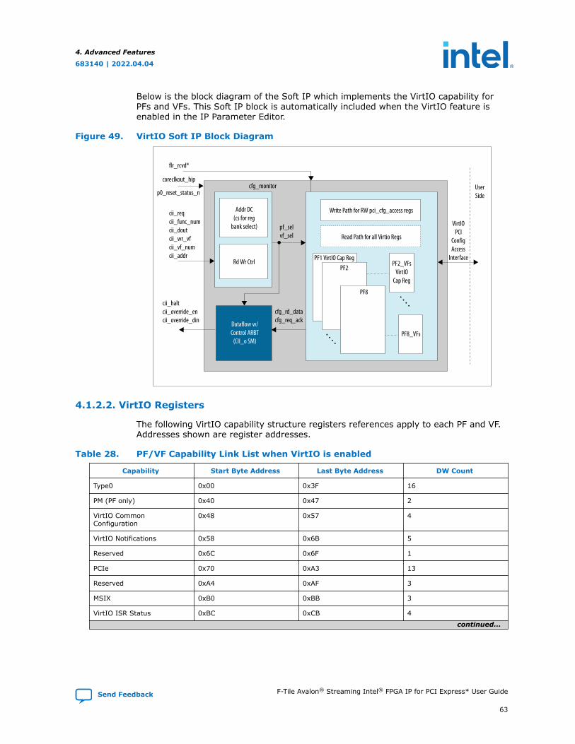
Below is the block diagram of the Soft IP which implements the VirtIO capability forPFs and VFs. This Soft IP block is automatically included when the VirtIO feature isenabled in the IP Parameter Editor.
Figure 49. VirtIO Soft IP Block Diagram
Read Path for all Virtio Regs
Write Path for RW pci_cfg_access regs
PF2PF2_VFs
VirtIOCap Reg
pf_selvf_sel
cfg_rd_datacfg_req_ackDataflow w/
Control ARBT(CII_o SM)
Addr DC(cs for reg
bank select)
cii_reqcii_func_numcii_doutcii_wr_vfcii_vf_numcii_addr
cii_haltcii_override_encii_override_din
flr_rcvd*
coreclkout_hip
p0_reset_status_n
Rd Wr Ctrl
cfg_monitor
VirtIOPCI
ConfigAccess
Interface
UserSide
PF1 VirtIO Cap Reg
PF8_VFs
PF8 • • • •
• • • •
4.1.2.2. VirtIO Registers
The following VirtIO capability structure registers references apply to each PF and VF.Addresses shown are register addresses.
Table 28. PF/VF Capability Link List when VirtIO is enabled
Capability Start Byte Address Last Byte Address DW Count
Type0 0x00 0x3F 16
PM (PF only) 0x40 0x47 2
VirtIO CommonConfiguration
0x48 0x57 4
VirtIO Notifications 0x58 0x6B 5
Reserved 0x6C 0x6F 1
PCIe 0x70 0xA3 13
Reserved 0xA4 0xAF 3
MSIX 0xB0 0xBB 3
VirtIO ISR Status 0xBC 0xCB 4
continued...
4. Advanced Features
683140 | 2022.04.04
Send Feedback F-Tile Avalon® Streaming Intel® FPGA IP for PCI Express* User Guide
63
Capability Start Byte Address Last Byte Address DW Count
VirtIO Device-SpecificConfiguration
0xCC 0xDB 4
VirtIO PCI ConfigurationAccess
0xDC 0xEF 5
Reserved 0xF0 0xFF 4
Table 29. VirtIO Capability Structures
Address Name Description
VirtIO Common Configuration Capability Structure
012 Common Configuration CapabilityRegister
Capability ID, next capability pointer,capability length
013 BAR Indicator Register Lower 8 bits indicate which BAR holdsthe structure
014 BAR Offset Register Indicates starting address of thestructure within the BAR
015 Structure Length Register Indicates length of structure
VirtIO Notifications Capability Structure
016 Notifications Capability Register Capability ID, next capability pointer,capability length
017 BAR Indicator Register Lower 8 bits indicate which BAR holdsthe structure
018 BAR Offset Register Indicates starting address of thestructure within the BAR
019 Structure Length Register Indicates length of structure
01A Notify Off Multiplier Multiplier for queue_notify_off
VirtIO ISR Status Capability Structure
02F ISR Status Capability Register Capability ID, next capability pointer,capability length
030 BAR Indicator Register Lower 8 bits indicate which BAR holdsthe structure
031 BAR Offset Register Indicates starting address of thestructure within the BAR
032 Structure Length Register Indicates length of structure
VirtIO Device-Specific Capability Structure (Optional)
033 Device Specific Capability Register Capability ID, next capability pointer,capability length
034 BAR Indicator Register Lower 8 bits indicate which BAR holdsthe structure
035 BAR Offset Register Indicates starting address of thestructure within the BAR
036 Structure Length Register Indicates length of structure
VirtIO PCI Configuration Access Structurecontinued...
4. Advanced Features
683140 | 2022.04.04
F-Tile Avalon® Streaming Intel® FPGA IP for PCI Express* User Guide Send Feedback
64
Address Name Description
037 PCI Configuration Access CapabilityRegister
Capability ID, next capability pointer,capability length
038 BAR Indicator Register Lower 8 bits indicate which BAR holdsthe structure
039 BAR Offset Register Indicates starting address of thestructure within the BAR
03A Structure Length Register Indicates length of structure
03B PCI Configuration Data Data for BAR access
Table 30. VirtIO Common Configuration Capability Register (Address: 0x012)
Bit Location Description Access Type Default Value
31:24 Configuration Type RO 0x01
23:16 Capability Length RO 0x10
15:8 Next Capability Pointer RO 0x58
7:0 Capability ID RO 0x09
Note: The capability register identifies that this is a vendor-specific capability. It alsoidentifies the structure type.
Table 31. VirtIO Common Configuration BAR Indicator Register (Address: 0x013)
Bit Location Description Access Type Default Value
31:24 Padding RO 0x00
23:16 Padding RO 0x00
15:8 Padding RO 0x00
7:0 BAR Indicator RO Programmable
Note: The Bar Indicator field holds the values 0x0 to 0x5 specifying a Base Address register(BAR) belonging to the function located beginning at 10h in PCI Configuration Space.The BAR is used to map the structure into the memory space. Any other value isreserved for future use.
Table 32. VirtIO Common Configuration BAR Offset Register (Address: 0x014)
Bit Location Description Access Type Default Value
31:0 BAR Offset RO Programmable
Note: This register indicates where the structure begins relative to the base addressassociated with the BAR. The alignment requirements of the offset are indicated ineach structure-specific section.
Table 33. VirtIO Common Configuration Structure Length Register (Address: 0x015)
Bit Location Description Access Type Default Value
31:0 Structure Length RO Programmable
4. Advanced Features
683140 | 2022.04.04
Send Feedback F-Tile Avalon® Streaming Intel® FPGA IP for PCI Express* User Guide
65
Note: The capability register identifies that this is a vendor-specific capability. It alsoidentifies the structure type.
Table 34. VirtIO Notifications Capability Register (Address: 0x016)
Bit Location Description Access Type Default Value
31:24 Configuration Type RO 0x02
23:16 Capability Length RO 0x14
15:8 Next Capability Pointer RO 0xBC
7:0 Capability ID RO 0x09
Note: The capability register identifies that this is a vendor-specific capability. It alsoidentifies the structure type.
Table 35. VirtIO Notifications BAR Indicator Register (Address: 0x017)
Bit Location Description Access Type Default Value
31:24 Padding RO 0x00
23:16 Padding RO 0x00
15:8 Padding RO 0x00
7:0 BAR Indicator RO Programmable
Note: The Bar Indicator field holds the values 0x0 to 0x5 specifying a Base Address register(BAR) belonging to the function located beginning at 10h in PCI Configuration Space.The BAR is used to map the structure into memory space. Any other value is reservedfor future use.
Table 36. VirtIO Notifications BAR Offset Register (Address: 0x018)
Bit Location Description Access Type Default Value
31:0 BAR Offset RO 31:0
Note: This register indicates where the structure begins relative to the base addressassociated with the BAR. The alignment requirements of the offset are indicated ineach structure-specific section.
Table 37. VirtIO Notifications Structure Length Register (Address: 0x019)
Bit Location Description Access Type Default Value
31:0 Structure Length RO 31:0
Note: The length register indicates the length of the structure. The length may includepadding, fields unused by the driver, or future extensions.
Table 38. VirtIO Notifications Notify Off Multiplier Register (Address: 0x01A)
Bit Location Description Access Type Default Value
31:0 Multiplier forqueue_notify_off
RO 31:0
4. Advanced Features
683140 | 2022.04.04
F-Tile Avalon® Streaming Intel® FPGA IP for PCI Express* User Guide Send Feedback
66
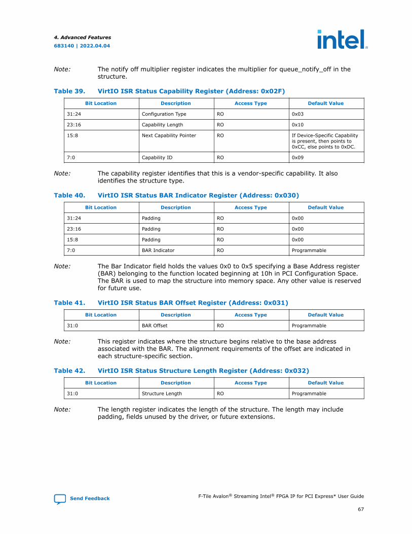
Note: The notify off multiplier register indicates the multiplier for queue_notify_off in thestructure.
Table 39. VirtIO ISR Status Capability Register (Address: 0x02F)
Bit Location Description Access Type Default Value
31:24 Configuration Type RO 0x03
23:16 Capability Length RO 0x10
15:8 Next Capability Pointer RO If Device-Specific Capabilityis present, then points to0xCC, else points to 0xDC.
7:0 Capability ID RO 0x09
Note: The capability register identifies that this is a vendor-specific capability. It alsoidentifies the structure type.
Table 40. VirtIO ISR Status BAR Indicator Register (Address: 0x030)
Bit Location Description Access Type Default Value
31:24 Padding RO 0x00
23:16 Padding RO 0x00
15:8 Padding RO 0x00
7:0 BAR Indicator RO Programmable
Note: The Bar Indicator field holds the values 0x0 to 0x5 specifying a Base Address register(BAR) belonging to the function located beginning at 10h in PCI Configuration Space.The BAR is used to map the structure into memory space. Any other value is reservedfor future use.
Table 41. VirtIO ISR Status BAR Offset Register (Address: 0x031)
Bit Location Description Access Type Default Value
31:0 BAR Offset RO Programmable
Note: This register indicates where the structure begins relative to the base addressassociated with the BAR. The alignment requirements of the offset are indicated ineach structure-specific section.
Table 42. VirtIO ISR Status Structure Length Register (Address: 0x032)
Bit Location Description Access Type Default Value
31:0 Structure Length RO Programmable
Note: The length register indicates the length of the structure. The length may includepadding, fields unused by the driver, or future extensions.
4. Advanced Features
683140 | 2022.04.04
Send Feedback F-Tile Avalon® Streaming Intel® FPGA IP for PCI Express* User Guide
67
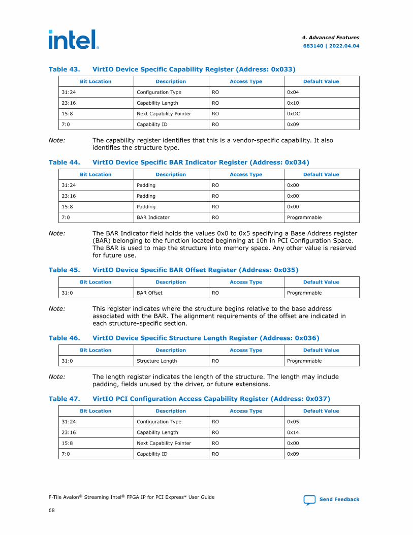
Table 43. VirtIO Device Specific Capability Register (Address: 0x033)
Bit Location Description Access Type Default Value
31:24 Configuration Type RO 0x04
23:16 Capability Length RO 0x10
15:8 Next Capability Pointer RO 0xDC
7:0 Capability ID RO 0x09
Note: The capability register identifies that this is a vendor-specific capability. It alsoidentifies the structure type.
Table 44. VirtIO Device Specific BAR Indicator Register (Address: 0x034)
Bit Location Description Access Type Default Value
31:24 Padding RO 0x00
23:16 Padding RO 0x00
15:8 Padding RO 0x00
7:0 BAR Indicator RO Programmable
Note: The BAR Indicator field holds the values 0x0 to 0x5 specifying a Base Address register(BAR) belonging to the function located beginning at 10h in PCI Configuration Space.The BAR is used to map the structure into memory space. Any other value is reservedfor future use.
Table 45. VirtIO Device Specific BAR Offset Register (Address: 0x035)
Bit Location Description Access Type Default Value
31:0 BAR Offset RO Programmable
Note: This register indicates where the structure begins relative to the base addressassociated with the BAR. The alignment requirements of the offset are indicated ineach structure-specific section.
Table 46. VirtIO Device Specific Structure Length Register (Address: 0x036)
Bit Location Description Access Type Default Value
31:0 Structure Length RO Programmable
Note: The length register indicates the length of the structure. The length may includepadding, fields unused by the driver, or future extensions.
Table 47. VirtIO PCI Configuration Access Capability Register (Address: 0x037)
Bit Location Description Access Type Default Value
31:24 Configuration Type RO 0x05
23:16 Capability Length RO 0x14
15:8 Next Capability Pointer RO 0x00
7:0 Capability ID RO 0x09
4. Advanced Features
683140 | 2022.04.04
F-Tile Avalon® Streaming Intel® FPGA IP for PCI Express* User Guide Send Feedback
68
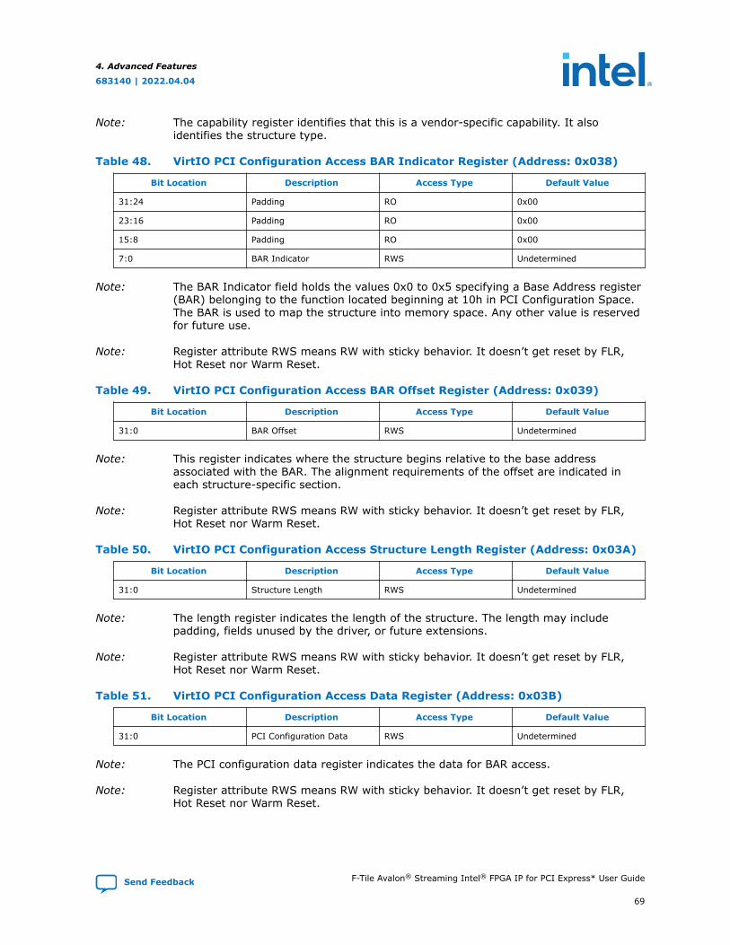
Note: The capability register identifies that this is a vendor-specific capability. It alsoidentifies the structure type.
Table 48. VirtIO PCI Configuration Access BAR Indicator Register (Address: 0x038)
Bit Location Description Access Type Default Value
31:24 Padding RO 0x00
23:16 Padding RO 0x00
15:8 Padding RO 0x00
7:0 BAR Indicator RWS Undetermined
Note: The BAR Indicator field holds the values 0x0 to 0x5 specifying a Base Address register(BAR) belonging to the function located beginning at 10h in PCI Configuration Space.The BAR is used to map the structure into memory space. Any other value is reservedfor future use.
Note: Register attribute RWS means RW with sticky behavior. It doesn’t get reset by FLR,Hot Reset nor Warm Reset.
Table 49. VirtIO PCI Configuration Access BAR Offset Register (Address: 0x039)
Bit Location Description Access Type Default Value
31:0 BAR Offset RWS Undetermined
Note: This register indicates where the structure begins relative to the base addressassociated with the BAR. The alignment requirements of the offset are indicated ineach structure-specific section.
Note: Register attribute RWS means RW with sticky behavior. It doesn’t get reset by FLR,Hot Reset nor Warm Reset.
Table 50. VirtIO PCI Configuration Access Structure Length Register (Address: 0x03A)
Bit Location Description Access Type Default Value
31:0 Structure Length RWS Undetermined
Note: The length register indicates the length of the structure. The length may includepadding, fields unused by the driver, or future extensions.
Note: Register attribute RWS means RW with sticky behavior. It doesn’t get reset by FLR,Hot Reset nor Warm Reset.
Table 51. VirtIO PCI Configuration Access Data Register (Address: 0x03B)
Bit Location Description Access Type Default Value
31:0 PCI Configuration Data RWS Undetermined
Note: The PCI configuration data register indicates the data for BAR access.
Note: Register attribute RWS means RW with sticky behavior. It doesn’t get reset by FLR,Hot Reset nor Warm Reset.
4. Advanced Features
683140 | 2022.04.04
Send Feedback F-Tile Avalon® Streaming Intel® FPGA IP for PCI Express* User Guide
69
4.2. TLP Bypass Mode
The F-Tile Avalon-ST IP for PCIe includes a TLP Bypass mode for both downstream andupstream ports to allow the implementation of advanced features such as:
• The upstream port or the downstream port of a switch.
• A custom implementation of a Transaction Layer to meet specific userrequirements.
Table 52. Supported TLP Bypass ConfigurationsUP=Upstream Port ; DN=Downstream Port
IP Mode Port Mode
1x16 UPDN
2x8 UP/UPUP/DNEP/UPDN/DN
4x4 UP/UP/UP/UPDN/DN/DN/DN
The F-Tile Avalon-ST IP IP in TLP Bypass mode still includes some of the PCIeconfiguration space registers related to link operation.
F-Tile Avalon-ST IP interfaces with the application logic via the Avalon-ST interface (forall TLP traffic), the User Avalon-MM interface (via Hard IP Reconfiguration interface,for Lite TL’s configuration registers access) and other miscellaneous signals.
In TLP bypass mode, F-Tile supports the autonomous Hard IP feature. It responds toconfiguration accesses before the FPGA fabric enters user mode with Completions witha CRS code. However, in TLP bypass mode, CvP init and update are not supported.
When the TLP Bypass feature is enabled, the F-Tile Avalon-ST IP does not processreceived TLPs internally but outputs them to the user application. This allows theapplication to implement a custom Transaction Layer.
Note: In TLP Bypass mode, the PCIe Hard IP does not generate/check the ECRC and will notremove it if the received TLP has the ECRC.
4. Advanced Features
683140 | 2022.04.04
F-Tile Avalon® Streaming Intel® FPGA IP for PCI Express* User Guide Send Feedback
70
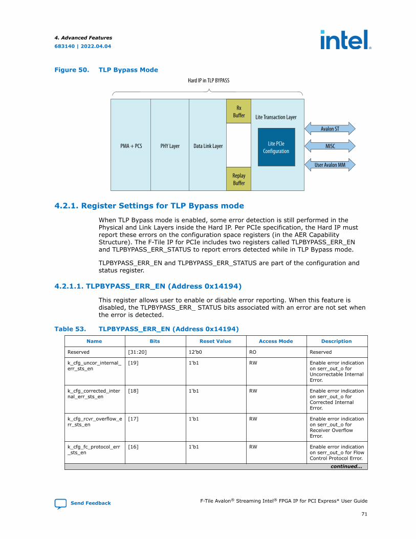
Figure 50. TLP Bypass Mode
Lite PCIeConfiguration
Lite Transaction Layer
Data Link Layer
Hard IP in TLP BYPASS
PHY LayerPMA + PCS MISC
User Avalon MM
ReplayBuffer
RxBuffer
Avalon ST
4.2.1. Register Settings for TLP Bypass mode
When TLP Bypass mode is enabled, some error detection is still performed in thePhysical and Link Layers inside the Hard IP. Per PCIe specification, the Hard IP mustreport these errors on the configuration space registers (in the AER CapabilityStructure). The F-Tile IP for PCIe includes two registers called TLPBYPASS_ERR_ENand TLPBYPASS_ERR_STATUS to report errors detected while in TLP Bypass mode.
TLPBYPASS_ERR_EN and TLPBYPASS_ERR_STATUS are part of the configuration andstatus register.
4.2.1.1. TLPBYPASS_ERR_EN (Address 0x14194)
This register allows user to enable or disable error reporting. When this feature isdisabled, the TLPBYPASS_ERR_ STATUS bits associated with an error are not set whenthe error is detected.
Table 53. TLPBYPASS_ERR_EN (Address 0x14194)
Name Bits Reset Value Access Mode Description
Reserved [31:20] 12’b0 RO Reserved
k_cfg_uncor_internal_err_sts_en
[19] 1'b1 RW Enable error indicationon serr_out_o forUncorrectable InternalError.
k_cfg_corrected_internal_err_sts_en
[18] 1'b1 RW Enable error indicationon serr_out_o forCorrected InternalError.
k_cfg_rcvr_overflow_err_sts_en
[17] 1'b1 RW Enable error indicationon serr_out_o forReceiver OverflowError.
k_cfg_fc_protocol_err_sts_en
[16] 1'b1 RW Enable error indicationon serr_out_o for FlowControl Protocol Error.
continued...
4. Advanced Features
683140 | 2022.04.04
Send Feedback F-Tile Avalon® Streaming Intel® FPGA IP for PCI Express* User Guide
71
Name Bits Reset Value Access Mode Description
k_cfg_mlf_tlp_err_sts_en
[15] 1'b1 RW Enable error indicationon serr_out_o forMalformed TLP Error.
k_cfg_surprise_down_err_sts_en
[14] 1'b1 RW Enable error indicationon serr_out_o forSurprise Down Error.
k_cfg_dl_protocol_err_sts_en
[13] 1'b1 RW Enable error indicationon serr_out_o forData Link ProtocolError.
k_cfg_replay_number_rollover_err_sts_en
[12] 1'b1 RW Enable error indicationon serr_out_o forREPLAY_NUM RolloverError.
k_cfg_replay_timer_timeout_err_st_en
[11] 1'b1 RW Enable error indicationon serr_out_o forReplay Timer TimeoutError.
k_cfg_bad_dllp_err_sts_en
[10] 1'b1 RW Enable error indicationon serr_out_o for BadDLLP Error.
k_cfg_bad_tlp_err_sts_en
[9] 1'b1 RW Enable error indicationon serr_out_o for BadTLP Error.
k_cfg_rcvr_err_sts_en [8] 1'b1 RW Enable error indicationon serr_out_o forReceiver Error.
Reserved [7:1] 7'b0 RO Reserved
k_cfg_ecrc_err_sts_en [0] 1'b1 RW Enable error indicationon serr_out_o forECRC Error.
4.2.1.2. TLPBYPASS_ERR_STATUS (Address 0x14190)
When an error is detected, it is recommended that user reads the PF0 AER registerinside F-Tile to get detailed information about the error. To clear the previous errorstatus, user needs to clear TLPBYPASS_ERR_STATUS and the correspondingcorrectable and uncorrectable error status registers in the AER capability structure.After doing that, user can get the new error update from this register.
This register allows user to enable or disable error reporting. When this feature isdisabled, the TLPBYPASS_ERR_ STATUS bits associated with an error are not set whenthe error is detected.
Table 54. TLPBYPASS_ERR_EN (Address 0x14194)
Name Bits Reset Value Access Mode Description
Reserved [31:20] 12’b0 RO Reserved
cfg_uncor_internal_err_sts
[19] 1'b0 W1C Uncorrectable InternalError
cfg_corrected_internal_err_sts
[18] 1'b0 W1C Corrected InternalError
continued...
4. Advanced Features
683140 | 2022.04.04
F-Tile Avalon® Streaming Intel® FPGA IP for PCI Express* User Guide Send Feedback
72
Name Bits Reset Value Access Mode Description
cfg_rcvr_overflow_err_sts
[17] 1'b0 W1C Receiver OverflowError
cfg_fc_protocol_err_sts
[16] 1'b0 W1C Flow Control ProtocolError
cfg_mlf_tlp_err_sts [15] 1'b0 W1C Malformed TLP Error
cfg_surprise_down_err_sts
[14] 1'b0 W1C Surprise Down Error.Available indownstream modeonly.
cfg_dl_protocol_err_sts
[13] 1'b0 W1C Data Link ProtocolError
cfg_replay_number_rollover_err_sts
[12] 1'b0 W1C REPLAY_NUM RolloverError
cfg_replay_timer_timeout_err_sts
[11] 1'b0 W1C Replay Timer TimeoutError
cfg_bad_dllp_err_sts [10] 1'b0 W1C Bad DLLP Error
cfg_bad_tlp_err_sts [9] 1'b0 W1C Bad TLP Error
cfg_rcvr_err_sts [8] 1'b0 W1C Receiver Error
Reserved [7:1] 7'b0 RO Reserved
cfg_ecrc_err_sts [0] 1'b0 W1C ECRC Error
4.2.2. Avalon-MM usage for TLP Bypass Mode
The majority of the PCIe standard registers are implemented in the user’s logicoutside of the F-Tile Avalon-ST IP. However, the following registers still remain insidethe F-Tile:
• Power management capability
• PCI Express capability
• Secondary PCI Express capability
• Data link feature extended capability
• Physical layer 16.0GT/s extended capability
• Lane margining at the receiver extended capability
• Advanced error reporting capability
The application can only access PCIe controller registers through the User Avalon-MM/Hard IP Reconfiguration interface. For more details on the signals in this interface,refer to the Hard IP Reconfiguration Interface on page 110.
There are two options to implement Device ID and Vendor ID of the PCIeConfiguration Header Registers.
1. Specify the Device ID and Vendor ID in the IP Parameter Editor and then readthem from the PCIe Controller through the User Avalon-MM interface.
2. Implement the Device ID and Vendor ID in the user logic. The rest of the registersof PCIe Configuration Header Registers must be implemented in the user logic.
4. Advanced Features
683140 | 2022.04.04
Send Feedback F-Tile Avalon® Streaming Intel® FPGA IP for PCI Express* User Guide
73
Table 55. Capability Registers to be Updated by the Application Logic via the UserAvalon-MM Interface
Capability Comments
Power Management Capability Need to write back since it is required to trigger a PCI-PMentry.
PCI Express Capability All the PCIe capabilities, control and status registers are forconfiguring the device. Write-back is required.
Secondary PCI Express Capability Secondary PCIe Capability is required for configuring thedevice.
Data Link Feature Extended Capability Data Link Capability is device specific.
Physical Layer 16.0 GT/s Extended Capability Physical Layer 16G Capability is device specific.
Lane Margining at the Receiver Extended Capability Margining Extended Capability is device specific.
Advanced Error Reporting Capability Write-back to error status registers is required for TLPBypass.
4.2.3. Transmit Interface
All TLPs transmitted by the application through the TX streaming interface are sent outas-is, without any tracking for completion. The F-Tile AVST IP for PCIe does notperform any check on the TLPs. User application logic is responsible for sending TLPsthat comply with the PCIe specifications.
4.2.4. Receive Interface
ALL TLPs received by the IP are transmitted to the application through the RXstreaming interface (except Malformed TLPs). All PCIe protocol errors leading up todesignating a TLP packet as a good packet or not will be detected by the Hard IP andcommunicated to user logic to take appropriate action in terms of error logging andescalation. The IP does not generate any error message internally, since this is theresponsibility of the user logic. Please refer to the Packets Forwarded to the UserApplication in TLP Bypass Mode Appendix C for detailed information.
4.2.5. Configuration TLP
The F-Tile AVST IP forwards any received Type0/1 Configuration TLP to the Avalon-STRX streaming interface. User logic has the responsibility to respond with a CompletionTLP with a Completion code of Successful Completion (SC), Unsupported Request(UR), Configuration Request Retry Status (CRS), or Completer Abort (CA).
If a Configuration TLP needs to update a register in the PCIe configuration space in theF-Tile PCIe Hard IP, you need to use the User Avalon-MM/Hard IP Reconfigurationinterface. The application needs to prevent link programming side effects such aswriting into low-power states before sending the Completion associated with therequest.
The application logic can check the TX FIFO empty flag in the tx_cdts_limit_oafter the Completion enters the TX streaming interface to confirm that the TLP hasbeen sent. For more information on the User Avalon-MM interface, refer to Hard IPReconfiguration Interface on page 110.
4. Advanced Features
683140 | 2022.04.04
F-Tile Avalon® Streaming Intel® FPGA IP for PCI Express* User Guide Send Feedback
74
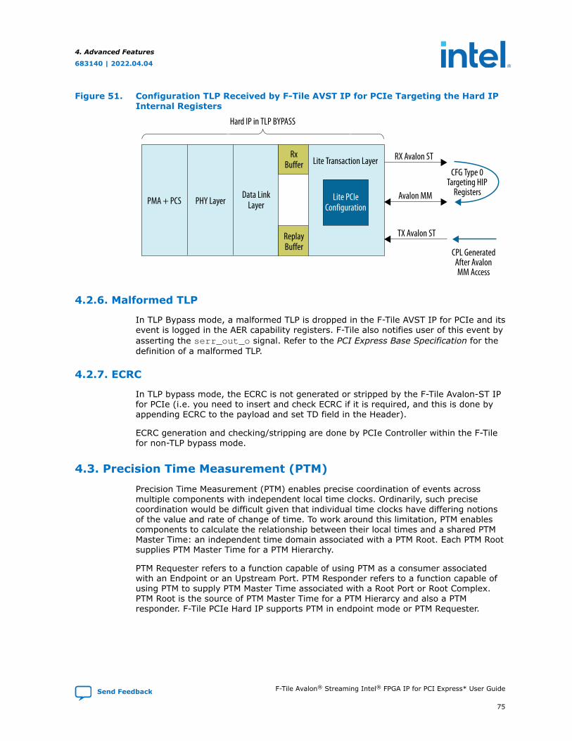
Figure 51. Configuration TLP Received by F-Tile AVST IP for PCIe Targeting the Hard IPInternal Registers
PMA + PCS PHY Layer
Hard IP in TLP BYPASS
Data LinkLayer
RxBuffer
ReplayBuffer
Lite Transaction Layer RX Avalon ST
TX Avalon ST
Avalon MM
CPL GeneratedAfter AvalonMM Access
CFG Type 0Targeting HIP
RegistersLite PCIeConfiguration
4.2.6. Malformed TLP
In TLP Bypass mode, a malformed TLP is dropped in the F-Tile AVST IP for PCIe and itsevent is logged in the AER capability registers. F-Tile also notifies user of this event byasserting the serr_out_o signal. Refer to the PCI Express Base Specification for thedefinition of a malformed TLP.
4.2.7. ECRC
In TLP bypass mode, the ECRC is not generated or stripped by the F-Tile Avalon-ST IPfor PCIe (i.e. you need to insert and check ECRC if it is required, and this is done byappending ECRC to the payload and set TD field in the Header).
ECRC generation and checking/stripping are done by PCIe Controller within the F-Tilefor non-TLP bypass mode.
4.3. Precision Time Measurement (PTM)
Precision Time Measurement (PTM) enables precise coordination of events acrossmultiple components with independent local time clocks. Ordinarily, such precisecoordination would be difficult given that individual time clocks have differing notionsof the value and rate of change of time. To work around this limitation, PTM enablescomponents to calculate the relationship between their local times and a shared PTMMaster Time: an independent time domain associated with a PTM Root. Each PTM Rootsupplies PTM Master Time for a PTM Hierarchy.
PTM Requester refers to a function capable of using PTM as a consumer associatedwith an Endpoint or an Upstream Port. PTM Responder refers to a function capable ofusing PTM to supply PTM Master Time associated with a Root Port or Root Complex.PTM Root is the source of PTM Master Time for a PTM Hierarcy and also a PTMresponder. F-Tile PCIe Hard IP supports PTM in endpoint mode or PTM Requester.
4. Advanced Features
683140 | 2022.04.04
Send Feedback F-Tile Avalon® Streaming Intel® FPGA IP for PCI Express* User Guide
75
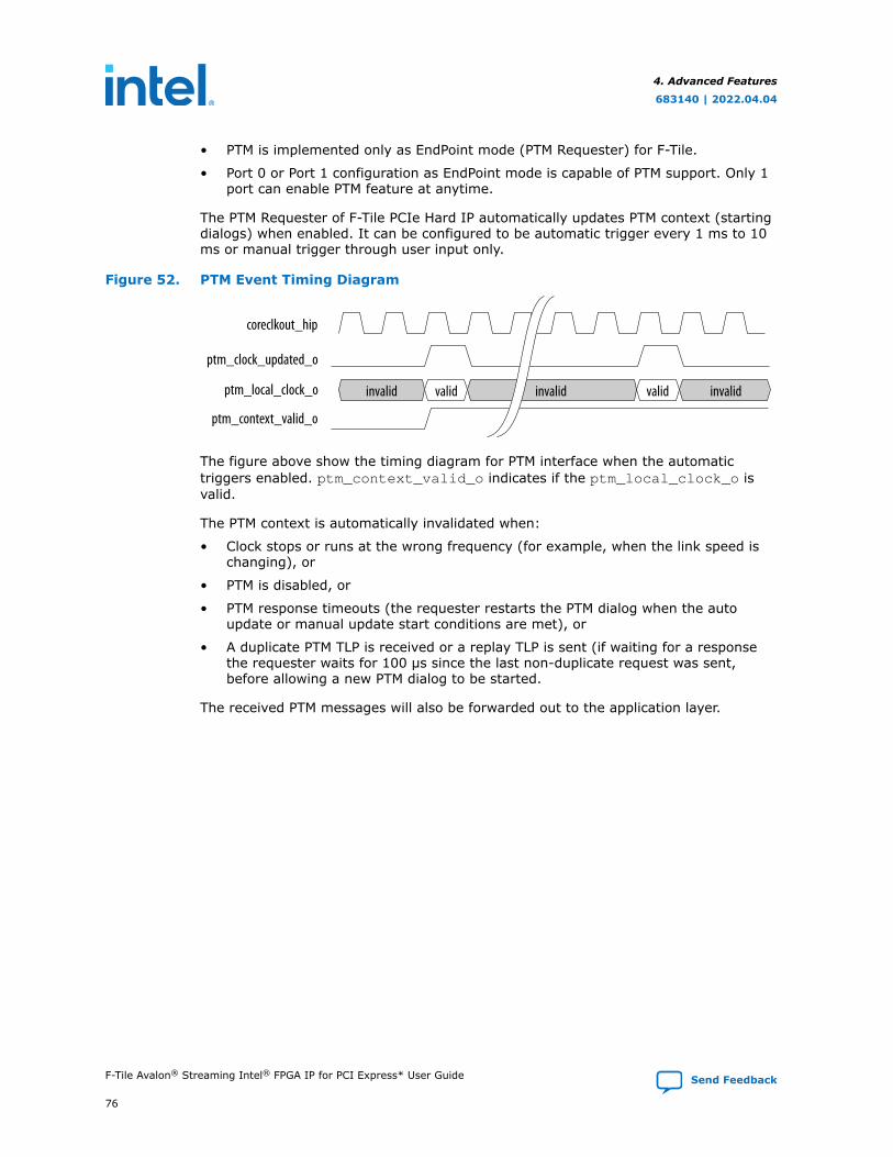
• PTM is implemented only as EndPoint mode (PTM Requester) for F-Tile.
• Port 0 or Port 1 configuration as EndPoint mode is capable of PTM support. Only 1port can enable PTM feature at anytime.
The PTM Requester of F-Tile PCIe Hard IP automatically updates PTM context (startingdialogs) when enabled. It can be configured to be automatic trigger every 1 ms to 10ms or manual trigger through user input only.
Figure 52. PTM Event Timing Diagram
coreclkout_hip
ptm_clock_updated_o
ptm_local_clock_o
ptm_context_valid_o
invalid invalid invalidvalid valid
The figure above show the timing diagram for PTM interface when the automatictriggers enabled. ptm_context_valid_o indicates if the ptm_local_clock_o isvalid.
The PTM context is automatically invalidated when:
• Clock stops or runs at the wrong frequency (for example, when the link speed ischanging), or
• PTM is disabled, or
• PTM response timeouts (the requester restarts the PTM dialog when the autoupdate or manual update start conditions are met), or
• A duplicate PTM TLP is received or a replay TLP is sent (if waiting for a responsethe requester waits for 100 μs since the last non-duplicate request was sent,before allowing a new PTM dialog to be started.
The received PTM messages will also be forwarded out to the application layer.
4. Advanced Features
683140 | 2022.04.04
F-Tile Avalon® Streaming Intel® FPGA IP for PCI Express* User Guide Send Feedback
76
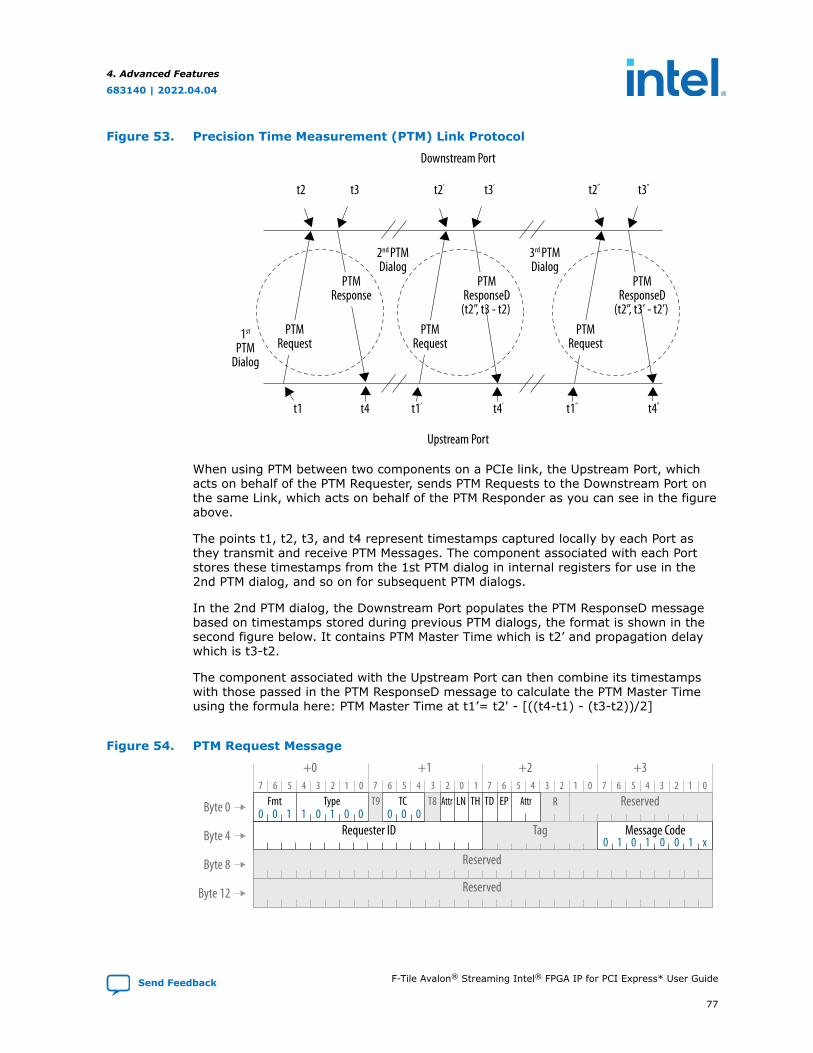
Figure 53. Precision Time Measurement (PTM) Link Protocol
PTMResponse
PTMRequest
PTMResponseD
(t2”, t3 - t2)PTM
Request
Upstream Port
Downstream Port
t1 t4 t1’ t4’ t1’’ t4’’
t2 t3 t2’ t3’ t2’’ t3’’
1st
PTMDialog
2nd PTMDialog
3rd PTMDialog
PTMResponseD
(t2”, t3’ - t2’)PTM
Request
When using PTM between two components on a PCIe link, the Upstream Port, whichacts on behalf of the PTM Requester, sends PTM Requests to the Downstream Port onthe same Link, which acts on behalf of the PTM Responder as you can see in the figureabove.
The points t1, t2, t3, and t4 represent timestamps captured locally by each Port asthey transmit and receive PTM Messages. The component associated with each Portstores these timestamps from the 1st PTM dialog in internal registers for use in the2nd PTM dialog, and so on for subsequent PTM dialogs.
In the 2nd PTM dialog, the Downstream Port populates the PTM ResponseD messagebased on timestamps stored during previous PTM dialogs, the format is shown in thesecond figure below. It contains PTM Master Time which is t2’ and propagation delaywhich is t3-t2.
The component associated with the Upstream Port can then combine its timestampswith those passed in the PTM ResponseD message to calculate the PTM Master Timeusing the formula here: PTM Master Time at t1’= t2' - [((t4-t1) - (t3-t2))/2]
Figure 54. PTM Request Message
+007 6 5 4 3 2 1 0
+17 6 5 4 3 2
+2 +31 7 6 5 4 3 2 1 0 7 6 5 4 3 2 1 0
Byte 0
Byte 4
Byte 8
Byte 12
Fmt Type T9 T8 LN THAttr AttrTC TD EP R Reserved
Reserved
Reserved
Message CodeRequester ID Tag0 0 0 0 0 0 001 1 1
0 1 0 1 00 1 x
4. Advanced Features
683140 | 2022.04.04
Send Feedback F-Tile Avalon® Streaming Intel® FPGA IP for PCI Express* User Guide
77
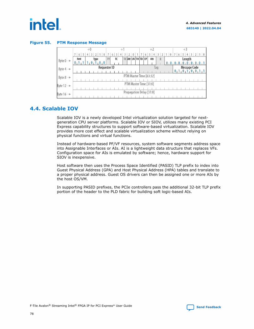
Figure 55. PTM Response Message
4.4. Scalable IOV
Scalable IOV is a newly developed Intel virtualization solution targeted for next-generation CPU server platforms. Scalable IOV or SIOV, utilizes many existing PCIExpress capability structures to support software-based virtualization. Scalable IOVprovides more cost effect and scalable virtualization scheme without relying onphysical functions and virtual functions.
Instead of hardware-based PF/VF resources, system software segments address spaceinto Assignable Interfaces or AIs. AI is a lightweight data structure that replaces VFs.Configuration space for AIs is emulated by software; hence, hardware support forSIOV is inexpensive.
Host software then uses the Process Space Identified (PASID) TLP prefix to index intoGuest Physical Address (GPA) and Host Physical Address (HPA) tables and translate toa proper physical address. Guest OS drivers can then be assigned one or more AIs bythe host OS/VM.
In supporting PASID prefixes, the PCIe controllers pass the additional 32-bit TLP prefixportion of the header to the PLD fabric for building soft logic-based AIs.
4. Advanced Features
683140 | 2022.04.04
F-Tile Avalon® Streaming Intel® FPGA IP for PCI Express* User Guide Send Feedback
78
5. InterfacesThis section focuses primarily on the signal interfaces that the F-Tile Avalon-ST IP forPCIe uses to communicate with the Application Layer in the FPGA fabric core.
5.1. Overview
By looking at the prefix of the signal names, you can determine the port origin of thesignal.
• p0: x16 core
• p1: x8 core
• p2: x4_0 core
• p3: x4_1 core
The figure below shows the top-level signals of this IP. Note that the signal names inthe figure will get the appropriate prefix pn (where n = 0, 1, 2 or 3) depending onwhich of the three supported configurations (1x16, 2x8, or 4x4) the F-Tile Avalon-STIP for PCI Express is present.
As an example, the rx_st_data_o bus can take on the following names:
• In the 1x16 configuration, only the x16 core is active. In this case, this busappears as p0_rx_st_data_o[511:0].
• In the 2x8 configuration, both the x16 core and x8 core are active. In this case,this bus is split into p0_rx_st_data_o[255:0] andp1_rx_st_data_o[255:0].
• In the 4x4 configuration, all four cores are active. In this case, this bus is splitinto p0_rx_st_data_o[127:0], p1_rx_st_data_o[127:0],p2_rx_st_data_o[127:0] and p3_rx_st_data_o[127:0].
The only cases where the interface signal names do not get the pn prefixes are theinterfaces that are common for all the cores, like the PHY reconfiguration interface,clocks and resets. For example, there is only one xcvr_reconfig_clk that is sharedby all the cores.
You can enable the PHY reconfiguration interface from the Top Level Settings in theGUI.
Each of the cores has its own Avalon-ST interface to the user logic. The number of IP-to-User Logic interfaces exposed to the FPGA fabric are different based on theconfiguration modes.
683140 | 2022.04.04
Send Feedback
Intel Corporation. All rights reserved. Intel, the Intel logo, and other Intel marks are trademarks of IntelCorporation or its subsidiaries. Intel warrants performance of its FPGA and semiconductor products to currentspecifications in accordance with Intel's standard warranty, but reserves the right to make changes to anyproducts and services at any time without notice. Intel assumes no responsibility or liability arising out of theapplication or use of any information, product, or service described herein except as expressly agreed to inwriting by Intel. Intel customers are advised to obtain the latest version of device specifications before relyingon any published information and before placing orders for products or services.*Other names and brands may be claimed as the property of others.
ISO9001:2015Registered
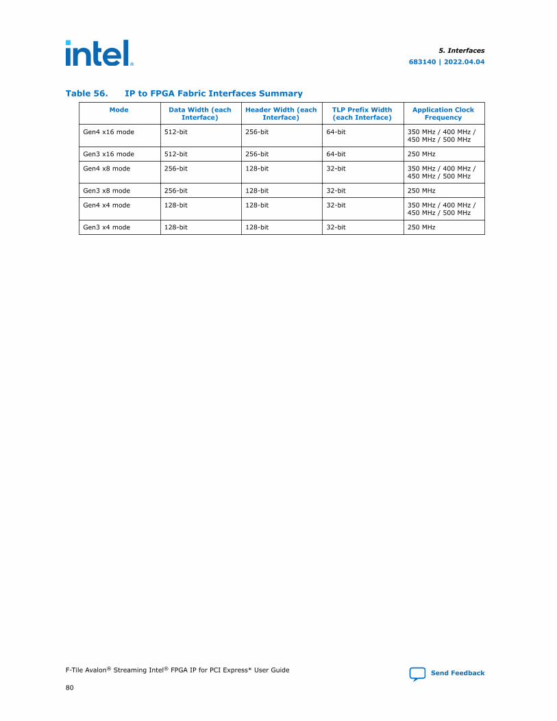
Table 56. IP to FPGA Fabric Interfaces Summary
Mode Data Width (eachInterface)
Header Width (eachInterface)
TLP Prefix Width(each Interface)
Application ClockFrequency
Gen4 x16 mode 512-bit 256-bit 64-bit 350 MHz / 400 MHz /450 MHz / 500 MHz
Gen3 x16 mode 512-bit 256-bit 64-bit 250 MHz
Gen4 x8 mode 256-bit 128-bit 32-bit 350 MHz / 400 MHz /450 MHz / 500 MHz
Gen3 x8 mode 256-bit 128-bit 32-bit 250 MHz
Gen4 x4 mode 128-bit 128-bit 32-bit 350 MHz / 400 MHz /450 MHz / 500 MHz
Gen3 x4 mode 128-bit 128-bit 32-bit 250 MHz
5. Interfaces
683140 | 2022.04.04
F-Tile Avalon® Streaming Intel® FPGA IP for PCI Express* User Guide Send Feedback
80
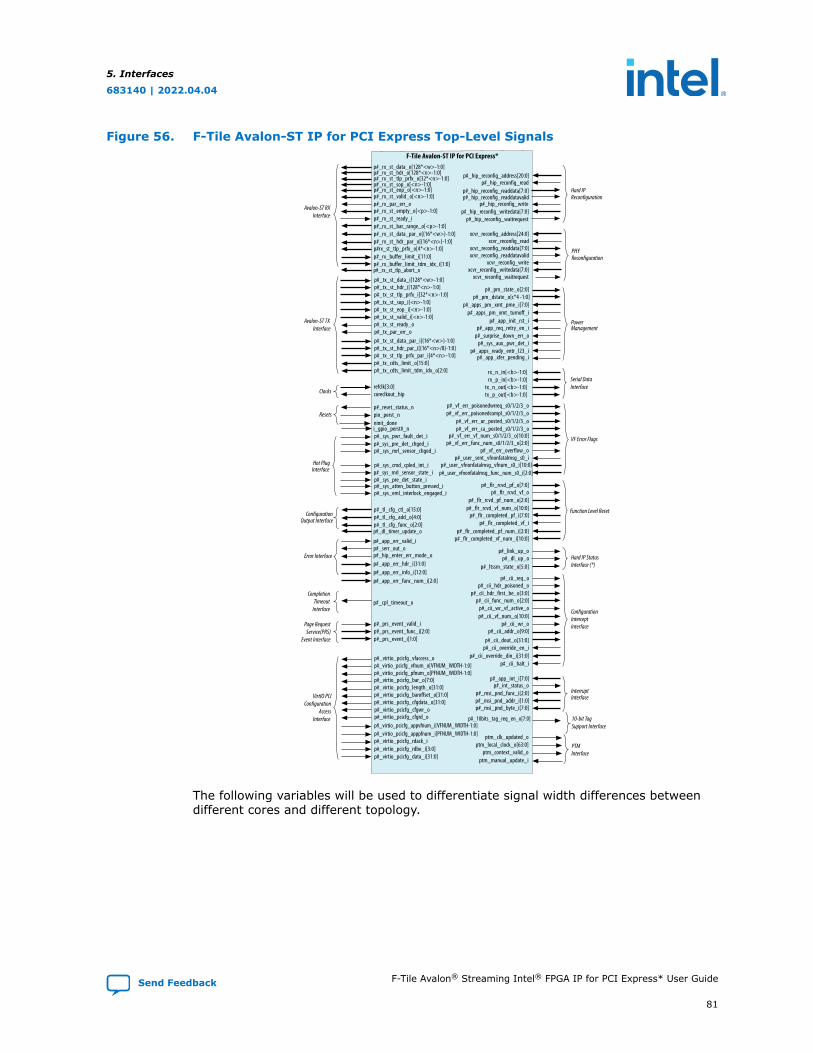
Figure 56. F-Tile Avalon-ST IP for PCI Express Top-Level Signals
p#_rx_st_data_o[128*<w>-1:0]
p#_rx_st_sop_o[<n>-1:0]p#_rx_st_eop_o[<n>-1:0]p#_rx_st_valid_o[<n>-1:0]
p#_rx_st_empty_o[<p>-1:0]p#_rx_st_ready_ip#_rx_st_bar_range_o[<p>-1:0]p#_rx_st_data_par_o[{16*<w>}-1:0]p#_rx_st_hdr_par_o[{16*<n>}-1:0]p#rx_st_tlp_prfx_o[4*<n>-1:0]
F-Tile Avalon-ST IP for PCI Express*
Avalon-ST RXInterface
Clocks
Resets
refclk[3:0]coreclkout_hip
pin_perst_np#_reset_status_n
p#_app_err_hdr_i[31:0]p#_app_err_info_i[12:0]p#_app_err_func_num_i[2:0]
p#_serr_out_op#_hip_enter_err_mode_oError Interface
p#_tl_cfg_add_o[4:0]p#_tl_cfg_ctl_o[15:0]
p#_tl_cfg_func_o[2:0]
ConfigurationOutput Interface
p#_prs_event_func_i[2:0]p#_prs_event_valid_i
p#_prs_event_i[1:0]
Page Request Service(PRS)
Event Interface
ptm_local_clock_o[63:0]ptm_clk_updated_o
ptm_context_valid_optm_manual_update_i
PTMInterface
p#_sys_aux_pwr_det_ip#_surprise_down_err_o
p#_apps_ready_entr_l23_ip#_app_xfer_pending_i
CompletionTimeout
Interface
p#_app_err_valid_i
p#_cpl_timeout_o
p#_rx_buffer_limit_i[11:0]p#_rx_buffer_limit_tdm_idx_i[1:0]
PowerManagement
Reconfiguration
p#_hip_reconfig_address[20:0]p#_hip_reconfig_read
p#_hip_reconfig_readdata[7:0]p#_hip_reconfig_readdatavalid
p#_hip_reconfig_writedata[7:0]p#_hip_reconfig_waitrequest
p#_hip_reconfig_write
p#_pm_state_o[2:0]p#_pm_dstate_o[c*4 -1:0]
p#_apps_pm_xmt_pme_i[7:0]p#_apps_pm_xmt_turnoff_i
p#_app_init_rst_ip#_app_req_retry_en_i
Function Level Reset
p#_flr_rcvd_pf_o[7:0]p#_flr_rcvd_vf_o
p#_flr_rcvd_pf_num_o[2:0]p#_flr_rcvd_vf_num_o[10:0]
p#_flr_completed_pf_i[7:0]p#_flr_completed_vf_i
p#_flr_completed_pf_num_i[2:0]p#_flr_completed_vf_num_i[10:0]
Hard IP StatusInterface (*)
p#_link_up_op#_dl_up_o
p#_int_status_o
p#_ltssm_state_o[5:0]
p#_rx_par_err_o
rx_n_in[<b>-1:0]rx_p_in[<b>-1:0]
tx_n_out[<b>-1:0]tx_p_out[<b>-1:0]
Serial Data Interface
p#_msi_pnd_func_i[2:0]p#_msi_pnd_addr_i[1:0]p#_msi_pnd_byte_i[7:0]
Interrupt Interface
ConfigurationInterceptInterface
p#_cii_req_op#_cii_hdr_poisoned_o
p#_cii_hdr_first_be_o[3:0]p#_cii_func_num_o[2:0]
p#_cii_wr_vf_active_op#_cii_vf_num_o[10:0]
p#_cii_wr_op#_cii_addr_o[9:0]
p#_cii_dout_o[31:0]p#_cii_override_en_i
p#_cii_override_din_i[31:0]p#_cii_halt_i
Hard IP
p#_rx_st_hdr_o[128*<n>-1:0]p#_rx_st_tlp_prfx_o[32*<n>-1:0]
Reconfiguration
xcvr_reconfig_address[24:0]xcvr_reconfig_read
xcvr_reconfig_readdata[7:0]xcvr_reconfig_readdatavalid
xcvr_reconfig_writedata[7:0]xcvr_reconfig_waitrequest
xcvr_reconfig_write
PHY
p#_app_int_i[7:0]
InterfaceHot Plug
p#_sys_pwr_fault_det_ip#_sys_pre_det_chged_ip#_sys_mrl_sensor_chged_i
p#_sys_cmd_cpled_int_ip#_sys_mrl_sensor_state_ip#_sys_pre_det_state_ip#_sys_atten_button_pressed_ip#_sys_eml_interlock_engaged_i
p#_tx_st_data_i[128*<w>-1:0]p#_tx_st_hdr_i[128*<n>-1:0]p#_tx_st_tlp_prfx_i[32*<n>-1:0]p#_tx_st_sop_i[<n>-1:0]p#_tx_st_eop_i[<n>-1:0]p#_tx_st_valid_i[<n>-1:0]p#_tx_st_ready_oAvalon-ST TX
Interface
p#_tx_st_hdr_par_i[{16*<n>/8}-1:0]p#_tx_st_tlp_prfx_par_i[4*<n>-1:0]p#_tx_cdts_limit_o[15:0]p#_tx_cdts_limit_tdm_idx_o[2:0]
p#_tx_st_data_par_i[{16*<w>}-1:0]p#_tx_par_err_o
p#_virtio_pcicfg_vfaccess_op#_virtio_pcicfg_vfnum_o[VFNUM_WIDTH-1:0]p#_virtio_pcicfg_pfnum_o[PFNUM_WIDTH-1:0]p#_virtio_pcicfg_bar_o[7:0]p#_virtio_pcicfg_length_o[31:0]p#_virtio_pcicfg_baroffset_o[31:0]p#_virtio_pcicfg_cfgdata_o[31:0]
VirtIO PCIConfiguration
AccessInterface
p#_virtio_pcicfg_apppfnum_i[PFNUM_WIDTH-1:0]p#_virtio_pcicfg_rdack_ip#_virtio_pcicfg_rdbe_i[3:0]p#_virtio_pcicfg_data_i[31:0]
p#_virtio_pcicfg_appvfnum_i[VFNUM_WIDTH-1:0]
p#_virtio_pcicfg_cfgwr_op#_virtio_pcicfg_cfgrd_o
ninit_done
p#_vf_err_poisonedwrreq_s0/1/2/3_o
VF Error Flags
p#_vf_err_poisonedcompl_s0/1/2/3_op#_vf_err_ur_posted_s0/1/2/3_op#_vf_err_ca_posted_s0/1/2/3_o
p#_vf_err_vf_num_s0/1/2/3_o[10:0]p#_vf_err_func_num_s0/1/2/3_o[2:0]
p#_vf_err_overflow_op#_user_sent_vfnonfatalmsg_s0_i
p#_user_vfnonfatalmsg_vfnum_s0_i[10:0]p#_user_vfnonfatalmsg_func_num_s0_i[2:0]
p#_dl_timer_update_o
p#_rx_st_tlp_abort_o
p#_10bits_tag_req_en_o[7:0] 10-bit Tag Support Interface
i_gpio_perst#_n
The following variables will be used to differentiate signal width differences betweendifferent cores and different topology.
5. Interfaces
683140 | 2022.04.04
Send Feedback F-Tile Avalon® Streaming Intel® FPGA IP for PCI Express* User Guide
81
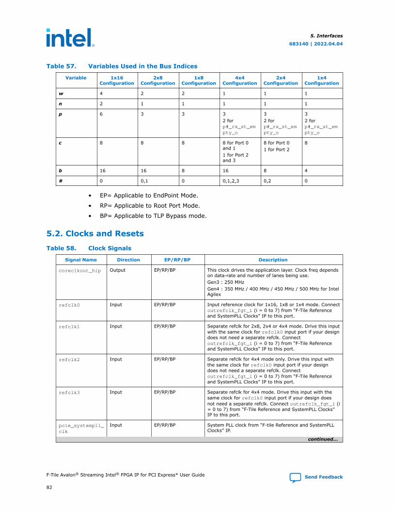
Table 57. Variables Used in the Bus Indices
Variable 1x16Configuration
2x8Configuration
1x8Configuration
4x4Configuration
2x4Configuration
1x4Configuration
w 4 2 2 1 1 1
n 2 1 1 1 1 1
p 6 3 3 32 forp#_rx_st_empty_o
32 forp#_rx_st_empty_o
32 forp#_rx_st_empty_o
c 8 8 8 8 for Port 0and 11 for Port 2and 3
8 for Port 01 for Port 2
8
b 16 16 8 16 8 4
# 0 0,1 0 0,1,2,3 0,2 0
• EP= Applicable to EndPoint Mode.
• RP= Applicable to Root Port Mode.
• BP= Applicable to TLP Bypass mode.
5.2. Clocks and Resets
Table 58. Clock Signals
Signal Name Direction EP/RP/BP Description
coreclkout_hip Output EP/RP/BP This clock drives the application layer. Clock freq dependson data-rate and number of lanes being use.Gen3 : 250 MHzGen4 : 350 MHz / 400 MHz / 450 MHz / 500 MHz for IntelAgilex
refclk0 Input EP/RP/BP Input reference clock for 1x16, 1x8 or 1x4 mode. Connectoutrefclk_fgt_i (i = 0 to 7) from “F-Tile Referenceand SystemPLL Clocks” IP to this port.
refclk1 Input EP/RP/BP Separate refclk for 2x8, 2x4 or 4x4 mode. Drive this inputwith the same clock for refclk0 input port if your designdoes not need a separate refclk. Connectoutrefclk_fgt_i (i = 0 to 7) from “F-Tile Referenceand SystemPLL Clocks” IP to this port.
refclk2 Input EP/RP/BP Separate refclk for 4x4 mode only. Drive this input withthe same clock for refclk0 input port if your designdoes not need a separate refclk. Connectoutrefclk_fgt_i (i = 0 to 7) from “F-Tile Referenceand SystemPLL Clocks” IP to this port.
refclk3 Input EP/RP/BP Separate refclk for 4x4 mode. Drive this input with thesame clock for refclk0 input port if your design doesnot need a separate refclk. Connect outrefclk_fgt_i (i= 0 to 7) from “F-Tile Reference and SystemPLL Clocks”IP to this port.
pcie_systempll_clk
Input EP/RP/BP System PLL clock from “F-tile Reference and SystemPLLClocks” IP.
continued...
5. Interfaces
683140 | 2022.04.04
F-Tile Avalon® Streaming Intel® FPGA IP for PCI Express* User Guide Send Feedback
82
Signal Name Direction EP/RP/BP Description
Connect out_systempll_clk_0 from the "F-TileReference and System PLL Clocks" IP to this port.For Mode of System PLL setting, select frequency that isTWO times of the selected PLD Clock Frequency. Forexample, if the selected PLD clock frequency is 500 MHz,use the "PCIE_FREQ_1000" setting.For Refclk source, select any of the enabled Refclk. Referto Refclk on page 16 for more information.
p#_hip_reconfig_clk
Input EP/RP/BP Clock for hip_reconfig interface. Frequency rangesfrom 50 MHz to 125 MHz.Note: Intel recommends using 100 MHz clock source for
HIP reconfig clock
xcvr_reconfig_clk
Input EP/RP/BP Clock for PHY reconfiguration interface. Frequency rangesfrom 50 MHz to 125 MHz.Note: Intel recommends using 100 MHz clock source for
PHY reconfig clock
Table 59. Reset Signals
Signal Name Direction EP/RP/BP Clock Domain Description
pin_perst_n Input EP/RP/BP Async This is an active-lowinput to PCIe Hard IPfor PERST# functiondefined by PCIespecification
p#_pin_perst_n Output EP/RP/BP Async PERST# statusindication for port#.When IndependentPerst is enabled,assertion of this signalis delayed for port#controlled bygpio_perst.
ninit_done Input EP/RP/BP Async From “Reset ReleaseIP”.A “1” on this active-low signal indicatesthat the FPGA deviceis not yet fullyconfigured.A “0” indicates thedevice has beenconfigured and is innormal operatingmode.
p#_reset_status_n Output EP/RP/BP coreclkout_hip Held low until PCIeport is out of reset.
i_gpio_perst#_n Input EP/BP async This is an active-lowreset to each portwhen IndependentPerst option isenabled.
5. Interfaces
683140 | 2022.04.04
Send Feedback F-Tile Avalon® Streaming Intel® FPGA IP for PCI Express* User Guide
83
5.3. Serial Data Interface
Table 60. Serial Data Interface Signals
Signal Name Direction EP/RP/BP Description
tx_p_out[b-1:0]
tx_n_out[b-1:0]
Output EP/RP/BP Trasnmit serial data outputusing High SpeedDifferential I/O Standard
rx_p_in[b-1:0]
rx_n_in[b-1:0]
Input EP/RP/BP Receive serial data outputusing High SpeedDifferential I/O Standard
5.4. Avalon-ST Interface
Note: Avalon-ST RX and TX interfaces have been described in detail in the previous chapteron Avalon-ST TX/RX on page 25. The following section provide information about theinterface signals only.
5.4.1. Avalon-ST RX Interface Signals
Table 61. Avalon-ST RX Interface Signals
Signal Name Direction EP/RP/BP Clock Domain Description
p#_rx_st_data_o[w*128-1:0]
Output EP/RP/BP coreclkout_hip Avalon-ST Rx databus. Applicationreceive RX data fromTransaction layer viathis bus.For Port0(width=512), TLP withan end-of-packet atthe lower 256 bits isallowed to have start-of-packet at the upper256 bits.
p#_rx_st_empty_o[p-1:0]
Output EP/RP/BP coreclkout_hip Specify the number ofdwords that are emptyduring cycles whenthe rx_st_eop_osignals are asserted.These signals are notvalid when therx_st_eop_o signalsare not asserted.
p#_rx_st_ready_i Input EP/RP/BP coreclkout_hip Indicates theApplication Layer isready to accept data.The readyLatency is27 cycles.If rx_st_ready_i isdeasserted by theApplication Layer oncycle <n>, theTransaction Layer inthe PCIe Hard IPcontinues to sendtraffic up to <n>
continued...
5. Interfaces
683140 | 2022.04.04
F-Tile Avalon® Streaming Intel® FPGA IP for PCI Express* User Guide Send Feedback
84
Signal Name Direction EP/RP/BP Clock Domain Description
+readyLatency cyclesafter the deassertionof rx_st_ready_i.Oncerx_st_ready_ireasserts,rx_st_valid_oresumes data transferwithin readyLatencycycles.To achieve the bestperformance, theApplication Layer mustinclude a receivebuffer large enough toavoid the deassertionof rx_st_ready_i.
p#_rx_st_sop_o[n-1:0]
Output EP/RP/BP coreclkout_hip Signals the first cycleof the TLP whenasserted inconjunction with thecorresponding bit ofrx_st_valid_o[1:0].rx_st_sop_o[1]:When asserted,signals the start of aTLP onrx_st_data_o[511:256].rx_st_sop_o[0]:When asserted,signals the start of aTLP onrx_st_data_o[255:0].
p#_rx_st_eop_o[n-1:0]
Output EP/RP/BP coreclkout_hip Signals the last cycleof the TLP whenasserted inconjunction with thecorresponding bit ofrx_st_valid_o[1:0].rx_st_eop_o[1]:When asserted,signals the end of aTLP onrx_st_data_o[511:256].rx_st_eop_o[0]:When asserted,signals the end of aTLP onrx_st_data_o[255:0].
p#_rx_st_valid_o[n-1:0]
Output EP/RP/BP coreclkout_hip These signals qualifythe rx_st_data_osignals going into theApplication Layer.
continued...
5. Interfaces
683140 | 2022.04.04
Send Feedback F-Tile Avalon® Streaming Intel® FPGA IP for PCI Express* User Guide
85

Signal Name Direction EP/RP/BP Clock Domain Description
p#_rx_st_hdr_o[n*128-1:0]
Output EP/RP/BP coreclkout_hip This is the receivedheader, which followsthe TLP header formatof the PCIespecifications.
p#_rx_st_tlp_prfx_o[n*32-1:0]
Output EP/RP/BP coreclkout_hip This is the first TLPprefix received, whichfollows the TLP prefixformat of the PCIespecifications. PASIDis included.These signals are validwhen thecorrespondingrx_st_sop_o isasserted.The TLP prefix uses aBig Endianimplementation (i.e,the Fmt field is in bits[31:29] and the Typefield is in bits[28:24]).If no prefix is presentfor a given TLP, thatdword (including theFmt field) is all zeros.
p#_rx_st_vf_active_o[n-1:0]
Output EP coreclkout_hip Note: Not available forp2 and p3.When asserted, thesesignals indicate thatthe received TLP istargeting a virtualfunction.When these signalsare deasserted, thereceived TLP istargeting a physicalfunction and therx_st_func_numsignals indicate thefunction number.These signals are validwhen thecorrespondingrx_st_sop_o isasserted. Thesesignals aremultiplexed with therx_st_hdr_o signals inthe x4 configuration.These signals are validin Endpoint modeonly.
p#_rx_st_func_num_o[p-1:0]
Output EP coreclkout_hip Note: Not available forp2 and p3.Specify the targetphysical functionnumber for thereceived TLP.
continued...
5. Interfaces
683140 | 2022.04.04
F-Tile Avalon® Streaming Intel® FPGA IP for PCI Express* User Guide Send Feedback
86
Signal Name Direction EP/RP/BP Clock Domain Description
These signals are validwhen thecorrespondingrx_st_sop_o isasserted.These signals aremultiplexed with therx_st_hdr_o signals inthe x4 configuration.These signals are validin Endpoint modeonly.
p#_rx_st_vf_num_o[n*11-1:0]
Output EP coreclkout_hip Note: Not available forp2 and p3.Specify the target VFmnumber for thereceived TLP.The application usesthis information forboth request andcompletion TLPs.For a completion TLP,these bits specify theVF number of therequester for thiscompletion TLP.These signals are validwhenrx_st_vf_active_o andthe correspondingrx_st_sop_o areasserted.These signals aremultiplexed with therx_st_hdr_o signals inthe x4 configuration.These signals are validin Endpoint modeonly.
p#_rx_st_bar_range_o[p-1:0]
Output EP/RP/BP coreclkout_hip Specify the BAR forthe TLP being output.For each BAR range,the followingencodings aredefined:• 000: Memory BAR
0• 001: Memory BAR
1• 010: Memory BAR
2• 011: Memory BAR
3• 100: Memory BAR
4• 101: Memory BAR
5• 110: I/O BAR• 111: Expansion
ROM BAR
continued...
5. Interfaces
683140 | 2022.04.04
Send Feedback F-Tile Avalon® Streaming Intel® FPGA IP for PCI Express* User Guide
87
Signal Name Direction EP/RP/BP Clock Domain Description
These outputs arevalid when bothrx_st_sop_o andrx_st_valid_o areasserted.
p#_rx_st_tlp_abort_o[n-1:0]
Output BP coreclkout_hip Indicates toapplication to drop theTLP because of ECRCerror. You should notexpect the TLP to bereplayed.By default, PCIe hipdrop errored TLP.Operating in TLPBypass mode, erroredTLPs will be forwardedto the RX packetinterface.This output is validwhen rx_st_valid_o isasserted.
p#_rx_st_data_par_o[w*16-1:0]
Output EP/RP/BP coreclkout_hip Byte parity signals forrx_st_data_o.These parity signalsare not available whenECC is enabled.
p#_rx_st_hdr_par_o[n*16-1:0]
Output EP/RP/BP coreclkout_hip Byte parity signals forrx_st_hdr_o. Theseparity signals are notavailable when ECC isenabled.
p#_rx_st_tlp_prfx_par_o[n*4-1:0]
Output EP/RP/BP coreclkout_hip Byte parity signals forrx_st_tlp_prfx_o.These parity signalsare not available whenECC is enabled.
p#_rx_par_err_o Output EP/RP/BP coreclkout_hip Asserted for a singlecycle to indicate that aparity error wasdetected in a TLP atthe input of the RXbuffer.This error is logged asan uncorrectableinternal error in theVSEC registers.If this error occurs,you must reset theHard IP because parityerrors can leave theHard IP in anunknown state.
5. Interfaces
683140 | 2022.04.04
F-Tile Avalon® Streaming Intel® FPGA IP for PCI Express* User Guide Send Feedback
88
Table 62. RX Flow Control Interface Signals
Signal Name Direction EP/RP/BP Clock Domain Description
p#_rx_buffer_limit_tdm_indx_i[1:0]
Input EP/RP/BP coreclkout_hip These signals indicatethe type of buffer forthe correspondingrx_buffer_limit_i[11:0] signals.The Application Layershould provide thebuffer limitinformation for all theenabled ports in aTDM manner.The followingencodings aredefined:• 00: buffer limit for
P type of TLPs.• 01: buffer limit for
NP type.• 10: buffer limit for
CPL type.• 11: reserved.
p#_rx_buffer_limit_i[11:0]
Input EP/RP/BP coreclkout_hip When the RX FlowControl Interface isenabled, theapplication can usethese signals for TLPflow control.These signals indicatethe application RXbuffer space madeavailable since reset/initialization.Initially, the signalsare set according tothe buffer size (interms of the numberof TLPs the RX buffercan take).The value of thesesignals alwaysincrements and rollsover. For example, ifthe initial value is0xfff, therx_buffer_limit_i[11:0] valueincrements by 1 androlls over to 0x000when one receivedTLP exits theapplication RX buffer.If a TLP type isblocked due to a lackof the correspondingRX buffer space in theapplication layer, otherTLP types may bypassit per the PCIetransaction orderingrules.
continued...
5. Interfaces
683140 | 2022.04.04
Send Feedback F-Tile Avalon® Streaming Intel® FPGA IP for PCI Express* User Guide
89
Signal Name Direction EP/RP/BP Clock Domain Description
Note that the initialvalue ofrx_buffer_limit_i[11:0] cannot belarger than 2048 TLPs.
5.4.2. Avalon-ST TX Interface Signals
Table 63. Avalon-ST TX Interface Signals
Signal Name Direction EP/RP/BP Clock Domain Description
p#_tx_st_data_i[w*128-1:0]
Input EP/RP/BP coreclkout_hip Application Layer datafor transmission. TheApplication Layer mustprovide a properlyformatted TLP on theTX interface. Validwhen thecorrespondingtx_st_valid_i signal isasserted.The mapping ofmessage TLPs is thesame as the mappingof Transaction LayerTLPs with 4-dwordheaders. The numberof data cycles must becorrect for the lengthand address fields inthe header. Issuing apacket with anincorrect number ofdata cycles results inthe TX interfacehanging and becomingunable to acceptfurther requests.Note: There must beno Idle cycle betweenthe tx_st_sop_i andtx_st_eop_i cyclesunless there isbackpressure with thedeassertion oftx_st_ready_o.
p#_tx_st_sop_i[n-1:0]
Input EP/RP/BP coreclkout_hip Indicate the first cycleof a TLP whenasserted inconjunction with thecorresponding bit oftx_st_valid_i.For the x16configuration:
continued...
5. Interfaces
683140 | 2022.04.04
F-Tile Avalon® Streaming Intel® FPGA IP for PCI Express* User Guide Send Feedback
90
Signal Name Direction EP/RP/BP Clock Domain Description
• tx_st_sop_i[1]:When asserted,indicates the startof aTLP intx_st_data_i[511:256].
• tx_st_sop_i[0]:When asserted,indicates the startof a TLP intx_st_data_i[255:0].
These signals areasserted for one clockcycle per each TLP.They also qualify thecorrespondingtx_st_hdr_i andtx_st_tlp_prfx_isignals.
p#_tx_st_eop_i[n-1:0]
Input EP/RP/BP coreclkout_hip Indicate the last cycleof a TLP whenasserted inconjunction with thecorresponding bit oftx_st_valid_i.For the x16configuration:• tx_st_eop_i[1]:
When asserted,indicates the endof a TLP intx_st_data_i[511:256].
• tx_st_eop_i[0]:When asserted,indicates the endof a TLP intx_st_data_i[255:0].
These signals areasserted for one clockcycle per each TLP.
p#_tx_st_valid_i[n-1:0]
Input EP/RP/BP coreclkout_hip Qualify thecorresponding datasegment oftx_st_data_i into theIP core on readycycles.To facilitate timingclosure, it’srecommended thatuser register both thetx_st_ready_o andtx_st_valid_i signals.Note: There must beno Idle cycle betweenthe tx_st_sop_i andtx_st_eop_i cyclesunless there isbackpressure with thedeassertion oftx_st_ready_o.
continued...
5. Interfaces
683140 | 2022.04.04
Send Feedback F-Tile Avalon® Streaming Intel® FPGA IP for PCI Express* User Guide
91

Signal Name Direction EP/RP/BP Clock Domain Description
p#_tx_st_ready_o Output EP/RP/BP coreclkout_hip Indicates that thePCIe Hard IP is readyto accept data fortransmission. ThereadyLatency is threecycles.If tx_st_ready_o isasserted by theTransaction Layer inthe PCIe Hard IP oncycle <n>, then <n>+readyLatency is aready cycle, duringwhich the Applicationmay asserttx_st_valid_i andtransfer data.If tx_st_ready_o isdeasserted by theTransaction Layer oncycle <n>, then theApplication mustdeassert tx_st_valid_iwithin thereadyLatency numberof cycles after cycle<n>.tx_st_ready_o can bedeasserted in thefollowing conditions:• The LTSSM is not
ready.• A Retry is in
progress.• There are not
enough creditsavailable to sendthe request.
• The F-Tile Avalon-ST IP is busysending internallygenerated TLPs.
• The internal F-TileTX FIFO is full.
p#_tx_st_err_i[n-1:0]
Input EP/RP/BP coreclkout_hip When asserted,indicate an error inthe transmitted TLP.These signals areasserted withtx_st_eop_i and nullifya packet.tx_st_err_i[1]: Whenasserted, specifies anerror intx_st_data_i[511:256].tx_st_err_i[0]: Whenasserted, specifies anerror intx_st_data_i[255:0].
p#_tx_st_hdr_i[n*128-1:0]
Input EP/RP/BP coreclkout_hip This is the header tobe transmitted, whichfollows the TLP header
continued...
5. Interfaces
683140 | 2022.04.04
F-Tile Avalon® Streaming Intel® FPGA IP for PCI Express* User Guide Send Feedback
92
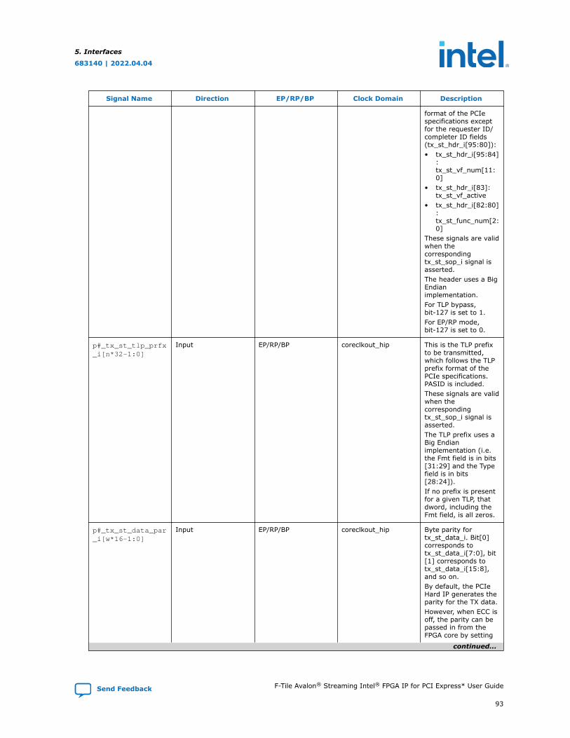
Signal Name Direction EP/RP/BP Clock Domain Description
format of the PCIespecifications exceptfor the requester ID/completer ID fields(tx_st_hdr_i[95:80]):• tx_st_hdr_i[95:84]
:tx_st_vf_num[11:0]
• tx_st_hdr_i[83]:tx_st_vf_active
• tx_st_hdr_i[82:80]:tx_st_func_num[2:0]
These signals are validwhen thecorrespondingtx_st_sop_i signal isasserted.The header uses a BigEndianimplementation.For TLP bypass,bit-127 is set to 1.For EP/RP mode,bit-127 is set to 0.
p#_tx_st_tlp_prfx_i[n*32-1:0]
Input EP/RP/BP coreclkout_hip This is the TLP prefixto be transmitted,which follows the TLPprefix format of thePCIe specifications.PASID is included.These signals are validwhen thecorrespondingtx_st_sop_i signal isasserted.The TLP prefix uses aBig Endianimplementation (i.e.the Fmt field is in bits[31:29] and the Typefield is in bits[28:24]).If no prefix is presentfor a given TLP, thatdword, including theFmt field, is all zeros.
p#_tx_st_data_par_i[w*16-1:0]
Input EP/RP/BP coreclkout_hip Byte parity fortx_st_data_i. Bit[0]corresponds totx_st_data_i[7:0], bit[1] corresponds totx_st_data_i[15:8],and so on.By default, the PCIeHard IP generates theparity for the TX data.However, when ECC isoff, the parity can bepassed in from theFPGA core by setting
continued...
5. Interfaces
683140 | 2022.04.04
Send Feedback F-Tile Avalon® Streaming Intel® FPGA IP for PCI Express* User Guide
93
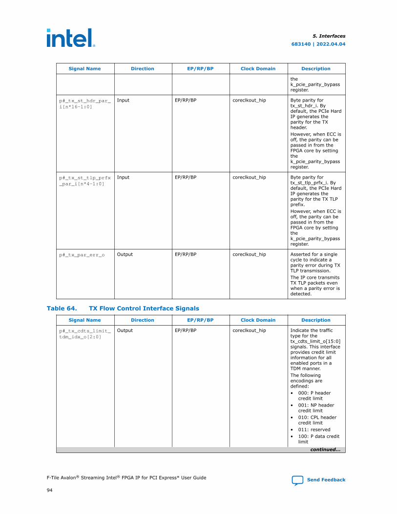
Signal Name Direction EP/RP/BP Clock Domain Description
thek_pcie_parity_bypassregister.
p#_tx_st_hdr_par_i[n*16-1:0]
Input EP/RP/BP coreclkout_hip Byte parity fortx_st_hdr_i. Bydefault, the PCIe HardIP generates theparity for the TXheader.However, when ECC isoff, the parity can bepassed in from theFPGA core by settingthek_pcie_parity_bypassregister.
p#_tx_st_tlp_prfx_par_i[n*4-1:0]
Input EP/RP/BP coreclkout_hip Byte parity fortx_st_tlp_prfx_i. Bydefault, the PCIe HardIP generates theparity for the TX TLPprefix.However, when ECC isoff, the parity can bepassed in from theFPGA core by settingthek_pcie_parity_bypassregister.
p#_tx_par_err_o Output EP/RP/BP coreclkout_hip Asserted for a singlecycle to indicate aparity error during TXTLP transmission.The IP core transmitsTX TLP packets evenwhen a parity error isdetected.
Table 64. TX Flow Control Interface Signals
Signal Name Direction EP/RP/BP Clock Domain Description
p#_tx_cdts_limit_tdm_idx_o[2:0]
Output EP/RP/BP coreclkout_hip Indicate the traffictype for thetx_cdts_limit_o[15:0]signals. This interfaceprovides credit limitinformation for allenabled ports in aTDM manner.The followingencodings aredefined:• 000: P header
credit limit• 001: NP header
credit limit• 010: CPL header
credit limit• 011: reserved• 100: P data credit
limit
continued...
5. Interfaces
683140 | 2022.04.04
F-Tile Avalon® Streaming Intel® FPGA IP for PCI Express* User Guide Send Feedback
94
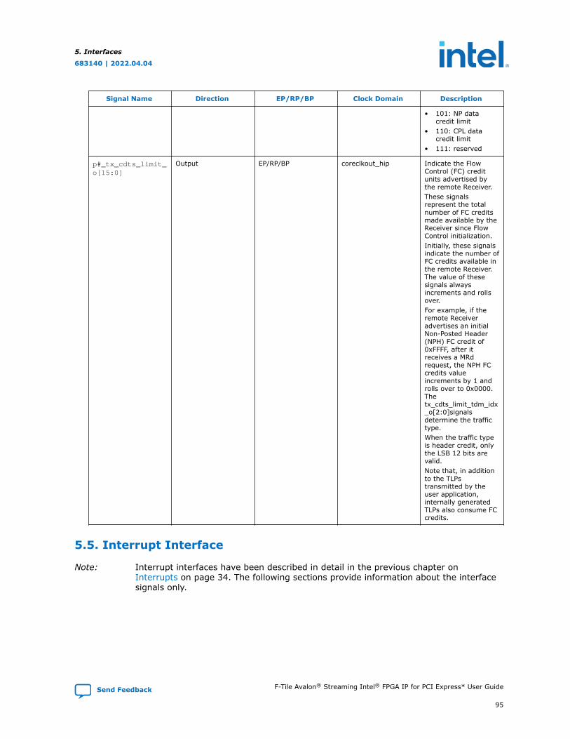
Signal Name Direction EP/RP/BP Clock Domain Description
• 101: NP datacredit limit
• 110: CPL datacredit limit
• 111: reserved
p#_tx_cdts_limit_o[15:0]
Output EP/RP/BP coreclkout_hip Indicate the FlowControl (FC) creditunits advertised bythe remote Receiver.These signalsrepresent the totalnumber of FC creditsmade available by theReceiver since FlowControl initialization.Initially, these signalsindicate the number ofFC credits available inthe remote Receiver.The value of thesesignals alwaysincrements and rollsover.For example, if theremote Receiveradvertises an initialNon-Posted Header(NPH) FC credit of0xFFFF, after itreceives a MRdrequest, the NPH FCcredits valueincrements by 1 androlls over to 0x0000.Thetx_cdts_limit_tdm_idx_o[2:0]signalsdetermine the traffictype.When the traffic typeis header credit, onlythe LSB 12 bits arevalid.Note that, in additionto the TLPstransmitted by theuser application,internally generatedTLPs also consume FCcredits.
5.5. Interrupt Interface
Note: Interrupt interfaces have been described in detail in the previous chapter on Interrupts on page 34. The following sections provide information about the interfacesignals only.
5. Interfaces
683140 | 2022.04.04
Send Feedback F-Tile Avalon® Streaming Intel® FPGA IP for PCI Express* User Guide
95
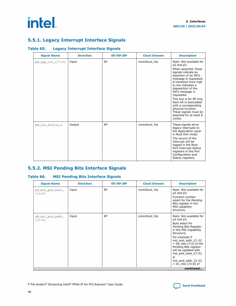
5.5.1. Legacy Interrupt Interface Signals
Table 65. Legacy Interrupt Interface Signals
Signal Name Direction EP/RP/BP Clock Domain Description
p#_app_int_i[7:0] Input EP coreclkout_hip Note: Not available forp2 and p3.When asserted, thesesignals indicate anassertion of an INTxmessage is requested.A transition from highto low indicates adeassertion of theINTx message isrequested.This bus is for EP only.Each bit is associatedwith a correspondingphysical function.These signals must beasserted for at least 8cycles.
p#_int_status_o Output RP coreclkout_hip These signals drivelegacy interrupts tothe Application Layerin Root Port mode.The source of theinterrupt will belogged in the RootPort Interrupt Statusregisters in the PortConfiguration andStatus registers.
5.5.2. MSI Pending Bits Interface Signals
Table 66. MSI Pending Bits Interface Signals
Signal Name Direction EP/RP/BP Clock Domain Description
p#_msi_pnd_func_i[2:0]
Input EP coreclkout_hip Note: Not available forp2 and p3.Function numberselect for the PendingBits register in theMSI capabilitystructure.
p#_msi_pnd_addr_i[1:0]
Input EP coreclkout_hip Note: Not available forp2 and p3.Byte select forPending Bits Registerin the MSI CapabilityStructure.For example ifmsi_pnd_addr_i[1:0]= 00, bits [7:0] of thePending Bits registerwill be updated withmsi_pnd_byte_i[7:0].Ifmsi_pnd_addr_i[1:0]= 01, bits [15:8] of
continued...
5. Interfaces
683140 | 2022.04.04
F-Tile Avalon® Streaming Intel® FPGA IP for PCI Express* User Guide Send Feedback
96
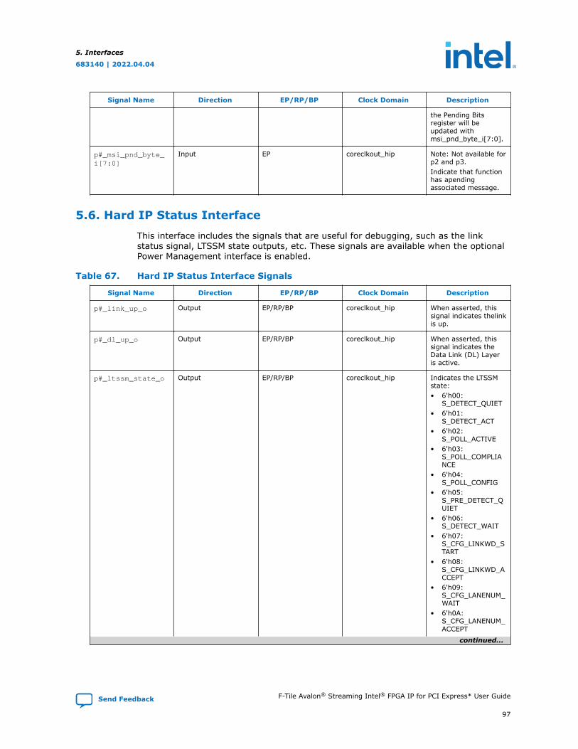
Signal Name Direction EP/RP/BP Clock Domain Description
the Pending Bitsregister will beupdated withmsi_pnd_byte_i[7:0].
p#_msi_pnd_byte_i[7:0]
Input EP coreclkout_hip Note: Not available forp2 and p3.Indicate that functionhas apendingassociated message.
5.6. Hard IP Status Interface
This interface includes the signals that are useful for debugging, such as the linkstatus signal, LTSSM state outputs, etc. These signals are available when the optionalPower Management interface is enabled.
Table 67. Hard IP Status Interface Signals
Signal Name Direction EP/RP/BP Clock Domain Description
p#_link_up_o Output EP/RP/BP coreclkout_hip When asserted, thissignal indicates thelinkis up.
p#_dl_up_o Output EP/RP/BP coreclkout_hip When asserted, thissignal indicates theData Link (DL) Layeris active.
p#_ltssm_state_o Output EP/RP/BP coreclkout_hip Indicates the LTSSMstate:• 6'h00:
S_DETECT_QUIET• 6'h01:
S_DETECT_ACT• 6'h02:
S_POLL_ACTIVE• 6'h03:
S_POLL_COMPLIANCE
• 6'h04:S_POLL_CONFIG
• 6'h05:S_PRE_DETECT_QUIET
• 6'h06:S_DETECT_WAIT
• 6'h07:S_CFG_LINKWD_START
• 6'h08:S_CFG_LINKWD_ACCEPT
• 6'h09:S_CFG_LANENUM_WAIT
• 6'h0A:S_CFG_LANENUM_ACCEPT
continued...
5. Interfaces
683140 | 2022.04.04
Send Feedback F-Tile Avalon® Streaming Intel® FPGA IP for PCI Express* User Guide
97
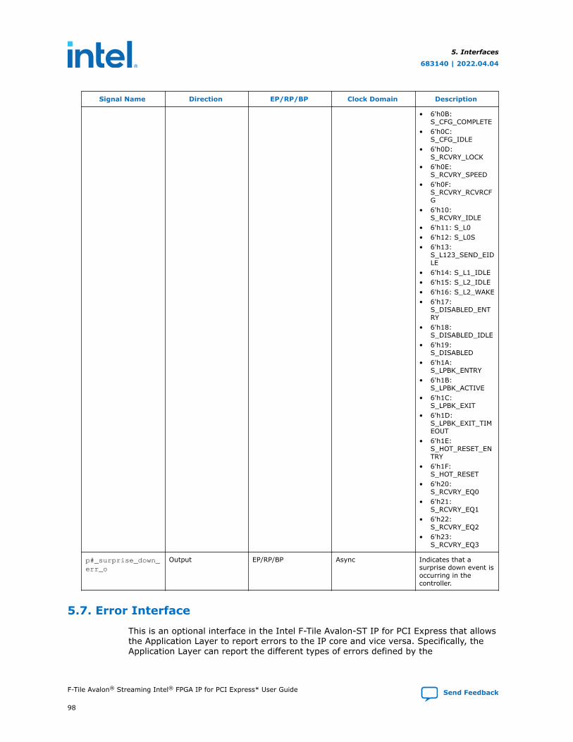
Signal Name Direction EP/RP/BP Clock Domain Description
• 6'h0B:S_CFG_COMPLETE
• 6'h0C:S_CFG_IDLE
• 6'h0D:S_RCVRY_LOCK
• 6'h0E:S_RCVRY_SPEED
• 6'h0F:S_RCVRY_RCVRCFG
• 6'h10:S_RCVRY_IDLE
• 6'h11: S_L0• 6'h12: S_L0S• 6'h13:
S_L123_SEND_EIDLE
• 6'h14: S_L1_IDLE• 6'h15: S_L2_IDLE• 6'h16: S_L2_WAKE• 6'h17:
S_DISABLED_ENTRY
• 6'h18:S_DISABLED_IDLE
• 6'h19:S_DISABLED
• 6'h1A:S_LPBK_ENTRY
• 6'h1B:S_LPBK_ACTIVE
• 6'h1C:S_LPBK_EXIT
• 6'h1D:S_LPBK_EXIT_TIMEOUT
• 6'h1E:S_HOT_RESET_ENTRY
• 6'h1F:S_HOT_RESET
• 6'h20:S_RCVRY_EQ0
• 6'h21:S_RCVRY_EQ1
• 6'h22:S_RCVRY_EQ2
• 6'h23:S_RCVRY_EQ3
p#_surprise_down_err_o
Output EP/RP/BP Async Indicates that asurprise down event isoccurring in thecontroller.
5.7. Error Interface
This is an optional interface in the Intel F-Tile Avalon-ST IP for PCI Express that allowsthe Application Layer to report errors to the IP core and vice versa. Specifically, theApplication Layer can report the different types of errors defined by the
5. Interfaces
683140 | 2022.04.04
F-Tile Avalon® Streaming Intel® FPGA IP for PCI Express* User Guide Send Feedback
98
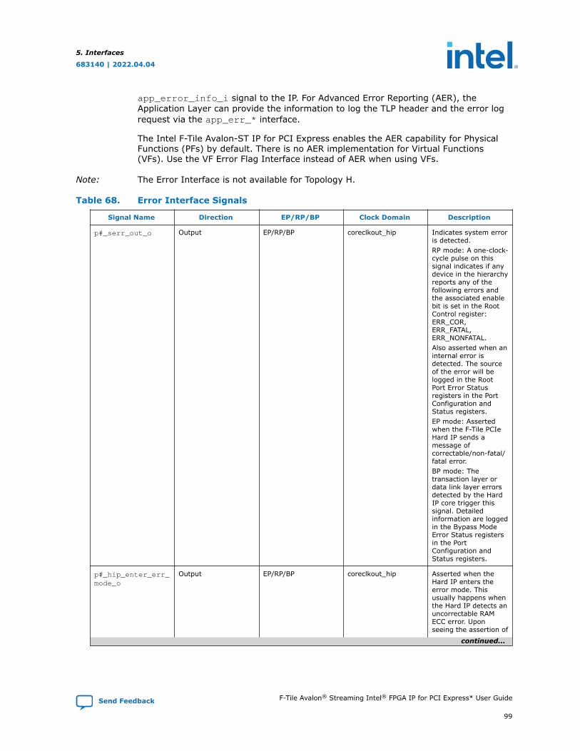
app_error_info_i signal to the IP. For Advanced Error Reporting (AER), theApplication Layer can provide the information to log the TLP header and the error logrequest via the app_err_* interface.
The Intel F-Tile Avalon-ST IP for PCI Express enables the AER capability for PhysicalFunctions (PFs) by default. There is no AER implementation for Virtual Functions(VFs). Use the VF Error Flag Interface instead of AER when using VFs.
Note: The Error Interface is not available for Topology H.
Table 68. Error Interface Signals
Signal Name Direction EP/RP/BP Clock Domain Description
p#_serr_out_o Output EP/RP/BP coreclkout_hip Indicates system erroris detected.RP mode: A one-clock-cycle pulse on thissignal indicates if anydevice in the hierarchyreports any of thefollowing errors andthe associated enablebit is set in the RootControl register:ERR_COR,ERR_FATAL,ERR_NONFATAL.Also asserted when aninternal error isdetected. The sourceof the error will belogged in the RootPort Error Statusregisters in the PortConfiguration andStatus registers.EP mode: Assertedwhen the F-Tile PCIeHard IP sends amessage ofcorrectable/non-fatal/fatal error.BP mode: Thetransaction layer ordata link layer errorsdetected by the HardIP core trigger thissignal. Detailedinformation are loggedin the Bypass ModeError Status registersin the PortConfiguration andStatus registers.
p#_hip_enter_err_mode_o
Output EP/RP/BP coreclkout_hip Asserted when theHard IP enters theerror mode. Thisusually happens whenthe Hard IP detects anuncorrectable RAMECC error. Uponseeing the assertion of
continued...
5. Interfaces
683140 | 2022.04.04
Send Feedback F-Tile Avalon® Streaming Intel® FPGA IP for PCI Express* User Guide
99
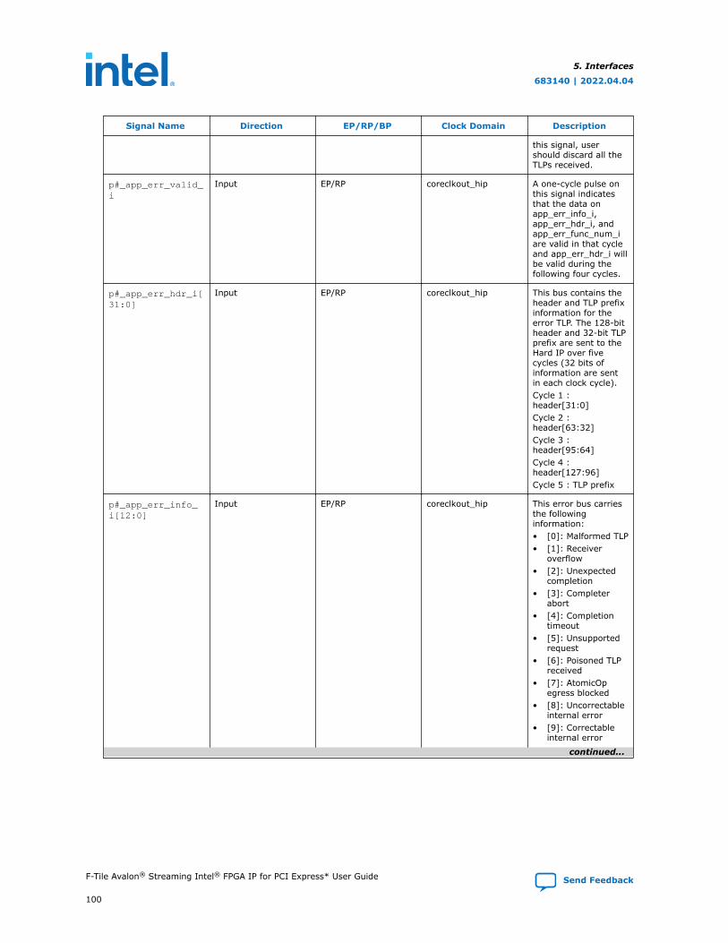
Signal Name Direction EP/RP/BP Clock Domain Description
this signal, usershould discard all theTLPs received.
p#_app_err_valid_i
Input EP/RP coreclkout_hip A one-cycle pulse onthis signal indicatesthat the data onapp_err_info_i,app_err_hdr_i, andapp_err_func_num_iare valid in that cycleand app_err_hdr_i willbe valid during thefollowing four cycles.
p#_app_err_hdr_i[31:0]
Input EP/RP coreclkout_hip This bus contains theheader and TLP prefixinformation for theerror TLP. The 128-bitheader and 32-bit TLPprefix are sent to theHard IP over fivecycles (32 bits ofinformation are sentin each clock cycle).Cycle 1 :header[31:0]Cycle 2 :header[63:32]Cycle 3 :header[95:64]Cycle 4 :header[127:96]Cycle 5 : TLP prefix
p#_app_err_info_i[12:0]
Input EP/RP coreclkout_hip This error bus carriesthe followinginformation:• [0]: Malformed TLP• [1]: Receiver
overflow• [2]: Unexpected
completion• [3]: Completer
abort• [4]: Completion
timeout• [5]: Unsupported
request• [6]: Poisoned TLP
received• [7]: AtomicOp
egress blocked• [8]: Uncorrectable
internal error• [9]: Correctable
internal error
continued...
5. Interfaces
683140 | 2022.04.04
F-Tile Avalon® Streaming Intel® FPGA IP for PCI Express* User Guide Send Feedback
100
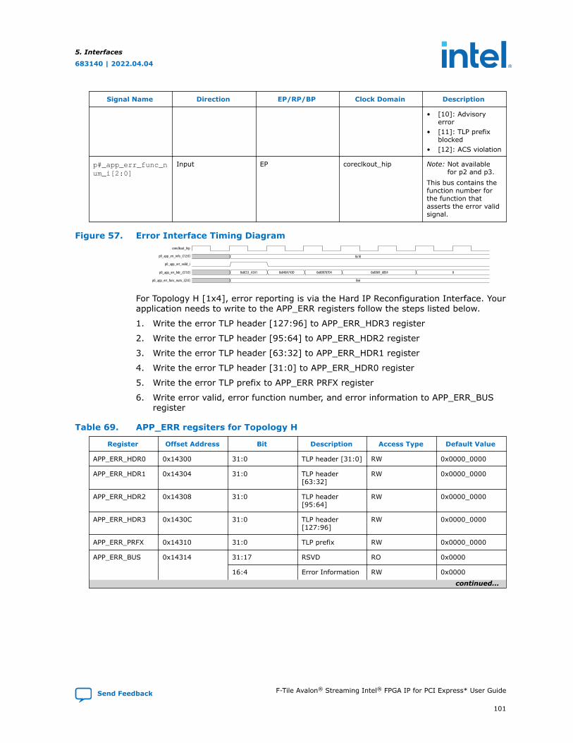
Signal Name Direction EP/RP/BP Clock Domain Description
• [10]: Advisoryerror
• [11]: TLP prefixblocked
• [12]: ACS violation
p#_app_err_func_num_i[2:0]
Input EP coreclkout_hip Note: Not availablefor p2 and p3.
This bus contains thefunction number forthe function thatasserts the error validsignal.
Figure 57. Error Interface Timing Diagramcoreclkout_hip
p0_app_err_info_i[12:0]
p0_app_err_valid_i
p0_app_err_hdr_i[31:0] 0x8C53_A3A1 0x840A743D 0x80B787D4 0x8DA9_6BE4 0
0x6
0x10
p0_app_err_func_num_i[2:0]
For Topology H [1x4], error reporting is via the Hard IP Reconfiguration Interface. Yourapplication needs to write to the APP_ERR registers follow the steps listed below.
1. Write the error TLP header [127:96] to APP_ERR_HDR3 register
2. Write the error TLP header [95:64] to APP_ERR_HDR2 register
3. Write the error TLP header [63:32] to APP_ERR_HDR1 register
4. Write the error TLP header [31:0] to APP_ERR_HDR0 register
5. Write the error TLP prefix to APP_ERR PRFX register
6. Write error valid, error function number, and error information to APP_ERR_BUSregister
Table 69. APP_ERR regsiters for Topology H
Register Offset Address Bit Description Access Type Default Value
APP_ERR_HDR0 0x14300 31:0 TLP header [31:0] RW 0x0000_0000
APP_ERR_HDR1 0x14304 31:0 TLP header[63:32]
RW 0x0000_0000
APP_ERR_HDR2 0x14308 31:0 TLP header[95:64]
RW 0x0000_0000
APP_ERR_HDR3 0x1430C 31:0 TLP header[127:96]
RW 0x0000_0000
APP_ERR_PRFX 0x14310 31:0 TLP prefix RW 0x0000_0000
APP_ERR_BUS 0x14314 31:17 RSVD RO 0x0000
16:4 Error Information RW 0x0000
continued...
5. Interfaces
683140 | 2022.04.04
Send Feedback F-Tile Avalon® Streaming Intel® FPGA IP for PCI Express* User Guide
101
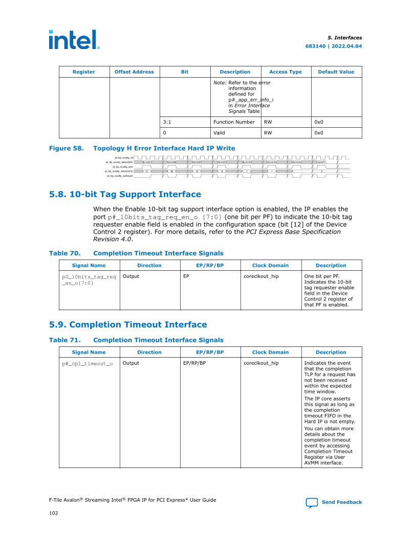
Register Offset Address Bit Description Access Type Default Value
Note: Refer to the errorinformationdefined forp#_app_err_info_iin Error InterfaceSignals Table
3:1 Function Number RW 0x0
0 Valid RW 0x0
Figure 58. Topology H Error Interface Hard IP Writep0_hip_reconfig_clk
p0_hip_reconfig_address[20:0]
p0_hip_reconfig_write
p0_hip_reconfig_writedata[7:0]
p0_hip_reconfig_waitrequest
C5 DB CD 3E 7 1 0
0x1430C 0x1430D 0x1430E 0x1430F 0x14314 0x14315 0x14316 0x14317
5.8. 10-bit Tag Support Interface
When the Enable 10-bit tag support interface option is enabled, the IP enables theport p#_10bits_tag_req_en_o [7:0] (one bit per PF) to indicate the 10-bit tagrequester enable field is enabled in the configuration space (bit [12] of the DeviceControl 2 register). For more details, refer to the PCI Express Base SpecificationRevision 4.0.
Table 70. Completion Timeout Interface Signals
Signal Name Direction EP/RP/BP Clock Domain Description
p0_10bits_tag_req_en_o[7:0]
Output EP coreclkout_hip One bit per PF.Indicates the 10-bittag requester enablefield in the DeviceControl 2 register ofthat PF is enabled.
5.9. Completion Timeout Interface
Table 71. Completion Timeout Interface Signals
Signal Name Direction EP/RP/BP Clock Domain Description
p#_cpl_timeout_o Output EP/RP/BP coreclkout_hip Indicates the eventthat the completionTLP for a request hasnot been receivedwithin the expectedtime window.The IP core assertsthis signal as long asthe completiontimeout FIFO in theHard IP is not empty.You can obtain moredetails about thecompletion timeoutevent by accessingCompletion TimeoutRegister via UserAVMM interface.
5. Interfaces
683140 | 2022.04.04
F-Tile Avalon® Streaming Intel® FPGA IP for PCI Express* User Guide Send Feedback
102
5.10. Power Management Interface
Table 72. Power Management Interface Signals
Signal Name Direction EP/RP/BP Clock Domain Description
p#_pm_state_o[2:0]
Output EP/RP/BP coreclkout_hip /Async Indicates the currentpower state.• 000b : L0 or IDLE• 001b : L0s• 010b : L1• 011b : L2• 100b : L3Note: For 1 x4
Configurationor Topology H,this output willbe async touser clock. It’srecommendedto user tosample thisoutput bus afew times toobtain validvalue.
p#_pm_dstate_o[c*4-1:0]
Output EP/RP/BP Async Power managementD-state for eachfunction.• 0001b : D0• 1000b : D3• Others :
uninitialized orinvalid
Note: This output isasync to userclock. It’srecommendedto user tosample thisoutput bus afew times toobtain validvalue. Theremay be invalidcycles inbetween thetransition oftwo validstates.
Each PF uses fourconsecutive bits. Forexample,pm_dstate_o[3:0]corresponds to PF0,pm_dstate_o[7:4]corresponds to PF1,and so on.For 1 x4 Configurationor Topology H, onlylower 16 bits arevalid.
continued...
5. Interfaces
683140 | 2022.04.04
Send Feedback F-Tile Avalon® Streaming Intel® FPGA IP for PCI Express* User Guide
103
Signal Name Direction EP/RP/BP Clock Domain Description
p#_apps_pm_xmt_pme_i[7:0]
Input EP/BP coreclkout_hip Note: Not availablefor p2 and p3.
The application logicasserts this signal forone cycle to wake upthe PowerManagementCapability (PMC) statemachine from a D1,D2, or D3 powerstate. Upon wake-up,the IP core sends aPM_PME message.Forexample,apps_pm_xmt_pme_i[0] is forPF0,apps_pm_xmt_pme_i[1] is for PF1,and so on.For 1 x4 Configurationor Topology H, onlylower 4 bits are valid.
p#_app_init_rst_i Input RP/BP coreclkout_hip The Application Layeruses this signal torequest a hot reset todownstream devices.The hot reset requestwill be sent when asingle-cycle pulse isapplied to this pin.
p#_surprise_down_err_o
Output EP/RP/BP Async Indicates that asurprise down event isoccurring in thecontroller.
p#_app_req_retry_en_i[x:0]
Input EP Async Note:x=7 for port0and port 1.When asserted, PCIeController will respondto Configuration TLPswith a CRS (ConfigRetry Status) if it hasnot already respondedto a Configuration TLPwith non-CRS statussince the last reset.You can use this tohold off onenumeration.p0_app_req_retry_en_i signal must betied tie to zero whenenabling CvP. For port2 and port 3 whichsupported RP modeonly, this input will notbe used.For 1 x4 Configurationor Topology H, onlylower 4 bits are valid.Each bit correspondsto a PF. For example,app_req_retry_en_i[0] is for PF0,
continued...
5. Interfaces
683140 | 2022.04.04
F-Tile Avalon® Streaming Intel® FPGA IP for PCI Express* User Guide Send Feedback
104

Signal Name Direction EP/RP/BP Clock Domain Description
app_req_retry_en_i[1] is for PF1, andso on.
p#_sys_aux_pwr_det_i
Input EP/BP coreclkout_hip Auxiliary PowerDetected. Used toreport to the hostsoftware that auxiliarypower (Vaux) ispresent. Refer to theDevice Status Registerin the PCI ExpressCapability Structure.Assertion of this signalwill put the device intoL2 link state instead ofL3 link state after L23Ready state. Tie thissignal to “0” when notused.
p#_app_ready_entr_l23_i
Input EP/BP coreclkout_hip The application logicasserts this signal toindicate that it isready to enter theL2/L3 Ready state. Theapp_ready_entr_l23_isignal is provided forapplications that mustcontrol the L2/L3Ready entry (in casecertain tasks must beperformed beforegoing into L2/L3Ready).The core delayssending PM_Enter_L23(in response toPM_Turn_Off) untilthis signal becomesactive.It must be keptasserted until L2 entryhas completed.This is a level-sensitive signal.
p#_apps_pm_xmt_turnoff_i
Input RP coreclkout_hip This signal is arequest from theApplication Layer togenerate aPM_Turn_Offmessage.The Application Layermust assert this signalfor one clock cycle.The IP core does notreturn anacknowledgement orgrant signal.The Application Layermust not pulse thesame signal again
continued...
5. Interfaces
683140 | 2022.04.04
Send Feedback F-Tile Avalon® Streaming Intel® FPGA IP for PCI Express* User Guide
105
Signal Name Direction EP/RP/BP Clock Domain Description
until the previousmessage has beentransmitted.
p#_app_xfer_pending_i
Input EP/BP coreclkout_hip This signal is onlyvalid during L1 state,it is only used to bringdevice to exit L1 andback to L0 whenasserted. It cannotprevent device toenter L1. PowerStatefield of PowerManagement Controland Status Registertake higherprecedence than thissignal. It triggers L1exit but the linktransits back to L1again from L0 if theD3 state is notcleared.This is a level-sensitive signal.
5.11. Hot Plug Interface (RP Only)
Table 73. Hot Plug Interface Signals
Signal Name Direction EP/RP/BP Clock Domain Description
p#_sys_atten_button_pressed_i
Input RP coreclkout_hip Attention ButtonPressed. Indicatesthat the systemattention button waspressed, and sets theAttention ButtonPressed bit in the SlotStatus Register.
p#_sys_pwr_fault_det_i
Input RP coreclkout_hip Power Fault Detected.Indicates the powercontroller detected apower fault at thisslot.
p#_sys_mrl_sensor_chged_i
Input RP coreclkout_hip MRL Sensor Changed.Indicates that thestate of the MRLsensor has changed.
p#_sys_pre_det_chged_i
Input RP coreclkout_hip Presence DetectChanged. Indicatesthat the state of thecard presencedetector has changed.
p#_sys_cmd_cpled_int_i
Input RP coreclkout_hip Command CompletedInterrupt. Indicatesthat the Hot Plugcontroller completed acommand.
continued...
5. Interfaces
683140 | 2022.04.04
F-Tile Avalon® Streaming Intel® FPGA IP for PCI Express* User Guide Send Feedback
106
Signal Name Direction EP/RP/BP Clock Domain Description
p#_sys_pre_det_state_i
Input RP coreclkout_hip Indicates whether ornot a card is presentin the slot.0 : slot is empty.1 : card is present inthe slot.
p#_sys_mrl_sensor_state_i
Input RP coreclkout_hip MRL Sensor State.Indicates the state ofthe manually operatedretention latch (MRL)sensor.0 : MRL is closed.1 : MRL is open.
p#_sys_eml_interlock_engaged_i
Input RP coreclkout_hip Indicates whether thesystemelectromechanicalinterlock is engaged,and controls the stateof theelectromechanicalinterlock status bit inthe Slot StatusRegister.
5.12. Configuration Output Interface
The Transaction Layer configuration output (tl_cfg) bus provides a subset of theinformation stored in the Configuration Space. Use this information in conjunction withthe app_err* signals to understand TLP transmission problems.
Table 74. Configuration Output Interface Signals
Signal Name Direction EP/RP/BP Clock Domain Description
p#_tl_cfg_ctl_o[15:0]
Output EP/RP/BP coreclkout_hip Multiplexed dataoutput from theregister specified bytl_cfg_add_o[4:0].The detailedinformation for eachfield in this bus isdefined inConfiguration OutputInterface (COI).
p#_tl_cfg_add_o[4:0]
Output EP/RP/BP coreclkout_hip This address buscontains the indexindicating whichConfiguration Spaceregister information isbeing driven onto thetl_cfg_ctl_o[15:0]bits.
p#_tl_cfg_func_o[2:0]
Output EP/RP/BP coreclkout_hip Note: Not availablefor p2 and p3.
Specifies the functionwhose ConfigurationSpace register valuesare being driven outon tl_cfg_ctl_o[15:0].
continued...
5. Interfaces
683140 | 2022.04.04
Send Feedback F-Tile Avalon® Streaming Intel® FPGA IP for PCI Express* User Guide
107
Signal Name Direction EP/RP/BP Clock Domain Description
• 3'b000: PhysicalFunction 0 (PF0)
• 3'b001: PF1and soon
p#_dl_timer_update_o
Output EP/RP/BP coreclkout_hip Active high pulse thatasserts whenever thecurrent link speed,link width, or maxpayload size changes.When any of theseparameters changes,the IP's internalReplay/ACK-NAKtimers default back totheir internallycalculated PCIe tables.To override thesedefault values,reprogram the PortLogic register whenthese events occur.
5.13. Configuration Intercept Interface (EP Only)
Table 75. Configuration Intercept Interface Signals
Signal Name Direction EP/RP/BP Clock Domain Description
p#_cii_req_o Output EP coreclkout_hip Note: Not available forp2 and p3.Indicates the CFGrequest is interceptedand all the other CIIsignals are valid.
p#_cii_hdr_poisoned_o
Output EP coreclkout_hip Note: Not available forp2 and p3.The poisoned bit inthe received TLPheader on the CII.
p#_cii_hdr_first_be_o[3:0]
Output EP coreclkout_hip Note: Not available forp2 and p3.The first dword byteenable field in thereceived TLP headeron the CII.
p#_cii_func_num_o[2:0]
Output EP coreclkout_hip Note: Not available forp2 and p3.The function numberin the received TLPheader on the CII.Applicable whenmultiple PhysicalFunctions are enabled
p#_cii_wr_o Output EP coreclkout_hip Note: Not available forp2 and p3.Indicates thatcii_dout_o is valid.This signal is asserted
continued...
5. Interfaces
683140 | 2022.04.04
F-Tile Avalon® Streaming Intel® FPGA IP for PCI Express* User Guide Send Feedback
108
Signal Name Direction EP/RP/BP Clock Domain Description
only for aconfiguration writerequest.
p#_cii_addr_o[9:0]
Output EP coreclkout_hip Note: Not available forp2 and p3.The double wordregister address in thereceived TLP headeron the CII.
p#_cii_dout_o[31:0]
Output EP coreclkout_hip Note: Not available forp2 and p3.Received TLP payloaddata from the linkpartner to yourapplication client. Thedata is in little endianformat. The firstreceived payload byteis in [7:0].
p#_cii_override_en_i
Input EP coreclkout_hip Note: Not available forp2 and p3.Override enable.When the applicationlogic asserts thisinput, the PCIe HardIP overrides the CfgWrpayload or CfgRdcompletion using thedata supplied by theapplication logic oncii_override_din.
p#_cii_override_din_i[31:0]
Input EP coreclkout_hip Note: Not available forp2 and p3.
Override data.• CfgWr: override
the write data tothe PCIe Hard IPregister with datasupplied by theapplication logic oncii_override_din.
• CfgRd: overridethe data payload ofthe completion TLPwith data suppliedby the applicationlogic oncii_override_din.
p#_cii_halt_i Input EP coreclkout_hip Note: Not available forp2 and p3.Flow control inputsignal. When cii_halt_iis asserted, the PCIeHard IP halts theprocessing of CFGrequests for the PCIeconfiguration spaceregisters.
p#_cii_wr_vf_active_o
Output EP coreclkout_hip Note: Not available forp2 and p3.
continued...
5. Interfaces
683140 | 2022.04.04
Send Feedback F-Tile Avalon® Streaming Intel® FPGA IP for PCI Express* User Guide
109
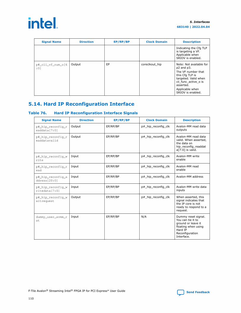
Signal Name Direction EP/RP/BP Clock Domain Description
Indicating the Cfg TLPis targeting a VF.Applicable whenSRIOV is enabled.
p#_cii_vf_num_o[6:0]
Output EP coreclkout_hip Note: Not available forp2 and p3.The VF number thatthis Cfg TLP istargeted. Valid whencii_func_active_o isasserted.Applicable whenSRIOV is enabled.
5.14. Hard IP Reconfiguration Interface
Table 76. Hard IP Reconfiguration Interface Signals
Signal Name Direction EP/RP/BP Clock Domain Description
p#_hip_reconfig_readdata[7:0]
Output EP/RP/BP p#_hip_reconfig_clk Avalon-MM read dataoutputs
p#_hip_reconfig_readdatavalid
Output EP/RP/BP p#_hip_reconfig_clk Avalon-MM read datavalid. When asserted,the data onhip_reconfig_readdata[7:0] is valid.
p#_hip_reconfig_write
Input EP/RP/BP p#_hip_reconfig_clk Avalon-MM writeenable
p#_hip_reconfig_read
Input EP/RP/BP p#_hip_reconfig_clk Avalon-MM readenable
p#_hip_reconfig_address[20:0]
Input EP/RP/BP p#_hip_reconfig_clk Avalon-MM address
p#_hip_reconfig_writedata[7:0]
Input EP/RP/BP p#_hip_reconfig_clk Avalon-MM write datainputs
p#_hip_reconfig_waitrequest
Output EP/RP/BP p#_hip_reconfig_clk When asserted, thissignal indicates thatthe IP core is notready to respond to arequest.
dummy_user_avmm_rst
Input EP/RP/BP N/A Dummy reset signal.You can tie it toground or leave itfloating when usingHard IPReconfigurationInterface.
5. Interfaces
683140 | 2022.04.04
F-Tile Avalon® Streaming Intel® FPGA IP for PCI Express* User Guide Send Feedback
110
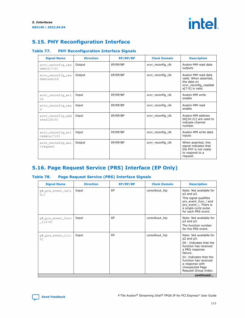
5.15. PHY Reconfiguration Interface
Table 77. PHY Reconfiguration Interface Signals
Signal Name Direction EP/RP/BP Clock Domain Description
xcvr_reconfig_readdata[7:0]
Output EP/RP/BP xcvr_reconfig_clk Avalon-MM read dataoutputs
xcvr_reconfig_readdatavalid
Output EP/RP/BP xcvr_reconfig_clk Avalon-MM read datavalid. When asserted,the data onxcvr_reconfig_readdata[7:0] is valid.
xcvr_reconfig_write
Input EP/RP/BP xcvr_reconfig_clk Avalon-MM writeenable
xcvr_reconfig_read
Input EP/RP/BP xcvr_reconfig_clk Avalon-MM readenable
xcvr_reconfig_address[24:0]
Input EP/RP/BP xcvr_reconfig_clk Avalon-MM addressbit[24:21] are used toindicate channelnumber.
xcvr_reconfig_writedata[7:0]
Input EP/RP/BP xcvr_reconfig_clk Avalon-MM write datainputs
xcvr_reconfig_waitrequest
Output EP/RP/BP xcvr_reconfig_clk When asserted, thissignal indicates thatthe PHY is not readyto respond to arequest.
5.16. Page Request Service (PRS) Interface (EP Only)
Table 78. Page Request Service (PRS) Interface Signals
Signal Name Direction EP/RP/BP Clock Domain Description
p#_prs_event_valid_i
Input EP coreclkout_hip Note: Not available forp2 and p3.This signal qualifiesprs_event_func_i andprs_event_i. There isa single-cycle pulsefor each PRS event.
p#_prs_event_func_i[2:0]
Input EP coreclkout_hip Note: Not available forp2 and p3.The function numberfor the PRS event.
p#_prs_event_i[1:0]
Input EP coreclkout_hip Note: Not available forp2 and p3.00 : Indicates that thefunction has receiveda PRG responsefailure.01: Indicates that thefunction has receiveda response withUnexpected PageRequest Group Index.
continued...
5. Interfaces
683140 | 2022.04.04
Send Feedback F-Tile Avalon® Streaming Intel® FPGA IP for PCI Express* User Guide
111
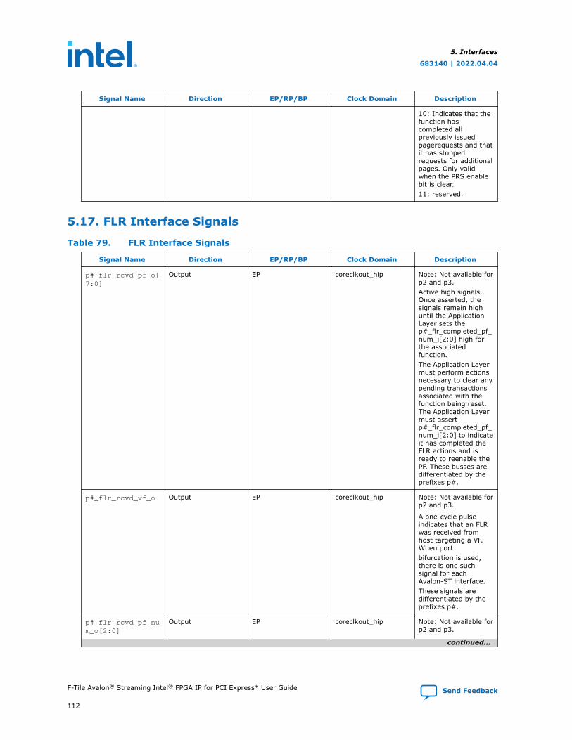
Signal Name Direction EP/RP/BP Clock Domain Description
10: Indicates that thefunction hascompleted allpreviously issuedpagerequests and thatit has stoppedrequests for additionalpages. Only validwhen the PRS enablebit is clear.11: reserved.
5.17. FLR Interface Signals
Table 79. FLR Interface Signals
Signal Name Direction EP/RP/BP Clock Domain Description
p#_flr_rcvd_pf_o[7:0]
Output EP coreclkout_hip Note: Not available forp2 and p3.Active high signals.Once asserted, thesignals remain highuntil the ApplicationLayer sets thep#_flr_completed_pf_num_i[2:0] high forthe associatedfunction.The Application Layermust perform actionsnecessary to clear anypending transactionsassociated with thefunction being reset.The Application Layermust assertp#_flr_completed_pf_num_i[2:0] to indicateit has completed theFLR actions and isready to reenable thePF. These busses aredifferentiated by theprefixes p#.
p#_flr_rcvd_vf_o Output EP coreclkout_hip Note: Not available forp2 and p3.
A one-cycle pulseindicates that an FLRwas received fromhost targeting a VF.When portbifurcation is used,there is one suchsignal for eachAvalon-ST interface.These signals aredifferentiated by theprefixes p#.
p#_flr_rcvd_pf_num_o[2:0]
Output EP coreclkout_hip Note: Not available forp2 and p3.
continued...
5. Interfaces
683140 | 2022.04.04
F-Tile Avalon® Streaming Intel® FPGA IP for PCI Express* User Guide Send Feedback
112
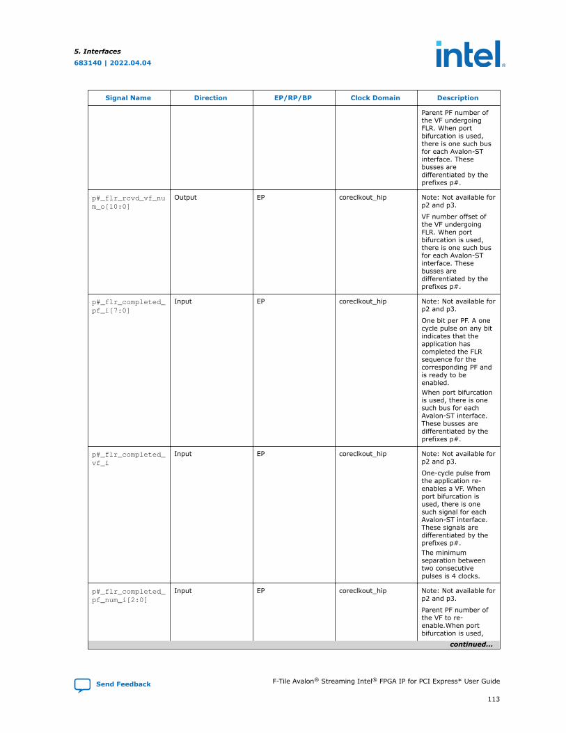
Signal Name Direction EP/RP/BP Clock Domain Description
Parent PF number ofthe VF undergoingFLR. When portbifurcation is used,there is one such busfor each Avalon-STinterface. Thesebusses aredifferentiated by theprefixes p#.
p#_flr_rcvd_vf_num_o[10:0]
Output EP coreclkout_hip Note: Not available forp2 and p3.
VF number offset ofthe VF undergoingFLR. When portbifurcation is used,there is one such busfor each Avalon-STinterface. Thesebusses aredifferentiated by theprefixes p#.
p#_flr_completed_pf_i[7:0]
Input EP coreclkout_hip Note: Not available forp2 and p3.
One bit per PF. A onecycle pulse on any bitindicates that theapplication hascompleted the FLRsequence for thecorresponding PF andis ready to beenabled.When port bifurcationis used, there is onesuch bus for eachAvalon-ST interface.These busses aredifferentiated by theprefixes p#.
p#_flr_completed_vf_i
Input EP coreclkout_hip Note: Not available forp2 and p3.
One-cycle pulse fromthe application re-enables a VF. Whenport bifurcation isused, there is onesuch signal for eachAvalon-ST interface.These signals aredifferentiated by theprefixes p#.The minimumseparation betweentwo consecutivepulses is 4 clocks.
p#_flr_completed_pf_num_i[2:0]
Input EP coreclkout_hip Note: Not available forp2 and p3.
Parent PF number ofthe VF to re-enable.When portbifurcation is used,
continued...
5. Interfaces
683140 | 2022.04.04
Send Feedback F-Tile Avalon® Streaming Intel® FPGA IP for PCI Express* User Guide
113
Signal Name Direction EP/RP/BP Clock Domain Description
there is one such busfor each Avalon-STinterface. Thesebusses aredifferentiated by theprefixes p#.
p#_flr_completed_vf_num_i[2:0]
Input EP coreclkout_hip Note: Not available forp2 and p3.VF number offset ofthe VF to re-enable.When portbifurcation is used,there is one such busfor each Avalon-STinterface. Thesebusses aredifferentiated by theprefixes. p#.
5.18. PTM Interface Signals
Table 80. PTM Interface Signals
Signal Name Direction EP/RP/BP Clock Domain Description
ptm_clk_updated_o Output EP coreclkout_hip An active high pulseindicating that theptm_local_clock[63:0]contains the newupdated PTM time/clock.This signal can only beasserted whenptm_context_valid =‘1’.
ptm_local_clock_o[63:0]
Output EP coreclkout_hip Calculated local PTMclock value
ptm_context_valid_o
Output EP coreclkout_hip PTM context validindication.
ptm_manual_update_i
Input EP coreclkout_hip Indicates that thecontroller shouldupdate the PTMRequester Contextand Clock now. This isused when manualPTM context updatemode is selected.This signals remainasserted until newptm_clk_updated_o isasserted. Between twomanual updaterequests, you arerequired to ensure thissignal is deassertedfor at least 32 ns.
5. Interfaces
683140 | 2022.04.04
F-Tile Avalon® Streaming Intel® FPGA IP for PCI Express* User Guide Send Feedback
114
5.19. VF Error Flag Interface Signals
Table 81. VF Error Flag Interface Signals
Signal Name Direction EP/RP/BP Clock Domain Description
p#_vf_err_poisonedwrreq_s0_o
p#_vf_err_poisonedwrreq_s1_o
p#_vf_err_poisonedwrreq_s2_o (p0only)p#_vf_err_poisonedwrreq_s3_o (p0only)
Output EP coreclkout_hip Indicates a PoisonedWrite Request isreceived.
p#_vf_err_poisonedcompl_s0_o
p#_vf_err_poisonedcompl_s1_o
p#_vf_err_poisonedcompl_s2_o (p0only)p#_vf_err_poisonedcompl_s3_o (p0only)
Output EP coreclkout_hip Indicates a PoisonedCompletion isreceived.
p#_vf_err_ur_posted_s0_o
p#_vf_err_ur_posted_s1_o
p#_vf_err_ur_posted _s2_o (p0 only)p#_vf_err_ur_posted _s3_o (p0 only)
Output EP coreclkout_hip Indicates a Posted URrequest is received.
p#_vf_err_ca_postedreq_s0_o
p#_vf_err_ca_postedreq_s1_o
p#_vf_err_ca_postedreq _s2_o (p0only)p#_vf_err_ca_postedreq _s3_o (p0only)
Output EP coreclkout_hip Indicates a Posted CArequest is received.
p#_vf_err_vf_num_s0_o[10:0]
p#_vf_err_vf_num_s1_o[10:0]
p#_vf_err_vf_num_s2_o[10:0] (p0only)p#_vf_err_vf_num_s3_o[10:0] (p0only)
Output EP coreclkout_hip Indicates the VFnumber for which theerror is detected.
continued...
5. Interfaces
683140 | 2022.04.04
Send Feedback F-Tile Avalon® Streaming Intel® FPGA IP for PCI Express* User Guide
115
Signal Name Direction EP/RP/BP Clock Domain Description
p#_vf_err_num_s0_o[2:0]
p#_vf_err_num_s1_o[2:0]
p#_vf_err_num_s2_o[2:0] (p0 only)p#_vf_err_num_s3_o[2:0] (p0 only)
Output EP coreclkout_hip Indicates the physicalfunction numberassociated with the VFthat has the error.
p#_vf_err_overflow_o
Output EP coreclkout_hip Indicates a VF errorFIFO overflow and aloss of an error report.The overflow canhappen whencoreclkout_hip isslower than thedefault value.If coreclkout_hip isrunning at the defaultfrequency, theoverflow will nothappen.
p#_user_sent_vfnonfatalmsg_i
Input EP coreclkout_hip Indicates the userapplication sent anon-fatal errormessage in responseto an error detected.
p#_user_vfnonfatalmsg_vfnum_i[10:0]
Input EP coreclkout_hip Indicates the VFnumber for which theerror message wasgenerated. This bus isvalid whenuser_sent_vfnonfatalmsg_s0_i is high.
p#_user_vfnonfatalmsg_func_num_i[2:0]
Input EP coreclkout_hip Indicates the PFnumber associatedwith the VF with theerror. This bus is validwhenuser_sent_vfnonfatalmsg_s0_i ishigh.
5.20. VirtIO PCI Configuration Access Interface Signals
Table 82. VirtIO PCI Configuration Access Interface Signals
Signal Name Direction EP/RP/BP Clock Domain Description
p#_virtio_pcicfg_vfaccess_o
Output EP coreclkout_hip Indicates the driveraccess is to a VF.The correspondingVirtual Function isidentified from the
continued...
5. Interfaces
683140 | 2022.04.04
F-Tile Avalon® Streaming Intel® FPGA IP for PCI Express* User Guide Send Feedback
116

Signal Name Direction EP/RP/BP Clock Domain Description
value ofvirtio_pcicfg_vfnum_o.
p#_virtio_pcicfg_vfnum_o[VFNUM_WIDTH-1:0]
Output EP coreclkout_hip Indicates thecorresponding VirtualFunction numberassociated with thecurrent PhysicalFunction that thedriver’s write or readaccess is targeting.Validated byvirtio_pcicfg_vfaccess_o and by driver writeaccess topci_cfg_data, or driverread access topci_cfg_data.
p#_virtio_pcicfg_pfnum_o[PFNUM_WIDTH-1:0]
Output EP coreclkout_hip Indicates thecorresponding PhysicalFunction number thatthe driver’s write orread access istargeting.Validated by driverwrite access topci_cfg_data, or driverread access topci_cfg_data.
p#_virtio_pcicfg_bar_o[7:0]
Output EP coreclkout_hip Indicates the BARholding the PCIconfiguration accessstructure. The driversets the BAR to accessby writing to cap.bar.Values 0x0 to 0x5specify a BARbelonging to thefunction locatedbeginning at 10h inthe PCI ConfigurationSpace.The BAR can be either32-bit or 64-bit.Validated by driverwrite access topci_cfg_data, or driverread access topci_cfg_data.The corresponding PFor VF is identified fromthe value ofvirtio_pcicfg_p/vfnum_o.
p#_virtio_pcicfg_length_o[31:0]
Output EP coreclkout_hip Indicates the length ofthe structure. Thelength may includepadding, or fieldsunused by the driver,or future extensions.
continued...
5. Interfaces
683140 | 2022.04.04
Send Feedback F-Tile Avalon® Streaming Intel® FPGA IP for PCI Express* User Guide
117
Signal Name Direction EP/RP/BP Clock Domain Description
The driver sets thesize of the access bywriting 1, 2 or 4 tocap.length.Validated by driverwrite access topci_cfg_data, or driverread access topci_cfg_data.The corresponding PFor VF is identified fromthe value ofvirtio_pcicfg_p/vfnum_o.
p#_virtio_pcicfg_baroffset_o[31:0]
Output EP coreclkout_hip Indicates where thestructure beginsrelative to the baseaddress associatedwith the BAR. Thedriver sets the offsetwithin the BAR bywriting to cap.offset.Validated by driverwrite access topci_cfg_data, or driverread access topci_cfg_data.The corresponding PFor VF is identified fromthe value ofvirtio_pcicfg_p/vfnum_o.
p#_virtio_pcicfg_cfgdata_o[31:0]
Output EP coreclkout_hip Indicates the data forBAR access. Thepci_cfg_data willprovide a window ofsize cap.length intothe given cap.bar atoffset cap.offset.Validated by driverwrite access topci_cfg_data. Thecorresponding PF orVF is identified fromthe value ofvirtio_pcicfg_p/vfnum_o.
p#_virtio_pcicfg_cfgwr_o
Output EP coreclkout_hip Indicates driver writeaccess topci_cfg_data.The corresponding PFor VF is identified fromthe value ofvirtio_pcicfg_p/vfnum_o.
p#_virtio_pcicfg_cfgrd_o
Output EP coreclkout_hip Indicates driver readaccess topci_cfg_data.The corresponding PFor VF is identified fromthe value ofvirtio_pcicfg_p/vfnum_o.
continued...
5. Interfaces
683140 | 2022.04.04
F-Tile Avalon® Streaming Intel® FPGA IP for PCI Express* User Guide Send Feedback
118
Signal Name Direction EP/RP/BP Clock Domain Description
p#_virtio_pcicfg_appvfnum_i[VFNUM_WIDTH-1:0]
Input EP coreclkout_hip This is a dummysignal created forbackwardcompatibility with P-Tile PCIe Hard IP. Itcan be safely ignoredin new design.
p#_virtio_pcicfg_apppfnum_i[PFNUM_WIDTH-1:0]
Input EP coreclkout_hip This is a dummysignal created forbackwardcompatibility with P-Tile PCIe Hard IP. Itcan be safely ignoredin new design.
p#_virtio_pcicfg_rdack_i
Input EP coreclkout_hip Indicates anapplication readaccess data ack tostore the config datain pci_cfg_data. Useris required to assertrdack on every readaccess topci_cfg_data. Thecorresponding VirtualFunction isidentified from thevalue ofvirtio_pcicfg_appvfnum_i.
p#_virtio_pcicfg_rdbe_i[3:0]
Input EP coreclkout_hip Indicates applicationenabled bytes withinvirtio_pcicfg_data_i.Validated byvirtio_pcicfg_rdack_i.The correspondingVirtual Function isidentified from thevalue ofvirtio_pcicfg_appvfnum_i.
p#_virtio_pcicfg_data_i[31:0]
Input EP coreclkout_hip Indicates applicationdata to be stored inPCI ConfigurationAccess data registers.Validated byvirtio_pcicfg_rdack_iandvirtio_pcicfg_rdbe_i.The correspondingVirtual Function isidentified from thevalue ofvirtio_pcicfg_appvfnum_i.
5. Interfaces
683140 | 2022.04.04
Send Feedback F-Tile Avalon® Streaming Intel® FPGA IP for PCI Express* User Guide
119
6. ParametersThis chapter provides a reference for all the parameters that are configurable in theIntel Quartus Prime IP Parameter Editor for the F-Tile Avalon-ST IP for PCIe.
6.1. Top-Level Settings
Table 83. Top-Level Settings
Parameter Value Default Value Description
Hard IP Mode
Gen4 1x16, Interface - 512-bitGen3 1x16, Interface - 512-bitGen4 1x8, Interface - 256-bitGen3 1x8, Interface - 256-bitGen4 2x8, Interface - 256-bitGen3 2x8, Interface - 256-bitGen4 1x4, Interface - 128-bitGen3 1x4, Interface - 128-bitGen4 2x4, Interface - 128-bitGen3 2x4, Interface - 128-bitGen4 4x4, Interface - 128-bitGen3 4x4, Interface - 128-bit
Gen4x16,Interface - 512-bit
Select the following elements:Lane data rate:• Gen3 and Gen4 are supported.Lane width:• x16, x8 and x4 modes support
both Root Port and Endpoint.
Note:
Gen1/Gen2 or lower linkwidth configurations aresupported via link downtraining. Refer to Figure 2for more detail on thesupported configurationmodes
Port Mode
Root PortNative Endpoint
Note:
These are the availableoptions when EnableTLP Bypass is set toFalse. If TLP Bypassmode is enabled, referto the table Port ModeOptions in TLP Bypassbelow for available portmode options.
Native Endpoint Specifies the port type.
Enable PMA registersaccess True/False False Enable the PHY Reconfiguration
Interface.
continued...
683140 | 2022.04.04
Send Feedback
Intel Corporation. All rights reserved. Intel, the Intel logo, and other Intel marks are trademarks of IntelCorporation or its subsidiaries. Intel warrants performance of its FPGA and semiconductor products to currentspecifications in accordance with Intel's standard warranty, but reserves the right to make changes to anyproducts and services at any time without notice. Intel assumes no responsibility or liability arising out of theapplication or use of any information, product, or service described herein except as expressly agreed to inwriting by Intel. Intel customers are advised to obtain the latest version of device specifications before relyingon any published information and before placing orders for products or services.*Other names and brands may be claimed as the property of others.
ISO9001:2015Registered
Parameter Value Default Value Description
PLD Clock Frequency
500 MHz450 MHz400 MHz350 MHz250 MHz
500 MHz (forGen4 modes)250 MHz (forGen3 modes)
Select the frequency of theApplication clock. The optionsavailable vary depending on thesetting of the Hard IP Modeparameter.For Gen4 modes, the availableclock frequencies are 500 MHz /400 MHz / 350 MHz (for IntelAgilex)For Gen3 modes, the availableclock frequency is 250 MHz (forIntel Agilex and Intel Stratix® 10DX).
Enable F-Tile Debug Toolkit True/False False Enable F-Tile Debug Toolkit
Enable TLP- Bypass mode True/False False
Enable the TLP Bypass feature.
Note:
For configurations wheremultiple ports areavailable, it is possible toenable TLP Bypass on aper-port basis.
Enable SRIS Mode True/False FalseEnable the Separate ReferenceClock with Independent SpreadSpectrum Clocking (SRIS) feature.
Enable Independent Perst True/False FalseEnable independent reset of PCSand Controller in User Mode for EP& bypass Upstream mode
Enable CVP (Intel VSEC) True/False False
Enablement of CvP for x16 Coreor Port0, single tile only.p0_app_req_retry_en_i signalmust be tied tie off to zero whenenabling CvP. Refer to Intel AgilexDevice Configuration via Protocol(CvP) Implementation User Guidefor more details on CvP.
Table 84. Port Mode Options in TLP Bypass
ConfigurationAvailable Port Modes
Port 0 Port 1 Port 2 Port 3
1x16 (Gen4x16 orGen3x16)
TLP-Bypass On:Upstream
N/A N/A N/A
TLP-Bypass On:Downstream
N/A N/A N/A
2x8 (Gen4x8/Gen4x8 or Gen3x8/Gen3x8)
TLP-Bypass On:Upstream
TLP-Bypass On:Upstream
N/A N/A
TLP-Bypass On:Downstream
TLP-Bypass On:Downstream
N/A N/A
TLP-Bypass Off:Endpoint
TLP-Bypass On:Upstream
N/A N/A
continued...
6. Parameters
683140 | 2022.04.04
Send Feedback F-Tile Avalon® Streaming Intel® FPGA IP for PCI Express* User Guide
121
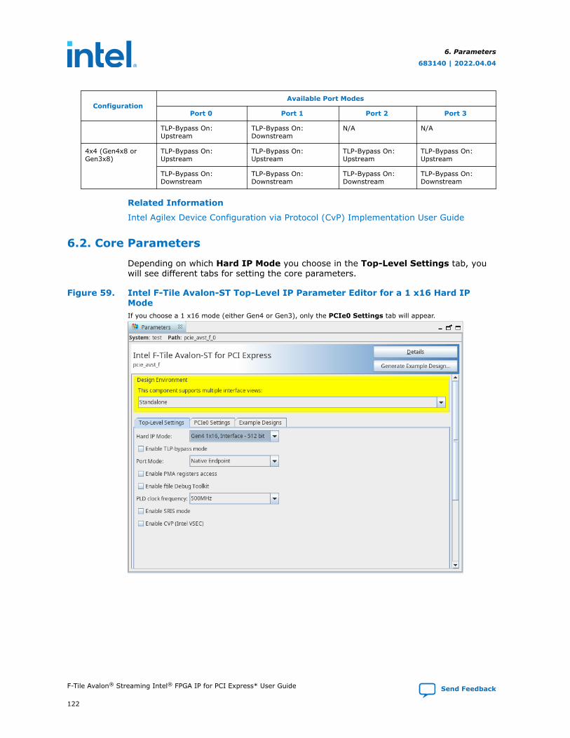
ConfigurationAvailable Port Modes
Port 0 Port 1 Port 2 Port 3
TLP-Bypass On:Upstream
TLP-Bypass On:Downstream
N/A N/A
4x4 (Gen4x8 orGen3x8)
TLP-Bypass On:Upstream
TLP-Bypass On:Upstream
TLP-Bypass On:Upstream
TLP-Bypass On:Upstream
TLP-Bypass On:Downstream
TLP-Bypass On:Downstream
TLP-Bypass On:Downstream
TLP-Bypass On:Downstream
Related Information
Intel Agilex Device Configuration via Protocol (CvP) Implementation User Guide
6.2. Core Parameters
Depending on which Hard IP Mode you choose in the Top-Level Settings tab, youwill see different tabs for setting the core parameters.
Figure 59. Intel F-Tile Avalon-ST Top-Level IP Parameter Editor for a 1 x16 Hard IPModeIf you choose a 1 x16 mode (either Gen4 or Gen3), only the PCIe0 Settings tab will appear.
6. Parameters
683140 | 2022.04.04
F-Tile Avalon® Streaming Intel® FPGA IP for PCI Express* User Guide Send Feedback
122
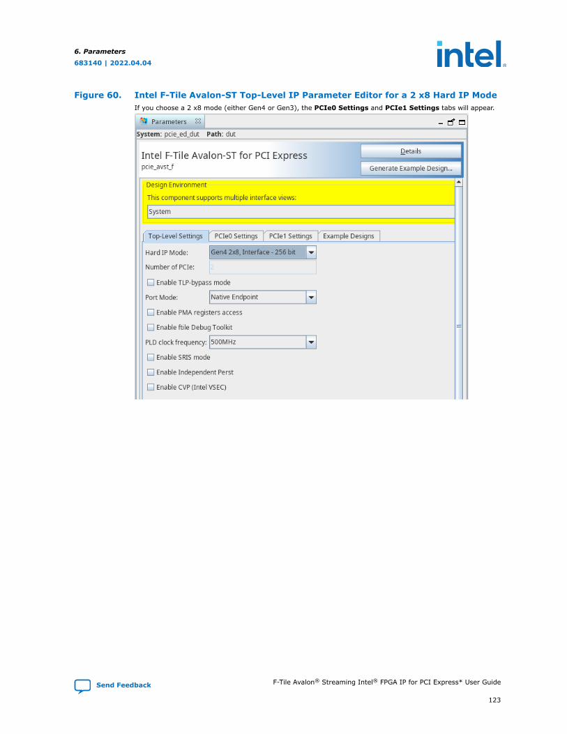
Figure 60. Intel F-Tile Avalon-ST Top-Level IP Parameter Editor for a 2 x8 Hard IP ModeIf you choose a 2 x8 mode (either Gen4 or Gen3), the PCIe0 Settings and PCIe1 Settings tabs will appear.
6. Parameters
683140 | 2022.04.04
Send Feedback F-Tile Avalon® Streaming Intel® FPGA IP for PCI Express* User Guide
123
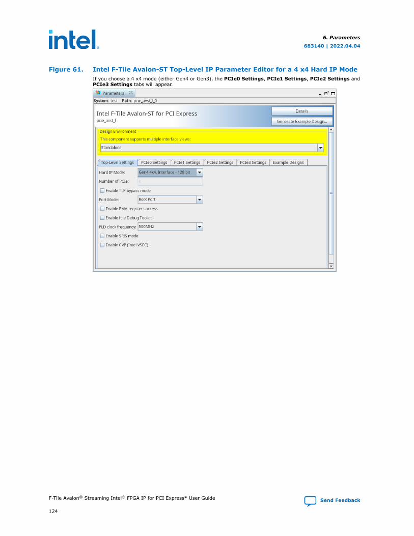
Figure 61. Intel F-Tile Avalon-ST Top-Level IP Parameter Editor for a 4 x4 Hard IP ModeIf you choose a 4 x4 mode (either Gen4 or Gen3), the PCIe0 Settings, PCIe1 Settings, PCIe2 Settings andPCIe3 Settings tabs will appear.
6. Parameters
683140 | 2022.04.04
F-Tile Avalon® Streaming Intel® FPGA IP for PCI Express* User Guide Send Feedback
124
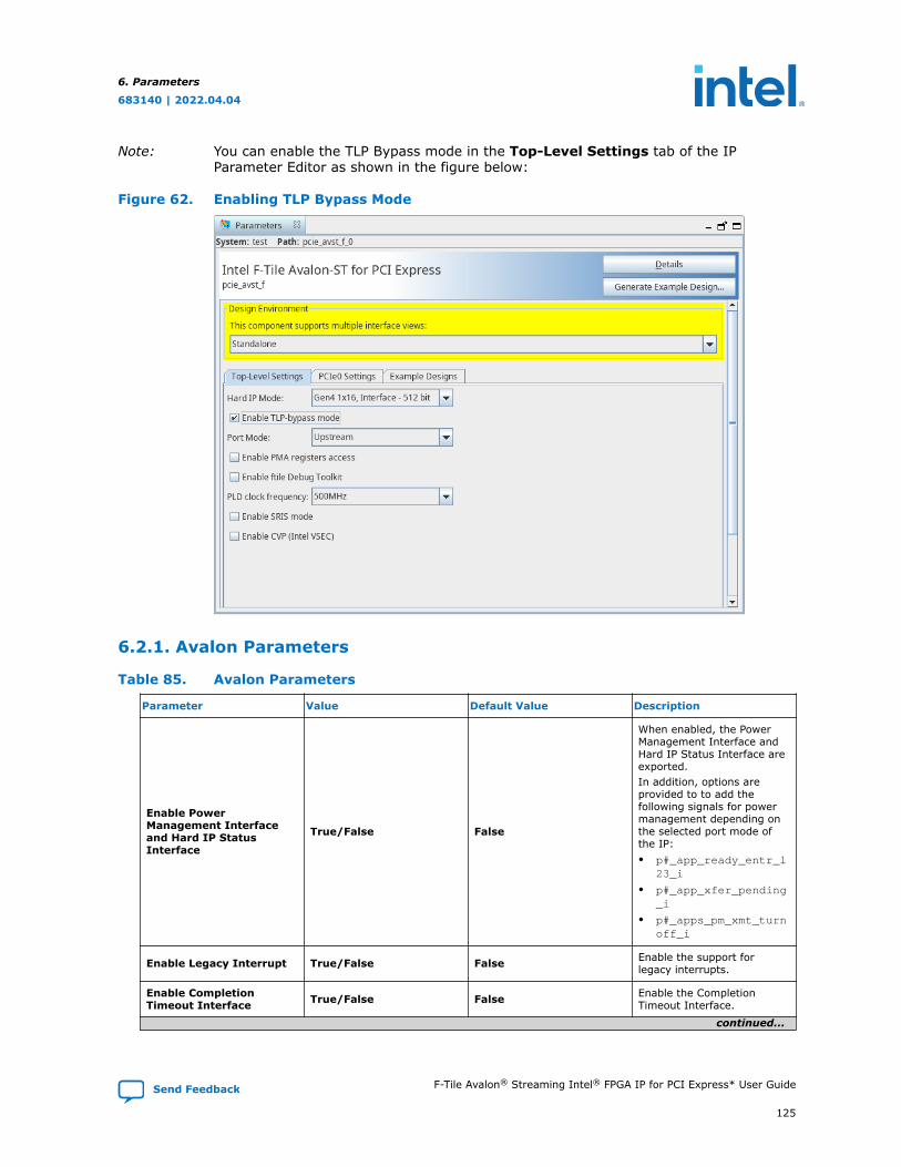
Note: You can enable the TLP Bypass mode in the Top-Level Settings tab of the IPParameter Editor as shown in the figure below:
Figure 62. Enabling TLP Bypass Mode
6.2.1. Avalon Parameters
Table 85. Avalon Parameters
Parameter Value Default Value Description
Enable PowerManagement Interfaceand Hard IP StatusInterface
True/False False
When enabled, the PowerManagement Interface andHard IP Status Interface areexported.In addition, options areprovided to to add thefollowing signals for powermanagement depending onthe selected port mode ofthe IP:• p#_app_ready_entr_l
23_i
• p#_app_xfer_pending_i
• p#_apps_pm_xmt_turnoff_i
Enable Legacy Interrupt True/False False Enable the support forlegacy interrupts.
Enable CompletionTimeout Interface True/False False Enable the Completion
Timeout Interface.
continued...
6. Parameters
683140 | 2022.04.04
Send Feedback F-Tile Avalon® Streaming Intel® FPGA IP for PCI Express* User Guide
125
Parameter Value Default Value Description
Enable ConfigurationIntercept Interface True/False False
Enable the ConfigurationIntercept Interface.
Note: This parameter isonly available in EPmode.
Enable PRS Event True/False False
Enable the Page RequestService (PRS) EventInterface.
Note: This parameter isonly available in EPmode.
Enable Error Interface True/False False Enable the Error Interface.
Enable 10-bit tag supportinterface True/False False
When this parameter isenabled, the 10-bit tagrequester enable signal isenabled as an output portp#_10bits_tag_req_en_o[7:0] (one bit per PF).
Enable Byte Parity Portson Avalon-ST Interface True/False False
When this parameter isenabled, the byte parityports appear on the blocksymbol. These byte parityports include:rx_st_data_par_o,rx_st_hdr_par_o,rx_st_tlp_prfx_par_o,tx_st_data_par_o,tx_st_hdr_par_o, andtx_st_tlp_prfx_par_oports.
6.2.2. Base Address Registers
Table 86. BAR Registers
Parameter Value Description
BAR0 Type
Disabled64-bit prefetchable memory64-bit non-prefetchable memory32-bit non-prefetchable memory
If you select 64-bit prefetchable memory, 2contiguous BARs are combined to form a 64-bitprefetchable BAR; you must set the highernumbered BAR to Disabled.Defining memory as prefetchable allows contiguousdata to be fetched ahead. Prefetching memory isadvantageous when the requestor may requiremore data from the same region than wasoriginally requested. If you specify that a memoryis prefetchable, it must have the following 2attributes:• Reads do not have side effects such as
changing the value of the data read.• Write merging is allowed.
BAR1 TypeDisabled32-bit non-prefetchable memory
For a definition of prefetchable memory, refer tothe BAR0 Type description.
BAR2 Type
Disabled64-bit prefetchable memory64-bit non-prefetchable memory32-bit non-prefetchable memory
For a definition of prefetchable memory and adescription of what happens when you select the64-bit prefetchable memory option, refer to theBAR0 Type description.
continued...
6. Parameters
683140 | 2022.04.04
F-Tile Avalon® Streaming Intel® FPGA IP for PCI Express* User Guide Send Feedback
126
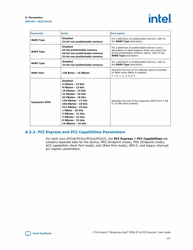
Parameter Value Description
BAR3 TypeDisabled32-bit non-prefetchable memory
For a definition of prefetchable memory, refer tothe BAR0 Type description.
BAR4 Type
Disabled64-bit prefetchable memory64-bit non-prefetchable memory32-bit non-prefetchable memory
For a definition of prefetchable memory and adescription of what happens when you select the64-bit prefetchable memory option, refer to theBAR0 Type description.
BAR5 TypeDisabled32-bit non-prefetchable memory
For a definition of prefetchable memory, refer tothe BAR0 Type description.
BARn Size 128 Bytes - 16 EBytesSpecifies the size of the address space accessibleto BARn when BARn is enabled.n = 0, 1, 2, 3, 4 or 5
Expansion ROM
Disabled4 KBytes - 12 bits8 KBytes - 13 bits16 KBytes - 14 bits32 KBytes - 15 bits64 KBytes - 16 bits128 KBytes - 17 bits256 KBytes - 18 bits512 KBytes - 19 bits1 MByte - 20 bits2 MBytes - 21 bits4 MBytes - 22 bits8 MBytes - 23 bits16 MBytes - 24 bits
Specifies the size of the expansion ROM from 4 KBto 16 MB when enabled.
6.2.3. PCI Express and PCI Capabilities Parameters
For each core (PCIe0/PCIe1/PCIe2/PCIe3), the PCI Express / PCI Capabilities tabcontains separate tabs for the device, PRS (Endpoint mode), MSI (Endpoint mode),ACS capabilities (Root Port mode), slot (Root Port mode), MSI-X, and legacy interruptpin register parameters.
6. Parameters
683140 | 2022.04.04
Send Feedback F-Tile Avalon® Streaming Intel® FPGA IP for PCI Express* User Guide
127
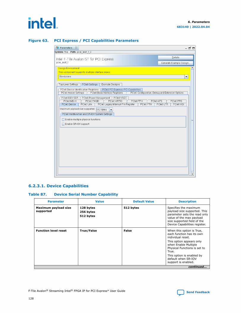
Figure 63. PCI Express / PCI Capabilities Parameters
6.2.3.1. Device Capabilities
Table 87. Device Serial Number Capability
Parameter Value Default Value Description
Maximum payload sizesupported
128 bytes256 bytes512 bytes
512 bytes Specifies the maximumpayload size supported. Thisparameter sets the read onlyvalue of the max payloadsize supported field of theDevice Capabilities register.
Function level reset True/False False When this option is True,each function has its ownindividual reset.This option appears onlywhen Enable MultiplePhysical Functions is set toTrue.This option is enabled bydefault when SR-IOVsupport is enabled.
continued...
6. Parameters
683140 | 2022.04.04
F-Tile Avalon® Streaming Intel® FPGA IP for PCI Express* User Guide Send Feedback
128
Parameter Value Default Value Description
Enable multiple physicalfunctions
True/False False Enables multiple physicalfunctions.
Total physical functions(PFs)
1-8 1 Set the number of physicalfunctions. The IP core cansupport 1 - 8 PFs. Thisparameter is visible only ifEnable multiple physicalfunctions is set to True.Note: 1x4 mode supports
1-4 PFs only.
Enable SR-IOV support True/False False Enable SR-IOV support.
Total virtual functions ofphysical function 0 (PF0VFs)
0-2048 0 Set the number of VFs to beassigned to PhysicalFunction 0. This parameteris visible only if Enable SR-IOV support is set to True.Note: 1x4 mode supports
0-16 only
Total virtual functions ofphysical function 1 (PF1VFs)
0-2048 0 Set the number of VFs to beassigned to PhysicalFunction 1. This parameteris visible only if Enable SR-IOV support is set to Trueand Total physicalfunctions is greater than 1.Note: 1x4 mode supports
0-16 only
Total virtual functions ofphysical function 2 (PF2VFs)
0-2048 0 Set the number of VFs to beassigned to PhysicalFunction 2. This parameteris visible only if Enable SR-IOV support is set to Trueand Total physicalfunctions is greater than 2.Note: 1x4 mode supports
0-16 only
Total virtual functions ofphysical function 3 (PF3VFs)
0-2048 0 Set the number of VFs to beassigned to PhysicalFunction 3. This parameteris visible only if Enable SR-IOV support is set to Trueand Total physicalfunctions is greater than 3.Note: 1x4 mode supports
0-16 only
Total virtual functions ofphysical function 4 (PF4VFs)
0-2048 0 Set the number of VFs to beassigned to PhysicalFunction 4. This parameteris visible only if Enable SR-IOV support is set to Trueand Total physicalfunctions is greater than 4.
Total virtual functions ofphysical function 5 (PF5VFs)
0-2048 0 Set the number of VFs to beassigned to PhysicalFunction 5. This parameteris visible only if Enable SR-
continued...
6. Parameters
683140 | 2022.04.04
Send Feedback F-Tile Avalon® Streaming Intel® FPGA IP for PCI Express* User Guide
129
Parameter Value Default Value Description
IOV support is set to Trueand Total physicalfunctions is greater than 5.
Total virtual functions ofphysical function 6 (PF6VFs)
0-2048 0 Set the number of VFs to beassigned to PhysicalFunction 6. This parameteris visible only if Enable SR-IOV support is set to Trueand Total physicalfunctions is greater than 6.
Total virtual functions ofphysical function 7 (PF7VFs)
0-2048 0 Set the number of VFs to beassigned to PhysicalFunction 7. This parameteris visible only if Enable SR-IOV support is set to Trueand Total physicalfunctions is 8.
6.2.3.2. Link Capabilities
Table 88. Link Capabilities
Parameter Value Default Value Description
Link port number (RootPort only) 0 - 255 1
Sets the read-only value ofthe port number field in theLink Capabilitiesregister. This parameter isfor Root Ports only. It shouldnot be changed.
Slot clock configuration True/False True
When this parameter isTrue, it indicates that theEndpoint uses the samephysical reference clock thatthe system provides on theconnector. When it is False,the IP core uses anindependent clock regardlessof the presence of areference clock on theconnector. This parametersets the Slot ClockConfiguration bit (bit 12) inthe PCI Express LinkStatus register.
6.2.3.3. Legacy Interrupt Pin Register
Table 89. Legacy Interrupts Parameters
Parameter Value Default Value Description
Set Interrupt Pin for PF0 NO INTINTAINTA/INTB/INTC/INTD
NO INT When Legacy Interrupts arenot enabled, the only optionavailable is NO INT.When Legacy Interrupts areenabled and multifunction isdisabled, the only optionavailable is INTA.
6. Parameters
683140 | 2022.04.04
F-Tile Avalon® Streaming Intel® FPGA IP for PCI Express* User Guide Send Feedback
130
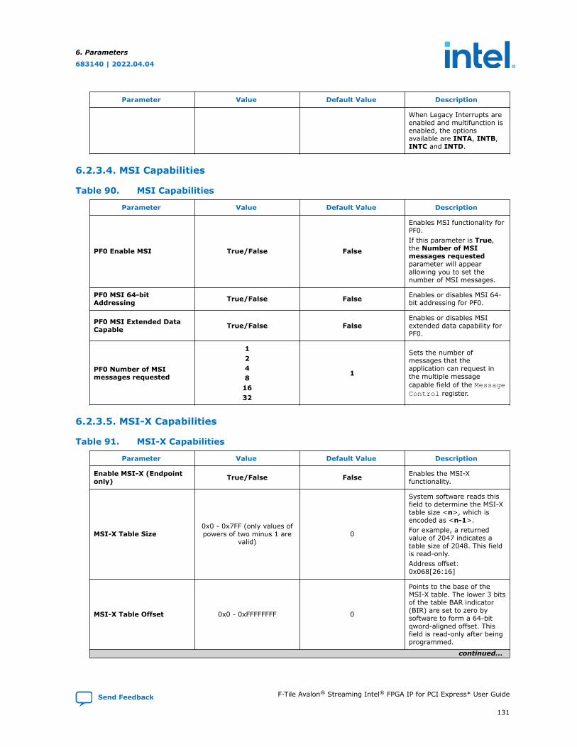
Parameter Value Default Value Description
When Legacy Interrupts areenabled and multifunction isenabled, the optionsavailable are INTA, INTB,INTC and INTD.
6.2.3.4. MSI Capabilities
Table 90. MSI Capabilities
Parameter Value Default Value Description
PF0 Enable MSI True/False False
Enables MSI functionality forPF0.If this parameter is True,the Number of MSImessages requestedparameter will appearallowing you to set thenumber of MSI messages.
PF0 MSI 64-bitAddressing True/False False Enables or disables MSI 64-
bit addressing for PF0.
PF0 MSI Extended DataCapable True/False False
Enables or disables MSIextended data capability forPF0.
PF0 Number of MSImessages requested
1248
1632
1
Sets the number ofmessages that theapplication can request inthe multiple messagecapable field of the MessageControl register.
6.2.3.5. MSI-X Capabilities
Table 91. MSI-X Capabilities
Parameter Value Default Value Description
Enable MSI-X (Endpointonly) True/False False Enables the MSI-X
functionality.
MSI-X Table Size0x0 - 0x7FF (only values ofpowers of two minus 1 are
valid)0
System software reads thisfield to determine the MSI-Xtable size <n>, which isencoded as <n-1>.For example, a returnedvalue of 2047 indicates atable size of 2048. This fieldis read-only.Address offset:0x068[26:16]
MSI-X Table Offset 0x0 - 0xFFFFFFFF 0
Points to the base of theMSI-X table. The lower 3 bitsof the table BAR indicator(BIR) are set to zero bysoftware to form a 64-bitqword-aligned offset. Thisfield is read-only after beingprogrammed.
continued...
6. Parameters
683140 | 2022.04.04
Send Feedback F-Tile Avalon® Streaming Intel® FPGA IP for PCI Express* User Guide
131
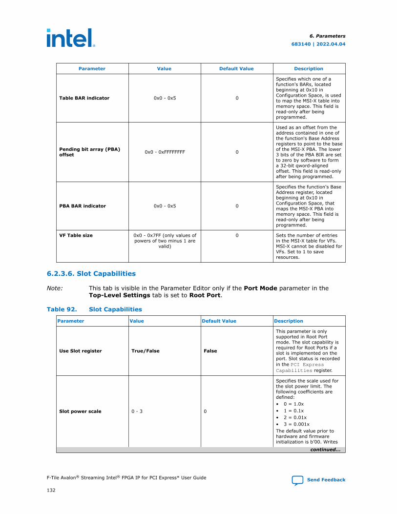
Parameter Value Default Value Description
Table BAR indicator 0x0 - 0x5 0
Specifies which one of afunction's BARs, locatedbeginning at 0x10 inConfiguration Space, is usedto map the MSI-X table intomemory space. This field isread-only after beingprogrammed.
Pending bit array (PBA)offset 0x0 - 0xFFFFFFFF 0
Used as an offset from theaddress contained in one ofthe function's Base Addressregisters to point to the baseof the MSI-X PBA. The lower3 bits of the PBA BIR are setto zero by software to forma 32-bit qword-alignedoffset. This field is read-onlyafter being programmed.
PBA BAR indicator 0x0 - 0x5 0
Specifies the function's BaseAddress register, locatedbeginning at 0x10 inConfiguration Space, thatmaps the MSI-X PBA intomemory space. This field isread-only after beingprogrammed.
VF Table size 0x0 - 0x7FF (only values ofpowers of two minus 1 are
valid)
0 Sets the number of entriesin the MSI-X table for VFs.MSI-X cannot be disabled forVFs. Set to 1 to saveresources.
6.2.3.6. Slot Capabilities
Note: This tab is visible in the Parameter Editor only if the Port Mode parameter in theTop-Level Settings tab is set to Root Port.
Table 92. Slot Capabilities
Parameter Value Default Value Description
Use Slot register True/False False
This parameter is onlysupported in Root Portmode. The slot capability isrequired for Root Ports if aslot is implemented on theport. Slot status is recordedin the PCI ExpressCapabilities register.
Slot power scale 0 - 3 0
Specifies the scale used forthe slot power limit. Thefollowing coefficients aredefined:• 0 = 1.0x• 1 = 0.1x• 2 = 0.01x• 3 = 0.001xThe default value prior tohardware and firmwareinitialization is b’00. Writes
continued...
6. Parameters
683140 | 2022.04.04
F-Tile Avalon® Streaming Intel® FPGA IP for PCI Express* User Guide Send Feedback
132
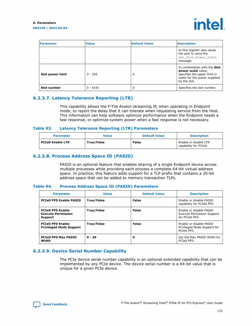
Parameter Value Default Value Description
to this register also causethe port to send theSet_Slot_Power_Limitmessage.
Slot power limit 0 - 255 0
In combination with the Slotpower scale value,specifies the upper limit inwatts for the power suppliedby the slot.
Slot number 0 - 8191 0 Specifies the slot number.
6.2.3.7. Latency Tolerance Reporting (LTR)
This capability allows the F-Tile Avalon streaming IP, when operating in Endpointmode, to report the delay that it can tolerate when requesting service from the Host.This information can help software optimize performance when the Endpoint needs afast response, or optimize system power when a fast response is not necessary.
Table 93. Latency Tolerance Reporting (LTR) Parameters
Parameter Value Default Value Description
PCIe0 Enable LTR True/False False Enable or disable LTRcapability for PCIe0.
6.2.3.8. Process Address Space ID (PASID)
PASID is an optional feature that enables sharing of a single Endpoint device acrossmultiple processes while providing each process a complete 64-bit virtual addressspace. In practice, this feature adds support for a TLP prefix that contains a 20-bitaddress space that can be added to memory transaction TLPs.
Table 94. Process Address Space ID (PASID) Parameters
Parameter Value Default Value Description
PCIe0 PF0 Enable PASID True/False False Enable or disable PASIDcapability for PCIe0 PF0.
PCIe0 PF0 EnableExecute PermissionSupport
True/False False Enable or disable PASIDExecute Permission Supportfor PCIe0 PF0.
PCIe0 PF0 EnablePrivileged Mode Support
True/False False Enable or disable PASIDPrivileged Mode Support forPCIe0 PF0.
PCIe0 PF0 Max PASIDWidth
0 - 20 0 Set the Max PASID Width forPCIe0 PF0.
6.2.3.9. Device Serial Number Capability
The PCIe device serial number capability is an optional extended capability that can beimplemented by any PCIe device. The device serial number is a 64-bit value that isunique for a given PCIe device.
6. Parameters
683140 | 2022.04.04
Send Feedback F-Tile Avalon® Streaming Intel® FPGA IP for PCI Express* User Guide
133
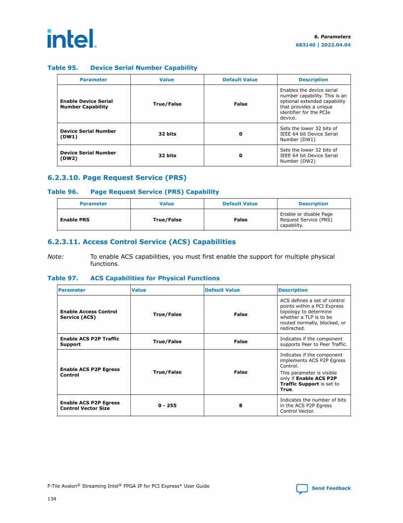
Table 95. Device Serial Number Capability
Parameter Value Default Value Description
Enable Device SerialNumber Capability True/False False
Enables the device serialnumber capability. This is anoptional extended capabilitythat provides a uniqueidentifier for the PCIedevice.
Device Serial Number(DW1) 32 bits 0
Sets the lower 32 bits ofIEEE 64 bit Device SerialNumber (DW1)
Device Serial Number(DW2) 32 bits 0
Sets the lower 32 bits ofIEEE 64 bit Device SerialNumber (DW2)
6.2.3.10. Page Request Service (PRS)
Table 96. Page Request Service (PRS) Capability
Parameter Value Default Value Description
Enable PRS True/False FalseEnable or disable PageRequest Service (PRS)capability.
6.2.3.11. Access Control Service (ACS) Capabilities
Note: To enable ACS capabilities, you must first enable the support for multiple physicalfunctions.
Table 97. ACS Capabilities for Physical Functions
Parameter Value Default Value Description
Enable Access ControlService (ACS) True/False False
ACS defines a set of controlpoints within a PCI Expresstopology to determinewhether a TLP is to berouted normally, blocked, orredirected.
Enable ACS P2P TrafficSupport True/False False Indicates if the component
supports Peer to Peer Traffic.
Enable ACS P2P EgressControl True/False False
Indicates if the componentimplements ACS P2P EgressControl.This parameter is visibleonly if Enable ACS P2PTraffic Support is set toTrue.
Enable ACS P2P EgressControl Vector Size 0 - 255 8
Indicates the number of bitsin the ACS P2P EgressControl Vector.
6. Parameters
683140 | 2022.04.04
F-Tile Avalon® Streaming Intel® FPGA IP for PCI Express* User Guide Send Feedback
134
Table 98. ACS Capabilities for Virtual Functions
Parameter Value Default Value Description
Enable Access ControlService (ACS) True/False False
ACS defines a set of controlpoints within a PCI Expresstopology to determinewhether a TLP is to berouted normally, blocked, orredirected.
6.2.3.12. Power Management
Table 99. Power Management
Parameter Value Default Value Description
Enable L0s acceptablelatency
Maximum of 64 nsMaximum of 128 nsMaximum of 256 nsMaximum of 512 nsMaximum of 1 µsMaximum of 2 µsMaximum of 4 µsNo limit
Maximum of 64 ns
This design parameterspecifies the maximumacceptable latency that theapplication layer can toleratefor any link between thedevice and the root complexto exit the L0s state. It setsthe read-only value of theEndpoint L0s acceptablelatency field of the DeviceCapabilities Register(0x084).This Endpoint does notsupport the L0s or L1 states.However, in a switchedsystem, there may be linksconnected to switches thathave L0s and L1 enabled.This parameter is set toallow system configurationsoftware to read theacceptable latencies for alldevices in the system andthe exit latency for each linkto determine which links canenable Active State PowerManagement (ASPM).This setting is disabled forRoot Ports.The default value of thisparameter is 64 ns. This isthe safest setting for mostdesigns.
Endpoint L1s acceptablelatency
Maximum of 1 µsMaximum of 2 µsMaximum of 4 µsMaximum of 8 µsMaximum of 16 µsMaximum of 32 µsMaximum of 64 µsNo limit
Maximum of 1 µs
This value indicates theacceptable latency that anEndpoint can withstand inthe transition from the L1state to L0 state. It is anindirect measure of theEndpoint’s internal buffering.It sets the read-only value ofthe Endpoint L1 acceptablelatency field of the DeviceCapabilities Register.This Endpoint does notsupport the L0s or L1 states.However, a switched systemmay include links connectedto switches that have L0s
continued...
6. Parameters
683140 | 2022.04.04
Send Feedback F-Tile Avalon® Streaming Intel® FPGA IP for PCI Express* User Guide
135
Parameter Value Default Value Description
and L1 enabled. Thisparameter is set to allowsystem configurationsoftware to read theacceptable latencies for alldevices in the system andthe exit latency for each linkto determine which links canenable Active State PowerManagement (ASPM).This setting is disabled forRoot Ports.
6.2.3.13. Vendor Specific Extended Capability (VSEC) Registers
Table 100. VSEC Register
Parameter Value Default Value Description
Enable CVP (Intel VSEC) True/False False Enables Intel CVP
Vendor Specific ExtendedCapability True/False False Enables the Vendor Specific
Extended Capability (VSEC).
User ID register from theVendor Specific ExtendedCapability
0 - 65534 0
Sets the read-only value ofthe 16-bit User ID registerfrom the Vendor SpecificExtended Capability. Thisparameter is only valid forEndpoints.
Drops Vendor Type0Messages True/False False
When this parameter is setto 1, the IP core dropsvendor Type 0 messageswhile treating them asUnsupported Requests (UR).When it is set to 0, the IPcore passes these messageson to the user logic.This option is not applicablefor TLP Bypass mode. In TLPBypass mode, receivedVendor MSG Type0 willalways be visible on Avalon-ST RX interface.
Drops Vendor Type1Messages True/False False
When this parameter is setto 1, the IP core silentlydrops vendor Type 1messages.When it is set to 0, the IPcore passes these messageson to the user logic.This option is not applicablefor TLP Bypass mode. In TLPBypass mode, receivedVendor MSG Type1 willalways be visible on Avalon-ST RX interface.
6. Parameters
683140 | 2022.04.04
F-Tile Avalon® Streaming Intel® FPGA IP for PCI Express* User Guide Send Feedback
136
6.2.3.14. Precision Time Measurement (PTM)
Table 101. Precision Time Measurement (PTM) Parameters
Parameter Value Default Value Description
Enable PTM True/False False When selected, PrecisionTime Management (PTM)Capability is available forPCIe0. Refers to User Guidefor details on PTMoperations.
Period between eachautomatic update of PTMcontent (in ms)
Disable12345678910
Disable Determines the PTM contextauto-update internal. Byselecting 'Disable', itprevents PTM context auto-update.
6.2.3.15. Address Translation Services (ATS)
Table 102.
Parameter Value Default Value Description
Enable AddressTranslation Services(ATS)
True/False False Enable or disable AddressTranslation Services (ATS)capability.When ATS is enabled,senders can request andcache translated addressesusing the RP memory spacefor later use.
6.2.3.16. TLP Processing Hints (TPH)
Table 103.
Parameter Value Default Value Description
Enable TLP ProcessingHints (TPH)
True/False False Enable or disable TLPProcessing Hints (TPH)capability.Using TPH may improvelatency and trafficcongestion.
Interrupt mode True/False False When set, steering tag isselected by an MSI-Xinterrupt vector number
Device specific mode True/False False Select the steering tag mode
Steering Tag tablelocation
ST table not presentMSI-X table
ST table not present Select the steering tag tablelocation
Steering Tag table size 0-2047 0 Sets the steering tag tablesize
6. Parameters
683140 | 2022.04.04
Send Feedback F-Tile Avalon® Streaming Intel® FPGA IP for PCI Express* User Guide
137
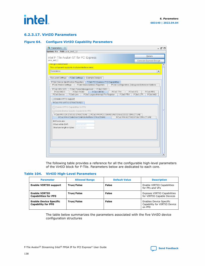
6.2.3.17. VirtIO Parameters
Figure 64. Configure VirtIO Capability Parameters
The following table provides a reference for all the configurable high-level parametersof the VirtIO block for F-Tile. Parameters below are dedicated to each core.
Table 104. VirtIO High-Level Parameters
Parameter Allowed Range Default Value Description
Enable VIRTIO support True/False False Enable VIRTIO Capabilitiesfor PFs and VFs
Enable VIRTIOCapabilities for PF0
True/False False Exposes VIRTIO Capabilitiesfor VIRTIO Capable Devices
Enable Device SpecificCapability for PF0
True/False False Enables Device SpecificCapability for VIRTIO Deviceon PF0
The table below summarizes the parameters associated with the five VirtIO deviceconfiguration structures
6. Parameters
683140 | 2022.04.04
F-Tile Avalon® Streaming Intel® FPGA IP for PCI Express* User Guide Send Feedback
138
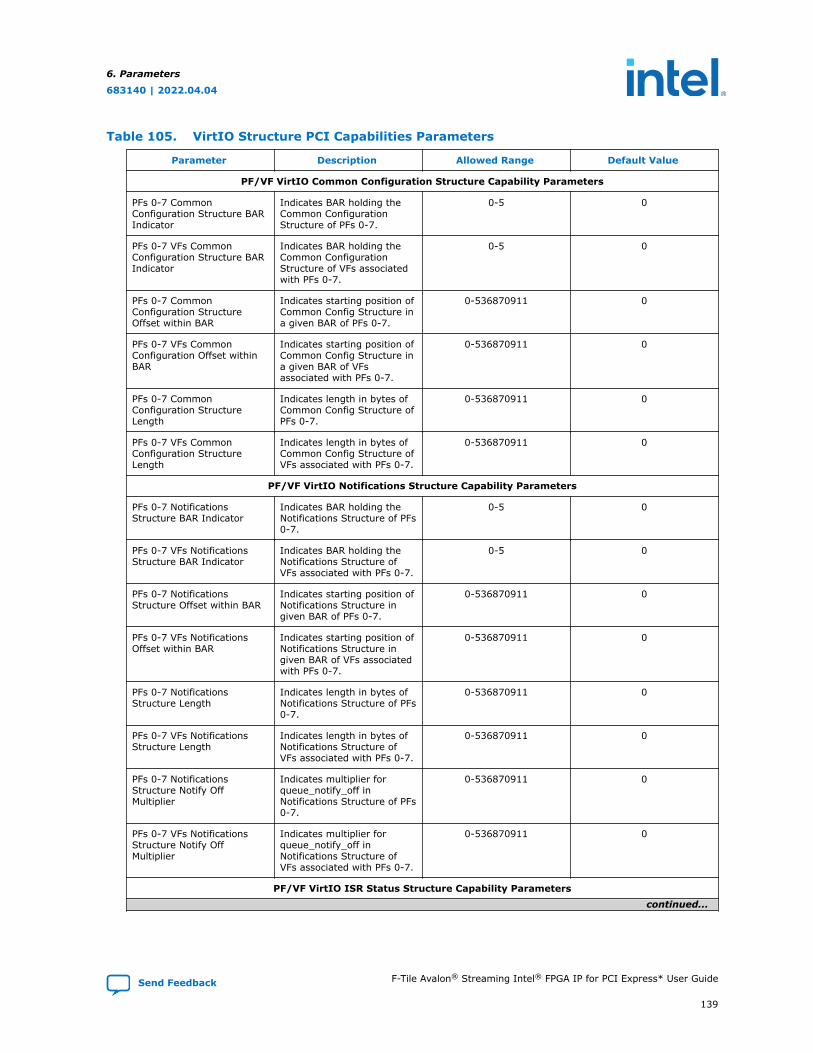
Table 105. VirtIO Structure PCI Capabilities Parameters
Parameter Description Allowed Range Default Value
PF/VF VirtIO Common Configuration Structure Capability Parameters
PFs 0-7 CommonConfiguration Structure BARIndicator
Indicates BAR holding theCommon ConfigurationStructure of PFs 0-7.
0-5 0
PFs 0-7 VFs CommonConfiguration Structure BARIndicator
Indicates BAR holding theCommon ConfigurationStructure of VFs associatedwith PFs 0-7.
0-5 0
PFs 0-7 CommonConfiguration StructureOffset within BAR
Indicates starting position ofCommon Config Structure ina given BAR of PFs 0-7.
0-536870911 0
PFs 0-7 VFs CommonConfiguration Offset withinBAR
Indicates starting position ofCommon Config Structure ina given BAR of VFsassociated with PFs 0-7.
0-536870911 0
PFs 0-7 CommonConfiguration StructureLength
Indicates length in bytes ofCommon Config Structure ofPFs 0-7.
0-536870911 0
PFs 0-7 VFs CommonConfiguration StructureLength
Indicates length in bytes ofCommon Config Structure ofVFs associated with PFs 0-7.
0-536870911 0
PF/VF VirtIO Notifications Structure Capability Parameters
PFs 0-7 NotificationsStructure BAR Indicator
Indicates BAR holding theNotifications Structure of PFs0-7.
0-5 0
PFs 0-7 VFs NotificationsStructure BAR Indicator
Indicates BAR holding theNotifications Structure ofVFs associated with PFs 0-7.
0-5 0
PFs 0-7 NotificationsStructure Offset within BAR
Indicates starting position ofNotifications Structure ingiven BAR of PFs 0-7.
0-536870911 0
PFs 0-7 VFs NotificationsOffset within BAR
Indicates starting position ofNotifications Structure ingiven BAR of VFs associatedwith PFs 0-7.
0-536870911 0
PFs 0-7 NotificationsStructure Length
Indicates length in bytes ofNotifications Structure of PFs0-7.
0-536870911 0
PFs 0-7 VFs NotificationsStructure Length
Indicates length in bytes ofNotifications Structure ofVFs associated with PFs 0-7.
0-536870911 0
PFs 0-7 NotificationsStructure Notify OffMultiplier
Indicates multiplier forqueue_notify_off inNotifications Structure of PFs0-7.
0-536870911 0
PFs 0-7 VFs NotificationsStructure Notify OffMultiplier
Indicates multiplier forqueue_notify_off inNotifications Structure ofVFs associated with PFs 0-7.
0-536870911 0
PF/VF VirtIO ISR Status Structure Capability Parameterscontinued...
6. Parameters
683140 | 2022.04.04
Send Feedback F-Tile Avalon® Streaming Intel® FPGA IP for PCI Express* User Guide
139
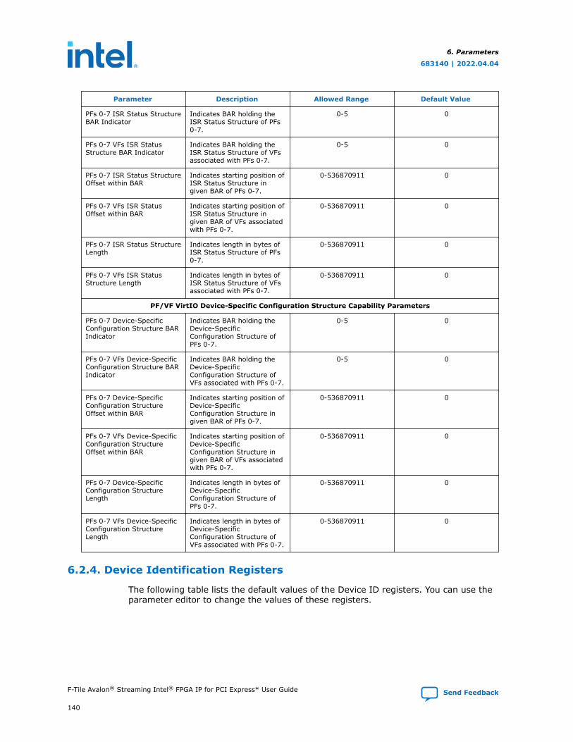
Parameter Description Allowed Range Default Value
PFs 0-7 ISR Status StructureBAR Indicator
Indicates BAR holding theISR Status Structure of PFs0-7.
0-5 0
PFs 0-7 VFs ISR StatusStructure BAR Indicator
Indicates BAR holding theISR Status Structure of VFsassociated with PFs 0-7.
0-5 0
PFs 0-7 ISR Status StructureOffset within BAR
Indicates starting position ofISR Status Structure ingiven BAR of PFs 0-7.
0-536870911 0
PFs 0-7 VFs ISR StatusOffset within BAR
Indicates starting position ofISR Status Structure ingiven BAR of VFs associatedwith PFs 0-7.
0-536870911 0
PFs 0-7 ISR Status StructureLength
Indicates length in bytes ofISR Status Structure of PFs0-7.
0-536870911 0
PFs 0-7 VFs ISR StatusStructure Length
Indicates length in bytes ofISR Status Structure of VFsassociated with PFs 0-7.
0-536870911 0
PF/VF VirtIO Device-Specific Configuration Structure Capability Parameters
PFs 0-7 Device-SpecificConfiguration Structure BARIndicator
Indicates BAR holding theDevice-SpecificConfiguration Structure ofPFs 0-7.
0-5 0
PFs 0-7 VFs Device-SpecificConfiguration Structure BARIndicator
Indicates BAR holding theDevice-SpecificConfiguration Structure ofVFs associated with PFs 0-7.
0-5 0
PFs 0-7 Device-SpecificConfiguration StructureOffset within BAR
Indicates starting position ofDevice-SpecificConfiguration Structure ingiven BAR of PFs 0-7.
0-536870911 0
PFs 0-7 VFs Device-SpecificConfiguration StructureOffset within BAR
Indicates starting position ofDevice-SpecificConfiguration Structure ingiven BAR of VFs associatedwith PFs 0-7.
0-536870911 0
PFs 0-7 Device-SpecificConfiguration StructureLength
Indicates length in bytes ofDevice-SpecificConfiguration Structure ofPFs 0-7.
0-536870911 0
PFs 0-7 VFs Device-SpecificConfiguration StructureLength
Indicates length in bytes ofDevice-SpecificConfiguration Structure ofVFs associated with PFs 0-7.
0-536870911 0
6.2.4. Device Identification Registers
The following table lists the default values of the Device ID registers. You can use theparameter editor to change the values of these registers.
6. Parameters
683140 | 2022.04.04
F-Tile Avalon® Streaming Intel® FPGA IP for PCI Express* User Guide Send Feedback
140
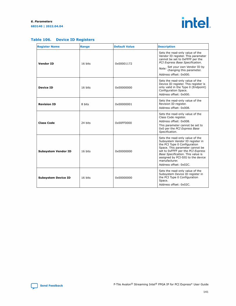
Table 106. Device ID Registers
Register Name Range Default Value Description
Vendor ID 16 bits 0x00001172
Sets the read-only value of theVendor ID register. This parametercannot be set to 0xFFFF per thePCI Express Base Specification.
Note: Set your own Vendor ID bychanging this parameter.
Address offset: 0x000.
Device ID 16 bits 0x00000000
Sets the read-only value of theDevice ID register. This register isonly valid in the Type 0 (Endpoint)Configuration Space.Address offset: 0x000.
Revision ID 8 bits 0x00000001Sets the read-only value of theRevision ID register.Address offset: 0x008.
Class Code 24 bits 0x00FF0000
Sets the read-only value of theClass Code register.Address offset: 0x008.This parameter cannot be set to0x0 per the PCI Express BaseSpecification.
Subsystem Vendor ID 16 bits 0x00000000
Sets the read-only value of theSubsystem Vendor ID register inthe PCI Type 0 ConfigurationSpace. This parameter cannot beset to 0xFFFF per the PCI ExpressBase Specification. This value isassigned by PCI-SIG to the devicemanufacturer.Address offset: 0x02C.
Subsystem Device ID 16 bits 0x00000000
Sets the read-only value of theSubsystem Device ID register inthe PCI Type 0 ConfigurationSpace.Address offset: 0x02C.
6. Parameters
683140 | 2022.04.04
Send Feedback F-Tile Avalon® Streaming Intel® FPGA IP for PCI Express* User Guide
141
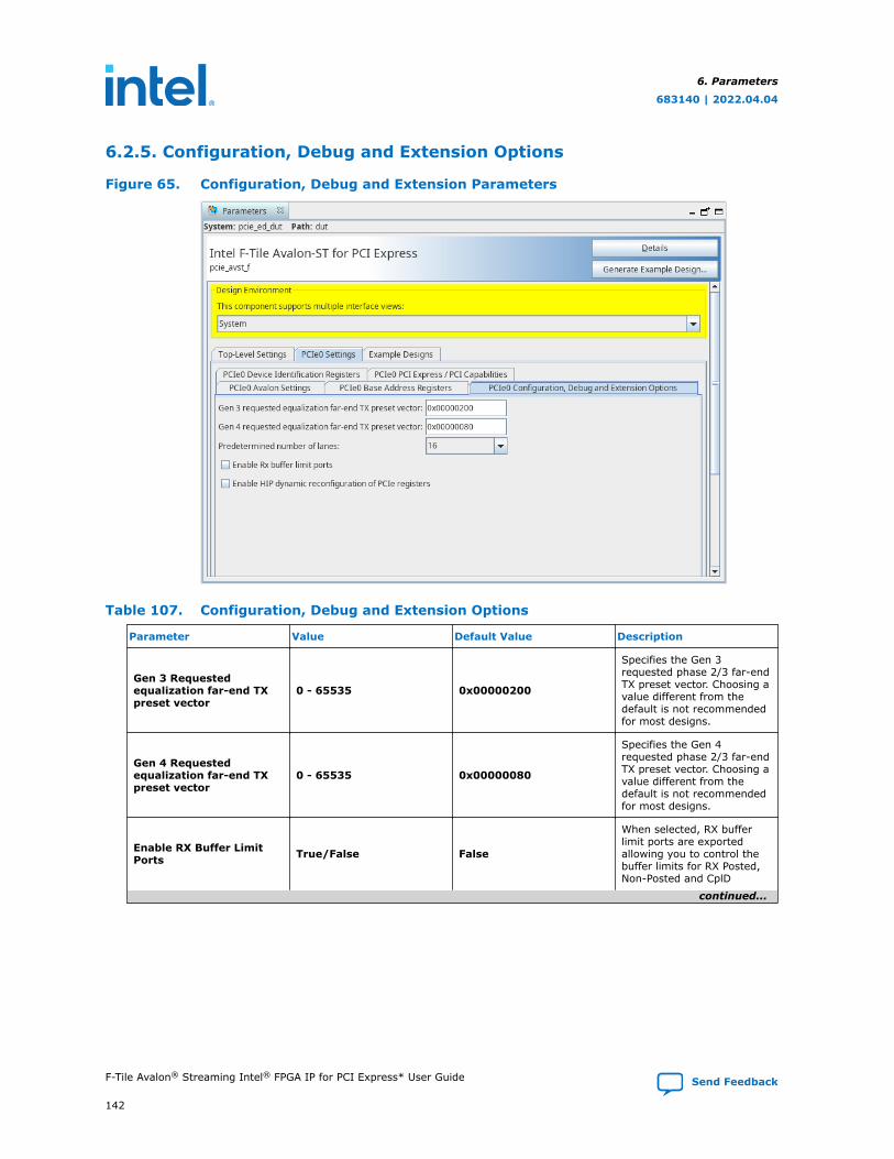
6.2.5. Configuration, Debug and Extension Options
Figure 65. Configuration, Debug and Extension Parameters
Table 107. Configuration, Debug and Extension Options
Parameter Value Default Value Description
Gen 3 Requestedequalization far-end TXpreset vector
0 - 65535 0x00000200
Specifies the Gen 3requested phase 2/3 far-endTX preset vector. Choosing avalue different from thedefault is not recommendedfor most designs.
Gen 4 Requestedequalization far-end TXpreset vector
0 - 65535 0x00000080
Specifies the Gen 4requested phase 2/3 far-endTX preset vector. Choosing avalue different from thedefault is not recommendedfor most designs.
Enable RX Buffer LimitPorts True/False False
When selected, RX bufferlimit ports are exportedallowing you to control thebuffer limits for RX Posted,Non-Posted and CplD
continued...
6. Parameters
683140 | 2022.04.04
F-Tile Avalon® Streaming Intel® FPGA IP for PCI Express* User Guide Send Feedback
142
Parameter Value Default Value Description
packets. Otherwise, theMaximum Buffer Size isused.
Enable HIP dynamicreconfiguration of PCIe*registers
True/False FalseEnable the user Hard IPreconfiguration Avalon-MMinterface.
Predetermined number oflanes
168421
Maximum link width
Defines the number of laneswhich are connected andgood.Used to limit the effectivelink width to ignore 'broken"or "unused" lanes thatdetect a receiver.Indicates the number oflanes to check for exit fromElectrical Idle inPolling.Active and L2.Idle.It is possible that the LTSSMmight detect a receiver on abad or broken lane duringthe Detect Substate.However, it is also possiblethat such a lane might alsofail to exit Electrical Idle andtherefore prevent a valid linkfrom being configured. Thisvalue is referred to as the"Predetermined Number ofLanes" in section 4.2.6.2.1of the PCI Express BaseSpecification.When you have unusedlanes in the system, youmust change the value inthis register to reflect thenumber of lanes. Forinstance, if you find that oneof the used lanes is bad,then you must reduce thevalue of "Predeterminednumber of lanes".
6. Parameters
683140 | 2022.04.04
Send Feedback F-Tile Avalon® Streaming Intel® FPGA IP for PCI Express* User Guide
143
7. TestbenchThis chapter introduces the testbench for an Endpoint design example and a testdriver module. You can create this design example using design flows described inQuick Start Guide chapter of the Intel FPGA F-Tile Avalon streaming IP for PCI ExpressDesign Example User Guide.
The testbench in this design example simulates up to a Gen4 x16 variant.
When configured as an Endpoint variation, the testbench instantiates a designexample with a F-Tile Endpoint and a Root Port BFM containing a second F-Tile(configured as a Root Port) to interface with the Endpoint. The Root Port BFM providesthe following functions:
• A configuration routine that sets up all the basic configuration registers in theEndpoint. This configuration allows the Endpoint application to be the target andinitiator of PCI Express transactions.
• A Verilog HDL procedure interface to initiate PCI Express transactions to theEndpoint.
This testbench simulates the scenario of a single Root Port talking to a singleEndpoint.
The testbench uses a test driver module, altpcietb_bfm_rp_gen4_x16.sv, toinitiate the configuration and memory transactions. At startup, the test driver moduledisplays information from the Root Port and Endpoint Configuration Space registers, sothat you can correlate to the parameters you specified using the Parameter Editor.
Note: The Intel testbench and Root Port BFM provide a simple method to do basic testing ofthe Application Layer logic that interfaces to the variation. This BFM allows you tocreate and run simple task stimuli with configurable parameters to exercise basicfunctionality of the Intel example design. The testbench and Root Port BFM are notintended to be a substitute for a full verification environment. Corner cases andcertain traffic profile stimuli are not covered. Refer to the items listed below for furtherdetails. To ensure the best verification coverage possible, Intel suggests strongly thatyou obtain commercially available PCI Express verification IP and tools, in combinationwith performing extensive hardware testing.
Your Application Layer design may need to handle at least the following scenarios thatare not possible to create with the Intel testbench and the Root Port BFM, or are dueto the limitations of the example design:
683140 | 2022.04.04
Send Feedback
Intel Corporation. All rights reserved. Intel, the Intel logo, and other Intel marks are trademarks of IntelCorporation or its subsidiaries. Intel warrants performance of its FPGA and semiconductor products to currentspecifications in accordance with Intel's standard warranty, but reserves the right to make changes to anyproducts and services at any time without notice. Intel assumes no responsibility or liability arising out of theapplication or use of any information, product, or service described herein except as expressly agreed to inwriting by Intel. Intel customers are advised to obtain the latest version of device specifications before relyingon any published information and before placing orders for products or services.*Other names and brands may be claimed as the property of others.
ISO9001:2015Registered
• It is unable to generate or receive Vendor Defined Messages. Some systemsgenerate Vendor Defined Messages. The Hard IP block simply passes thesemessages on to the Application Layer. Consequently, you should make thedecision, based on your application, whether to design the Application Layer toprocess them.
• It can only handle received read requests that are less than or equal to thecurrently set Maximum payload size option specified under the Device tabunder the PCI Express/PCI Capabilities GUI using the parameter editor. Manysystems are capable of handling larger read requests that are then returned inmultiple completions.
• It always returns a single completion for every read request. Some systems splitcompletions on every 64-byte address boundary.
• It always returns completions in the same order the read requests were issued.Some systems generate the completions out-of-order.
• It is unable to generate zero-length read requests that some systems generate asflush requests following some write transactions. The Application Layer must becapable of generating the completions to the zero-length read requests.
• It uses fixed credit allocation.
• It does not support parity.
• It does not support multi-function designs.
• It incorrectly responds to Type 1 vendor-defined messages with CplD packets.
7.1. Generating Tile Files
The Support-Logic Generation is a pre-synthesis step used to generate tile-relatedfiles needed for simulation and hardware design. The tile files generation is a requiredstep before simulation. You can run Analysis & Elaboration on the Processingmenu in the Intel Quartus Prime Pro Edition software to generate the F-Tile specifictiles file for your design. The Support-Logic Generation command runsautomatically as part of the process.
A successful tile file generation results in the <IP_instance_name>__tiles.x fileswhere x represents necessary file extensions. The generated files are located in yourproject directory and contain the full netlist for simulation and synthesis.
7.2. Endpoint Testbench
The example design and testbench are dynamically generated based on theconfiguration that you choose for the F-Tile IP for PCIe. The testbench uses theparameters that you specify in the Parameter Editor in Intel Quartus Prime.
This testbench simulates up to a x16 PCI Express link using the serial PCI Expressinterface. The testbench design does allow more than one PCI Express link to besimulated at a time. The following figure presents a high level view of the designexample.
7. Testbench
683140 | 2022.04.04
Send Feedback F-Tile Avalon® Streaming Intel® FPGA IP for PCI Express* User Guide
145
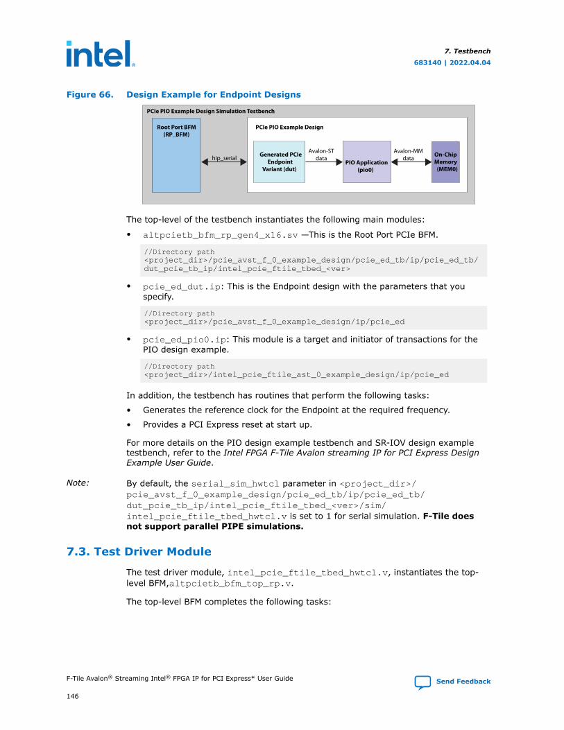
Figure 66. Design Example for Endpoint Designs
Avalon-STdata
Generated PCIeEndpoint
Variant (dut)
On-ChipMemory
(MEM0)
PCIe PIO Example Design
PIO Application(pio0)
hip_serial
Root Port BFM(RP_BFM)
PCIe PIO Example Design Simulation Testbench
Avalon-MMdata
The top-level of the testbench instantiates the following main modules:
• altpcietb_bfm_rp_gen4_x16.sv —This is the Root Port PCIe BFM.
//Directory path<project_dir>/pcie_avst_f_0_example_design/pcie_ed_tb/ip/pcie_ed_tb/dut_pcie_tb_ip/intel_pcie_ftile_tbed_<ver>
• pcie_ed_dut.ip: This is the Endpoint design with the parameters that youspecify.
//Directory path<project_dir>/pcie_avst_f_0_example_design/ip/pcie_ed
• pcie_ed_pio0.ip: This module is a target and initiator of transactions for thePIO design example.
//Directory path<project_dir>/intel_pcie_ftile_ast_0_example_design/ip/pcie_ed
In addition, the testbench has routines that perform the following tasks:
• Generates the reference clock for the Endpoint at the required frequency.
• Provides a PCI Express reset at start up.
For more details on the PIO design example testbench and SR-IOV design exampletestbench, refer to the Intel FPGA F-Tile Avalon streaming IP for PCI Express DesignExample User Guide.
Note: By default, the serial_sim_hwtcl parameter in <project_dir>/pcie_avst_f_0_example_design/pcie_ed_tb/ip/pcie_ed_tb/dut_pcie_tb_ip/intel_pcie_ftile_tbed_<ver>/sim/intel_pcie_ftile_tbed_hwtcl.v is set to 1 for serial simulation. F-Tile doesnot support parallel PIPE simulations.
7.3. Test Driver Module
The test driver module, intel_pcie_ftile_tbed_hwtcl.v, instantiates the top-level BFM,altpcietb_bfm_top_rp.v.
The top-level BFM completes the following tasks:
7. Testbench
683140 | 2022.04.04
F-Tile Avalon® Streaming Intel® FPGA IP for PCI Express* User Guide Send Feedback
146
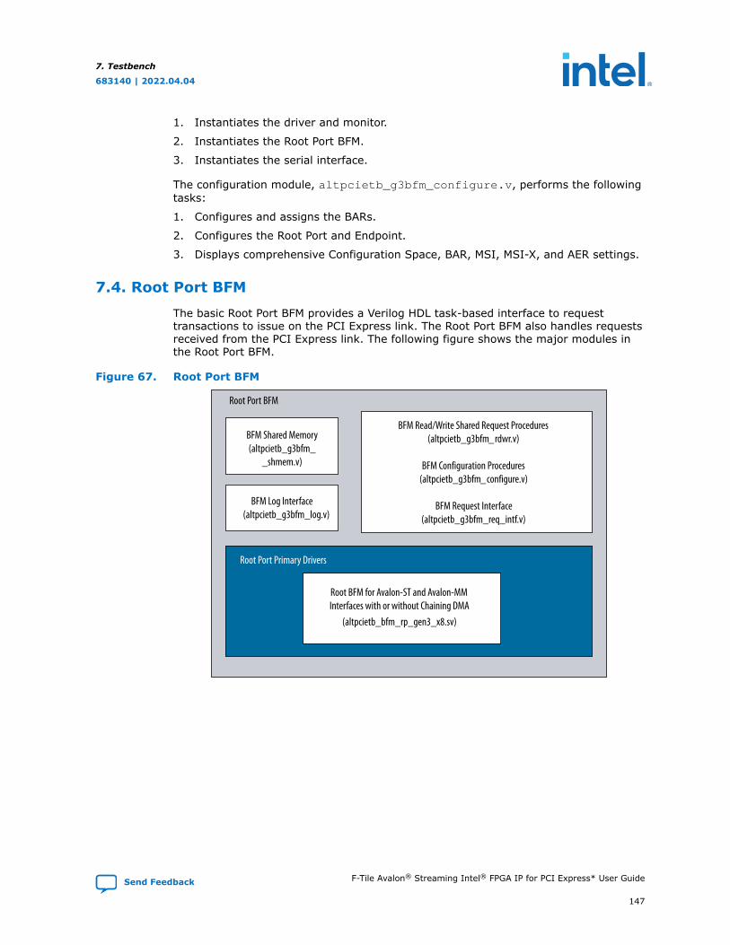
1. Instantiates the driver and monitor.
2. Instantiates the Root Port BFM.
3. Instantiates the serial interface.
The configuration module, altpcietb_g3bfm_configure.v, performs the followingtasks:
1. Configures and assigns the BARs.
2. Configures the Root Port and Endpoint.
3. Displays comprehensive Configuration Space, BAR, MSI, MSI-X, and AER settings.
7.4. Root Port BFM
The basic Root Port BFM provides a Verilog HDL task-based interface to requesttransactions to issue on the PCI Express link. The Root Port BFM also handles requestsreceived from the PCI Express link. The following figure shows the major modules inthe Root Port BFM.
Figure 67. Root Port BFM
BFM Shared Memory(altpcietb_g3bfm_
_shmem.v)
BFM Log Interface(altpcietb_g3bfm_log.v)
Root Port Primary Drivers
Root BFM for Avalon-ST and Avalon-MM Interfaces with or without Chaining DMA
Root Port BFM
BFM Read/Write Shared Request Procedures(altpcietb_g3bfm_rdwr.v)
BFM Configuration Procedures(altpcietb_g3bfm_configure.v)
BFM Request Interface(altpcietb_g3bfm_req_intf.v)
(altpcietb_bfm_rp_gen3_x8.sv)
7. Testbench
683140 | 2022.04.04
Send Feedback F-Tile Avalon® Streaming Intel® FPGA IP for PCI Express* User Guide
147
These modules implement the following functionality:
• BFM Log Interface, altpcietb_g3bfm_log.v andaltpcietb_bfm_rp_gen3_x8.sv: The BFM Log Interface provides routines forwriting commonly formatted messages to the simulator standard output andoptionally to a log file. It also provides controls that stop simulations on errors.
• BFM Read/Write Request Functions, altpcietb_bfm_rp_gen3_x8.sv: Thesefunctions provide the basic BFM calls for PCI Express read and write requests.
• BFM Configuration Functions, altpcietb_g3bfm_configure.v : Thesefunctions provide the BFM calls to request a configuration of the PCI Express linkand the Endpoint Configuration Space registers.
• BFM shared memory, altpcietb_g3bfm_shmem.v: This module provides theRoot Port BFM shared memory. It implements the following functionality:
— Provides data for TX write operations
— Provides data for RX read operations
— Receives data for RX write operations
— Receives data for received completions
• BFM Request Interface, altpcietb_g3bfm_req_intf.v: This interface providesthe low-level interface between the altpcietb_g3bfm_rdwr andaltpcietb_g3bfm_configure procedures or functions and the Root Port RTLModel. This interface stores a write-protected data structure containing the sizesand values programmed in the BAR registers of the Endpoint. It also stores othercritical data used for internal BFM management.
• altpcietb_g3bfm_rdwr.v: This module contains the low-level read and writetasks.
• Avalon-ST Interfaces, altpcietb_g3bfm_vc_intf_ast_common.v: Theseinterface modules handle the Root Port interface model. They take requests fromthe BFM request interface and generate the required PCI Express transactions.They handle completions received from the PCI Express link and notify the BFMrequest interface when requests are complete. Additionally, they handle anyrequests received from the PCI Express link, and store or fetch data from theshared memory before generating the required completions.
In the PIO design example, the apps_type_hwtcl parameter is set to 3. The testsrun under this parameter value are defined in ebfm_cfg_rp_ep_rootport,find_mem_bar and downstream_loop.
The function ebfm_cfg_rp_ep_rootport is described inaltpcietb_g3bfm_configure.v. This function performs the steps necessary toconfigure the root port and the endpoint on the link. It includes:
• Root port memory allocation
• Root port configuration space (base limit, bus number, etc.)
• Endpoint configuration (BAR, Bus Master enable, maxpayload size, etc.)
The functions find_mem_bar and downstream_loop inaltpcietb_bfm_rp_gen3_x8.sv return the BAR implemented and perform thememory Write and Read accesses to the BAR, respectively.
7. Testbench
683140 | 2022.04.04
F-Tile Avalon® Streaming Intel® FPGA IP for PCI Express* User Guide Send Feedback
148
7.4.1. BFM Memory Map
The BFM shared memory is 2 MBs. The BFM shared memory maps to the first 2 MBs ofI/O space and also the first 2 MBs of memory space. When the Endpoint applicationgenerates an I/O or memory transaction in this range, the BFM reads or writes theshared memory.
7.4.2. Configuration Space Bus and Device Numbering
Enumeration assigns the Root Port interface device number 0 on internal bus number0. Use the ebfm_cfg_rp_ep procedure to assign the Endpoint to any device numberon any bus number (greater than 0). The specified bus number is the secondary busin the Root Port Configuration Space.
7.4.3. Configuration of Root Port and Endpoint
Before you issue transactions to the Endpoint, you must configure the Root Port andEndpoint Configuration Space registers.
The ebfm_cfg_rp_ep procedure in altpcietb_g3bfm_configure.v executes thefollowing steps to initialize the Configuration Space:
1. Sets the Root Port Configuration Space to enable the Root Port to sendtransactions on the PCI Express link.
2. Sets the Root Port and Endpoint PCI Express Capability Device Control registers asfollows:
a. Disables Error Reporting in both the Root Port and Endpoint. The BFMdoes not have error handling capability.
b. Enables Relaxed Ordering in both Root Port and Endpoint.
c. Enables Extended Tags for the Endpoint if the Endpoint has that capability.
d. Disables Phantom Functions, Aux Power PM, and No Snoop in both theRoot Port and Endpoint.
e. Sets the Max Payload Size to the value that the Endpoint supports becausethe Root Port supports the maximum payload size.
f. Sets the Root Port Max Read Request Size to 4 KB because the exampleEndpoint design supports breaking the read into as many completions asnecessary.
g. Sets the Endpoint Max Read Request Size equal to the Max PayloadSize because the Root Port does not support breaking the read request intomultiple completions.
3. Assigns values to all the Endpoint BAR registers. The BAR addresses are assignedby the algorithm outlined below.
7. Testbench
683140 | 2022.04.04
Send Feedback F-Tile Avalon® Streaming Intel® FPGA IP for PCI Express* User Guide
149
a. I/O BARs are assigned smallest to largest starting just above the endingaddress of the BFM shared memory in I/O space and continuing as neededthroughout a full 32-bit I/O space.
b. The 32-bit non-prefetchable memory BARs are assigned smallest to largest,starting just above the ending address of the BFM shared memory in memoryspace and continuing as needed throughout a full 32-bit memory space.
c. The value of the addr_map_4GB_limit input to the ebfm_cfg_rp_epprocedure controls the assignment of the 32-bit prefetchable and 64-bitprefetchable memory BARS. The default value of the addr_map_4GB_limitis 0.
If the addr_map_4GB_limit input to the ebfm_cfg_rp_ep procedure is setto 0, then the ebfm_cfg_rp_ep procedure assigns the 32-bit prefetchablememory BARs largest to smallest, starting at the top of 32-bit memory spaceand continuing as needed down to the ending address of the last 32-bit non-prefetchable BAR.
However, if the addr_map_4GB_limit input is set to 1, the address map islimited to 4 GB. The ebfm_cfg_rp_ep procedure assigns 32-bit and 64-bitprefetchable memory BARs largest to smallest, starting at the top of the 32-bitmemory space and continuing as needed down to the ending address of thelast 32-bit non-prefetchable BAR.
d. If the addr_map_4GB_limit input to the ebfm_cfg_rp_ep procedure is setto 0, then the ebfm_cfg_rp_ep procedure assigns the 64-bit prefetchablememory BARs smallest to largest starting at the 4 GB address assigningmemory ascending above the 4 GB limit throughout the full 64-bit memoryspace.
If the addr_map_4 GB_limit input to the ebfm_cfg_rp_ep procedure is setto 1, the ebfm_cfg_rp_ep procedure assigns the 32-bit and the 64-bitprefetchable memory BARs largest to smallest starting at the 4 GB addressand assigning memory by descending below the 4 GB address to memoryaddresses as needed down to the ending address of the last 32-bit non-prefetchable BAR.
The above algorithm cannot always assign values to all BARs when there are afew very large (1 GB or greater) 32-bit BARs. Although assigning addresses toall BARs may be possible, a more complex algorithm would be required toeffectively assign these addresses. However, such a configuration is unlikely tobe useful in real systems. If the procedure is unable to assign the BARs, itdisplays an error message and stops the simulation.
4. Based on the above BAR assignments, the ebfm_cfg_rp_ep procedure assignsthe Root Port Configuration Space address windows to encompass the valid BARaddress ranges.
5. The ebfm_cfg_rp_ep procedure enables master transactions, memory addressdecoding, and I/O address decoding in the Endpoint PCIe control register.
The ebfm_cfg_rp_ep procedure also sets up a bar_table data structure in BFMshared memory that lists the sizes and assigned addresses of all Endpoint BARs. Thisarea of BFM shared memory is write-protected. Consequently, application logic writeaccesses to this area cause a fatal simulation error.
7. Testbench
683140 | 2022.04.04
F-Tile Avalon® Streaming Intel® FPGA IP for PCI Express* User Guide Send Feedback
150
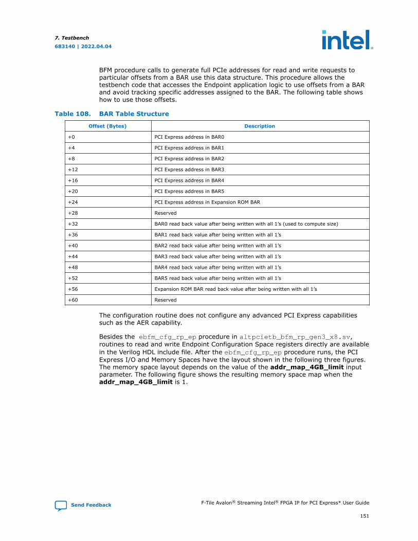
BFM procedure calls to generate full PCIe addresses for read and write requests toparticular offsets from a BAR use this data structure. This procedure allows thetestbench code that accesses the Endpoint application logic to use offsets from a BARand avoid tracking specific addresses assigned to the BAR. The following table showshow to use those offsets.
Table 108. BAR Table Structure
Offset (Bytes) Description
+0 PCI Express address in BAR0
+4 PCI Express address in BAR1
+8 PCI Express address in BAR2
+12 PCI Express address in BAR3
+16 PCI Express address in BAR4
+20 PCI Express address in BAR5
+24 PCI Express address in Expansion ROM BAR
+28 Reserved
+32 BAR0 read back value after being written with all 1’s (used to compute size)
+36 BAR1 read back value after being written with all 1’s
+40 BAR2 read back value after being written with all 1’s
+44 BAR3 read back value after being written with all 1’s
+48 BAR4 read back value after being written with all 1’s
+52 BAR5 read back value after being written with all 1’s
+56 Expansion ROM BAR read back value after being written with all 1’s
+60 Reserved
The configuration routine does not configure any advanced PCI Express capabilitiessuch as the AER capability.
Besides the ebfm_cfg_rp_ep procedure in altpcietb_bfm_rp_gen3_x8.sv,routines to read and write Endpoint Configuration Space registers directly are availablein the Verilog HDL include file. After the ebfm_cfg_rp_ep procedure runs, the PCIExpress I/O and Memory Spaces have the layout shown in the following three figures.The memory space layout depends on the value of the addr_map_4GB_limit inputparameter. The following figure shows the resulting memory space map when theaddr_map_4GB_limit is 1.
7. Testbench
683140 | 2022.04.04
Send Feedback F-Tile Avalon® Streaming Intel® FPGA IP for PCI Express* User Guide
151
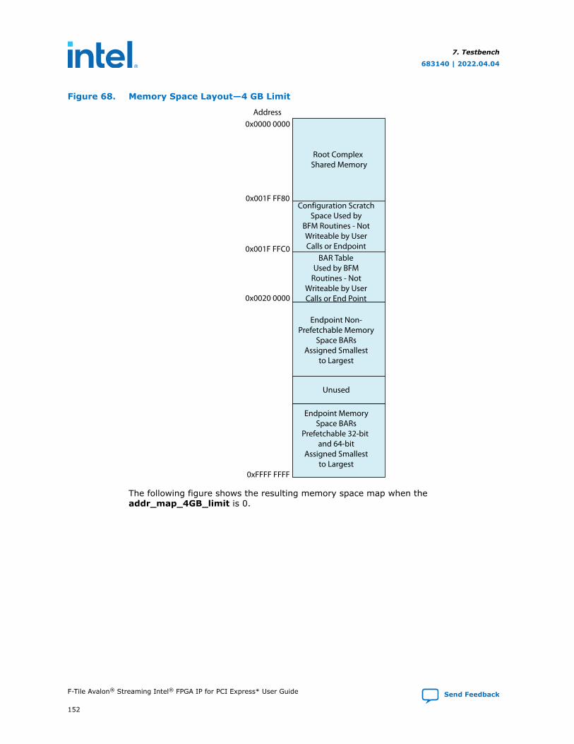
Figure 68. Memory Space Layout—4 GB Limit
Root Complex Shared Memory
Unused
Configuration ScratchSpace Used by
BFM Routines - NotWriteable by UserCalls or Endpoint
BAR TableUsed by BFM
Routines - NotWriteable by UserCalls or End Point
Endpoint Non-Prefetchable Memory
Space BARsAssigned Smallest
to Largest
Endpoint MemorySpace BARs
Prefetchable 32-bit and 64-bit
Assigned Smallestto Largest
0xFFFF FFFF
0x0020 0000
0x0000 0000Address
0x001F FFC0
0x001F FF80
The following figure shows the resulting memory space map when theaddr_map_4GB_limit is 0.
7. Testbench
683140 | 2022.04.04
F-Tile Avalon® Streaming Intel® FPGA IP for PCI Express* User Guide Send Feedback
152
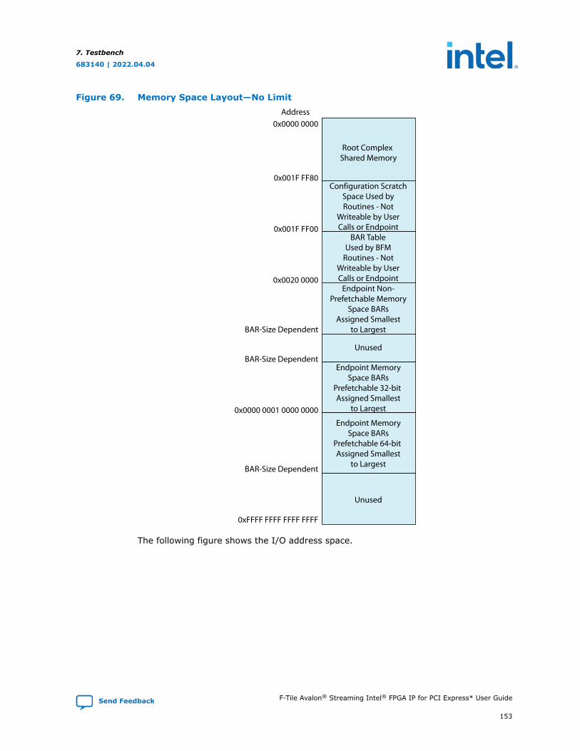
Figure 69. Memory Space Layout—No Limit
Root Complex Shared Memory
Unused
Unused
Configuration ScratchSpace Used byRoutines - Not
Writeable by UserCalls or Endpoint
BAR TableUsed by BFM
Routines - NotWriteable by UserCalls or Endpoint
Endpoint Non-Prefetchable Memory
Space BARsAssigned Smallest
to Largest
Endpoint MemorySpace BARs
Prefetchable 64-bit Assigned Smallest
to Largest
Endpoint MemorySpace BARs
Prefetchable 32-bit Assigned Smallest
to Largest
BAR-Size Dependent
BAR-Size Dependent
BAR-Size Dependent
0x0000 0001 0000 0000
0xFFFF FFFF FFFF FFFF
0x0020 0000
0x0000 0000Address
0x001F FF00
0x001F FF80
The following figure shows the I/O address space.
7. Testbench
683140 | 2022.04.04
Send Feedback F-Tile Avalon® Streaming Intel® FPGA IP for PCI Express* User Guide
153
Figure 70. I/O Address Space
Root Complex Shared Memory
Unused
Configuration ScratchSpace Used by BFM
Routines - NotWriteable by UserCalls or Endpoint
BAR TableUsed by BFM
Routines - NotWriteable by UserCalls or Endpoint
Endpoint I/O Space BARs
Assigned Smallestto Largest
BAR-Size Dependent
0xFFFF FFFF
0x0020 0000
0x0000 0000Address
0x001F FFC0
0x001F FF80
7. Testbench
683140 | 2022.04.04
F-Tile Avalon® Streaming Intel® FPGA IP for PCI Express* User Guide Send Feedback
154
7.4.4. Issuing Read and Write Transactions to the Application Layer
The Root Port Application Layer issues read and write transactions by calling one ofthe ebfm_bar procedures in altpcietb_g3bfm_rdwr.v. The procedures andfunctions listed below are available in the Verilog HDL include filealtpcietb_g3bfm_rdwr.v. The complete list of available procedures and functionsis as follows:
• ebfm_barwr: writes data from BFM shared memory to an offset from a specificEndpoint BAR. This procedure returns as soon as the request has been passed tothe VC interface module for transmission.
• ebfm_barwr_imm: writes a maximum of four bytes of immediate data (passed ina procedure call) to an offset from a specific Endpoint BAR. This procedure returnsas soon as the request has been passed to the VC interface module fortransmission.
• ebfm_barrd_wait: reads data from an offset of a specific Endpoint BAR andstores it in BFM shared memory. This procedure blocks waiting for the completiondata to be returned before returning control to the caller.
• ebfm_barrd_nowt: reads data from an offset of a specific Endpoint BAR andstores it in the BFM shared memory. This procedure returns as soon as the requesthas been passed to the VC interface module for transmission, allowing subsequentreads to be issued in the interim.
These routines take as parameters a BAR number to access the memory space andthe BFM shared memory address of the bar_table data structure that was set up bythe ebfm_cfg_rp_ep procedure. (Refer to Configuration of Root Port and Endpoint.)Using these parameters simplifies the BFM test driver routines that access an offsetfrom a specific BAR and eliminates calculating the addresses assigned to the specifiedBAR.
The Root Port BFM does not support accesses to Endpoint I/O space BARs.
7.5. BFM Procedures and Functions
The BFM includes procedures, functions, and tasks to drive Endpoint applicationtesting. It also includes procedures to run the chaining DMA design example.
The BFM read and write procedures read and write data to BFM shared memory,Endpoint BARs, and specified configuration registers. The procedures and functions areavailable in the Verilog HDL. These procedures and functions support issuing memoryand configuration transactions on the PCI Express link.
7.5.1. ebfm_barwr Procedure
The ebfm_barwr procedure writes a block of data from BFM shared memory to anoffset from the specified Endpoint BAR. The length can be longer than the configuredMAXIMUM_PAYLOAD_SIZE. The procedure breaks the request up into multipletransactions as needed. This routine returns as soon as the last transaction has beenaccepted by the VC interface module.
7. Testbench
683140 | 2022.04.04
Send Feedback F-Tile Avalon® Streaming Intel® FPGA IP for PCI Express* User Guide
155
Location
Syntax ebfm_barwr(bar_table, bar_num, pcie_offset, lcladdr, byte_len, tclass)
Arguments bar_table Address of the Endpoint bar_table structure in BFM shared memory.The bar_table structure stores the address assigned to each BAR sothat the driver code does not need to be aware of the actual assignedaddresses only the application specific offsets from the BAR.
bar_num Number of the BAR used with pcie_offset to determine PCI Expressaddress.
pcie_offset Address offset from the BAR base.
lcladdr BFM shared memory address of the data to be written.
byte_len Length, in bytes, of the data written. Can be 1 to the minimum of thebytes remaining in the BAR space or BFM shared memory.
tclass Traffic class used for the PCI Express transaction.
7.5.2. ebfm_barwr_imm Procedure
The ebfm_barwr_imm procedure writes up to four bytes of data to an offset from thespecified Endpoint BAR.
Location
Syntax ebfm_barwr_imm(bar_table, bar_num, pcie_offset, imm_data, byte_len, tclass)
Arguments bar_table Address of the Endpoint bar_table structure in BFM shared memory.The bar_table structure stores the address assigned to each BAR sothat the driver code does not need to be aware of the actual assignedaddresses only the application specific offsets from the BAR.
bar_num Number of the BAR used with pcie_offset to determine PCI Expressaddress.
pcie_offset Address offset from the BAR base.
imm_data Data to be written. In Verilog HDL, this argument is reg [31:0].Inboth languages, the bits written depend on the length as follows:Length Bits Written• 4: 31 down to 0• 3: 23 down to 0• 2: 15 down to 0• 1: 7 down to 0
byte_len Length of the data to be written in bytes. Maximum length is 4 bytes.
tclass Traffic class to be used for the PCI Express transaction.
7.5.3. ebfm_barrd_wait Procedure
The ebfm_barrd_wait procedure reads a block of data from the offset of thespecified Endpoint BAR and stores it in BFM shared memory. The length can be longerthan the configured maximum read request size; the procedure breaks the request upinto multiple transactions as needed. This procedure waits until all of the completiondata is returned and places it in shared memory.
7. Testbench
683140 | 2022.04.04
F-Tile Avalon® Streaming Intel® FPGA IP for PCI Express* User Guide Send Feedback
156
Location
Syntax ebfm_barrd_wait(bar_table, bar_num, pcie_offset, lcladdr, byte_len, tclass)
Arguments bar_table Address of the Endpoint bar_table structure in BFM shared memory.The bar_table structure stores the address assigned to each BAR so thatthe driver code does not need to be aware of the actual assignedaddresses only the application specific offsets from the BAR.
bar_num Number of the BAR used with pcie_offset to determine PCI Expressaddress.
pcie_offset Address offset from the BAR base.
lcladdr BFM shared memory address where the read data is stored.
byte_len Length, in bytes, of the data to be read. Can be 1 to the minimum ofthe bytes remaining in the BAR space or BFM shared memory.
tclass Traffic class used for the PCI Express transaction.
7.5.4. ebfm_barrd_nowt Procedure
The ebfm_barrd_nowt procedure reads a block of data from the offset of thespecified Endpoint BAR and stores the data in BFM shared memory. The length can belonger than the configured maximum read request size; the procedure breaks therequest up into multiple transactions as needed. This routine returns as soon as thelast read transaction has been accepted by the VC interface module, allowingsubsequent reads to be issued immediately.
Location
Syntax ebfm_barrd_nowt(bar_table, bar_num, pcie_offset, lcladdr, byte_len, tclass)
Arguments bar_table Address of the Endpoint bar_table structure in BFM shared memory.
bar_num Number of the BAR used with pcie_offset to determine PCI Expressaddress.
pcie_offset Address offset from the BAR base.
lcladdr BFM shared memory address where the read data is stored.
byte_len Length, in bytes, of the data to be read. Can be 1 to the minimum ofthe bytes remaining in the BAR space or BFM shared memory.
tclass Traffic Class to be used for the PCI Express transaction.
7.5.5. ebfm_cfgwr_imm_wait Procedure
The ebfm_cfgwr_imm_wait procedure writes up to four bytes of data to thespecified configuration register. This procedure waits until the write completion hasbeen returned.
Location
Syntax ebfm_cfgwr_imm_wait(bus_num, dev_num, fnc_num, imm_regb_ad, regb_ln, imm_data,compl_status
Arguments bus_num PCI Express bus number of the target device.
dev_num PCI Express device number of the target device.
fnc_num Function number in the target device to be accessed.
continued...
7. Testbench
683140 | 2022.04.04
Send Feedback F-Tile Avalon® Streaming Intel® FPGA IP for PCI Express* User Guide
157
Location
regb_ad Byte-specific address of the register to be written.
regb_ln Length, in bytes, of the data written. Maximum length is four bytes. Theregb_ln and the regb_ad arguments cannot cross a DWORDboundary.
imm_data Data to be written.This argument is reg [31:0].The bits written depend on the length:• 4: 31 down to 0• 3: 23 down to 0• 2: 15 down to 0• 1: 7 down to 0
compl_status This argument is reg [2:0].This argument is the completion status as specified in the PCI Expressspecification. The following encodings are defined:• 3’b000: SC— Successful completion• 3’b001: UR— Unsupported Request• 3’b010: CRS — Configuration Request Retry Status• 3’b100: CA — Completer Abort
7.5.6. ebfm_cfgwr_imm_nowt Procedure
The ebfm_cfgwr_imm_nowt procedure writes up to four bytes of data to thespecified configuration register. This procedure returns as soon as the VC interfacemodule accepts the transaction, allowing other writes to be issued in the interim. Usethis procedure only when successful completion status is expected.
Location
Syntax ebfm_cfgwr_imm_nowt(bus_num, dev_num, fnc_num, imm_regb_adr, regb_len,imm_data)
Arguments bus_num PCI Express bus number of the target device.
dev_num PCI Express device number of the target device.
fnc_num Function number in the target device to be accessed.
regb_ad Byte-specific address of the register to be written.
regb_ln Length, in bytes, of the data written. Maximum length is four bytes, Theregb_ln the regb_ad arguments cannot cross a DWORD boundary.
imm_data Data to be writtenThis argument is reg [31:0].In both languages, the bits written depend on the length. The followingencodes are defined.• 4: [31:0]• 3: [23:0]• 2: [15:0]• 1: [7:0]
7.5.7. ebfm_cfgrd_wait Procedure
The ebfm_cfgrd_wait procedure reads up to four bytes of data from the specifiedconfiguration register and stores the data in BFM shared memory. This procedurewaits until the read completion has been returned.
7. Testbench
683140 | 2022.04.04
F-Tile Avalon® Streaming Intel® FPGA IP for PCI Express* User Guide Send Feedback
158
Location
Syntax ebfm_cfgrd_wait(bus_num, dev_num, fnc_num, regb_ad, regb_ln, lcladdr,compl_status)
Arguments bus_num PCI Express bus number of the target device.
dev_num PCI Express device number of the target device.
fnc_num Function number in the target device to be accessed.
regb_ad Byte-specific address of the register to be written.
regb_ln Length, in bytes, of the data read. Maximum length is four bytes. Theregb_ln and the regb_ad arguments cannot cross a DWORDboundary.
lcladdr BFM shared memory address of where the read data should be placed.
compl_status Completion status for the configuration transaction.This argument is reg [2:0].In both languages, this is the completion status as specified in the PCIExpress specification. The following encodings are defined.• 3’b000: SC— Successful completion• 3’b001: UR— Unsupported Request• 3’b010: CRS — Configuration Request Retry Status• 3’b100: CA — Completer Abort
7.5.8. ebfm_cfgrd_nowt Procedure
The ebfm_cfgrd_nowt procedure reads up to four bytes of data from the specifiedconfiguration register and stores the data in the BFM shared memory. This procedurereturns as soon as the VC interface module has accepted the transaction, allowingother reads to be issued in the interim. Use this procedure only when successfulcompletion status is expected and a subsequent read or write with a wait can be usedto guarantee the completion of this operation.
Location
Syntax ebfm_cfgrd_nowt(bus_num, dev_num, fnc_num, regb_ad, regb_ln, lcladdr)
Arguments bus_num PCI Express bus number of the target device.
dev_num PCI Express device number of the target device.
fnc_num Function number in the target device to be accessed.
regb_ad Byte-specific address of the register to be written.
regb_ln Length, in bytes, of the data written. Maximum length is four bytes. Theregb_ln and regb_ad arguments cannot cross a DWORD boundary.
lcladdr BFM shared memory address where the read data should be placed.
7.5.9. BFM Configuration Procedures
All Verilog HDL arguments are type integer and are input-only unless specifiedotherwise.
7. Testbench
683140 | 2022.04.04
Send Feedback F-Tile Avalon® Streaming Intel® FPGA IP for PCI Express* User Guide
159
7.5.9.1. ebfm_cfg_rp_ep Procedure
The ebfm_cfg_rp_ep procedure configures the Root Port and Endpoint ConfigurationSpace registers for operation.
Location
Syntax ebfm_cfg_rp_ep(bar_table, ep_bus_num, ep_dev_num, rp_max_rd_req_size,display_ep_config, addr_map_4GB_limit)
Arguments bar_table Address of the Endpoint bar_table structure in BFM shared memory.This routine populates the bar_table structure. The bar_tablestructure stores the size of each BAR and the address values assigned toeach BAR. The address of the bar_table structure is passed to allsubsequent read and write procedure calls that access an offset from aparticular BAR.
ep_bus_num PCI Express bus number of the target device. This number can be anyvalue greater than 0. The Root Port uses this as the secondary busnumber.
ep_dev_num PCI Express device number of the target device. This number can beany value. The Endpoint is automatically assigned this value when itreceives the first configuration transaction.
rp_max_rd_req_size Maximum read request size in bytes for reads issued by the Root Port.This parameter must be set to the maximum value supported by theEndpoint Application Layer. If the Application Layer only supports readsof the MAXIMUM_PAYLOAD_SIZE, then this can be set to 0 and the readrequest size is set to the maximum payload size. Valid values for thisargument are 0, 128, 256, 512, 1,024, 2,048 and 4,096.
display_ep_config When set to 1 many of the Endpoint Configuration Space registers aredisplayed after they have been initialized, causing some additional readsof registers that are not normally accessed during the configurationprocess such as the Device ID and Vendor ID.
addr_map_4GB_limit When set to 1 the address map of the simulation system is limited to 4GB. Any 64-bit BARs are assigned below the 4 GB limit.
7.5.9.2. ebfm_cfg_decode_bar Procedure
The ebfm_cfg_decode_bar procedure analyzes the information in the BAR table forthe specified BAR and returns details about the BAR attributes.
Location
Syntax ebfm_cfg_decode_bar(bar_table, bar_num, log2_size, is_mem, is_pref, is_64b)
Arguments bar_table Address of the Endpoint bar_table structure in BFM shared memory.
bar_num BAR number to analyze.
log2_size This argument is set by the procedure to the log base 2 of the size ofthe BAR. If the BAR is not enabled, this argument is set to 0.
is_mem The procedure sets this argument to indicate if the BAR is a memoryspace BAR (1) or I/O Space BAR (0).
is_pref The procedure sets this argument to indicate if the BAR is a prefetchableBAR (1) or non-prefetchable BAR (0).
is_64b The procedure sets this argument to indicate if the BAR is a 64-bit BAR(1) or 32-bit BAR (0). This is set to 1 only for the lower numbered BARof the pair.
7. Testbench
683140 | 2022.04.04
F-Tile Avalon® Streaming Intel® FPGA IP for PCI Express* User Guide Send Feedback
160
7.5.10. BFM Shared Memory Access Procedures
These procedures and functions support accessing the BFM shared memory.
7.5.10.1. Shared Memory Constants
Table 109. Constants: Verilog HDL Type INTEGER
Constant Description
SHMEM_FILL_ZEROS Specifies a data pattern of all zeros
SHMEM_FILL_BYTE_INC Specifies a data pattern of incrementing 8-bit bytes (0x00, 0x01, 0x02,etc.)
SHMEM_FILL_WORD_INC Specifies a data pattern of incrementing 16-bit words (0x0000, 0x0001,0x0002, etc.)
SHMEM_FILL_DWORD_INC Specifies a data pattern of incrementing 32-bit DWORDs (0x00000000,0x00000001, 0x00000002, etc.)
SHMEM_FILL_QWORD_INC Specifies a data pattern of incrementing 64-bit qwords(0x0000000000000000, 0x0000000000000001, 0x0000000000000002,etc.)
SHMEM_FILL_ONE Specifies a data pattern of all ones
7.5.10.2. shmem_write Task
The shmem_write procedure writes data to the BFM shared memory.
Location
Syntax shmem_write(addr, data, leng)
Arguments addr BFM shared memory starting address for writing data
data Data to write to BFM shared memory.This parameter is implemented as a 64-bit vector. leng is 1–8 bytes.Bits 7 down to 0 are written to the location specified by addr; bits 15down to 8 are written to the addr+1 location, etc.
length Length, in bytes, of data written
7.5.10.3. shmem_read Function
The shmem_read function reads data to the BFM shared memory.
Location
Syntax data:= shmem_read(addr, leng)
Arguments addr BFM shared memory starting address for reading data
leng Length, in bytes, of data read
Return data Data read from BFM shared memory.This parameter is implemented as a 64-bit vector. leng is 1- 8 bytes. Ifleng is less than 8 bytes, only the corresponding least significant bits ofthe returned data are valid.Bits 7 down to 0 are read from the location specified by addr; bits 15down to 8 are read from the addr+1 location, etc.
7. Testbench
683140 | 2022.04.04
Send Feedback F-Tile Avalon® Streaming Intel® FPGA IP for PCI Express* User Guide
161
7.5.10.4. shmem_display Verilog HDL Function
The shmem_display Verilog HDL function displays a block of data from the BFMshared memory.
Location
Syntax Verilog HDL: dummy_return:=shmem_display(addr, leng, word_size, flag_addr,msg_type);
Arguments addr BFM shared memory starting address for displaying data.
leng Length, in bytes, of data to display.
word_size Size of the words to display. Groups individual bytes into words. Validvalues are 1, 2, 4, and 8.
flag_addr Adds a <== flag to the end of the display line containing this address.Useful for marking specific data. Set to a value greater than 2**21 (sizeof BFM shared memory) to suppress the flag.
msg_type Specifies the message type to be displayed at the beginning of eachline. See “BFM Log and Message Procedures” on page 18–37 for moreinformation about message types. Set to one of the constants definedin.
7.5.10.5. shmem_fill Procedure
The shmem_fill procedure fills a block of BFM shared memory with a specified datapattern.
Location
Syntax shmem_fill(addr, mode, leng, init)
Arguments addr BFM shared memory starting address for filling data.
mode Data pattern used for filling the data. Should be one of the constantsdefined in section Shared Memory Constants.
leng Length, in bytes, of data to fill. If the length is not a multiple of theincrementing data pattern width, then the last data pattern is truncatedto fit.
init Initial data value used for incrementing data pattern modes. Thisargument is reg [63:0].The necessary least significant bits are used for the data patterns thatare smaller than 64 bits.
7.5.10.6. shmem_chk_ok Function
The shmem_chk_ok function checks a block of BFM shared memory against aspecified data pattern.
Location
Syntax result:= shmem_chk_ok(addr, mode, leng, init, display_error)
Arguments addr BFM shared memory starting address for checking data.
mode Data pattern used for checking the data. Should be one of the constantsdefined in section “Shared Memory Constants”.
leng Length, in bytes, of data to check.
continued...
7. Testbench
683140 | 2022.04.04
F-Tile Avalon® Streaming Intel® FPGA IP for PCI Express* User Guide Send Feedback
162
Location
init This argument is reg [63:0].The necessary least significant bits areused for the data patterns that are smaller than 64-bits.
display_error When set to 1, this argument displays the data failing comparison onthe simulator standard output.
Return Result Result is 1-bit.• 1’b1 — Data patterns compared successfully• 1’b0 — Data patterns did not compare successfully
7.5.11. BFM Log and Message Procedures
These procedures provide support for displaying messages in a common format,suppressing informational messages, and stopping simulation on specific messagetypes.
The following constants define the type of message and their values determinewhether a message is displayed or simulation is stopped after a specific message.Each displayed message has a specific prefix, based on the message type in thefollowing table.
You can suppress the display of certain message types. The default values determiningwhether a message type is displayed are defined in the following table. To change thedefault message display, modify the display default value with a procedure call toebfm_log_set_suppressed_msg_mask.
Certain message types also stop simulation after the message is displayed. Thefollowing table shows the default value determining whether a message type stopssimulation. You can specify whether simulation stops for particular messages with theprocedure ebfm_log_set_stop_on_msg_mask.
All of these log message constants type integer.
Table 110. Log Messages
Constant(Message
Type)
Description Mask BitNo
Displayby Default
SimulationStops byDefault
MessagePrefix
EBFM_MSG_DEBUG
Specifies debug messages. 0 No No DEBUG:
EBFM_MSG_INFO
Specifies informational messages,such as configuration registervalues, starting and ending of tests.
1 Yes No INFO:
EBFM_MSG_WARNING
Specifies warning messages, suchas tests being skipped due to thespecific configuration.
2 Yes No WARNING:
EBFM_MSG_ERROR_INFO
Specifies additional information foran error. Use this message todisplay preliminary informationbefore an error message that stopssimulation.
3 Yes No ERROR:
continued...
7. Testbench
683140 | 2022.04.04
Send Feedback F-Tile Avalon® Streaming Intel® FPGA IP for PCI Express* User Guide
163
Constant(Message
Type)
Description Mask BitNo
Displayby Default
SimulationStops byDefault
MessagePrefix
EBFM_MSG_ERROR_CONTINUE
Specifies a recoverable error thatallows simulation to continue. Usethis error for data comparisonfailures.
4 Yes No ERROR:
EBFM_MSG_ERROR_FATAL
Specifies an error that stopssimulation because the error leavesthe testbench in a state wherefurther simulation is not possible.
N/A YesCannotsuppress
YesCannot suppress
FATAL:
EBFM_MSG_ERROR_FATAL_TB_ERR
Used for BFM test driver or RootPort BFM fatal errors. Specifies anerror that stops simulation becausethe error leaves the testbench in astate where further simulation isnot possible. Use this errormessage for errors that occur dueto a problem in the BFM test drivermodule or the Root Port BFM, thatare not caused by the EndpointApplication Layer being tested.
N/A YCannotsuppress
YCannot suppress
FATAL:
7.5.11.1. ebfm_display Verilog HDL Function
The ebfm_display procedure or function displays a message of the specified type tothe simulation standard output and also the log file if ebfm_log_open is called.
A message can be suppressed, simulation can be stopped or both based on the defaultsettings of the message type and the value of the bit mask when each of theprocedures listed below is called. You can call one or both of these procedures basedon what messages you want displayed and whether or not you want simulation to stopfor specific messages.
• When ebfm_log_set_suppressed_msg_mask is called, the display of themessage might be suppressed based on the value of the bit mask.
• When ebfm_log_set_stop_on_msg_mask is called, the simulation can bestopped after the message is displayed, based on the value of the bit mask.
Location
Syntax Verilog HDL: dummy_return:=ebfm_display(msg_type, message);
Argument msg_type Message type for the message. Should be one of the constants definedin Shared Memory Constants on page 161.
message The message string is limited to a maximum of 100 characters. Also,because Verilog HDL does not allow variable length strings, this routinestrips off leading characters of 8’h00 before displaying the message.
Return always 0 Applies only to the Verilog HDL routine.
7.5.11.2. ebfm_log_stop_sim Verilog HDL Function
The ebfm_log_stop_sim procedure stops the simulation.
7. Testbench
683140 | 2022.04.04
F-Tile Avalon® Streaming Intel® FPGA IP for PCI Express* User Guide Send Feedback
164
Location
Syntax Verilog HDL: return:=ebfm_log_stop_sim(success);
Argument success When set to a 1, this process stops the simulation with a messageindicating successful completion. The message is prefixed withSUCCESS.Otherwise, this process stops the simulation with a message indicatingunsuccessful completion. The message is prefixed with FAILURE.
Return Always 0 This value applies only to the Verilog HDL function.
7.5.11.3. ebfm_log_set_suppressed_msg_mask Task
The ebfm_log_set_suppressed_msg_mask procedure controls which messagetypes are suppressed.
Location
Syntax ebfm_log_set_suppressed_msg_mask (msg_mask)
Argument msg_mask This argument is reg [EBFM_MSG_ERROR_CONTINUE:EBFM_MSG_DEBUG].
A 1 in a specific bit position of the msg_mask causes messages of thetype corresponding to the bit position to be suppressed.
7.5.11.4. ebfm_log_set_stop_on_msg_mask Verilog HDL Task
The ebfm_log_set_stop_on_msg_mask procedure controls which message typesstop simulation. This procedure alters the default behavior of the simulation whenerrors occur as described in the BFM Log and Message Procedures.
Location
Syntax ebfm_log_set_stop_on_msg_mask (msg_mask)
Argument msg_mask This argument is reg[EBFM_MSG_ERROR_CONTINUE:EBFM_MSG_DEBUG].A 1 in a specific bit position of the msg_mask causes messages of thetype corresponding to the bit position to stop the simulation after themessage is displayed.
7.5.11.5. ebfm_log_open Verilog HDL Function
The ebfm_log_open procedure opens a log file of the specified name. All displayedmessages are called by ebfm_display and are written to this log file as simulatorstandard output.
Location
Syntax ebfm_log_open (fn)
Argument fn This argument is type string and provides the file name of log file tobe opened.
7.5.11.6. ebfm_log_close Verilog HDL Function
The ebfm_log_close procedure closes the log file opened by a previous call toebfm_log_open.
7. Testbench
683140 | 2022.04.04
Send Feedback F-Tile Avalon® Streaming Intel® FPGA IP for PCI Express* User Guide
165
Location
Syntax ebfm_log_close
Argument NONE
7.5.12. Verilog HDL Formatting Functions
7.5.12.1. himage1
This function creates a one-digit hexadecimal string representation of the inputargument that can be concatenated into a larger message string and passed toebfm_display.
Location
Syntax string:= himage(vec)
Argument vec Input data type reg with a range of 3:0.
Return range string Returns a 1-digit hexadecimal representation of the input argument.Return data is type reg with a range of 8:1
7.5.12.2. himage2
This function creates a two-digit hexadecimal string representation of the inputargument that can be concatenated into a larger message string and passed toebfm_display.
Location
Syntax string:= himage(vec)
Argument range vec Input data type reg with a range of 7:0.
Return range string Returns a 2-digit hexadecimal presentation of the input argument,padded with leading 0s, if they are needed. Return data is type reg witha range of 16:1
7.5.12.3. himage4
This function creates a four-digit hexadecimal string representation of the inputargument can be concatenated into a larger message string and passed toebfm_display.
Location
Syntax string:= himage(vec)
Argument range vec Input data type reg with a range of 15:0.
Return range Returns a four-digit hexadecimal representation of the input argument, padded with leading 0s, if theyare needed. Return data is type reg with a range of 32:1.
7.5.12.4. himage8
This function creates an 8-digit hexadecimal string representation of the inputargument that can be concatenated into a larger message string and passed toebfm_display.
7. Testbench
683140 | 2022.04.04
F-Tile Avalon® Streaming Intel® FPGA IP for PCI Express* User Guide Send Feedback
166
Location
Syntax string:= himage(vec)
Argument range vec Input data type reg with a range of 31:0.
Return range string Returns an 8-digit hexadecimal representation of the input argument,padded with leading 0s, if they are needed. Return data is type reg witha range of 64:1.
7.5.12.5. himage16
This function creates a 16-digit hexadecimal string representation of the inputargument that can be concatenated into a larger message string and passed toebfm_display.
Location
Syntax string:= himage(vec)
Argument range vec Input data type reg with a range of 63:0.
Return range string Returns a 16-digit hexadecimal representation of the input argument,padded with leading 0s, if they are needed. Return data is type reg witha range of 128:1.
7.5.12.6. dimage1
This function creates a one-digit decimal string representation of the input argumentthat can be concatenated into a larger message string and passed to ebfm_display.
Location altpcietb_bfm_driver_rp.valtpcietb_bfm_log.v
Syntax string:= dimage(vec)
Argument range vec Input data type reg with a range of 31:0.
Return range string Returns a 1-digit decimal representation of the input argument that ispadded with leading 0s if necessary. Return data is type reg with arange of 8:1.Returns the letter U if the value cannot be represented.
7.5.12.7. dimage2
This function creates a two-digit decimal string representation of the input argumentthat can be concatenated into a larger message string and passed to ebfm_display.
Location
Syntax string:= dimage(vec)
Argument range vec Input data type reg with a range of 31:0.
Return range string Returns a 2-digit decimal representation of the input argument that ispadded with leading 0s if necessary. Return data is type reg with arange of 16:1.Returns the letter U if the value cannot be represented.
7. Testbench
683140 | 2022.04.04
Send Feedback F-Tile Avalon® Streaming Intel® FPGA IP for PCI Express* User Guide
167
7.5.12.8. dimage3
This function creates a three-digit decimal string representation of the input argumentthat can be concatenated into a larger message string and passed to ebfm_display.
Location
Syntax string:= dimage(vec)
Argument range vec Input data type reg with a range of 31:0.
Return range string Returns a 3-digit decimal representation of the input argument that ispadded with leading 0s if necessary. Return data is type reg with arange of 24:1.Returns the letter U if the value cannot be represented.
7.5.12.9. dimage4
This function creates a four-digit decimal string representation of the input argumentthat can be concatenated into a larger message string and passed to ebfm_display.
Location
Syntax string:= dimage(vec)
Argument range vec Input data type reg with a range of 31:0.
Return range string Returns a 4-digit decimal representation of the input argument that ispadded with leading 0s if necessary. Return data is type reg with arange of 32:1.Returns the letter U if the value cannot be represented.
7.5.12.10. dimage5
This function creates a five-digit decimal string representation of the input argumentthat can be concatenated into a larger message string and passed to ebfm_display.
Location
Syntax string:= dimage(vec)
Argument range vec Input data type reg with a range of 31:0.
Return range string Returns a 5-digit decimal representation of the input argument that ispadded with leading 0s if necessary. Return data is type reg with arange of 40:1.Returns the letter U if the value cannot be represented.
7.5.12.11. dimage6
This function creates a six-digit decimal string representation of the input argumentthat can be concatenated into a larger message string and passed to ebfm_display.
Location
Syntax string:= dimage(vec)
Argument range vec Input data type reg with a range of 31:0.
Return range string Returns a 6-digit decimal representation of the input argument that ispadded with leading 0s if necessary. Return data is type reg with arange of 48:1.Returns the letter U if the value cannot be represented.
7. Testbench
683140 | 2022.04.04
F-Tile Avalon® Streaming Intel® FPGA IP for PCI Express* User Guide Send Feedback
168
7.5.12.12. dimage7
This function creates a seven-digit decimal string representation of the input argumentthat can be concatenated into a larger message string and passed to ebfm_display.
Location
Syntax string:= dimage(vec)
Argument range vec Input data type reg with a range of 31:0.
Return range string Returns a 7-digit decimal representation of the input argument that ispadded with leading 0s if necessary. Return data is type reg with arange of 56:1.Returns the letter <U> if the value cannot be represented.
7. Testbench
683140 | 2022.04.04
Send Feedback F-Tile Avalon® Streaming Intel® FPGA IP for PCI Express* User Guide
169
8. Troubleshooting/DebuggingAs you bring up your PCI Express system, you may face issues related to FPGAconfiguration, link training, BIOS enumeration, data transfer, and so on. This chaptersuggests some strategies to resolve the common issues that occur during bring-up.
8.1. Hardware
Typically, PCI Express link-up involves the following steps:
1. Link training
2. BIOS enumeration and data transfer
The following sections describe the flow to debug link issues during the hardwarebring-up. Intel recommends a systematic approach to diagnosing issues as illustratedin the following figure.
Additionally, you can use the F-Tile Debug Toolkit for debugging the PCIe links whenusing the F-Tile Avalon-ST IP for PCI Express. The F-Tile Debug Toolkit includes thefollowing features:
• Protocol and link status information
• Basic and advanced debugging capabilities including register read access
683140 | 2022.04.04
Send Feedback
Intel Corporation. All rights reserved. Intel, the Intel logo, and other Intel marks are trademarks of IntelCorporation or its subsidiaries. Intel warrants performance of its FPGA and semiconductor products to currentspecifications in accordance with Intel's standard warranty, but reserves the right to make changes to anyproducts and services at any time without notice. Intel assumes no responsibility or liability arising out of theapplication or use of any information, product, or service described herein except as expressly agreed to inwriting by Intel. Intel customers are advised to obtain the latest version of device specifications before relyingon any published information and before placing orders for products or services.*Other names and brands may be claimed as the property of others.
ISO9001:2015Registered
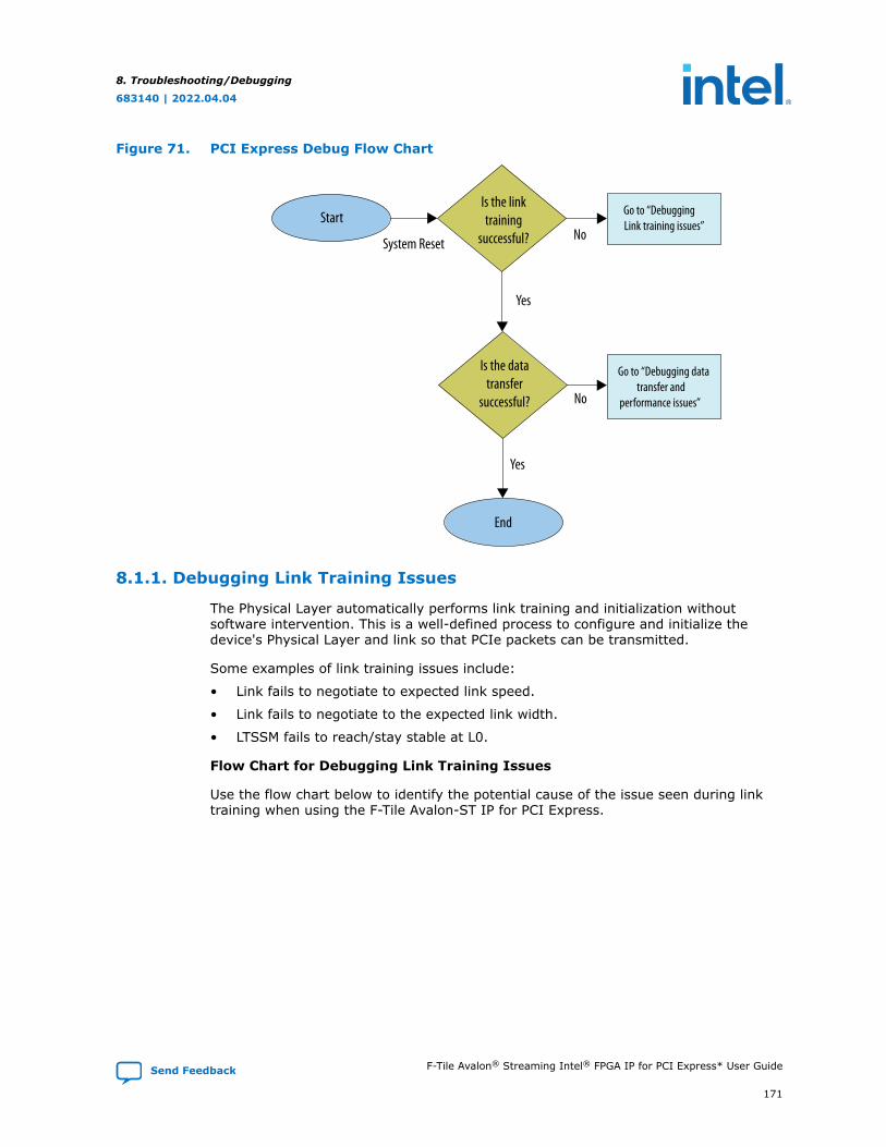
Figure 71. PCI Express Debug Flow Chart
No
No
Yes
Yes
Go to “Debugging data transfer and
performance issues”
Go to “Debugging Link training issues”
System Reset
Start
End
Is the data transfer
successful?
Is the link training
successful?
8.1.1. Debugging Link Training Issues
The Physical Layer automatically performs link training and initialization withoutsoftware intervention. This is a well-defined process to configure and initialize thedevice's Physical Layer and link so that PCIe packets can be transmitted.
Some examples of link training issues include:
• Link fails to negotiate to expected link speed.
• Link fails to negotiate to the expected link width.
• LTSSM fails to reach/stay stable at L0.
Flow Chart for Debugging Link Training Issues
Use the flow chart below to identify the potential cause of the issue seen during linktraining when using the F-Tile Avalon-ST IP for PCI Express.
8. Troubleshooting/Debugging
683140 | 2022.04.04
Send Feedback F-Tile Avalon® Streaming Intel® FPGA IP for PCI Express* User Guide
171
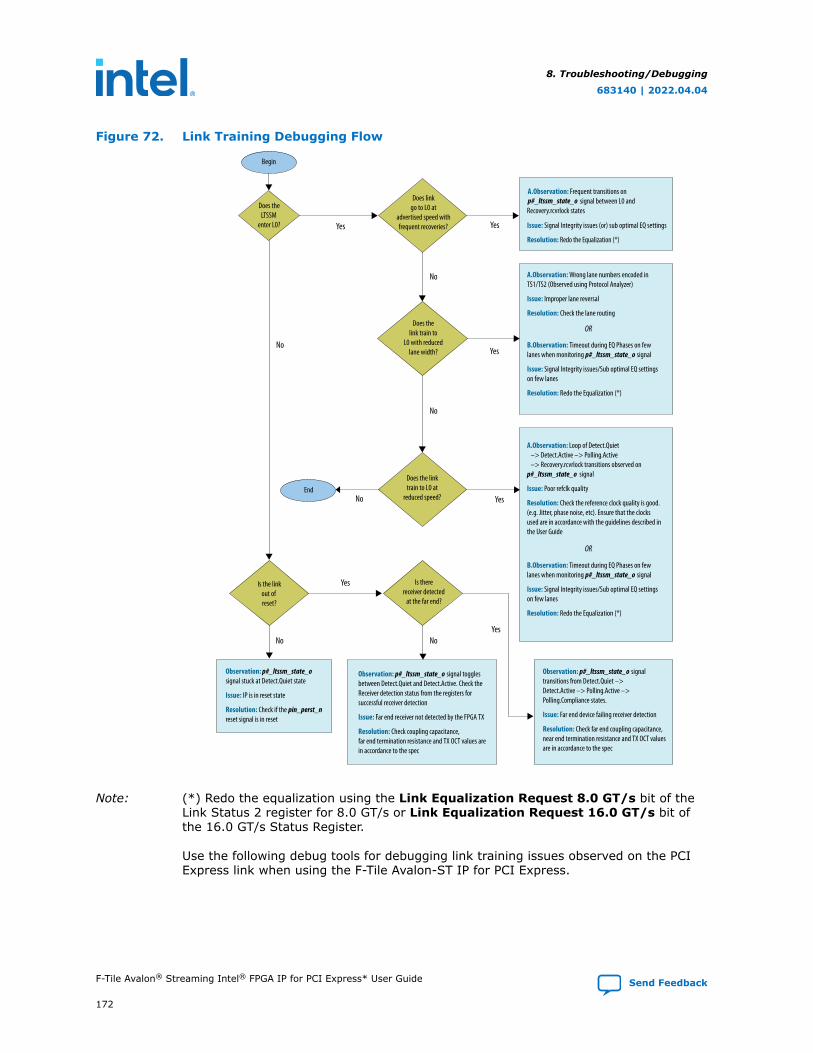
Figure 72. Link Training Debugging Flow
Observation: p#_ltssm_state_o signal toggles between Detect.Quiet and Detect.Active. Check the Receiver detection status from the registers for successful receiver detection
Issue: Far end receiver not detected by the FPGA TX
Resolution: Check coupling capacitance, far end termination resistance and TX OCT values are in accordance to the spec
Observation: p#_ltssm_state_o signal transitions from Detect.Quiet –> Detect.Active –> Polling.Active –> Polling.Compliance states.
Issue: Far end device failing receiver detection
Resolution: Check far end coupling capacitance, near end termination resistance and TX OCT valuesare in accordance to the spec
Observation: signal stuck at Detect.Quiet state
Issue: IP is in reset state
Resolution: Check if the pin_perst_n reset signal is in reset
No
NoNo
Yes
Yes
YesIs the linkout of reset?
Does the linktrain to L0 at
reduced speed?
Is therereceiver detected
at the far end?
A.Observation: Loop of Detect.Quiet –> Detect.Active –> Polling.Active –> Recovery.rcvrlock transitions observed on p#_ltssm_state_o signal
Issue: Poor refclk quality
Resolution: Check the reference clock quality is good. (e.g. Jitter, phase noise, etc). Ensure that the clocks used are in accordance with the guidelines described in the User Guide
B.Observation: Timeout during EQ Phases on few lanes when monitoring p#_ltssm_state_o signal
Issue: Signal Integrity issues/Sub optimal EQ settings on few lanes
Resolution: Redo the Equalization (*)
Yes Yes
No
No
No
Yes
A.Observation: Frequent transitions on p#_ltssm_state_o signal between L0 and Recovery.rcvrlock states
Issue: Signal Integrity issues (or) sub optimal EQ settings
Resolution: Redo the Equalization (*)
A.Observation: Wrong lane numbers encoded in TS1/TS2 (Observed using Protocol Analyzer)
Issue: Improper lane reversal
Resolution: Check the lane routing
B.Observation: Timeout during EQ Phases on few lanes when monitoring p#_ltssm_state_o signal
Issue: Signal Integrity issues/Sub optimal EQ settings on few lanes
Resolution: Redo the Equalization (*)
Begin
OR
OR
Does the LTSSM
enter L0?
Does link go to L0 at
advertised speed with frequent recoveries?
Does the link train to
L0 with reduced lane width?
End
p#_ltssm_state_o
Note: (*) Redo the equalization using the Link Equalization Request 8.0 GT/s bit of theLink Status 2 register for 8.0 GT/s or Link Equalization Request 16.0 GT/s bit ofthe 16.0 GT/s Status Register.
Use the following debug tools for debugging link training issues observed on the PCIExpress link when using the F-Tile Avalon-ST IP for PCI Express.
8. Troubleshooting/Debugging
683140 | 2022.04.04
F-Tile Avalon® Streaming Intel® FPGA IP for PCI Express* User Guide Send Feedback
172
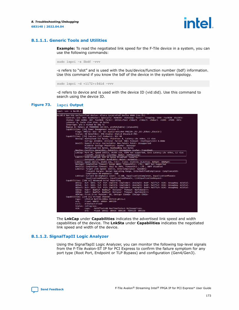
8.1.1.1. Generic Tools and Utilities
Example: To read the negotiated link speed for the F-Tile device in a system, you canuse the following commands:
sudo lspci –s $bdf -vvv
-s refers to “slot” and is used with the bus/device/function number (bdf) information.Use this command if you know the bdf of the device in the system topology.
sudo lspci –d <1172>:$did -vvv
-d refers to device and is used with the device ID (vid:did). Use this command tosearch using the device ID.
Figure 73. lspci Output
The LnkCap under Capabilities indicates the advertised link speed and widthcapabilities of the device. The LnkSta under Capabilities indicates the negotiatedlink speed and width of the device.
8.1.1.2. SignalTapII Logic Analyzer
Using the SignalTapII Logic Analyzer, you can monitor the following top-level signalsfrom the F-Tile Avalon-ST IP for PCI Express to confirm the failure symptom for anyport type (Root Port, Endpoint or TLP Bypass) and configuration (Gen4/Gen3).
8. Troubleshooting/Debugging
683140 | 2022.04.04
Send Feedback F-Tile Avalon® Streaming Intel® FPGA IP for PCI Express* User Guide
173
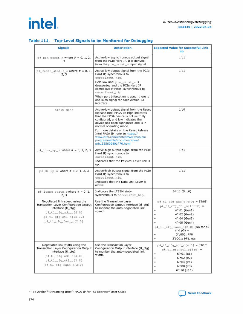
Table 111. Top-Level Signals to be Monitored for Debugging
Signals Description Expected Value for Successful Link-up
p#_pin_perst_n where # = 0, 1, 2,3
Active-low asynchronous output signalfrom the PCIe Hard IP. It is derivedfrom the pin_perst_n input signal.
1'b1
p#_reset_status_n where # = 0, 1,2, 3
Active-low output signal from the PCIeHard IP, synchronous tocoreclkout_hip.Held low until pin_perst_n isdeasserted and the PCIe Hard IPcomes out of reset, synchronous tocoreclkout_hip.When port bifurcation is used, there isone such signal for each Avalon-STinterface.
1'b1
ninit_done Active-low output signal from the ResetRelease Intel FPGA IP. High indicatesthat the FPGA device is not yet fullyconfigured, and low indicates thedevice has been configured and is innormal operating mode.For more details on the Reset ReleaseIntel FPGA IP, refer to https://www.intel.com/content/www/us/en/programmable/documentation/prh1555609801770.html
1'b0
p#_link_up_o where # = 0, 1, 2, 3 Active-high output signal from the PCIeHard IP, synchronous tocoreclkout_hip.Indicates that the Physical Layer link isup.
1'b1
p#_dl_up_o where # = 0, 1, 2, 3 Active-high output signal from the PCIeHard IP, synchronous tocoreclkout_hip.Indicates that the Data Link Layer isactive.
1'b1
p#_ltssm_state_owhere # = 0, 1,2, 3
Indicates the LTSSM state,synchronous to coreclkout_hip.
6'h11 (S_L0)
Negotiated link speed using theTransaction Layer Configuration Output
interface (tl_cfg):p#_tl_cfg_add_o[4:0]
p#_tl_cfg_ctl_o[15:12]
p#_tl_cfg_func_o[2:0]
Use the Transaction LayerConfiguration Output interface (tl_cfg)to monitor the auto-negotiated linkspeed.
p#_tl_cfg_add_o[4:0] = 5'h05p#_tl_cfg_ctl_o[15:12] =
• 4’h01 (Gen1)• 4’h02 (Gen2)• 4’h04 (Gen3)• 4’h08 (Gen4)p#_tl_cfg_func_o[2:0] (NA for p2
and p3) =• 3’b000: PF0• 3'b001: PF1, etc.
Negotiated link width using theTransaction Layer Configuration Output
interface (tl_cfg):p#_tl_cfg_add_o[4:0]
p#_tl_cfg_ctl_o[5:0]
p#_tl_cfg_func_o[2:0]
Use the Transaction LayerConfiguration Output interface (tl_cfg)to monitor the auto-negotiated linkwidth.
p#_tl_cfg_add_o[4:0] = 5'h1Cp#_tl_cfg_ctl_o[5:0] =
• 6’h01 (x1)• 6’h02 (x2)• 6’h04 (x4)• 6’h08 (x8)• 6'h10 (x16)
8. Troubleshooting/Debugging
683140 | 2022.04.04
F-Tile Avalon® Streaming Intel® FPGA IP for PCI Express* User Guide Send Feedback
174
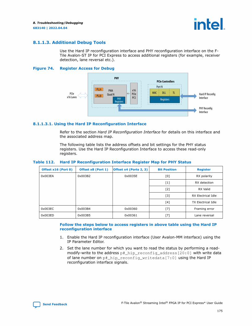
8.1.1.3. Additional Debug Tools
Use the Hard IP reconfiguration interface and PHY reconfiguration interface on the F-Tile Avalon-ST IP for PCI Express to access additional registers (for example, receiverdetection, lane reversal etc.).
Figure 74. Register Access for Debug
PCIe Controllers
Port N
Registers
MACPMA
Quad Nx16PCIePCS
Hard IP ReconfigInterface
PHY ReconfigInterface
PLLAPCIe
x16 Lanes
PHY
PLLBDLL TL
PHYRegisters
8.1.1.3.1. Using the Hard IP Reconfiguration Interface
Refer to the section Hard IP Reconfiguration Interface for details on this interface andthe associated address map.
The following table lists the address offsets and bit settings for the PHY statusregisters. Use the Hard IP Reconfiguration Interface to access these read-onlyregisters.
Table 112. Hard IP Reconfiguration Interface Register Map for PHY Status
Offset x16 (Port 0) Offset x8 (Port 1) Offset x4 (Ports 2, 3) Bit Position Register
0x003EA 0x003B2 0x0035E [0] RX polarity
[1] RX detection
[2] RX Valid
[3] RX Electrical Idle
[4] TX Electrical Idle
0x003EC 0x003B4 0x00360 [7] Framing error
0x003ED 0x003B5 0x00361 [7] Lane reversal
Follow the steps below to access registers in above table using the Hard IPreconfiguration interface
1. Enable the Hard IP reconfiguration interface (User Avalon-MM interface) using theIP Parameter Editor.
2. Set the lane number for which you want to read the status by performing a read-modify-write to the address p#_hip_reconfig_address[20:0] with write dataof lane number on p#_hip_reconfig_writedata[7:0] using the Hard IPreconfiguration interface signals.
8. Troubleshooting/Debugging
683140 | 2022.04.04
Send Feedback F-Tile Avalon® Streaming Intel® FPGA IP for PCI Express* User Guide
175
• p#_hip_reconfig_write = 1’b1
• p#_hip_reconfig_address[20:0] = <offset>
• hip_reconfig_writedata[3:0] = <Lane number>, where Lane number =4’h0 for lane 0, 4’h1 for lane 1, 4’h2 for lane 2, …
3. Read the status of the register you want by performing a read operation from theaddress hip_reconfig_address[20:0] using the Hard IP reconfigurationinterface signals.
• p#_hip_reconfig_read = 1’b1
• p#_hip_reconfig_address[20:0] = <offset>
Offset = Refer to above table for the offset mapping.
• p#_hip_reconfig_readdata[7:0] = Refer to table above for the bitposition mapping.
Example: To read the RX detection status of x16 Port 0 Lane0 using theregisters
1. Enable the Hard IP reconfiguration interface using the IP Parameter Editor.
2. Perform read-modify-write to address 0x0003E8 to set the lane number to 0 usingthe Hard IP reconfiguration interface signals.
• p0_hip_reconfig_write = 1’b1
• p0_hip_reconfig_address[20:0] = 0x003E8
• p0_hip_reconfig_writedata[3:0] = 4'h0
3. Read the status of the RX detection register by performing a read operation fromthe address 0x0003EA[1] using the Hard IP reconfiguration interface signals.
• p0_hip_reconfig_read = 1’b1
• p0_hip_reconfig_address[20:0] = 0x003EA
• p0_hip_reconfig_readdata[1] = 1'b1 (Far end receiver detected)
8.1.1.3.2. Enable and Read LCRC and ECRC Error Count
Table 113. Address Offsets and Bit Settings to enable and read LCRC and ECRC errorcount
OffsetBit Position Register
Offset x16 (Port 0) Offset x8 (Port 1) Offset x4 (Ports 2, 3)
0x00119 0x00119 0x00119 [0] Enable CRC Check
0x0033C 0x00304 0x002B0
[1:0] Event counter clearSet to 2’b01 to clearerror counter definedin registers 0x0033Fand 0x0033ESet to 2’b11 to clearall error counters
[4:2] Event counter enableSet to 3‘b111
continued...
8. Troubleshooting/Debugging
683140 | 2022.04.04
F-Tile Avalon® Streaming Intel® FPGA IP for PCI Express* User Guide Send Feedback
176
OffsetBit Position Register
Offset x16 (Port 0) Offset x8 (Port 1) Offset x4 (Ports 2, 3)
0x0033D 0x00305 0x002B1 [7:0] Event counter laneselectSet to x00
0x0033E 0x00306 0x002B2 [7:0] Event numberFor LCRC error count,set to 0x01For ECRC error count,set to 0x02
0x0033F 0x00307 0x002B3 [7:0] Group numberFor LCRC error count,set to 0x02For ECRC error count,set to 0x03
000x340 0x00308 0x002B4 [7:0] Error counter data bit[7:0]
0x00341 0x00309 0x002B5 [7:0] Error counter data bit[15:8]
0x00342 0x0030A 0x002B6 [7:0] Error counter data bit[23:16]
0x00343 0x0030B 0x002B7 [7:0] Error counter data bit[31:24]
Follow the steps below to access registers in above table using the Hard IPreconfiguration interface
1. Enable the Hard IP reconfiguration interface (User Avalon-MM interface) using theIP Parameter Editor.
2. Enable CRC check by performing a read-modify-write to the addressp#_hip_reconfig_address[20:0] with write data onp#_hip_reconfig_writedata[7:0].
3. Set the group number by performing a read-modify-write to the addressp#_hip_reconfig_address[20:0] with write data onp#_hip_reconfig_writedata[7:0].
4. Set the event number by performing a read-modify-write to the addressp#_hip_reconfig_address[20:0] with write data onp#_hip_reconfig_writedata[7:0].
5. Set the event counter lane select by performing a read-modify-write to theaddress p#_hip_reconfig_address[20:0] with write data onp#_hip_reconfig_writedata[7:0].
6. Set event counter enable by performing a read-modify-write to the addressp#_hip_reconfig_address[20:0] with write data onp#_hip_reconfig_writedata[7:0].
7. Read the error count data by a read operation from the addresship_reconfig_address[20:0].
8. Troubleshooting/Debugging
683140 | 2022.04.04
Send Feedback F-Tile Avalon® Streaming Intel® FPGA IP for PCI Express* User Guide
177
Example: To read the LCRC error count of x16 Port 0 using the registers
1. Enable the Hard IP reconfiguration interface (User Avalon-MM interface) using theIP Parameter Editor.
2. Perform read-modify-write to address 0x00119 to enable CRC check.
• p0_hip_reconfig_write = 1’b1
• p0_hip_reconfig_address[20:0] = 0x00119
• p0_hip_reconfig_writedata[7:0] = 8'h01
3. Perform read-modify-write to address 0x00033F to set Group number.
• p0_hip_reconfig_write = 1’b1
• p0_hip_reconfig_address[20:0] = 0x0033F
• p0_hip_reconfig_writedata[7:0] = 8'h02
4. Perform read-modify-write to address 0x00033E to set Event number.
• p0_hip_reconfig_write = 1’b1
• p0_hip_reconfig_address[20:0] = 0x0033E
• p0_hip_reconfig_writedata[7:0] = 8'h01
5. Perform read-modify-write to address 0x00033D to set Event counter lane select.
• p0_hip_reconfig_write = 1’b1
• p0_hip_reconfig_address[20:0] = 0x0033D
• p0_hip_reconfig_writedata[7:0] = 8'h00
6. Perform read-modify-write to address 0x00033C to set enable event counter.
• p0_hip_reconfig_write = 1’b1
• p0_hip_reconfig_address[20:0] = 0x0033C
• p0_hip_reconfig_writedata[7:0] = 8'h1C
7. Read the error counter data by performing a read operation from registers 0x340,0x341, 0x342, and 0x343.
8.1.2. Debugging Data Transfer and Performance Issues
There are many possible reasons causing the PCIe link to stop transmitting data. ThePCI Express base specification defines three types of errors, outlined in the tablebelow:
Table 114. Error Types Defined by the PCI Express Base Specification
Type Responsible Agent Description
Correctable Hardware While correctable errors may affectsystem performance, data integrity ismaintained.
Uncorrectable, non-fatal Device software Uncorrectable, non-fatal errors aredefined as errors in which data is lost,but system integrity is maintained. For
continued...
8. Troubleshooting/Debugging
683140 | 2022.04.04
F-Tile Avalon® Streaming Intel® FPGA IP for PCI Express* User Guide Send Feedback
178
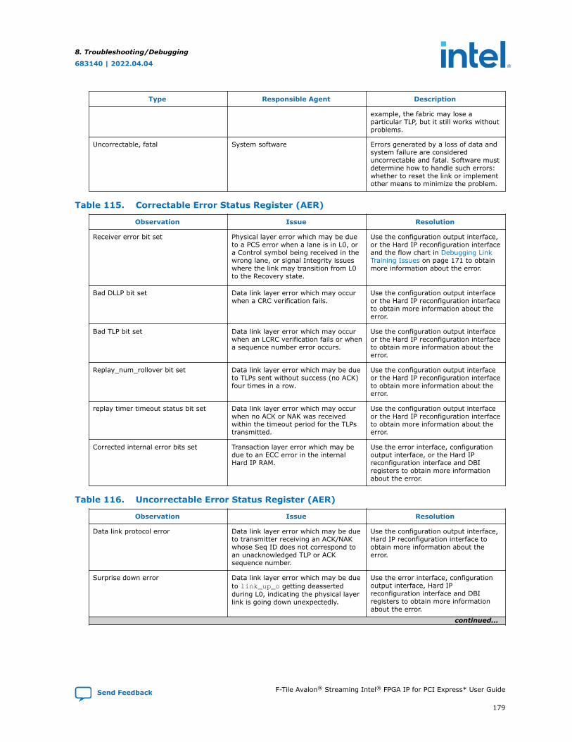
Type Responsible Agent Description
example, the fabric may lose aparticular TLP, but it still works withoutproblems.
Uncorrectable, fatal System software Errors generated by a loss of data andsystem failure are considereduncorrectable and fatal. Software mustdetermine how to handle such errors:whether to reset the link or implementother means to minimize the problem.
Table 115. Correctable Error Status Register (AER)
Observation Issue Resolution
Receiver error bit set Physical layer error which may be dueto a PCS error when a lane is in L0, ora Control symbol being received in thewrong lane, or signal Integrity issueswhere the link may transition from L0to the Recovery state.
Use the configuration output interface,or the Hard IP reconfiguration interfaceand the flow chart in Debugging LinkTraining Issues on page 171 to obtainmore information about the error.
Bad DLLP bit set Data link layer error which may occurwhen a CRC verification fails.
Use the configuration output interfaceor the Hard IP reconfiguration interfaceto obtain more information about theerror.
Bad TLP bit set Data link layer error which may occurwhen an LCRC verification fails or whena sequence number error occurs.
Use the configuration output interfaceor the Hard IP reconfiguration interfaceto obtain more information about theerror.
Replay_num_rollover bit set Data link layer error which may be dueto TLPs sent without success (no ACK)four times in a row.
Use the configuration output interfaceor the Hard IP reconfiguration interfaceto obtain more information about theerror.
replay timer timeout status bit set Data link layer error which may occurwhen no ACK or NAK was receivedwithin the timeout period for the TLPstransmitted.
Use the configuration output interfaceor the Hard IP reconfiguration interfaceto obtain more information about theerror.
Corrected internal error bits set Transaction layer error which may bedue to an ECC error in the internalHard IP RAM.
Use the error interface, configurationoutput interface, or the Hard IPreconfiguration interface and DBIregisters to obtain more informationabout the error.
Table 116. Uncorrectable Error Status Register (AER)
Observation Issue Resolution
Data link protocol error Data link layer error which may be dueto transmitter receiving an ACK/NAKwhose Seq ID does not correspond toan unacknowledged TLP or ACKsequence number.
Use the configuration output interface,Hard IP reconfiguration interface toobtain more information about theerror.
Surprise down error Data link layer error which may be dueto link_up_o getting deassertedduring L0, indicating the physical layerlink is going down unexpectedly.
Use the error interface, configurationoutput interface, Hard IPreconfiguration interface and DBIregisters to obtain more informationabout the error.
continued...
8. Troubleshooting/Debugging
683140 | 2022.04.04
Send Feedback F-Tile Avalon® Streaming Intel® FPGA IP for PCI Express* User Guide
179
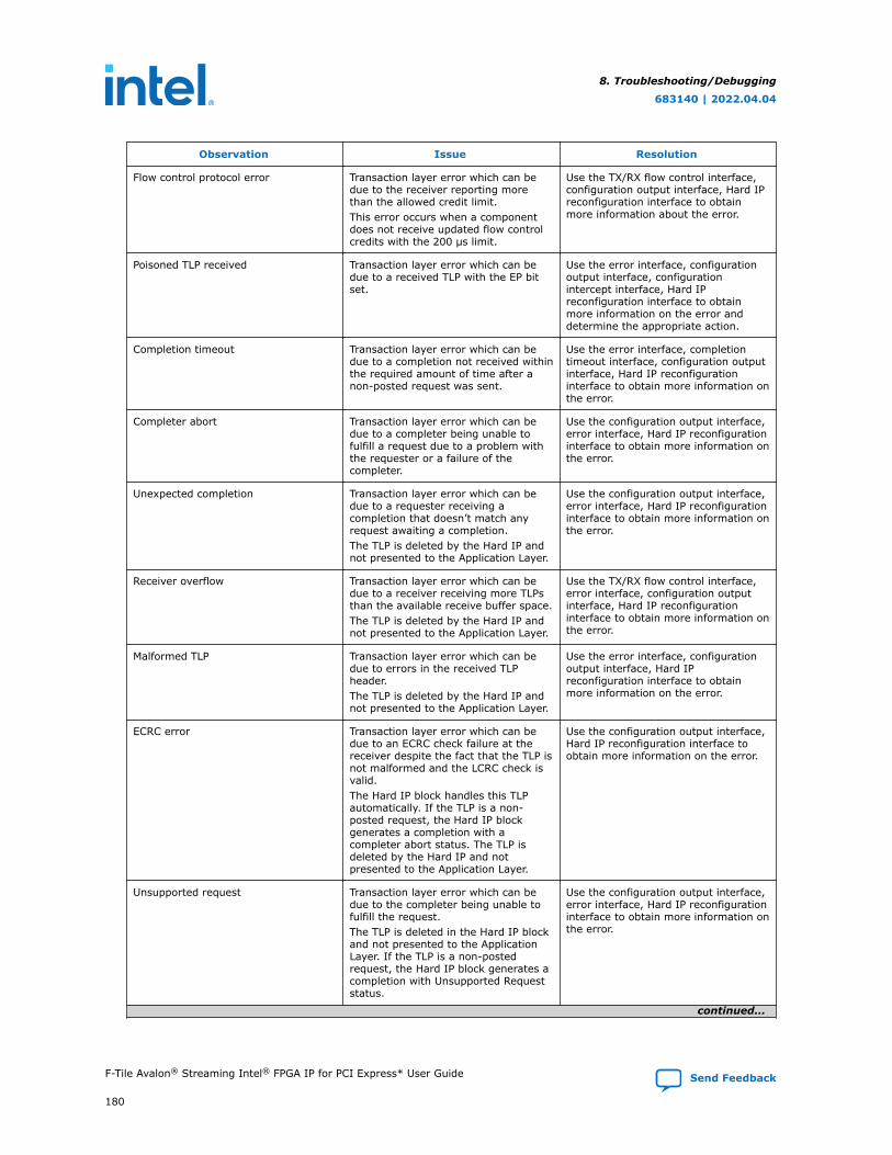
Observation Issue Resolution
Flow control protocol error Transaction layer error which can bedue to the receiver reporting morethan the allowed credit limit.This error occurs when a componentdoes not receive updated flow controlcredits with the 200 μs limit.
Use the TX/RX flow control interface,configuration output interface, Hard IPreconfiguration interface to obtainmore information about the error.
Poisoned TLP received Transaction layer error which can bedue to a received TLP with the EP bitset.
Use the error interface, configurationoutput interface, configurationintercept interface, Hard IPreconfiguration interface to obtainmore information on the error anddetermine the appropriate action.
Completion timeout Transaction layer error which can bedue to a completion not received withinthe required amount of time after anon-posted request was sent.
Use the error interface, completiontimeout interface, configuration outputinterface, Hard IP reconfigurationinterface to obtain more information onthe error.
Completer abort Transaction layer error which can bedue to a completer being unable tofulfill a request due to a problem withthe requester or a failure of thecompleter.
Use the configuration output interface,error interface, Hard IP reconfigurationinterface to obtain more information onthe error.
Unexpected completion Transaction layer error which can bedue to a requester receiving acompletion that doesn’t match anyrequest awaiting a completion.The TLP is deleted by the Hard IP andnot presented to the Application Layer.
Use the configuration output interface,error interface, Hard IP reconfigurationinterface to obtain more information onthe error.
Receiver overflow Transaction layer error which can bedue to a receiver receiving more TLPsthan the available receive buffer space.The TLP is deleted by the Hard IP andnot presented to the Application Layer.
Use the TX/RX flow control interface,error interface, configuration outputinterface, Hard IP reconfigurationinterface to obtain more information onthe error.
Malformed TLP Transaction layer error which can bedue to errors in the received TLPheader.The TLP is deleted by the Hard IP andnot presented to the Application Layer.
Use the error interface, configurationoutput interface, Hard IPreconfiguration interface to obtainmore information on the error.
ECRC error Transaction layer error which can bedue to an ECRC check failure at thereceiver despite the fact that the TLP isnot malformed and the LCRC check isvalid.The Hard IP block handles this TLPautomatically. If the TLP is a non-posted request, the Hard IP blockgenerates a completion with acompleter abort status. The TLP isdeleted by the Hard IP and notpresented to the Application Layer.
Use the configuration output interface,Hard IP reconfiguration interface toobtain more information on the error.
Unsupported request Transaction layer error which can bedue to the completer being unable tofulfill the request.The TLP is deleted in the Hard IP blockand not presented to the ApplicationLayer. If the TLP is a non-postedrequest, the Hard IP block generates acompletion with Unsupported Requeststatus.
Use the configuration output interface,error interface, Hard IP reconfigurationinterface to obtain more information onthe error.
continued...
8. Troubleshooting/Debugging
683140 | 2022.04.04
F-Tile Avalon® Streaming Intel® FPGA IP for PCI Express* User Guide Send Feedback
180
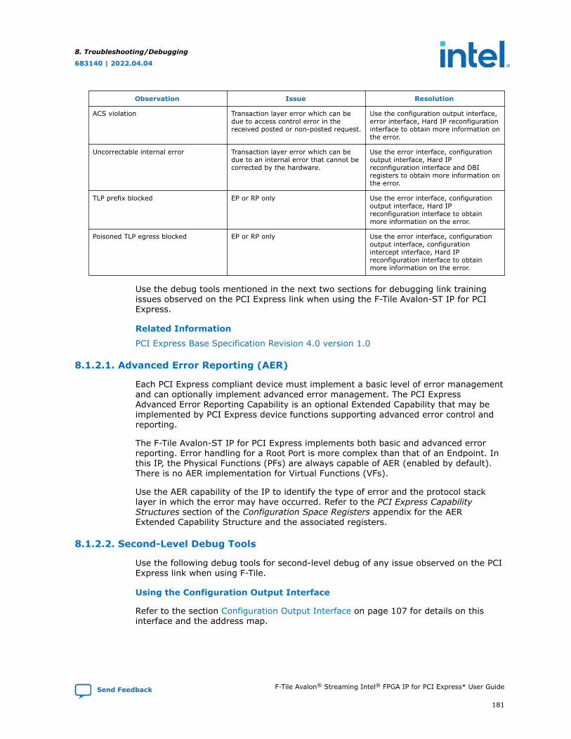
Observation Issue Resolution
ACS violation Transaction layer error which can bedue to access control error in thereceived posted or non-posted request.
Use the configuration output interface,error interface, Hard IP reconfigurationinterface to obtain more information onthe error.
Uncorrectable internal error Transaction layer error which can bedue to an internal error that cannot becorrected by the hardware.
Use the error interface, configurationoutput interface, Hard IPreconfiguration interface and DBIregisters to obtain more information onthe error.
TLP prefix blocked EP or RP only Use the error interface, configurationoutput interface, Hard IPreconfiguration interface to obtainmore information on the error.
Poisoned TLP egress blocked EP or RP only Use the error interface, configurationoutput interface, configurationintercept interface, Hard IPreconfiguration interface to obtainmore information on the error.
Use the debug tools mentioned in the next two sections for debugging link trainingissues observed on the PCI Express link when using the F-Tile Avalon-ST IP for PCIExpress.
Related Information
PCI Express Base Specification Revision 4.0 version 1.0
8.1.2.1. Advanced Error Reporting (AER)
Each PCI Express compliant device must implement a basic level of error managementand can optionally implement advanced error management. The PCI ExpressAdvanced Error Reporting Capability is an optional Extended Capability that may beimplemented by PCI Express device functions supporting advanced error control andreporting.
The F-Tile Avalon-ST IP for PCI Express implements both basic and advanced errorreporting. Error handling for a Root Port is more complex than that of an Endpoint. Inthis IP, the Physical Functions (PFs) are always capable of AER (enabled by default).There is no AER implementation for Virtual Functions (VFs).
Use the AER capability of the IP to identify the type of error and the protocol stacklayer in which the error may have occurred. Refer to the PCI Express CapabilityStructures section of the Configuration Space Registers appendix for the AERExtended Capability Structure and the associated registers.
8.1.2.2. Second-Level Debug Tools
Use the following debug tools for second-level debug of any issue observed on the PCIExpress link when using F-Tile.
Using the Configuration Output Interface
Refer to the section Configuration Output Interface on page 107 for details on thisinterface and the address map.
8. Troubleshooting/Debugging
683140 | 2022.04.04
Send Feedback F-Tile Avalon® Streaming Intel® FPGA IP for PCI Express* User Guide
181
Using the Error Interface
Refer to the section Error Interface on page 98 for details on this interface and theaddress map.
Using the Configuration Intercept Interface
Refer to the section Configuration Intercept Interface (EP Only) on page 108 fordetails on this interface and the address map.
Using the TX/RX Flow Control
Refer to the sections TX Flow Control on page 32 and RX Flow Control on page 29 fordetails on these interfaces and their address maps.
Using the Hard IP Reconfiguration Interface
Refer to the section Hard IP Reconfiguration Interface on page 110 for details on thisinterface and the address map.
Using the PHY Reconfiguration Interface
Refer to the section PHY Reconfiguration Interface on page 111 for details on thisinterface and the address map.
8.2. Debug Toolkit
8.2.1. Overview
The F-Tile Debug Toolkit is a System Console-based tool for F-Tile that provides real-time control, monitoring and debugging of the PCIe links at the Physical Layer.
The F-Tile Debug Toolkit allows you to:
• View protocol and link status of the PCIe links.
• View PLL and per-channel status of the PCIe links.
• View the channel analog settings.
• Indicate the presence of a re-timer connected between the link partners.
Note: The current version of Intel Quartus Prime supports enabling the Debug Toolkit for theEndpoint mode only, and with the Linux and Windows operating systems only.
The following figure provides an overview of the F-Tile Debug Toolkit in the F-TileAvalon-ST IP for PCI Express.
8. Troubleshooting/Debugging
683140 | 2022.04.04
F-Tile Avalon® Streaming Intel® FPGA IP for PCI Express* User Guide Send Feedback
182
Figure 75. Overview of the F-Tile Debug Toolkit
F-Tile Debug Toolkit
NPDME
hip-reconfig_*
intel_pcie_ftile_ast
AVMMPCle Config Space Registers
(Port 0)
AVMMPCle Config Space Registers
(Port 3)
AVMM PHY Registers (Quad 0)
AVMM PHY Registers (Quad 3)
...
...
System Console
GUI
xcvr_reconfig_*
When you enable the F-Tile Debug Toolkit, the intel_pcie_ftile_ast module ofthe generated IP includes the Debug Toolkit modules and related logic as shown in thefigure above.
Drive the Debug Toolkit from a System Console. The System Console connects to theDebug Toolkit via an Native PHY Debug Master Endpoint (NPDME). Make thisconnection via an Intel FPGA Download Cable.
The PHY reconfiguration interface clock (xcvr_reconfig_clk) is used to clock thefollowing interfaces:
• The NPDME module
• PHY reconfiguration interface (xcvr_reconfig)
• Hard IP reconfiguration interface (hip_reconfig)
Provide a clock source (50 MHz - 125 MHz, 100 MHz recommended clock frequency) todrive the xcvr_reconfig_clk clock. Use the output of the Reset Release Intel FPGAIP to drive the ninit_done, which provides the reset signal to the NPDME module.
Note: When you enable the F-Tile Debug Toolkit, the Hard IP Reconfiguration interface isenabled by default.
When you run a dynamically-generated design example on the Intel Development Kit,make sure that clock and reset signals are connected to their respective sources andappropriate pin assignments are made. Here are some sample .qsf assignments forthe Debug Toolkit:
• set_location_assignment PIN_C23 -to xcvr_reconfig_clk_clk
8. Troubleshooting/Debugging
683140 | 2022.04.04
Send Feedback F-Tile Avalon® Streaming Intel® FPGA IP for PCI Express* User Guide
183
8.2.2. Enabling the F-Tile Debug Toolkit
To enable the F-Tile Debug Toolkit in your design, enable the option Enable ftileDebug Toolkit in the Top-Level Settings options tab of the Intel FPGA F-TileAvalon-ST IP for PCI Express.
You must also enable the option Enable PHY reconfiguration interface for theDebug Toolkit to function as expected.
Note: When you enable the F-Tile Debug Toolkit in the IP, the Hard IP reconfigurationinterface and the PHY reconfiguration interface will be used by the Debug Toolkit.Hence, you will not be able to drive logic on these interfaces from the FPGA fabric.
8.2.3. Launching the F-Tile Debug Toolkit
Use the design example you compiled by following the Quick Start Guide to familiarizeyourself with the F-Tile Debug Toolkit. Follow the steps in the Generating the DesignExample and Compiling the Design Example to generate the SRAM Object File, (.sof)for this design example.
To use the F-Tile Debug Toolkit, download the .sof to the Intel Development Kit. Then,open the System Console and load the design to the System Console as well. Loadingthe .sof to the System Console allows the System Console to communicate with thedesign using NPDME. NPDME is a JTAG-based Avalon-MM master. It drives Avalon-MMslave interfaces in the PCIe design. When using NPDME, the Intel Quartus Primesoftware inserts the debug interconnect fabric to connect with JTAG.
Here are the steps to complete these tasks:
1. Use the Intel Quartus Prime Programmer to download the .sof to the Intel FPGADevelopment Kit.
Note: To ensure correct operation, use the same version of the Intel QuartusPrime Programmer and Intel Quartus Prime Pro Edition software that youused to generate the .sof.
2. To load the design into System Console:
a. Launch the Intel Quartus Prime Pro Edition software.
b. Start System Console by choosing Tools, then System Debugging Tools,then System Console.
c. On the System Console File menu, select Load design and browse to the .soffile.
8. Troubleshooting/Debugging
683140 | 2022.04.04
F-Tile Avalon® Streaming Intel® FPGA IP for PCI Express* User Guide Send Feedback
184
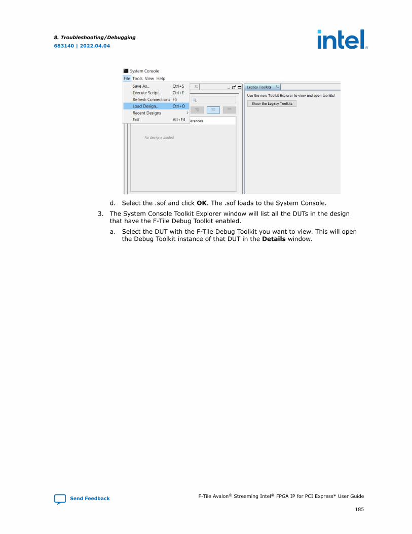
d. Select the .sof and click OK. The .sof loads to the System Console.
3. The System Console Toolkit Explorer window will list all the DUTs in the designthat have the F-Tile Debug Toolkit enabled.
a. Select the DUT with the F-Tile Debug Toolkit you want to view. This will openthe Debug Toolkit instance of that DUT in the Details window.
8. Troubleshooting/Debugging
683140 | 2022.04.04
Send Feedback F-Tile Avalon® Streaming Intel® FPGA IP for PCI Express* User Guide
185
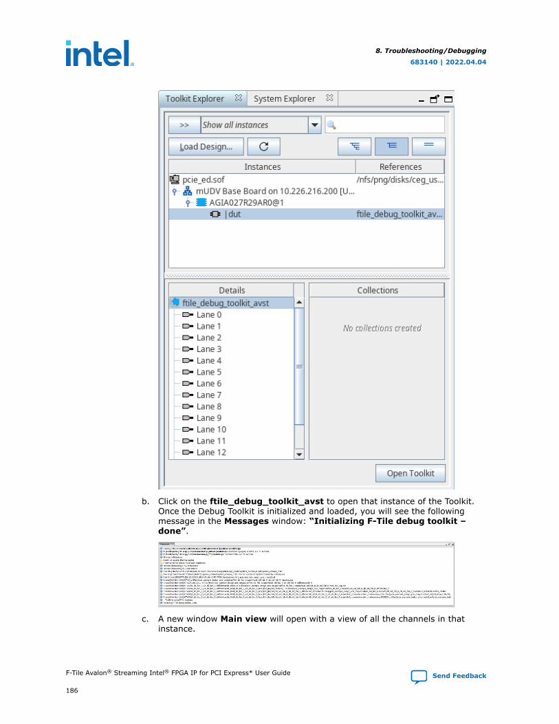
b. Click on the ftile_debug_toolkit_avst to open that instance of the Toolkit.Once the Debug Toolkit is initialized and loaded, you will see the followingmessage in the Messages window: “Initializing F-Tile debug toolkit –done”.
c. A new window Main view will open with a view of all the channels in thatinstance.
8. Troubleshooting/Debugging
683140 | 2022.04.04
F-Tile Avalon® Streaming Intel® FPGA IP for PCI Express* User Guide Send Feedback
186
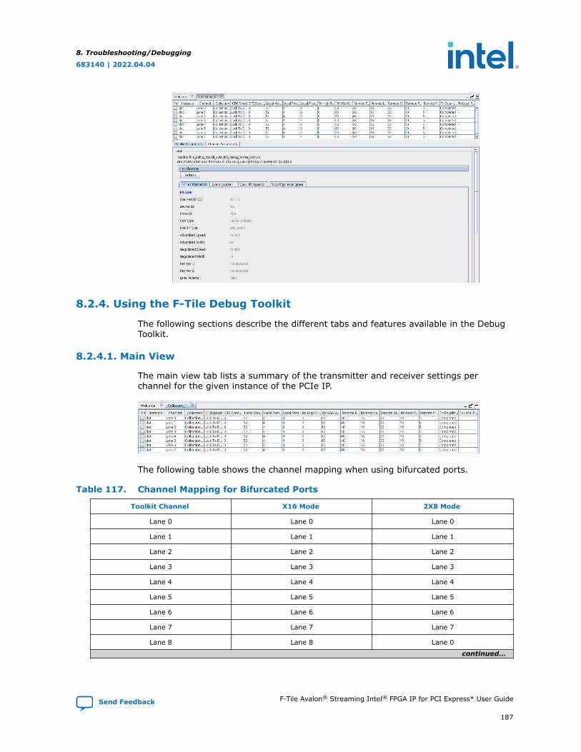
8.2.4. Using the F-Tile Debug Toolkit
The following sections describe the different tabs and features available in the DebugToolkit.
8.2.4.1. Main View
The main view tab lists a summary of the transmitter and receiver settings perchannel for the given instance of the PCIe IP.
The following table shows the channel mapping when using bifurcated ports.
Table 117. Channel Mapping for Bifurcated Ports
Toolkit Channel X16 Mode 2X8 Mode
Lane 0 Lane 0 Lane 0
Lane 1 Lane 1 Lane 1
Lane 2 Lane 2 Lane 2
Lane 3 Lane 3 Lane 3
Lane 4 Lane 4 Lane 4
Lane 5 Lane 5 Lane 5
Lane 6 Lane 6 Lane 6
Lane 7 Lane 7 Lane 7
Lane 8 Lane 8 Lane 0
continued...
8. Troubleshooting/Debugging
683140 | 2022.04.04
Send Feedback F-Tile Avalon® Streaming Intel® FPGA IP for PCI Express* User Guide
187
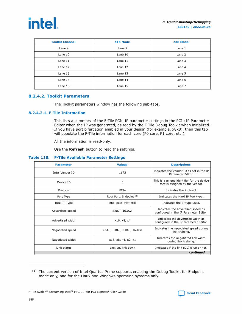
Toolkit Channel X16 Mode 2X8 Mode
Lane 9 Lane 9 Lane 1
Lane 10 Lane 10 Lane 2
Lane 11 Lane 11 Lane 3
Lane 12 Lane 12 Lane 4
Lane 13 Lane 13 Lane 5
Lane 14 Lane 14 Lane 6
Lane 15 Lane 15 Lane 7
8.2.4.2. Toolkit Parameters
The Toolkit parameters window has the following sub-tabs.
8.2.4.2.1. F-Tile Information
This lists a summary of the F-Tile PCIe IP parameter settings in the PCIe IP ParameterEditor when the IP was generated, as read by the F-Tile Debug Toolkit when initialized.If you have port bifurcation enabled in your design (for example, x8x8), then this tabwill populate the F-Tile information for each core (P0 core, P1 core, etc.).
All the information is read-only.
Use the Refresh button to read the settings.
Table 118. F-Tile Available Parameter Settings
Parameter Values Descriptions
Intel Vendor ID 1172 Indicates the Vendor ID as set in the IPParameter Editor.
Device ID 0 This is a unique identifier for the devicethat is assigned by the vendor.
Protocol PCIe Indicates the Protocol.
Port Type Root Port, Endpoint (1) Indicates the Hard IP Port type.
Intel IP Type intel_pcie_avst_ftile Indicates the IP type used.
Advertised speed 8.0GT, 16.0GT Indicates the advertised speed asconfigured in the IP Parameter Editor.
Advertised width x16, x8, x4 Indicates the advertised width asconfigured in the IP Parameter Editor.
Negotiated speed 2.5GT, 5.0GT, 8.0GT, 16.0GT Indicates the negotiated speed duringlink training.
Negotiated width x16, x8, x4, x2, x1 Indicates the negotiated link widthduring link training.
Link status Link up, link down Indicates if the link (DL) is up or not.
continued...
(1) The current version of Intel Quartus Prime supports enabling the Debug Toolkit for Endpointmode only, and for the Linux and Windows operating systems only.
8. Troubleshooting/Debugging
683140 | 2022.04.04
F-Tile Avalon® Streaming Intel® FPGA IP for PCI Express* User Guide Send Feedback
188
Parameter Values Descriptions
LTSSM State Refer to Hard IP Status Interface onpage 97 Indicates the current state of the link.
Lane Reversal True, False Indicates if lane reversal happens onthe link.
Retimer 1 Detected, not detectedIndicates if a retimer was detected
between the Root Port and theEndpoint.
Retimer 2 Detected, not detectedIndicates if a retimer was detected
between the Root Port and theEndpoint.
Tx TLP Sequence Number Hexadecimal value Indicates the next transmit sequencenumber for the transmit TLP.
Tx Ack Sequence Timeout Hexadecimal valueIndicates the ACK sequence number
which is updated by receiving ACK/NAKDLLP.
Replay Timer Timeout Green, RedGreen: no timeout
Red: timeout
Malformed TLP Status Green, RedGreen: no malformed TLP
Red: malformed TLP detected
First Malformed TLP Error Pointer
• AtomicOp address alignment• AtomicOp operand• AtomicOp byte enable• TLP length mismatch• Max payload size• Message TLP without TC0• Invalid TC• Unexpected route bit in Message
TLP• Unexpected CRS status in
Completion TLP• Byte enable• Memory address 4KB boundary• TLP prefix rules• Translation request rules• Invalid TLP type• Completion rules• Application
PIPE PhyStatus 0/1
Indicates the PMA and PCS are in resetmode.
0: PMA and PCS are out of reset1: PMA and PCS are in reset
8. Troubleshooting/Debugging
683140 | 2022.04.04
Send Feedback F-Tile Avalon® Streaming Intel® FPGA IP for PCI Express* User Guide
189
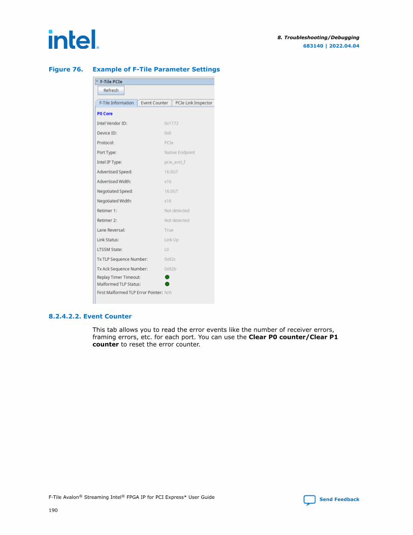
Figure 76. Example of F-Tile Parameter Settings
8.2.4.2.2. Event Counter
This tab allows you to read the error events like the number of receiver errors,framing errors, etc. for each port. You can use the Clear P0 counter/Clear P1counter to reset the error counter.
8. Troubleshooting/Debugging
683140 | 2022.04.04
F-Tile Avalon® Streaming Intel® FPGA IP for PCI Express* User Guide Send Feedback
190
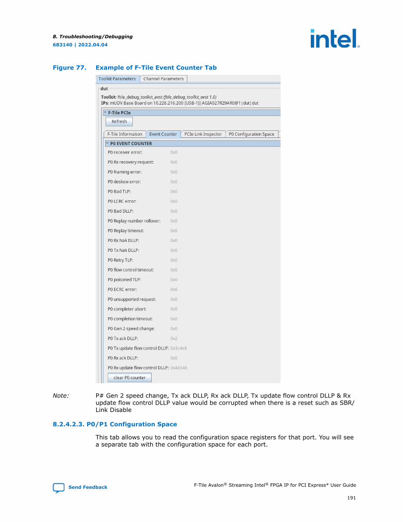
Figure 77. Example of F-Tile Event Counter Tab
Note: P# Gen 2 speed change, Tx ack DLLP, Rx ack DLLP, Tx update flow control DLLP & Rxupdate flow control DLLP value would be corrupted when there is a reset such as SBR/Link Disable
8.2.4.2.3. P0/P1 Configuration Space
This tab allows you to read the configuration space registers for that port. You will seea separate tab with the configuration space for each port.
8. Troubleshooting/Debugging
683140 | 2022.04.04
Send Feedback F-Tile Avalon® Streaming Intel® FPGA IP for PCI Express* User Guide
191
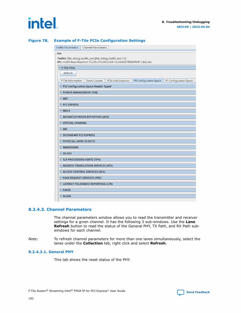
Figure 78. Example of F-Tile PCIe Configuration Settings
8.2.4.3. Channel Parameters
The channel parameters window allows you to read the transmitter and receiversettings for a given channel. It has the following 3 sub-windows. Use the LaneRefresh button to read the status of the General PHY, TX Path, and RX Path sub-windows for each channel.
Note: To refresh channel parameters for more than one lanes simultaneously, select thelanes under the Collection tab, right click and select Refresh.
8.2.4.3.1. General PHY
This tab shows the reset status of the PHY.
8. Troubleshooting/Debugging
683140 | 2022.04.04
F-Tile Avalon® Streaming Intel® FPGA IP for PCI Express* User Guide Send Feedback
192
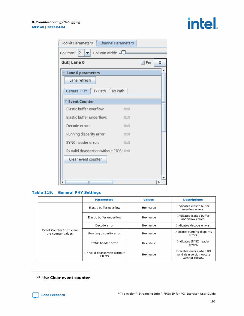
Table 119. General PHY Settings
Parameters Values Descriptions
Event Counter (2) to clearthe counter values.
Elastic buffer overflow Hex value Indicates elastic bufferoverflow errors.
Elastic buffer underflow Hex value Indicates elastic bufferunderflow errors.
Decode error Hex value Indicates decode errors.
Running disparity error Hex value Indicates running disparityerrors.
SYNC header error Hex value Indicates SYNC headererrors.
RX valid deassertion withoutEIEOS Hex value
Indicates errors when RXvalid deassertion occurs
without EIEOS.
(2) Use Clear event counter
8. Troubleshooting/Debugging
683140 | 2022.04.04
Send Feedback F-Tile Avalon® Streaming Intel® FPGA IP for PCI Express* User Guide
193
8.2.4.3.2. TX Path
This tab allows you to monitor the transmitter settings for the channel selected.
Table 120. Transmitter Settings
Parameters Values Descriptions
TX Status TX Electrical Idle True, False
Indicates if TX is in electricalidle.
True: indicates TX is inelectrical idle.
False: indicates TX is out ofelectrical idle.
TX PLL TX PLL lock Green, RedIndicates if TX PLL is locked.
Green: TX PLL is locked.Red: TX PLL is not locked.
TX Equalization
TX Equalization Status Not attempted, Completed,Unsuccessful
Indicates transmitterequalization status. The TX
local and remote parametersare valid only when the
value of Equalization statusis returned as completed,indicating equalization has
completed successfully.
TX Local Preset P0 to P10
Indicates the F-tiletransmitter driver presetvalue as requested by the
link partner during theEqualization phase of link
training. If the preset is notone of these values, then no
value is shown.
Local Pre-shoot coefficientDepends on the coefficient
requested by the linkpartner.
Indicates F-tile transmitterdriver output pre-emphasis
(pre-cursor coefficientvalue).
Local main coefficientDepends on the coefficient
requested by the linkpartner.
Indicates F-tile transmitterdriver output pre-emphasis
(main cursor coefficientvalue).
Local post coefficientDepends on the coefficient
requested by the linkpartner.
Indicates F-tile transmitterdriver output pre-emphasis
(post-cursor coefficientvalue).
Remote Pre-shoot coefficient(†)
Depends on the transmitterdriver output of the link
partner.
Indicates link partner'stransmitter driver's output
pre-cursor coefficient value,as received by F-tile duringthe Equalization phase of
link training. When F-tile isconfigured in Endpoint
mode, this valuecorresponds to the
coefficient received duringPhase 2 of Equalization.
Remote main coefficient (†)Depends on the transmitter
driver output of the linkpartner.
Indicates link partner'stransmitter driver's output
main cursor coefficientvalue, as received by F-Tile
during the Equalization
continued...
8. Troubleshooting/Debugging
683140 | 2022.04.04
F-Tile Avalon® Streaming Intel® FPGA IP for PCI Express* User Guide Send Feedback
194
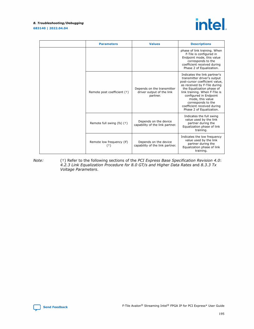
Parameters Values Descriptions
phase of link training. WhenF-Tile is configured in
Endpoint mode, this valuecorresponds to the
coefficient received duringPhase 2 of Equalization.
Remote post coefficient (†)Depends on the transmitter
driver output of the linkpartner.
Indicates the link partner'stransmitter driver's output
post-cursor coefficient value,as received by F-Tile duringthe Equalization phase of
link training. When F-Tile isconfigured in Endpoint
mode, this valuecorresponds to the
coefficient received duringPhase 2 of Equalization.
Remote full swing (fs) (†) Depends on the devicecapability of the link partner.
Indicates the full swingvalue used by the link
partner during theEqualization phase of link
training.
Remote low frequency (lf)(†)
Depends on the devicecapability of the link partner.
Indicates the low frequencyvalue used by the link
partner during theEqualization phase of link
training.
Note: (†) Refer to the following sections of the PCI Express Base Specification Revision 4.0:4.2.3 Link Equalization Procedure for 8.0 GT/s and Higher Data Rates and 8.3.3 TxVoltage Parameters.
8. Troubleshooting/Debugging
683140 | 2022.04.04
Send Feedback F-Tile Avalon® Streaming Intel® FPGA IP for PCI Express* User Guide
195
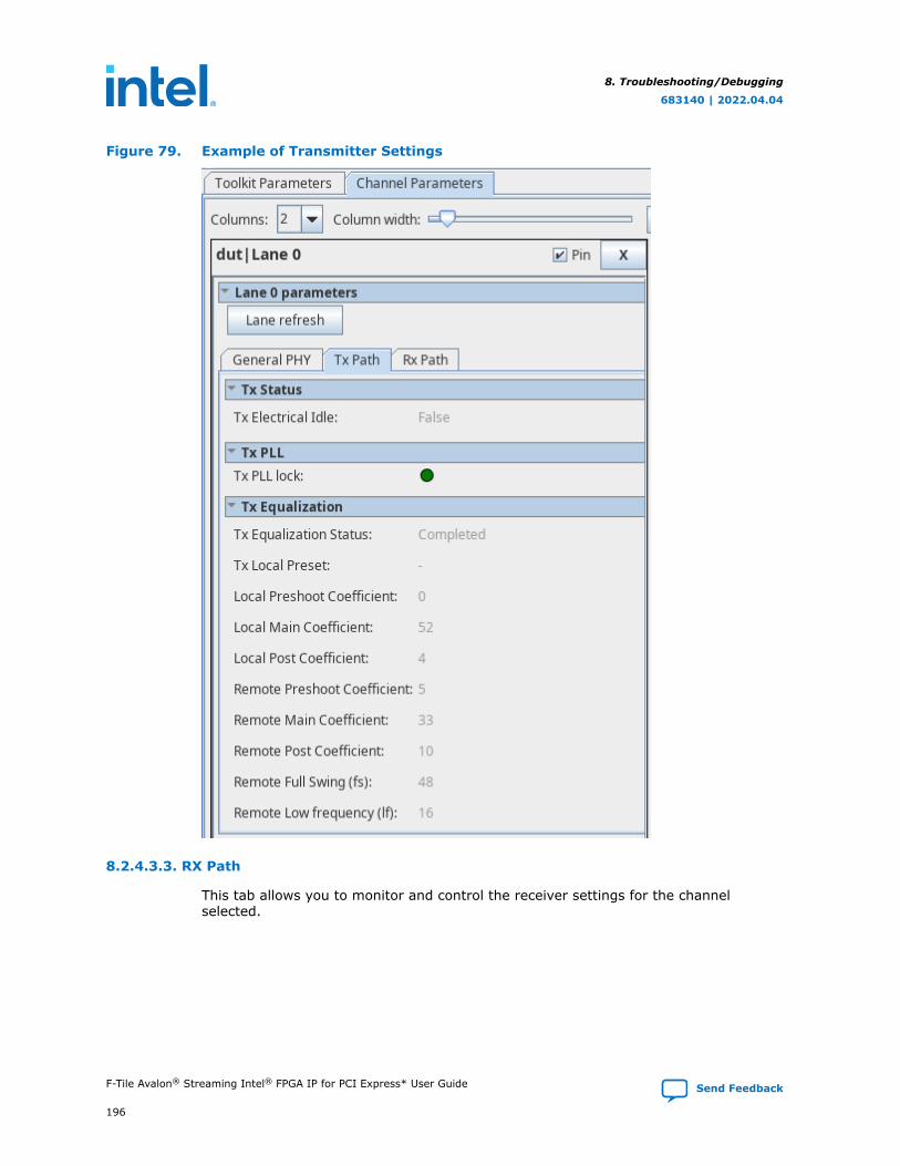
Figure 79. Example of Transmitter Settings
8.2.4.3.3. RX Path
This tab allows you to monitor and control the receiver settings for the channelselected.
8. Troubleshooting/Debugging
683140 | 2022.04.04
F-Tile Avalon® Streaming Intel® FPGA IP for PCI Express* User Guide Send Feedback
196
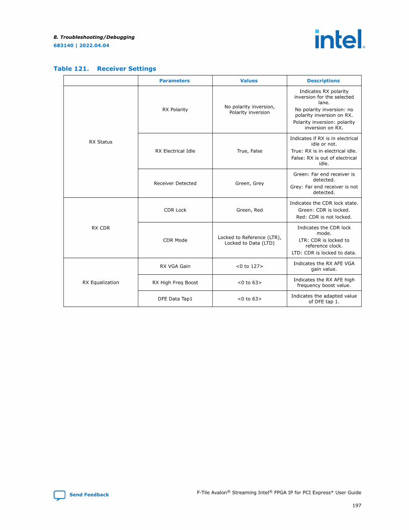
Table 121. Receiver Settings
Parameters Values Descriptions
RX Status
RX Polarity No polarity inversion,Polarity inversion
Indicates RX polarityinversion for the selected
lane.No polarity inversion: nopolarity inversion on RX.
Polarity inversion: polarityinversion on RX.
RX Electrical Idle True, False
Indicates if RX is in electricalidle or not.
True: RX is in electrical idle.False: RX is out of electrical
idle.
Receiver Detected Green, Grey
Green: Far end receiver isdetected.
Grey: Far end receiver is notdetected.
RX CDR
CDR Lock Green, RedIndicates the CDR lock state.
Green: CDR is locked.Red: CDR is not locked.
CDR Mode Locked to Reference (LTR),Locked to Data (LTD)
Indicates the CDR lockmode.
LTR: CDR is locked toreference clock.
LTD: CDR is locked to data.
RX Equalization
RX VGA Gain <0 to 127> Indicates the RX AFE VGAgain value.
RX High Freq Boost <0 to 63> Indicates the RX AFE highfrequency boost value.
DFE Data Tap1 <0 to 63> Indicates the adapted valueof DFE tap 1.
8. Troubleshooting/Debugging
683140 | 2022.04.04
Send Feedback F-Tile Avalon® Streaming Intel® FPGA IP for PCI Express* User Guide
197
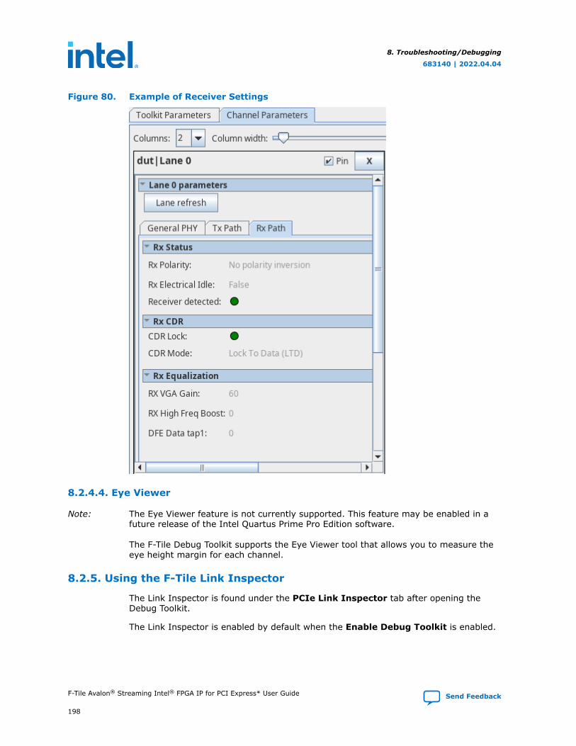
Figure 80. Example of Receiver Settings
8.2.4.4. Eye Viewer
Note: The Eye Viewer feature is not currently supported. This feature may be enabled in afuture release of the Intel Quartus Prime Pro Edition software.
The F-Tile Debug Toolkit supports the Eye Viewer tool that allows you to measure theeye height margin for each channel.
8.2.5. Using the F-Tile Link Inspector
The Link Inspector is found under the PCIe Link Inspector tab after opening theDebug Toolkit.
The Link Inspector is enabled by default when the Enable Debug Toolkit is enabled.
8. Troubleshooting/Debugging
683140 | 2022.04.04
F-Tile Avalon® Streaming Intel® FPGA IP for PCI Express* User Guide Send Feedback
198
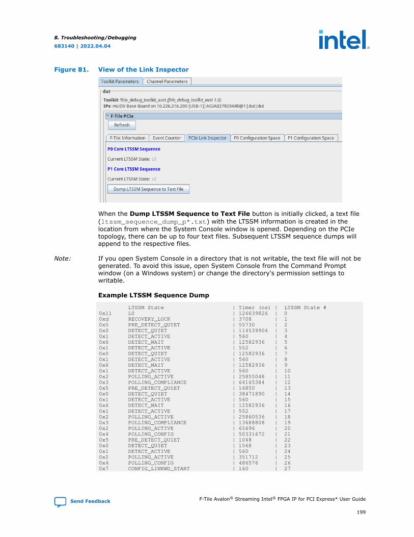
Figure 81. View of the Link Inspector
When the Dump LTSSM Sequence to Text File button is initially clicked, a text file(ltssm_sequence_dump_p*.txt) with the LTSSM information is created in thelocation from where the System Console window is opened. Depending on the PCIetopology, there can be up to four text files. Subsequent LTSSM sequence dumps willappend to the respective files.
Note: If you open System Console in a directory that is not writable, the text file will not begenerated. To avoid this issue, open System Console from the Command Promptwindow (on a Windows system) or change the directory's permission settings towritable.
Example LTSSM Sequence Dump
LTSSM State | Timer (ns) | LTSSM State #0x11 L0 | 126639826 | 0 0xd RECOVERY_LOCK | 3708 | 1 0x5 PRE_DETECT_QUIET | 55730 | 2 0x0 DETECT_QUIET | 114539904 | 3 0x1 DETECT_ACTIVE | 560 | 4 0x6 DETECT_WAIT | 12582936 | 5 0x1 DETECT_ACTIVE | 552 | 6 0x0 DETECT_QUIET | 12582936 | 7 0x1 DETECT_ACTIVE | 560 | 8 0x6 DETECT_WAIT | 12582936 | 9 0x1 DETECT_ACTIVE | 560 | 10 0x2 POLLING_ACTIVE | 25855048 | 11 0x3 POLLING_COMPLIANCE | 64165384 | 12 0x5 PRE_DETECT_QUIET | 16850 | 13 0x0 DETECT_QUIET | 38471890 | 14 0x1 DETECT_ACTIVE | 560 | 15 0x6 DETECT_WAIT | 12582936 | 16 0x1 DETECT_ACTIVE | 552 | 17 0x2 POLLING_ACTIVE | 25860536 | 18 0x3 POLLING_COMPLIANCE | 13688808 | 19 0x2 POLLING_ACTIVE | 65696 | 20 0x4 POLLING_CONFIG | 50331672 | 21 0x5 PRE_DETECT_QUIET | 1048 | 22 0x0 DETECT_QUIET | 1568 | 23 0x1 DETECT_ACTIVE | 560 | 24 0x2 POLLING_ACTIVE | 351712 | 25 0x4 POLLING_CONFIG | 486576 | 26 0x7 CONFIG_LINKWD_START | 160 | 27
8. Troubleshooting/Debugging
683140 | 2022.04.04
Send Feedback F-Tile Avalon® Streaming Intel® FPGA IP for PCI Express* User Guide
199
0x8 CONFIG_LINKWD_ACCEPT | 832 | 28 0x9 CONFIG_LANENUM_WAIT | 1808 | 29 0xa CONFIG_LANENUM_ACCEPT | 128 | 30 0xb CONFIG_COMPLETE | 1056 | 31 0xc CONFIG_IDLE | 1112 | 32 0x11 L0 | 16 | 33 0xd RECOVERY_LOCK | 520 | 34 0xf RECOVERY_RCVRCFG | 67200 | 35 0xe RECOVERY_SPEED | 566460 | 36 0xd RECOVERY_LOCK | 16 | 37 0x20 RECOVERY_EQ0 | 10485762 | 38 0x21 RECOVERY_EQ1 | 256 | 39 0x22 RECOVERY_EQ2 | 1712884 | 40 0x23 RECOVERY_EQ3 | 5188070 | 41 0xd RECOVERY_LOCK | 146 | 42 0xf RECOVERY_RCVRCFG | 438 | 43 0x10 RECOVERY_IDLE | 64 | 44 0x11 L0 | 186 | 45 0xd RECOVERY_LOCK | 788 | 46 0xf RECOVERY_RCVRCFG | 2294 | 47 0xe RECOVERY_SPEED | 575050 | 48 0xd RECOVERY_LOCK | 8 | 49 0x20 RECOVERY_EQ0 | 10485762 | 50 0x21 RECOVERY_EQ1 | 134 | 51 0x22 RECOVERY_EQ2 | 1481458 | 52 0x23 RECOVERY_EQ3 | 4492962 | 53 0xd RECOVERY_LOCK | 76 | 54 0xf RECOVERY_RCVRCFG | 228 | 55 0x10 RECOVERY_IDLE | 44 | 56 0x11 L0 | - | Current
The current LTSSM state is: L0
Each LTSSM monitor has a FIFO storing the time values and captured LTSSM states.When you choose to dump out the LTSSM states, reads are dependent on the FIFOelements and will empty out the FIFO.
The Link Inspector only writes to its FIFO if there is a state transition. In cases wherethe link is stable in L0, there will be no write and hence no text file will be dumped.
When you want to dump the LTSSM sequence, a single read of the FIFO status of therespective core is performed. Depending on the empty status and how many entriesare in the FIFO, successive reads are executed.
8. Troubleshooting/Debugging
683140 | 2022.04.04
F-Tile Avalon® Streaming Intel® FPGA IP for PCI Express* User Guide Send Feedback
200

9. F-Tile Avalon Streaming Intel FPGA IP for PCI ExpressUser Guide Archives
For the latest and previous versions of this document, refer to F-Tile Avalon StreamingIntel FPGA IP for PCI Express User Guide. If an IP or software version is not listed, theuser guide for the previous IP or software version applies.
683140 | 2022.04.04
Send Feedback
Intel Corporation. All rights reserved. Intel, the Intel logo, and other Intel marks are trademarks of IntelCorporation or its subsidiaries. Intel warrants performance of its FPGA and semiconductor products to currentspecifications in accordance with Intel's standard warranty, but reserves the right to make changes to anyproducts and services at any time without notice. Intel assumes no responsibility or liability arising out of theapplication or use of any information, product, or service described herein except as expressly agreed to inwriting by Intel. Intel customers are advised to obtain the latest version of device specifications before relyingon any published information and before placing orders for products or services.*Other names and brands may be claimed as the property of others.
ISO9001:2015Registered
10. Revision History of the F-Tile Avalon Streaming IntelFPGA IP for PCI Express User Guide
Document Version Intel QuartusPrime Version
Changes
2022.04.04 22.1 • Release Information on page 9 updated for Intel Quartus Prime 22.1• 450 MHz [Clock Frequency] and -3 [Speed Grade] support added in
Resource Utilization on page 10• Reset on page 19 section description updated• Avalon-ST TX on page 30 description updatedMSI-X on page 38• Options to implement Device ID and Vendor ID information added in
Avalon-MM usage for TLP Bypass Mode on page 73• Enable Independent Perst parameter added in Top Level Settings table
in Top-Level Settings on page 120• PIPE PhyStatus parameter information added in F-Tile Information on
page 188• Eye Viewer on page 198 description updated• New Appendix added Bifurcated Endpoint Support for Independent
Resets on page 240
2021.12.17 21.4 • Release Information table updated for Intel Quartus Prime 21.4 release• Resource Utilization Information of the IP table added• TLP Bypass Mode section added to Advanced Features Chapter• F-Tile Debug Toolkit paramter information added to Top Level Settings
table in Parameters Chapter• Screenshots updated in Core Parameters section of Parameters Chapter• Generating Tile Files information added to Testbench Chapter• Address Offsets and Bit Settings to enable and read LCRC and ECRC
error count table updated• Example: To read the LCRC error count of x16 Port 0 using the
registers steps updated• Debug Toolkit information added to Troubeshooting/Debugging Chapter
2021.10.22 21.3 • RX Flow Control description updated• Buffer Limits Update example Figure updated in RX Flow Control• Credit Advertised by F-Tile PCIe Hard IP table added in RX Flow Control• Power Management section updated with new description• Variables Used in the Bus Indices Table updated• Timing Diagrams and tables added in Error Interface• 10-bit Tag Support Interface new section added• Power Management Interface Signals table updated in Power
Management Interface• Hard IP Reconfiguration Interface Register Map for PHY Status table
updated in AdditionalDebug Tools• Core Parameters section updated• Information to enable and read LCRC and ECRC error count added in
Enable and Read LCRC and ECRC Error Count• New Appendix added Root Port Enumeration
2021.08.27 21.2 Initial Release
683140 | 2022.04.04
Send Feedback
Intel Corporation. All rights reserved. Intel, the Intel logo, and other Intel marks are trademarks of IntelCorporation or its subsidiaries. Intel warrants performance of its FPGA and semiconductor products to currentspecifications in accordance with Intel's standard warranty, but reserves the right to make changes to anyproducts and services at any time without notice. Intel assumes no responsibility or liability arising out of theapplication or use of any information, product, or service described herein except as expressly agreed to inwriting by Intel. Intel customers are advised to obtain the latest version of device specifications before relyingon any published information and before placing orders for products or services.*Other names and brands may be claimed as the property of others.
ISO9001:2015Registered
A. Configuration Space Registers
A.1. Configuration Space Registers
In addition to accessing the Endpoint's configuration space registers by sendingConfiguration Read/Write TLPs via the Avalon-ST interface, the application logic canalso gain read access to these registers via the Configuration Output Interface(tl_cfg*). Furthermore, the Hard IP Reconfiguration Interface (a User Avalon-MMinterface) also provides read/write access to these registers.
For signal timings on the User Avalon-MM interface, refer to the Avalon InterfaceSpecifications document.
The table PCIe Configuration Space Registers describes the registers for each PF. Tocalculate the address for a particular register in a particular PF, add the offset for thatPF from the table Configuration Space Offsets to the byte address for that register asgiven in the table PCIe Configuration Space Registers.
Table 122. Configuration Space Offsets
Registers User Avalon-MM Offsets
Physical function 0 0x0000
Physical function 1 0x1000
Physical function 2 0x2000
Physical function 3 0x3000
Physical function 4 0x4000
Physical function 5 0x5000
Physical function 6 0x6000
Physical function 7 0x7000
Port Configuration and Status Register 0x14000
Debug (DBI) Register 0x14200
Completion Timeout Register 0x90000
Table 123. PCIe Configuration Space Registers for x16/x8/x4 Controllers
Byte Address Hard IP Configuration SpaceRegister
Corresponding Section in PCIeSpecification
x16 = 0x000 : 0x03Fx8 = 0x000 : 0x03Fx4) = 0x000 : 0x03F
PCI Header Type 0/1 ConfigurationRegisters
Type 0/1 Configuration Space Header
x16 = 0x040 : 0x047 Power Management PCI Power Management CapabilityStructure
continued...
683140 | 2022.04.04
Send Feedback
Intel Corporation. All rights reserved. Intel, the Intel logo, and other Intel marks are trademarks of IntelCorporation or its subsidiaries. Intel warrants performance of its FPGA and semiconductor products to currentspecifications in accordance with Intel's standard warranty, but reserves the right to make changes to anyproducts and services at any time without notice. Intel assumes no responsibility or liability arising out of theapplication or use of any information, product, or service described herein except as expressly agreed to inwriting by Intel. Intel customers are advised to obtain the latest version of device specifications before relyingon any published information and before placing orders for products or services.*Other names and brands may be claimed as the property of others.
ISO9001:2015Registered
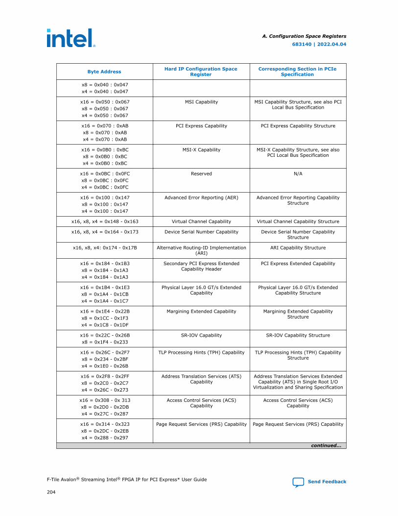
Byte Address Hard IP Configuration SpaceRegister
Corresponding Section in PCIeSpecification
x8 = 0x040 : 0x047x4 = 0x040 : 0x047
x16 = 0x050 : 0x067x8 = 0x050 : 0x067x4 = 0x050 : 0x067
MSI Capability MSI Capability Structure, see also PCILocal Bus Specification
x16 = 0x070 : 0xABx8 = 0x070 : 0xABx4 = 0x070 : 0xAB
PCI Express Capability PCI Express Capability Structure
x16 = 0x0B0 : 0xBCx8 = 0x0B0 : 0xBCx4 = 0x0B0 : 0xBC
MSI-X Capability MSI-X Capability Structure, see alsoPCI Local Bus Specification
x16 = 0x0BC : 0x0FCx8 = 0x0BC : 0x0FCx4 = 0x0BC : 0x0FC
Reserved N/A
x16 = 0x100 : 0x147x8 = 0x100 : 0x147x4 = 0x100 : 0x147
Advanced Error Reporting (AER) Advanced Error Reporting CapabilityStructure
x16, x8, x4 = 0x148 - 0x163 Virtual Channel Capability Virtual Channel Capability Structure
x16, x8, x4 = 0x164 - 0x173 Device Serial Number Capability Device Serial Number CapabilityStructure
x16, x8, x4: 0x174 - 0x17B Alternative Routing-ID Implementation(ARI)
ARI Capability Structure
x16 = 0x184 - 0x1B3x8 = 0x184 - 0x1A3x4 = 0x184 - 0x1A3
Secondary PCI Express ExtendedCapability Header
PCI Express Extended Capability
x16 = 0x1B4 - 0x1E3x8 = 0x1A4 - 0x1CBx4 = 0x1A4 - 0x1C7
Physical Layer 16.0 GT/s ExtendedCapability
Physical Layer 16.0 GT/s ExtendedCapability Structure
x16 = 0x1E4 - 0x22Bx8 = 0x1CC - 0x1F3x4 = 0x1C8 - 0x1DF
Margining Extended Capability Margining Extended CapabilityStructure
x16 = 0x22C - 0x26Bx8 = 0x1F4 - 0x233
SR-IOV Capability SR-IOV Capability Structure
x16 = 0x26C - 0x2F7x8 = 0x234 - 0x2BFx4 = 0x1E0 - 0x26B
TLP Processing Hints (TPH) Capability TLP Processing Hints (TPH) CapabilityStructure
x16 = 0x2F8 - 0x2FFx8 = 0x2C0 - 0x2C7x4 = 0x26C - 0x273
Address Translation Services (ATS)Capability
Address Translation Services ExtendedCapability (ATS) in Single Root I/O
Virtualization and Sharing Specification
x16 = 0x308 - 0x 313x8 = 0x2D0 - 0x2DBx4 = 0x27C - 0x287
Access Control Services (ACS)Capability
Access Control Services (ACS)Capability
x16 = 0x314 - 0x323x8 = 0x2DC - 0x2EBx4 = 0x288 - 0x297
Page Request Services (PRS) Capability Page Request Services (PRS) Capability
continued...
A. Configuration Space Registers
683140 | 2022.04.04
F-Tile Avalon® Streaming Intel® FPGA IP for PCI Express* User Guide Send Feedback
204
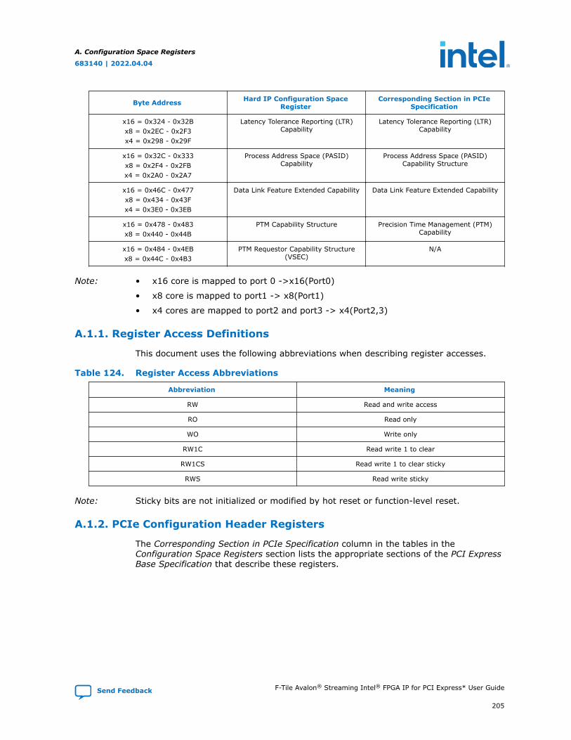
Byte Address Hard IP Configuration SpaceRegister
Corresponding Section in PCIeSpecification
x16 = 0x324 - 0x32Bx8 = 0x2EC - 0x2F3x4 = 0x298 - 0x29F
Latency Tolerance Reporting (LTR)Capability
Latency Tolerance Reporting (LTR)Capability
x16 = 0x32C - 0x333x8 = 0x2F4 - 0x2FBx4 = 0x2A0 - 0x2A7
Process Address Space (PASID)Capability
Process Address Space (PASID)Capability Structure
x16 = 0x46C - 0x477x8 = 0x434 - 0x43Fx4 = 0x3E0 - 0x3EB
Data Link Feature Extended Capability Data Link Feature Extended Capability
x16 = 0x478 - 0x483x8 = 0x440 - 0x44B
PTM Capability Structure Precision Time Management (PTM)Capability
x16 = 0x484 - 0x4EBx8 = 0x44C - 0x4B3
PTM Requestor Capability Structure(VSEC)
N/A
Note: • x16 core is mapped to port 0 ->x16(Port0)
• x8 core is mapped to port1 -> x8(Port1)
• x4 cores are mapped to port2 and port3 -> x4(Port2,3)
A.1.1. Register Access Definitions
This document uses the following abbreviations when describing register accesses.
Table 124. Register Access Abbreviations
Abbreviation Meaning
RW Read and write access
RO Read only
WO Write only
RW1C Read write 1 to clear
RW1CS Read write 1 to clear sticky
RWS Read write sticky
Note: Sticky bits are not initialized or modified by hot reset or function-level reset.
A.1.2. PCIe Configuration Header Registers
The Corresponding Section in PCIe Specification column in the tables in theConfiguration Space Registers section lists the appropriate sections of the PCI ExpressBase Specification that describe these registers.
A. Configuration Space Registers
683140 | 2022.04.04
Send Feedback F-Tile Avalon® Streaming Intel® FPGA IP for PCI Express* User Guide
205
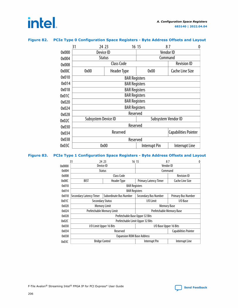
Figure 82. PCIe Type 0 Configuration Space Registers - Byte Address Offsets and Layout
0x0000x0040x0080x00C0x0100x0140x0180x01C0x0200x0240x0280x02C0x0300x0340x0380x03C
Device ID Vendor IDStatus Command
Class Code Revision ID
0x00 Header Type 0x00 Cache Line SizeBAR RegistersBAR RegistersBAR RegistersBAR RegistersBAR RegistersBAR Registers
ReservedSubsystem Device ID Subsystem Vendor ID
ReservedReserved
Reserved
Capabilities Pointer
0x00 Interrupt Pin Interrupt Line
31 24 23 16 15 8 7 0
Figure 83. PCIe Type 1 Configuration Space Registers - Byte Address Offsets and Layout
0x00000x004
Device ID31 24 23 16 15 8 7 0
0x0080x00C0x0100x0140x0180x01C0x0200x0240x0280x02C0x0300x0340x038
0x03C
Vendor ID
BIST Header Type Primary Latency Timer Cache Line Size
Status CommandClass Code Revision ID
BAR RegistersBAR Registers
Secondary Latency Timer Subordinate Bus Number Secondary Bus Number Primary Bus NumberSecondary Status I/O Limit I/O Base
Memory Limit Memory Base
Prefetchable Base Upper 32 BitsPrefetchable Limit Upper 32 Bits
I/O Limit Upper 16 Bits I/O Base Upper 16 BitsReserved Capabilities Pointer
Expansion ROM Base AddressBridge Control Interrupt Pin Interrupt Line
Prefetchable Memory Limit Prefetchable Memory Base
A. Configuration Space Registers
683140 | 2022.04.04
F-Tile Avalon® Streaming Intel® FPGA IP for PCI Express* User Guide Send Feedback
206
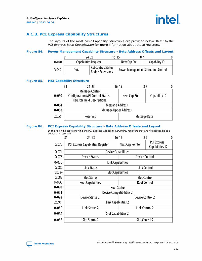
A.1.3. PCI Express Capability Structures
The layouts of the most basic Capability Structures are provided below. Refer to thePCI Express Base Specification for more information about these registers.
Figure 84. Power Management Capability Structure - Byte Address Offsets and Layout
0x040
0x04C
Capabilities Register Next Cap Ptr
Data
31 24 23 16 15 8 7 0Capability ID
Power Management Status and ControlPM Control/StatusBridge Extensions
Figure 85. MSI Capability Structure
0x050
0x0540x058
Message ControlConfiguration MSI Control Status
Register Field DescriptionsNext Cap Ptr
Message AddressMessage Upper Address
Reserved Message Data
31 24 23 16 15 8 7 0
0x05C
Capability ID
Figure 86. PCI Express Capability Structure - Byte Address Offsets and LayoutIn the following table showing the PCI Express Capability Structure, registers that are not applicable to adevice are reserved.
0x070
0x0740x0780x07C0x0800x0840x0880x08C0x0900x0940x0980x09C0x0A00x0A4
0x0A8
PCI Express Capabilities Register Next Cap Pointer
Device CapabilitiesDevice Status Device Control
Slot Capabilities
Root StatusDevice Compatibilities 2
Link Capabilities 2Link Status 2 Link Control 2
Slot Capabilities 2
Slot Status 2 Slot Control 2
31 24 23 16 15 8 7 0PCI Express
Capabilities ID
Link CapabilitiesLink Status Link Control
Slot Status Slot Control
Device Status 2 Device Control 2
Root Capabilities Root Control
A. Configuration Space Registers
683140 | 2022.04.04
Send Feedback F-Tile Avalon® Streaming Intel® FPGA IP for PCI Express* User Guide
207
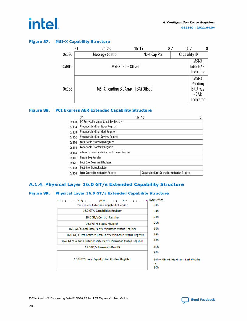
Figure 87. MSI-X Capability Structure
0x0B0
0x0B4
0x0B8
Message Control Next Cap Ptr
MSI-X Table Offset
MSI-X Pending Bit Array (PBA) Offset
31 24 23 16 15 8 7 0Capability ID
3 2
MSI-XTable BAR
IndicatorMSI-X
PendingBit Array
- BARIndicator
Figure 88. PCI Express AER Extended Capability Structure
0x100
0x104 Uncorrectable Error Status RegisterPCI Express Enhanced Capability Register
Uncorrectable Error Severity Register
Uncorrectable Error Mask Register0x108
0x10C
0x110
0x114
0x118
0x11C
0x12C
0x130
0x134
Correctable Error Status Register
Correctable Error Mask Register
Advanced Error Capabilities and Control Register
Header Log Register
Root Error Command Register
Root Error Status Register
Error Source Identification Register Correctable Error Source Identification Register
31 16 15 0
A.1.4. Physical Layer 16.0 GT/s Extended Capability Structure
Figure 89. Physical Layer 16.0 GT/s Extended Capability Structure
A. Configuration Space Registers
683140 | 2022.04.04
F-Tile Avalon® Streaming Intel® FPGA IP for PCI Express* User Guide Send Feedback
208
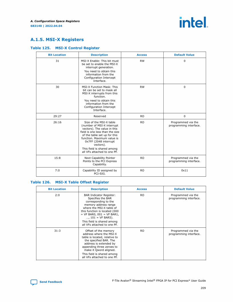
A.1.5. MSI-X Registers
Table 125. MSI-X Control Register
Bit Location Description Access Default Value
31 MSI-X Enable: This bit mustbe set to enable the MSI-X
interrupt generation.You need to obtain thisinformation from the
Configuration InterceptInterface.
RW 0
30 MSI-X Function Mask: Thisbit can be set to mask allMSI-X interrupts from this
function.You need to obtain thisinformation from the
Configuration InterceptInterface.
RW 0
29:27 Reserved RO 0
26:16 Size of the MSI-X table(number of MSI-X interruptvectors). The value in this
field is one less than the sizeof the table set up for thisfunction. Maximum value is
0x7FF (2048 interruptvectors).
This field is shared amongall VFs attached to one PF.
RO Programmed via theprogramming interface.
15:8 Next Capability PointerPoints to the PCI Express
Capability.
RO Programmed via theprogramming interface.
7:0 Capability ID assigned byPCI-SIG.
RO 0x11
Table 126. MSI-X Table Offset Register
Bit Location Description Access Default Value
2:0 BAR Indicator Register:Specifies the BAR
corresponding to thememory address range
where the MSI-X table ofthis function is located (000= VF BAR0, 001 = VF BAR1,
…, 101 = VF BAR5).This field is shared amongall VFs attached to one PF.
RO Programmed via theprogramming interface.
31:3 Offset of the memoryaddress where the MSI-X
table is located, relative tothe specified BAR. Theaddress is extended by
appending three zeroes tomake it Qword aligned.
This field is shared amongall VFs attached to one PF.
RO Programmed via theprogramming interface.
A. Configuration Space Registers
683140 | 2022.04.04
Send Feedback F-Tile Avalon® Streaming Intel® FPGA IP for PCI Express* User Guide
209
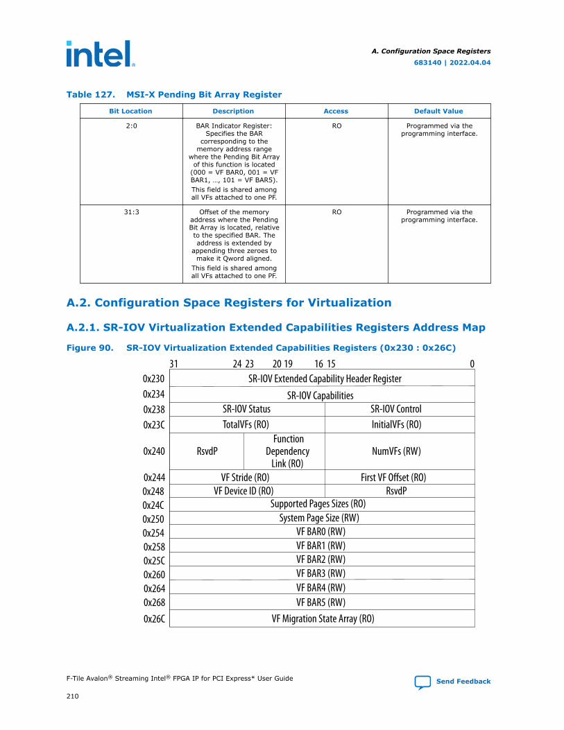
Table 127. MSI-X Pending Bit Array Register
Bit Location Description Access Default Value
2:0 BAR Indicator Register:Specifies the BAR
corresponding to thememory address range
where the Pending Bit Arrayof this function is located
(000 = VF BAR0, 001 = VFBAR1, …, 101 = VF BAR5).This field is shared amongall VFs attached to one PF.
RO Programmed via theprogramming interface.
31:3 Offset of the memoryaddress where the PendingBit Array is located, relativeto the specified BAR. Theaddress is extended by
appending three zeroes tomake it Qword aligned.
This field is shared amongall VFs attached to one PF.
RO Programmed via theprogramming interface.
A.2. Configuration Space Registers for Virtualization
A.2.1. SR-IOV Virtualization Extended Capabilities Registers Address Map
Figure 90. SR-IOV Virtualization Extended Capabilities Registers (0x230 : 0x26C)
0x2340x230
0x2380x23C
0x240
0x2440x2480x24C0x2500x2540x2580x25C0x2600x2640x2680x26C
31 24 23 16 1520 19 0
SR-IOV CapabilitiesSR-IOV Extended Capability Header Register
SR-IOV Status SR-IOV Control
Supported Pages Sizes (RO)System Page Size (RW)
VF BAR0 (RW)VF BAR1 (RW)
VF BAR5 (RW)VF Migration State Array (RO)
VF BAR4 (RW)VF BAR3 (RW)VF BAR2 (RW)
TotalVFs (RO) InitialVFs (RO)
RsvdP NumVFs (RW)
VF Stride (RO) First VF Offset (RO)VF Device ID (RO) RsvdP
FunctionDependency
Link (RO)
A. Configuration Space Registers
683140 | 2022.04.04
F-Tile Avalon® Streaming Intel® FPGA IP for PCI Express* User Guide Send Feedback
210
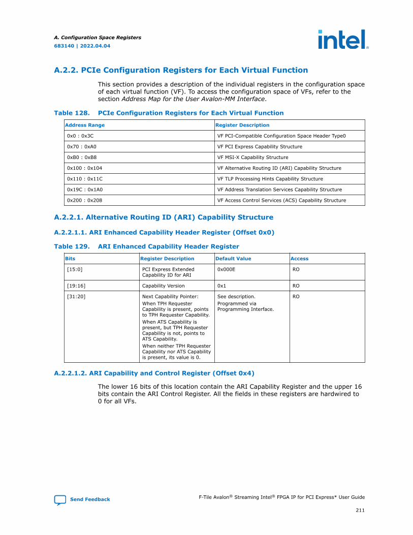
A.2.2. PCIe Configuration Registers for Each Virtual Function
This section provides a description of the individual registers in the configuration spaceof each virtual function (VF). To access the configuration space of VFs, refer to thesection Address Map for the User Avalon-MM Interface.
Table 128. PCIe Configuration Registers for Each Virtual Function
Address Range Register Description
0x0 : 0x3C VF PCI-Compatible Configuration Space Header Type0
0x70 : 0xA0 VF PCI Express Capability Structure
0xB0 : 0xB8 VF MSI-X Capability Structure
0x100 : 0x104 VF Alternative Routing ID (ARI) Capability Structure
0x110 : 0x11C VF TLP Processing Hints Capability Structure
0x19C : 0x1A0 VF Address Translation Services Capability Structure
0x200 : 0x208 VF Access Control Services (ACS) Capability Structure
A.2.2.1. Alternative Routing ID (ARI) Capability Structure
A.2.2.1.1. ARI Enhanced Capability Header Register (Offset 0x0)
Table 129. ARI Enhanced Capability Header Register
Bits Register Description Default Value Access
[15:0] PCI Express ExtendedCapability ID for ARI
0x000E RO
[19:16] Capability Version 0x1 RO
[31:20] Next Capability Pointer:When TPH RequesterCapability is present, pointsto TPH Requester Capability.When ATS Capability ispresent, but TPH RequesterCapability is not, points toATS Capability.When neither TPH RequesterCapability nor ATS Capabilityis present, its value is 0.
See description.Programmed viaProgramming Interface.
RO
A.2.2.1.2. ARI Capability and Control Register (Offset 0x4)
The lower 16 bits of this location contain the ARI Capability Register and the upper 16bits contain the ARI Control Register. All the fields in these registers are hardwired to0 for all VFs.
A. Configuration Space Registers
683140 | 2022.04.04
Send Feedback F-Tile Avalon® Streaming Intel® FPGA IP for PCI Express* User Guide
211
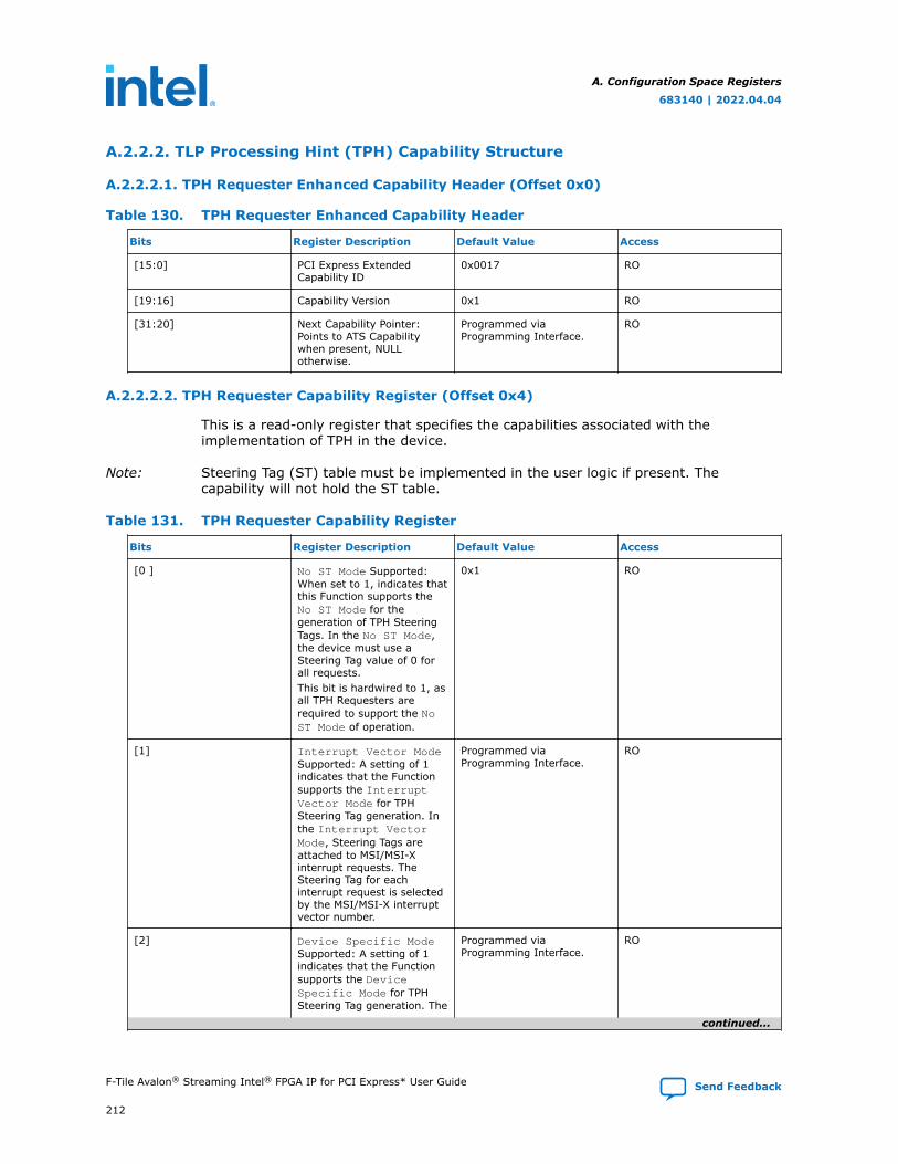
A.2.2.2. TLP Processing Hint (TPH) Capability Structure
A.2.2.2.1. TPH Requester Enhanced Capability Header (Offset 0x0)
Table 130. TPH Requester Enhanced Capability Header
Bits Register Description Default Value Access
[15:0] PCI Express ExtendedCapability ID
0x0017 RO
[19:16] Capability Version 0x1 RO
[31:20] Next Capability Pointer:Points to ATS Capabilitywhen present, NULLotherwise.
Programmed viaProgramming Interface.
RO
A.2.2.2.2. TPH Requester Capability Register (Offset 0x4)
This is a read-only register that specifies the capabilities associated with theimplementation of TPH in the device.
Note: Steering Tag (ST) table must be implemented in the user logic if present. Thecapability will not hold the ST table.
Table 131. TPH Requester Capability Register
Bits Register Description Default Value Access
[0 ] No ST Mode Supported:When set to 1, indicates thatthis Function supports theNo ST Mode for thegeneration of TPH SteeringTags. In the No ST Mode,the device must use aSteering Tag value of 0 forall requests.This bit is hardwired to 1, asall TPH Requesters arerequired to support the NoST Mode of operation.
0x1 RO
[1] Interrupt Vector ModeSupported: A setting of 1indicates that the Functionsupports the InterruptVector Mode for TPHSteering Tag generation. Inthe Interrupt VectorMode, Steering Tags areattached to MSI/MSI-Xinterrupt requests. TheSteering Tag for eachinterrupt request is selectedby the MSI/MSI-X interruptvector number.
Programmed viaProgramming Interface.
RO
[2] Device Specific ModeSupported: A setting of 1indicates that the Functionsupports the DeviceSpecific Mode for TPHSteering Tag generation. The
Programmed viaProgramming Interface.
RO
continued...
A. Configuration Space Registers
683140 | 2022.04.04
F-Tile Avalon® Streaming Intel® FPGA IP for PCI Express* User Guide Send Feedback
212
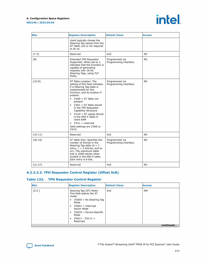
Bits Register Description Default Value Access
client typically choses theSteering Tag values from theST Table, but is not requiredto do so.
[7:3] Reserved 0x0 RO
[8] Extended TPH RequesterSupported: When set to 1,indicates that the Function iscapable of generatingrequests with 16-bitSteering Tags, using TLPPrefix.
Programmed viaProgramming Interface.
RO
[10:9] ST Table Location: Thesetting of this field indicatesif a Steering Tag table isimplemented for thisFunction, and its location ifpresent.• 2'b00 = ST Table not
present• 2'b01 = ST Table stored
in the TPH RequesterCapability Structure
• 2'b10 = ST values storedin the MSI-X Table inclient RAM
• 2'b11 = reservedValid settings are 2'b00 or2'b10.
Programmed viaProgramming Interface.
RO
[15:11] Reserved 0x0 RO
[26:16] ST Table Size: Specifies thenumber of entries in theSteering Tag table (0 = 1entry, 1 = 2 entries, and soon). The maximum tablesize is 2048 entries whenlocated in the MSI-X table.Each entry is 8 bits.
Programmed viaProgramming Interface.
RO
[31:27] Reserved 0x0 RO
A.2.2.2.3. TPH Requester Control Register (Offset 0x8)
Table 132. TPH Requester Control Register
Bits Register Description Default Value Access
[2:0 ] Steering Tag (ST) Mode:This field selects the STmode:• 3'b000 = No Steering Tag
Mode• 3'b001 = Interrupt
Vector Mode• 3'b010 = Device-Specific
Mode• 3'b011 - 3'b111 =
Reserved
0x0 RW
continued...
A. Configuration Space Registers
683140 | 2022.04.04
Send Feedback F-Tile Avalon® Streaming Intel® FPGA IP for PCI Express* User Guide
213
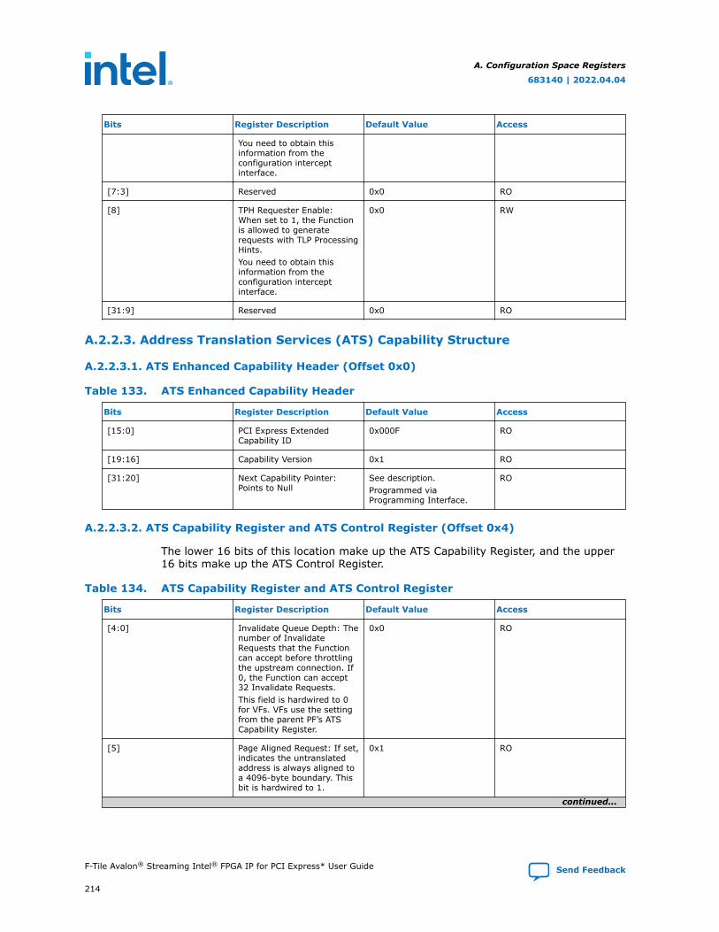
Bits Register Description Default Value Access
You need to obtain thisinformation from theconfiguration interceptinterface.
[7:3] Reserved 0x0 RO
[8] TPH Requester Enable:When set to 1, the Functionis allowed to generaterequests with TLP ProcessingHints.You need to obtain thisinformation from theconfiguration interceptinterface.
0x0 RW
[31:9] Reserved 0x0 RO
A.2.2.3. Address Translation Services (ATS) Capability Structure
A.2.2.3.1. ATS Enhanced Capability Header (Offset 0x0)
Table 133. ATS Enhanced Capability Header
Bits Register Description Default Value Access
[15:0] PCI Express ExtendedCapability ID
0x000F RO
[19:16] Capability Version 0x1 RO
[31:20] Next Capability Pointer:Points to Null
See description.Programmed viaProgramming Interface.
RO
A.2.2.3.2. ATS Capability Register and ATS Control Register (Offset 0x4)
The lower 16 bits of this location make up the ATS Capability Register, and the upper16 bits make up the ATS Control Register.
Table 134. ATS Capability Register and ATS Control Register
Bits Register Description Default Value Access
[4:0] Invalidate Queue Depth: Thenumber of InvalidateRequests that the Functioncan accept before throttlingthe upstream connection. If0, the Function can accept32 Invalidate Requests.This field is hardwired to 0for VFs. VFs use the settingfrom the parent PF’s ATSCapability Register.
0x0 RO
[5] Page Aligned Request: If set,indicates the untranslatedaddress is always aligned toa 4096-byte boundary. Thisbit is hardwired to 1.
0x1 RO
continued...
A. Configuration Space Registers
683140 | 2022.04.04
F-Tile Avalon® Streaming Intel® FPGA IP for PCI Express* User Guide Send Feedback
214
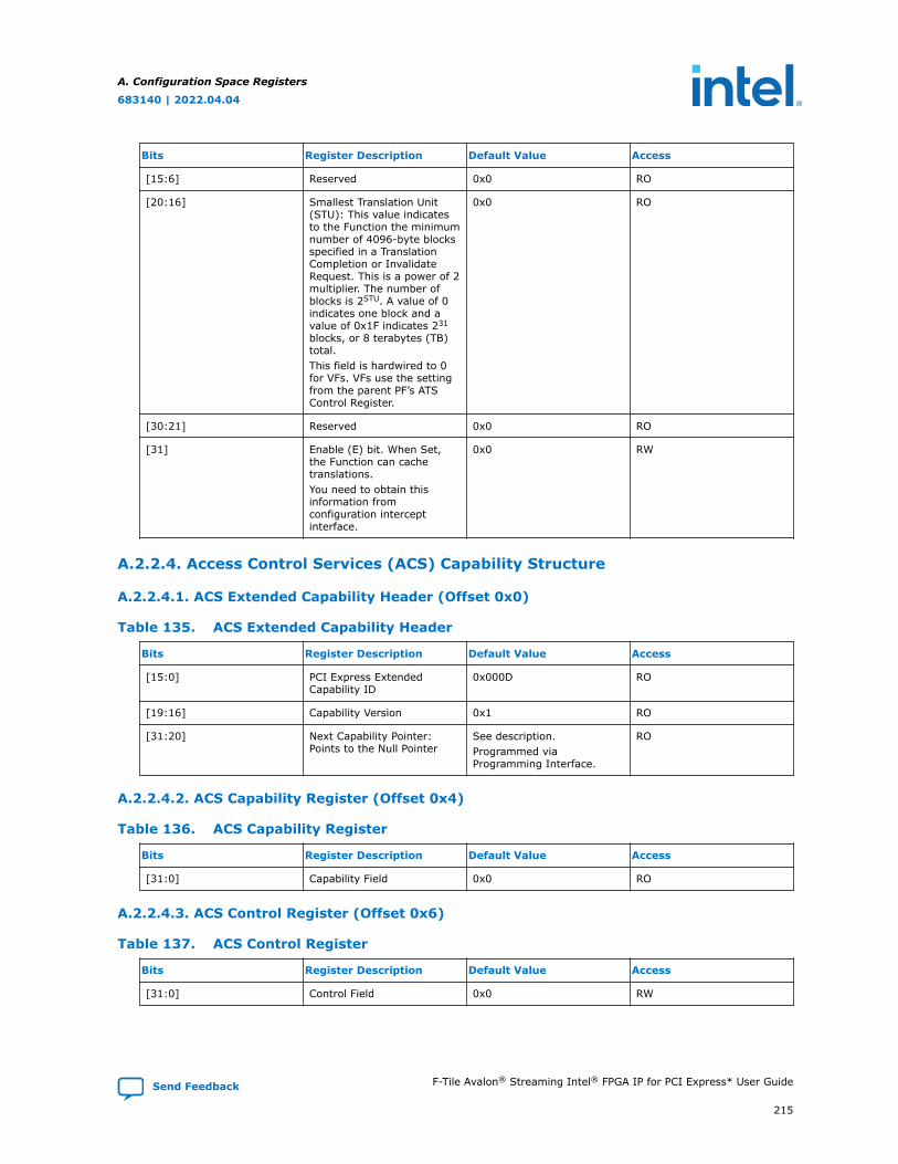
Bits Register Description Default Value Access
[15:6] Reserved 0x0 RO
[20:16] Smallest Translation Unit(STU): This value indicatesto the Function the minimumnumber of 4096-byte blocksspecified in a TranslationCompletion or InvalidateRequest. This is a power of 2multiplier. The number ofblocks is 2STU. A value of 0indicates one block and avalue of 0x1F indicates 231
blocks, or 8 terabytes (TB)total.This field is hardwired to 0for VFs. VFs use the settingfrom the parent PF’s ATSControl Register.
0x0 RO
[30:21] Reserved 0x0 RO
[31] Enable (E) bit. When Set,the Function can cachetranslations.You need to obtain thisinformation fromconfiguration interceptinterface.
0x0 RW
A.2.2.4. Access Control Services (ACS) Capability Structure
A.2.2.4.1. ACS Extended Capability Header (Offset 0x0)
Table 135. ACS Extended Capability Header
Bits Register Description Default Value Access
[15:0] PCI Express ExtendedCapability ID
0x000D RO
[19:16] Capability Version 0x1 RO
[31:20] Next Capability Pointer:Points to the Null Pointer
See description.Programmed viaProgramming Interface.
RO
A.2.2.4.2. ACS Capability Register (Offset 0x4)
Table 136. ACS Capability Register
Bits Register Description Default Value Access
[31:0] Capability Field 0x0 RO
A.2.2.4.3. ACS Control Register (Offset 0x6)
Table 137. ACS Control Register
Bits Register Description Default Value Access
[31:0] Control Field 0x0 RW
A. Configuration Space Registers
683140 | 2022.04.04
Send Feedback F-Tile Avalon® Streaming Intel® FPGA IP for PCI Express* User Guide
215
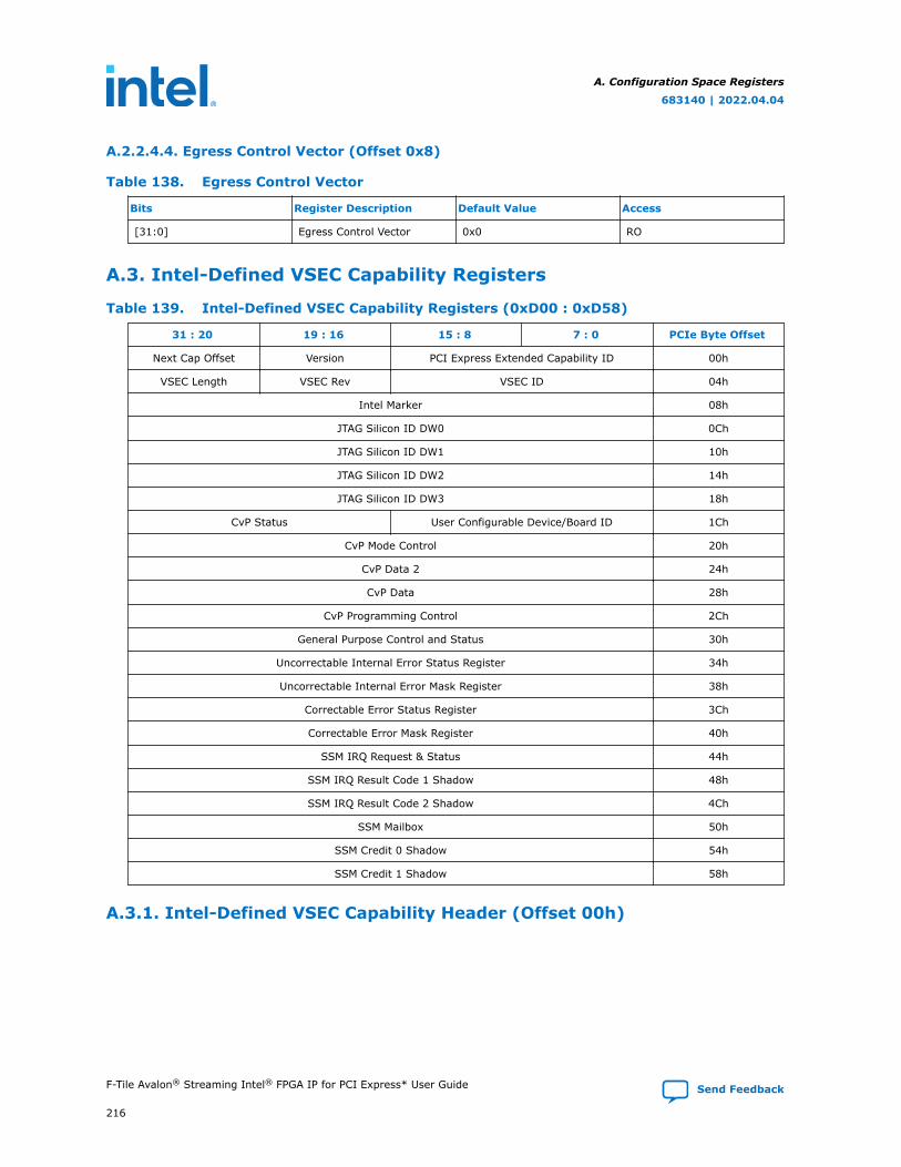
A.2.2.4.4. Egress Control Vector (Offset 0x8)
Table 138. Egress Control Vector
Bits Register Description Default Value Access
[31:0] Egress Control Vector 0x0 RO
A.3. Intel-Defined VSEC Capability Registers
Table 139. Intel-Defined VSEC Capability Registers (0xD00 : 0xD58)
31 : 20 19 : 16 15 : 8 7 : 0 PCIe Byte Offset
Next Cap Offset Version PCI Express Extended Capability ID 00h
VSEC Length VSEC Rev VSEC ID 04h
Intel Marker 08h
JTAG Silicon ID DW0 0Ch
JTAG Silicon ID DW1 10h
JTAG Silicon ID DW2 14h
JTAG Silicon ID DW3 18h
CvP Status User Configurable Device/Board ID 1Ch
CvP Mode Control 20h
CvP Data 2 24h
CvP Data 28h
CvP Programming Control 2Ch
General Purpose Control and Status 30h
Uncorrectable Internal Error Status Register 34h
Uncorrectable Internal Error Mask Register 38h
Correctable Error Status Register 3Ch
Correctable Error Mask Register 40h
SSM IRQ Request & Status 44h
SSM IRQ Result Code 1 Shadow 48h
SSM IRQ Result Code 2 Shadow 4Ch
SSM Mailbox 50h
SSM Credit 0 Shadow 54h
SSM Credit 1 Shadow 58h
A.3.1. Intel-Defined VSEC Capability Header (Offset 00h)
A. Configuration Space Registers
683140 | 2022.04.04
F-Tile Avalon® Streaming Intel® FPGA IP for PCI Express* User Guide Send Feedback
216
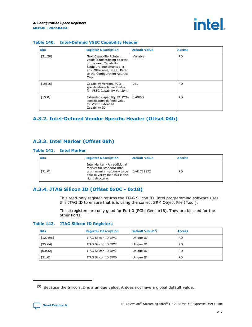
Table 140. Intel-Defined VSEC Capability Header
Bits Register Description Default Value Access
[31:20] Next Capability Pointer.Value is the starting addressof the next CapabilityStructure implemented, ifany. Otherwise, NULL. Referto the Configuration AddressMap.
Variable RO
[19:16] Capability Version. PCIespecification-defined valuefor VSEC Capability Version.
0x1 RO
[15:0] Extended Capability ID. PCIespecification-defined valuefor VSEC ExtendedCapability ID.
0x000B RO
A.3.2. Intel-Defined Vendor Specific Header (Offset 04h)
A.3.3. Intel Marker (Offset 08h)
Table 141. Intel Marker
Bits Register Description Default Value Access
[31:0]
Intel Marker - An additionalmarker for standard Intelprogramming software to beable to verify that this is theright structure.
0x41721172 RO
A.3.4. JTAG Silicon ID (Offset 0x0C - 0x18)
This read-only register returns the JTAG Silicon ID. Intel programming software usesthis JTAG ID to ensure that is is using the correct SRM Object File (*.sof).
These registers are only good for Port 0 (PCIe Gen4 x16). They are blocked for theother Ports.
Table 142. JTAG Silicon ID Registers
Bits Register Description Default Value(3) Access
[127:96] JTAG Silicon ID DW3 Unique ID RO
[95:64] JTAG Silicon ID DW2 Unique ID RO
[63:32] JTAG Silicon ID DW1 Unique ID RO
[31:0] JTAG Silicon ID DW0 Unique ID RO
(3) Because the Silicon ID is a unique value, it does not have a global default value.
A. Configuration Space Registers
683140 | 2022.04.04
Send Feedback F-Tile Avalon® Streaming Intel® FPGA IP for PCI Express* User Guide
217
A.3.5. User Configurable Device and Board ID (Offset 0x1C - 0x1D)
This register provides a user configurable device or board ID so that the user softwarecan determine which .sof file to load into the device.
This register is only available for Port 0 (PCIe Gen4 x16). It is blocked for the otherPorts.
Table 143. User Configurable Device and Board ID Register
Bits Register Description Default Value Access
[15:0] This register allows you tospecify the ID of the .soffile to be loaded.
From configuration bits RO
A.3.6. General Purpose Control and Status Register (Offset 0x30)
This register provides up to eight I/O pins each for Application Layer Control andStatus requirements. This feature supports Partial Reconfiguration of the FPGA fabric.Partial Reconfiguration only requires one input pin and one output pin. The otherseven I/Os make this interface extensible.
Table 144. General Purpose Control and Status Register
Bits Register Description Default Value Access
[31:16] Reserved. N/A RO
[15:8] General Purpose Status. TheApplication Layer can readthese status bits. These bitsare only available for Port 0(PCIe Gen4 x16). They areblocked for the other Ports.
0x00 RO
[7:0] General Purpose Control.The Application Layer canwrite these control bits.These bits are only availablefor Port 0 (PCIe Gen4 x16).They are blocked for theother Ports.
0x00 RW
A.3.7. Uncorrectable Internal Error Status Register (Offset 0x34)
This register reports the status of the internally checked errors that are uncorrectable.When these specific errors are enabled by the Uncorrectable Internal ErrorMask register, they are forwarded as Uncorrectable Internal Errors.
Note: This register is for debug only. Only use this register to observe behavior, not to drivelogic custom logic.
A. Configuration Space Registers
683140 | 2022.04.04
F-Tile Avalon® Streaming Intel® FPGA IP for PCI Express* User Guide Send Feedback
218
Table 145. Uncorrectable Internal Error Status Register
Bits Register Description Default Value Access
[31:13] Reserved 0x0 RO
[12] Debug Bus Interface (DBI)access error status fromConfig RAM block.
0x0 RW1CS
[11] Uncorrectable ECC errorfrom Config RAM block.
0x0 RW1C
[10:9] Reserved 0x0 RO
[8] RX Transaction Layer parityerror reported by the IPcore.
0x0 RW1CS
[7] TX Transaction Layer parityerror reported by the IPcore.
0x0 RW1CS
[6] Uncorrectable Internal Errorreported by the FPGA.
0x0 RW1CS
[5] cvp_config_error_latched: Configuration errordetected in CvP mode isreported as an uncorrectableerror. Set wheneverssm_cvp_config_error ofthe SSM Scratch CvP Statusregister bit[1] rises in CvPmode. This bit is onlyavailable for Port 0 (PCIeGen4 x16), but not for theother Ports.
0x0 RW1CS
[4:0] Reserved 0x0 RO
Note: The access code RW1CS represents Read Write 1 to Clear Sticky.
A.3.8. Uncorrectable Internal Error Mask Register (Offset 0x38)
This register controls which errors are forwarded as internal uncorrectable errors.
Table 146. Uncorrectable Internal Error Mask Register
Bits Register Description Default Value Access
[31:13] Reserved 0x0 RO
[12] Mask for Debug BusInterface (DBI) access error.
0x1 RWS
[11] Mask for Uncorrectable ECCerror from Config RAM block.
0x1 RWS
[10:9] Reserved 0x0 RO
[8] Mask for RX TransactionLayer parity error reportedby the IP core.
0x1 RWS
[7] Mask for TX TransactionLayer parity error reportedby the IP core.
0x1 RWS
continued...
A. Configuration Space Registers
683140 | 2022.04.04
Send Feedback F-Tile Avalon® Streaming Intel® FPGA IP for PCI Express* User Guide
219
Bits Register Description Default Value Access
[6] Mask for UncorrectableInternal error reported bythe FPGA.
0x1 RWS
[5] Mask for Configuration Errordetected in CvP mode. Thisbit is only available for Port0 (PCIe Gen4 x16), but notfor the other Ports.
0x0 RWS
[4:0] Reserved 0x0 RO
Note: The access code RWS stands for Read Write Sticky, meaning that the value is retainedafter a soft reset of the IP core.
A.3.9. Correctable Internal Error Status Register (Offset 0x3C)
The Correctable Internal Error Status register reports the status of theinternally checked errors that are correctable. When these specific errors are enabledby the Correctable Internal Error Mask register, they are forwarded ascorrectable internal errors. This register is for debug only. Only use this register toobserve behavior, not to drive custom logic
Table 147. Correctable Internal Error Status Register
Bits Register Description Default Value Access
[31:12] Reserved 0x0 RO
[11] Correctable ECC error statusfrom Config RAM.
0x0 RW1CS
[10:7] Reserved 0x0 RO
[6] Correctable Internal Errorreported by the FPGA.
0x0 RW1CS
[5] cvp_config_error_latched: Configuration errordetected in CvP mode (to bereported as correctable) -Set whenevercvp_config_error riseswhile in CvP mode. This bitis only available for Port 0(PCIe Gen4 x16), but not forthe other Ports.
0x0 RW1CS
[4:0] Reserved 0x0 RO
A.3.10. Correctable Internal Error Mask Register (Offset 0x40)
This register controls which errors are forwarded as internal correctable errors.
A. Configuration Space Registers
683140 | 2022.04.04
F-Tile Avalon® Streaming Intel® FPGA IP for PCI Express* User Guide Send Feedback
220
Table 148. Correctable Internal Error Mask Register
Bits Register Description Default Value Access
[31:12] Reserved 0x0 RO
[11] Mask for Correctable ECCerror status for Config RAM.
0x1 RWS
[10:7] Reserved 0x0 RWS
[6] Mask for CorrectableInternal Error reported bythe FPGA.
0x1 RWS
[5] Mask for Configuration Errordetected in CvP mode. Thisbit is only available for Port0 (PCIe Gen4 x16), but notfor the other Ports.
0x1 RWS
[4] Reserved 0x1 RWS
[3:0] Reserved 0x0 RWS
A. Configuration Space Registers
683140 | 2022.04.04
Send Feedback F-Tile Avalon® Streaming Intel® FPGA IP for PCI Express* User Guide
221
B. Implementation of Address Translation Services (ATS)in Endpoint Mode
With the F-Tile Avalon streaming IP for PCIe:
• ATS messages/completions are sent and received through the Avalon streaminginterface.
• Address translation caches (ATC) need to be implemented in the user logic. Theremust be a separate ATC for each VF/PF that supports ATS.
Refer to the Address Translation Services Revision 1.1 specification, section 4.1 PageRequest Message for more details.
B.1. Sending Translated/Untranslated Requests
The function with an ATC can send Memory Read requests that contain eithertranslated or untranslated addresses. If the Endpoint wants to receive the associatedtranslated address to update the ATC, it will generate a Memory Read with the"Translation Request" field set.
The Endpoint will receive the translated address in the associated Completion with theATS field's S/N/G/P/E/U/W/R values.
B.2. Sending a Page Request Message from the Endpoint (EP) to theRoot Complex (RC)
The user application issues a Page Request Message while using the Avalon-STinterface to send the contents of the ATS message.
The RC will respond with PRG Response message(s).
The EP will update its ATC accordingly.
B.3. Invalidating Requests/Completions
Invalidation is done via the Message mechanism:
• When the EP receives an Invalidate request from the RP, it needs to clear theassociated ATC.
• When the ATC is cleared, the user application generates a Completion message.
683140 | 2022.04.04
Send Feedback
Intel Corporation. All rights reserved. Intel, the Intel logo, and other Intel marks are trademarks of IntelCorporation or its subsidiaries. Intel warrants performance of its FPGA and semiconductor products to currentspecifications in accordance with Intel's standard warranty, but reserves the right to make changes to anyproducts and services at any time without notice. Intel assumes no responsibility or liability arising out of theapplication or use of any information, product, or service described herein except as expressly agreed to inwriting by Intel. Intel customers are advised to obtain the latest version of device specifications before relyingon any published information and before placing orders for products or services.*Other names and brands may be claimed as the property of others.
ISO9001:2015Registered
C. Packets Forwarded to the User Application in TLPBypass Mode
In TLP Bypass mode, the F-Tile IP for PCIe forwards TLPs to the Avalon-ST RXinterface except for malformed TLPs. The following tables describe how the IP handleseach TLP type for upstream and downstream.
C.1. EP TLP Bypass Mode (Upstream)
Table 149. Packets Forwarded in EP TLP Bypass Mode
TLP Type Routing Direction TLP Corruption Forwarded toAvalon-ST Interface
ASSERT/DEASSERTINTx Local Upstream
None No
Ecrc_err No
Malformed No
VENDOR_MESSAGE_0/1 Route_to_RC Upstream
NoneNo (VENDOR0)Yes (VENDOR1)
PoisonedNo (VENDOR0)Yes (VENDOR1)
Ecrc_err Yes
Malformed No
VENDOR_MESSAGE_0/1 Route_by_ID Both
None Yes
ID_mismatch Yes
Poisoned Yes
Ecrc_err Yes
Malformed No
VENDOR_MESSAGE_0/1 Broadcast Downstream
None Yes
Poisoned Yes
Ecrc_err Yes
Malformed No
VENDOR_MESSAGE_0/1 Local Both
None Yes
Poisoned Yes
Ecrc_err Yes
Malformed No
PM_ACTIVE_STATE_NAK Local Downstream None Yes
continued...
683140 | 2022.04.04
Send Feedback
Intel Corporation. All rights reserved. Intel, the Intel logo, and other Intel marks are trademarks of IntelCorporation or its subsidiaries. Intel warrants performance of its FPGA and semiconductor products to currentspecifications in accordance with Intel's standard warranty, but reserves the right to make changes to anyproducts and services at any time without notice. Intel assumes no responsibility or liability arising out of theapplication or use of any information, product, or service described herein except as expressly agreed to inwriting by Intel. Intel customers are advised to obtain the latest version of device specifications before relyingon any published information and before placing orders for products or services.*Other names and brands may be claimed as the property of others.
ISO9001:2015Registered

TLP Type Routing Direction TLP Corruption Forwarded toAvalon-ST Interface
Ecrc_err Yes
Malformed No
PM_PME Route_to_RC Upstream
None No
Ecrc_err Yes
Malformed No
PME_TURN_OFF Broadcast Downstream
None Yes
Ecrc_err Yes
Malformed No
PME_TO_ACK Gather Upstream
None No
Ecrc_err Yes
Malformed No
ERR_COR Route_to_RC Upstream
None No
Ecrc_err Yes
Malformed No
ERR_NONFATAL Route_to_RC Upstream
None No
Ecrc_err Yes
Malformed No
ERR_FATAL Route_to_RC Upstream
None No
Ecrc_err Yes
Malformed No
UNLOCK Broadcast Downstream
None Yes
Ecrc_err Yes
Malformed No
SET_SLOT_POWER_LIMIT Local Downstream
None Yes
Poisoned Yes
Ecrc_err Yes
Malformed No
LN_MESSAGE Route_by_ID Both
None Yes
ID_mismatch Yes
Poisoned Yes
Ecrc_err Yes
Malformed No
LN_MESSAGE Broadcast Downstream
None Yes
Poisoned Yes
Ecrc_err Yes
continued...
C. Packets Forwarded to the User Application in TLP Bypass Mode
683140 | 2022.04.04
F-Tile Avalon® Streaming Intel® FPGA IP for PCI Express* User Guide Send Feedback
224
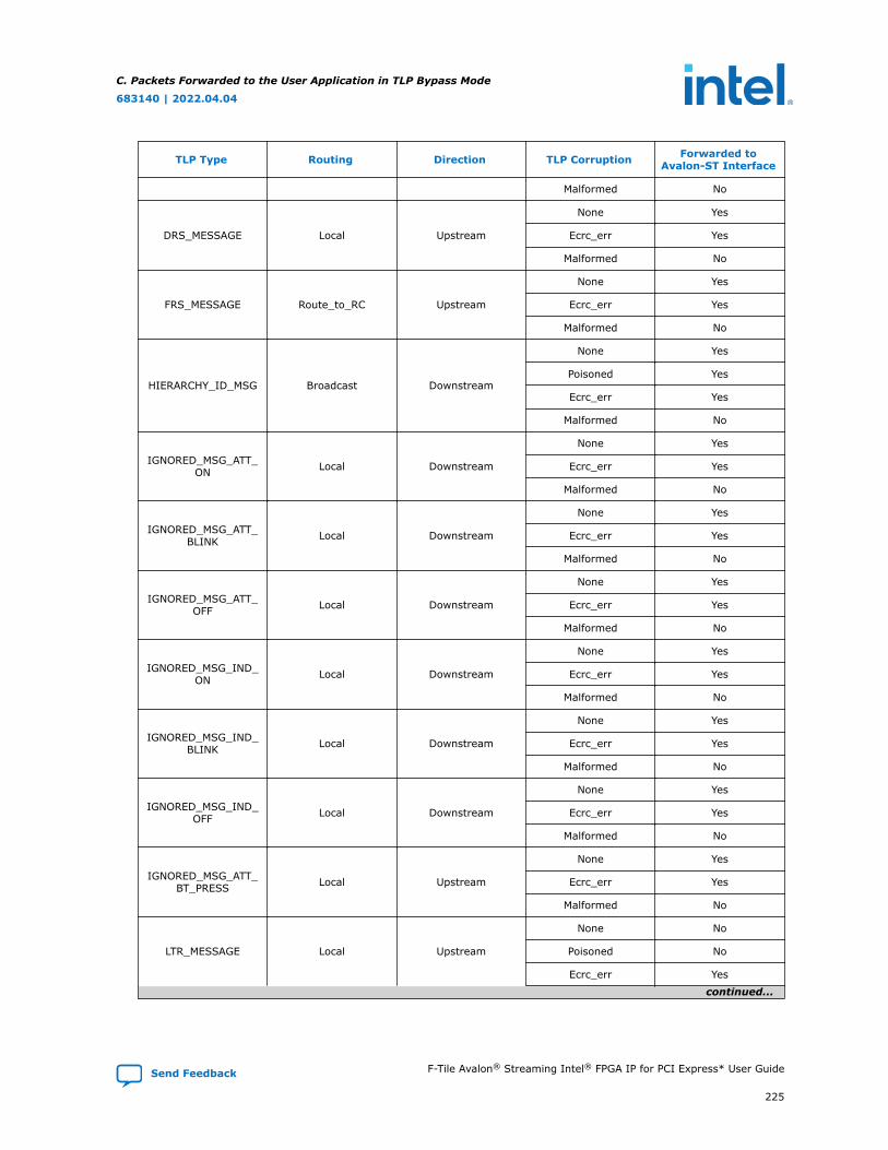
TLP Type Routing Direction TLP Corruption Forwarded toAvalon-ST Interface
Malformed No
DRS_MESSAGE Local Upstream
None Yes
Ecrc_err Yes
Malformed No
FRS_MESSAGE Route_to_RC Upstream
None Yes
Ecrc_err Yes
Malformed No
HIERARCHY_ID_MSG Broadcast Downstream
None Yes
Poisoned Yes
Ecrc_err Yes
Malformed No
IGNORED_MSG_ATT_ON Local Downstream
None Yes
Ecrc_err Yes
Malformed No
IGNORED_MSG_ATT_BLINK Local Downstream
None Yes
Ecrc_err Yes
Malformed No
IGNORED_MSG_ATT_OFF Local Downstream
None Yes
Ecrc_err Yes
Malformed No
IGNORED_MSG_IND_ON Local Downstream
None Yes
Ecrc_err Yes
Malformed No
IGNORED_MSG_IND_BLINK Local Downstream
None Yes
Ecrc_err Yes
Malformed No
IGNORED_MSG_IND_OFF Local Downstream
None Yes
Ecrc_err Yes
Malformed No
IGNORED_MSG_ATT_BT_PRESS Local Upstream
None Yes
Ecrc_err Yes
Malformed No
LTR_MESSAGE Local Upstream
None No
Poisoned No
Ecrc_err Yes
continued...
C. Packets Forwarded to the User Application in TLP Bypass Mode
683140 | 2022.04.04
Send Feedback F-Tile Avalon® Streaming Intel® FPGA IP for PCI Express* User Guide
225
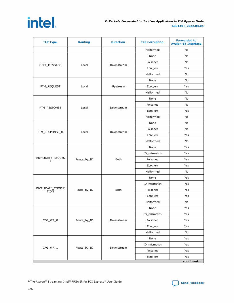
TLP Type Routing Direction TLP Corruption Forwarded toAvalon-ST Interface
Malformed No
OBFF_MESSAGE Local Downstream
None No
Poisoned No
Ecrc_err Yes
Malformed No
PTM_REQUEST Local Upstream
None No
Ecrc_err Yes
Malformed No
PTM_RESPONSE Local Downstream
None No
Poisoned No
Ecrc_err Yes
Malformed No
PTM_RESPONSE_D Local Downstream
None No
Poisoned No
Ecrc_err Yes
Malformed No
INVALIDATE_REQUEST Route_by_ID Both
None Yes
ID_mismatch Yes
Poisoned Yes
Ecrc_err Yes
Malformed No
INVALIDATE_COMPLETION Route_by_ID Both
None Yes
ID_mismatch Yes
Poisoned Yes
Ecrc_err Yes
Malformed No
CFG_WR_0 Route_by_ID Downstream
None Yes
ID_mismatch Yes
Poisoned Yes
Ecrc_err Yes
Malformed No
CFG_WR_1 Route_by_ID Downstream
None Yes
ID_mismatch Yes
Poisoned Yes
Ecrc_err Yes
continued...
C. Packets Forwarded to the User Application in TLP Bypass Mode
683140 | 2022.04.04
F-Tile Avalon® Streaming Intel® FPGA IP for PCI Express* User Guide Send Feedback
226
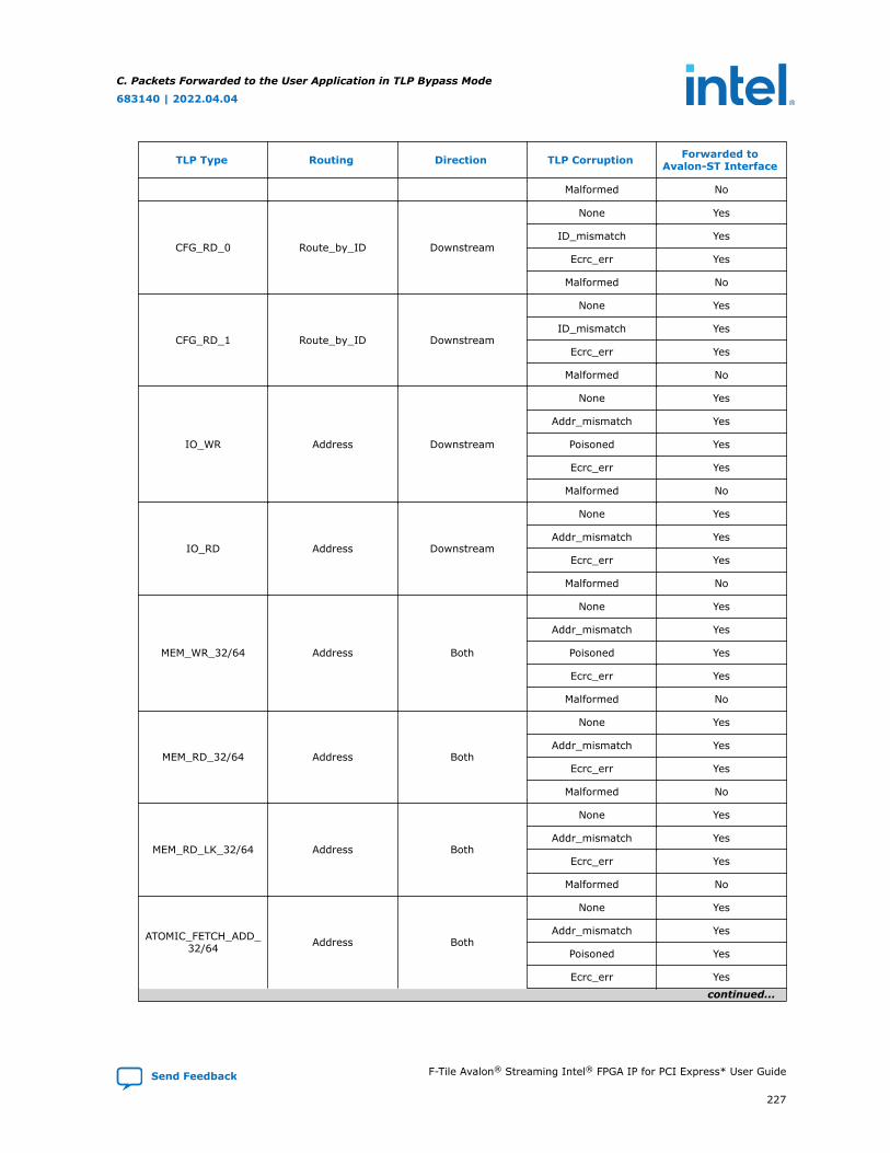
TLP Type Routing Direction TLP Corruption Forwarded toAvalon-ST Interface
Malformed No
CFG_RD_0 Route_by_ID Downstream
None Yes
ID_mismatch Yes
Ecrc_err Yes
Malformed No
CFG_RD_1 Route_by_ID Downstream
None Yes
ID_mismatch Yes
Ecrc_err Yes
Malformed No
IO_WR Address Downstream
None Yes
Addr_mismatch Yes
Poisoned Yes
Ecrc_err Yes
Malformed No
IO_RD Address Downstream
None Yes
Addr_mismatch Yes
Ecrc_err Yes
Malformed No
MEM_WR_32/64 Address Both
None Yes
Addr_mismatch Yes
Poisoned Yes
Ecrc_err Yes
Malformed No
MEM_RD_32/64 Address Both
None Yes
Addr_mismatch Yes
Ecrc_err Yes
Malformed No
MEM_RD_LK_32/64 Address Both
None Yes
Addr_mismatch Yes
Ecrc_err Yes
Malformed No
ATOMIC_FETCH_ADD_32/64 Address Both
None Yes
Addr_mismatch Yes
Poisoned Yes
Ecrc_err Yes
continued...
C. Packets Forwarded to the User Application in TLP Bypass Mode
683140 | 2022.04.04
Send Feedback F-Tile Avalon® Streaming Intel® FPGA IP for PCI Express* User Guide
227
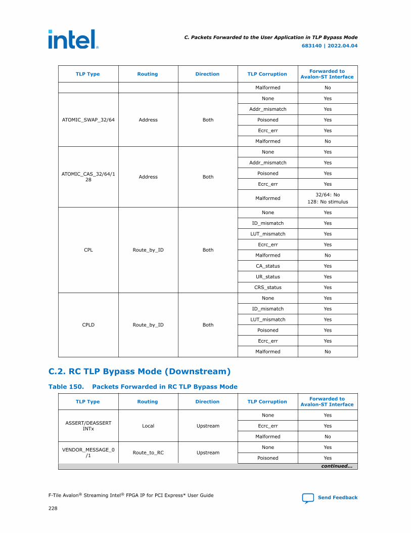
TLP Type Routing Direction TLP Corruption Forwarded toAvalon-ST Interface
Malformed No
ATOMIC_SWAP_32/64 Address Both
None Yes
Addr_mismatch Yes
Poisoned Yes
Ecrc_err Yes
Malformed No
ATOMIC_CAS_32/64/128 Address Both
None Yes
Addr_mismatch Yes
Poisoned Yes
Ecrc_err Yes
Malformed32/64: No
128: No stimulus
CPL Route_by_ID Both
None Yes
ID_mismatch Yes
LUT_mismatch Yes
Ecrc_err Yes
Malformed No
CA_status Yes
UR_status Yes
CRS_status Yes
CPLD Route_by_ID Both
None Yes
ID_mismatch Yes
LUT_mismatch Yes
Poisoned Yes
Ecrc_err Yes
Malformed No
C.2. RC TLP Bypass Mode (Downstream)
Table 150. Packets Forwarded in RC TLP Bypass Mode
TLP Type Routing Direction TLP Corruption Forwarded toAvalon-ST Interface
ASSERT/DEASSERTINTx Local Upstream
None Yes
Ecrc_err Yes
Malformed No
VENDOR_MESSAGE_0/1 Route_to_RC Upstream
None Yes
Poisoned Yes
continued...
C. Packets Forwarded to the User Application in TLP Bypass Mode
683140 | 2022.04.04
F-Tile Avalon® Streaming Intel® FPGA IP for PCI Express* User Guide Send Feedback
228
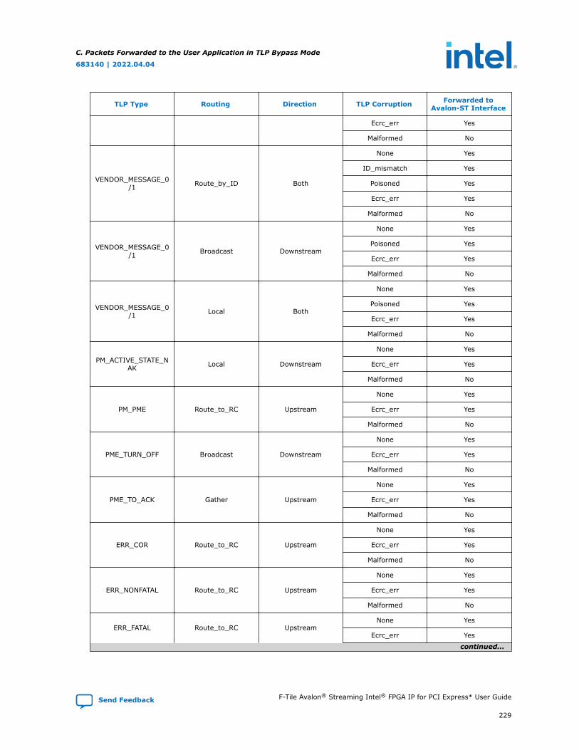
TLP Type Routing Direction TLP Corruption Forwarded toAvalon-ST Interface
Ecrc_err Yes
Malformed No
VENDOR_MESSAGE_0/1 Route_by_ID Both
None Yes
ID_mismatch Yes
Poisoned Yes
Ecrc_err Yes
Malformed No
VENDOR_MESSAGE_0/1 Broadcast Downstream
None Yes
Poisoned Yes
Ecrc_err Yes
Malformed No
VENDOR_MESSAGE_0/1 Local Both
None Yes
Poisoned Yes
Ecrc_err Yes
Malformed No
PM_ACTIVE_STATE_NAK Local Downstream
None Yes
Ecrc_err Yes
Malformed No
PM_PME Route_to_RC Upstream
None Yes
Ecrc_err Yes
Malformed No
PME_TURN_OFF Broadcast Downstream
None Yes
Ecrc_err Yes
Malformed No
PME_TO_ACK Gather Upstream
None Yes
Ecrc_err Yes
Malformed No
ERR_COR Route_to_RC Upstream
None Yes
Ecrc_err Yes
Malformed No
ERR_NONFATAL Route_to_RC Upstream
None Yes
Ecrc_err Yes
Malformed No
ERR_FATAL Route_to_RC UpstreamNone Yes
Ecrc_err Yes
continued...
C. Packets Forwarded to the User Application in TLP Bypass Mode
683140 | 2022.04.04
Send Feedback F-Tile Avalon® Streaming Intel® FPGA IP for PCI Express* User Guide
229

TLP Type Routing Direction TLP Corruption Forwarded toAvalon-ST Interface
Malformed No
UNLOCK Broadcast Downstream
None Yes
Ecrc_err Yes
Malformed No
SET_SLOT_POWER_LIMIT Local Downstream
None Yes
Poisoned Yes
Ecrc_err Yes
Malformed No
LN_MESSAGE Route_by_ID Both
None Yes
ID_mismatch Yes
Poisoned Yes
Ecrc_err Yes
Malformed No
LN_MESSAGE Broadcast Downstream
None Yes
Poisoned Yes
Ecrc_err Yes
Malformed No
DRS_MESSAGE Local Upstream
None Yes
Ecrc_err Yes
Malformed No
FRS_MESSAGE Route_to_RC Upstream
None Yes
Ecrc_err Yes
Malformed No
HIERARCHY_ID_MSG Broadcast Downstream
None Yes
Poisoned Yes
Ecrc_err Yes
Malformed No
IGNORED_MSG_ATT_ON Local Downstream
None Yes
Ecrc_err Yes
Malformed No
IGNORED_MSG_ATT_BLINK Local Downstream
None Yes
Ecrc_err Yes
Malformed No
IGNORED_MSG_ATT_OFF Local Downstream
None Yes
Ecrc_err Yes
continued...
C. Packets Forwarded to the User Application in TLP Bypass Mode
683140 | 2022.04.04
F-Tile Avalon® Streaming Intel® FPGA IP for PCI Express* User Guide Send Feedback
230
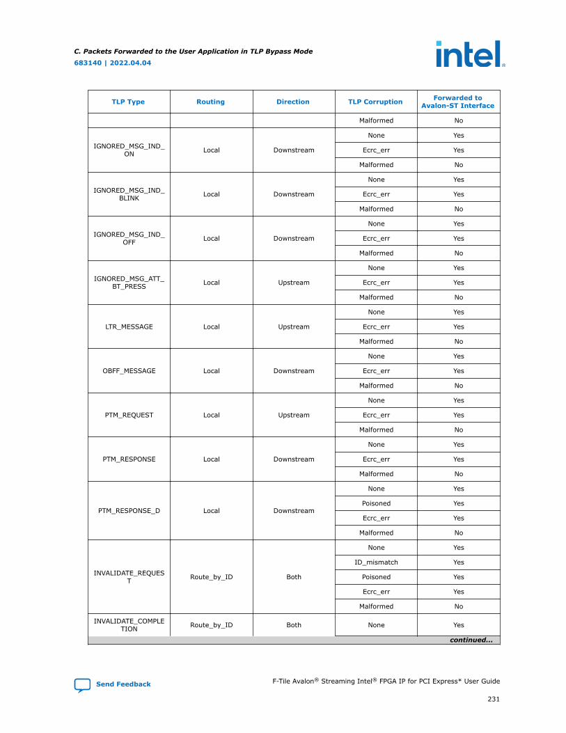
TLP Type Routing Direction TLP Corruption Forwarded toAvalon-ST Interface
Malformed No
IGNORED_MSG_IND_ON Local Downstream
None Yes
Ecrc_err Yes
Malformed No
IGNORED_MSG_IND_BLINK Local Downstream
None Yes
Ecrc_err Yes
Malformed No
IGNORED_MSG_IND_OFF Local Downstream
None Yes
Ecrc_err Yes
Malformed No
IGNORED_MSG_ATT_BT_PRESS Local Upstream
None Yes
Ecrc_err Yes
Malformed No
LTR_MESSAGE Local Upstream
None Yes
Ecrc_err Yes
Malformed No
OBFF_MESSAGE Local Downstream
None Yes
Ecrc_err Yes
Malformed No
PTM_REQUEST Local Upstream
None Yes
Ecrc_err Yes
Malformed No
PTM_RESPONSE Local Downstream
None Yes
Ecrc_err Yes
Malformed No
PTM_RESPONSE_D Local Downstream
None Yes
Poisoned Yes
Ecrc_err Yes
Malformed No
INVALIDATE_REQUEST Route_by_ID Both
None Yes
ID_mismatch Yes
Poisoned Yes
Ecrc_err Yes
Malformed No
INVALIDATE_COMPLETION Route_by_ID Both None Yes
continued...
C. Packets Forwarded to the User Application in TLP Bypass Mode
683140 | 2022.04.04
Send Feedback F-Tile Avalon® Streaming Intel® FPGA IP for PCI Express* User Guide
231
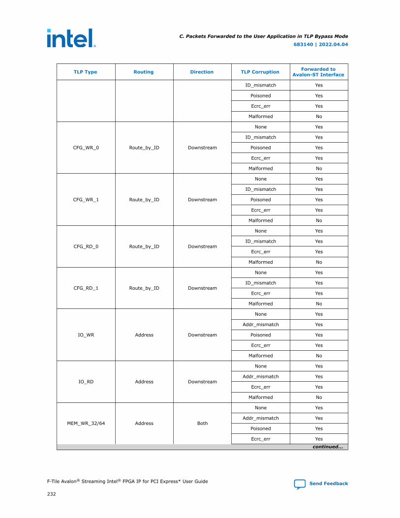
TLP Type Routing Direction TLP Corruption Forwarded toAvalon-ST Interface
ID_mismatch Yes
Poisoned Yes
Ecrc_err Yes
Malformed No
CFG_WR_0 Route_by_ID Downstream
None Yes
ID_mismatch Yes
Poisoned Yes
Ecrc_err Yes
Malformed No
CFG_WR_1 Route_by_ID Downstream
None Yes
ID_mismatch Yes
Poisoned Yes
Ecrc_err Yes
Malformed No
CFG_RD_0 Route_by_ID Downstream
None Yes
ID_mismatch Yes
Ecrc_err Yes
Malformed No
CFG_RD_1 Route_by_ID Downstream
None Yes
ID_mismatch Yes
Ecrc_err Yes
Malformed No
IO_WR Address Downstream
None Yes
Addr_mismatch Yes
Poisoned Yes
Ecrc_err Yes
Malformed No
IO_RD Address Downstream
None Yes
Addr_mismatch Yes
Ecrc_err Yes
Malformed No
MEM_WR_32/64 Address Both
None Yes
Addr_mismatch Yes
Poisoned Yes
Ecrc_err Yes
continued...
C. Packets Forwarded to the User Application in TLP Bypass Mode
683140 | 2022.04.04
F-Tile Avalon® Streaming Intel® FPGA IP for PCI Express* User Guide Send Feedback
232
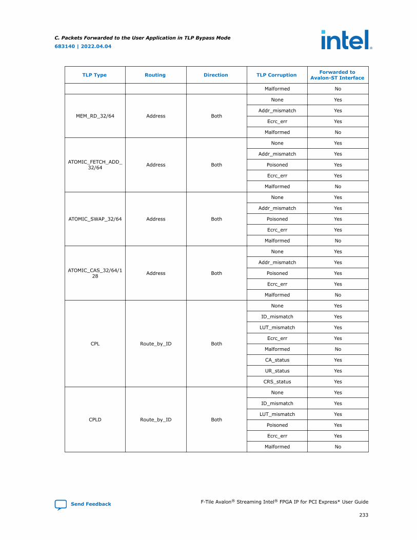
TLP Type Routing Direction TLP Corruption Forwarded toAvalon-ST Interface
Malformed No
MEM_RD_32/64 Address Both
None Yes
Addr_mismatch Yes
Ecrc_err Yes
Malformed No
ATOMIC_FETCH_ADD_32/64 Address Both
None Yes
Addr_mismatch Yes
Poisoned Yes
Ecrc_err Yes
Malformed No
ATOMIC_SWAP_32/64 Address Both
None Yes
Addr_mismatch Yes
Poisoned Yes
Ecrc_err Yes
Malformed No
ATOMIC_CAS_32/64/128 Address Both
None Yes
Addr_mismatch Yes
Poisoned Yes
Ecrc_err Yes
Malformed No
CPL Route_by_ID Both
None Yes
ID_mismatch Yes
LUT_mismatch Yes
Ecrc_err Yes
Malformed No
CA_status Yes
UR_status Yes
CRS_status Yes
CPLD Route_by_ID Both
None Yes
ID_mismatch Yes
LUT_mismatch Yes
Poisoned Yes
Ecrc_err Yes
Malformed No
C. Packets Forwarded to the User Application in TLP Bypass Mode
683140 | 2022.04.04
Send Feedback F-Tile Avalon® Streaming Intel® FPGA IP for PCI Express* User Guide
233
D. Root Port EnumerationThis chapter provides a flow chart that explains the Root Port enumeration process.The goal of enumeration is to find all connected devices in the system and for eachconnected device, set the necessary registers and make address range assignments.
At the end of the enumeration process, the Root Port (RP) must set the followingregisters:
• Primary Bus, Secondary Bus and Subordinate Bus numbers
• Memory Base and Limit
• I/O Base and I/O Limit
• Maximum Payload Size
• Memory Space Enable bit
The Endpoint (EP) must also have the following registers set by the RP:
• Master Enable bit
• BAR Address
• Maximum Payload Size
• Memory Space Enable bit
• Severity bit
The figure below shows an example tree of connected devices on which the followingflow chart will be based.
683140 | 2022.04.04
Send Feedback
Intel Corporation. All rights reserved. Intel, the Intel logo, and other Intel marks are trademarks of IntelCorporation or its subsidiaries. Intel warrants performance of its FPGA and semiconductor products to currentspecifications in accordance with Intel's standard warranty, but reserves the right to make changes to anyproducts and services at any time without notice. Intel assumes no responsibility or liability arising out of theapplication or use of any information, product, or service described herein except as expressly agreed to inwriting by Intel. Intel customers are advised to obtain the latest version of device specifications before relyingon any published information and before placing orders for products or services.*Other names and brands may be claimed as the property of others.
ISO9001:2015Registered
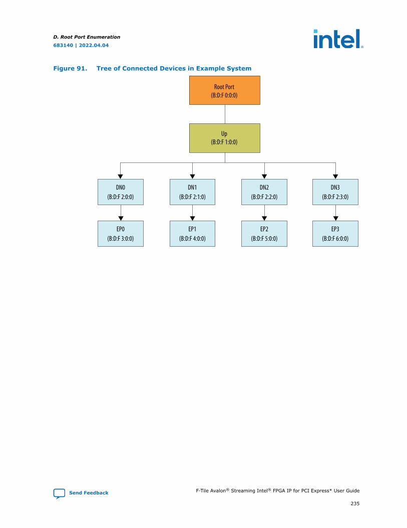
Figure 91. Tree of Connected Devices in Example System
Root Port(B:D:F 0:0:0)
DN0(B:D:F 2:0:0)
EP0(B:D:F 3:0:0)
DN1(B:D:F 2:1:0)
EP1(B:D:F 4:0:0)
DN2(B:D:F 2:2:0)
EP2(B:D:F 5:0:0)
DN3(B:D:F 2:3:0)
EP3(B:D:F 6:0:0)
Up(B:D:F 1:0:0)
D. Root Port Enumeration
683140 | 2022.04.04
Send Feedback F-Tile Avalon® Streaming Intel® FPGA IP for PCI Express* User Guide
235
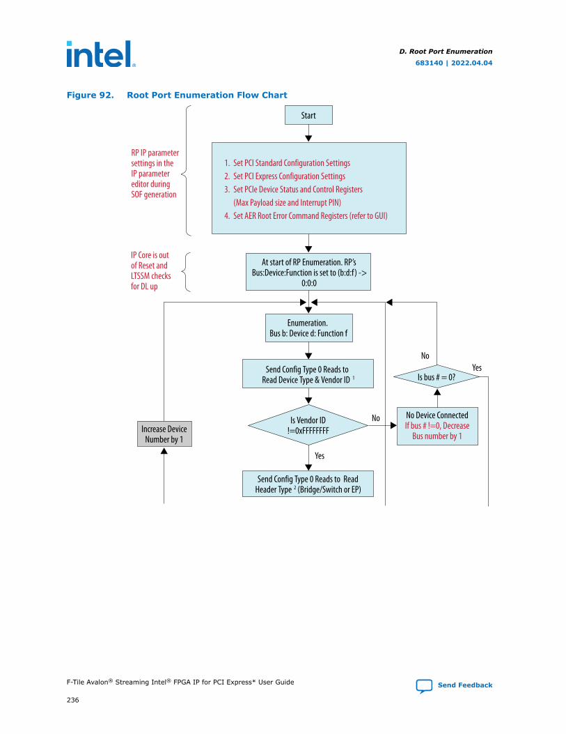
Figure 92. Root Port Enumeration Flow Chart
At start of RP Enumeration. RP’sBus:Device:Function is set to (b:d:f) ->
0:0:0
IP Core is outof Reset andLTSSM checksfor DL up
RP IP parametersettings in theIP parametereditor duringSOF generation
Send Config Type 0 Reads to ReadHeader Type 2 (Bridge/Switch or EP)
Yes
Yes
No
No
Increase DeviceNumber by 1
No Device ConnectedIf bus # !=0, Decrease
Bus number by 1
Send Config Type 0 Reads to Read Device Type & Vendor ID 1
Enumeration. Bus b: Device d: Function f
Is bus # = 0?
Is Vendor ID!=0xFFFFFFFF
Start
1. Set PCI Standard Configuration Settings2. Set PCI Express Configuration Settings3. Set PCIe Device Status and Control Registers (Max Payload size and Interrupt PIN)4. Set AER Root Error Command Registers (refer to GUI)
D. Root Port Enumeration
683140 | 2022.04.04
F-Tile Avalon® Streaming Intel® FPGA IP for PCI Express* User Guide Send Feedback
236
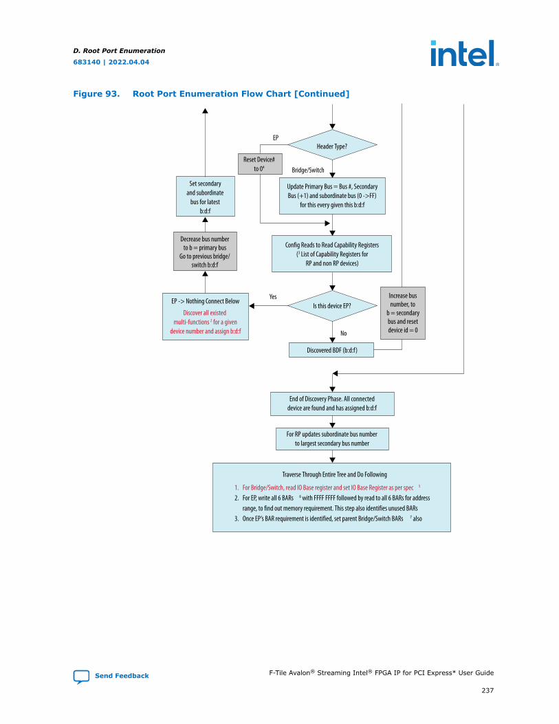
Figure 93. Root Port Enumeration Flow Chart [Continued]
1. For Bridge/Switch, read IO Base register and set IO Base Register as per spec 5
2. For EP, write all 6 BARs 6 with FFFF FFFF followed by read to all 6 BARs for address range, to find out memory requirement. This step also identifies unused BARs3. Once EP’s BAR requirement is identified, set parent Bridge/Switch BARs 7 also
Traverse Through Entire Tree and Do Following
Config Reads to Read Capability Registers(3 List of Capability Registers for
RP and non RP devices)
EP -> Nothing Connect Below
Discover all existed multi-functions 2 for a given
device number and assign b:d:f
Set secondaryand subordinate
bus for latestb:d:f
Update Primary Bus = Bus #, SecondaryBus (+1) and subordinate bus (0 ->FF)
for this every given this b:d:f
Header Type?
Bridge/Switch
EP
Discovered BDF (b:d:f)
Yes
No
Reset Device#to 04
Decrease bus numberto b = primary bus
Go to previous bridge/switch b:d:f
End of Discovery Phase. All connecteddevice are found and has assigned b:d:f
For RP updates subordinate bus numberto largest secondary bus number
Increase busnumber, to
b = secondarybus and resetdevice id = 0
Is this device EP?
D. Root Port Enumeration
683140 | 2022.04.04
Send Feedback F-Tile Avalon® Streaming Intel® FPGA IP for PCI Express* User Guide
237
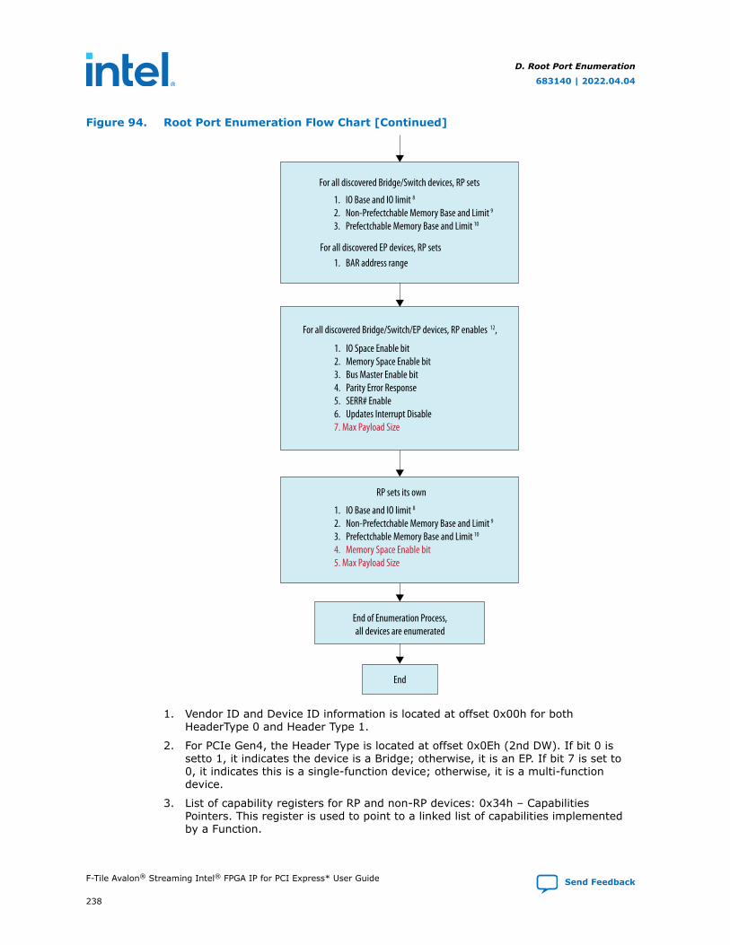
Figure 94. Root Port Enumeration Flow Chart [Continued]
End
1. IO Base and IO limit 8
2. Non-Prefectchable Memory Base and Limit 9
3. Prefectchable Memory Base and Limit 10
1. BAR address range
For all discovered Bridge/Switch devices, RP sets
For all discovered EP devices, RP sets
For all discovered Bridge/Switch/EP devices, RP enables 12,
1. IO Space Enable bit2. Memory Space Enable bit3. Bus Master Enable bit4. Parity Error Response5. SERR# Enable6. Updates Interrupt Disable7. Max Payload Size
1. IO Base and IO limit 8
2. Non-Prefectchable Memory Base and Limit 9
3. Prefectchable Memory Base and Limit 10
4. Memory Space Enable bit5. Max Payload Size
End of Enumeration Process,all devices are enumerated
RP sets its own
1. Vendor ID and Device ID information is located at offset 0x00h for bothHeaderType 0 and Header Type 1.
2. For PCIe Gen4, the Header Type is located at offset 0x0Eh (2nd DW). If bit 0 issetto 1, it indicates the device is a Bridge; otherwise, it is an EP. If bit 7 is set to0, it indicates this is a single-function device; otherwise, it is a multi-functiondevice.
3. List of capability registers for RP and non-RP devices: 0x34h – CapabilitiesPointers. This register is used to point to a linked list of capabilities implementedby a Function.
D. Root Port Enumeration
683140 | 2022.04.04
F-Tile Avalon® Streaming Intel® FPGA IP for PCI Express* User Guide Send Feedback
238
• Capabilities Pointer for RP:
— Address 60 - Identifies the Power Management Capability ID
— Address 6c - Identifies MSI Capability ID
— Address b4 - Identifies the PCI Express Capability structure
• Capabilities Pointer for non-RP:
— Address 40 - Identifies Power Management Capability ID
— Address 48 - Identifies the PCI Express Capability structure
4. EP does not have an associated register of Primary, Secondary andSubordinateBus numbers.
5. Bridge/Switch IO Base and Limit register offset 0x1Ch. These registers are setperthe PCIe 4.0 Base Specification. For more accurate information and flow, referto chapter 7.5.1.3.6 of the Base Specification.
6. For EP Type 0 header, BAR addresses are located at the following offsets:
• 0x10h – Base Address 0
• 0x14h – Base Address 1
• 0x18h – Base Address 2
• 0x1ch – Base Address 3
• 0x20h – Base Address 4
• 0x24h – Base Address 5
7. For Bridge/Switch Type 1 header, BAR addresses are located at the followingoffsets:
• 0x10h – Base Address 0
• 0x14h – Base Address 1
8. For Bridge/Switch Type 1 header, IO Base and IO limit registers are located atoffset 0x1Ch.
9. For Bridge/Switch Type 1 header, Non-Prefetchable Memory Base andLimitregisters are located at offset 0x20h.
10. For Bridge/Switch Type 1 header, Prefetchable Memory Base and Limit registersarelocated at offset 0x24h.
11. For Bridge/Switch/EP Type 0 & 1 headers, the Bus Master Enable bit is located atoffset 0x04h (Command Register) bit 2.
12. For Bridge/Switch/EP Type 0 & 1 headers:
• I/O Space Enable bit is located at offset 0x04h (Command Register) bit 0.
• Memory Space Enable bit is located at offset 0x04h (Command Register) bit 1.
• Bus Master Enable bit is located at offset 0x04h (Command Register) bit 2.
• Parity Error Response bit is located at offset 0x04h (Command Register) bit 6.
• SERR# Enable bit is located at offset 0x04h (Command Register) bit 8.
• Interrupt Disable bit is located at offset 0x04h (Command Register) bit 10.
D. Root Port Enumeration
683140 | 2022.04.04
Send Feedback F-Tile Avalon® Streaming Intel® FPGA IP for PCI Express* User Guide
239
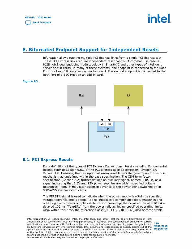
E. Bifurcated Endpoint Support for Independent ResetsBifurcation allows running multiple PCI Express links from a single PCI Express slot.These PCI Express links require independent reset control. A common use case isPCIE_x8x8 dual endpoint mode topology in SmartNIC and other types of intelligentserver add-in cards. In many of these systems, one endpoint is connected to the RootPort of a Host CPU on a server motherboard. The second endpoint is connected to theRoot Port of a SoC Host on an add-in card.
Figure 95.
Host SoC
FPGA
F-Tilex8 x8
E.1. PCI Express Resets
For a definition of the types of PCI Express Conventional Reset (including FundamentalReset), refer to Section 6.6.1 of the PCI Express Base Specification Revision 5.0Version 1.0. However, the description of warm reset leaves the generation of this resetmechanism as undefined within the base specification. The CEM form factorspecification (Section 2.2) further defines an auxiliary signal, named PERST#, as asignal indicating that 3.3V and 12V power supplies are within specified voltagetolerances. PERST# may later assert in advance of the power being switched off inS3/S4/S5 system sleep states.
The PERST# signal is used to indicate when the power supply is within its specifiedvoltage tolerance and is stable. It also initializes a component’s state machines andother logic once power supplies stabilize. On power-up, the de-assertion of PERST# isdelayed 100 ms (TpvpERL) from the power rails achieving specified operating limits.Also, within this time, the reference clocks (REFCLK+, REFCLK-) also become stable,
683140 | 2022.04.04
Send Feedback
Intel Corporation. All rights reserved. Intel, the Intel logo, and other Intel marks are trademarks of IntelCorporation or its subsidiaries. Intel warrants performance of its FPGA and semiconductor products to currentspecifications in accordance with Intel's standard warranty, but reserves the right to make changes to anyproducts and services at any time without notice. Intel assumes no responsibility or liability arising out of theapplication or use of any information, product, or service described herein except as expressly agreed to inwriting by Intel. Intel customers are advised to obtain the latest version of device specifications before relyingon any published information and before placing orders for products or services.*Other names and brands may be claimed as the property of others.
ISO9001:2015Registered
at least TPERST-CLK before PERST# is de-asserted. PERST# is asserted in advance ofthe power being switched off in a power-managed state like S3. PERST# is assertedwhen the power supply is powered down, but without the advanced warning of thetransition.
The CEM specification describes PERST# as a power-stable indicator indicative of acold-reset. Once again, PERST# is intended to be a globally distributed signal to allsystem components and adapters and can be used to reset a component to its initialconditions.
In a typical system, the in-band conventional reset mechanism (Hot Reset) can beused to return a specific component or tier of downstream components behind a givenRoot Port back to initial conditions, under a software-controlled mechanism(Secondary Bus reset bit). This mechanism can be used to reset portions of the PCIehierarchy, and requires that PERST# is not cycled, and power not removed from agiven component. This Hot Reset mechanism is the preferred mechanism to issueindependent conventional reset to different F-Tile endpoints residing in the samecomponent and/or adapter.
This Appendix describes how you can use a bifurcated two-endpoint configuration of F-Tile connected to independent systems/hosts.
Related Information
• PCI Express Base Specification Revision 5.0 Version 1.0
• PCI Express Card Electromechanical Specification
• Advanced Configuration and Power Interface (ACPI) Specification Version 6.4
E.2. Supported Configurations
E.2.1. Configuration Type A
Port 0, Port 1 and System Clock obtain free running clock. When PERST# is assertedfrom Host0 or Host1, the reference clock is not removed.
You have the option to:
• Shared Port0 RefClk, Port1 RefClk or SysPLL RefClk to the same reference clockpin depending on user selection
• Map Port0 RefClk, Port1 RefClk or SysPLL RefClk to individual reference clock pinwhere the free running clock is provided from the Host card.
Variations of free running clock source is illustrated in the diagrams below.
E. Bifurcated Endpoint Support for Independent Resets
683140 | 2022.04.04
Send Feedback F-Tile Avalon® Streaming Intel® FPGA IP for PCI Express* User Guide
241
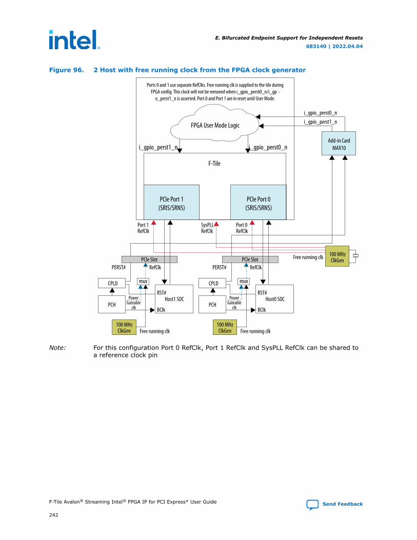
Figure 96. 2 Host with free running clock from the FPGA clock generator
i_gpio_perst1_n i_gpio_perst0_n
i_gpio_perst0_ni_gpio_perst1_n
Port 0RefClk
Port 1RefClk
PowerGateable
clk
RefClkPERST#
SysPLLRefClk
PCle Port 0(SRIS/SRNS)
Free running clk
PowerGateable
clk
RefClkPERST#
Free running clk
Free running clk
FPGA User Mode Logic
Ports 0 and 1 use separate RefClks. Free running clk is supplied to the tile during FPGA config. This clock will not be removed when i_gpio_perst0_n/i_gp -
o_perst1_n is asserted. Port 0 and Port 1 are in reset until User Mode.
PCle Port 1(SRIS/SRNS)
100 MHzClkGen
100 MHzClkGen
100 MHzClkGen
PCle SlotPCle Slot
mux
RST#
BClk
CPLD
Host1 SOCPCH
mux
RST#
BClk
CPLD
Host0 SOCPCH
F-Tile
Add-in CardMAX10
Note: For this configuration Port 0 RefClk, Port 1 RefClk and SysPLL RefClk can be shared toa reference clock pin
E. Bifurcated Endpoint Support for Independent Resets
683140 | 2022.04.04
F-Tile Avalon® Streaming Intel® FPGA IP for PCI Express* User Guide Send Feedback
242
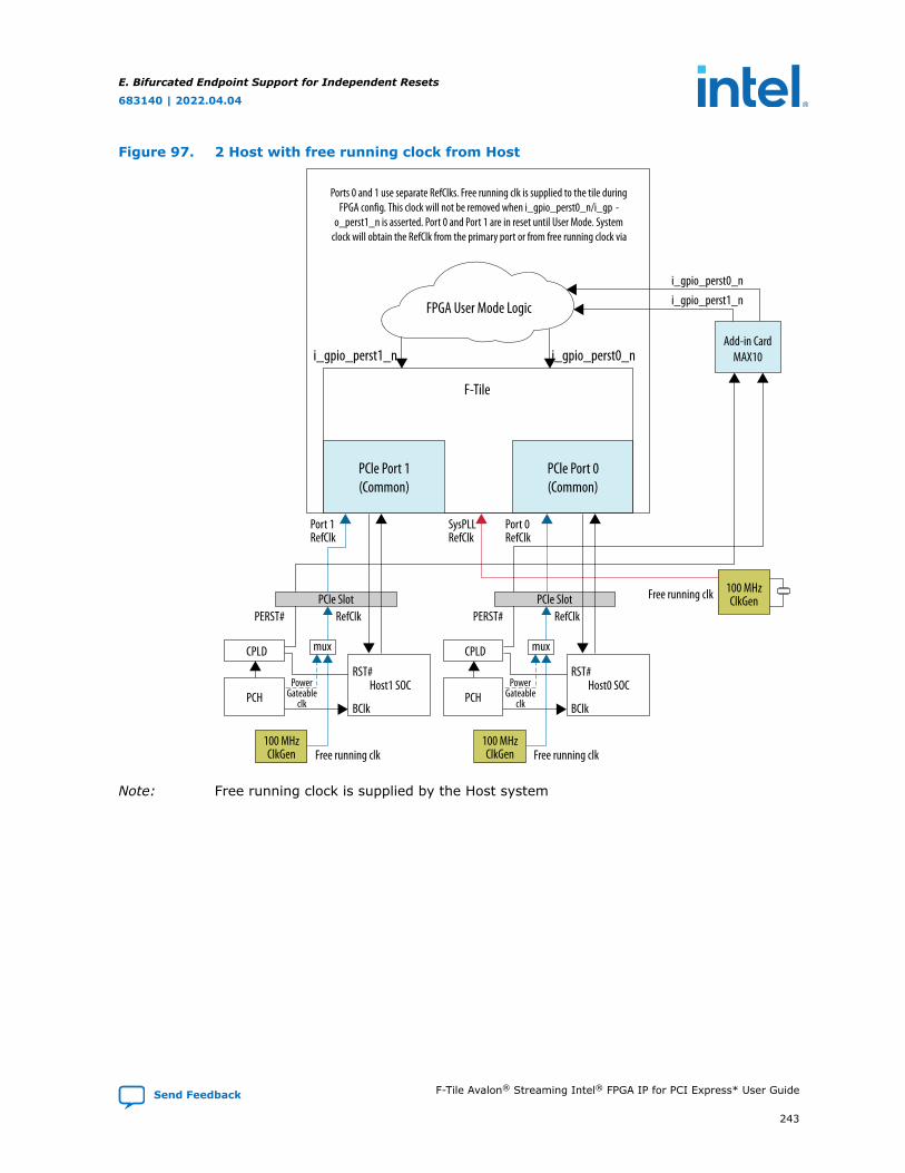
Figure 97. 2 Host with free running clock from Host
i_gpio_perst1_n i_gpio_perst0_n
i_gpio_perst0_ni_gpio_perst1_n
Port 0RefClk
Port 1RefClk
PowerGateable
clk
RefClkPERST#
SysPLLRefClk
PCle Port 0(Common)
Free running clk
PowerGateable
clk
RefClkPERST#
Free running clk
Free running clk
FPGA User Mode Logic
Ports 0 and 1 use separate RefClks. Free running clk is supplied to the tile during FPGA config. This clock will not be removed when i_gpio_perst0_n/i_gp -
o_perst1_n is asserted. Port 0 and Port 1 are in reset until User Mode. System clock will obtain the RefClk from the primary port or from free running clock via
PCle Port 1(Common)
100 MHzClkGen
100 MHzClkGen
100 MHzClkGen
PCle SlotPCle Slot
mux
RST#
BClk
CPLD
Host1 SOCPCH
mux
RST#
BClk
CPLD
Host0 SOCPCH
F-Tile
Add-in CardMAX10
Note: Free running clock is supplied by the Host system
E. Bifurcated Endpoint Support for Independent Resets
683140 | 2022.04.04
Send Feedback F-Tile Avalon® Streaming Intel® FPGA IP for PCI Express* User Guide
243
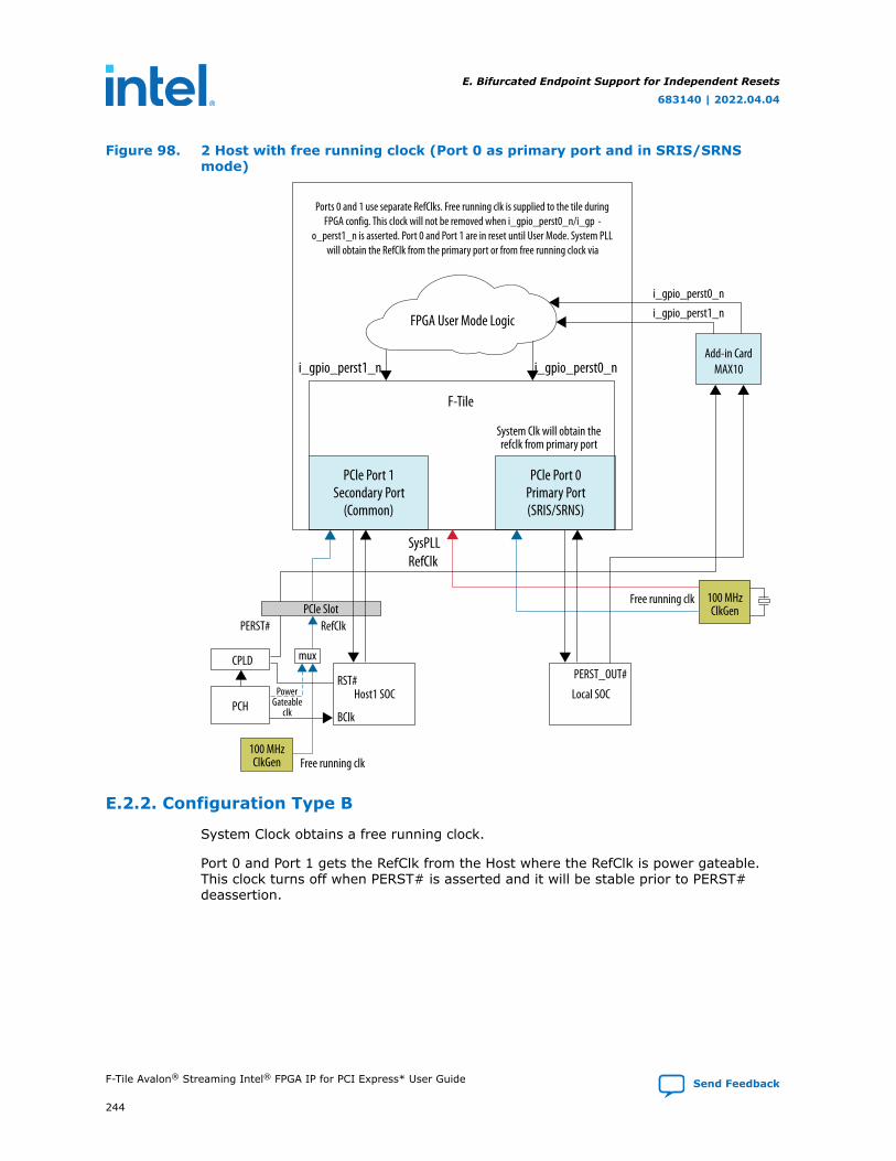
Figure 98. 2 Host with free running clock (Port 0 as primary port and in SRIS/SRNSmode)
i_gpio_perst1_n i_gpio_perst0_n
i_gpio_perst0_ni_gpio_perst1_n
System Clk will obtain therefclk from primary port
PowerGateable
clk
RefClkPERST#
PCle Port 0Primary Port(SRIS/SRNS)
Free running clk
Free running clk
FPGA User Mode Logic
Ports 0 and 1 use separate RefClks. Free running clk is supplied to the tile during FPGA config. This clock will not be removed when i_gpio_perst0_n/i_gp -
o_perst1_n is asserted. Port 0 and Port 1 are in reset until User Mode. System PLL will obtain the RefClk from the primary port or from free running clock via
PCle Port 1Secondary Port
(Common)
100 MHzClkGen
100 MHzClkGen
PCle Slot
mux
RST#
BClk
CPLD
Host1 SOCPCH
F-Tile
Add-in CardMAX10
PERST_OUT#
Local SOC
SysPLL RefClk
E.2.2. Configuration Type B
System Clock obtains a free running clock.
Port 0 and Port 1 gets the RefClk from the Host where the RefClk is power gateable.This clock turns off when PERST# is asserted and it will be stable prior to PERST#deassertion.
E. Bifurcated Endpoint Support for Independent Resets
683140 | 2022.04.04
F-Tile Avalon® Streaming Intel® FPGA IP for PCI Express* User Guide Send Feedback
244
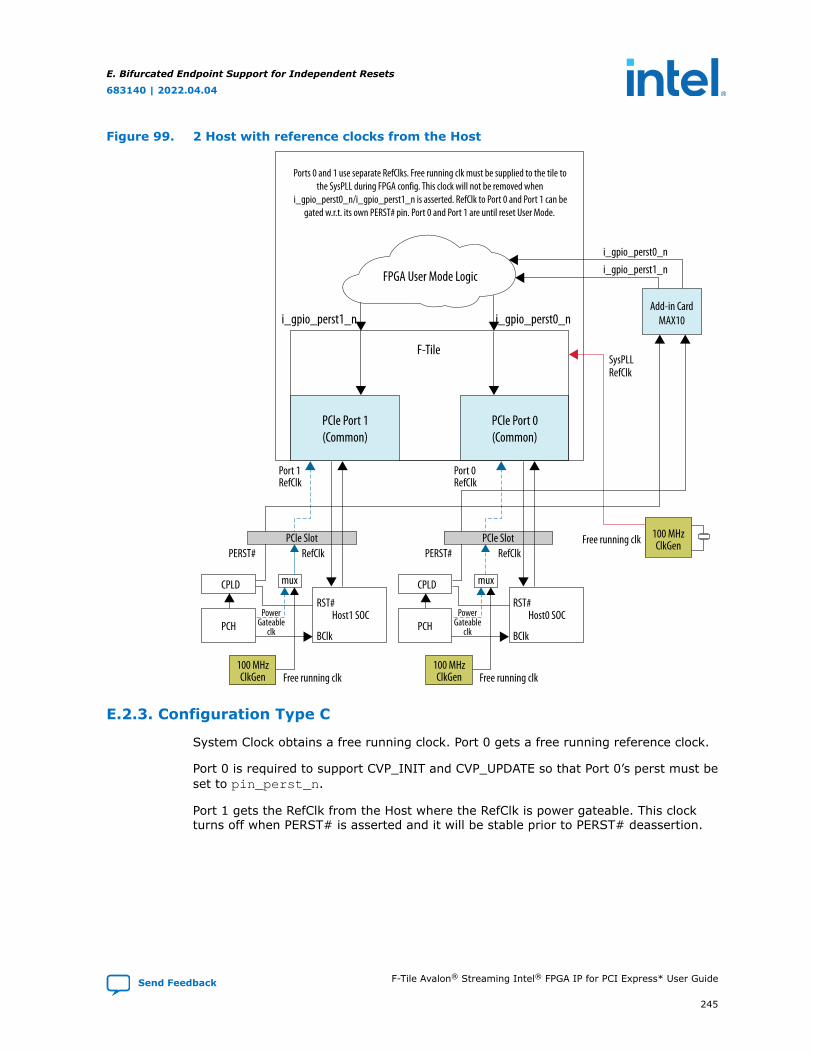
Figure 99. 2 Host with reference clocks from the Host
i_gpio_perst1_n i_gpio_perst0_n
i_gpio_perst0_ni_gpio_perst1_n
Port 0RefClk
Port 1RefClk
PowerGateable
clk
RefClkPERST#
PCle Port 0(Common)
Free running clk
PowerGateable
clk
RefClkPERST#
Free running clk
Free running clk
SysPLLRefClk
FPGA User Mode Logic
Ports 0 and 1 use separate RefClks. Free running clk must be supplied to the tile to the SysPLL during FPGA config. This clock will not be removed when
i_gpio_perst0_n/i_gpio_perst1_n is asserted. RefClk to Port 0 and Port 1 can be gated w.r.t. its own PERST# pin. Port 0 and Port 1 are until reset User Mode.
PCle Port 1(Common)
100 MHzClkGen
100 MHzClkGen
100 MHzClkGen
PCle SlotPCle Slot
mux
RST#
BClk
CPLD
Host1 SOCPCH
mux
RST#
BClk
CPLD
Host0 SOCPCH
F-Tile
Add-in CardMAX10
E.2.3. Configuration Type C
System Clock obtains a free running clock. Port 0 gets a free running reference clock.
Port 0 is required to support CVP_INIT and CVP_UPDATE so that Port 0’s perst must beset to pin_perst_n.
Port 1 gets the RefClk from the Host where the RefClk is power gateable. This clockturns off when PERST# is asserted and it will be stable prior to PERST# deassertion.
E. Bifurcated Endpoint Support for Independent Resets
683140 | 2022.04.04
Send Feedback F-Tile Avalon® Streaming Intel® FPGA IP for PCI Express* User Guide
245
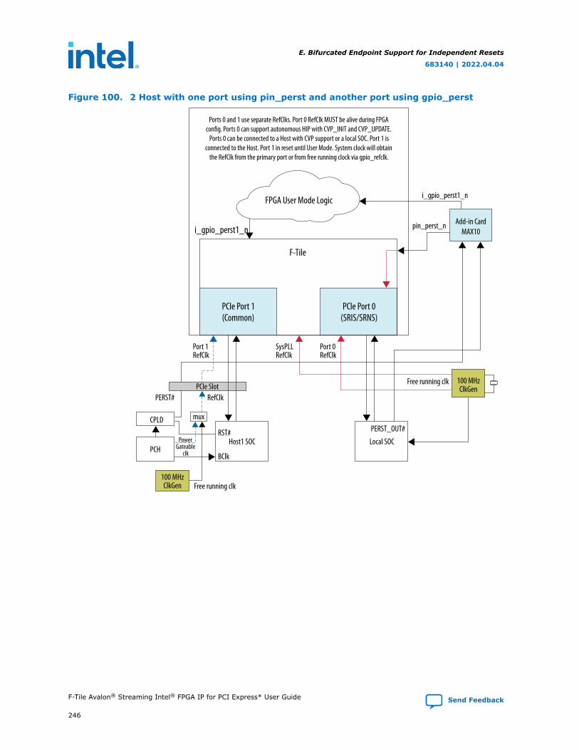
Figure 100. 2 Host with one port using pin_perst and another port using gpio_perst
i_gpio_perst1_n
pin_perst_n
PowerGateable
clk
RefClkPERST#
PCle Port 0(SRIS/SRNS)
Free running clk
Free running clk
FPGA User Mode Logic
Ports 0 and 1 use separate RefClks. Port 0 RefClk MUST be alive during FPGA config. Ports 0 can support autonomous HIP with CVP_INIT and CVP_UPDATE.
Ports 0 can be connected to a Host with CVP support or a local SOC. Port 1 is connected to the Host. Port 1 in reset until User Mode. System clock will obtain
the RefClk from the primary port or from free running clock via gpio_refclk.
PCle Port 1(Common)
100 MHzClkGen
100 MHzClkGen
PCle Slot
mux
RST#
BClk
CPLD
Host1 SOCPCH
F-Tile
Add-in CardMAX10
PERST_OUT#
Local SOC
Port 0RefClk
Port 1RefClk
SysPLLRefClk
i_gpio_perst1_n
E. Bifurcated Endpoint Support for Independent Resets
683140 | 2022.04.04
F-Tile Avalon® Streaming Intel® FPGA IP for PCI Express* User Guide Send Feedback
246
Related Documents