SN65HVD20, SN65HVD21 SN65HVD22, SN65HVD23, SN65HVD24 SLLS552B – DECEMBER 2002 – REVISED JUNE 2003 EXTENDED COMMON-MODE RS-485 TRANSCEIVERS FEATURES D Common-Mode Voltage Range (–20 V to 25 V) More Than Doubles TIA/EIA-485 Requirement D Reduced Unit-Load for up to 256 Nodes D Bus I/O Protection to Over 16-kV HBM D Failsafe Receiver for Open-Circuit, Short-Circuit and Idle-Bus Conditions D Low Standby Supply Current 1-µA Max D More Than 100 mV Receiver Hysteresis APPLICATIONS D Long Cable Solutions – Factory Automation – Security Networks – Building HVAC D Severe Electrical Environments – Electrical Power Inverters – Industrial Drives – Avionics DESCRIPTION The transceivers in the HVD2x family offer performance far exceeding typical RS–485 devices. In addition to meeting all requirements of the TIA/EIA–485–A standard, the HVD2x family operates over an extended range of common-mode voltage, and has features such as high ESD protection, wide receiver hysteresis, and failsafe operation. This family of devices is ideally suited for long-cable networks, and other applications where the environment is too harsh for ordinary transceivers. These devices are designed for bidirectional data transmission on multipoint twisted-pair cables. Example applications are digital motor controllers, remote sensors and terminals, industrial process control, security stations, and environmental control systems. These devices combine a 3-state differential driver and a differential receiver, which operate from a single 5-V power supply. The driver differential outputs and the receiver differential inputs are connected internally to form a differential bus port that offers minimum loading to the bus. This port features an extended common-mode voltage range making the device suitable for multipoint applications over long cable runs. –20 V +25 V –7 V +12 V SUPER–485 RS–485 –20 V –15 V –10 V –5 V 0 5 V 10 V 15 V 20 V 25 V HVD2x Devices Operate Over a Wider Common-Mode Voltage Range 0.1 1 10 100 10 100 1000 HVD20 HVD23 HVD24 HVD21 HVD22 Cable Length – m Signaling Rate – Mbps HVD2x APPLICATION SPACE PRODUCTION DATA information is current as of publication date. Products conform to specifications per the terms of Texas Instruments standard warranty. Production processing does not necessarily include testing of all parameters. Please be aware that an important notice concerning availability, standard warranty, and use in critical applications of Texas Instruments semiconductor products and disclaimers thereto appears at the end of this data sheet. www.ti.com Copyright 2002 – 2003, Texas Instruments Incorporated

Welcome message from author
This document is posted to help you gain knowledge. Please leave a comment to let me know what you think about it! Share it to your friends and learn new things together.
Transcript
SN65HVD20, SN65HVD21SN65HVD22, SN65HVD23, SN65HVD24
SLLS552B – DECEMBER 2002 – REVISED JUNE 2003
EXTENDED COMMON-MODE RS-485 TRANSCEIVERS
FEATURES
Common-Mode Voltage Range (–20 V to 25 V)More Than Doubles TIA/EIA-485 Requirement
Reduced Unit-Load for up to 256 Nodes
Bus I/O Protection to Over 16-kV HBM
Failsafe Receiver for Open-Circuit,Short-Circuit and Idle-Bus Conditions
Low Standby Supply Current 1-µA Max
More Than 100 mV Receiver Hysteresis
APPLICATIONS
Long Cable Solutions– Factory Automation– Security Networks– Building HVAC
Severe Electrical Environments– Electrical Power Inverters– Industrial Drives– Avionics
DESCRIPTION
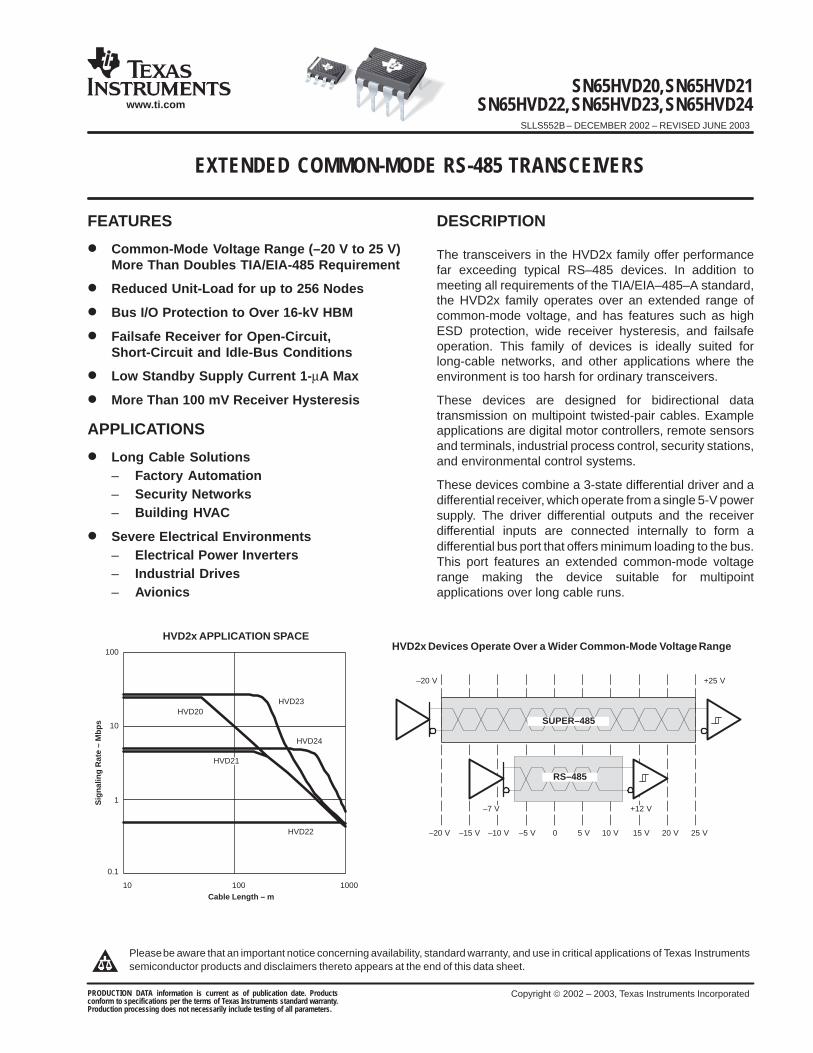
The transceivers in the HVD2x family offer performancefar exceeding typical RS–485 devices. In addition tomeeting all requirements of the TIA/EIA–485–A standard,the HVD2x family operates over an extended range ofcommon-mode voltage, and has features such as highESD protection, wide receiver hysteresis, and failsafeoperation. This family of devices is ideally suited forlong-cable networks, and other applications where theenvironment is too harsh for ordinary transceivers.
These devices are designed for bidirectional datatransmission on multipoint twisted-pair cables. Exampleapplications are digital motor controllers, remote sensorsand terminals, industrial process control, security stations,and environmental control systems.
These devices combine a 3-state differential driver and adifferential receiver, which operate from a single 5-V powersupply. The driver differential outputs and the receiverdifferential inputs are connected internally to form adifferential bus port that offers minimum loading to the bus.This port features an extended common-mode voltagerange making the device suitable for multipointapplications over long cable runs.
–20 V +25 V
–7 V +12 V
SUPER–485
RS–485
–20 V –15 V –10 V –5 V 0 5 V 10 V 15 V 20 V 25 V
HVD2x Devices Operate Over a Wider Common-Mode Voltage Range
0.1
1
10
100
10 100 1000
HVD20HVD23
HVD24
HVD21
HVD22
Cable Length – m
Sig
nal
ing
Rat
e –
Mb
ps
HVD2x APPLICATION SPACE
PRODUCTION DATA information is current as of publication date. Productsconform to specifications per the terms of Texas Instruments standard warranty.Production processing does not necessarily include testing of all parameters.
Please be aware that an important notice concerning availability, standard warranty, and use in critical applications of Texas Instrumentssemiconductor products and disclaimers thereto appears at the end of this data sheet.
www.ti.com
Copyright 2002 – 2003, Texas Instruments Incorporated
SN65HVD20, SN65HVD21SN65HVD22, SN65HVD23, SN65HVD24SLLS552B – DECEMBER 2002 – REVISED JUNE 2003
www.ti.com
2
These devices have limited built-in ESD protection. The leads should be shorted together or the device placed in conductive foam duringstorage or handling to prevent electrostatic damage to the MOS gates.
DESCRIPTION (continued)
The ‘HVD20 provides high signaling rate (up to 25 Mbps) for interconnecting networks of up to 64 nodes.
The ‘HVD21 allows up to 256 connected nodes at moderate data rates (up to 5 Mbps). The driver output slew rate iscontrolled to provide reliable switching with shaped transitions which reduce high-frequency noise emissions.
The ‘HVD22 has controlled driver output slew rate for low radiated noise in emission-sensitive applications and forimproved signal quality with long stubs. Up to 256 ‘HVD22 nodes can be connected at signaling rates up to 500 kbps.
The ‘HVD23 implements receiver equalization technology for improved jitter performance on differential bus applicationswith data rates up to 25 Mbps at cable lengths up to 160 meters.
The ‘HVD24 implements receiver equalization technology for improved jitter performance on differential bus applicationswith data rates in the range of 1 Mbps to 10 Mbps at cable lengths up to 1000 meters.
The receivers also include a failsafe circuit that provides a high-level output within 250 microseconds after loss of the inputsignal. The most common causes of signal loss are disconnected cables, shorted lines, or the absence of any activetransmitters on the bus. This feature prevents noise from being received as valid data under these fault conditions. Thisfeature may also be used for Wired-Or bus signaling.
The SN65HVD2X devices are characterized for operation over the temperature range of –40°C to 85°C.
PRODUCT SELECTION GUIDEPART NUMBERS CABLE LENGTH AND SIGNALING RATE(1) NODES MARKING
SN65HVD20 Up to 50 m at 25 Mbps Up to 64D: VP20P: 65HVD20
SN65HVD21 Up to 150 m at 5 Mbps (with slew rate limit) Up to 256D: VP21P: 65HVD21
SN65HVD22 Up to1200 m at 500 kbps (with slew rate limit) Up to 256D: VP22P: 65HVD22
SN65HVD23 Up to 160 m at 25 Mbps (with receiver equalization) Up to 64D: VP23P: 65HVD23
SN65HVD24 Up to 500 m at 3 Mbps (with receiver equalization) Up to 256D: VP24P: 65HVD24
(1) Distance and signaling rate predictions based upon Belden 3105A cable and 15% eye pattern jitter.
AVAILABLE OPTIONS
PLASTIC THROUGH-HOLEP–PACKAGE
(JEDEC MS-001)
PLASTIC SMALL-OUTLINE(1)
D–PACKAGE(JEDEC MS-012)
SN65HVD20PSN65HVD21PSN65HVD22PSN65HVD23PSN65HVD24P
SN65HVD20DSN65HVD21DSN65HVD22DSN65HVD23DSN65HVD24D
(1) Add R suffix for taped and reeled carriers.

SN65HVD20, SN65HVD21SN65HVD22, SN65HVD23, SN65HVD24
SLLS552B – DECEMBER 2002 – REVISED JUNE 2003
www.ti.com
3
DRIVER FUNCTION TABLEHVD20, HVD21, HVD22 HVD23, HVD24
INPUT ENABLE OUTPUTS INPUT ENABLE OUTPUTS
D DE A B D DE A B
H H H L H H H L
L H L H L H L H
X L Z Z X L Z Z
X OPEN Z Z X OPEN Z Z
OPEN H H L OPEN H L H
H = high level, L= low level, X = don’t care, Z = high impedance (off), ? = indeterminate
RECEIVER FUNCTION TABLE
DIFFERENTIAL INPUT ENABLE OUTPUT
VID = (VA – VB) RE R
0.2 V ≤ VID L H
–0.2 V < VID < 0.2 V L See Note A
VID ≤ –0.2 V L L
X H Z
X OPEN Z
Open circuit L H
Short Circuit L H
Idle (terminated) bus L H
H = high level, L= low level, X = don’t care,Z = high impedance (off), ? = indeterminate
NOTE A: If the differential input VID remains within the indeterminate-logicrange for more than 250 µs, the integrated failsafe circuitry detectsa bus fault, and set the receiver output to a high state. SeeFigure 15.

SN65HVD20, SN65HVD21SN65HVD22, SN65HVD23, SN65HVD24SLLS552B – DECEMBER 2002 – REVISED JUNE 2003
www.ti.com
4
POWER DISSIPATION RATINGS
PACKAGECIRCUIT BOARD
MODELTA ≤ 25°C
POWER RATINGDERATING FACTOR(3)
ABOVE TA = 25°CTA = 70°C
POWER RATINGTA = 85°C
POWER RATING
DLow-K(1) 710 mW 5.68 mW/°C 455 mW 370 mW
DHigh-K(2) 1282 mW 10.3 mW/°C 821 mW 667 mW
PLow-K(1) 984 mW 7.87 mW/°C 630 mW 512 mW
PHigh-K(2) 1478 mW 11.8 mW/°C 946 mW 768 mW
(1) In accordance with the Low-K thermal metric definitions of EIA/JESD51–3.(2) In accordance with the High-K thermal metric definitions of EIA/JESD51–7.(3) This is the inverse of the junction-to-ambient thermal resistance when board-mounted and with no air flow.
ABSOLUTE MAXIMUM RATINGSover operating free-air temperature range unless otherwise noted(1)
SN65HVD2X
Supply voltage(2), VCC –0.5 V to 7 V
Voltage at any bus I/O terminal –27 V to 27 V
Voltage input, transient pulse, A and B, (through 100 Ω, see Figure 16) –60 V to 60 V
Voltage input at any D, DE or RE terminal –0.5 V to VCC+ 0.5 V
Human Body Model(3)A, B, GND 16 kV
Electrostatic discharge
Human Body Model(3)All pins 5 kV
Electrostatic dischargeCharged-Device Model(4) All pins 1.5 kV
Machine Model(5) All pins 200 V
Continuous total power dissipation See Power Dissipation Rating Table
Junction temperature, TJ 150°C
Storage temperature, Tstg –65°C to 120°C(1) Stresses beyond those listed under “absolute maximum ratings” may cause permanent damage to the device. These are stress ratings only, and
functional operation of the device at these or any other conditions beyond those indicated under “recommended operating conditions” is notimplied. Exposure to absolute-maximum-rated conditions for extended periods may affect device reliability.
(2) All voltage values, except differential I/O bus voltages, are with respect to network ground terminal.(3) Tested in accordance with JEDEC Standard 22, Test Method A114-A.(4) Tested in accordance with JEDEC Standard 22, Test Method C101.(5) Tested in accordance with JEDEC Standard 22, Test Method A115-A.
RECOMMENDED OPERATING CONDITIONSMIN NOM MAX UNIT
Supply voltage, VCC 4.5 5 5.5 V
Voltage at any bus I/O terminal A, B –20 25 V
High-level input voltage, VIHD, DE, RE
2 VCCV
Low-level input voltage, VILD, DE, RE
0 0.8V
Differential input voltage, VID A with respect to B –25 25 V
Output currentDriver –110 110
mAOutput currentReceiver –8 8
mA
Operating free-air temperature, TA –40 85 °C
Junction temperature, TJ –40 125 °C

SN65HVD20, SN65HVD21SN65HVD22, SN65HVD23, SN65HVD24
SLLS552B – DECEMBER 2002 – REVISED JUNE 2003
www.ti.com
5
DRIVER ELECTRICAL CHARACTERISTICSover recommended operating conditions (unless otherwise noted)(1)
PARAMETER TEST CONDITIONS MIN TYP(1) MAX UNIT
VIK Input clamp voltage II = –18 mA –1.5 0.75 V
VO Open-circuit output voltage A or B, No load 0 VCC V
Steady-state differential output voltageNo load (open circuit) 3.3 4.2 VCC
VOD(SS)Steady-state differential output voltagemagnitude
RL = 54 Ω, See Figure 1 1.8 2.5 VVOD(SS) magnitudeWith common-mode loading, See Figure 2 1.8
V
∆|VOD(SS)| Change in steady-state differential outputvoltage between logic states
See Figure 1 and Figure 3 –0.1 0.1 V
VOC(SS) Steady-state common-mode output voltage See Figure 1 2.1 2.5 2.9 V
∆VOC(SS)Change in steady-state common-mode outputvoltage, VOC(H) – VOC(L)
See Figure 1 and Figure 4 –0.1 0.1 V
VOC(PP)Peak-to-peak common-mode output voltage,VOC(MAX) – VOC(MIN)
RL = 54 Ω, CL = 50 pF,See Figure 1 and Figure 4
0.35 V
VOD(RING) Differential output voltage over and under shoot RL = 54 Ω, CL = 50 pF, See Figure 5 10%
II Input current D, DE –100 100 µA
IO(OFF) Output current with power off VCC < = 2.5 V See receiver line inputIOZ High impedance state output current DE at 0 V
See receiver line inputcurrent
IOS Short-circuit output current VO = –20 V to 25 V, See Figure 9 –250 250 mA
COD Differential output capacitance See receiver CI(1) All typical values are at VCC = 5 V and 25°C.
DRIVER SWITCHING CHARACTERISTICS over recommended operating conditions (unless otherwise noted)
PARAMETER TEST CONDITIONS MIN TYP(1) MAX UNIT
t Differential output propagation delay, low-to- high R = 54 , HVD20, HVD23 6 10 20tPLH Differential output propagation delay, low-to- high RL = 54 Ω, HVD20, HVD23 6 10 20tPLH Differential output propagation delay, low-to- high RL = 54 Ω,CL = 50 pF, HVD21, HVD24 20 32 60 ns
t Differential output propagation delay, high-to-lowCL = 50 pF,See Figure 3
HVD21, HVD24 20 32 60 nstPHL Differential output propagation delay, high-to-low
CL = 50 pF,See Figure 3 HVD22 160 280 500
nstPHL Differential output propagation delay, high-to-low See Figure 3 HVD22 160 280 500
t Differential output rise time R = 54 , HVD20, HVD23 2 6 12tr Differential output rise time RL = 54 Ω, HVD20, HVD23 2 6 12tr Differential output rise time RL = 54 Ω,CL = 50 pF, HVD21, HVD24 20 40 60 ns
t Differential output fall timeCL = 50 pF,See Figure 3
HVD21, HVD24 20 40 60 nstf Differential output fall time
CL = 50 pF,See Figure 3 HVD22 200 400 600
nstf Differential output fall time See Figure 3 HVD22 200 400 600
t Propagation delay time, high-impedance-to-high-level output HVD20, HVD23 40tPZH Propagation delay time, high-impedance-to-high-level outputRE at 0 V,
HVD20, HVD23 40tPZH Propagation delay time, high-impedance-to-high-level outputRE at 0 V,
HVD21, HVD24 100 nst Propagation delay time, high-level-output-to-high-impedance
RE at 0 V,See Figure 6
HVD21, HVD24 100 nstPHZ Propagation delay time, high-level-output-to-high-impedance
See Figure 6HVD22 300
nstPHZ Propagation delay time, high-level-output-to-high-impedance
See Figure 6HVD22 300
t Propagation delay time, high-impedance-to-low-level output HVD20, HVD23 40tPZL Propagation delay time, high-impedance-to-low-level outputRE at 0 V,
HVD20, HVD23 40tPZL Propagation delay time, high-impedance-to-low-level outputRE at 0 V,
HVD21, HVD24 100 nst Propagation delay time, low-level-output-to-high-impedance
RE at 0 V,See Figure 7
HVD21, HVD24 100 nstPLZ Propagation delay time, low-level-output-to-high-impedance
See Figure 7HVD22 300
nstPLZ Propagation delay time, low-level-output-to-high-impedance
See Figure 7HVD22 300
td(standby) Time from an active differential output to standbyRE at VCC, See Figure 8
2 µs
td(wake) Wake-up time from standby to an active differential outputRE at VCC, See Figure 8
8 µs
HVD20, HVD23 2
tsk(p) Pulse skew | tPLH – tPHL | HVD21, HVD24 6 nstsk(p) Pulse skew | tPLH – tPHL |
HVD22 50
ns
(1) All typical values are at VCC = 5 V and 25°C.

SN65HVD20, SN65HVD21SN65HVD22, SN65HVD23, SN65HVD24SLLS552B – DECEMBER 2002 – REVISED JUNE 2003
www.ti.com
6
RECEIVER ELECTRICAL CHARACTERISTICSover recommended operating conditions
PARAMETER TEST CONDITIONS MIN TYP(1) MAX UNIT
VIT(+) Positive-going differential input voltage thresholdSee Figure 10
VO = 2.4 V, IO = –8 mA 60 200mV
VIT(–) Negative-going differential input voltage thresholdSee Figure 10
VO = 0.4 V, IO = 8 mA –200 –60mV
VHYS Hysteresis voltage (VIT+ – VIT–) 100 130 mV
VIT(F+)Positive-going differential input failsafe voltage
See Figure 15VCM = –7 V to 12 V 40 120 200
mVVIT(F+)Positive-going differential input failsafe voltagethreshold
See Figure 15VCM = –20 V to 25 V 120 250
mV
VIT(F–)Negative-going differential input failsafe voltage
See Figure 15VCM = –7 V to 12 V –200 –120 –40
mVVIT(F–)Negative-going differential input failsafe voltagethreshold
See Figure 15VCM = –20 V to 25 V –250 –120
mV
VIK Input clamp voltage II = –18 mA –1.5 V
VOH High-level output voltage VID = 200 mV, IOH = –8 mA, See Figure 11 4 V
VOL Low-level output voltage VID = –200 mV, IOL = 8 mA, See Figure 11 0.4 V
VI = –7 to 12 V, HVD20, HVD23 –400 500
II(BUS) Bus input current (power on or power off)
VI = –7 to 12 V,Other input = 0 V HVD21, HVD22, HVD24 –100 125
µAII(BUS) Bus input current (power on or power off)VI = –20 to 25 V, HVD20, HVD23 –800 1000
µAVI = –20 to 25 V,Other input = 0 V HVD21, HVD22, HVD24 –200 250
II Input current RE –100 100 µA
RI Input resistanceHVD20, 23 24
kΩRI Input resistanceHVD21, 22, 24 96
kΩ
CID Differential input capacitance VID = 0.5 + 0.4 sine (2π x 1.5 x 106t) 20 pF(1) All typical values are at 25°C.
RECEIVER SWITCHING CHARACTERISTICS over recommended operating conditions
PARAMETER TEST CONDITIONS MIN TYP MAX UNIT
tPLH Propagation delay time, low-to-high level outputSee Figure 11
HVD20, HVD23 16 35ns
tPHL Propagation delay time, high-to-low level outputSee Figure 11
HVD21, HVD22, HVD24 25 50ns
tPHL Propagation delay time, high-to-low level outputSee Figure 11
HVD21, HVD22, HVD24 25 50ns
tr Receiver output rise timeSee Figure 11 2 4 ns
tf Receiver output fall timeSee Figure 11 2 4 ns
tPZH Receiver output enable time to high levelSee Figure 12
90 120ns
tPHZ Receiver output disable time from high levelSee Figure 12
16 35ns
tPZL Receiver output enable time to low levelSee Figure 13
90 120ns
tPLZ Receiver output disable time from low levelSee Figure 13
16 35ns
tr(standby) Time from an active receiver output to standby 2
tr(wake)Wake-up time from standby to an active receiveroutput
See Figure 14, DE at 0 V8
µs
tsk(p) Pulse skew | tPLH – tPHL | 5 nstsk(p) Pulse skew | tPLH – tPHL | 5 nstsk(p) Pulse skew | tPLH – tPHL | 5 nstp(set) Delay time, bus fail to failsafe set
See Figure 15, pulse rate = 1 kHz250 350 µs
tp(reset) Delay time, bus recovery to failsafe resetSee Figure 15, pulse rate = 1 kHz
50 ns

SN65HVD20, SN65HVD21SN65HVD22, SN65HVD23, SN65HVD24
SLLS552B – DECEMBER 2002 – REVISED JUNE 2003
www.ti.com
7
RECEIVER EQUALIZATION CHARACTERISTICS(1) over recommended operating conditions
PARAMETER TEST CONDITIONS MIN TYP(2) MAX UNIT
0 m HVD23 2
100 m(3)HVD20 6
100 m(3)HVD23 3
25 Mbps150 m
HVD20 1525 Mbps150 m
HVD23 4
200 mHVD20 27
200 mHVD23 8
200 mHVD20 22
200 mHVD23 8
Peak-to-peakPseudo-random NRZ code with a
16 10 Mbps 250 mHVD20 34
tj(pp)Peak-to-peakeye-patttern jitter
Pseudo-random NRZ code with abit pattern length of 216 – 1 ,See Figure 26
10 Mbps 250 mHVD23 15 nstj(pp) eye-patttern jitter
bit pattern length of 216 – 1 ,See Figure 26
300 mHVD20 49
ns
300 mHVD23 27
5 Mbps 500 mHVD21 128
5 Mbps 500 mHVD24 18
HVD20 93
3 Mbps 500 mHVD21 103
3 Mbps 500 mHVD23 90
HVD24 16
1 Mbps 1000 mHVD21 216
1 Mbps 1000 mHVD24 62
(1) The HVD20 and HVD21 do not have receiver equalization, but are specified for comparison.(2) All typical values are at VCC = 5 V, and temperature = 25°C.(3) Cable is Belden 3105A or equivalent.
SUPPLY CURRENTover recommended operating conditions (unless otherwise noted)
PARAMETER TEST CONDITIONS MIN TYP MAX UNIT
HVD20 6 9
Driver enabled (DE at VCC), HVD21 8 12Driver enabled (DE at VCC),Receiver enabled (RE at 0 V)No load, V = 0 V or V
HVD22 6 9 mAReceiver enabled (RE at 0 V)No load, VI = 0 V or VCC HVD23 7 11
mAI CC
HVD24 10 14
HVD20 5 8
Driver enabled (DE at VCC), HVD21 7 11Driver enabled (DE at VCC),Receiver disabled (RE at VCC)No load, V = 0 V or V
HVD22 5 8 mA
ICC Supply current
Receiver disabled (RE at VCC)No load, VI = 0 V or VCC HVD23 5 9
mA
ICC Supply current I CC
HVD24 8 12
HVD20 4 7
Driver disabled (DE at 0 V), HVD21 5 8Driver disabled (DE at 0 V),Receiver enabled (RE at 0 V)No load
HVD22 4 7 mAReceiver enabled (RE at 0 V)No load HVD23 4.5 9
mA
HVD24 5.5 10
Driver disabled (DE at 0 V)Receiver disabled (RE at VCC)D open
All HVD2x 1 µA

SN65HVD20, SN65HVD21SN65HVD22, SN65HVD23, SN65HVD24SLLS552B – DECEMBER 2002 – REVISED JUNE 2003
www.ti.com
8
EQUIVALENT INPUT AND OUTPUT SCHEMATIC DIAGRAMS
9 V
1 kΩ
100 kΩ
Input
VCC
RE Inputs
9 V
1 kΩ
100 kΩ
Input
VCC
DE Input
29 V
R3R1
R2
Input
A Input
29 V
R3R1
R2
Input
B Input
29 V
VCC
A and B Outputs
9 V
VCC
R Output
5 ΩOutput
VCC
HVD20, 23
HVD21, 22, 24
R1/R2
9 kΩ36 kΩ
R3
45 kΩ180 kΩ
VCC
Output
D Inputs (HVD20, 21, 22) D Inputs (HVD23, 24)
SN65HVD20, SN65HVD21SN65HVD22, SN65HVD23, SN65HVD24
SLLS552B – DECEMBER 2002 – REVISED JUNE 2003
www.ti.com
9
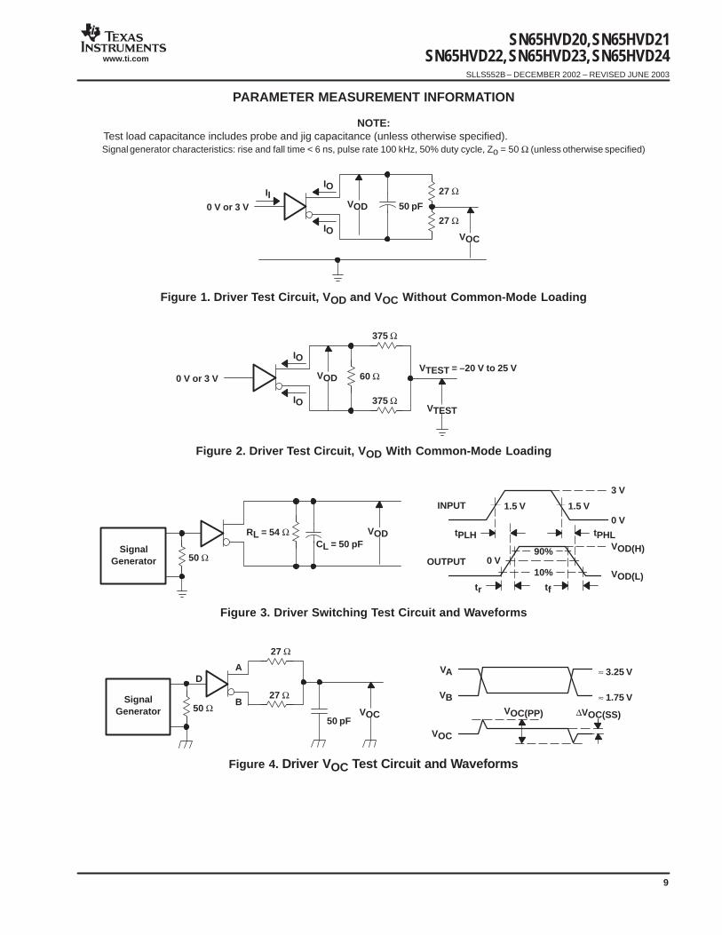
PARAMETER MEASUREMENT INFORMATION
NOTE:Test load capacitance includes probe and jig capacitance (unless otherwise specified). Signal generator characteristics: rise and fall time < 6 ns, pulse rate 100 kHz, 50% duty cycle, Zo = 50 Ω (unless otherwise specified)
IIIO
IO
VOD 50 pF
27 Ω
27 Ω
VOC
0 V or 3 V
Figure 1. Driver Test Circuit, VOD and VOC Without Common-Mode Loading
IO
IO
VOD 60 Ω
VTEST
0 V or 3 V
375 Ω
375 Ω
VTEST = –20 V to 25 V
Figure 2. Driver Test Circuit, VOD With Common-Mode Loading
VOD
50 Ω
RL = 54 ΩCL = 50 pFSignal
Generator
1.5 V 1.5 V
3 V
0 VtPLH tPHL
VOD(H)
VOD(L)
90%0 V
10%
tr tf
INPUT
OUTPUT
Figure 3. Driver Switching Test Circuit and Waveforms
VOC50 Ω
SignalGenerator
A
B
27 Ω
27 Ω
50 pF
DVA
VB
VOC
VOC(PP) ∆VOC(SS)
≈ 3.25 V
≈ 1.75 V
Figure 4. Driver VOC Test Circuit and Waveforms

SN65HVD20, SN65HVD21SN65HVD22, SN65HVD23, SN65HVD24SLLS552B – DECEMBER 2002 – REVISED JUNE 2003
www.ti.com
10
VOD(PP)
VOD(RING)
VOD(RING)
VOD(SS)
VOD(SS)
0 V Differential
NOTE: VOD(RING) is measured at four points on the output waveform, corresponding to overshoot and undershoot from theVOD(H) and VOD(L) steady state values.
Figure 5. VOD(RING) Waveform and Definitions
50 Ω
CL = 50 pF
SignalGenerator
DE
D0 V or 3 V
3 V if Testing A Output0 V if Testing B Output
A
B
RL = 110 Ω
OutputS1
tPZH
tPHZ
0.5 V
DE
Output
1.5 V 1.5 V
2.5 V
3 V
0 V
VOH
VOff 0
Figure 6. Driver Enable/Disable Test, High Output
50 Ω
CL = 50 pF
SignalGenerator
DE
D0 V or 3 V
0 V if Testing A Output3 V if Testing B Output
RL = 110 Ω
Output
S1
tPZLtPLZ
0.5 V
DE
Output
1.5 V 1.5 V
2.5 V
3 V
0 V
5 V
VOL
5 V
Figure 7. Driver Enable/Disable Test, Low Output
VODRL = 54 Ω CL = 50 pF
50 ΩSignal
Generator
DE
D0 V or 3 V
A
B
3 V1.5 V0 V
0.2 V
1.5 V
td(Wake)td(Standby)
DE
VOD
Figure 8. Driver Standby/Wake Test Circuit and Waveforms

SN65HVD20, SN65HVD21SN65HVD22, SN65HVD23, SN65HVD24
SLLS552B – DECEMBER 2002 – REVISED JUNE 2003
www.ti.com
11
VoltageSource
IOS
VO
Figure 9. Driver Short-Circuit Test
IO
VO
VID
Figure 10. Receiver DC Parameter Definitions
50 ΩSignal
Generator
CL = 15 pF50 Ω
SignalGenerator
A
VID
BR
IO
VO
50%
90%
10%
1.5 V
0 V
VOH
VOL
tPLH tPHL
tr tf
Input B
Input A
Output 1.5 V
Figure 11. Receiver Switching Test Circuit and Waveforms
50 ΩSignal
Generator
RE
B
A
54 Ω
CL = 15 pF
R 1 kΩ0 V
VCCVCC
D
DE
RE
R
1.5 V
tPZH tPHZ
3 V
0 V
VOHVOH –0.5 V
GND1.5 V
Figure 12. Receiver Enable Test Circuit and Waveforms, Data Output High

SN65HVD20, SN65HVD21SN65HVD22, SN65HVD23, SN65HVD24SLLS552B – DECEMBER 2002 – REVISED JUNE 2003
www.ti.com
12
50 ΩSignal
Generator
RE
B
A
54 Ω
CL = 15 pF
R 1 kΩ5 V
0 V
VCC
D
DE
RE
R
1.5 V
tPZL tPLZ
3 V
0 V
VCC
VOL +0.5 V1.5 VVOL
Figure 13. Receiver Enable Test Circuit and Waveforms, Data Output Low
1.5 V
50 ΩSignal
Generator
RE
B
A
CL = 15 pF
R1 kΩ
Switch Down for V(A) = 1.5 V,Switch Up for V(A) = –1.5 V
VCC
1.5 V or–1.5 V
tr(Wake) tr(Standby)
RE
5 V
0 V
1.5 VVOH –0.5 VVOL +0.5 V
3 V
0 V
VOH
VOLR
Figure 14. Receiver Standby and Wake Test Circuit and Waveforms
Bus Data Valid Region
Bus DataIndeterminate Region
Bus Data Valid Region
tp(SET) tp(RESET)
200 mV
–40 mV–200 mV
–1.5 V
VOH
VOL
1.5 V
VID
R
Figure 15. Receiver Active Failsafe Definitions and Waveforms
Pulse Generator,15 µs Duration,1% Duty Cycle
100 ΩVTEST
0 V
15 µs 1.5 ms –VTEST
Figure 16. Test Circuit and Waveforms, Transient Overvoltage Test

SN65HVD20, SN65HVD21SN65HVD22, SN65HVD23, SN65HVD24
SLLS552B – DECEMBER 2002 – REVISED JUNE 2003
www.ti.com
13
PIN ASSIGNMENTS
1
2
3
4
8
7
6
5
RREDE
D
VCCBAGND
D or P PACKAGE(TOP VIEW)
LOGIC DIAGRAM
POSITIVE LOGIC
6
7A
B3
4
2
1
DE
D
RE
R
TYPICAL CHARACTERISTICS
Figure 17
–600
–400
–200
0
200
400
600
–30 –20 –10 0 10 20 30
VCC = 0 V
VCC = 5 V
Bu
s P
in C
urr
ent –
Bus Pin Voltage – V
HVD20, HVD23BUS PIN CURRENT
vsBUS PIN VOLTAGE
Aµ
DE = 0 V
Figure 18
–150
–100
–50
0
50
100
150
–30 –20 –10 0 10 20 30
VCC = 0 V
VCC = 5 V
Bu
s P
in C
urr
ent –
Bus Pin Voltage – V
HVD21, HVD22, HVD24BUS PIN CURRENT
vsBUS PIN VOLTAGE
Aµ
DE = 0 V
SN65HVD20, SN65HVD21SN65HVD22, SN65HVD23, SN65HVD24SLLS552B – DECEMBER 2002 – REVISED JUNE 2003
www.ti.com
14
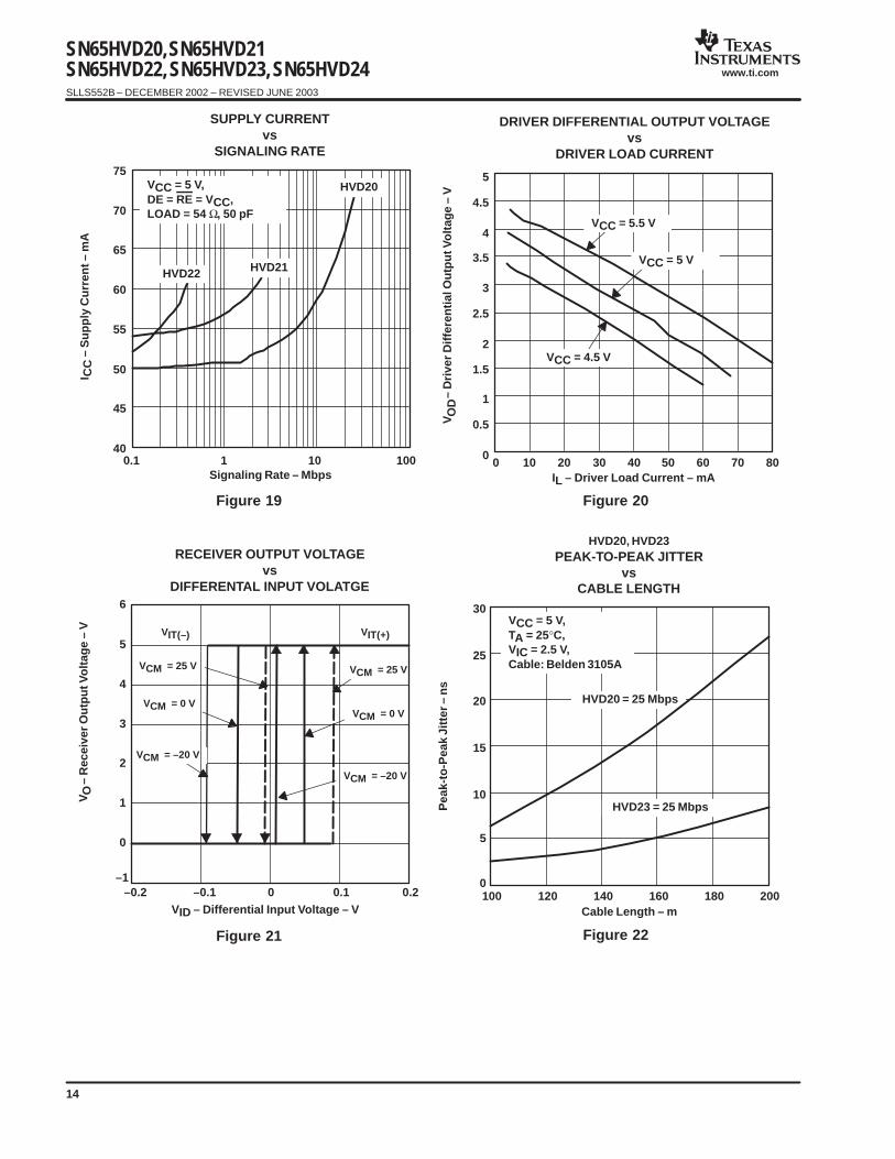
Figure 19
40
45
50
55
60
65
70
75
0.1 1 10 100
HVD22 HVD21
HVD20VCC = 5 V,DE = RE = VCC,LOAD = 54 Ω, 50 pF
I CC
– S
up
ply
Cu
rren
t – m
A
Signaling Rate – Mbps
SUPPLY CURRENTvs
SIGNALING RATE
Figure 20
0
0.5
1
1.5
2
2.5
3
3.5
4
4.5
5
0 10 20 30 40 50 60 70 80
VCC = 5.5 V
VCC = 5 V
VCC = 4.5 V
– D
rive
r D
iffe
ren
tial
Ou
tpu
t Vo
ltag
e –
V
DRIVER DIFFERENTIAL OUTPUT VOLTAGEvs
DRIVER LOAD CURRENT
VO
D
IL – Driver Load Current – mA
Figure 21
–1
0
1
2
3
4
5
6
–0.2 –0.1 0 0.1 0.2
VCM = 25 V
VCM = 0 V
VCM = –20 V
VCM = 25 V
VCM = 0 V
VCM = –20 V
– R
ecei
ver
Ou
tpu
t Vo
ltag
e –
VV
O
VID – Differential Input Voltage – V
RECEIVER OUTPUT VOLTAGEvs
DIFFERENTAL INPUT VOLATGE
VIT(–) VIT(+)
Figure 22
0
5
10
15
20
25
30
100 120 140 160 180 200
HVD20 = 25 Mbps
Pea
k-to
-Pea
k Ji
tter
– n
s
Cable Length – m
HVD20, HVD23PEAK-TO-PEAK JITTER
vsCABLE LENGTH
HVD23 = 25 Mbps
VCC = 5 V,TA = 25°C,VIC = 2.5 V,Cable: Belden 3105A

SN65HVD20, SN65HVD21SN65HVD22, SN65HVD23, SN65HVD24
SLLS552B – DECEMBER 2002 – REVISED JUNE 2003
www.ti.com
15
Figure 23
0
10
20
30
40
50
60
70
200 220 240 260 280 300
HVD21 = 10 Mbps
HVD20 = 10 Mbps
HVD23 = 10 Mbps
HVD24 = 10 Mbps
Pea
k-to
-Pea
k Ji
tter
– n
s
Cable Length – m
HVD20, HVD21, HVD23, HVD24PEAK-TO-PEAK JITTER
vsCABLE LENGTH
VCC = 5 V,TA = 25°C,VIC = 2.5 V,Cable: Belden 3105A
Figure 24
10
30
50
70
90
110
130
3 3.5 4 4.5 5
HVD21: 500 m Cable
Pea
k-to
-Pea
k Ji
tter
– n
sSignaling Rate – Mbps
HVD20, HVD23PEAK-TO-PEAK JITTER
vsSIGNALING RATE
VCC = 5 V,TA = 25°C,VIC = 2.5 V,Cable: Belden 3105A
HVD24: 500 m Cable

SN65HVD20, SN65HVD21SN65HVD22, SN65HVD23, SN65HVD24SLLS552B – DECEMBER 2002 – REVISED JUNE 2003
www.ti.com
16
APPLICATION INFORMATION
Figure 25. HVD22 Receiver Operation With 20 V Offset on Input Signal
H(s) k01–k1
k1p1s p1
1–k2
k2p2s p2
1–k3
k3p3s p3
k0
(DCloss)
p1(MHz)
k1p2
(MHz)k2
p3(MHz)
k3
Similar to 160m of Belden 3105A 0.95 0.25 0.3 3.5 0.5 15 1
Similar to 250m of Belden 3105A 0.9 0.25 0.4 3.5 0.7 12 1
Similar to 500m of Belden 3105A 0.8 0.25 0.6 2.2 1 8 1
Similar to 1000m of Belden 3105A 0.6 0.3 1 3 1 6 1
H(s)Signal
Generator
Figure 26. Cable Attenuation Model for Jitter Measurements

SN65HVD20, SN65HVD21SN65HVD22, SN65HVD23, SN65HVD24
SLLS552B – DECEMBER 2002 – REVISED JUNE 2003
www.ti.com
17
INTEGRATED RECEIVER EQUALIZATION USING THE HVD23
Figure 27 illustrates the benefits of integrated receiver equalization as implemented in the HVD23 transceiver.In this test setup, a differential signal generator applied a signal voltage at one end of the cable, which wasBelden 3105A twisted-pair shielded cable. The test signal was a pseudo-random bit stream (PRBS) ofnonreturn-to-zero (NRZ) data. Channel 1 (top) shows the eye-pattern of the differential voltage at the receiverinputs (after the cable attenuation). Channel 2 (bottom) shows the output of the receiver.
Figure 27. HVD23 Receiver Performance at 25 Mbps Over 150 Meter Cable

SN65HVD20, SN65HVD21SN65HVD22, SN65HVD23, SN65HVD24SLLS552B – DECEMBER 2002 – REVISED JUNE 2003
www.ti.com
18
INTEGRATED RECEIVER EQUALIZATION USING THE HVD24
Figure 28 illustrates the benefits of integrated receiver equalization as implemented in the HVD24 transceiver.In this test setup, a differential signal generator applied a signal voltage at one end of the cable, which wasBelden 3105A twisted-pair shielded cable. The test signal was a pseudo-random bit stream (PRBS) ofnonreturn-to-zero (NRZ) data. Channel 1 (top) shows the eye-pattern of the bit stream. Channel 2 (middle)shows the eye-pattern of the differential voltage at the receiver inputs (after the cable attenuation). Channel3 (bottom) shows the output of the receiver.
Figure 28. HVD24 Receiver Performance at 5 Mbps Over 500 Meter Cable
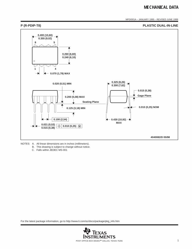
MECHANICAL DATA
MPDI001A – JANUARY 1995 – REVISED JUNE 1999
1POST OFFICE BOX 655303 • DALLAS, TEXAS 75265
P (R-PDIP-T8) PLASTIC DUAL-IN-LINE
8
4
0.015 (0,38)
Gage Plane
0.325 (8,26)0.300 (7,62)
0.010 (0,25) NOM
MAX0.430 (10,92)
4040082/D 05/98
0.200 (5,08) MAX
0.125 (3,18) MIN
5
0.355 (9,02)
0.020 (0,51) MIN
0.070 (1,78) MAX
0.240 (6,10)0.260 (6,60)
0.400 (10,60)
1
0.015 (0,38)0.021 (0,53)
Seating Plane
M0.010 (0,25)
0.100 (2,54)
NOTES: A. All linear dimensions are in inches (millimeters).B. This drawing is subject to change without notice.C. Falls within JEDEC MS-001
For the latest package information, go to http://www.ti.com/sc/docs/package/pkg_info.htm
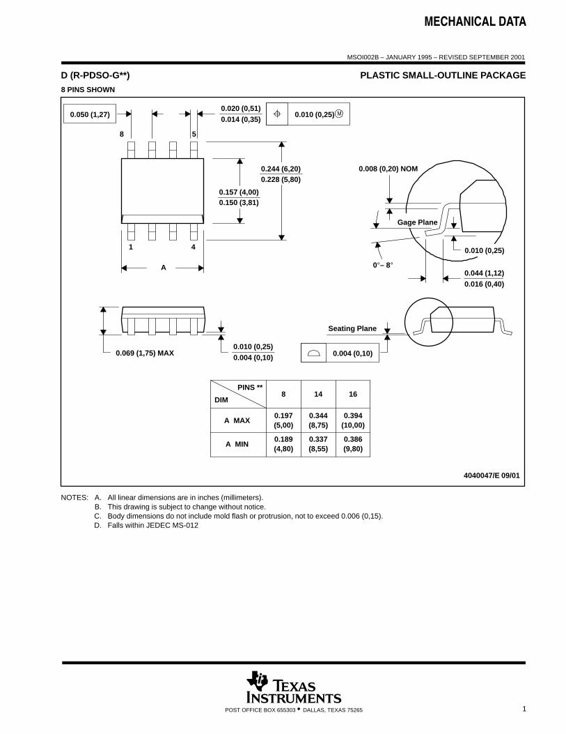
MECHANICAL DATA
MSOI002B – JANUARY 1995 – REVISED SEPTEMBER 2001
1POST OFFICE BOX 655303 • DALLAS, TEXAS 75265
D (R-PDSO-G**) PLASTIC SMALL-OUTLINE PACKAGE8 PINS SHOWN
8
0.197(5,00)
A MAX
A MIN(4,80)0.189 0.337
(8,55)
(8,75)0.344
14
0.386(9,80)
(10,00)0.394
16DIM
PINS **
4040047/E 09/01
0.069 (1,75) MAX
Seating Plane
0.004 (0,10)0.010 (0,25)
0.010 (0,25)
0.016 (0,40)0.044 (1,12)
0.244 (6,20)0.228 (5,80)
0.020 (0,51)0.014 (0,35)
1 4
8 5
0.150 (3,81)0.157 (4,00)
0.008 (0,20) NOM
0°– 8°
Gage Plane
A
0.004 (0,10)
0.010 (0,25)0.050 (1,27)
NOTES: A. All linear dimensions are in inches (millimeters).B. This drawing is subject to change without notice.C. Body dimensions do not include mold flash or protrusion, not to exceed 0.006 (0,15).D. Falls within JEDEC MS-012

IMPORTANT NOTICE
Texas Instruments Incorporated and its subsidiaries (TI) reserve the right to make corrections, modifications,enhancements, improvements, and other changes to its products and services at any time and to discontinueany product or service without notice. Customers should obtain the latest relevant information before placingorders and should verify that such information is current and complete. All products are sold subject to TI’s termsand conditions of sale supplied at the time of order acknowledgment.
TI warrants performance of its hardware products to the specifications applicable at the time of sale inaccordance with TI’s standard warranty. Testing and other quality control techniques are used to the extent TIdeems necessary to support this warranty. Except where mandated by government requirements, testing of allparameters of each product is not necessarily performed.
TI assumes no liability for applications assistance or customer product design. Customers are responsible fortheir products and applications using TI components. To minimize the risks associated with customer productsand applications, customers should provide adequate design and operating safeguards.
TI does not warrant or represent that any license, either express or implied, is granted under any TI patent right,copyright, mask work right, or other TI intellectual property right relating to any combination, machine, or processin which TI products or services are used. Information published by TI regarding third–party products or servicesdoes not constitute a license from TI to use such products or services or a warranty or endorsement thereof.Use of such information may require a license from a third party under the patents or other intellectual propertyof the third party, or a license from TI under the patents or other intellectual property of TI.
Reproduction of information in TI data books or data sheets is permissible only if reproduction is withoutalteration and is accompanied by all associated warranties, conditions, limitations, and notices. Reproductionof this information with alteration is an unfair and deceptive business practice. TI is not responsible or liable forsuch altered documentation.
Resale of TI products or services with statements different from or beyond the parameters stated by TI for thatproduct or service voids all express and any implied warranties for the associated TI product or service andis an unfair and deceptive business practice. TI is not responsible or liable for any such statements.
Mailing Address:
Texas InstrumentsPost Office Box 655303Dallas, Texas 75265
Copyright 2003, Texas Instruments Incorporated
Related Documents


![1.1.4. common paracite infections [compatibility mode]](https://static.cupdf.com/doc/110x72/5549bcdcb4c905fc7f8b4e33/114-common-paracite-infections-compatibility-mode.jpg)


