Explicit drain current, charge and capacitance model of graphene field-effect transistors David Jiménez Departament d'Enginyeria Electrònica, Escola d'Enginyeria, Universitat Autònoma de Barcelona, 08193-Bellaterra, Spain [email protected] Dated 13-May-2011 Abstract I present a compact physics-based model of the drain current, charge and capacitance of graphene field-effect transistors, of relevance for exploration of DC, AC and transient behavior of graphene based circuits. The physical framework is a field-effect model and drift-diffusion carrier transport incorporating saturation velocity effects. First, an explicit model has been derived for the drain current. Using it as a basis, explicit closed-form expressions for the charge and capacitances based on the Ward-Dutton partition scheme, covering continuosly all operation regions. The model is of special interest for analog and radio-frequency applications where bandgap engineering of graphene could be not needed. Index Terms- graphene, field-effect transistor, analog, radio-frequency, modeling

Welcome message from author
This document is posted to help you gain knowledge. Please leave a comment to let me know what you think about it! Share it to your friends and learn new things together.
Transcript

Explicit drain current, charge and capacitance model of graphene field-effect transistors
David Jiménez
Departament d'Enginyeria Electrònica, Escola d'Enginyeria, Universitat Autònoma de Barcelona, 08193-Bellaterra, Spain
Dated 13-May-2011
Abstract
I present a compact physics-based model of the drain current, charge and capacitance of
graphene field-effect transistors, of relevance for exploration of DC, AC and transient
behavior of graphene based circuits. The physical framework is a field-effect model and
drift-diffusion carrier transport incorporating saturation velocity effects. First, an explicit
model has been derived for the drain current. Using it as a basis, explicit closed-form
expressions for the charge and capacitances based on the Ward-Dutton partition scheme,
covering continuosly all operation regions. The model is of special interest for analog and
radio-frequency applications where bandgap engineering of graphene could be not
needed.
Index Terms- graphene, field-effect transistor, analog, radio-frequency, modeling
Introduction
Graphene has emerged as a material of special interest to make nanoelectronic integrated
circuits beyond silicon based technology. This is due to remarkable electronic properties,
like high mobility (105 cm2/V-s) and saturation velocity (108 cm/s), together with a
promising ability to scale to short gate lengths and high speeds by virtue of its thinness.
Besides, advances on synthesis of large-scale graphene sheets of high quality and low
cost using chemical vapor deposition techniques (CVD), are creating an appropiate
framework for a new technology based on graphene to be introduced [1]. The main
concern with graphene is the absence of a gap, which results in a poor ON-OFF current
ratio, therefore limiting the usefulness of graphene in digital applications. However, zero
gap graphene could still be very useful in analog and radiofrequency (RF) applications
where high ON/OFF current ratios are not required [2]. In small signal amplifiers, for
instance, the transistor is operated in the ON-state and small RF signals that are to be
amplified are superimposed onto the DC gate-source voltage. Instead, what is needed to
push the limits of many analog/RF figures of merit, for instance the cut-off frequency or the
intrinsic gain, is an operation region where high transconductance together with a small
output conductance is accomplished. These conditions are realized for state-of-the-art
graphene field-effect transistors (GFETs). Specifically, for large-area GFETs, the output
characteristic shows saturation like behavior that could be exploited for analog/RF
applications [3]. Recently, important progress for obtaining a saturated output
characteristic has been made based on CVD graphene [4]. Using GFET technology, cut-
off frequencies in the THz range are envisioned [5]. It is worth noting that cut-off
frequencies in the range of hundreds of GHz have been demonstrated with a non-
optimized technology [1,6,7].
To boost the development of GFET technology, modeling of the electrical characteristics is
essential to cover aspects as device design optimization, projection of performances, and
exploration of analog / RF circuits providing new or improved functionalities [8,9].
Recently, an explicit compact model for the current-voltage (I-V) characteristics of GFET
was proposed [9]. Taking this work as a basis, which provides the DC behavior, we further
develop a compact physics-based model of the charge and capacitances of GFETs. This
is necessary to address AC and transient simulations of graphene based circuits. The
physical framework is a field-effect model and drift-diffusion carrier transport with
saturation velocity effects, which is accurate in explaining the I-V behavior of GFETs
[3,10]. A Ward-Dutton’s charge partition scheme provides the technique to model the
terminal charges together with self-capacitances and transcapacitances of GFET [11].
Explicit closed-form expressions have been derived for these quantities continuosly
covering all operation regions. The model is intended to be the kernel to build up CAD
simulators of graphene based circuits.
Drain current model
In this section we present the drain current model, which provides the basis for both the
charge and capacitance models. More details can be found in Ref. [9]. Let us consider a
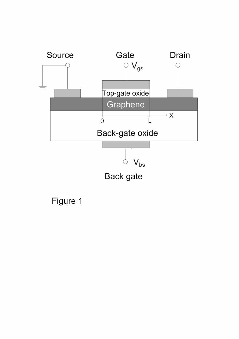
dual gate GFET with the cross-section depicted in Fig. 1. It consists of a graphene sheet
playing the role of the active channel. The source and drain electrodes are contacting the
graphene channel and are assumed to be ohmic. The electrostatic modulation of the
carrier concentration in graphene is achieved via a double-gate stack consisting of top and
bottom gate dielectric and the corresponding metal gate. The source is grounded and
considered the reference potential in the device.
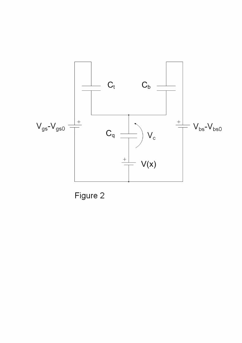
The electrostatics of this device can be understood using the equivalent capacitive circuit
depicted in Fig. 2 (see Ref. [10]). Here, Ct and Cb are the top and bottom oxide
capacitances and Cq represents the quantum capacitance of the graphene. The potential
Vc represents the voltage drop across Cq, and the relation between them is given by
| |, where F
and vF (=106 m/s) is the Fermi velocity [12]. This expression
is valid under the condition qVc>>kBT. The potential V(x) is the voltage drop in the
graphene channel, which is zero at the source end (x=0) and equal to the drain-source
voltage (Vds) at the drain end (x=L). Applying basic circuit laws to the equivalent capacitive
network and noting that the overall net mobile sheet charge density in the graphene
channel, defined as Qc=q(p-n), is equal to -(1/2)CqVc, the following relation can be
obtained:
12
12
1
where Vgs-Vgs0 and Vbs-Vbs0 are the top and back gate-source voltage overdrive,
respectively. These quantities comprise work-function differences between the gates and
the graphene channel, eventual charged interface states at the graphene/oxide interfaces,
and intentional or unintentional doping of the graphene.
To model the drain current of the GFET a drift-diffusion transport is assumed under the
form Ids=-W|Qc(x)|v(x), where W is the gate width, |Qc| is the free carrier sheet density in
the channel at position x, and v(x) the carrier drift velocity. The absolute value of Qc is
taken because negative charged electrons and positive charged holes move in opposite
directions under the electric field action, additively contributing to the drain-current. Using a
soft-saturation model, consistent with Monte Carlo simulations [13], v(x) can be expressed
as v=E/(1+|E|/vsat), where E is the electric field, is the carrier low-field mobility, and vsat
is the saturation velocity. We assume that the saturation velocity is pinned to the Fermi
velocity (vsat=vF), greatly simplifying the algebra. A more refined model, relating the
saturation velocity with the carrier density, could be considered instead [9]. Applying E=-
dV(x)/dx, combining the above expressions for v and vsat, and integrating the resulting
equation over the device length, the drain current becomes:
| |
| | 2
The denominator represents an effective length (Leff) that takes into account the saturation
velocity effect. In order to get an explicit expression for the drain current, the integral in Eq.
(2) is solved using Vc as the integration variable and consistently expressing Qc as a
function of Vc :
| |
| | 3
Here Vc is obtained from Eq. (1) and can be written as:
2 4
where the positive (negative) sign applies when
0 0 . The channel potential at the source (Vcs) is determined as Vc(V=0). Similarly, the
channel potential at the drain (Vcd) is determined as Vc(V=Vds). Moreover, Eq. (1) provides
the relation 1 entering in Eq. (3), where sgn refers to the sign
function. On the other hand, the charge sheet density can be written as | | 2⁄ .
Inserting these expressions into Eq. (3), the following explicit drain current expression can
be finally obtained:
2
3 4
| | (5)
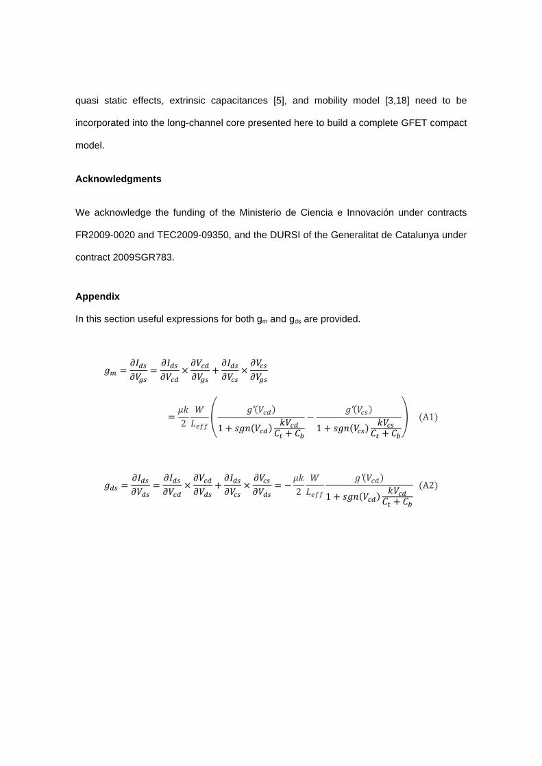
Useful expressions for both the transconductance ( and output conductance
( are given in the Appendix.
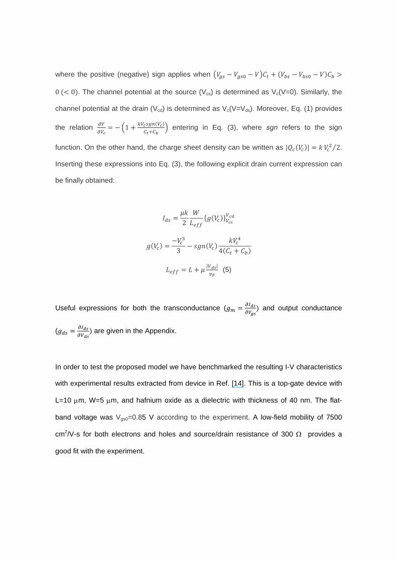
In order to test the proposed model we have benchmarked the resulting I-V characteristics
with experimental results extracted from device in Ref. [14]. This is a top-gate device with
L=10 m, W=5 m, and hafnium oxide as a dielectric with thickness of 40 nm. The flat-
band voltage was Vgs0=0.85 V according to the experiment. A low-field mobility of 7500
cm2/V-s for both electrons and holes and source/drain resistance of 300 provides a
good fit with the experiment.
To reproduce any experimental current-voltage characteristics of GFETs, accounting of
the voltage drop at the source/drain contacts is necessary. This quantity must be removed
from the external applied bias (Vds_ext) in order to get the internal Vds. This is simply done
by solving the equation Vds = Vds_ext-Ids(Vds)(Rs+Rd), where Rs and Rd represents the source
and drain contact resistance, respectively. Finally note that Ids is a function of Vds as given
by Eq. (5).
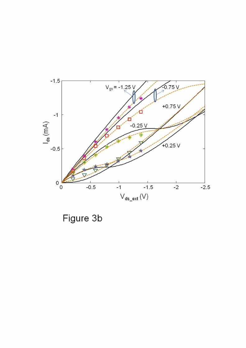
The resulting I-V characteristics are shown in Fig. 3. We have extended the analyzed
drain-source voltage range beyond the experiment to show the predictive behavior of the
model. The transfer characteristics exhibit the expected ambipolar behavior dominated by
holes (electrons) below and above the Dirac gate voltage. The output characteristics show
a saturation-like behavior with a second linear region. The agreement between the
proposed model (solid lines) and the experiment (symbols) demonstrates its accuracy. A
closer agreement can even be obtained using a more refined model given in Ref. [9]
(dashed lines).
Charge model
In this section we provide analytical and continuous expressions of charges associated
with each terminal. We consider the important case of a double-gate configuration, where
the two gates are connected together. This allows considering the GFET as a 3-terminal
device, therefore making the analysis simpler. Extension to 4-terminal devices could be
done using the same principles outlined in this work.
The terminal charges Qg, Qd, and Qs, associated with the gate, drain and source
electrodes have to be considered. The gate charge can be computed by integrating the net
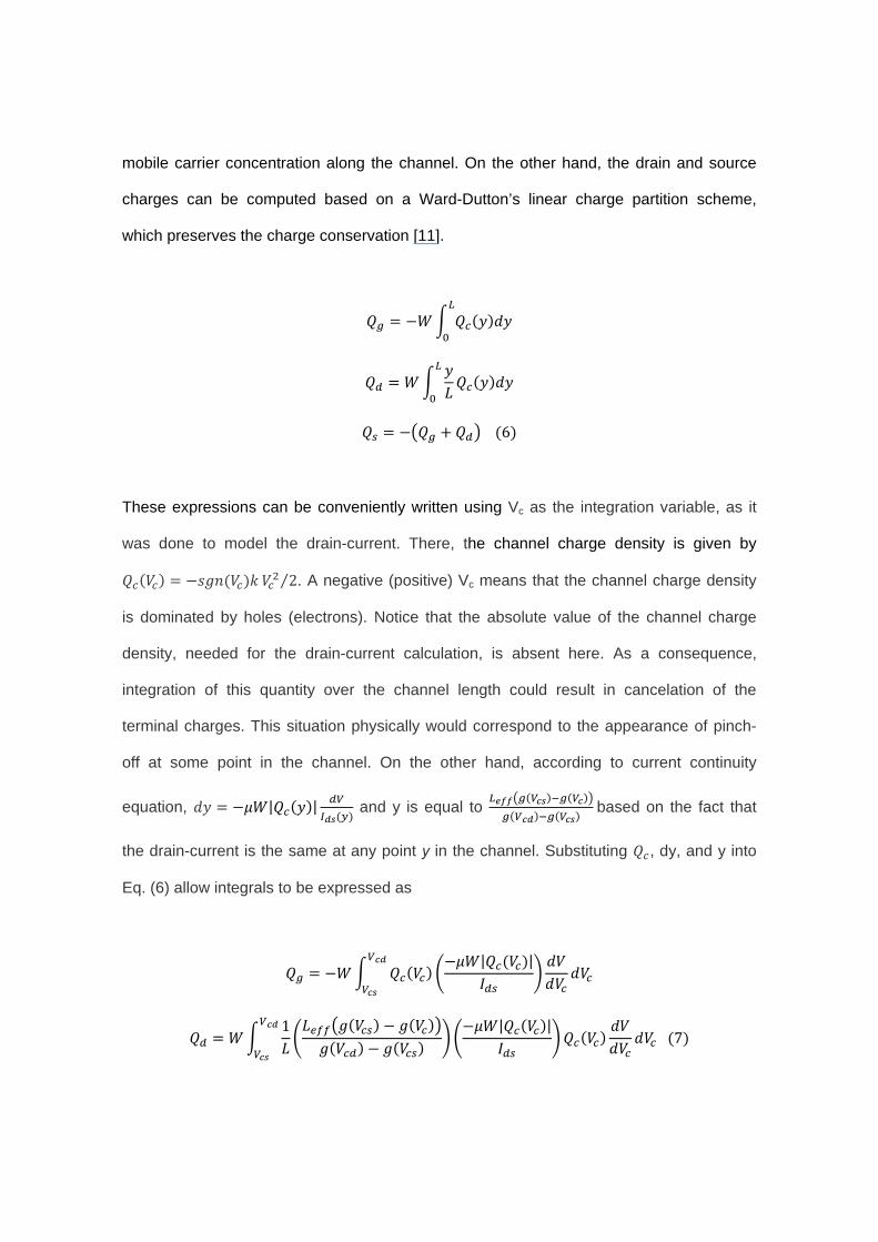
mobile carrier concentration along the channel. On the other hand, the drain and source
charges can be computed based on a Ward-Dutton’s linear charge partition scheme,
which preserves the charge conservation [11].
6
These expressions can be conveniently written using Vc as the integration variable, as it
was done to model the drain-current. There, the channel charge density is given by
2⁄ . A negative (positive) Vc means that the channel charge density
is dominated by holes (electrons). Notice that the absolute value of the channel charge
density, needed for the drain-current calculation, is absent here. As a consequence,
integration of this quantity over the channel length could result in cancelation of the
terminal charges. This situation physically would correspond to the appearance of pinch-
off at some point in the channel. On the other hand, according to current continuity
equation, | | and y is equal to based on the fact that
the drain-current is the same at any point y in the channel. Substituting , dy, and y into
Eq. (6) allow integrals to be expressed as
| |
1 | | 7
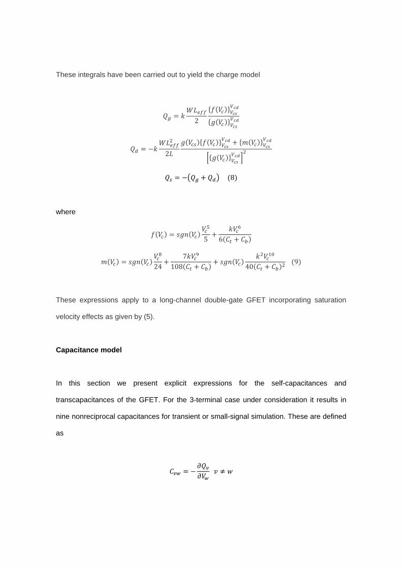
These integrals have been carried out to yield the charge model
2
2
8
where
5 6
247
108 40 9
These expressions apply to a long-channel double-gate GFET incorporating saturation
velocity effects as given by (5).
Capacitance model
In this section we present explicit expressions for the self-capacitances and
transcapacitances of the GFET. For the 3-terminal case under consideration it results in
nine nonreciprocal capacitances for transient or small-signal simulation. These are defined
as
10
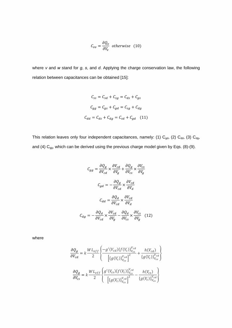
where v and w stand for g, s, and d. Applying the charge conservation law, the following
relation between capacitances can be obtained [15]:
11
This relation leaves only four independent capacitances, namely: (1) Cgd, (2) Cdd, (3) Cdg,
and (4) Cgg, which can be derived using the previous charge model given by Eqs. (8)-(9).
12
where
2
2
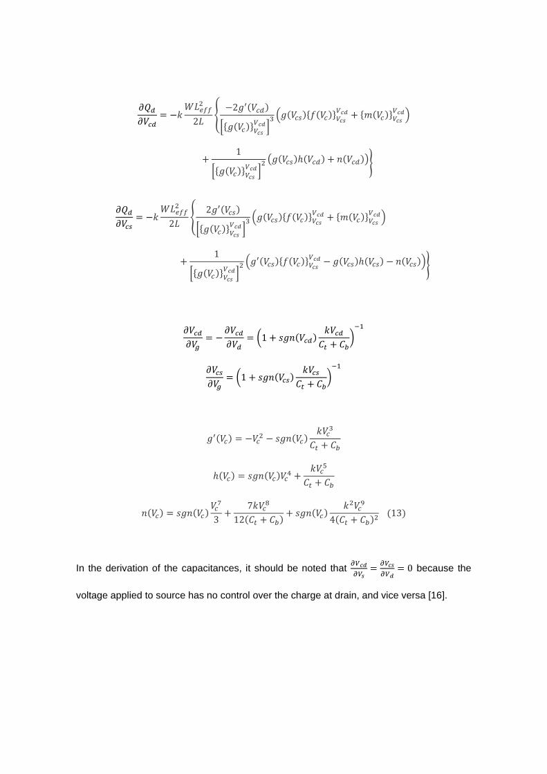
22
1
22
1
1
1
37
12 4 13
In the derivation of the capacitances, it should be noted that 0 because the
voltage applied to source has no control over the charge at drain, and vice versa [16].
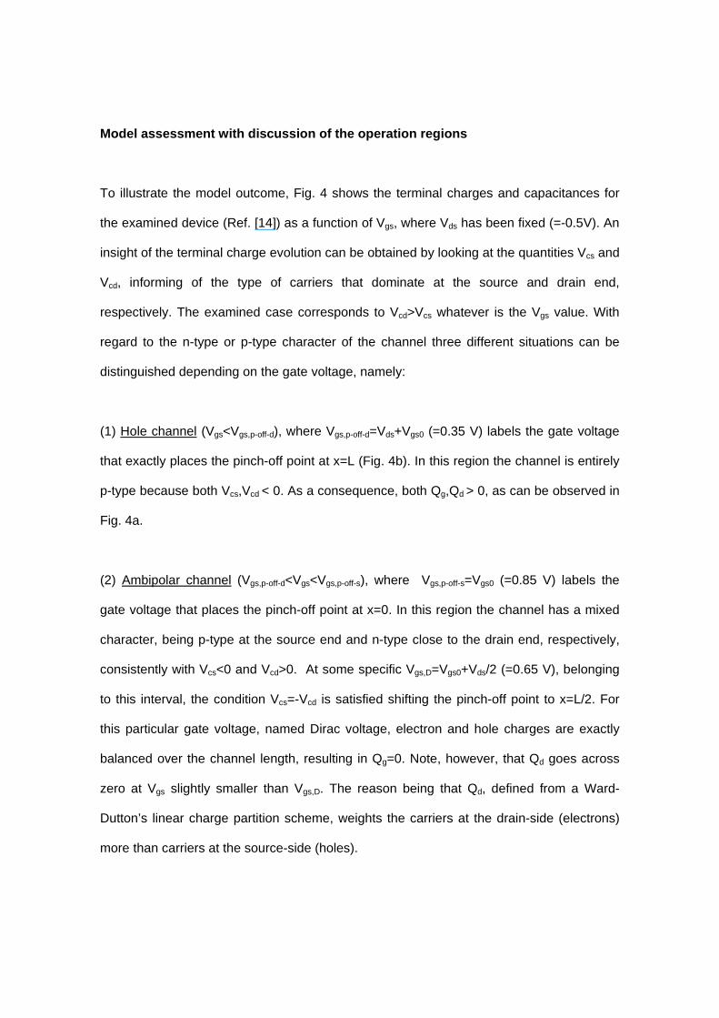
Model assessment with discussion of the operation regions
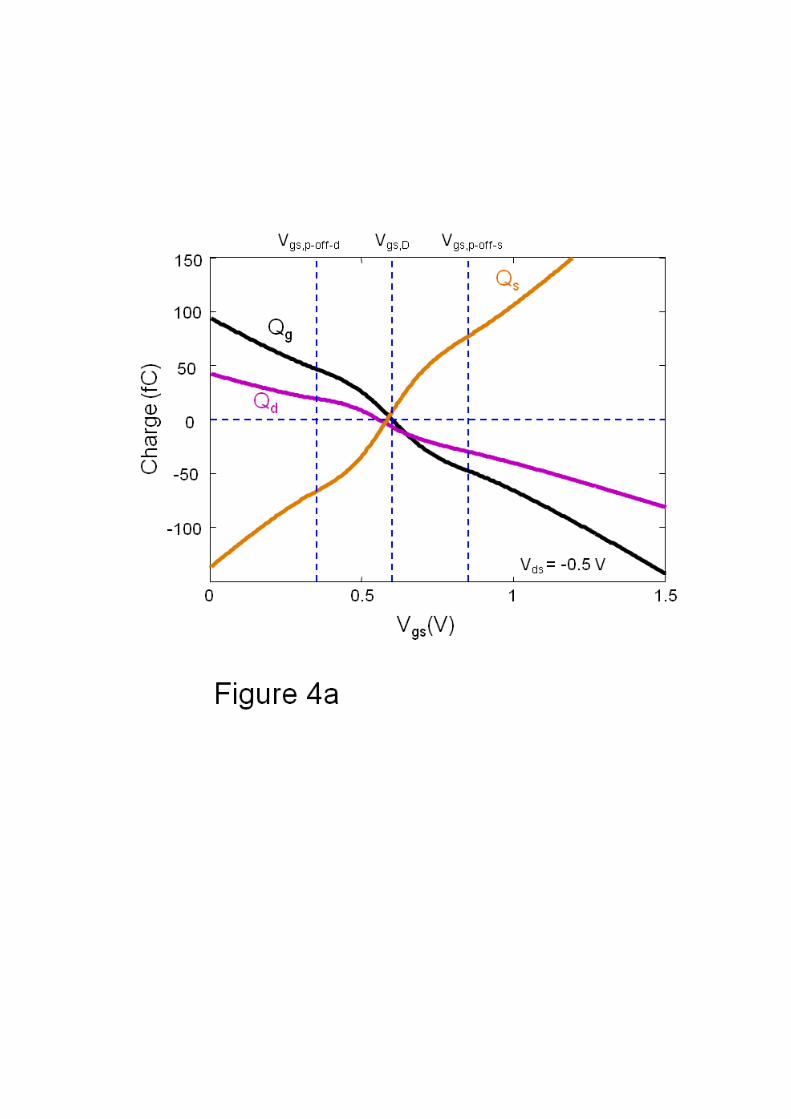
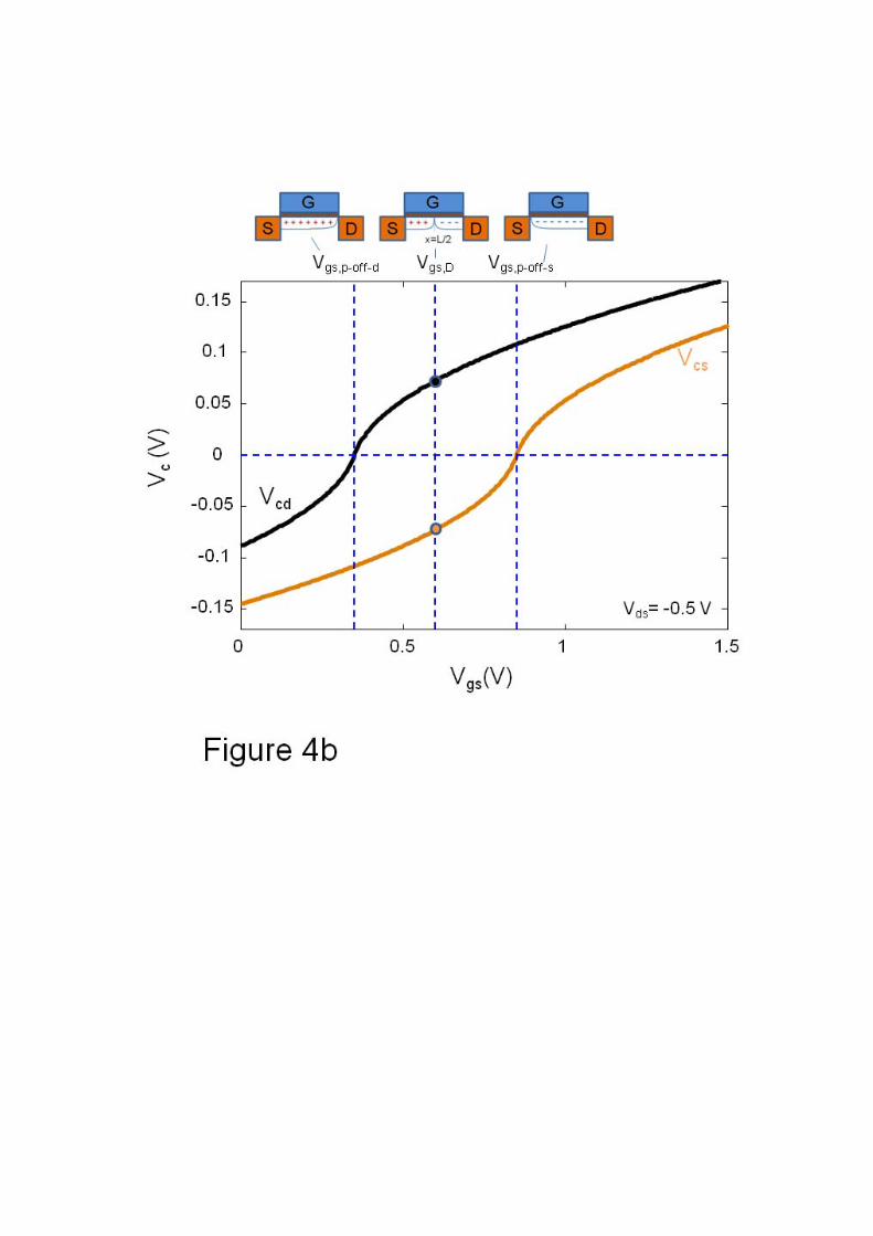
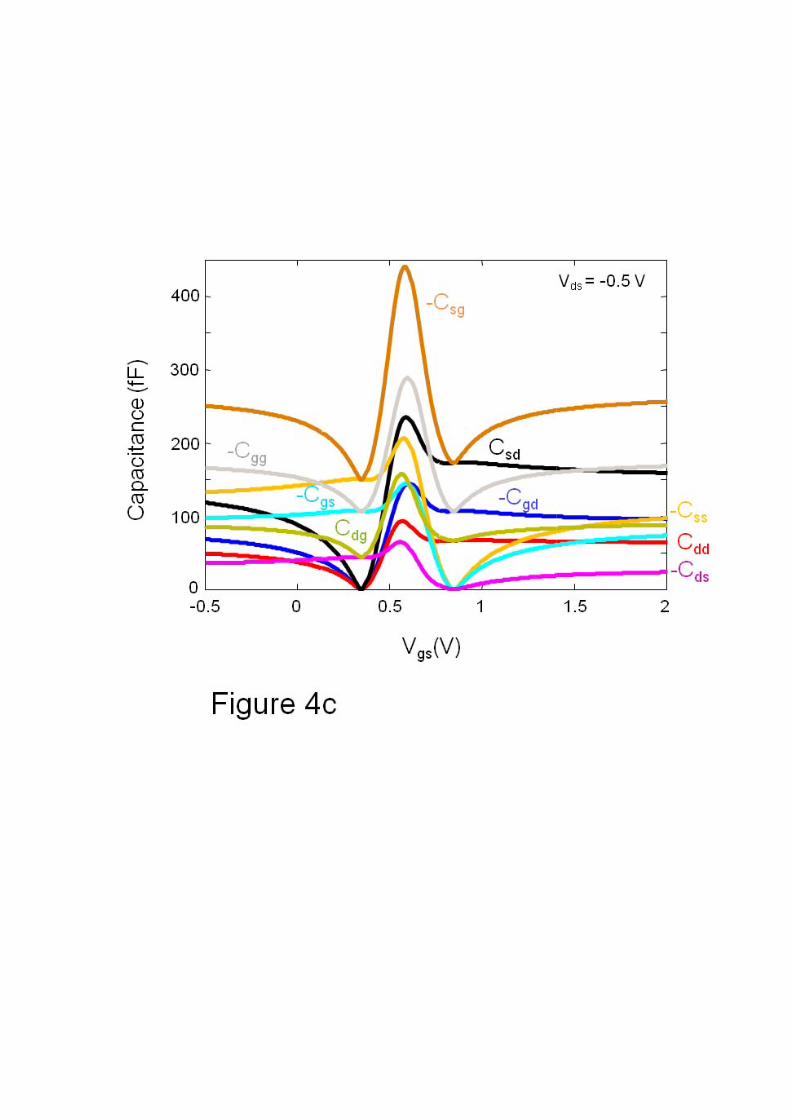
To illustrate the model outcome, Fig. 4 shows the terminal charges and capacitances for
the examined device (Ref. [14]) as a function of Vgs, where Vds has been fixed (=-0.5V). An
insight of the terminal charge evolution can be obtained by looking at the quantities Vcs and
Vcd, informing of the type of carriers that dominate at the source and drain end,
respectively. The examined case corresponds to Vcd>Vcs whatever is the Vgs value. With
regard to the n-type or p-type character of the channel three different situations can be
distinguished depending on the gate voltage, namely:
(1) Hole channel (Vgs<Vgs,p-off-d), where Vgs,p-off-d=Vds+Vgs0 (=0.35 V) labels the gate voltage
that exactly places the pinch-off point at x=L (Fig. 4b). In this region the channel is entirely
p-type because both Vcs,Vcd < 0. As a consequence, both Qg,Qd > 0, as can be observed in
Fig. 4a.
(2) Ambipolar channel (Vgs,p-off-d<Vgs<Vgs,p-off-s), where Vgs,p-off-s=Vgs0 (=0.85 V) labels the
gate voltage that places the pinch-off point at x=0. In this region the channel has a mixed
character, being p-type at the source end and n-type close to the drain end, respectively,
consistently with Vcs<0 and Vcd>0. At some specific Vgs,D=Vgs0+Vds/2 (=0.65 V), belonging
to this interval, the condition Vcs=-Vcd is satisfied shifting the pinch-off point to x=L/2. For
this particular gate voltage, named Dirac voltage, electron and hole charges are exactly
balanced over the channel length, resulting in Qg=0. Note, however, that Qd goes across
zero at Vgs slightly smaller than Vgs,D. The reason being that Qd, defined from a Ward-
Dutton’s linear charge partition scheme, weights the carriers at the drain-side (electrons)
more than carriers at the source-side (holes).
(3) Electron channel (Vgs>Vgs,p-off-s). In this region the channel is entirely n-type because
both Vcs,Vcd > 0, consistently with the quantities Qg,Qd < 0.
It is worth noting that if the selected Vds results in Vcs >Vcd the operation regions would be
instead: (1) Hole channel (Vgs<Vgs,p-off-s), (2) Ambipolar channel (Vgs,p-off-s<Vgs<Vgs,p-off-d), (3)
Electron channel (Vgs>Vgs,p-off-d).
Next I examine the capacitances of the GFET under test (Fig. 4c). Interestingly, the self-
capacitance -Cgg is symmetric around the Dirac voltage, where a maximum value arises. It
also presents two local minimum at Vgs,p-off-d and Vgs,p-off-s, respectively. The
transcapacitances -Csg and Cdg show a similar behavior, although the curves are slightly
asymmetric due to the position-dependent weighting of the mobile charge in the Ward-
Dutton’s partition scheme. Moreover, the position of the maximum is slightly shifted
respect to the Dirac voltage. On the other hand, the capacitances Csd, -Cgd, Cdd (-Css, -Cgs,
-Cds) exhibit a zero value at Vgs,p-off-d (Vgs,p-off-s) and a maximum around Vgs,D.
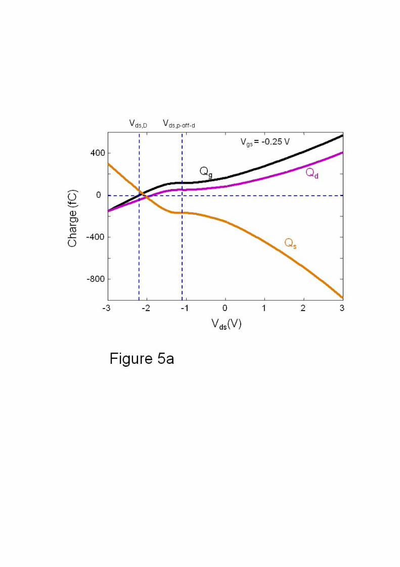
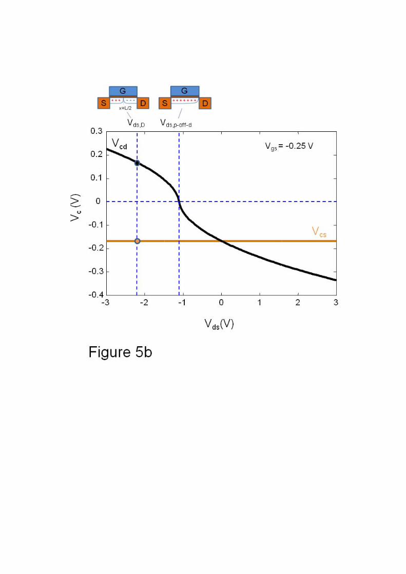
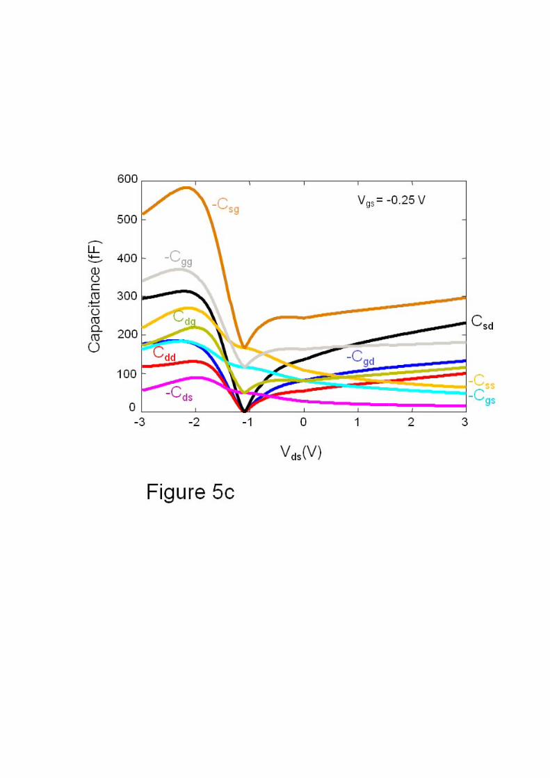
Next, we examine the terminal charges and capacitances as a function of Vds for a fixed
Vgs (=-0.25 V) (see Fig. 5). In this case Vcs is constant (<0) and different operation regions
appear driven by Vcd. Two different channel types are then possible according to the drain
voltage, namely:
(1) Ambipolar channel (Vds<Vds,p-off-d), where Vds,p-off-d=Vgs-Vgs0 (=-1.1V) labels the drain
voltage that places the pinch-off point at x=L. In this region the channel has a mixed p-type
and n-type character at the source and drain end, respectively, consistently with Vcs <0 and
Vcd >0. On the other hand, Qg<0 as long as Vds<Vds,D, where Vds,D = 2 Vds,p-off-d (=-2.2 V) is
the drain voltage that places the pinch-off just in the middle of the channel (x=L/2), where

the relation Vcs=-Vcd is fulfilled. Regarding the drain-current, this is roughly linear with Vds.
This region is named as second linear region. As long as Vds approaches Vds,p-off-d the
output characteristics get saturated. This behavior can be observed in the GFET output
characteristics of the device under test in Fig. 3b. Note that Vds_ext has been considered as
the independent variable for plotting this figure, being different from Vds; the later meaning
the internal drain-source voltage.
(2) Hole channel (Vds>Vds,p-off-d). In this region the channel is entirely p-type, consistently
with Vcs,Vcd <0 and Qg,Qd >0. For this particular range of Vds, the output characteristic is
linear with Vds and it is named as first linear region.
It is worth noting that if the selected Vgs results in Vcs>0 the operation regions would be
instead: (1) Electron channel (Vds<Vds,p-off-d), (2) Ambipolar channel (Vds>Vgs,p-off-d).
The capacitances Csd, -Cgd, and Cdd as a function of Vds show a maximum around Vds,D and
a minimum zero capacitance at Vds,p-off-d, where all the terminal charges Qs, Qg, and Qd get
saturated (Figs. 5b and 5c).
Conclusion
In conclusion, I have presented an explicit and compact drain current, charge and
capacitance model for GFETs based on a field-effect model and drift-diffusion carrier
transport, including saturation velocity effects. The model captures the physics of all
operation regions within a single expression for the drain current and each terminal charge
and capacitance. It is of especial interest as a tool for design of analog and RF
applications [17]. Additional physical effects as, for example, short-channel effects, non-
quasi static effects, extrinsic capacitances [5], and mobility model [3,18] need to be
incorporated into the long-channel core presented here to build a complete GFET compact
model.
Acknowledgments We acknowledge the funding of the Ministerio de Ciencia e Innovación under contracts
FR2009-0020 and TEC2009-09350, and the DURSI of the Generalitat de Catalunya under
contract 2009SGR783.
Appendix
In this section useful expressions for both gm and gds are provided.
2′
1
′
1 A1
2′
1 A2
References
[1] Y. Wu, Y-M. Lin, A. A. Bol, K. A. Jenkins, F. Xia, D. B. Farmer, Y. Zhu, and P. Avouris,
“High-frequency, scaled graphene transistors on diamond-like carbon”, Nature 472, pp. 74-
78 (2011).
[2] F. Schwierz, “Graphene transistors”, Nature Nanotechnology, vol. 5, pp. 487-496
(2010).
[3] I. Meric, M. Y. Han, A. F. Young, B. Ozyilmaz, P. Kim, and K. Shepard, “Current
saturation in zero-bandgap, top-gated graphene field-effect transistors”, Nature
Nanotechnology, vol. 3, pp. 654-659, (2008)
[4] J. Bai, L. Liao, H. Zhou, R. Cheng, L. Liu, Y. Huang, and X. Duan, “Top gated chemical
vapor deposition grown graphene transistors with current saturation”, Nano Lett.,
DOI: 10.1021/nl201331x (2011).
[5] S. O. Koswatta, A. Valdes-Garcia, M. B. Steiner, Y-M. Lin, and P. Avouris, “Ultimate RF
performance potential of carbon electronics”, arXiv: 1105.1060
[6] Y.-M. Lin, C. Dimitrakopoulos, K. A. Jenkins, D. B. farmer, H.-Y. Chiu, A. Grill, and Ph.
Avouris, “100-GHz transistors from wafer-scale epitaxial graphene”, Science 327, no.
5966, p. 662 (2010)
[7] L. Liao, Y-C. Lin, M. Bao, R Cheng, J. Bai, Y. Liu, Y. Qu, K. L. Wang, Y. Huan, and X.
Duan, “High-speed graphene transistors with a self-aligned nanowire gate ”, Nature 467,
no. 16, pp. 305-308 (2010).
[8] D. Jiménez, “A current-voltage model for Schottky-barrier graphene based transistors,”
Nanotechnology, vol. 19, 345204 (2008).
[9] D. Jiménez and O. Moldovan, “Explicit drain-current model of graphene field-effect
transistors targeting analog and radio-frequency applications”, arXiv: 1103.1599
[10] S. Thiele, J. A. Schaefer, and F. Schwierz, “Modeling of graphene metal-oxide-
semiconductor field-effect transistors with gapless large-area graphene channels”, Journal
of Applied Physics, vol. 107, 094505 (2010).
[11] D. Ward and R. Dutton, “A charge-oriented model for MOS transistor capacitances,”
IEEE J. Solid State Circuits, vol. SSC-13, no. 5, pp. 703-708, Oct. 1978.
[12] T. Fang, A. Konar, H. Xing, and D. Jena, “Carrier statistics and quantum capacitance
of graphene sheets and ribbons,” Appl. Phys. Lett., vol. 91, 092109 (2007).
[13] J. Chauhan and J. Guo, “High-field transport and velocity saturation in graphene,”
Appl. Phys. Lett., vol. 95, 023120 (2009).
[14] J. Kedzierski, P-L. Hsu, A. Reina, J. Kong, P. Healey, P. Wyatt, and C. Keast,
“Graphene-on-insulator transistors made using C on Ni chemical-vapor deposition,” IEEE
Electron Device Lett., vol. 30, pp. 745-747, (2009).
[15] H. Lu and Y. Taur, “An analytic potential model for symmetric and asymmetrid DG
MOSFETs,” IEEE Trans. Electron Devices, vol. 53, no. 5, May 2006.
[16] F. Liu, J. Zhang, F. He, F. Liu, L. Zhang, and M. Chan, “A charge-based compact
model for predicting the current-voltage and capacitance-voltage characteristics of heavily
doped cylindrical surrounding-gate MOSFETs,” Solid-State Electronics, vol. 53, pp. 49-53
(2009).
[17] D. Jiménez, B. Iñíguez, J. Suñé, J. J. Sáenz, “Analog performance of the nanoscale
double-gate metal-oxide-semiconductor field-effect-transistor near the ultimate scaling
limits,” J. Appl. Phys., vol. 96, no. 9, pp. 5271-5276 (2003).
[18] V. E. Dorgan, M-H Bae, and E. Pop, “Mobility and saturation velocity in graphene on
SiO2,” Appl. Phys. Lett. 97, 082112 (2010).
Figure captions:
Fig. 1. Cross section of the dual-gate GFET.
Fig. 2. Equivalent capacitive circuit of the dual-gate GFET.
Fig. 3. Transfer (a) and output (b) characteristics obtained from the analytical model (solid
lines) compared with experimental results from Ref. [14] (symbols) and a more elaborated
analytical model (dashed lines), which incorporates the effect of doping and a saturation
velocity model that takes into account the carrier density (see Ref. [9]) .
Fig. 4. Terminal charges (a), channel voltage drop (b), and capacitances (c) for the
examined device, as a function of the gate voltage. The channel is shown to be p-type,
mixed p and n-type, or p-type, depending on the gate voltage.
Fig. 5. Terminal charges (a), channel voltage drop (b), and capacitances (c) for the
examined device, as a function of the drain voltage. The channel is shown to be mixed p
and n type, or p-type, depending on the drain voltage.


Related Documents


