Experimental and simulated study of electrical behaviour of ZnO film deposited on Al substrate for device applications Priyabrata Pattanaik • Sushanta Kumar Kamilla • Debi Prasad Das • Dilip Kumar Mishra Received: 15 February 2014 / Accepted: 3 May 2014 / Published online: 10 May 2014 Ó Springer Science+Business Media New York 2014 Abstract In this paper, zinc oxide (ZnO) film has been deposited on Al substrate by chemical wet and dry tech- nique which is just a simple modified version of the dip coating method. In this method, it is possible to precisely control the immersion and withdrawal speed, with drying as well as annealing at the same time. The polycrystalline nature of ZnO has been confirmed by X-ray diffraction (XRD) analysis. The XRD analysis clearly indicates that some percentage of Al diffuses into the ZnO matrix at its interface region; hence it affects mobility of the sample. Hall measurement indicates the ZnO semiconductor as n-type. I–V characteristic of the sample shows that the contact is Ohmic and it can be used as a sensor at low potential value. The mobility decreases with increase in temperature. The simulation study carried out for I–V and mobility through simulation using ATLAS (SILVACO) software confirms that the experimental and simulation results are in close agreement with respect to the I–V characteristic and the mobility. 1 Introduction There has been an extensive study on zinc oxide (ZnO) in recent years due to its potential application in the area of spintronics, magneto-electronics and optoelectronics [1–7]. Especially, ZnO is a very promising material for the fabri- cation of semiconductor devices as it is a wide and direct band gap semiconductor. A wide band gap semiconductor has many benefits for high temperature and power operations, reducing electronic noise, making sustenance in large electric fields possible and raising breakdown voltages [8–10]. These features make this material attractive for various applications in power electronics devices, solar cells, semiconductor gas sensors, optical coating UV semiconductor lasers, spintronics devices and photocatalytic activities etc. Looking into all above applications, ZnO films have been grown by several techniques such as metal–organic chemical vapour deposition (MOCVD) [11], chemical vapour deposition (CVD) [12], RF magnetron sputtering [13], DC magnetron sputtering [14] and pulsed laser deposition (PLD) [15]. The most advantage feature in ZnO is that it can be grown easily by any techniques. Hence, it is possible to choose a suitable low cost technology for the fabrication of ZnO devices. In consideration to the low cost technology, ZnO film is preferred to be grown by different chemical tech- niques like sol gel spin and dip coating techniques, which are versatile and low cost system to prepare ZnO film [16, 17]. Particularly, the sol–gel processes are well adapted to pro- duce ZnO films in a simple and highly controlled way. A number of reports highlighted the sol–gel synthesis of undoped homogeneous ZnO films on different substrate for various applications including the chemical and physical parameters influencing their structural properties [18, 19]. The optical and electrical properties of group III metals (Al, Ga, In) doped in ZnO film prepared by sol–gel process was reported [20]. However, a few works on ZnO film on Al substrate have been reported till date [21–23]. The re- view of electron mobilities, and corresponding carrier con- centration obtained in nominally undoped bulk and thin-film ZnO deposited on different substrates by various growth P. Pattanaik Á S. K. Kamilla Á D. K. Mishra (&) Semiconductors Research Laboratory, Institute of Technical Education and Research, Siksha ‘O’ Anusandhan University, Khandagiri Square, Bhubaneswar 751030, Odisha, India e-mail: [email protected] D. P. Das CSIR-Institute of Minerals and Materials Technology, Bhubaneswar 751013, Odisha, India 123 J Mater Sci: Mater Electron (2014) 25:3062–3068 DOI 10.1007/s10854-014-1984-1

Welcome message from author
This document is posted to help you gain knowledge. Please leave a comment to let me know what you think about it! Share it to your friends and learn new things together.
Transcript
Experimental and simulated study of electrical behaviour of ZnOfilm deposited on Al substrate for device applications
Priyabrata Pattanaik • Sushanta Kumar Kamilla •
Debi Prasad Das • Dilip Kumar Mishra
Received: 15 February 2014 / Accepted: 3 May 2014 / Published online: 10 May 2014
� Springer Science+Business Media New York 2014
Abstract In this paper, zinc oxide (ZnO) film has been
deposited on Al substrate by chemical wet and dry tech-
nique which is just a simple modified version of the dip
coating method. In this method, it is possible to precisely
control the immersion and withdrawal speed, with drying
as well as annealing at the same time. The polycrystalline
nature of ZnO has been confirmed by X-ray diffraction
(XRD) analysis. The XRD analysis clearly indicates that
some percentage of Al diffuses into the ZnO matrix at its
interface region; hence it affects mobility of the sample.
Hall measurement indicates the ZnO semiconductor as
n-type. I–V characteristic of the sample shows that the
contact is Ohmic and it can be used as a sensor at low
potential value. The mobility decreases with increase in
temperature. The simulation study carried out for I–V and
mobility through simulation using ATLAS (SILVACO)
software confirms that the experimental and simulation
results are in close agreement with respect to the I–V
characteristic and the mobility.
1 Introduction
There has been an extensive study on zinc oxide (ZnO) in
recent years due to its potential application in the area of
spintronics, magneto-electronics and optoelectronics [1–7].
Especially, ZnO is a very promising material for the fabri-
cation of semiconductor devices as it is a wide and direct band
gap semiconductor. A wide band gap semiconductor has
many benefits for high temperature and power operations,
reducing electronic noise, making sustenance in large electric
fields possible and raising breakdown voltages [8–10]. These
features make this material attractive for various applications
in power electronics devices, solar cells, semiconductor gas
sensors, optical coating UV semiconductor lasers, spintronics
devices and photocatalytic activities etc. Looking into all
above applications, ZnO films have been grown by several
techniques such as metal–organic chemical vapour deposition
(MOCVD) [11], chemical vapour deposition (CVD) [12], RF
magnetron sputtering [13], DC magnetron sputtering [14] and
pulsed laser deposition (PLD) [15].
The most advantage feature in ZnO is that it can be grown
easily by any techniques. Hence, it is possible to choose a
suitable low cost technology for the fabrication of ZnO
devices. In consideration to the low cost technology, ZnO
film is preferred to be grown by different chemical tech-
niques like sol gel spin and dip coating techniques, which are
versatile and low cost system to prepare ZnO film [16, 17].
Particularly, the sol–gel processes are well adapted to pro-
duce ZnO films in a simple and highly controlled way. A
number of reports highlighted the sol–gel synthesis of
undoped homogeneous ZnO films on different substrate for
various applications including the chemical and physical
parameters influencing their structural properties [18, 19].
The optical and electrical properties of group III metals (Al,
Ga, In) doped in ZnO film prepared by sol–gel process was
reported [20]. However, a few works on ZnO film on Al
substrate have been reported till date [21–23]. The re-
view of electron mobilities, and corresponding carrier con-
centration obtained in nominally undoped bulk and thin-film
ZnO deposited on different substrates by various growth
P. Pattanaik � S. K. Kamilla � D. K. Mishra (&)
Semiconductors Research Laboratory, Institute of Technical
Education and Research, Siksha ‘O’ Anusandhan University,
Khandagiri Square, Bhubaneswar 751030, Odisha, India
e-mail: [email protected]
D. P. Das
CSIR-Institute of Minerals and Materials Technology,
Bhubaneswar 751013, Odisha, India
123
J Mater Sci: Mater Electron (2014) 25:3062–3068
DOI 10.1007/s10854-014-1984-1
techniques was reported earlier. However, no much study on
electrical behaviour, electron mobility and corresponding
carrier concentrations have been carried out on ZnO film
deposited over Al substrate.
Hence, in this study, a uniform thickness of ZnO film is
deposited on Al substrate using the sol–gel and a newly
developed modified chemically wet and dry (CWD) method.
The electrical characterizations of the film were done by
using four probe method and Hall Effect measurement with
the help of data acquisition system (NI PXI-1042) and data
acquisition card NI PXI-4072 including related software.
Experimentally investigated temperature-dependent carrier
mobility and concentration were used to determine the
fundamental material parameters and understand the carrier
scattering mechanism along with an accurate comparison
with theory. In addition to this, these experimentally
obtained physical parameters were optimized by device
simulation software, the Technology Computer Aided
Design (TCAD; Make: ATLAS, SILVACO). It is intended
to determine the optimum condition that would lead to the
manufacturing of well crystallized, semi-conductive and
transparent ZnO films on Al substrate for device fabrication.
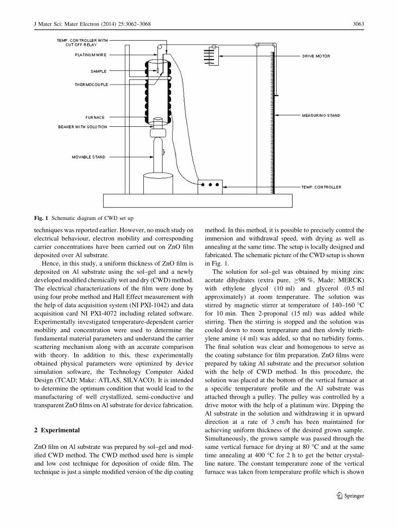
2 Experimental
ZnO film on Al substrate was prepared by sol–gel and mod-
ified CWD method. The CWD method used here is simple
and low cost technique for deposition of oxide film. The
technique is just a simple modified version of the dip coating
method. In this method, it is possible to precisely control the
immersion and withdrawal speed, with drying as well as
annealing at the same time. The setup is locally designed and
fabricated. The schematic picture of the CWD setup is shown
in Fig. 1.
The solution for sol–gel was obtained by mixing zinc
acetate dihydrates (extra pure, C98 %, Made: MERCK)
with ethylene glycol (10 ml) and glycerol (0.5 ml
approximately) at room temperature. The solution was
stirred by magnetic stirrer at temperature of 140–160 �C
for 10 min. Then 2-proponal (15 ml) was added while
stirring. Then the stirring is stopped and the solution was
cooled down to room temperature and then slowly trieth-
ylene amine (4 ml) was added, so that no turbidity forms.
The final solution was clear and homogenous to serve as
the coating substance for film preparation. ZnO films were
prepared by taking Al substrate and the precursor solution
with the help of CWD method. In this procedure, the
solution was placed at the bottom of the vertical furnace at
a specific temperature profile and the Al substrate was
attached through a pulley. The pulley was controlled by a
drive motor with the help of a platinum wire. Dipping the
Al substrate in the solution and withdrawing it in upward
direction at a rate of 3 cm/h has been maintained for
achieving uniform thickness of the desired grown sample.
Simultaneously, the grown sample was passed through the
same vertical furnace for drying at 80 �C and at the same
time annealing at 400 �C for 2 h to get the better crystal-
line nature. The constant temperature zone of the vertical
furnace was taken from temperature profile which is shown
Fig. 1 Schematic diagram of CWD set up
J Mater Sci: Mater Electron (2014) 25:3062–3068 3063
123
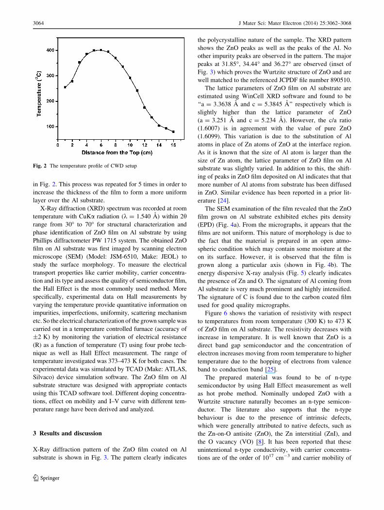
in Fig. 2. This process was repeated for 5 times in order to
increase the thickness of the film to form a more uniform
layer over the Al substrate.
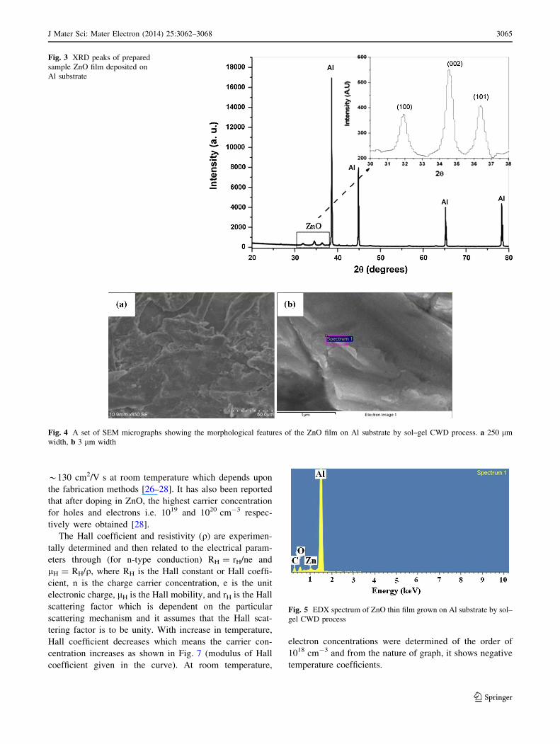
X-Ray diffraction (XRD) spectrum was recorded at room
temperature with CuKa radiation (k = 1.540 A) within 2hrange from 30� to 70� for structural characterization and
phase identification of ZnO film on Al substrate by using
Phillips diffractometer PW 1715 system. The obtained ZnO
film on Al substrate was first imaged by scanning electron
microscope (SEM) (Model: JSM-6510, Make: JEOL) to
study the surface morphology. To measure the electrical
transport properties like carrier mobility, carrier concentra-
tion and its type and assess the quality of semiconductor film,
the Hall Effect is the most commonly used method. More
specifically, experimental data on Hall measurements by
varying the temperature provide quantitative information on
impurities, imperfections, uniformity, scattering mechanism
etc. So the electrical characterization of the grown sample was
carried out in a temperature controlled furnace (accuracy of
±2 K) by monitoring the variation of electrical resistance
(R) as a function of temperature (T) using four probe tech-
nique as well as Hall Effect measurement. The range of
temperature investigated was 373–473 K for both cases. The
experimental data was simulated by TCAD (Make: ATLAS,
Silvaco) device simulation software. The ZnO film on Al
substrate structure was designed with appropriate contacts
using this TCAD software tool. Different doping concentra-
tions, effect on mobility and I–V curve with different tem-
perature range have been derived and analyzed.
3 Results and discussion
X-Ray diffraction pattern of the ZnO film coated on Al
substrate is shown in Fig. 3. The pattern clearly indicates
the polycrystalline nature of the sample. The XRD pattern
shows the ZnO peaks as well as the peaks of the Al. No
other impurity peaks are observed in the pattern. The major
peaks at 31.85�, 34.44� and 36.27� are observed (inset of
Fig. 3) which proves the Wurtzite structure of ZnO and are
well matched to the referenced JCPDF file number 890510.
The lattice parameters of ZnO film on Al substrate are
estimated using WinCell XRD software and found to be
‘‘a = 3.3638 A and c = 5.3845 A’’ respectively which is
slightly higher than the lattice parameter of ZnO
(a = 3.251 A and c = 5.234 A). However, the c/a ratio
(1.6007) is in agreement with the value of pure ZnO
(1.6099). This variation is due to the substitution of Al
atoms in place of Zn atoms of ZnO at the interface region.
As it is known that the size of Al atom is larger than the
size of Zn atom, the lattice parameter of ZnO film on Al
substrate was slightly varied. In addition to this, the shift-
ing of peaks in ZnO film deposited on Al indicates that that
more number of Al atoms from substrate has been diffused
in ZnO. Similar evidence has been reported in a prior lit-
erature [24].
The SEM examination of the film revealed that the ZnO
film grown on Al substrate exhibited etches pits density
(EPD) (Fig. 4a). From the micrographs, it appears that the
films are not uniform. This nature of morphology is due to
the fact that the material is prepared in an open atmo-
spheric condition which may contain some moisture at the
on its surface. However, it is observed that the film is
grown along a particular axis (shown in Fig. 4b). The
energy dispersive X-ray analysis (Fig. 5) clearly indicates
the presence of Zn and O. The signature of Al coming from
Al substrate is very much prominent and highly intensified.
The signature of C is found due to the carbon coated film
used for good quality micrographs.
Figure 6 shows the variation of resistivity with respect
to temperatures from room temperature (300 K) to 473 K
of ZnO film on Al substrate. The resistivity decreases with
increase in temperature. It is well known that ZnO is a
direct band gap semiconductor and the concentration of
electron increases moving from room temperature to higher
temperature due to the hopping of electrons from valence
band to conduction band [25].
The prepared material was found to be of n-type
semiconductor by using Hall Effect measurement as well
as hot probe method. Nominally undoped ZnO with a
Wurtzite structure naturally becomes an n-type semicon-
ductor. The literature also supports that the n-type
behaviour is due to the presence of intrinsic defects,
which were generally attributed to native defects, such as
the Zn-on-O antisite (ZnO), the Zn interstitial (ZnI), and
the O vacancy (VO) [8]. It has been reported that these
unintentional n-type conductivity, with carrier concentra-
tions are of the order of 1017 cm-3 and carrier mobility of
Fig. 2 The temperature profile of CWD setup
3064 J Mater Sci: Mater Electron (2014) 25:3062–3068
123
*130 cm2/V s at room temperature which depends upon
the fabrication methods [26–28]. It has also been reported
that after doping in ZnO, the highest carrier concentration
for holes and electrons i.e. 1019 and 1020 cm-3 respec-
tively were obtained [28].
The Hall coefficient and resistivity (q) are experimen-
tally determined and then related to the electrical param-
eters through (for n-type conduction) RH = rH/ne and
lH = RH/q, where RH is the Hall constant or Hall coeffi-
cient, n is the charge carrier concentration, e is the unit
electronic charge, lH is the Hall mobility, and rH is the Hall
scattering factor which is dependent on the particular
scattering mechanism and it assumes that the Hall scat-
tering factor is to be unity. With increase in temperature,
Hall coefficient decreases which means the carrier con-
centration increases as shown in Fig. 7 (modulus of Hall
coefficient given in the curve). At room temperature,
electron concentrations were determined of the order of
1018 cm-3 and from the nature of graph, it shows negative
temperature coefficients.
Fig. 3 XRD peaks of prepared
sample ZnO film deposited on
Al substrate
Fig. 4 A set of SEM micrographs showing the morphological features of the ZnO film on Al substrate by sol–gel CWD process. a 250 lm
width, b 3 lm width
Fig. 5 EDX spectrum of ZnO thin film grown on Al substrate by sol–
gel CWD process
J Mater Sci: Mater Electron (2014) 25:3062–3068 3065
123
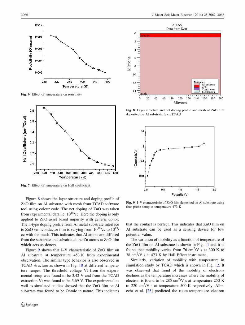
Figure 8 shows the layer structure and doping profile of
ZnO film on Al substrate with mesh from TCAD software
tool using colour code. The net doping of ZnO was taken
from experimental data i.e. 1018/cc. Here the doping is only
applied to ZnO asset based impurity with generic donor.
The n-type doping profile from Al metal substrate interface
to ZnO semiconductor film is varying from 1018/cc to 1013/
cc with the mesh. This indicates that Al atoms are diffused
from the substrate and substituted the Zn atoms at ZnO film
which acts as donors.
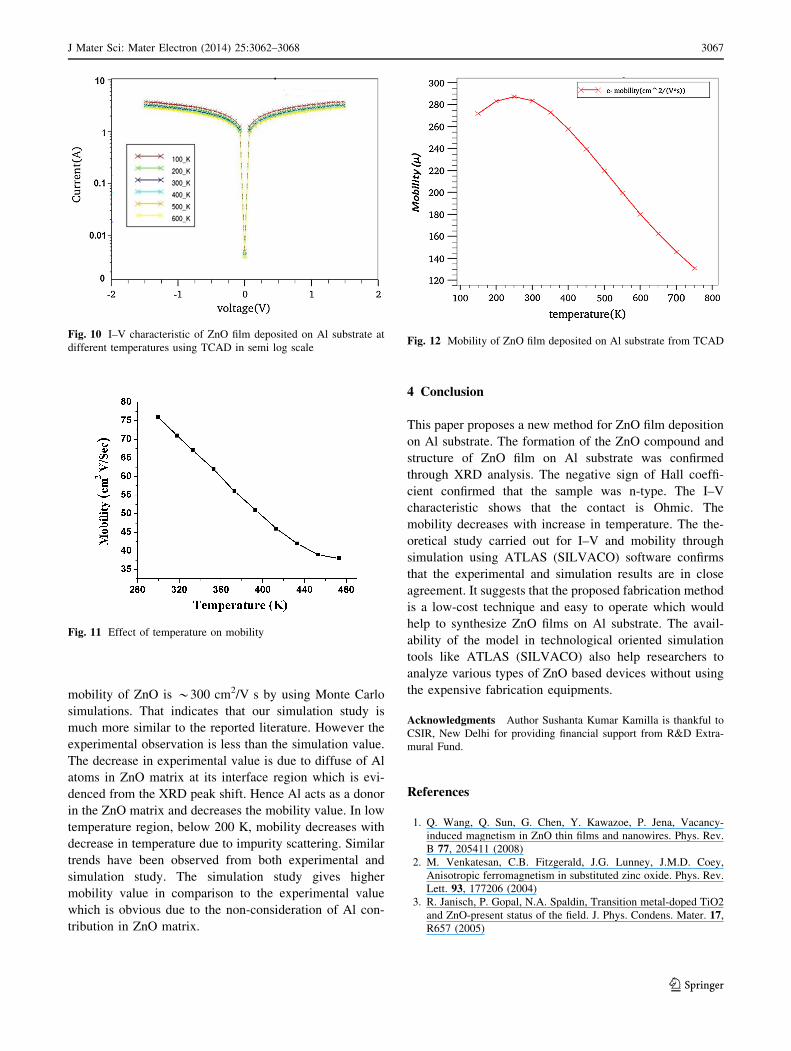
Figure 9 shows that I–V characteristic of ZnO film on
Al substrate at temperature 453 K from experimental
observation. The similar type behavior is also observed in
TCAD structure as shown in Fig. 10 at different tempera-
ture ranges. The threshold voltage Vt from the experi-
mental setup was found to be 3.42 V and from the TCAD
extraction Vt was found to be 3.69 V. The experimental as
well as simulated studies showed that the ZnO film on Al
substrate was found to be Ohmic in nature. This indicates
that the contact is perfect. This indicates that ZnO film on
Al substrate can be used as a sensing device for low
potential value.
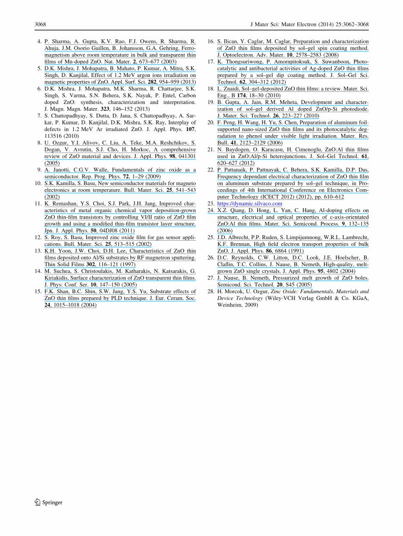
The variation of mobility as a function of temperature of
the ZnO film on Al substrate is shown in Fig. 11 and it is
found that mobility varies from 76 cm2/V s at 300 K to
38 cm2/V s at 473 K by Hall Effect instrument.
Similarly, variation of mobility with temperature in
simulation study by TCAD which is shown in Fig. 12. It
was observed that trend of the mobility of electrons
declines as the temperature increases where the mobility of
electron is found to be 285 cm2/V s at temperature 250 K
to 220 cm2/V s at temperature 500 K respectively. Albr-
echt et al. [25] predicted the room-temperature electron
Fig. 6 Effect of temperature on resistivity
Fig. 7 Effect of temperature on Hall coefficient
Fig. 8 Layer structure and net doping profile and mesh of ZnO film
deposited on Al substrate from TCAD
Fig. 9 I–V characteristic of ZnO film deposited on Al substrate using
four probe setup at temperature 473 K
3066 J Mater Sci: Mater Electron (2014) 25:3062–3068
123
mobility of ZnO is *300 cm2/V s by using Monte Carlo
simulations. That indicates that our simulation study is
much more similar to the reported literature. However the
experimental observation is less than the simulation value.
The decrease in experimental value is due to diffuse of Al
atoms in ZnO matrix at its interface region which is evi-
denced from the XRD peak shift. Hence Al acts as a donor
in the ZnO matrix and decreases the mobility value. In low
temperature region, below 200 K, mobility decreases with
decrease in temperature due to impurity scattering. Similar
trends have been observed from both experimental and
simulation study. The simulation study gives higher
mobility value in comparison to the experimental value
which is obvious due to the non-consideration of Al con-
tribution in ZnO matrix.
4 Conclusion
This paper proposes a new method for ZnO film deposition
on Al substrate. The formation of the ZnO compound and
structure of ZnO film on Al substrate was confirmed
through XRD analysis. The negative sign of Hall coeffi-
cient confirmed that the sample was n-type. The I–V
characteristic shows that the contact is Ohmic. The
mobility decreases with increase in temperature. The the-
oretical study carried out for I–V and mobility through
simulation using ATLAS (SILVACO) software confirms
that the experimental and simulation results are in close
agreement. It suggests that the proposed fabrication method
is a low-cost technique and easy to operate which would
help to synthesize ZnO films on Al substrate. The avail-
ability of the model in technological oriented simulation
tools like ATLAS (SILVACO) also help researchers to
analyze various types of ZnO based devices without using
the expensive fabrication equipments.
Acknowledgments Author Sushanta Kumar Kamilla is thankful to
CSIR, New Delhi for providing financial support from R&D Extra-
mural Fund.
References
1. Q. Wang, Q. Sun, G. Chen, Y. Kawazoe, P. Jena, Vacancy-
induced magnetism in ZnO thin films and nanowires. Phys. Rev.
B 77, 205411 (2008)
2. M. Venkatesan, C.B. Fitzgerald, J.G. Lunney, J.M.D. Coey,
Anisotropic ferromagnetism in substituted zinc oxide. Phys. Rev.
Lett. 93, 177206 (2004)
3. R. Janisch, P. Gopal, N.A. Spaldin, Transition metal-doped TiO2
and ZnO-present status of the field. J. Phys. Condens. Mater. 17,
R657 (2005)
Fig. 10 I–V characteristic of ZnO film deposited on Al substrate at
different temperatures using TCAD in semi log scale
Fig. 11 Effect of temperature on mobility
Fig. 12 Mobility of ZnO film deposited on Al substrate from TCAD
J Mater Sci: Mater Electron (2014) 25:3062–3068 3067
123
4. P. Sharma, A. Gupta, K.V. Rao, F.J. Owens, R. Sharma, R.
Ahuja, J.M. Osorio Guillen, B. Johansson, G.A. Gehring, Ferro-
magnetism above room temperature in bulk and transparent thin
films of Mn-doped ZnO. Nat. Mater. 2, 673–677 (2003)
5. D.K. Mishra, J. Mohapatra, B. Mahato, P. Kumar, A. Mitra, S.K.
Singh, D. Kanjilal, Effect of 1.2 MeV argon ions irradiation on
magnetic properties of ZnO. Appl. Surf. Sci. 282, 954–959 (2013)
6. D.K. Mishra, J. Mohapatra, M.K. Sharma, R. Chattarjee, S.K.
Singh, S. Varma, S.N. Behera, S.K. Nayak, P. Entel, Carbon
doped ZnO: synthesis, characterization and interpretation.
J. Magn. Magn. Mater. 323, 146–152 (2013)
7. S. Chattopadhyay, S. Dutta, D. Jana, S. Chattopadhyay, A. Sar-
kar, P. Kumar, D. Kanjilal, D.K. Mishra, S.K. Ray, Interplay of
defects in 1.2 MeV Ar irradiated ZnO. J. Appl. Phys. 107,
113516 (2010)
8. U. Ozgur, Y.I. Alivov, C. Liu, A. Teke, M.A. Reshchikov, S.
Dogan, V. Avrutin, S.J. Cho, H. Morkoc, A comprehensive
review of ZnO material and devices. J. Appl. Phys. 98, 041301
(2005)
9. A. Janotti, C.G.V. Walle, Fundamentals of zinc oxide as a
semiconductor. Rep. Prog. Phys. 72, 1–29 (2009)
10. S.K. Kamilla, S. Basu, New semiconductor materials for magneto
electronics at room temperature. Bull. Mater. Sci. 25, 541–543
(2002)
11. K. Remashan, Y.S. Choi, S.J. Park, J.H. Jang, Improved char-
acteristics of metal organic chemical vapor deposition-grown
ZnO thin-film transistors by controlling VI/II ratio of ZnO film
growth and using a modified thin-film transistor layer structure.
Jpn. J. Appl. Phys. 50, 04DJ08 (2011)
12. S. Roy, S. Basu, Improved zinc oxide film for gas sensor appli-
cations. Bull. Mater. Sci. 25, 513–515 (2002)
13. K.H. Yoon, J.W. Choi, D.H. Lee, Characteristics of ZnO thin
films deposited onto Al/Si substrates by RF magnetron sputtering.
Thin Solid Films 302, 116–121 (1997)
14. M. Suchea, S. Christoulakis, M. Katharakis, N. Katsarakis, G.
Kiriakidis, Surface characterization of ZnO transparent thin films.
J. Phys: Conf. Ser. 10, 147–150 (2005)
15. F.K. Shan, B.C. Shin, S.W. Jang, Y.S. Yu, Substrate effects of
ZnO thin films prepared by PLD technique. J. Eur. Ceram. Soc.
24, 1015–1018 (2004)
16. S. Ilican, Y. Caglar, M. Caglar, Preparation and characterization
of ZnO thin films deposited by sol–gel spin coating method.
J. Optoelectron. Adv. Mater. 10, 2578–2583 (2008)
17. K. Thongsuriwong, P. Amornpitoksuk, S. Suwanboon, Photo-
catalytic and antibacterial activities of Ag-doped ZnO thin films
prepared by a sol–gel dip coating method. J. Sol–Gel Sci.
Technol. 62, 304–312 (2012)
18. L. Znaidi, Sol–gel-deposited ZnO thin films: a review. Mater. Sci.
Eng., B 174, 18–30 (2010)
19. B. Gupta, A. Jain, R.M. Meheta, Development and character-
ization of sol–gel derived Al doped ZnO/p-Si photodiode.
J. Mater. Sci. Technol. 26, 223–227 (2010)
20. F. Peng, H. Wang, H. Yu, S. Chen, Preparation of aluminum foil-
supported nano-sized ZnO thin films and its photocatalytic deg-
radation to phenol under visible light irradiation. Mater. Res.
Bull. 41, 2123–2129 (2006)
21. N. Baydogen, O. Karacasu, H. Cimenoglu, ZnO:Al thin films
used in ZnO:Al/p-Si heterojunctions. J. Sol–Gel Technol. 61,
620–627 (2012)
22. P. Pattanaik, P. Pattnayak, C. Behera, S.K. Kamilla, D.P. Das,
Frequency dependant electrical characterization of ZnO thin film
on aluminum substrate prepared by sol–gel technique, in Pro-
ceedings of 4th International Conference on Electronics Com-
puter Technology (ICECT 2012) (2012), pp. 610–612
23. https://dynamic.silvaco.com
24. X.Z. Qiang, D. Hong, L. Yan, C. Hang, Al-doping effects on
structure, electrical and optical properties of c-axis-orientated
ZnO:Al thin films. Mater. Sci. Semicond. Process. 9, 132–135
(2006)
25. J.D. Albrecht, P.P. Ruden, S. Limpijumnong, W.R.L. Lambrecht,
K.F. Brennan, High field electron transport properties of bulk
ZnO. J. Appl. Phys. 86, 6864 (1991)
26. D.C. Reynolds, C.W. Litton, D.C. Look, J.E. Hoelscher, B.
Claflin, T.C. Collins, J. Nause, B. Nemeth, High-quality, melt-
grown ZnO single crystals. J. Appl. Phys. 95, 4802 (2004)
27. J. Nause, B. Nemeth, Pressurized melt growth of ZnO boles.
Semicond. Sci. Technol. 20, S45 (2005)
28. H. Morcok, U. Ozgur, Zinc Oxide: Fundamentals, Materials and
Device Technology (Wiley-VCH Verlag GmbH & Co. KGaA,
Weinheim, 2009)
3068 J Mater Sci: Mater Electron (2014) 25:3062–3068
123
Related Documents