Experiment # 8 EE 312 & 352 Introductory Electronics Laboratory November 1, 1999 Input Filter Regulation Load

Welcome message from author
This document is posted to help you gain knowledge. Please leave a comment to let me know what you think about it! Share it to your friends and learn new things together.
Transcript
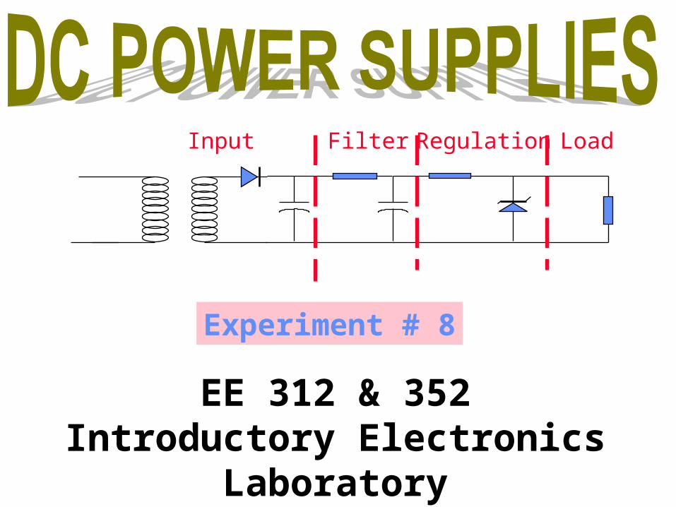
Experiment # 8
EE 312 & 352Introductory Electronics Laboratory
November 1, 1999
Input Filter Regulation Load
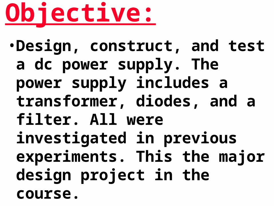
Objective:• Design, construct, and test a dc
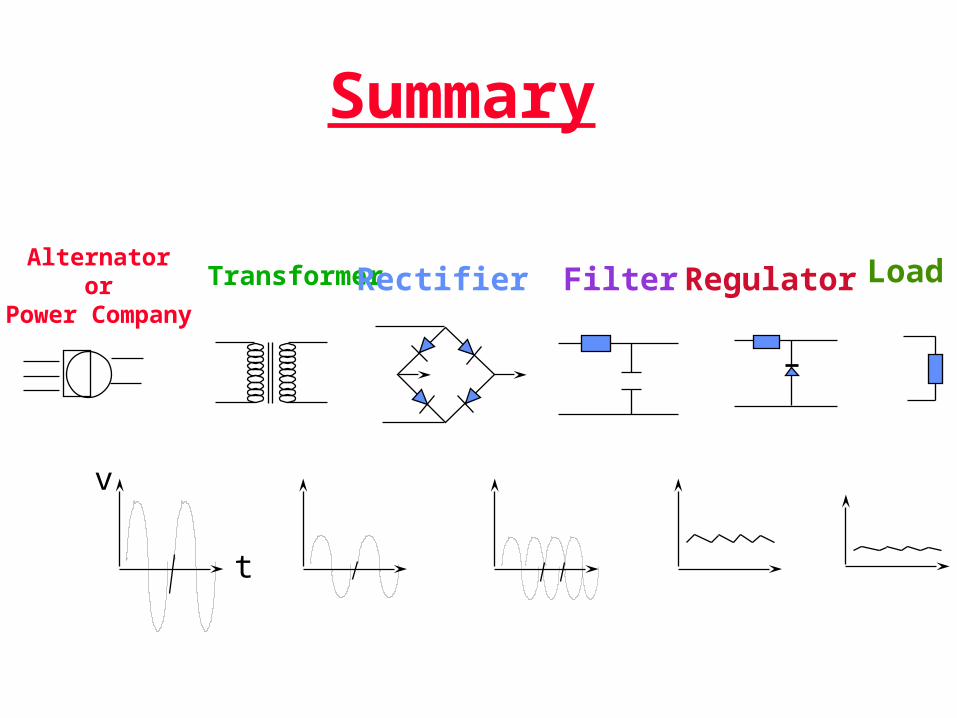
power supply. The power supply includes a transformer, diodes, and a filter. All were investigated in previous experiments. This the major design project in the course.

Transformer Filter RegulatorAlternator
orPower Company
Rectifier Load
t
v
Input: 120 VAC RMS, 60 Hz
Steps the input voltage up and down as needed
Convert the ac to a pulsing dc
Low-pass type for removing voltage variation
Keeps voltage constant regardless of load change
DC-VOLTAGE POWER SUPPLY OPERATION
Transformer Filter RegulatorRectifier LoadPower Company
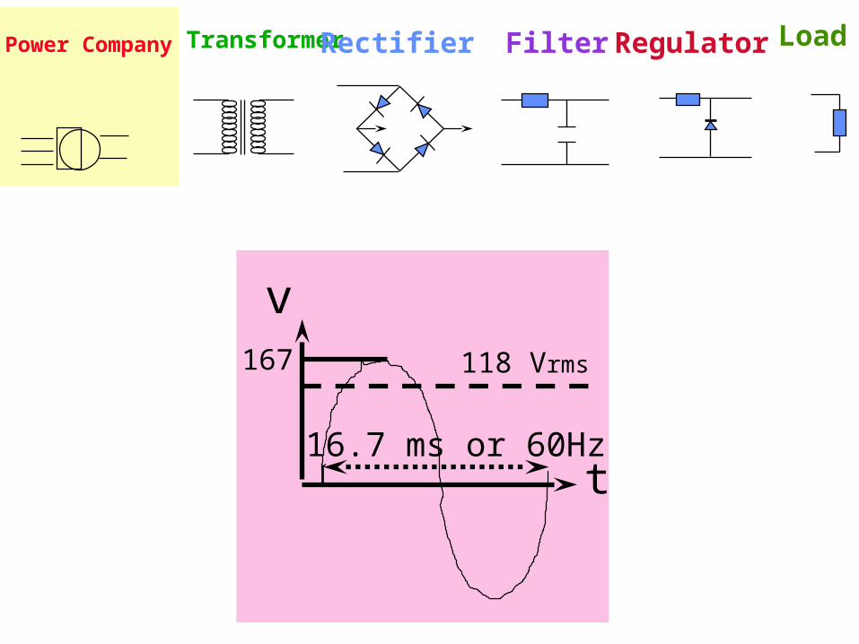
t
v167 118 Vrms
16.7 ms or 60Hz

Transformer Filter RegulatorRectifier LoadAlternatoror
Power Company
t
v167 118 Vrms
16.7 ms or 60Hz
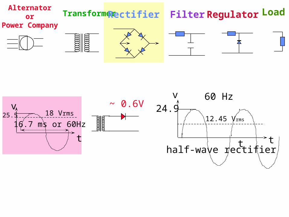
t
v25.5 18 Vrms
16.7 ms or 60Hz
Transformer Filter RegulatorRectifier LoadAlternatoror
Power Company
t
v
RLoad
RLoad
RLoad
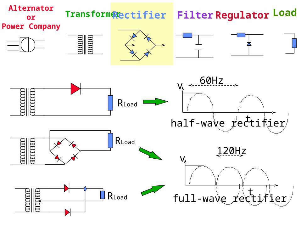
t
v
half-wave rectifier
full-wave rectifier
60Hz
120Hz
Transformer Filter RegulatorRectifier LoadAlternatoror
Power Company
t
v25.5 18 Vrms
16.7 ms or 60Hz
~ 0.6V
t
v
half-wave rectifier
24.960 Hz
12.45 Vrms
t
Transformer Filter RegulatorRectifier LoadAlternatoror
Power Company
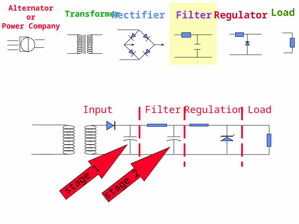
Input Filter Regulation Load
stage 1
stage 2

t
v
tt
v
t
et
RC
Vmaxripple
Input Filter Regulation Load
stage 1
without C with C
C
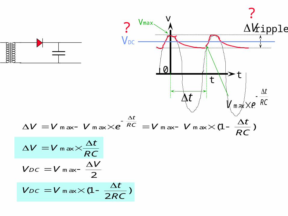
t
vVmaxripple
t
VDC
0
tV e
t
RCmax
V V V e V Vt
RC
V Vt
RC
V VV
V Vt
RC
t
RC
DC
DC
max max max max
max
max
max
( )
( )
1
2
12
V??

stage 2
V across R < 25% of Vinput
1 1
3CR
One or more filter sections are usually used to reduce the amplitude of the ripple. The filter used in this experiment is a single-section low-pass RC filter.
Input Filter Regulation Load
C
R
Vinput
usually tolerable
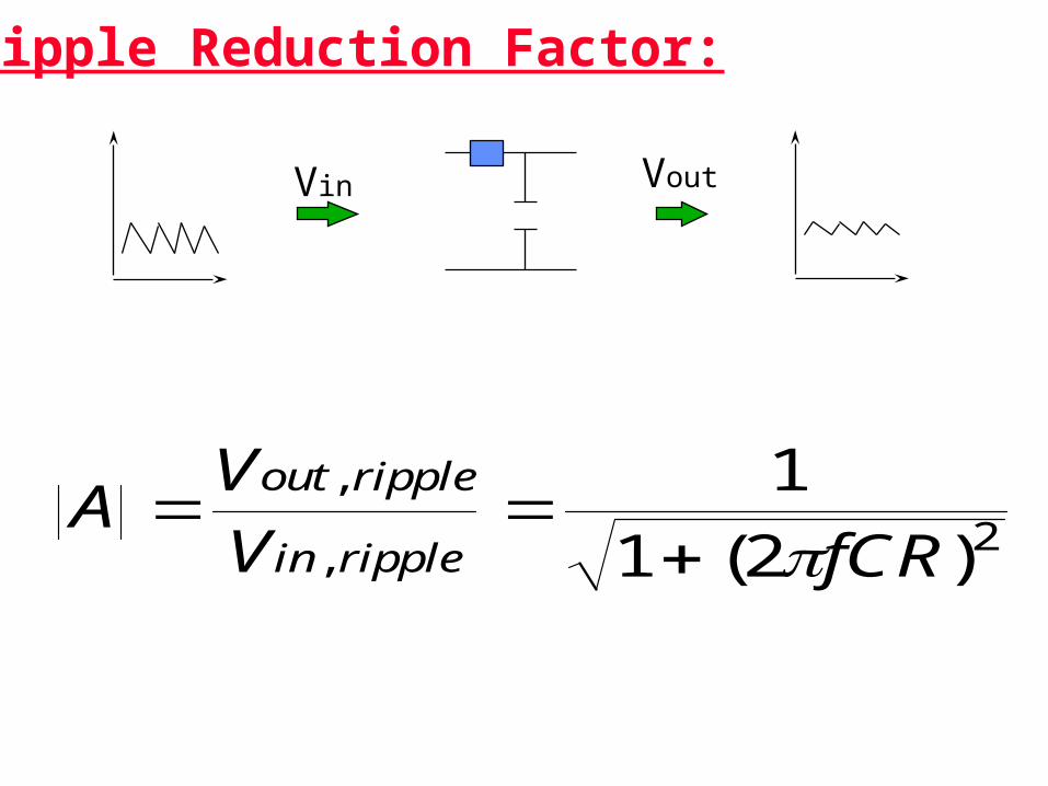
Ripple Reduction Factor:
AV
V fCR
out ripple
in ripple
,
, ( )
1
1 2 2
Vin Vout
Transformer Filter RegulatorRectifier LoadAlternatoror
Power Company
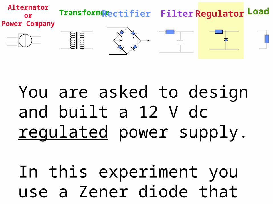
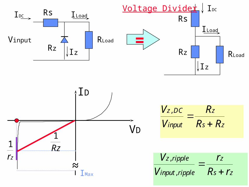
You are asked to design and built a 12 V dc regulated power supply.
In this experiment you use a Zener diode that breaks down at 12 V.
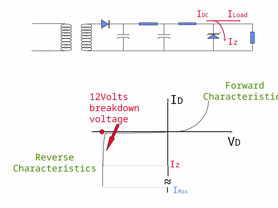
ID
VD
ForwardCharacteristics
ReverseCharacteristics
12Voltsbreakdownvoltage
~~ IMax
Iz
ILoadIDC
Iz
ID
VD
~~ IMax
RLoad
Rs
Rz
IDC
ILoad
Iz
RLoad
Rs
Rz
IDC ILoad
Iz
Voltage Divider
=
V
V
R
R R
z DC
input
z
s z
,
Vinput
V
V
r
R r
z ripple
input ripple
z
s z
,
,
1
Rz1
rz
Transformer Filter RegulatorAlternator
orPower Company
Rectifier Load
t
v
Summary
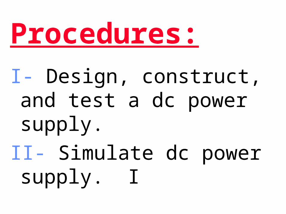
Procedures:
I- Design, construct, and test a dc power supply.
II- Simulate dc power supply. I
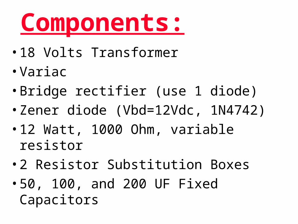
Components:• 18 Volts Transformer
• Variac
• Bridge rectifier (use 1 diode)
• Zener diode (Vbd=12Vdc, 1N4742)
• 12 Watt, 1000 Ohm, variable resistor
• 2 Resistor Substitution Boxes
• 50, 100, and 200 UF Fixed Capacitors

1- Design, construct, test a dc power supply
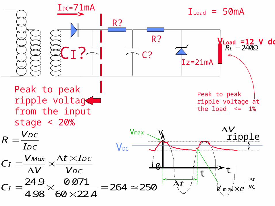
Suggestion: Zener diode current = 21 mA (At this current, the Zener resistance is 9 ohms)
VLoad =12 V dc
ILoad = 50mA
Peak to peak ripple voltage from the input stage < 20%
Peak to peak ripple voltage at the load <= 1%
R? R?
C? R?C?

VLoad =12 V dc
ILoad = 50mA
Peak to peak ripple voltage from the input stage < 20%
Peak to peak ripple voltage at the load <= 1%
R? R?
C? RLoad?C?
RV
I
V
mALoad
Load
Load
12
50240

VLoad =12 V dc
ILoad = 50mA
Peak to peak ripple voltage from the input stage < 20%
Peak to peak ripple voltage at the load <= 1%
R?
R?
C?C?RL 240
IDC
IDC
Iz=21mA
I I I mA mA mADC Load z 50 21 71
VLoad =12 V dc
ILoad = 50mA
Peak to peak ripple voltage from the input stage < 20%
Peak to peak ripple voltage at the load <= 1%
R?
R?
C?CI? RL 240
IDC=71mA
Iz=21mA
t
vVmaxripple
t
VDC
0
tV e
t
RCmax
VR
V
I
CV
V
t I
V
C
DC
DC
IMax DC
DC
I
24 9
4 98
0 071
60 22264 250
.
.
.
.4
t
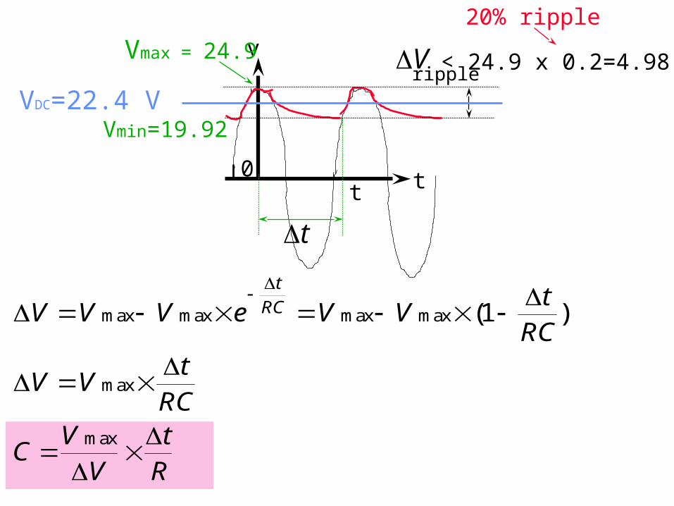
vVmax = 24.9ripple
t
VDC=22.4 V
0
t
V < 24.9 x 0.2=4.98 V
20% ripple
Vmin=19.92
V V V e V Vt
RC
V Vt
RC
CV
V
t
R
t
RC
max max max max
max
max
( )1
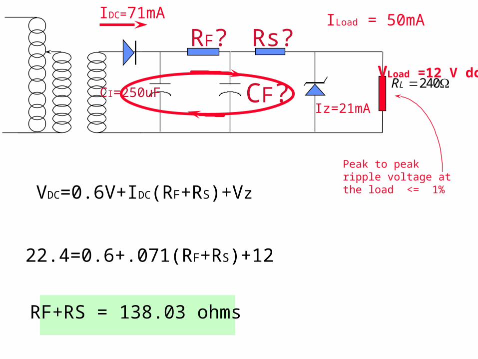
VLoad =12 V dc
ILoad = 50mA
Peak to peak ripple voltage at the load <= 1%
RF? Rs?
CF?CI=250uFRL 240
IDC=71mA
Iz=21mA
VDC=0.6V+IDC(RF+RS)+Vz
22.4=0.6+.071(RF+RS)+12
RF+RS = 138.03 ohms
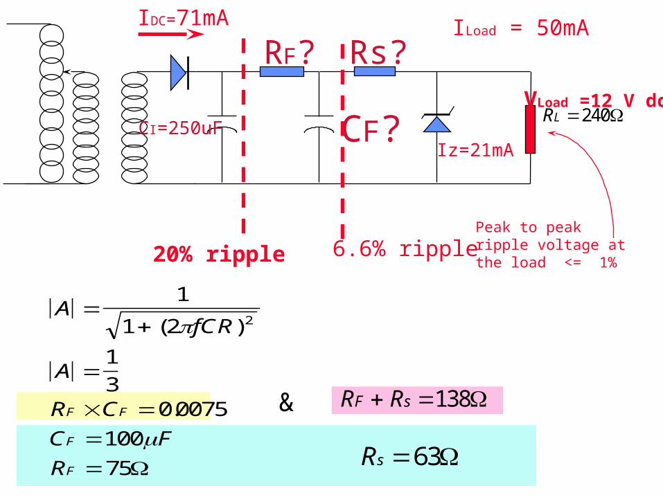
VLoad =12 V dc
ILoad = 50mA
Peak to peak ripple voltage at the load <= 1%
RF? Rs?
CF?CI=250uFRL 240
IDC=71mA
Iz=21mA
20% ripple 6.6% ripple
AfCR
A
R C
C F
R
F F
F
F
1
1 2
1
30 0075
100
75
2( )
.
R RF s 138&
Rs 63
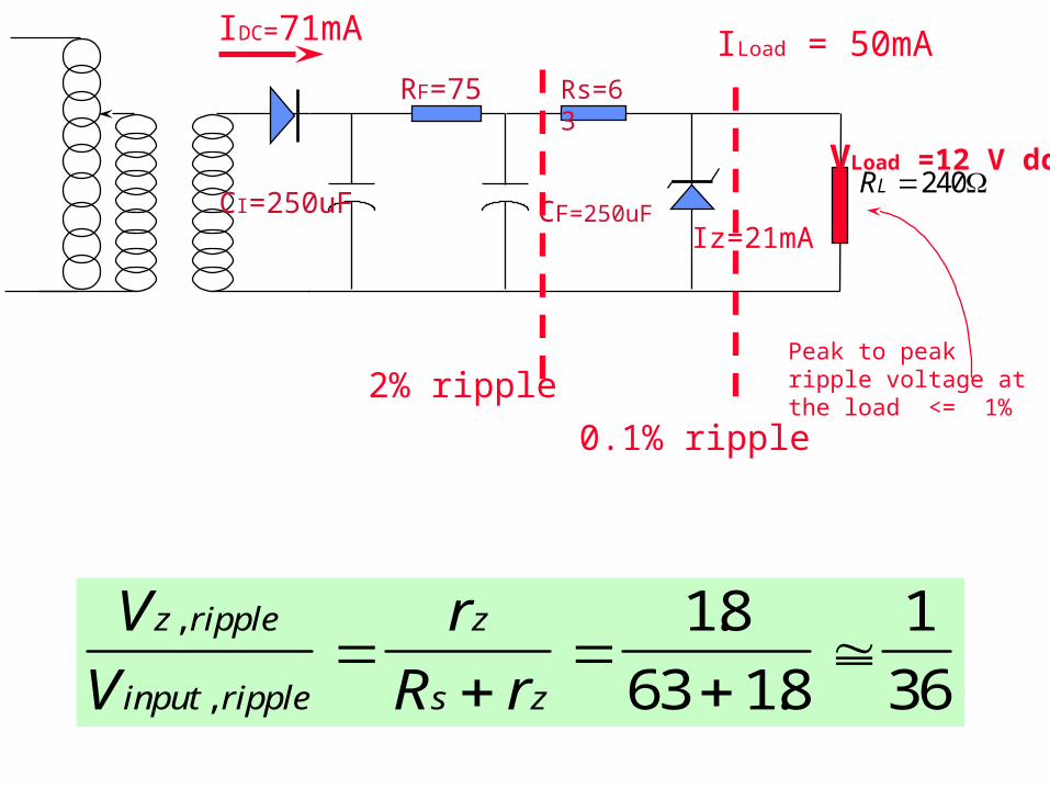
V
V
r
R r
z ripple
input ripple
z
s z
,
,
.
.
18
63 18
1
36
VLoad =12 V dc
ILoad = 50mA
Peak to peak ripple voltage at the load <= 1%
RF=75 Rs=63
CF=250uFCI=250uFRL 240
IDC=71mA
Iz=21mA
0.1% ripple
2% ripple
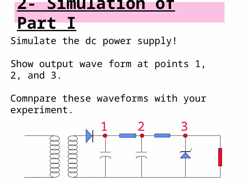
2- Simulation of Part I
Simulate the dc power supply!
Show output wave form at points 1, 2, and 3.
Comnpare these waveforms with your experiment.
1 2 3
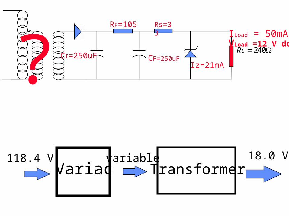
VLoad =12 V dcILoad = 50mA
RF=105 Rs=33
CF=250uFCI=250uFRL 240
Iz=21mA?Variac Transformer
18.0 V118.4 V variable
Report is requiredfor EE 312 & 352
Related Documents