Experiment #6a: Analog-to-Digital Convertor Part 1 (Part 2 is further down and has its own table of contents) Emma Gray, 36396166 Partner: Julia Rosenrauch Table of Contents Experiment #6a: Analog-to-Digital Convertor......................................................................................................... 1 Part 1 (Part 2 is further down and has its own table of contents).......................................................................... 1 Emma Gray, 36396166....................................................................................................................................... 1 Partner: Julia Rosenrauch...................................................................................................................................1 1. Objective............................................................................................................................................................. 1 2. Background......................................................................................................................................................... 1 3. Components........................................................................................................................................................ 2 3.1 Trigger Pulse Generator............................................................................................................................... 3 3.1.1 Square Wave Oscillator (3a)..................................................................................................................... 8 3.1.2 Short Pulse Rectifier (3b)........................................................................................................................ 10 3.1.3 Complete Setup: Trigger Pulse Generator.............................................................................................. 11 1. Objective The objective of this lab is to create an analog-to-digital converter, or ADC, that is capable of transforming an analog voltage input into a digital (binary) representation. This lab will involve components that we have already worked with in this class, such as NOT and NAND gates, counters, flip-flops and op- amps, as well as new components such as Schmitt-trigger inverters and a new type of transistor switch. 2. Background From sound to power to luminosity, analog signals can be found everywhere in the natural world. However, in order for these signals to be stored, loaded and analyzed by computers, we require a means to discretize them into binary values that represent their magnitudes. Our analog-to-digital converter uses an analog-to-time converter to do exactly this. From a technical standpoint, the process can be generalized as follows: a series of "gate pulses" are generated with a frequency that is proportional to the magnitude of the system input voltage, and the rising edge of one of these gate pulses triggers a constant-frequency clock pulse, hooked up to a counter, to quantify the number of clock pulses that fit under a gate pulse. This number can be converted to represent the magnitude of the input signal, and the result from that becomes the output of the system, updating with each new gate pulse. 1

Welcome message from author
This document is posted to help you gain knowledge. Please leave a comment to let me know what you think about it! Share it to your friends and learn new things together.
Transcript
Experiment #6a: Analog-to-Digital Convertor
Part 1 (Part 2 is further down and has its own table of contents)
Emma Gray, 36396166
Partner: Julia Rosenrauch
Table of Contents
Experiment #6a: Analog-to-Digital Convertor......................................................................................................... 1Part 1 (Part 2 is further down and has its own table of contents)..........................................................................1
Emma Gray, 36396166.......................................................................................................................................1Partner: Julia Rosenrauch...................................................................................................................................1
1. Objective............................................................................................................................................................. 12. Background......................................................................................................................................................... 13. Components........................................................................................................................................................ 2
3.1 Trigger Pulse Generator............................................................................................................................... 33.1.1 Square Wave Oscillator (3a)..................................................................................................................... 83.1.2 Short Pulse Rectifier (3b)........................................................................................................................ 103.1.3 Complete Setup: Trigger Pulse Generator.............................................................................................. 11
1. Objective
The objective of this lab is to create an analog-to-digital converter, or ADC, that is capable oftransforming an analog voltage input into a digital (binary) representation. This lab will involve componentsthat we have already worked with in this class, such as NOT and NAND gates, counters, flip-flops and op-amps, as well as new components such as Schmitt-trigger inverters and a new type of transistor switch.
2. Background
From sound to power to luminosity, analog signals can be found everywhere in the natural world.However, in order for these signals to be stored, loaded and analyzed by computers, we require a means todiscretize them into binary values that represent their magnitudes.
Our analog-to-digital converter uses an analog-to-time converter to do exactly this. From a technicalstandpoint, the process can be generalized as follows: a series of "gate pulses" are generated with afrequency that is proportional to the magnitude of the system input voltage, and the rising edge of one ofthese gate pulses triggers a constant-frequency clock pulse, hooked up to a counter, to quantify the numberof clock pulses that fit under a gate pulse. This number can be converted to represent the magnitude of theinput signal, and the result from that becomes the output of the system, updating with each new gate pulse.
1
Emma Gray
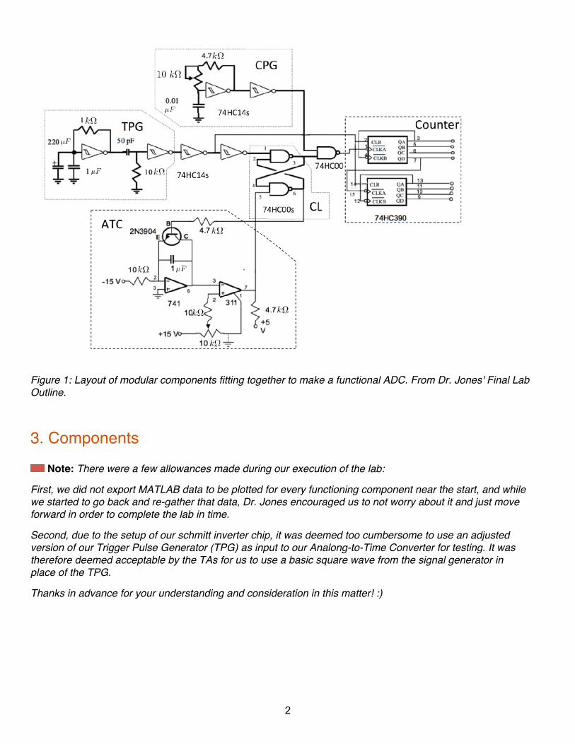
Figure 1: Layout of modular components fitting together to make a functional ADC. From Dr. Jones' Final LabOutline.
3. Components
Note: There were a few allowances made during our execution of the lab:
First, we did not export MATLAB data to be plotted for every functioning component near the start, and whilewe started to go back and re-gather that data, Dr. Jones encouraged us to not worry about it and just moveforward in order to complete the lab in time.
Second, due to the setup of our schmitt inverter chip, it was deemed too cumbersome to use an adjustedversion of our Trigger Pulse Generator (TPG) as input to our Analong-to-Time Converter for testing. It wastherefore deemed acceptable by the TAs for us to use a basic square wave from the signal generator inplace of the TPG.
Thanks in advance for your understanding and consideration in this matter! :)
2
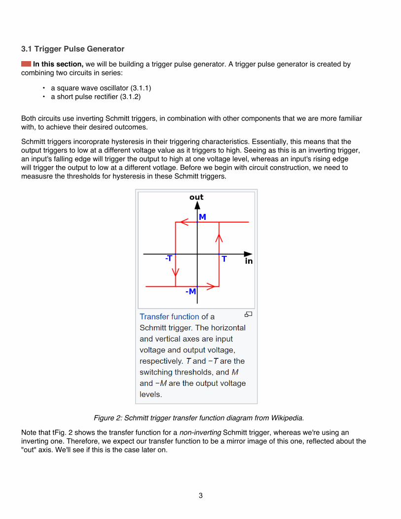
3.1 Trigger Pulse Generator
In this section, we will be building a trigger pulse generator. A trigger pulse generator is created bycombining two circuits in series:
• a square wave oscillator (3.1.1) • a short pulse rectifier (3.1.2)
Both circuits use inverting Schmitt triggers, in combination with other components that we are more familiarwith, to achieve their desired outcomes.
Schmitt triggers incoroprate hysteresis in their triggering characteristics. Essentially, this means that theoutput triggers to low at a different voltage value as it triggers to high. Seeing as this is an inverting trigger,an input's falling edge will trigger the output to high at one voltage level, whereas an input's rising edgewill trigger the output to low at a different votlage. Before we begin with circuit construction, we need tomeasusre the thresholds for hysteresis in these Schmitt triggers.
Figure 2: Schmitt trigger transfer function diagram from Wikipedia.
Note that tFig. 2 shows the transfer function for a non-inverting Schmitt trigger, whereas we're using aninverting one. Therefore, we expect our transfer function to be a mirror image of this one, reflected about the"out" axis. We'll see if this is the case later on.
3
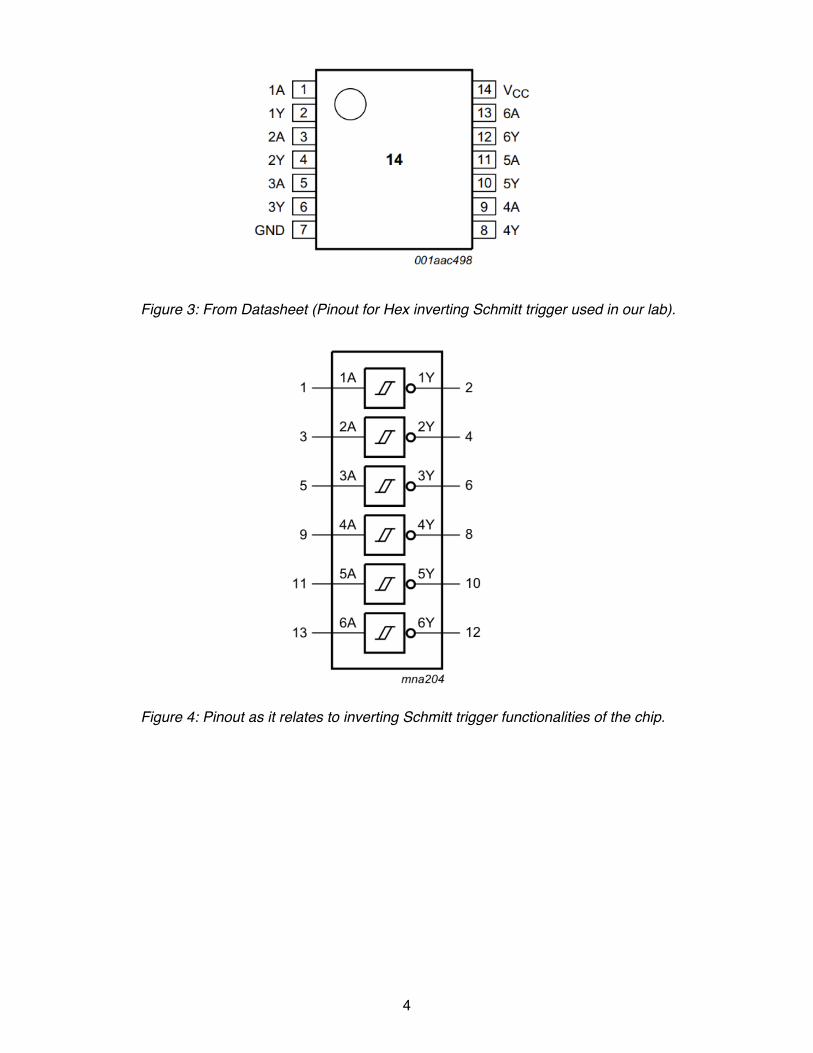
Figure 3: From Datasheet (Pinout for Hex inverting Schmitt trigger used in our lab).
Figure 4: Pinout as it relates to inverting Schmitt trigger functionalities of the chip.
4
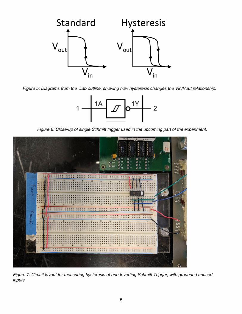
Figure 5: Diagrams from the Lab outline, showing how hysteresis changes the Vin/Vout relationship.
Figure 6: Close-up of single Schmitt trigger used in the upcoming part of the experiment.
Figure 7: Circuit layout for measuring hysteresis of one Inverting Schmitt Trigger, with grounded unusedinputs.
5
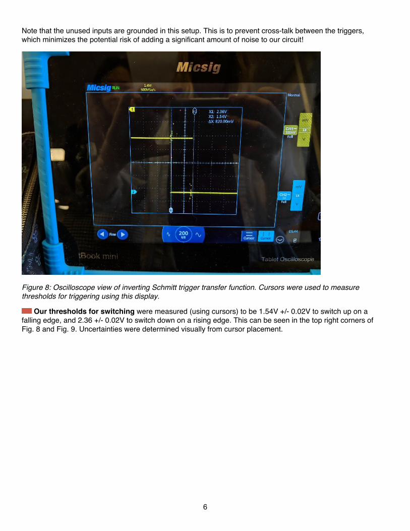
Note that the unused inputs are grounded in this setup. This is to prevent cross-talk between the triggers,which minimizes the potential risk of adding a significant amount of noise to our circuit!
Figure 8: Oscilloscope view of inverting Schmitt trigger transfer function. Cursors were used to measurethresholds for triggering using this display.
Our thresholds for switching were measured (using cursors) to be 1.54V +/- 0.02V to switch up on afalling edge, and 2.36 +/- 0.02V to switch down on a rising edge. This can be seen in the top right corners ofFig. 8 and Fig. 9. Uncertainties were determined visually from cursor placement.
6
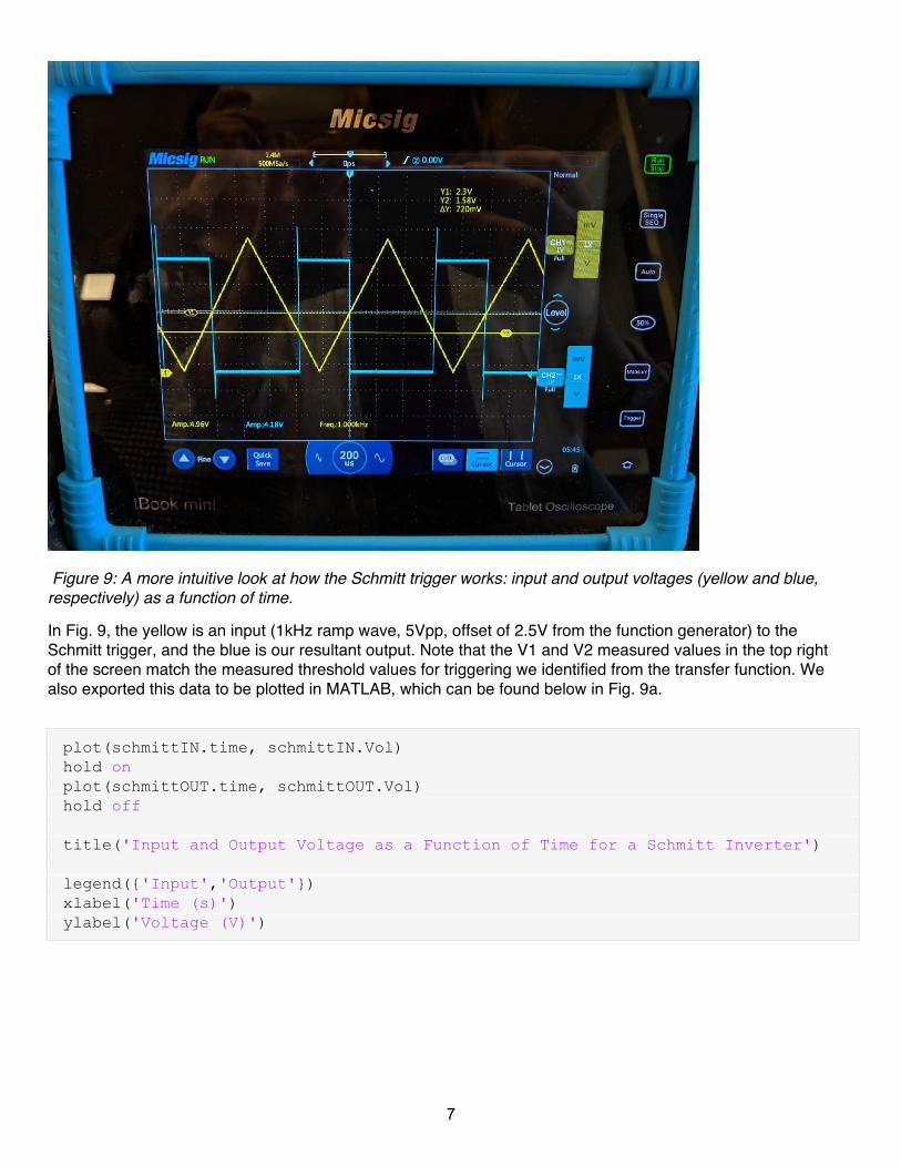
Figure 9: A more intuitive look at how the Schmitt trigger works: input and output voltages (yellow and blue,respectively) as a function of time.
In Fig. 9, the yellow is an input (1kHz ramp wave, 5Vpp, offset of 2.5V from the function generator) to theSchmitt trigger, and the blue is our resultant output. Note that the V1 and V2 measured values in the top rightof the screen match the measured threshold values for triggering we identified from the transfer function. Wealso exported this data to be plotted in MATLAB, which can be found below in Fig. 9a.
plot(schmittIN.time, schmittIN.Vol)hold onplot(schmittOUT.time, schmittOUT.Vol)hold off title('Input and Output Voltage as a Function of Time for a Schmitt Inverter') legend({'Input','Output'})xlabel('Time (s)')ylabel('Voltage (V)')
7
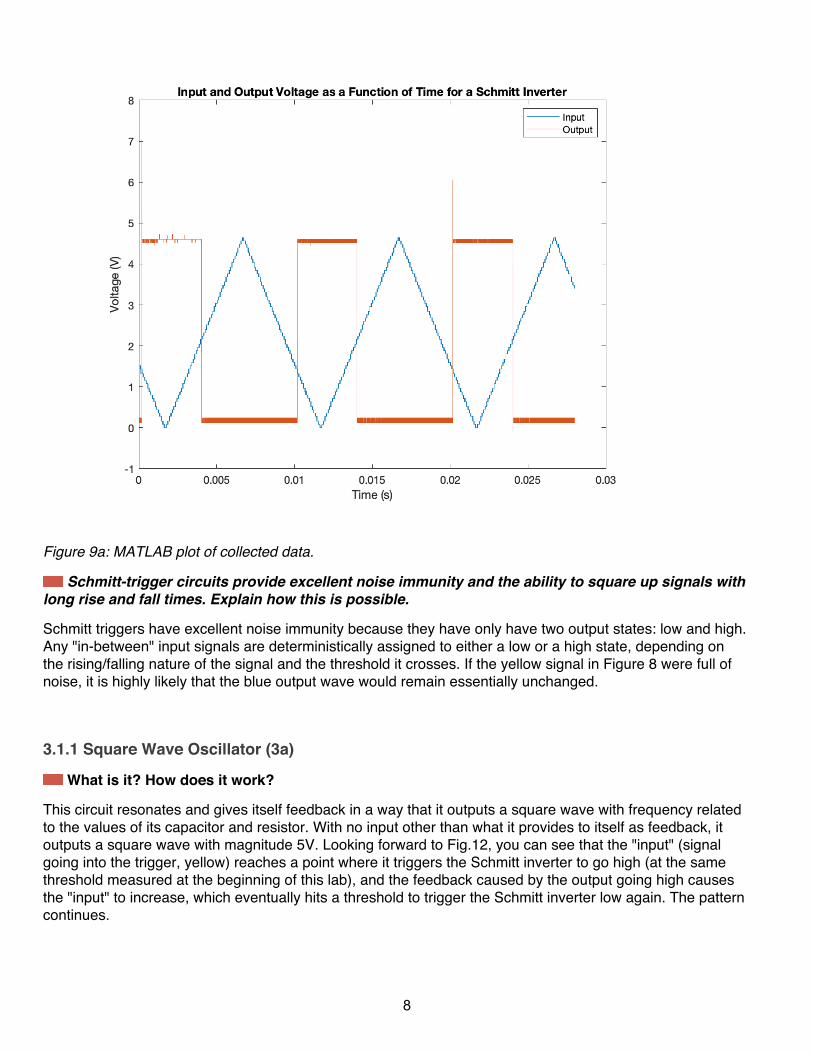
Figure 9a: MATLAB plot of collected data.
Schmitt-trigger circuits provide excellent noise immunity and the ability to square up signals withlong rise and fall times. Explain how this is possible.
Schmitt triggers have excellent noise immunity because they have only have two output states: low and high.Any "in-between" input signals are deterministically assigned to either a low or a high state, depending onthe rising/falling nature of the signal and the threshold it crosses. If the yellow signal in Figure 8 were full ofnoise, it is highly likely that the blue output wave would remain essentially unchanged.
3.1.1 Square Wave Oscillator (3a)
What is it? How does it work?
This circuit resonates and gives itself feedback in a way that it outputs a square wave with frequency relatedto the values of its capacitor and resistor. With no input other than what it provides to itself as feedback, itoutputs a square wave with magnitude 5V. Looking forward to Fig.12, you can see that the "input" (signalgoing into the trigger, yellow) reaches a point where it triggers the Schmitt inverter to go high (at the samethreshold measured at the beginning of this lab), and the feedback caused by the output going high causesthe "input" to increase, which eventually hits a threshold to trigger the Schmitt inverter low again. The patterncontinues.
8
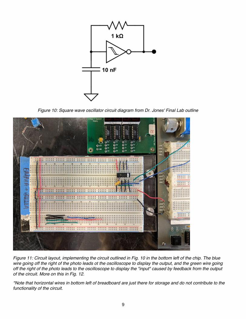
Figure 10: Square wave oscillator circuit diagram from Dr. Jones' Final Lab outline
Figure 11: Circuit layout, implementing the circuit outlined in Fig. 10 in the bottom left of the chip. The bluewire going off the right of the photo leads ot the oscilloscope to display the output, and the green wire goingoff the right of the photo leads to the oscilloscope to display the "input" caused by feedback from the outputof the circuit. More on this in Fig. 12.
*Note that horizontal wires in bottom left of breadboard are just there for storage and do not contribute to thefunctionality of the circuit.
9
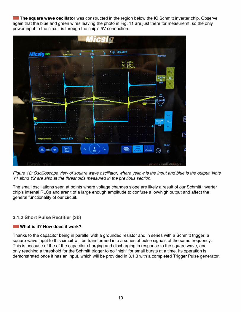
The square wave oscillator was constructed in the region below the IC Schmitt inverter chip. Observeagain that the blue and green wires leaving the photo in Fig. 11 are just there for measuremt, so the onlypower input to the circuit is through the chip's 5V connection.
Figure 12: Oscilloscope view of square wave oscillator, where yellow is the input and blue is the output. NoteY1 abnd Y2 are also at the thresholds measured in the previous section.
The small oscillations seen at points where voltage changes slope are likely a result of our Schmitt inverterchip's internal RLCs and aren't of a large enough amplitude to confuse a low/high output and affect thegeneral functionality of our circuit.
3.1.2 Short Pulse Rectifier (3b)
What is it? How does it work?
Thanks to the capacitor being in parallel with a grounded resistor and in series with a Schmitt trigger, asquare wave input to this circuit will be transformed into a series of pulse signals of the same frequency.This is because of the of the capacitor charging and discharging in response to the square wave, andonly reaching a threshold for the Schmitt trigger to go "high" for small bursts at a time. Its operation isdemonstrated once it has an input, which will be provided in 3.1.3 with a completed Trigger Pulse generator.
10
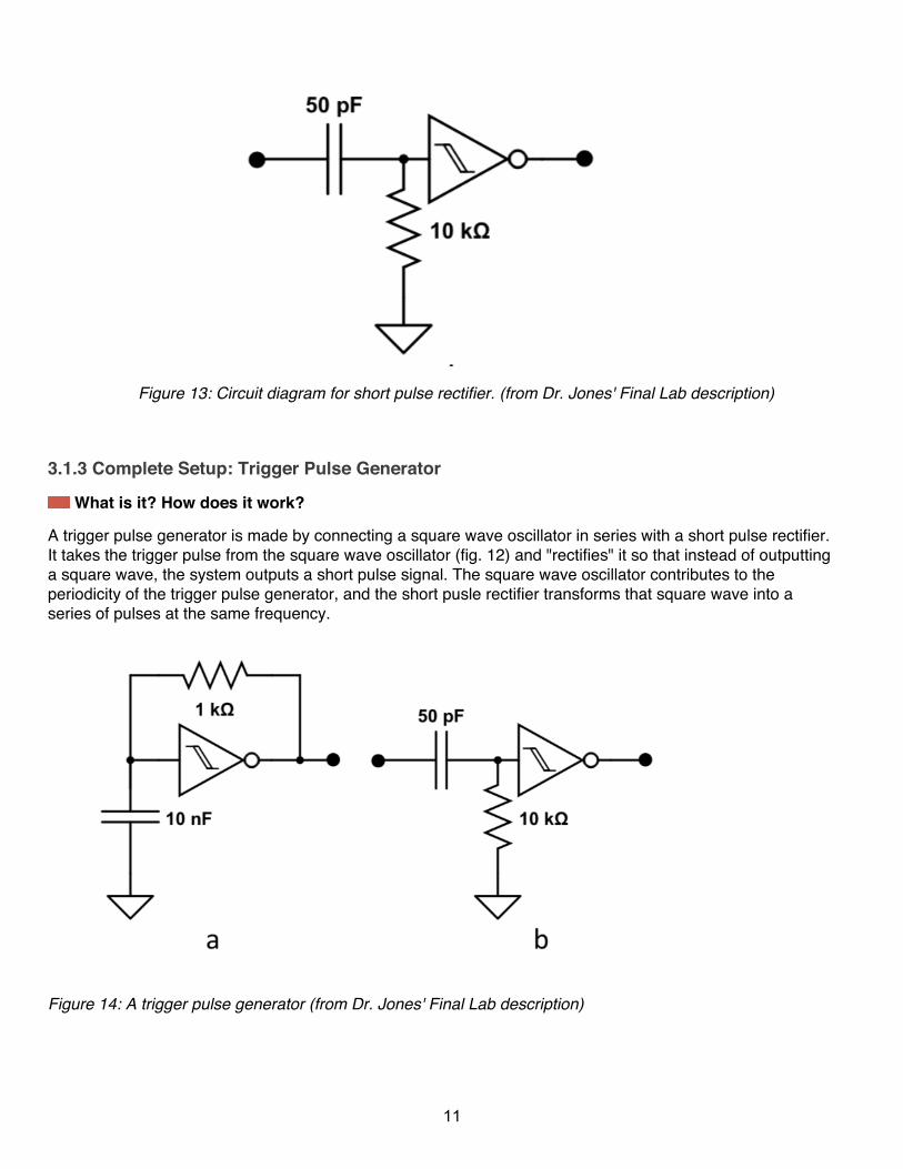
Figure 13: Circuit diagram for short pulse rectifier. (from Dr. Jones' Final Lab description)
3.1.3 Complete Setup: Trigger Pulse Generator
What is it? How does it work?
A trigger pulse generator is made by connecting a square wave oscillator in series with a short pulse rectifier.It takes the trigger pulse from the square wave oscillator (fig. 12) and "rectifies" it so that instead of outputtinga square wave, the system outputs a short pulse signal. The square wave oscillator contributes to theperiodicity of the trigger pulse generator, and the short pusle rectifier transforms that square wave into aseries of pulses at the same frequency.
Figure 14: A trigger pulse generator (from Dr. Jones' Final Lab description)
11
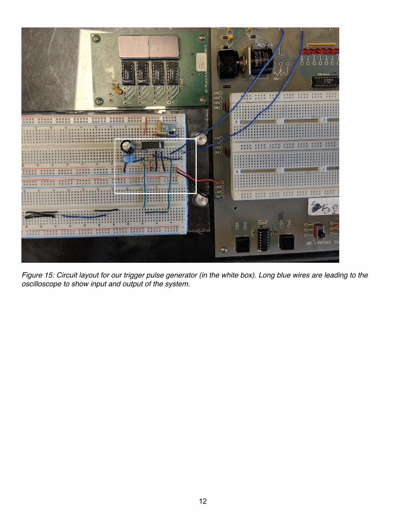
Figure 15: Circuit layout for our trigger pulse generator (in the white box). Long blue wires are leading to theoscilloscope to show input and output of the system.
12
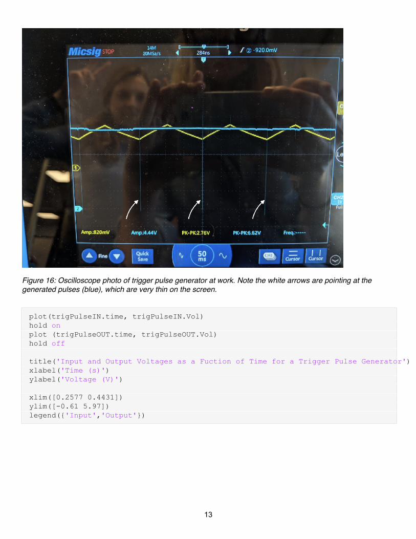
Figure 16: Oscilloscope photo of trigger pulse generator at work. Note the white arrows are pointing at thegenerated pulses (blue), which are very thin on the screen.
plot(trigPulseIN.time, trigPulseIN.Vol)hold onplot (trigPulseOUT.time, trigPulseOUT.Vol)hold off title('Input and Output Voltages as a Fuction of Time for a Trigger Pulse Generator')xlabel('Time (s)')ylabel('Voltage (V)') xlim([0.2577 0.4431])ylim([-0.61 5.97])legend({'Input','Output'})
13
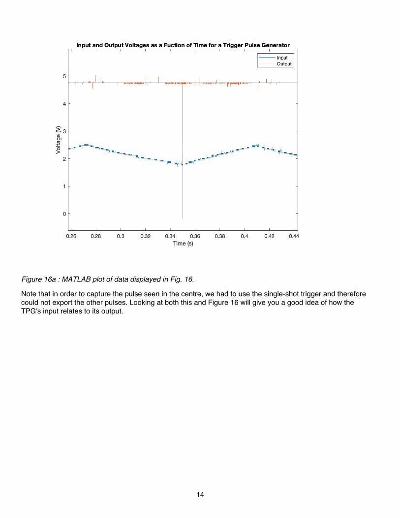
Figure 16a : MATLAB plot of data displayed in Fig. 16.
Note that in order to capture the pulse seen in the centre, we had to use the single-shot trigger and thereforecould not export the other pulses. Looking at both this and Figure 16 will give you a good idea of how theTPG's input relates to its output.
14
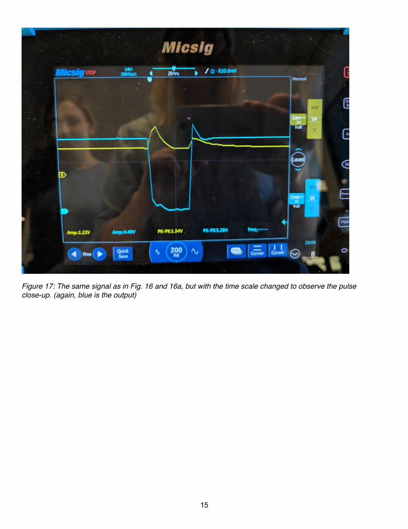
Figure 17: The same signal as in Fig. 16 and 16a, but with the time scale changed to observe the pulseclose-up. (again, blue is the output)
15
Experiment #6a: Analog-to-Digital Convertor
Part 2
Emma Gray, 36396166
Partner: Julia Rosenrauch
Table of Contents
Experiment #6a: Analog-to-Digital Convertor......................................................................................................... 1Part 2.......................................................................................................................................................................1
Emma Gray, 36396166.......................................................................................................................................1Partner: Julia Rosenrauch...................................................................................................................................1
3. Components (continued from Part 1)................................................................................................................. 13.2 Clock Pulse Generator..................................................................................................................................13.3 Counter..........................................................................................................................................................3
3. Components (continued from Part 1)
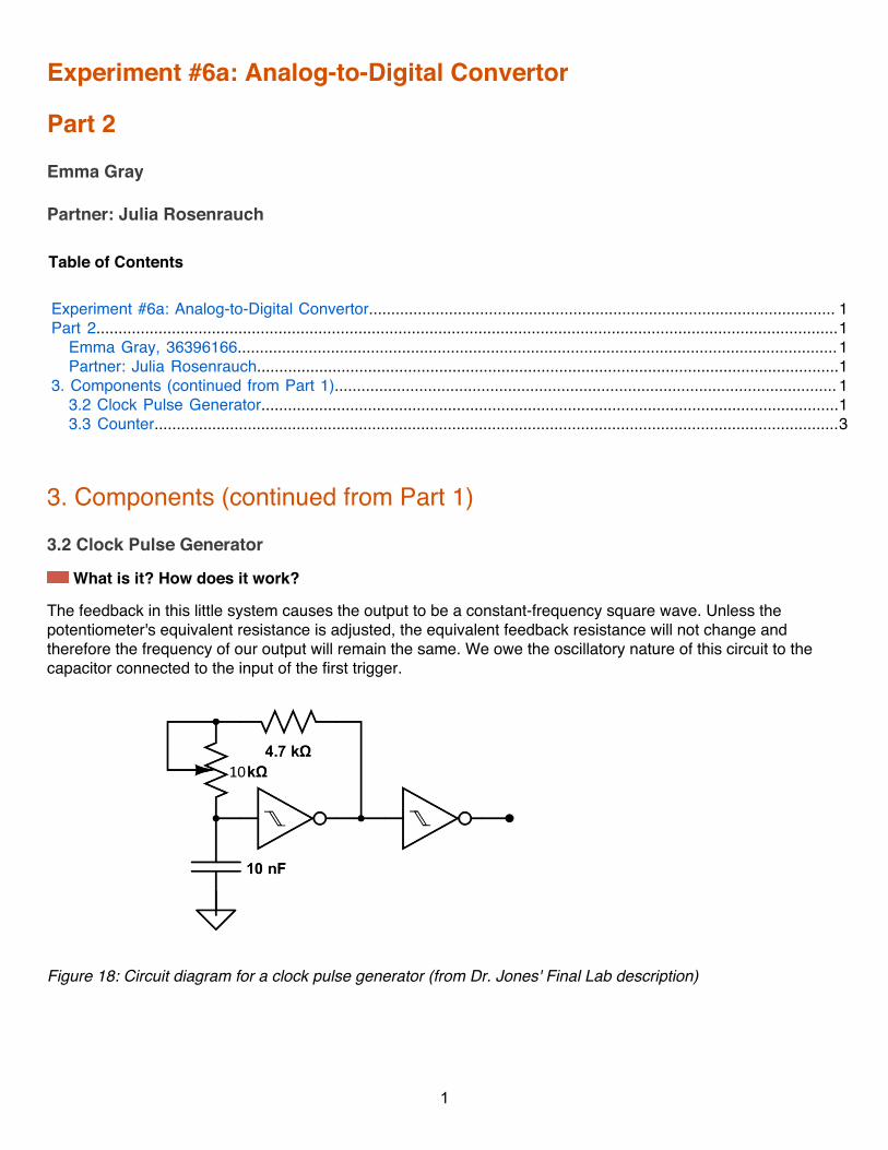
3.2 Clock Pulse Generator
What is it? How does it work?
The feedback in this little system causes the output to be a constant-frequency square wave. Unless thepotentiometer's equivalent resistance is adjusted, the equivalent feedback resistance will not change andtherefore the frequency of our output will remain the same. We owe the oscillatory nature of this circuit to thecapacitor connected to the input of the first trigger.
Figure 18: Circuit diagram for a clock pulse generator (from Dr. Jones' Final Lab description)
1
Emma Gray
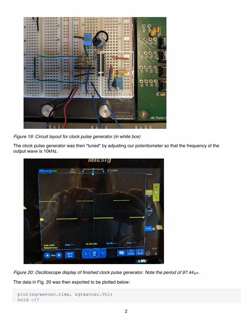
Figure 19: Circuit layout for clock pulse generator (in white box)
The clock pulse generator was then "tuned" by adjusting our potentiometer so that the frequency of theoutput wave is 10kHz.
Figure 20: Oscilloscope display of finished clock pulse generator. Note the period of 97.44 .
The data in Fig. 20 was then exported to be plotted below:
plot(sqrwavosc.time, sqrwavosc.Vol)hold off
2
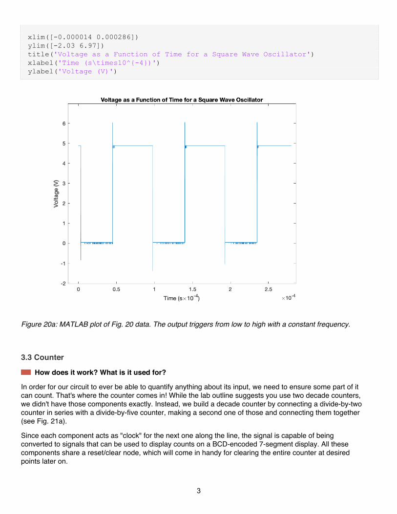
xlim([-0.000014 0.000286])ylim([-2.03 6.97])title('Voltage as a Function of Time for a Square Wave Oscillator')xlabel('Time (s\times10^{-4})')ylabel('Voltage (V)')
Figure 20a: MATLAB plot of Fig. 20 data. The output triggers from low to high with a constant frequency.
3.3 Counter
How does it work? What is it used for?
In order for our circuit to ever be able to quantify anything about its input, we need to ensure some part of itcan count. That's where the counter comes in! While the lab outline suggests you use two decade counters,we didn't have those components exactly. Instead, we build a decade counter by connecting a divide-by-twocounter in series with a divide-by-five counter, making a second one of those and connecting them together(see Fig. 21a).
Since each component acts as "clock" for the next one along the line, the signal is capable of beingconverted to signals that can be used to display counts on a BCD-encoded 7-segment display. All thesecomponents share a reset/clear node, which will come in handy for clearing the entire counter at desiredpoints later on.
3
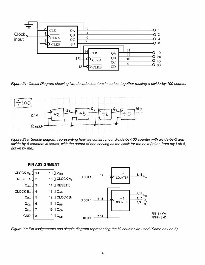
Figure 21: Circuit Diagram showing two decade counters in series, together making a divide-by-100 counter
Figure 21a: Simple diagram representing how we construct our divide-by-100 counter with divide-by-2 anddivide-by-5 counters in series, with the output of one serving as the clock for the next (taken from my Lab 5,drawn by me).
Figure 22: Pin assignments and simple diagram representing the IC counter we used (Same as Lab 5).
4
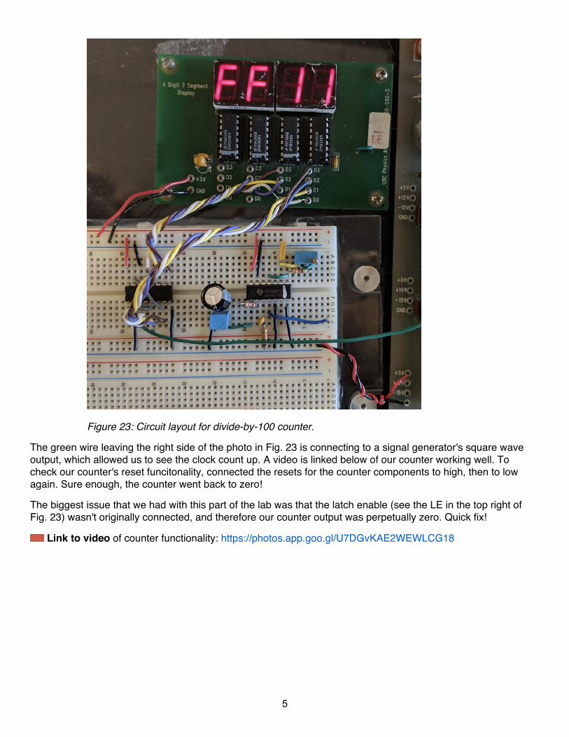
Figure 23: Circuit layout for divide-by-100 counter.
The green wire leaving the right side of the photo in Fig. 23 is connecting to a signal generator's square waveoutput, which allowed us to see the clock count up. A video is linked below of our counter working well. Tocheck our counter's reset funcitonality, connected the resets for the counter components to high, then to lowagain. Sure enough, the counter went back to zero!
The biggest issue that we had with this part of the lab was that the latch enable (see the LE in the top right ofFig. 23) wasn't originally connected, and therefore our counter output was perpetually zero. Quick fix!
Link to video of counter functionality: https://photos.app.goo.gl/U7DGvKAE2WEWLCG18
5
Experiment #6a: Analog-to-Digital Convertor
Part 3
Emma Gray, 36396166
Partner: Julia Rosenrauch
Table of Contents
Experiment #6a: Analog-to-Digital Convertor......................................................................................................... 1Part 3.......................................................................................................................................................................1
Emma Gray, 36396166.......................................................................................................................................1Partner: Julia Rosenrauch...................................................................................................................................13.4 Analog-to-Time Converter.............................................................................................................................13.5 Control Logic.................................................................................................................................................6
4. Integration of Components................................................................................................................................. 74.1 Circuit Signal Breakdown & Basic Relationships......................................................................................... 74.2 Written Description of Operation:................................................................................................................. 9
5. Conclusion.........................................................................................................................................................13
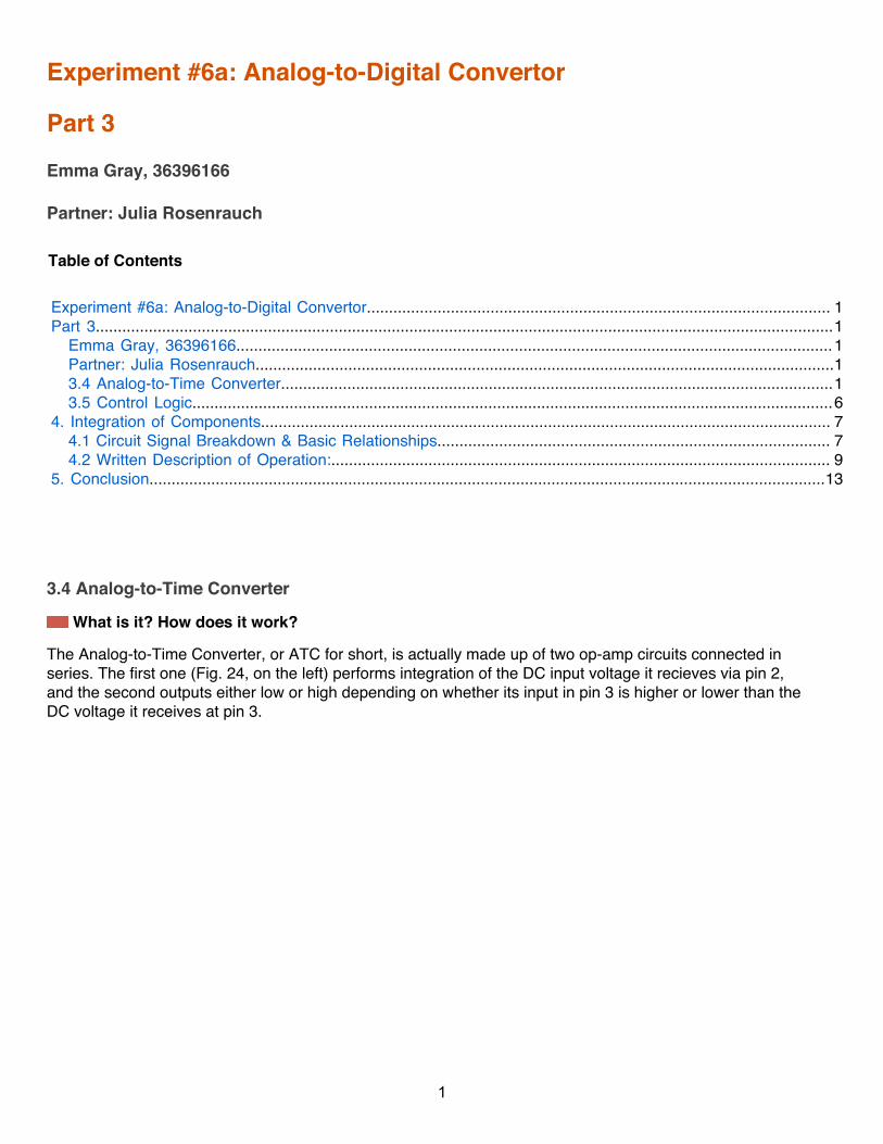
3.4 Analog-to-Time Converter
What is it? How does it work?
The Analog-to-Time Converter, or ATC for short, is actually made up of two op-amp circuits connected inseries. The first one (Fig. 24, on the left) performs integration of the DC input voltage it recieves via pin 2,and the second outputs either low or high depending on whether its input in pin 3 is higher or lower than theDC voltage it receives at pin 3.
1
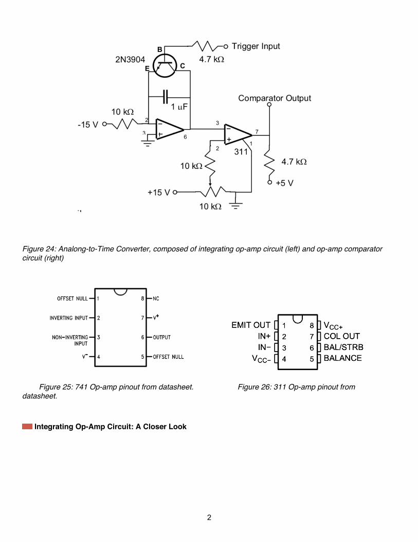
Figure 24: Analong-to-Time Converter, composed of integrating op-amp circuit (left) and op-amp comparatorcircuit (right)
Figure 25: 741 Op-amp pinout from datasheet. Figure 26: 311 Op-amp pinout fromdatasheet.
Integrating Op-Amp Circuit: A Closer Look
2
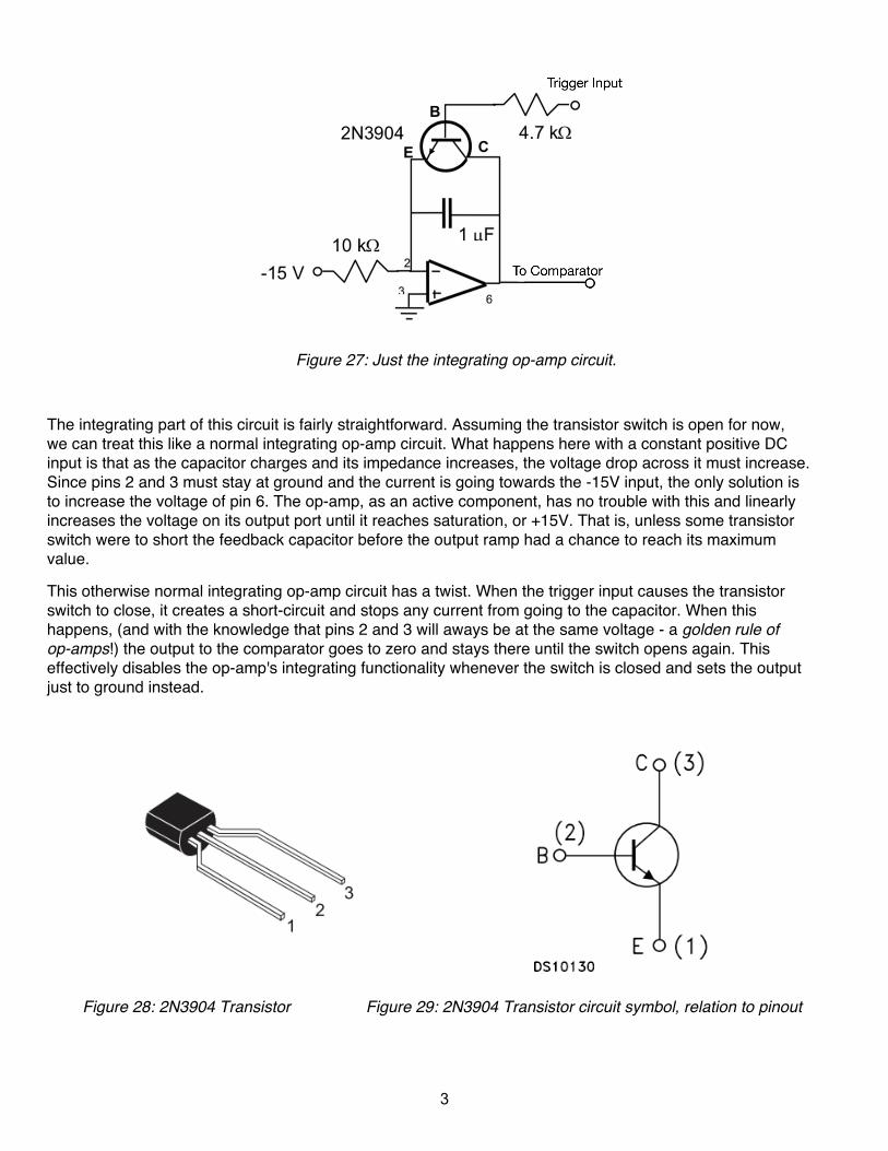
Figure 27: Just the integrating op-amp circuit.
The integrating part of this circuit is fairly straightforward. Assuming the transistor switch is open for now,we can treat this like a normal integrating op-amp circuit. What happens here with a constant positive DCinput is that as the capacitor charges and its impedance increases, the voltage drop across it must increase.Since pins 2 and 3 must stay at ground and the current is going towards the -15V input, the only solution isto increase the voltage of pin 6. The op-amp, as an active component, has no trouble with this and linearlyincreases the voltage on its output port until it reaches saturation, or +15V. That is, unless some transistorswitch were to short the feedback capacitor before the output ramp had a chance to reach its maximumvalue.
This otherwise normal integrating op-amp circuit has a twist. When the trigger input causes the transistorswitch to close, it creates a short-circuit and stops any current from going to the capacitor. When thishappens, (and with the knowledge that pins 2 and 3 will aways be at the same voltage - a golden rule ofop-amps!) the output to the comparator goes to zero and stays there until the switch opens again. Thiseffectively disables the op-amp's integrating functionality whenever the switch is closed and sets the outputjust to ground instead.
Figure 28: 2N3904 Transistor Figure 29: 2N3904 Transistor circuit symbol, relation to pinout
3
Op-Amp Comparator Circuit: A Closer Look
Figure 30: Just the comparator op-amp circuit.
This is an open loop op-amp, which means its outputs are always one of its two saturation modes (it'll alwaysbe trying to get its inputs to equal voltages, but there's no feedback so this isn't possible). When the voltageat pin 2 of this op-amp is fixed, and the voltage from the integrator circuit is higher than that, then the op-ampwill saturate towards -Vcc, or in this case, "low"/ground, to try to counterbalance it. Similarly, if the voltagefrom the integrator circuit is lower than the voltage at pin 2, it will saturate towards +Vcc and output high.
In order to test our ATC, we used a 100Hz, 5Vpp square wave with a 2.5V offset from the function generator.This was in place of our trigger pulse generator, with permission from the TAs. As expected, the comparatoroutputted high whenever the ramp was below its specified comparing voltage, and low whenever the rampexceeded it. This can be seen in the oscilloscope photo and the exported data below:
4
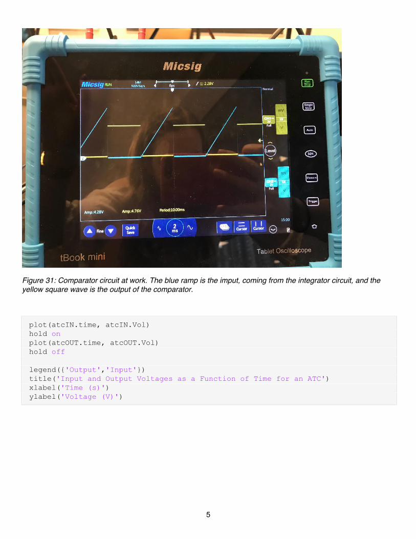
Figure 31: Comparator circuit at work. The blue ramp is the imput, coming from the integrator circuit, and theyellow square wave is the output of the comparator.
plot(atcIN.time, atcIN.Vol)hold on plot(atcOUT.time, atcOUT.Vol)hold off legend({'Output','Input'})title('Input and Output Voltages as a Function of Time for an ATC')xlabel('Time (s)')ylabel('Voltage (V)')
5
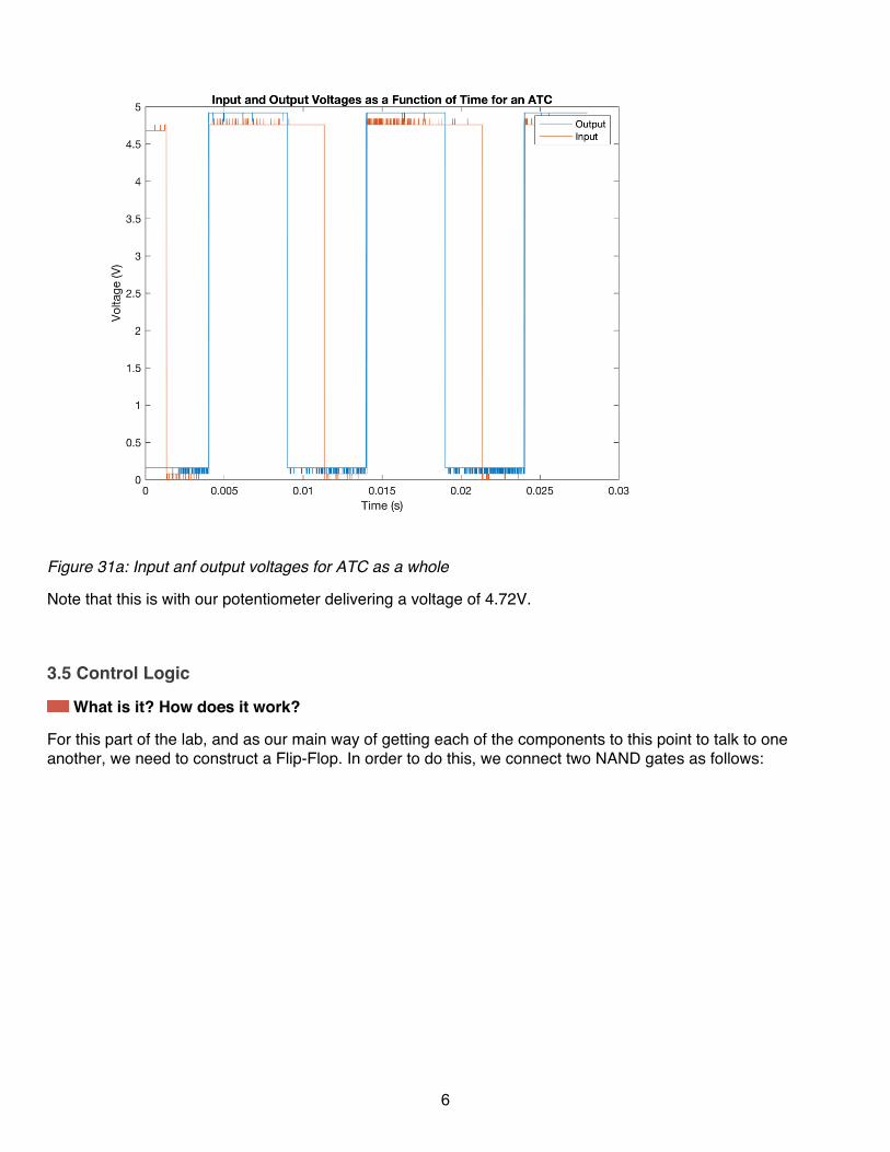
Figure 31a: Input anf output voltages for ATC as a whole
Note that this is with our potentiometer delivering a voltage of 4.72V.
3.5 Control Logic
What is it? How does it work?
For this part of the lab, and as our main way of getting each of the components to this point to talk to oneanother, we need to construct a Flip-Flop. In order to do this, we connect two NAND gates as follows:
6
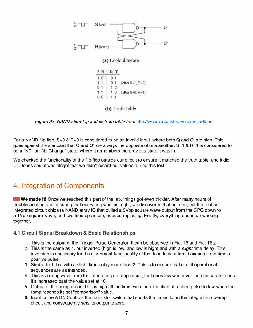
Figure 32: NAND Flip-Flop and its truth table from http://www.circuitstoday.com/flip-flops.
For a NAND flip-flop, S=0 & R=0 is considered to be an invalid input, where both Q and Q' are high. Thisgoes against the standard that Q and Q' are always the opposite of one another. S=1 & R=1 is considered tobe a "NC" or "No Change" state, where it remembers the previous state it was in.
We checked the funcitonality of the flip-flop outside our circuit to ensure it matched the truth table, and it did.Dr. Jones said it was alright that we didn't record our values during this test.
4. Integration of Components
We made it! Once we reached this part of the lab, things got even trickier. After many hours oftroubleshooting and ensuring that our wiring was just right, we discovered that not one, but three of ourintegrated circuit chips (a NAND array IC that pulled a 5Vpp square wave output from the CPG down toa 1Vpp square wave, and two fried op-amps), needed replacing. Finally, everything ended up workingtogether.
4.1 Circuit Signal Breakdown & Basic Relationships
1. This is the output of the Trigger Pulse Generator. It can be observed in Fig. 16 and Fig. 16a.2. This is the same as 1, but inverted (high is low, and low is high) and with a slight time delay. This
inversion is necessary for the clear/reset functionality of the decade counters, because it requires apositive pulse.
3. Similar to 1, but with a slight time delay more than 2. This is to ensure that circuit operationalsequences are as intended.
4. This is a ramp wave from the integrating op-amp circuit, that goes low whenever the comparator seesit's increased past the value set at 10.
5. Output of the comparator. This is high all the time, with the exception of a short pulse to low when theramp reaches its set "comparison" value.
6. Input to the ATC. Controls the transistor switch that shorts the capacitor in the integrating op-ampcircuit and consequently sets its output to zero.
7
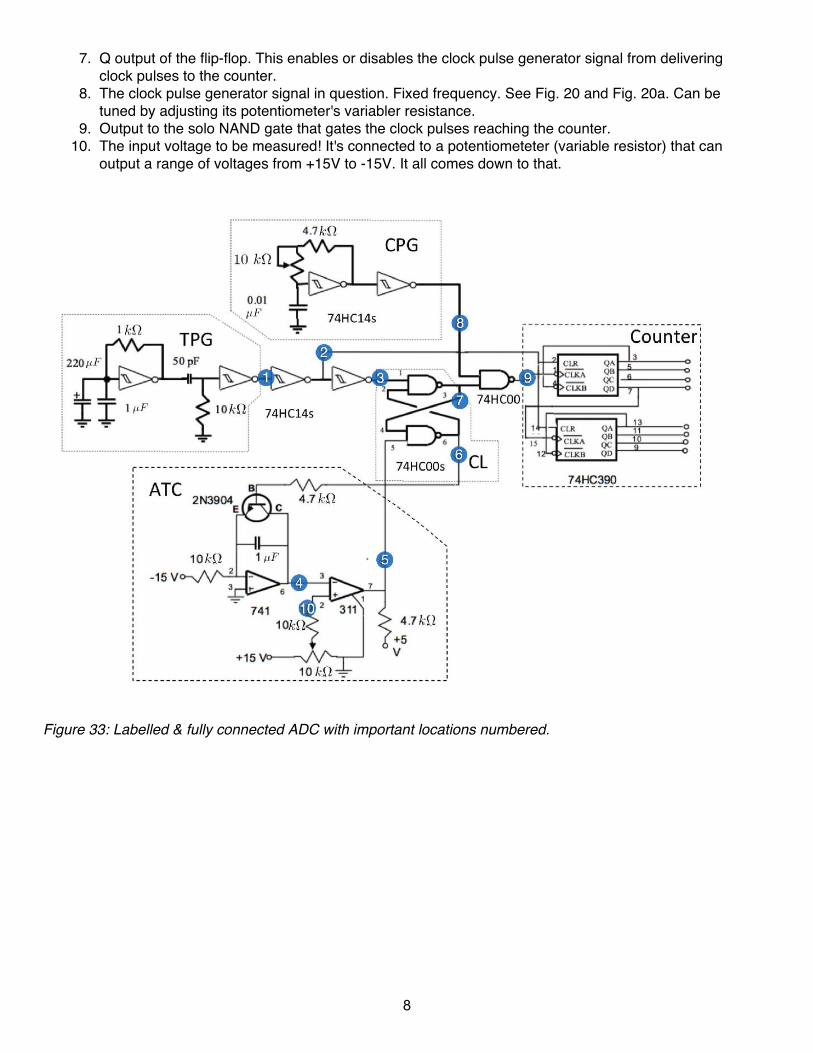
7. Q output of the flip-flop. This enables or disables the clock pulse generator signal from deliveringclock pulses to the counter.
8. The clock pulse generator signal in question. Fixed frequency. See Fig. 20 and Fig. 20a. Can betuned by adjusting its potentiometer's variabler resistance.
9. Output to the solo NAND gate that gates the clock pulses reaching the counter.10. The input voltage to be measured! It's connected to a potentiometeter (variable resistor) that can
output a range of voltages from +15V to -15V. It all comes down to that.
Figure 33: Labelled & fully connected ADC with important locations numbered.
8
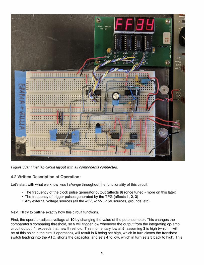
Figure 33a: Final lab circuit layout with all components connected.
4.2 Written Description of Operation:
Let's start with what we know won't change throughout the functionality of this circuit:
• The frequency of the clock pulse generator output (affects 8) (once tuned - more on this later)• The frequency of trigger pulses generated by the TPG (affects 1, 2, 3)• Any external voltage sources (all the +5V, +15V, -15V sources, grounds, etc)
Next, I'll try to outline exactly how this circuit functions.
First, the operator adjusts voltage at 10 by changing the value of the potentiometer. This changes thecomparator's comparing threshold, so 5 will trigger low whenever the output from the integrating op-ampcircuit output, 4, exceeds that new threshold. This momentary low at 5, assuming 3 is high (which it willbe at this point in the circuit operation), will result in 6 being set high, which in turn closes the transistorswitch leading into the ATC, shorts the capacitor, and sets 4 to low, which in turn sets 5 back to high. This
9
all happens so quickly that 5 just looks like a quick pulse low from an otherwise high signal. That's how thelower part of the circuit works.
The TPG is what triggers the ramp wave in the first place. When it goes low, 3 also goes low (slightly later)and that in turn sets 6 low, so that the transistor switch opens, the capacitor is no longer shorted and theintegrating op-amp's integrating functionality is restored.
Lastly, we have counting. When 7 is low, no matter what the clock pulse at 8 is, the output to the NAND gateto the right of the flip-flop is set to high. 7 is only high from when 1 pulses low from high to when 5 pulseslow from high - this also explains why the ramps go for the duration they do before being set to zero - thanksto the "remember" functionality of the flip-flop when both inputs are high, we get a window where thesecomponents behave a certain way, and the rest of the time they behave another way.
When 7 is high and 8's clock pulse triggers back and forth from low to high, the output to the NAND suddenlylooks like an inverted version of the CPG signal. Since the counter's clock is triggered on rising edges, thatsquare wave NAND output starts making the counter count.
It's also worth noting that 1 pulsing low on 7's rising edge results in 2 pulsing high (since they're connectedby an inverter), resetting the counter right before it starts counting each time. This allows us to store anddisplay the last counted number until the next time the counting starts.
The counting all happens so fast that to us, it appears as though the 7-segment display just refreshes withnew numbers right after each other.
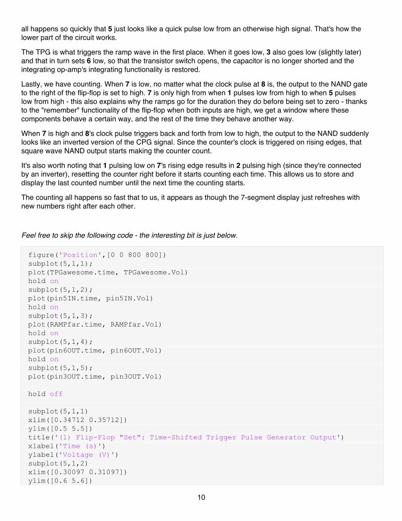
Feel free to skip the following code - the interesting bit is just below.
figure('Position',[0 0 800 800])subplot(5,1,1);plot(TPGawesome.time, TPGawesome.Vol)hold onsubplot(5,1,2);plot(pin5IN.time, pin5IN.Vol)hold onsubplot(5,1,3);plot(RAMPfar.time, RAMPfar.Vol)hold onsubplot(5,1,4);plot(pin6OUT.time, pin6OUT.Vol)hold onsubplot(5,1,5);plot(pin3OUT.time, pin3OUT.Vol) hold off subplot(5,1,1)xlim([0.34712 0.35712])ylim([0.5 5.5])title('(1) Flip-Flop "Set": Time-Shifted Trigger Pulse Generator Output')xlabel('Time (s)')ylabel('Voltage (V)')subplot(5,1,2)xlim([0.30097 0.31097])ylim([0.6 5.6])
10
title('(5) Flip-Flop "Reset": ATC Comparator Output')xlabel('Time (s)')ylabel('Voltage (V)')subplot(5,1,3)xlim([0.19000 0.20000])ylim([-0.2 4.8])title('(4) Ramp Output from Integrating Op-Amp')xlabel('Time (s)')ylabel('Voltage (V)')subplot(5,1,4)xlim([0.22154 0.23154])ylim([-0.4 4.6])title('(6) Flip-Flop Q'': Input to ATC')xlabel('Time (s)')ylabel('Voltage (V)')subplot(5,1,5)xlim([0.18774 0.19774])ylim([-0.2 4.8])title('(7) Flip-Flop Q: Input to Counter Clock NAND Gate')xlabel('Time (s)')ylabel('Voltage (V)')
11
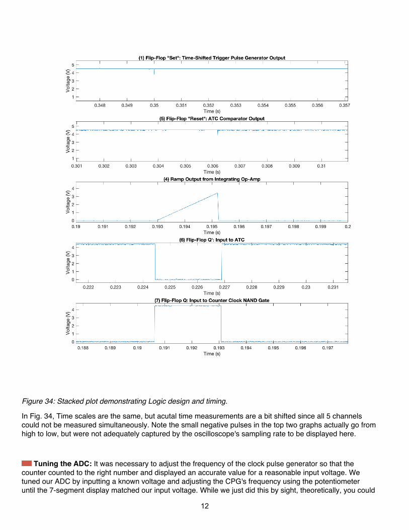
Figure 34: Stacked plot demonstrating Logic design and timing.
In Fig. 34, Time scales are the same, but acutal time measurements are a bit shifted since all 5 channelscould not be measured simultaneously. Note the small negative pulses in the top two graphs actually go fromhigh to low, but were not adequately captured by the oscilloscope's sampling rate to be displayed here.
Tuning the ADC: It was necessary to adjust the frequency of the clock pulse generator so that thecounter counted to the right number and displayed an accurate value for a reasonable input voltage. Wetuned our ADC by inputting a known voltage and adjusting the CPG's frequency using the potentiometeruntil the 7-segment display matched our input voltage. While we just did this by sight, theoretically, you could
12
intentionally choose the frequency to be equal to ten times the slope of the ramp wave, such that it countsfrom 0 to 10*Vin (so you can get one decimal place in your measurement) over the course of one rampperiod.
For example, the ramp wave in Fig. 34 has a period of approximately 0.00225s. As the ramp cuts off ataround 3.5V, you'd want the clock pulse to count to 35 in 0.00225 seconds, and therefore the frequencyof the clock pulse in this case should be 35/0.00225s, or approximately 15.5kHz. This is just a rough run-through with numbers in the event that we didn't have the chance to tune it in person (thankfully, we did). Therequired tuning of the ADC changes based on the slope of the ramp, which will be constant unless the ATCcapacitor's value is changed.
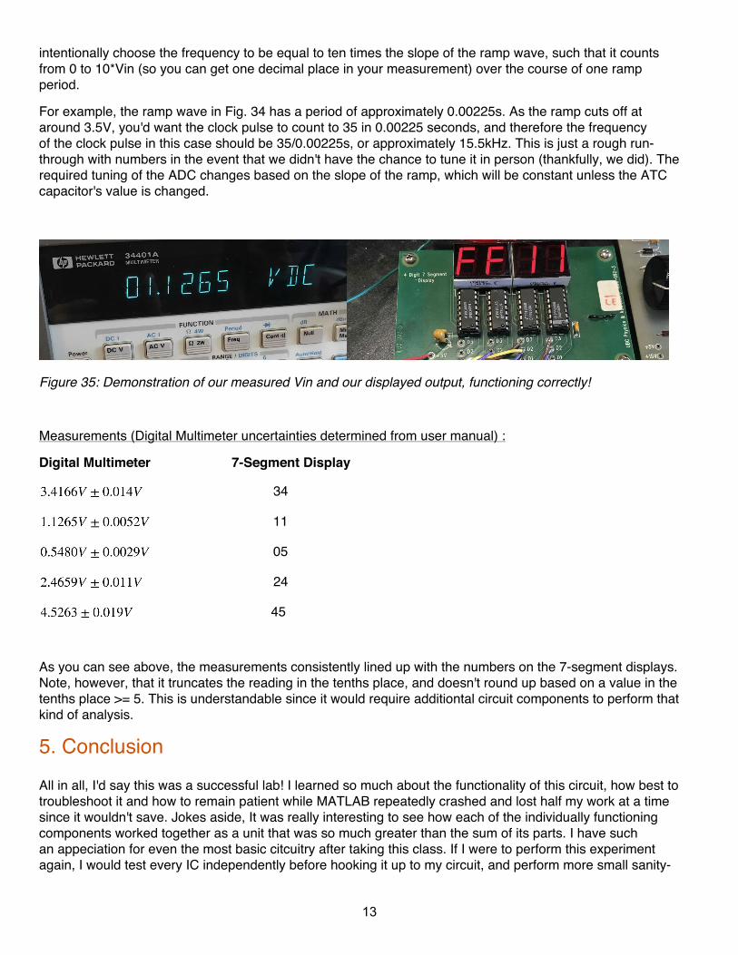
Figure 35: Demonstration of our measured Vin and our displayed output, functioning correctly!
Measurements (Digital Multimeter uncertainties determined from user manual) :
Digital Multimeter 7-Segment Display
34
11
05
24
45
As you can see above, the measurements consistently lined up with the numbers on the 7-segment displays.Note, however, that it truncates the reading in the tenths place, and doesn't round up based on a value in thetenths place >= 5. This is understandable since it would require additiontal circuit components to perform thatkind of analysis.
5. ConclusionAll in all, I'd say this was a successful lab! I learned so much about the functionality of this circuit, how best totroubleshoot it and how to remain patient while MATLAB repeatedly crashed and lost half my work at a timesince it wouldn't save. Jokes aside, It was really interesting to see how each of the individually functioningcomponents worked together as a unit that was so much greater than the sum of its parts. I have suchan appeciation for even the most basic citcuitry after taking this class. If I were to perform this experimentagain, I would test every IC independently before hooking it up to my circuit, and perform more small sanity-
13

checking tests as I go to ensure I'm not looking for the inevitible bugs in the wrong places. Thanks for a greatsemester!
14
Related Documents