FMCW system receiver front end 1 FMCW radar receiver front-end design THESIS submitted in partial fulfillment of the requirements for the degree of MASTER OF SCIENCE in ELECTRONIC ENGINEERING (MICROELECTRONICS) by Yanfei Mao born in Zhejiang, China Supervisors Dr. Ing Leo de Vreede Prof. John Long Mr Cicero Vaucher

Welcome message from author
This document is posted to help you gain knowledge. Please leave a comment to let me know what you think about it! Share it to your friends and learn new things together.
Transcript

FMCW system receiver front end
1
FMCW radar receiver front-end design
THESIS
submitted in partial fulfillment of the requirements for the degree of MASTER OF SCIENCE
in
ELECTRONIC ENGINEERING (MICROELECTRONICS)
by Yanfei Mao
born in Zhejiang, China Supervisors
Dr. Ing Leo de Vreede Prof. John Long
Mr Cicero Vaucher

FMCW system receiver front end
2
FMCW radar receiver front-end design
Author: Yanfei Mao Student ID: 1389211 Email: [email protected]
Abstract
The main focus of this thesis is the design a receiver frontend for FMCW radar applications. In these systems, the increasing requirements on detection resolution, points towards the use of higher frequencies. In view of this, frequencies at W-band are very attractive due to the potential of high spatial resolution, while chip size and antennas can be made more compact. However, to realize such a high performance FMCW radar system, a W-band high bandwidth LNA-mixer chain needs to be developed in a high-end integration technology. Key design parameters are low noise, high conversion gain and linearity, and above all a large operating bandwidth. Due to the application requirements in this project, high isolation between received signal and the down converting LO signal needs to be established. System considerations have been given in support of understanding and defining the LNA-mixer specifications.
Key Words: 94GHz, direct conversion architecture, LNA mixer chain Thesis Committee: Chair: University Supervisor: Dr. Ing. Leo de Vreede, Faculty EEMCS, TU Delft Company Supervisor: Committee Member:

FMCW system receiver front end
3
Acknowledgement
The project started from May 2008 and has last for 10 months. I would like to express my gratitude to all the colleagues for their help.
First of all, I would like to thank my supervisor Dr. Leo de Vreede for granting me the opportunity to carry research upon this interesting topic. Discussions with him always illuminate my way to next step. It is his guidance that encourages me to complete this project. I’m so glad that I have such intelligent and kind supervisor.
Secondly, I would like to thank my mentor from NXP, Mr Cicero Vaucher. Thanks for his support and suggestions on my work.
Thirdly, I would like to say “thanks” to Prof. John Long, for supporting on libraries and tape-out, and all members of HiTeC Group, especially Akhnoukh,A. Atef, who gave me lots help on cadence and layout and Marco Pelk, Han Yan, Cong Huang, who are so kind to give me suggestions and help me to solve simulation problems. Also many thanks to my colleagues, Sandeep, Nan Li, Lai Jiang and Tao Zhang, for their suggestions upon my work and happiness they bring about.
Finally, I appreciate all my friends and my family. Your love and understanding encourage me to finish my Master program and to overcome the difficulties I faced.

FMCW system receiver front end
4
TABLE OF CONTENTS
1. Introduction………………………………………………………………………………………6 1.1 FMCW System introduction…………………………………………………………………6
1.2 Receiver front-end architecture and specification……………………………………………9 1.2.1 Receiver front-end architecture selection………………………………………………. 9 1.2.2 Receiver front-end specification……………………………………………………….10 2. General consideration and specification of LNA……………………………………………….13 2.1 Two-port power gains……………………………………………………………………….13 2.2 Noise figure…………………………………………………………………………………14 2.3 Stability……………………………………………………………………………………..14 2.4 Linearity…………………………………………………………………………………….14 2.5 Smith Chart and impedance matching……………………………………………………...18 2.6 The 180o hybrid…………………………………………………………………………….19 3. Design of two-stage wideband LNA…………………………………………………………...21 3.1 High frequency transistor model……………………………………………………………21
3.1.1 parasitic capacitances…………………………………………………………………..21 3.1.2 parasitic resistances…………………………………………………………………….22
3.2 Circuit topology selection…………………………………………………………………..23 3.2.1 the noise analysis of the common-emitter……………………………………………..23 3.2.2 the noise analysis of the common-base configuration…………………………………27 3.2.3 the noise analysis of the cascode stage………………………………………………...29
3.3 Design process……………………………………………………………………………...31 3.3.1 the biasing of the transistor…………………………………………………………….31
3.4 different circuit topologies…………………………………………………….. ..…………35 3.4.1.1 cascaded cascode LNA…….………………………………………………………...35 3.4.1.2 wideband low Q interstage matching LNA……………………………………….…41 3.4.2 inductive degeneration cascode LNA………………………………………………….43 3.4.3 common base input two stage LNA……………………………………………………46
3.5 comparison of different topologies of LNA………………………………………………...49 4. Specification and design of mixers……………………………………………………………..51 4.1 Specifications of mixers…………………………………………………………………….51 4.1.1 conversion gain……………………………………………………………………….51 4.1.2 noise figure……………………………………………………………………………51 4.1.3 isolation……………………………………………………………………………….52 4.1.4 linearity……………………………………………………………………………….52 4.2 noise analysis of double balanced mixer……………………………………………………53 4.3 design process of the mixer…………………………………………………………………55 4.3.1 biasing of the transistors……………………………………………………………...55 4.3.2 inductive degeneration………………………………………………………………..56 4.3.3 current bleeding……………………………………………………………………….57 4.3.4 the mixer performance………………………………………………………………..58
4.3.5 The mixer performance comparison before and after noise optimization……………..60 4.3.6 buffers………………………………………………………………………………….60

FMCW system receiver front end
5
5. Overall performance and verification……………………………………………………..……63 5.1 overall performance…………………………………………………………………….......63 5.2 system verification upon noise figure………………………………………………………67
6. More upon LNA………………………………………………………………………………...69 6.1 biasing circuits for the LNA...……………………………………………………….…......69 6.2 decoupling…………………………………………………………………………….…….71 6.3 process and temperature variation………………………………………………………….76 6.4 layout for LNA and mixer………………………………………………………………….78
7. Conclusion……………………………………………………………………………………...81 7.1 conclusions………………………………………………………………………………….81 7.2 further discussion…………………………………………………………………………...81 7.2.1 single side band mixer implementation………………………………………………..81 Reference…………………………………………………………………………………………..85
FMCW system receiver front end
6
1 FMCW System introduction and receiver
front end specification
In this chapter, firstly background upon FMCW radar system is given; then two possible architectures upon receiver front end are discussed and compared; and finally system specification of the front end is discussed and given.
1.1 FMCW System introduction[1]
Low-cost short range radar systems can be applied in various fields like security, medical imaging, logistics, quality control etc in future. In various applications, with increasing requirements on the radar detection resolution, the use of higher frequencies and more advanced integration technology is mandatory. Signal frequencies at W-band are very attractive due to their high spatial resolution, the resulting compact chip size and small antenna dimensions.[2-4] Since different radar applications have also different requirements/conditions on resolution, object distance and medium attenuation, various radar principles have been proposed, ranging from impulse, CW, FM-CW radar systems, each with its own specific system requirements. Various challenges are found when applying these concepts at (sub)mmwave frequencies for improved resolution and form factor, like integration of the system functions like antenna, signal up and down conversion, signal generation, signal phase or time delay control and signal combing, isolation between transmit and receive, system bandwidth and ultra-fast data acquisition. Among these different kinds of systems, the FM-CW system is often favored over others.
Firstly, FM-CW radar system concept is less demanding in terms of transmit power. Since FM-CW systems continuously transmit power (compared to other systems like pulse systems), the required peak transmit power is lower, while still resulting in a much better signal-to-noise ratio. Secondly, the detection bandwidth in the data acquisition is limited; this reduces the noise bandwidth considerably and results in a better signal-to-noise ratio. It also relaxes the speed requirements on the data acquisition.
There are also some drawbacks on FM-CW systems, which can complicate their implementation. Firstly, the isolation requirement of transmit to receive path in order to avoid receiver saturation. This requires physical separation or isolation enhancements of transmit and receive path. Secondly, in signal generation, signals with low phase noise in combination with fast frequency sweeping should be generated. Thirdly, the antenna needs to be wideband, since we sweep the frequency for the object detection over a large range. When FM-CW is applied in combination with a frequency scanning array the observation angle becomes also a function of transmit frequency, this complicates the signal processing needed for the radar imaging.
Figure 1.1 shows the FM-CW radar principle. [5] Figure 1.2 shows the modulation scheme for the FM-CW radar, a transmit signal, and return from a point target. The two-way travel time is τ, the bandwidth of the transmit signal is B, the sweep time is T, and the period is TM. At any instant in time, the transmit and receive signals are multiplied by a mixer. Since multiplying two

FMCW system receiver front end
7
sinusoidal signals together results in a sum and difference terms, after low pass filtering, we are left with only the difference term. The frequency of this signal is given by fb , the beat frequency. Intended beat frequency in the work plan range from DC to 500MHz. Thus in this project, 500MHz is the output IF frequency throughout the design.
An expression for the beat frequency can easily be found. Using similar triangles and rearranging terms, we obtain the following expression:
bf BTτ
= (equation 1.1)
Since the beat frequency signal is time limited to T seconds, when only one target exists, its
spectrum will be a sinc function centered at bf , and the first zero crossing will occur at 1
2f
T= .
[26]When multiple targets exist, the result will be a superposition of many beat frequencies. In the
frequency domain, two targets’ beat frequencies can be as close together as 1T
. Since from (1.1)
we have: T bf
BΔ
Δτ = (equation 1.2)
Plugging in 1TbfΔ = , we have
1Δτ =
Β. Hence, the minimum resolvable separation in
time between two targets is inversely proportional to the bandwidth. The two way time to a target, τ, and the range to a target, R, are related by the following formula:
cR τ=2
(equation 1.3)
so the range of detection and range resolution is given by: c c bf TR τ
= =2 2 Β
(equation 1.4)
1c* *cc cbTf T TR ΔΔτ
Δ = = = =2 2Β 2Β 2Β
(equation 1.5)
According to equation 1.4, since the beat frequency is proportional to τ, and τ is proportional to range, knowledge of the beat frequency of any target entails knowledge of the range of that target. With many targets, we can separate them by taking the Fourier Transform of the received signal, and determine range through frequency.
Our intended center working frequency for the FM-CW system is 94GHz. To achieve high detection resolution, the bandwidth of our systems need to be maximized. An increase in frequency will help to achieve the desired resolution. Since the bandwidth of antennas and microwave circuits is typically restricted to 20-30% relative bandwidth with respect of center design frequency, in this design, the bandwidth for the system is between 84GHz-104GHz, a range resolution can be 7.5mm with 20GHz bandwidth.
From the radar equation, the amount of power returning to the receiver antenna is as follows,
( )
4
r 2 2 2P
4t t r
t r
PG A FR Rσ
=π
(equation 1.6)

FMCW system receiver front end
8
From this equation, the received power declines as the fourth power of the range, this means that the reflected power from distant targets will be very, very small. Typical received signal power will be around -150dBm to -30dBm. In addition in a real-world situation, also the path loss effects should also be considered, and the received power will be even smaller.
Fig. 1.1 The FM-CW radar principle
Figure 1.2 modulation scheme for FM-CW radar
Figure 1.3 DDS based FM-CW radar system
Figure 1.3 shows a DDS (Direct Digital Signal generation) based FM-CW radar system

FMCW system receiver front end
9
implementation (assuming a single antenna). 8× active frequency multipliers are utilized to create the high bandwidth 84-104 GHz linear sweeping signals. In the signal down conversion path, a high bandwidth 84-104 GHz LNA followed by an active mixer is utilized to obtain the
difference frequency bf .
1.2 Receiver front-end architecture and specification
1.2.1 Receiver front-end architecture homodyne receiver[6]
If the RF spectrum is translated to the baseband in the first downconversion, then this type of receiver is called “homodyne”, “direct conversion”, or “zero-IF” architecture, as shown in figure 1.4.
Figure 1.4 simple homodyne receiver
Using a homodyne receiver architecture, the difference frequency between the transmitted
signal and received signal can be easily obtained if the frequency swept transmit signal is used for the LO down conversion. Consequently this architecture is the preferred solution.
Nevertheless, this type of receiver architecture in the application of this project entails some problems ike image problems, DC offsets, even-order distortion, and flicker noise. All these issues will be discussed below.
The image problem Usually, the homodyne receiver shown in figure 1.6 operates only with double-sided signals,
which overlap the positive and negative parts of the input spectrum. Consequently, the image
frequency problem is circumvented because IF 0ω = . As a result, no image filter is required.
Nevertheless, in this project, the transmitted and the received frequencies are not the same, thus the image frequency problem is an issue in this case. Strictly speaking, the direct conversion here is no longer strictly defined as a homodyne receiver. As result due to the image frequency problem, the overall noise figure of the down conversion chain will be 3 dB higher. We will discuss this in Chapter 5 in detail.
DC offsets In a homodyne topology, the downconverted band extends to zero frequency, so an offset
voltage can corrupt the signal and more importantly, saturate the following stages. Usually, there are two kinds of DC offset related phenomenon. Firstly, LO leakage can cause
DC offset. This occurs when the isolation between the LO port and the inputs of the mixer and the

FMCW system receiver front end
10
LNA is not infinite; in this case a finite amount of feed through exists from the LO port to input of LNA and mixer due to the capacitive and substrate coupling, or bond wire coupling. The leakage signal appearing at the inputs of the LNA and mixer is mixed with the LO signal, providing a DC component at the output of the mixer. This phenomenon is called self mixing. Another phenomenon arises if a large interferer leaks from the LNA or mixer input to the LO ports and is multiplied by itself. The principle is similar with self mixing.
The DC offset is exacerbated if self mixing varies with time. Usually, in communication systems DC offsets problem can be solved by “DC free coding”,
in which the baseband signal in the transmitter can be encoded such that after modulation and downconversion, it contains little energy near DC. Another technique is to exploit the idle time intervals in digital wireless standards to carry out offset cancellation.
DC offsets is much less severe in heterodyne architectures. In this project, DC offsets mainly arises from two reasons. Firstly, self mixing or LO leakage,
due to capacitive coupling, substrate coupling, LO leakage at the LNA or when the mixer input is mixed with the LO signal, providing a DC component at the output of the mixer.
In a dc-coupled mixer output buffer, DC offsets will cause reduced dynamic range of the data acquisition. Careful layout, high LNA reverse isolation, high LO-RF isolation will help to reduce the DC offsets.
Even-order distortion Even-order nonlinearity becomes problematic in homodyne downconversion systems. When
two strong interferers close to the channel of interest experience an even-order nonlinearity they will generate a low-frequency beat. Because mixers exhibit a finite direct feedthrough from the RF input to the IF output due to asymmetry in the mixing core, the low-frequency beat will appear in the IF port. Besides, the mixer RF port may also suffer from even-order distortion, requiring special attention in the design.
In this project, because the LNA is single-ended, thus careful layout of mixer is required to reduce the direct feed through and prevent even-order distortion of LNA appearing at the mixer IF output, this requires the optimization of the IIP2 of the mixer. However, it is expected that interfering signals are mostly originating from the radar system itself (e.g. by bad isolation or close by object reflections) than from other unknown jamming sources.
Flicker noise Since the down-converted spectrum extends to zero frequency, the 1/f noise of devices
substantially corrupts the signal, especially for the dc coupled mixer output, and for the short range radar detection when the output signal is close to the dc component.
Relative high gain in the RF range is preferred to reduce the interferences of flicker noise, and noise contributions of stages that follow the mixer. Note that one can reduce the Flicker noise by using very large devices in the IF part of the circuitry.
1.2.2 Receiver front-end specification
For receiver front end, typically around 30dB gain [6] should be provided by the combination of LNA and mixer. Considering a working frequency as high as 94GHz, a noise figure around 10dB for the overall chain is considered tolerable.

FMCW system receiver front end
11
The bandwidth of difference frequency bf is within 500MHz. Accordingly, the noise floor
can be calculated as follows:
9
174 10log = 174 10 10log10 = 74
F dBm NF B= − + +
− + +−
(equation 1.7)
Nevertheless, applying a FFT after waveform acquisition will change the effective noise floor. The system will employs an fast A/D converter in order to acquire the IF signals and to shift from the analog to the digital domain. Proposed A/D converters employed are 100MS/s NI PXI-5122 14-bit digitizers,[17] their theoretical dynamic range can be calculated from the number of bits and the input voltage range. For an input range of 400 mV peak to peak, the maximum power level that can be measured with a 50ohm input impedance is:
( ) ( ) ( )2 22
maxmaxmax
/ 2 200 / 2( ) 10log 10log 10log 33.9
50 50 50PeakRMS
V mVVP dB dBW= = = = −
Ω Ω Ω(equation 1.8)
The lowest power that can be measured due to the quantization noise of the digitizer is:
( ) ( )22 14
min
400 /(2 ) 2( ) 10log 10log 112.2
50 50RMSqnoise mVV
P dB dBW= = = −Ω Ω
(equation 1.9) yielding a dynamic range of:
max min( ) ( ) 78.3DR P dB P dB dB= − = (equation 1.10)
This is the dynamic range in absence of noise sources other than the quantization. In reality, as specified on the datasheet, the DAQ card will have an intrinsic rms noise of 92μV, hence:
( ) ( )2 2
min
92( ) 10log 10log 97.7
50 50RMSqnoiseV uV
P dB dBW= = = −Ω Ω
(equation 1.11) Thus the limit in dynamic range due to the total noise is:
max min( ) ( ) 63.7DR P dB P dB dB= − = (equation 1.12)
In these applications, the signal of interest occupies a bandwidth, BW, smaller then than the maximum Nyquist bandwidth. If digital filtering is used to filter out noise components outside the bandwidth, then a correction factor, called process gain, must be included to account for the resulting increase in the signal to noise ratio. Thus
max min( ) ( ) 10log2
sfDR P dB P dBBW
⎛ ⎞= − + ⎜ ⎟⎝ ⎠
(equation 1.13)
Performing an M-point FFT over the acquired waveform to extract information about a particular frequency component, is equivalent to digitally filter the signal with a bandwidth equal to the frequency resolution of the FFT, that is fS/M. Therefore the dynamic range due to the

FMCW system receiver front end
12
discrete Fourier transform is:
max min( ) ( ) 10log2MDR P dB P dB ⎛ ⎞= − + ⎜ ⎟
⎝ ⎠ (equation 1.14)
According to datasheet, the digitizers can acquire 16 million samples per channel, that would
be 160 ms time period. If we choose 2 secMT m= , so 1 secT m= , then
61 *16 0.1*10160
M = = (equation 1.15)
So now the dynamic range becomes
max min( ) ( ) 10log2MDR P dB P dB ⎛ ⎞= − + ⎜ ⎟
⎝ ⎠ (equation 1.16)
Time-domain averaging can also increase the dynamic range. It attenuates asynchronous noise sources by averaging timedomain waveforms from multiple triggers. The signal bandwidth is not affected. The signal must be periodic to take advantage of this type of averaging. Noise variance is reduced by a factor equal to the number of averages. In terms of decibels, time domain
averaging reduces the noise floor by 10*log( )avgN , where avgN is the number of averages.
Dynamic range becomes:
max min( ) ( ) 10log 10*log( )2 avgMDR P dB P dB N⎛ ⎞= − + +⎜ ⎟
⎝ ⎠ (equation 1.17)
If 4avgN = , now the dynamic range becomes:
51063.7 10log 10*log(4) 116.72
DR dB⎛ ⎞
= + + =⎜ ⎟⎝ ⎠
(equation 1.18)
In order to adapt the large dynamic range of the input signal (roughly estimated -100dBm to -30dBm), and adapt to the maximum ADC input range, a VGA with variable gain 0-70dB is suggested to be inserted between the RF front end and the ADC. [22]
Lastly, from the application of the frontend, due to the small power of the input signal, gain is considered more important than linearity, nevertheless, insertion of VGA releases the gain requirement of the frontend a bit, while linearity should also be considered.
Therefore, the overall requirement of the RF frontend LNA-mixer chain is that low noise figure, high gain of LNA should be designed while maintaining suitable linearity for mixer.

FMCW system receiver front end
13
2 General consideration and specification of
LNA
The main function of the LNA is to provide enough gain to overcome the noise of subsequent stages (such as a mixer). Aside from providing this gain, while adding as little noise as possible, an LNA should accommodate large signals without distortion, and it must also present a specific impedance, such as 50 Ohm, to the receiving antenna. Thus a number of considerations govern the design of low-noise amplifiers: noise figure, linearity, gain, input and output return loss, reverse isolation, stability factor and so on. Following are some detailed discussion of these considerations and specification.
2.1 two-port power gains[7]
Consider an arbitrary two-port network [S] connected to source and load impedances Zs and ZL, respectively, we will derive expressions for three types of power gain in terms of the S
parameters of the two-port network and the reflection coefficients, SΓ and LΓ , of the source
and load.
Transducer power gain=GT= L avsP P is the ratio of the power delivered to the load to the
power available from the source. This quantity depends on both Zs and ZL. The reflection coefficient seen looking toward the load is
L oL
L o
Z ZZ Z
−Γ =
+ (equation 2.1)
The reflection coefficient seen looking toward the source is
S oS
S o
Z ZZ Z
−Γ =
+ (equation 2.2)
Transducer power gain: 2 2 2
212 2
22
(1 )(1 )1 1
S LLT
avs in s L
SPGP S
− Γ − Γ= =
−Γ Γ − Γ (equation 2.3)
A special case of the transducer power gain occurs when both the input and output are
perfectly matched. Then 0L SΓ = Γ = , and
221TG S= (equation 2.4)

FMCW system receiver front end
14
2.2 Noise figure
The most commonly accepted definition for noise figure is
in
out
SNRnoise figure=SNR
i i
o o
S NS N
= (equation 2.5)
iS , iN are the input signal and noise powers, and oS oN are the output signal and noise
powers. By definition, the input noise power is assumed to be the noise power resulting from a
matched resistor at 290oT K= , that is i oN kT B= .
Consider the cascade of m components, having gains G1, G2, Gm, noise figure NF1, NF2, NFm. The NF of each stage is calculated with respect to the source impedance driving that stage. The overall noise figure can be determined by
21
1 1 2
111 1 .... mcas
NFNFF NFG G G
−−= + − + + (equation 2.6)
2.3 Stability
There are two types of stability:
Unconditional stability: the network is unconditionally stable if 1inΓ < and 1outΓ < for
all passive source and load impedances.
Conditional stability: the network is conditionally stable if 1inΓ < and 1outΓ < only for
a certain range of passive source and load impedances.
2.4 linearity
For a simple CE stage, the voltage transfer of a CE stage is given as
exp 1INOUT CC C C CC C S
T
VV V R I V R IV
⎡ ⎤⎛ ⎞= − = − −⎢ ⎥⎜ ⎟
⎝ ⎠⎣ ⎦ (equation 2.7)

FMCW system receiver front end
15
Figure 4.1 CE stage
We can approximate this by a Taylor series expansion
( ) ( ) ( ) ( )2 31 2 3 ...y t a x t a x t a x t= + + + (equation 2.8)
With the coefficients na given by
( )01!
n
n n
d y Xa
n dx= (equation 2.9)
For a differential pair:
Figure 4.2 differential pair
The voltage transfer of the differential pair can be written:
tanh2
INOUT C EE
T
VV R IV
⎛ ⎞= ⎜ ⎟
⎝ ⎠ (equation 2.10)
Consequently the Taylor coefficients of the differential pair are :
1 2EE C
T
I RaV
= (equation 2.11)
FMCW system receiver front end
16
2 0a = (equation 2.12)
3 324EE C
T
I RaV
= − (equation 2.13)
Since the differential pair has an odd function, all na are 0 for even n.
Figure 4.3 1dB compression point
The 1dB compression point is found where the gain becomes 1dB smaller than the small signal gain. The dynamic range is defined as the margin between the minimal detectable power
( ,x mdsP ) and the 1dB compression point.
Assuming that the minimum detectable input level is X decibels above the thermal noise, we can write for the lowest detectable input level
, 174 10log( ) ( ) ( )i mdsP dBm B F dB X dB= − + + + (Equation 2.14)
And for the corresponding output level
, 174 10log( ) ( ) ( ) ( )o mds AP dBm B F dB X dB G dB= − + + + + (Equation 2.15)
The dynamic range of the amplifier is can be defined by the 1dB compression point,
,1 ,_ o dB o mdsDynamic range P P= − (Equation 2.16)
Note that the above definition for the dynamic range only took into account the limits of the noise floor and the gain compression, however, the constrains of the intermodulation products should also be considered.
Virtual crossings of fundamental with the intermodulation products is a measure for the achieved linearity. Intercept points for the CE stage

FMCW system receiver front end
17
122CE
T
AIMV
= (Equation 2.17)
2
2
138CE
T
AIMV
= (Equation 2.18)
2 2CE TIIP V= (Equation 2.19)
3 8CE TIIP V= (Equation 2.20)
Intercept points for the differential stage
2 0DPIM = (Equation 2.21)
2
2
1316DP
T
AIMV
= (Equation 2.22)
2DPIIP = ∞ (Equation 2.23)
3 4DP TIIP V= (Equation 2.24)
When considering the limitation of the IM3 products, the spur-free dynamic range is a more appropriate figure of Merit than the dynamic range, since it gives the ratio of the maximum input level that the circuit can tolerate to the minimum input level, with intermodulation products not exceeding this minimum level.
Figure 4.5 Spurious free dynamic range
( )323 IIPSFDR P F= − (equation 2.25)
F is the noise floor, given by
174 10logF dBm NF B= − + + (equation 2.26)

FMCW system receiver front end
18
2.4 Smith Chart and impedance matching
In mmwave circuit design, the working frequency 94GHz is so high that the wave length is so short that we can utilize transmission lines in circuit design to implement impedance matching. All transmission lines utilized in this project have characteristic impedance around 50Ohm, . and are shielded transmission line, with top metal layer AM, ground metal layer MQ. Characteristic impedance of transmission line can be adjusted by width, shielding space, signal layer and ground metal layer. Transmission line with smaller characteristic impedance consume larger area, and with larger characteristic impedance will have more loss.
For this purpose a Smith chart is very useful to solve matching problems. Note that a Smith Chart is essentially a polar plot of the voltage reflection coefficient Γ . In the Smith Chart, the resistance circles and the reactance circles are defined as follows.
2 22 1
1 1L
r iL L
rr r
⎛ ⎞ ⎛ ⎞Γ − +Γ =⎜ ⎟ ⎜ ⎟+ +⎝ ⎠ ⎝ ⎠
(equation 2.27)
( )2 2
2 1 11r iL Lx x
⎛ ⎞ ⎛ ⎞Γ − + Γ − =⎜ ⎟ ⎜ ⎟
⎝ ⎠ ⎝ ⎠ (equation 2.28)
The Smith Chart can be used for normalized admittance in the same way that it is used for normalized impedances, and it can be used to convert between impedance and admittance. In
normalized form, the input impedance of a load Lz connected to a λ/4 line with an impedance
equal to the normalization impedance of the Chart is
1/in Lz z= (equation 2.29)
which has the effect of converting a normalized impedance to a normalized admittance. Since a 180o revolution around the Smith Chart corresponds to a length of λ/4 , it is also
equivalent to imaging a given impedance point across the center of the chart to obtain the corresponding admittance point. Thus the same Smith Chart can be used for both impedance and admittance calculations, and can be either an impedance Smith Chart or an admittance Smith Chart.
In microwave circuit design, there are two lossless passive matching techniques: series matching which is realized in the impedance Smith Chart and shunt stub matching which is realized in the admittance Smith Chart.
In IC circuit design, shunt stub can be easily realized by transmission line and is widely used in impedance matching. Input impedance of a transmission line of length l terminated with a load
LZ is
0 0
0 0
0
0
( ) ( )0*( ) ( )
tan = 0*tan
j l j lL L
in j l j lL L
L
L
Z Z e Z Z eZ ZZ Z e Z Z e
Z jZ lZZ jZ l
β − β
β − β
+ + −=
+ − −
+ β+ β
(equation 2.30)

FMCW system receiver front end
19
For shorted stub, when l λ<4
, it acts like an inductance.
0
0
tan0*tan
=j 0* tan
Lin
L
Z jZ lZ ZZ jZ l
Z l
+ β=
+ β
β (equation 2.31)
For open stub, when l λ<4
, it acts like a capacitor.
0
0
tan0*tan
0 =tan
Lin
L
Z jZ lZ ZZ jZ l
Zj l
+ β=
+ β
β
(equation 2.32)
Small values of inductance can also be realized with Deep Trench rflines. Larger inductance values generally incur more loss and more shunt capacitance, this leads to a resonance that limits the maximum operating frequency, especially at such high frequency large inductance values are difficult to achieve. A short open transmission line stub can provide a shunt capacitance, besides, a plate capacitor, a single gap or interdigitated set of gaps in transmission line can provide a series capacitance and greater values of capacitance can be obtained using a metal-insulator-metal (MIM) sandwich.
2.4 The 180o hybrid
In the design, a 180o hybrid is used to realize the single ended to differential signal transformation.
The 180o hybrid junction is a four-port network with a 180o phase shift between the two output ports. If the input is applied to port4, it will be equally split into two components with a 180o phase difference at ports 2and 3, and port 1 will be isolated. The scattering matrix for the ideal 3dB 180o hybrid thus has the following form:
0 1 1 0 1 0 0 -11 0 0 120 -1 1 0
jS
⎡ ⎤⎢ ⎥− ⎢ ⎥=⎢ ⎥⎢ ⎥⎣ ⎦
(equation 2.33)
The matrix is unitary and symmetric.

FMCW system receiver front end
20
Figure 2.2 180o hybird

FMCW system receiver front end
21
3 Design of two-stage wideband LNA
In this chapter, for such high frequency application, parasitics of transistors are very important, accurate modeling of transistor is crucial. Thus at first, high frequency transistor models including all parasitics are discussed. For LNA design, base resistance play an important role for such high frequency like 94GHz, and noise analysis for different circuit topologies including base resistance are carried out, attention is given to the optimum bias point and the related design procedure for bipolar transistors, a comparison of the different topologies are given at the end of the chapter.
3.1 high frequency transistor model
Because the transistor works at such high frequency 94GHz, and biased at high collector current density which will be delivered in section 3.2, even minor parasitic elements will affect the performance greatly. The basic transistor model is given here , in support of the later discussions on bipolar high frequency design
Figure 3.1 integrated circuit npn bipolar transistor structure showing parasitic elements
Figure 3.1 shows the physical integrated circuit npn bipolar transistor structure with parasitic
elements.
3.1.1 parasitic capacitances
All pn junctions have a voltage-dependent capacitance associated with the depletion region.

FMCW system receiver front end
22
In figure 3.1, three depletion-region capacitances can be identified: base-emitter junction depletion
region capacitance jeC , base-collector and collector-substrate junctions have capacitances Cμ
and csC . The base-emitter junction closely approximates an abrupt junction due to the steep rise
of the doping density caused by the heavy doping in the emitter. Thus the variation of jeC with
bias voltage is well approximated by
0
0
1
jj
D
CC
V=
−ψ
(equation 3.1)
DV represents the bias on the junction, positive for forward bias, negative for reverse bias.
0ψ is the junction built-in potential. 0jC is the value of jC for 0DV = .
The collector-base junction behaves like a graded junction for small bias voltages since the doping density is a function of distance near the junction. However, for larger reverse-bias values the junction depletion region spreads into the collector, which is uniformly doped, and thus for devices with thick collectors the junction tends to behave like an abrupt junction with uniform
doping. Thus the collector-base junction Cμ tends to follow equation 3.2 for small bias voltage,
and for large bias voltages in thick-collector devices, Cμ tends to follow equation 3.1.
0
3
0
1
jj
D
CC
V=
−ψ
(equation 3.2)
csC varies according to the abrupt junction equation 3.1.
Besides junction capacitance jeC , base emitter capacitor beC also includes base charging
capacitance bC , thus be je bC C C= + .
For typical size of the bipolar transistor in LNA in this project, which will be delivered in
section 3.2, Cμ is much smaller than beC , typically is around 112 of the value of beC .
3.1.2 parasitic resistance
Parasitic resistances are produced by finite resistance of the silicon between the top contacts on the transistor and the active base region beneath the emitter. As shown in figure 3.1, there are
significant resistances br and cr in series with the base and collector contacts. In VBIC model,

FMCW system receiver front end
23
br is composed of bir , intrinsic base resistance (modulated) and bxr , extrinsic base
resistance ,which is fixed. Similarly, cr is composed of cir , intrinsic collector resistance
(modulated) and cxr , extrinsic collector resistance which is fixed.
The value of br varies significantly with collector current because of current crowding. This
occurs at high collector currents where the dc base current produces a lateral voltage drop in the base that tends to forward bias the base-emitter junction preferentially around the edges of the emitter. Thus the transistor action tends to occur along the emitter periphery rather than under the emitter itself, and the distance from the base contact to the active base region is reduced.
Consequently the value of br is reduced.
Although br is reduced, nevertheless, because the transistor works at such high frequency
and such high collector current density, the noise contribution by br cannot be neglected, and
it will be explained in detail in the following section.
3.2 noise analysis of various circuit topology
There are various circuit topologies for the design of LNA, for example, the common emitter stage LNA, the common-base LNA, inductive degeneration LNA and so on. For mm wave frequencies as high as 60GHz, 94GHz, the most common configurations are single-ended ones: cascaded cascode topology, inductive cascaded cascode, common-base configuration; and the differential one: differential common-emitter LNA as so on. Because the antenna is single ended, a single ended LNA structure is desired and therefore the subject of our studied aiming for an operation frequency of 94GHz.
Noise analysis upon various circuit topology including base resistance are discussed below.
3.2.1 the noise analysis of the common-emitter[8]
Figure 3.2 the common-emitter equivalent small signal circuit

FMCW system receiver front end
24
If ignoring the base resistance, the core of a BJT has two uncorrelated current noise sources located at its in and output terminals. This situation is analog to the y-matrix representation, so according to the Y matrix of the thermal noise sources (double side spectrum), correlation matrix
can be obtained. The correlation matrix [ ]a trC is as follows.
[ ]m
1 1
1 1 1 g
ma tr
jg
C kTj
Τ
2
2 2Τ Τ
⎡ ⎤⎛ ⎞ω−⎢ ⎥⎜ ⎟β ω⎝ ⎠⎢ ⎥= ⎢ ⎥⎛ ⎞ ⎛ ⎞ω ω⎢ ⎥+ + +⎜ ⎟ ⎜ ⎟β ω β β ω⎢ ⎥⎝ ⎠ ⎝ ⎠⎣ ⎦
(equation 3.3)
and the noise parameters can be calculated as follows:
1opt m
T
Y g j⎛ ⎞ω
= −⎜ ⎟⎜ ⎟ωβ⎝ ⎠ (equation 3.4)
min111F
β+= + +
β β (equation 3.5)
12n
m
Rg
= (equation 3.6)
( ) ( )2 2
minn
opt g opt gg
RF F G G B BG
⎡ ⎤= + − + −⎢ ⎥⎣ ⎦ (equation 3.7)
From above equations, in first order approximation, minF does not depend on the device
scaling (Le) while optY is proportional and nR inverse proportional with the emitter length.
Ignoring the base resistance, the input admittance of the CE stage is
min be be bc be bc
gY g j C C j C C= + ω( + ) = + ω( + )β
(equation 3.8)
According to equation 3.2,
1 mopt m be bc
T
gY g j j C C⎛ ⎞ω
= − = − ω( + )⎜ ⎟⎜ ⎟ωβ β⎝ ⎠ (equation 3.9)
From equation 3.6 and 3.7, the imagery part of inY and optY are equal in absolute value.
Nevertheless, in the case when the working frequency reaches as high as 94GHz, the input of capacitance will limit the up-scaling of the device making the presence of base resistance more pronounced. Therefore both the base resistor as well its noise should be included in the noise analysis. Figure 3.2 shows the common-emitter equivalent small signal circuit when base resistance is included.

FMCW system receiver front end
25
Figure 3.3 the common-emitter equivalent small signal circuit (base resistance included)
The overall correlation matrix including the base resistance can be calculated by the correlation matrices. The correlation matrix of the base resistance is
[ ]2 00 0b
ba r
kTrC
⎡ ⎤= ⎢ ⎥⎣ ⎦
(equation 3.10)
ABCD matrix of the resistance is
[ ]1 0 1b
br
rA
⎡ ⎤= ⎢ ⎥⎣ ⎦
(equation 3.11)
The overall correlation matrix is
[ ] [ ] [ ] [ ] [ ]b b
a a atot rb r tr rC C A C A += + (equation 3.12)
[ ] * *
* *
,,
uu uia tot
iu ii
C CC
C C⎡ ⎤
= ⎢ ⎥⎣ ⎦
(equation 3.13)
In equation 3.11,
2 2 2 2
* 2
22 b m b m b m buu b
m
kTr kTg r kTg r kTg rkTC kTrg 2
Τ
ω= + + + + +
β β β ω (equation 3.14)
2
* 2
2 m b m b m bui
kTg r kTg r kTg rkT jkTC 2Τ Τ
ωω= − + + +
β ω β β ω (equation 3.15)
2
* 2
2 m b m b m biu
kTg r kTg r kTg rkT jkTC 2Τ Τ
ωω= + + + +
β ω β β ω (equation 3.16)
2
* 2
1 1ii m
T
C g 2
⎡ ⎤ω= + +⎢ ⎥β β ω⎣ ⎦
(equation 3.17)
In *uuC , m
kTg
is the equivalent noise voltage of the CE stage without base resistance,
2 bkTr is the noise of the resistance, 2 2 2 2
2m b m b m bkTg r kTg r kTg r
2Τ
ω+ +
β β ω is the noise voltage

FMCW system receiver front end
26
introduced by the equivalent noise current of the CE stage without base resistance, 2 bkTrβ
is the
correlation component of the equivalent noise voltage and equivalent noise current of the CE stage without base resistance. Equivalent noise current of the CE stage with and without base resistance are the same.
In *iuC and *uiC , correlation component 2
2
2 m b m b m bkTg r kTg r kTg r2
Τ
ω+ +
β β ωare
introduced by the equivalent noise current of the CE stage without base resistance. Now the optimum source conductance and susceptance become equation 3.18 and 3.19. For a
typical biased bipolar transistor with length 6um , the value of m bg r is estimated around 1. Thus
from equation 3.16 and 3.17, if ω is 94GHz, and 200GHzΤω = in this process, optimum
susceptance become smaller and optimum conductance becomes larger due to the existence of base resistance compared with equation 3.7.
2 22 4
2 22
1 2
1 2
m m b m b
opt
m b b m
g g r g rG
g r r g
2 4
Τ Τ2
Τ
ω ω+ β +β
ω ω≈
⎛ ⎞ωβ + +⎜ ⎟ω⎝ ⎠
(equation 3.18)
2 2 2
mopt
m b b m
gBg r r g
2
Τ ΤΤ
ω≈
ωω + + ωω
(equation 3.19)
The expression for minF now becomes:
( ) ( )2 2 42
2min
11 11 b mb m b mb m b m b m
T T T
r gr g r gF r g r g r g+⎛ ⎞ ⎛ ⎞ ⎛ ⎞+ ⎛ + ⎞ω ω ω
= + + + + +⎜ ⎟ ⎜ ⎟ ⎜ ⎟⎜ ⎟β ω β ω β ω⎝ ⎠⎝ ⎠ ⎝ ⎠ ⎝ ⎠(equation 3.20)
Adding base resistance to the noise model introduces bias and frequency dependency. Note that for a given transistor technology a noise minimum exist as function of collector current for a given frequency. This can also be understood intuitively, big collector current reduces equivalent input noise voltage ; while smaller collector current is required to minimize the equivalent noise current .
The input impedance becomes:
1 1in b
be bc be
Z rj C C g
= +ω( + )
(equation 3.21)
At such high frequency, 1
beg could be neglected due to the capacitive loading of ,be bcC C .

FMCW system receiver front end
27
1in b
be bc
Z rj C C
≈ +ω( + )
(equation 3.22)
( )
( )( )
( )( )
2
2 21 1 1b be bc be bc
in
b be bc b be bcbbe bc
r C C j C CY
r C C r C Crj C C
2ω + ω +1≈ = +
ω + + ω + +⎡ ⎤ ⎡ ⎤+ ⎣ ⎦ ⎣ ⎦ω +
(equation 3.23)
Comparing with equation 3.8, the real part of inY increases while imaginary part decreases
due to the introduction of base resistance..
From above analysis, when introducing br at such high frequency, both the real part of inY
and optY increases, and real part of inY increases faster than real part of optY that it becomes
even larger than real part of optY . Both the imaginary part of inY and optY decrease, and
imaginary part of optY decreases faster than inY , and becomes smaller than imaginary part of
inY . To put it simply, ( )opt inG real Y< and Im( )opt inB Y< .
In a word, optB becomes smaller than imaginary part of inY , real part of inY is dominated
by base resistance and becomes even larger than optG . As a result simultaneous noise and
impedance match is no longer perfect, when no (local) feedback is applied, however, the differences remain small. In section 3.3 figure 3.13 this will be illustrated for the implementation technology under consideration.
3.2.2 the noise analysis of the common-base configuration[8]
FMCW system receiver front end
28
Figure 3.4 noise transformation of Common base stage
The noise performance of the common-base stage is represented in the standard fashion with
equivalent input noise generator nCEv and nCEi , by e-shift shown as in figure 3.4, the noise
voltage nCEv appear at the collector of the common base stage, and due to the trans-impedance
and the voltage gain of the common base stage are high, equivalent noise voltage ( nCE CBv A− )and
current ( nCE CBv C ) at the input of the common base for the nCEv at the collector will be very
small, and can thus can be neglected. CBA , CBC are the ABCD matrix components of the
common base stage. From above analysis, common-base configuration has comparable noise performance with the common emitter configuration. The noise correlation matrix of the common base structure is the same with that of common emitter, just as equation 3.3 shows.
For such high frequencies, br should be included into consideration. br is in series with
common base configuration, Z correlation matrix can be utilized to obtain the total correlation matrix. Because the result is very complicate, it is not given in detail here.
Intuitively, if base resistance is added into the CE stage in figure 3.4, and then equivalent noise voltage and equivalent noise current is obtained the same with figure 3.3, by the same e-shift
shown in 3.4, because base resistance is small, we could assume CBA , CBC still remains small
after introduction of base resistance, then the same equivalent noise voltage and equivalent noise current could be obtained for the CB stage when base resistance is included. Thus the same correlation matrix (equation 3.13 ) could be applied to the CB stage.
Figure 3.5 noise transformation of Common base stage
3.2.3 the noise analysis of the cascode stage
For the cascode stage noise analysis, total correlation matrix can be calculated using the correlation matrices. Nevertheless, the calculation is very complicated and it is difficult to reach

FMCW system receiver front end
29
clear conclusion from it. A more handy way to analyze the noise behavior is as follows, different
noise component 2bnI , 2
cnI , 2,n rbV of the cascode transistor are analyzed at low and high
frequencies respectively.
Figure 3.6 2cnI noise analysis
For the common base stage collector noise current 2cnI , it can be decomposed into two noise
current 21cnI and 2
2cnI according to the current splitting, and 2 2 21 2cn cn cnI I I= = . At low
frequencies, the parasitic capacitances at node X is small, and can be neglected. The output impedance of the common emitter transistor is large, thus nearly all the noise currents circulates in the cascode transistor,no noise current division at node X. While at high frequencies, the
impedance of pC is relatively not so high compared with the input impedance of the cascode
transistor, noise current 22cnI divides into 1cxI which flows into the parasitic capacitance and
2cxI which flows into the emitter of transistor M4 at node X. According to the KCL, the noise
current into parasitic capacitance and through the load are equal and can be estimated as
41 2
4 4
1 1* *1 1 1 1
p mcx RL cn cn cn
m p m p
j C gI I I I Ig j C g j C
⎛ ⎞ϖ⎜ ⎟= = − =⎜ ⎟+ +⎜ ⎟ϖ ϖ⎝ ⎠
.

FMCW system receiver front end
30
M3
M4
Cbyp
Cp
2V
X
RL
2B2I
rb n,IB1
Figure 3.7 2bnI noise analysis
For the base noise current 2bnI , it can also be decomposed into two noise current 2
1bnI and
22bnI according to the current splitting, and 2 2 2
1 2bn b bI I I= = . Due to the existence of rb, 21bnI
would also produce an equivalent noise voltage 2, 1n IBV at the base of the transistor.
For both low and high frequencies, noise current component 22bnI would flow into the
cascode transistor and generate noise at the load. And in fact, due to the current division at node X while at high frequencies, noise voltage at the load is lower compared with the low frequencies.
For 2, 1n IBV , noise voltage at the load can be calculated as[15] , which can be viewed as
capacitive emitter degeneration.
, 1,
, 1 21/ 1/n IB out L
n IB m p
V RV g C s
−≈
+ (equation 3.24)
From equation 3.24, at high frequencies, noise voltage 2, 1n IBV produce more noise, while at
low frequencies, the noise voltage generated at the load can be ignored.

FMCW system receiver front end
31
M3
M4
Cbyp
Cp
2rbV
X
RL
rb
Vbias
Figure 3.8 2,n rbV noise analysis
For the base resistor voltage noise 2,n rbV , the noise analysis is the same with 2
, 1n IBV . At high
frequencies, noise voltage 2,n rbV produce more noise while at low frequencies, the noise voltage
generated at the load can be ignored.
From above noise analysis, at low frequencies, only 2bI ( 2
1bnI and 22bnI ) produces noise
voltage at the load, while at high frequencies, all noise components have contributions, including
2bI ( 2
1bnI and 22bnI ), 2
cnI , and 2,n rbV .
3.3 Design process
3.3.1 the bias of the transistor
The most commonly used Figure of Merit for the HF behavior of a bipolar transistor is cut-off frequency fT. Which is defined as the frequency at which the short-circuit current gain is
unity : @ 1cT
b
if fi
= = . Figure 3.6 shows the schematic to test the fT of a single transistor, and
the parameter h21 as function of frequency. Now the transistor is assumed as a single-pole, and
can be given by

FMCW system receiver front end
32
'
0 b'e b'c
(-j +1)21
j (C +C )+1c
b c
c e
b u
e
Ci ghi
g=
β ω= =
βω
(equation 3.25)
Substitution of 21 1h = , assuming a large β and ' 1b c
e
Cg
ω , yields the commonly used
equation:
' '0
12 ( ) 2 ( )
e eT
TE TCb e b c
e
g gf C CC Cg
= = =+π + π τ +
(equation 3.26)
Fig 3.6 is the schematic for testing the fT of a single transistor
For application of bipolar devices in W-band (75-110GHz), in our design for robustness we operate all the transistors at half the peak fT current, this gives only a minor performance penalty, while avoiding potential high current and high dissipation problems. Since in the design manual, the open base collector-emitter breakdown voltage of the bipolar transistor BVCEO is from minimum 1.55V to maximum 1.77V, [18] a 1.25V collector emitter voltage is selected for safety reasons. Figure 3.7 shows the fT vs. collector current for the bipolar transistor with emitter dimensions 6u/0.12u. The extrapolation frequency for h21 is 40GHz. From figure 3.7, we can see the peak fT frequency is around 185GHz.

FMCW system receiver front end
33
Figure 3.7 cut-off frequency vs Ic
Since at the frequency of 94GHz, we need almost all the gain we can develop, the active
devices are compromised for their noise performance in favor of speed. To show this compromise NFmin vs collector current of the same transistor is shown. Note that working at half peak fT current as shown in figure 3.8 , the NFmin is around 4.6dB.
Figure 3.8 NFmin vs collector current of single transistor
Now that the bias point for the bipolar transistor is fixed, now sweeping the length of the
transistor to see its noise performance. Figure 3.9 shows the NFmin and noise resistance of the transistor vs its length.

FMCW system receiver front end
34
Figure 3.9 NFmin and noise resistence vs length of the bipolar transistor
We can see the simulation result coincide with the theory that first order approximation
NFmin doesn't depend on the device scaling, while Rn inverse proportional with the emitter length. Figure 3.10 shows how the Gmin (Sopt) and S11 of the bipolar transistor at 94GHz varies according to the scale of the length. We can see that at such high frequency 94GHz, the Sopt and S11 of the transistor are nearly conjugate, and so in the design of LNA we can utilize this to realize simultaneous matching.
Figure 3.10 Sopt and S11 of the bipolar transistor vs length in Smith Chart

FMCW system receiver front end
35
Figure 3.11 NFmin of a cascode stage
To improve the gain a cascode transistor is added to the ce-stage Fig. 3.11. Consequently, a
new noise behavior is obtained, the NFmin increases from 4.6dB in the single transistor to 6.8dB in the cascode topology. This coincides the theory analysis in section 3.2.3. The cascode topology improves gain, provides a high isolation, wide bandwidth but add more noise. And from figure 3.11 , NFmin increases dramatically with the frequency, this agrees well with what equation 3.20 predicts.
3.4 study of different LNA circuit topologies
In the next subsections we will study the performance of a different LNA circuit topologies with respect to the specifications on noise, gain, linearity and bandwidth. We first give the cascaded cascode LNA topology, followed by a cascaded cascode LNA with an improved low-Q inter-stage matching, an inductively degenerated CE stage and a common base input stage.
3.4.1.1 cascaded cascode LNA
Figure 3.12 schematic of the two-stage cascaded cascode LNA

FMCW system receiver front end
36
Figure 3.13 the Gmin and S11 with the length scaling of the first cascode stage
Figure 3.12 shows the structure of the two stage cascaded cascode LNA. As having been
mentioned in section 3.2.1. , at such high frequencies 94GHz, due to the capacitive loading of base emitter capacitor, the conductance and susceptance of Sopt become some what smaller than that of S11, this agrees well with the figure 3.13. In figure 3.13, both resistance and reactance of Sopt is larger than S11. Also, this can be viewed more clearly in Y Smith Chart, if only Sopt and S11 rotate around the center of Smith Chart by 180 degree. From figure 3.13, Sopt and S11 are nearly conjugate in the Smith Chart, thus simultaneous impedance and noise matching can be obtained by adding the input matching network (without the need for inductive emitter degeneration).
The operating frequency 94GHz is so high, that the pad capacitance cannot be neglected, and this needs to be included as part of the input impedance matching network. The pad size is 75um*75um with capacitance according to the simulation around 28 fF. In order to adapt the pad capacitance into the input impedance matching network, the length of the cascode stage transistor is selected close to 6um, such that the use of a series inductive rfline and shunt pad capacitance, results in simultaneous impedance matching and noise matching. Matching principle is shown in figure 3.15.

FMCW system receiver front end
37
Figure 3.14 simultaneous impedance matching and noise matching
at the input for the first stage
The length of the second cascode stage transistors are two times that of the first stage, while keeping the same current density, in order to achieve higher linearity.
Interstage matching network is realized by transmission lines TL1, TL2, TL3, the mim1 capacitor is used as ac coupling capacitor. TL1 is series transmission line, TL2 is both working like shunted inductor and as dc feed to the first stage cascode. The principle of the inter stage matching is illustrated in figure 3.15 by Smith Chart. The output matching network of the second stage cascode works with the same principle. TL4 is series transmission line, TL5 is both working like shunted inductor and as dc feed to the second stage cascode. Figure 3.16 illustrates the output impedance matching through Smith Chart.
For mim1 capacitor, a capacitance value of around 200fF is chosen, which is optimal suitable value for the implementation of mim capacitors. Mim capacitors with larger values have a big parasitic capacitance to substrate and will degrade RF performance while smaller values will degrade the interstage matching. Thus 200fF is best choice.
Figure 3.15 Input matching principle
FMCW system receiver front end
38
Figure 3.16 interstage matching principle
Figure 3.17 Output impedance matching principle
Figure 3.18 shows the S11,S22, Gmin of the two stage cascaded cascode LNA between the bandwidth 84GHz and 104GHz. We can see that simultaneous impedance matching and noise matching are realized, both S11 and Gmin are below -10dB between the bandwidth. While for the output impedance matching, total impedance matching among the bandwidth is rather difficult due to the high Q capacitive output impedance of the cascode stage, the largest bandwidth is obtained by optimizing the output matching network. In order to achieve gain shaping, input impedance matching, inter-stage matching network and output matching are carefully tuned.[10] In order to conquer fast roll off at higher frequencies, the output matching network is tuned at 96 GHz, and the interstage matching network is tuned at 95GHz.
Unconditional stability of the LNA is verified by each stage and as well the two stage to ensure safety in the frequency range from 1Hz till 120GHz. [24]A power supply of 2.5V is used, so that each transistor can have collector emitter voltage around 1.25V to ensure that each transistor can work safely.

FMCW system receiver front end
39
Figure 3.18 S11,S22, Gmin of the two stage cascaded cascode LNA
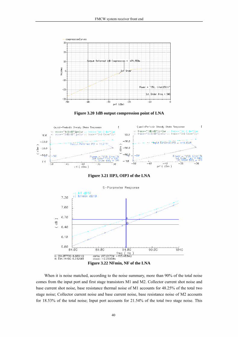
Figure 3.19 shows the S21 curve of the LNA. A 3-dB bandwidth is achieved between the bandwidth 84GHz and 104GHz. From figure 3.19, the two stage LNA also has high gain at frequency between 35GHz and 84GHz, gains outside the bandwidth will be killed later by by the band width properties of the antenna at input of the LNA and impedance matching at later stage when decoupling network and interconnects are added to the LNA. Figure 3.20 shows the 1dB compression point for the LNA when the input frequency is 94GHz. Figure 3.21, shows the OIP3, IIP3 of the LNA, the two tone frequencies are 94GHz and 94.1GHz.. From figure 3.22, at 94GHz, NFmin=6.5dB, while NF=6.66dB. Noise matching is well achieved.
Figure 3.19 S21 of the LNA
FMCW system receiver front end
40
Figure 3.20 1dB output compression point of LNA
Figure 3.21 IIP3, OIP3 of the LNA
Figure 3.22 NFmin, NF of the LNA
When it is noise matched, according to the noise summary, more than 90% of the total noise
comes from the input port and first stage transistors M1 and M2. Collector current shot noise and base current shot noise, base resistance thermal noise of M1 accounts for 48.25% of the total two stage noise; Collector current noise and base current noise, base resistance noise of M2 accounts for 18.53% of the total noise; Input port accounts for 21.54% of the total two stage noise. This

FMCW system receiver front end
41
simulation result agrees with the noise analysis in section 3.2.3 that the existence of the parasitic capacitance makes the cascode noise more significant. Also, from table 3.1, at such high frequency, collector current noise and base resistance thermal noise become most dominant noise sources.
Table 3.1 noise contribution percentage of the first stage transistor
Collector current shot noise percentage
Base resistance Thermal noise percentage
Base current shot noise percentage
M1 29.58 17.86 0.81 M2 13.72 4.51 0.30
3.4.1.2 wideband low-Q interstage matching LNA
Besides simple inter stage network in section 3.4.1.1, a wideband low Q inter stage matching LNA is also studied and compared.
Figure 3.23 the structure of LNA stage
A wide bandwidth low-Q interstage matching LNA is also studied. Figure 3.23 shows the structure of the two stage cascaded cascode low-Q interstage matching LNA. As having been mentioned in section 3.3.1, at such high frequencies 94GHz, the Sopt and S11 of are nearly conjugate at the Smith Chart, thus simultaneous impedance and noise matching can be obtained by the input matching network. Pad capacitance cannot be neglected, and it is included as part of the input impedance matching network. The pad size is 101um*101um with capacitance according to the simulation around 46fF. In order to adapt the pad capacitance, the size of the input transistor is selected as 12um/0.12um. Thus the power consumption is a little high; the first stage consumes 8mA, the second stage 16mA. In the first cascade stage, transmission line TL1 is working as an inductive load; and in the second stage, transmission lines TL2, TL3 and the dc decoupling mim capacitor comprise the output impedance matching network, which realize the power match between the LNA and the subsequent balun. The low-Q impedance matching principle of the inter-stage matching network is shown as in figure 3.24. The load represents the input impedance looking into the input transistor of the second stage cascode; the source represents the impedance looking into the output impedance of the first cascode stage. The impedance matching network is realized in the low Q region thus to realize the high bandwidth. In figure 3.24, open stub is utilized

FMCW system receiver front end
42
as shunted capacitor in the real schematic, while the series capacitor is very small, around 14fF, which is intended to be realized by plate capacitor, which is not in the library and should be designed by careful calculations.
In order to achieve the gain flatness over the specification target, the matching of the each stage is designed separately for gain shaping. In order to conquer fast roll off at higher frequencies, the output matching network is tuned at 96 GHz, and the interstage matching network is tuned at 98GHz.
Figure 3.24 low Q inter stage matching network
The performance of the low Q interstage matching LNA is shown in the figure 3.22 and 3.23. A 3dB bandwidth is achieved between 84GHz and 104GHz. Simultaneous impedance and noise matching is achieved through the bandwidth, with S11 and Gmin both smaller than -9.5dB throughout the bandwidth.

FMCW system receiver front end
43
Figure 3.25 S21 of the LNA
Figure 3.26 simultaneous impedance and noise matching
3.4.2 inductive degeneration cascode LNA[19]
Inductive degeneration is a very popular low noise technique. It utilizes a degeneration inductor to realize impedance matching without introduction of additional noise. Figure 3.27 shows the resistive termination realized by inductive degeneration.

FMCW system receiver front end
44
Figure 3.27 resistive termination by inductive degeneration
According to the gyration, we can write the input impedance like:
1( )
= ( )
in e e b
e e bm
Z L j L LC
L j L Lg
Τπ
ΤΤ
= ω + ω +ω −ω
ωω + ω +ω −
ω
(equation 3.9)
0e
T
ZL =ω
(equation 3.10)
mgT
b eL L2
ω= −ω
(equation 3.11)
Proper choice of mg , Le, and Cπ yields a 50 Ohm real part. In practice, the last two terms
may not resonate at the frequency of interest, necessitating the use of inductive component Lb at the input. Besides, the reduction of the equivalent transconductance as a result of degeneration will reduce the gain, and therefore magnify the noise contributed by the devices connected to the collector of the transistor.
For lower frequency, inductive degeneration is narrow band technique, nevertheless for such
high frequency, for a typical 6um bipolar transistor 1 5Cπ
≈ Ωω
, thus 5 0.1
50Q = = .
Figure 3.28 is the schematic for the single stage inductive degeneration LNA. The length of the transistor M1 and the inductive rfline L1 are carefully tuned to make the real part of S11 near the r=1 circle in the Smith Chart while at the same time making S11 nearly conjugate to Sopt. Note that Le doesn't affect the real part of Zsopt [25].After optimization, L1=72pH and length of transistor 6um are chosen. Then rfline L2 is tuned to achieve simultaneous impedance and noise matching at the input. Finally, L2=40pH is chosen. Figure 3.29 shows the S11 and Sopt simulation result.
Figure 3.30 shows that S22 is tuned at around 97GHz, and from S21 we can see that inductive degeneration single stage gain can only obtain 8-9dB gain. Also from figure 3.30, it is verified that inductive degeneration is wideband at such high frequency. Comparing with that

FMCW system receiver front end
45
the cascode single stage which can obtain 10 dB or even more gain, we can see that for the specific case that up to frequencies as high as 94GHz, the common emitter cascode stage can have comparable impedance and noise matching while maintain high gain. Thus inductive degeneration is inferior to cascode LNA for the 94GHz application.
Figure 3.31 shows the NFmin and NF of the single stage LNA, from which we can see that inductive degeneration could reduce the NFmin a bit but not too much. And the noise performance is comparable with that of the cascaded cascode LNA.
RFin
TL1
M1
M2
C1
VCC=2.5V
1p
CbypTL2
mim1
Inductive rfline L2
Inductive rfline L1
RFin
Figure 3.28 single stage inductive degeneration LNA
Figure 3.29 simultaneous impedance and noise matching at input port
FMCW system receiver front end
46
Figure 3.30 S22 and S21 of the single stage LNA
Figure 3.31 NFmin and NF for the single stage In order to include the pad capacitance into the matching network, the emitter length should
be scaled even longer,[25] thus with comparable noise performance, power consumption will be even larger.
3.4.3 common base input two stage LNA[13]
Common-base configuration is another popular circuit topology for bipolar LNA. This circuit offers advantages like: simple input matching, high linearity, and great reverse isolation. In a common-base circuit, the source resistance, Rs, linearizes the input output characteristic by softening the emitter current excursions. Common-base configuration also exhibits a high reverse isolation if the base bias is properly bypassed. The primary drawback of this configuration is high noise figure. Not only collector shot noise, the base resistance thermal noise, and as well the noise of the bias current all adds noise to the circuit.
For the frequencies as high as 94GHz, due to gyration of the base resistance, input impedance of the common-base configuration is inductive, such as shown in figure 3.33. Figure 3.33 shows

FMCW system receiver front end
47
the S11 and Sopt of a common-base configuration (length of the bipolar is 6um) at the bandwidth 94GHz and 104GHz. From figure 3.33 we can see that simultaneous impedance matching and noise matching are difficult to achieve. Thus noise figure will be considerably higher.
Rc
VbRs
Rin
Vout
Figure 3.32 Common-base LNA
Figure 3.33 the S11 and Sopt of common-base configuration
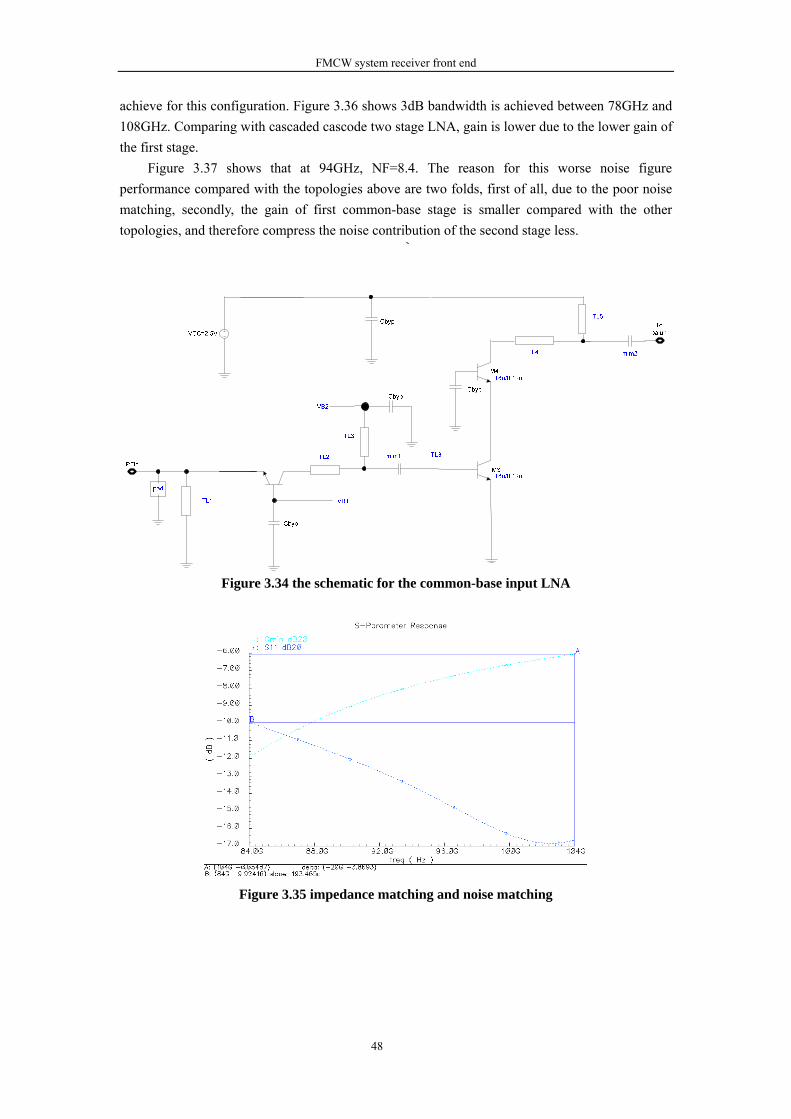
Figure 3.34 shows the schematic for the common-base input configuration. Due to the clever
use of shunt transmission line TL1, the current source is omitted, thus the noise incurred by the current source is excluded. Inter stage matching is realized by transmission line TL2, TL3. Pad capacitance is included in the input power matching.
S parameter simulation result for impedance matching and noise matching are shown in figure 3.35. From this figure , simultaneous impedance and noise matching is rather difficult to
FMCW system receiver front end
48
achieve for this configuration. Figure 3.36 shows 3dB bandwidth is achieved between 78GHz and 108GHz. Comparing with cascaded cascode two stage LNA, gain is lower due to the lower gain of the first stage.
Figure 3.37 shows that at 94GHz, NF=8.4. The reason for this worse noise figure performance compared with the topologies above are two folds, first of all, due to the poor noise matching, secondly, the gain of first common-base stage is smaller compared with the other topologies, and therefore compress the noise contribution of the second stage less.
Figure 3.34 the schematic for the common-base input LNA
Figure 3.35 impedance matching and noise matching

FMCW system receiver front end
49
Figure 3.36 S21 of LNA
Figure 3.37 NFmin and NF
3.5 comparison of different topologies of LNA
Table 3.1 give a conclusion upon the three different topologies with respect to gain, noise figure, matching, isolation, stability and so on.
From table 3.1 Inductive degeneration LNA has comparable noise performance with cascadeded cascode LNA and low Q inter stage matching LNA, but its gain performance is inferior to them.
Common base and low Q inter stage matching network LNA have the best bandwidth performance. Nevertheless, gain and noise performance of common base is inferior to low Q inter stage matching LNA and cascaded cascode LNA.
The cascaded cascode topology and low Q interstage matching LNA have the best gain, comparable noise figure with others, simultaneous matching can be easily achieved, good isolation and stability. Low Q impedance inter stage matching LNA can achieve widest bandwidth and flat gain compared with cascaded cascode configuration, but it requires small value capacitances like 14fF in the interstage matching network. And for such high frequencies, it is especially difficult to

FMCW system receiver front end
50
design accurate and small value capacitances. Also note that the power of Low Q impedance inter stage matching LNA is two times that of the cascaded cascode topology. Thus finally simpler interstage matching network without small value capacitance is preferred.
Table 3.1 Comparison of three different topologies for LNA at 94GHz
Cascaded cascode
Low Q impedance matching(2 times in power)
Inductive degeneration (single stage)
Common-base
gain High High lower Lower Noise figure good good good Worse due to
poor matching Simultaneous matching
Easy to achieve Easy to achieve can be achieved with careful design
Difficult to achieve
isolation Good (S12=-63dB @94GHz)
Good (S12=-62dB @94GHz)
Good (S12=-25dB@94GHzfor single stage)
A little worse, but still good (S12=-47dB @94GHz)
stability K>1 K>1 K>1 K>1 Small capacitor in interstage matching
no yes no no
3dB Bandwidth
84GHz-107GHz 77GHz-105GHz 87GHz-108GHz 78GHz-108GHz

FMCW system receiver front end
51
4 Specification and design of mixers
In this chapter, specifications upon design of mixers are firstly discussed, and then noise analysis of the mixer at such high frequency is given. Then the design procedure, optimization procedure of mixer are given in detail. Finally, output buffer for measurement and further signal summation are discussed.
4.1 Specifications of mixers
4.1.1 conversion gain
Conversion gain is defined as the ratio of the desired IF output to the value of the RF input.
Conversion gain is mainly determined by the mg of the transconductance stage and the value of
the load resistors.
4.1.2 noise figure
In a typical mixer, both the desired RF signal and the other image signal will generate a given
intermediate frequency. For example in figure 4.1, if 1Rf is the desired if input signal, then 2Rf
is its image. The image and desired inputs both mix with the LO and downconvert to the same frequency. The term SSB indicates that the desired signal spectrum resides on only one side of the LO frequency, DSB indicates that the desired signal spectrum resides on both sides of the LO frequency. SSB noise figure of a mixer is 3dB higher than the DSB noise figure if the signal and image bands experience equal gains at the RF port of a mixer.
Figure 4.1 image in mixers

FMCW system receiver front end
52
Figure 4.2 Frequency translation of white noise in mixers
Noise figure of mixers tend to be considerably higher than those for amplifiers since the noise from frequencies other than at the desired RF can also mix down to the IF, as shown in figure 4.2.
It is mainly because of this large mixer noise that one uses LNAs in a receiver. If the LNA has sufficient gain, then the signal will be amplified to levels well above the noise of the mixer and subsequent stages so the overall receiver NF will be dominated by the LNA noise instead of that of the mixer.
4.1.3 isolation
It is generally desired to minimize the interaction among the RF, IF, and LO ports. The LO-RF feedthrough results in LO leakage to the LNA and eventually the antenna, whereas the RF-LO feedthrough allows strong interferers in the RF path to interact with the local oscillator driving the mixer, resulting in undesired down conversion to IF of these products. The LO-IF feedthrough is important because if substantial LO signal exists at the IF output even after low-pass filtering, the IF gain stage may be desensitized. Finally the RF-IF isolation determines what fraction of the signal in the RF path directly appears in the IF, a critical issue with respect to the even-order distortion problem in homodyne receivers, but most likely less relevant in our submmwave radar application.
4.1.4 Linearity
Linearity is mainly determined by the transconductance stage non-linearity. Theoretic analysis is the same with that in LNA. Inductive degeneration can be used to improve the linearity of the transconductance stage.

FMCW system receiver front end
53
4.2 noise analysis of double balanced mixer
M1 M2
M3RF+
LO+LO-
RloadRload
Vcc
Figure 4.3 single-balanced mixer
Consider the single-balanced mixer shown in figure 4.3, we can identify three sections in the
circuit: the RF section, the time-variant section, and the IF section. For the RF section, the thermal noise due to the base resistance of M3, and the collector shot
noise of M3 constitute the principal components. For this section, the noise contributed by the base resistance and collector shot noise can be optimized by inductive degeneration as shown in figure 3.27. Inductive generation will also improve the linearity of the mixer transconductance stage.
For the time-variant section , when one of the transistors M1, M2 is on, as shown in figure 4.4, in this situation the switching pair pumping noise into the output because the parasitic capacitance at node P, Cp, which provides a finite impedance to ground. This Cp includes the
base-emitter capacitance Cπ of the M1 and M2, the collector-base junction capacitance and
collector-substrate capacitance sC of M3. Thus the RF noise due to the base resistance and
collector current of M1, M2 is translated to IF by the switching action of this transistor.

FMCW system receiver front end
54
2nI2
nV
Figure 4.4 noise contribution by the one of the collector current of the switching pair
From above observations, we can conclude that there are tradeoffs in optimizing the noise
performance. Lowering Cp, which translates to smaller sizes for M1, M2 and hence higher base resistance noise; reducing the base resistance of M1, M2, which leads to higher Cp. Thus a careful choice of device size have to be chosen. Besides, in this project, in order that the instantaneous current of the switching pair doesn't exceed the peak fT current, the transistor size of the switching pair cannot be too small.
Another effective method which should be mentioned here is decreasing the collector currents of M1 and M2. Since M1, M2 appear in the signal current path, their shot noise current,
2 2n CI qI= , directly corrupts the signal and is lowered if CI decreases. Independent values of
collector currents in M3, and M1-M2, would help improve the noise performance. Current bleeding, as shown in figure 4.5, could be introduced here to reduce the collector currents of M1, M2. Furthermore, for a given allowable voltage drop across the load resistor Rload, the value of these resistors can be increased , thus raising the voltage conversion gain. This approach, however, faces two important issues. First, as the collector current of M1 and M2 is lowered, the impedance seen looking into their emitters rises, allowing more RF current provided by M3 to be shunted to ground through Cp. Secondly, the noise current arising from Is itself directly adds to the RF signal. For these reasons, the percentage of Is to the mixer should be carefully chosen.

FMCW system receiver front end
55
M1 M2
M3RF+
LO+
RloadRload
Vcc
Is
LO-
Figure 4.5 current bleeding by Is to reduce noise
4.3 design process
4.3.1 bias of the transistors
Figure 4.6 shows the schematic for the double balanced mixer. Resistive tail current bias is introduced for the mixer. A voltage headroom of 1V is given for
the tail current bias. And the value for the Rbias is determined by the emitter current of the two RF transistors.
The bias for the RF section transistors are the same with that of LNA. The cut-off frequency vs collector current for the bipolar transistor 6u/0.12u is the same as in figure 3.7, the extrapolation frequency point is 40GHz. The peak fT frequency reaches 185GHz. Throughout the whole design, the bipolar transistor would work at the bias point which is half peak fT current, with its respective Vbe=870mV. Due to the cascode connection between the switching quad and the input differential pair, the swing is small and these transistors can be operated at the edge of saturation to save the voltage headroom[14]. (VCB=0.1V).
Vcc=3.6V is chosen as the supply voltage. In order to realize the maximum voltage swing for the output IF signal, the collector of the switching pair is chosen as the average of the supply voltage and the base of the switching pair.
A capacitor is placed in parallel with the load resistor to filter the higher mixing frequency
component LO RFω +ω . The value of the capacitor is chosen that combined with the load
resistor yielding a 3dB bandwidth higher than the output IF bandwidth 500MHz. All the voltage values of crucial nodes are illustrated in figure 4.6.

FMCW system receiver front end
56
Figure 4.6 the schematic of the double balanced mixer
4.3.2 inductive degeneration
Inductive degeneration is applied here to both optimize the noise performance of the lower stage and improve the linearity under the condition that gain drop due to the inductive degeneration at high frequencies is acceptable.
Simultaneous impedance and noise matching for the lower stage is done as shown in figure 4.7. Rbias in figure 4.6 is removed at first. Because Rbias is common mode for the input RF signal and helps improve the CMRR of the mixer, it can be removed in the analysis in noise and impedance matching for the input RF signal. Single-ended RF signal is injected through port 1.Voltage source V1 detects the noise current through the collector of M6, and current control current source CCCS feed the detected noise current to output port 2. Then procedure of impedance and noise matching of the lower stage is the same with that of the inductive degeneration LNA.
The procedure is as follows. The length of the transistor M5, M6 and the inductive rfline1 are carefully tuned to make the real part of S11 near the r=1 circle in the Smith Chart while at the same time making S11 nearly conjugate to Sopt. After optimization, L1=72pH and length of transistor 6um are chosen. Then rfline2 is tuned to achieve simultaneous impedance and noise matching at the input. Capacitor Mim is used to realize the ac coupling. The value of mim is carefully chosen, it should not be too small to affect the noise and impedance matching, while it should not be too large for the parasitic capacitance to ground would be too large. Besides, the position of mim capacitor is preferred secondary after the rfline2 rather than next to the RF input transistor, because the input impedance of the transistors is very small compared to the 50 Ohm output impedance of the retrace hybrid. Thus the interference of the mim capacitor to the impedance matchig will be much less.

FMCW system receiver front end
57
Figure 4.7 simultaneous noise and impedance matching
The simulation result for the simultaneous impedance and noise matching at the differential RF input for the RF section is shown as in figure 4.8.
Figure 4.8 simultaneous impedance matching and noise matching at the differential RF input
4.3.3 current bleeding
As illustrated in section 4.2.1, current bleeding can be applied to reduce the noise contribution of switching pair while improve the conversion gain at the same time. However, tradeoff exists between the current percentage. If the percentage is too low, then the noise and gain improvement will be small; if the percentage is too high, then the parasitic capacitance Cp will become relatively more significant, and conversion gain will begin to saturate. Thus various current bleeding percentages are tried to achieve a conclusion.
Figure 4.9 shows the conversion gain vs the resistor current bleeding percentage of the input

FMCW system receiver front end
58
RF transistor. Figure 4.10 shows the noise figure vs current bleeding percentage. For each current percentage, supply voltage remains the same, while load resistors are adjusted. The size of switching transistors are always smaller than the input RF transistors, in order to have high switching speed. Nevertheless, the switching transistors cannot be too small, because the current through it should be within half the peak fT current of the transistor for safety reasons. Thus the length of the switching pair is chosen as 5um.
From both figures, the conversion gain and noise figure improves with the bleeding current percentage but begin to saturate around 80% and 90% , and in this project, 70% percent is selected as the current bleeding percentage for safety. All of these voltage gain comparisons are done under the same bias and transistors, rflines, except for the load resistor value and bleeding resistor value.
Conversion gain
8.569.56
1112.0211.93
8.74
02468
101214
40% 60% 80% 100%
percentage of current bleeding
voltage conversion
gain
Conversion gain
Figure 4.9 voltage gain vs current bleeding percentage
NF
12.5
13
13.5
14
40% 60% 80% 100%
current bleeding percentage
NF
NF
Figure 4.10 NF vs current bleeding percentage
4.3.4 The mixer performance
The variation of power gain with the RF input frequency is shown as in figure 4.11. Power gain decreases with the increasing of the frf, this is both because of the inductive degeneration and the high frequency roll off.

FMCW system receiver front end
59
Power gain
11.5
12
12.5
13
13.5
14
80 90 100 110
frf
power gain
Power gain
Figure 4.11 power gain vs frf
Figure 4.18 shows the SSB noise figure of the mixer variation with the RF input frequency.
NF
11
12
13
14
80 90 100 110
frf
noise figure
NF
Figure 4.12 noise figure vs frf
Table 4.1 gives an overall performance of the mixer at 94GHz input frequency.
Table 4.1 Overall performance of the mixer at 94GHz input frequency
Power gain
Noise figure
1dB compression point
OIP3 LO-IF isolation
LO-RF isolation
RF-LO isolation
RF-IF Isolation
12.7dB 12.7dB -0.59dBm 11.07dBm -54dB <-100dB <-160 <-150
Figure 4.13 is the noise figure for the dc-couppled-output-buffer mixer. The 1/f corner frequency is around 1KHz.

FMCW system receiver front end
60
Figure 4.13 noise figure of the dc-coupled-output-buffer mixer
4.3.5 The mixer performance comparison before and after
noise optimization
Table 4.2 shows the performance comparison of the mixer before and after noise optimization for the RF input frequency 94GHz, and the local oscillating frequency 94.5GHz, with the same supply voltage 3.6V, the same size of transconductance transistors. From the comparison, the power conversion gain , linearity, noise figure improve a lot after the optimization.
Nevertheless, after optimization, noise contribution of the switching core becomes even larger than that of the transconductance stage, this is due to the gain reduction when inductive degeneration is utilized to improve linearity and optimize noise. Thus linearity and noise trade off exists when inductive degeneration is applied. More consideration should be given upon this for future work. If without considering improvement upon linearity, the same simultaneous noise and impedance matching applied in LNA combined with current bleeding will be a good choice to optimize noise performance and boost the gain.
Table 4.2 comparison before and after noise optimization
Power Conversion gain
Noise figure
Output referred 1dB compression point
OIP3
Before optimization
4.84dB 14.37dB -3.94dBm 8.1dBm
After optimization
12.67dB 12.7dB -0.59dBm 11.07dBm
4.3.6 buffers and open collector current adder
Figure 4.14, figure 4.15 shows the two solutions for the output buffer of the mixer in simulation including the dc coupled output buffer and ac coupled output buffer. In simulation, dc coupled circuit is necessary for the correct simulation of noise figure of the mixer. Because large capacitor in ac coupled buffer will distort the 1/f noise simulation result.
For measurement, in real circuit implementation, differential common emitter buffer stages

FMCW system receiver front end
61
will follow the figure 4.14, with the ac coupling capacitor removed from figure 4.14, so that DC coupled output buffer is realized, as shown in figure 4.16. The load of differential common emitter gain stages will be 50 Ohm to reduce reflection.
Because when many of these receivers are used to deliver the down converted signals of the receivers , analogue signal summation is needed at the output of these chips, figure 4.17 shows the open collector output for the mixer, then multiple current signals could be added conveniently.
Figure 4.14 AC coupled output buffer
Figure 4.15 DC coupled output buffer

FMCW system receiver front end
62
Figure 4.16 further buffer stages for measurement
Figure 4.17 Open collector current adder

FMCW system receiver front end
63
5 overall performance and verification
In this chapter overall performance of the LNA mixer chain is given and system verification upon the image problem in the chain is carried out.
5.1 overall performance
A passive ratrace hybrid is inserted between the two stage single ended LNA and the double balanced mixer, acting as a balun.
The schematic for the testing of the ratrace hybrid is shown as in figure 5.1. The SP simulation result for the ratrace hybrid is shown as in figure 5.2 and figure 5.3. Wide bandwidth is provided between 80GHz and 110GHz, and thus can be utilized as balun to connect the LNA and mixer. Note that for the balun, there is around 0.6dB-0.8dB amplitude loss in each signal path.
Figure 5.1 schematic for the simulation of the balun

FMCW system receiver front end
64
Figure 5.2 reflection coefficients at each port of the balun
Figure 5.3 S21 and S31 of the balun
The overall power gain and noise figure for the LNA-mixer chain is shown as in figure 5.4 and 5.5. 4dB bandwidth is achieved from 84GHz to 104GHz. For the overall voltage gain, there will be 3dB increase due to the single-ended 50 Ohm at the input of LNA to differential mixer output impedance 100 Ohm. The overall noise figure is increased from 9.2 to 10.2 within the bandwidth. Taking the 96GHz frequency point as an example, the gain of LNA at that frequency is around 23.3dB, the power gain of the mixer is around 12.6dB, the overall power gain is 34.8dB, thus insertion of the balun, adds about 0.7dB loss to the circuit. This agrees with the SP simulation result in figure 5.3 that introduction of the balun would introduce 0.6-0.8dB power gain loss. At higher frequencies, the overall power gain drops rapidly. The gain roll-off also results from the inductive degeneration in the mixer.
Due to the existence of image of the LNA, the Friss equation should be modified as
2,1,
12*(1 1) DSB
tot DSBP
NFNF NF
G−
= + − + (equation 5.1)
Considering the 94GHz frequency point as an example, the NFtot should be
2,1,
12.7 36.67 1010
23.310
12*(1 1)
10 1 2* 1 10 110
9.7
DSBtot DSB
P
NFNF NF
G
dB
−
−= + − +
⎛ ⎞ −= + − +⎜ ⎟
⎝ ⎠
=
(equation 5.2)
And by simulation the overall NF rises to 9.9dB. Table 5.1 shows the gain, noise, linearity, power performance throughout the whole chain.

FMCW system receiver front end
65
overall power gain
30
31
32
33
34
35
80 90 100 110
frf
overall power gain
overall power gain
Figure 5.4 overall power gain
NF
9.2
9.4
9.6
9.8
10
10.2
80 85 90 95 100 105 110
frf
Overal noise figure
NF
Figure 5.5 overall noise figure
1dB@output
-1
-0.8
-0.6
-0.4
-0.2
0
0.2
0.4
0.6
80 85 90 95 100 105 110 1dB@output
Figure 5.6 1dB@output vs frf

FMCW system receiver front end
66
-33
-32.5
-32
-31.5
-31
-30.5
-30
-29.5
-29
-28.5
80 85 90 95 100 105 110
frf
1dB@input
系列1
Figure 5.7 1dB@input vs frf
Table 5.1 gain, noise, linearity, power performance throughout whole chain
NF@94G S21@94G Output
referred 1dB Compression
Power Current
LNA1 6.4dB 11.5dB -0.45dBm 4.4*2.5=11mW 4.4mA
LNA2 7.57dB 10dB -0.21Bm 8.4*2.5=21mW 8.4mA
LNA1_2 6.66dB 23.3dB -0.47dBm 12.8*2.5=32mW 12.8mA
Mixer 12.7dB CG=12.7dB-0.59dBm 7.4*3.6=26.6mW 7.4mA
Overall 9.9dB CG=34.5dB-0.79dBm 26.6+32=58.6mW
Output buffer
20*3.6=72mW 10*2mA
Bias circuits
1.2*2*2.5+ 1.2*3.6=10.32mW
Overall (including bias and buffer)
32+26.6+58.6 +72+10.32=141mW

FMCW system receiver front end
67
Figure 5.8 noise figure
Figure 5.6 shows the output referred 1dB compression point vs input frequency, the output
referred 1dB compression point is roughly around 0dBm throughout the bandwidth. Figure 5.7 shows the input referred 1dB compression point vs input frequency.
Figure 5.8 shows the noise figure vs IF frequency. From figure 5.8, the corner frequency is around 10Hz.
5.2 system verification upon noise figure
Figure 5.9 system verification by ADS
In order to provide more insight in the 3dB noise degradation due to the introduction of the
mixer, a system verification is performed in ADS. As shown in figure 5.9, an ideal LNA with noise figure 6.5dB and gain 20dB is defined, with input and output ideally matched. An ideal noiseless mixer with 12dB conversion gain is defined. Figure 5.10 shows the simulation result for 5.9. The overall noise figure increase by 3dB. The increase is because of the existence of image noise. For linear sweeping frequency from 84GHz to 104GHz, it is impossible to reject the image frequency

FMCW system receiver front end
68
in direct conversion architecture unless, as discussed in chapter 1, image-reject architecture is utilized, which is quite complicate to realize at 94 GHz. To further confirm this explanation, a second system verification is carried out.
Figure 5.10 overall noise figure
As shown in figure 5.11, all other parts in figure 5.9 remain the same , while an ideal
bandpass filter is inserted in the chain, which allows the signal while reject image frequency, and a new simulation result is given in figure 5.12. Now the noise figure doesn't degrade by 3dB, and the explanation that noise in the image brings 3dB in noise figure is confirmed. Note that it will not be possible in practice to perform such a filtering, therefore if one wants to avoid the noise degradation, single sideband down conversion schemes should be utilized as discussed earlier in this thesis.
Figure 5.11 an image filter is inserted into the system
Figure 5.12 the new overall noise figure

FMCW system receiver front end
69
6 More upon LNA
In this chapter, bias circuits for the LNA is discussed, and stability checked; decoupling network is added to the LNA; after including all interconnects and decoupling network, performance of the LNA is given. Finally, process and temperature variation of LNA are given.
6.1 bias circuits for the LNA
Figure 6.1 bias circuits for the LNA
The bias circuits for the LNA are shown in figure 6.1. BASE1 sets the base bias voltage for
the common emitter transistor, CAS1 sets the base bias voltage for the cascode transistor. Resistors R1 and R2 not only forces the base-emitter voltage of M1 and M2 equals to the common-emitter transistor of the LNA, but as well are chosen large values to reduce noise contribution by the bias circuits. With resistor R3 and R4, voltage CAS could be easily tuned. Current sink could be added for the M2 to tune the current supply of the LNA in order that under different process corners, temperature conditions, the LNA still can perform normally.
All the current density limits of resistors in the bias circuits are checked. Because the bias circuit forms positive current feedback by the two current mirrors M1&M2,
M4&M3, there is potential stability problem. The stability of the bias circuit is checked by ac simulation. First open the loop at the emitter of M4. All the bias voltages of transistors remain the same. An AC current is connected at the emitter of M4, ac current response is obtained at the other open point. The schematic is shown in figure 6.2. The ac simulation result is shown as in figure 6.3.. From figure 6.3, the current gain remains below 1 throughout all the frequencies from 1Hz to

FMCW system receiver front end
70
100GHz. In order to further verify the stability, the rise time of the step is 1ns, figure 6.4. (50nsec
verified, 20MHz; up to 1us, 1MHz)
CAS
BASE
VCC
R1 R2
R4
R3
M1M2
M3M4
V1
Ic
Figure 6.2 ac simulation schematic for the bias circuit
Figure 6.3 ac simulation result for the bias circuit

FMCW system receiver front end
71
Figure 6.4 time step response
6.2 decoupling
Figure 6.5 off chip supply decoupling network
Figure 6.5 shows the offchip decoupling network for the supply of LNA.. L1, L2 represents the estimated inductance of the PCB. L4 and L3 represents the parasitic inductance of capacitors C1 and C2. R1 and R2 are de-Q resistors to increase the bandwidth of resonance. L5 is DC feed.
C1 and L4 resonates at the frequency 1 500
2 4* 1MHz
L C≈
π; C2 and L3 resonates at the
frequency 1 160
2 3* 2MHz
L C≈
π. Even more capacitors like C1 and C2 can be added into
the decoupling network . This supply decoupling network is realized off chip.

FMCW system receiver front end
72
Figure 6.6 ac ground @ f0
Figure 6.6 shows the ac ground at frequency 0 94f GHz= .At such high frequency, even a
short length of interconnect cannot be neglected, and is included in the resonance ac ground.
Capacitors C1 and C2 are tuned to resonance with the transmission line at 0 94f GHz= . This
ac@ 0f circuit is used at both the supply decoupling and the at the base terminal of cascode, and
is realized on chip.
300fF 300fF 300fF 300fF
Figure 6.7 ac ground @ lower frequency
Figure 6.7 shows the ac ground@ lower frequency. 4*300fF capacitors are in parallel to realize the ac ground for lower frequencies. At 50 GHz, the impedance of the ac ground is
about1 3.4j
j C= −
ωOhm. This decoupling network is connected at the supply decoupling
network , and is realized on chip.
C=40fF
Gounded stub

FMCW system receiver front end
73
Figure 6.8 simple high pass filter at the input of LNA
Because 0f is so high, complete decoupling for lower frequencies is very difficult to
achieve, and after decoupling network, there are peaks at the lower frequencies in the S21 curve, in order to attenuate these peaks, and as well suppress the high gain at lower frequency range (50GHz to 70GHz ) , a simple high pass filter is added at the input of the LNA. The small capacitor with value of 40fF can be realized by plate capacitor. The size of the capacitor can be
determined by hand calculation according to the definition of capactor: 4
SCd
= επ
. ε is the
permittivity of the dielectric, S is the area of the dielectric, d is the distance between the two plates.
Plate capacitor is utilized because at the input, use of mim capacitor demands ESD protection, while ESD would introduce much parasitic capacitance at such high frequency, and degrades the RF performances seriously. Thus plate capacitor is preferred. Although the estimated value of plate capacitor may be not accurate, uncertainties at the input are many, like the modeling of the bondpad, the flip chip package and so on.
RFin
TL1
M1
M2
M3
M4
6u/0.12u
6u/0.12u
12u/0.12u
12u/0.12u
To balun
pad
TL4
TL3mim1TL5C=40fF
VCC=2.5V
VCC=2.5V
ac@f0
ac@f0
Offchip supply decoupling
ac@lower frequency
ac@f0
ac@f0
Offchip supply decoupling
ac@lower frequency
Figure 6.9 LNA including high pass filter, off chip supply decoupling,
and ac ground for f0 and lower frequencies

FMCW system receiver front end
74
Figure 6.10 bypass capacitor ac@lower frequency added at the bias circuit
Figure 6.9 shows the schematic of LNA including off chip supply decoupling, ac ground@f0, ac ground at lower frequencies, and the high pass filter at the input. Y junctions are utilized in the high pass filter and decoupling networks. Tapers are inserted between transmission lines and transistors, Y junctions and mim capacitors, mim capacitors and transmission lines and so on.
Figure 6.10 shows that bypass capacitor ac@lower frequency is added at the bias circuit. Figure 6.11 shows the 3dB bandwidth of S11 through 77GHz and 112GHz, after adding all
above mentioned decoupling and interconnection. In figure 6.12 S11 and Gmin are all below -10 throughout the 3dB bandwidth, while S22 degrades a bit. In figure 6.13, NF is close to NFmin, and noise matching is well achieved.

FMCW system receiver front end
75
Figure 6.11 3dB bandwidth throughout 77GHz-112GHz
Figure 6.12 S11, Gmin and S22 of the LNA

FMCW system receiver front end
76
Figure 6.13 NFmin and NF of the LNA
Stability factor K>1 is checked throughout the whole frequency range from 1MHz to
120GHz.Nevertheless, due to the decoupling near DC frequency is not perfect, at very low frequency, K>1 is not satisfied. Time domain simulation is also checked, at very low frequency there are resonance signal, nevertheless, the amplitude of the resonance signal is very small.
6.3 process and temperature variation
Figure 6.14 temperature variation of LNA

FMCW system receiver front end
77
Figure 6.14 shows 3dB S21 variation of the LNA when temperature changes from 25o C to
100o C .
Figure 6.15 process variation of the LNA
Figure 6.15 shows 3± dB S21 variation of the LNA when process changes from -1 to 0, to
+1.
CAS
BASE
VCC
R1 R2
R4
R3
M1M2
M3M4
Currentsink
R1
R2
Figure 6.16 Current sink

FMCW system receiver front end
78
Figure 6.16 shows that, in order to compensate the process variation, a current sink could be added to the bias circuit. When in high process corner, current should be sunk from the bias, while in low process corner, it shouldn't.
6.4 Layout for LNA and mixer
Figure 6.17 the layout of LNA

FMCW system receiver front end
79
Figure 6.18 layout for mixer
Figure 6.17, 6.18 shows the initial layout for LNA and mixer. Interconnects like Y junction,
tapers which are available models in the library, and also there are interconnects like metal strips which are not available in the library, and should be further verified by ADS momentum.
For LNA, the most critical metal strip is the emitter to ground connection at the common emitter transistor. This interconnect will behave like an inductor at such high frequency and degrade the performance of the LNA . Thus in the layout it is carefully designed. In the layout, the emitter is connected to ground by two parallel interconnects and the interconnects are designed as short as possible (two 2um*5um metal strip). For a typical Deep Trench rfline with width 4um,and length 100um, its inductance is 70pH. Comparing this with the metal strip, conservatively, if the metal strip is estimated as 10pH, a simulation is given by sweeping the inductive degeneration of the LNA from 1pH to 16 pH, from which the influence of the parasitic inductance at the emitter can be roughly estimated.
Figure 19 and figure 20 shows the variation of S21, S11 , Gmin of the LNA with emitter

FMCW system receiver front end
80
parasitic inductance value. From figure 19, S21 become smaller with the increasing of inductance value, nevertheless 3dB bandwidth still remains. S11 and Gmin changes little with inductance value and still remains below -10 throughout the bandwidth. 16pH parasitic inductance will introduce less than 2 dB degradation in S21, which is still tolerable.
Figure 6.19 S21 variation with the emitter parasitic inductance value
Figure 6.20 S11, Gmin variation with the emitter parasitic inductance value

FMCW system receiver front end
81
7. Conclusions
7.1 conclusions
In conclusion, a RF receiver frontend with more than 30dB power gain, less than 10dB noise figure, high LO-RF isolation and considerable linearity is realized.
For a wideband (84GHz-104GHz) single-ended input RF signal, a high performance LNA is designed and a passive balun is included to convert the single-ended RF signal to differential signal in order to drive the double balanced mixer.
Various topologies upon 94GHz LNA are studied, like cascaded cascode LNA, inductive degeneration cascode LNA, common-base LNA, and compared for their performance. The most suitable candidate with highest gain, noise performance, isolation, and so on is selected for implementation, namely the two stage cascaded cascode LNA.
A passive wideband ratrace hybrid is designed to perform the function of balun. The double-balanced mixer utilizes the inductive degeneration to optimize both linearity and
noise of the lower RF stage noise performance; while resistive bleeding technique are applied to decrease the noise contribution of the switching pair and boost the conversion gain. The bleeding percentage for the current is carefully chosen to achieve the best conversion gain and noise performance of the mixer.
7.2 further discussion
7.2.1 single-side band mixer implementation[20]
As mentioned in section 1.2.1.2, there are noise penalties for the image frequency in the proposed direct-conversion architecture, image-reject receivers are therefore considered to be good candidates to improve at this point in the future. Nevertheless, for now, due to the complexity of the image reject receivers, like generation of quadrature local oscillating oscillator signals, good matches of gains and phase shifts between the upper and lower paths at W-band frequencies, the simple direct conversion architecture is preferred. In spite of this decision at a later stage single-sideband mixers may play a key role in FMCW radar systems since they can provide a 3dB noise improvement, for this reason it is interesting to look a bit closer to their properties.
Conventional single side-band mixer topologies based on double-balanced mixers use filters
to block the image from entering the mixer, so that no down-converted image is allowed to be generated by the mixer. Since the desired and image signals are always separated in frequency by twice the IF frequency, the IF frequency must be high enough to allow the pre-selection in front of

FMCW system receiver front end
82
the mixer to block the image, but still allow the desired if signal to enter the mixer. As the IF frequency is reduced, the desired and image signals move closer together in frequency (converging on fL), forcing the selectivity of the preselector to increase in order to separate the two adjacent input signals. Preselector complexity also increases for tunable receivers because the preselector must track with the LO frequency, to maintain the normally constant IF output frequency.
In comparison to conventional DB mixers, IRMs achieve image-rejection through phase cancellation, not filtering, so the frequency spacing between the image and desired inputs can be negligible. This means that single sideband downconversion can be accomplished without pre-selection, and in fewer stages, saving the cost of extra mixers, amplifiers, local oscillators, and fitters.
In this thesis, the following single-side band mixer topology has been studied.
Figure 7.1 Block diagram of a single-sideband mixer
Figure 7.1 shows a block diagram of a single side band mixer.
Assume the input RF signal of mixer M1 is ,1( )inV t ,
,1 RF RF( ) cos sinin RF RFV t u t v t= ω + ω (equation 7.1)
After 90 degree phase shift, the input RF signal of mixer M2 is
,2 RF RF
RF RF
( ) cos( 90) sin( 90) =- sin cos
in RF RF
RF RF
V t u t v tu t v t
= ω + + ω +
ω + ω (equation 7.2)
Then mixed IF signal at output of M1 is
( ) ( )
( ) ( )
1
RF LO RF LO
LO RF LO RF
( )* ( )1 1 cos sin2 21 1 = cos sin2 2
in LO
RF LO RF LO
RF LO RF LO
V V t V t
u v t v v t
u v t v v t
=
= ω −ω + ω −ω
ω −ω − ω −ω
(equation 7.3)
Then mixed IF signal at output of M2 is

FMCW system receiver front end
83
( ) ( )
( ) ( )
2 ,1
RF LO RF LO
LO RF LO RF
( )* ( )1 1 sin cos2 2
1 1 = sin cos2 2
in LO
RF LO RF LO
RF LO RF LO
V V t V t
u v t v v t
u v t v v t
=
= − ω −ω + ω −ω
ω −ω + ω −ω
(equation 7.4)
2V after 90 degree phase shift becomes
( ) ( )'2 LO RF LO RF
1 1V = cos sin2 2RF LO RF LOu v t v v tω −ω − ω −ω (equation 7.5)
Comparing 1V with '2V , the RF signal at the output of mixer M1 and M2 are the same.
For the image siganl:
,1 IM IM( ) cos sinIM IM IMV t u t v t= ω + ω (equation 7.6)
After 90 degree phase shift,
,2 IM IM( ) sin cosIM IM IMV t u t v t= − ω + ω (equation 7.7)
The output of mixer M1 is
,1 ,1
IM LO IM LO
( )* ( )1 1 cos( ) sin( )2 2
IM IM LO
IM LO IM LO
V V t V t
u v t v v t
=
= ω −ω + ω −ω (equation 7.8)
The output of mixer M2 is
,2 ,2
IM LO IM LO
( )* ( )1 1 sin( ) cos( )2 2
IM IM LO
IM LO IM LO
V V t V t
u v t v v t
=
= − ω −ω + ω −ω(equation 7.9)
After 90 degree phase shift, ,2IMV becomes
',2 IM LO IM LO
1 1cos( ) sin( )2 2IM IM LO IM LOV u v t v v t= − ω −ω − ω −ω (equation 7.10)
Comparing ,1IMV with ',2IMV , the image signal at the output of mixer M1 and M2 are out of
phase and can be cancelled. Figure 7.2 shows the systematic simulation of the LNA-single side band mixer chain. Ideal
90-degree hybrid coupler is inserted between the 20dB gain, 6.5dB NF single ended LNA and noise less double balanced mixer. After mixer, two Ideal 90-degree hybrid coupler are inserted to provide the lower path 90 degree more phase shift, while maintaining the gain balance between the upper and lower paths. Finally, an ideal 180-degree hybrid coupler is utilized to combine the upper and lower paths.

FMCW system receiver front end
84
Figure 7.2 systematic simulation of single side band mixer in the LNA mixer chain
The overall NF of the chain is 6.51dB. If the isolation port is set to be noiseless, then the overall noise figure becomes 6.501dB. Thus the noise of isolation port cannot be cancelled. Note that implementation of the hybrids in a physical sense will be problematic. Therefore also digital options should be considered for this implementation.

FMCW system receiver front end
85
Reference [1] workplan_integrated_radars,TU delft. [2]D. C. W. Low, K. W. Chang, R. Lin, E. W. Lin, H. Wang, M. Biedenbender,G. S. Dow, and B. R. Allen, “A single-chip W-band transceiver with front-end switching receiver for FMCW radar applications,” in IEEE Microwave Millimeter-Wave Monolithic Circuits Symp. Dig.,June 1995 [3] K. W. Chang, H. Wang, G. Shreve, J. G. Harrison, M. Core, A. Paxton, M. Yu, C. H. Chen, and G. S. Dow, “Forward-looking automotive radar using a W-band single-chip transceiver,” IEEE Trans. Microwave Theory Tech., vol. 43, pp. 1659–1668, July 1995. [4] M. Vossiek, T. v. Kerssenbrock, and P. Heide, “Novel nonlinear FMCW radar for precise distance and velocity measurements,” in IEEE MTT-S Int. Microwave Symp. Dig., June 1998, pp. 511–514. [5]Lawner, R.T.; Blanchard, P.F.; Gogineni, S.P.; “Coherent FM-CW millimeter-wave radar systems for radar cross section measurements,” Instrumentation and Measurement, IEEE Transactions on Volume 39, Issue 1, Feb 1990 [6]Behazad Razavi, RF microelectronics [7]David M.Pozar, “microwave engineering” [8] Leo de Vreede, Microwave Circuit Design, ET4259, Lecture Notes, 2006,TUDelft [9] P. R. Gray, R.G. Meyer et al, “Analysis and Design of Analog Integrated Circuits”, 4th Edition, NewYork: Wiley, 2001 [10] Yaoming Sun, Frank Herzel, Johannes Borngraber, Rolf Kraemer IHP, Im Technologiepark 25, D- 15236, Frankfurt (Oder), Germany, “60 GHz Receiver Building Blocks in SiGe BiCMOS”, Silicon Monolithic Integrated Circuits in RF Systems, 2007 Topical Meeting on 10-12 Jan. 2007 Page(s):219 - 222 [11] Van-Hoang Do1, Viswanathan Subramanian2, Georg Boeck2, “60 GHz SiGe LNA”, Electronics, Circuits and Systems, 2007. ICECS 2007. 14th IEEE International Conference on 11-14 Dec. 2007 Page(s):1209 - 1212 [12] Y. Sun, J. Borngräber, F. Herzel, W. Winkler, “A fully integrated 60 GHz LNA in SiGe:C BiCMOS technology,” IEEE BCTM, pp. 14-17,Oct. 2004. [13] B. Floyd, et al., “A Silicon 60 GHz Receiver and Transmitter Chipset for Broadband Communications,” IEEE ISSCC, pp. 220-221, Feb.2006. [14] John R. Long, RF Integrated Circuit Design, ET4254, Lecture Notes,2006, TUDelft [15]Behzad Razavi, “Design of analog CMOS integrated circuits” [16]chapter 2-1,”data aquisition” [17] NI PXI/PXIe/PCI-5122 Specifications 14-Bit 100 MS/s Digitizer [18] Department BEVV,Mixed Signal Technology Development,IBM Microelectronics Division, “BiCMOS8HP Design Manual” [19] Van-Hoang Do1, Viswanathan Subramanian2, Georg Boeck2, “60 GHz SiGe LNA” Electronics, Circuits and Systems, 2007. ICECS 2007. 14th IEEE International Conference on 11-14 Dec. 2007 Page(s):1209 - 1212 [20] Bert C. Henderson, James A. Cook, “Image-Reject and Single-Sideband Mixers”, Watkins-Johnson Company, Tech-Notes [21] Thomas H. Lee, “The Design of CMOS Radio-Frequency Integrated Circuits”, Cambridge University Press 1998, Chapter 2

FMCW system receiver front end
86
[22]Scott K.Reynolds, Brian A.Floyd, Ullrich R.Pfeiffer Troy Beukea, JanusZ Grzyb, Chuck Haymes, Brian Gaucher, Mehmet Soyuer, “A silicon 60-GHz receiver and transmitter chipset for broadband communications”, IEEE Journal of solid-state circuits, vol 41, No 12, December 2006 [23] Yaoming Sun, Srdjan Glisic, Frank Herzel, “A Fully Differential 60 GHz Receiver Front-End with Integrated PLL in SiGe:C BiCMOS”, Proceedings of the 1st European Microwave Integrated Circuits Conference [24] Wolfgang Winkler, Johannes Bomgraber, Hans Gustat, Falk Komdorfer, “60 GHz Transceiver Circuits in SiGe:C BiCMOS Technology”, Solid-State Circuits Conference, 2004. ESSCIRC 2004. Proceeding of the 30th European 21-23 Sept. 2004 Page(s):83 - 86 [25] Nicolson, S.T.; Voinigescu, S.P.; “Methodology for Simultaneous Noise and Impedance Matching in W-Band LNAs”, Compound Semiconductor Integrated Circuit Symposium, 2006 IEEE Nov. 2006 Page(s):279 – 282 [26] Rohit Parthasarathy, “Fine Resolution Radar for Near-Surface Layer Mapping” [27] Paul Gray, “Analysis and design of analog integrated circuits”, fourth edition