Evolution of structural and optical properties of rutile TiO 2 thin films synthesized at room temperature by chemical bath deposition method A.H. Mayabadi a , V.S. Waman a , M.M. Kamble a , S.S. Ghosh a , B.B. Gabhale a , S.R. Rondiya a , A.V. Rokade a , S.S. Khadtare a , V.G. Sathe b , H.M. Pathan c , S.W. Gosavi c , S.R. Jadkar c,n a School of Energy Studies, University of Pune, Pune 411 007, India b UGC-DAE-CSR, University Campus, Khandawa Road, Indore 452 017, India c Department of Physics, University of Pune, Pune 411 007, India article info Article history: Received 18 April 2013 Received in revised form 16 August 2013 Accepted 5 September 2013 Available online 16 September 2013 Keywords: A. Thin films B. Chemical synthesis C. Raman spectroscopy C. X-Ray diffraction D. Optical properties abstract Nanocrystalline thin films of TiO 2 were prepared on glass substrates from an aqueous solution of TiCl 3 and NH 4 OH at room temperature using the simple and cost-effective chemical bath deposition (CBD) method. The influence of deposition time on structural, morphological and optical properties was systematically investigated. TiO 2 transition from a mixed anatase–rutile phase to a pure rutile phase was revealed by low-angle XRD and Raman spectroscopy. Rutile phase formation was confirmed by FTIR spectroscopy. Scanning electron micrographs revealed that the multigrain structure of as-deposited TiO 2 thin films was completely converted into semi-spherical nanoparticles. Optical studies showed that rutile thin films had a high absorption coefficient and a direct bandgap. The optical bandgap decreased slightly (3.29–3.07 eV) with increasing deposition time. The ease of deposition of rutile thin films at low temperature is useful for the fabrication of extremely thin absorber (ETA) solar cells, dye-sensitized solar cells, and gas sensors. & 2013 Elsevier Ltd. All rights reserved. 1. Introduction Titanium oxide (TiO 2 ) is one of the most important functional semiconductor materials. It occurs in three different crystalline phases: rutile (tetragonal), anatase (tetragonal) and brookite (orthorhombic) [1–3]. Rutile is thermodynamically stable, while anatase and brookite are metastable. Among metal oxide nanos- tructures, TiO 2 offers a range of physical and chemical properties that make it suitable for a wide spectrum of applications. Its semiconductor properties also make it a suitable electrode mate- rial for the conversion of light energy into electrical energy. Compared to other materials such as ZnO, CdS, and ZrTiO 4 that show similar properties, TiO 2 has better chemical stability and thin film transparency and is less expensive to produce [4–6]. It has been extensively explored for applications such as supercapa- citors [7], dye-sensitized solar cells [8,9], quantum-dot-sensitized solar cells [10], lithium ion batteries [11], photoelectrolysis [12], water splitting [13], biosensors [14], photochromic devices [15], self-cleaning [16], and extremely thin absorber (ETA) solar cells [17]. These applications depend strongly on the TiO 2 crystalline structure, morphology, and particle size [6,18]. Several different techniques have been used to prepare TiO 2 -based nanostructures, such as template-assisted methods [19], electrochemical anodic oxidation [20], spray pyrolysis [21], che- mical vapor deposition [22], hydrothermal methods [23], sol–gel methods [24], electrodeposition [25], oxidation of pure Ti sheets [24], eggshell membrane templates [26], electrospinning [27], chemical treatment of fine TiO 2 particles [28], and chemical bath deposition (CBD) [9,29–33]. Experimental results have shown that the preparation technique and processing conditions have a strong influence on the microstructure and physical properties of the material. Each of these methods has its own advantages and limitations. For instance, the templating technique requires a high calcination temperature to remove the template, resulting in collapse of the tubular structure of the product [34]. This high calcination temperature inevitably limits further applications in device fabrication. Anodizing processes produce nanotubes of relatively large diameter [35]. The multistep hydrothermal process requires a large quantity of inorganic solvent, which is environ- mentally unfriendly. Therefore, investigations of alternative tech- niques for deposition of device-quality TiO 2 at low temperature with the minimum use of inorganic solvents are desirable. The CBD method has attracted considerable attention in recent years as an alternative technique for the synthesis of metal chalcogenide thin films owing to its advantages of low cost and large-area deposition. In this method, thin films of metal chalcogenides are formed by spontaneous reaction in solution. Contents lists available at ScienceDirect journal homepage: www.elsevier.com/locate/jpcs Journal of Physics and Chemistry of Solids 0022-3697/$ - see front matter & 2013 Elsevier Ltd. All rights reserved. http://dx.doi.org/10.1016/j.jpcs.2013.09.008 n Corresponding author. Tel: þ 91 20 2569 2678; fax: þ 91 20 2569 1684. E-mail address: [email protected] (S.R. Jadkar). Journal of Physics and Chemistry of Solids 75 (2014) 182–187

Welcome message from author
This document is posted to help you gain knowledge. Please leave a comment to let me know what you think about it! Share it to your friends and learn new things together.
Transcript
Evolution of structural and optical properties of rutile TiO2 thin filmssynthesized at room temperature by chemical bath deposition method
A.H. Mayabadi a, V.S. Waman a, M.M. Kamble a, S.S. Ghosh a, B.B. Gabhale a, S.R. Rondiya a,A.V. Rokade a, S.S. Khadtare a, V.G. Sathe b, H.M. Pathan c, S.W. Gosavi c, S.R. Jadkar c,n
a School of Energy Studies, University of Pune, Pune 411 007, Indiab UGC-DAE-CSR, University Campus, Khandawa Road, Indore 452 017, Indiac Department of Physics, University of Pune, Pune 411 007, India
a r t i c l e i n f o
Article history:Received 18 April 2013Received in revised form16 August 2013Accepted 5 September 2013Available online 16 September 2013
Keywords:A. Thin filmsB. Chemical synthesisC. Raman spectroscopyC. X-Ray diffractionD. Optical properties
a b s t r a c t
Nanocrystalline thin films of TiO2 were prepared on glass substrates from an aqueous solution of TiCl3and NH4OH at room temperature using the simple and cost-effective chemical bath deposition (CBD)method. The influence of deposition time on structural, morphological and optical properties wassystematically investigated. TiO2 transition from a mixed anatase–rutile phase to a pure rutile phase wasrevealed by low-angle XRD and Raman spectroscopy. Rutile phase formation was confirmed by FTIRspectroscopy. Scanning electron micrographs revealed that the multigrain structure of as-deposited TiO2
thin films was completely converted into semi-spherical nanoparticles. Optical studies showed that rutilethin films had a high absorption coefficient and a direct bandgap. The optical bandgap decreased slightly(3.29–3.07 eV) with increasing deposition time. The ease of deposition of rutile thin films at lowtemperature is useful for the fabrication of extremely thin absorber (ETA) solar cells, dye-sensitized solarcells, and gas sensors.
& 2013 Elsevier Ltd. All rights reserved.
1. Introduction
Titanium oxide (TiO2) is one of the most important functionalsemiconductor materials. It occurs in three different crystallinephases: rutile (tetragonal), anatase (tetragonal) and brookite(orthorhombic) [1–3]. Rutile is thermodynamically stable, whileanatase and brookite are metastable. Among metal oxide nanos-tructures, TiO2 offers a range of physical and chemical propertiesthat make it suitable for a wide spectrum of applications. Itssemiconductor properties also make it a suitable electrode mate-rial for the conversion of light energy into electrical energy.Compared to other materials such as ZnO, CdS, and ZrTiO4 thatshow similar properties, TiO2 has better chemical stability and thinfilm transparency and is less expensive to produce [4–6].It has been extensively explored for applications such as supercapa-citors [7], dye-sensitized solar cells [8,9], quantum-dot-sensitizedsolar cells [10], lithium ion batteries [11], photoelectrolysis [12],water splitting [13], biosensors [14], photochromic devices [15],self-cleaning [16], and extremely thin absorber (ETA) solar cells[17]. These applications depend strongly on the TiO2 crystallinestructure, morphology, and particle size [6,18].
Several different techniques have been used to prepareTiO2-based nanostructures, such as template-assisted methods [19],electrochemical anodic oxidation [20], spray pyrolysis [21], che-mical vapor deposition [22], hydrothermal methods [23], sol–gelmethods [24], electrodeposition [25], oxidation of pure Ti sheets[24], eggshell membrane templates [26], electrospinning [27],chemical treatment of fine TiO2 particles [28], and chemical bathdeposition (CBD) [9,29–33]. Experimental results have shown thatthe preparation technique and processing conditions have a stronginfluence on the microstructure and physical properties of thematerial. Each of these methods has its own advantages andlimitations. For instance, the templating technique requires a highcalcination temperature to remove the template, resulting incollapse of the tubular structure of the product [34]. This highcalcination temperature inevitably limits further applications indevice fabrication. Anodizing processes produce nanotubes ofrelatively large diameter [35]. The multistep hydrothermal processrequires a large quantity of inorganic solvent, which is environ-mentally unfriendly. Therefore, investigations of alternative tech-niques for deposition of device-quality TiO2 at low temperaturewith the minimum use of inorganic solvents are desirable. TheCBD method has attracted considerable attention in recent yearsas an alternative technique for the synthesis of metal chalcogenidethin films owing to its advantages of low cost and large-areadeposition. In this method, thin films of metal chalcogenides areformed by spontaneous reaction in solution.
Contents lists available at ScienceDirect
journal homepage: www.elsevier.com/locate/jpcs
Journal of Physics and Chemistry of Solids
0022-3697/$ - see front matter & 2013 Elsevier Ltd. All rights reserved.http://dx.doi.org/10.1016/j.jpcs.2013.09.008
n Corresponding author. Tel: þ 91 20 2569 2678; fax: þ 91 20 2569 1684.E-mail address: [email protected] (S.R. Jadkar).
Journal of Physics and Chemistry of Solids 75 (2014) 182–187
So far, there are very few reports on low-temperature CBDsynthesis of TiO2 films. This motivated us to study the CBDsynthesis and characterization of TiO2 thin films. Here we reporton preliminary investigations of the microstructural and opticalproperties of CBD TiO2 films. Properties such as film thickness,bonding configuration, optical absorption and optical bandgap andstructure are reported as a function of deposition time. We foundthat the transition from biphasic anatase–rutile TiO2 to a singlerutile phase critically depends on the deposition time.
2. Experimental
2.1. Film preparation
TiO2 thin films were prepared using TiCl3 as the precursor.To prepare the appropriate solution, 5 ml of TiCl3 (aqueous, 15%) wasadded to 20 ml of double distilled water. The pH of the solution wasincreased from 0.5 to 1.570.1 by dropwise addition of diluteNH4OH with constant stirring. A precipitate rapidly formed with-out film formation at pH42.5. By contrast, at pHo1.0, noprecipitate or film formed. The solution was light violet in colorand this changed to blackish violet with increasing pH. After30 min of vigorous stirring at room temperature, a dark violetclear solution was obtained. The homogeneous solution was leftunder ambient conditions. It became muddy and changed in colorfrom dark violet to whitish and precipitation occurred after sometime. Glass substrates were washed with acetone in an ultrasonicbath for 15 min and were then immersed vertically in the chemicalbath. According to the solution components, the precipitate wasexpected to be TiO2 or TiO2-based hydrates. Thus, it seemed likelythat a TiO2 thin film could be precipitated at room temperature bycontrolling the saturation of the solution. During precipitation,heterogeneous reactions occurred on the substrate and TiO2 deposi-tion took place. After an appropriate deposition time, the substratewas removed from the solution, rinsed with double-distilled water toremove any residue and dried at room temperature without anyfurther treatment. The prepared films were well separated anddensely populated and showed good adherence to the substrates.Experiments were performed for different deposition times.
2.2. Film characterization
FTIR spectra were recorded in transmission mode using a Jasco6100A FTIR spectrophotometer in the range 400–4000 cm�1. Theoptical bandgap of TiO2 films was deduced from transmittance andreflectance spectra measured on a JASCO V-670 UV-Vis spectro-photometer in the range 250–1100 nm. Raman spectra wererecorded on a Jobin Yvon Horibra LABRAM-HR instrument in therange 200–1800 cm�1 using backscattering geometry and a reso-lution of 1 cm�1. The excitation source was the 632.8 nm line of aHe-Ne laser at a power of o5mW to avoid laser-induced crystal-lization of the films. Low-angle XRD patterns were recorded on aBruker D8 Advance diffractometer using Cu Kα radiation (λ¼1.54 Å) ata grazing angle of 11. Film thickness was measured using a KLA TencorP-16þ profilometer and was confirmed by scanning electron micro-scopy (SEM) images.
3. Results and discussion
3.1. Reaction mechanism and film thickness
TiO2 thin films were deposited on glass substrates via slowhydrolysis of TiCl3. Rotzinger and Gratzel demonstrated that reactionbetween TiCl3 with H2 is the rate-determining step in TiO2 film
formation [36]. Film growth occurs via ion-by-ion condensation onthe substrate and depends on parameters such as the solution pHand concentration and the bath temperature. In general, metal ionsare complexed and chalcogen ions are chosen such that a reactionoccurs between slowly released metal ions to form products in thinfilm form. In the present case, the chemical reaction is as follows[37]:
TiCl3þ3 NH4OH-Ti(OH)3þ3 NH4Cl (1)
2Ti(OH)3-2 TiO2þ2 H2OþH2 (g)↑ (2)
The pop observed when a lighted spill was placed under thetest tube containing the gas evolved in the reaction confirmed therelease of hydrogen, further strengthening the reaction mechan-ism proposed.
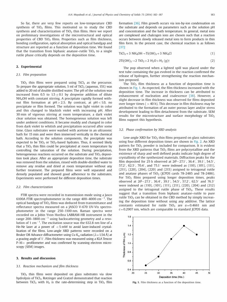
The TiO2 film thickness as a function of deposition time isshown in Fig. 1. As expected, the film thickness increased with thedeposition time. The increase in thickness can be attributed toenhancement of nucleation and coalescence [38]. However, aslight decrease in film thickness was observed for films depositedover longer times (440 h). This decrease in film thickness may beattributed to the formation of an outer porous layer and/or stressdevelopment leading to film detachment from the substrate. SEMresults for the microstructure and surface morphology of TiO2
films support this hypothesis.
3.2. Phase confirmation by XRD analysis
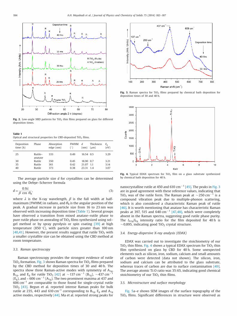
Low-angle XRD for TiO2 thin films prepared on glass substratesusing four different deposition times are shown in Fig. 2. An XRDpattern for TiO2 powder is included for comparison. It is evidentfrom the XRD patterns that TiO2 films are polycrystalline and theexistence of sharp and well defined peaks indicate high degree ofcrystallinity of the synthesized materials. Diffraction peaks for thefilm deposited for 25 h observed at 2θ�27.11, 36.41, 39.11, 54.51,57.21, 62.51, 70.41, and 75.11 were indexed as (110), (101), (111),(211), (220), (204), (220) and (215) assigned to tetragonal rutileand anatase phases of TiO2 (JCPDS cards 78-2485 and 78-2486).For TiO2 films prepared using longer deposition times, peaksobserved at 2θ�27.11, 36.41, 39.11, 54.51, 57.21, 62.51 and 76.31were indexed as (110), (101), (111), (211), (220), (204) and (212)assigned to the tetragonal rutile phase of TiO2. These resultssuggest that a transition from biphasic anatase–rutile to purerutile TiO2 can be obtained in the CBD method by simply increas-ing the deposition time without using any additive. The latticeconstants estimated for rutile TiO2 are a¼0.4661 nm andc¼0.2907 nm, which are comparable to standard JCPDS data.
Fig. 1. Film thickness as a function of the deposition time.
A.H. Mayabadi et al. / Journal of Physics and Chemistry of Solids 75 (2014) 182–187 183
The average particle size d for crystallites can be determinedusing the Debye–Scherrer formula
d¼ 0:9λβ cos θB
; ð3Þ
where λ is the X-ray wavelength, β is the full width at half-maximum (FWHM) in radians, and θB is the angular position of thepeak. A gradual increase in particle size from 16 to 23 nm wasobserved with increasing deposition time (Table 1). Several groupshave observed a transition from mixed anatase–rutile phase topure rutile phase on annealing of TiO2 films synthesized using sol–gel method or by spray pyrolysis or spin coating [39] at hightemperature (850 1C), with particle sizes greater than 100 nm[40,41]. However, the present results suggest that rutile TiO2 witha smaller crystallite size can be obtained using the CBD method atroom temperature.
3.3. Raman spectroscopy
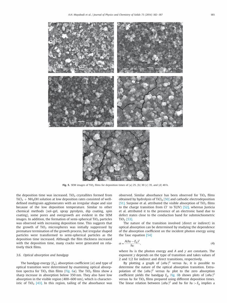
Raman spectroscopy provides the strongest evidence of rutileTiO2 formation. Fig. 3 shows Raman spectra for TiO2 films preparedby the CBD method for deposition times of 30 and 40 h. Thespectra show three Raman-active modes with symmetry of A1g,B1g, and Eg for rutile TiO2 [42] at �137 cm�1 (B1g), �437 cm�1
(Eg), and ~ 606 cm�1 (A1g). The two prominent maxima at 437 and606 cm–1 are comparable to those found for single-crystal rutileTiO2 [43]. Begun et al. reported intense Raman peaks for bulkrutile at 235, 443 and 610 cm–1 corresponding to B1g, Eg and A1g
active modes, respectively [44]. Ma et al. reported strong peaks for
nanocrystalline rutile at 450 and 610 cm�1 [45]. The peaks in Fig. 3are in good agreement with these reference values, indicating thatTiO2 was of the rutile form. The Raman peak at �250 cm�1 is acompound vibration peak due to multiple-phonon scattering,which is also considered a characteristic Raman peak of rutile[46]. It is worth mentioning that anatase has characteristic Ramanpeaks at 397, 515 and 640 cm�1 [47,48], which were completelyabsent in the Raman spectra, suggesting good rutile phase purity.The IA1g/IEg intensity ratio for the film deposited for 40 h is�0.895, indicating good TiO2 crystal structure.
3.4. Energy-dispersive X-ray analysis (EDAX)
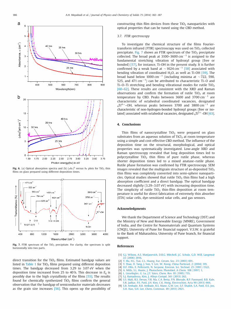
EDAX was carried out to investigate the stoichiometry of ourTiO2 thin films. Fig. 4 shows a typical EDAX spectrum for TiO2 thinfilm synthesized on glass by CBD for 40 h. Some unexpectedelements such as silicon, iron, sodium, calcium and small amountsof carbon were detected (data not shown). The silicon, iron,sodium and calcium can be attributed to the glass substrate,whereas traces of carbon are due to surface contamination [49].The average atomic Ti:O ratio was 35:65, indicating good chemicalstoichiometry of our TiO2 thin films.
3.5. Microstructure and surface morphology
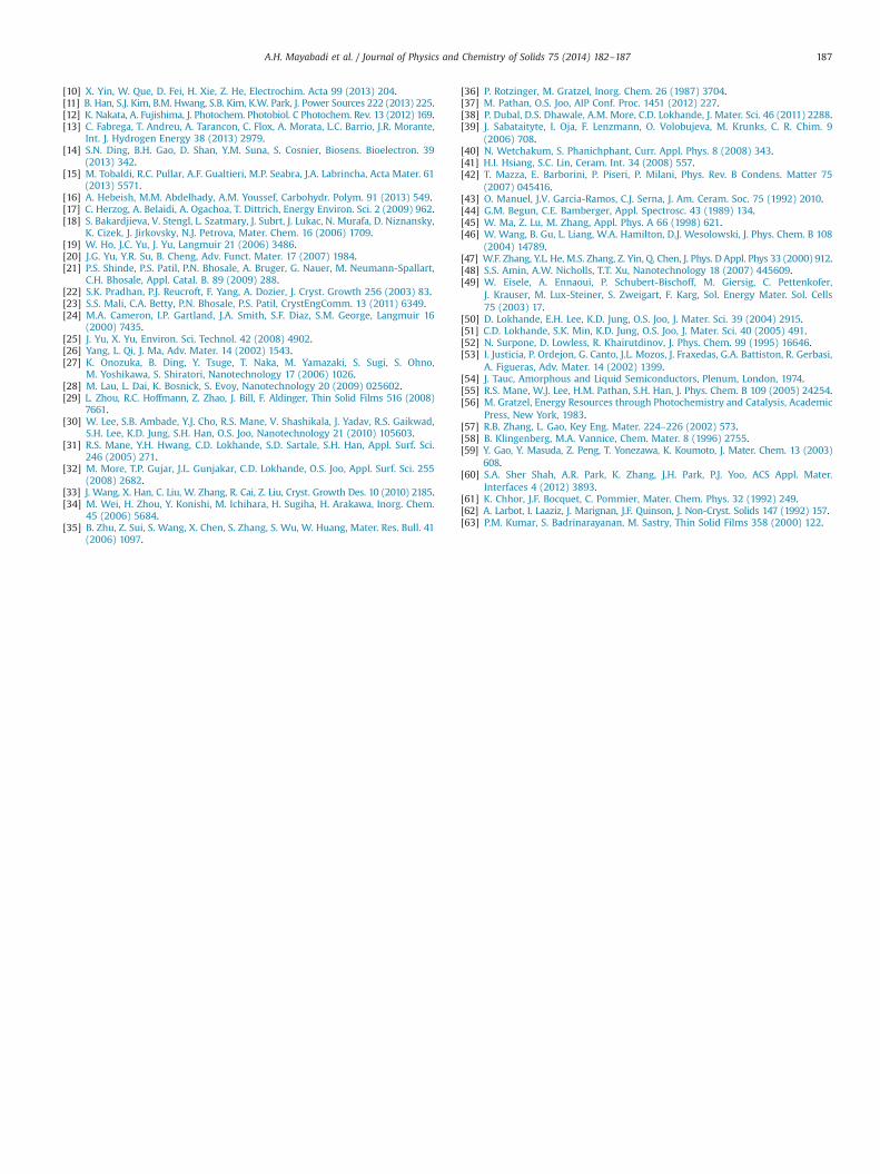
Fig. 5a–e shows SEM images of the surface topography of theTiO2 films. Significant differences in structure were observed as
Fig. 2. Low-angle XRD patterns for TiO2 thin films prepared on glass for differentdeposition times.
Table 1Optical and structural properties for CBD-deposited TiO2 films.
Depositiontime (h)
Phase Absorptionedge (nm)
FWHM(1)
d(nm)
Thickness(μm)
Eg(eV)
25 Rutile–anatase
333 0.49 16.54 0.5 3.29
30 Rutile 350 0.45 18.90 0.7 3.2135 Rutile 361 0.42 21.07 1.1 3.1440 Rutile 373 0.38 23.31 1.4 3.07
Fig. 3. Raman spectra for TiO2 films prepared by chemical bath deposition fordeposition times of 30 and 40 h.
Fig. 4. Typical EDAX spectrum for TiO2 film on a glass substrate synthesizedby chemical bath deposition for 40 h.
A.H. Mayabadi et al. / Journal of Physics and Chemistry of Solids 75 (2014) 182–187184
the deposition time was increased. TiO2 crystallites formed fromTiCl3 þ NH4OH solution at low deposition rates consisted of well-defined multigrain agglomerates with an irregular shape and sizebecause of the low deposition temperature. Similar to otherchemical methods (sol–gel, spray pyrolysis, dip coating, spincoating), some pores and overgrowth are evident in the SEMimages. In addition, the formation of semi-spherical TiO2 particleswas observed with increasing deposition time. This suggests thatthe growth of TiO2 microspheres was initially suppressed bypremature termination of the growth process, but irregular shapedparticles were transformed to semi-spherical particles as thedeposition time increased. Although the film thickness increasedwith the deposition time, many cracks were generated on rela-tively thick films.
3.6. Optical absorption and bandgap
The bandgap energy (Eg), absorption coefficient (α) and type ofoptical transition were determined by examining optical absorp-tion spectra for TiO2 thin films (Fig. 6a). The TiO2 films show asharp increase in absorption below 350 nm. They also have lowabsorption in the visible region (400–600 nm), which is character-istic of TiO2 [43]. In this region, tailing of the absorbance was
observed. Similar absorbance has been observed for TiO2 filmsobtained by hydrolysis of TiCl4 [50] and cathodic electrodeposition[51]. Surpone et al. attributed the visible absorption of TiO2 filmsto the charge transition from Cl– to Ti(IV) [52], whereas Justiciaet al. attributed it to the presence of an electronic band due todefect states close to the conduction band for substoichiometricTiO2 [53].
The nature of the transition involved (direct or indirect) inoptical absorption can be determined by studying the dependenceof the absorption coefficient on the incident photon energy usingthe Tauc equation [54]
α¼ Aðhν�EgÞγhν
; ð4Þ
where hν is the photon energy and A and γ are constants. Theexponent γ depends on the type of transition and takes values of2 and 1/2 for indirect and direct transitions, respectively.
By plotting a graph of (αhν)2 versus hν, it is possible todetermine the nature of the optical absorption transition. Extra-polation of the (αhν)2 versus hν plot to the zero absorptioncoefficient yields the bandgap Eg. Fig. 6b shows plots of (αhν)2
versus hν for TiO2 films prepared using different deposition times.The linear relation between (αhν)2 and hν for hν4Eg implies a
Fig. 5. SEM images of TiO2 films for deposition times of (a) 25, (b) 30 (c) 35, and (d) 40 h.
A.H. Mayabadi et al. / Journal of Physics and Chemistry of Solids 75 (2014) 182–187 185
direct transition for the TiO2 films. Estimated bandgap values arelisted in Table 1 for TiO2 films prepared using different depositiontimes. The bandgap decreased from 3.29 to 3.07 eV when thedeposition time increased from 25 to 40 h. This decrease in Eg ispossibly due to the high crystallinity of the films [55]. The resultsfound for chemically synthesized TiO2 films confirm the generalobservation that the bandgap of semiconductor materials decreasesas the grain size increases [56]. This opens up the possibility of
constructing thin film devices from these TiO2 nanoparticles withoptical properties that can be tuned using the CBD method.
3.7. FTIR spectroscopy
To investigate the chemical structure of the films Fourier-transform infrared (FTIR) spectroscopy was used on TiO2 collectedprecipitate. Fig. 7 shows an FTIR spectrum of the TiO2 precipitatecollected. The broad peak at 3100–3600 cm�1 is assigned to thefundamental stretching vibration of hydroxyl group (free orbonded) [57], for instance, Ti-OH in the present study. It is furtherconfirmed by a weak band at �1624 cm�1 [58] associated withbending vibration of coordinated H2O, as well as Ti-OH [59]. Thebroad band below 1000 cm�1 (including minima at �722, 590,525, and 471 cm�1) can be attributed to characteristic Ti–O andTi–O–Ti stretching and bending vibrational modes for rutile TiO2
[60–62]. These results are consistent with the XRD and Ramanobservations and confirm the formation of rutile TiO2 at roomtemperature by CBD. Peaks between 3600 and 3700 cm�1 arecharacteristic of octahedral coordinated vacancies, designated4Ti4þ–OH, whereas peaks between 3700 and 3800 cm�1 arecharacteristic of non-hydrogen-bonded hydroxyl groups (free or iso-lated) associated with octahedral vacancies, designated 6Ti3þ-OH [63].
4. Conclusions
Thin films of nanocrystalline TiO2 were prepared on glasssubstrates from an aqueous solution of TiCl3 at room temperatureusing a simple and cost-effective CBD method. The influence of thedeposition time on the structural, morphological, and opticalproperties was systematically investigated. Low-angle XRD andRaman spectroscopy revealed that long deposition times led topolycrystalline TiO2 thin films of pure rutile phase, whereasshorter deposition times led to a mixed anatase–rutile phase.Rutile phase formation was confirmed by FTIR spectroscopy. SEMimages revealed that the multigrain structure of as-deposited TiO2
thin films was completely converted into semi-sphere nanoparti-cles. Optical studies showed that rutile TiO2 thin films had a highabsorption coefficient and a direct bandgap. The optical bandgapdecreased slightly (3.29–3.07 eV) with increasing deposition time.The simplicity of rutile TiO2 thin-film deposition at room tem-perature is useful for direct fabrication of extremely thin absorber(ETA) solar cells, dye-sensitized solar cells, and gas sensors.
Acknowledgments
We thank the Department of Science and Technology (DST) andthe Ministry of New and Renewable Energy (MNRE), Governmentof India, and the Centre for Nanomaterials and Quantum Systems(CNQS), University of Pune for financial support. V.S.W. is gratefulto the Bank of Maharashtra, University of Pune branch, for financialsupport.
References
[1] G.J. Wilson, A.S. Matijasevich, D.R.G. Mitchell, J.C. Schulz, G.D. Will, Langmuir22 (2006) 2016.
[2] Y. Hu, H.L. Tsai, C.L. Huang, Eur. Ceram. Soc. 23 (2003) 691.[3] Y. Shao, D. Tang, J. Sun, Y. Lee, W. Xiong, China Particuol. 2 (2004) 119.[4] D.F. Ollis, E. Pellizzetti, N. Serpone, Environ. Sci. Technol. 25 (1991) 1522.[5] A. Mills, S.L. Hunte, J. Photochem. Photobiol. A Chem. 108 (1997) 1.[6] L. Linsebigler, G. Lu, J.T. Yates, Chem. Rev. 95 (1995) 735.[7] S.J. Ramadossa, Kim, J. Alloys Compd. 561 (2013) 262.[8] S.S. Mali, R.S. Devan, Y.R. Ma, C.A. Betty, P.N. Bhosale, R.P. Panmand, B.B. Kale,
S.R. Jadkar, P.S. Patil, J.H. Kim, C.K. Hong, Electrochim. Acta 90 (2013) 666.[9] S.B. Ambade, R.B. Ambade, R.S. Mane, G.W. Lee, S.F. Shaikh, S.A. Patil, O.S. Joo,
S.H. Han, S.H. Lee, Chem. Commun. 49 (2013) 2921.
Fig. 6. (a) Optical absorption spectra and (b) (αhν)2 versus hν plots for TiO2 thinfilms on glass prepared using different deposition times.
Fig. 7. FTIR spectrum of the TiO2 precipitate. For clarity, the spectrum is splithorizontally into two parts.
A.H. Mayabadi et al. / Journal of Physics and Chemistry of Solids 75 (2014) 182–187186
[10] X. Yin, W. Que, D. Fei, H. Xie, Z. He, Electrochim. Acta 99 (2013) 204.[11] B. Han, S.J. Kim, B.M. Hwang, S.B. Kim, K.W. Park, J. Power Sources 222 (2013) 225.[12] K. Nakata, A. Fujishima, J. Photochem. Photobiol. C Photochem. Rev. 13 (2012) 169.[13] C. Fabrega, T. Andreu, A. Tarancon, C. Flox, A. Morata, L.C. Barrio, J.R. Morante,
Int. J. Hydrogen Energy 38 (2013) 2979.[14] S.N. Ding, B.H. Gao, D. Shan, Y.M. Suna, S. Cosnier, Biosens. Bioelectron. 39
(2013) 342.[15] M. Tobaldi, R.C. Pullar, A.F. Gualtieri, M.P. Seabra, J.A. Labrincha, Acta Mater. 61
(2013) 5571.[16] A. Hebeish, M.M. Abdelhady, A.M. Youssef, Carbohydr. Polym. 91 (2013) 549.[17] C. Herzog, A. Belaidi, A. Ogachoa, T. Dittrich, Energy Environ. Sci. 2 (2009) 962.[18] S. Bakardjieva, V. Stengl, L. Szatmary, J. Subrt, J. Lukac, N. Murafa, D. Niznansky,
K. Cizek, J. Jirkovsky, N.J. Petrova, Mater. Chem. 16 (2006) 1709.[19] W. Ho, J.C. Yu, J. Yu, Langmuir 21 (2006) 3486.[20] J.G. Yu, Y.R. Su, B. Cheng, Adv. Funct. Mater. 17 (2007) 1984.[21] P.S. Shinde, P.S. Patil, P.N. Bhosale, A. Bruger, G. Nauer, M. Neumann-Spallart,
C.H. Bhosale, Appl. Catal. B. 89 (2009) 288.[22] S.K. Pradhan, P.J. Reucroft, F. Yang, A. Dozier, J. Cryst. Growth 256 (2003) 83.[23] S.S. Mali, C.A. Betty, P.N. Bhosale, P.S. Patil, CrystEngComm. 13 (2011) 6349.[24] M.A. Cameron, I.P. Gartland, J.A. Smith, S.F. Diaz, S.M. George, Langmuir 16
(2000) 7435.[25] J. Yu, X. Yu, Environ. Sci. Technol. 42 (2008) 4902.[26] Yang, L. Qi, J. Ma, Adv. Mater. 14 (2002) 1543.[27] K. Onozuka, B. Ding, Y. Tsuge, T. Naka, M. Yamazaki, S. Sugi, S. Ohno,
M. Yoshikawa, S. Shiratori, Nanotechnology 17 (2006) 1026.[28] M. Lau, L. Dai, K. Bosnick, S. Evoy, Nanotechnology 20 (2009) 025602.[29] L. Zhou, R.C. Hoffmann, Z. Zhao, J. Bill, F. Aldinger, Thin Solid Films 516 (2008)
7661.[30] W. Lee, S.B. Ambade, Y.J. Cho, R.S. Mane, V. Shashikala, J. Yadav, R.S. Gaikwad,
S.H. Lee, K.D. Jung, S.H. Han, O.S. Joo, Nanotechnology 21 (2010) 105603.[31] R.S. Mane, Y.H. Hwang, C.D. Lokhande, S.D. Sartale, S.H. Han, Appl. Surf. Sci.
246 (2005) 271.[32] M. More, T.P. Gujar, J.L. Gunjakar, C.D. Lokhande, O.S. Joo, Appl. Surf. Sci. 255
(2008) 2682.[33] J. Wang, X. Han, C. Liu, W. Zhang, R. Cai, Z. Liu, Cryst. Growth Des. 10 (2010) 2185.[34] M. Wei, H. Zhou, Y. Konishi, M. Ichihara, H. Sugiha, H. Arakawa, Inorg. Chem.
45 (2006) 5684.[35] B. Zhu, Z. Sui, S. Wang, X. Chen, S. Zhang, S. Wu, W. Huang, Mater. Res. Bull. 41
(2006) 1097.
[36] P. Rotzinger, M. Gratzel, Inorg. Chem. 26 (1987) 3704.[37] M. Pathan, O.S. Joo, AIP Conf. Proc. 1451 (2012) 227.[38] P. Dubal, D.S. Dhawale, A.M. More, C.D. Lokhande, J. Mater. Sci. 46 (2011) 2288.[39] J. Sabataityte, I. Oja, F. Lenzmann, O. Volobujeva, M. Krunks, C. R. Chim. 9
(2006) 708.[40] N. Wetchakum, S. Phanichphant, Curr. Appl. Phys. 8 (2008) 343.[41] H.I. Hsiang, S.C. Lin, Ceram. Int. 34 (2008) 557.[42] T. Mazza, E. Barborini, P. Piseri, P. Milani, Phys. Rev. B Condens. Matter 75
(2007) 045416.[43] O. Manuel, J.V. Garcia-Ramos, C.J. Serna, J. Am. Ceram. Soc. 75 (1992) 2010.[44] G.M. Begun, C.E. Bamberger, Appl. Spectrosc. 43 (1989) 134.[45] W. Ma, Z. Lu, M. Zhang, Appl. Phys. A 66 (1998) 621.[46] W. Wang, B. Gu, L. Liang, W.A. Hamilton, D.J. Wesolowski, J. Phys. Chem. B 108
(2004) 14789.[47] W.F. Zhang, Y.L. He, M.S. Zhang, Z. Yin, Q. Chen, J. Phys. D Appl. Phys 33 (2000) 912.[48] S.S. Amin, A.W. Nicholls, T.T. Xu, Nanotechnology 18 (2007) 445609.[49] W. Eisele, A. Ennaoui, P. Schubert-Bischoff, M. Giersig, C. Pettenkofer,
J. Krauser, M. Lux-Steiner, S. Zweigart, F. Karg, Sol. Energy Mater. Sol. Cells75 (2003) 17.
[50] D. Lokhande, E.H. Lee, K.D. Jung, O.S. Joo, J. Mater. Sci. 39 (2004) 2915.[51] C.D. Lokhande, S.K. Min, K.D. Jung, O.S. Joo, J. Mater. Sci. 40 (2005) 491.[52] N. Surpone, D. Lowless, R. Khairutdinov, J. Phys. Chem. 99 (1995) 16646.[53] I. Justicia, P. Ordejon, G. Canto, J.L. Mozos, J. Fraxedas, G.A. Battiston, R. Gerbasi,
A. Figueras, Adv. Mater. 14 (2002) 1399.[54] J. Tauc, Amorphous and Liquid Semiconductors, Plenum, London, 1974.[55] R.S. Mane, W.J. Lee, H.M. Pathan, S.H. Han, J. Phys. Chem. B 109 (2005) 24254.[56] M. Gratzel, Energy Resources through Photochemistry and Catalysis, Academic
Press, New York, 1983.[57] R.B. Zhang, L. Gao, Key Eng. Mater. 224–226 (2002) 573.[58] B. Klingenberg, M.A. Vannice, Chem. Mater. 8 (1996) 2755.[59] Y. Gao, Y. Masuda, Z. Peng, T. Yonezawa, K. Koumoto, J. Mater. Chem. 13 (2003)
608.[60] S.A. Sher Shah, A.R. Park, K. Zhang, J.H. Park, P.J. Yoo, ACS Appl. Mater.
Interfaces 4 (2012) 3893.[61] K. Chhor, J.F. Bocquet, C. Pommier, Mater. Chem. Phys. 32 (1992) 249.[62] A. Larbot, I. Laaziz, J. Marignan, J.F. Quinson, J. Non-Cryst. Solids 147 (1992) 157.[63] P.M. Kumar, S. Badrinarayanan, M. Sastry, Thin Solid Films 358 (2000) 122.
A.H. Mayabadi et al. / Journal of Physics and Chemistry of Solids 75 (2014) 182–187 187
Related Documents


![CLAYS, CLAY MINERALS AND CORDIERITE CERAMICS - A … · Clays, clay minerals and cordierite ceramics – a review Ceramics – Silikáty 59 (4) 331-340 (2015) 333 plastic [17]. The](https://static.cupdf.com/doc/110x72/5cb2c45c88c99331158c06cf/clays-clay-minerals-and-cordierite-ceramics-a-clays-clay-minerals-and-cordierite.jpg)