March 2016 DocID025038 Rev 2 1/59 59 AN4338 Application note EVLSTNRG-170W: 170 W SMPS with digitally controlled PFC and resonant LLC stage based on the STNRG388A Introduction This application note describes the characteristics and features of a 170 W, wide input mains range, power factor corrected, evaluation board for evaluating the STNRG388A digital controller in off-line power conversion applications such as digital industrial power supplies. The solution implements a PFC stage followed by a resonant LLC stage supporting up to 170 W with multiple output rails: a high power 24 V (6 A) channel for the main application, 1 auxiliary 12 V (2 A) for the controller and an always-on 5 V (2 A) standby. The STNRG388A power conversion dedicated peripherals (SMEDs) offer the flexibility to drive the PFC in transition mode (DCM-CCM boundary) while the resonant LLC is controlled with timeshift control (TSC). In parallel to managing the two conversion stages, the STNRG388A device guarantees all the protections required by the application as well as implementing the advanced anti-capacitive protection. Thanks to the digital core of the STNRG388A device, it is also possible to monitor, control and debug the EVLSTNRG-170W board via a convenient HyperTerminal control. The EVLSTNRG-170W evaluation kit (Figure 1) is comprised of a power board, accommodating power circuits and gate drivers L6382D, and a control card with a digital control CORE based on the STNRG388A device. The control module receives status signals from the power circuit and provides control signals to the power board. Two different control cards are provided: “Slim”: this board shows how small a real application could be “Debug”: this board allows to easily monitor all STNRG388A signals, in order to understand the operation of the system or debugging a new code. Figure 1. EVLSTNRG-170W with “slim“ control board configuration www.st.com

Welcome message from author
This document is posted to help you gain knowledge. Please leave a comment to let me know what you think about it! Share it to your friends and learn new things together.
Transcript

March 2016 DocID025038 Rev 2 1/59
59
AN4338Application note
EVLSTNRG-170W: 170 W SMPS with digitally controlled PFC andresonant LLC stage based on the STNRG388A
Introduction
This application note describes the characteristics and features of a 170 W, wide input mains range, power factor corrected, evaluation board for evaluating the STNRG388A digital controller in off-line power conversion applications such as digital industrial power supplies. The solution implements a PFC stage followed by a resonant LLC stage supporting up to 170 W with multiple output rails: a high power 24 V (6 A) channel for the main application, 1 auxiliary 12 V (2 A) for the controller and an always-on 5 V (2 A) standby.
The STNRG388A power conversion dedicated peripherals (SMEDs) offer the flexibility to drive the PFC in transition mode (DCM-CCM boundary) while the resonant LLC is controlled with timeshift control (TSC). In parallel to managing the two conversion stages, the STNRG388A device guarantees all the protections required by the application as well as implementing the advanced anti-capacitive protection. Thanks to the digital core of the STNRG388A device, it is also possible to monitor, control and debug the EVLSTNRG-170W board via a convenient HyperTerminal control.
The EVLSTNRG-170W evaluation kit (Figure 1) is comprised of a power board, accommodating power circuits and gate drivers L6382D, and a control card with a digital control CORE based on the STNRG388A device. The control module receives status signals from the power circuit and provides control signals to the power board. Two different control cards are provided:
“Slim”: this board shows how small a real application could be
“Debug”: this board allows to easily monitor all STNRG388A signals, in order to understand the operation of the system or debugging a new code.
Figure 1. EVLSTNRG-170W with “slim“ control board configuration
www.st.com

Contents AN4338
2/59 DocID025038 Rev 2
Contents
1 Main characteristics and circuit description . . . . . . . . . . . . . . . . . . . . . 5
1.1 Boost PFC stage features . . . . . . . . . . . . . . . . . . . . . . . . . . . . . . . . . . . . . 6
1.2 LLC resonant HB converter features . . . . . . . . . . . . . . . . . . . . . . . . . . . . . 6
1.3 Flyback converter features . . . . . . . . . . . . . . . . . . . . . . . . . . . . . . . . . . . . . 6
1.4 Related documents . . . . . . . . . . . . . . . . . . . . . . . . . . . . . . . . . . . . . . . . . . 6
1.5 HW configuration . . . . . . . . . . . . . . . . . . . . . . . . . . . . . . . . . . . . . . . . . . . . 7
1.6 Digital PFC description . . . . . . . . . . . . . . . . . . . . . . . . . . . . . . . . . . . . . . . . 8
1.7 Digital LLC description . . . . . . . . . . . . . . . . . . . . . . . . . . . . . . . . . . . . . . . .11
2 Efficiency measurement . . . . . . . . . . . . . . . . . . . . . . . . . . . . . . . . . . . . . 14
3 PFC performance . . . . . . . . . . . . . . . . . . . . . . . . . . . . . . . . . . . . . . . . . . 15
4 Functional checks . . . . . . . . . . . . . . . . . . . . . . . . . . . . . . . . . . . . . . . . . . 17
4.1 Power factor corrector stage . . . . . . . . . . . . . . . . . . . . . . . . . . . . . . . . . . 17
4.2 Resonant stage . . . . . . . . . . . . . . . . . . . . . . . . . . . . . . . . . . . . . . . . . . . . 19
4.3 Dynamic load operation and output voltage regulation . . . . . . . . . . . . . . 20
4.4 Cross regulation . . . . . . . . . . . . . . . . . . . . . . . . . . . . . . . . . . . . . . . . . . . . 22
4.5 Startup . . . . . . . . . . . . . . . . . . . . . . . . . . . . . . . . . . . . . . . . . . . . . . . . . . . 23
4.6 Mains dips . . . . . . . . . . . . . . . . . . . . . . . . . . . . . . . . . . . . . . . . . . . . . . . . 25
4.7 Mains ripple rejection . . . . . . . . . . . . . . . . . . . . . . . . . . . . . . . . . . . . . . . . 26
5 Conducted emission pre-compliance test . . . . . . . . . . . . . . . . . . . . . . 28
Appendix A Electrical diagrams . . . . . . . . . . . . . . . . . . . . . . . . . . . . . . . . . . . . . . 29
Appendix B Bill of materials . . . . . . . . . . . . . . . . . . . . . . . . . . . . . . . . . . . . . . . . . 37
Board revision . . . . . . . . . . . . . . . . . . . . . . . . . . . . . . . . . . . . . . . . . . . . . . . . . . . . . . 57
Revision history . . . . . . . . . . . . . . . . . . . . . . . . . . . . . . . . . . . . . . . . . . . . . . . . . . . . 58

DocID025038 Rev 2 3/59
AN4338 List of tables
59
List of tables
Table 1. PFC signals description . . . . . . . . . . . . . . . . . . . . . . . . . . . . . . . . . . . . . . . . . . . . . . . . . . . . 9Table 2. LLC signals description. . . . . . . . . . . . . . . . . . . . . . . . . . . . . . . . . . . . . . . . . . . . . . . . . . . . 13Table 3. Overall efficiency measured at different AC input voltages . . . . . . . . . . . . . . . . . . . . . . . . 14Table 4. PFC PF and THD . . . . . . . . . . . . . . . . . . . . . . . . . . . . . . . . . . . . . . . . . . . . . . . . . . . . . . . . 16Table 5. Bill of materials EVLSTNRG-170W “power board” . . . . . . . . . . . . . . . . . . . . . . . . . . . . . . . 37Table 6. Bill of materials EVLSTNRG-170W “STNRG388A debug control board” . . . . . . . . . . . . . . 48Table 7. Bill of materials EVLSTNRG-170W “STNRG388A slim control board”. . . . . . . . . . . . . . . . 54Table 8. Document revision history . . . . . . . . . . . . . . . . . . . . . . . . . . . . . . . . . . . . . . . . . . . . . . . . . 58
List of figures AN4338
4/59 DocID025038 Rev 2
List of figures
Figure 1. EVLSTNRG-170W with “slim“ control board configuration . . . . . . . . . . . . . . . . . . . . . . . . . . 1Figure 2. EVLSTNRG-170W with “debug” control board connected . . . . . . . . . . . . . . . . . . . . . . . . . . 8Figure 3. PFC block diagram and signals description . . . . . . . . . . . . . . . . . . . . . . . . . . . . . . . . . . . . 10Figure 4. Enhanced constant on-time PFC boost inductor current profile . . . . . . . . . . . . . . . . . . . . . 11Figure 5. LLC block diagram and signals description . . . . . . . . . . . . . . . . . . . . . . . . . . . . . . . . . . . . 13Figure 6. Time-shift concept . . . . . . . . . . . . . . . . . . . . . . . . . . . . . . . . . . . . . . . . . . . . . . . . . . . . . . . 14Figure 7. EN61000-3-2 compliance at 230 V ac - 50 Hz, full load . . . . . . . . . . . . . . . . . . . . . . . . . . . 16Figure 8. JEITA-MITI compliance at 100 V ac - 50 Hz, full load . . . . . . . . . . . . . . . . . . . . . . . . . . . . 16Figure 9. EN61000-3-2 compliance at 230 V ac - 50 Hz, 75 W . . . . . . . . . . . . . . . . . . . . . . . . . . . . . 16Figure 10. JEITA-MITI compliance at 100 V ac - 50 Hz, 75 W . . . . . . . . . . . . . . . . . . . . . . . . . . . . . . 16Figure 11. Input voltage and current at 115 V ac - full load . . . . . . . . . . . . . . . . . . . . . . . . . . . . . . . . . 17Figure 12. Input voltage and current at 230 V ac - full load . . . . . . . . . . . . . . . . . . . . . . . . . . . . . . . . . 17Figure 13. PFC Vds and inductor current at 115 V ac - 60 Hz - full load . . . . . . . . . . . . . . . . . . . . . . . 18Figure 14. PFC Vds and inductor current at 115 V ac - 60 Hz - full load - detail . . . . . . . . . . . . . . . . . 18Figure 15. PFC Vds and inductor current at 230 V ac - 50 Hz - full load . . . . . . . . . . . . . . . . . . . . . . . 19Figure 16. PFC Vds and inductor current at 230 V ac - 50 Hz - full load - detail . . . . . . . . . . . . . . . . . 19Figure 17. PFC signals at 115 V ac - 60 Hz - full load . . . . . . . . . . . . . . . . . . . . . . . . . . . . . . . . . . . . . 19Figure 18. PFC signals - line transient 115 V ac to 230 V ac - 60 Hz - full load . . . . . . . . . . . . . . . . . 19Figure 19. Resonant stage waveforms, full load . . . . . . . . . . . . . . . . . . . . . . . . . . . . . . . . . . . . . . . . . 20Figure 20. Adaptive dead time . . . . . . . . . . . . . . . . . . . . . . . . . . . . . . . . . . . . . . . . . . . . . . . . . . . . . . . 20Figure 21. Adaptive dead time - HB rising edge . . . . . . . . . . . . . . . . . . . . . . . . . . . . . . . . . . . . . . . . . 21Figure 22. Adaptive dead time - HB falling edge . . . . . . . . . . . . . . . . . . . . . . . . . . . . . . . . . . . . . . . . . 21Figure 23. 12 V load transition at 115 V ac - 60 Hz . . . . . . . . . . . . . . . . . . . . . . . . . . . . . . . . . . . . . . . 22Figure 24. 12 V transition no-load to full load at 115 V ac - 60 Hz. . . . . . . . . . . . . . . . . . . . . . . . . . . . 22Figure 25. 24 V load transition at 115 V ac - 60 Hz . . . . . . . . . . . . . . . . . . . . . . . . . . . . . . . . . . . . . . . 22Figure 26. 24 V transition no-load to full load at 115 V ac - 60 Hz. . . . . . . . . . . . . . . . . . . . . . . . . . . . 22Figure 27. 24 V load transition at 115 V ac - 60 Hz - cross regulation on 12 V . . . . . . . . . . . . . . . . . . 23Figure 28. 12 V load transition at 115 V ac - 60 Hz - cross regulation on 24 V . . . . . . . . . . . . . . . . . . 23Figure 29. Startup at full load and 115 V ac - 60 Hz by ON/OFF signal . . . . . . . . . . . . . . . . . . . . . . . 24Figure 30. Startup at full load and 230 V ac - 50 Hz by ON/OFF signal - detail. . . . . . . . . . . . . . . . . . 24Figure 31. Resonant stage safe startup at full load . . . . . . . . . . . . . . . . . . . . . . . . . . . . . . . . . . . . . . . 25Figure 32. Turn-off at full load and 115 V ac - 60 Hz by ON/OFF signal . . . . . . . . . . . . . . . . . . . . . . . 25Figure 33. Turn-off at full load and 230 V ac - 50 Hz by ON/OFF signal - detail . . . . . . . . . . . . . . . . . 25Figure 34. One and half cycle (25 ms) mains dip at full load and 115 V ac - 60Hz . . . . . . . . . . . . . . . 26Figure 35. One and half cycle (30 ms) mains dip at full load and 230 V ac - 50 Hz . . . . . . . . . . . . . . 26Figure 36. LLC input voltage ripple rejection at full load - +12 Vout measurement . . . . . . . . . . . . . . . 27Figure 37. LLC input voltage ripple rejection at full load - +24 Vout measurement . . . . . . . . . . . . . . . 27Figure 38. Output voltages ripple and noise with infinite persistence . . . . . . . . . . . . . . . . . . . . . . . . . 28Figure 39. Output voltages ripple and noise with maximum resolution (2 ns/pt - sync. with mains) . . 28Figure 40. CE peak and average measurement 230 V - phase wire . . . . . . . . . . . . . . . . . . . . . . . . . . 29Figure 41. CE peak and average measurement 115 V - phase wire . . . . . . . . . . . . . . . . . . . . . . . . . . 29Figure 42. Main board electrical diagram. . . . . . . . . . . . . . . . . . . . . . . . . . . . . . . . . . . . . . . . . . . . . . . 30Figure 43. Electrical diagram of dead time block . . . . . . . . . . . . . . . . . . . . . . . . . . . . . . . . . . . . . . . . 31Figure 44. Electrical diagram of debug control board - controller . . . . . . . . . . . . . . . . . . . . . . . . . . . . 32Figure 45. Electrical diagram of debug control board - connections . . . . . . . . . . . . . . . . . . . . . . . . . . 33Figure 46. Electrical diagram of debug control board - power and interfaces . . . . . . . . . . . . . . . . . . . 34Figure 47. Electrical diagram of slim control board - controller . . . . . . . . . . . . . . . . . . . . . . . . . . . . . . 35Figure 48. Electrical diagram of slim control board - connections . . . . . . . . . . . . . . . . . . . . . . . . . . . . 36
DocID025038 Rev 2 5/59
AN4338 Main characteristics and circuit description
59
1 Main characteristics and circuit description
The main features of the SMPS are listed here below:
Universal input mains range: 90 264 V ac - frequency 45 65 Hz
Full load power 170 W
Output voltage 1: 24 V ± 5% at 6 A for backlight and audio supply
Output voltage 2: 12 V ± 3% at 2 A for panel supply
Output voltage 3: 5 V ± 2% at 2 A for microprocessor supply
Mains harmonics: according to EN61000-3-2 Class-D or JEITA-MITI Class-D
Standby mains consumption: at 230 V ac < 150 mW with 50 mW load
Overall efficiency at full load: better than 90% at full load
EMI: according to EN55022-Class-B
Safety: according to EN60950
Power board size: 195 x 115 mm, 25 mm max. components height from PCB
Control board size: “debug” 88 x 118 mm, “slim” 25 x 76 mm
Power board PCB: dual layers, 35 µm, mixed PTH/SMT
Control board PCB: four layers, 35 µm, mixed PTH/SMT
The circuit is composed of two sections:
1. A 10 W standby based on the VIPER27L, a high-voltage switcher for off-line applications. This auxiliary converter delivers 5 V/2 A and is dedicated to supply the TV microprocessor, the IR receiver, the logic and supervisory circuitry, as well as the control devices of the main converter.
2. The main converter composed of a front-end PFC and a LLC resonant converter, both controlled by the STNRG388A digital controller. The PFC stage delivers 400 V constant voltage and acts as a pre-regulator for both the LLC stage and the standby supply; the LLC resonant converter delivers two output voltages, one dedicated to supply the TV panel and the other for the backlight and audio power amplifiers.
An external signal, referred to secondary ground, turns on and off the main converter.
The drive function for the discrete MOSFETs of the main converter is provided by the L6382D: this dedicated companion driver integrates also the high voltage startup generator and a precise reference voltage (3.3 V) able to provide up to 30 mA to supply the STNRG388A.
Main characteristics and circuit description AN4338
6/59 DocID025038 Rev 2
1.1 Boost PFC stage features
Digitally controlled PFC pre-regulator
Transition-mode (DCM-CCM boundary) operation with valley switching
Enhanced constant on-time control with line voltage feedforward
Valley skipping with valley lock and burst mode operation
OCP with LEB on current sense
Protections:
– Brownout
– Overvoltage
– Undervoltage
– Overcurrent
– Anti-continuous conduction mode
Programmable soft-start
Digital control loop with programmable PI frequency compensator
1.2 LLC resonant HB converter features
Time-shift control with min. and max. frequency limitation
Self-adjustable dead time
Protections:
– 2 levels overcurrent
– Overvoltage
– Anti-capacitive mode
Safe start and digitally adjustable soft-start
1.3 Flyback converter features
Fixed switching frequency (60 kHz) with frequency jittering
CCM - DCM operation according to mains voltage and load amount
1.4 Related documents
Additional information and details about firmware and the parameters setting can be found in the following documents:
UM1881 - EVLSTNRG-170W: user interface manual
UM1760 - STLUX™ SMED configurator 1.0
This evaluation board has been developed starting from the existing EVL170W-FTV evaluation board, based on full analog control. Its application note (AN3329) can be used to have a description and relevant waveforms of the standby supply.
Since that evaluation board refers to the same application and uses the same power components, it is a good means for comparison between the analog and digital performance.
DocID025038 Rev 2 7/59
AN4338 Main characteristics and circuit description
59
1.5 HW configuration
As already said, the EVLSTNRG-170W includes two different control boards. They work exactly in the same way, using the same STNRG388A resources and sharing the same FW. The “Slim” version has been thought to show the actual size of the digital control in a real application. Since its height is only 25 mm it is mounted vertically on the power board. Therefore the total footprint of the SMPS is the same of the power board.
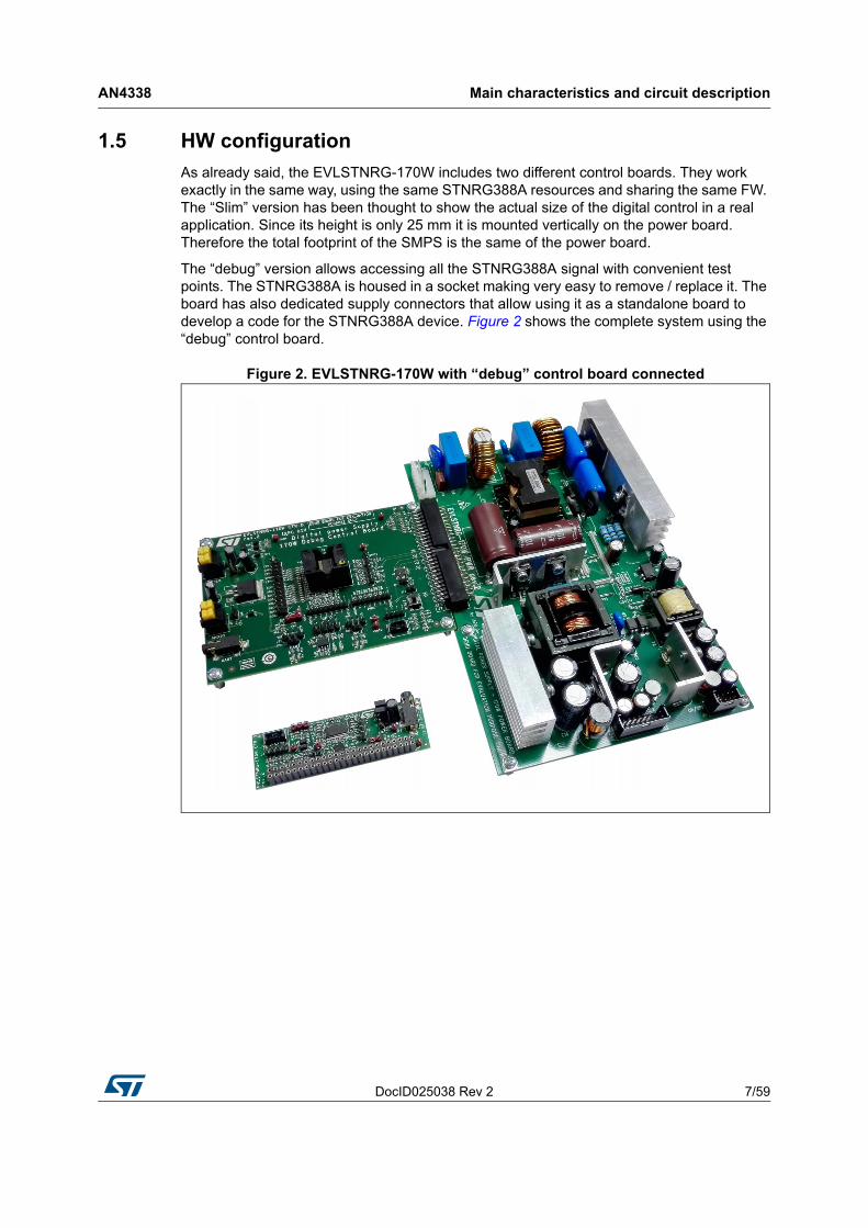
The “debug” version allows accessing all the STNRG388A signal with convenient test points. The STNRG388A is housed in a socket making very easy to remove / replace it. The board has also dedicated supply connectors that allow using it as a standalone board to develop a code for the STNRG388A device. Figure 2 shows the complete system using the “debug” control board.
Figure 2. EVLSTNRG-170W with “debug” control board connected
Main characteristics and circuit description AN4338
8/59 DocID025038 Rev 2
1.6 Digital PFC description
The PFC block diagram and STNRG388A pins used for PFC control are shown in Figure 3.
The gate drive signal for the power MOSFET is generated by two coupled SMEDs (“State Machine Event Driven”) and delivered through the gate driver L6382. The schematic also shows that four signals are sensed and opportunely scaled and conditioned. The PFC output voltage and AC line are sensed using the STNRG388A device. These signals are scaled to a range from 0 V to 1.25 V which corresponds to the ADC full scale. The demagnetization detection and power MOSFET current sensing for the cycle-by-cycle current limiting and current threshold detection are implemented with high speed analog comparators available in the STNRG388A.
The PFC operates in transition mode using a proprietary enhanced constant on-time technique. The on-time calculated by the voltage loop is kept constant for a given mains voltage and load condition during each line half cycle to obtain a good power factor and low harmonic content of the line current. The actual on-time is the sum of two times: the calculated one and that required for the current to reach a predefined threshold.
As a consequence, the on-time is not rigorously constant over a line half cycle.

DocID025038 Rev 2 9/59
AN4338 Main characteristics and circuit description
59
Figure 3. PFC block diagram and signals description
Table 1. PFC signals description
Name Description
Vin AC line monitor for: line synchronization, peak voltage sampling, brown-in/out
Vbulk Output voltage sampled for control loop PI and OVP, UVP
Vzcd Demagnetization detection from auxiliary for TM
Isen Current sensing for minimum current threshold and OCP
Main characteristics and circuit description AN4338
10/59 DocID025038 Rev 2
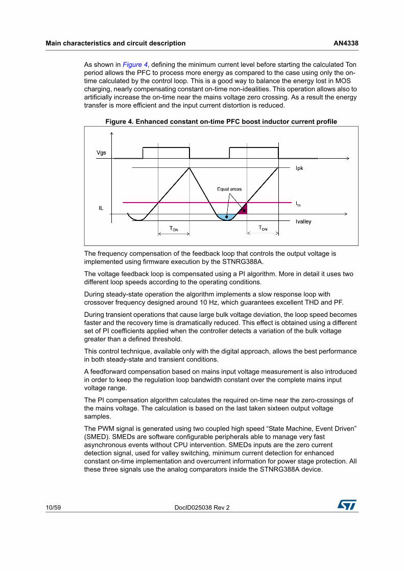
As shown in Figure 4, defining the minimum current level before starting the calculated Ton period allows the PFC to process more energy as compared to the case using only the on-time calculated by the control loop. This is a good way to balance the energy lost in MOS charging, nearly compensating constant on-time non-idealities. This operation allows also to artificially increase the on-time near the mains voltage zero crossing. As a result the energy transfer is more efficient and the input current distortion is reduced.
Figure 4. Enhanced constant on-time PFC boost inductor current profile
The frequency compensation of the feedback loop that controls the output voltage is implemented using firmware execution by the STNRG388A.
The voltage feedback loop is compensated using a PI algorithm. More in detail it uses two different loop speeds according to the operating conditions.
During steady-state operation the algorithm implements a slow response loop with crossover frequency designed around 10 Hz, which guarantees excellent THD and PF.
During transient operations that cause large bulk voltage deviation, the loop speed becomes faster and the recovery time is dramatically reduced. This effect is obtained using a different set of PI coefficients applied when the controller detects a variation of the bulk voltage greater than a defined threshold.
This control technique, available only with the digital approach, allows the best performance in both steady-state and transient conditions.
A feedforward compensation based on mains input voltage measurement is also introduced in order to keep the regulation loop bandwidth constant over the complete mains input voltage range.
The PI compensation algorithm calculates the required on-time near the zero-crossings of the mains voltage. The calculation is based on the last taken sixteen output voltage samples.
The PWM signal is generated using two coupled high speed “State Machine, Event Driven” (SMED). SMEDs are software configurable peripherals able to manage very fast asynchronous events without CPU intervention. SMEDs inputs are the zero current detection signal, used for valley switching, minimum current detection for enhanced constant on-time implementation and overcurrent information for power stage protection. All these three signals use the analog comparators inside the STNRG388A device.
DocID025038 Rev 2 11/59
AN4338 Main characteristics and circuit description
59
In critical condition, such as when the mains voltage approaches the PFC DC output, a proprietary algorithm guarantees that the “Continuous Conduction Mode” (CCM) is avoided.
The PFC can be operated in valley skipping and burst mode for improved efficiency at low output loads.
Valley skipping condition is directly managed by properly configured SMEDs states. If the calculated on-time is lower than a minimum configurable thresholds, the system inserts valley skipping, up to three valleys.
The system continuously checks that the PFC output voltage is under a reference value. If the limit is exceeded, the PFC enters the burst mode switching off the MOS. As soon as the PFC output voltage goes below a recovery value, the PFC is restarted.
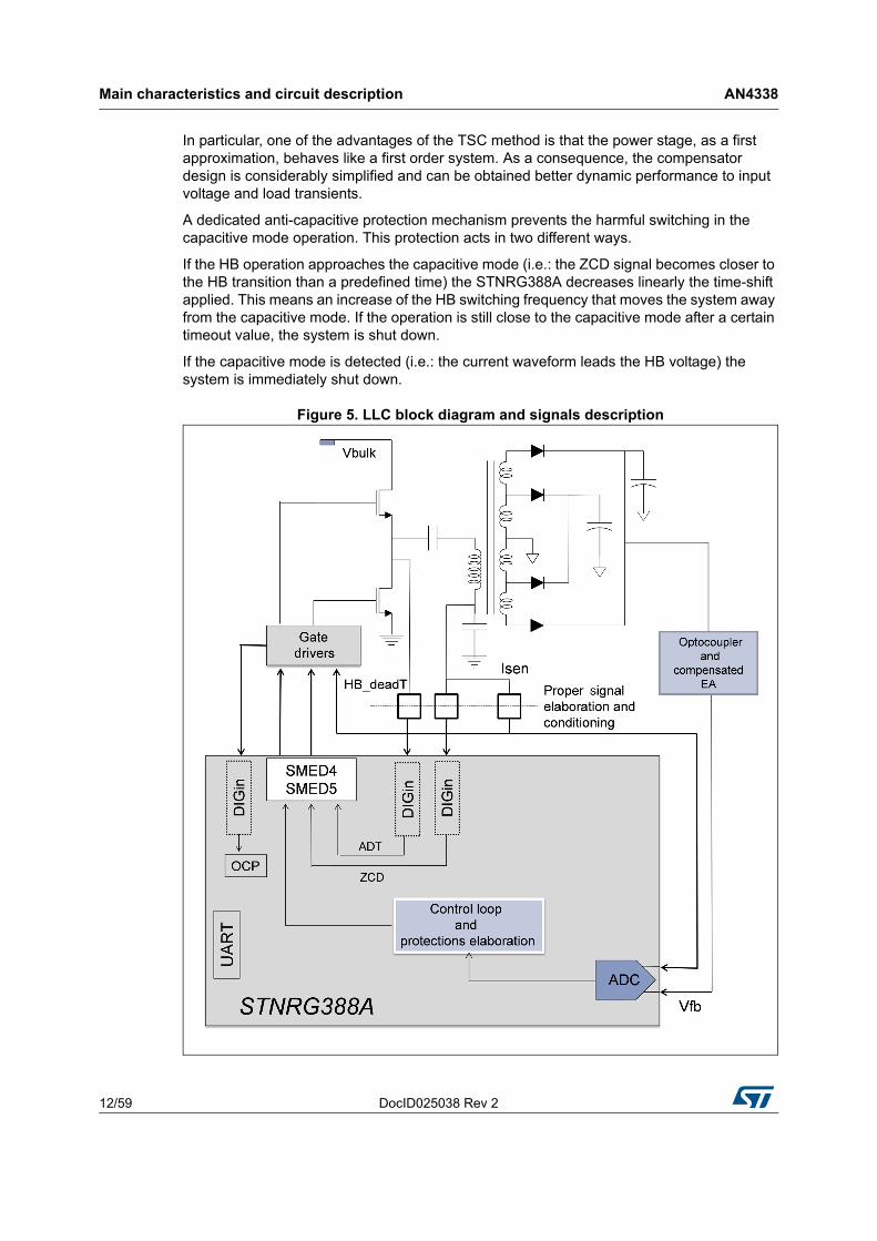
1.7 Digital LLC description
The LLC block diagram and STNRG388A pins used for LLC control are shown in Figure 5.
The schematic shows that the voltage feedback loop is implemented with a typical analog approach.
The loop is closed sensing both the output voltages with a circuit using a TL431 device modulating the current in the optocoupler diode.
The resulting feedback voltage is then sampled by the 10-bit ADC of the STNRG388A device.
In order to avoid half bridge (HB) switching noise effects, feedback voltage sampling instants are opportunely chosen by means of a dedicated ADC hardware triggering function.
The resonant stage average current is also sampled by the ADC to implement the first level of overcurrent protection (OCP). The intervention level is calculated taking into account the input voltage to the resonant stage. This approach allows limiting the maximum output power.
A second level OCP is implemented by an external comparator integrated in the L6382D IC which immediately stops the gate drives activity. A digital fault signal is sent to the STNRG388A that resets the system and attempts a restart after about 1 s. This protection has therefore an auto-restart behavior but can be easily modified into a latched one.
The HB power MOSFETs are driven by the controller's coupled SMEDs through the half bridge gate driver in the L6382. The input signals to the SMEDs include the resonant stage zero current detection signal and a signal for adaptive dead time management generated by a dedicated circuitry.
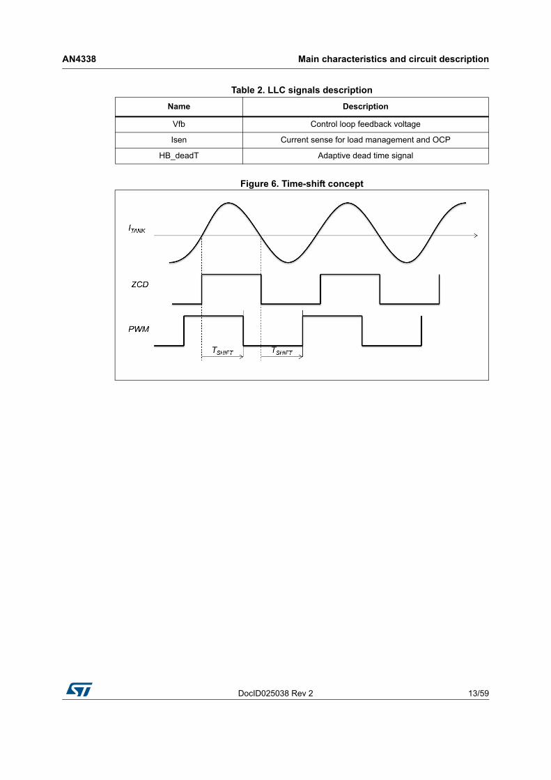
The zero current detection information is used to implement a proprietary control technique named “Time-Shift Control” (TSC). The TSC methodology consists in controlling the amount of time elapsing from a zero-crossing of the tank current to the switch-off of the MOSFET currently on, as shown in Figure 6. Conceptually, with TSC an inner loop is closed and the outer loop that regulates the output voltage provides the reference for the inner loop. This inner loop is completely managed by SMEDs using the zero current detection information.
Time-shift control outperforms the direct frequency control method.
Main characteristics and circuit description AN4338
12/59 DocID025038 Rev 2
In particular, one of the advantages of the TSC method is that the power stage, as a first approximation, behaves like a first order system. As a consequence, the compensator design is considerably simplified and can be obtained better dynamic performance to input voltage and load transients.
A dedicated anti-capacitive protection mechanism prevents the harmful switching in the capacitive mode operation. This protection acts in two different ways.
If the HB operation approaches the capacitive mode (i.e.: the ZCD signal becomes closer to the HB transition than a predefined time) the STNRG388A decreases linearly the time-shift applied. This means an increase of the HB switching frequency that moves the system away from the capacitive mode. If the operation is still close to the capacitive mode after a certain timeout value, the system is shut down.
If the capacitive mode is detected (i.e.: the current waveform leads the HB voltage) the system is immediately shut down.
Figure 5. LLC block diagram and signals description
DocID025038 Rev 2 13/59
AN4338 Main characteristics and circuit description
59
Figure 6. Time-shift concept
Table 2. LLC signals description
Name Description
Vfb Control loop feedback voltage
Isen Current sense for load management and OCP
HB_deadT Adaptive dead time signal
Efficiency measurement AN4338
14/59 DocID025038 Rev 2
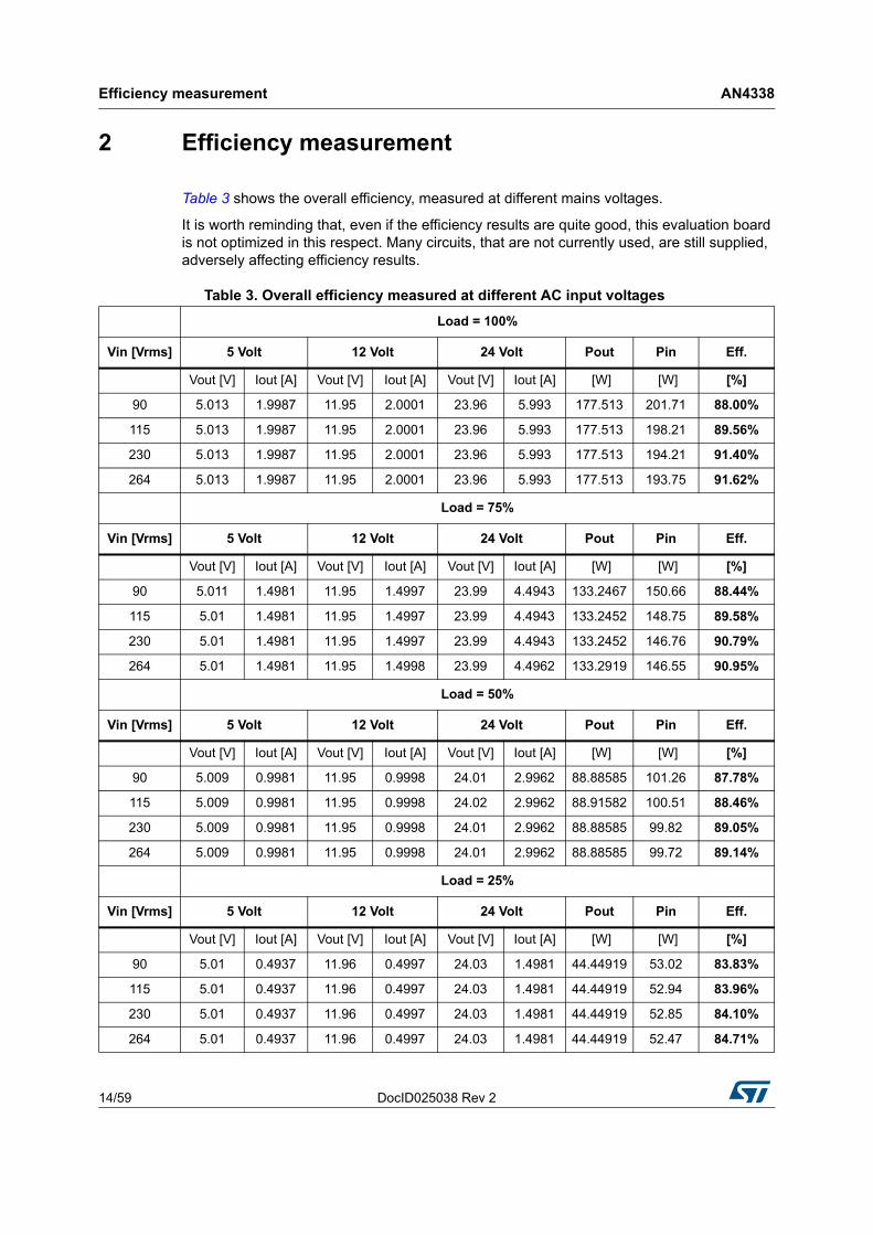
2 Efficiency measurement
Table 3 shows the overall efficiency, measured at different mains voltages.
It is worth reminding that, even if the efficiency results are quite good, this evaluation board is not optimized in this respect. Many circuits, that are not currently used, are still supplied, adversely affecting efficiency results.
Table 3. Overall efficiency measured at different AC input voltages
Load = 100%
Vin [Vrms] 5 Volt 12 Volt 24 Volt Pout Pin Eff.
Vout [V] Iout [A] Vout [V] Iout [A] Vout [V] Iout [A] [W] [W] [%]
90 5.013 1.9987 11.95 2.0001 23.96 5.993 177.513 201.71 88.00%
115 5.013 1.9987 11.95 2.0001 23.96 5.993 177.513 198.21 89.56%
230 5.013 1.9987 11.95 2.0001 23.96 5.993 177.513 194.21 91.40%
264 5.013 1.9987 11.95 2.0001 23.96 5.993 177.513 193.75 91.62%
Load = 75%
Vin [Vrms] 5 Volt 12 Volt 24 Volt Pout Pin Eff.
Vout [V] Iout [A] Vout [V] Iout [A] Vout [V] Iout [A] [W] [W] [%]
90 5.011 1.4981 11.95 1.4997 23.99 4.4943 133.2467 150.66 88.44%
115 5.01 1.4981 11.95 1.4997 23.99 4.4943 133.2452 148.75 89.58%
230 5.01 1.4981 11.95 1.4997 23.99 4.4943 133.2452 146.76 90.79%
264 5.01 1.4981 11.95 1.4998 23.99 4.4962 133.2919 146.55 90.95%
Load = 50%
Vin [Vrms] 5 Volt 12 Volt 24 Volt Pout Pin Eff.
Vout [V] Iout [A] Vout [V] Iout [A] Vout [V] Iout [A] [W] [W] [%]
90 5.009 0.9981 11.95 0.9998 24.01 2.9962 88.88585 101.26 87.78%
115 5.009 0.9981 11.95 0.9998 24.02 2.9962 88.91582 100.51 88.46%
230 5.009 0.9981 11.95 0.9998 24.01 2.9962 88.88585 99.82 89.05%
264 5.009 0.9981 11.95 0.9998 24.01 2.9962 88.88585 99.72 89.14%
Load = 25%
Vin [Vrms] 5 Volt 12 Volt 24 Volt Pout Pin Eff.
Vout [V] Iout [A] Vout [V] Iout [A] Vout [V] Iout [A] [W] [W] [%]
90 5.01 0.4937 11.96 0.4997 24.03 1.4981 44.44919 53.02 83.83%
115 5.01 0.4937 11.96 0.4997 24.03 1.4981 44.44919 52.94 83.96%
230 5.01 0.4937 11.96 0.4997 24.03 1.4981 44.44919 52.85 84.10%
264 5.01 0.4937 11.96 0.4997 24.03 1.4981 44.44919 52.47 84.71%
DocID025038 Rev 2 15/59
AN4338 PFC performance
59
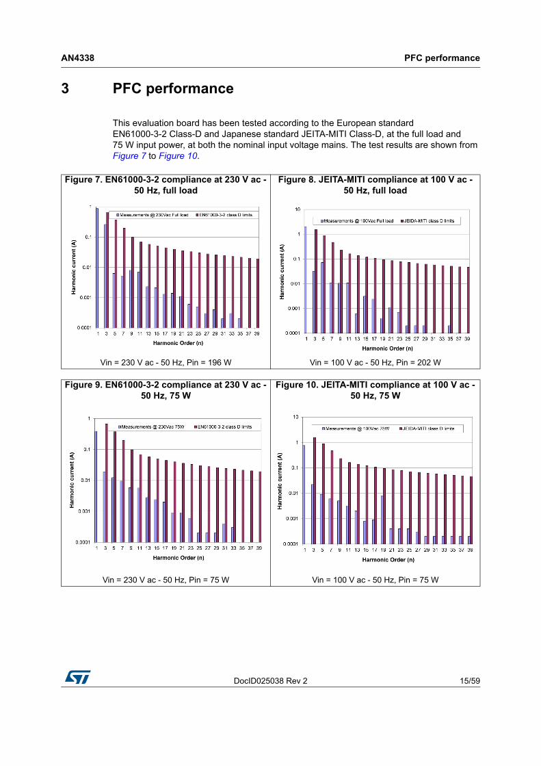
3 PFC performance
This evaluation board has been tested according to the European standard EN61000-3-2 Class-D and Japanese standard JEITA-MITI Class-D, at the full load and 75 W input power, at both the nominal input voltage mains. The test results are shown from Figure 7 to Figure 10.
Figure 7. EN61000-3-2 compliance at 230 V ac - 50 Hz, full load
Figure 8. JEITA-MITI compliance at 100 V ac - 50 Hz, full load
Vin = 230 V ac - 50 Hz, Pin = 196 W Vin = 100 V ac - 50 Hz, Pin = 202 W
Figure 9. EN61000-3-2 compliance at 230 V ac - 50 Hz, 75 W
Figure 10. JEITA-MITI compliance at 100 V ac - 50 Hz, 75 W
Vin = 230 V ac - 50 Hz, Pin = 75 W Vin = 100 V ac - 50 Hz, Pin = 75 W
PFC performance AN4338
16/59 DocID025038 Rev 2
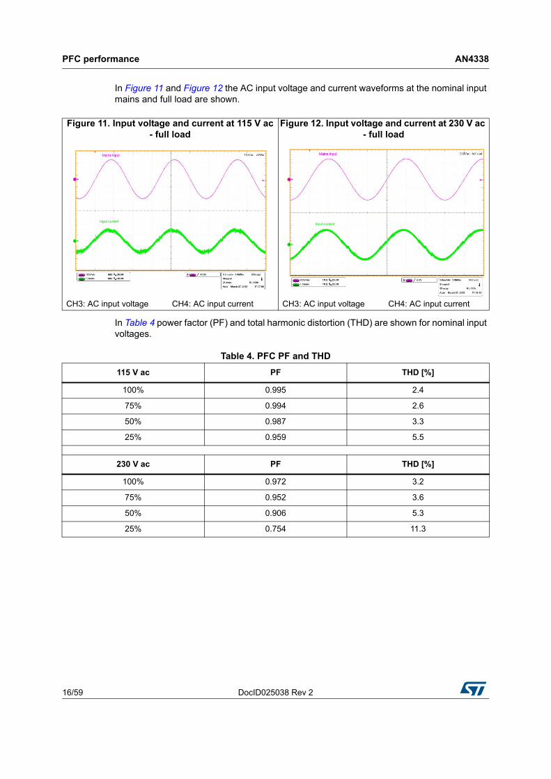
In Figure 11 and Figure 12 the AC input voltage and current waveforms at the nominal input mains and full load are shown.
In Table 4 power factor (PF) and total harmonic distortion (THD) are shown for nominal input voltages.
Figure 11. Input voltage and current at 115 V ac - full load
Figure 12. Input voltage and current at 230 V ac - full load
CH3: AC input voltage CH4: AC input current CH3: AC input voltage CH4: AC input current
Table 4. PFC PF and THD
115 V ac PF THD [%]
100% 0.995 2.4
75% 0.994 2.6
50% 0.987 3.3
25% 0.959 5.5
230 V ac PF THD [%]
100% 0.972 3.2
75% 0.952 3.6
50% 0.906 5.3
25% 0.754 11.3
DocID025038 Rev 2 17/59
AN4338 Functional checks
59
4 Functional checks
4.1 Power factor corrector stage
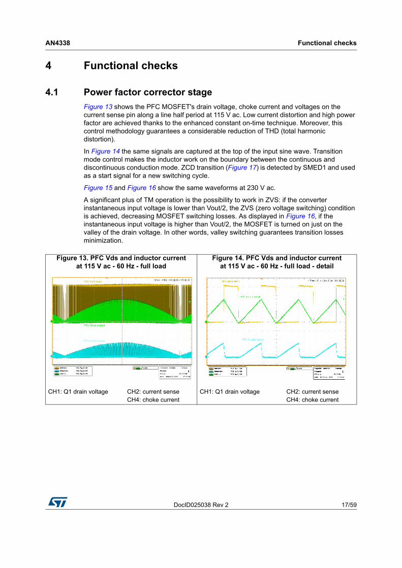
Figure 13 shows the PFC MOSFET's drain voltage, choke current and voltages on the current sense pin along a line half period at 115 V ac. Low current distortion and high power factor are achieved thanks to the enhanced constant on-time technique. Moreover, this control methodology guarantees a considerable reduction of THD (total harmonic distortion).
In Figure 14 the same signals are captured at the top of the input sine wave. Transition mode control makes the inductor work on the boundary between the continuous and discontinuous conduction mode. ZCD transition (Figure 17) is detected by SMED1 and used as a start signal for a new switching cycle.
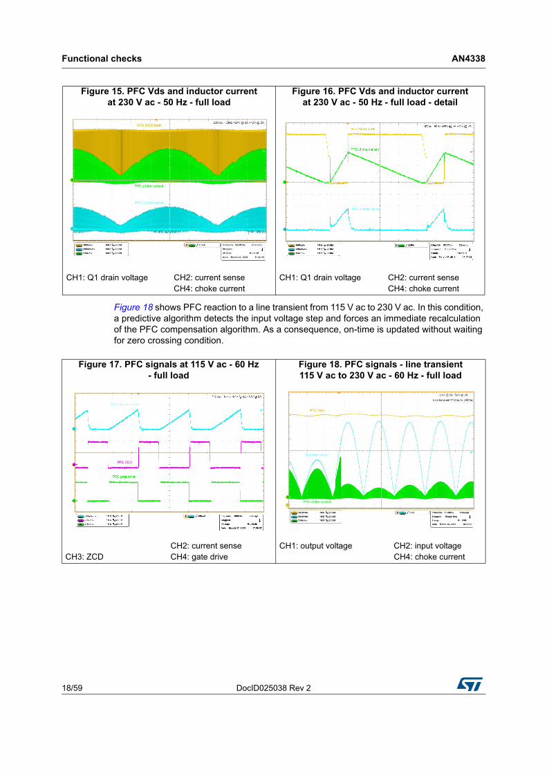
Figure 15 and Figure 16 show the same waveforms at 230 V ac.
A significant plus of TM operation is the possibility to work in ZVS: if the converter instantaneous input voltage is lower than Vout/2, the ZVS (zero voltage switching) condition is achieved, decreasing MOSFET switching losses. As displayed in Figure 16, if the instantaneous input voltage is higher than Vout/2, the MOSFET is turned on just on the valley of the drain voltage. In other words, valley switching guarantees transition losses minimization.
Figure 13. PFC Vds and inductor current at 115 V ac - 60 Hz - full load
Figure 14. PFC Vds and inductor current at 115 V ac - 60 Hz - full load - detail
CH1: Q1 drain voltage CH2: current sense CH1: Q1 drain voltage CH2: current sense CH4: choke current CH4: choke current
Functional checks AN4338
18/59 DocID025038 Rev 2
Figure 18 shows PFC reaction to a line transient from 115 V ac to 230 V ac. In this condition, a predictive algorithm detects the input voltage step and forces an immediate recalculation of the PFC compensation algorithm. As a consequence, on-time is updated without waiting for zero crossing condition.
Figure 15. PFC Vds and inductor current at 230 V ac - 50 Hz - full load
Figure 16. PFC Vds and inductor current at 230 V ac - 50 Hz - full load - detail
CH1: Q1 drain voltage CH2: current sense CH1: Q1 drain voltage CH2: current sense CH4: choke current CH4: choke current
Figure 17. PFC signals at 115 V ac - 60 Hz - full load
Figure 18. PFC signals - line transient 115 V ac to 230 V ac - 60 Hz - full load
CH2: current sense CH1: output voltage CH2: input voltage CH3: ZCD CH4: gate drive CH4: choke current
DocID025038 Rev 2 19/59
AN4338 Functional checks
59
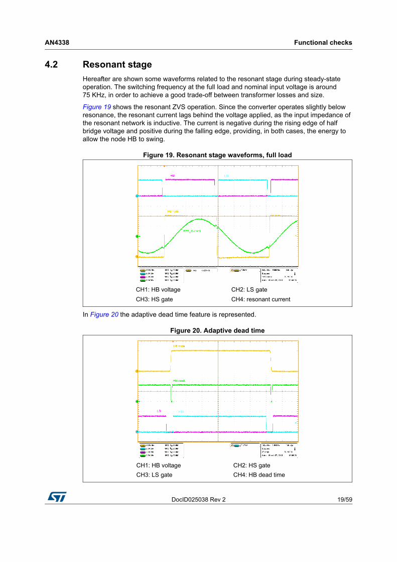
4.2 Resonant stage
Hereafter are shown some waveforms related to the resonant stage during steady-state operation. The switching frequency at the full load and nominal input voltage is around 75 KHz, in order to achieve a good trade-off between transformer losses and size.
Figure 19 shows the resonant ZVS operation. Since the converter operates slightly below resonance, the resonant current lags behind the voltage applied, as the input impedance of the resonant network is inductive. The current is negative during the rising edge of half bridge voltage and positive during the falling edge, providing, in both cases, the energy to allow the node HB to swing.
Figure 19. Resonant stage waveforms, full load
In Figure 20 the adaptive dead time feature is represented.
Figure 20. Adaptive dead time
CH2: LS gate
CH4: resonant current
CH1: HB voltage
CH3: HS gate
CH2: HS gate
CH4: HB dead time
CH1: HB voltage
CH3: LS gate
Functional checks AN4338
20/59 DocID025038 Rev 2
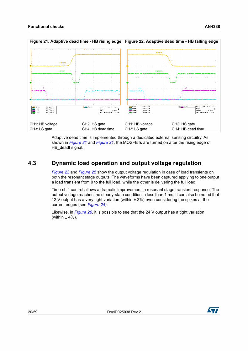
Adaptive dead time is implemented through a dedicated external sensing circuitry. As shown in Figure 21 and Figure 21, the MOSFETs are turned on after the rising edge of HB_deadt signal.
4.3 Dynamic load operation and output voltage regulation
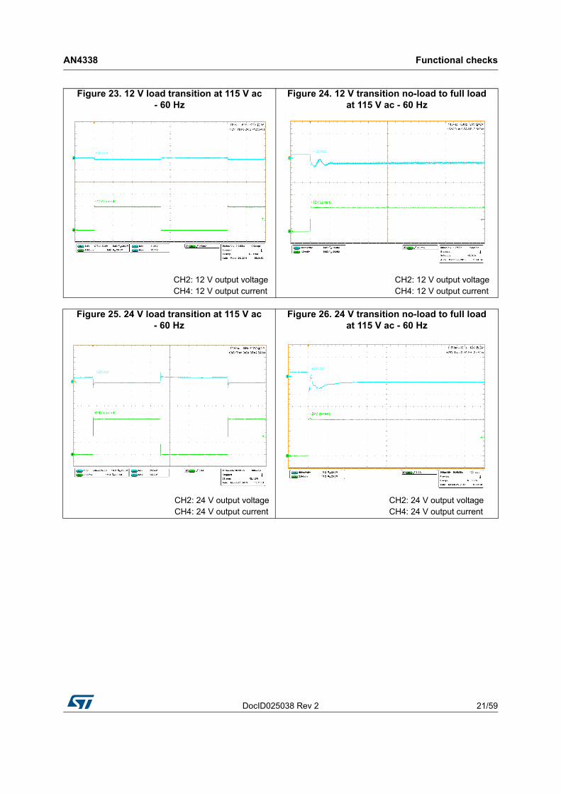
Figure 23 and Figure 25 show the output voltage regulation in case of load transients on both the resonant stage outputs. The waveforms have been captured applying to one output a load transient from 0 to the full load, while the other is delivering the full load.
Time-shift control allows a dramatic improvement in resonant stage transient response. The output voltage reaches the steady-state condition in less than 1 ms. It can also be noted that 12 V output has a very tight variation (within ± 3%) even considering the spikes at the current edges (see Figure 24).
Likewise, in Figure 26, it is possible to see that the 24 V output has a tight variation (within ± 4%).
Figure 21. Adaptive dead time - HB rising edge Figure 22. Adaptive dead time - HB falling edge
CH1: HB voltage CH2: HS gate CH1: HB voltage CH2: HS gateCH3: LS gate CH4: HB dead time CH3: LS gate CH4: HB dead time
DocID025038 Rev 2 21/59
AN4338 Functional checks
59
Figure 23. 12 V load transition at 115 V ac - 60 Hz
Figure 24. 12 V transition no-load to full load at 115 V ac - 60 Hz
CH2: 12 V output voltage CH2: 12 V output voltageCH4: 12 V output current CH4: 12 V output current
Figure 25. 24 V load transition at 115 V ac - 60 Hz
Figure 26. 24 V transition no-load to full load at 115 V ac - 60 Hz
CH2: 24 V output voltage CH2: 24 V output voltage CH4: 24 V output current CH4: 24 V output current

Functional checks AN4338
22/59 DocID025038 Rev 2
4.4 Cross regulation
Figure 27 and Figure 28 show the output voltage cross regulation with transient conditions similar to those of the test described above apart from the load step frequency, which is 300 Hz on one output, with the other one delivering the rated load. The transient response is so good that both outputs are able to reach the steady-state condition well before another load transition takes place.
s
Figure 27. 24 V load transition at 115 V ac - 60 Hz - cross regulation on 12 V
Figure 28. 12 V load transition at 115 V ac - 60 Hz - cross regulation on 24 V
CH2: 12 V output voltage CH2: 12 V output voltageCH3: 24 V output voltage CH4: output current CH3: 24 V output voltage CH4: output current

DocID025038 Rev 2 23/59
AN4338 Functional checks
59
4.5 Startup
Figure 29 and Figure 30 show waveforms during the startup at nominal voltages and the full load of the PFC and resonant stages. It is possible to note the sequence of the two stages; once the ON/OFF signal is asserted high, the voltage on C42 increases up to the Vcc turn-on threshold of the L6382D.
The driver, then, generates the supply voltage for the STNRG388A. At first the PFC is enabled, hereafter its output voltage starts increasing from the mains rectified peak voltage to its nominal value. Meanwhile the resonant stage is kept disabled. As soon as the PFC voltage reaches 380 V, the resonant starts to operate. Hence both the output voltages rise according to the soft-start and reach their nominal levels.
Figure 29. Startup at full load and 115 V ac - 60 Hz by ON/OFF signal
Figure 30. Startup at full load and 230 V ac - 50 Hz by ON/OFF signal - detail
CH1: PFC output voltage CH2: ON/OFF signal CH1: PFC output voltage CH2: ON/OFF signalCH3: 24 V output voltage CH4: 12 V output voltage CH3: 24 V output voltage CH4: 12 V output voltage

Functional checks AN4338
24/59 DocID025038 Rev 2
Figure 31 shows the details of the half bridge startup. It can be noted that the low-side gate drive starts first with a pulse of about 10 s, used to pre-charge the bootstrap capacitor. After a fixed delay of 40 s (used to let any possible oscillations to be completely damped), the half bridge starts its switching activity. The initial HB pulse is asymmetric as the duration of the high-side pulse is half that of the low-side one. The purpose of this operation is to prevent hard switching operation and flux imbalance. This startup sequence is implemented by means of a proper configuration of resonant SMEDs' timings that can be dynamically adjusted depending on the operating conditions of the resonant stage. As soon as the startup sequence is completed, SMEDs are immediately reconfigured to manage normal operation.
Figure 32 and Figure 33 show the PFC and resonant converter turn-off.
Figure 31. Resonant stage safe startup at full load
CH1: HB voltage
CH3: HS gate
CH2: LS gate
CH4: resonant current
Figure 32. Turn-off at full load and 115 V ac - 60 Hz by ON/OFF signal
Figure 33. Turn-off at full load and 230 V ac - 50 Hz by ON/OFF signal - detail
CH1: PFC output voltage CH2: ON/OFF signal CH1: PFC output voltage CH2: ON/OFF signalCH3: 24 V output voltage CH4: 12 V output voltage CH3: 24 V output voltage CH4:12 V output voltage
DocID025038 Rev 2 25/59
AN4338 Functional checks
59
4.6 Mains dips
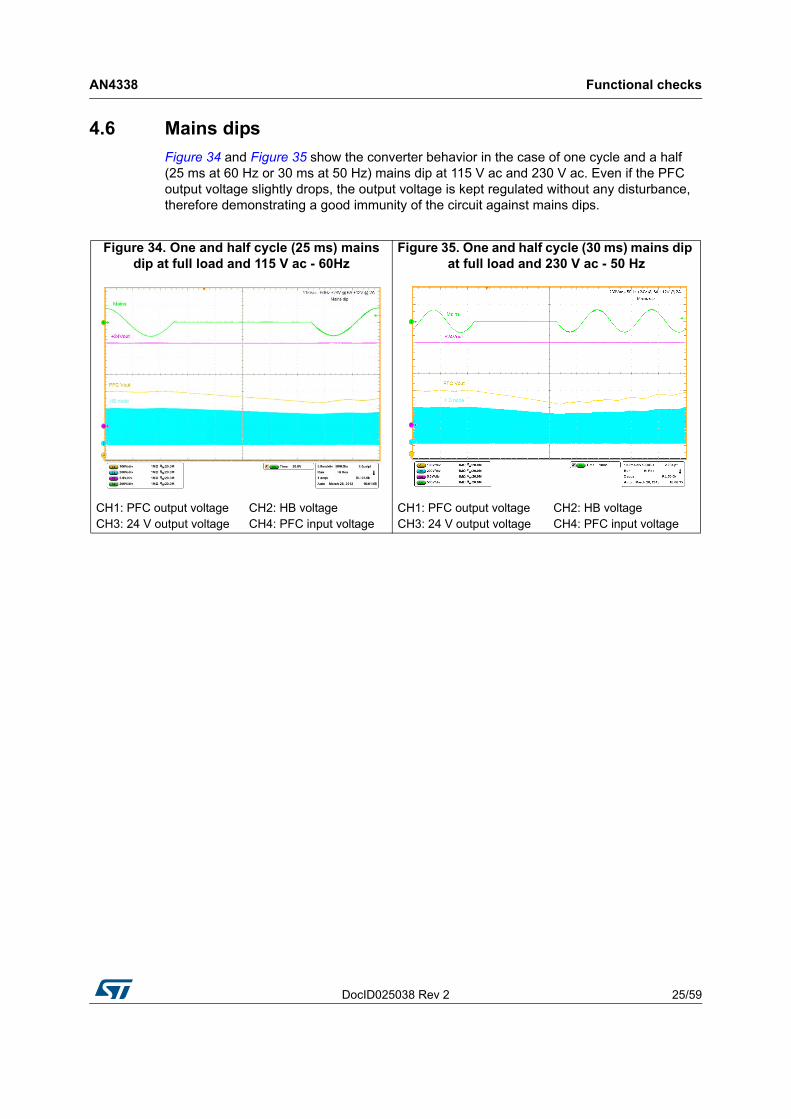
Figure 34 and Figure 35 show the converter behavior in the case of one cycle and a half (25 ms at 60 Hz or 30 ms at 50 Hz) mains dip at 115 V ac and 230 V ac. Even if the PFC output voltage slightly drops, the output voltage is kept regulated without any disturbance, therefore demonstrating a good immunity of the circuit against mains dips.
Figure 34. One and half cycle (25 ms) mains dip at full load and 115 V ac - 60Hz
Figure 35. One and half cycle (30 ms) mains dip at full load and 230 V ac - 50 Hz
CH1: PFC output voltage CH2: HB voltage CH1: PFC output voltage CH2: HB voltageCH3: 24 V output voltage CH4: PFC input voltage CH3: 24 V output voltage CH4: PFC input voltage
Functional checks AN4338
26/59 DocID025038 Rev 2
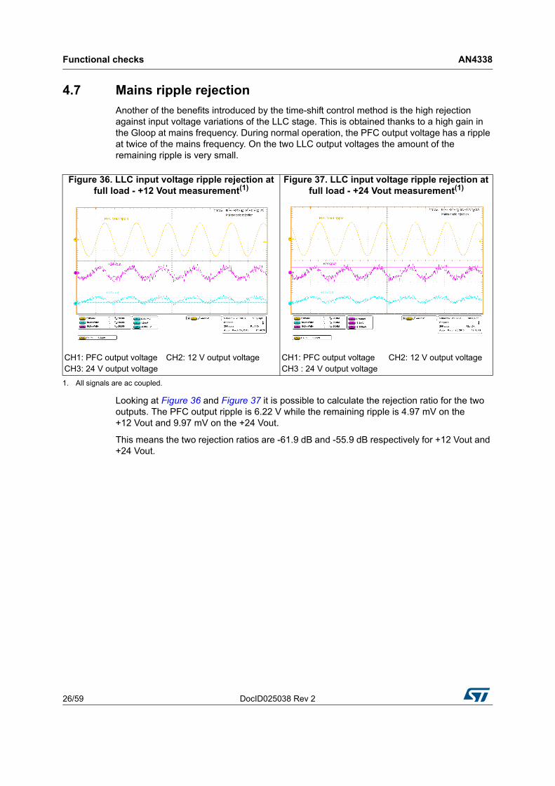
4.7 Mains ripple rejection
Another of the benefits introduced by the time-shift control method is the high rejection against input voltage variations of the LLC stage. This is obtained thanks to a high gain in the Gloop at mains frequency. During normal operation, the PFC output voltage has a ripple at twice of the mains frequency. On the two LLC output voltages the amount of the remaining ripple is very small.
Looking at Figure 36 and Figure 37 it is possible to calculate the rejection ratio for the two outputs. The PFC output ripple is 6.22 V while the remaining ripple is 4.97 mV on the +12 Vout and 9.97 mV on the +24 Vout.
This means the two rejection ratios are -61.9 dB and -55.9 dB respectively for +12 Vout and +24 Vout.
Figure 36. LLC input voltage ripple rejection at full load - +12 Vout measurement(1)
Figure 37. LLC input voltage ripple rejection at full load - +24 Vout measurement(1)
CH1: PFC output voltage CH2: 12 V output voltage CH1: PFC output voltage CH2: 12 V output voltageCH3: 24 V output voltage CH3 : 24 V output voltage
1. All signals are ac coupled.
DocID025038 Rev 2 27/59
AN4338 Functional checks
59
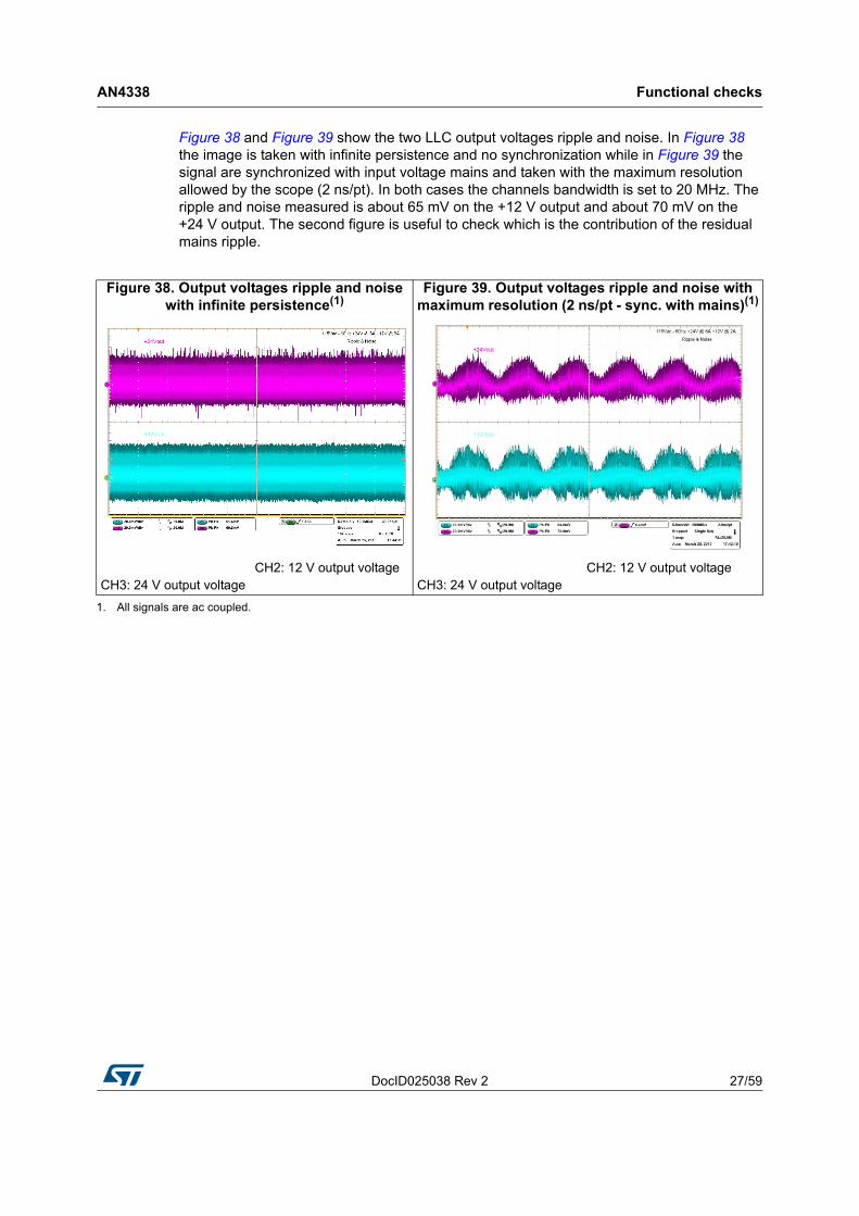
Figure 38 and Figure 39 show the two LLC output voltages ripple and noise. In Figure 38 the image is taken with infinite persistence and no synchronization while in Figure 39 the signal are synchronized with input voltage mains and taken with the maximum resolution allowed by the scope (2 ns/pt). In both cases the channels bandwidth is set to 20 MHz. The ripple and noise measured is about 65 mV on the +12 V output and about 70 mV on the +24 V output. The second figure is useful to check which is the contribution of the residual mains ripple.
Figure 38. Output voltages ripple and noise with infinite persistence(1)
Figure 39. Output voltages ripple and noise with maximum resolution (2 ns/pt - sync. with mains)(1)
CH2: 12 V output voltage CH2: 12 V output voltage CH3: 24 V output voltage CH3: 24 V output voltage
1. All signals are ac coupled.
Conducted emission pre-compliance test AN4338
28/59 DocID025038 Rev 2
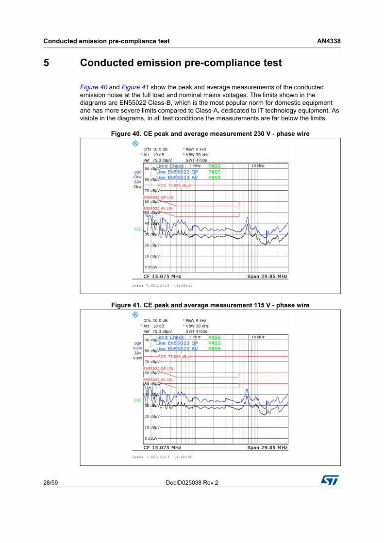
5 Conducted emission pre-compliance test
Figure 40 and Figure 41 show the peak and average measurements of the conducted emission noise at the full load and nominal mains voltages. The limits shown in the diagrams are EN55022 Class-B, which is the most popular norm for domestic equipment and has more severe limits compared to Class-A, dedicated to IT technology equipment. As visible in the diagrams, in all test conditions the measurements are far below the limits.
Figure 40. CE peak and average measurement 230 V - phase wire
Figure 41. CE peak and average measurement 115 V - phase wire

DocID025038 Rev 2 29/59
AN4338 Electrical diagrams
59
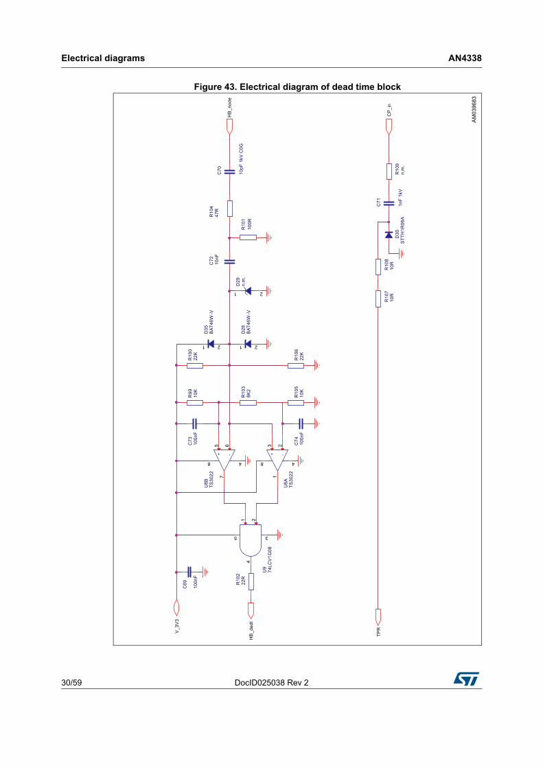
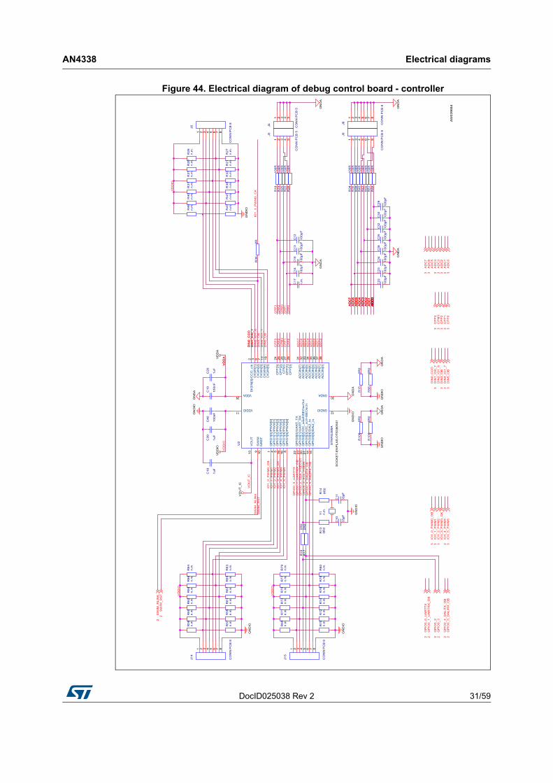
Appendix A Electrical diagrams
Figure 42. Main board electrical diagram
Electrical diagrams AN4338
30/59 DocID025038 Rev 2
Figure 43. Electrical diagram of dead time block
DocID025038 Rev 2 31/59
AN4338 Electrical diagrams
59
Figure 44. Electrical diagram of debug control board - controller
Electrical diagrams AN4338
32/59 DocID025038 Rev 2
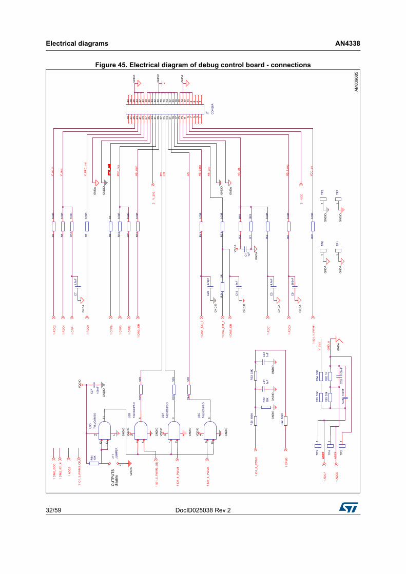
Figure 45. Electrical diagram of debug control board - connections
DocID025038 Rev 2 33/59
AN4338 Electrical diagrams
59
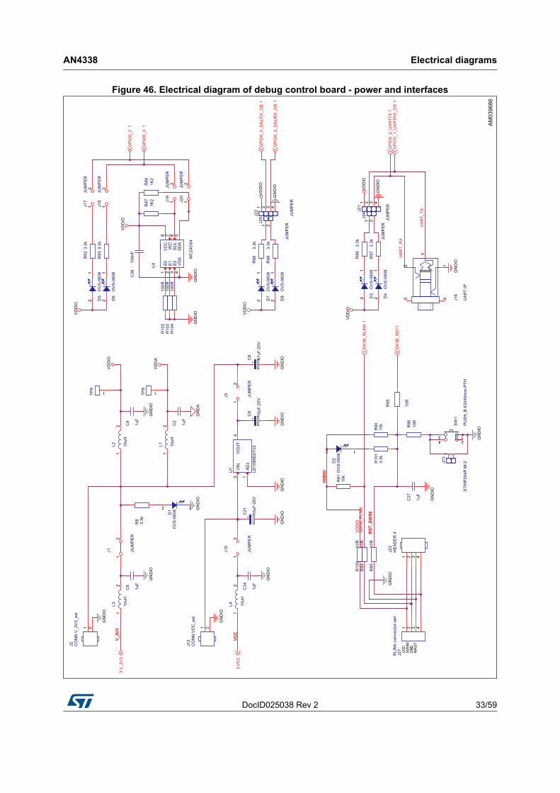
Figure 46. Electrical diagram of debug control board - power and interfaces
Electrical diagrams AN4338
34/59 DocID025038 Rev 2
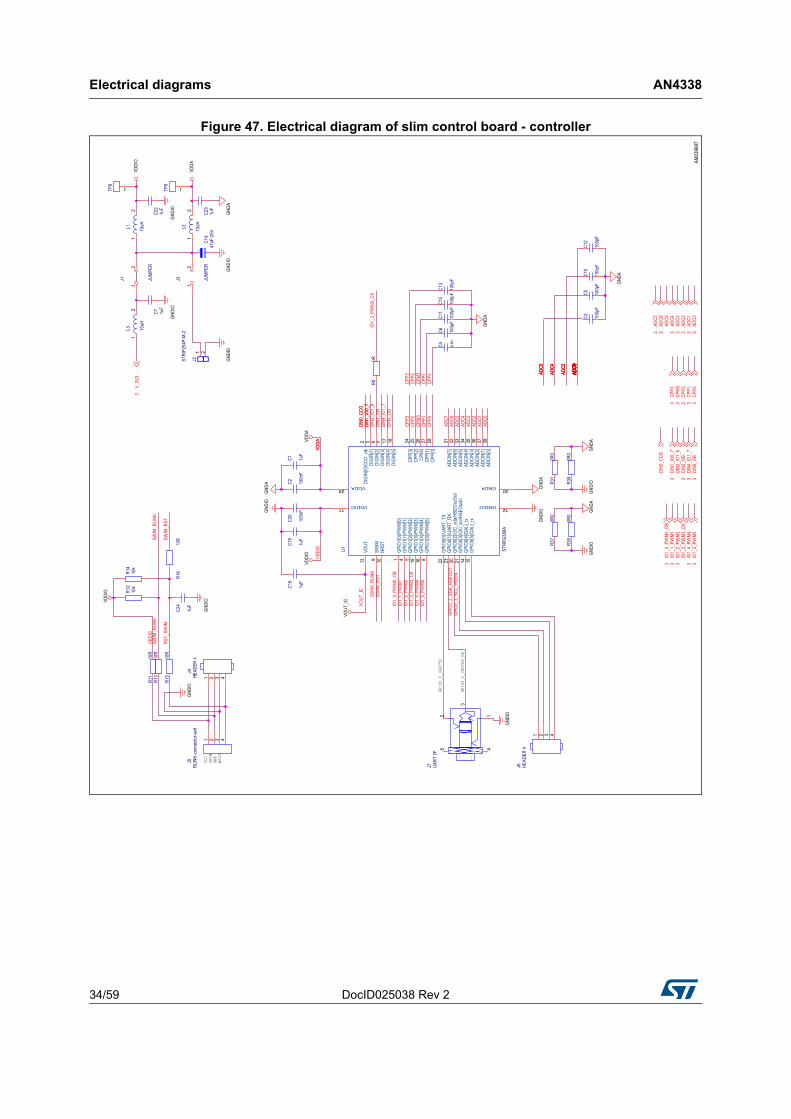
Figure 47. Electrical diagram of slim control board - controller
DocID025038 Rev 2 35/59
AN4338 Electrical diagrams
59
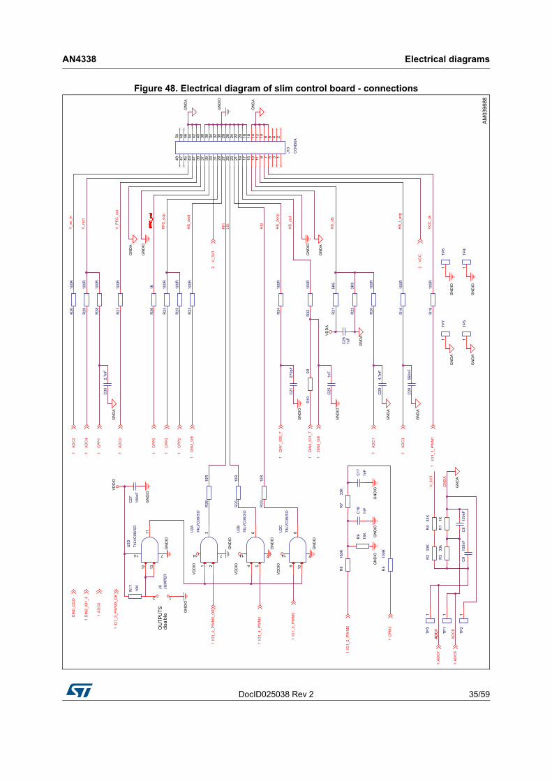
Figure 48. Electrical diagram of slim control board - connections

Electrical diagrams AN4338
36/59 DocID025038 Rev 2
It is worth highlighting that the aim of this evaluation board is to make the user acquainted the application and to provide a system for learning the use of the STNRG388A IC in power supply applications. As a consequence, this evaluation module is absolutely not optimized and contains many circuits that are disabled or are not actually used.

DocID025038 Rev 2 37/59
AN4338 Bill of materials
59
Appendix B Bill of materials
The detailed specifications of the PFC coil, resonant power transformer and auxiliary flyback transformer are available in the application note AN3329 of the EVL170W-FTV evaluation board. The bill of materials of the power board is shown in Table 5, while for the debug and slim control boards these are listed in Table 6 on page 48 and in Table 7 on page 54 respectively.
Table 5. Bill of materials EVLSTNRG-170W “power board”
Ref. Part Case Description Supplier
C1 2.2 nF Dia. 12 p.10 mm Y1 - safety cap. CD12-E2GA222MYGS TDK
C2 2.2 nF Dia. 12 p.10 mm Y1 - safety cap. CD12-E2GA222MYGS TDK
C3 270 pF 0805 16 V cercap. - general purpose - X7R - 10% KEMET
C4 100 F - 450 V Dia. 18 x 35 p.10 mm 450 V - aluminium elcap. - KXG series - 105 °CNIPPON
CHEMICON
C5 1 F - X2 11 x 26.5 p. 22.5 mm X2 - FLM CAP - B32923C3105K EPCOS
C6 1F - X2 11 x 26.5 p. 22.5 mm X2 - FLM CAP - B32923C3105K EPCOS
C7 470 nF-630 V 11 x 26.5 p. 22.5 mm 630 V - FLM CAP - B32613A6474K EPCOS
C8 470 nF-630 V 11 x 26.5 p. 22.5 mm 630 V - FLM CAP - B32613A6474K EPCOS
C9 100 F - 450 V Dia. 18 x 35 p.10 mm 450 V - aluminium elcap. - KXG series - 105 °CNIPPON
CHEMICON
C10 47 nF 1206 50 V cercap. - general purpose - X7R - 10% KEMET
C11 100 nF 1206 50 V cercap. - general purpose - X7R - 10% KEMET
C12 100 nF 1206 50 V cercap. - general purpose - X7R - 10% KEMET
C13 1000 F - 35 V Dia. 12 x 25 p. 5 mm Aluminium elcap. - YXF series - 105 °C RUBYCON
C14 1000 F - 35 V Dia. 12 x 25 p. 5 mm Aluminium elcap. - YXF series - 105 °C RUBYCON
C15 100 F - 50 V Dia. 8 x 11 p. 3.5 mm Aluminium elcap. - YXF series - 105 °C RUBYCON
C16 100 nF 0603 50 V cercap. - general purpose - X7R - 10% KEMET
C17 2.2 nF Dia. 12 p.10 mm Y1 - safety cap. CD12-E2GA222MYGS TDK
C18 4.7 nF 1206 500 V cercap. - 12067A221JAT2A - C0G - 5% AVX
C19 47 F - 50 VDia. 6.3 x 11 p. 2.5
mmAluminium elcap. - YXF series - 105 °C RUBYCON
C21 1000 F - 25 V Dia.12 x 20 p. 5 mm Aluminium elcap. - YXF series - 105 °C RUBYCON
C22 100 F - 50 V Dia. 8 x 11 p. 3.5 mm Aluminium elcap. - YXF series - 105 °C RUBYCON
C23 100 nF 0805 50 V cercap. - general purpose - X7R - 10% KEMET
C24 N. M. 0805
C25 100 nF 1206 50 V cercap. - general purpose - X7R - 10% KEMET
C26 100 nF 1206 50 V cercap. - general purpose - X7R - 10% KEMET
C27 220 pF 1206 500 V cercap. - 12067A221JAT2A - C0G - 5% AVX
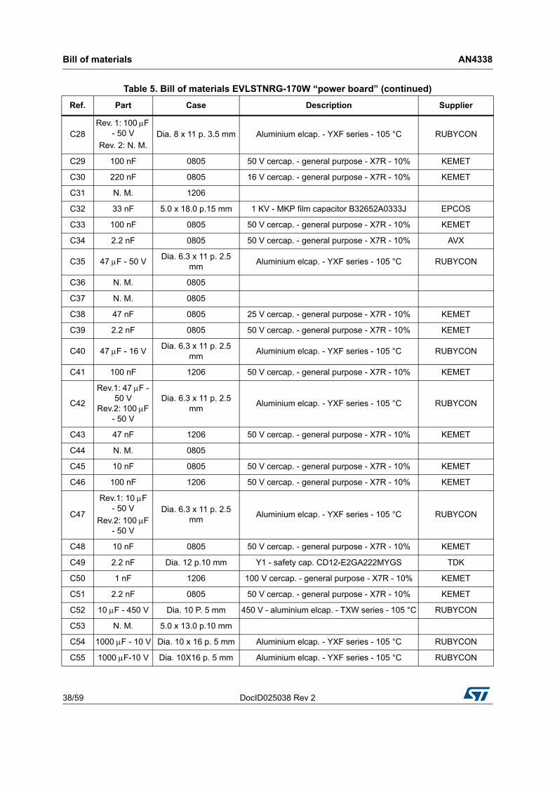
Bill of materials AN4338
38/59 DocID025038 Rev 2
C28Rev. 1: 100 F
- 50 V
Rev. 2: N. M.Dia. 8 x 11 p. 3.5 mm Aluminium elcap. - YXF series - 105 °C RUBYCON
C29 100 nF 0805 50 V cercap. - general purpose - X7R - 10% KEMET
C30 220 nF 0805 16 V cercap. - general purpose - X7R - 10% KEMET
C31 N. M. 1206
C32 33 nF 5.0 x 18.0 p.15 mm 1 KV - MKP film capacitor B32652A0333J EPCOS
C33 100 nF 0805 50 V cercap. - general purpose - X7R - 10% KEMET
C34 2.2 nF 0805 50 V cercap. - general purpose - X7R - 10% AVX
C35 47 F - 50 VDia. 6.3 x 11 p. 2.5
mmAluminium elcap. - YXF series - 105 °C RUBYCON
C36 N. M. 0805
C37 N. M. 0805
C38 47 nF 0805 25 V cercap. - general purpose - X7R - 10% KEMET
C39 2.2 nF 0805 50 V cercap. - general purpose - X7R - 10% KEMET
C40 47 F - 16 VDia. 6.3 x 11 p. 2.5
mmAluminium elcap. - YXF series - 105 °C RUBYCON
C41 100 nF 1206 50 V cercap. - general purpose - X7R - 10% KEMET
C42
Rev.1: 47 F - 50 V
Rev.2: 100 F - 50 V
Dia. 6.3 x 11 p. 2.5 mm
Aluminium elcap. - YXF series - 105 °C RUBYCON
C43 47 nF 1206 50 V cercap. - general purpose - X7R - 10% KEMET
C44 N. M. 0805
C45 10 nF 0805 50 V cercap. - general purpose - X7R - 10% KEMET
C46 100 nF 1206 50 V cercap. - general purpose - X7R - 10% KEMET
C47
Rev.1: 10 F - 50 V
Rev.2: 100 F - 50 V
Dia. 6.3 x 11 p. 2.5 mm
Aluminium elcap. - YXF series - 105 °C RUBYCON
C48 10 nF 0805 50 V cercap. - general purpose - X7R - 10% KEMET
C49 2.2 nF Dia. 12 p.10 mm Y1 - safety cap. CD12-E2GA222MYGS TDK
C50 1 nF 1206 100 V cercap. - general purpose - X7R - 10% KEMET
C51 2.2 nF 0805 50 V cercap. - general purpose - X7R - 10% KEMET
C52 10 F - 450 V Dia. 10 P. 5 mm 450 V - aluminium elcap. - TXW series - 105 °C RUBYCON
C53 N. M. 5.0 x 13.0 p.10 mm
C54 1000 F - 10 V Dia. 10 x 16 p. 5 mm Aluminium elcap. - YXF series - 105 °C RUBYCON
C55 1000 F-10 V Dia. 10X16 p. 5 mm Aluminium elcap. - YXF series - 105 °C RUBYCON
Table 5. Bill of materials EVLSTNRG-170W “power board” (continued)
Ref. Part Case Description Supplier
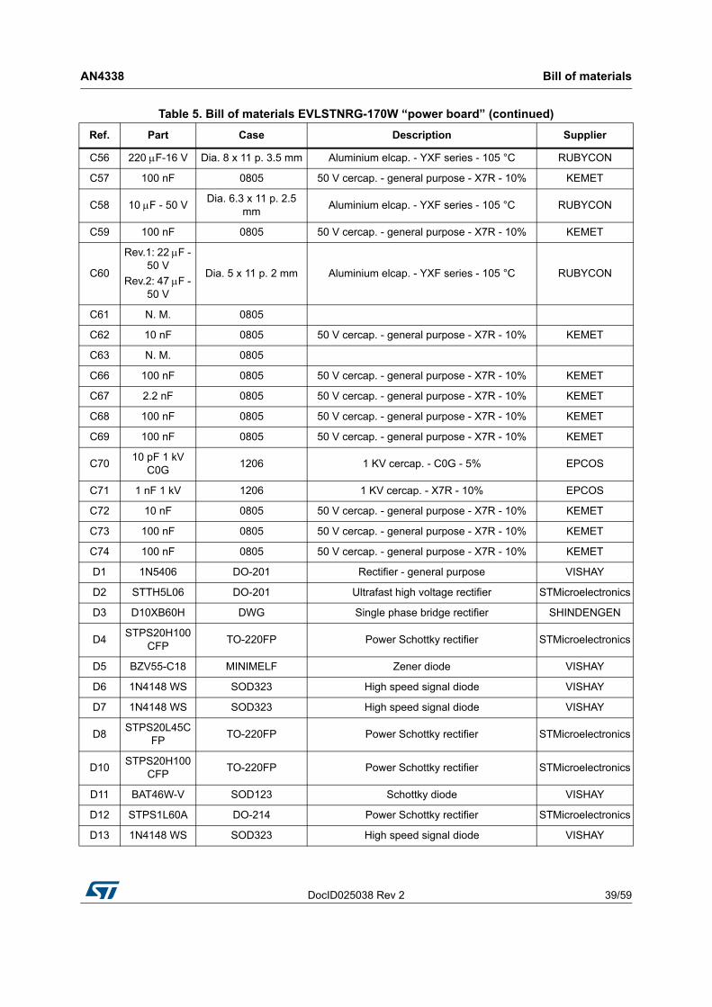
DocID025038 Rev 2 39/59
AN4338 Bill of materials
59
C56 220 F-16 V Dia. 8 x 11 p. 3.5 mm Aluminium elcap. - YXF series - 105 °C RUBYCON
C57 100 nF 0805 50 V cercap. - general purpose - X7R - 10% KEMET
C58 10 F - 50 VDia. 6.3 x 11 p. 2.5
mmAluminium elcap. - YXF series - 105 °C RUBYCON
C59 100 nF 0805 50 V cercap. - general purpose - X7R - 10% KEMET
C60
Rev.1: 22 F - 50 V
Rev.2: 47 F - 50 V
Dia. 5 x 11 p. 2 mm Aluminium elcap. - YXF series - 105 °C RUBYCON
C61 N. M. 0805
C62 10 nF 0805 50 V cercap. - general purpose - X7R - 10% KEMET
C63 N. M. 0805
C66 100 nF 0805 50 V cercap. - general purpose - X7R - 10% KEMET
C67 2.2 nF 0805 50 V cercap. - general purpose - X7R - 10% KEMET
C68 100 nF 0805 50 V cercap. - general purpose - X7R - 10% KEMET
C69 100 nF 0805 50 V cercap. - general purpose - X7R - 10% KEMET
C7010 pF 1 kV
C0G1206 1 KV cercap. - C0G - 5% EPCOS
C71 1 nF 1 kV 1206 1 KV cercap. - X7R - 10% EPCOS
C72 10 nF 0805 50 V cercap. - general purpose - X7R - 10% KEMET
C73 100 nF 0805 50 V cercap. - general purpose - X7R - 10% KEMET
C74 100 nF 0805 50 V cercap. - general purpose - X7R - 10% KEMET
D1 1N5406 DO-201 Rectifier - general purpose VISHAY
D2 STTH5L06 DO-201 Ultrafast high voltage rectifier STMicroelectronics
D3 D10XB60H DWG Single phase bridge rectifier SHINDENGEN
D4STPS20H100
CFPTO-220FP Power Schottky rectifier STMicroelectronics
D5 BZV55-C18 MINIMELF Zener diode VISHAY
D6 1N4148 WS SOD323 High speed signal diode VISHAY
D7 1N4148 WS SOD323 High speed signal diode VISHAY
D8STPS20L45C
FPTO-220FP Power Schottky rectifier STMicroelectronics
D10STPS20H100
CFPTO-220FP Power Schottky rectifier STMicroelectronics
D11 BAT46W-V SOD123 Schottky diode VISHAY
D12 STPS1L60A DO-214 Power Schottky rectifier STMicroelectronics
D13 1N4148 WS SOD323 High speed signal diode VISHAY
Table 5. Bill of materials EVLSTNRG-170W “power board” (continued)
Ref. Part Case Description Supplier

Bill of materials AN4338
40/59 DocID025038 Rev 2
D14 BZV55-C3 V3 MINIMELF Zener diode VISHAY
D15 BAT46W-V SOD123 Schottky diode VISHAY
D16 S1M DO-214 Rectifier - general purpose VISHAY
D17 S1M DO-214 Rectifier - general purpose VISHAY
D18 MMSZ4711-V SOD123 27 V Zener diode VISHAY
D19 MMSZ4702-V SOD123 15 V Zener diode VISHAY
D20 1N4148 WS SOD323 High speed signal diode VISHAY
D21 N. M. SOD123
D22 BAT46W-V SOD123 Schottky diode VISHAY
D23 P6KE250A DO-15 Transil™ STMicroelectronics
D24 BAV103 MINIMELF High speed signal diode VISHAY
D25STPS20L45C
FPTO-220FP Power Schottky rectifier STMicroelectronics
D26 STTH108A SMA HV ultrafast rectifier STMicroelectronics
D27 STTH102A SMA High efficiency ultrafast diode STMicroelectronics
D28 BAT46W-V SOD123 Schottky diode VISHAY
D29 N. M. MINIMELF
D30 STTH1R06A SMA Ultrafast high voltage rectifier STMicroelectronics
D31 BZV55-C13 MINIMELF Zener diode VISHAY
D32 BZV55-C3 V3 MINIMELF Zener diode VISHAY
D33 BAT46W-V SOD123 Schottky diode VISHAY
D34 STTH108A SMA HV ultrafast rectifier STMicroelectronics
D35 BAT46W-V SOD123 Schottky diode VISHAY
D36 BAT46W-V SOD123 Schottky diode VISHAY
F1 Fuse T4A 8.5 x 4 p. 5.08 mm Fuse 4 A - time LAG - 3921400 LITTLEFUSE
HOLE1 3 mm Threaded stand-off
HOLE2 3 mm Threaded stand-off
HOLE3 3 mm Threaded stand-off
HOLE4 3 mm Threaded stand-off
HOLE5 3 mm Threaded stand-off
HOLE6 3 mm Threaded stand-off
HS1 Heatsink DWG Heatsink for D4 and D10
HS2 Heatsink DWG Heatsink for Q4 and Q5
HS3 Heatsink DWG Heatsink for D3 and Q7
HS4 Heatsink DWG Heatsink for D8
Table 5. Bill of materials EVLSTNRG-170W “power board” (continued)
Ref. Part Case Description Supplier

DocID025038 Rev 2 41/59
AN4338 Bill of materials
59
HS5 Heatsink DWG Heatsink for D25
J1 MTA396-5Connector - p. 3.96 mm - 5 pins (2 removed) -
KKMOLEX
J2 CON50A Connector-FLAT P. 2.54 mm 25 x 2 rows 90 M
J3 280385-2 Connector - P. 2.54 mm - 8 x 2 rows - MODU-II AMP
J4 280384-2 Connector - P. 2.54 mm - 4 x 2 rows - MODU-II AMP
JP1 N. M. Wire jumper
JP2 Shorted Wire jumper
JPX1 Shorted Wire jumper
JPX2 Shorted Wire jumper
JPX3 Shorted Wire jumper
JPX4 Shorted Wire jumper
JPX5 Shorted Wire jumper
JPX6 Shorted Wire jumper
JPX7 Shorted Wire jumper
JPX8 Shorted Wire jumper
JPX9 Shorted Wire jumper
JPX10 Shorted Wire jumper
JPX11 Shorted Wire jumper
JPX12 Shorted Wire jumper
L1 1606.001 DWG 1606.0010 EMI filter 2 x 4 mH 3.3 A MAGNETICA
L2 2190.0001 26 x 13 mm 2190.0001 DM inductor 100 H 2.5 A MAGNETICA
L3 2086.0001 DWG 2086.0001 PFC inductor 240 H 2.65 A MAGNETICA
L4 1061.0014 Dia.12 p. 5 mm 1061.0041 inductor 2.9 H 11 A MAGNETICA
L5 1071.0083 Dia. 8 p. 5 mm 1071.0083 inductor 1 H 5 A MAGNETICA
L6 1071.0083 Dia. 8 p. 5 mm 1071.0083 inductor 1 H 5 A MAGNETICA
PCB1 PCB rev. 1.0.1 Dual layer - 2 OZ. - CEM-1
Q1 MMBT2222A SOT-23 NPN small signal BJT STMicroelectronics
Q2 MMBT2907A SOT-23 PNP small signal BJT STMicroelectronics
Q3 MMBT2222A SOT-23 NPN small signal BJT STMicroelectronics
Q4 STF14NM50N TO-220FP N-channel power MOSFET STMicroelectronics
Q5 STF14NM50N TO-220FP N-channel power MOSFET STMicroelectronics
Q6 MMBT2907A SOT-23 PNP small signal BJT STMicroelectronics
Q7 STF14NM50N TO-220FP N-channel power MOSFET STMicroelectronics
Q8 MMBT2222A SOT-23 NPN small signal BJT STMicroelectronics
Table 5. Bill of materials EVLSTNRG-170W “power board” (continued)
Ref. Part Case Description Supplier

Bill of materials AN4338
42/59 DocID025038 Rev 2
Q9 MMBT2907A SOT-23 PNP small signal BJT STMicroelectronics
Q10
Rev.1: BC847C
Rev. 2: PBSS4041NT
SOT-23 NPN small signal BJTRev.1: VISHAY
Rev.2: NXP
Q11 BC857C SOT-23 PNP small signal BJT VISHAY
Q12 BC847C SOT-23 NPN small signal BJT VISHAY
Q13 BC847C SOT-23 NPN small signal BJT VISHAY
R1 2.2 0805SMD standard film res. - 1/8 W - 5% - 250
ppm/°CVISHAY
R2NTC 2R5-
S237DWG NTC resistor P/N B57237S0259M000 EPCOS
R3 10 0805SMD standard film res. - 1/8 W - 5% - 250
ppm/°CVISHAY
R4 1 K 0805SMD standard film res. - 1/8 W - 5% - 250
ppm/°CVISHAY
R5 10 0805SMD standard film res. - 1/8 W - 5% - 250
ppm/°CVISHAY
R6 100 K 0805SMD standard film res. - 1/8 W - 5% - 250
ppm/°CVISHAY
R7 N. M. 0805
R8 2.7 K 0805SMD standard film res. - 1/8 W - 1% - 100
ppm/°CVISHAY
R9 56 0805SMD standard film res. - 1/8 W - 5% - 250
ppm/°CVISHAY
R10 3.3 K 1206SMD standard film res. - 1/4 W - 5% - 250
ppm/°CVISHAY
R11 2.2 0805SMD standard film res. - 1/8 W - 5% - 250
ppm/°CVISHAY
R12 3.9 K 1206SMD standard film res. - 1/4 W - 5% - 250
ppm/°CVISHAY
R13 N. M. 0805
R14 4.7 M 1206SMD standard film res. - 1/4 W - 1% - 100
ppm/°CVISHAY
R15 2.7 M 1206SMD standard film res. - 1/4 W - 1% - 100
ppm/°CVISHAY
R16 2.2 0805SMD standard film res. - 1/8 W - 5% - 250
ppm/°CVISHAY
R17 10 0805SMD standard film res. - 1/8 W - 5% - 250
ppm/°CVISHAY
Table 5. Bill of materials EVLSTNRG-170W “power board” (continued)
Ref. Part Case Description Supplier
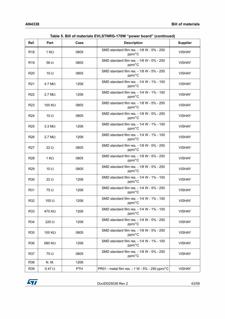
DocID025038 Rev 2 43/59
AN4338 Bill of materials
59
R18 1 K 0805SMD standard film res. - 1/8 W - 5% - 250
ppm/°CVISHAY
R19 56 0805SMD standard film res. - 1/8 W - 5% - 250
ppm/°CVISHAY
R20 10 0805SMD standard film res. - 1/8 W - 5% - 250
ppm/°CVISHAY
R21 4.7 M 1206SMD standard film res. - 1/4 W - 1% - 100
ppm/°CVISHAY
R22 2.7 M 1206SMD standard film res. - 1/4 W - 1% - 100
ppm/°CVISHAY
R23 100 K 0805SMD standard film res. - 1/8 W - 5% - 250
ppm/°CVISHAY
R24 10 0805SMD standard film res. - 1/8 W - 5% - 250
ppm/°CVISHAY
R25 3.3 M 1206SMD standard film res. - 1/4 W - 1% - 100
ppm/°CVISHAY
R26 2.7 M 1206SMD standard film res. - 1/4 W - 1% - 100
ppm/°CVISHAY
R27 22 0805SMD standard film res. - 1/8 W - 5% - 250
ppm/°CVISHAY
R28 1 K 0805SMD standard film res. - 1/8 W - 5% - 250
ppm/°CVISHAY
R29 10 0805SMD standard film res. - 1/8 W - 5% - 250
ppm/°CVISHAY
R30 22 1206SMD standard film res. - 1/4 W - 1% - 100
ppm/°CVISHAY
R31 75 1206SMD standard film res. - 1/4 W - 5% - 250
ppm/°CVISHAY
R32 100 1206SMD standard film res. - 1/4 W - 1% - 100
ppm/°CVISHAY
R33 470 K 1206SMD standard film res. - 1/4 W - 1% - 100
ppm/°CVISHAY
R34 220 1206SMD standard film res. - 1/4 W - 5% - 250
ppm/°CVISHAY
R35 100 K 0805SMD standard film res. - 1/8 W - 5% - 250
ppm/°CVISHAY
R36 680 K 1206SMD standard film res. - 1/4 W - 1% - 100
ppm/°CVISHAY
R37 75 0805SMD standard film res. - 1/8 W - 5% - 250
ppm/°CVISHAY
R38 N. M. 1206
R39 0.47 PTH PR01 - metal film res. - 1 W - 5% - 250 ppm/°C VISHAY
Table 5. Bill of materials EVLSTNRG-170W “power board” (continued)
Ref. Part Case Description Supplier

Bill of materials AN4338
44/59 DocID025038 Rev 2
R40 0.47 PTH PR01 - metal film res. - 1 W - 5% - 250 ppm/°C VISHAY
R41 0.47 PTH PR01 - metal film res. - 1 W - 5% - 250 ppm/°C VISHAY
R42 22 K 0805SMD standard film res. - 1/8 W - 1% - 100
ppm/°CVISHAY
R43 N. M. 0805
R44 N. M. 0805
R45 N. M. 0805
R46 1 K 0805SMD standard film res. - 1/8 W - 5% - 250
ppm/°CVISHAY
R47 5.6 K 0805SMD standard film res. - 1/8 W - 5% - 250
ppm/°CVISHAY
R48 180 K 0805SMD standard film res. - 1/8 W - 1% - 100
ppm/°CVISHAY
R49 51 0805SMD standard film res. - 1/8 W - 5% - 250
ppm/°CVISHAY
R50 N. M. 0805
R51 33 K 0805SMD standard film res. - 1/8 W - 5% - 250
ppm/°CVISHAY
R52 180 K 0805SMD standard film res. - 1/8 W - 5% - 250
ppm/°CVISHAY
R53 N. M. 0805
R54 N. M. 0805
R55 10 k 0805SMD standard film res. - 1/8 W - 1% - 100
ppm/°CVISHAY
R56 1.5 k 0805SMD standard film res. - 1/8 W - 5% - 250
ppm/°CVISHAY
R57 2.2 R 1206SMD standard film res. - 1/4 W - 5% - 250
ppm/°CVISHAY
R58 1 K 0805SMD standard film res. - 1/8 W - 5% - 250
ppm/°CVISHAY
R59 10 k 0805SMD standard film res. - 1/8 W - 5% - 250
ppm/°CVISHAY
R60 750 0805SMD standard film res. - 1/8 W - 5% - 250
ppm/°CVISHAY
R61 10 0805SMD standard film res. - 1/8 W - 5% - 250
ppm/°CVISHAY
R62 1 K 0805SMD standard film res. - 1/8 W - 5% - 250
ppm/°CVISHAY
R63 N. M. 0805
Table 5. Bill of materials EVLSTNRG-170W “power board” (continued)
Ref. Part Case Description Supplier

DocID025038 Rev 2 45/59
AN4338 Bill of materials
59
R64 1 K 0805SMD standard film res. - 1/8 W - 5% - 250
ppm/°CVISHAY
R65 4.7 M 1206SMD standard film res. - 1/4 W - 1% - 100
ppm/°CVISHAY
R66 N. M. 0805
R67 1 K 0805SMD standard film res. - 1/8 W - 5% - 250
ppm/°CVISHAY
R68 4.7 M 1206SMD standard film res. - 1/4 W - 1% - 100
ppm/°CVISHAY
R69 2.7 K 0805SMD standard film res. - 1/8 W - 5% - 250
ppm/°CVISHAY
R70 4.7 M 1206SMD standard film res. - 1/4 W - 1% - 100
ppm/°CVISHAY
R71 4.7 M 1206SMD standard film res. - 1/4 W - 1% - 100
ppm/°CVISHAY
R72 4.7 K 0805SMD standard film res. - 1/8 W - 5% - 250
ppm/°CVISHAY
R73 4.7 K 0805SMD standard film res. - 1/8 W - 5% - 250
ppm/°CVISHAY
R74 3.3 M 1206SMD standard film res. - 1/4 W - 1% - 100
ppm/°CVISHAY
R75 3.3 M 1206SMD standard film res. - 1/4 W - 1% - 100
ppm/°CVISHAY
R76 470 K 1206SMD standard film res. - 1/4 W - 1% - 100
ppm/°CVISHAY
R77 470 K 1206SMD standard film res. - 1/4 W - 1% - 100
ppm/°CVISHAY
R78 1 PTHNFR25H - axial fusible res. - 1/2 W - 5% - 100
ppm/°CVISHAY
R79 10 1206SMD standard film res. - 1/4 W - 5% - 250
ppm/°CVISHAY
R80 N. M. 1206
R81 33 K 0805SMD standard film res. - 1/8 W - 1% - 100
ppm/°CVISHAY
R82 N. M 0805
R83 N. M. PTH
R84 2.7 K 0805SMD standard film res. - 1/8 W - 5% - 250
ppm/°CVISHAY
R85 3.9 1206SMD standard film res. - 1/4 W - 5% - 250
ppm/°CVISHAY
Table 5. Bill of materials EVLSTNRG-170W “power board” (continued)
Ref. Part Case Description Supplier

Bill of materials AN4338
46/59 DocID025038 Rev 2
R86 1 K 0805SMD standard film res. - 1/8 W - 5% - 250
ppm/°CVISHAY
R87 12 K 0805SMD standard film res. - 1/8 W - 5% - 250
ppm/°CVISHAY
R88 390 K PTHAXIAL STD FILM RES - 1/8 W - 5% - 100
ppm/°CVISHAY
R89 N. M. 0805
R90 120 K 0805SMD standard film res. - 1/8 W - 1% - 100
ppm/°CVISHAY
R92 82 K 0805SMD standard film res. - 1/8 W - 1% - 100
ppm/°CVISHAY
R93 27 K 0805SMD standard film res. - 1/8 W - 5% - 250
ppm/°CVISHAY
R96 270 K 0805SMD standard film res. - 1/8 W - 5% - 250
ppm/°CVISHAY
R97 10 0805SMD standard film res. - 1/8 W - 5% - 250
ppm/°CVISHAY
R98 39 K 0805SMD standard film res. - 1/8 W - 1% - 100
ppm/°CVISHAY
R99 10 k 0805SMD standard film res. - 1/8 W - 5% - 250
ppm/°CVISHAY
R100 22 K 0805SMD standard film res. - 1/8 W - 5% - 250
ppm/°CVISHAY
R101 100 0805SMD standard film res. - 1/8 W - 5% - 250
ppm/°CVISHAY
R102 22 0805SMD standard film res. - 1/8 W - 5% - 250
ppm/°CVISHAY
R103 8.2 K 0805SMD standard film res. - 1/8 W - 5% - 250
ppm/°CVISHAY
R104 47 0805SMD standard film res. - 1/8 W - 5% - 250
ppm/°CVISHAY
R105 10 k 0805SMD standard film res. - 1/8 W - 5% - 250
ppm/°CVISHAY
R106 22 K 0805SMD standard film res. - 1/8 W - 5% - 250
ppm/°CVISHAY
R107 10 0805SMD standard film res. - 1/8 W - 5% - 250
ppm/°CVISHAY
R108 10 0805SMD standard film res. - 1/8 W - 5% - 250
ppm/°CVISHAY
R109 N. M. 0805
R110 10 k 1206SMD standard film res. - 1/4 W - 5% - 250
ppm/°CVISHAY
Table 5. Bill of materials EVLSTNRG-170W “power board” (continued)
Ref. Part Case Description Supplier
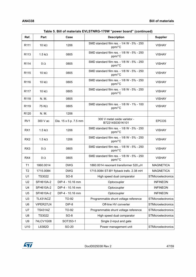
DocID025038 Rev 2 47/59
AN4338 Bill of materials
59
R111 10 k 1206SMD standard film res. - 1/4 W - 5% - 250
ppm/°CVISHAY
R113 1.5 k 0805SMD standard film res. - 1/8 W - 5% - 250
ppm/°CVISHAY
R114 0 0805SMD standard film res. - 1/8 W - 5% - 250
ppm/°CVISHAY
R115 10 k 0805SMD standard film res. - 1/8 W - 5% - 250
ppm/°CVISHAY
R116 10 k 0805SMD standard film res. - 1/8 W - 5% - 250
ppm/°CVISHAY
R117 10 k 0805SMD standard film res. - 1/8 W - 5% - 250
ppm/°CVISHAY
R118 N. M. 0805 VISHAY
R119 75 K 0805SMD standard film res. - 1/8 W - 1% - 100
ppm/°CVISHAY
R120 N. M. 1206
RV1 300 V ac Dia. 15 x 5 p. 7.5 mm300 V metal oxide varistor -
B72214S0301K101EPCOS
RX1 1.5 k 1206SMD standard film res. - 1/8 W - 5% - 250
ppm/°CVISHAY
RX2 1.5 k 1206SMD standard film res. - 1/8 W - 5% - 250
ppm/°CVISHAY
RX3 0 0805SMD standard film res. - 1/8 W - 5% - 250
ppm/°CVISHAY
RX4 0 0805SMD standard film res. - 1/8 W - 5% - 250
ppm/°CVISHAY
T1 1860.0014 DWG 1860.0014 resonant transformer 520 H MAGNETICA
T2 1715.0084 DWG 1715.0084 ST-BY flyback trafo. 2.38 mH MAGNETICA
U1 TS3022 SO-8 High speed dual comparator STMicroelectronics
U2 SFH610A-2 DIP-4 - 10.16 mm Optocoupler INFINEON
U4 SFH610A-2 DIP-4 - 10.16 mm Optocoupler INFINEON
U5 SFH610A-2 DIP-4 - 10.16 mm Optocoupler INFINEON
U3 TL431ACZ TO-92 Programmable shunt voltage reference STMicroelectronics
U6 VIPER27LN DIP-8 Off-line HV converter STMicroelectronics
U7 TS431AZ TO-92 Programmable shunt voltage reference STMicroelectronics
U8 TS3022 SO-8 High speed dual comparator STMicroelectronics
U9 74LCV1G08 SOT353-1 Single 2-input and gate
U10 L6382D SO-20 Power management unit STMicroelectronics
Table 5. Bill of materials EVLSTNRG-170W “power board” (continued)
Ref. Part Case Description Supplier
Bill of materials AN4338
48/59 DocID025038 Rev 2
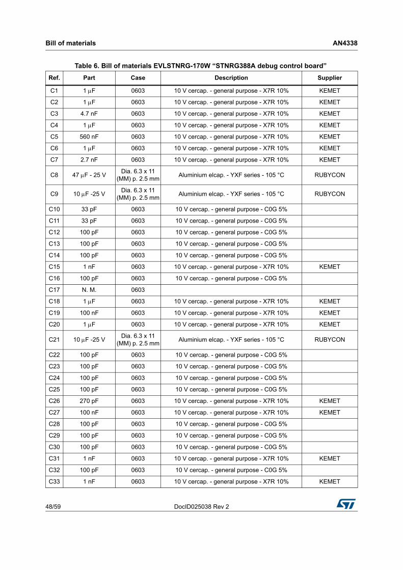
Table 6. Bill of materials EVLSTNRG-170W “STNRG388A debug control board”
Ref. Part Case Description Supplier
C1 1 F 0603 10 V cercap. - general purpose - X7R 10% KEMET
C2 1 F 0603 10 V cercap. - general purpose - X7R 10% KEMET
C3 4.7 nF 0603 10 V cercap. - general purpose - X7R 10% KEMET
C4 1 F 0603 10 V cercap. - general purpose - X7R 10% KEMET
C5 560 nF 0603 10 V cercap. - general purpose - X7R 10% KEMET
C6 1 F 0603 10 V cercap. - general purpose - X7R 10% KEMET
C7 2.7 nF 0603 10 V cercap. - general purpose - X7R 10% KEMET
C8 47 F - 25 VDia. 6.3 x 11
(MM) p. 2.5 mmAluminium elcap. - YXF series - 105 °C RUBYCON
C9 10 F -25 VDia. 6.3 x 11
(MM) p. 2.5 mmAluminium elcap. - YXF series - 105 °C RUBYCON
C10 33 pF 0603 10 V cercap. - general purpose - C0G 5%
C11 33 pF 0603 10 V cercap. - general purpose - C0G 5%
C12 100 pF 0603 10 V cercap. - general purpose - C0G 5%
C13 100 pF 0603 10 V cercap. - general purpose - C0G 5%
C14 100 pF 0603 10 V cercap. - general purpose - C0G 5%
C15 1 nF 0603 10 V cercap. - general purpose - X7R 10% KEMET
C16 100 pF 0603 10 V cercap. - general purpose - C0G 5%
C17 N. M. 0603
C18 1 F 0603 10 V cercap. - general purpose - X7R 10% KEMET
C19 100 nF 0603 10 V cercap. - general purpose - X7R 10% KEMET
C20 1 F 0603 10 V cercap. - general purpose - X7R 10% KEMET
C21 10 F -25 VDia. 6.3 x 11
(MM) p. 2.5 mmAluminium elcap. - YXF series - 105 °C RUBYCON
C22 100 pF 0603 10 V cercap. - general purpose - C0G 5%
C23 100 pF 0603 10 V cercap. - general purpose - C0G 5%
C24 100 pF 0603 10 V cercap. - general purpose - C0G 5%
C25 100 pF 0603 10 V cercap. - general purpose - C0G 5%
C26 270 pF 0603 10 V cercap. - general purpose - X7R 10% KEMET
C27 100 nF 0603 10 V cercap. - general purpose - X7R 10% KEMET
C28 100 pF 0603 10 V cercap. - general purpose - C0G 5%
C29 100 pF 0603 10 V cercap. - general purpose - C0G 5%
C30 100 pF 0603 10 V cercap. - general purpose - C0G 5%
C31 1 nF 0603 10 V cercap. - general purpose - X7R 10% KEMET
C32 100 pF 0603 10 V cercap. - general purpose - C0G 5%
C33 1 nF 0603 10 V cercap. - general purpose - X7R 10% KEMET
DocID025038 Rev 2 49/59
AN4338 Bill of materials
59
C34 1 F 0603 25 V cercap. - general purpose - X7R 10% KEMET
C35 100 nF 0603 10 V cercap. - general purpose - X7R 10% KEMET
C36 100 nF 0603 10 V cercap. - general purpose - X7R 10% KEMET
C37 1 F 0603 10 V cercap. - general purpose - X7R 10% KEMET
C38 100 nF 0603 10 V cercap. - general purpose - X7R 10% KEMET
C39 1 F 0603 10 V cercap. - general purpose - X7R 10% KEMET
C40 100 nF 0603 10 V cercap. - general purpose - X7R 10% KEMET
D1 OVS-0608 0603 LED red
D2 OVS-0608 0603 LED red
D3 OVS-0608 0603 LED red
D4 OVS-0608 0603 LED red
D5 OVS-0608 0603 LED red
D6 OVS-0608 0603 LED red
D7 OVS-0608 0603 LED red
D8 OVS-0608 0603 LED red
J1 Jumper Strip P 254 mm M 2
J2 Conn. V_3 V3_ext MORSQC508-ADIMPEX-MK159002
J3 Jumper Strip P 254 mm M 2
J4 Conn. PCB 5 Strip P 254 mm M 5
J5 Conn. PCB 5 Strip P 254 mm M 5
J6 Conn. PCB 8 Strip P 254 mm M 8
J7 CON50A CON-FLAT_CABLE P 254 mm 25 x 2 90 F
J8 Conn. PCB 8 Strip P 254 mm M 8
J9 Conn. PCB 8 Strip P 254 mm M 8
J10 Jumper Strip P 254 mm M 2
J11 Jumper Strip P 254 mm M 2
J12 Conn. VCC_ext MORSQC508-ADIMPEX-MK159002
J13 Strip254P-M-2 Strip P 254 mm M 2
J14 Conn. PCB 8 Strip P 254 mm M 8
J15 Conn. PCB 8 Strip P 254 mm M 8
J16 UART I/F 3.5 mm JACK SC-35RASMT4BHNTRX
J17 Jumper Strip P 254 mm M 2
J18 Jumper Strip P 254 mm M 2
J19 Jumper Strip P 254 mm M 2
J20 Jumper Strip P 254 mm M 2
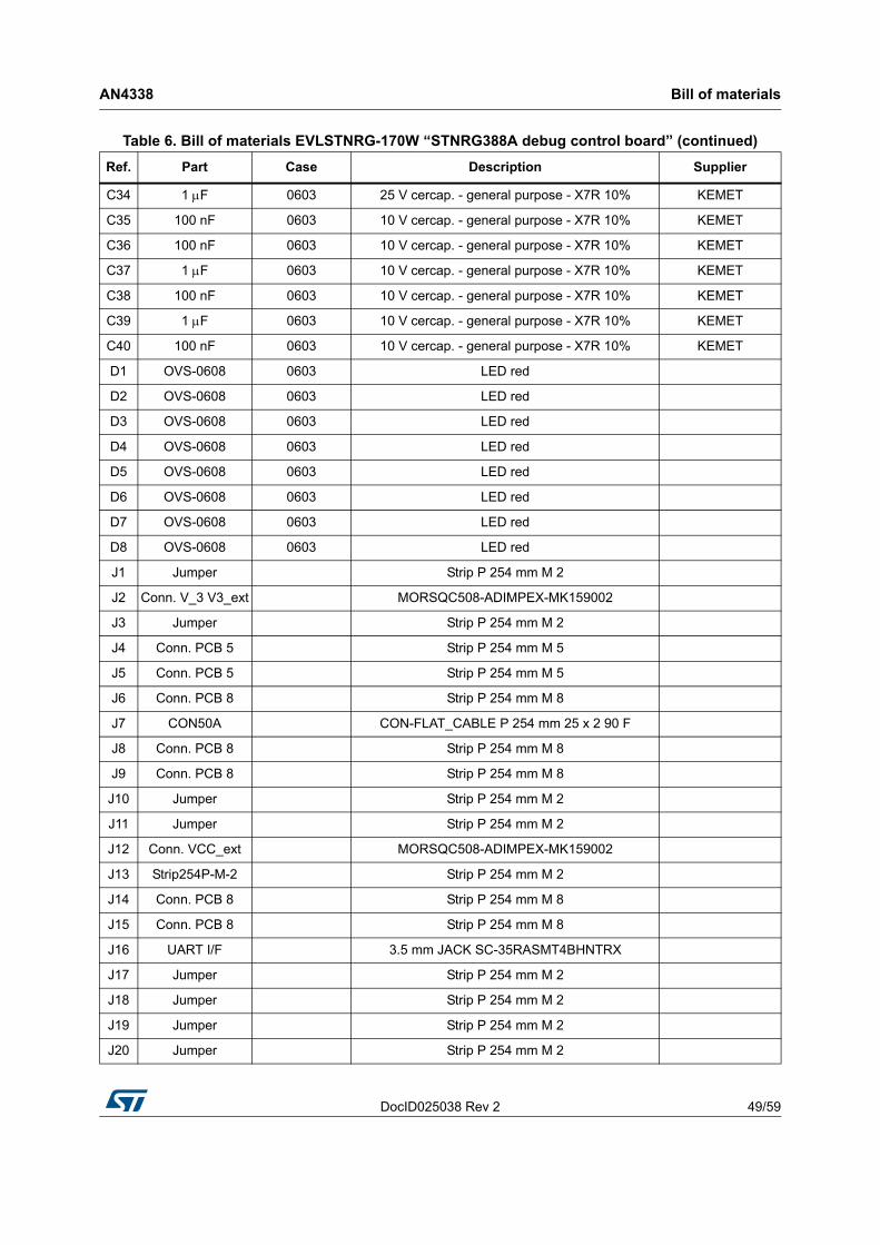
Table 6. Bill of materials EVLSTNRG-170W “STNRG388A debug control board” (continued)
Ref. Part Case Description Supplier

Bill of materials AN4338
50/59 DocID025038 Rev 2
J21 Jumper Strip P 254 mm M 4
J22 Jumper Strip P 254 mm M 4
J23 Header 4 Strip P 254 mm M 4
J24 Jumper Strip P 254 mm M 2
J25 Jumper Strip P 254 mm M 2
J27RLink-connector-
vert.ERNI_284697 ERNI
L1 10 H 1206 SMD inductor
L2 10 H 1206 SMD inductor
L3 10 H 1206 SMD inductor
L4 10 H 1206 SMD inductor
R1 3.9 K 0603 SMD standard film res. - 1/8 W - 1% - 100 ppm/°C VISHAY
R2 5.6 K 0603 SMD standard film res. - 1/8 W - 1% - 100 ppm/°C VISHAY
R3 100 0603 SMD standard film res. - 1/8 W - 1% - 100 ppm/°C VISHAY
R4 100 0603 SMD standard film res. - 1/8 W - 1% - 100 ppm/°C VISHAY
R5 100 0603 SMD standard film res. - 1/8 W - 1% - 100 ppm/°C VISHAY
R6 100 0603 SMD standard film res. - 1/8 W - 1% - 100 ppm/°C VISHAY
R7 100 0603 SMD standard film res. - 1/8 W - 1% - 100 ppm/°C VISHAY
R8 3.3 k 0603 SMD standard film res. - 1/8 W - 1% - 100 ppm/°C VISHAY
R9 1 K 0603 SMD standard film res. - 1/8 W - 1% - 100 ppm/°C VISHAY
R10 100 0603 SMD standard film res. - 1/8 W - 1% - 100 ppm/°C VISHAY
R11 100 0603 SMD standard film res. - 1/8 W - 1% - 100 ppm/°C VISHAY
R12 100 0603 SMD standard film res. - 1/8 W - 1% - 100 ppm/°C VISHAY
R13 0 0805 SMD standard film res. - 1/8 W - 1% - 100 ppm/°C VISHAY
R14 0 0805 SMD standard film res. - 1/8 W - 1% - 100 ppm/°C VISHAY
R15 0 0805 SMD standard film res. - 1/8 W - 1% - 100 ppm/°C VISHAY
R16 0 0805 SMD standard film res. - 1/8 W - 1% - 100 ppm/°C VISHAY
R17 0 0805 SMD standard film res. - 1/8 W - 1% - 100 ppm/°C VISHAY
R18 100 0603 SMD standard film res. - 1/8 W - 1% - 100 ppm/°C VISHAY
R19 100 0603 SMD standard film res. - 1/8 W - 1% - 100 ppm/°C VISHAY
R20 N. M. 0603
R21 N. M. 0603
R22 100 0603 SMD standard film res. - 1/8 W - 1% - 100 ppm/°C VISHAY
R23 100 0603 SMD standard film res. - 1/8 W - 1% - 100 ppm/°C VISHAY
R24 0 0603 SMD standard film res. - 1/8 W - 1% - 100 ppm/°C VISHAY
Table 6. Bill of materials EVLSTNRG-170W “STNRG388A debug control board” (continued)
Ref. Part Case Description Supplier
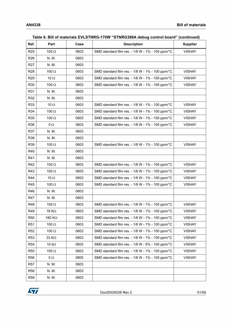
DocID025038 Rev 2 51/59
AN4338 Bill of materials
59
R25 100 0603 SMD standard film res. - 1/8 W - 1% - 100 ppm/°C VISHAY
R26 N. M. 0603
R27 N. M. 0603
R28 100 0603 SMD standard film res. - 1/8 W - 1% - 100 ppm/°C VISHAY
R29 10 0603 SMD standard film res. - 1/8 W - 1% - 100 ppm/°C VISHAY
R30 100 0603 SMD standard film res. - 1/8 W - 1% - 100 ppm/°C VISHAY
R31 N. M. 0603
R32 N. M. 0603
R33 10 0603 SMD standard film res. - 1/8 W - 1% - 100 ppm/°C VISHAY
R34 100 0603 SMD standard film res. - 1/8 W - 1% - 100 ppm/°C VISHAY
R35 100 0603 SMD standard film res. - 1/8 W - 1% - 100 ppm/°C VISHAY
R36 0 0603 SMD standard film res. - 1/8 W - 1% - 100 ppm/°C VISHAY
R37 N. M. 0603
R38 N. M. 0603
R39 100 0603 SMD standard film res. - 1/8 W - 1% - 100 ppm/°C VISHAY
R40 N. M. 0603
R41 N. M. 0603
R42 100 0603 SMD standard film res. - 1/8 W - 1% - 100 ppm/°C VISHAY
R43 100 0603 SMD standard film res. - 1/8 W - 1% - 100 ppm/°C VISHAY
R44 10 0603 SMD standard film res. - 1/8 W - 1% - 100 ppm/°C VISHAY
R45 100 0603 SMD standard film res. - 1/8 W - 1% - 100 ppm/°C VISHAY
R46 N. M. 0603
R47 N. M. 0603
R48 100 0603 SMD standard film res. - 1/8 W - 1% - 100 ppm/°C VISHAY
R49 18 K 0603 SMD standard film res. - 1/8 W - 1% - 100 ppm/°C VISHAY
R50 180 K 0603 SMD standard film res. - 1/8 W - 1% - 100 ppm/°C VISHAY
R51 100 0603 SMD standard film res. - 1/8 W - 1% - 100 ppm/°C VISHAY
R52 100 0603 SMD standard film res. - 1/8 W - 1% - 100 ppm/°C VISHAY
R53 33 K 0603 SMD standard film res. - 1/8 W - 1% - 100 ppm/°C VISHAY
R54 10 k 0603 SMD standard film res. - 1/8 W - 5% - 100 ppm/°C VISHAY
R55 100 0603 SMD standard film res. - 1/8 W - 1% - 100 ppm/°C VISHAY
R56 0 0805 SMD standard film res. - 1/8 W - 1% - 100 ppm/°C VISHAY
R57 N. M. 0603
R58 N. M. 0603
R59 N. M. 0603
Table 6. Bill of materials EVLSTNRG-170W “STNRG388A debug control board” (continued)
Ref. Part Case Description Supplier
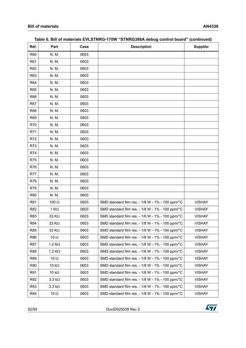
Bill of materials AN4338
52/59 DocID025038 Rev 2
R60 N. M. 0603
R61 N. M. 0603
R62 N. M. 0603
R63 N. M. 0603
R64 N. M. 0603
R65 N. M. 0603
R66 N. M. 0603
R67 N. M. 0603
R68 N. M. 0603
R69 N. M. 0603
R70 N. M. 0603
R71 N. M. 0603
R72 N. M. 0603
R73 N. M. 0603
R74 N. M. 0603
R75 N. M. 0603
R76 N. M. 0603
R77 N. M. 0603
R78 N. M. 0603
R79 N. M. 0603
R80 N. M. 0603
R81 100 0603 SMD standard film res. - 1/8 W - 1% - 100 ppm/°C VISHAY
R82 1 K 0603 SMD standard film res. - 1/8 W - 1% - 100 ppm/°C VISHAY
R83 33 K 0603 SMD standard film res. - 1/8 W - 1% - 100 ppm/°C VISHAY
R84 33 K 0603 SMD standard film res. - 1/8 W - 1% - 100 ppm/°C VISHAY
R85 33 K 0603 SMD standard film res. - 1/8 W - 1% - 100 ppm/°C VISHAY
R86 10 0603 SMD standard film res. - 1/8 W - 1% - 100 ppm/°C VISHAY
R87 1.2 K 0603 SMD standard film res. - 1/8 W - 1% - 100 ppm/°C VISHAY
R88 1.2 K 0603 SMD standard film res. - 1/8 W - 1% - 100 ppm/°C VISHAY
R89 10 0603 SMD standard film res. - 1/8 W - 1% - 100 ppm/°C VISHAY
R90 10 k 0603 SMD standard film res. - 1/8 W - 1% - 100 ppm/°C VISHAY
R91 10 k 0603 SMD standard film res. - 1/8 W - 1% - 100 ppm/°C VISHAY
R92 3.3 k 0603 SMD standard film res. - 1/8 W - 1% - 100 ppm/°C VISHAY
R93 3.3 k 0603 SMD standard film res. - 1/8 W - 1% - 100 ppm/°C VISHAY
R94 10 0603 SMD standard film res. - 1/8 W - 1% - 100 ppm/°C VISHAY
Table 6. Bill of materials EVLSTNRG-170W “STNRG388A debug control board” (continued)
Ref. Part Case Description Supplier
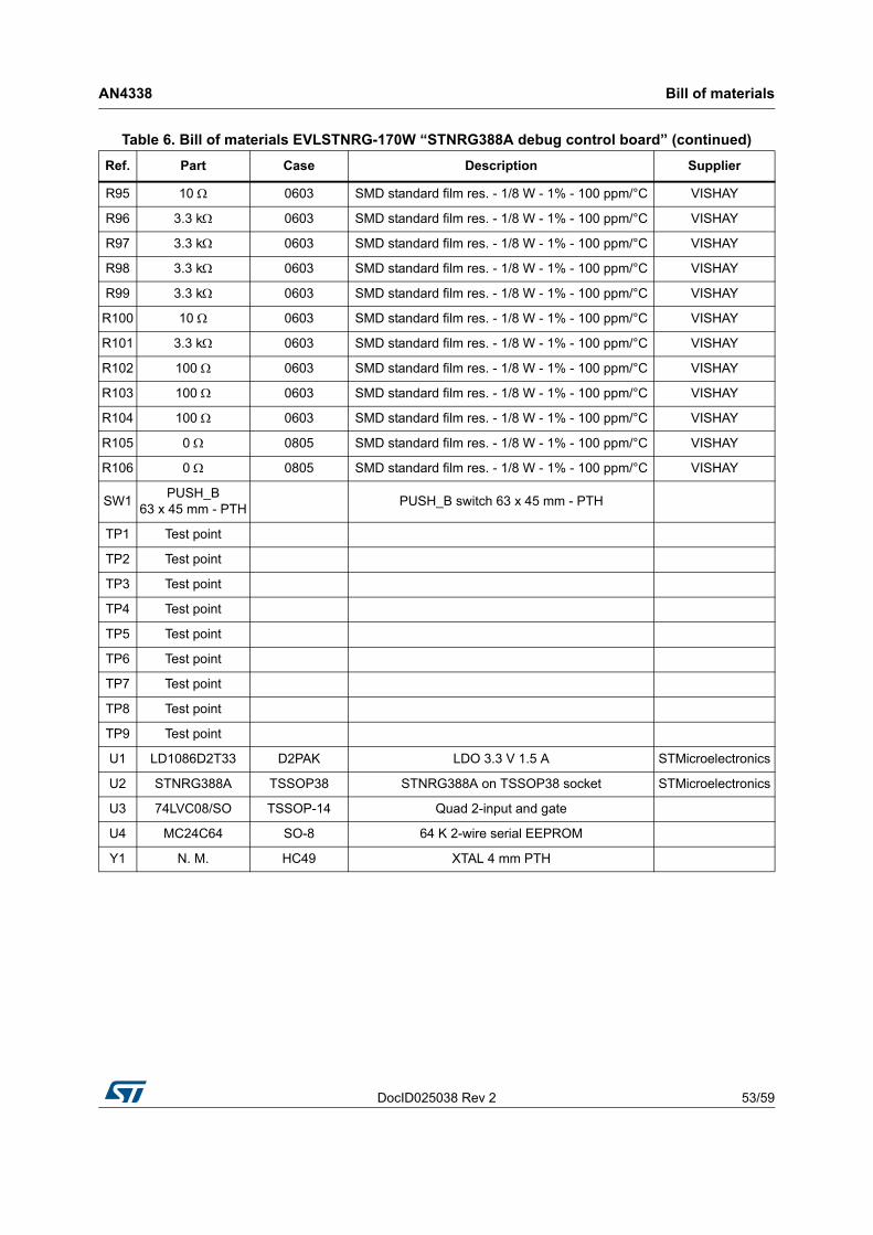
DocID025038 Rev 2 53/59
AN4338 Bill of materials
59
R95 10 0603 SMD standard film res. - 1/8 W - 1% - 100 ppm/°C VISHAY
R96 3.3 k 0603 SMD standard film res. - 1/8 W - 1% - 100 ppm/°C VISHAY
R97 3.3 k 0603 SMD standard film res. - 1/8 W - 1% - 100 ppm/°C VISHAY
R98 3.3 k 0603 SMD standard film res. - 1/8 W - 1% - 100 ppm/°C VISHAY
R99 3.3 k 0603 SMD standard film res. - 1/8 W - 1% - 100 ppm/°C VISHAY
R100 10 0603 SMD standard film res. - 1/8 W - 1% - 100 ppm/°C VISHAY
R101 3.3 k 0603 SMD standard film res. - 1/8 W - 1% - 100 ppm/°C VISHAY
R102 100 0603 SMD standard film res. - 1/8 W - 1% - 100 ppm/°C VISHAY
R103 100 0603 SMD standard film res. - 1/8 W - 1% - 100 ppm/°C VISHAY
R104 100 0603 SMD standard film res. - 1/8 W - 1% - 100 ppm/°C VISHAY
R105 0 0805 SMD standard film res. - 1/8 W - 1% - 100 ppm/°C VISHAY
R106 0 0805 SMD standard film res. - 1/8 W - 1% - 100 ppm/°C VISHAY
SW1PUSH_B
63 x 45 mm - PTHPUSH_B switch 63 x 45 mm - PTH
TP1 Test point
TP2 Test point
TP3 Test point
TP4 Test point
TP5 Test point
TP6 Test point
TP7 Test point
TP8 Test point
TP9 Test point
U1 LD1086D2T33 D2PAK LDO 3.3 V 1.5 A STMicroelectronics
U2 STNRG388A TSSOP38 STNRG388A on TSSOP38 socket STMicroelectronics
U3 74LVC08/SO TSSOP-14 Quad 2-input and gate
U4 MC24C64 SO-8 64 K 2-wire serial EEPROM
Y1 N. M. HC49 XTAL 4 mm PTH
Table 6. Bill of materials EVLSTNRG-170W “STNRG388A debug control board” (continued)
Ref. Part Case Description Supplier
Bill of materials AN4338
54/59 DocID025038 Rev 2
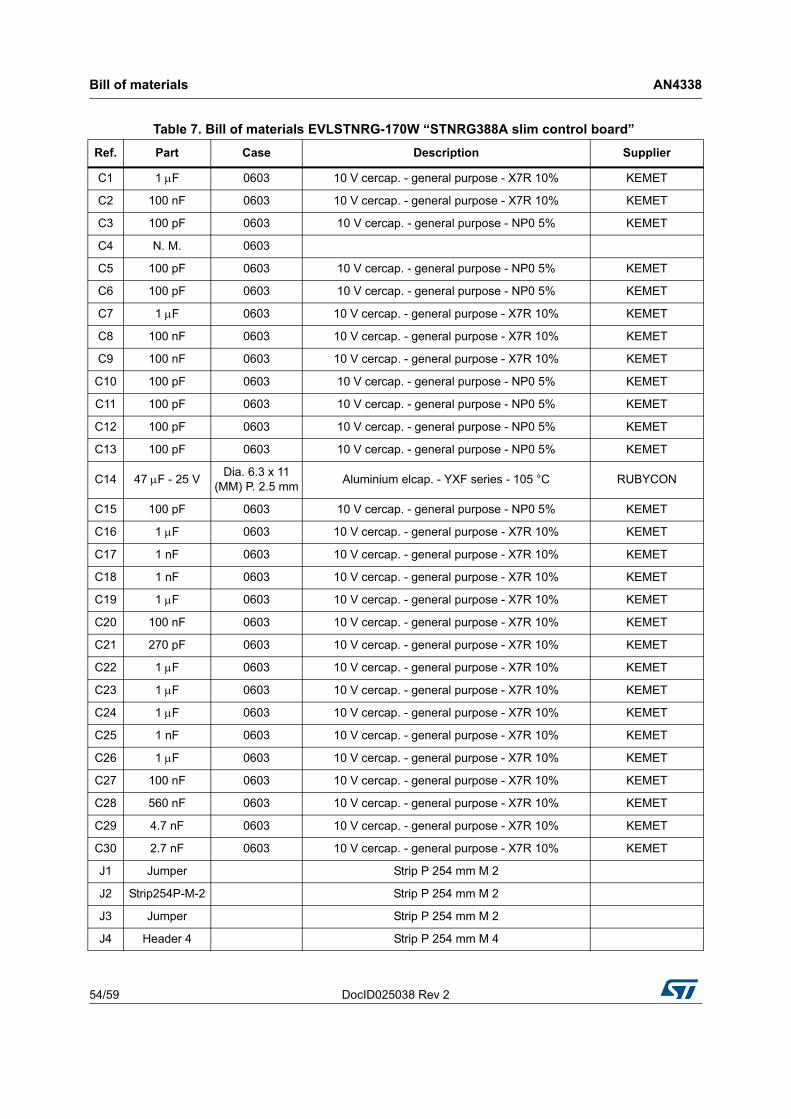
Table 7. Bill of materials EVLSTNRG-170W “STNRG388A slim control board”
Ref. Part Case Description Supplier
C1 1 F 0603 10 V cercap. - general purpose - X7R 10% KEMET
C2 100 nF 0603 10 V cercap. - general purpose - X7R 10% KEMET
C3 100 pF 0603 10 V cercap. - general purpose - NP0 5% KEMET
C4 N. M. 0603
C5 100 pF 0603 10 V cercap. - general purpose - NP0 5% KEMET
C6 100 pF 0603 10 V cercap. - general purpose - NP0 5% KEMET
C7 1 F 0603 10 V cercap. - general purpose - X7R 10% KEMET
C8 100 nF 0603 10 V cercap. - general purpose - X7R 10% KEMET
C9 100 nF 0603 10 V cercap. - general purpose - X7R 10% KEMET
C10 100 pF 0603 10 V cercap. - general purpose - NP0 5% KEMET
C11 100 pF 0603 10 V cercap. - general purpose - NP0 5% KEMET
C12 100 pF 0603 10 V cercap. - general purpose - NP0 5% KEMET
C13 100 pF 0603 10 V cercap. - general purpose - NP0 5% KEMET
C14 47 F - 25 VDia. 6.3 x 11
(MM) P. 2.5 mmAluminium elcap. - YXF series - 105 °C RUBYCON
C15 100 pF 0603 10 V cercap. - general purpose - NP0 5% KEMET
C16 1 F 0603 10 V cercap. - general purpose - X7R 10% KEMET
C17 1 nF 0603 10 V cercap. - general purpose - X7R 10% KEMET
C18 1 nF 0603 10 V cercap. - general purpose - X7R 10% KEMET
C19 1 F 0603 10 V cercap. - general purpose - X7R 10% KEMET
C20 100 nF 0603 10 V cercap. - general purpose - X7R 10% KEMET
C21 270 pF 0603 10 V cercap. - general purpose - X7R 10% KEMET
C22 1 F 0603 10 V cercap. - general purpose - X7R 10% KEMET
C23 1 F 0603 10 V cercap. - general purpose - X7R 10% KEMET
C24 1 F 0603 10 V cercap. - general purpose - X7R 10% KEMET
C25 1 nF 0603 10 V cercap. - general purpose - X7R 10% KEMET
C26 1 F 0603 10 V cercap. - general purpose - X7R 10% KEMET
C27 100 nF 0603 10 V cercap. - general purpose - X7R 10% KEMET
C28 560 nF 0603 10 V cercap. - general purpose - X7R 10% KEMET
C29 4.7 nF 0603 10 V cercap. - general purpose - X7R 10% KEMET
C30 2.7 nF 0603 10 V cercap. - general purpose - X7R 10% KEMET
J1 Jumper Strip P 254 mm M 2
J2 Strip254P-M-2 Strip P 254 mm M 2
J3 Jumper Strip P 254 mm M 2
J4 Header 4 Strip P 254 mm M 4
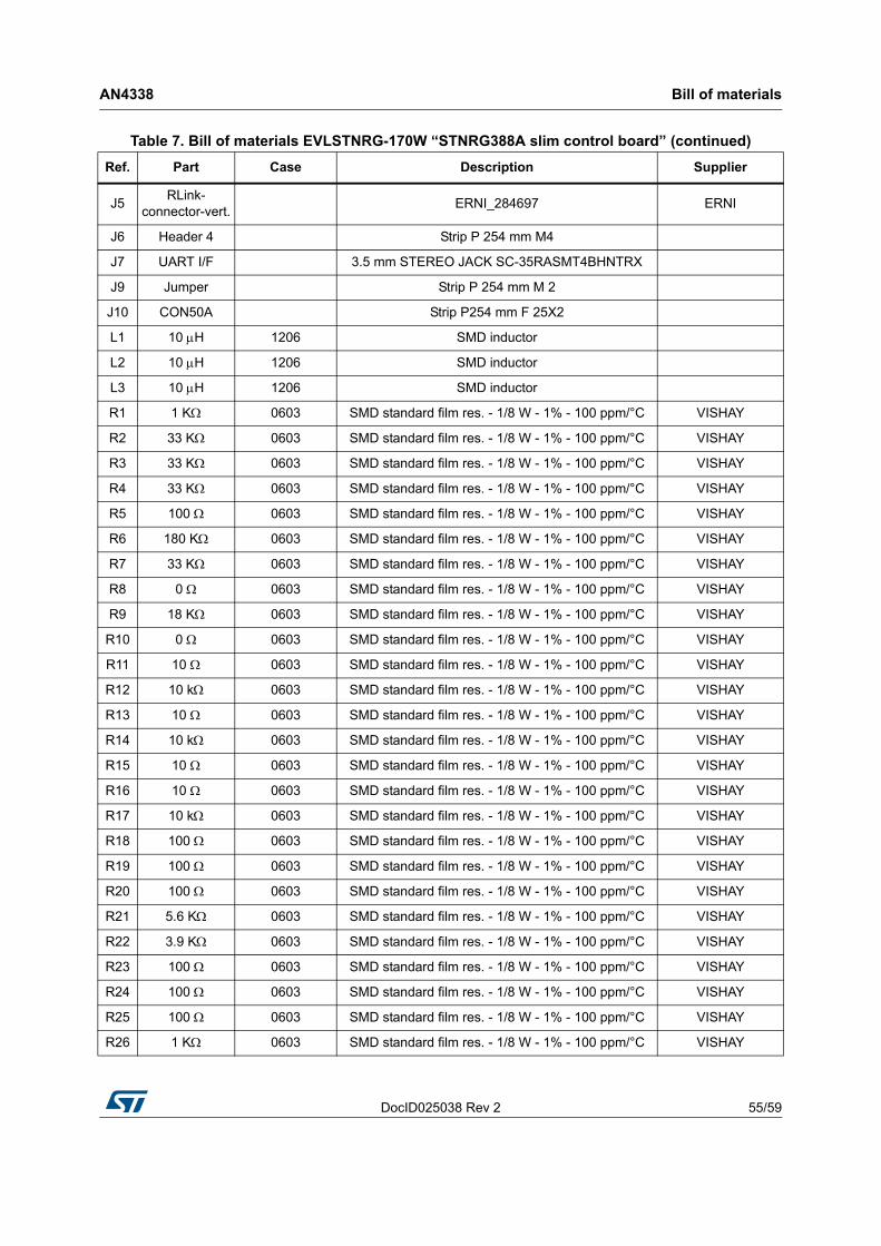
DocID025038 Rev 2 55/59
AN4338 Bill of materials
59
J5RLink-
connector-vert.ERNI_284697 ERNI
J6 Header 4 Strip P 254 mm M4
J7 UART I/F 3.5 mm STEREO JACK SC-35RASMT4BHNTRX
J9 Jumper Strip P 254 mm M 2
J10 CON50A Strip P254 mm F 25X2
L1 10 H 1206 SMD inductor
L2 10 H 1206 SMD inductor
L3 10 H 1206 SMD inductor
R1 1 K 0603 SMD standard film res. - 1/8 W - 1% - 100 ppm/°C VISHAY
R2 33 K 0603 SMD standard film res. - 1/8 W - 1% - 100 ppm/°C VISHAY
R3 33 K 0603 SMD standard film res. - 1/8 W - 1% - 100 ppm/°C VISHAY
R4 33 K 0603 SMD standard film res. - 1/8 W - 1% - 100 ppm/°C VISHAY
R5 100 0603 SMD standard film res. - 1/8 W - 1% - 100 ppm/°C VISHAY
R6 180 K 0603 SMD standard film res. - 1/8 W - 1% - 100 ppm/°C VISHAY
R7 33 K 0603 SMD standard film res. - 1/8 W - 1% - 100 ppm/°C VISHAY
R8 0 0603 SMD standard film res. - 1/8 W - 1% - 100 ppm/°C VISHAY
R9 18 K 0603 SMD standard film res. - 1/8 W - 1% - 100 ppm/°C VISHAY
R10 0 0603 SMD standard film res. - 1/8 W - 1% - 100 ppm/°C VISHAY
R11 10 0603 SMD standard film res. - 1/8 W - 1% - 100 ppm/°C VISHAY
R12 10 k 0603 SMD standard film res. - 1/8 W - 1% - 100 ppm/°C VISHAY
R13 10 0603 SMD standard film res. - 1/8 W - 1% - 100 ppm/°C VISHAY
R14 10 k 0603 SMD standard film res. - 1/8 W - 1% - 100 ppm/°C VISHAY
R15 10 0603 SMD standard film res. - 1/8 W - 1% - 100 ppm/°C VISHAY
R16 10 0603 SMD standard film res. - 1/8 W - 1% - 100 ppm/°C VISHAY
R17 10 k 0603 SMD standard film res. - 1/8 W - 1% - 100 ppm/°C VISHAY
R18 100 0603 SMD standard film res. - 1/8 W - 1% - 100 ppm/°C VISHAY
R19 100 0603 SMD standard film res. - 1/8 W - 1% - 100 ppm/°C VISHAY
R20 100 0603 SMD standard film res. - 1/8 W - 1% - 100 ppm/°C VISHAY
R21 5.6 K 0603 SMD standard film res. - 1/8 W - 1% - 100 ppm/°C VISHAY
R22 3.9 K 0603 SMD standard film res. - 1/8 W - 1% - 100 ppm/°C VISHAY
R23 100 0603 SMD standard film res. - 1/8 W - 1% - 100 ppm/°C VISHAY
R24 100 0603 SMD standard film res. - 1/8 W - 1% - 100 ppm/°C VISHAY
R25 100 0603 SMD standard film res. - 1/8 W - 1% - 100 ppm/°C VISHAY
R26 1 K 0603 SMD standard film res. - 1/8 W - 1% - 100 ppm/°C VISHAY
Table 7. Bill of materials EVLSTNRG-170W “STNRG388A slim control board” (continued)
Ref. Part Case Description Supplier
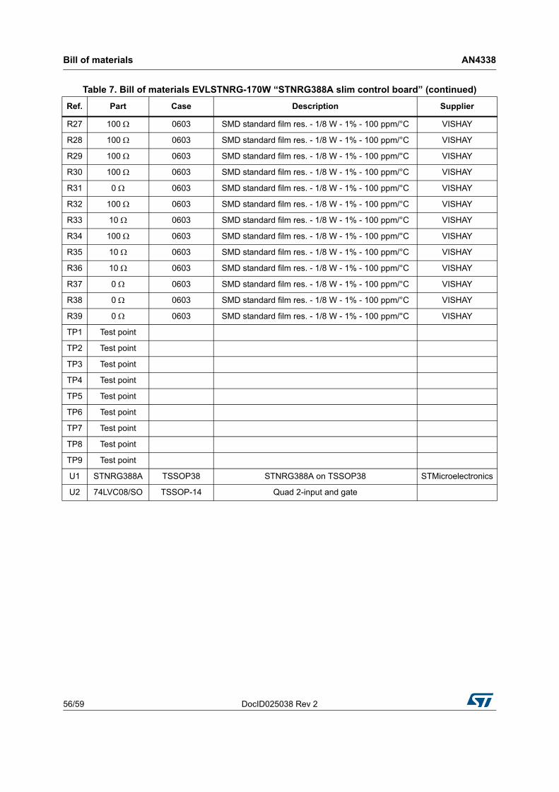
Bill of materials AN4338
56/59 DocID025038 Rev 2
R27 100 0603 SMD standard film res. - 1/8 W - 1% - 100 ppm/°C VISHAY
R28 100 0603 SMD standard film res. - 1/8 W - 1% - 100 ppm/°C VISHAY
R29 100 0603 SMD standard film res. - 1/8 W - 1% - 100 ppm/°C VISHAY
R30 100 0603 SMD standard film res. - 1/8 W - 1% - 100 ppm/°C VISHAY
R31 0 0603 SMD standard film res. - 1/8 W - 1% - 100 ppm/°C VISHAY
R32 100 0603 SMD standard film res. - 1/8 W - 1% - 100 ppm/°C VISHAY
R33 10 0603 SMD standard film res. - 1/8 W - 1% - 100 ppm/°C VISHAY
R34 100 0603 SMD standard film res. - 1/8 W - 1% - 100 ppm/°C VISHAY
R35 10 0603 SMD standard film res. - 1/8 W - 1% - 100 ppm/°C VISHAY
R36 10 0603 SMD standard film res. - 1/8 W - 1% - 100 ppm/°C VISHAY
R37 0 0603 SMD standard film res. - 1/8 W - 1% - 100 ppm/°C VISHAY
R38 0 0603 SMD standard film res. - 1/8 W - 1% - 100 ppm/°C VISHAY
R39 0 0603 SMD standard film res. - 1/8 W - 1% - 100 ppm/°C VISHAY
TP1 Test point
TP2 Test point
TP3 Test point
TP4 Test point
TP5 Test point
TP6 Test point
TP7 Test point
TP8 Test point
TP9 Test point
U1 STNRG388A TSSOP38 STNRG388A on TSSOP38 STMicroelectronics
U2 74LVC08/SO TSSOP-14 Quad 2-input and gate
Table 7. Bill of materials EVLSTNRG-170W “STNRG388A slim control board” (continued)
Ref. Part Case Description Supplier
DocID025038 Rev 2 57/59
AN4338 Board revision
59
Board revision
There are 2 revisions of the EVLSTNRG-170W evaluation board. The following changes apply:
Rev.1: all boards manufactured and tested before 2016 are marked with “STEVALDPS-170W” or with a white label attached close to the 50-pin connector labeled “EVLSTNRG-170W”
Rev.2: all boards manufactured since 2016 are marked “EVLSTNRG-170W PWR rev.2” and feature improved board stability when a transient is applied on the 5 V output bus.
The main differences about the two revision are:
– C28: rev.1: 100 F - 50 V; rev. 2: N. M.
– C42: rev.1: 47 F - 50 V; rev. 2: 100 F - 50 V
– C47: rev.1: 10 F - 50 V; rev. 2: 100 F - 50 V
– C60: rev.1: 22 F - 50 V; rev. 2: 47 F - 50 V
– Q10: rev.1: BC847C; rev. 2: PBSS4041NT.

Revision history AN4338
58/59 DocID025038 Rev 2
Revision history
Table 8. Document revision history
Date Revision Changes
22-Jun-2015 1 Initial release.
11-Mar-2016 2
Updated Figure 1 on page 1, Figure 2 on page 7, and Figure 42 on page 29 (replaced by new figures).
Updated Table 5 on page 37 (updated C28, C42, C47, C60, and Q10).
Added Section : Board revision on page 57
Minor modifications throughout document.

DocID025038 Rev 2 59/59
AN4338
59
IMPORTANT NOTICE – PLEASE READ CAREFULLY
STMicroelectronics NV and its subsidiaries (“ST”) reserve the right to make changes, corrections, enhancements, modifications, and improvements to ST products and/or to this document at any time without notice. Purchasers should obtain the latest relevant information on ST products before placing orders. ST products are sold pursuant to ST’s terms and conditions of sale in place at the time of order acknowledgement.
Purchasers are solely responsible for the choice, selection, and use of ST products and ST assumes no liability for application assistance or the design of Purchasers’ products.
No license, express or implied, to any intellectual property right is granted by ST herein.
Resale of ST products with provisions different from the information set forth herein shall void any warranty granted by ST for such product.
ST and the ST logo are trademarks of ST. All other product or service names are the property of their respective owners.
Information in this document supersedes and replaces information previously supplied in any prior versions of this document.
© 2016 STMicroelectronics – All rights reserved
Related Documents