J. Adhesion Sci. Technol. (2011) DOI:10.1163/156856111X600226 brill.nl/jast Evaluating the Robustness of Top Coatings Comprising Plasma-Deposited Fluorocarbons in Electrowetting Systems Dimitrios P. Papageorgiou, Elias P. Koumoulos, Costas A. Charitidis, Andreas G. Boudouvis and Athanasios G. Papathanasiou ∗ School of Chemical Engineering, National Technical University of Athens, GR-15780 Athens, Greece Abstract Thin dielectric stacks comprising a main insulating layer and a hydrophobic top coating are commonly used in low voltage electrowetting systems. However, in most cases, thin dielectrics fail to endure persistent electrowetting testing at high voltages, namely beyond the saturation onset, as electrolysis indicates dielec- tric failure. Careful sample inspection via optical microscopy revealed possible local delamination of the top coating under high electric fields. Thus, improvement in the adhesion strength of the hydrophobic top coating to the main dielectric is attempted through a plasma-deposited fluorocarbon interlayer. Interestingly enough the proposed dielectric stack exhibited (a) resistance to dielectric breakdown, (b) higher contact an- gle modulation range and (c) electrowetting cycle reversibility. Appearance of electrolysis in the saturation regime is inhibited, suggesting the use of this hydrophobic dielectric stack for the design of more efficient electrowetting systems. The possible causes of the improved performance are investigated by nanoscratch characterization. © Koninklijke Brill NV, Leiden, 2011 Keywords Electrowetting, plasma fluorocarbon deposition, hydrophobic coating, nanoscratch, adhesion strength 1. Introduction Electrowetting (EW) deals with the enhancement of the wetting properties of solids by the modification of the electric charge density at a liquid/solid interface. Suitable application of external electric field induces variation of the contact angle of con- ductive liquids on insulating substrates such as polymers, glass and oxides. EW can provide more than 100 ◦ of contact angle modulation reversibly, especially in an oil ambient, with fast response to actuation in the order of milliseconds [1]. As a result, EW has been utilized for a number of technological applications such as lab-on-chip devices [2, 3], liquid lenses [4, 5], electronic displays [6, 7] and ‘smart’ microbat- teries [8], to name a few. For all these applications it is desirable to use low voltages * To whom correspondence should be addressed. Tel.: +30-2107723290; e-mail: [email protected] © Koninklijke Brill NV, Leiden, 2011 DOI:10.1163/156856111X600226

Welcome message from author
This document is posted to help you gain knowledge. Please leave a comment to let me know what you think about it! Share it to your friends and learn new things together.
Transcript
J. Adhesion Sci. Technol. (2011) DOI:10.1163/156856111X600226brill.nl/jast
Evaluating the Robustness of Top Coatings ComprisingPlasma-Deposited Fluorocarbons in Electrowetting Systems
Dimitrios P. Papageorgiou, Elias P. Koumoulos, Costas A. Charitidis,
Andreas G. Boudouvis and Athanasios G. Papathanasiou ∗
School of Chemical Engineering, National Technical University of Athens,GR-15780 Athens, Greece
AbstractThin dielectric stacks comprising a main insulating layer and a hydrophobic top coating are commonlyused in low voltage electrowetting systems. However, in most cases, thin dielectrics fail to endure persistentelectrowetting testing at high voltages, namely beyond the saturation onset, as electrolysis indicates dielec-tric failure. Careful sample inspection via optical microscopy revealed possible local delamination of thetop coating under high electric fields. Thus, improvement in the adhesion strength of the hydrophobic topcoating to the main dielectric is attempted through a plasma-deposited fluorocarbon interlayer. Interestinglyenough the proposed dielectric stack exhibited (a) resistance to dielectric breakdown, (b) higher contact an-gle modulation range and (c) electrowetting cycle reversibility. Appearance of electrolysis in the saturationregime is inhibited, suggesting the use of this hydrophobic dielectric stack for the design of more efficientelectrowetting systems. The possible causes of the improved performance are investigated by nanoscratchcharacterization.© Koninklijke Brill NV, Leiden, 2011
KeywordsElectrowetting, plasma fluorocarbon deposition, hydrophobic coating, nanoscratch, adhesion strength
1. Introduction
Electrowetting (EW) deals with the enhancement of the wetting properties of solidsby the modification of the electric charge density at a liquid/solid interface. Suitableapplication of external electric field induces variation of the contact angle of con-ductive liquids on insulating substrates such as polymers, glass and oxides. EW canprovide more than 100◦ of contact angle modulation reversibly, especially in an oilambient, with fast response to actuation in the order of milliseconds [1]. As a result,EW has been utilized for a number of technological applications such as lab-on-chipdevices [2, 3], liquid lenses [4, 5], electronic displays [6, 7] and ‘smart’ microbat-teries [8], to name a few. For all these applications it is desirable to use low voltages
* To whom correspondence should be addressed. Tel.: +30-2107723290; e-mail: [email protected]
© Koninklijke Brill NV, Leiden, 2011 DOI:10.1163/156856111X600226
2 D. P. Papageorgiou et al. / J. Adhesion Sci. Technol. (2011)
to induce contact angle changes, through either reduction of the dielectric thicknessor the use of ionic surfactants [9]. However, indication of dielectric failure (mostcommonly electrolysis) is frequent, especially in cases of thin dielectrics. Conse-quently, improving the robustness of the dielectric is of great importance since it isrelated to the robustness of devices.
Electrowetting on dielectric (EWOD, usually called EW) can be realized whena conductive sessile drop sits on a hydrophobic dielectric on top of a conductiveelectrode [10]. The dependence of the contact angle, θV, on the applied voltage, V ,is given by the Lippmann equation [11],
cos θV = cos θY + 1
2γCV 2, C = ε0εr/d, (1)
where θY is the Young’s contact angle and γ is the liquid surface tension. C isthe capacitance per unit area, d is the thickness of the dielectric with dielectricconstant εr and ε0 is the permittivity of vacuum. Lippmann equation demonstratesreliable predictions of θV at low voltages, however at high voltages experimentsshow that, beyond a critical voltage, Vs, the contact angle (CA) reaches a lowerlimit in contradiction to equation (1) which predicts complete wetting, i.e., θV = 0◦at sufficiently high applied voltage. This phenomenon is widely known as CA sat-uration that limits the EW response to the applied voltage. Recent studies attributethe CA saturation to leakage current mechanisms, i.e., dielectric breakdown [12],dielectric charge trapping [13, 14] and air ionization [15] caused by the increasedelectric field strength in the vicinity of the three-phase contact line (TPL). Materialbreakdown at the onset of saturation coupled with the charge leakage propagatingthrough the dielectric is of great research importance, as the understanding of therelated mechanisms could lead to more efficient EW devices.
A usual choice for hydrophobic dielectric is stand-alone amorphous fluoropoly-mers (FPs). Stand-alone FPs inherently feature high porosity of the polymericcompound. The pores are considered to be conductive paths, which could lead moreeasily to dielectric breakdown in EW experiments especially when thin FP films areused. High porosity of the FP films is related to substantial charge injection; poredensity affects charge injection which is related to limited EW response to the ap-plied voltage. For this purpose, superior dielectrics in terms of insulation propertiesare used (e.g., SiO2, Si3N4, tetraethoxysilane (TEOS)) which have lower porousdensity than FPs, thus dielectric breakdown is suppressed.
Since EW can only reduce CA, the chosen dielectric should be hydrophobic soas to achieve the highest CA modulation range possible. As a result, it is evidentthat a hydrophobic dielectric stack, namely a main insulating layer and a hydropho-bic top coating, is requisite to attain high CA modulation and improved resistanceto dielectric breakdown. This approach gives rise to separate optimization of thedielectrics and the hydrophobic coatings for the benefit of the EW response to theapplied voltage.
In the case of dielectric optimization, stacked main dielectrics, such as SiO2–Si3N4–SiO2 (oxide–nitride–oxide (ONO)) have been investigated extensively for
J. Adhesion Sci. Technol. (2011) DOI:10.1163/156856111X600226 3
use in integrated circuit memories. It was found that this type of structure exhibitshigher breakdown field than the conventional single layer dielectrics (i.e., SiO2,Si3N4). Tested ONO samples in our group [16] showed roughly 25% higher sat-uration voltage and almost 10◦ higher CA modulation, than the equivalent SiO2dielectric.
FPs as hydrophobic top coatings are an intriguing part of the hydrophobic dielec-tric investigated. In addition to the commercially available FPs (Teflon®, Cytop®
and FluoroPel®), plasma-deposited fluorocarbons (FCs) were used as hydropho-bic top coatings, which feature several distinct advantages [17]. Plasma technologyis still under investigation for EW applications. Also self-assembled monolayers(SAMs) are used as hydrophobic coatings, however, the CA electrowetting irre-versibility limits SAMs applicability in devices [18].
The main objective of this study was to improve the performance of the hy-drophobic dielectric in terms of resistance to dielectric breakdown in EW tests andprovide an estimation of the top coating adhesion strength to the oxide substratestested.
Experiments in our group showed that a possible cause of EW degraded responsemight be the inadequate adhesion of the hydrophobic top coating to the main insu-lating substrate, coupled with the high porosity of the top coating material. Usuallyduring EW sample testing, for applied voltages higher than Vs (saturation voltage),bubbles rise inside the liquid drop signaling electrolysis and ultimately sample fail-ure. Detailed post inspection of the sample surface showed that the top coating startsto fail, in the form of random surface micro-cracks. Moreover, in some cases localdelamination of the top coating from the substrate was noticeable. To study the po-tential of improving the adhesion strength of the top coating to the substrate and toreduce the porosity aspects of the hydrophobic dielectric, a plasma-deposited FClayer was implemented [19, 20]. EW experiments were conducted on this proposedhydrophobic dielectric stack as well as qualitative evaluation of the top coating ad-hesion to the main dielectric was attempted through nanoscratch tests.
Nanoscratch testing is a versatile tool for analysis of the mechanical propertiesof thin films and bulk materials. In scratch tests, a diamond stylus is drawn overthe film surface under progressively increasing normal load (NL) until the film isdetached from the substrate.
Single scratches with a ramped NL are useful for critical load (Lc), film adhe-sion and mar studies. The critical load (Lc), corresponding to film delamination,can provide a measure of the scratch resistance or adhesion strength of the film,but it is difficult to extract adhesion strength quantitatively since the critical loaddepends not only on adhesion strength but also on several intrinsic and extrinsicfactors. While the intrinsic factors are related to the test conditions such as loadingrate, scratching speed and indenter shape, the extrinsic parameters are connectedto film–substrate system such as material properties, friction coefficient and physi-cal dimensions [21]. That is why, all adhesion measurement techniques (includingscratch test) are generally considered to measure what is called ‘practical adhesion’
4 D. P. Papageorgiou et al. / J. Adhesion Sci. Technol. (2011)
[22]. Though various models have been developed to obtain cohesive strength of thefilm and adhesion strength between the film and the substrate via conventional in-dentation procedure, there is no standard methodology for quantitative assessment.
Reported herein is a sandwich-like hydrophobic top coating comprising aplasma-deposited fluorocarbon and a spin-coated fluoropolymer on top of TEOS.EW tests on this proposed composite top coating showed resistance to dielectricbreakdown, reversible EW behavior and improved adhesion strength, comparedto other FP coatings tested. Comparison of the adhesion strength (adhesion to thesubstrate) between the composite coating and FP coatings commonly used in EWexperiments was qualitatively assessed through nanoscratch tests. Our objectivewas to estimate whether the interlayer mechanical properties were a key factor inEW device design.
2. Materials and Methods
Various hydrophobic dielectric stacks were fabricated on phosphorus-doped Siwafers which were also used as ground electrodes (resistivity, 1–10 �/cm). Thehydrophobic dielectric stacks consisted of a main dielectric and a hydrophobic topcoating. SiO2 or TEOS were used as the main dielectrics. Commercial amorphousfluoropolymers (AFs) such as Asahi Cytop® 809M, Teflon® AF 1600, and plasma-deposited fluorocarbons (FCs) were used as hydrophobic top coatings.
The adhesion strength of Teflon® to various substrates is most commonly im-proved with the use of silanes. As a result, fluorosilanes are used as primers for theTeflon® AF [23] and, in particular, perfluorooctyltriethoxysilane solution is spin-coated onto the oxide layer and the coated wafers are heated at 95◦C for 15 min.Teflon® AF is then spun on top of the fluorosilane layer.
Asahi Cytop® 809M, as a commercial AF alternative, is diluted in perfluorohex-ene and spun on top of SiO2 (35 nm thick Cytop®). A special process sequence, inan oven, is needed for the Cytop® to adhere well to the oxide surface.
In this work, on top of TEOS, an alternative hydrophobic top coating wasused. A thin plasma FC film (30–100 nm) was deposited as an adhesion promoterlayer for the commercial Teflon® AF [19]. Teflon® AF (30–60 nm) was diluted inFluorinert® Fluid FC-77 solvent, and then spin-coated on the plasma FC film. Afterspinning, the sample was baked in air at 95◦C for 5 min.
Verification of the thicknesses of the oxide and the top coating layers was per-formed with a spectroscopic ellipsometer model M2000 from J. A. Woolam Co.(accuracy in the measured thickness ±0.5 nm).
AC Electrowetting (2.3 kHz sine wave) measurements are conducted in oil ambi-ent. The samples are immersed in a completely transparent poly(methyl methacry-late) (PMMA) oblong tank filled with 99+% pure dodecane. The sessile dropletconsists of 0.1% sodium dodecyl sulfate (SDS) in 0.1 N NaCl (conductivity ≈11.22 mS/cm).
J. Adhesion Sci. Technol. (2011) DOI:10.1163/156856111X600226 5
Measurements of the dependence of the CA on the applied voltage were per-formed in an in-house built EW experimental setup, previously described in Pa-pathanasiou et al. [16]. Real time image processing software, that was developedin-house, was used to analyze the drop shape. The method is described in [16] andthe accuracy is of the order of ±1.5◦.
The surface of the hydrophobic top coatings was inspected in detail with an opti-cal microscope (Zeiss AX10 Imager.A1m). Immediately after the EW experimentsthe sessile drop was removed from the sample for optical characterization of thedrop’s footprint.
Nanoscratch testing was performed with Hysitron TriboLab® NanomechanicalTest Instrument, which allows the application of loads from 1 to 10 000 µN andrecords the displacement dependence on applied load with high load (1 nN) andhigh displacement (0.04 nm) resolution. The TriboLab® employed in this study isequipped with a Scanning Probe Microscope (SPM), in which a sharp probe tipmoves in a raster scan pattern across the sample surface using a three-axis piezopositioner. All nanoscratch measurements were performed with the standard three-sided pyramidal Berkovich probe, with an average radius of curvature of about100 nm, in a clean area environment with 45% humidity and 23◦C ambient tem-perature [24].
The scratch tests performed in this work included three main segments. Firstly,a pre-scratch scan under a very small load (1 µN) was carried out. Then, the indenterscraped the sample under a certain force and a scratch was generated. The normalapplied loads (NL) used in this work were 50–300 µN. The length of the scratcheswas 10 µm. Finally, a post-scratch test under the same NL as the pre-scratch testwas conducted to obtain the image of the surface after scratch. An estimation ofthe residual scratch ditch and the extent of immediate recovery can be obtained bycomparing the pre-scratch with the post-scratch image profiles.
3. Results and Discussion
3.1. Electrowetting on Composite Hydrophobic Coating
In this work we focused on the investigation of adequate coupling in terms of inter-layer adhesion strength and chemical affinity of the hydrophobic dielectric used inEW experiments, namely the main insulating layer (TEOS) and the hydrophobic topcoating. There are a number of known issues (i.e., dielectric charging, electrolysis)related to hydrophobic dielectrics in EW systems, which can either suppress the CAmodulation range or cause sample failure. The investigation of the CA modulationat voltages V > Vs is limited by the fact that dielectric breakdown is most likely tooccur. Bubbles rise inside the liquid drop indicating electrolysis and ultimately sam-ple failure. Detailed post inspection of the top coating (Teflon®) showed that underhigh electric fields it could possibly locally delaminate from the substrate. This ob-servation led to a thorough investigation of alternatives to enhance the adhesionbetween the hydrophobic top coating (Teflon®) and the main dielectric (TEOS).
6 D. P. Papageorgiou et al. / J. Adhesion Sci. Technol. (2011)
The adhesion of Teflon® to substrates (e.g., silicon, glass) depends primarily onphysical interaction since it has no reactive chemical groups for chemical bonding[19]. Fluorosilanes, that were originally used in our group to promote adhesion be-tween Teflon® coating and TEOS, proved to be inadequate for investigating theelectrowetting CA modulation at voltages higher than Vs. Electrolysis was stillpresent during the experiments in the saturation regime (at Vs and beyond). Ourstudy showed that the adhesion of Teflon® AF to TEOS could be improved bythe use of a thin plasma-deposited FC layer. Plasma-deposited FC films are knownto adhere well to oxide surfaces due to an oxyfluoride interface layer on which aTeflon-like (1 < F/C < 2) layer grows (F/C stands for ‘fluorocarbon ratio’) [25].It is the chemical affinity of the plasma-deposited FC to Teflon® that improves theoverall bondability of Teflon® AF to the oxide substrate. The result is a sandwich-like hydrophobic coating, hereafter called ‘Composite Coating’, which consists ofa thin plasma-deposited FC layer and a thin spin-coated Teflon® film.
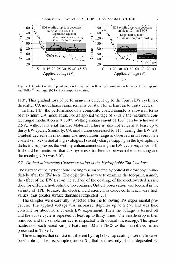
In Fig. 1, EW experiments on the tested samples are presented. The EW testswere performed in dodecane ambient as follows: The applied voltage was increasedfrom 0 V in increments of 2.5 V up to the critical voltage, namely Vs, where CAsaturation sets on. Then the voltage was turned off and the sessile droplet restedback in its initial shape. This will be from now on referred to as an EW cycle.Moreover, robustness verification in terms of dielectric breakdown prevention wasperformed. For this purpose, composite coated samples were compared to Teflon®
coated ones with respect to the CA dependence on applied voltage up to 2.5Vs.Usually, EW experimental data are presented up to the saturation limit, and com-
pared with the predictions of the Young–Lippmann equation. In rare cases andfor relatively thick hydrophobic dielectrics, experimental data for applied voltagesV > Vs are presented [26]. In this work three samples were tested at applied volt-ages apparently beyond the saturation. The samples consist of TEOS as the maindielectric (with thicknesses of 180 and 821 nm) and on top of it the following hy-drophobic top coatings were fabricated: Two composite coatings (with thicknessesof 58 and 174 nm) and one Teflon® coating (52 nm thick).
As expected, the experimental data are in close agreement with the predictionsof Young–Lippmann equation (dashed lines in Fig. 1(a) and (b)) up to the onsetof saturation. In Fig. 1(a), samples of equal TEOS thicknesses and different typesof top coatings (composite and Teflon® coatings) are compared, in terms of CAdependence on the applied voltage. For an applied voltage of 15 V, the contact anglemodulation is 110◦ (from ≈160◦ to ≈50◦) for both samples. However, the EW testsshow that the Teflon® coated sample failed at about 1.4Vs (see arrow in Fig. 1(a)), asbubbles start to emerge from the sample surface. In contrast, the composite coatingsample shows a CA of 37◦ at 44.2 V and a consequent maximum CA modulationof ≈125◦.
The robustness of this composite coating sample was tested at high voltages, upto 2.5Vs. We did not notice any sample failure indication (e.g., electrolysis) duringthis test, however, CA modulation gradually decreases from a maximum of 125◦ to
J. Adhesion Sci. Technol. (2011) DOI:10.1163/156856111X600226 7
(a) (b)
Figure 1. Contact angle dependence on the applied voltage, (a) comparison between the compositeand Teflon® coatings, (b) for the composite coating.
110◦. This gradual loss of performance is evident up to the fourth EW cycle andthereafter CA modulation range remains constant for at least up to thirty cycles.
In Fig. 1(b), the performance of a composite coated sample is shown in termsof maximum CA modulation. For an applied voltage of 74.8 V the maximum con-tact angle modulation is ≈130◦. Wetting enhancement of 130◦ can be achieved at2.5Vs, without material failure. Material failure is also not evident at least up tothirty EW cycles. Similarly, CA modulation decreased to 115◦ during this EW test.Gradual decrease in maximum CA modulation range is observed in all compositecoated samples tested at high voltages. Possibly charge trapping in the hydrophobicdielectric suppresses the wetting enhancement during the EW cycle sequence [14].It should be mentioned that CA hysteresis (difference between the advancing andthe receding CA) was ≈5◦.
3.2. Optical Microscopy Characterization of the Hydrophobic Top Coatings
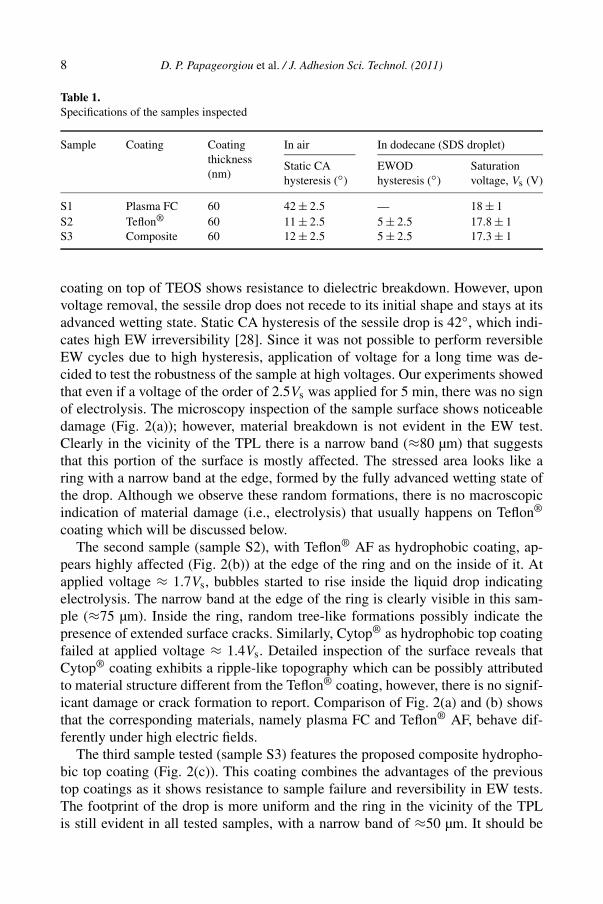
The surface of the hydrophobic coating was inspected by optical microscopy, imme-diately after the EW tests. The objective here was to examine the footprint, namelythe effect of the EW test on the surface of the coating, of the electrowetted sessiledrop for different hydrophobic top coatings. Optical observation was focused in thevicinity of TPL, because the electric field strength is expected to reach very highvalues, thus greater surface damage is expected [27].
The samples were carefully inspected after the following EW experimental pro-cedure: The applied voltage was increased stepwise up to 2.5Vs and was heldconstant for about 30 s at each EW experiment. Then the voltage is turned offand the above cycle is repeated at least up to thirty times. The sessile drop is thenremoved and the sample surface is inspected with optical microscopy. The speci-fications of each tested sample featuring 300 nm TEOS as the main dielectric arepresented in Table 1.
Three samples that consist of different hydrophobic top coatings were fabricated(see Table 1). The first sample (sample S1) that features only plasma-deposited FC
8 D. P. Papageorgiou et al. / J. Adhesion Sci. Technol. (2011)
Table 1.Specifications of the samples inspected
Sample Coating Coatingthickness(nm)
In air In dodecane (SDS droplet)
Static CA EWOD Saturationhysteresis (◦) hysteresis (◦) voltage, Vs (V)
S1 Plasma FC 60 42 ± 2.5 — 18 ± 1S2 Teflon® 60 11 ± 2.5 5 ± 2.5 17.8 ± 1S3 Composite 60 12 ± 2.5 5 ± 2.5 17.3 ± 1
coating on top of TEOS shows resistance to dielectric breakdown. However, uponvoltage removal, the sessile drop does not recede to its initial shape and stays at itsadvanced wetting state. Static CA hysteresis of the sessile drop is 42◦, which indi-cates high EW irreversibility [28]. Since it was not possible to perform reversibleEW cycles due to high hysteresis, application of voltage for a long time was de-cided to test the robustness of the sample at high voltages. Our experiments showedthat even if a voltage of the order of 2.5Vs was applied for 5 min, there was no signof electrolysis. The microscopy inspection of the sample surface shows noticeabledamage (Fig. 2(a)); however, material breakdown is not evident in the EW test.Clearly in the vicinity of the TPL there is a narrow band (≈80 µm) that suggeststhat this portion of the surface is mostly affected. The stressed area looks like aring with a narrow band at the edge, formed by the fully advanced wetting state ofthe drop. Although we observe these random formations, there is no macroscopicindication of material damage (i.e., electrolysis) that usually happens on Teflon®
coating which will be discussed below.The second sample (sample S2), with Teflon® AF as hydrophobic coating, ap-
pears highly affected (Fig. 2(b)) at the edge of the ring and on the inside of it. Atapplied voltage ≈ 1.7Vs, bubbles started to rise inside the liquid drop indicatingelectrolysis. The narrow band at the edge of the ring is clearly visible in this sam-ple (≈75 µm). Inside the ring, random tree-like formations possibly indicate thepresence of extended surface cracks. Similarly, Cytop® as hydrophobic top coatingfailed at applied voltage ≈ 1.4Vs. Detailed inspection of the surface reveals thatCytop® coating exhibits a ripple-like topography which can be possibly attributedto material structure different from the Teflon® coating, however, there is no signif-icant damage or crack formation to report. Comparison of Fig. 2(a) and (b) showsthat the corresponding materials, namely plasma FC and Teflon® AF, behave dif-ferently under high electric fields.
The third sample tested (sample S3) features the proposed composite hydropho-bic top coating (Fig. 2(c)). This coating combines the advantages of the previoustop coatings as it shows resistance to sample failure and reversibility in EW tests.The footprint of the drop is more uniform and the ring in the vicinity of the TPLis still evident in all tested samples, with a narrow band of ≈50 µm. It should be
J. Adhesion Sci. Technol. (2011) DOI:10.1163/156856111X600226 9
(a) (b)
(c)
Figure 2. The effect of the EW tests on sample surfaces for (a) plasma FC coating, (b) Teflon® coatingand (c) composite coating.
mentioned that the sample remains fully functional at least up to thirty EW cy-cles. The inspection of the surface revealed the absence of dendritic patterns seenin sample S2, although the upper layer is the same, i.e., Teflon® AF.
It should be noted that when electrolysis occurs, bubbles are localized in thevicinity of the TPL, confirming the high electric field strength in this region. Theplasma-deposited FC interlayer might have a twofold advantage: on the one handreduced void density between the hydrophobic coating and TEOS through betteradhesion and on the other hand inhibition of local charge trapping in the overall hy-drophobic top coating through reduced porosity. In the following section we focuson the interlayer mechanical properties of the hydrophobic dielectric to estimate thecontribution of these factors to the overall EW system performance.
3.3. Nanoscratch Tests
Nanoscratch tests can provide a measure of the scratch resistance of the hydropho-bic dielectric. Initially, nanoindentation tests were conducted to determine thehardness and elastic modulus of hydrophobic dielectric layers. The correspondingvalues for each layer were used to determine the sequence parameters for the fol-lowing scratch tests, i.e., applied normal load (NL), scratch length, tip velocity. Twosamples were tested. Sample S3 consists of 300 nm TEOS and 60 nm composite
10 D. P. Papageorgiou et al. / J. Adhesion Sci. Technol. (2011)
top coating, namely, 30 nm spin-coated Teflon® on top of 30 nm plasma-depositedFC; sample S2 consists of 300 nm TEOS and 60 nm spin-coated Teflon®.
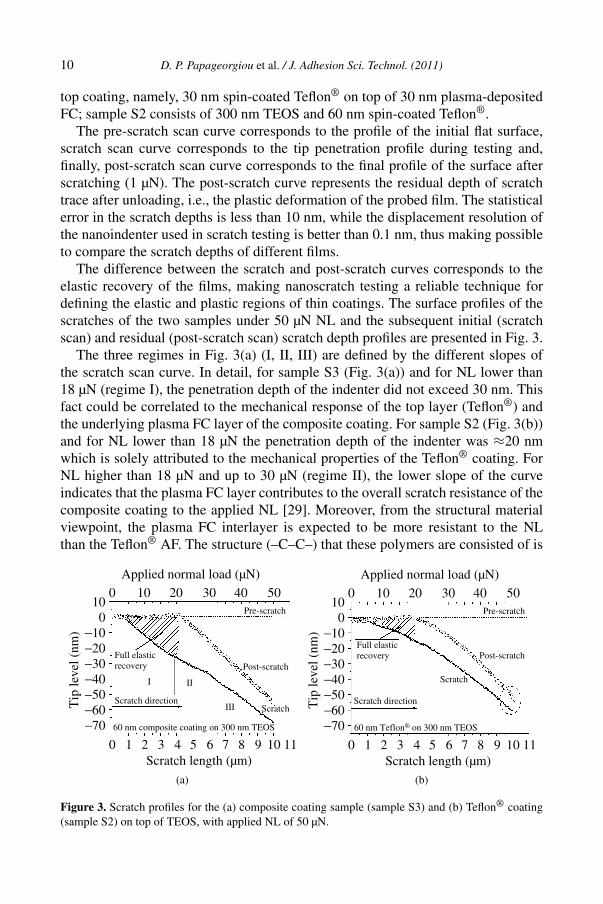
The pre-scratch scan curve corresponds to the profile of the initial flat surface,scratch scan curve corresponds to the tip penetration profile during testing and,finally, post-scratch scan curve corresponds to the final profile of the surface afterscratching (1 µN). The post-scratch curve represents the residual depth of scratchtrace after unloading, i.e., the plastic deformation of the probed film. The statisticalerror in the scratch depths is less than 10 nm, while the displacement resolution ofthe nanoindenter used in scratch testing is better than 0.1 nm, thus making possibleto compare the scratch depths of different films.
The difference between the scratch and post-scratch curves corresponds to theelastic recovery of the films, making nanoscratch testing a reliable technique fordefining the elastic and plastic regions of thin coatings. The surface profiles of thescratches of the two samples under 50 µN NL and the subsequent initial (scratchscan) and residual (post-scratch scan) scratch depth profiles are presented in Fig. 3.
The three regimes in Fig. 3(a) (I, II, III) are defined by the different slopes ofthe scratch scan curve. In detail, for sample S3 (Fig. 3(a)) and for NL lower than18 µN (regime I), the penetration depth of the indenter did not exceed 30 nm. Thisfact could be correlated to the mechanical response of the top layer (Teflon®) andthe underlying plasma FC layer of the composite coating. For sample S2 (Fig. 3(b))and for NL lower than 18 µN the penetration depth of the indenter was ≈20 nmwhich is solely attributed to the mechanical properties of the Teflon® coating. ForNL higher than 18 µN and up to 30 µN (regime II), the lower slope of the curveindicates that the plasma FC layer contributes to the overall scratch resistance of thecomposite coating to the applied NL [29]. Moreover, from the structural materialviewpoint, the plasma FC interlayer is expected to be more resistant to the NLthan the Teflon® AF. The structure (–C–C–) that these polymers are consisted of is
(a) (b)
Figure 3. Scratch profiles for the (a) composite coating sample (sample S3) and (b) Teflon® coating(sample S2) on top of TEOS, with applied NL of 50 µN.
J. Adhesion Sci. Technol. (2011) DOI:10.1163/156856111X600226 11
related to material hardness [30]. Chemical characterization of the plasma FC filmsthrough composition (XPS) analysis has shown that the plasma-deposited F/C ratiois 1.5 [31], whereas the F/C ratio of Teflon is 2. Hence, plasma-deposited FC ismore crosslinked than the Teflon® AF (more (–C–C–) bonds per volume). As aresult, it is not surprising that the plasma-deposited FC appears to be more resistantto the NL.
Comparing the surface profiles in Fig. 3(a) and (b), up to 20 µN of applied NL,the recovered scratch depth of the sample S3 is close to 30 nm, whereas the re-covered scratch depth of the sample S2 is about 15 nm (hatched areas in Fig. 3(a)and (b)). The higher elastic recovery under the same NL suggests that the compos-ite coating can sustain higher scratch induced stresses (higher scratch resistance,i.e., improved adhesion strength) than the Teflon® coating [29]. After NL ≈30 µN(regime III) both samples exhibited elastoplastic behaviour, with sample S2 exhibit-ing almost full plastic behavior (convergence of the initial and the residual scratchprofiles) in the last few nanometers of displacement (indicated in Fig. 3(b) with adashed circle).
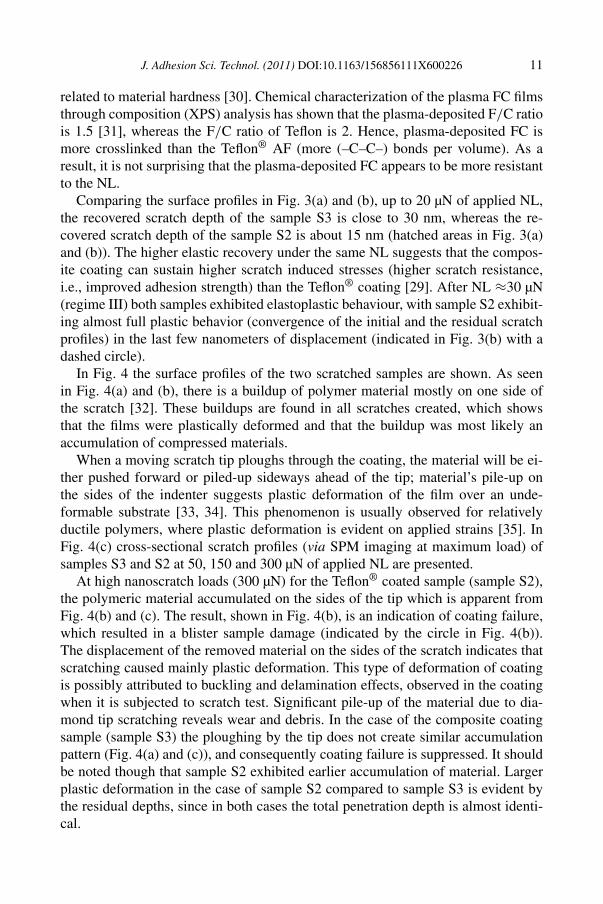
In Fig. 4 the surface profiles of the two scratched samples are shown. As seenin Fig. 4(a) and (b), there is a buildup of polymer material mostly on one side ofthe scratch [32]. These buildups are found in all scratches created, which showsthat the films were plastically deformed and that the buildup was most likely anaccumulation of compressed materials.
When a moving scratch tip ploughs through the coating, the material will be ei-ther pushed forward or piled-up sideways ahead of the tip; material’s pile-up onthe sides of the indenter suggests plastic deformation of the film over an unde-formable substrate [33, 34]. This phenomenon is usually observed for relativelyductile polymers, where plastic deformation is evident on applied strains [35]. InFig. 4(c) cross-sectional scratch profiles (via SPM imaging at maximum load) ofsamples S3 and S2 at 50, 150 and 300 µN of applied NL are presented.
At high nanoscratch loads (300 µN) for the Teflon® coated sample (sample S2),the polymeric material accumulated on the sides of the tip which is apparent fromFig. 4(b) and (c). The result, shown in Fig. 4(b), is an indication of coating failure,which resulted in a blister sample damage (indicated by the circle in Fig. 4(b)).The displacement of the removed material on the sides of the scratch indicates thatscratching caused mainly plastic deformation. This type of deformation of coatingis possibly attributed to buckling and delamination effects, observed in the coatingwhen it is subjected to scratch test. Significant pile-up of the material due to dia-mond tip scratching reveals wear and debris. In the case of the composite coatingsample (sample S3) the ploughing by the tip does not create similar accumulationpattern (Fig. 4(a) and (c)), and consequently coating failure is suppressed. It shouldbe noted though that sample S2 exhibited earlier accumulation of material. Largerplastic deformation in the case of sample S2 compared to sample S3 is evident bythe residual depths, since in both cases the total penetration depth is almost identi-cal.
12 D. P. Papageorgiou et al. / J. Adhesion Sci. Technol. (2011)
(a) (b)
(c)
Figure 4. Scratched surface profiles: SPM images at 50, 100 and 300 µN of applied NL for (a) com-posite coating sample (sample S3), (b) Teflon® coated sample (sample S2). (c) Cross-sectional shapesat maximum applied NL of 50, 100 and 300 µN, i.e., at the end of scratch. Pointing arrow defines thescratch direction of the tip. (Zero level on the vertical axis corresponds to the level of the unscratchedflat surface.)
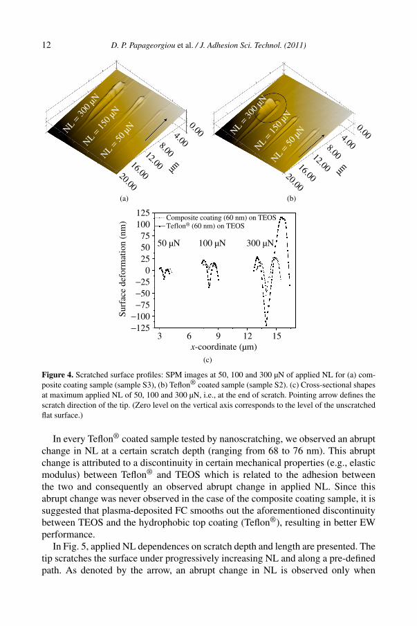
In every Teflon® coated sample tested by nanoscratching, we observed an abruptchange in NL at a certain scratch depth (ranging from 68 to 76 nm). This abruptchange is attributed to a discontinuity in certain mechanical properties (e.g., elasticmodulus) between Teflon® and TEOS which is related to the adhesion betweenthe two and consequently an observed abrupt change in applied NL. Since thisabrupt change was never observed in the case of the composite coating sample, it issuggested that plasma-deposited FC smooths out the aforementioned discontinuitybetween TEOS and the hydrophobic top coating (Teflon®), resulting in better EWperformance.
In Fig. 5, applied NL dependences on scratch depth and length are presented. Thetip scratches the surface under progressively increasing NL and along a pre-definedpath. As denoted by the arrow, an abrupt change in NL is observed only when
J. Adhesion Sci. Technol. (2011) DOI:10.1163/156856111X600226 13
Figure 5. Applied normal load dependences on the scratch length and scratch depth for samples S3and S2. The arrow indicates the onset of critical load. The inset is a magnification of the area depictedby the dashed line.
Teflon® coating is used, which is indicative of strength weakening due to materialheterogeneity [21, 29, 36]; this occurs at a critical scratch length of ≈5.5 µm andNL ≈ 150 µN.
The scratch depth variation (see Fig. 5), indicates that the NL abrupt change setsin when the tip penetration is close to the Teflon®/TEOS interface (sample S2). Thecorresponding critical load is usually denoted as Lc. The existence of an Lc is anindication of failure in terms of coating cracking, delamination or brittle fracturecaused by scratch testing [37]. High elasticity in combination with low hardnessof the Teflon® top coating mostly favors delamination and not coating cracking orbrittle fracture. Moreover, the Teflon® coating of the tested sample is approximately60 nm thick which is close to the scratch depth value where the critical load appears.This strain mismatch evident by the abrupt change in the applied NL induces filmdelamination, and is not observed in the case of the composite coating. We suspectthat the interlayer of plasma FC suitably bonds the oxide substrate and the spin-coated Teflon® layer, therefore the corresponding nanoscratch curve in Fig. 5 issmoother for the composite coating.
4. Conclusions
In this work the effect of plasma-deposited fluorocarbons, as structural layersof the top coating, on EW performance was investigated. A sandwich-like hy-drophobic top coating was fabricated, here called composite coating, comprisinga thin plasma-deposited FC layer and a thin spin-coated Teflon® layer. This sam-
14 D. P. Papageorgiou et al. / J. Adhesion Sci. Technol. (2011)
ple showed resistance to dielectric breakdown, improved CA modulation and re-versibility for at least up to thirty EW cycles, at applied voltages apparently beyondthe saturation. Optical microscopy inspection revealed absence of dendritic patternsusually observed in Teflon® coatings. Nanoscrach testing was conducted to furtherinvestigate the interlayer mechanical properties of the proposed hydrophobic di-electric stack. Nanoscratch measurements showed improved adhesion strength ofthe composite coating to the oxide substrate compared to the equivalent Teflon®
coating sample, confirming the observed improved robustness in EW tests.
Acknowledgements
The research leading to these results received funding from the European Re-search Council under the European Community’s Seventh Framework Programme(FP7/2007-2013)/ERC Grant agreement No. (240710). The authors wish to thankDrs E. Gogolides and A. Tserepi at the Institute of Microelectronics, NCSR‘Demokritos’, for their expert advice in plasma-deposited fluorocarbon films andcleanroom processing. The authors also wish to thank Drs Panagiota Petrou andSotirios Kakabakos from the Institute of Radioisotopes and Radiodiagnostic Prod-ucts of NCSR ‘Demokritos’ for providing access to their optical microscope. Theauthors would like to thank Prof. T. Krupenkin and Dr J. Ashley Taylor of theUniversity of Wisconsin–Madison for kindly providing samples with Cytop® hy-drophobic top coating.
References
1. F. Mugele, Soft Matter 5, 3377 (2009).2. R. B. Fair, Microfluid Nanofluid 3, 245 (2007).3. E. M. Miller and A. R. Wheeler, Anal. Bioanal. Chem. 393, 419 (2009).4. B. Berge and J. Peseux, Eur. Phys. J. E 3, 159 (2000).5. S. Kuiper and B. H. W. Hendriks, Appl. Phys. Lett. 85, 1128 (2004).6. R. A. Hayes and B. J. Feenstra, Nature 425, 383 (2003).7. J. Heikenfeld, K. Zhou, E. Kreit, B. Raj, S. Yang, B. Sun, A. Milarcik, L. Clapp and R. Schwartz,
Nature Photonics 3, 292 (2009).8. V. A. Lifton, J. A. Taylor, B. Vyas, P. Kolodner, R. Cirelli, N. Basavanhally, A. Papazian,
R. Frahm, S. Simon and T. Krupenkin, Appl. Phys. Lett. 93, 043112 (2008).9. S. Berry, J. Kedzierski and B. Abedian, J. Colloid Interface Sci. 303, 517 (2006).
10. E. Seyrat and R. A. Hayes, J. Appl. Phys. 90, 1383 (2001).11. C. Quilliet and B. Berge, Curr. Opin. Colloid Interface Sci. 6, 34 (2001).12. A. G. Papathanasiou and A. G. Boudouvis, Appl. Phys. Lett. 86, 164102 (2005).13. A. I. Drygiannakis, A. G. Papathanasiou and A. G. Boudouvis, Langmuir 25, 147 (2009).14. H. J. J. Verheijen and M. W. J. Prins, Langmuir 15, 6616 (1999).15. M. Vallet, M. Vallade and B. Berge, Eur. Phys. J. B 11, 583 (1999).16. A. G. Papathanasiou, A. T. Papaioannou and A. G. Boudouvis, J. Appl. Phys. 103, 034901 (2008).17. P. Bayiati, A. Tserepi, P. S. Petrou, S. E. Kakabakos, K. Misiakos and E. Gogolides, J. Appl. Phys.
101, 103306 (2007).
J. Adhesion Sci. Technol. (2011) DOI:10.1163/156856111X600226 15
18. H. Moon, S. K. Cho, R. L. Garrell and C. J. Kim, J. Appl. Phys. 92, 4080 (2002).19. A. Datta, I. Y. Eom, A. Dhar, P. Kuban, R. Manor, I. Ahmad, S. Gangopadhyay, T. Dallas,
M. Holtz, F. Temkin and P. K. Dasgupta, IEEE Sensors J. 3, 788 (2003).20. K. Takahashi, T. Mitamura, K. Ono, Y. Setsuhara, A. Itoh and K. Tachibana, Appl. Phys. Lett. 82,
2476 (2003).21. B. R. Kim and M. J. Ko, Thin Solid Films 517, 3216 (2009).22. K. L. Mittal, in: Adhesion Measurement of Films and Coatings, K. L. Mittal (Ed.), pp. 1–13. VSP,
Utrecht (1995).23. DuPont, Teflon® AF Amorphous Fluoropolymer, Product Information (2006).24. C. A. Charitidis, Int. J. Ref. Met. Hard Mater. 28, 51 (2010).25. A. Tserepi, in: Plasma Processes and Polymers, R. D’Agostino (Ed.), p. 51. Wiley-VCH, Wein-
heim (2005).26. M. Paneru, C. Priest, R. Sedev and J. Ralston, J. Phys. Chem. C 114, 8383 (2010).27. F. Mugele and J. C. Baret, J. Phys.: Condens. Matter 17, R705 (2005).28. P. Bayiati, A. Tserepi, D. Goustouridis, K. Misiakos and E. Gogolides, in: Proceedings of the 1st
Europ. Conf. on Microfluidics, Bologna, Italy (2008).29. Y. Liu, T. Zhang, G. Zhang, X. Niu, Z. Song, G. Min, Y. Lin, J. Zhang, W. Zhou, J. Zhang, J. Chu,
Y. Wan and S. Feng, Jpn. J. Appl. Phys. 48, 101601 (2009).30. A. Itoh, A. Inokuchi, S. Yasuda, A. Teramoto, T. Goto, M. Hirayama and T. Ohmi, Jpn. J. Appl.
Phys. 47, 2515 (2008).31. P. Bayiati, A. Tserepi, P. S. Petrou, K. Misiakos, S. E. Kakabakos, E. Gogolides and C. Cardinaud,
Microelectron. Eng. 84, 1677 (2007).32. H. Nie, M. Walzak and N. McIntyre, Appl. Surface Sci. 253, 2320 (2006).33. H. Jiang, R. Browning and H. J. Sue, Polymer 50, 4056 (2009).34. B. Bhushan (Ed.), Scanning Probe Microscopy in Nanoscience and Nanotechnology. Springer,
New York (2009).35. J. A. Sauer and K. D. Pae, Colloid Polym. Sci. 252, 680 (1974).36. J. Ye, N. Kojima, K. Ueoka, J. Shimanuki, T. Nasuno and S. Ogawa, J. Appl. Phys. 95, 3704
(2004).37. X. W. Zhang, L. J. Hu and D. Z. Sun, Acta Mater. 54, 5469 (2006).
Related Documents