Evaluating the Effects of Cache Redundancy on Profit Abhishek Das + , Berkin Ozisikyilmaz + , Serkan Ozdemir + , Gokhan Memik + , Joseph Zambreno * and Alok Choudhary + + Electrical Engineering and Computer Science Department Northwestern University Evanston, IL USA {a-das, berkin, s-ozdemir, g-memik, a-choudhary}@northwestern.edu * Electrical and Computer Engineering Department Iowa State University Ames, IA USA [email protected] ABSTRACT Previous works in computer architecture have mostly neglected revenue and/or profit, key factors driving any design decision. In this paper, we evaluate architectural techniques to optimize for revenue/profit. The continual trend of technology scaling and sub- wavelength lithography has caused transistor feature sizes to shrink into the nanoscale range. As a result, the effects of process variations on critical path delay and chip yields have amplified. A common concept to remedy the effects of variations is speed- binning, by which chips from a single batch are rated by a discrete range of frequencies and sold at different prices. An efficient binning distribution thus decides the profitability of the chip manufacturer. We propose and evaluate a cache-redundancy scheme called substitute cache, which allows the chip manufacturers to modify the number of chips in different bins. Particularly, this technique introduces a small fully associative array associated with each cache way to replicate the data elements that will be stored in the high latency lines, and hence can be effectively used to boost up the overall chip yield and also shift the chip binning distribution towards higher frequencies. We also develop models based on linear regression and neural networks to accurately estimate the chip prices from their architectural configurations. Using these estimation models, we find that our substitute cache scheme can potentially increase the revenue for the batch of chips by as much as 13.1%. * Keywords: Device Variability, Process Variations, Cache Architecture, Profit and Revenue, Fault-tolerance. 1. ITRODUCTIO The research literature is filled with architectural optimizations that seek to improve various design goals such as performance, power consumption, reliability, and security. However, the evaluation of these concepts tends to neglect one of the key factors driving any chip manufacturing decision: a company's bottom-line of revenue or profit. This shortcoming is understandable, as the relationship between any design metric and profit is hard to measure. For example, an optimization that improves performance by 10% will increase profit if a) this increase is valuable/desirable to the consumers, b) the cost of re-engineering can be amortized over the lifespan of the chip, and c) consequent changes in other design factors do * This work was supported in part by NSF grants CNS-0551639, IIS- 0536994, CCF-0747201, CCF-0541337, and OCI-0724599; DoE CAREER Award DEFG02-05ER25691; and by Wissner-Slivka Chair funds. not decrease the value to the consumers. Therefore, it may not be possible to estimate the impact of an architectural optimization on revenue precisely. However, in this paper we will show that we can make accurate estimations on relative impact of different architectural configurations on revenue, and argue that these estimations should be considered during the design of the processor architectures. There are two important aspects of profitability: cost and revenue. To increase profit, one could reduce the cost. Chip yield is one obvious scope for optimization in nanoscale processors [30], as the continuing downward scaling of transistor feature sizes has made fabrication considerably more difficult and expensive [26, 28, 50]. However, to get a better understanding of the impact of an architectural scheme, one needs to understand the effects on revenue as well. For example, an approach that optimizes solely for yield would not take into account the fact that CPUs concurrently manufactured using a single process are routinely sold at different speed ratings and prices. This practice of speed-binning (Figure 1a) is usually performed by testing each manufactured chip separately over a range of frequency levels until it fails. As a result of the inherent process variations, different processors fall into separate speed bins, where they are rated and marketed differently. Speed-binning thus helps the chip manufacturer create a complete product line from a single design. Figure 1b shows an example price distribution representing the Intel Core Duo processor family [16]. Assuming a simplified supply and demand model, the total chip revenue would be the sum of the segmented areas under the yield curve. Consequently, one way of increasing revenue would be to shift the binning distribution in such a way that more processors are able to fall into higher-priced bins. Previous studies have shown that as transistors are reduced in size, it becomes harder to control variations in device parameters such as channel length, gate width, oxide thickness, and device threshold voltage. Even in a relatively mature technology like 90nm, these variations are known to result in as much as a 30% change in chip frequency and 20x change in leakage power [5]. For sub 45nm technologies, parameter variations are expected to be even higher [49]. An expected continuation of this trend will increase the impact of speed-binning on a manufacturer's bottom-line.

Welcome message from author
This document is posted to help you gain knowledge. Please leave a comment to let me know what you think about it! Share it to your friends and learn new things together.
Transcript
Evaluating the Effects of Cache Redundancy on Profit
Abhishek Das+, Berkin Ozisikyilmaz+, Serkan Ozdemir+, Gokhan Memik+, Joseph Zambreno∗ and Alok Choudhary+
+Electrical Engineering and Computer Science Department Northwestern University
Evanston, IL USA {a-das, berkin, s-ozdemir, g-memik,
a-choudhary}@northwestern.edu
*Electrical and Computer Engineering Department Iowa State University
Ames, IA USA [email protected]
ABSTRACT
Previous works in computer architecture have mostly neglected
revenue and/or profit, key factors driving any design decision. In
this paper, we evaluate architectural techniques to optimize for
revenue/profit. The continual trend of technology scaling and sub-
wavelength lithography has caused transistor feature sizes to
shrink into the nanoscale range. As a result, the effects of process
variations on critical path delay and chip yields have amplified. A
common concept to remedy the effects of variations is speed-
binning, by which chips from a single batch are rated by a
discrete range of frequencies and sold at different prices. An
efficient binning distribution thus decides the profitability of the
chip manufacturer. We propose and evaluate a cache-redundancy
scheme called substitute cache, which allows the chip
manufacturers to modify the number of chips in different bins.
Particularly, this technique introduces a small fully associative
array associated with each cache way to replicate the data
elements that will be stored in the high latency lines, and hence
can be effectively used to boost up the overall chip yield and also
shift the chip binning distribution towards higher frequencies. We
also develop models based on linear regression and neural
networks to accurately estimate the chip prices from their
architectural configurations. Using these estimation models, we
find that our substitute cache scheme can potentially increase the
revenue for the batch of chips by as much as 13.1%.*
Keywords: Device Variability, Process Variations, Cache
Architecture, Profit and Revenue, Fault-tolerance.
1. I'TRODUCTIO'
The research literature is filled with architectural optimizations that seek to improve various design goals such as performance, power consumption, reliability, and security. However, the evaluation of these concepts tends to neglect one of the key factors driving any chip manufacturing decision: a company's bottom-line of revenue or profit. This shortcoming is understandable, as the relationship between any design metric and profit is hard to measure. For example, an optimization that improves performance by 10% will increase profit if a) this increase is valuable/desirable to the consumers, b) the cost of re-engineering can be amortized over the lifespan of the chip, and c) consequent changes in other design factors do
*This work was supported in part by NSF grants CNS-0551639, IIS-0536994, CCF-0747201, CCF-0541337, and OCI-0724599; DoE CAREER Award DEFG02-05ER25691; and by Wissner-Slivka Chair funds.
not decrease the value to the consumers. Therefore, it may not be possible to estimate the impact of an architectural optimization on revenue precisely. However, in this paper we will show that we can make accurate estimations on relative impact of different architectural configurations on revenue, and argue that these estimations should be considered during the design of the processor architectures.
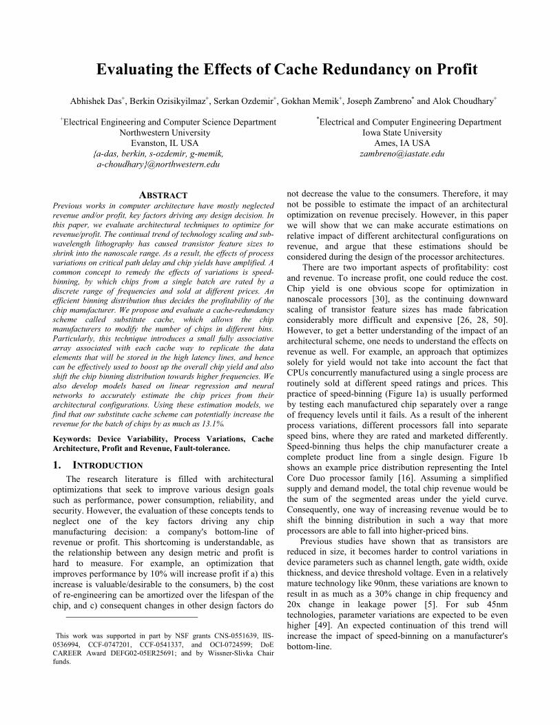
There are two important aspects of profitability: cost and revenue. To increase profit, one could reduce the cost. Chip yield is one obvious scope for optimization in nanoscale processors [30], as the continuing downward scaling of transistor feature sizes has made fabrication considerably more difficult and expensive [26, 28, 50]. However, to get a better understanding of the impact of an architectural scheme, one needs to understand the effects on revenue as well. For example, an approach that optimizes solely for yield would not take into account the fact that CPUs concurrently manufactured using a single process are routinely sold at different speed ratings and prices. This practice of speed-binning (Figure 1a) is usually performed by testing each manufactured chip separately over a range of frequency levels until it fails. As a result of the inherent process variations, different processors fall into separate speed bins, where they are rated and marketed differently. Speed-binning thus helps the chip manufacturer create a complete product line from a single design. Figure 1b shows an example price distribution representing the Intel Core Duo processor family [16]. Assuming a simplified supply and demand model, the total chip revenue would be the sum of the segmented areas under the yield curve. Consequently, one way of increasing revenue would be to shift the binning distribution in such a way that more processors are able to fall into higher-priced bins.
Previous studies have shown that as transistors are reduced in size, it becomes harder to control variations in device parameters such as channel length, gate width, oxide thickness, and device threshold voltage. Even in a relatively mature technology like 90nm, these variations are known to result in as much as a 30% change in chip frequency and 20x change in leakage power [5]. For sub 45nm technologies, parameter variations are expected to be even higher [49]. An expected continuation of this trend will increase the impact of speed-binning on a manufacturer's bottom-line.
In this paper, we propose a cache architecture that aims to improve overall revenue and profit with post-fabrication modifications. Particularly, in this scheme, the level 1 (L1) cache is augmented with a small Substitute Cache (SC) storing the most critical cache words whose latencies may have been affected by process variations. With the help of minimal control logic, the processor can fetch data from SC instead of the main data array whenever a read/write access is made to these critical words. Hence, access latency is minimized with no extra cache misses.
(a)
(b)
Figure 1. (a) Frequency binning in modern microprocessors. (b) Price vs. frequency of Intel Core Duo mobile family (as of
January 2008).
We concentrate on caches because they have been shown to be the critical component under process variations [15]. Also, our analysis (described in Section 4) reveals that the critical path lies on the cache in 58.9% of the chips we model. The reasons for this behavior are three-fold. First, caches consume a relatively large percentage of chip area. Second, L1 caches have a high frequency requirement and consequently tend to utilize low threshold voltages [4]. Finally, according to the “FMAX” model introduced by Bowman et al. [6], a unit which has a high ratio of independent critical paths (Ncp) to critical path logic depth (Lcp) will have a greater variance to mean ratio in its delay distribution, leading to an increased variability due to process effects. SRAM structures have a high number of critical paths with low logic depths in those paths, making them susceptible to process variations.
Although our technique will affect various design stages, such changes remain minimal. Therefore, the proposed technique will have minimal impact on cost. Variable production costs will remain low, as the testing
phase can be incorporated into current binning processes. On the other hand, the proposed scheme will have a significant impact on the binning distribution. As we describe in Section 7, we simulated the effects of process variations on yield and binning distribution using SPICE. We also develop models based on linear regression and neural networks that can be used to estimate the price of a chip using its architectural properties. Using the binning results and our price estimation models, we show that applying our SC scheme to current processor architectures could lead to a potential 13.1% increase in revenue in the most optimistic case.
The remainder of this paper is organized as follows. In the following section, we perform a literature survey of the related works. The details of SC scheme are then described in Section 3. Section 4 talks about the methodology we used for modeling and measuring the effect of process variations on a representative processor architecture. Section 5 describes how we model the binning strategy, while Section 6 discusses the methodologies we developed for price estimation. Experimental results detailing the effect of our approach on binning distribution and revenue are presented in Section 7. Finally, Section 8 concludes the paper with a brief summary.
2. BACKGROU'D A'D RELATED WORK
Variability in process technologies has been extensively studied. In this section, we present brief overviews of the prior works that are proposed to mitigate effects of parameter variations, ranging from architectural to circuit-level techniques. Cache Redundancy schemes:
Several cache redundancy schemes have been proposed [7, 18, 27, 39, 41]. These techniques have been/could be used to reduce the critical delay of a cache. Victim caches [18] are extra level of caches used to hold blocks evicted from a CPU cache due to a conflict or capacity miss. A substitute cache storing the slower blocks of the cache is orthogonal to a victim cache, which stores blocks evicted from the cache. Sohi [41] shows that cache redundancy can be used to prevent yield loss, using a similar concept to our proposed SC. Shivakumar et al. [39] introduce a new yield metric and propose the utilization of redundant structures to increase it. Similarly, techniques like sparing DRAMS and Chipkill are used in Sun’s UltraSPARC T1 processor [7]. Cache redundancy is also present in commercial processors like Itanium, which uses extra banks to improve fault tolerance [27]. Finally, Romanescu et al. [38] propose prefetching data into fast buffers to address Process Variations in L1 caches as well as prioritizing critical instructions to utilize fast registers/functional units. Compared to these alternatives, our SC scheme introduces considerably lower cost in terms of area and latency. Circuit level techniques:
Previous works show that several circuit-level techniques could be adopted to counter the negative effects of process variations [5, 9, 12, 33, 36, 41]. The inter- and intra-die
Yield
lossBin 0 Bin 1 Bin 2
Yield
loss
Frequency
Bin 3
# of chips
chips lost
for high
leakage
chips
lost for
high
delay
Bin 4
241 241
294
423
637
0
100
200
300
400
500
600
700
1.66 1.83 2 2.16 2.33
Pri
ce (
$)
Frequency (GHz)
process variations and their effects on circuit leakage is studied in detail by Rao et al. [35]. In another work, Rao et al. [34] analyze the impact of process variations on circuit leakage and propose methods to reduce them. Most of these techniques focus on analyzing the design statistically or by using static timing analysis, and then modifying the parts of the circuits that are most susceptible to variations. Liang et al. have proposed a variation-tolerant 3 transistor, 1 diode on-chip dynamic memory as a substitute for the traditional 6 transistor SRAM [24]. Many gate-sizing strategies have been used on the critical or near-critical regions of the circuit in order to reduce the effective latency [10, 51]. Although these techniques increase the overall yield, no analysis of the impact on binning has been done.
Performance binning has also been discussed as a means for increasing yield [5, 12, 36]. Datta et al. [12] propose a novel approach of changing the effective speed-binning by gate sizing, and thus increasing the profit. Unlike our schemes, most of their analyses are based on statistical estimations of yield, and the optimizations are for high-level synthesis. Kim et al. [20] have studied the effects of cache size on leakage and analyzed the tradeoff on access time when multiple threshold voltages are used for L1 and L2 caches. In contrast, we perform the replication within the cache and also present a detailed implementation. Variation-tolerant architectural schemes:
Ozdemir et al. [30] present microarchitectural schemes that improve the overall chip yield under process variations to as much as 97%. The authors have shown how powering down sections of the cache can increase the effective yield. Our work, on the other hand encompasses extra redundancy in L1 caches to facilitate efficient binning and profit maximization. Besides, our model includes the entire processor pipeline, as opposed to only L1 caches. Techniques for mitigating the effects of process variations by using variable latency register files and execution units have been proposed by Liang et al. [23]. In a recent work, Liang et al. [25] have studied the effectiveness of post fabrication techniques like voltage interpolations and variable latency in different pipeline loops. Besides, Agarwal et al. [1] propose a scheme that prevents yield loss due to failures in the SRAM cells of the cache. Their approach is mostly based on Built-In Self-Test (BIST) circuitry and the cache optimizations are concentrated towards yield maximization. Teodorescu et al. [46] use variation-aware instruction scheduling and power management to reduce the overall energy delay product and increase throughput of chip multiprocessors. Tiwari et al. [48], on the other hand, propose ReCycle to balance the delay variations between different pipeline stages due to process variations by utilizing a skewed clock. This way, they achieve a processor clock frequency that is equivalent to the average frequency of all pipeline stages instead of the lowest one. They also propose a method to convert the slack in faster stages into power savings. Lee et al. [22] discusses a new metric involving yield, area, and performance for evaluating the tradeoff between yield and
performance in caches. In comparison to the abovementioned works, our efforts are directed towards efficient binning and revenue optimization for set associative caches. In addition, most of the previous techniques listed above have performance implications, i.e., different chips in a frequency bin may exhibit varying performance levels (due to a variation in the IPC). However, our SC scheme provides the same performance (constant IPC) for all the chips in a frequency bin. Other works:
There has been plethora of studies analyzing cache resizing for different goals such as minimizing power consumption or increasing performance. Selective Cache Ways by Albonesi [2] is one of the first works in cache resizing and optimizing energy dissipation of the cache. Flautner et al. [13] have proposed a drowsy cache architecture, which takes into account the state of a cache line and correspondingly changes its mode. The concept of cache decay, on the other hand, exploits the usage information of each cache line in order to turn them off when they are not in use to save leakage power [19]. Yang et al. [52] have analyzed the effects of various cache resizing schemes on reducing the energy-delay of deep submicron processors. Powell et al. [32] have introduced the Gated-Vdd approach, by which the supply voltage is turned off in the unused SRAM cells to save leakage energy. Finally, Tadas and Chakrabarti have developed a scheme in which the adjacent micro-blocks of a cache are resized depending on the hit and miss rate [44]. All these resizing schemes are very effective in reducing the cache leakage and energy, but to the best of our knowledge no resizing schemes have been applied to alter speed-binning and profit.
3. THE SUBSTITUTE CACHE SCHEME
In this section, we describe our proposed cache redundancy technique called Substitute Cache (SC), which masks the effects of process variations by including extra storage in the L1 cache. Particularly, in this scheme each way of the L1 cache is augmented with a fully associative data array, which stores the most critical lines as a result of process variations. Once the SC holds high-delay words, they are never accessed from the main array, allowing the L1 cache to run at higher frequencies. In addition to shifting more chips towards high-priced bins, this scheme also reduces yield losses due to delay violations.
3.1 Architecture
The core idea behind the architecture of SC is to augment each cache way with extra storage that will be used if certain locations in the main cache exhibit long latencies. In such cases, the data will be read from the SC, and chips from the lower frequency bins can now be placed in higher frequency bins, because the high latency lines are not used. Moreover, some of the chips that would have failed due to high access latencies will be added to the overall yield.
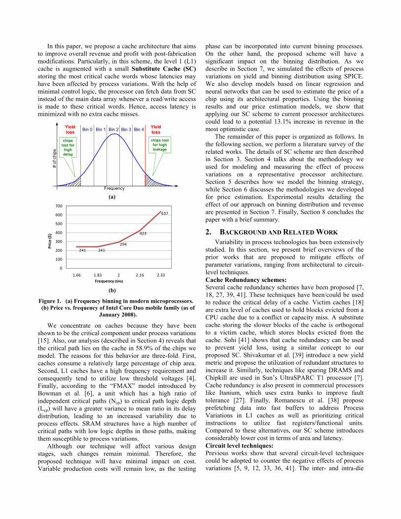
The anatomy of the proposed cache architecture is shown in Figure 2. SC is highlighted within the dashed block. For the sake of clarity, we detail the use of SC on a single cache way; however, each cache way has a similar SC associated with it. SC is similar to a fully-associative cache structure. In our study, its size is either 4 or 8 entries. As opposed to the L1 cache, SC has smaller line sizes. Particularly, it consists of only 64-bit entries, because it stores words of the main data array. Instead of storing the whole cache line, only the critical word in the line is stored in the SC, because our study reveals that the words with maximum access latency are always the ones that are furthest from the decoder. As a result, by just storing these words, we obtain the same improvement in cache frequency while keeping the SC size small. However, if necessary, words in other locations can also be placed into the SC. An SC is divided into 2 components: an index table and a data array. Note that the SC uses the column multiplexers and output drivers of the main array. Whenever a cache word is placed in the data array of the SC, index bits of its address, which is equal to the sum of the row and column addresses (10 bits in our architecture) are placed in the index table of the SC. For example, if we decide to place the word with index value 0x044 to the SC, we will have an entry in the index table with value 0x044. Note that this word would have resided in the row with index 0x8 in the main array with the column address being equal to 0x4. In case of a data access, the index table is checked with the index bits of the address. A match implies that the data will be read from the SC instead of the main array. Specifically, if the index of the address is found in the SC index table, the contents of the corresponding data array row are forwarded to the column multiplexers of the main array. The additional control logic shown in Figure 2 will then set the column multiplexers correctly. If the index of the address does not match any index table entries, the main array will be accessed. Note that, even if there is a match in the index table, the access can still miss in the cache if the corresponding tag does not match. However, the tag structure is not affected by the addition of the SC. If there is a miss due to tag mismatch, we will still output the data, which will be ignored because the tag will indicate the miss. Overall, the tag match/mismatch is independent of the SC design. We only care whether the corresponding parts of the address match with the values stored in the index table so that we can decide whether to supply the data from the main array or the SC.
Now let us consider a typical read operation in the main array. The row address part of the index field selects the appropriate row in the data array through the row decoder. The appropriate word is then chosen by the column multiplexers with the help of the column address bits of the index. One of the key observations is the difference between the times taken by each of these steps. Particularly, the inputs to the column multiplexers are available at the same time the decoder is accessed. However, the signals provided to the decoders will traverse through the decoder
logic, the word lines, the memory cell, the bit lines, and the sense amplifiers before it will reach the column multiplexers. We utilize this imbalance to operate our SC structure. As soon as the address is available, we start accessing the SC index table. If a hit is recorded, we change the input to the column multiplexers to 0. In other words, we forward the output of the SC as the output of the cache. If, on the other hand, there is no match in the index table, we will set the column multiplexer to the original position indicated by the column address. If the time to check the index table in the SC is less than the delay of the data array (the sum of the delays of the decoder, word line, memory cell, bit line, and sense amplifier), then, this operation does not cause any delay overhead on the cache, because while the data array is accessed, we would have already determined the hit/miss in the SC index table. As we will discuss in the next section, this is indeed the case. Hence, the addition of the SC structure does not cause any significant increase in the critical path latency of the cache.
Figure 2. One cache way of a 32KB 4-way set associative L1 cache with Substitute Cache. Column muxes are shaded as
they select data from 9 inputs as opposed to 8 inputs
Similar to a read operation, a write access (either a store operation or write operation during the replacement of a cache line) selects the appropriate index using the row and column addresses and updates the selected word in the cache way selected by the way-select logic. For L1 caches augmented with SC, the index of the data word to be written is searched within the SC index table. If there is a match, the new data word is loaded in the data array of the SC. We must also note that the addition of the SC does not impact the tag (and any related operation including snoop requests).
3.2 Design Issues
Using CACTI 3.2 [40], we found the total access latency for a 8-entry SC to be 0.28 nanoseconds; whereas the latency for the main array (one set of the 32KB 4-way set associative cache) is 0.40 nanoseconds. Therefore, the SC access can be completely overlapped with the main array access and will not cause an increase in the cache
Row Decoder
Tag Index Off
Substitute
Cache L1 Data Banks
64-bit Data Word
DataSelect
(Index match)
Row
Address
ColumnAddress
0
10
DataSelectMux
7
3
1019 3
Data array
128 x
128 b
16
128
64
16 b 16 b 16 b 16 b
IndexTable
10
4
access latency. The only change in the latency of the main array is due to the changes in the column multiplexers. Because of the data forwarding from the SC, the column multiplexers (straddled in Figure 2) have an additional input coming from the SC data array. The analysis with our SPICE model reveals that this overhead is 0.34% of the overall cache access latency. We include this overhead during our binning analysis in Section 7.1. Note that there is no change of CPI for the SC scheme, as the effective cache size remains unchanged. Another point that needs to be mentioned in this context is the susceptibility of the SC to process variations. For this work, we neglect any such impact on the SC since it is much smaller than the L1 cache and its latency is significantly lower, hence it is unlikely to become the critical component.
One of the key components during the operation of SC is the index table. After the chip is manufactured, a Built-In-Self-Test (BIST) is performed where n most critical cache indices are chosen and placed in the SC index table. Note that these values are extracted only once during the lifetime of the chip and never changed. Therefore, they can be extracted by the BIST and become part of the booting process, where they are read from a permanent location and placed into the index table every time the processor boots. It should be noted that the size of the SC dictates the area and power overhead of this approach. With the help of SPICE and CACTI, we found the total power overhead to be 6.0% and 6.5% of the main array for a 4- and 8-entry SC, respectively. These overheads are included during the calculations of the yield losses. The area of the cache increases by 3.7% and 4.1% for the 4- and 8-entry SC, respectively.
4. PROCESS VARIATIO'S A'D ARCHITECTURE
MODELI'G
This section presents a description of the processor and cache models we use in this paper and describes how we model process variations.
4.1 Processor Model
To model a processor core, we have taken into account the 7-stage pipeline in the Alpha-21264 (EV6) architecture. The main critical components of our processor are the Fetch Unit, the Rename Unit, the Issue Queue, the Integer Execution Unit, the Register File, and the L1 Data cache. All these components are modeled in SPICE using the 45nm BPTM technology models [8]. The fetch and rename units are modeled as a combination of 16 fan-out of four (FO4) gates. The issue queue is based on that of the Alpha EV6 and has 20 entries. The register file is an 80-entry structure with 4 read and 2 write ports. The integer execution unit is modeled using the netlist generated after synthesizing the corresponding component in the Sun OpenSPARC code [43]. Our L1 cache is a 32 KB 4-way set associative cache, the model of which is based on the architecture described by Amrutur and Horowitz [3].
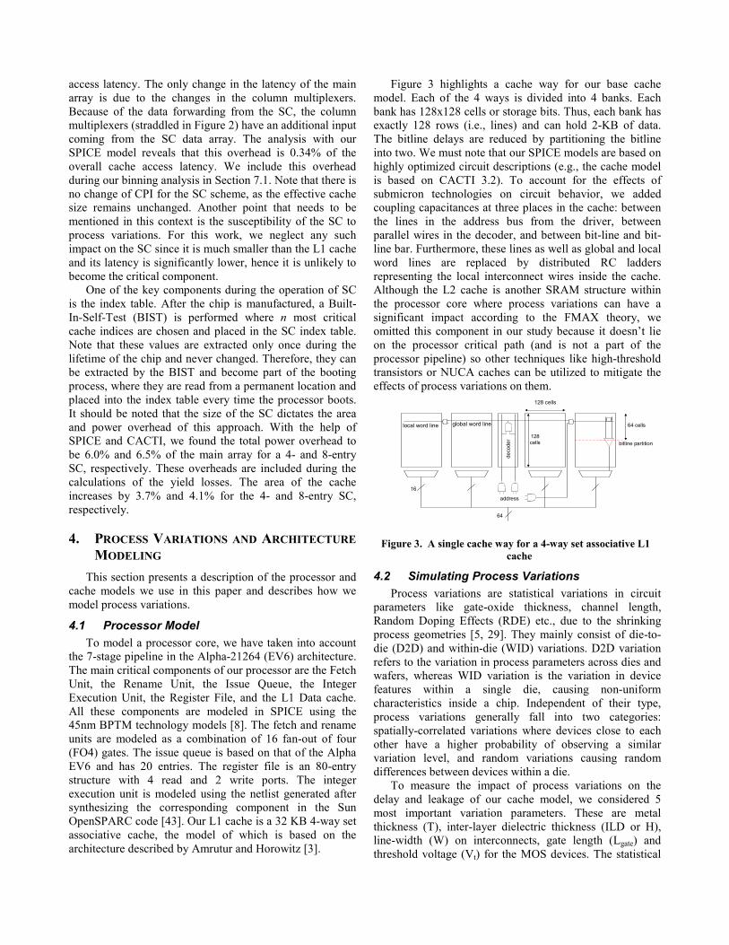
Figure 3 highlights a cache way for our base cache model. Each of the 4 ways is divided into 4 banks. Each bank has 128x128 cells or storage bits. Thus, each bank has exactly 128 rows (i.e., lines) and can hold 2-KB of data. The bitline delays are reduced by partitioning the bitline into two. We must note that our SPICE models are based on highly optimized circuit descriptions (e.g., the cache model is based on CACTI 3.2). To account for the effects of submicron technologies on circuit behavior, we added coupling capacitances at three places in the cache: between the lines in the address bus from the driver, between parallel wires in the decoder, and between bit-line and bit-line bar. Furthermore, these lines as well as global and local word lines are replaced by distributed RC ladders representing the local interconnect wires inside the cache. Although the L2 cache is another SRAM structure within the processor core where process variations can have a significant impact according to the FMAX theory, we omitted this component in our study because it doesn’t lie on the processor critical path (and is not a part of the processor pipeline) so other techniques like high-threshold transistors or NUCA caches can be utilized to mitigate the effects of process variations on them.
Figure 3. A single cache way for a 4-way set associative L1 cache
4.2 Simulating Process Variations
Process variations are statistical variations in circuit parameters like gate-oxide thickness, channel length, Random Doping Effects (RDE) etc., due to the shrinking process geometries [5, 29]. They mainly consist of die-to-die (D2D) and within-die (WID) variations. D2D variation refers to the variation in process parameters across dies and wafers, whereas WID variation is the variation in device features within a single die, causing non-uniform characteristics inside a chip. Independent of their type, process variations generally fall into two categories: spatially-correlated variations where devices close to each other have a higher probability of observing a similar variation level, and random variations causing random differences between devices within a die.
To measure the impact of process variations on the delay and leakage of our cache model, we considered 5 most important variation parameters. These are metal thickness (T), inter-layer dielectric thickness (ILD or H), line-width (W) on interconnects, gate length (Lgate) and threshold voltage (Vt) for the MOS devices. The statistical
decoder
address
16
64
global word linelocal word line
64 cells
128cells bitline partition
64 cells
128 cells
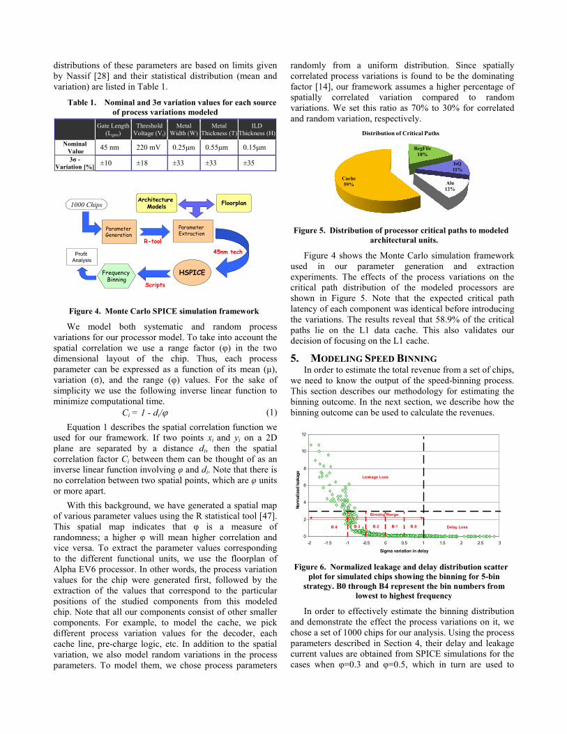
distributions of these parameters are based on limits given by Nassif [28] and their statistical distribution (mean and variation) are listed in Table 1.
Table 1. 'ominal and 3σ variation values for each source
of process variations modeled
Gate Length
(Lgate) Threshold
Voltage (Vt) Metal
Width (W) Metal
Thickness (T) ILD
Thickness (H)
'ominal
Value 45 nm 220 mV 0.25µm 0.55µm 0.15µm
3σ -
Variation [%] ±10 ±18 ±33 ±33 ±35
Figure 4. Monte Carlo SPICE simulation framework
We model both systematic and random process variations for our processor model. To take into account the spatial correlation we use a range factor (φ) in the two dimensional layout of the chip. Thus, each process parameter can be expressed as a function of its mean (µ), variation (σ), and the range (φ) values. For the sake of simplicity we use the following inverse linear function to minimize computational time.
Ci = 1 - di/ϕ (1)
Equation 1 describes the spatial correlation function we used for our framework. If two points xi and yi on a 2D plane are separated by a distance di, then the spatial correlation factor Ci between them can be thought of as an inverse linear function involving φ and di. Note that there is no correlation between two spatial points, which are φ units or more apart.
With this background, we have generated a spatial map of various parameter values using the R statistical tool [47]. This spatial map indicates that φ is a measure of randomness; a higher φ will mean higher correlation and vice versa. To extract the parameter values corresponding to the different functional units, we use the floorplan of Alpha EV6 processor. In other words, the process variation values for the chip were generated first, followed by the extraction of the values that correspond to the particular positions of the studied components from this modeled chip. Note that all our components consist of other smaller components. For example, to model the cache, we pick different process variation values for the decoder, each cache line, pre-charge logic, etc. In addition to the spatial variation, we also model random variations in the process parameters. To model them, we chose process parameters
randomly from a uniform distribution. Since spatially correlated process variations is found to be the dominating factor [14], our framework assumes a higher percentage of spatially correlated variation compared to random variations. We set this ratio as 70% to 30% for correlated and random variation, respectively.
Figure 5. Distribution of processor critical paths to modeled architectural units.
Figure 4 shows the Monte Carlo simulation framework used in our parameter generation and extraction experiments. The effects of the process variations on the critical path distribution of the modeled processors are shown in Figure 5. Note that the expected critical path latency of each component was identical before introducing the variations. The results reveal that 58.9% of the critical paths lie on the L1 data cache. This also validates our decision of focusing on the L1 cache.
5. MODELI'G SPEED BI''I'G In order to estimate the total revenue from a set of chips,
we need to know the output of the speed-binning process. This section describes our methodology for estimating the binning outcome. In the next section, we describe how the binning outcome can be used to calculate the revenues.
Figure 6. 'ormalized leakage and delay distribution scatter plot for simulated chips showing the binning for 5-bin
strategy. B0 through B4 represent the bin numbers from
lowest to highest frequency
In order to effectively estimate the binning distribution and demonstrate the effect the process variations on it, we chose a set of 1000 chips for our analysis. Using the process parameters described in Section 4, their delay and leakage current values are obtained from SPICE simulations for the cases when φ=0.3 and φ=0.5, which in turn are used to
Parameter Generation
HSPICEFrequency Binning
Parameter Extraction
Floorplan
R-tool
Scripts
1000 Chips
45nm tech
Architecture Models
Profit
Analysis
0
2
4
6
8
10
12
-2 -1.5 -1 -0.5 0 0.5 1 1.5 2 2.5 3
Sigma variation in delay
Norm
alized leakage
Binning Range
B 4 B 3 B 2 B 1 B 0
Leakage Loss
Delay Loss
RegFile
18%
IsQ
11%
Alu
12%
Cache
59%
Distribution of Critical Paths
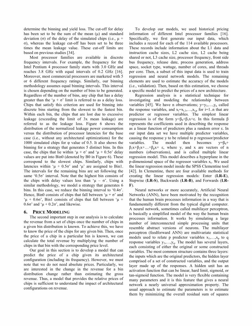
determine the binning and yield loss. The cut-off for delay has been set to be the sum of the mean (µ) and standard deviation (σ) of the delay of the simulated chips (i.e., µ + σ), whereas the leakage cut-off has been set to be three times the mean leakage value. These cut-off limits are based on previous studies [34].
Most processor families are available in discrete frequency intervals. For example, the frequency for the Intel Pentium 4 processor family starts with 3.0 GHz and reaches 3.8 GHz with equal intervals of 0.2 GHz [16]. Moreover, most commercial processors are marketed with 5 or 6 different frequency ratings. Similarly, our binning methodology assumes equal binning intervals. This interval is chosen depending on the number of bins to be generated. Regardless of the number of bins, any chip that has a delay greater than the ‘µ + σ’ limit is referred to as a delay loss. Chips that satisfy this criterion are used for binning into discrete bins starting from the slowest to the fastest bin. Within each bin, the chips that are lost due to excessive leakage (exceeding the limit of 3x mean leakage) are referred to as the leakage loss. Figure 6 shows the distribution of the normalized leakage power consumption versus the distribution of processor latencies for the base case (i.e., without any architectural optimizations) for the 1000 simulated chips for φ value of 0.5. It also shows the binning for a strategy that generates 5 distinct bins. In this case, the chips that lie within ‘µ + σ’ and ‘µ + 0.5σ’ delay values are put into Bin0 (denoted by B0 in Figure 6). These correspond to the slowest chips. Similarly, chips with latencies within ‘µ + 0.5σ’ and ‘µ’ are assigned to Bin1. The intervals for the remaining bins are set following the same ‘0.5σ’ interval. Note that the highest bin consists of the chips with delay values less than ‘µ – σ’. Using a similar methodology, we model a strategy that generates 6 bins. In this case, we reduce the binning interval to ‘0.4σ’. Hence, Bin0 consists of chips that fall between ‘µ + σ’ and ‘µ + 0.6σ’, Bin1 consists of chips that fall between ‘µ + 0.6σ’ and ‘µ + 0.2σ’, and likewise.
6. PRICE MODELI'G The second important step in our analysis is to calculate
the revenue from a set of chips once the number of chips in a given bin distribution is known. To achieve this, we have to know the price of the chips for any given bin. Then, once the price of a chip in a particular bin is known, we can calculate the total revenue by multiplying the number of chips in that bin with the corresponding price level.
Our goal in this section is to develop a model that can predict the price of a chip given its architectural configuration (including its frequency). However, we must note that we do not need absolute prices. Particularly, we are interested in the change in the revenue for a bin distribution change rather than estimating the gross revenue. Thus, a model that provides the relative prices of chips is sufficient to understand the impact of architectural configurations on revenue.
To develop our models, we used historical pricing information of different Intel processor families [16]. Specifically, we first generate our input data, which includes a record for each of the 114 available processors. These records include information about the L1 data and instruction cache sizes, L2 cache size, L2 cache being shared or not, L3 cache size, processor frequency, front side bus frequency, release date, process generation, address space, socket type, wattage, number of cores, and threads per core. Then, a subset of this input data is used to train regression and neural network models. The remaining elements are used to estimate the accuracy of the models (i.e., validation). Then, based on this estimation, we choose a specific model to predict the prices of a new architecture.
Regression analysis is a statistical technique for investigating and modeling the relationship between variables [45]. We have n observations; y=y1,…,yn called the response variables, and xi=xi,1,…,xi,p for i=1..n that are predictor or regressor variables. The simplest linear regression is of the form y=β0+β1x+ε. In this formula β represents the coefficients used in describing the response as a linear function of predictors plus a random error ε. In our input data set we have multiple predictor variables, causing the response y to be related to p regressor/predictor variables. The model then becomes y=β0+ β1x+β2x+…+βpx+ ε, where y, and x are vectors of n numbers (observations), and is called multiple linear regression model. This model describes a hyperplane in the p-dimensional space of the regressor variables xi. We used the linear regression model inside the SPSS Clementine tool [42]. In Clementine, there are four available methods for creating the linear regression models: Enter (LR-E), Stepwise (LR-S), Backwards (LR-B), and Forwards (LR-F).
Neural networks or more accurately, Artificial Neural Networks (ANN), have been motivated by the recognition that the human brain processes information in a way that is fundamentally different from the typical digital computer. A neural network, sometimes called multilayer perceptron, is basically a simplified model of the way the human brain processes information. It works by simulating a large number of interconnected simple processing units that resemble abstract versions of neurons. The multilayer perceptron (feedforward ANN) are multivariate statistical models used to relate p predictor variables x1,…,xp to q response variables y1,…,yq. The model has several layers, each consisting of either the original or some constructed variables. The most common structure contains three layers: the inputs which are the original predictors, the hidden layer comprised of a set of constructed variables, and the output layer made up of the responses. A hidden unit has an activation function that can be linear, hard limit, sigmoid, or tan-sigmoid function. The model is very flexible containing many parameters and it is this feature that gives a neural network a nearly universal approximation property. The usual approach to estimate the parameters is to estimate them by minimizing the overall residual sum of squares
taken over all responses and all observations. This is a nonlinear least-squares problem. Often back-propagation procedure, which is a variation of steepest descent, is used.
We used the SPSS Clementine tool to build the NN models. The neural network node provides six different training methods: Quick (''-Q), Single (''-S) (modified version of Quick), Dynamic (''-D), Multiple (''-M), Prune (''-P) and Exhaustive prune (''-E) method, which is related to the NN-P method.1‡
During our analysis we have grouped the list of processors into three different categories: desktop, mobile, and server. Due to space limitations we only present results for desktop processors; the remaining processor types provide similar results. Rather than using the raw input data directly, we divide our database into ten groups. We randomly leave one group out (test data), and then use the remaining nine groups for model creation and validation, i.e., groups 1 through 8 are used for model creation and group 9 (validation data) is used to estimate the error of the created model; groups 2 through 9 is used for model creation and group 1 (validation data) used for error estimation and so on. Using these nine models, we approximate the error rate by finding the error during the prediction of the test and validation groups. The model with the lowest error is used for estimating the prices. For our input set, the minimum error rate is achieved with the NN-Q method, which provides 1.9% average error rate for the processors in the test data. NN-Q includes 11 out of the 14 predictor variables. The important factors used in the neural network model (with their relative importance presented in parenthesis) are front side bus frequency (0.34), clock frequency (0.30), number of cores (0.22), threads per core (0.14), L2 cache size (0.09) and the release date (0.07), where a relative importance of 0 denotes that the field has no effect on prediction and relative importance of 1.0 denoting that the field completely determines the prediction. We have to note that these importance factors do not need to add up to 1, i.e., the sum can be greater than 1. In our analysis, we generally observe that neural networks outperform the regression methods. One of the reasons is that the price curves are usually sublinear in lower frequency bins and there are rapid increases as we move to higher processor frequencies. The neural network models capture these non-linearities effectively.
These results show that using the subset of the processors available, we can create a very accurate model presenting the relation between the processor properties and its price. In other words, they show that there is a significant correlation between the price of the processor and its configuration, even though markets are also influenced by the preferences of the consumers interacting in it. The existence of such a relation is not surprising, though, as prices of chips are largely determined by their value to the consumers. This value, in turn, depends highly
‡1 Note that we have made our prediction models available for public use [31].
on the performance of the chip, which is strongly tied to its configuration/properties (e.g., performance of a processor can be accurately predicted from its configuration [17, 21]). This forms a link between the configuration of a processor and its price/value. Our models can unveil this relation and accurately estimate the price of a processor from its architectural configuration. We use these models to calculate the revenue results presented in the next section.
7. EXPERIME'TAL RESULTS In this section, we describe the analysis of our proposed
schemes. Section 7.1 describes how our schemes change the outcome of the speed-binning, while Section 7.2 analyzes the impact of these changes on the revenue.
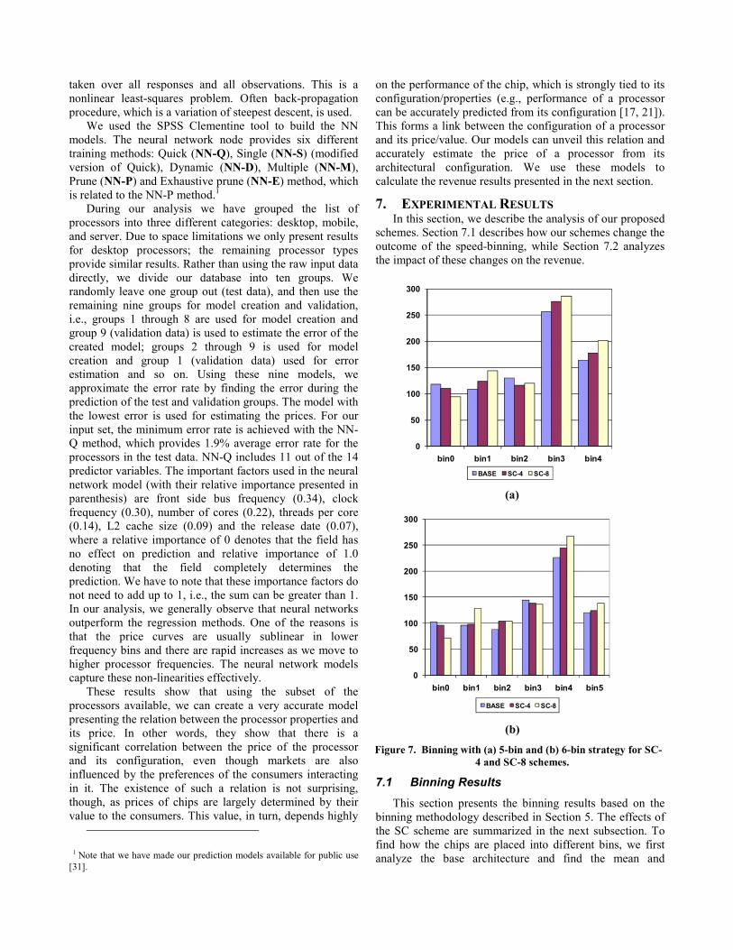
(a)
(b)
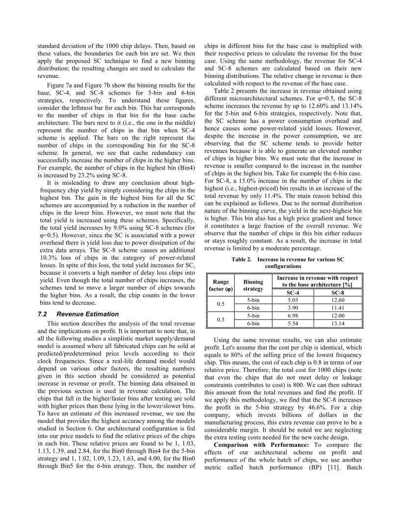
Figure 7. Binning with (a) 5-bin and (b) 6-bin strategy for SC-4 and SC-8 schemes.
7.1 Binning Results
This section presents the binning results based on the binning methodology described in Section 5. The effects of the SC scheme are summarized in the next subsection. To find how the chips are placed into different bins, we first analyze the base architecture and find the mean and
0
50
100
150
200
250
300
bin0 bin1 bin2 bin3 bin4
BASE SC-4 SC-8
0
50
100
150
200
250
300
bin0 bin1 bin2 bin3 bin4 bin5
BASE SC-4 SC-8
standard deviation of the 1000 chip delays. Then, based on these values, the boundaries for each bin are set. We then apply the proposed SC technique to find a new binning distribution; the resulting changes are used to calculate the revenue.
Figure 7a and Figure 7b show the binning results for the base, SC-4, and SC-8 schemes for 5-bin and 6-bin strategies, respectively. To understand these figures, consider the leftmost bar for each bin. This bar corresponds to the number of chips in that bin for the base cache architecture. The bars next to it (i.e., the one in the middle) represent the number of chips in that bin when SC-4 scheme is applied. The bars on the right represent the number of chips in the corresponding bin for the SC-8 scheme. In general, we see that cache redundancy can successfully increase the number of chips in the higher bins. For example, the number of chips in the highest bin (Bin4) is increased by 23.2% using SC-8.
It is misleading to draw any conclusion about high-frequency chip yield by simply considering the chips in the highest bin. The gain in the highest bins for all the SC schemes are accompanied by a reduction in the number of chips in the lower bins. However, we must note that the total yield is increased using these schemes. Specifically, the total yield increases by 9.0% using SC-8 schemes (for φ=0.5). However, since the SC is associated with a power overhead there is yield loss due to power dissipation of the extra data arrays. The SC-8 scheme causes an additional 10.3% loss of chips in the category of power-related losses. In spite of this loss, the total yield increases for SC, because it converts a high number of delay loss chips into yield. Even though the total number of chips increases, the schemes tend to move a larger number of chips towards the higher bins. As a result, the chip counts in the lower bins tend to decrease.
7.2 Revenue Estimation
This section describes the analysis of the total revenue and the implications on profit. It is important to note that, in all the following studies a simplistic market supply/demand model is assumed where all fabricated chips can be sold at predicted/predetermined price levels according to their clock frequencies. Since a real-life demand model would depend on various other factors, the resulting numbers given in this section should be considered as potential increase in revenue or profit. The binning data obtained in the previous section is used in revenue calculation. The chips that fall in the higher/faster bins after testing are sold with higher prices than those lying in the lower/slower bins. To have an estimate of this increased revenue, we use the model that provides the highest accuracy among the models studied in Section 6. Our architectural configuration is fed into our price models to find the relative prices of the chips in each bin. These relative prices are found to be 1, 1.03, 1.13, 1.39, and 2.84, for the Bin0 through Bin4 for the 5-bin strategy and 1, 1.02, 1.09, 1.23, 1.63, and 4.00, for the Bin0 through Bin5 for the 6-bin strategy. Then, the number of
chips in different bins for the base case is multiplied with their respective prices to calculate the revenue for the base case. Using the same methodology, the revenue for SC-4 and SC-8 schemes are calculated based on their new binning distributions. The relative change in revenue is then calculated with respect to the revenue of the base case.
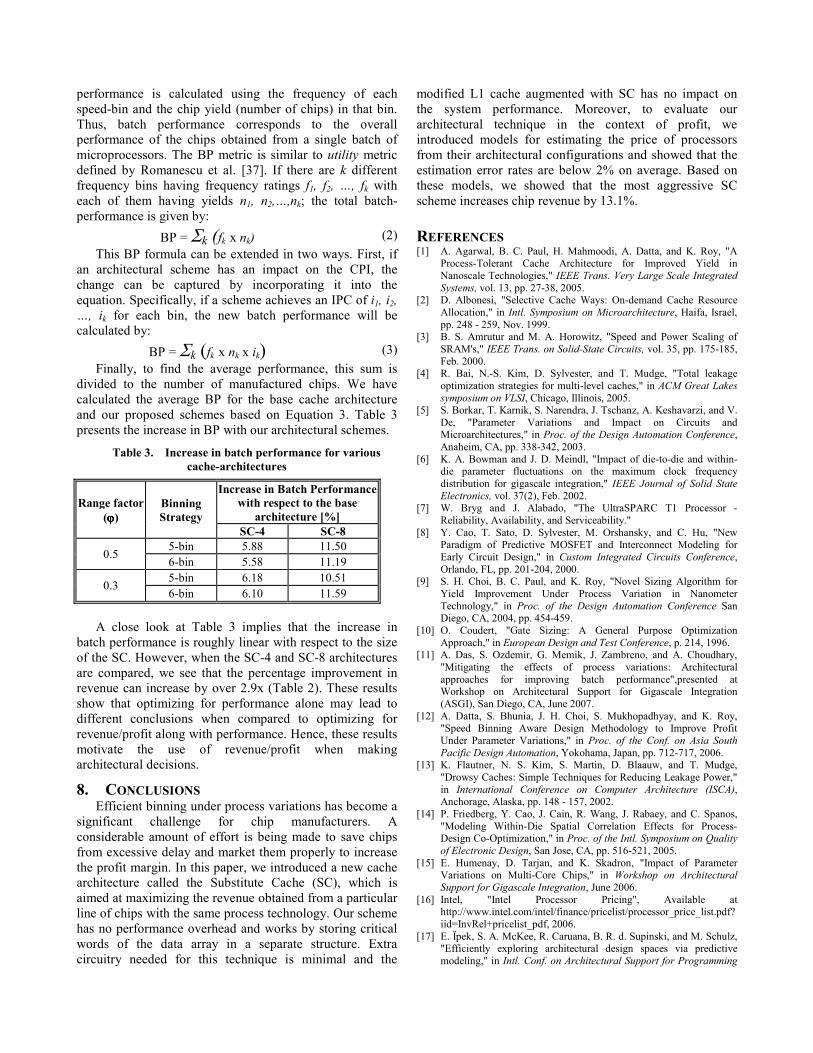
Table 2 presents the increase in revenue obtained using different microarchitectural schemes. For φ=0.5, the SC-8 scheme increases the revenue by up to 12.60% and 13.14% for the 5-bin and 6-bin strategies, respectively. Note that, the SC scheme has a power consumption overhead and hence causes some power-related yield losses. However, despite the increase in the power consumption, we are observing that the SC scheme tends to provide better revenues because it is able to generate an elevated number of chips in higher bins. We must note that the increase in revenue is smaller compared to the increase in the number of chips in the highest bin. Take for example the 6-bin case. For SC-8, a 15.0% increase in the number of chips in the highest (i.e., highest-priced) bin results in an increase of the total revenue by only 11.4%. The main reason behind this can be explained as follows. Due to the normal distribution nature of the binning curve, the yield in the next-highest bin is higher. This bin also has a high price gradient and hence it constitutes a large fraction of the overall revenue. We observe that the number of chips in this bin either reduces or stays roughly constant. As a result, the increase in total revenue is limited by a moderate percentage.
Table 2. Increase in revenue for various SC
configurations
Using the same revenue results, we can also estimate
profit. Let's assume that the cost per chip is identical, which equals to 80% of the selling price of the lowest frequency chip. This means, the cost of each chip is 0.8 in terms of our relative price. Therefore, the total cost for 1000 chips (note that even the chips that do not meet delay or leakage constraints contributes to cost) is 800. We can then subtract this amount from the total revenues and find the profit. If we apply this methodology, we find that the SC-8 increases the profit in the 5-bin strategy by 46.6%. For a chip company, which invests billions of dollars in the manufacturing process, this extra revenue can prove to be a considerable margin. It should be noted we are neglecting the extra testing costs needed for the new cache design.
Comparison with Performance: To compare the effects of our architectural scheme on profit and performance of the whole batch of chips, we use another metric called batch performance (BP) [11]. Batch
Range
factor (ϕϕϕϕ)
Binning
strategy
Increase in revenue with respect
to the base architecture [%]
SC-4 SC-8
0.5 5-bin 5.03 12.60
6-bin 3.90 11.41
0.3 5-bin 6.98 12.00
6-bin 5.54 13.14
performance is calculated using the frequency of each speed-bin and the chip yield (number of chips) in that bin. Thus, batch performance corresponds to the overall performance of the chips obtained from a single batch of microprocessors. The BP metric is similar to utility metric defined by Romanescu et al. [37]. If there are k different frequency bins having frequency ratings f1, f2, …, fk with each of them having yields n1, n2,…,nk; the total batch-performance is given by:
BP = Σk (fk x nk) (2)
This BP formula can be extended in two ways. First, if an architectural scheme has an impact on the CPI, the change can be captured by incorporating it into the equation. Specifically, if a scheme achieves an IPC of i1, i2, …, ik for each bin, the new batch performance will be calculated by:
BP = Σk (fk x nk x ik) (3)
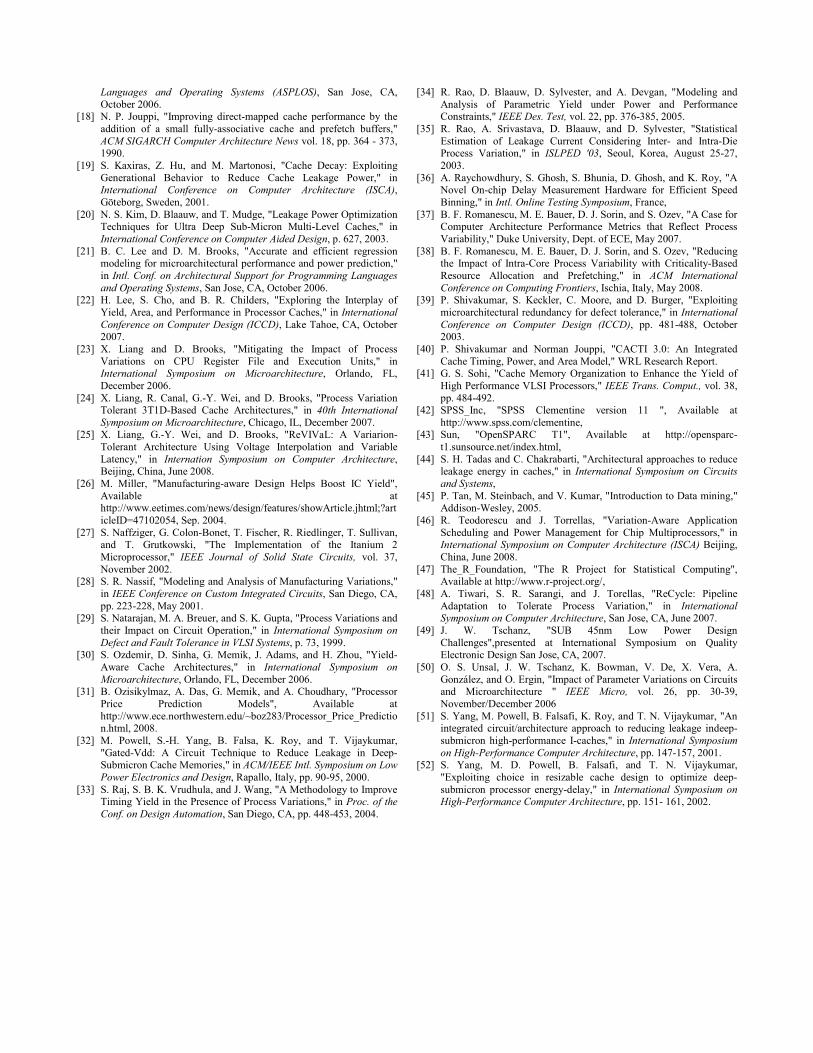
Finally, to find the average performance, this sum is divided to the number of manufactured chips. We have calculated the average BP for the base cache architecture and our proposed schemes based on Equation 3. Table 3 presents the increase in BP with our architectural schemes.
Table 3. Increase in batch performance for various
cache-architectures
A close look at Table 3 implies that the increase in
batch performance is roughly linear with respect to the size of the SC. However, when the SC-4 and SC-8 architectures are compared, we see that the percentage improvement in revenue can increase by over 2.9x (Table 2). These results show that optimizing for performance alone may lead to different conclusions when compared to optimizing for revenue/profit along with performance. Hence, these results motivate the use of revenue/profit when making architectural decisions.
8. CO'CLUSIO'S Efficient binning under process variations has become a
significant challenge for chip manufacturers. A considerable amount of effort is being made to save chips from excessive delay and market them properly to increase the profit margin. In this paper, we introduced a new cache architecture called the Substitute Cache (SC), which is aimed at maximizing the revenue obtained from a particular line of chips with the same process technology. Our scheme has no performance overhead and works by storing critical words of the data array in a separate structure. Extra circuitry needed for this technique is minimal and the
modified L1 cache augmented with SC has no impact on the system performance. Moreover, to evaluate our architectural technique in the context of profit, we introduced models for estimating the price of processors from their architectural configurations and showed that the estimation error rates are below 2% on average. Based on these models, we showed that the most aggressive SC scheme increases chip revenue by 13.1%.
REFERE'CES [1] A. Agarwal, B. C. Paul, H. Mahmoodi, A. Datta, and K. Roy, "A
Process-Tolerant Cache Architecture for Improved Yield in Nanoscale Technologies," IEEE Trans. Very Large Scale Integrated
Systems, vol. 13, pp. 27-38, 2005. [2] D. Albonesi, "Selective Cache Ways: On-demand Cache Resource
Allocation," in Intl. Symposium on Microarchitecture, Haifa, Israel, pp. 248 - 259, Nov. 1999.
[3] B. S. Amrutur and M. A. Horowitz, "Speed and Power Scaling of SRAM's," IEEE Trans. on Solid-State Circuits, vol. 35, pp. 175-185, Feb. 2000.
[4] R. Bai, N.-S. Kim, D. Sylvester, and T. Mudge, "Total leakage optimization strategies for multi-level caches," in ACM Great Lakes
symposium on VLSI, Chicago, Illinois, 2005. [5] S. Borkar, T. Karnik, S. Narendra, J. Tschanz, A. Keshavarzi, and V.
De, "Parameter Variations and Impact on Circuits and Microarchitectures," in Proc. of the Design Automation Conference, Anaheim, CA, pp. 338-342, 2003.
[6] K. A. Bowman and J. D. Meindl, "Impact of die-to-die and within-die parameter fluctuations on the maximum clock frequency distribution for gigascale integration," IEEE Journal of Solid State
Electronics, vol. 37(2), Feb. 2002. [7] W. Bryg and J. Alabado, "The UltraSPARC T1 Processor -
Reliability, Availability, and Serviceability." [8] Y. Cao, T. Sato, D. Sylvester, M. Orshansky, and C. Hu, "New
Paradigm of Predictive MOSFET and Interconnect Modeling for Early Circuit Design," in Custom Integrated Circuits Conference, Orlando, FL, pp. 201-204, 2000.
[9] S. H. Choi, B. C. Paul, and K. Roy, "Novel Sizing Algorithm for Yield Improvement Under Process Variation in Nanometer Technology," in Proc. of the Design Automation Conference San Diego, CA, 2004, pp. 454-459.
[10] O. Coudert, "Gate Sizing: A General Purpose Optimization Approach," in European Design and Test Conference, p. 214, 1996.
[11] A. Das, S. Ozdemir, G. Memik, J. Zambreno, and A. Choudhary, "Mitigating the effects of process variations: Architectural approaches for improving batch performance",presented at Workshop on Architectural Support for Gigascale Integration (ASGI), San Diego, CA, June 2007.
[12] A. Datta, S. Bhunia, J. H. Choi, S. Mukhopadhyay, and K. Roy, "Speed Binning Aware Design Methodology to Improve Profit Under Parameter Variations," in Proc. of the Conf. on Asia South
Pacific Design Automation, Yokohama, Japan, pp. 712-717, 2006. [13] K. Flautner, N. S. Kim, S. Martin, D. Blaauw, and T. Mudge,
"Drowsy Caches: Simple Techniques for Reducing Leakage Power," in International Conference on Computer Architecture (ISCA), Anchorage, Alaska, pp. 148 - 157, 2002.
[14] P. Friedberg, Y. Cao, J. Cain, R. Wang, J. Rabaey, and C. Spanos, "Modeling Within-Die Spatial Correlation Effects for Process-Design Co-Optimization," in Proc. of the Intl. Symposium on Quality
of Electronic Design, San Jose, CA, pp. 516-521, 2005. [15] E. Humenay, D. Tarjan, and K. Skadron, "Impact of Parameter
Variations on Multi-Core Chips," in Workshop on Architectural
Support for Gigascale Integration, June 2006. [16] Intel, "Intel Processor Pricing", Available at
http://www.intel.com/intel/finance/pricelist/processor_price_list.pdf?iid=InvRel+pricelist_pdf, 2006.
[17] E. Ïpek, S. A. McKee, R. Caruana, B. R. d. Supinski, and M. Schulz, "Efficiently exploring architectural design spaces via predictive modeling," in Intl. Conf. on Architectural Support for Programming
Range factor
(ϕϕϕϕ)
Binning
Strategy
Increase in Batch Performance
with respect to the base
architecture [%]
SC-4 SC-8
0.5 5-bin 5.88 11.50 6-bin 5.58 11.19
0.3 5-bin 6.18 10.51
6-bin 6.10 11.59
Languages and Operating Systems (ASPLOS), San Jose, CA, October 2006.
[18] N. P. Jouppi, "Improving direct-mapped cache performance by the addition of a small fully-associative cache and prefetch buffers," ACM SIGARCH Computer Architecture @ews vol. 18, pp. 364 - 373, 1990.
[19] S. Kaxiras, Z. Hu, and M. Martonosi, "Cache Decay: Exploiting Generational Behavior to Reduce Cache Leakage Power," in International Conference on Computer Architecture (ISCA), Göteborg, Sweden, 2001.
[20] N. S. Kim, D. Blaauw, and T. Mudge, "Leakage Power Optimization Techniques for Ultra Deep Sub-Micron Multi-Level Caches," in International Conference on Computer Aided Design, p. 627, 2003.
[21] B. C. Lee and D. M. Brooks, "Accurate and efficient regression modeling for microarchitectural performance and power prediction," in Intl. Conf. on Architectural Support for Programming Languages
and Operating Systems, San Jose, CA, October 2006. [22] H. Lee, S. Cho, and B. R. Childers, "Exploring the Interplay of
Yield, Area, and Performance in Processor Caches," in International
Conference on Computer Design (ICCD), Lake Tahoe, CA, October 2007.
[23] X. Liang and D. Brooks, "Mitigating the Impact of Process Variations on CPU Register File and Execution Units," in International Symposium on Microarchitecture, Orlando, FL, December 2006.
[24] X. Liang, R. Canal, G.-Y. Wei, and D. Brooks, "Process Variation Tolerant 3T1D-Based Cache Architectures," in 40th International
Symposium on Microarchitecture, Chicago, IL, December 2007. [25] X. Liang, G.-Y. Wei, and D. Brooks, "ReVIVaL: A Variarion-
Tolerant Architecture Using Voltage Interpolation and Variable Latency," in Internation Symposium on Computer Architecture, Beijing, China, June 2008.
[26] M. Miller, "Manufacturing-aware Design Helps Boost IC Yield", Available at http://www.eetimes.com/news/design/features/showArticle.jhtml;?articleID=47102054, Sep. 2004.
[27] S. Naffziger, G. Colon-Bonet, T. Fischer, R. Riedlinger, T. Sullivan, and T. Grutkowski, "The Implementation of the Itanium 2 Microprocessor," IEEE Journal of Solid State Circuits, vol. 37, November 2002.
[28] S. R. Nassif, "Modeling and Analysis of Manufacturing Variations," in IEEE Conference on Custom Integrated Circuits, San Diego, CA, pp. 223-228, May 2001.
[29] S. Natarajan, M. A. Breuer, and S. K. Gupta, "Process Variations and their Impact on Circuit Operation," in International Symposium on
Defect and Fault Tolerance in VLSI Systems, p. 73, 1999. [30] S. Ozdemir, D. Sinha, G. Memik, J. Adams, and H. Zhou, "Yield-
Aware Cache Architectures," in International Symposium on
Microarchitecture, Orlando, FL, December 2006. [31] B. Ozisikylmaz, A. Das, G. Memik, and A. Choudhary, "Processor
Price Prediction Models", Available at http://www.ece.northwestern.edu/~boz283/Processor_Price_Prediction.html, 2008.
[32] M. Powell, S.-H. Yang, B. Falsa, K. Roy, and T. Vijaykumar, "Gated-Vdd: A Circuit Technique to Reduce Leakage in Deep-Submicron Cache Memories," in ACM/IEEE Intl. Symposium on Low
Power Electronics and Design, Rapallo, Italy, pp. 90-95, 2000. [33] S. Raj, S. B. K. Vrudhula, and J. Wang, "A Methodology to Improve
Timing Yield in the Presence of Process Variations," in Proc. of the
Conf. on Design Automation, San Diego, CA, pp. 448-453, 2004.
[34] R. Rao, D. Blaauw, D. Sylvester, and A. Devgan, "Modeling and Analysis of Parametric Yield under Power and Performance Constraints," IEEE Des. Test, vol. 22, pp. 376-385, 2005.
[35] R. Rao, A. Srivastava, D. Blaauw, and D. Sylvester, "Statistical Estimation of Leakage Current Considering Inter- and Intra-Die Process Variation," in ISLPED '03, Seoul, Korea, August 25-27, 2003.
[36] A. Raychowdhury, S. Ghosh, S. Bhunia, D. Ghosh, and K. Roy, "A Novel On-chip Delay Measurement Hardware for Efficient Speed Binning," in Intl. Online Testing Symposium, France,
[37] B. F. Romanescu, M. E. Bauer, D. J. Sorin, and S. Ozev, "A Case for Computer Architecture Performance Metrics that Reflect Process Variability," Duke University, Dept. of ECE, May 2007.
[38] B. F. Romanescu, M. E. Bauer, D. J. Sorin, and S. Ozev, "Reducing the Impact of Intra-Core Process Variability with Criticality-Based Resource Allocation and Prefetching," in ACM International
Conference on Computing Frontiers, Ischia, Italy, May 2008. [39] P. Shivakumar, S. Keckler, C. Moore, and D. Burger, "Exploiting
microarchitectural redundancy for defect tolerance," in International
Conference on Computer Design (ICCD), pp. 481-488, October 2003.
[40] P. Shivakumar and Norman Jouppi, "CACTI 3.0: An Integrated Cache Timing, Power, and Area Model," WRL Research Report.
[41] G. S. Sohi, "Cache Memory Organization to Enhance the Yield of High Performance VLSI Processors," IEEE Trans. Comput., vol. 38, pp. 484-492.
[42] SPSS_Inc, "SPSS Clementine version 11 ", Available at http://www.spss.com/clementine,
[43] Sun, "OpenSPARC T1", Available at http://opensparc-t1.sunsource.net/index.html,
[44] S. H. Tadas and C. Chakrabarti, "Architectural approaches to reduce leakage energy in caches," in International Symposium on Circuits
and Systems, [45] P. Tan, M. Steinbach, and V. Kumar, "Introduction to Data mining,"
Addison-Wesley, 2005. [46] R. Teodorescu and J. Torrellas, "Variation-Aware Application
Scheduling and Power Management for Chip Multiprocessors," in International Symposium on Computer Architecture (ISCA) Beijing, China, June 2008.
[47] The_R_Foundation, "The R Project for Statistical Computing", Available at http://www.r-project.org/,
[48] A. Tiwari, S. R. Sarangi, and J. Torellas, "ReCycle: Pipeline Adaptation to Tolerate Process Variation," in International Symposium on Computer Architecture, San Jose, CA, June 2007.
[49] J. W. Tschanz, "SUB 45nm Low Power Design Challenges",presented at International Symposium on Quality Electronic Design San Jose, CA, 2007.
[50] O. S. Unsal, J. W. Tschanz, K. Bowman, V. De, X. Vera, A. González, and O. Ergin, "Impact of Parameter Variations on Circuits and Microarchitecture " IEEE Micro, vol. 26, pp. 30-39, November/December 2006
[51] S. Yang, M. Powell, B. Falsafi, K. Roy, and T. N. Vijaykumar, "An integrated circuit/architecture approach to reducing leakage indeep-submicron high-performance I-caches," in International Symposium
on High-Performance Computer Architecture, pp. 147-157, 2001. [52] S. Yang, M. D. Powell, B. Falsafi, and T. N. Vijaykumar,
"Exploiting choice in resizable cache design to optimize deep-submicron processor energy-delay," in International Symposium on High-Performance Computer Architecture, pp. 151- 161, 2002.
Related Documents


![SP-Cache: Load-Balanced, Redundancy-Free Cluster Caching ...Weiwa/Papers/Sp_cache-sc18.pdffork-join queueing system [12], [13] and establish an upper-bound analysis to quantify the](https://static.cupdf.com/doc/110x72/5eb46215ab7903125c130f0b/sp-cache-load-balanced-redundancy-free-cluster-caching-weiwapapersspcache-sc18pdf.jpg)