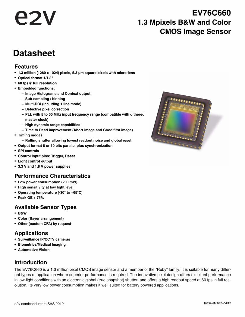
e2v semiconductors SAS 2012 EV76C660 1.3 Mpixels B&W and Color CMOS Image Sensor Datasheet Features • 1.3 million (1280 x 1024) pixels, 5.3 μm square pixels with micro-lens • Optical format 1/1.8" • 60 fps@ full resolution • Embedded functions: – Image Histograms and Context output – Sub-sampling / binning – Multi-ROI (including 1 line mode) – Defective pixel correction – PLL with 5 to 50 MHz input frequency range (compatible with dithered master clock) – High dynamic range capabilities – Time to Read improvement (Abort image and Good first image) • Timing modes: – Rolling shutter allowing lowest readout noise and global reset • Output format 8 or 10 bits parallel plus synchronization • SPI controls • Control input pins: Trigger, Reset • Light control output • 3.3 V and 1.8 V power supplies Performance Characteristics • Low power consumption (200 mW) • High sensitivity at low light level • Operating temperature [-30° to +65°C] • Peak QE > 75% Available Sensor Types • B&W • Color (Bayer arrangement) • Other (custom CFA) by request Applications • Surveillance IP/CCTV cameras • Biometrics/Medical Imaging • Automotive Vision Introduction The EV76C660 is a 1.3 million pixel CMOS image sensor and a member of the “Ruby” family. It is suitable for many differ- ent types of application where superior performance is required. The innovative pixel design offers excellent performance in low-light conditions with an electronic global (true snapshot) shutter, and offers a high readout speed at 60 fps in full res- olution. Its very low power consumption makes it well suited for battery powered applications. 1085A–IMAGE–04/12

Welcome message from author
This document is posted to help you gain knowledge. Please leave a comment to let me know what you think about it! Share it to your friends and learn new things together.
Transcript
EV76C6601.3 Mpixels B&W and Color
CMOS Image Sensor
Datasheet
Features• 1.3 million (1280 x 1024) pixels, 5.3 µm square pixels with micro-lens• Optical format 1/1.8"• 60 fps@ full resolution• Embedded functions:– Image Histograms and Context output– Sub-sampling / binning– Multi-ROI (including 1 line mode)– Defective pixel correction – PLL with 5 to 50 MHz input frequency range (compatible with dithered
master clock)– High dynamic range capabilities– Time to Read improvement (Abort image and Good first image)
• Timing modes:– Rolling shutter allowing lowest readout noise and global reset
• Output format 8 or 10 bits parallel plus synchronization • SPI controls• Control input pins: Trigger, Reset• Light control output • 3.3 V and 1.8 V power supplies
Performance Characteristics• Low power consumption (200 mW)• High sensitivity at low light level• Operating temperature [-30° to +65°C]• Peak QE > 75%
Available Sensor Types• B&W• Color (Bayer arrangement)• Other (custom CFA) by request
Applications• Surveillance IP/CCTV cameras• Biometrics/Medical Imaging• Automotive Vision
IntroductionThe EV76C660 is a 1.3 million pixel CMOS image sensor and a member of the “Ruby” family. It is suitable for many differ-ent types of application where superior performance is required. The innovative pixel design offers excellent performancein low-light conditions with an electronic global (true snapshot) shutter, and offers a high readout speed at 60 fps in full res-olution. Its very low power consumption makes it well suited for battery powered applications.
e2v semiconductors SAS 2012 1085A–IMAGE–04/12
EV76C660
1. Typical Performance Data
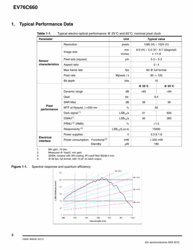
Figure 1-1. Spectral response and quantum efficiency
Table 1-1. Typical electro-optical performance @ 25°C and 65°C, nominal pixel clock
Parameter Unit Typical value
Sensor characteristics
Resolution pixels 1280 (H) × 1024 (V)
Image sizemm
inches
6.9 (H) × 5.5 (V) - 8.7 (diagonal)
≈ 1/1.8
Pixel size (square) µm 5.3 × 5.3
Aspect ratio 5 / 4
Max frame rate fps 60 @ full format
Pixel rate Mpixels / s 90 -> 120
Bit depth bits 10
Pixel performance
@ 25°C @ 65°C
Dynamic range dB >65 >64
Qsat ke- 8.4
SNR Max dB 39 39
MTF at Nyquist, λ=550 nm % 50
Dark signal (1)
1. Min gain, 10 bits.
LSB10/s 31 600
DSNU(1) LSB10/s 30 360
PRNU (2) (RMS)
2. Measured @ Vsat/2, min gain.
% <1.5
Responsivity (3)
3. 3200K, window with AR coating, IR cutoff filter BG38 2 mm.
LSB10/(Lux.s) 15000
Electrical interface
Power supplies V 3.3 & 1.8
Power consumption: Functional (4)
Standby
4. @ 60 fps, full format, with 10 pF on each output.
mW
µW
< 200 mW
180
21085A–IMAGE–04/12
e2v semiconductors SAS 2012
EV76C660
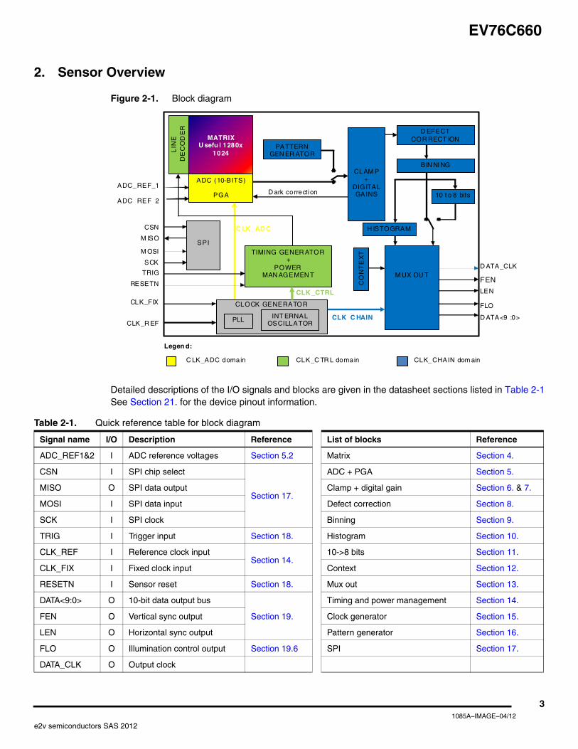
2. Sensor Overview
Figure 2-1. Block diagram
Detailed descriptions of the I/O signals and blocks are given in the datasheet sections listed in Table 2-1See Section 21. for the device pinout information.
CLK_R EF
CLAM P
+ DIGITAL GAINS
MATRIX U sefu l 1280x
1024
ADC (10-BITS)
PGA
D EFECT COR RECT ION
M UX OU T
FLO
H ISTOGRAM
PATTERN GEN ER ATOR
ADC_REF_1
TRIG
D ark correction
BIN NI NG
CO
NT
EX
T
SCK
M ISO
TIMING GENER ATOR +
POWER MAN AGEMEN T
SPI
RESETN
CSN
M OSI
ADC_REF_2
CLK_FIX
10 t o 8 bits
D ATA<9 :0>
FEN
LEN
CLOCK GENERATOR
D ATA_CLK
LIN
E D
EC
OD
ER
INT ERNAL OSCILLATOR PLL CLK_C HAIN
CLK _CTRL
C LK _AD C
C LK_ADC domain CLK_C TR L domain CLK_CHAIN dom ain
Legen d:
Table 2-1. Quick reference table for block diagram
Signal name I/O Description Reference List of blocks Reference
ADC_REF1&2 I ADC reference voltages Section 5.2 Matrix Section 4.
CSN I SPI chip select
Section 17.
ADC + PGA Section 5.
MISO O SPI data output Clamp + digital gain Section 6. & 7.
MOSI I SPI data input Defect correction Section 8.
SCK I SPI clock Binning Section 9.
TRIG I Trigger input Section 18. Histogram Section 10.
CLK_REF I Reference clock inputSection 14.
10->8 bits Section 11.
CLK_FIX I Fixed clock input Context Section 12.
RESETN I Sensor reset Section 18. Mux out Section 13.
DATA<9:0> O 10-bit data output bus
Section 19.
Timing and power management Section 14.
FEN O Vertical sync output Clock generator Section 15.
LEN O Horizontal sync output Pattern generator Section 16.
FLO O Illumination control output Section 19.6 SPI Section 17.
DATA_CLK O Output clock
31085A–IMAGE–04/12
e2v semiconductors SAS 2012
EV76C660
3. Standard Configuration
3.1 Sensor SettingsThe static configuration required to allow image capture is as follows:
• All ground pins connected.
• All power supply pins with the same name connected together.
• SPI pins connected to the host controller.
• 1.8 V pins and 3.3 V pins powered-on.
• Input clock driving the CLK_REF input pin.
• RESETN pin held at high level after the power-on sequence. See Section 18.1.1
• STANDBY state is deactivated by writing 0 in the stdby_rqst bit in the <reg_ctrl_cfg> register. See Section 17.3.8
• Image capture is triggered by a high level on the TRIG pin or setting the trig_rqst bit in the <reg_ctrl_cfg> register. See Section 17.3.8
For improved performance, VDD33A and VDD18A must be noise-free. The best way to decoupleVDD33A and to increase the power supply rejection ratio is to use a linear regulator dedicated to theimage sensor. To prevent noise on VDD18A an inductor can be used.
41085A–IMAGE–04/12
e2v semiconductors SAS 2012
EV76C660
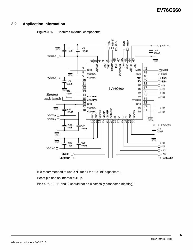
3.2 Application Information
Figure 3-1. Required external components
It is recommended to use X7R for all the 100 nF capacitors.
Reset pin has an internal pull-up.
Pins 4, 6, 10, 11 and12 should not be electrically connected (floating).
EV76C660
51085A–IMAGE–04/12
e2v semiconductors SAS 2012
EV76C660
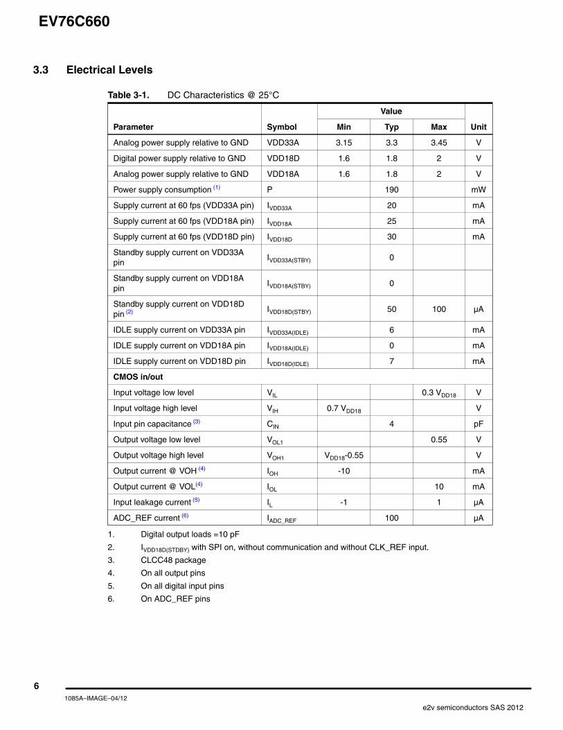
3.3 Electrical Levels
Table 3-1. DC Characteristics @ 25°C
Parameter Symbol
Value
UnitMin Typ Max
Analog power supply relative to GND VDD33A 3.15 3.3 3.45 V
Digital power supply relative to GND VDD18D 1.6 1.8 2 V
Analog power supply relative to GND VDD18A 1.6 1.8 2 V
Power supply consumption (1)
1. Digital output loads =10 pF
P 190 mW
Supply current at 60 fps (VDD33A pin) IVDD33A 20 mA
Supply current at 60 fps (VDD18A pin) IVDD18A 25 mA
Supply current at 60 fps (VDD18D pin) IVDD18D 30 mA
Standby supply current on VDD33A pin
IVDD33A(STBY) 0
Standby supply current on VDD18A pin
IVDD18A(STBY) 0
Standby supply current on VDD18D pin (2)
2. IVDD18D(STDBY) with SPI on, without communication and without CLK_REF input.
IVDD18D(STBY) 50 100 µA
IDLE supply current on VDD33A pin IVDD33A(IDLE) 6 mA
IDLE supply current on VDD18A pin IVDD18A(IDLE) 0 mA
IDLE supply current on VDD18D pin IVDD18D(IDLE) 7 mA
CMOS in/out
Input voltage low level VIL 0.3 VDD18 V
Input voltage high level VIH 0.7 VDD18 V
Input pin capacitance (3)
3. CLCC48 package
CIN 4 pF
Output voltage low level VOL1 0.55 V
Output voltage high level VOH1 VDD18-0.55 V
Output current @ VOH (4)
4. On all output pins
IOH -10 mA
Output current @ VOL(4) IOL 10 mA
Input leakage current (5)
5. On all digital input pins
IL -1 1 µA
ADC_REF current (6)
6. On ADC_REF pins
IADC_REF 100 µA
61085A–IMAGE–04/12
e2v semiconductors SAS 2012
EV76C660
4. Matrix
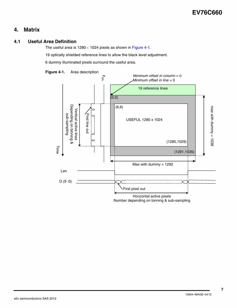
4.1 Useful Area DefinitionThe useful area is 1280 × 1024 pixels as shown in Figure 4-1.
19 optically shielded reference lines to allow the black level adjustment.
6 dummy illuminated pixels surround the useful area.
Figure 4-1. Area description
19 reference lines
max w
ith dumm
y = 1036
Minimum offset in column = 0 Minimum offset in line = 0
Max with dummy = 1292
Len
Horizontal active pixels Number depending on binning & sub-sampling
Vertical active lines
Depending on binning &
sub-sam
pling
D (9 :0)
First pixel out
First line out
(0,0)
Tim
e
(6,6)
(1285,1029)
USEFUL 1280 x 1024
FE
N
(1291,1035)
71085A–IMAGE–04/12
e2v semiconductors SAS 2012
EV76C660
4.2 CFA (Color Filter Array)The following CFA types are implemented:
• Monochrome
• RGB Bayer filter
Other types are available on request.
As CFA choice does not require a silicon hardware change but only post-process, to allow correct config-uration of binning, subsampling and color gains, the sensor must be configured by setting 1 in thecolor_en register when a color sensor is used. Note that image size depends on this factor. See Section4.5.3.1.
RoiX_0l stands for ROI1_0l_1, Roi2_0l_1, Roi3_0l_1 & Roi4_0l_1. See Section 17.3.11, 17.3.12,17.3.13, and 17.3.14 respect
RoiX_0c stands for Roi1_0c_1, Roi2_0c_1, Roi3_0c_1 & Roi4_0c_1. Section 17.3.11, 17.3.12, 17.3.13,and 17.3.14 respectively
It is recommended to keep:
• Roi_W_1 + Roi_0c_2 even
• Roi_h_1 + Roi_0l_2 even
Flip H & Flip V are under roi_flip_h & roi_flip_v control. See <reg_miscel2> in Section 17.3.4
4.3 PixelsThe matrix is composed of five transistor (5T) pixels. This structure supports either global shutter (GS)mode or electronic rolling shutter (ERS) mode (Section 18.2).
4.4 Lens CRA (Chief Ray Angle) compensation.In order to better focus the light rays on the photodiode, the EV76C660 micro lenses are radially shiftedto match the exit angles due to the external application lens. This results in improved efficiency andreduced corner shading.
Table 4-1. Color of first pixel using the flip functions (depends on H&V offset parities)
RoiX_0l_1 / RoiX_0c_1
Flip H Flip V Odd/Odd Odd/Even Even/odd Even/Even
N N Red Green Red Green Blue Blue
N O Green Blue Blue Red Green Red
O N Green Red Red Blue Green Blue
O O Blue Green Blue Green Red Red
81085A–IMAGE–04/12
e2v semiconductors SAS 2012
EV76C660
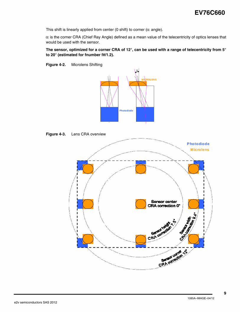
This shift is linearly applied from center (0 shift) to corner (α angle).
α is the corner CRA (Chief Ray Angle) defined as a mean value of the telecentricity of optics lenses thatwould be used with the sensor.
The sensor, optimized for a corner CRA of 12°, can be used with a range of telecentricity from 5°to 20° (estimated for fnumber f#/1.2).
Figure 4-2. Microlens Shifting
Figure 4-3. Lens CRA overview
α
Photodiode
MICROLENS
Photodiode
Microlens
91085A–IMAGE–04/12
e2v semiconductors SAS 2012
EV76C660
4.5 Region Of Interest (ROI)
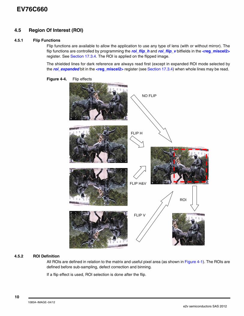
4.5.1 Flip FunctionsFlip functions are available to allow the application to use any type of lens (with or without mirror). Theflip functions are controlled by programming the roi_flip_h and roi_flip_v bitfields in the <reg_miscel2>register. See Section 17.3.4. The ROI is applied on the flipped image.
The shielded lines for dark reference are always read first (except in expanded ROI mode selected bythe roi_expanded bit in the <reg_miscel2> register (see Section 17.3.4) when whole lines may be read.
Figure 4-4. Flip effects
4.5.2 ROI DefinitionAll ROIs are defined in relation to the matrix and useful pixel area (as shown in Figure 4-1). The ROIs aredefined before sub-sampling, defect correction and binning.
If a flip effect is used, ROI selection is done after the flip.
FLIP V
NO FLIP
FLIP H&V
FLIP H
ROI
101085A–IMAGE–04/12
e2v semiconductors SAS 2012
EV76C660
4.5.3 Sub-Sampling and Windowing
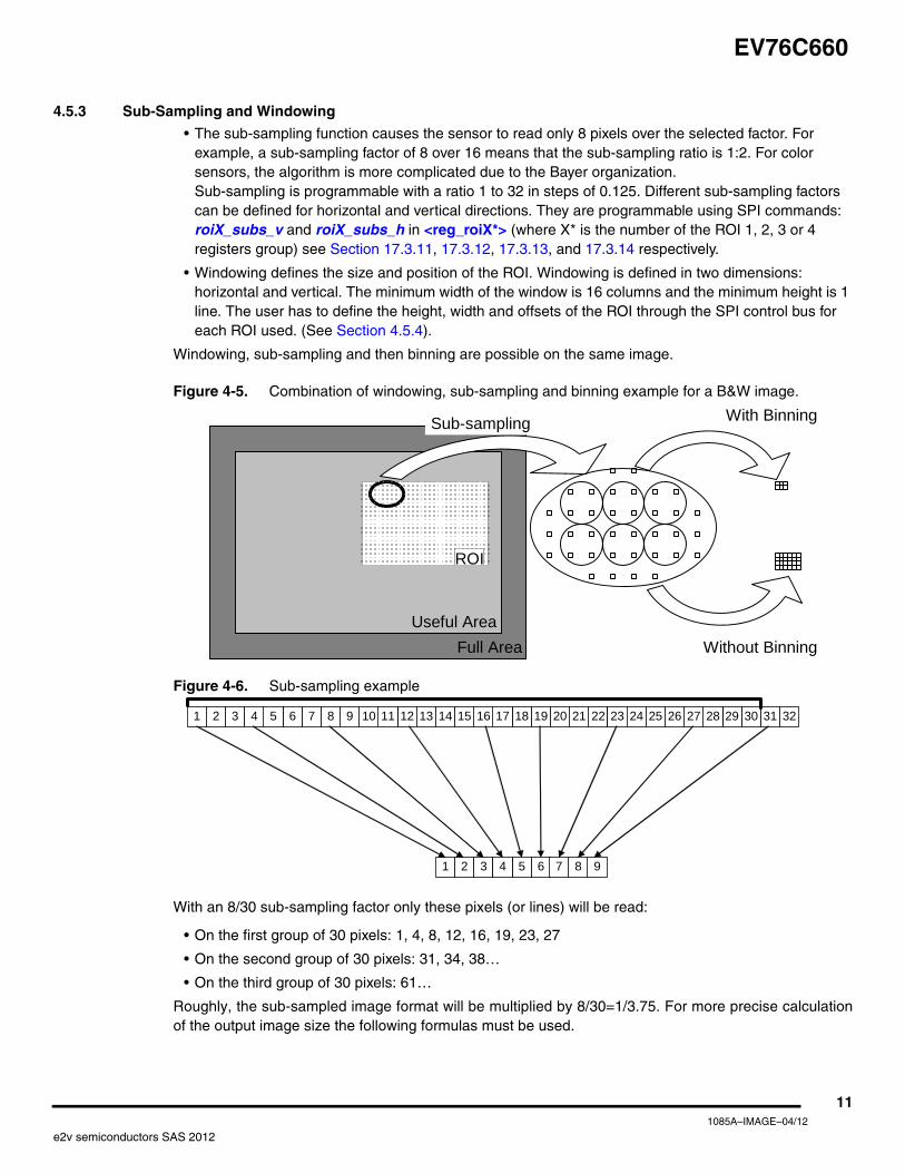
• The sub-sampling function causes the sensor to read only 8 pixels over the selected factor. For example, a sub-sampling factor of 8 over 16 means that the sub-sampling ratio is 1:2. For color sensors, the algorithm is more complicated due to the Bayer organization.Sub-sampling is programmable with a ratio 1 to 32 in steps of 0.125. Different sub-sampling factors can be defined for horizontal and vertical directions. They are programmable using SPI commands: roiX_subs_v and roiX_subs_h in <reg_roiX*> (where X* is the number of the ROI 1, 2, 3 or 4 registers group) see Section 17.3.11, 17.3.12, 17.3.13, and 17.3.14 respectively.
• Windowing defines the size and position of the ROI. Windowing is defined in two dimensions: horizontal and vertical. The minimum width of the window is 16 columns and the minimum height is 1 line. The user has to define the height, width and offsets of the ROI through the SPI control bus for each ROI used. (See Section 4.5.4).
Windowing, sub-sampling and then binning are possible on the same image.
Figure 4-5. Combination of windowing, sub-sampling and binning example for a B&W image.
Figure 4-6. Sub-sampling example
With an 8/30 sub-sampling factor only these pixels (or lines) will be read:
• On the first group of 30 pixels: 1, 4, 8, 12, 16, 19, 23, 27
• On the second group of 30 pixels: 31, 34, 38…
• On the third group of 30 pixels: 61…
Roughly, the sub-sampled image format will be multiplied by 8/30=1/3.75. For more precise calculationof the output image size the following formulas must be used.
Full AreaUseful Area
ROI
Without Binning
With BinningSub-sampling
12 13 14 22212019181716151 2 3 11109 8 7 6 5 4 23 24 25 3231302928 27 26
1 2 3 654 987
111085A–IMAGE–04/12
e2v semiconductors SAS 2012
EV76C660
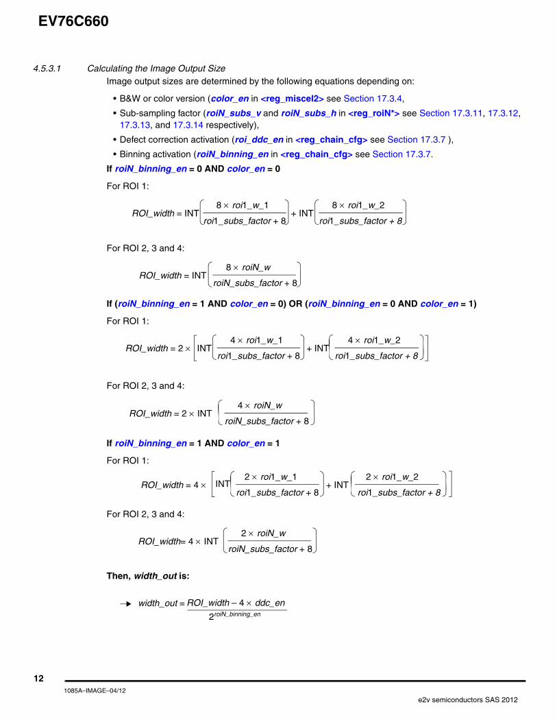
4.5.3.1 Calculating the Image Output SizeImage output sizes are determined by the following equations depending on:
• B&W or color version (color_en in <reg_miscel2> see Section 17.3.4,
• Sub-sampling factor (roiN_subs_v and roiN_subs_h in <reg_roiN*> see Section 17.3.11, 17.3.12, 17.3.13, and 17.3.14 respectively),
• Defect correction activation (roi_ddc_en in <reg_chain_cfg> see Section 17.3.7 ),
• Binning activation (roiN_binning_en in <reg_chain_cfg> see Section 17.3.7.
If roiN_binning_en = 0 AND color_en = 0
For ROI 1:
For ROI 2, 3 and 4:
If (roiN_binning_en = 1 AND color_en = 0) OR (roiN_binning_en = 0 AND color_en = 1)
For ROI 1:
For ROI 2, 3 and 4:
If roiN_binning_en = 1 AND color_en = 1
For ROI 1:
For ROI 2, 3 and 4:
Then, width_out is:
ROI_width = INT8 × roi1_w_1
roi1_subs_factor + 8+ INT
8 × roi1_w_2
roi1_subs_factor + 8
ROI_width = INT8 × roiN_w
roiN_subs_factor + 8
ROI_width = 2 × 4 × roi1_w_1
roi1_subs_factor + 8+ INT
4 × roi1_w_2
roi1_subs_factor + 8INT
ROI_width = 2 × INT4 × roiN_w
roiN_subs_factor + 8
ROI_width = 4 × 2 × roi1_w_1
roi1_subs_factor + 8+ INT
2 × roi1_w_2
roi1_subs_factor + 8INT
ROI_width= 4 × INT2 × roiN_w
roiN_subs_factor + 8
width_out = ROI_width – 4 × ddc_en
2roiN_binning_en
121085A–IMAGE–04/12
e2v semiconductors SAS 2012
EV76C660
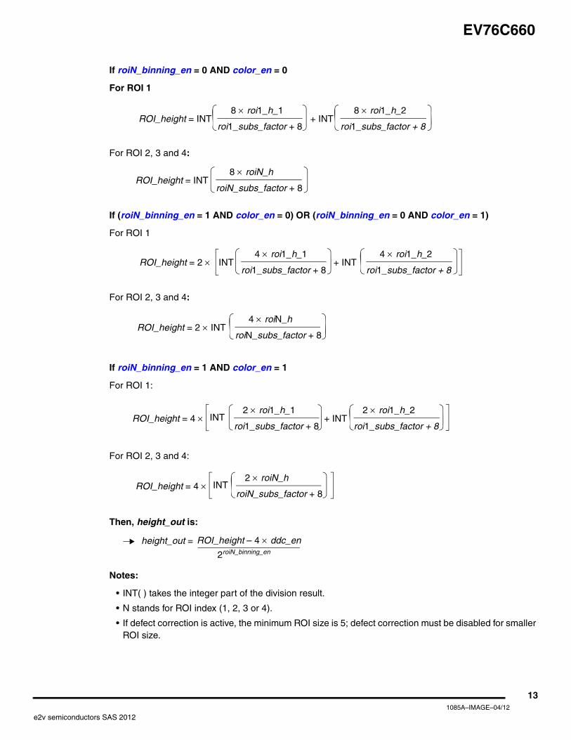
If roiN_binning_en = 0 AND color_en = 0
For ROI 1
For ROI 2, 3 and 4:
If (roiN_binning_en = 1 AND color_en = 0) OR (roiN_binning_en = 0 AND color_en = 1)
For ROI 1
For ROI 2, 3 and 4:
If roiN_binning_en = 1 AND color_en = 1
For ROI 1:
For ROI 2, 3 and 4:
Then, height_out is:
Notes:
• INT( ) takes the integer part of the division result.
• N stands for ROI index (1, 2, 3 or 4).
• If defect correction is active, the minimum ROI size is 5; defect correction must be disabled for smaller ROI size.
ROI_height = INT8 × roi1_h_1
roi1_subs_factor + 8+ INT
8 × roi1_h_2
roi1_subs_factor + 8
ROI_height = INT8 × roiN_h
roiN_subs_factor + 8
ROI_height = 2 × 4 × roi1_h_1
roi1_subs_factor + 8+ INT
4 × roi1_h_2
roi1_subs_factor + 8INT
ROI_height = 2 × 4 × roiN_h
roiN_subs_factor + 8INT
ROI_height = 4 × 2 × roi1_h_1
roi1_subs_factor + 8+ INT
2 × roi1_h_2
roi1_subs_factor + 8INT
ROI_height = 4 × 2 × roiN_h
roiN_subs_factor + 8INT
height_out = ROI_height – 4 × ddc_en
2roiN_binning_en
131085A–IMAGE–04/12
e2v semiconductors SAS 2012
EV76C660
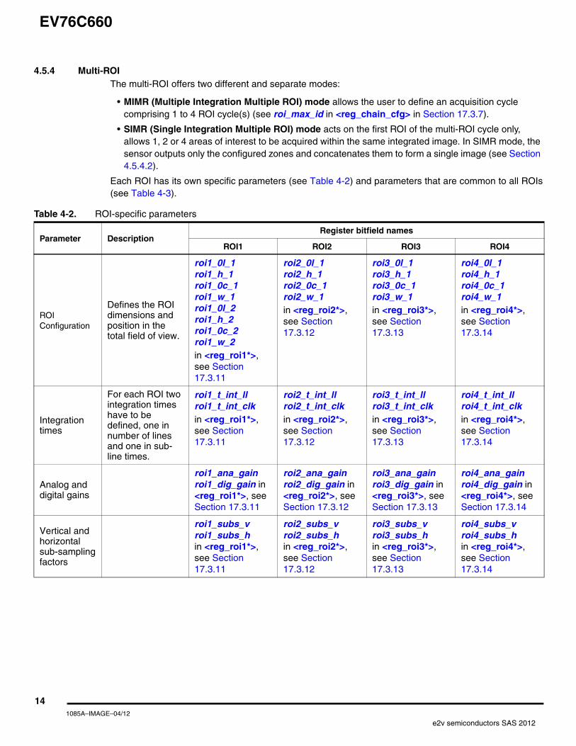
4.5.4 Multi-ROIThe multi-ROI offers two different and separate modes:
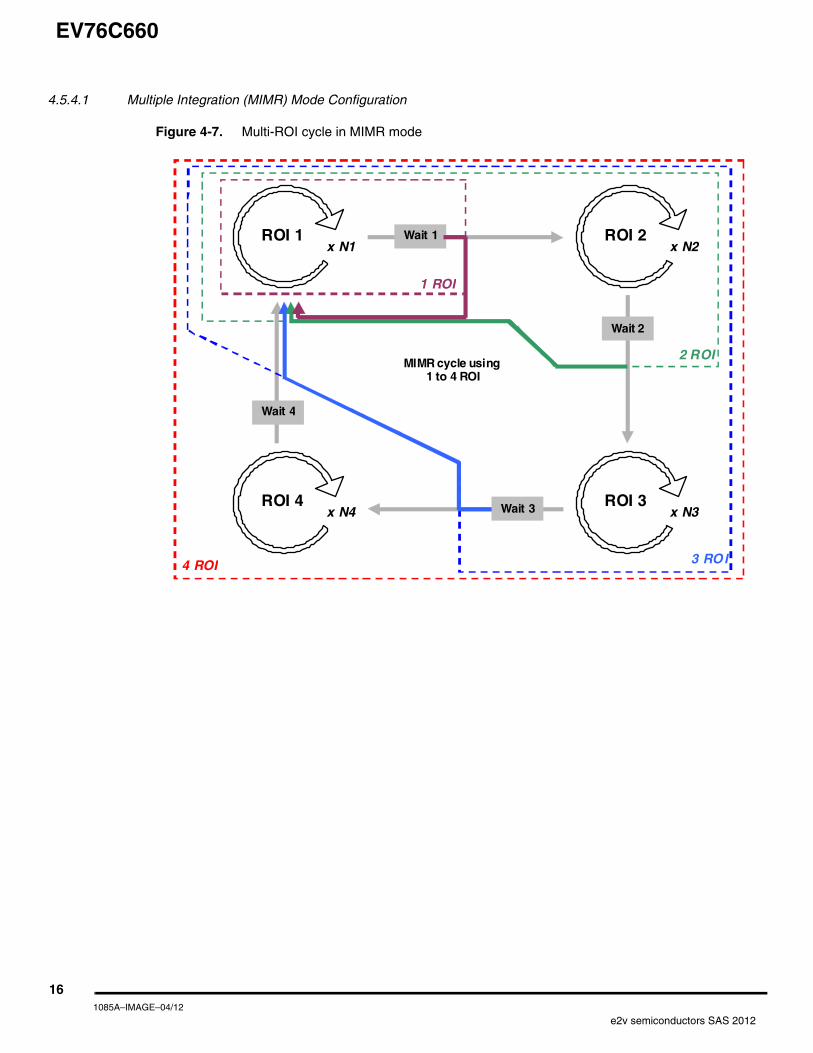
• MIMR (Multiple Integration Multiple ROI) mode allows the user to define an acquisition cycle comprising 1 to 4 ROI cycle(s) (see roi_max_id in <reg_chain_cfg> in Section 17.3.7).
• SIMR (Single Integration Multiple ROI) mode acts on the first ROI of the multi-ROI cycle only, allows 1, 2 or 4 areas of interest to be acquired within the same integrated image. In SIMR mode, the sensor outputs only the configured zones and concatenates them to form a single image (see Section 4.5.4.2).
Each ROI has its own specific parameters (see Table 4-2) and parameters that are common to all ROIs(see Table 4-3).
Table 4-2. ROI-specific parameters
Parameter DescriptionRegister bitfield names
ROI1 ROI2 ROI3 ROI4
ROI Configuration
Defines the ROI dimensions and position in the total field of view.
roi1_0l_1 roi1_h_1 roi1_0c_1 roi1_w_1 roi1_0l_2 roi1_h_2 roi1_0c_2 roi1_w_2in <reg_roi1*>, see Section 17.3.11
roi2_0l_1 roi2_h_1 roi2_0c_1 roi2_w_1in <reg_roi2*>, see Section 17.3.12
roi3_0l_1 roi3_h_1 roi3_0c_1 roi3_w_1in <reg_roi3*>, see Section 17.3.13
roi4_0l_1 roi4_h_1 roi4_0c_1 roi4_w_1 in <reg_roi4*>, see Section 17.3.14
Integration times
For each ROI two integration times have to be defined, one in number of lines and one in sub-line times.
roi1_t_int_ll roi1_t_int_clkin <reg_roi1*>, see Section 17.3.11
roi2_t_int_ll roi2_t_int_clkin <reg_roi2*>, see Section 17.3.12
roi3_t_int_ll roi3_t_int_clkin <reg_roi3*>, see Section 17.3.13
roi4_t_int_ll roi4_t_int_clkin <reg_roi4*>, see Section 17.3.14
Analog and digital gains
roi1_ana_gain roi1_dig_gain in <reg_roi1*>, see Section 17.3.11
roi2_ana_gain roi2_dig_gain in <reg_roi2*>, see Section 17.3.12
roi3_ana_gain roi3_dig_gain in <reg_roi3*>, see Section 17.3.13
roi4_ana_gain roi4_dig_gain in <reg_roi4*>, see Section 17.3.14
Vertical and horizontal sub-sampling factors
roi1_subs_v roi1_subs_h in <reg_roi1*>, see Section 17.3.11
roi2_subs_v roi2_subs_hin <reg_roi2*>, see Section 17.3.12
roi3_subs_v roi3_subs_hin <reg_roi3*>, see Section 17.3.13
roi4_subs_v roi4_subs_h in <reg_roi4*>, see Section 17.3.14
141085A–IMAGE–04/12
e2v semiconductors SAS 2012
EV76C660
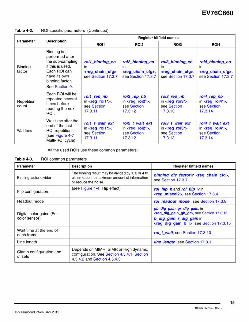
All the used ROIs use these common parameters:
Binning factor
Binning is performed after the sub-sampling if this is used. Each ROI can have its own binning factor.See Section 9.
roi1_binning_en in <reg_chain_cfg>, see Section 17.3.7
roi2_binning_en in <reg_chain_cfg>, see Section 17.3.7
roi3_binning_en in <reg_chain_cfg>, see Section 17.3.7
roi4_binning_en in <reg_chain_cfg>, see Section 17.3.7
Repetition count
Each ROI will be repeated several times before reading the next ROI.
roi1_rep_nb in <reg_roi1*>, see Section 17.3.11
roi2_rep_nb in <reg_roi2*>, see Section 17.3.12
roi3_rep_nb in <reg_roi3*>, see Section 17.3.13
roi4_rep_nb in <reg_roi4*>, see Section 17.3.14
Wait time
Wait time after the end of the last ROI repetition (see Figure 4-7 Multi-ROI cycle).
roi1_t_wait_ext in <reg_roi1*>, see Section 17.3.11
roi2_t_wait_ext in <reg_roi2*>, see Section 17.3.12
roi3_t_wait_ext in <reg_roi3*>, see Section 17.3.13
roi4_t_wait_ext in <reg_roi4*>, see Section 17.3.14
Table 4-2. ROI-specific parameters (Continued)
Parameter DescriptionRegister bitfield names
ROI1 ROI2 ROI3 ROI4
Table 4-3. ROI common parameters
Parameter Description Register bitfield names
Binning factor dividerThe binning result may be divided by 1, 2 or 4 to either keep the maximum amount of information or reduce the noise.
binning_div_factor in <reg_chain_cfg>, see Section 17.3.7
Flip configuration(see Figure 4-4: Flip effect) roi_flip_h and roi_flip_v in
<reg_miscel2>, see Section 17.3.4
Readout mode roi_readout_mode , see Section 17.3.8
Digital color gains (For color sensor)
gb_dig_gain; gr_dig_gain; in <reg_dig_gain_gb_gr>, see Section 17.3.16
b_dig_gain; r_dig_gain in <reg_dig_gain_b_r>, see Section 17.3.15
Wait time at the end of each frame roi_t_wait, see Section 17.3.10
Line length line_length, see Section 17.3.1
Clamp configuration and offsets
Depends on MIMR, SIMR or High dynamic configuration. See Section 4.5.4.1, Section 4.5.4.2 and Section 4.5.4.3
151085A–IMAGE–04/12
e2v semiconductors SAS 2012
EV76C660
4.5.4.1 Multiple Integration (MIMR) Mode Configuration
Figure 4-7. Multi-ROI cycle in MIMR mode
Wait 1
MIMR cycle using 1 to 4 ROI
ROI 1x N1
ROI 2x N2
ROI 3x N3
Wait 2
ROI 4x N4 Wait 3
Wait 4
4 ROI
2 ROI
3 ROI
1 ROI
161085A–IMAGE–04/12
e2v semiconductors SAS 2012
EV76C660
4.5.4.2 Single Integration (SIMR) Mode Configuration
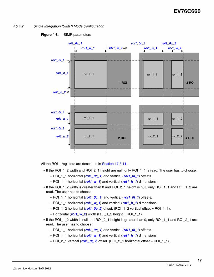
Figure 4-8. SIMR parameters
All the ROI 1 registers are described in Section 17.3.11.
• If the ROI_1_2 width and ROI_2_1 height are null, only ROI_1_1 is read. The user has to choose:
– ROI_1_1 horizontal (roi1_0c_1) and vertical (roi1_0l_1) offsets.
– ROI_1_1 horizontal (roi1_w_1) and vertical (roi1_h_1) dimensions.
• If the ROI_1_2 width is greater than 0 and ROI_2_1 height is null, only ROI_1_1 and ROI_1_2 are read. The user has to choose:
– ROI_1_1 horizontal (roi1_0c_1) and vertical (roi1_0l_1) offsets.
– ROI_1_1 horizontal (roi1_w_1) and vertical (roi1_h_1) dimensions.
– ROI_1_2 horizontal (roi1_0c_2) offset. (ROI_1_2 vertical offset = ROI_1_1).
– Horizontal (roi1_w_2) width (ROI_1_2 height = ROI_1_1).
• If the ROI_1_2 width is null and ROI_2_1 height is greater than 0, only ROI_1_1 and ROI_2_1 are read. The user has to choose:
– ROI_1_1 horizontal (roi1_0c_1) and vertical (roi1_0l_1) offsets.
– ROI_1_1 horizontal (roi1_w_1) and vertical (roi1_h_1) dimensions.
– ROI_2_1 vertical (roi1_0l_2) offset. (ROI_2_1 horizontal offset = ROI_1_1).
4 ROI 2 ROI
2 ROI 1 ROI
roi1_0c_1
roi1_0l_1
roi1_w_1
roi1_h_1
roi1_0c_1 roi1_0c_2
roi1_w_1 roi1_w_2
roi1_0l_1
roi1_0l_2
roi1_h_1
roi1_h_2
roi_1_1 roi_1_1
roi_1_1 roi_1_1
roi_1_2
roi_1_2
roi_2_1 roi_2_1 roi_2_2
roi1_w_2 =0
roi1_h_2=0
171085A–IMAGE–04/12
e2v semiconductors SAS 2012
EV76C660
– ROI_2_1 height (roi1_h_2) (ROI_2_1 width is the same as ROI_1_1).
• If the ROI_1_2 width and ROI_2_1 height are greater than 0, then 4 ROI_1_1, ROI_2_1, ROI_1_2 and ROI_2_2 are read. The user has to choose:
– ROI_1_1 horizontal (roi1_0c_1) and vertical (roi1_0l_1) offsets.
– ROI_1_1 horizontal (roi1_w_1) and vertical (roi1_h_1) dimensions.
– ROI_2_1 ROI_2_2 vertical (roi1_0l_2) offset and (roi1_h_1) height.
– ROI_1_2 horizontal (roi1_0c_2) offset and (roi1_w_2) width.
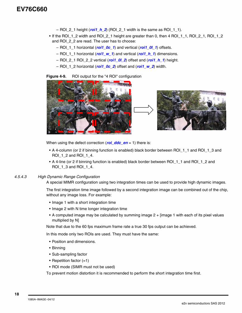
Figure 4-9. ROI output for the "4 ROI" configuration
When using the defect correction (roi_ddc_en = 1) there is:
• A 4-column (or 2 if binning function is enabled) black border between ROI_1_1 and ROI_1_3 and ROI_1_2 and ROI_1_4.
• A 4-line (or 2 if binning function is enabled) black border between ROI_1_1 and ROI_1_2 and ROI_1_3 and ROI_1_4.
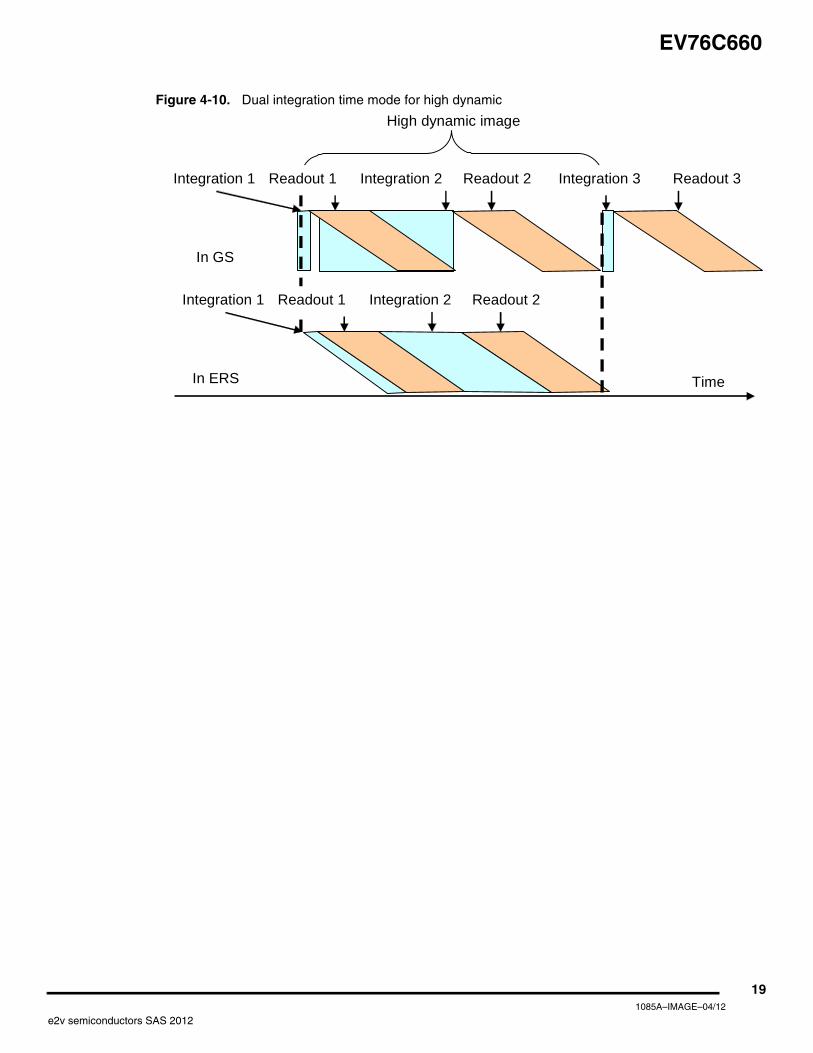
4.5.4.3 High Dynamic Range ConfigurationA special MIMR configuration using two integration times can be used to provide high dynamic images.
The first integration time image followed by a second integration image can be combined out of the chip,without any image loss. For example:
• Image 1 with a short integration time
• Image 2 with N time longer integration time
• A computed image may be calculated by summing image 2 + [image 1 with each of its pixel values multiplied by N]
Note that due to the 60 fps maximum frame rate a true 30 fps output can be achieved.
In this mode only two ROIs are used. They must have the same:
• Position and dimensions.
• Binning
• Sub-sampling factor
• Repetition factor (=1)
• ROI mode (SIMR must not be used)
To prevent motion distortion it is recommended to perform the short integration time first.
181085A–IMAGE–04/12
e2v semiconductors SAS 2012
EV76C660
Figure 4-10. Dual integration time mode for high dynamic
Integration 1 Integration 2 Readout 2 Readout 3
Time
Integration 1 Integration 2 Readout 2
In GS
In ERS
High dynamic image
Readout 1
Readout 1 Integration 3
191085A–IMAGE–04/12
e2v semiconductors SAS 2012
EV76C660
5. 10-Bit ADC
5.1 Analog GainDigital conversion is done by a high speed 10-bit column ADC. All the pixel values of the same line areconverted in parallel.
The analog gain is done by a slope adjustment. There are 8 available values. These values are program-mable via SPI. Each ROI has its own analog gain:
• roi1_ana_gain in <reg_roi1*> for ROI 1 (see Section 17.3.11)
• roi2_ana_gain in <reg_roi2*> for ROI 2 (see Section 17.3.12)
• roi3_ana_gain in <reg_roi3*> for ROI 3 (see Section 17.3.13)
• roi4_ana_gain in <reg_roi4*> for ROI 4 (see Section 17.3.14)
5.2 External Resistor ChoiceThe ADC gain value is set through an external resistor connected between ADC_REF_1 andADC_REF_2 pins. An internal protection against a short circuit between these two pins is included in thedesign.
where K = 1.94 × 10¹², CLK_ADC is in Hertz and REXT is in Ohms.
With a 114 MHz ADC clock, the resistor value is 16.9 kΩ.
5.3 Analog Gain Tolerances
6. Clamp and Offset AdjustmentThe purpose of the automatic black level adjustment function (or clamp) is to cancel:
• The offset due to pixel dark current (offset variable with temperature and integration time).
• The analog chain offset (mainly due to comparator offset).
The black level adjustment is active up to 65 °C with 200 ms integration time.
Black level adjustment can be automatic or manual. This is selected by the clamp_auto_en bit in the<reg_miscel2> register. See Section 17.3.4
In order to compensate possible differences in dark current generation between masked pixels and use-ful pixels, the automatic black level correction works as follows:
REXT = K
CLK_ADC– 80
Table 5-1. ADC gain tolerances
1 1.5 2 3 4 6 8
89.09 59.09 44.18 29.64 22.30 14.90 11.27
Precision 0.5% 1% 1% 1% 1 2%
201085A–IMAGE–04/12
e2v semiconductors SAS 2012
EV76C660
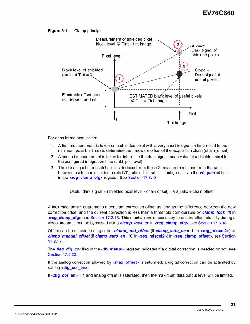
Figure 6-1. Clamp principle
For each frame acquisition:
1. A first measurement is taken on a shielded pixel with a very short integration time (fixed to the minimum possible time) to determine the hardware offset of the acquisition chain (chain_offset).
2. A second measurement is taken to determine the dark signal mean value of a shielded pixel for the configured integration time (shld_pix_level).
3. The dark signal of a useful pixel is deduced from these 2 measurements and from the ratio between useful and shielded pixels (V0_ratio). This ratio is configurable via the v0_gain bit field in the <reg_clamp_cfg> register. See Section 17.3.18.
Useful dark signal = (shielded pixel level - chain offset) × V0_ratio + chain offset
A lock mechanism guarantees a constant correction offset as long as the difference between the newcorrection offset and the current correction is less than a threshold configurable by clamp_lock_th in<reg_clamp_cfg> see Section 17.3.18. This mechanism is necessary to ensure offset stability during avideo stream. It can be bypassed using clamp_lock_en in <reg_clamp_cfg>, see Section 17.3.18.
Offset can be adjusted using either clamp_add_offset (if clamp_auto_en = '1' in <reg_miscel2>) orclamp_manual_offset (if clamp_auto_en = '0' in <reg_miscel2>) in <reg_clamp_offset>, see Section17.3.17.
The flag_dig_cor flag in the <fb_status> register indicates if a digital correction is needed or not, seeSection 17.3.23.
If the analog correction allowed by <max_offset> is saturated, a digital correction can be activated bysetting <dig_cor_en>.
If <dig_cor_en> = 1 and analog offset is saturated, then the maximum data output level will be limited.
Slope= Dark signal of shielded pixels
Slope =Dark signal of useful pixels
Measurement of shielded pixel black level @ Tint = tint image
Black level of shielded pixels at Tint = 0
Tint
Pixel level
Electronic offset does not depend on Tint
ESTIMATED black level of useful pixels @ Tint = Tint image
Tint image 0
1
3
2
211085A–IMAGE–04/12
e2v semiconductors SAS 2012
EV76C660
Digital and analog offsets are output in two feedback bitfields fb_ana_offset and fb_dig_offset in<fb_clamp>, see Section 17.3.22.
Figure 6-2. Clamp algorithm
Yes
No
No
Yes
Yes
No
Yes
No
Compute new_offset
Select current_offset according to ROI id
If |new_offset - current_offset| > clamp_lock_th
Or If clamp_lock_en = 0
If current_offset > max_offset
ana_offset_po = clamp_max_offsetflag_dig_cor = 1
If dig_cor_en = 0
dig_offset = current_offset - ana_offsetdig_offset = 0
current_offset = clamp_manual_offset
current_offset = new_offset
ana_offset = current_offsetflag_dig_cor = 0
If clamp_auto_en = 0
221085A–IMAGE–04/12
e2v semiconductors SAS 2012

EV76C660
7. Digital GainThis block applies one global gain followed by four digital gains (for the Bayer or 2x2 WRGB CFA struc-tures) configurable by 8-bit SPI registers.
In B&W products, only the global gain is used.
To allow good precision with low gains the 8-bits for programming the digital gain are used as follows:
• The 2 MSB are used for precision P
• The 6 LSB are used to control the gain G (from 0 to 63)
• The ROIX digital gains (roiX_dig_gain) follow this rule:
• For P=0 Gain varies from 1 to 1.98 in steps of 0.015
• For P=1 Gain varies from 2 to 3.97 in steps of 0.031
• For P=2 Gain varies from 4 to 7.94 in steps of 0.062
• For P=3 Gain varies from 8 to 15.88 in steps of 0.125
In color products, the four digital gains can be used to balance the four color channels (blue, green blue,green red and red):
• The 2 MSB are used for precision P
• The 6 LSB are used to control the gain G (from 0 to 63)
• The four digital color gains (gb_dig_gain; gr_dig_gain; b_dig_gain; r_dig_gain) follow this rule:
• For P=0 Gain varies from 0.25 to 0.5 in steps of 0.004
• For P=1 Gain varies from 0.5 to 0.99 in steps of 0.008
• For P=2 Gain varies from 1 to 1.98 in steps of 0.016
• For P=3 Gain varies from 2 to 3.97 in steps of 0.0.31
8. Defective Pixel CorrectionA multidirectional 3x3 median filter (with maximal weighting) is implemented and can be enabled by pro-gramming roi_ddc_en in < reg_chain_cfg >. See Section 17.3.7.
This filter is compatible with B&W and color products (Bayer or WRGB). All pixels of the ROI are cor-rected; this correction deletes 2 pixels all around the input picture so the ROI output is reduced by 2pixels in each line and column. See Section 4.5.3.
Gain = 2P × 1 +64G
Gain = 2P –2 × 1 +64G
231085A–IMAGE–04/12
e2v semiconductors SAS 2012
EV76C660
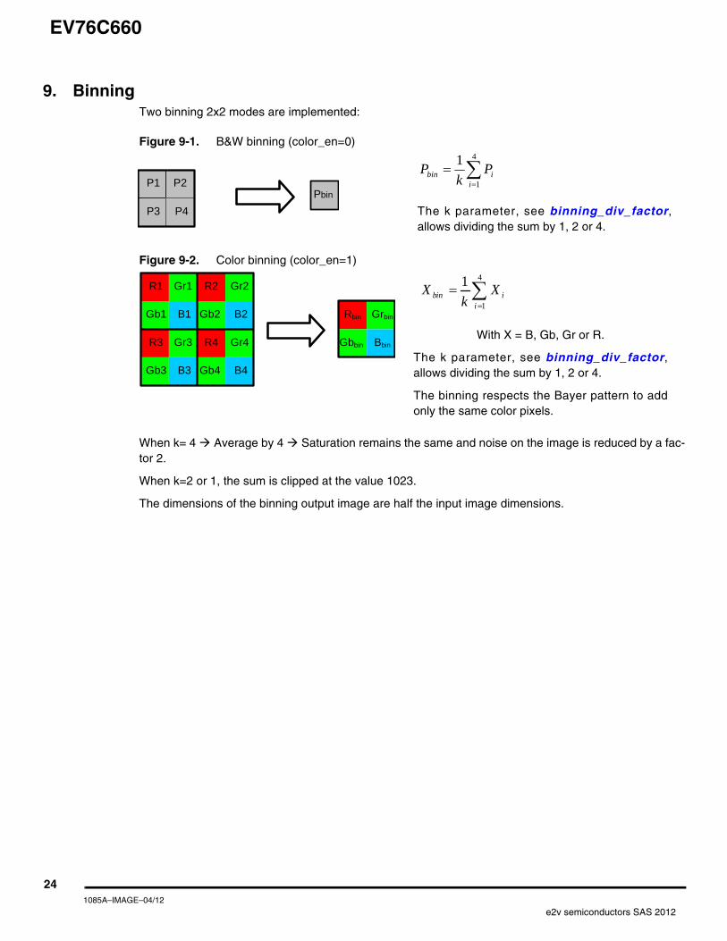
9. BinningTwo binning 2x2 modes are implemented:
Figure 9-1. B&W binning (color_en=0)
Figure 9-2. Color binning (color_en=1)
When k= 4 Average by 4 Saturation remains the same and noise on the image is reduced by a fac-tor 2.
When k=2 or 1, the sum is clipped at the value 1023.
The dimensions of the binning output image are half the input image dimensions.
P1 P2
P4 P3 Pbin
∑=
=4
1
1i
ibin Pk
P
The k parameter, see binning_div_factor,allows dividing the sum by 1, 2 or 4.
R1 R2 Gr1
1Gr2
1Gb2 B1 B2 Gb1
R3 R4 Gr31
Gr41
Gb4 B3 B4 Gb3
Rbin Grbin1
Gbbin BbinWith X = B, Gb, Gr or R.
The k parameter, see binning_div_factor,allows dividing the sum by 1, 2 or 4.
The binning respects the Bayer pattern to addonly the same color pixels.
∑=
=4
1
1i
ibin Xk
X
241085A–IMAGE–04/12
e2v semiconductors SAS 2012
EV76C660
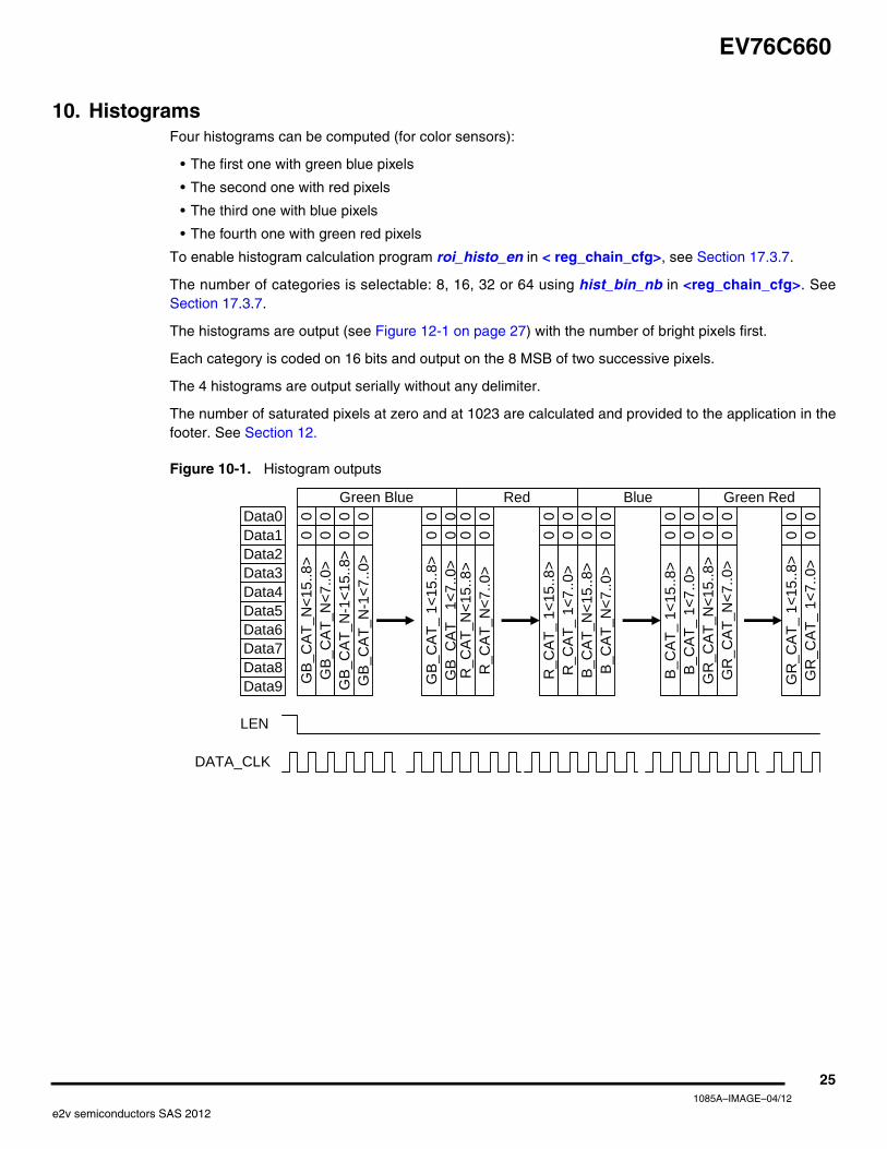
10. HistogramsFour histograms can be computed (for color sensors):
• The first one with green blue pixels
• The second one with red pixels
• The third one with blue pixels
• The fourth one with green red pixels
To enable histogram calculation program roi_histo_en in < reg_chain_cfg>, see Section 17.3.7.
The number of categories is selectable: 8, 16, 32 or 64 using hist_bin_nb in <reg_chain_cfg>. SeeSection 17.3.7.
The histograms are output (see Figure 12-1 on page 27) with the number of bright pixels first.
Each category is coded on 16 bits and output on the 8 MSB of two successive pixels.
The 4 histograms are output serially without any delimiter.
The number of saturated pixels at zero and at 1023 are calculated and provided to the application in thefooter. See Section 12.
Figure 10-1. Histogram outputs
LEN
Data0 Data1 Data2 Data3 Data4 Data5 Data6 Data7 Data8 Data9 G
B_C
AT_N
<15.
.8>
GB
_CAT
_N<7
..0>
GB_
CAT
_N-1
<15.
.8>
GB_
CA
T_N
-1<7
..0>
GB_
CAT
_ 1<
15..8
> G
B_C
AT_
1<7
..0>
0 0
0 0
0 0
0 0
0 0
0 0
Green Blue
R_C
AT_N
<15.
.8>
R_C
AT_
N<7
..0>
R_C
AT_
1<15
..8>
R_C
AT_
1<7.
.0>
0 0
0 0
0 0
0 0
Red
B_C
AT_N
<15.
.8>
B_C
AT_N
<7..0
>
B_C
AT_
1<15
..8>
B_C
AT_
1<7.
.0>
0 0
0 0
0 0
0 0
Blue
GR
_CAT
_N<1
5..8
> G
R_C
AT_N
<7..0
>
GR
_CA
T_ 1
<15.
.8>
GR
_CAT
_ 1<
7..0
>
0 0
0 0
0 0
0 0
Green Red
DATA_CLK
251085A–IMAGE–04/12
e2v semiconductors SAS 2012
EV76C660
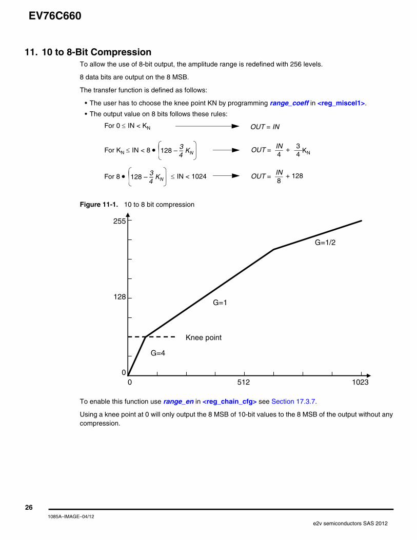
11. 10 to 8-Bit CompressionTo allow the use of 8-bit output, the amplitude range is redefined with 256 levels.
8 data bits are output on the 8 MSB.
The transfer function is defined as follows:
• The user has to choose the knee point KN by programming range_coeff in <reg_miscel1>.
• The output value on 8 bits follows these rules:
Figure 11-1. 10 to 8 bit compression
To enable this function use range_en in <reg_chain_cfg> see Section 17.3.7.
Using a knee point at 0 will only output the 8 MSB of 10-bit values to the 8 MSB of the output without anycompression.
For 0 ≤ IN < KN OUT = IN
For KN ≤ IN < 8 • 128 – – KN34
OUT = IN4
+ 34
KN
For 8 • 128 – – KN34
OUT = IN8
+ 128≤ IN < 1024
0 512 1023
128
0
255
G=4
G=1
G=1/2
Knee point
261085A–IMAGE–04/12
e2v semiconductors SAS 2012
EV76C660
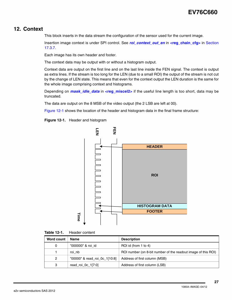
12. ContextThis block inserts in the data stream the configuration of the sensor used for the current image.
Insertion image context is under SPI control. See roi_context_out_en in <reg_chain_cfg> in Section17.3.7.
Each image has its own header and footer.
The context data may be output with or without a histogram output.
Context data are output on the first line and on the last line inside the FEN signal. The context is outputas extra lines. If the stream is too long for the LEN (due to a small ROI) the output of the stream is not cutby the change of LEN state. This means that even for the context output the LEN duration is the same forthe whole image comprising context and histograms.
Depending on mask_idle_data in <reg_miscel2> if the useful line length is too short, data may betruncated.
The data are output on the 8 MSB of the video output (the 2 LSB are left at 00).
Figure 12-1 shows the location of the header and histogram data in the final frame structure:
Figure 12-1. Header and histogram
Table 12-1. Header content
Word count Name Description
0 "000000" & roi_id ROI id (from 1 to 4)
1 roi_nb ROI number (on 8-bit number of the readout image of this ROI)
2 "00000" & read_roi_0c_1[10:8] Address of first column (MSB)
3 read_roi_0c_1[7:0] Address of first column (LSB)
ROI
HEADER
FOOTER HISTOGRAM DATA
FEN
LEN
Time
271085A–IMAGE–04/12
e2v semiconductors SAS 2012
EV76C660
4 "00000" & read_roi_0l_1[10:8] Address of first line (MSB)
5 read_roi_0l_1[7:0] Address of first line (LSB)
6 "00000" & roi_width[10:8] ROI width (MSB)
7 roi_width[7:0] ROI width (LSB)
8 "00000" & roi_height[10:8] ROI Height (MSB)
9 roi_height[7:0] ROI Height (LSB)
10 t_int_ll[15:8] Main ROI integration time in line (MSB)
11 t_int_ll[7:0] Main ROI integration time in line (LSB)
12 "00" & t_int_clk[13:8]MSB of extra ROI integration time in CLK_CTRL × t_int_clk_mult_factor
13 t_int_clk[7:0]LSB of extra ROI integration time in CLK_CTRL × t_int_clk_mult_factor
14 analog_gain ROI analog gain
15 dig_gain_glob ROI Global digital gain
16 dig_gain_b Blue digital gain
17 dig_gain_gb Green blue digital gain
18 dig_gain_gr Green red digital gain
19 dig_gain_r Red digital gain
20 fb_ana_offset Analog offset
21 fb_dig_offset Digital offset
22
'0' (MSB)
fb_flag_dir_cor
fb_error_time_overflow
fb_error_corrupted_video See Section 17.3.23
fb_error_ll_vs_xfer
fb_error_ll_vs_conv
fb_error_t_int_big
fb_error_t_int_small (LSB)
23 t_frame_period_actual[15:8] Frame period (MSB)
24 t_frame_period_actual [7:0] Frame period (LSB)
"00..0" Line is filled with extra 00
Table 12-1. Header content (Continued)
Word count Name Description
281085A–IMAGE–04/12
e2v semiconductors SAS 2012
EV76C660
13. Mux OutThis block multiplexes the different signals to the output: video, context and histograms.
14. Timing Generator and Power ManagementUnder SPI control, the timing generator provides the necessary timing to the sensor. It manages the dif-ferent read modes depending on the global states programmed by the application. It times the reading ofthe matrix to follow the ROI, binning and sub-sampling functions.
Table 12-2. Footer content
Word count Name Description
0
'0'
See sensor status feedback Section 17.3.23.
fb_flag_dir_cor
fb_error_time_overflow
fb_error_corrupted_video
fb_error_ll_vs_xfer
fb_error_ll_vs_conv
fb_error_t_int_big
fb_error_t_int_small
1 low_sat_nb[15:8] Number of pixels at 0 value (MSB)
2 low_sat_nb[7:0] Number of pixels at 0 value (LSB)
3 high_sat_nb[15:8] Number of pixels at 1023 value (MSB)
4 high_sat_nb[7:0] Number of pixels at 1023 value (LSB)
"00..0" Line is filled with extra 00
291085A–IMAGE–04/12
e2v semiconductors SAS 2012
EV76C660
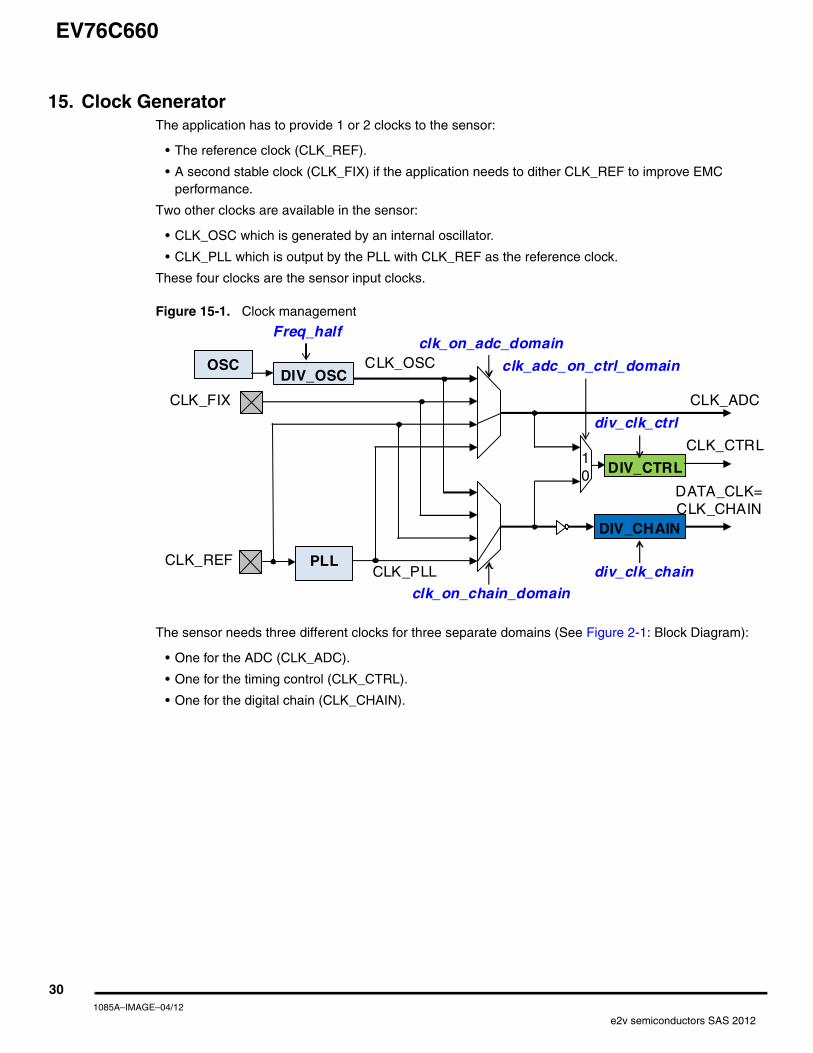
15. Clock GeneratorThe application has to provide 1 or 2 clocks to the sensor:
• The reference clock (CLK_REF).
• A second stable clock (CLK_FIX) if the application needs to dither CLK_REF to improve EMC performance.
Two other clocks are available in the sensor:
• CLK_OSC which is generated by an internal oscillator.
• CLK_PLL which is output by the PLL with CLK_REF as the reference clock.
These four clocks are the sensor input clocks.
Figure 15-1. Clock management
The sensor needs three different clocks for three separate domains (See Figure 2-1: Block Diagram):
• One for the ADC (CLK_ADC).
• One for the timing control (CLK_CTRL).
• One for the digital chain (CLK_CHAIN).
PLL
OSC
DIV_CHAIN
CLK_FIX
1 0
clk_on_chain_domain
DIV_CTRL
clk_on_adc_domain
clk_adc_on_ctrl_domain
CLK_REF
CLK_ADC
CLK_CTRL
CLK_OSC
CLK_PLL
div_clk_ctrl
div_clk_chain
DATA_CLK=CLK_CHAIN
DIV_OSC
Freq_half
301085A–IMAGE–04/12
e2v semiconductors SAS 2012
EV76C660
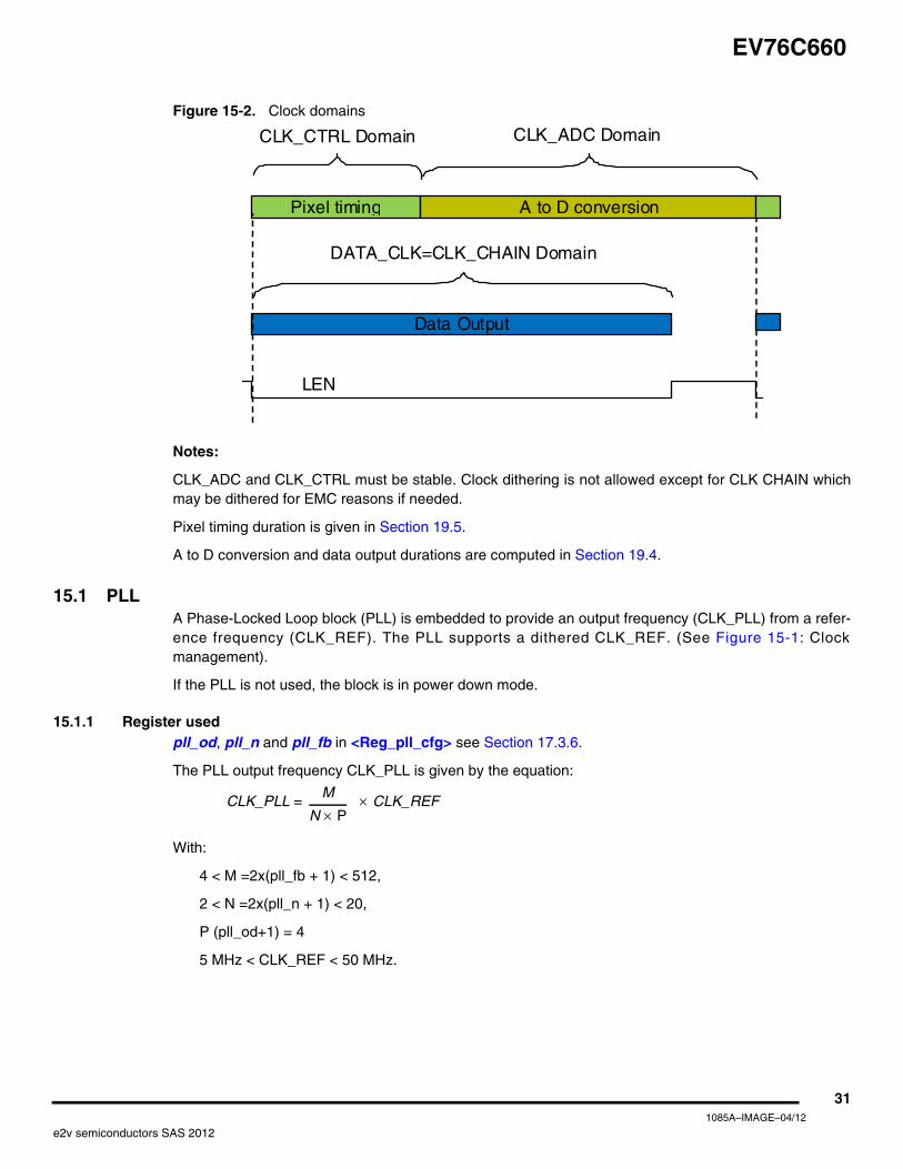
Figure 15-2. Clock domains
Notes:
CLK_ADC and CLK_CTRL must be stable. Clock dithering is not allowed except for CLK CHAIN whichmay be dithered for EMC reasons if needed.
Pixel timing duration is given in Section 19.5.
A to D conversion and data output durations are computed in Section 19.4.
15.1 PLLA Phase-Locked Loop block (PLL) is embedded to provide an output frequency (CLK_PLL) from a refer-ence frequency (CLK_REF). The PLL supports a dithered CLK_REF. (See Figure 15-1: Clockmanagement).
If the PLL is not used, the block is in power down mode.
15.1.1 Register usedpll_od, pll_n and pll_fb in <Reg_pll_cfg> see Section 17.3.6.
The PLL output frequency CLK_PLL is given by the equation:
With:
4 < M =2x(pll_fb + 1) < 512,
2 < N =2x(pll_n + 1) < 20,
P (pll_od+1) = 4
5 MHz < CLK_REF < 50 MHz.
CLK_ADC Domain CLK_CTRL Domain
DATA_CLK=CLK_CHAIN Domain
Pixel timing A to D conversion
Data Output
LEN
CLK_PLL = M
N × P× CLK_REF
311085A–IMAGE–04/12
e2v semiconductors SAS 2012
EV76C660
Figure 15-3. PLL block diagram
15.1.2 Limits and ConditionsThe following conditions and limits must be respected to allow the PLL to operate efficiently:
• 325 MHz < fVCO = CLK_PLL × P < 480 MHz
• 2.5 MHz < fLOOP
• 81.25 MHz < CLK_PLL < 120 MHz
15.1.3 PLL Factor CalculationsFor a given input frequency (CLK_REF) and the desired output frequency (CLK_PLL), follow these stepsto calculate the pll_fb, pll_n and pll_od parameters.
1. Calculation of pll_od:
– pll_od = P-1 = 3
2. Calculation of pll_n:
3. Calculation of pll_fb:
1/N 1/P
1/M
VCOPFD
5
N = 2x(pll_n+1)
8
M = 2x(pll_fb+1)
2
P = f(pll_od)
CLK_PLLCLK_REF
PFD: Phase-Frequency DetectorVCO: Voltage Controlled Oscillator
fVCO
fLOOP
x 2 - 1 IntegerPart CLK_REF
5pll_n =
pll_fb = 2 × RoundedUp (pll_n+1) × CLK_PLL ×(pll +od+1)
CLK_REF-1
321085A–IMAGE–04/12
e2v semiconductors SAS 2012
EV76C660
4. Calculation of the PLL output frequency:
The above formulas can be used to calculate the PLL output frequency (CLK_PLL).
The following table gives the some frequency calculation examples showing the P,N and M parametersettings used to obtain a 114 MHz system frequency with different input reference frequencies. The VCOfrequency is 456 MHz.
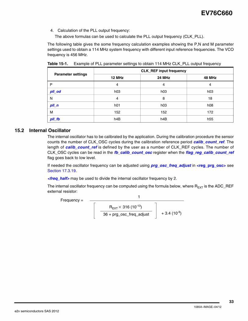
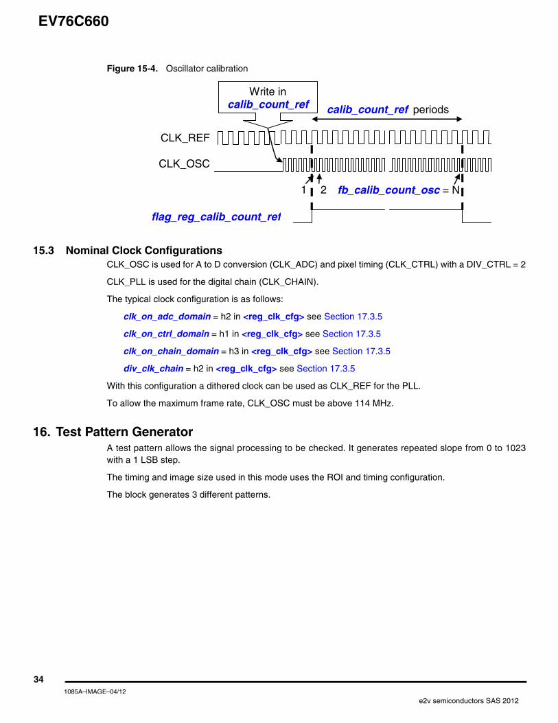
15.2 Internal OscillatorThe internal oscillator has to be calibrated by the application. During the calibration procedure the sensorcounts the number of CLK_OSC cycles during the calibration reference period calib_count_ref. Thelength of calib_count_ref is defined by the user as a number of CLK_REF cycles. The number ofCLK_OSC cycles can be read in the fb_calib_count_osc register when the flag_reg_calib_count_refflag goes back to low level.
If needed the oscillator frequency can be adjusted using prg_osc_freq_adjust in <reg_prg_osc> seeSection 17.3.19.
<freq_half> may be used to divide the internal oscillator frequency by 2.
The internal oscillator frequency can be computed using the formula below, where REXT is the ADC_REFexternal resistor:
Table 15-1. Example of PLL parameter settings to obtain 114 MHz CLK_PLL output frequency
Parameter settingsCLK_REF input frequency
12 MHz 24 MHz 48 MHz
P 4 4 4
pll_od h03 h03 h03
N 4 8 18
pll_n h01 h03 h08
M 152 152 172
pll_fb h4B h4B h55
Frequency =
REXT × 316 (10-13)
+ 3.4 (10-9)
1
36 + prg_osc_freq_adjust
331085A–IMAGE–04/12
e2v semiconductors SAS 2012
EV76C660
Figure 15-4. Oscillator calibration
15.3 Nominal Clock ConfigurationsCLK_OSC is used for A to D conversion (CLK_ADC) and pixel timing (CLK_CTRL) with a DIV_CTRL = 2
CLK_PLL is used for the digital chain (CLK_CHAIN).
The typical clock configuration is as follows:
clk_on_adc_domain = h2 in <reg_clk_cfg> see Section 17.3.5
clk_on_ctrl_domain = h1 in <reg_clk_cfg> see Section 17.3.5
clk_on_chain_domain = h3 in <reg_clk_cfg> see Section 17.3.5
div_clk_chain = h2 in <reg_clk_cfg> see Section 17.3.5
With this configuration a dithered clock can be used as CLK_REF for the PLL.
To allow the maximum frame rate, CLK_OSC must be above 114 MHz.
16. Test Pattern GeneratorA test pattern allows the signal processing to be checked. It generates repeated slope from 0 to 1023with a 1 LSB step.
The timing and image size used in this mode uses the ROI and timing configuration.
The block generates 3 different patterns.
CLK_REF
CLK_OSC
flag_reg_calib_count_ref
calib_count_ref periods
21 fb_calib_count_osc = N
Write in calib_count_ref
341085A–IMAGE–04/12
e2v semiconductors SAS 2012
EV76C660
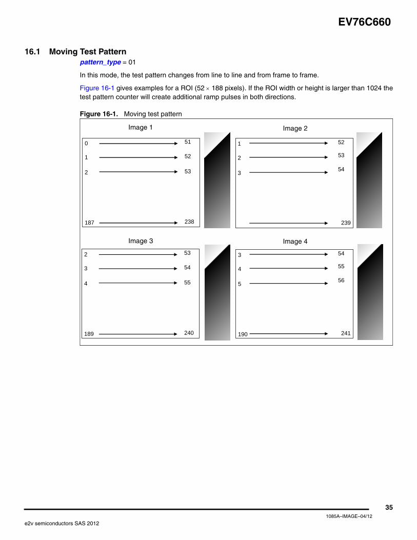
16.1 Moving Test Patternpattern_type = 01
In this mode, the test pattern changes from line to line and from frame to frame.
Figure 16-1 gives examples for a ROI (52 × 188 pixels). If the ROI width or height is larger than 1024 thetest pattern counter will create additional ramp pulses in both directions.
Figure 16-1. Moving test pattern
0 51
1 52
2 53
187 238
1 52
2
3
239
53
54
2 53
3 54
4 55
189 240
3 54
4
5
190 241
55
56
Image 3
Image 2
Image 4
Image 1
351085A–IMAGE–04/12
e2v semiconductors SAS 2012
EV76C660
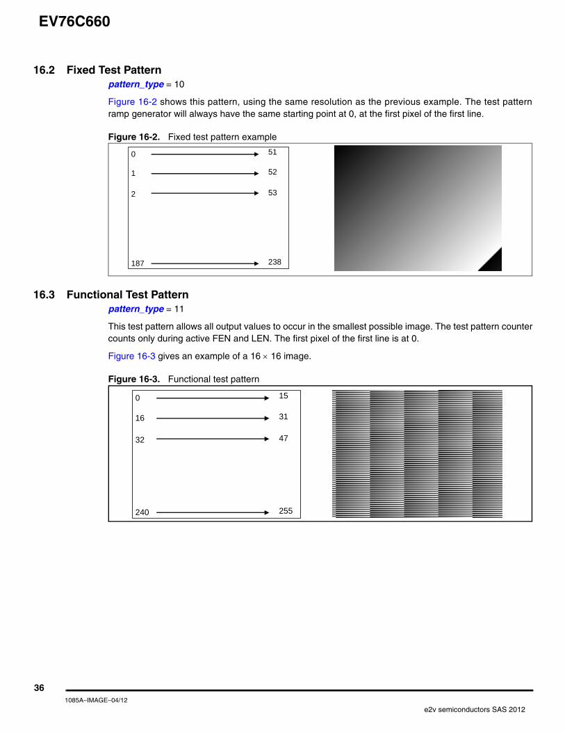
16.2 Fixed Test Patternpattern_type = 10
Figure 16-2 shows this pattern, using the same resolution as the previous example. The test patternramp generator will always have the same starting point at 0, at the first pixel of the first line.
Figure 16-2. Fixed test pattern example
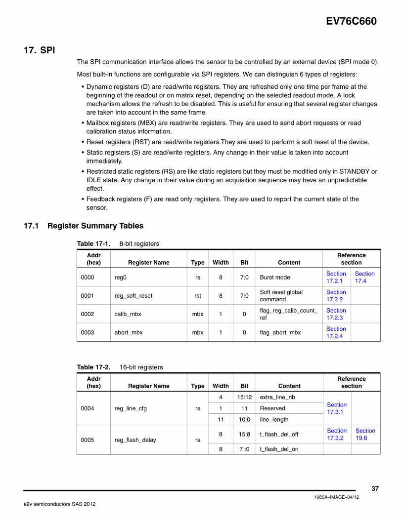
16.3 Functional Test Patternpattern_type = 11
This test pattern allows all output values to occur in the smallest possible image. The test pattern countercounts only during active FEN and LEN. The first pixel of the first line is at 0.
Figure 16-3 gives an example of a 16 × 16 image.
Figure 16-3. Functional test pattern
0 51
1 52
2 53
187 238
0 15
16 31
32 47
240 255
361085A–IMAGE–04/12
e2v semiconductors SAS 2012
EV76C660
17. SPIThe SPI communication interface allows the sensor to be controlled by an external device (SPI mode 0).
Most built-in functions are configurable via SPI registers. We can distinguish 6 types of registers:
• Dynamic registers (D) are read/write registers. They are refreshed only one time per frame at the beginning of the readout or on matrix reset, depending on the selected readout mode. A lock mechanism allows the refresh to be disabled. This is useful for ensuring that several register changes are taken into account in the same frame.
• Mailbox registers (MBX) are read/write registers. They are used to send abort requests or read calibration status information.
• Reset registers (RST) are read/write registers.They are used to perform a soft reset of the device.
• Static registers (S) are read/write registers. Any change in their value is taken into account immediately.
• Restricted static registers (RS) are like static registers but they must be modified only in STANDBY or IDLE state. Any change in their value during an acquisition sequence may have an unpredictable effect.
• Feedback registers (F) are read only registers. They are used to report the current state of the sensor.
17.1 Register Summary Tables
Table 17-1. 8-bit registers
Addr (hex) Register Name Type Width Bit Content
Reference section
0000 reg0 rs 8 7:0 Burst modeSection 17.2.1
Section 17.4
0001 reg_soft_reset rst 8 7:0Soft reset global command
Section 17.2.2
0002 calib_mbx mbx 1 0flag_reg_calib_count_ref
Section 17.2.3
0003 abort_mbx mbx 1 0 flag_abort_mbxSection 17.2.4
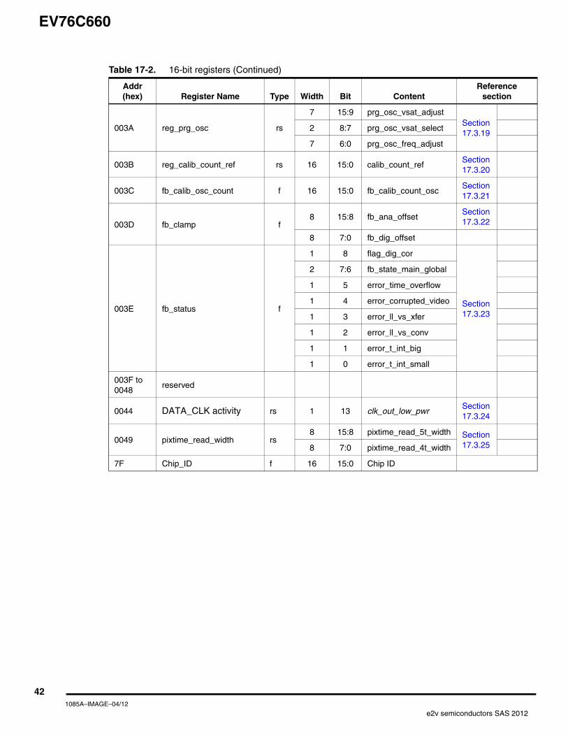
Table 17-2. 16-bit registers
Addr(hex) Register Name Type Width Bit Content
Reference section
0004 reg_line_cfg rs
4 15:12 extra_line_nbSection 17.3.1
1 11 Reserved
11 10:0 line_length
0005 reg_flash_delay rs8 15:8 t_flash_del_off
Section 17.3.2
Section 19.6
8 7 :0 t_flash_del_on
371085A–IMAGE–04/12
e2v semiconductors SAS 2012
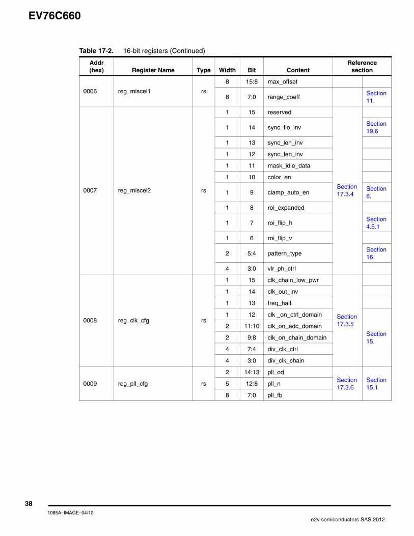
EV76C660
0006 reg_miscel1 rs
8 15:8 max_offset
8 7:0 range_coeffSection 11.
0007 reg_miscel2 rs
1 15 reserved
Section 17.3.4
1 14 sync_flo_invSection 19.6
1 13 sync_len_inv
1 12 sync_fen_inv
1 11 mask_idle_data
1 10 color_en
1 9 clamp_auto_enSection 6.
1 8 roi_expanded
1 7 roi_flip_hSection 4.5.1
1 6 roi_flip_v
2 5:4 pattern_typeSection 16.
4 3:0 vlr_ph_ctrl
0008 reg_clk_cfg rs
1 15 clk_chain_low_pwr
Section 17.3.5
1 14 clk_out_inv
1 13 freq_half
1 12 clk _on_ctrl_domain
Section 15.
2 11:10 clk_on_adc_domain
2 9:8 clk_on_chain_domain
4 7:4 div_clk_ctrl
4 3:0 div_clk_chain
0009 reg_pll_cfg rs
2 14:13 pll_odSection 17.3.6
Section 15.1
5 12:8 pll_n
8 7:0 pll_fb
Table 17-2. 16-bit registers (Continued)
Addr(hex) Register Name Type Width Bit Content
Reference section
381085A–IMAGE–04/12
e2v semiconductors SAS 2012
EV76C660
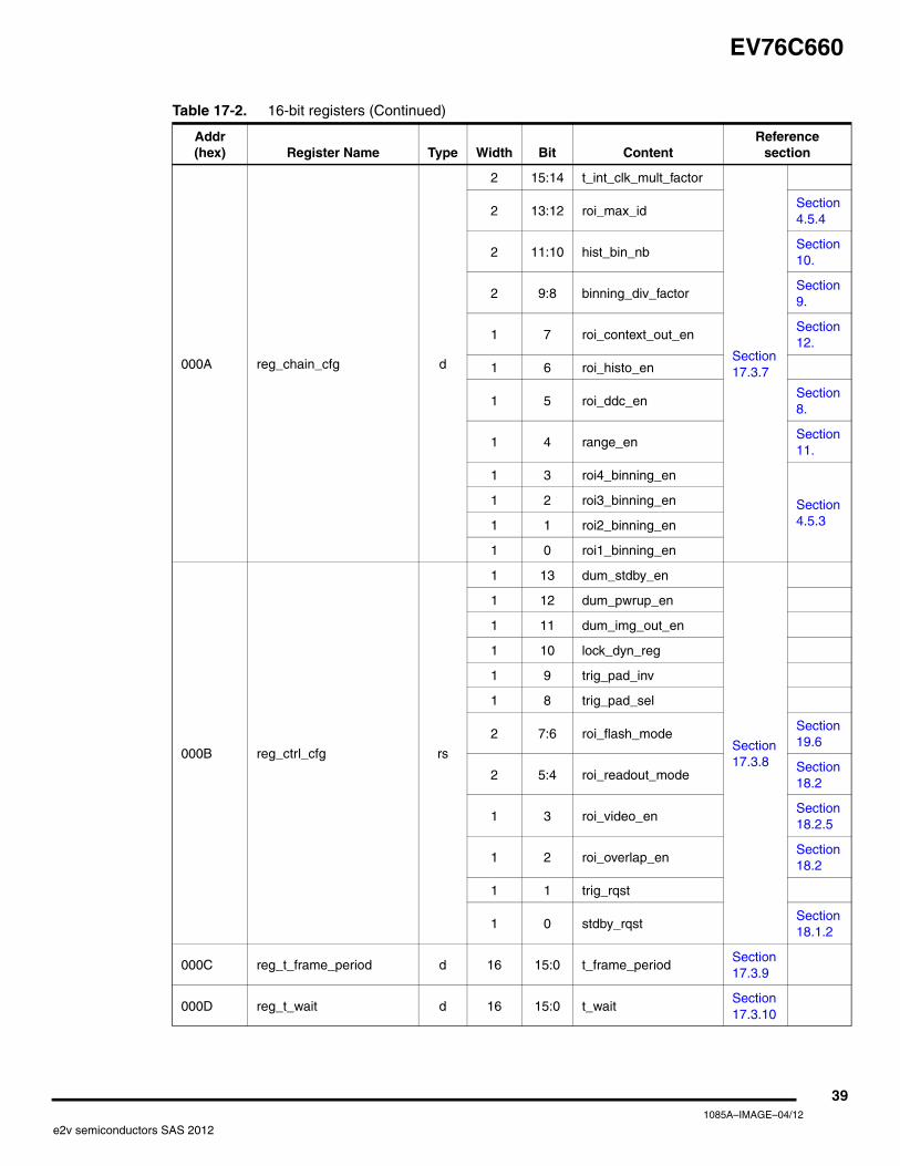
000A reg_chain_cfg d
2 15:14 t_int_clk_mult_factor
Section 17.3.7
2 13:12 roi_max_idSection 4.5.4
2 11:10 hist_bin_nbSection 10.
2 9:8 binning_div_factorSection 9.
1 7 roi_context_out_enSection 12.
1 6 roi_histo_en
1 5 roi_ddc_enSection 8.
1 4 range_enSection 11.
1 3 roi4_binning_en
Section 4.5.3
1 2 roi3_binning_en
1 1 roi2_binning_en
1 0 roi1_binning_en
000B reg_ctrl_cfg rs
1 13 dum_stdby_en
Section 17.3.8
1 12 dum_pwrup_en
1 11 dum_img_out_en
1 10 lock_dyn_reg
1 9 trig_pad_inv
1 8 trig_pad_sel
2 7:6 roi_flash_modeSection 19.6
2 5:4 roi_readout_modeSection 18.2
1 3 roi_video_enSection 18.2.5
1 2 roi_overlap_enSection 18.2
1 1 trig_rqst
1 0 stdby_rqstSection 18.1.2
000C reg_t_frame_period d 16 15:0 t_frame_periodSection 17.3.9
000D reg_t_wait d 16 15:0 t_waitSection 17.3.10
Table 17-2. 16-bit registers (Continued)
Addr(hex) Register Name Type Width Bit Content
Reference section
391085A–IMAGE–04/12
e2v semiconductors SAS 2012
EV76C660
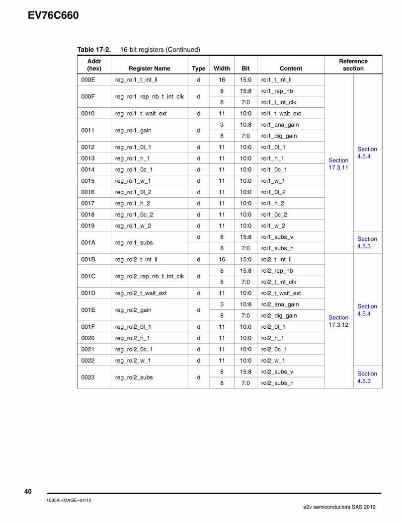
000E reg_roi1_t_int_ll d 16 15:0 roi1_t_int_ll
Section 17.3.11
Section 4.5.4
000F reg_roi1_rep_nb_t_int_clk d8 15:8 roi1_rep_nb
8 7:0 roi1_t_int_clk
0010 reg_roi1_t_wait_ext d 11 10:0 roi1_t_wait_ext
0011 reg_roi1_gain d3 10:8 roi1_ana_gain
8 7:0 roi1_dig_gain
0012 reg_roi1_0l_1 d 11 10:0 roi1_0l_1
0013 reg_roi1_h_1 d 11 10:0 roi1_h_1
0014 reg_roi1_0c_1 d 11 10:0 roi1_0c_1
0015 reg_roi1_w_1 d 11 10:0 roi1_w_1
0016 reg_roi1_0l_2 d 11 10:0 roi1_0l_2
0017 reg_roi1_h_2 d 11 10:0 roi1_h_2
0018 reg_roi1_0c_2 d 11 10:0 roi1_0c_2
0019 reg_roi1_w_2 d 11 10:0 roi1_w_2
001A reg_roi1_subsd 8 15:8 roi1_subs_v Section
4.5.38 7:0 roi1_subs_h
001B reg_roi2_t_int_ll d 16 15:0 roi2_t_int_ll
Section 17.3.12
Section 4.5.4
001C reg_roi2_rep_nb_t_int_clk d8 15:8 roi2_rep_nb
8 7:0 roi2_t_int_clk
001D reg_roi2_t_wait_ext d 11 10:0 roi2_t_wait_ext
001E reg_roi2_gain d3 10:8 roi2_ana_gain
8 7:0 roi2_dig_gain
001F reg_roi2_0l_1 d 11 10:0 roi2_0l_1
0020 reg_roi2_h_1 d 11 10:0 roi2_h_1
0021 reg_roi2_0c_1 d 11 10:0 roi2_0c_1
0022 reg_roi2_w_1 d 11 10:0 roi2_w_1
0023 reg_roi2_subs d8 15:8 roi2_subs_v Section
4.5.38 7:0 roi2_subs_h
Table 17-2. 16-bit registers (Continued)
Addr(hex) Register Name Type Width Bit Content
Reference section
401085A–IMAGE–04/12
e2v semiconductors SAS 2012
EV76C660
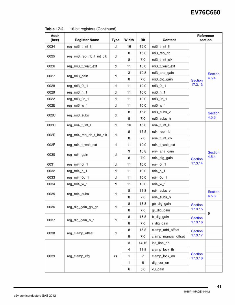
0024 reg_roi3_t_int_ll d 16 15:0 roi3_t_int_ll
Section 17.3.13
Section 4.5.4
0025 reg_roi3_rep_nb_t_int_clk d8 15:8 roi3_rep_nb
8 7:0 roi3_t_int_clk
0026 reg_roi3_t_wait_ext d 11 10:0 roi3_t_wait_ext
0027 reg_roi3_gain d3 10:8 roi3_ana_gain
8 7:0 roi3_dig_gain
0028 reg_roi3_0l_1 d 11 10:0 roi3_0l_1
0029 reg_roi3_h_1 d 11 10:0 roi3_h_1
002A reg_roi3_0c_1 d 11 10:0 roi3_0c_1
002B reg_roi3_w_1 d 11 10:0 roi3_w_1
002C reg_roi3_subs d8 15:8 roi3_subs_v Section
4.5.38 7:0 roi3_subs_h
002D reg_roi4_t_int_ll d 16 15:0 roi4_t_int_ll
Section 17.3.14
Section 4.5.4
002E reg_roi4_rep_nb_t_int_clk d8 15:8 roi4_rep_nb
8 7:0 roi4_t_int_clk
002F reg_roi4_t_wait_ext d 11 10:0 roi4_t_wait_ext
0030 reg_roi4_gain d3 10:8 roi4_ana_gain
8 7:0 roi4_dig_gain
0031 reg_roi4_0l_1 d 11 10:0 roi4_0l_1
0032 reg_roi4_h_1 d 11 10:0 roi4_h_1
0033 reg_roi4_0c_1 d 11 10:0 roi4_0c_1
0034 reg_roi4_w_1 d 11 10:0 roi4_w_1
0035 reg_roi4_subs d8 15:8 roi4_subs_v Section
4.5.38 7:0 roi4_subs_h
0036 reg_dig_gain_gb_gr d8 15:8 gb_dig_gain Section
17.3.159
8 7:0 gr_dig_gain
0037 reg_dig_gain_b_r d8 15:8 b_dig_gain Section
17.3.168 7:0 r_dig_gain
0038 reg_clamp_offset d8 15:8 clamp_add_offset Section
17.3.178 7:0 clamp_manual_offset
0039 reg_clamp_cfg rs
3 14:12 init_line_nb
Section 17.3.18
4 11:8 clamp_lock_th
1 7 clamp_lock_en
1 6 dig_cor_en
6 5:0 v0_gain
Table 17-2. 16-bit registers (Continued)
Addr(hex) Register Name Type Width Bit Content
Reference section
411085A–IMAGE–04/12
e2v semiconductors SAS 2012
EV76C660
003A reg_prg_osc rs
7 15:9 prg_osc_vsat_adjustSection 17.3.19
2 8:7 prg_osc_vsat_select
7 6:0 prg_osc_freq_adjust
003B reg_calib_count_ref rs 16 15:0 calib_count_refSection 17.3.20
003C fb_calib_osc_count f 16 15:0 fb_calib_count_oscSection 17.3.21
003D fb_clamp f8 15:8 fb_ana_offset
Section 17.3.22
8 7:0 fb_dig_offset
003E fb_status f
1 8 flag_dig_cor
Section 17.3.23
2 7:6 fb_state_main_global
1 5 error_time_overflow
1 4 error_corrupted_video
1 3 error_ll_vs_xfer
1 2 error_ll_vs_conv
1 1 error_t_int_big
1 0 error_t_int_small
003F to 0048
reserved
0044 DATA_CLK activity rs 1 13 clk_out_low_pwrSection 17.3.24
0049 pixtime_read_width rs8 15:8 pixtime_read_5t_width Section
17.3.258 7:0 pixtime_read_4t_width
7F Chip_ID f 16 15:0 Chip ID
Table 17-2. 16-bit registers (Continued)
Addr(hex) Register Name Type Width Bit Content
Reference section
421085A–IMAGE–04/12
e2v semiconductors SAS 2012
EV76C660
17.2 8-Bit Register Descriptions
17.2.1 Register 0
17.2.2 Soft Reset Register
Name reg0
Address h00
Type Restricted static
Default h01
Default Value Bitfield name Description
0000 0001 reg0_0[7:0]
Master clock divider:
0 Normal mode active (no burst)1 Burst mode active
Name reg_soft_reset
Address h01
Type Reset
Default h00
Default Value Bitfield name Description
0000 0000 soft_reset[7:0]Soft reset
Writing or reading in SPI address h01 resets the whole chip, except the SPI state machine
431085A–IMAGE–04/12
e2v semiconductors SAS 2012
EV76C660
17.2.3 Calibration Mailbox
17.2.4 Abort Mailbox
Name calib_mbx
Address h02
Type Mailbox
Default h00
Default Value Bitfield name Description
0000 0000 flag_reg_calib_count_ref
Oscillator calibration status
0 Calibration sequence has ended (or not requested)1 Request was recorded. Calibration is ongoing. See reg_calib_count_ref in Section 17.3.20.
Name abort_mbx
Address h03
Type Mailbox
Default h00
Default Value Bitfield name Description
0000 0000 flag_abort_mbx
Abort request / Abort statusA write access to flag_abort_mbx generates an abort request. A read access returns the following status.0 Abort has ended (or not requested)
1 Request was recorded. Current sequence should stop within one line duration. The abort action is requested by a single write to the flag_abort_mbx register itself.
441085A–IMAGE–04/12
e2v semiconductors SAS 2012
EV76C660
17.3 16-Bit Register Descriptions
17.3.1 Line Configuration
Name reg_line_cfg
Address h04
Type Restricted static
Default h8070
Default Value Bitfield name Description
1000 ---- ---- ---- extra_line_nb[15:12]
Number of extra lines
Defines the number of extra lines added after ROI readout
Min = 0 1 line added
Default = h8 9 lines addedMax = hF d16 lines added
See Section 19.2.2.
---- 0--- ---- ---- reserved
---- -000 0111 0000 line_length[10:0]
Line lengthDefines the line length specified in CLK_CTRL cycles multiplied by 8 (timing examples below with CLK_CTRL = 57 MHz). Section 19.4 - Line length calculation.
Min = 0
Default = h70 15.72 µsMax = h7FF 287 µs
451085A–IMAGE–04/12
e2v semiconductors SAS 2012
EV76C660
17.3.2 Flash Delay
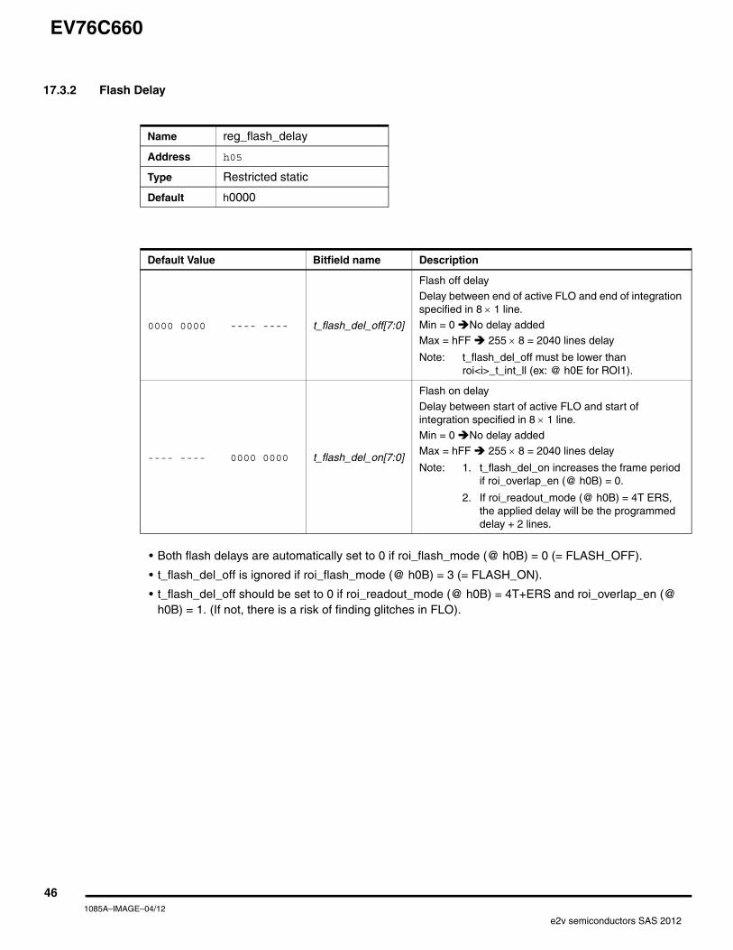
• Both flash delays are automatically set to 0 if roi_flash_mode (@ h0B) = 0 (= FLASH_OFF).
• t_flash_del_off is ignored if roi_flash_mode (@ h0B) = 3 (= FLASH_ON).
• t_flash_del_off should be set to 0 if roi_readout_mode (@ h0B) = 4T+ERS and roi_overlap_en (@ h0B) = 1. (If not, there is a risk of finding glitches in FLO).
Name reg_flash_delay
Address h05
Type Restricted static
Default h0000
Default Value Bitfield name Description
0000 0000 ---- ---- t_flash_del_off[7:0]
Flash off delay
Delay between end of active FLO and end of integration specified in 8 × 1 line.
Min = 0 No delay addedMax = hFF 255 × 8 = 2040 lines delay
Note: t_flash_del_off must be lower than roi<i>_t_int_ll (ex: @ h0E for ROI1).
---- ---- 0000 0000 t_flash_del_on[7:0]
Flash on delay
Delay between start of active FLO and start of integration specified in 8 × 1 line.
Min = 0 No delay added
Max = hFF 255 × 8 = 2040 lines delay
Note: 1. t_flash_del_on increases the frame period if roi_overlap_en (@ h0B) = 0.
2. If roi_readout_mode (@ h0B) = 4T ERS, the applied delay will be the programmed delay + 2 lines.
461085A–IMAGE–04/12
e2v semiconductors SAS 2012
EV76C660
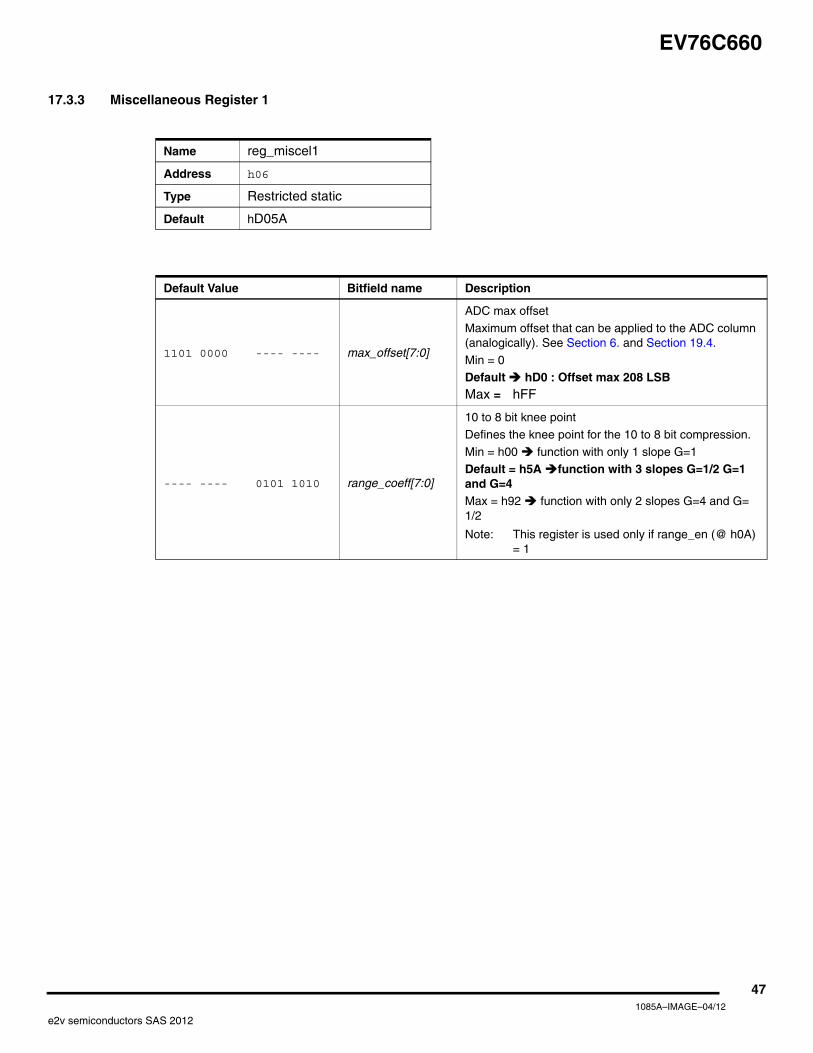
17.3.3 Miscellaneous Register 1
Name reg_miscel1
Address h06
Type Restricted static
Default hD05A
Default Value Bitfield name Description
1101 0000 ---- ---- max_offset[7:0]
ADC max offset
Maximum offset that can be applied to the ADC column (analogically). See Section 6. and Section 19.4.
Min = 0 Default hD0 : Offset max 208 LSB Max = hFF
---- ---- 0101 1010 range_coeff[7:0]
10 to 8 bit knee point
Defines the knee point for the 10 to 8 bit compression.
Min = h00 function with only 1 slope G=1Default = h5A function with 3 slopes G=1/2 G=1 and G=4Max = h92 function with only 2 slopes G=4 and G= 1/2
Note: This register is used only if range_en (@ h0A) = 1
471085A–IMAGE–04/12
e2v semiconductors SAS 2012
EV76C660
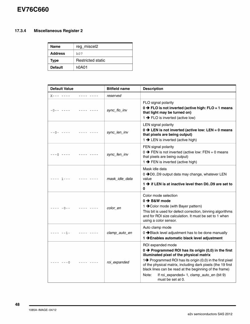
17.3.4 Miscellaneous Register 2
Name reg_miscel2
Address h07
Type Restricted static
Default h0A01
Default Value Bitfield name Description
X--- ---- ---- ---- reserved
-0-- ---- ---- ---- sync_flo_inv
FLO signal polarity
0 FLO is not inverted (active high: FLO = 1 means that light may be turned on)1 FLO is inverted (active low)
--0- ---- ---- ---- sync_len_inv
LEN signal polarity
0 LEN is not inverted (active low: LEN = 0 means that pixels are being output)1 LEN is inverted (active high)
---0 ---- ---- ---- sync_fen_inv
FEN signal polarity
0 FEN is not inverted (active low: FEN = 0 means that pixels are being output)
1 FEN is inverted (active high)
---- 1--- ---- ---- mask_idle_data
Mask idle data
0 D0..D9 output data may change, whatever LEN value
1 if LEN is at inactive level then D0..D9 are set to 0
---- -0-- ---- ---- color_en
Color mode selection0 B&W mode 1 Color mode (with Bayer pattern)
This bit is used for defect correction, binning algorithms and for ROI size calculation. It must be set to 1 when using a color sensor.
---- --1- ---- ---- clamp_auto_enAuto clamp mode0 Black level adjustment has to be done manually
1 Enables automatic black level adjustment
---- ---0 ---- ---- roi_expanded
ROI expanded mode
0 Programmed ROI has its origin (0,0) in the first illuminated pixel of the physical matrix1 Programmed ROI has its origin (0,0) in the first pixel of the physical matrix, including dark pixels (the 19 first black lines can be read at the beginning of the frame)
Note: If roi_expanded= 1, clamp_auto_en (bit 9) must be set at 0.
481085A–IMAGE–04/12
e2v semiconductors SAS 2012
EV76C660
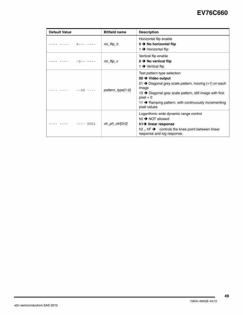
---- ---- 0--- ---- roi_flip_h
Horizontal flip enable
0 No horizontal flip1 Horizontal flip
---- ---- -0-- ---- roi_flip_v
Vertical flip enable
0 No vertical flip1 Vertical flip
---- ---- --00 ---- pattern_type[1:0]
Test pattern type selection00 Video output01 Diagonal grey scale pattern, moving (+1) on each image
10 Diagonal grey scale pattern, still image with first pixel = 0
11 Ramping pattern, with continuously incrementing pixel values
---- ---- ---- 0001 vlr_ph_ctrl[3:0]
Logarithmic wide dynamic range controlh0 NOT allowed
h1 linear responseh2 .. hF controls the knee point between linear response and log response.
Default Value Bitfield name Description
491085A–IMAGE–04/12
e2v semiconductors SAS 2012
EV76C660
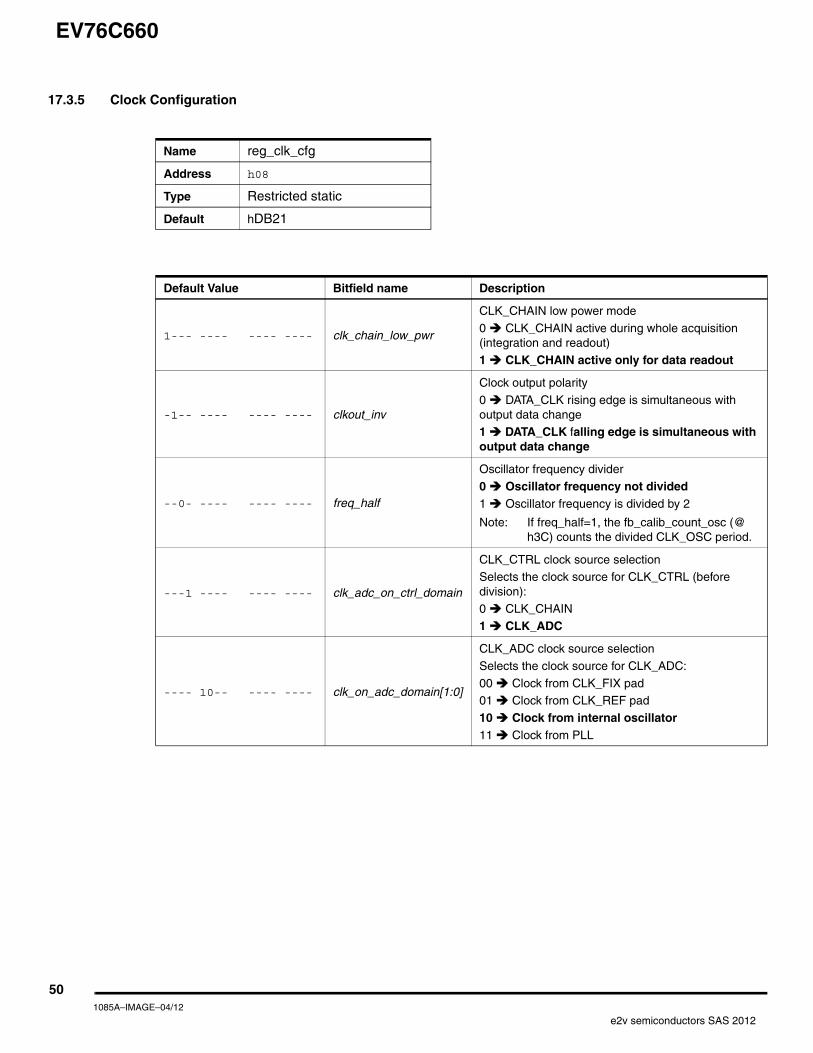
17.3.5 Clock Configuration
Name reg_clk_cfg
Address h08
Type Restricted static
Default hDB21
Default Value Bitfield name Description
1--- ---- ---- ---- clk_chain_low_pwr
CLK_CHAIN low power mode
0 CLK_CHAIN active during whole acquisition (integration and readout)
1 CLK_CHAIN active only for data readout
-1-- ---- ---- ---- clkout_inv
Clock output polarity
0 DATA_CLK rising edge is simultaneous with output data change
1 DATA_CLK falling edge is simultaneous with output data change
--0- ---- ---- ---- freq_half
Oscillator frequency divider
0 Oscillator frequency not divided 1 Oscillator frequency is divided by 2
Note: If freq_half=1, the fb_calib_count_osc (@ h3C) counts the divided CLK_OSC period.
---1 ---- ---- ---- clk_adc_on_ctrl_domain
CLK_CTRL clock source selectionSelects the clock source for CLK_CTRL (before division):0 CLK_CHAIN
1 CLK_ADC
---- 10-- ---- ---- clk_on_adc_domain[1:0]
CLK_ADC clock source selection
Selects the clock source for CLK_ADC:
00 Clock from CLK_FIX pad01 Clock from CLK_REF pad
10 Clock from internal oscillator11 Clock from PLL
501085A–IMAGE–04/12
e2v semiconductors SAS 2012
EV76C660
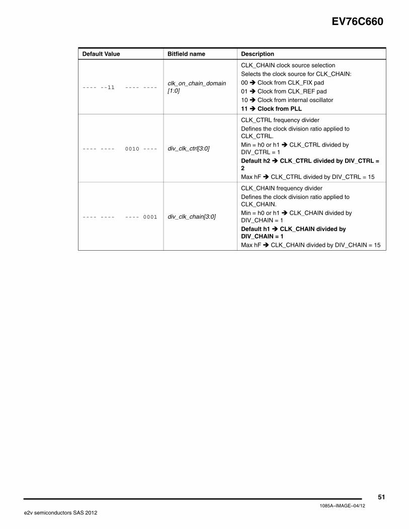
---- --11 ---- ----clk_on_chain_domain [1:0]
CLK_CHAIN clock source selection
Selects the clock source for CLK_CHAIN:00 Clock from CLK_FIX pad
01 Clock from CLK_REF pad
10 Clock from internal oscillator
11 Clock from PLL
---- ---- 0010 ---- div_clk_ctrl[3:0]
CLK_CTRL frequency divider
Defines the clock division ratio applied to CLK_CTRL.
Min = h0 or h1 CLK_CTRL divided by DIV_CTRL = 1
Default h2 CLK_CTRL divided by DIV_CTRL = 2Max hF CLK_CTRL divided by DIV_CTRL = 15
---- ---- ---- 0001 div_clk_chain[3:0]
CLK_CHAIN frequency divider
Defines the clock division ratio applied to CLK_CHAIN.
Min = h0 or h1 CLK_CHAIN divided by DIV_CHAIN = 1
Default h1 CLK_CHAIN divided by DIV_CHAIN = 1Max hF CLK_CHAIN divided by DIV_CHAIN = 15
Default Value Bitfield name Description
511085A–IMAGE–04/12
e2v semiconductors SAS 2012
EV76C660
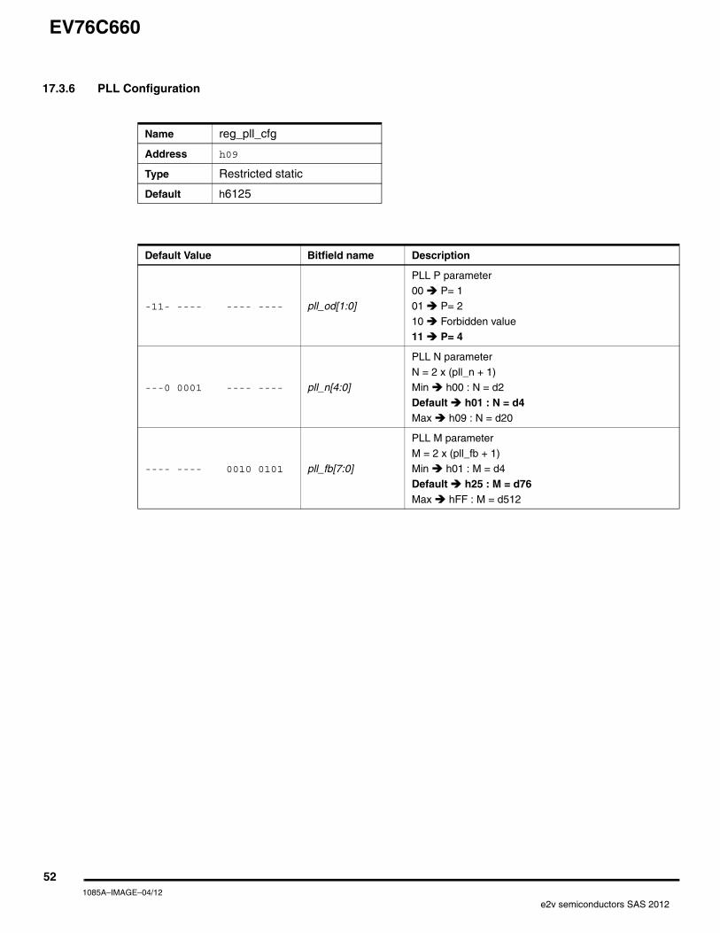
17.3.6 PLL Configuration
Name reg_pll_cfg
Address h09
Type Restricted static
Default h6125
Default Value Bitfield name Description
-11- ---- ---- ---- pll_od[1:0]
PLL P parameter
00 P= 101 P= 2
10 Forbidden value
11 P= 4
---0 0001 ---- ---- pll_n[4:0]
PLL N parameter
N = 2 x (pll_n + 1)Min h00 : N = d2
Default h01 : N = d4Max h09 : N = d20
---- ---- 0010 0101 pll_fb[7:0]
PLL M parameter
M = 2 x (pll_fb + 1)Min h01 : M = d4
Default h25 : M = d76Max hFF : M = d512
521085A–IMAGE–04/12
e2v semiconductors SAS 2012
EV76C660
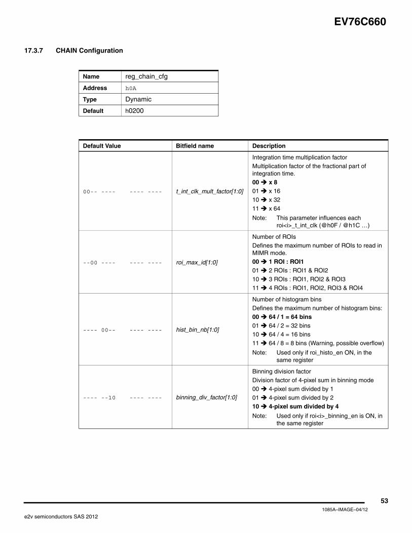
17.3.7 CHAIN Configuration
Name reg_chain_cfg
Address h0A
Type Dynamic
Default h0200
Default Value Bitfield name Description
00-- ---- ---- ---- t_int_clk_mult_factor[1:0]
Integration time multiplication factor
Multiplication factor of the fractional part of integration time.
00 x 801 x 16
10 x 32
11 x 64
Note: This parameter influences each roi<i>_t_int_clk (@h0F / @h1C …)
--00 ---- ---- ---- roi_max_id[1:0]
Number of ROIsDefines the maximum number of ROIs to read in MIMR mode.00 1 ROI : ROI101 2 ROIs : ROI1 & ROI2
10 3 ROIs : ROI1, ROI2 & ROI311 4 ROIs : ROI1, ROI2, ROI3 & ROI4
---- 00-- ---- ---- hist_bin_nb[1:0]
Number of histogram binsDefines the maximum number of histogram bins:
00 64 / 1 = 64 bins01 64 / 2 = 32 bins10 64 / 4 = 16 bins
11 64 / 8 = 8 bins (Warning, possible overflow)
Note: Used only if roi_histo_en ON, in the same register
---- --10 ---- ---- binning_div_factor[1:0]
Binning division factor
Division factor of 4-pixel sum in binning mode 00 4-pixel sum divided by 1
01 4-pixel sum divided by 2
10 4-pixel sum divided by 4
Note: Used only if roi<i>_binning_en is ON, in the same register
531085A–IMAGE–04/12
e2v semiconductors SAS 2012
EV76C660
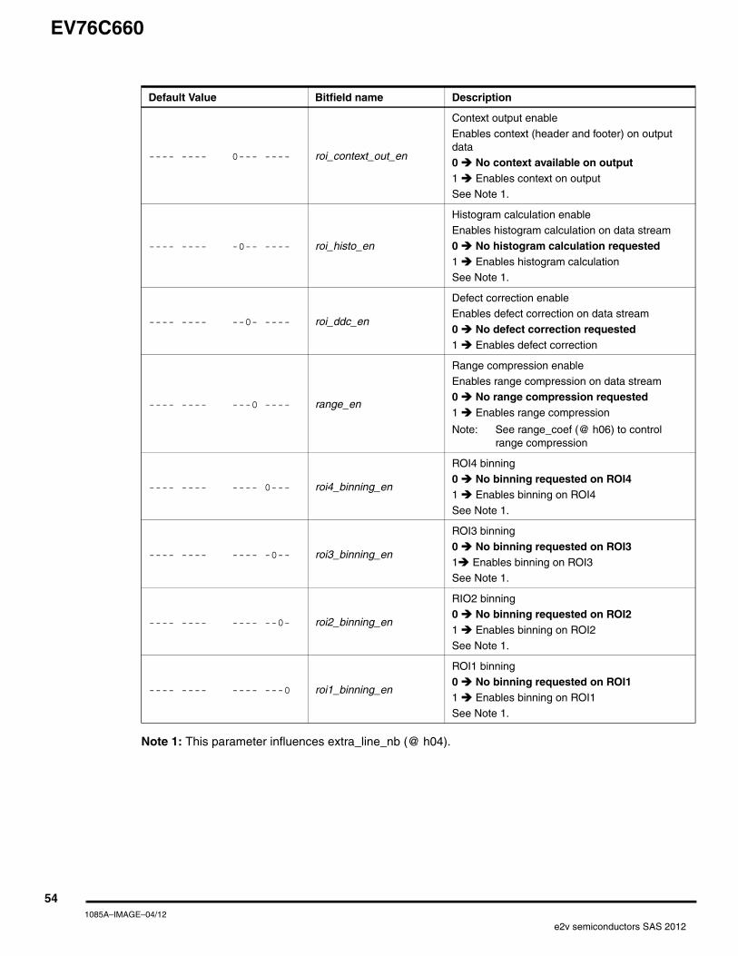
Note 1: This parameter influences extra_line_nb (@ h04).
---- ---- 0--- ---- roi_context_out_en
Context output enable
Enables context (header and footer) on output data
0 No context available on output1 Enables context on outputSee Note 1.
---- ---- -0-- ---- roi_histo_en
Histogram calculation enableEnables histogram calculation on data stream
0 No histogram calculation requested 1 Enables histogram calculationSee Note 1.
---- ---- --0- ---- roi_ddc_en
Defect correction enableEnables defect correction on data stream
0 No defect correction requested 1 Enables defect correction
---- ---- ---0 ---- range_en
Range compression enable
Enables range compression on data stream 0 No range compression requested 1 Enables range compression
Note: See range_coef (@ h06) to control range compression
---- ---- ---- 0--- roi4_binning_en
ROI4 binning
0 No binning requested on ROI41 Enables binning on ROI4
See Note 1.
---- ---- ---- -0-- roi3_binning_en
ROI3 binning
0 No binning requested on ROI31 Enables binning on ROI3See Note 1.
---- ---- ---- --0- roi2_binning_en
RIO2 binning0 No binning requested on ROI21 Enables binning on ROI2
See Note 1.
---- ---- ---- ---0 roi1_binning_en
ROI1 binning
0 No binning requested on ROI11 Enables binning on ROI1
See Note 1.
Default Value Bitfield name Description
541085A–IMAGE–04/12
e2v semiconductors SAS 2012
EV76C660
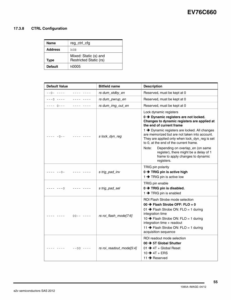
17.3.8 CTRL Configuration
Name reg_ctrl_cfg
Address h0B
TypeMixed: Static (s) and Restricted Static (rs)
Default h0005
Default Value Bitfield name Description
--0- ---- ---- ---- rs dum_stdby_en Reserved, must be kept at 0
---0 ---- ---- ---- rs dum_pwrup_en Reserved, must be kept at 0
---- 0--- ---- ---- rs dum_img_out_en Reserved, must be kept at 0
---- -0-- ---- ---- s lock_dyn_reg
Lock dynamic registers
0 Dynamic registers are not locked. Changes to dynamic registers are applied at the end of current frame1 Dynamic registers are locked. All changes are memorized but are not taken into account. They are applied only when lock_dyn_reg is set to 0, at the end of the current frame.
Note: Depending on overlap_en (on same register), there might be a delay of 1 frame to apply changes to dynamic registers.
---- --0- ---- ---- s trig_pad_inv
TRIG pin polarity
0 TRIG pin is active high 1 TRIG pin is active low
---- ---0 ---- ---- s trig_pad_selTRIG pin enable0 TRIG pin is disabled. 1 TRIG pin is enabled
---- ---- 00-- ---- rs roi_flash_mode[7:6]
ROI Flash Strobe mode selection
00 Flash Strobe OFF: FLO = 001 Flash Strobe ON: FLO = 1 during integration time
10 Flash Strobe ON: FLO = 1 during integration time + readout
11 Flash Strobe ON: FLO = 1 during acquisition sequence
---- ---- --00 ---- rs roi_readout_mode[5:4]
ROI readout mode selection
00 5T Global Shutter01 4T + Global Reset
10 4T + ERS11 Reserved
551085A–IMAGE–04/12
e2v semiconductors SAS 2012
EV76C660
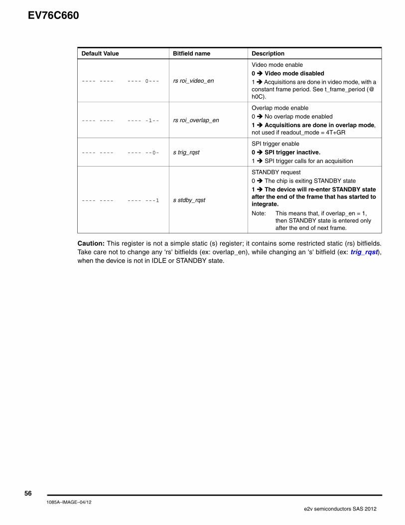
Caution: This register is not a simple static (s) register; it contains some restricted static (rs) bitfields.Take care not to change any 'rs' bitfields (ex: overlap_en), while changing an 's' bitfield (ex: trig_rqst),when the device is not in IDLE or STANDBY state.
---- ---- ---- 0--- rs roi_video_en
Video mode enable
0 Video mode disabled1 Acquisitions are done in video mode, with a constant frame period. See t_frame_period (@ h0C).
---- ---- ---- -1-- rs roi_overlap_en
Overlap mode enable0 No overlap mode enabled
1 Acquisitions are done in overlap mode, not used if readout_mode = 4T+GR
---- ---- ---- --0- s trig_rqstSPI trigger enable0 SPI trigger inactive.1 SPI trigger calls for an acquisition
---- ---- ---- ---1 s stdby_rqst
STANDBY request
0 The chip is exiting STANDBY state
1 The device will re-enter STANDBY state after the end of the frame that has started to integrate.
Note: This means that, if overlap_en = 1, then STANDBY state is entered only after the end of next frame.
Default Value Bitfield name Description
561085A–IMAGE–04/12
e2v semiconductors SAS 2012
EV76C660
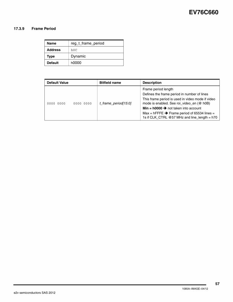
17.3.9 Frame Period
Name reg_t_frame_period
Address h0C
Type Dynamic
Default h0000
Default Value Bitfield name Description
0000 0000 0000 0000 t_frame_period[15:0]
Frame period length
Defines the frame period in number of linesThis frame period is used in video mode if video mode is enabled. See roi_video_en (@ h0B)Min = h0000 not taken into account
Max = hFFFE Frame period of 65534 lines = 1s if CLK_CTRL @57 MHz and line_length = h70
571085A–IMAGE–04/12
e2v semiconductors SAS 2012
EV76C660
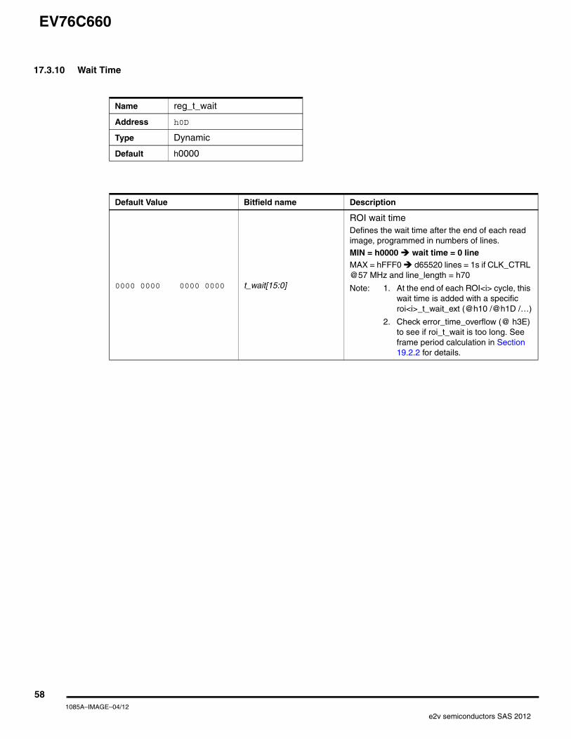
17.3.10 Wait Time
Name reg_t_wait
Address h0D
Type Dynamic
Default h0000
Default Value Bitfield name Description
0000 0000 0000 0000 t_wait[15:0]
ROI wait timeDefines the wait time after the end of each read image, programmed in numbers of lines.
MIN = h0000 wait time = 0 lineMAX = hFFF0 d65520 lines = 1s if CLK_CTRL @57 MHz and line_length = h70
Note: 1. At the end of each ROI<i> cycle, this wait time is added with a specific roi<i>_t_wait_ext (@h10 /@h1D /…)
2. Check error_time_overflow (@ h3E) to see if roi_t_wait is too long. See frame period calculation in Section 19.2.2 for details.
581085A–IMAGE–04/12
e2v semiconductors SAS 2012
EV76C660
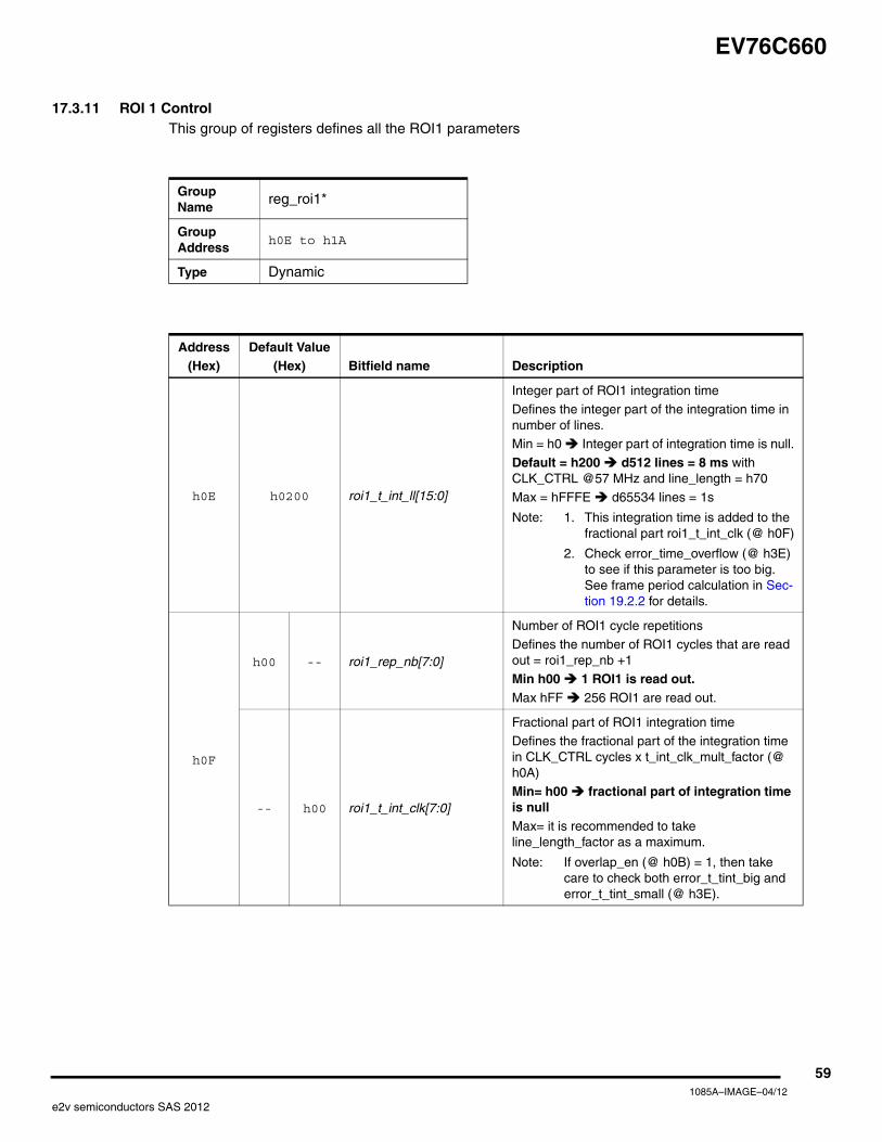
17.3.11 ROI 1 ControlThis group of registers defines all the ROI1 parameters
Group Name
reg_roi1*
Group Address
h0E to h1A
Type Dynamic
Address(Hex)
Default Value(Hex) Bitfield name Description
h0E h0200 roi1_t_int_ll[15:0]
Integer part of ROI1 integration timeDefines the integer part of the integration time in number of lines.Min = h0 Integer part of integration time is null.
Default = h200 d512 lines = 8 ms with CLK_CTRL @57 MHz and line_length = h70
Max = hFFFE d65534 lines = 1s
Note: 1. This integration time is added to the fractional part roi1_t_int_clk (@ h0F)
2. Check error_time_overflow (@ h3E) to see if this parameter is too big. See frame period calculation in Sec-tion 19.2.2 for details.
h0F
h00 -- roi1_rep_nb[7:0]
Number of ROI1 cycle repetitions
Defines the number of ROI1 cycles that are read out = roi1_rep_nb +1
Min h00 1 ROI1 is read out.Max hFF 256 ROI1 are read out.
-- h00 roi1_t_int_clk[7:0]
Fractional part of ROI1 integration time
Defines the fractional part of the integration time in CLK_CTRL cycles x t_int_clk_mult_factor (@ h0A)
Min= h00 fractional part of integration time is nullMax= it is recommended to take line_length_factor as a maximum.
Note: If overlap_en (@ h0B) = 1, then take care to check both error_t_tint_big and error_t_tint_small (@ h3E).
591085A–IMAGE–04/12
e2v semiconductors SAS 2012
EV76C660
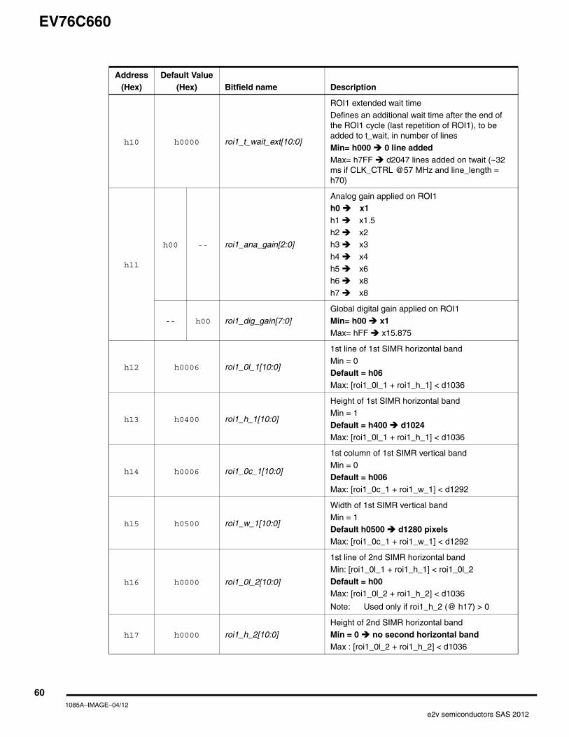
h10 h0000 roi1_t_wait_ext[10:0]
ROI1 extended wait timeDefines an additional wait time after the end of the ROI1 cycle (last repetition of ROI1), to be added to t_wait, in number of lines
Min= h000 0 line addedMax= h7FF d2047 lines added on twait (~32 ms if CLK_CTRL @57 MHz and line_length = h70)
h11
h00 -- roi1_ana_gain[2:0]
Analog gain applied on ROI1h0 x1h1 x1.5
h2 x2h3 x3
h4 x4
h5 x6h6 x8
h7 x8
-- h00 roi1_dig_gain[7:0]
Global digital gain applied on ROI1
Min= h00 x1Max= hFF x15.875
h12 h0006 roi1_0l_1[10:0]
1st line of 1st SIMR horizontal band
Min = 0Default = h06Max: [roi1_0l_1 + roi1_h_1] < d1036
h13 h0400 roi1_h_1[10:0]
Height of 1st SIMR horizontal band
Min = 1
Default = h400 d1024Max: [roi1_0l_1 + roi1_h_1] < d1036
h14 h0006 roi1_0c_1[10:0]
1st column of 1st SIMR vertical bandMin = 0
Default = h006Max: [roi1_0c_1 + roi1_w_1] < d1292
h15 h0500 roi1_w_1[10:0]
Width of 1st SIMR vertical band
Min = 1Default h0500 d1280 pixelsMax: [roi1_0c_1 + roi1_w_1] < d1292
h16 h0000 roi1_0l_2[10:0]
1st line of 2nd SIMR horizontal band
Min: [roi1_0l_1 + roi1_h_1] < roi1_0l_2
Default = h00Max: [roi1_0l_2 + roi1_h_2] < d1036
Note: Used only if roi1_h_2 (@ h17) > 0
h17 h0000 roi1_h_2[10:0]
Height of 2nd SIMR horizontal band
Min = 0 no second horizontal bandMax : [roi1_0l_2 + roi1_h_2] < d1036
Address(Hex)
Default Value(Hex) Bitfield name Description
601085A–IMAGE–04/12
e2v semiconductors SAS 2012
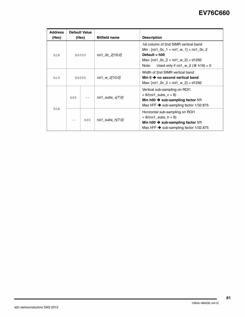
EV76C660
h18 h0000 roi1_0c_2[10:0]
1st column of 2nd SIMR vertical bandMin : [roi1_0c_1 + roi1_w_1] < roi1_0c_2
Default = h00Max: [roi1_0c_2 + roi1_w_2] < d1292
Note: Used only if roi1_w_2 (@ h19) > 0
h19 h0000 roi1_w_2[10:0]Width of 2nd SIMR vertical bandMin 0 no second vertical bandMax: [roi1_0c_2 + roi1_w_2] < d1292
h1A
h00 -- roi1_subs_v[7:0]
Vertical sub-sampling on ROI1
= 8/(roi1_subs_v + 8)
Min h00 sub-sampling factor 1/1Max hFF sub-sampling factor 1/32.875
-- h00 roi1_subs_h[7:0]
Horizontal sub-sampling on ROI1= 8/(roi1_subs_h + 8)
Min h00 sub-sampling factor 1/1Max hFF sub-sampling factor 1/32.875
Address(Hex)
Default Value(Hex) Bitfield name Description
611085A–IMAGE–04/12
e2v semiconductors SAS 2012
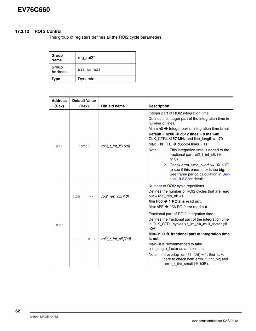
EV76C660
17.3.12 ROI 2 ControlThis group of registers defines all the ROI2 cycle parameters
Group Name
reg_roi2*
Group Address
h1B to h23
Type Dynamic
Address(Hex)
Default Value(Hex) Bitfield name Description
h1B h0200 roi2_t_int_ll[15:0]
Integer part of ROI2 integration timeDefines the integer part of the integration time in number of lines.Min = h0 Integer part of integration time is null.
Default = h200 d512 lines = 8 ms with CLK_CTRL @57 MHz and line_length = h70
Max = hFFFE d65534 lines = 1s
Note: 1. This integration time is added to the fractional part roi2_t_int_clk (@ h1C)
2. Check error_time_overflow (@ h3E) to see if this parameter is too big. See frame period calculation in Sec-tion 19.2.2 for details.
h1C
h00 -- roi2_rep_nb[7:0]
Number of ROI2 cycle repetitionsDefines the number of ROI2 cycles that are read out = roi2_rep_nb +1 Min h00 1 ROI2 is read out.Max hFF 256 ROI2 are read out.
-- h00 roi2_t_int_clk[7:0]
Fractional part of ROI2 integration time
Defines the fractional part of the integration time in CLK_CTRL cycles x t_int_clk_mult_factor (@ h0A) Min= h00 fractional part of integration time is nullMax= it is recommended to take line_length_factor as a maximum.
Note: If overlap_en (@ h0B) = 1, then take care to check both error_t_tint_big and error_t_tint_small (@ h3E).
621085A–IMAGE–04/12
e2v semiconductors SAS 2012

EV76C660
h1D h0000 roi2_t_wait_ext[10:0]
ROI2 extended wait timeDefines an additional wait time after the end of the ROI2 cycle (last repetition of ROI2), to be added to t_wait, in number of lines
Min= h000 0 line addedMax= h7FF d2047 lines added on twait (~ 32 ms if CLK_CTRL @57 MHz and line_length = h70)
h1E
h00 -- roi2_ana_gain[2:0]
Analog gain applied on ROI2h0 x1h1 x1.5
h2 x2h3 x3
h4 x4
h5 x6h6 x8
h7 x8
-- h00 roi2_dig_gain[7:0]
Global digital gain applied on ROI2
Min= h00 x1Max= hFF x15.875
h1F h0006 roi2_0l_1[10:0]
1st line of ROI2
Min = 0Default = h06Max: [roi2_0l_1 + roi2_h_1] < d1036
h20 h0400 roi2_h_1[10:0]
Height of ROI2
Min = 1
Default = h400 d1024Max: [roi2_0l_1 + roi2_h_1] < d1036
h21 h0006 roi2_0c_1[10:0]
1st column of ROI2Min = 0
Default = h006Max: [roi2_0c_1 + roi2_w_1] < d1292
h22 h0500 roi2_w_1[10:0]
Width of ROI2
Min = 1Default h0500 d1280 pixelsMax: [roi2_0c_1 + roi2_w_1] < d1292
h23
h00 -- roi2_subs_v[7:0]
Vertical sub-sampling on ROI2
= 8/(roi2_subs_v + 8)
Min h00 sub-sampling factor 1/1Max hFF sub-sampling factor 1/32.875
-- h00 roi2_subs_h[7:0]
Horizontal sub-sampling on ROI2
= 8/(roi2_subs_h + 8)Min h00 sub-sampling factor 1/1Max hFF sub-sampling factor 1/32.875
Address(Hex)
Default Value(Hex) Bitfield name Description
631085A–IMAGE–04/12
e2v semiconductors SAS 2012
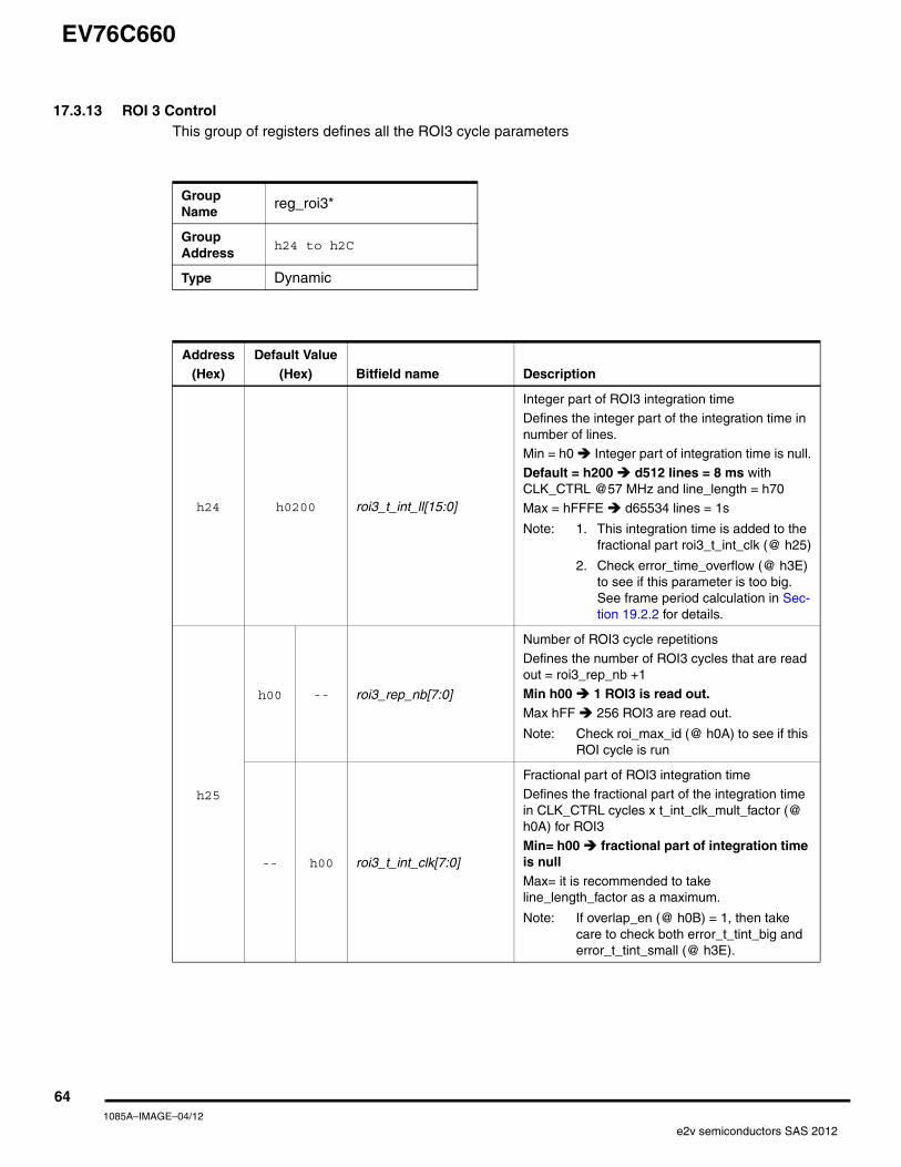
EV76C660
17.3.13 ROI 3 ControlThis group of registers defines all the ROI3 cycle parameters
Group Name
reg_roi3*
Group Address
h24 to h2C
Type Dynamic
Address(Hex)
Default Value(Hex) Bitfield name Description
h24 h0200 roi3_t_int_ll[15:0]
Integer part of ROI3 integration timeDefines the integer part of the integration time in number of lines.Min = h0 Integer part of integration time is null.
Default = h200 d512 lines = 8 ms with CLK_CTRL @57 MHz and line_length = h70
Max = hFFFE d65534 lines = 1s
Note: 1. This integration time is added to the fractional part roi3_t_int_clk (@ h25)
2. Check error_time_overflow (@ h3E) to see if this parameter is too big. See frame period calculation in Sec-tion 19.2.2 for details.
h25
h00 -- roi3_rep_nb[7:0]
Number of ROI3 cycle repetitions
Defines the number of ROI3 cycles that are read out = roi3_rep_nb +1
Min h00 1 ROI3 is read out.Max hFF 256 ROI3 are read out.
Note: Check roi_max_id (@ h0A) to see if this ROI cycle is run
-- h00 roi3_t_int_clk[7:0]
Fractional part of ROI3 integration timeDefines the fractional part of the integration time in CLK_CTRL cycles x t_int_clk_mult_factor (@ h0A) for ROI3
Min= h00 fractional part of integration time is nullMax= it is recommended to take line_length_factor as a maximum.
Note: If overlap_en (@ h0B) = 1, then take care to check both error_t_tint_big and error_t_tint_small (@ h3E).
641085A–IMAGE–04/12
e2v semiconductors SAS 2012
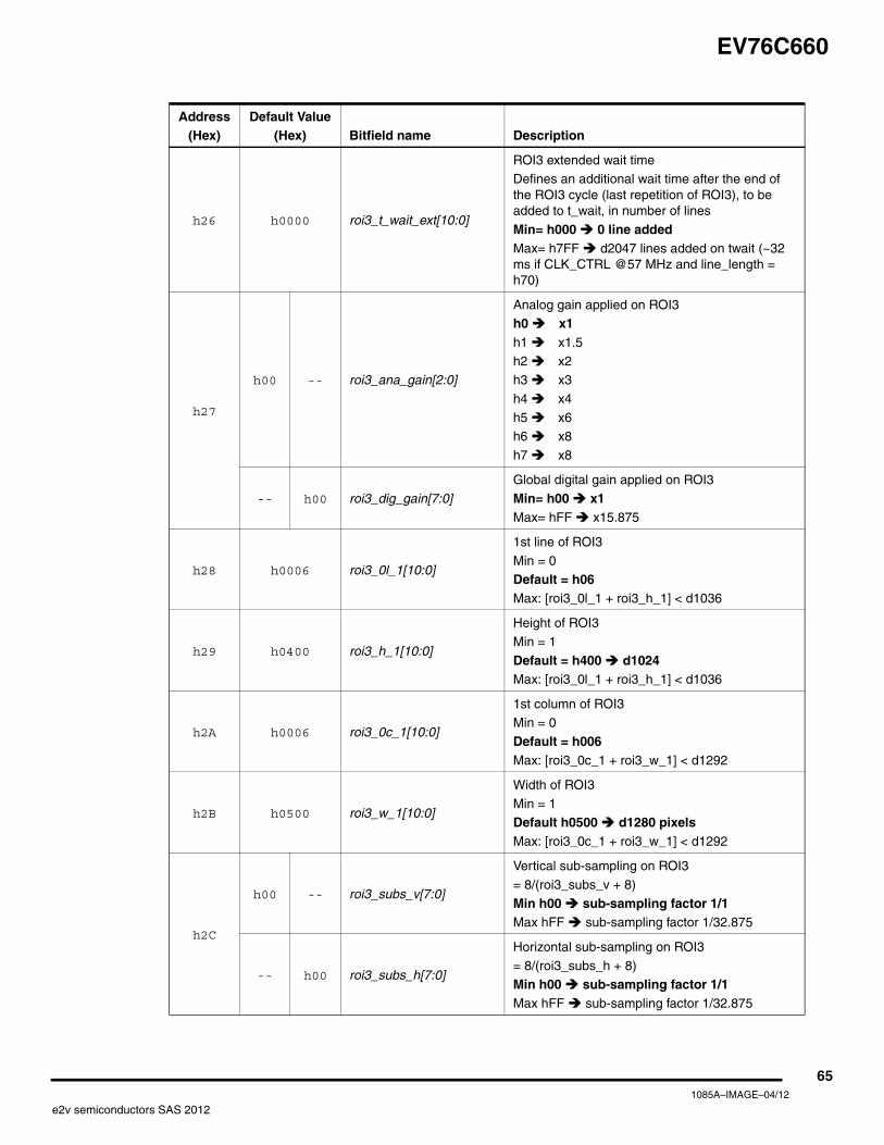
EV76C660
h26 h0000 roi3_t_wait_ext[10:0]
ROI3 extended wait timeDefines an additional wait time after the end of the ROI3 cycle (last repetition of ROI3), to be added to t_wait, in number of lines
Min= h000 0 line addedMax= h7FF d2047 lines added on twait (~32 ms if CLK_CTRL @57 MHz and line_length = h70)
h27
h00 -- roi3_ana_gain[2:0]
Analog gain applied on ROI3h0 x1h1 x1.5
h2 x2h3 x3
h4 x4
h5 x6h6 x8
h7 x8
-- h00 roi3_dig_gain[7:0]
Global digital gain applied on ROI3
Min= h00 x1Max= hFF x15.875
h28 h0006 roi3_0l_1[10:0]
1st line of ROI3
Min = 0Default = h06Max: [roi3_0l_1 + roi3_h_1] < d1036
h29 h0400 roi3_h_1[10:0]
Height of ROI3
Min = 1
Default = h400 d1024Max: [roi3_0l_1 + roi3_h_1] < d1036
h2A h0006 roi3_0c_1[10:0]
1st column of ROI3Min = 0
Default = h006Max: [roi3_0c_1 + roi3_w_1] < d1292
h2B h0500 roi3_w_1[10:0]
Width of ROI3
Min = 1Default h0500 d1280 pixelsMax: [roi3_0c_1 + roi3_w_1] < d1292
h2C
h00 -- roi3_subs_v[7:0]
Vertical sub-sampling on ROI3
= 8/(roi3_subs_v + 8)
Min h00 sub-sampling factor 1/1Max hFF sub-sampling factor 1/32.875
-- h00 roi3_subs_h[7:0]
Horizontal sub-sampling on ROI3
= 8/(roi3_subs_h + 8)Min h00 sub-sampling factor 1/1Max hFF sub-sampling factor 1/32.875
Address(Hex)
Default Value(Hex) Bitfield name Description
651085A–IMAGE–04/12
e2v semiconductors SAS 2012
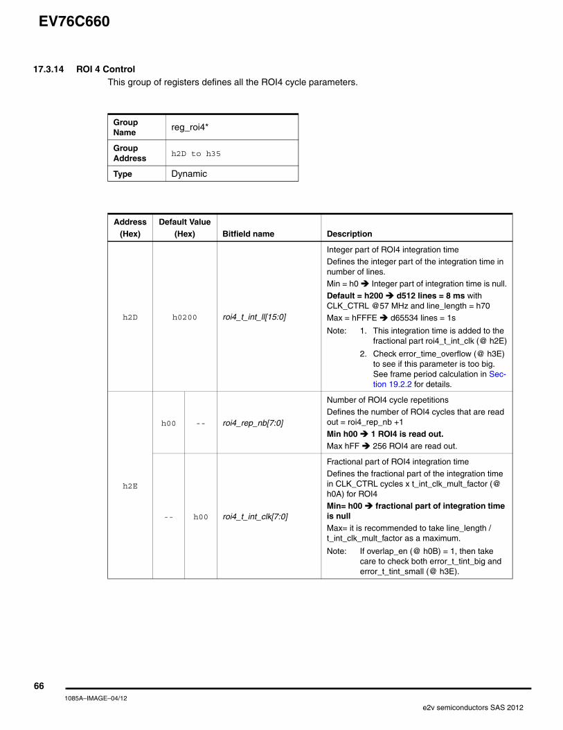
EV76C660
17.3.14 ROI 4 ControlThis group of registers defines all the ROI4 cycle parameters.
Group Name
reg_roi4*
Group Address
h2D to h35
Type Dynamic
Address(Hex)
Default Value(Hex) Bitfield name Description
h2D h0200 roi4_t_int_ll[15:0]
Integer part of ROI4 integration timeDefines the integer part of the integration time in number of lines.Min = h0 Integer part of integration time is null.
Default = h200 d512 lines = 8 ms with CLK_CTRL @57 MHz and line_length = h70
Max = hFFFE d65534 lines = 1s
Note: 1. This integration time is added to the fractional part roi4_t_int_clk (@ h2E)
2. Check error_time_overflow (@ h3E) to see if this parameter is too big. See frame period calculation in Sec-tion 19.2.2 for details.
h2E
h00 -- roi4_rep_nb[7:0]
Number of ROI4 cycle repetitions
Defines the number of ROI4 cycles that are read out = roi4_rep_nb +1
Min h00 1 ROI4 is read out.Max hFF 256 ROI4 are read out.
-- h00 roi4_t_int_clk[7:0]
Fractional part of ROI4 integration time
Defines the fractional part of the integration time in CLK_CTRL cycles x t_int_clk_mult_factor (@ h0A) for ROI4
Min= h00 fractional part of integration time is nullMax= it is recommended to take line_length / t_int_clk_mult_factor as a maximum.
Note: If overlap_en (@ h0B) = 1, then take care to check both error_t_tint_big and error_t_tint_small (@ h3E).
661085A–IMAGE–04/12
e2v semiconductors SAS 2012

EV76C660
h2F h0000 roi4_t_wait_ext[10:0]
ROI4 extended wait timeDefines an additional wait time after the end of the ROI4 cycle (last repetition of ROI4), to be added to t_wait, in number of lines
Min= h000 0 line addedMax= h7FF d2047 lines added on twait (~32 ms if CLK_CTRL @57 MHz and line_length = h70)
h30
h00 -- roi4_ana_gain[2:0]
Analog gain applied on ROI4h0 x1h1 x1.5
h2 x2h3 x3
h4 x4
h5 x6h6 x8
h7 x8
-- h00 roi4_dig_gain[7:0]
Global digital gain applied on ROI4
Min= h00 x1Max= hFF x15.875
h31 h0006 roi4_0l_1[10:0]
1st line of ROI4
Min = 0Default = h06Max: [roi4_0l_1 + roi4_h_1] < d1036
h32 h0400 roi4_h_1[10:0]
Height of ROI4
Min = 1
Default = h400 d1024Max: [roi4_0l_1 + roi4_h_1] < d1036
h33 h0006 roi4_0c_1[10:0]
1st column of ROI4Min = 0
Default = h006Max: [roi4_0c_1 + roi4_w_1] < d1292
h34 h0500 roi4_w_1[10:0]
Width of ROI4
Min = 1Default h0500 d1280 pixelsMax: [roi4_0c_1 + roi4_w_1] < d1292
h35
h00 -- roi4_subs_v[7:0]
Vertical sub-sampling on ROI4
= 8/(roi4_subs_v + 8)
Min h00 sub-sampling factor 1/1Max hFF sub-sampling factor 1/32.875
-- h00 roi4_subs_h[7:0]
Horizontal sub-sampling on ROI4
= 8/(roi4_subs_h + 8)Min h00 sub-sampling factor 1/1Max hFF sub-sampling factor 1/32.875
Address(Hex)
Default Value(Hex) Bitfield name Description
671085A–IMAGE–04/12
e2v semiconductors SAS 2012
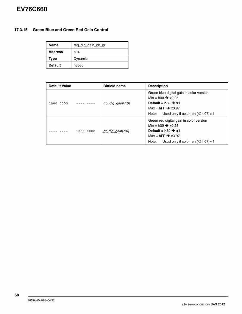
EV76C660
17.3.15 Green Blue and Green Red Gain Control
Name reg_dig_gain_gb_gr
Address h36
Type Dynamic
Default h8080
Default Value Bitfield name Description
1000 0000 ---- ---- gb_dig_gain[7:0]
Green blue digital gain in color version
Min = h00 x0.25Default = h80 x1Max = hFF x3.97
Note: Used only if color_en (@ h07)= 1
---- ---- 1000 0000 gr_dig_gain[7:0]
Green red digital gain in color versionMin = h00 x0.25
Default = h80 x1Max = hFF x3.97
Note: Used only if color_en (@ h07)= 1
681085A–IMAGE–04/12
e2v semiconductors SAS 2012
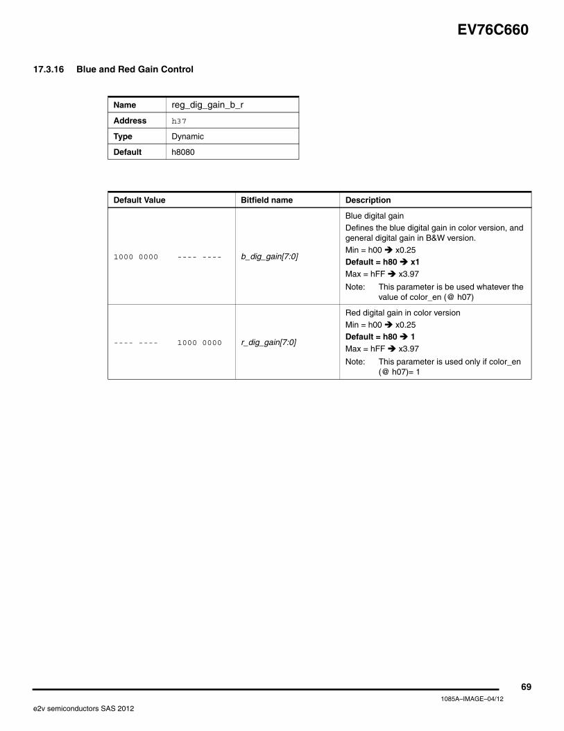
EV76C660
17.3.16 Blue and Red Gain Control
Name reg_dig_gain_b_r
Address h37
Type Dynamic
Default h8080
Default Value Bitfield name Description
1000 0000 ---- ---- b_dig_gain[7:0]
Blue digital gain
Defines the blue digital gain in color version, and general digital gain in B&W version.
Min = h00 x0.25Default = h80 x1Max = hFF x3.97
Note: This parameter is be used whatever the value of color_en (@ h07)
---- ---- 1000 0000 r_dig_gain[7:0]
Red digital gain in color version
Min = h00 x0.25Default = h80 1Max = hFF x3.97
Note: This parameter is used only if color_en (@ h07)= 1
691085A–IMAGE–04/12
e2v semiconductors SAS 2012
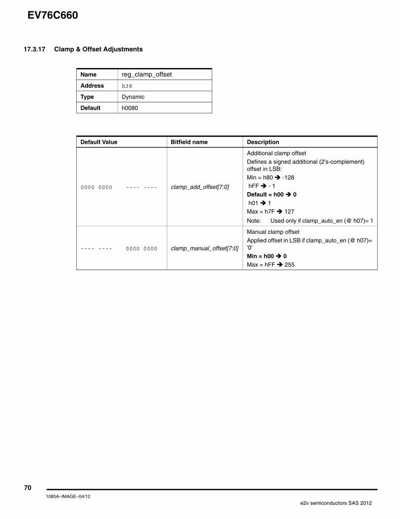
EV76C660
17.3.17 Clamp & Offset Adjustments
Name reg_clamp_offset
Address h38
Type Dynamic
Default h0080
Default Value Bitfield name Description
0000 0000 ---- ---- clamp_add_offset[7:0]
Additional clamp offset
Defines a signed additional (2's-complement) offset in LSB:
Min = h80 -128 hFF - 1
Default = h00 0 h01 1Max = h7F 127
Note: Used only if clamp_auto_en (@ h07)= 1
---- ---- 0000 0000 clamp_manual_offset[7:0]
Manual clamp offset
Applied offset in LSB if clamp_auto_en (@ h07)= '0'
Min = h00 0Max = hFF 255
701085A–IMAGE–04/12
e2v semiconductors SAS 2012
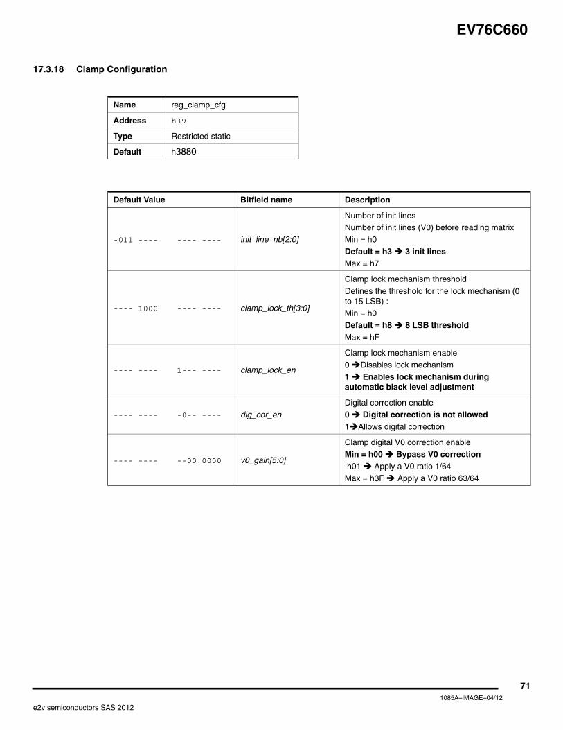
EV76C660
17.3.18 Clamp Configuration
Name reg_clamp_cfg
Address h39
Type Restricted static
Default h3880
Default Value Bitfield name Description
-011 ---- ---- ---- init_line_nb[2:0]
Number of init lines
Number of init lines (V0) before reading matrixMin = h0
Default = h3 3 init linesMax = h7
---- 1000 ---- ---- clamp_lock_th[3:0]
Clamp lock mechanism threshold
Defines the threshold for the lock mechanism (0 to 15 LSB) :
Min = h0Default = h8 8 LSB thresholdMax = hF
---- ---- 1--- ---- clamp_lock_en
Clamp lock mechanism enable
0 Disables lock mechanism
1 Enables lock mechanism during automatic black level adjustment
---- ---- -0-- ---- dig_cor_en
Digital correction enable
0 Digital correction is not allowed1 Allows digital correction
---- ---- --00 0000 v0_gain[5:0]
Clamp digital V0 correction enable
Min = h00 Bypass V0 correction h01 Apply a V0 ratio 1/64
Max = h3F Apply a V0 ratio 63/64
711085A–IMAGE–04/12
e2v semiconductors SAS 2012
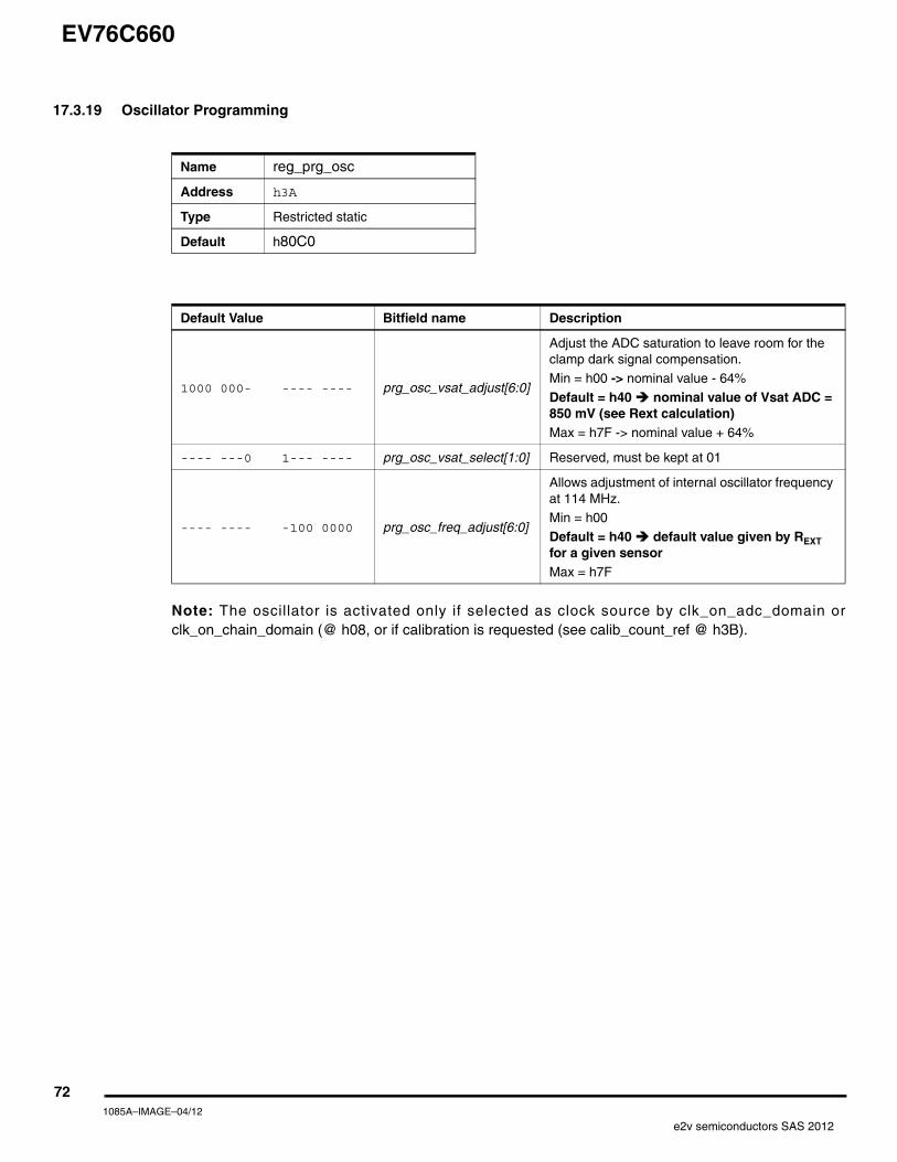
EV76C660
17.3.19 Oscillator Programming
Note: The oscillator is activated only if selected as clock source by clk_on_adc_domain orclk_on_chain_domain (@ h08, or if calibration is requested (see calib_count_ref @ h3B).
Name reg_prg_osc
Address h3A
Type Restricted static
Default h80C0
Default Value Bitfield name Description
1000 000- ---- ---- prg_osc_vsat_adjust[6:0]
Adjust the ADC saturation to leave room for the clamp dark signal compensation.
Min = h00 -> nominal value - 64%
Default = h40 nominal value of Vsat ADC = 850 mV (see Rext calculation)Max = h7F -> nominal value + 64%
---- ---0 1--- ---- prg_osc_vsat_select[1:0] Reserved, must be kept at 01
---- ---- -100 0000 prg_osc_freq_adjust[6:0]
Allows adjustment of internal oscillator frequency at 114 MHz.Min = h00
Default = h40 default value given by REXT for a given sensorMax = h7F
721085A–IMAGE–04/12
e2v semiconductors SAS 2012
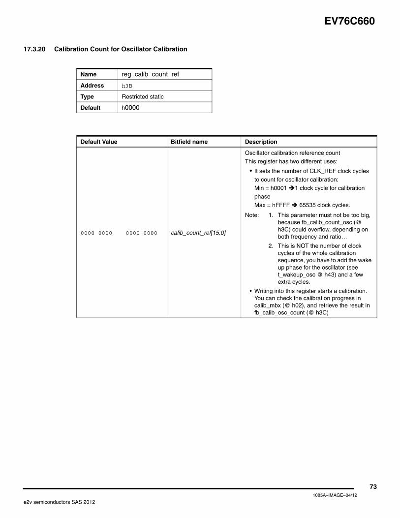
EV76C660
17.3.20 Calibration Count for Oscillator Calibration
Name reg_calib_count_ref
Address h3B
Type Restricted static
Default h0000
Default Value Bitfield name Description
0000 0000 0000 0000 calib_count_ref[15:0]
Oscillator calibration reference count
This register has two different uses:
• It sets the number of CLK_REF clock cycles
to count for oscillator calibration: Min = h0001 1 clock cycle for calibration
phase
Max = hFFFF 65535 clock cycles.
Note: 1. This parameter must not be too big, because fb_calib_count_osc (@ h3C) could overflow, depending on both frequency and ratio…
2. This is NOT the number of clock cycles of the whole calibration sequence, you have to add the wake up phase for the oscillator (see t_wakeup_osc @ h43) and a few extra cycles.
• Writing into this register starts a calibration. You can check the calibration progress in calib_mbx (@ h02), and retrieve the result in fb_calib_osc_count (@ h3C)
731085A–IMAGE–04/12
e2v semiconductors SAS 2012
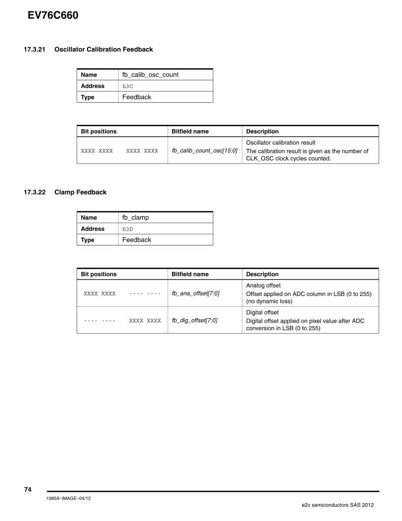
EV76C660
17.3.21 Oscillator Calibration Feedback
17.3.22 Clamp Feedback
Name fb_calib_osc_count
Address h3C
Type Feedback
Bit positions Bitfield name Description
XXXX XXXX XXXX XXXX fb_calib_count_osc[15:0]Oscillator calibration resultThe calibration result is given as the number of CLK_OSC clock cycles counted.
Name fb_clamp
Address h3D
Type Feedback
Bit positions Bitfield name Description
XXXX XXXX ---- ---- fb_ana_offset[7:0]Analog offset
Offset applied on ADC column in LSB (0 to 255) (no dynamic loss)
---- ---- XXXX XXXX fb_dig_offset[7:0]Digital offsetDigital offset applied on pixel value after ADC conversion in LSB (0 to 255)
741085A–IMAGE–04/12
e2v semiconductors SAS 2012
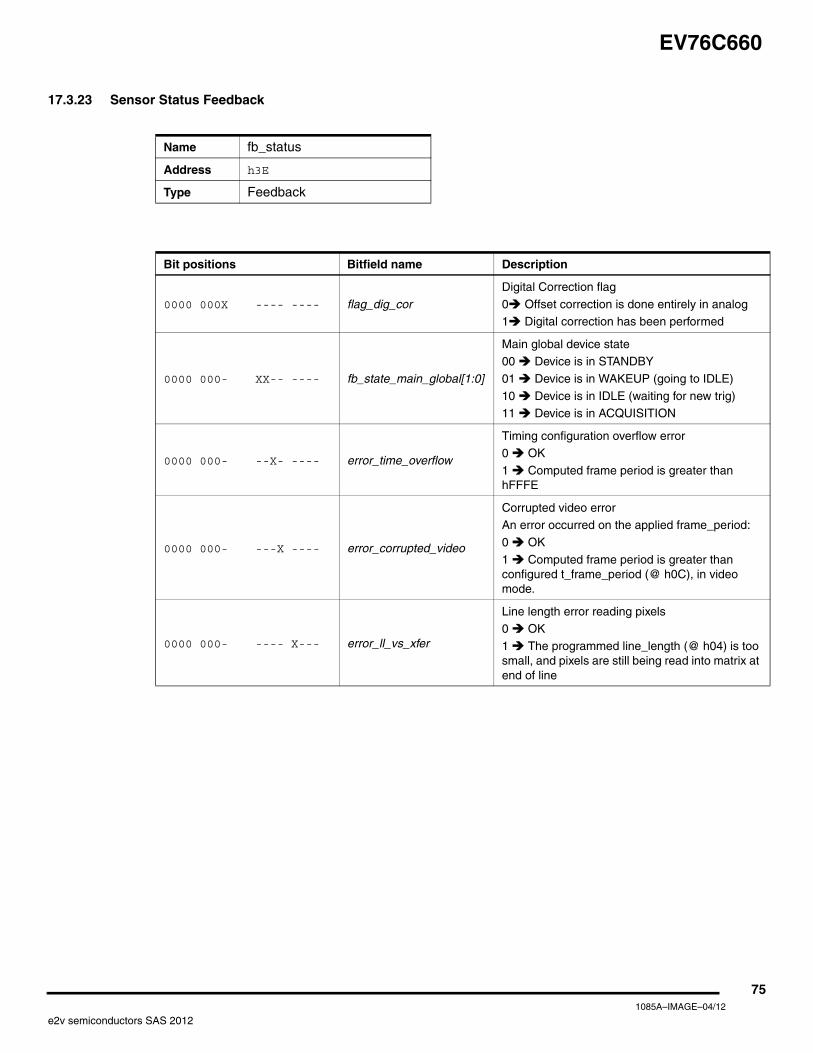
EV76C660
17.3.23 Sensor Status Feedback
Name fb_status
Address h3E
Type Feedback
Bit positions Bitfield name Description
0000 000X ---- ---- flag_dig_cor
Digital Correction flag
0 Offset correction is done entirely in analog1 Digital correction has been performed
0000 000- XX-- ---- fb_state_main_global[1:0]
Main global device state00 Device is in STANDBY
01 Device is in WAKEUP (going to IDLE)
10 Device is in IDLE (waiting for new trig)11 Device is in ACQUISITION
0000 000- --X- ---- error_time_overflow
Timing configuration overflow error0 OK
1 Computed frame period is greater than hFFFE
0000 000- ---X ---- error_corrupted_video
Corrupted video errorAn error occurred on the applied frame_period:
0 OK
1 Computed frame period is greater than configured t_frame_period (@ h0C), in video mode.
0000 000- ---- X--- error_ll_vs_xfer
Line length error reading pixels0 OK
1 The programmed line_length (@ h04) is too small, and pixels are still being read into matrix at end of line
751085A–IMAGE–04/12
e2v semiconductors SAS 2012
EV76C660
17.3.24 DATA_CLK activity
---- ---- ---- -X-- error_ll_vs_conv
Line length error during conversion
0 OK1 The programmed line_length (@ h04) is too small, and conversion is still running at end of line
---- ---- ---- --X- error_t_int_big
Integration time error on next image
An integration time error of max 1.5 µs occurred.
0 OK1 An error has been detected on the fractional part of the NEXT image integration time (the biggest one if we are in high dynamic configuration)
---- ---- ---- ---X error_t_int_small
Integration time error on current imageAn integration time error of max 1.5 µs occurred.
0 OK
1 An error has been detected on the fractional part of the CURRENT image integration time (the smallest one if we are in high dynamic configuration)
Bit positions Bitfield name Description
Name DATA_CLK activity
Address h44
Type Restricted Static
Default value Bitfield name Description
--1- ---- ---- ---- clk_out_low_pwr
Defines DATA_CLK activity:
0 DATA_CLK always active except in STANDBY state
1 DATA_CLK is active during the whole acquisition (integration, transmission and wait)
761085A–IMAGE–04/12
e2v semiconductors SAS 2012
EV76C660
17.3.25 Pixtime Read Width
17.3.26 Chip ID
Name pixtime_read_width
Address h49
Type Restricted Static
Default h7B71
Default value Bitfield name Description
0111 1011 ---- ---- pixtime_read_5t_width[7:0]Pixel timing duration in 5T mode, step is CLK_CTRL period x 2
Default = 123 clocks = 4.31 µs @57MHz
---- ---- 0111 0001 pixtime_read_4t_width[7:0]Pixel timing duration in 4T mode, step is CLK_CTRL period x 2Default = 113 clocks = 3.96 µs @57MHz
Name chip_id
Address h7F
Type Feedback
Default h0800
Default Value Bitfield Name Description
0000 1000 0000 0010 chip_id[15:0]h0802 Ruby 660 first version
771085A–IMAGE–04/12
e2v semiconductors SAS 2012
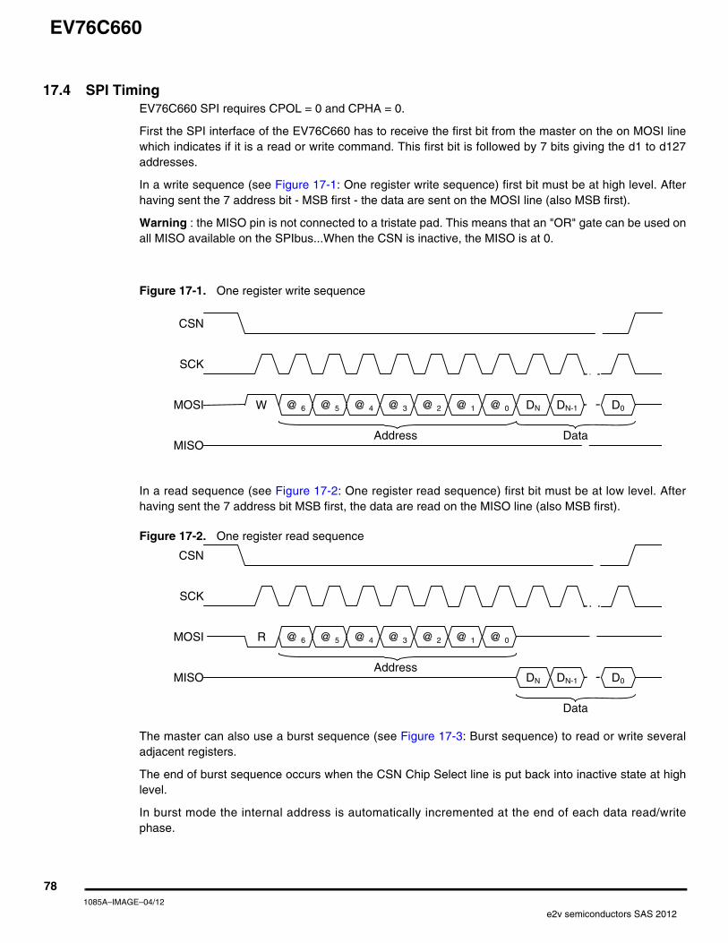
EV76C660
17.4 SPI TimingEV76C660 SPI requires CPOL = 0 and CPHA = 0.
First the SPI interface of the EV76C660 has to receive the first bit from the master on the on MOSI linewhich indicates if it is a read or write command. This first bit is followed by 7 bits giving the d1 to d127addresses.
In a write sequence (see Figure 17-1: One register write sequence) first bit must be at high level. Afterhaving sent the 7 address bit - MSB first - the data are sent on the MOSI line (also MSB first).
Warning : the MISO pin is not connected to a tristate pad. This means that an "OR" gate can be used onall MISO available on the SPIbus...When the CSN is inactive, the MISO is at 0.
Figure 17-1. One register write sequence
In a read sequence (see Figure 17-2: One register read sequence) first bit must be at low level. Afterhaving sent the 7 address bit MSB first, the data are read on the MISO line (also MSB first).
Figure 17-2. One register read sequence
The master can also use a burst sequence (see Figure 17-3: Burst sequence) to read or write severaladjacent registers.
The end of burst sequence occurs when the CSN Chip Select line is put back into inactive state at highlevel.
In burst mode the internal address is automatically incremented at the end of each data read/writephase.
@ 6 @ 5 @ 4 @ 3 @ 2 @ 1 @ 0W MOSI
SCK
DN DN-1 D0
CSN
MISO Address Data
@ 6 @ 5 @ 4 @ 3 @ 2 @ 1 @ 0R MOSI
SCK
DN DN-1 D0
CSN
MISO Address
Data
781085A–IMAGE–04/12
e2v semiconductors SAS 2012
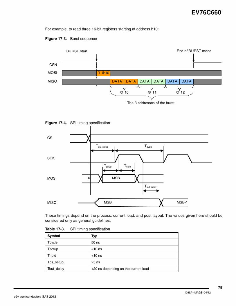
EV76C660
For example, to read three 16-bit registers starting at address h10:
Figure 17-3. Burst sequence
Figure 17-4. SPI timing specification
These timings depend on the process, current load, and post layout. The values given here should beconsidered only as general guidelines.
Table 17-3. SPI timing specification
Symbol Typ
Tcycle 50 ns
Tsetup <10 ns
Thold <10 ns
Tcs_setup >5 ns
Tout_delay <20 ns depending on the current load
R @10
DATA
CSN
MOSI
MISO DATA DATADATA DATA
@ 10 @ 11 @ 12
End of BURST mode
The 3 addresses of the burst
BURST start
DATA
TCS_setup Tcycle
CS
SCK
MOSI
MISO
Tsetup Thold
Tout_delay
MSB
MSBX
MSB-1
791085A–IMAGE–04/12
e2v semiconductors SAS 2012
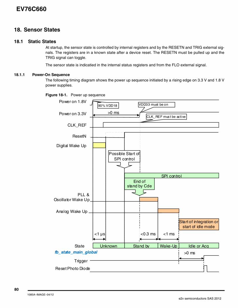
EV76C660
18. Sensor States
18.1 Static StatesAt startup, the sensor state is controlled by internal registers and by the RESETN and TRIG external sig-nals. The registers are in a known state after a device reset. The RESETN must be pulled up and theTRIG signal can toggle.
The sensor state is indicatied in the internal status registers and from the FLO external signal.
18.1.1 Power-On SequenceThe following timing diagram shows the power up sequence initiated by a rising edge on 3.3 V and 1.8 Vpower supplies.
Figure 18-1. Power up sequence
Power on 3.3V
<1 ms
CLK_REF
ResetN
Digital Wake Up
Analog Wake Up
Start of integration or start of idle mode
<1 µs
Possible Start of SPI control
PLL & Oscillator Wake Up
<0.3 ms
SPI control End of
stand by Cde
90% VDD18 VDD33 must be on
CLK_REF mus t be active
Unknown Stand by Wake-Up Idle or AcqState
Power on 1.8V
>0 ms
Trigger
Reset Photo Diode
>0 ms fb_state_main_global
801085A–IMAGE–04/12
e2v semiconductors SAS 2012
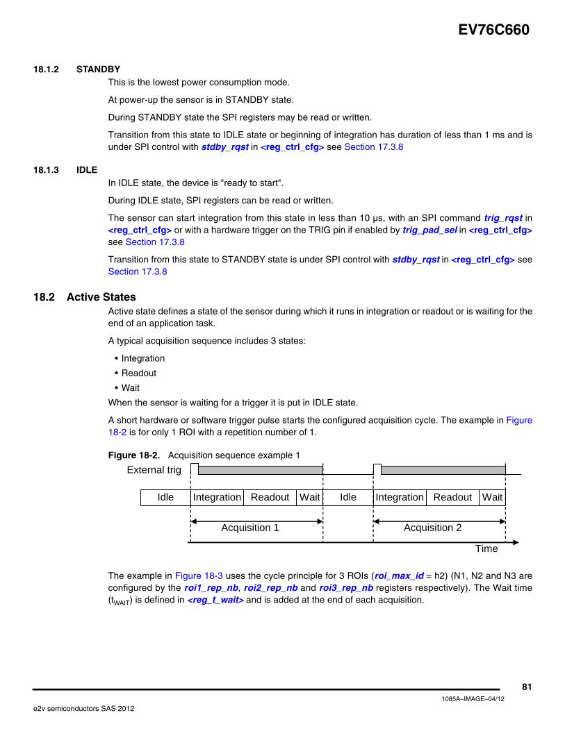
EV76C660
18.1.2 STANDBYThis is the lowest power consumption mode.
At power-up the sensor is in STANDBY state.
During STANDBY state the SPI registers may be read or written.
Transition from this state to IDLE state or beginning of integration has duration of less than 1 ms and isunder SPI control with stdby_rqst in <reg_ctrl_cfg> see Section 17.3.8
18.1.3 IDLEIn IDLE state, the device is "ready to start".
During IDLE state, SPI registers can be read or written.
The sensor can start integration from this state in less than 10 µs, with an SPI command trig_rqst in<reg_ctrl_cfg> or with a hardware trigger on the TRIG pin if enabled by trig_pad_sel in <reg_ctrl_cfg>see Section 17.3.8
Transition from this state to STANDBY state is under SPI control with stdby_rqst in <reg_ctrl_cfg> seeSection 17.3.8
18.2 Active StatesActive state defines a state of the sensor during which it runs in integration or readout or is waiting for theend of an application task.
A typical acquisition sequence includes 3 states:
• Integration
• Readout
• Wait
When the sensor is waiting for a trigger it is put in IDLE state.
A short hardware or software trigger pulse starts the configured acquisition cycle. The example in Figure18-2 is for only 1 ROI with a repetition number of 1.
Figure 18-2. Acquisition sequence example 1
The example in Figure 18-3 uses the cycle principle for 3 ROIs (roi_max_id = h2) (N1, N2 and N3 areconfigured by the roi1_rep_nb, roi2_rep_nb and roi3_rep_nb registers respectively). The Wait time(tWAIT) is defined in <reg_t_wait> and is added at the end of each acquisition.
Readout
Time
Wait
External trig
Acquisition 1
IntegrationIdle Readout Wait
Acquisition 2
Integration Idle
811085A–IMAGE–04/12
e2v semiconductors SAS 2012
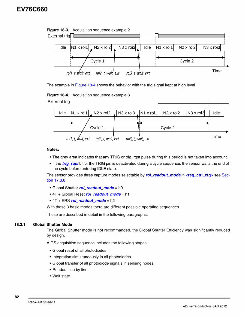
EV76C660
Figure 18-3. Acquisition sequence example 2
The example in Figure 18-4 shows the behavior with the trig signal kept at high level
Figure 18-4. Acquisition sequence example 3
Notes:
• The grey area indicates that any TRIG or trig_rqst pulse during this period is not taken into account.
• If the trig_rqst bit or the TRIG pin is deactivated during a cycle sequence, the sensor waits the end of the cycle before entering IDLE state.
The sensor provides three capture modes selectable by roi_readout_mode in <reg_ctrl_cfg> see Sec-tion 17.3.8
• Global Shutter roi_readout_mode = h0
• 4T + Global Reset roi_readout_mode = h1
• 4T + ERS roi_readout_mode = h2
With these 3 basic modes there are different possible operating sequences.
These are described in detail in the following paragraphs.
18.2.1 Global Shutter ModeThe Global Shutter mode is not recommanded, the Global Shutter Efficiency was significantly reducedby design.
A GS acquisition sequence includes the following stages:
• Global reset of all photodiodes
• Integration simultaneously in all photodiodes
• Global transfer of all photodiode signals in sensing nodes
• Readout line by line
• Wait state
Time
External trig
Cycle 1
N1 x roi1 Idle N2 x roi2 N3 x roi3
roi1_t_wait_ext
roi2_t_wait_ext roi3_t_wait_ext
Cycle 2
N1 x roi1 Idle N2 x roi2 N3 x roi3
Time
External trig
Cycle 1
N1 x roi1 Idle N2 x roi2 N3 x roi3
roi1_t_wait_ext
roi2_t_wait_ext roi3_t_wait_ext
Cycle 2
N1 x roi1 Idle N2 x roi2 N3 x roi3
821085A–IMAGE–04/12
e2v semiconductors SAS 2012
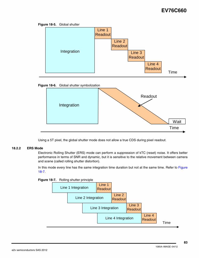
EV76C660
Figure 18-5. Global shutter
Figure 18-6. Global shutter symbolization
Using a 5T pixel, the global shutter mode does not allow a true CDS during pixel readout.
18.2.2 ERS ModeElectronic Rolling Shutter (ERS) mode can perform a suppression of kTC (reset) noise. It offers betterperformance in terms of SNR and dynamic, but it is sensitive to the relative movement between cameraand scene (called rolling shutter distortion).
In this mode every line has the same integration time duration but not at the same time. Refer to Figure18-7.
Figure 18-7. Rolling shutter principle
Time
Line 1 Readout
Integration
Line 2 Readout
Line 3 Readout
Line 4 Readout
Time Wait
Integration
Readout
Time
Line 1 ReadoutLine 1 Integration
Line 2 ReadoutLine 2 Integration
Line 3 Readout Line 3 Integration
Line 4 Readout Line 4 Integration
831085A–IMAGE–04/12
e2v semiconductors SAS 2012
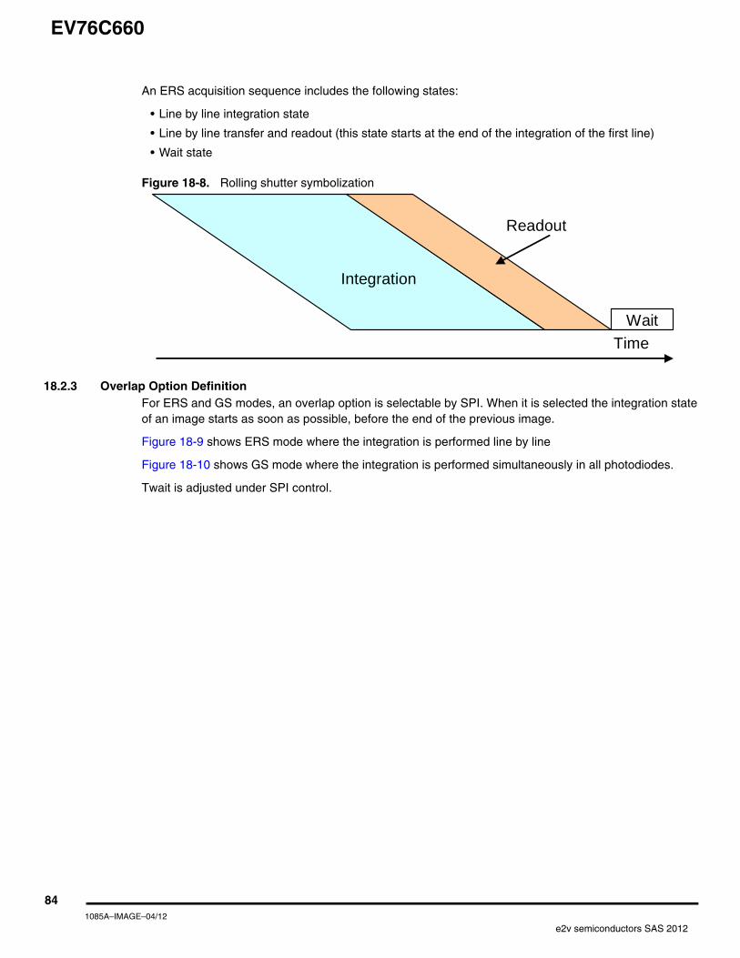
EV76C660
An ERS acquisition sequence includes the following states:
• Line by line integration state
• Line by line transfer and readout (this state starts at the end of the integration of the first line)
• Wait state
Figure 18-8. Rolling shutter symbolization
18.2.3 Overlap Option Definition For ERS and GS modes, an overlap option is selectable by SPI. When it is selected the integration stateof an image starts as soon as possible, before the end of the previous image.
Figure 18-9 shows ERS mode where the integration is performed line by line
Figure 18-10 shows GS mode where the integration is performed simultaneously in all photodiodes.
Twait is adjusted under SPI control.
Time Wait
Integration
Readout
841085A–IMAGE–04/12
e2v semiconductors SAS 2012
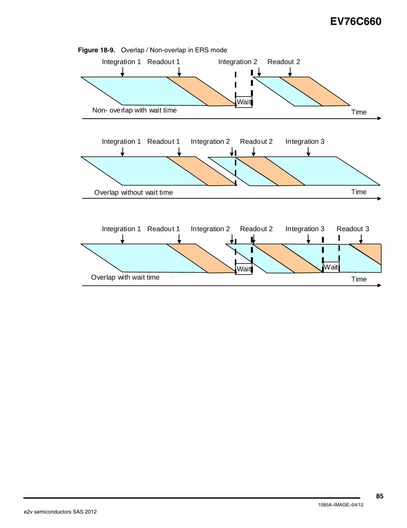
EV76C660
Figure 18-9. Overlap / Non-overlap in ERS mode
Time
Integration 1 Readout 1 Integration 2 Readout 2 Integration 3
Time Wait
Integration 1 Readout 1 Integration 2 Readout 2 Integration 3
Wait
Readout 3
Overlap without wait time
Overlap with wait time
Time Wait
Integration 1 Readout 1 Integration 2 Readout 2
Non- overlap with wait time
851085A–IMAGE–04/12
e2v semiconductors SAS 2012
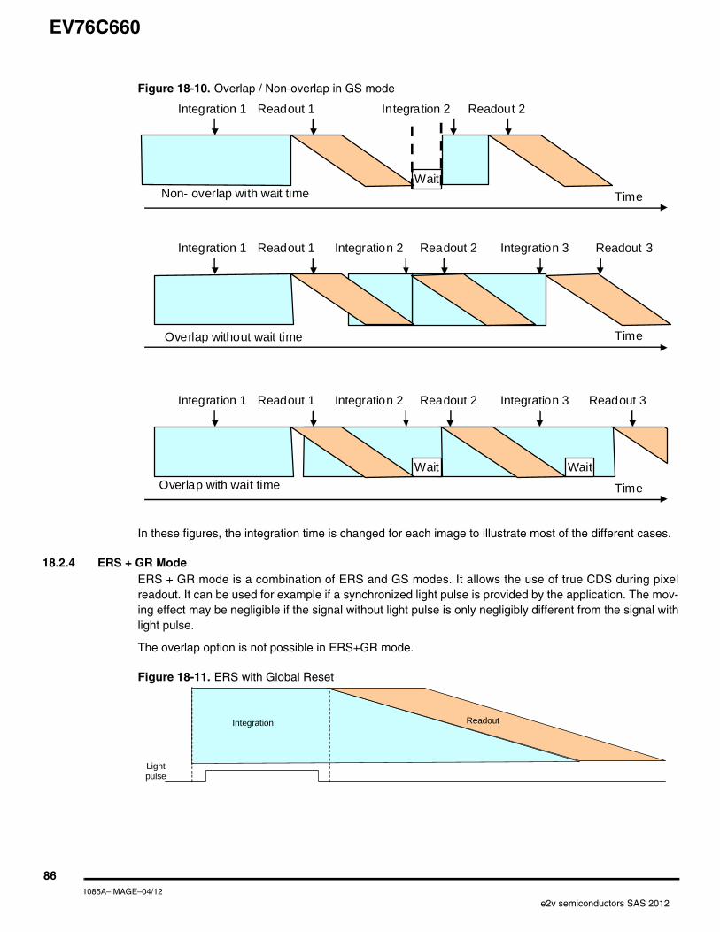
EV76C660
Figure 18-10. Overlap / Non-overlap in GS mode
In these figures, the integration time is changed for each image to illustrate most of the different cases.
18.2.4 ERS + GR ModeERS + GR mode is a combination of ERS and GS modes. It allows the use of true CDS during pixelreadout. It can be used for example if a synchronized light pulse is provided by the application. The mov-ing effect may be negligible if the signal without light pulse is only negligibly different from the signal withlight pulse.
The overlap option is not possible in ERS+GR mode.
Figure 18-11. ERS with Global Reset
Time
Integration 1 Readout 1 Integration 2 Readout 2 Integration 3
Time
Wait
Integration 1 Readout 1 Integration 2 Readout 2 Integration 3
Wait
Readout 3
Overlap without wait time
Overlap with wait time
Time Wait
Integration 1 Readout 1 Integration 2 Readout 2
Non- overlap with wait time
Readout 3
Light pulse
Integration Readout
861085A–IMAGE–04/12
e2v semiconductors SAS 2012
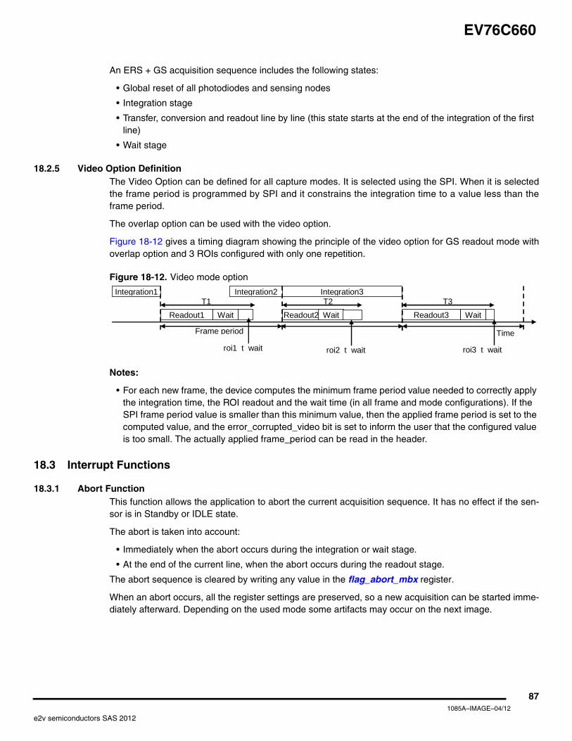
EV76C660
An ERS + GS acquisition sequence includes the following states:
• Global reset of all photodiodes and sensing nodes
• Integration stage
• Transfer, conversion and readout line by line (this state starts at the end of the integration of the first line)
• Wait stage
18.2.5 Video Option Definition The Video Option can be defined for all capture modes. It is selected using the SPI. When it is selectedthe frame period is programmed by SPI and it constrains the integration time to a value less than theframe period.
The overlap option can be used with the video option.
Figure 18-12 gives a timing diagram showing the principle of the video option for GS readout mode withoverlap option and 3 ROIs configured with only one repetition.
Figure 18-12. Video mode option
Notes:
• For each new frame, the device computes the minimum frame period value needed to correctly apply the integration time, the ROI readout and the wait time (in all frame and mode configurations). If the SPI frame period value is smaller than this minimum value, then the applied frame period is set to the computed value, and the error_corrupted_video bit is set to inform the user that the configured value is too small. The actually applied frame_period can be read in the header.
18.3 Interrupt Functions
18.3.1 Abort FunctionThis function allows the application to abort the current acquisition sequence. It has no effect if the sen-sor is in Standby or IDLE state.
The abort is taken into account:
• Immediately when the abort occurs during the integration or wait stage.
• At the end of the current line, when the abort occurs during the readout stage.
The abort sequence is cleared by writing any value in the flag_abort_mbx register.
When an abort occurs, all the register settings are preserved, so a new acquisition can be started imme-diately afterward. Depending on the used mode some artifacts may occur on the next image.
Time
Readout1 Wait
Integration1 Integration2 Integration3
Readout2 Wait Readout3 Wait
Frame period
roi1 t wait roi2 t wait roi3 t wait
T1 T2 T3
871085A–IMAGE–04/12
e2v semiconductors SAS 2012
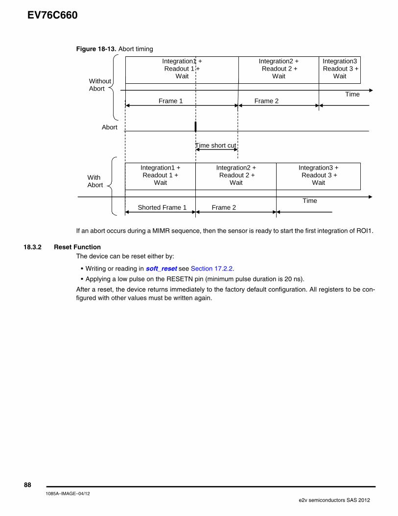
EV76C660
Figure 18-13. Abort timing
If an abort occurs during a MIMR sequence, then the sensor is ready to start the first integration of ROI1.
18.3.2 Reset FunctionThe device can be reset either by:
• Writing or reading in soft_reset see Section 17.2.2.
• Applying a low pulse on the RESETN pin (minimum pulse duration is 20 ns).
After a reset, the device returns immediately to the factory default configuration. All registers to be con-figured with other values must be written again.
Integration1 + Readout 1 +
Wait
Integration2 + Readout 2 +
Wait
Time Frame 2 Frame 1
Integration3 Readout 3 +
Wait
Abort
Time short cut
Without Abort
Integration1 + Readout 1 +
Wait
Integration2 + Readout 2 +
Wait
Time Frame 2 Shorted Frame 1
Integration3 + Readout 3 +
Wait With Abort
881085A–IMAGE–04/12
e2v semiconductors SAS 2012
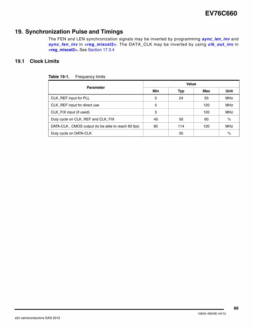
EV76C660
19. Synchronization Pulse and TimingsThe FEN and LEN synchronization signals may be inverted by programming sync_len_inv andsync_fen_inv in <reg_miscel2>. The DATA_CLK may be inverted by using clk_out_inv in<reg_miscel2>. See Section 17.3.4
19.1 Clock Limits
Table 19-1. Frequency limits
ParameterValue
Min Typ Max Unit
CLK_REF input for PLL 5 24 50 MHz
CLK_REF input for direct use 5 120 MHz
CLK_FIX input (if used) 5 120 MHz
Duty cycle on CLK_REF and CLK_FIX 40 50 60 %
DATA-CLK , CMOS output (to be able to reach 60 fps) 85 114 120 MHz
Duty cycle on DATA-CLK 50 %
891085A–IMAGE–04/12
e2v semiconductors SAS 2012
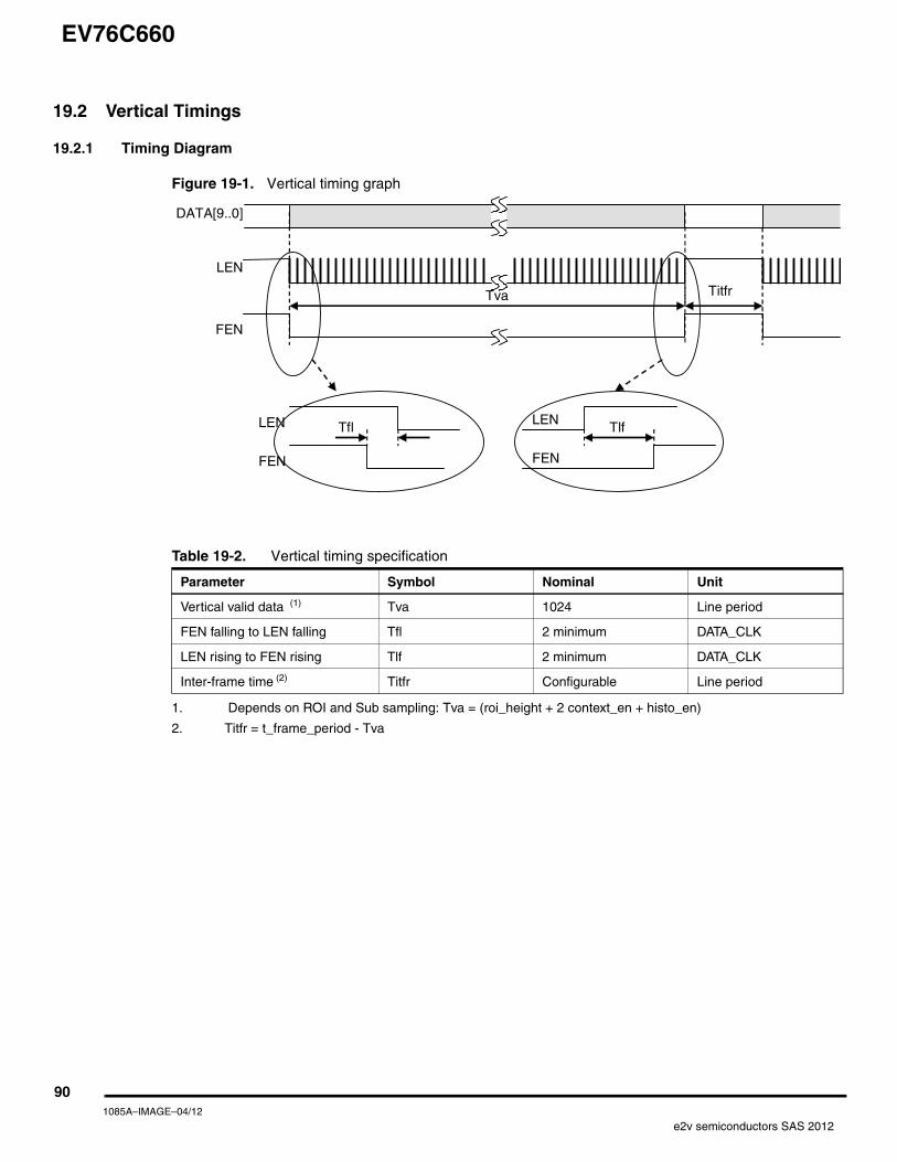
EV76C660
19.2 Vertical Timings
19.2.1 Timing Diagram
Figure 19-1. Vertical timing graph
Table 19-2. Vertical timing specification
Parameter Symbol Nominal Unit
Vertical valid data (1)
1. Depends on ROI and Sub sampling: Tva = (roi_height + 2 context_en + histo_en)
Tva 1024 Line period
FEN falling to LEN falling Tfl 2 minimum DATA_CLK
LEN rising to FEN rising Tlf 2 minimum DATA_CLK
Inter-frame time (2)
2. Titfr = t_frame_period - Tva
Titfr Configurable Line period
LEN
FEN
DATA[9..0]
Tva
TlfTfl LEN
FEN
Titfr
FEN
LEN
901085A–IMAGE–04/12
e2v semiconductors SAS 2012
EV76C660
19.2.2 Frame Period CalculationThe sensor runs properly in video mode if the frame period is currently programmed. The following para-graph gives the user a procedure to calculate the minimum frame period value to program (in number oflines) when roi_video_en=1 (in register h0B).
If the frame period is not correct, two flags can warn the user:
• error_corrupt_video flag in the register h3E. A bad frame period will set this flag.
• error_corrupt_overflow flag in the register h3E: reg_frame_period exceeds 65534 (hFFFE) and this saturation value is applied.
For the Frame period computation (in number of lines), the user may follow the steps above:
1. Program the minimum number of extra-lines (register extra_line_nb @ h04)
extra_line_nb = (2 × roiN_binning_en + roi_histo_en+roi_context_out_en) × 2roiN_binning_en
2. Readout time
Treadout = 2 + init_line_nb + (6 × roi_expanded) + roi_height + extra_line_nb +1
Minimum frame period
If overlap_en = 0 then:
reg_t_frame_period = roiN_t_int_ll + Treadout + t_wait + roiN_t_wait_ext + t_flash_on
If overlap_en = 1 then:
reg_t_frame_period = MAX(roiN_t_int_ll +1 + t_flash_on; Treadout + t_wait + roiN_t_wait_ext)
The result of the frame period calculation can be read from the context data, depending on the videomode:
• If video_en=1, and reg_t_frame_period ? t_frame_period_min:
then Actual_frame_period = t_frame_period,
• If video_en=0, then Actual_frame_period = t_frame_period_min
Table 19-3. Registers used for frame period calculation
Entries Register Address Comments
reg_t_frame_period h0C
roiN_t_int_ll h0E, h1B, h24, h2D Depends on the ROI used
extra_line_nb h04 Bits (12:15)
init_line_nb h39 Bits (12:14)
roi_expanded h07 Bit 8
roiN_binning_en h0A Bit 0,1,2 or 3
t_wait h0D
roiN_t_wait_ext h10, h1D, h26, h2F Depends on the ROI used
roi_histo_en h0A Bit 6
roi_context_out_en h0A Bit 7
roi_overlap_en h0B Bit 2
Roi_height Calculated in Section 4.5.3.1
911085A–IMAGE–04/12
e2v semiconductors SAS 2012
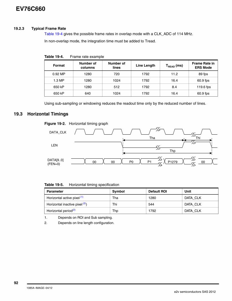
EV76C660
19.2.3 Typical Frame RateTable 19-4 gives the possible frame rates in overlap mode with a CLK_ADC of 114 MHz.
In non-overlap mode, the integration time must be added to Tread.
Using sub-sampling or windowing reduces the readout time only by the reduced number of lines.
19.3 Horizontal Timings
Figure 19-2. Horizontal timing graph
Table 19-4. Frame rate example
FormatNumber of columns
Number of lines
Line Length TREAD (ms)Frame Rate in
ERS Mode
0.92 MP 1280 720 1792 11.2 89 fps
1.3 MP 1280 1024 1792 16.4 60.9 fps
650 kP 1280 512 1792 8.4 119.6 fps
650 kP 640 1024 1792 16.4 60.9 fps
Table 19-5. Horizontal timing specification
Parameter Symbol Default ROI Unit
Horizontal active pixel (1)
1. Depends on ROI and Sub sampling.
Tha 1280 DATA_CLK
Horizontal inactive pixel (2))
2. Depends on line length configuration.
Thi 544 DATA_CLK
Horizontal period(2) Thp 1792 DATA_CLK
P0 P1 P1279
DATA_CLK
LEN
DATA[9..0] (FEN=0)
Tha
Thp
00 00 00
Thi
921085A–IMAGE–04/12
e2v semiconductors SAS 2012
EV76C660
19.4 Line_length CalculationThe sensor runs properly if the line length is currently programmed. The following paragraph gives theuser a procedure to calculate the minimum line length value to program for correct sensor operation.Line length is calculated in number of CLK_CTRL period.
If the line length is not correct, two flags can warn the user:
• The error_ll_vs_conv flag in the register h3E. A too long conversion time will set this flag.
• The error_ll_vs_xfer flag in the register h3E. A too long data readout time will set this flag.
The user must verify both to avoid any line length programming errors.
The minimum line length value to be programmed in the SPI register (@ h04) is given by the followingformula in decimal:
For a 4T pixel timing:
For a 5T pixel timing:
Table 19-6. Registers used for Line Length calculation
Entries Register Address Comments
CLK_CTRL (MHz) -
See Section 14.CLK_ADC (MHz) -
CLK_CHAIN (MHz) -
Pixtime_read_5T_width h49 Range [0;255]
Pixtime_read_4T_width h49 Range [0;255]
Max_offset h06 Range [0;255]
Roi_width Calculated in Section 4.5.3
line_length min = max [line_length_conv, line_length_roi]
8
line_length_conv = 4 + 2 × pixtime_read_4T_width +(max_offset + 210 + 40) × CLK_CTRL
CLK_ADC
line_length_roi = ROI_width × CLK_CTRL 40 × CLK_CTRLCLK_CHAIN CLK_ADC
+
line_length_conv = 4 + 2 × pixtime_read_5T_width +(max_offset + 210 + 40) × CLK_CTRL
CLK_ADC
line_length_roi = ROI_width × CLK_CTRL 40 × CLK_CTRLCLK_CHAIN CLK_ADC
+
931085A–IMAGE–04/12
e2v semiconductors SAS 2012
EV76C660
19.5 Pixel Timings
Figure 19-3. Data and sync timing diagram
19.6 FLO (Flash Strobe Output)This signal can be used to control the light source. Several SPI registers are used to define this signal.
This signal may be inverted sync_flo_inv in <reg_miscel2> see Section 17.3.4 (in the timings FLO isshown non inverted)
The FLO control mode can be selected using roi_flash_mode in <reg_ctrl_cfg> see Section 17.3.8
• FLO signal may be stuck at 1 or at 0 roi_flash_mode = h3 or h0 respectively.
• FLO1 can be calculated based on integration time only roi_flash_mode = h1
• FLO2 can be calculated based on integration time plus readout time roi_flash_mode = h2
The timings can be adjusted using t_flash_del_off and t_flash_del_on in <reg_flash_delay> seeSection 17.3.2
Programming the FLO depends on the selected mode.
Table 19-7. Data and sync timing parameters
Parameter Definition Symbol Min Typ Max Unit
Clock period Tcp 8.33 8.77 200 ns
Clock low time (1)
1. Including the clock input duty cycle 50 +/- 10% and frequency precision.Setup times: Tsd = Tcl - Tcd max - Tr / Tss = Tcl - Tcs max - TrHold times: Thd = Tch - Tcd min - Tr / Ths = Tch - Tcs min - Tr
Tcl 3.7 ns
Clock high time(1) Tch 2 ns
DATA_CLK to data Tcd -0.9 -0.2 +0.7 ns
DATA_CLK to synch FEN or LEN
Tcs -1.4 -0.6 +0.2 ns
Falling and rising edges on all signals with 10 pF load
Tr / Tf 0.8 1.5 2.6 ns
DATA_CLK
DATA[9..0]
Tsd
Tcl
Tcp
Thd Tcd
Tr Tf
Tch
FEN, LEN
Tcs Tss Ths
941085A–IMAGE–04/12
e2v semiconductors SAS 2012
EV76C660
19.6.1 FLO in GS ModeIn this mode use only the FLO based on integration time only . (FLO1)
Figure 19-4. FLO timing, serial mode GS
Figure 19-5. FLO timing, overlap mode GS
19.6.2 FLO in 4T + GR ModeIn this mode the FLO based on integration time only should be used. (FLO1). The Flash strobe should beswitched off before readout.
Figure 19-6. FLO timing, 4T + GR mode
Integration Readout
Trigger
FLO 1
t_flash_del_offt_flash_del_on
Integration
Readout
Trigger
FLO 1
t_flash_del_offt_flash_del_on
Integration Readout
Trigger
FLO 1
t_flash_del_offt_flash_del_on
951085A–IMAGE–04/12
e2v semiconductors SAS 2012
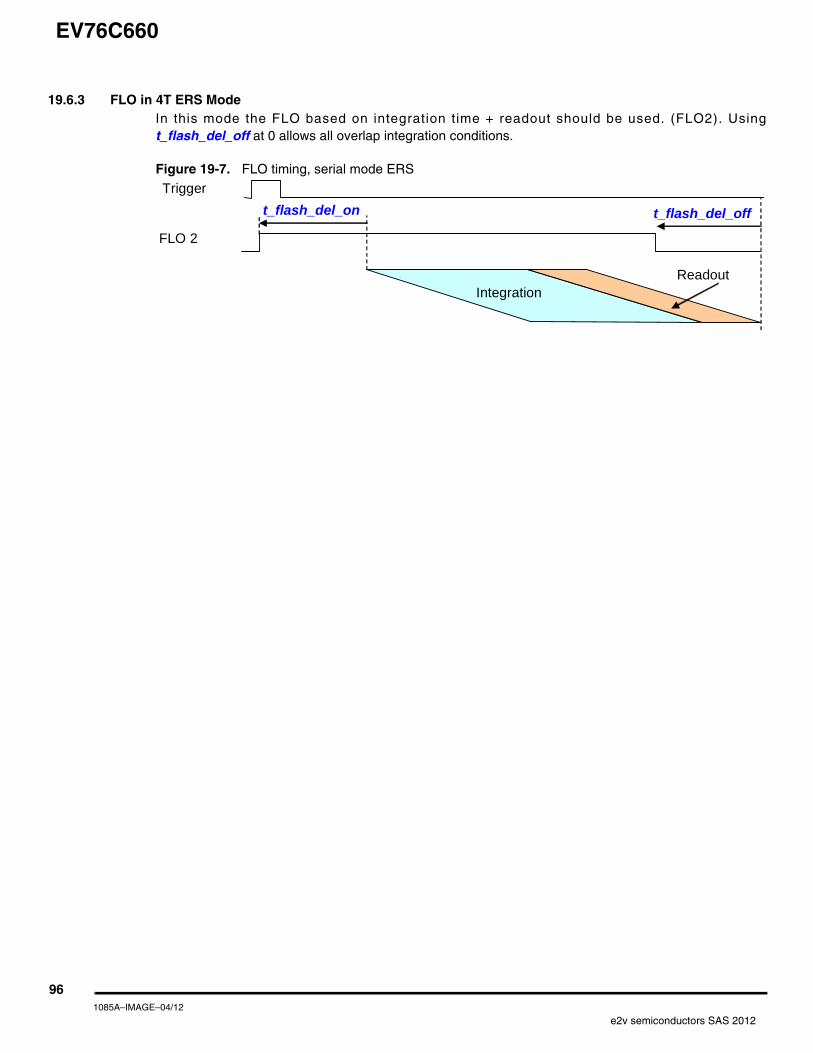
EV76C660
19.6.3 FLO in 4T ERS ModeIn this mode the FLO based on integration time + readout should be used. (FLO2). Usingt_flash_del_off at 0 allows all overlap integration conditions.
Figure 19-7. FLO timing, serial mode ERS
Integration Readout
Trigger
FLO 2
t_flash_del_offt_flash_del_on
961085A–IMAGE–04/12
e2v semiconductors SAS 2012
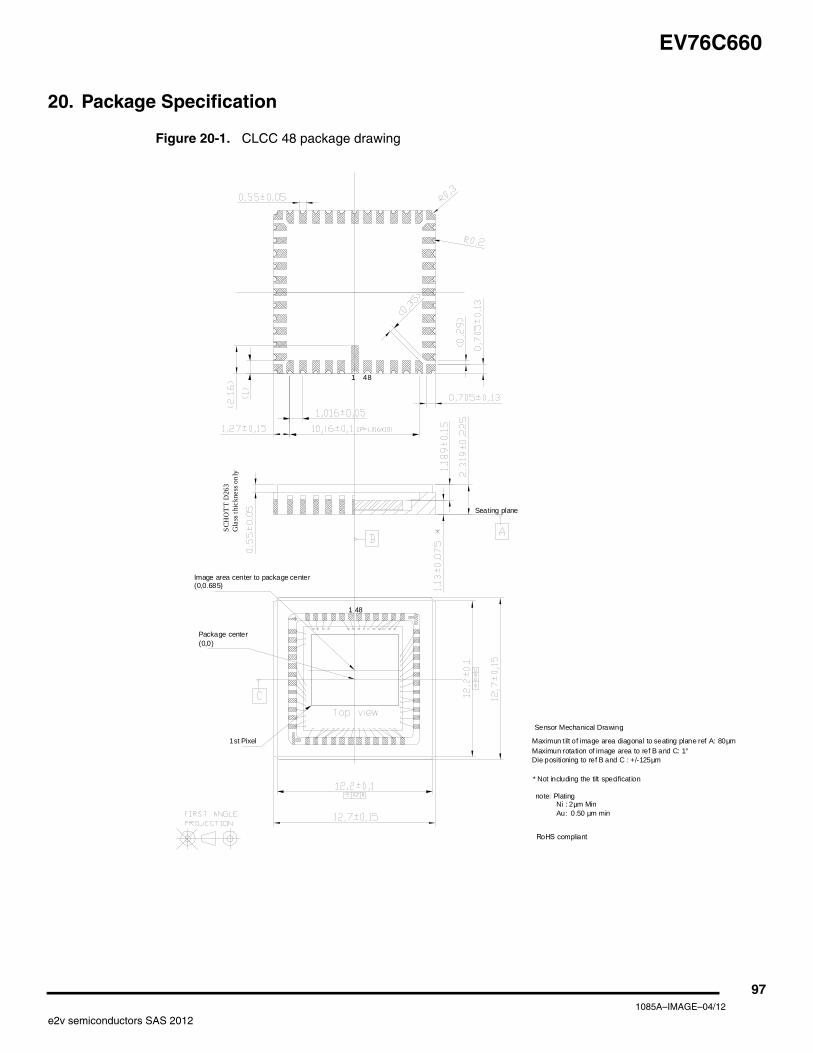
EV76C660
20. Package Specification
Figure 20-1. CLCC 48 package drawing
RoHS compliant
Maximun t ilt of image area diagonal to seating plane ref A: 80µmMaximun rotation of image area to ref B and C: 1°Die positioning to ref B and C : +/-125µm
* Not including the tilt specificat ion
note: PlatingNi : 2µm MinAu: 0.50 µm min
SCH
OT
T D
263
Gla
ss th
ickn
ess o
nly
Seating plane
Image area center to package center(0,0.685)
1st Pixel
Package center(0,0)
1 48
1 48
Sensor Mechanical Drawing
971085A–IMAGE–04/12
e2v semiconductors SAS 2012
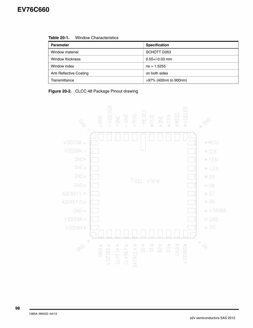
EV76C660
Figure 20-2. CLCC 48 Package Pinout drawing
Table 20-1. Window Characteristics
Parameter Specification
Window material SCHOTT D263
Window thickness 0.55+/-0.03 mm
Window index ne = 1.5255
Anti Reflective Coating on both sides
Transmittance >97% (400nm to 900nm)
981085A–IMAGE–04/12
e2v semiconductors SAS 2012
EV76C660
21. Input/Output List
Table 21-1. I/O list
Name Function / Description I/O Pin N°
VDD33A 3.3 V supply voltage for analog domain POWER (1)
1. All power pins with the same name must be connected to the same power supply
5, 8, 17
VDD18A 1.8 V Analog power, decoupling POWER(1) 9, 18
VDD18D 1.8 V supply voltage for digital domain POWER(1) 21, 30, 34, 44
GND Grounds POWER (2)
2. All grounds must be connected.
3, 7, 13, 16, 19, 20, 29, 33, 43
Test Test pins DNC(3) 10, 11, 12, 47
RESETN Reset control IN 1
TRIG Trigger input with pull-down IN 2
VREFP_1 VREFP supply for matrix DNC (3)
3. DNC stands for Do Not Connect
4
VREFP_2 VREFP supply for line decoder DNC(3) 6
ADC_REF_1 Adjusts ADC range by inserting a resistor between these two pins.
IN/OUT 14
ADC_REF_2 IN/OUT 15
CLK_FIX Clock input fixed IN 22
CLK_REF Reference Clock input IN 23
DATA_CLK Data output clock OUT 24
DATA 0 Data 0 OUT 25
DATA 1 Data 1 OUT 26
DATA 2 Data 2 OUT 27
DATA 3 Data 3 OUT 28
DATA 4 Data 4 OUT 31
DATA 5 Data 5 OUT 32
DATA 6 Data 6 OUT 35
DATA 7 Data 7 OUT 36
DATA 8 Data 8 OUT 37
DATA 9 Data 9 OUT 38
LEN Line ENable OUT 39
FEN Frame ENable OUT 40
SCK SPI Clock input IN 41
MOSI SPI Data Input in slave mode, IN 42
MISO SPI Data Output in slave mode, OUT 45
CSN SPI Chip Select Enable IN 46
FLO Flash Strobe Output OUT 48
991085A–IMAGE–04/12
e2v semiconductors SAS 2012
EV76C660
22. Document Conventions and Acronyms
22.1 SPI Register and Bitfield NamesSPI registers and bitfield names are shown in blue bold italics as follows:
example_reg_name for the entire register
example_bitfield_name in < example_reg_name> for part of the register
22.2 Numbering ConventionsHexadecimal numbers are prefixed by “h”.
In register descriptions, decimal numbers are prefixed by “d”.
Table 22-1. Glossary of acronyms
B&W Black and white
CDS Correlated double sampling
DNC Do not connect
DSNU Dark signal non-uniformity
EMC Electro Magnetic Compatibility
ERS Electronic rolling shutter
FPN Fixed pattern noise
fps Frames per second
GR Global reset
GS Global shutter
IR Infrared
LSB Least significant bit
MIMR Multiple integration multiple ROI
MSB Most significant bit
MSL Moisture sensitivity level
PGA Programmable gain amplifier
PRNU Photo response non-uniformity
ROI Region of interest
Sat Saturation value
SIMR Single integration multiple ROI
SPI Serial peripheral interface
Tint Integration time
1001085A–IMAGE–04/12
e2v semiconductors SAS 2012
EV76C660
23. Precautions for Using the Device
23.1 Absolute Maximum Ratings
• Stresses above those listed under Absolute Maximum Ratings might cause permanent device failure. Functioning at or above these limits is not recommended.
• Exposure to absolute maximum ratings for extended periods might affect reliability.
• All power pins with the same name must be connected to the same power supply.
• All grounds must be connected.
23.2 ESDThe EV76C660 is resistant up to 2 kV (HBM). To avoid accumulation of charges and to prevent electricalfield formation, the following precautions must be taken during manipulation:
• Wear anti-static gloves or finger cots, anti-static clothes and shoes.
• Protect workstation with a conductive ground sheet.
• Use conductive boxes.
23.3 Cleaning the WindowThe EV76C660 sensor is an optical device. All precautions must be taken to prevent dust or scratcheson the input window. If the window needs to be cleaned, use the procedure described here.
23.3.1 Equipment
• Ethanol.
• Cleaning medium (wipes, optical paper, cotton buds).
• Filtered blow-off gun (preferably with static charge neutralizing capability).
• Area protected from electrostatic discharges and equipped with ground straps.
23.3.2 Preparations
• Wear vinyl gloves or finger cots without talcum powder.
• Make use of anti-ESD equipment: ground straps, ionizers etc.
23.3.3 Recommendations
• Never clean with a dry cleaning medium.
• Soak the cleaning medium with alcohol and do not pour it directly on the window.
• Clean the window only if necessary.
Table 23-1. Absolute maximum ratings
Parameter Value
VDD18D digital supply voltage -0.25 V; 2.2 V
VDD18A analog supply voltage -0.25 V; 2.2 V
VDD33A analog supply voltage -0.25 V; 4 V
DC voltage at any input pin -0.25 V; VDD18D +0.25 V
Storage temperature -40°C to + 85°C
Operating temperature -30°C to + 65°C
1011085A–IMAGE–04/12
e2v semiconductors SAS 2012
EV76C660
23.3.4 Operating Procedure
• Clean the glass window with an air-jet (using the blow-off gun).
• If stains or dust remain;
– Soak the cleaning medium with alcohol and wipe the glass window in a single movement from one side to another.
– Always use a clean part of the cleaning medium for each new attempt.
– Adapt the speed of the wiping action to let alcohol evaporate without leaving traces.
– Optionally, use the blow-off gun to clean the window once more.
24. Standards ComplianceThe EV76C660 sensor conforms to the following standards:
• RoHS compliant
• Product qualification according to JEDEC JESD47
• MSL 3 compliant
25. Ordering Codes• EV76C660ABT-EQTR for monochrome product
• EV76C660ACT-EQTR for Bayer product
For other packaging or other CFA please contact e2v.
The sensors are delivered in Jedec trays
1021085A–IMAGE–04/12
e2v semiconductors SAS 2012
EV76C660
Table of Contents
1 Typical Performance Data ....................................................................... 2
2 Sensor Overview ...................................................................................... 3
3 Standard Configuration ........................................................................... 4
3.1 Sensor Settings .................................................................................................4
3.2 Application Information ......................................................................................5
3.3 Electrical Levels .................................................................................................6
4 Matrix ........................................................................................................ 7
4.1 Useful Area Definition ........................................................................................7
4.2 CFA (Color Filter Array) .....................................................................................8
4.3 Pixels .................................................................................................................8
4.4 Lens CRA (Chief Ray Angle) compensation. ....................................................8
4.5 Region Of Interest (ROI) ..................................................................................10
5 10-Bit ADC .............................................................................................. 20
5.1 Analog Gain .....................................................................................................20
5.2 External Resistor Choice .................................................................................20
5.3 Analog Gain Tolerances ..................................................................................20
6 Clamp and Offset Adjustment .............................................................. 20
7 Digital Gain ............................................................................................. 23
8 Defective Pixel Correction .................................................................... 23
9 Binning ................................................................................................... 24
10 Histograms ............................................................................................. 25
11 10 to 8-Bit Compression ....................................................................... 26
12 Context ................................................................................................... 27
13 Mux Out .................................................................................................. 29
14 Timing Generator and Power Management ......................................... 29
15 Clock Generator ..................................................................................... 30
15.1 PLL ..................................................................................................................31
15.2 Internal Oscillator .............................................................................................33
15.3 Nominal Clock Configurations .........................................................................34
i1085A–IMAGE–04/12
e2v semiconductors SAS 2012
EV76C660
16 Test Pattern Generator .......................................................................... 34
16.1 Moving Test Pattern ........................................................................................35
16.2 Fixed Test Pattern ...........................................................................................36
16.3 Functional Test Pattern ...................................................................................36
17 SPI ........................................................................................................... 37
17.1 Register Summary Tables ...............................................................................37
17.2 8-Bit Register Descriptions ..............................................................................43
17.3 16-Bit Register Descriptions ............................................................................45
17.4 SPI Timing .......................................................................................................78
18 Sensor States ......................................................................................... 80
18.1 Static States ....................................................................................................80
18.2 Active States ....................................................................................................81
18.3 Interrupt Functions ...........................................................................................87
19 Synchronization Pulse and Timings .................................................... 89
19.1 Clock Limits .....................................................................................................89
19.2 Vertical Timings ...............................................................................................90
19.3 Horizontal Timings ...........................................................................................92
19.4 Line_length Calculation ...................................................................................93
19.5 Pixel Timings ...................................................................................................94
19.6 FLO (Flash Strobe Output) ..............................................................................94
20 Package Specification ........................................................................... 97
21 Input/Output List .................................................................................... 99
22 Document Conventions and Acronyms ............................................ 100
22.1 SPI Register and Bitfield Names ...................................................................100
22.2 Numbering Conventions ................................................................................100
23 Precautions for Using the Device ...................................................... 101
23.1 Absolute Maximum Ratings ...........................................................................101
23.2 ESD ...............................................................................................................101
23.3 Cleaning the Window .....................................................................................101
24 Standards Compliance ........................................................................ 102
25 Ordering Codes .................................................................................... 102
ii1085A–IMAGE–04/12
e2v semiconductors SAS 2012

1085A–IMAGE–04/12e2v semiconductors SAS 2012
Whilst e2v has taken care to ensure the accuracy of the information contained herein it accepts no responsibility for the consequences of any usethereof and also reserves the right to change the specification of goods without notice. e2v accepts no liability beyond that set out in its standardconditions of sale in respect of infringement of third party patents arising from the use of tubes or other devices in accordance with informationcontained herein.
How to reach usHome page: www.e2v.com
Sales offices:
Europe Regional sales office
e2v ltd
106 Waterhouse Lane
Chelmsford Essex CM1 2QU
England
Tel: +44 (0)1245 493493
Fax:: +44 (0)1245 492492
E-Mail: [email protected]
e2v sas
16 Burospace
F-91572 Bièvres Cedex
France
Tel: +33 (0) 16019 5500
Fax: +33 (0) 16019 5529
E-Mail: [email protected]
e2v gmbh
Industriestraße 29
82194 Gröbenzell
Germany
Tel: +49 (0) 8142 41057-0
Fax:: +49 (0) 8142 284547
E-Mail: [email protected]
Americas
e2v inc
520 White Plains Road
Suite 450 Tarrytown NY 10591
USA
Tel: +1 (914) 592 6050 or 1-800-342-5338,
Fax:: +1 (914) 592-5148
E-Mail: [email protected]
Asia Pacific
e2v ltd
11/F.,
Onfem Tower,
29 Wyndham Street,
Central, Hong Kong
Tel: +852 3679 364 8/9
Fax: +852 3583 1084
E-Mail: [email protected]
Product Contact:
e2v
Avenue de Rochepleine
BP 123 - 38521 Saint-Egrève Cedex
France
Tel: +33 (0)4 76 58 30 00
Hotline:
Related Documents