CheironSchool_Sept2012_Lec1.ppt EUV and Soft X-Ray Optics David Attwood University of California, Berkeley Cheiron School September 2012 SPring-8 1

Welcome message from author
This document is posted to help you gain knowledge. Please leave a comment to let me know what you think about it! Share it to your friends and learn new things together.
Transcript
CheironSchool_Sept2012_Lec1.ppt
EUV and Soft X-Ray Optics
David AttwoodUniversity of California, Berkeley
Cheiron SchoolSeptember 2012SPring-8
1
CheironSchool_Sept2012_Lec1.ppt
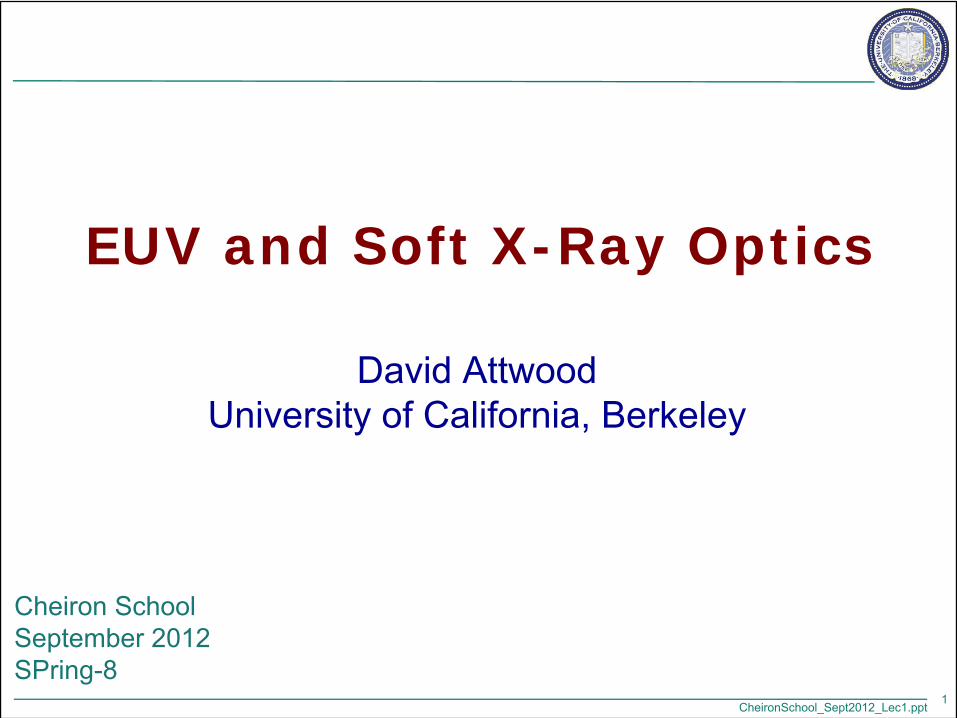
The short wavelength region of the electromagnetic spectrum
2
n = 1 – δ + iβ δ, β << 1
CheironSchool_Sept2012_Lec1.ppt
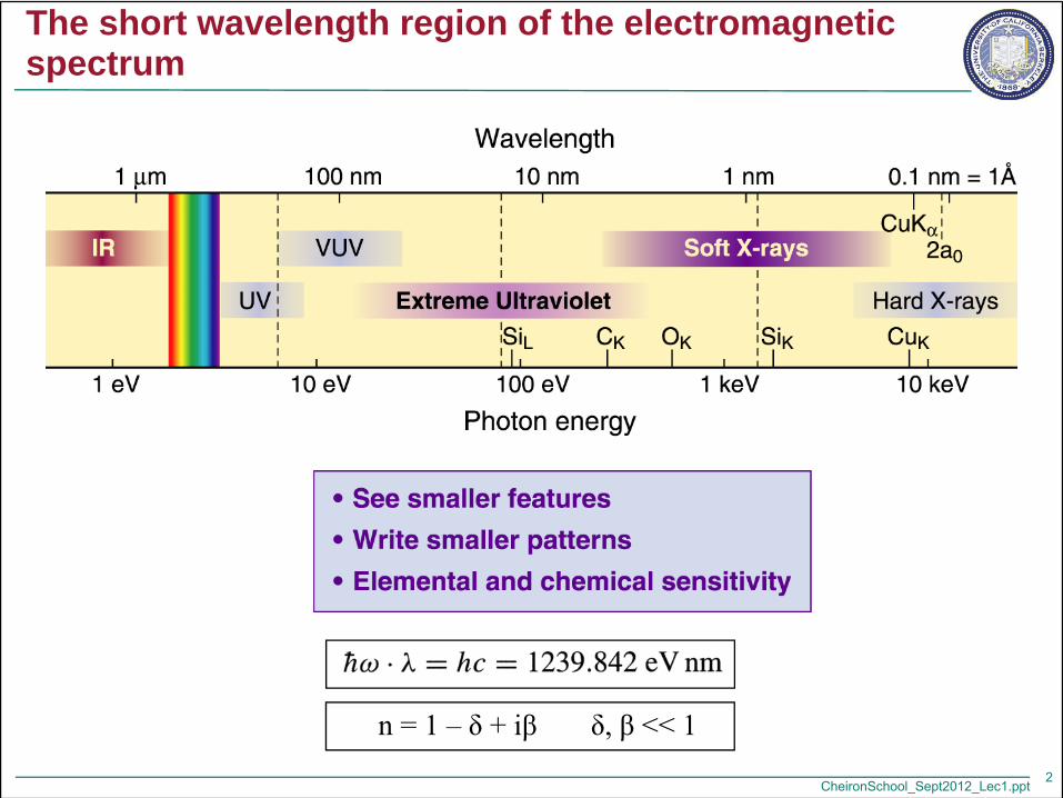
Available x-ray optical techniques
3

CheironSchool_Sept2012_Lec1.ppt
Basic ionization and emission processes in isolated atoms
4
CheironSchool_Sept2012_Lec1.ppt
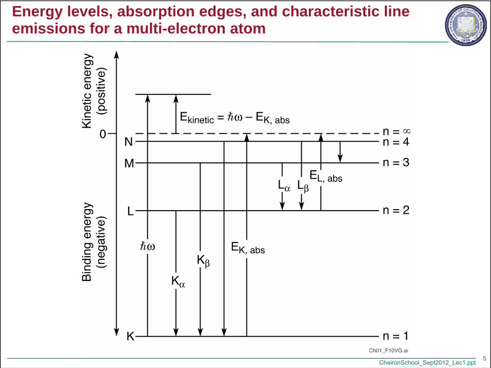
Energy levels, absorption edges, and characteristic line emissions for a multi-electron atom
5
CheironSchool_Sept2012_Lec1.ppt
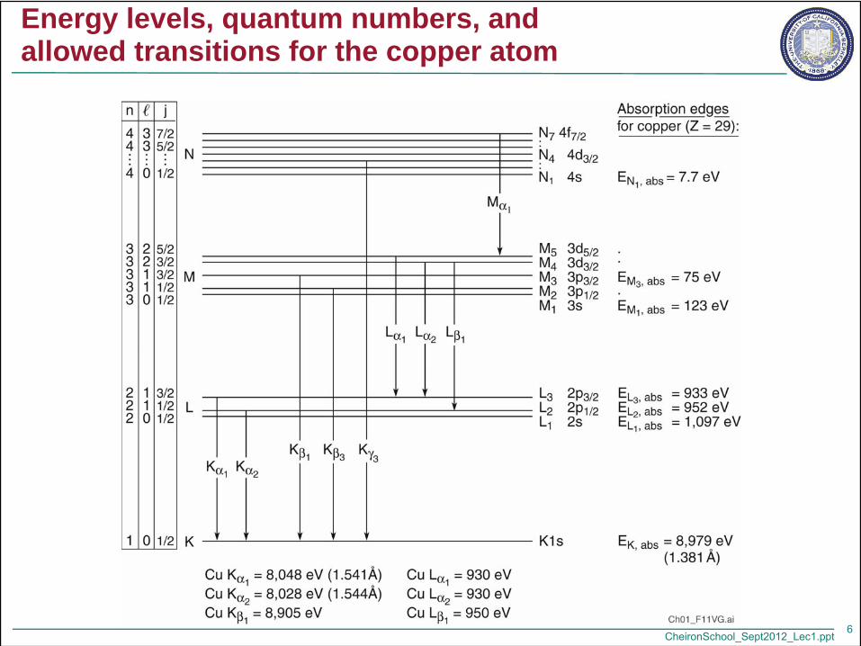
Energy levels, quantum numbers, and allowed transitions for the copper atom
6

CheironSchool_Sept2012_Lec1.ppt
Refractive index from the IR to x-ray spectral region
7
CheironSchool_Sept2012_Lec1.ppt
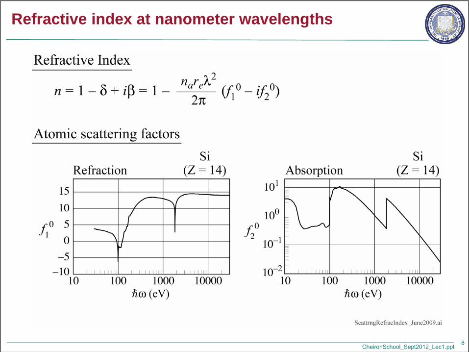
Refractive index at nanometer wavelengths
8
CheironSchool_Sept2012_Lec1.ppt
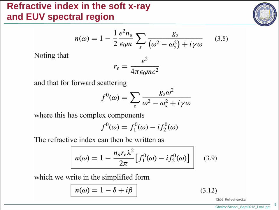
Refractive index in the soft x-rayand EUV spectral region
9
CheironSchool_Sept2012_Lec1.ppt
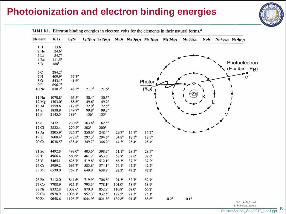
Photoionization and electron binding energies
10

CheironSchool_Sept2012_Lec1.ppt
Available x-ray optical techniques
11
CheironSchool_Sept2012_Lec1.ppt
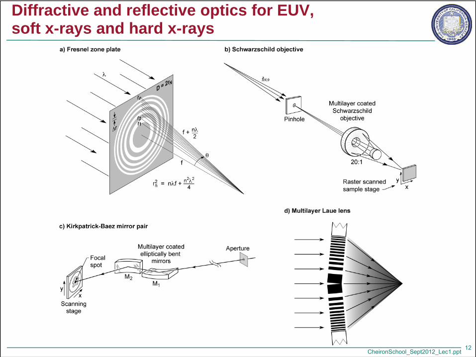
Diffractive and reflective optics for EUV, soft x-rays and hard x-rays
12
CheironSchool_Sept2012_Lec1.ppt
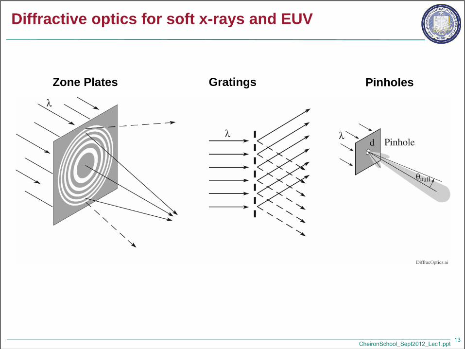
Diffractive optics for soft x-rays and EUV
13
Zone Plates Gratings Pinholes

CheironSchool_Sept2012_Lec1.ppt
Diffraction from a transmission grating
14
CheironSchool_Sept2012_Lec1.ppt
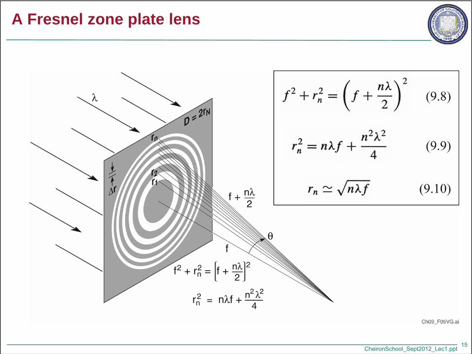
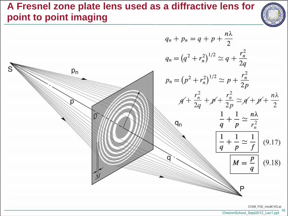
A Fresnel zone plate lens
15
CheironSchool_Sept2012_Lec1.ppt
A Fresnel zone plate lens used as a diffractive lens for point to point imaging
16
CheironSchool_Sept2012_Lec1.ppt
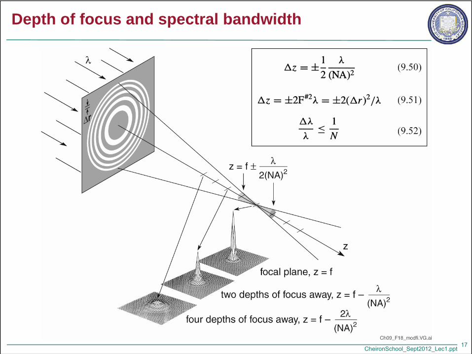
Depth of focus and spectral bandwidth
17

CheironSchool_Sept2012_Lec1.ppt
A Fresnel zone plate lensfor soft x-ray microscopy
Courtesy of E. Anderson, LBNL
18
CheironSchool_Sept2012_Lec1.ppt
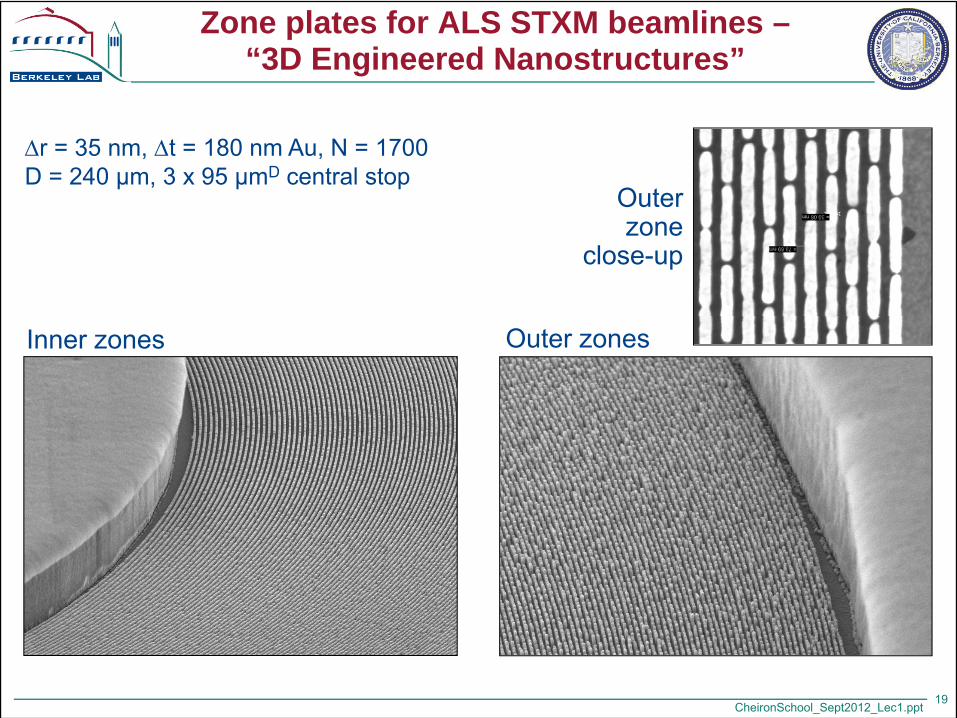
Zone plates for ALS STXM beamlines –“3D Engineered Nanostructures”
19
Δr = 35 nm, Δt = 180 nm Au, N = 1700D = 240 µm, 3 x 95 µmD central stop
Inner zones Outer zones
Outerzone
close-up
CheironSchool_Sept2012_Lec1.ppt
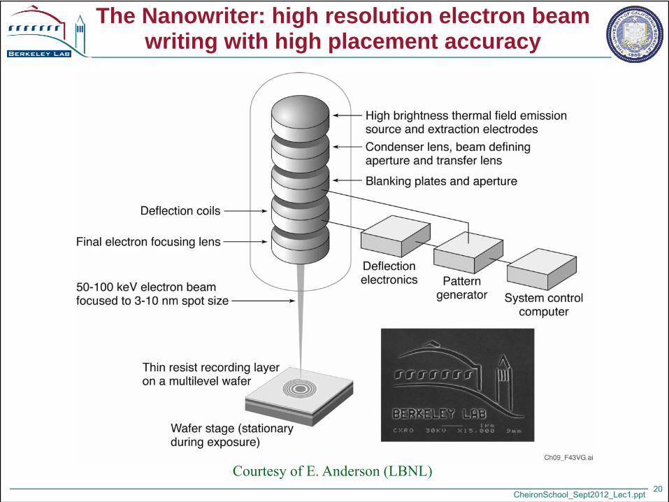
The Nanowriter: high resolution electron beam writing with high placement accuracy
20
Courtesy of E. Anderson (LBNL)
CheironSchool_Sept2012_Lec1.ppt
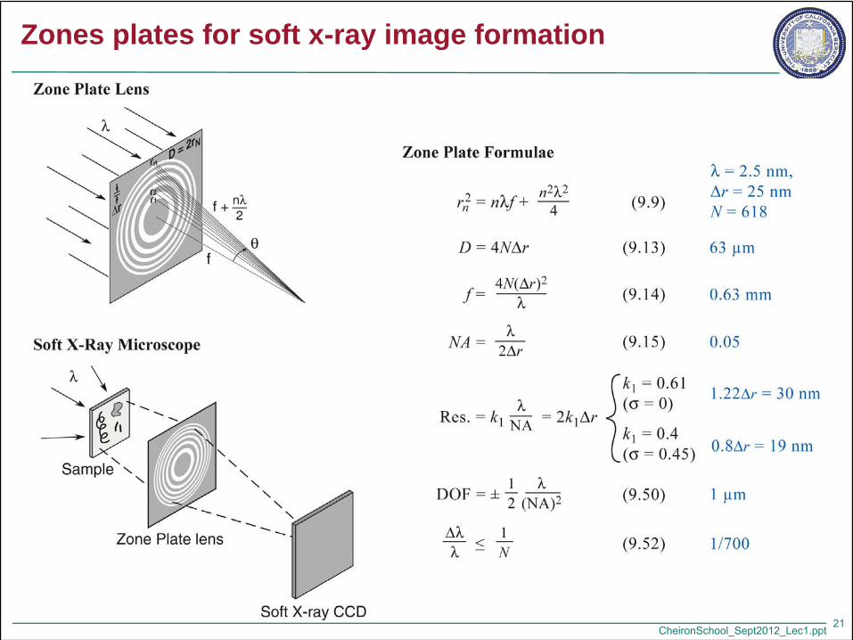
Zones plates for soft x-ray image formation
21
CheironSchool_Sept2012_Lec1.ppt
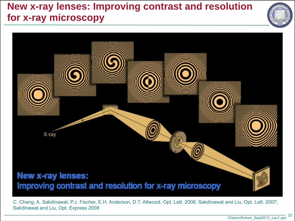
New x-ray lenses: Improving contrast and resolution for x-ray microscopy
22
C. Chang, A. Sakdinawat, P.J. Fischer, E.H. Anderson, D.T. Attwood, Opt. Lett. 2006; Sakdinawat and Liu, Opt. Lett. 2007; Sakdinawat and Liu, Opt. Express 2008
CheironSchool_Sept2012_Lec1.ppt23
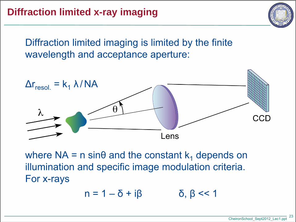
Diffraction limited imaging is limited by the finite wavelength and acceptance aperture:
Δrresol. = k1 λ / NA
where NA = n sinθ and the constant k1 depends on illumination and specific image modulation criteria.For x-rays
n = 1 – δ + iβ δ, β << 1
Diffraction limited x-ray imaging
CheironSchool_Sept2012_Lec1.ppt
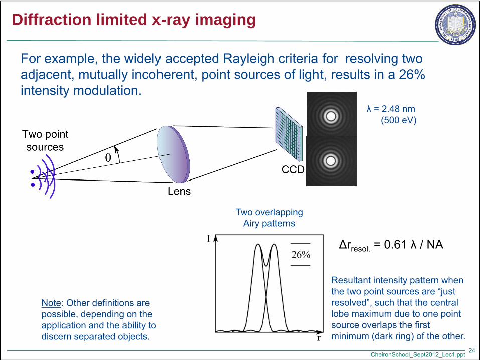
Diffraction limited x-ray imaging
For example, the widely accepted Rayleigh criteria for resolving two adjacent, mutually incoherent, point sources of light, results in a 26% intensity modulation.
24
Resultant intensity pattern when the two point sources are “just resolved”, such that the central lobe maximum due to one point source overlaps the first minimum (dark ring) of the other.
Note: Other definitions are possible, depending on the application and the ability to discern separated objects.
Two overlappingAiry patterns
λ = 2.48 nm(500 eV)
Δrresol. = 0.61 λ / NA
CheironSchool_Sept2012_Lec1.ppt
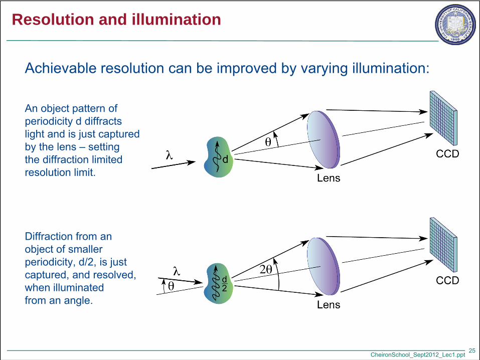
Resolution and illumination
Achievable resolution can be improved by varying illumination:
An object pattern ofperiodicity d diffractslight and is just capturedby the lens – setting the diffraction limitedresolution limit.
Diffraction from an object of smaller periodicity, d/2, is just captured, and resolved, when illuminated from an angle.
25
CheironSchool_Sept2012_Lec1.ppt
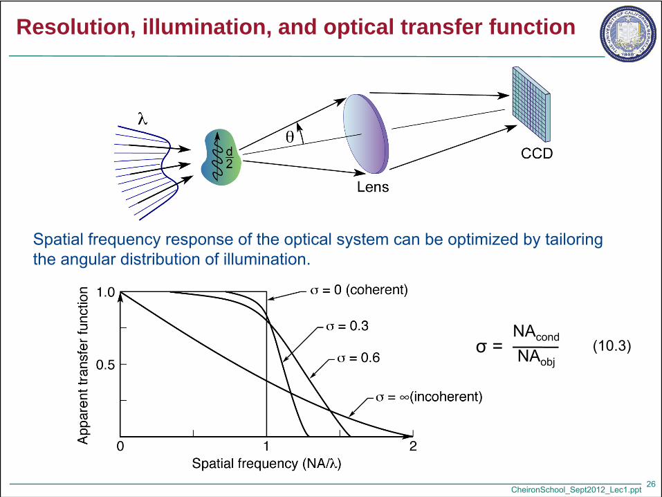
Resolution, illumination, and optical transfer function
Spatial frequency response of the optical system can be optimized by tailoring the angular distribution of illumination.
26
σ =NAcond
NAobj(10.3)
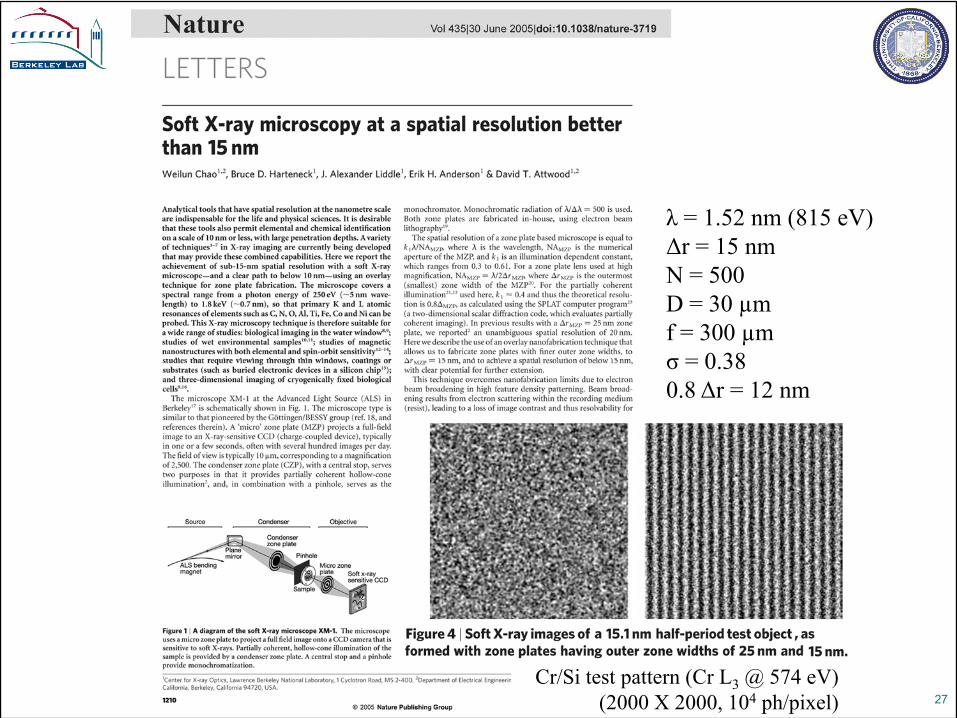
CheironSchool_Sept2012_Lec1.ppt27
λ = 1.52 nm (815 eV)Δr = 15 nmN = 500D = 30 µmf = 300 µmσ = 0.380.8 Δr = 12 nm
Cr/Si test pattern (Cr L3 @ 574 eV)(2000 X 2000, 104 ph/pixel)
CheironSchool_Sept2012_Lec1.ppt
Hard x-ray zone plate microscopy
• Shorter wavelengths, potentially better spatial resolution and greater depth-of-field.
• Less absorption (β); phase shift (δ) dominates, higher efficiency.
• Thicker structures required (e.g., zones), higher aspect ratios pose nanofabrication challenges.
• Contrast of nanoscale samples minimal; will require good statistics, uniform background, dose mitigation.
28

X-ray Zone-plate Lens
Nanoscale hard x-ray tomography
Challenges for achieving nm scale resolution: • High resolution objective lens: limiting the ultimate resolution• High numerical aperture condenser lens: • Detector: high efficiency for lab. source and high speed for synchrotron sources• Precision mechanical system
Courtesy of Wenbing Yun and Michael Feser, Xradia 29
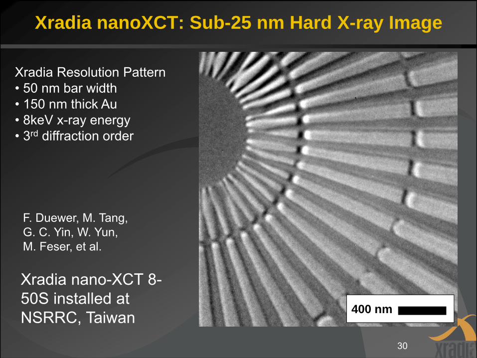
Xradia nanoXCT: Sub-25 nm Hard X-ray Image
Xradia Resolution Pattern• 50 nm bar width • 150 nm thick Au• 8keV x-ray energy• 3rd diffraction order
F. Duewer, M. Tang, G. C. Yin, W. Yun, M. Feser, et al.
Xradia nano-XCT 8-50S installed at NSRRC, Taiwan 400 nm
30

CheironSchool_Sept2012_Lec1.ppt
Hard x-ray imaging based on glancing incidence reflective optics
31
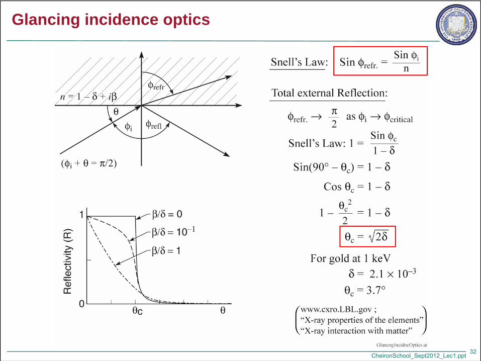
• Optics behave differently at these very short wavelengths (nanometers rather than 520 nm green light)
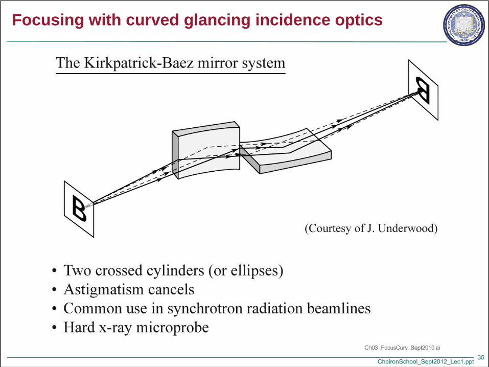
• The refractive index is less than unity, n = 1 – δ + iβ• Waves bend away form the normal at an interface• Absorption is significant in all materials and at all wavelength.• Because of absorption, refractive lenses do not work, prisms do
not, windows need to be extremely thin (100 nm or less).• Because light is bent away from the surface normal, it possible to
have “total external reflection” at glancing incidence – a commonly used technique.
• Kirkpatrick-Baez (KB)mirror pair
CheironSchool_Sept2012_Lec1.ppt
Glancing incidence optics
32
CheironSchool_Sept2012_Lec1.ppt
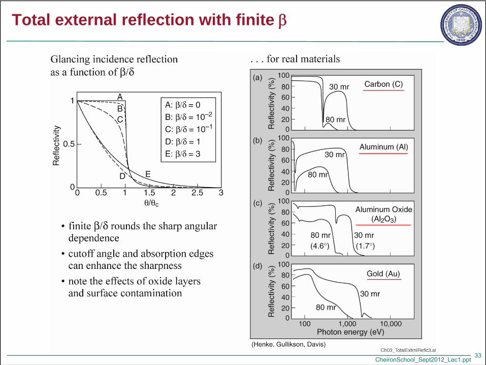
Total external reflection with finite β
33
CheironSchool_Sept2012_Lec1.ppt
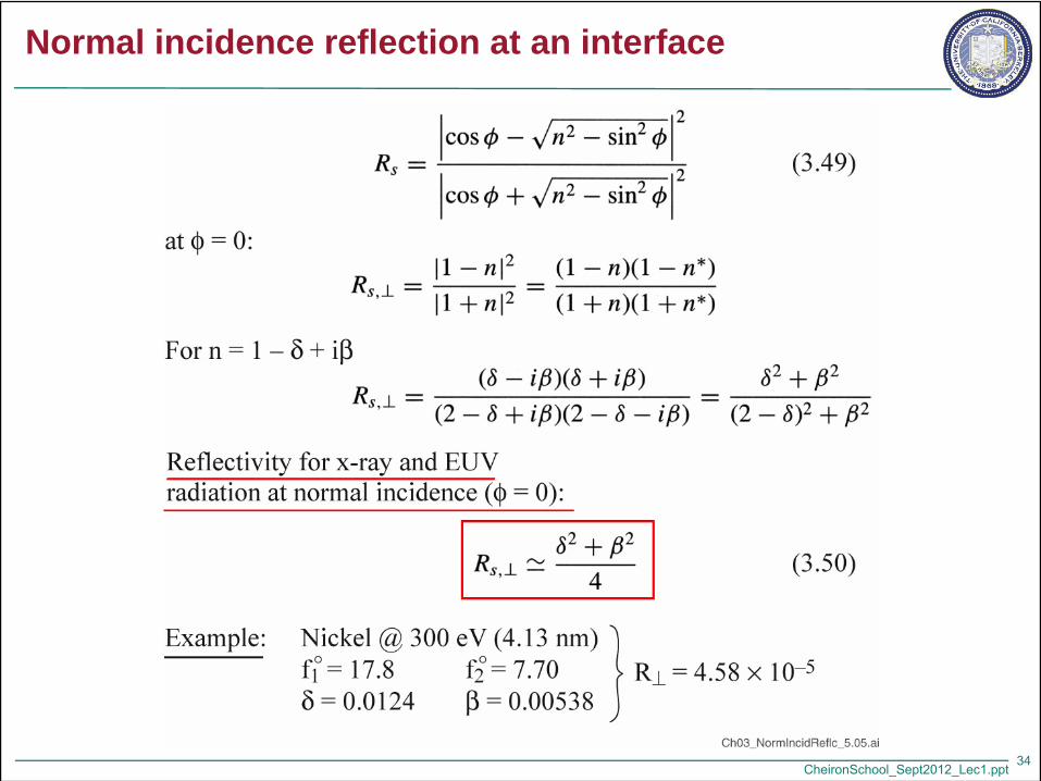
Normal incidence reflection at an interface
34
CheironSchool_Sept2012_Lec1.ppt
Focusing with curved glancing incidence optics
35
CheironSchool_Sept2012_Lec1.ppt
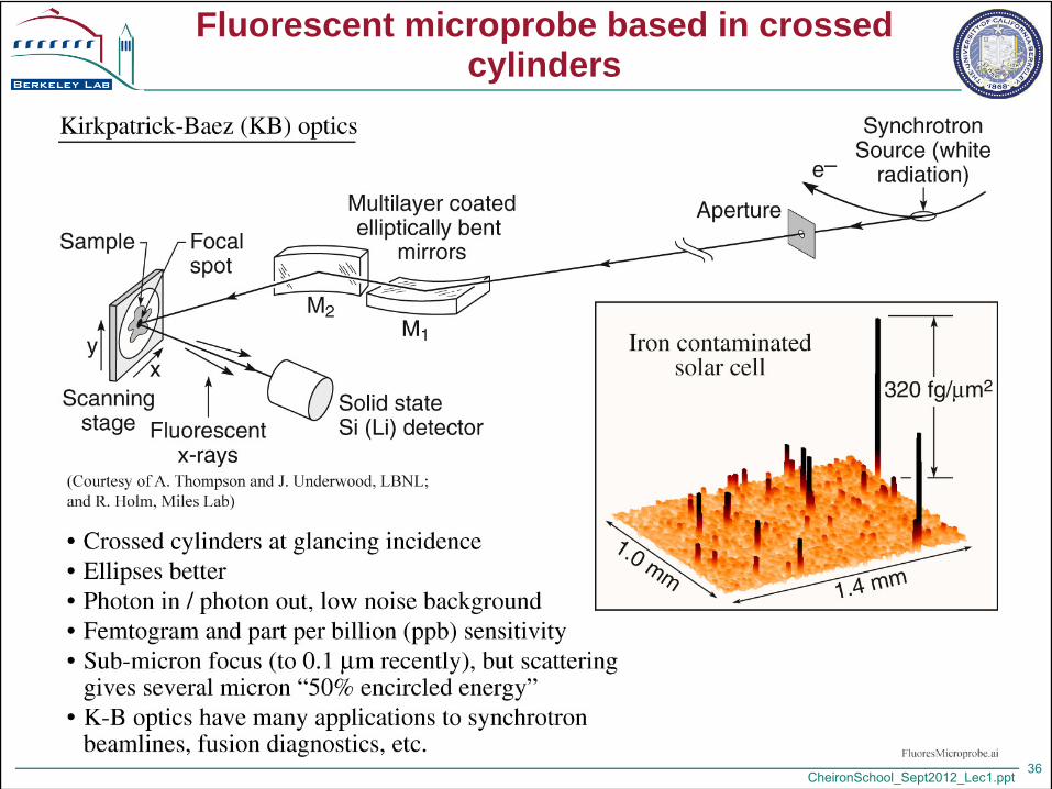
Fluorescent microprobe based in crossed cylinders
36

CheironSchool_Sept2012_Lec1.ppt
High resolution x-ray diffraction under high pressure using multilayer coated focusing optics
37
CheironSchool_Sept2012_Lec1.ppt
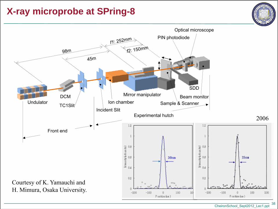
X-ray microprobe at SPring-8
38
UndulatorDCM
TC1SlitIncident Slit
Ion chamberMirror manipulator
SDD
Sample & Scanner
PIN photodiode
Beam monitor
Optical microscope
Front end
Experimental hutch
Courtesy of K. Yamauchi andH. Mimura, Osaka University.
2006
CheironSchool_Sept2012_Lec1.ppt
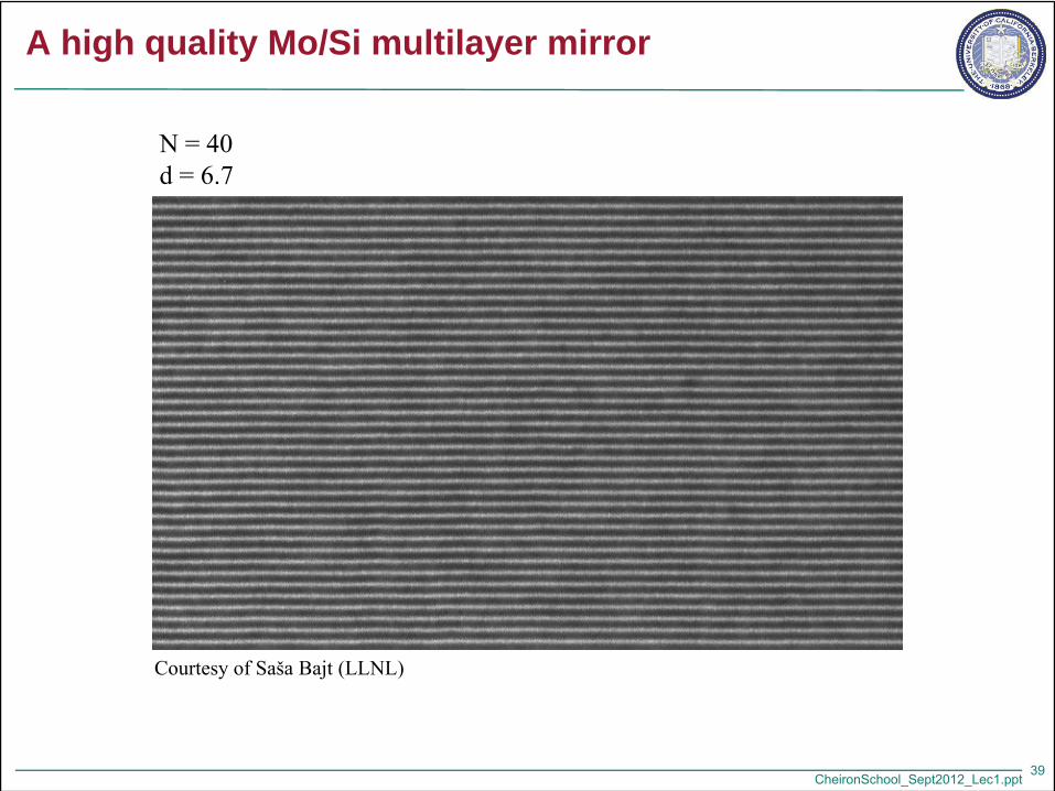
A high quality Mo/Si multilayer mirror
39
N = 40d = 6.7
Courtesy of Sasa Bajt (LLNL)ˇ
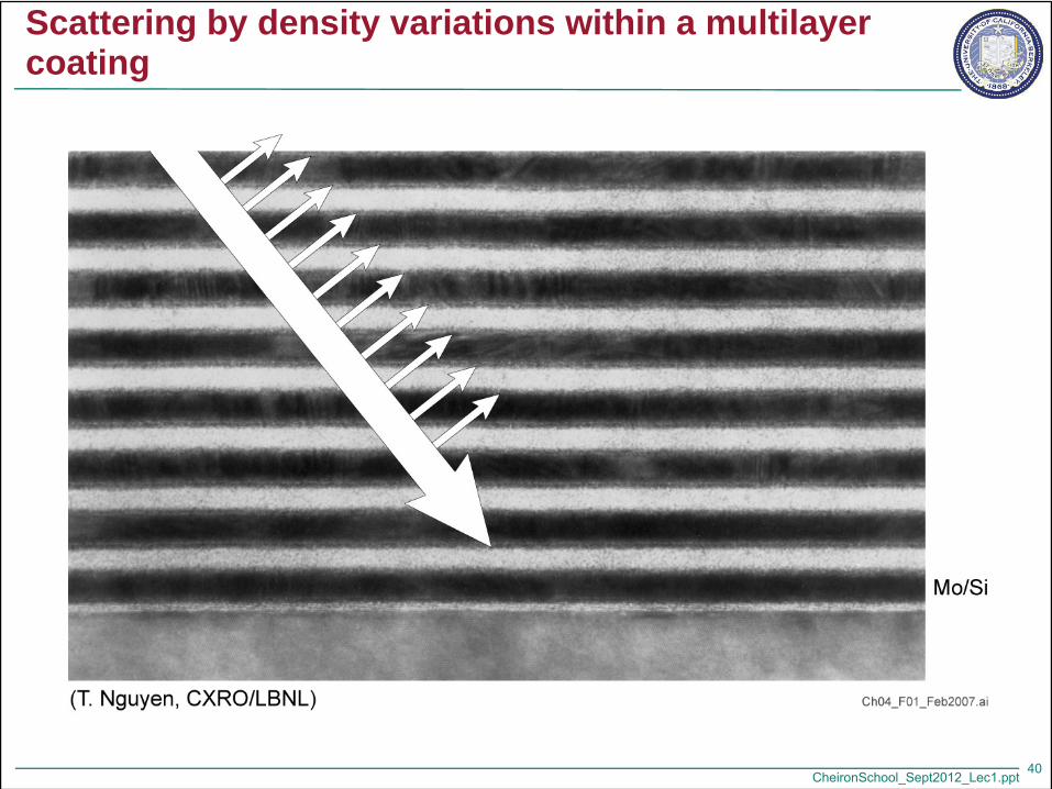
CheironSchool_Sept2012_Lec1.ppt
Scattering by density variations within a multilayer coating
40

CheironSchool_Sept2012_Lec1.ppt
Multilayer mirrors satisfy the Bragg condition
41
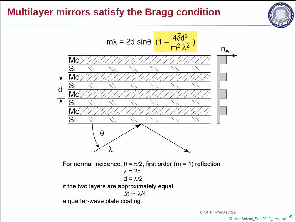
CheironSchool_Sept2012_Lec1.ppt
Multilayer mirrors satisfy the Bragg condition
42
CheironSchool_Sept2012_Lec1.ppt
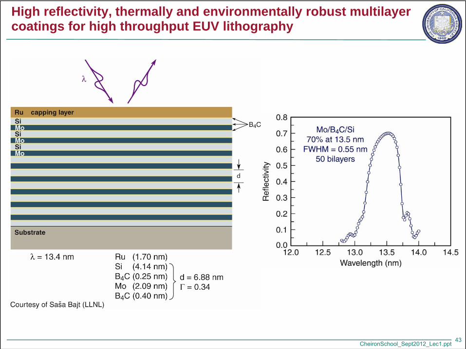
High reflectivity, thermally and environmentally robust multilayer coatings for high throughput EUV lithography
43

CheironSchool_Sept2012_Lec1.ppt
Atomic scattering factors for silicon (Z = 14)
44

CheironSchool_Sept2012_Lec1.ppt
Atomic scattering factors for molybdenum (Z = 42)
45
CheironSchool_Sept2012_Lec1.ppt
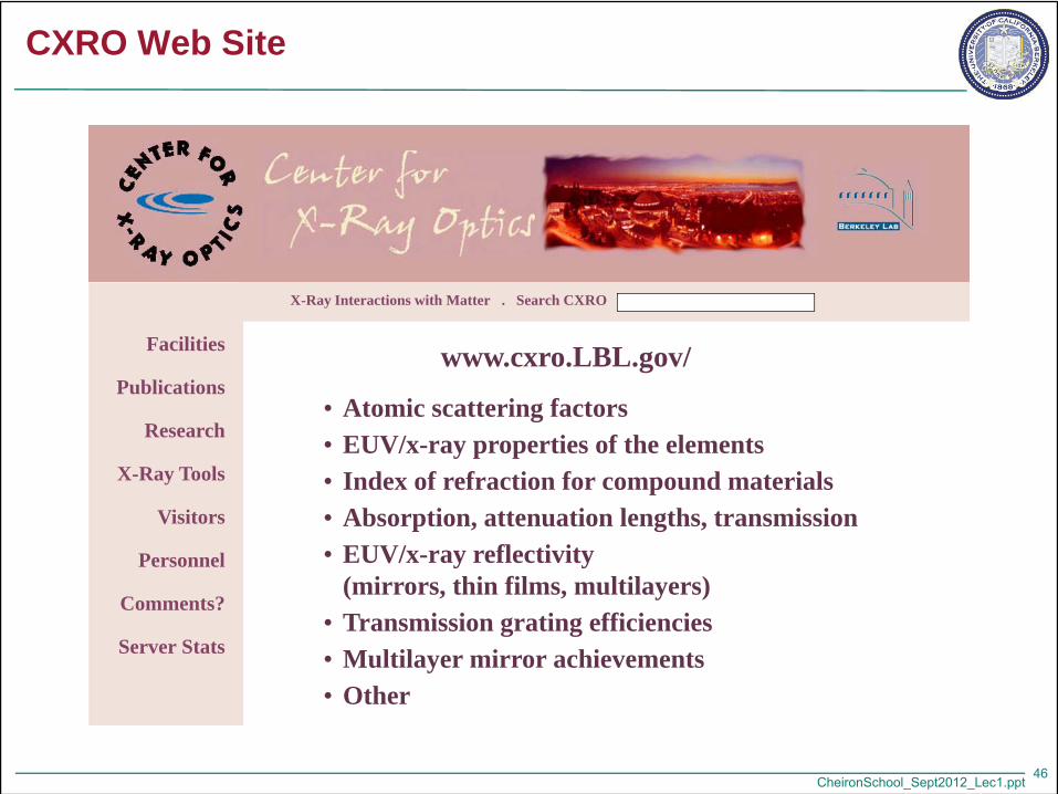
CXRO Web Site
Facilities
Publications
Research
X-Ray Tools
Visitors
Personnel
Comments?
Server Stats
X-Ray Interactions with Matter . Search CXRO . About CXRO
www.cxro.LBL.gov/
• Atomic scattering factors• EUV/x-ray properties of the elements• Index of refraction for compound materials• Absorption, attenuation lengths, transmission• EUV/x-ray reflectivity
(mirrors, thin films, multilayers)• Transmission grating efficiencies• Multilayer mirror achievements• Other
46
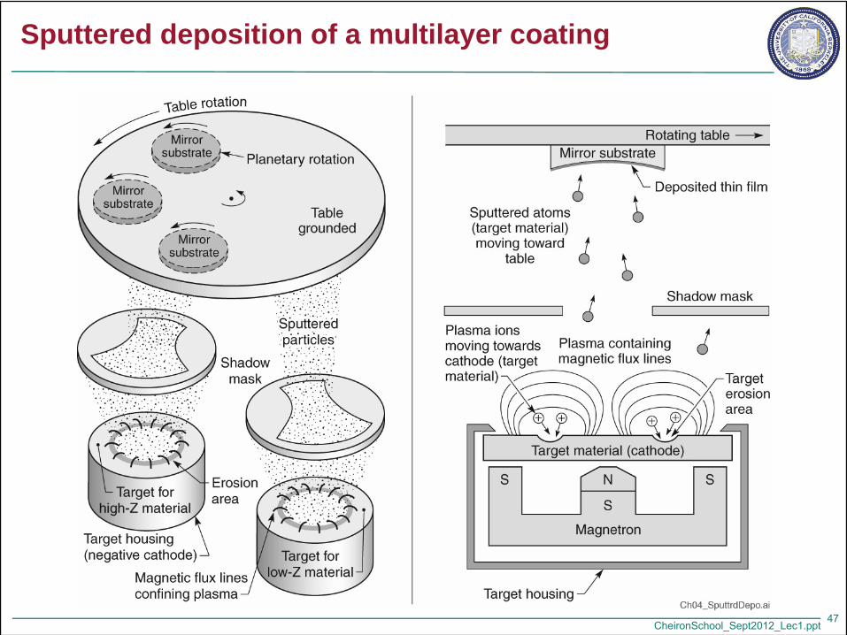
CheironSchool_Sept2012_Lec1.ppt
Sputtered deposition of a multilayer coating
47
CheironSchool_Sept2012_Lec1.ppt
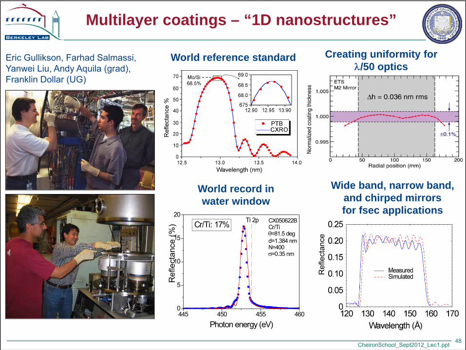
Multilayer coatings – “1D nanostructures”
48
445 450 455 4600
5
10
15
20Cr/Ti: 17% CX050622B
Cr/Tiθ=81.5 degd=1.384 nmN=400σ=0.35 nm
Ti 2p
Ref
lect
ance
(%)
Photon energy (eV)R
efle
ctan
ce
World reference standard Creating uniformity for λ/50 optics
World record in water window
Wide band, narrow band, and chirped mirrors for fsec applications
Eric Gullikson, Farhad Salmassi,Yanwei Liu, Andy Aquila (grad),Franklin Dollar (UG)

CheironSchool_Sept2012_Lec1.ppt
Broad bandwidth mirrors needed for as/fs pulses
49
• Multilayer mirrors depend on constructive interference from individual interfaces
• Higher reflectivity needs more layers
• Bandwidth gets narrower with more layers
Attosecond pulse
Broad bandwidth
Limited number of layers
N<10 layers required for
200 as pulse (@13nm)
∆E(eV) ∙∆τ(fs) ≥ 1.8 fs∙eV (FWHM)

CheironSchool_Sept2012_Lec1.ppt
Aperiodic multilayers for asec application
50
δOptimizing multilayers for specific applications requires the use of simulation of a multilayer stack with variations in the thickness of each material in the multilayer.
Successful design of aperiodicmultilayers requires:1. EM wave in multilayer
structure2. Optimization Algorithm3. Sample preparation4. Verification
A. L. Aquila, F. Salmassi, F. Dollar, Y. Liu, and E. Gullikson, "Developments in realistic design for aperiodic Mo/Si multilayer mirrors," Opt. Express 14, 10073-10078 (2006)
CheironSchool_Sept2012_Lec1.ppt
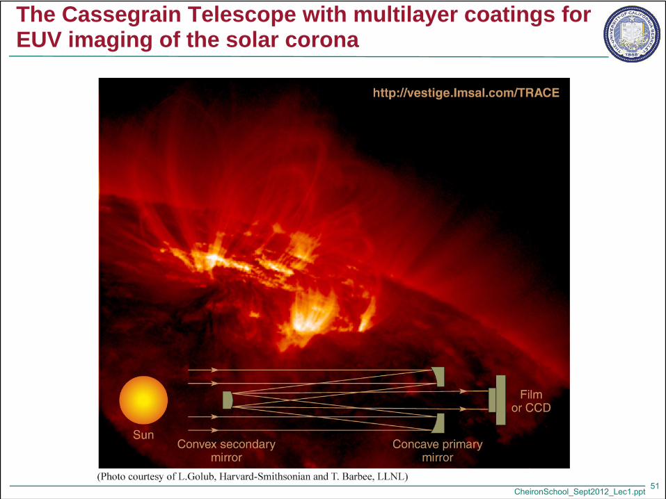
The Cassegrain Telescope with multilayer coatings for EUV imaging of the solar corona
51
CheironSchool_Sept2012_Lec1.ppt
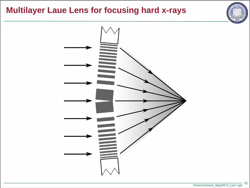
Multilayer Laue Lens for focusing hard x-rays
52
CheironSchool_Sept2012_Lec1.ppt
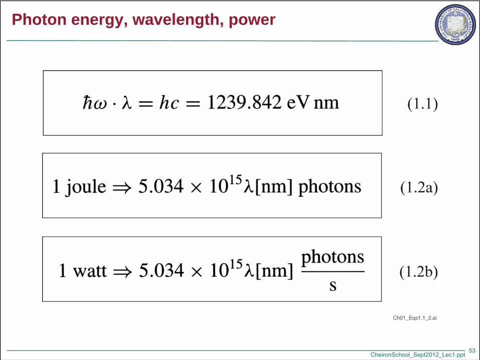
Photon energy, wavelength, power
53

CheironSchool_Sept2012_Lec1.ppt
Lectures online at www.youtube.com
Amazon.com
54
UC Berkeleywww.coe.berkeley.edu/AST/sxreuvwww.coe.berkeley.edu/AST/srms
www.coe.berkeley.edu/AST/sxr2009
Related Documents