1 RESUMEN El presente trabajo de investigación pretende mostrar el diseño de un Sistema de Control por Computadora en la Esterilización de Conservas de Pescado. El Capítulo I consta : De la justificación, objetivos generales y específicos. Como objetivo general tenemos el desarrollo y evaluación del control por computadora en la Esterilización de Conservas de Pescado y como objetivos específicos se tienen la evaluación del algoritmo de Penetración de Calor, desarrollo de las Tarjetas Acondicionadora de Señal y Adquisición de Datos y finalmente la evaluación del comportamiento del sistema mediante una simulación usando el SIMULINK ( herramienta de simulación de procesos de control retroalimentados que viene con el MATHLAB ). Luego tenemos los antecedentes, en la que mostramos los estudios y evaluaciones previas que fueron necesarios para el desarrollo de este Trabajo de Investigación. En este Trabajo no abordamos la validez del monto o cálculo de la Letalidad ( es decir la demostración de la Fórmula de Letalidad y la ecuación de Penetración de Calor ). Finalmente abordamos la descripción del problema, en donde presentamos la fórmula de Letalidad Fo y la ecuación de Penetración de Calor. En el Capítulo II presentamos el diagrama de bloques del Proceso de Esterilización y el Algoritmo de Control PID. Mostramos el Circuito completo de la Tarjeta Acondicionadora de Temperatura, de la Tarjeta de Adquisición de Datos, el Diagrama de Flujo del Algoritmo y el Programa escrito en Lenguaje C para el Control del Proceso de Esterilización de las Conservas de Pescado. El Capítulo III evaluamos el algoritmo de penetración de calor en las Conservas de Pescado y la simulación del proceso de calentamiento y enfriamiento de la Autoclave. En el Capítulo IV : Conclusiones y Recomendaciones.

Welcome message from author
This document is posted to help you gain knowledge. Please leave a comment to let me know what you think about it! Share it to your friends and learn new things together.
Transcript
1
RESUMEN
El presente trabajo de investigación pretende mostrar el diseño de un Sistema de
Control por Computadora en la Esterilización de Conservas de Pescado.
El Capítulo I consta : De la justificación, objetivos generales y específicos.
Como objetivo general tenemos el desarrollo y evaluación del control por computadora
en la Esterilización de Conservas de Pescado y como objetivos específicos se tienen la
evaluación del algoritmo de Penetración de Calor, desarrollo de las Tarjetas
Acondicionadora de Señal y Adquisición de Datos y finalmente la evaluación del
comportamiento del sistema mediante una simulación usando el SIMULINK (
herramienta de simulación de procesos de control retroalimentados que viene con el
MATHLAB ). Luego tenemos los antecedentes, en la que mostramos los estudios y
evaluaciones previas que fueron necesarios para el desarrollo de este Trabajo de
Investigación. En este Trabajo no abordamos la validez del monto o cálculo de la
Letalidad ( es decir la demostración de la Fórmula de Letalidad y la ecuación de
Penetración de Calor ). Finalmente abordamos la descripción del problema, en donde
presentamos la fórmula de Letalidad Fo y la ecuación de Penetración de Calor.
En el Capítulo II presentamos el diagrama de bloques del Proceso de
Esterilización y el Algoritmo de Control PID. Mostramos el Circuito completo de la
Tarjeta Acondicionadora de Temperatura, de la Tarjeta de Adquisición de Datos, el
Diagrama de Flujo del Algoritmo y el Programa escrito en Lenguaje C para el Control del
Proceso de Esterilización de las Conservas de Pescado.
El Capítulo III evaluamos el algoritmo de penetración de calor en las Conservas
de Pescado y la simulación del proceso de calentamiento y enfriamiento de la Autoclave.
En el Capítulo IV : Conclusiones y Recomendaciones.

2
Finalmente tenemos anexos en las cuales explicamos el principio de
funcionamiento de una termocupla y Datos Técnicos de los circuitos integrados usados en
el diseño de las Tarjetas.
3
CAPITULO I
1.1 Justificación
La presente investigación pretende estudiar la aplicación a los procesos de
tratamiento térmico de situaciones reales y simuladas de un modelo de control por
computadora. En particular, nos ceñiremos al caso de esterilización comercial de
conservas.
La industria conservera más importante del Perú tanto desde el punto de vista del
volumen de producción como de su contribución económica es la industria de conservas
de pescado, esta es la razón por la cual concentramos nuestra atención en sus especies y
productos principales. Las especies de pescado más utilizadas para enlatado de consumo
interno y exportación son la sardina (Sardinops sagax sagax) y el jurel (Trachurus
trachurus).
En los últimos años hay una tendencia a disminuir la producción de conservas de
pescado por la disponibilidad de la especia, la estacionalidad, y también a un elevado
costo de producción debido a un bajo nivel tecnológico. El costo de producción en la
esterilización de conservas de pescado está relacionado con dos variables muy
importantes : El tiempo de esterilización y consumo de energía.
Un cambio tecnológico vía el desarrollo de un control automático gobernado por
una microcomputadora sería una alternativa para bajar el costo variable en la producción
de conservas de pescado en el Perú donde los costos, además, pueden ser manejados por
el inmenso volumen de la biomasa disponible para el procesamiento.
El propósito básico para usar control automático es que la producción puede ser
lograda más económicamente, esto se lograría del siguiente modo:
4
- Disminuyendo el costo de proceso.
- Eliminando o reduciendo los errores humanos.
- Mejorando el control de calidad.
- Reduciendo el tamaño de equipos de proceso y el espacio que estos requieren.
- Proveyendo mayor seguridad en la operación.
- Minimizando el consumo de energía.
Como consecuencia de la velocidad de innovación actual de la microelectrónica, los
costos de producción y precios de venta de control de procesos tienden a bajar con el
tiempo haciéndolos asequibles a toda la industria y comunidad académica nacional.
Adicionalmente, el empleo generalizado de software en las microcomputadoras en la
construcción de modelos más realistas ha pasado de ser una preocupación estrictamente
académica a una potente herramienta del desarrollo del diseño de procesos de alimentos
en el ámbito comercial el cual está dividido en : Simulación, diseño óptimo y control.
El modelo de transferencia de calor que trabaja junto con un sistema de control
computarizado en línea en el que se obtiene la temperatura del centro de la lata en tiempo
real partiendo sólo de la temperatura de la autoclave, la que es muestreada continuamente
y leída como la temperatura de frontera a intervalos de tiempo especificados, a través de
una termocupla que siempre está disponible en todos los autoclaves comerciales. A partir
de la historia de temperatura vs. Tiempo es posible calcular la letalidad acumulada y
compararla con la letalidad de diseño del producto para controlar los tiempos de
calentamiento y enfriamiento así como responder a las desviaciones que pueden ocurrir
durante el proceso.
Finalmente, la capacidad de almacenamiento, procesamiento, así como la
versatilidad de ingresos y salidas de las nuevas familias de controladores lógicos
programables (PLC) harán posible que éste y otros modelos de control similares puedan
implementarse en conjunto con las microcomputadoras en la operación de sistemas de
5
control centralizado o distribuido para la operación simultánea de varios autoclaves y/o
otra maquinaria en una planta conservera.
1.2 Hipótesis del Trabajo
Para mejorar la productividad y el control de la calidad de la producción a nivel
industrial de conservas de pescado en el Perú, debe utilizarse el control automático por
Computadora de la Autoclave.
1.3 Objetivos
1.3.1 General
Desarrollar y evaluar un modelo para el control por computadora del procesamiento de
desmenuzado y filete de sardina, y sólidos de jurel enlatados que asegure
automáticamente la esterilización comercial en tiempo real, a pesar de desviaciones
arbitrarias en la temperatura del medio de calentamiento.
1.3.2 Específicos
- Evaluar el algoritmo de Penetración de calor.
- Desarrollar las tarjetas de acondicionamiento de señal.
- Desarrollar la tarjeta de adquisición y captura de datos.
- Evaluar mediante simulación el comportamiento del sistema.
6
1.4 Antecedentes
El modelo de penetración de calor en las conservas de pescado fue evaluado en el
año 1,994 en la Planta Piloto del I.T.P. Instituto Tecnológico Pesquero del Perú. Este
consistió en la introducción de varias termocuplas en un solo envase de conserva de
pescado para medir
Gráfico de penetración de calor en las Conservas de Pescado
Figura No. 1
Temperatura en diferentes puntos como muestra la figura. Una vez validado el modelo, se
procedió a evaluar la fórmula de Letalidad. Para esto se procedió de la siguiente forma :
- Se procedió a esterilizar las conservas de pescado a diferentes temperaturas y
tiempos, para luego realizar estudios microbiológicos de las mismas.
- Estos estudios eran el conteo de microorganismos (bacterias) remanentes y cantidad
de proteínas y vitaminas.
- Estos estudios eran para determinar las constantes de penetración de calor y tiempo
máximo de esterilización de las conservas.
7
1.5 Límites de la Investigación
Sólo deseamos construir y evaluar un modelo para conseguir la letalidad
comercial o de diseño de conservas de pescado en forma automática, no abordamos el
problema de la validez del monto o del cálculo del nivel de letalidad que necesariamente
implica la realización de estudios microbiológicos y/o físico-químicos.
1.6 Descripción del problema
1.6.1 Esterilización de Conservas de Pescado
El proceso de Esterilización de las Conservas de Pescado se realiza en grandes
hornos de esterilización. Estos hornos son grandes depósitos dentro de las cuales se llevan
en coches metálicos las latas de conservas de pescado. Una vez adentro estas latas, se abre
la válvula de vapor para aumentar la temperatura interna de la autoclave. La temperatura
interna es medida a través de un sensor de temperatura (termocupla) colocada en el
interior del horno y controlada por, valga la redundancia, un controlador de temperatura. (
Ver figura 2 adjunta en la siguiente página.)
La temperatura a la cual debe llegar es de 250 F y por un tiempo de 40 minutos aprox.
Estos valores pueden variar de proceso en proceso, dependiendo del tamaño de las latas
de conserva y la cantidad de las mismas. ¿Porqué se debe llegar a esta temperatura y
durante este tiempo ?. Se ha realizado estudios microbiológicos ( conteo de bacterias ) y
se determinó que con 250 ºF en la autoclave y durante 40 minutos se llegaría a la letalidad
( mortalidad ) de microorganismos deseada para una determinada cantidad de latas de
conservas de pescado. Es necesario realizar estos estudios ya que si por alguna razón
sobrepasamos la temperatura y/o el tiempo de calentamiento, no solo destruimos a los
8
microorganismos ( bacterias ) sino también a las proteínas y vitaminas, por lo que la
conserva quedaría inutilizada.
En todo este proceso de esterilización, de las dos variables, temperatura de la
autoclave y letalidad, únicamente la temperatura es posible medirla y controlarla en
tiempo real, mientras que la letalidad no.
De acuerdo a estudios realizados en la década de los setenta, se desarrolló algoritmos
para hallar la letalidad en enlatados. Estos algoritmos dependen de la temperatura interna
en el punto mas frío del enlatado ( normalmente en el centro geométrico del mismo ) y
está dada por la siguiente ecuación :
Fórmula de letalidad en el Centro de la Conserva de Pescado
Donde F es la letalidad, th es el tiempo de calentamiento en el centro de la lata, tc es el
tiempo de enfriamiento, Z es una constante que depende del material enlatado y T es la
temperatura en el centro de la lata.
Por lo tanto la primera integral es la contribución a la letalidad F en el proceso de
calentamiento, y la segunda integral es la contribución a la letalidad F en el proceso de
enfriamiento. Es necesario incluir la fase de enfriamiento, ya que según estudios éste
puede llegar a ser hasta 40% del valor total del F. El valor de F en la fase de enfriamiento
no puede ser despreciado, no es una constante y no puede ser controlada, por lo tanto ella
puede ser estimada antes que se inicie el proceso de enfriamiento.
Si de algún modo se pudiera obtener en tiempo real la temperatura interna de la lata
de conserva ( en el centro geométrico), entonces es posible hallar la letalidad también en
)1(10 /)250(
0
/)250(
10 ∫∫+
−−+=
ch
h
h tt
t
ZT
tZT
dtdtF
9
tiempo real. Como esta variable ( letalidad ) es un factor de diseño ( tiene un valor
determinado ), entonces es posible detener todo el proceso una vez llegado a este valor.
La fórmula usada para hallar la temperatura interna en un punto dado está dada por
ecuaciones diferenciales de transferencia de calor y es de la forma :
Ecuación Diferencial de transferencia de calor en las Conservas de Pescado
Donde T es la temperatura interna, r es la posición radial en el cilindro, h es la
posición vertical en el cilindro, t es el tiempo y a es la difusividad térmica. Por lo tanto
es posible hallar en tiempo real mediante la lectura de la temperatura de la autoclave la
letalidad de los microorganismos y compararla con el valor deseado.
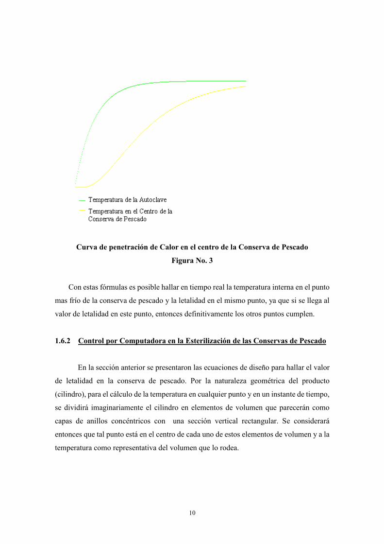
En la figura 3 podemos observar la curva de penetración en el centro de la conserva
de pescado.
)2(11
2
2
2
2
r
T
r
T
rh
T
t
T
a ∂
∂+
∂
∂+
∂
∂=
∂
∂
10
Curva de penetración de Calor en el centro de la Conserva de Pescado
Figura No. 3
Con estas fórmulas es posible hallar en tiempo real la temperatura interna en el punto
mas frío de la conserva de pescado y la letalidad en el mismo punto, ya que si se llega al
valor de letalidad en este punto, entonces definitivamente los otros puntos cumplen.
1.6.2 Control por Computadora en la Esterilización de las Conservas de Pescado
En la sección anterior se presentaron las ecuaciones de diseño para hallar el valor
de letalidad en la conserva de pescado. Por la naturaleza geométrica del producto
(cilindro), para el cálculo de la temperatura en cualquier punto y en un instante de tiempo,
se dividirá imaginariamente el cilindro en elementos de volumen que parecerán como
capas de anillos concéntricos con una sección vertical rectangular. Se considerará
entonces que tal punto está en el centro de cada uno de estos elementos de volumen y a la
temperatura como representativa del volumen que lo rodea.
11
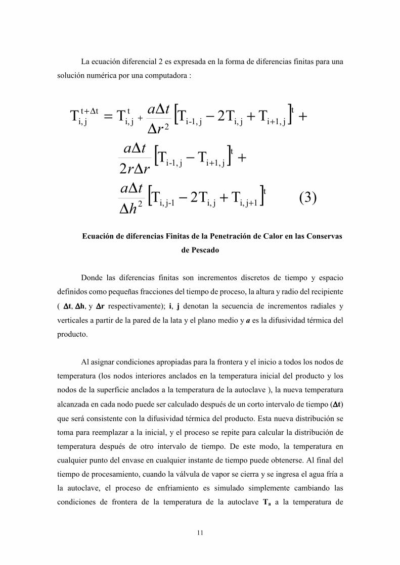
La ecuación diferencial 2 es expresada en la forma de diferencias finitas para una
solución numérica por una computadora :
Ecuación de diferencias Finitas de la Penetración de Calor en las Conservas
de Pescado
Donde las diferencias finitas son incrementos discretos de tiempo y espacio
definidos como pequeñas fracciones del tiempo de proceso, la altura y radio del recipiente
( ∆∆∆∆t, ∆∆∆∆h, y ∆∆∆∆r respectivamente); i, j denotan la secuencia de incrementos radiales y
verticales a partir de la pared de la lata y el plano medio y a es la difusividad térmica del
producto.
Al asignar condiciones apropiadas para la frontera y el inicio a todos los nodos de
temperatura (los nodos interiores anclados en la temperatura inicial del producto y los
nodos de la superficie anclados a la temperatura de la autoclave ), la nueva temperatura
alcanzada en cada nodo puede ser calculado después de un corto intervalo de tiempo (∆∆∆∆t)
que será consistente con la difusividad térmica del producto. Esta nueva distribución se
toma para reemplazar a la inicial, y el proceso se repite para calcular la distribución de
temperatura después de otro intervalo de tiempo. De este modo, la temperatura en
cualquier punto del envase en cualquier instante de tiempo puede obtenerse. Al final del
tiempo de procesamiento, cuando la válvula de vapor se cierra y se ingresa el agua fría a
la autoclave, el proceso de enfriamiento es simulado simplemente cambiando las
condiciones de frontera de la temperatura de la autoclave Ta a la temperatura de
[ ]
[ ]
[ ] )3(TT2T
TT2
TT2TTT
t
1ji,ji,1-ji,2
t
j1,ij1,-i
t
j1,iji,j1,-i2
t
ji,
tt
ji,
+
+
++∆+
+−∆
∆
+−∆
∆
++−∆
∆=
h
ta
rr
ta
r
ta
12
enfriamiento Tc en los nodos de la superficie y continuando con las iteraciones de la
computadora tal como ya se describió.
De este modo la temperatura en el centro del envase puede ser calculada después
de cada intervalo para producir la curva de penetración de calor desde la cual el valor de
esterilización del proceso F, puede ser calculado.
Como semilla para iniciar los cálculos para las iteraciones iniciaremos con 200 elementos
de volumen en el envase completo, y la temperatura en el centro de cada elemento será
calculada cada octavo de minuto (7.5 segundos)
13
CAPITULO II
ANALISIS DEL PROBLEMA
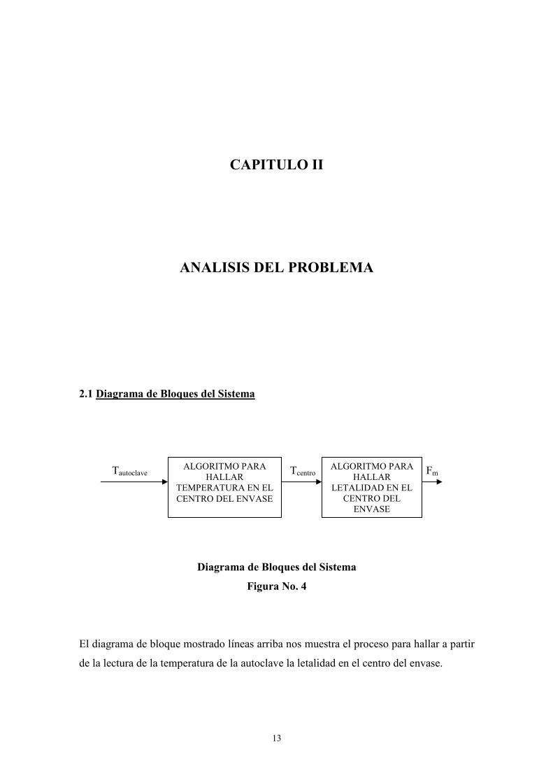
2.1 Diagrama de Bloques del Sistema
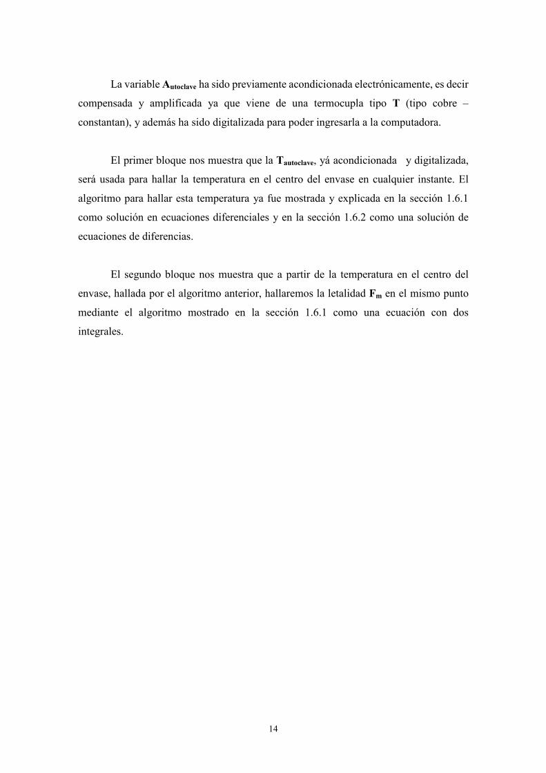
Tautoclave Tcentro Fm
Diagrama de Bloques del Sistema
Figura No. 4
El diagrama de bloque mostrado líneas arriba nos muestra el proceso para hallar a partir
de la lectura de la temperatura de la autoclave la letalidad en el centro del envase.
ALGORITMO PARA
HALLAR
TEMPERATURA EN EL
CENTRO DEL ENVASE
ALGORITMO PARA
HALLAR
LETALIDAD EN EL
CENTRO DEL
ENVASE
14
La variable Autoclave ha sido previamente acondicionada electrónicamente, es decir
compensada y amplificada ya que viene de una termocupla tipo T (tipo cobre –
constantan), y además ha sido digitalizada para poder ingresarla a la computadora.
El primer bloque nos muestra que la Tautoclave, yá acondicionada y digitalizada,
será usada para hallar la temperatura en el centro del envase en cualquier instante. El
algoritmo para hallar esta temperatura ya fue mostrada y explicada en la sección 1.6.1
como solución en ecuaciones diferenciales y en la sección 1.6.2 como una solución de
ecuaciones de diferencias.
El segundo bloque nos muestra que a partir de la temperatura en el centro del
envase, hallada por el algoritmo anterior, hallaremos la letalidad Fm en el mismo punto
mediante el algoritmo mostrado en la sección 1.6.1 como una ecuación con dos
integrales.
15
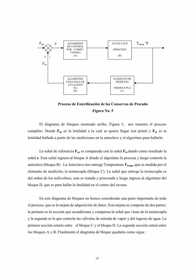
Fsp e Ttemp oF
+ -
Fm
Proceso de Esterilización de las Conservas de Pescado
Figura No. 5
El diagrama de bloques mostrado arriba, Figura 5, nos muestra el proceso
completo. Donde Fsp es la letalidad a la cual se quiere llegar (set point) y Fm es la
letalidad hallada a partir de las mediciones en la autoclave y el algoritmo para hallarlo.
La señal de referencia Fsp es comparada con la señal Fm dando como resultado la
señal e. Esta señal ingresa al bloque A donde el algoritmo la procesa y luego controla la
autoclave (bloque B) . La Autoclave nos entrega Temperatura Ttemp, que es medida por el
elemento de medición, la termocupla (bloque C). La señal que entrega la termocupla es
del orden de los milivoltios; esta es tratada y procesada y luego ingresa al algoritmo del
bloque D, que es para hallar la letalidad en el centro del envase.
En este diagrama de bloques no hemos considerado una parte importante de todo
el proceso, que es la tarjeta de adquisición de datos. Esta tarjeta se compone de dos partes:
la primera es la sección que acondiciona y compensa la señal que viene de la termocupla
y la segunda es la que controla las válvulas de entrada de vapor y del ingreso de agua. La
primera sección estaría entre el bloque C y el bloque D. La segunda sección estará entre
los bloques A y B. Finalmente el diagrama de bloque quedaría como sigue :
ALGORIMTO DE CONTROL
POR COMPU-
TADORA
(A)
AUTOCLAVE
(PROCESO)
(B)
ALGORITMO PARA HALLAR
LETALIDAD
F(t)
(D)
ELEMENTO DE MEDICION
TERMOCUPLA (C)
16
Fsp e TtemoF
+ -
Fm
Proceso de Esterilización de las Conservas de Pescado
Figura No. 6
Para entender mejor el proceso usando el computador como controlador de la
autoclave, El diagrama general sería :
X (s) Y (S)
COMPUTADOR
Sistema de Control basado en un Computador
Figura No. 7
La función de transferencia del diagrama de bloques mostrando líneas
arriba es como sigue:
ALGORITMO
PARA HALLAR
LETALIDAD F(t)
(D)
ELEMENTO DE
MEDICION
TERMOCUPLA
(C)
ALGORIMTO
DE CONTROL POR COMPU-
TADORA
(A)
AUTOCLAVE
(PROCESO)
(B)
CONTROL DE
VALVULAS DE AGUA Y
VAPOR
ACONDICIONADOR
Y COMPENSADOR
DE TEMPERATURA
CONTROLADOR PID
GC(S)
PLANTA
P(S)
ELEMENTO DE MEDICION
TERMOCUPLA
H(S)
17
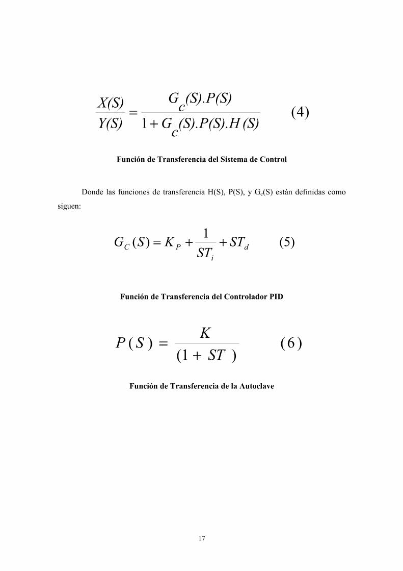
Función de Transferencia del Sistema de Control
Donde las funciones de transferencia H(S), P(S), y Gc(S) están definidas como
siguen:
Función de Transferencia del Controlador PID
Función de Transferencia de la Autoclave
)4(1 (S)(S).P(S).H
cG
(S).P(S)c
G
Y(S)
X(S)
+=
)5(1
)( d
i
PC STST
KSG ++=
)6()1(
)(ST
KSP
+=
18
Función de Transferencia de la Termocupla
Donde
Kp es la ganancia proporcional del controlador
Ti es la constante integrativa
Td es la constante derivativa
K es la temperatura de trabajo de la autoclave
KM es la sensibilidad de la termocupla tipo T.
T es el tiempo de respuesta de la autoclave
TA es el tiempo de respuesta de la termocupla
Para el desarrollo de esta investigación estamos asumiendo una función de
transferencia típica de una autoclave ya que al momento de implementar es necesario
hallar las constantes de la autoclave, así como de la termocupla.
Conociendo todas las constantes, podríamos simular el proceso de control y
validar nuestra ecuación de letalidad en el envase de conserva de pescado.
En realidad sólo es necesario la ecuación del control PID para poder usarlo como
algoritmo de control de la autoclave :
Función de Transferencia de un Controlador PID
)7(1
)(ST
KSH
A
M
+=
)8(1
)( d
i
PC STST
KSG ++=
19
e u
Diagrama de Bloques de un Controlador PID
Figura No. 8
Si nos vamos al dominio discreto, entonces según Tustin reemplazamos s :
Aproximación de Tustin
Donde GC(s) es la Función de Transferencia del controlador PID, e(s) es la señal de error
a la entrada del controlador y u(s) es la salida del controlador.
Simplificando tendremos :
[KP(Z2 - 1) + a(Z
2 + 2Z + 1) + b(Z
2 - 2Z + 1)]e(Z) = u(Z) (Z
2 - 1)
(11)
)9()1(
)1(.
2 −
+=
Z
ZTS
)10()(
)()(
Su
SeSG C =
KP
1/TiS
TdS
20
donde
dividiendo entre Z2 tenemos lo siguiente :
Z-2(KP+a+b)e(Z)+Z
-1(2a-2b)e(Z)+(KP+a+b)e(Z)+Z
-2u(Z)= u(Z)
(12)
Si tomamos como muestras discretas, tendremos :
e(K-2)(KP+a+b)+e(K-1)(2a-2b)+e(K)(KP+a+b)+u(K-2)=u(K)
(13)
Donde las muestras e(K-2), e(K-1), e(K), u(K-2) y u(K) son muestras discretas de las
señales en tiempos pasados (t-2), (t-1), (t). Por lo tanto la ecuación del control PID
depende de las muestras pasadas y presentes tanto de la entrada como de la salida.
Esta fórmula nos ayudará mucho en la construcción del algoritmo de control PID
i
d
TTb
TTa
2
2
.==
21
2.2 Tarjeta Acondicionadora de Temperatura
En la siguiente figura nos muestra el diagrama de bloques de la tarjeta
compensadora de temperatura y en la siguiente página se encuentra el esquema completa
de la Tarjeta Acondicionadora.
Termocupla
Tarjeta Acondicionadora de Temperatura
Figura No. 9
La Termocupla es conectada a los terminales VI+ y VI- donde es compensada por
R1, R2, R3, R4, R5 y D1. El potenciómetro R1 se calibra de tal modo que a la salida del
sensor de Temperatura LM335, es decir en el punto A, nos entregue en voltaje la
temperatura ambiente. Estos componentes hacen que la unión fría de la termocupla sea
compensada y la salida sea únicamente función de la temperatura de la autoclave (ver
anexo 1 Principio de Funcionamiento de las Termocuplas). Para hallar los valores
correctos de R2 y R3 debemos tener la curva o datos de temperatura vs voltaje de la
termocupla que nos debe entregar el fabricante. En la siguiente sección se explica el modo
de hallar dichos valores. A la entrada del pin 3 del OPAMP U1A tenemos el voltaje dado
por la termocupla ( del orden de los milivoltios ) referido a 0ºC más una porción de la
fuente VCC. Para eliminar este voltaje, hacemos un divisor de resistencias R12, R13, R14
y lo introducimos en el OPAMP U1B para que a la salida del Amplificador Instrumental
formado por los OPAMP´s U1A, U1B, U1C y U1D, el voltaje amplificado sea función
únicamente del voltaje de la termocupla. El uso de un Amplificador Instrumental es
debido a su elevado CMRR ( alrededor de 120 dB) lo que nos daría mayor estabilidad en
la amplificación de la señal proveniente de la termocupla.
Acondiciona-
dora de
Temperatura
Amplificador de alta
impedancia y alto CMRR
(Amplificador Instrumental)
Filtro RC
22
23
La señal ya amplificada ingresa al OPAMP U2A (pin 2), el cual es un sumador,
ajustándose el voltaje a sumar por el potenciómetro R19. A la salida de este sumador
viene un filtro activo pasa bajos formado por el OPAMP U2B para filtrar cualquier ruido
externo
La tarjeta compensadora de temperatura es externa a la computadora ya que debe
acondicionar previamente la señal de la termocupla y poder enviarla hacia la
computadora para su procesamiento. Por lo tanto esta tarjeta debe encontrarse entre la
autoclave y la computadora.
2.2.1 Calibracion de la tarjeta compensadora
Para calibrar la tarjeta compensadora de Temperatura es necesario realizar varios
pasos. El primero de ellos es que al momento de adquirir la termocupla tipo T, el
fabricante nos debe entregar la curva característica de la misma. De acuerdo a esta curva o
tabla de valores debemos hallar la sensibilidad de la termocupla para nuestro rango de
trabajo. Es muy importante hallar este valor ya que lo usamos para diseñar la sección
compensadora de unión fría de la termocupla.
Supongamos que nuestra termocupla tipo T ( Cobre-Constantan ) tiene una
sensibilidad S en [µV/° C] y es conectada a la tarjeta compensadora de Temperatura. En
el circuito mostrado en la figura 10, se observa que la termocupla es conectada junto con
otro sensor de temperatura, el LM335. Este sensor lo usamos para compensar la unión
fría de la termocupla ( ver anexo 1). La sensibilidad de este sensor es de 10 mV/°C, por lo
que hacemos un arreglo de resistencias ( R2 y R3 ) para igualar estas sensibilidades. Esto
se logra del siguiente modo :
24
Donde despejamos la relación R2/R3 y tenemos la siguiente :
Podemos asumir un valor para R3 y hallar R2. Por ejemplo si asumimos R3 = 220Ω,
entonces el valor de R2. Una vez hallado los valores de R2 y R3 procedemos a realizar los
ajustes de la tarjeta compensadora.
Lo primero que debemos hacer es ajustar la resistencia R12 (ADJUST) de tal modo que
cuando se cortocircuiten las entradas donde va conectada la termocupla, la salida del
operacional U1C nos dé 0.00 Voltios (en el punto B). Esto se hace para eliminar la
componente de voltaje DC que proviene de la fuente VCC.
Una vez hecho este ajuste, es necesario calibrar la tarjeta con la termocupla que se
va a usar. El procedimiento de calibración es el siguiente:
1) Es necesario contar con un controlador PID con una Histéresis de 1 °C, un
voltímetro, un elemento calefactor (puede ser una hornilla), y un PT100 como
elemento de medición de temperatura.
)/(32
3)/(10CmVS
RR
xRCmVVI °=
+
°=−
1)/(
)/(10
3
2−
°
°=
CmVS
CmV
R
R
25
2) En un recipiente con hielo ( 0 °C ) se sumerge completamente la termocupla y
se ajusta la resistencia R19 (ZERO) hasta que la salida del OPAMP U2B nos
indique 0.00 Voltios en el voltímetro.
3) Luego usamos el controlador, el PT 100 y la hornilla calefactora con un
recipiente semihermético para llegar a 150 °C. Conectamos la hornilla y el
sensor PT100 al controlador para formar en pequeño sistema controlado a
una temperatura de 150 °C ( tal como en la figura 11 ). Una vez que en el
interior del recipiente halla 150 °C introducimos la termocupla lo mas cerca
posible al PT100 y ajustamos con la resistencia R11 (SPAN) hasta un valor de
5.00 Voltios.
4) Luego regresamos al punto 2 para verificar y/o ajustar hasta que a la salida de
la tarjeta para 0ºC nos dé 0.00V y a 150ºC no dé 5.00V.
Como la tarjeta acondicionadora es externa a la computadora, entonces es
necesario que el cable de la termocupla llegue hasta dicha tarjeta. Por lo tanto, al realizar
la calibración de la tarjeta con la termocupla, es necesario que ésta esté conectada con el
cable que será usado en planta para que no existan errores de compensación.
PT 100
Histéresis =< 1 °C
Diagrama para la calibración de la Tarjeta Acondicionador de Temperatura
Figura 11
El tipo de cable usado para llevar la señal de la tarjeta compensadora a la
computadora es un cable enmallado multifilar para tener protección al ruido industrial
CONTROLADOR PID
SET POINT 150 °C
ELEMENTO CALEFACTOR
T = 150 ° C
26
existente. El cable coaxial no es recomendado ya que tiene espacios entre el núcleo y el
dieléctrico y esto crea capacitancias parásitas.
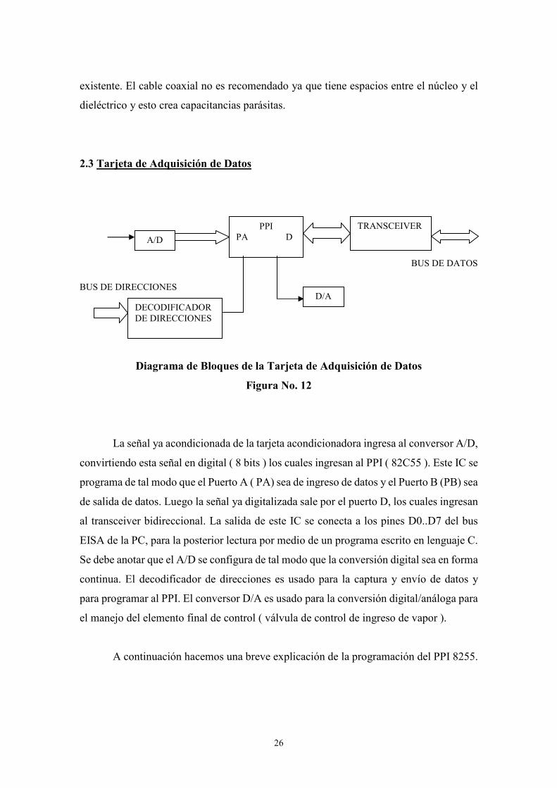
2.3 Tarjeta de Adquisición de Datos
BUS DE DATOS
BUS DE DIRECCIONES
Diagrama de Bloques de la Tarjeta de Adquisición de Datos
Figura No. 12
La señal ya acondicionada de la tarjeta acondicionadora ingresa al conversor A/D,
convirtiendo esta señal en digital ( 8 bits ) los cuales ingresan al PPI ( 82C55 ). Este IC se
programa de tal modo que el Puerto A ( PA) sea de ingreso de datos y el Puerto B (PB) sea
de salida de datos. Luego la señal ya digitalizada sale por el puerto D, los cuales ingresan
al transceiver bidireccional. La salida de este IC se conecta a los pines D0..D7 del bus
EISA de la PC, para la posterior lectura por medio de un programa escrito en lenguaje C.
Se debe anotar que el A/D se configura de tal modo que la conversión digital sea en forma
continua. El decodificador de direcciones es usado para la captura y envío de datos y
para programar al PPI. El conversor D/A es usado para la conversión digital/análoga para
el manejo del elemento final de control ( válvula de control de ingreso de vapor ).
A continuación hacemos una breve explicación de la programación del PPI 8255.
A/D
PPI
PA D
PB
D/A
DECODIFICADOR
DE DIRECCIONES
TRANSCEIVER
27
E/S PA7 - PA0
E/S PC7 - PC4
E/S PC3 - PC0
E/S PB7 - PB0
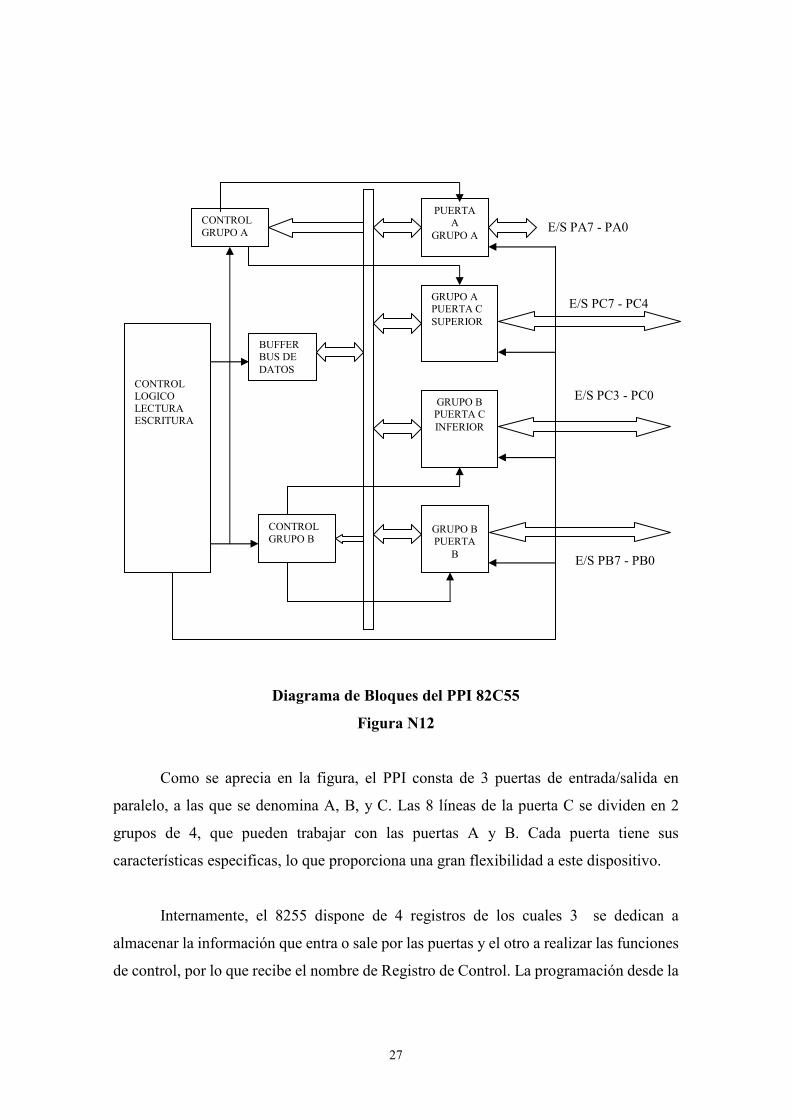
Diagrama de Bloques del PPI 82C55
Figura N12
Como se aprecia en la figura, el PPI consta de 3 puertas de entrada/salida en
paralelo, a las que se denomina A, B, y C. Las 8 líneas de la puerta C se dividen en 2
grupos de 4, que pueden trabajar con las puertas A y B. Cada puerta tiene sus
características especificas, lo que proporciona una gran flexibilidad a este dispositivo.
Internamente, el 8255 dispone de 4 registros de los cuales 3 se dedican a
almacenar la información que entra o sale por las puertas y el otro a realizar las funciones
de control, por lo que recibe el nombre de Registro de Control. La programación desde la
CONTROL
GRUPO A
PUERTA A
GRUPO A
GRUPO A PUERTA C
SUPERIOR
GRUPO B PUERTA C
INFERIOR
GRUPO B
PUERTA
B
CONTROL
GRUPO B
BUFFER BUS DE
DATOS
CONTROL
LOGICO
LECTURA ESCRITURA
28
CPU de este último registro, sirve para configurar las puertas y el funcionamiento general
del PPI.
Modos de Funcionamiento
El PPI admite 3 modos diferentes de funcionamiento, que se denominan Modo 0, Modo 1
y Modo 2.
Modo 0.
Es la forma más sencilla y básica de comportamiento de las puertas de E/S. Las 3
puertas pueden trabajar como entrada o salida, pero sin la posibilidad de disponer de
líneas auxiliares de control para soportar el dialogo con los periféricos.
Modo 1
En este caso es posible que las puertas A y B puedan dialogar con los periféricos,
actuando las líneas de la puerta C como soporte de las señales de dialogo.
Modo 2
Se permite trabajar a la puerta A de forma bidireccional, o sea que puede actuar como
entrada y salida de información, utilizando ciertas líneas de la puerta C para establecer el
diálogo con los periféricos. En este modo la puerta B puede actuar en Modo 0 o Modo 1.
Programación del Registro de Control
La palabra que se escribe en el Registro de Control del PPI configura su
funcionamiento. En la figura , se muestra la misión de cada uno de los bits que componen
29
este registro. Cuando el bit de mas peso tiene un uno, el Registro de Control determina el
modo de trabajo de las 3 puertas según los restantes bits. En el caso de que el bit de mas
peso sea un cero, los restantes bits del Registro de Control se usan para sacar 1 ó 0 por las
líneas de la puerta C.
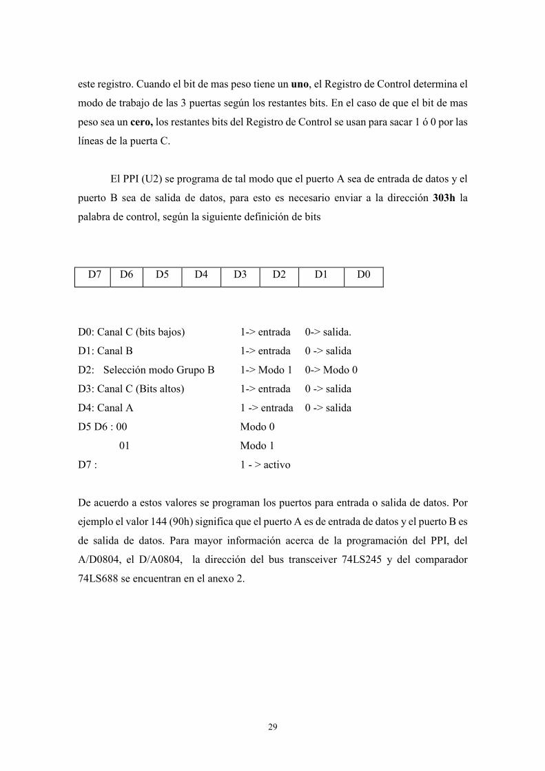
El PPI (U2) se programa de tal modo que el puerto A sea de entrada de datos y el
puerto B sea de salida de datos, para esto es necesario enviar a la dirección 303h la
palabra de control, según la siguiente definición de bits
D7 D6 D5 D4 D3 D2 D1 D0
D0: Canal C (bits bajos) 1-> entrada 0-> salida.
D1: Canal B 1-> entrada 0 -> salida
D2: Selección modo Grupo B 1-> Modo 1 0-> Modo 0
D3: Canal C (Bits altos) 1-> entrada 0 -> salida
D4: Canal A 1 -> entrada 0 -> salida
D5 D6 : 00 Modo 0
01 Modo 1
D7 : 1 - > activo
De acuerdo a estos valores se programan los puertos para entrada o salida de datos. Por
ejemplo el valor 144 (90h) significa que el puerto A es de entrada de datos y el puerto B es
de salida de datos. Para mayor información acerca de la programación del PPI, del
A/D0804, el D/A0804, la dirección del bus transceiver 74LS245 y del comparador
74LS688 se encuentran en el anexo 2.
30
31
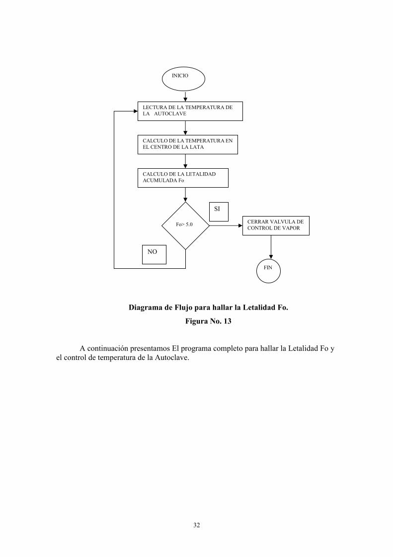
2.4 Algoritmo para hallar la Letalidad Fo
Se usó el lenguaje de programación C por ser el más conveniente para el control
por computadora. Así mismo es muy sencillo la captura y envío de datos por los puertos
de comunicación. A continuación presentamos el diagrama de flujo del programa y luego
el algoritmo.
El programa se inicia con la lectura de la Temperatura en la Autoclave. Con este
valor se calcula la temperatura en el centro de la conserva de pescado. Una vez hallado
este valor se procede a hallar el valor de la Letalidad acumulada Fo en el mismo punto
hasta ese momento. Si este valor de Letalidad Fo es mayor o igual a 5.0, entonces es
necesario cerrar las válvulas de control de ingreso de vapor y abrir las válvulas de ingreso
de agua fría. En caso que Fo ( Letalidad ) sea menor a 5.0, se procede a medir
nuevamente la temperatura de la Autoclave, calculando otra vez la temperatura
interna de la conserva de pescado y Fo ( Letalidad ).
32
Diagrama de Flujo para hallar la Letalidad Fo.
Figura No. 13
A continuación presentamos El programa completo para hallar la Letalidad Fo y
el control de temperatura de la Autoclave.
LECTURA DE LA TEMPERATURA DE
LA AUTOCLAVE
CALCULO DE LA TEMPERATURA EN
EL CENTRO DE LA LATA
CALCULO DE LA LETALIDAD
ACUMULADA Fo
Fo> 5.0 CERRAR VALVULA DE
CONTROL DE VAPOR
FIN
INICIO
SI
NO

33
Programa para hallar la Letalidad Fo y el control de la Autoclave
#include <dos.h>
#include <conio.h>
#include <graphics.h>
#include <stdio.h>
#include <stdlib.h>
#include <math.h>
#include <ctype.h>
# include <time.h>
main()
float a, dt, r, h, z, fo, dr, dh, alpha, beta, gamma, Td, Ti;
float ta, tr[6],e[6], u[6], xx, yy, zz, semilla, temp,aa, bb, Kp;
int tf[11][11][111], ti[11][11][111];
int t, y, x, i, ii, j, jj, t1, t2, ff, porta, portb, portc;
int control,temperatura;
aa = 7.5*Td/2.0;
bb = 2.0/(7.5*Ti);
temp = 240.0;
a = .85;
dt = .25;
r = 10.795;
h = 5.08;
z = 18.0;
fo = 0.0;
dr = r / 10.0;
dh = h / 10.0;
ta = 68.0;
fo = 0.0;
porta = 768;
portb = 769;
portc = 770;
control = 771;
alpha = a * dt / (dr * dr);
beta = a * dt / (2 * r * dr);
gamma = a * dt / (dh * dh);
for(t=0; t<=110; t++)
for(y=0; y<=10; y++)
for(x=0; x<=10; x++)
ti[x][y][t] = 68.0;
tf[x][y][t] = 0.0;
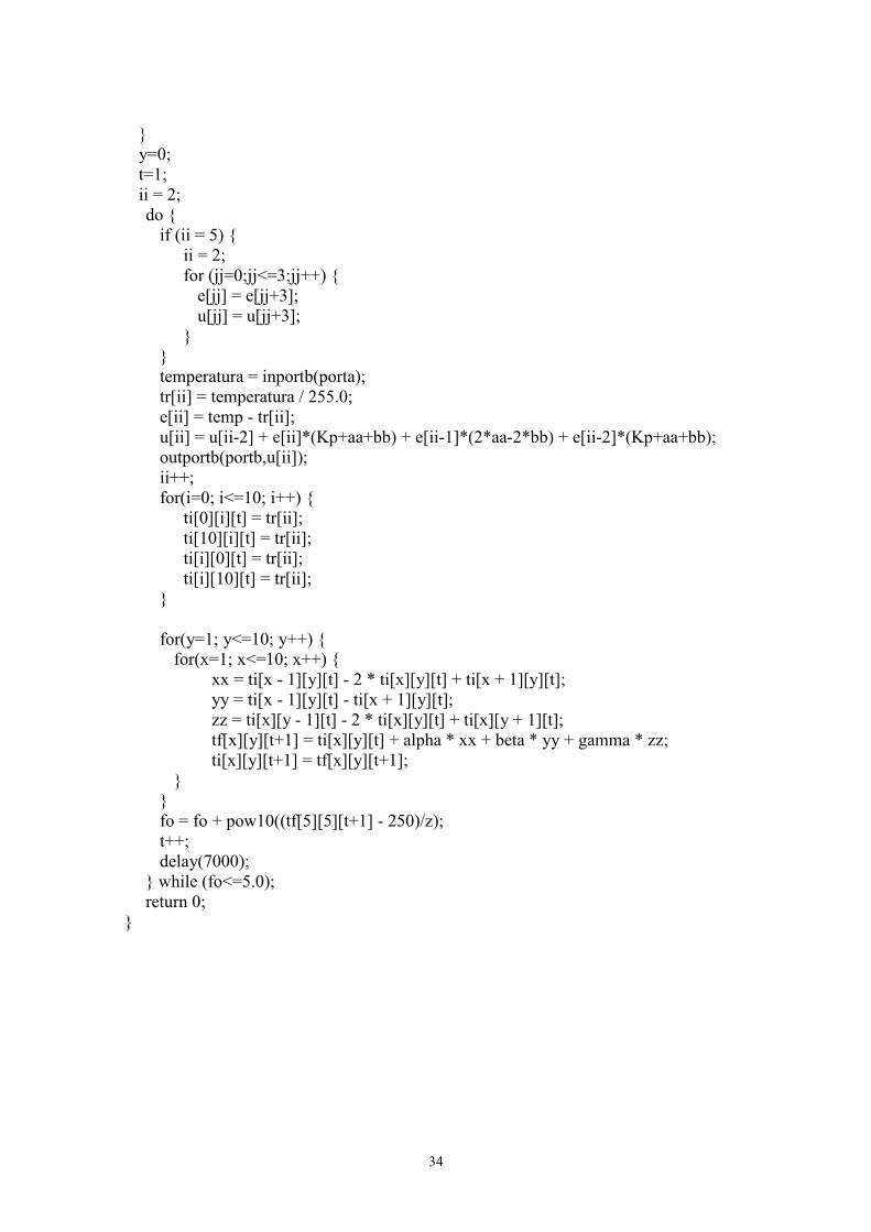
34
y=0;
t=1;
ii = 2;
do
if (ii = 5)
ii = 2;
for (jj=0;jj<=3;jj++)
e[jj] = e[jj+3];
u[jj] = u[jj+3];
temperatura = inportb(porta);
tr[ii] = temperatura / 255.0;
e[ii] = temp - tr[ii];
u[ii] = u[ii-2] + e[ii]*(Kp+aa+bb) + e[ii-1]*(2*aa-2*bb) + e[ii-2]*(Kp+aa+bb);
outportb(portb,u[ii]);
ii++;
for(i=0; i<=10; i++)
ti[0][i][t] = tr[ii];
ti[10][i][t] = tr[ii];
ti[i][0][t] = tr[ii];
ti[i][10][t] = tr[ii];
for(y=1; y<=10; y++)
for(x=1; x<=10; x++)
xx = ti[x - 1][y][t] - 2 * ti[x][y][t] + ti[x + 1][y][t];
yy = ti[x - 1][y][t] - ti[x + 1][y][t];
zz = ti[x][y - 1][t] - 2 * ti[x][y][t] + ti[x][y + 1][t];
tf[x][y][t+1] = ti[x][y][t] + alpha * xx + beta * yy + gamma * zz;
ti[x][y][t+1] = tf[x][y][t+1];
fo = fo + pow10((tf[5][5][t+1] - 250)/z);
t++;
delay(7000);
while (fo<=5.0);
return 0;

35
36
CAPITULO III
SIMULACIÓN
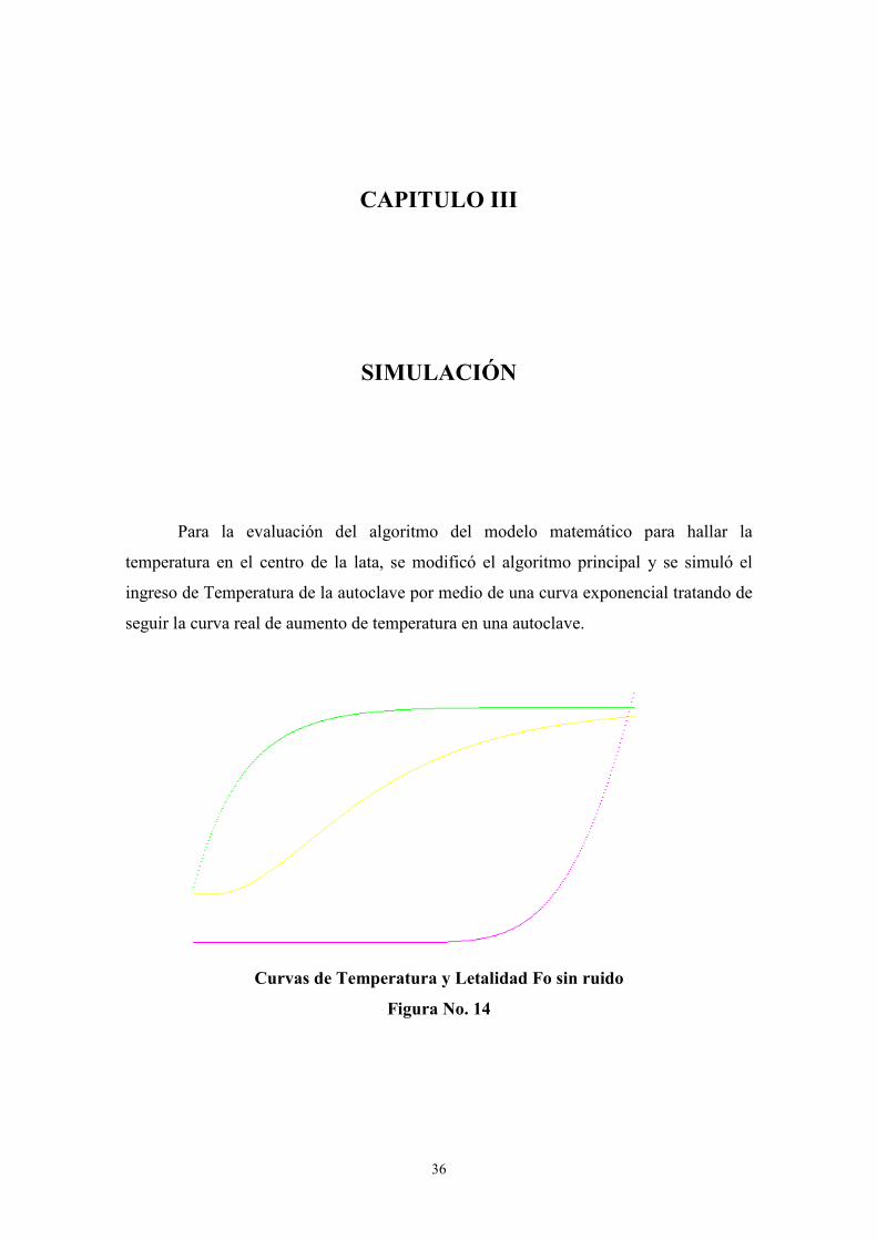
Para la evaluación del algoritmo del modelo matemático para hallar la
temperatura en el centro de la lata, se modificó el algoritmo principal y se simuló el
ingreso de Temperatura de la autoclave por medio de una curva exponencial tratando de
seguir la curva real de aumento de temperatura en una autoclave.
Curvas de Temperatura y Letalidad Fo sin ruido
Figura No. 14
37
En la figura 14, podemos observar que la Temperatura de la Autoclave (simulada)
es de color verde y es de forma exponencial con tendencia a llegar a 240 º F. La
temperatura en el centro de la lata es de color amarillo y es de forma exponencial con un
tiempo muerto y que trata de seguir a la temperatura de la autoclave. La curva de letalidad
Fo es de color magenta y es una curva exponencial bastante pronunciada.
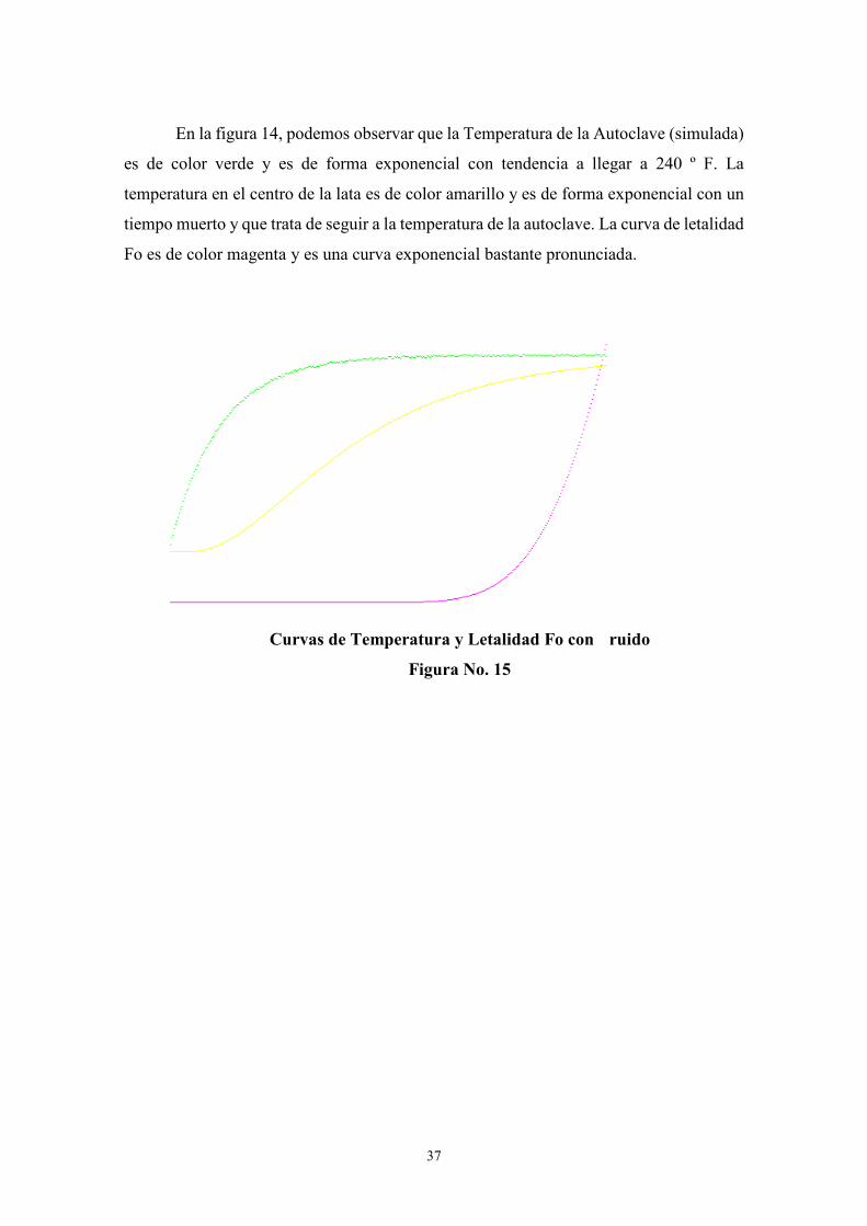
Curvas de Temperatura y Letalidad Fo con ruido
Figura No. 15
38
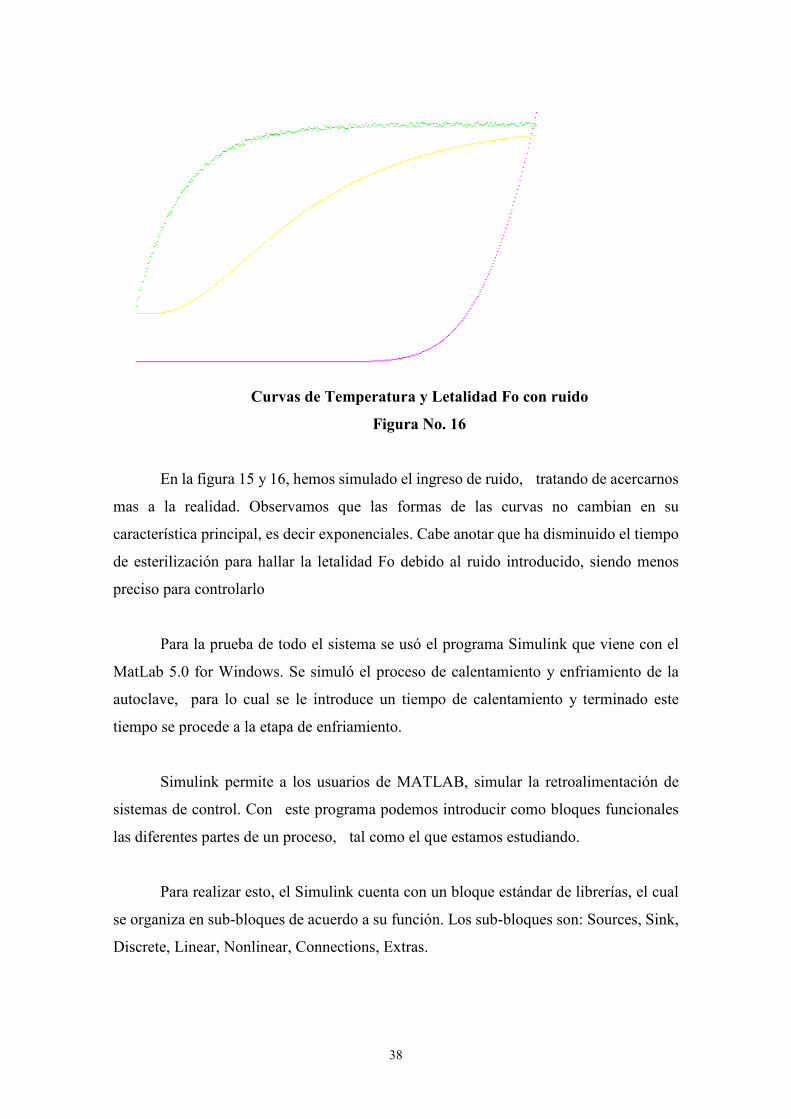
Curvas de Temperatura y Letalidad Fo con ruido
Figura No. 16
En la figura 15 y 16, hemos simulado el ingreso de ruido, tratando de acercarnos
mas a la realidad. Observamos que las formas de las curvas no cambian en su
característica principal, es decir exponenciales. Cabe anotar que ha disminuido el tiempo
de esterilización para hallar la letalidad Fo debido al ruido introducido, siendo menos
preciso para controlarlo
Para la prueba de todo el sistema se usó el programa Simulink que viene con el
MatLab 5.0 for Windows. Se simuló el proceso de calentamiento y enfriamiento de la
autoclave, para lo cual se le introduce un tiempo de calentamiento y terminado este
tiempo se procede a la etapa de enfriamiento.
Simulink permite a los usuarios de MATLAB, simular la retroalimentación de
sistemas de control. Con este programa podemos introducir como bloques funcionales
las diferentes partes de un proceso, tal como el que estamos estudiando.
Para realizar esto, el Simulink cuenta con un bloque estándar de librerías, el cual
se organiza en sub-bloques de acuerdo a su función. Los sub-bloques son: Sources, Sink,
Discrete, Linear, Nonlinear, Connections, Extras.
39
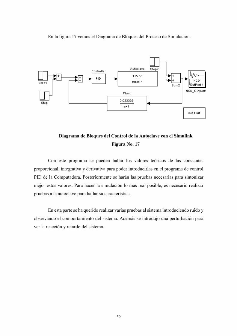
En la figura 17 vemos el Diagrama de Bloques del Proceso de Simulación.
Diagrama de Bloques del Control de la Autoclave con el Simulink
Figura No. 17
Con este programa se pueden hallar los valores teóricos de las constantes
proporcional, integrativa y derivativa para poder introducirlas en el programa de control
PID de la Computadora. Posteriormente se harán las pruebas necesarias para sintonizar
mejor estos valores. Para hacer la simulación lo mas real posible, es necesario realizar
pruebas a la autoclave para hallar su característica.
En esta parte se ha querido realizar varias pruebas al sistema introduciendo ruido y
observando el comportamiento del sistema. Además se introdujo una perturbación para
ver la reacción y retardo del sistema.
40
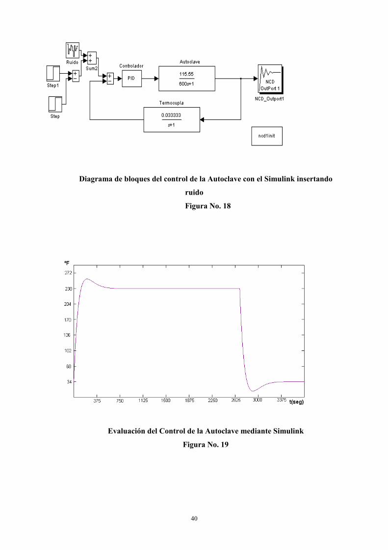
Diagrama de bloques del control de la Autoclave con el Simulink insertando
ruido
Figura No. 18
Evaluación del Control de la Autoclave mediante Simulink
Figura No. 19
41
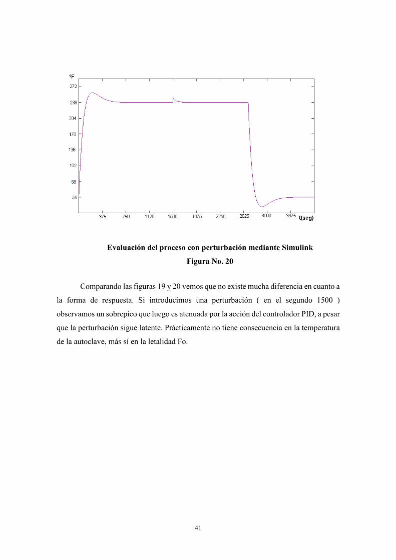
Evaluación del proceso con perturbación mediante Simulink
Figura No. 20
Comparando las figuras 19 y 20 vemos que no existe mucha diferencia en cuanto a
la forma de respuesta. Si introducimos una perturbación ( en el segundo 1500 )
observamos un sobrepico que luego es atenuada por la acción del controlador PID, a pesar
que la perturbación sigue latente. Prácticamente no tiene consecuencia en la temperatura
de la autoclave, más sí en la letalidad Fo.
42
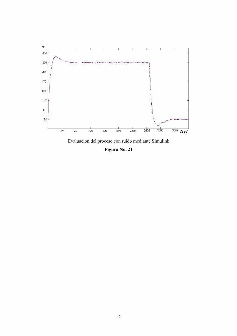
Evaluación del proceso con ruido mediante Simulink
Figura No. 21
43
CAPITULO IV
CONCLUSIONES Y RECOMENDACIONES
La presente investigación nos permite la evaluación de un modelo de
penetración de calor y también la simulación de su comportamiento gracias al algoritmo
de control desarrollado para este tipo de trabajo. Obteniendo la Letalidad Comercial o
de Diseño de conservas de pescado en forma automática .
En la implementación para este sistema podemos destacar el uso del controlador
PID por sus características más optimas para este tipo de trabajo ( control de temperatura
y procesos lentos ).
Gracias a un programa en Lenguaje C podemos observar la evaluación completa
del sistema de control automático para hallar la Letalidad Fo de conservas de pescado.
Se recomienda el uso del programa de simulación SIMULINK (herramienta de
simulación de procesos de control retroalimentados que viene con el MATHLAB ) para
obtener una mejor evaluación en estos tipos de sistemas de control por computadora.
44
Este diseño puede ser proyectado para el control de varias autoclaves mediante el
uso de varias tarjetas acondicionadoras de temperatura conectados a los sensores de
temperatura de las mismas. Así mismo es necesario el uso de multiplexores analógicos
para la conversión A/D. El programa tendría que modificarse para realizar una lectura
secuencial de todas las autoclaves y así calcular la Letalidad Fo de cada proceso.
En algunas plantas de conservas de pescado, la distancia entre las autoclaves y
Oficina de Control de Producción es grande, además muchas veces casi imposible
realizar un tendido de cables para llevar las señales de medición y control. En este tipo de
plantas se recomendaría el uso de enlaces radioeléctricos para una mejor implementación
y supervisión del proceso de Esterilización.
En la implementación de este diseño se han usado circuitos integrados que se
encuentran fácilmente en el mercado local. Por ejemplo el uso de un Conversor A/D de
resolución de 8 bits en vez de uno de 12 bits.
Se recomienda el uso del Lenguaje de programación Visual C o Visual Basic, ya
que con ellos es posible realizar una interface más sencilla entre el operador de la planta y
la computadora para la visualización de las medidas de temperaturas de las autoclaves y
de los valores de la Letalidad Fo, tanto en forma numérica como en forma gráfica.
45
ANEXO 1
TERMOCUPLAS
La termocupla es uno de los más simples y más comúnmente usados métodos para
determinar las temperaturas de los procesos. Cuando se requiere una indicación remota y
lecturas periódicas y cuando varios puntos deben ser mostrados en un sólo dispositivo de
lectura, ningún otro método de medición puede competir en costo-beneficio.
En 1821, T.J. Seebeck descubrió que cuando se aplicaba calor a una juntura de dos
metales distintos, se generaba una fuerza electromotriz (fem.), la cual podía medirse en la
otra juntura (fría) de estos dos metales (conductores). Estos contactores forman un
circuito eléctrico y la corriente fluye como resultado de la fem. generada, la corriente
seguirá fluyendo en tal circuito (figura 1) mientras T1=/=T2. El conductor B es descrito
como negativo con respecto al conductor A cuando la corriente fluye dentro de él en la
juntura fría. Este conductor negativo es siempre de color rojo (normas ISA y ANSI) como
una forma conveniente de determinar la polaridad correcta al conectar termocuplas.
46
Metal A(+)
Fem. = E
Metal B (-)
Temperatura Zona T1 T1 > T2 Temperatura Zona T2
Diagrama de una Termocupla
Figura No. 1
En la industria, las termocuplas se utilizan para medir temperatura en forma
exacta con propósitos de indicación, registro o control de procesos. Una juntura simple de
dos metales distintos (una termocupla) puede ser sometida a una temperatura a ser medida
y su fem. térmica puede ser comparada a una carta de referencia para obtener la
temperatura correspondiente. Desde que la temperatura de la segunda junta de los
metales debe ser conocida, se requiere mantenerla a un valor referencial (comúnmente
0°C). Existen diversas formas para mantener constante la temperatura de esta “unión
fría”, los cuales se pueden observar en la figura 2 ; se puede mantener a 0°C esa unión de
referencia, mediante un baño de hielo (a), lo cual no es práctico por razones obvias.
Compensación de una Termocupla
Figura No. 2
47
En cuanto a los materiales empleados para construir termocuplas o termopares, se
pueden observar algunas combinaciones de ellos, así como su rango de aplicación, salida
en mV/°Cs y los errores máximos en la medición en la tabla 1 la figura 3, da la respuesta
en función de la temperatura de algunos termopares.
Curva de diferentes tipos de Termocupla
Figura No. 3
48
Tabla de valores de diferentes tipos de Termocuplas
Tabla No.1
La selección del tipo de termocupla adecuado a un proceso en particular no
solamente depende del rango de medición sino de otras condiciones adicionales. Por
ejemplo, el termopar tipo J, es adecuado en atmósferas con escaso oxígeno libre, sin
embargo, la oxidación del hilo de hierro aumenta rápidamente por encima de 550°C
siendo necesario un mayor diámetro de hilo hasta una temperatura límite de 750°C. El
termopar tipo K, se recomienda en atmósferas oxidantes y a temperaturas de trabajo entre
500 y 1,000°C. No debe ser utilizado en atmósferas reductoras ni sulfurosas a menos que
esté protegido con un tubo de protección. Las termocuplas R y S se emplean en
atmósferas oxidantes y temperaturas de trabajo de hasta 1,500°C. Si la atmósfera no es
oxidante, el termopar debe protegerse con un tubo cerámico estanco; estas termocuplas se
49
emplean como cartuchos en la fabricación de acero en fusión. Se enchufan a una lanza y
el operario sumerge ésta en acero y aunque el cartucho se funde en pocos segundos, da
tiempo a que un circuito especial fije la máxima temperatura alcanzada. Finalmente el
termopar tipo T tiene una elevada resistencia a la corrosión por humedad atmosférica o
condensación y puede utilizarse en atmósferas oxidantes o reductoras.
En suma la selección de los alambres de termopares se hace en forma que tengan
una resistencia adecuada a la corrosión o la oxidación, a la reducción y a la cristalización;
que desarrolla una fem. relativamente alta, que sean estables, de bajo costo y de baja
resistencia eléctrica y que la relación entre la temperatura y la fem. sea tal que el aumento
de ésta sea (aproximadamente) paralelo al aumento de temperatura.
Con el advenimiento de instrumentos modernos de medición de gran impedancia
de entrada, se incrementa la posibilidad de que un sistema de medición de temperatura
con termocuplas se vea afectado por ruidos de diferentes tipos como estáticos,
magnéticos y de modo común. El primero es causado por el campo eléctrico proveniente
de una fuente de voltaje y que se acopla capacitivamente al circuito de la termocupla. Para
evitar esto se forran los cables con una malla metálica y se conecta esta a tierra. El ruido
magnético se produce por corrientes que fluyen por conductores eléctricos. Así, este
ruido se monta sobre una señal de medición y para evitarlo la mejor forma es “entorchar”
los cables de la termocupla. La interferencia de modo común se presenta cuando se tienen
dos tierras distintas en un circuito con la corriente circulando entre ellas. Esto es típico en
termocuplas con juntura a tierra (conectadas a su termopozo). Para evitar el problema
sólo se debe conectar la malla en un sólo punto, de lo contrario se producirá más ruido;
aparecerá en vez de ser eliminado.
50
COMPUTADOR
SEÑALES DE CONTROL AL ELEMENTO FINAL DE CONTROL(VALVULA DE CONTROL DE VAPOR )
TEMPERATURA DE LA TERMOCUPLA TIPO T
FUNCIONES DEL COMPUTADOR :- A C O N D I O N A M I E N T O D E L ATEMPERATURA.- CONVERSION ANALOGO-DIGITAL- C O N T R O L D E V A L V U L A D EAUTOCLVE-ALGORTMO DE CONTROL PID-ALGORITMO PARA HALLA LETALIDAD
T
AUTOCLAVE
CARRO TRANSPORTADOR DE LATAS DECONSERVA DE PESCADO
TERMOCUPLA


IMPORTANT NOTICE
Texas Instruments and its subsidiaries (TI) reserve the right to make changes to their products or to discontinueany product or service without notice, and advise customers to obtain the latest version of relevant informationto verify, before placing orders, that information being relied on is current and complete. All products are soldsubject to the terms and conditions of sale supplied at the time of order acknowledgement, including thosepertaining to warranty, patent infringement, and limitation of liability.
TI warrants performance of its semiconductor products to the specifications applicable at the time of sale inaccordance with TI’s standard warranty. Testing and other quality control techniques are utilized to the extentTI deems necessary to support this warranty. Specific testing of all parameters of each device is not necessarilyperformed, except those mandated by government requirements.
CERTAIN APPLICATIONS USING SEMICONDUCTOR PRODUCTS MAY INVOLVE POTENTIAL RISKS OFDEATH, PERSONAL INJURY, OR SEVERE PROPERTY OR ENVIRONMENTAL DAMAGE (“CRITICALAPPLICATIONS”). TI SEMICONDUCTOR PRODUCTS ARE NOT DESIGNED, AUTHORIZED, ORWARRANTED TO BE SUITABLE FOR USE IN LIFE-SUPPORT DEVICES OR SYSTEMS OR OTHERCRITICAL APPLICATIONS. INCLUSION OF TI PRODUCTS IN SUCH APPLICATIONS IS UNDERSTOOD TOBE FULLY AT THE CUSTOMER’S RISK.
In order to minimize risks associated with the customer’s applications, adequate design and operatingsafeguards must be provided by the customer to minimize inherent or procedural hazards.
TI assumes no liability for applications assistance or customer product design. TI does not warrant or representthat any license, either express or implied, is granted under any patent right, copyright, mask work right, or otherintellectual property right of TI covering or relating to any combination, machine, or process in which suchsemiconductor products or services might be or are used. TI’s publication of information regarding any thirdparty’s products or services does not constitute TI’s approval, warranty or endorsement thereof.
Copyright 1998, Texas Instruments Incorporated
6-5
Features• 80C48 and 80C80/85 Bus Compatible - No Interfacing
Logic Required
• Conversion Time < 100 µs
• Easy Interface to Most Microprocessors
• Will Operate in a “Stand Alone” Mode
• Differential Analog Voltage Inputs
• Works with Bandgap Voltage References
• TTL Compatible Inputs and Outputs
• On-Chip Clock Generator
• 0V to 5V Analog Voltage Input Range (Single + 5V Supply)
• No Zero-Adjust Required
DescriptionThe ADC0802 family are CMOS 8-Bit, successive-approxi-mation A/D converters which use a modified potentiometricladder and are designed to operate with the 8080A controlbus via three-state outputs. These converters appear to theprocessor as memory locations or I/O ports, and hence nointerfacing logic is required.
The differential analog voltage input has good common-mode-rejection and permits offsetting the analog zero-input-voltage value. In addition, the voltage reference input can beadjusted to allow encoding any smaller analog voltage spanto the full 8 bits of resolution.
Ordering Information
PART NUMBER ERROR EXTERNAL CONDITIONS TEMP. RANGE ( oC) PACKAGE PKG. NO
ADC0802LCN ±1/2 LSB VREF/2 = 2.500VDC (No Adjustments) 0 to 70 20 Ld PDIP E20.3
ADC0802LCD ±3/4 LSB -40 to 85 20 Ld CERDIP F20.3
ADC0802LD ±1 LSB -55 to 125 20 Ld CERDIP F20.3
ADC0803LCN ±1/2 LSB VREF/2 Adjusted for Correct Full ScaleReading
0 to 70 20 Ld PDIP E20.3
ADC0803LCD ±3/4 LSB -40 to 85 20 Ld CERDIP F20.3
ADC0803LCWM ±1 LSB -40 to 85 20 Ld SOIC M20.3
ADC0803LD ±1 LSB -55 to 125 20 Ld CERDIP F20.3
ADC0804LCN ±1 LSB VREF/2 = 2.500VDC (No Adjustments) 0 to 70 20 Ld PDIP E20.3
ADC0804LCD ±1 LSB -40 to 85 20 Ld CERDIP F20.3
ADC0804LCWM ±1 LSB -40 to 85 20 Ld SOIC M20.3
PinoutADC0802, ADC0803, ADC0804
(PDIP, CERDIP)TOP VIEW
Typical Application Schematic
11
12
13
14
15
16
17
18
20
19
10
9
8
7
6
5
4
3
2
1
WR
RD
CS
CLK IN
INTR
VIN (-)
VIN (+)
DGND
VREF/2
AGND
V+ OR VREF
CLK R
DB0 (LSB)
DB1
DB2
DB3
DB4
DB5
DB6
DB7 (MSB)
3
2
1
12
11
5
15
14
13
18
17
16
7
6
10
9
8
4
19
20
WR
RD
CS
DB6
DB7
INTR
DB3
DB4
DB5
DB0
DB1
DB2
CLK IN
CLK R
V+
VIN (-)
VIN (+)
DGND
VREF/2
AGND
ANYµPROCESSOR 8-BIT RESOLUTION
OVER ANYDESIREDANALOG INPUTVOLTAGE RANGE
DIFFINPUTS
10K
150pF
VREF/2
µP B
US
+5V
August 1997
ADC0802, ADC0803ADC0804
8-Bit, Microprocessor-Compatible, A/D Converters
File Number 3094.1CAUTION: These devices are sensitive to electrostatic discharge; follow proper IC Handling Procedures.http://www.intersil.com or 407-727-9207 | Copyright © Intersil Corporation 1999
6-6
Functional Diagram
1211 151413 181716
WR
RD
CS
INTR
CLK OSC
CLK R
V+
VIN (-)
VIN (+)
DGND
VREF/2
AGND
(VREF)
DACVOUT
COMP
CLK GEN CLKS
CLK ARESET
START F/F
LADDERAND
DECODER
SUCCESSIVEAPPROX.
REGISTERAND LATCH
8-BITSHIFT
REGISTER
D
RESET
SET
CONV. COMPL.
THREE-STATEOUTPUT LATCHES
DIGITAL OUTPUTS
THREE-STATE CONTROL“1” = OUTPUT ENABLE
DFF2
CLK A
XFERG2
Q
8 X 1/f
R
Q
INTR F/F
IF RESET = “0”
D
DFF1Q
D
Q
CLK B STARTCONVERSION
MSB
LSB
Q“1” = RESET SHIFT REGISTER“0” = BUSY AND RESET STATE RESET
READ
SET3
2
1
5
7
6
10
9
8
4
19
20
CLK IN
MSB
G1
CLK
-+
LSB
INPUT PROTECTIONFOR ALL LOGIC INPUTS
INPUTTO INTERNAL
BV = 30V
CIRCUITS
∑
V+
+
-
ADC0802, ADC0803, ADC0804
6-7
Absolute Maximum Ratings Thermal InformationSupply Voltage . . . . . . . . . . . . . . . . . . . . . . . . . . . . . . . . . . . . . . 6.5VVoltage at Any Input . . . . . . . . . . . . . . . . . . . . . . -0.3V to (V+ +0.3V)
Operating ConditionsTemperature Range
ADC0802/03LD. . . . . . . . . . . . . . . . . . . . . . . . . . . -55oC to 125oCADC0802/03/04LCD . . . . . . . . . . . . . . . . . . . . . . . . -40oC to 85oCADC0802/03/04LCN . . . . . . . . . . . . . . . . . . . . . . . . . .0oC to 70oCADC0803/04LCWM . . . . . . . . . . . . . . . . . . . . . . . . -40oC to 85oC
Thermal Resistance (Typical, Note 1) θJA (oC/W) θJC (oC/W)PDIP Package . . . . . . . . . . . . . . . . . . . . . 125 N/ACERDIP Package . . . . . . . . . . . . . . . . . . 80 20SOIC Package . . . . . . . . . . . . . . . . . . . . . 120 N/A
Maximum Junction TemperatureHermetic Package . . . . . . . . . . . . . . . . . . . . . . . . . . . . . . . . 175oCPlastic Package . . . . . . . . . . . . . . . . . . . . . . . . . . . . . . . . . . 150oC
Maximum Storage Temperature Range . . . . . . . . . .-65oC to 150oCMaximum Lead Temperature (Soldering, 10s) . . . . . . . . . . . . 300oC
(SOIC - Lead Tips Only)
CAUTION: Stresses above those listed in “Absolute Maximum Ratings” may cause permanent damage to the device. This is a stress only rating and operationof the device at these or any other conditions above those indicated in the operational sections of this specification is not implied.
NOTE:
1. θJA is measured with the component mounted on an evaluation PC board in free air.
Electrical Specifications (Notes 1, 7)
PARAMETER TEST CONDITIONS MIN TYP MAX UNITS
CONVERTER SPECIFICATIONS V+ = 5V, TA = 25oC and fCLK = 640kHz, Unless Otherwise Specified
Total Unadjusted Error
ADC0802 VREF/2 = 2.500V - - ±1/2 LSB
ADC0803 VREF/2 Adjusted for Correct FullScale Reading
- - ±1/2 LSB
ADC0804 VREF/2 = 2.500V - - ±1 LSB
VREF/2 Input Resistance Input Resistance at Pin 9 1.0 1.3 - kΩ
Analog Input Voltage Range (Note 2) GND-0.05 - (V+) + 0.05 V
DC Common-Mode Rejection Over Analog Input Voltage Range - ±1/16 ±1/8 LSB
Power Supply Sensitivity V+ = 5V ±10% Over Allowed InputVoltage Range
- ±1/16 ±1/8 LSB
CONVERTER SPECIFICATIONS V+ = 5V, 0oC to 70oC and fCLK = 640kHz, Unless Otherwise Specified
Total Unadjusted Error
ADC0802 VREF/2 = 2.500V - - ±1/2 LSB
ADC0803 VREF/2 Adjusted for Correct FullScale Reading
- - ±1/2 LSB
ADC0804 VREF/2 = 2.500V - - ±1 LSB
VREF/2 Input Resistance Input Resistance at Pin 9 1.0 1.3 - kΩ
Analog Input Voltage Range (Note 2) GND-0.05 - (V+) + 0.05 V
DC Common-Mode Rejection Over Analog Input Voltage Range - ±1/8 ±1/4 LSB
Power Supply Sensitivity V+ = 5V ±10% Over Allowed InputVoltage Range
- ±1/16 ±1/8 LSB
CONVERTER SPECIFICATIONS V+ = 5V, -25oC to 85oC and fCLK = 640kHz, Unless Otherwise Specified
Total Unadjusted Error
ADC0802 VREF/2 = 2.500V - - ±3/4 LSB
ADC0803 VREF/2 Adjusted for Correct FullScale Reading
- - ±3/4 LSB
ADC0804 VREF/2 = 2.500V - - ±1 LSB
VREF/2 Input Resistance Input Resistance at Pin 9 1.0 1.3 - kΩ
Analog Input Voltage Range (Note 2) GND-0.05 - (V+) + 0.05 V
DC Common-Mode Rejection Over Analog Input Voltage Range - ±1/8 ±1/4 LSB
Power Supply Sensitivity V+ = 5V ±10% Over Allowed InputVoltage Range
- ±1/16 ±1/8 LSB
ADC0802, ADC0803, ADC0804
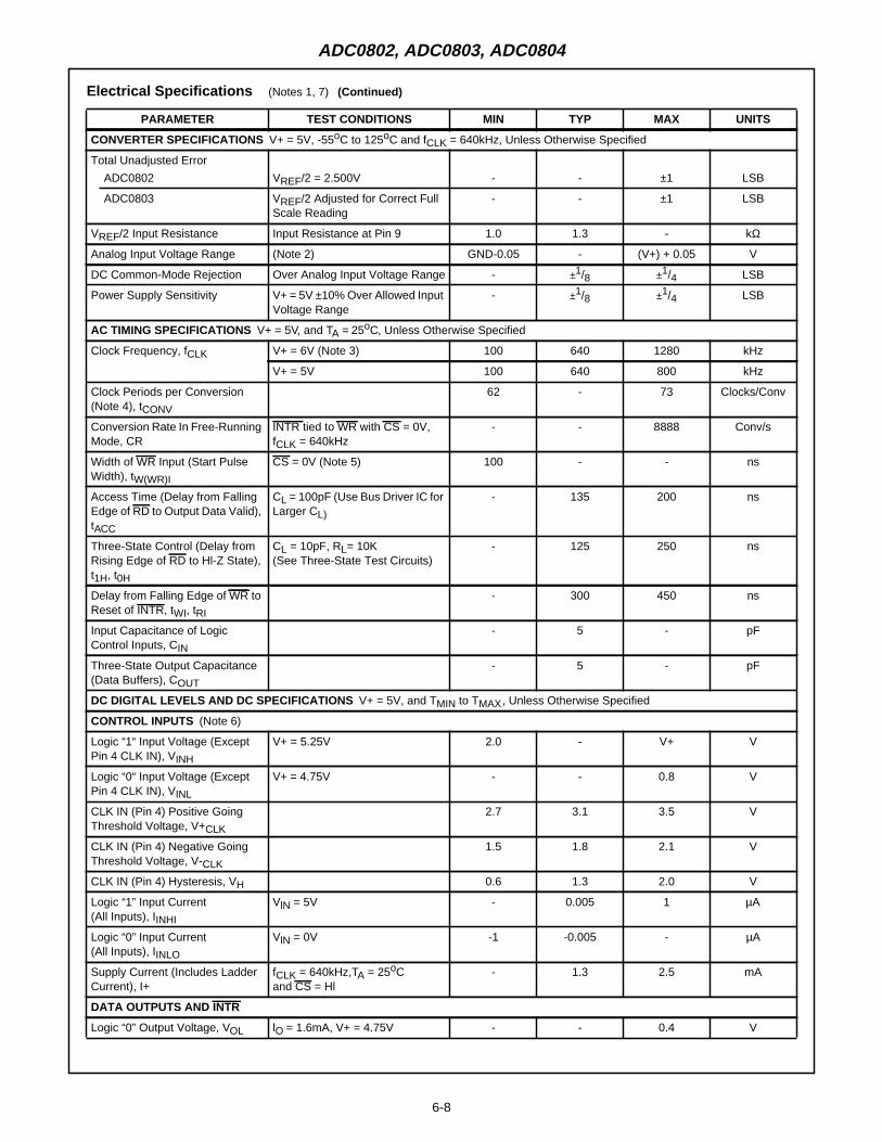
6-8
CONVERTER SPECIFICATIONS V+ = 5V, -55oC to 125oC and fCLK = 640kHz, Unless Otherwise Specified
Total Unadjusted Error
ADC0802 VREF/2 = 2.500V - - ±1 LSB
ADC0803 VREF/2 Adjusted for Correct FullScale Reading
- - ±1 LSB
VREF/2 Input Resistance Input Resistance at Pin 9 1.0 1.3 - kΩ
Analog Input Voltage Range (Note 2) GND-0.05 - (V+) + 0.05 V
DC Common-Mode Rejection Over Analog Input Voltage Range - ±1/8 ±1/4 LSB
Power Supply Sensitivity V+ = 5V ±10% Over Allowed InputVoltage Range
- ±1/8 ±1/4 LSB
AC TIMING SPECIFICATIONS V+ = 5V, and TA = 25oC, Unless Otherwise Specified
Clock Frequency, fCLK V+ = 6V (Note 3) 100 640 1280 kHz
V+ = 5V 100 640 800 kHz
Clock Periods per Conversion(Note 4), tCONV
62 - 73 Clocks/Conv
Conversion Rate In Free-RunningMode, CR
INTR tied to WR with CS = 0V,fCLK = 640kHz
- - 8888 Conv/s
Width of WR Input (Start PulseWidth), tW(WR)I
CS = 0V (Note 5) 100 - - ns
Access Time (Delay from FallingEdge of RD to Output Data Valid),tACC
CL = 100pF (Use Bus Driver IC forLarger CL)
- 135 200 ns
Three-State Control (Delay fromRising Edge of RD to Hl-Z State),t1H, t0H
CL = 10pF, RL= 10K(See Three-State Test Circuits)
- 125 250 ns
Delay from Falling Edge of WR toReset of INTR, tWI, tRI
- 300 450 ns
Input Capacitance of LogicControl Inputs, CIN
- 5 - pF
Three-State Output Capacitance(Data Buffers), COUT
- 5 - pF
DC DIGITAL LEVELS AND DC SPECIFICATIONS V+ = 5V, and TMIN to TMAX, Unless Otherwise Specified
CONTROL INPUTS (Note 6)
Logic “1“ Input Voltage (ExceptPin 4 CLK IN), VINH
V+ = 5.25V 2.0 - V+ V
Logic “0“ Input Voltage (ExceptPin 4 CLK IN), VINL
V+ = 4.75V - - 0.8 V
CLK IN (Pin 4) Positive GoingThreshold Voltage, V+CLK
2.7 3.1 3.5 V
CLK IN (Pin 4) Negative GoingThreshold Voltage, V-CLK
1.5 1.8 2.1 V
CLK IN (Pin 4) Hysteresis, VH 0.6 1.3 2.0 V
Logic “1” Input Current(All Inputs), IINHI
VlN = 5V - 0.005 1 µΑ
Logic “0” Input Current(All Inputs), IINLO
VlN = 0V -1 -0.005 - µA
Supply Current (Includes LadderCurrent), I+
fCLK = 640kHz,TA = 25oCand CS = Hl
- 1.3 2.5 mA
DATA OUTPUTS AND INTR
Logic “0” Output Voltage, VOL lO = 1.6mA, V+ = 4.75V - - 0.4 V
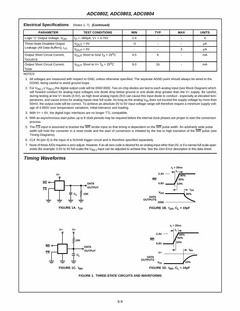
Electrical Specifications (Notes 1, 7) (Continued)
PARAMETER TEST CONDITIONS MIN TYP MAX UNITS
ADC0802, ADC0803, ADC0804
6-9
Logic “1” Output Voltage, VOH lO = -360µA, V+ = 4.75V 2.4 - - V
Three-State Disabled OutputLeakage (All Data Buffers), ILO
VOUT = 0V -3 - - µA
VOUT = 5V - - 3 µA
Output Short Circuit Current,ISOURCE
VOUT Short to Gnd TA = 25oC 4.5 6 - mA
Output Short Circuit Current,ISINK
VOUT Short to V+ TA = 25oC 9.0 16 - mA
NOTES:
1. All voltages are measured with respect to GND, unless otherwise specified. The separate AGND point should always be wired to theDGND, being careful to avoid ground loops.
2. For VIN(-) ≥ VIN(+) the digital output code will be 0000 0000. Two on-chip diodes are tied to each analog input (see Block Diagram) whichwill forward conduct for analog input voltages one diode drop below ground or one diode drop greater than the V+ supply. Be careful,during testing at low V+ levels (4.5V), as high level analog inputs (5V) can cause this input diode to conduct - especially at elevated tem-peratures, and cause errors for analog inputs near full scale. As long as the analog VIN does not exceed the supply voltage by more than50mV, the output code will be correct. To achieve an absolute 0V to 5V input voltage range will therefore require a minimum supply volt-age of 4.950V over temperature variations, initial tolerance and loading.
3. With V+ = 6V, the digital logic interfaces are no longer TTL compatible.
4. With an asynchronous start pulse, up to 8 clock periods may be required before the internal clock phases are proper to start the conversionprocess.
5. The CS input is assumed to bracket the WR strobe input so that timing is dependent on the WR pulse width. An arbitrarily wide pulsewidth will hold the converter in a reset mode and the start of conversion is initiated by the low to high transition of the WR pulse (seeTiming Diagrams).
6. CLK IN (pin 4) is the input of a Schmitt trigger circuit and is therefore specified separately.
7. None of these A/Ds requires a zero-adjust. However, if an all zero code is desired for an analog input other than 0V, or if a narrow full scale spanexists (for example: 0.5V to 4V full scale) the VIN(-) input can be adjusted to achieve this. See the Zero Error description in this data sheet.
Electrical Specifications (Notes 1, 7) (Continued)
PARAMETER TEST CONDITIONS MIN TYP MAX UNITS
Timing Waveforms
FIGURE 1A. t1H FIGURE 1B. t1H, CL = 10pF
FIGURE 1C. t0H FIGURE 1D. t0H, CL = 10pF
FIGURE 1. THREE-STATE CIRCUITS AND WAVEFORMS
10K
V+
RD
CS
CL
DATAOUTPUT
RD
2.4Vtr
90%50%
10%
t1H
0.8V
DATAOUTPUTS
GND
tr = 20ns
VOH 90%
10K
V+
RD
CSCL
DATAOUTPUT
V+
RD
2.4V
tr
90%50%
10%
t0H
0.8V
DATAOUTPUTS
VOI
tr = 20ns
V+
10%
ADC0802, ADC0803, ADC0804
6-10
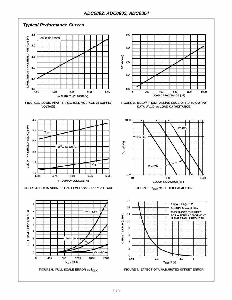
Typical Performance Curves
FIGURE 2. LOGIC INPUT THRESHOLD VOLTAGE vs SUPPLYVOLTAGE
FIGURE 3. DELAY FROM FALLING EDGE OF RD TO OUTPUTDATA VALID vs LOAD CAPACITANCE
FIGURE 4. CLK IN SCHMITT TRIP LEVELS vs SUPPLY VOLTAGE FIGURE 5. fCLK vs CLOCK CAPACITOR
FIGURE 6. FULL SCALE ERROR vs f CLK FIGURE 7. EFFECT OF UNADJUSTED OFFSET ERROR
-55oC TO 125oC1.8
1.7
1.6
1.5
1.4
1.34.754.50 5.00 5.25 5.50
V+ SUPPLY VOLTAGE (V)
LOG
IC IN
PU
T T
HR
ES
HO
LD V
OLT
AG
E (
V)
DE
LAY
(ns
)
500
400
300
200
1000
LOAD CAPACITANCE (pF)200 400 600 800 1000
CLK
IN T
HR
ES
HO
LD V
OLT
AG
E (
V)
3.5
3.1
2.7
2.3
1.9
1.54.50
V+ SUPPLY VOLTAGE (V)
-55oC TO 125oC
VT(-)
VT(+)
4.75 5.00 5.25 5.50
1000
CLOCK CAPACITOR (pF)
f CLK
(kH
z)
10010010 1000
R = 10K
R = 50K
R = 20K
FU
LL S
CA
LE E
RR
OR
(LS
Bs)
7
6
5
4
3
2
1
0
fCLK (kHz)0 400 800 1200 1600 2000
V+ = 4.5V
V+ = 5V
V+ = 6V
VIN(+) = VIN(-) = 0V
ASSUMES VOS = 2mV
THIS SHOWS THE NEEDFOR A ZERO ADJUSTMENTIF THE SPAN IS REDUCED
OF
FS
ET
ER
RO
R (
LSB
s)
16
14
12
10
8
6
4
2
VREF/2 (V)
00.01 0.1 1.0 5
ADC0802, ADC0803, ADC0804
6-11
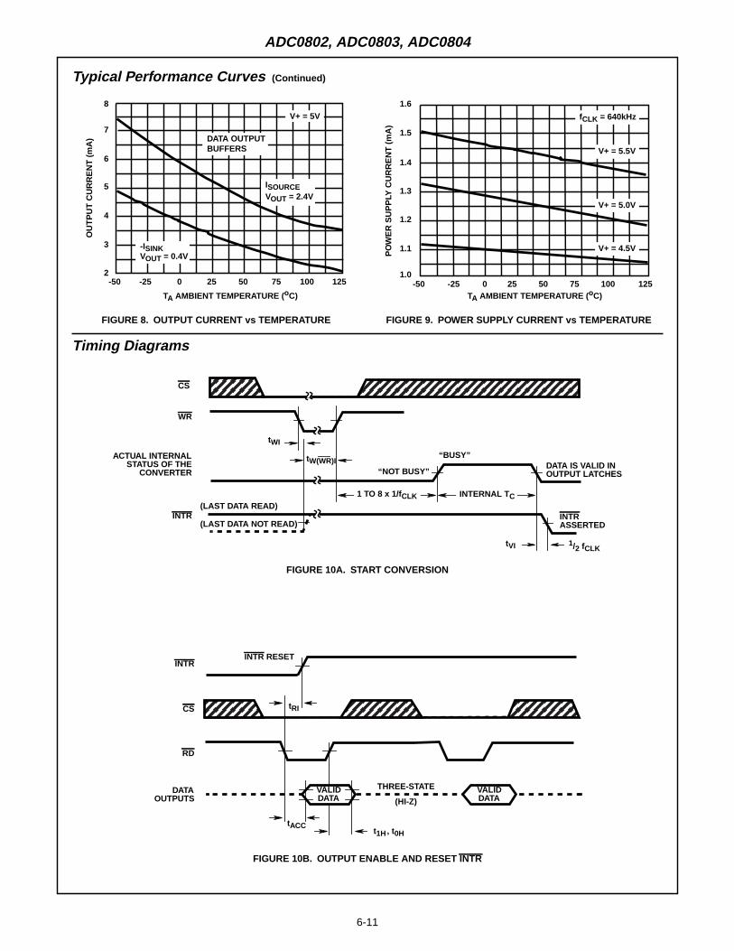
FIGURE 8. OUTPUT CURRENT vs TEMPERATURE FIGURE 9. POWER SUPPLY CURRENT vs TEMPERATURE
Timing Diagrams
FIGURE 10A. START CONVERSION
FIGURE 10B. OUTPUT ENABLE AND RESET INTR
Typical Performance Curves (Continued)O
UT
PU
T C
UR
RE
NT
(m
A)
8
7
6
5
4
3
2-50
TA AMBIENT TEMPERATURE ( oC)
-ISINKVOUT = 0.4V
ISOURCEVOUT = 2.4V
DATA OUTPUTBUFFERS
V+ = 5V
-25 0 25 50 75 100 125
PO
WE
R S
UP
PLY
CU
RR
EN
T (
mA
)
TA AMBIENT TEMPERATURE ( oC)-50 -25 0 25 50 75 100 125
1.6
1.5
1.4
1.3
1.2
1.1
1.0
fCLK = 640kHz
V+ = 5.5V
V+ = 5.0V
V+ = 4.5V
tWI
tW(WR)I
1 TO 8 x 1/fCLK INTERNAL TC
CS
WR
ACTUAL INTERNALSTATUS OF THE
CONVERTER
INTR(LAST DATA READ)
(LAST DATA NOT READ)
“NOT BUSY”
“BUSY”DATA IS VALID INOUTPUT LATCHES
INTRASSERTED
tVI 1/2 fCLK
VALIDDATA
VALIDDATA
INTR RESETINTR
CS
RD
DATAOUTPUTS
THREE-STATE
(HI-Z)
tRI
tACCt1H, t0H
ADC0802, ADC0803, ADC0804
6-12
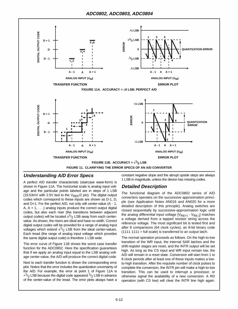
Understanding A/D Error SpecsA perfect A/D transfer characteristic (staircase wave-form) isshown in Figure 11A. The horizontal scale is analog input volt-age and the particular points labeled are in steps of 1 LSB(19.53mV with 2.5V tied to the VREF/2 pin). The digital outputcodes which correspond to these inputs are shown as D-1, D,and D+1. For the perfect A/D, not only will center-value (A - 1,A, A + 1, . . .) analog inputs produce the correct output digitalcodes, but also each riser (the transitions between adjacentoutput codes) will be located ±1/2 LSB away from each center-value. As shown, the risers are ideal and have no width. Correctdigital output codes will be provided for a range of analog inputvoltages which extend ±1/2 LSB from the ideal center-values.Each tread (the range of analog input voltage which providesthe same digital output code) is therefore 1 LSB wide.
The error curve of Figure 11B shows the worst case transferfunction for the ADC0802. Here the specification guaranteesthat if we apply an analog input equal to the LSB analog volt-age center-value, the A/D will produce the correct digital code.
Next to each transfer function is shown the corresponding errorplot. Notice that the error includes the quantization uncertainty ofthe A/D. For example, the error at point 1 of Figure 11A is+1/2 LSB because the digital code appeared 1/2 LSB in advanceof the center-value of the tread. The error plots always have a
constant negative slope and the abrupt upside steps are always1 LSB in magnitude, unless the device has missing codes.
Detailed DescriptionThe functional diagram of the ADC0802 series of A/Dconverters operates on the successive approximation princi-ple (see Application Notes AN016 and AN020 for a moredetailed description of this principle). Analog switches areclosed sequentially by successive-approximation logic untilthe analog differential input voltage [VlN(+) - VlN(-)] matchesa voltage derived from a tapped resistor string across thereference voltage. The most significant bit is tested first andafter 8 comparisons (64 clock cycles), an 8-bit binary code(1111 1111 = full scale) is transferred to an output latch.
The normal operation proceeds as follows. On the high-to-lowtransition of the WR input, the internal SAR latches and theshift-register stages are reset, and the INTR output will be sethigh. As long as the CS input and WR input remain low, theA/D will remain in a reset state. Conversion will start from 1 to8 clock periods after at least one of these inputs makes a low-to-high transition. After the requisite number of clock pulses tocomplete the conversion, the INTR pin will make a high-to-lowtransition. This can be used to interrupt a processor, orotherwise signal the availability of a new conversion. A RDoperation (with CS low) will clear the INTR line high again.
TRANSFER FUNCTION ERROR PLOT
FIGURE 11A. ACCURACY = ±0 LSB; PERFECT A/D
TRANSFER FUNCTION ERROR PLOT
FIGURE 11B. ACCURACY = ±1/2 LSB
FIGURE 11. CLARIFYING THE ERROR SPECS OF AN A/D CONVERTER
ANALOG INPUT (V IN)
DIG
ITA
L O
UT
PU
T C
OD
ED + 1
D
D - 1
A + 1AA - 1
3
21
5 6
4
3
2
1 5
64
ER
RO
R
0
+1 LSB
-1 LSB
-1/2 LSB
+1/2 LSB
* QUANTIZATION ERROR
A
ANALOG INPUT (V IN)
A + 1A - 1
ANALOG INPUT (V IN)
DIG
ITA
L O
UT
PU
T C
OD
E
D + 1
D
D - 1
A + 1AA - 1
3
21
5
6
4*0
+1 LSB
-1 LSB
QUANTIZATION
ER
RO
R
3
2
1
6
4
ANALOG INPUT (V IN)
A + 1AA - 1
ERROR
ADC0802, ADC0803, ADC0804
6-13
The device may be operated in the free-running mode by con-necting INTR to the WR input with CS = 0. To ensure start-upunder all possible conditions, an external WR pulse isrequired during the first power-up cycle. A conversion-in-pro-cess can be interrupted by issuing a second start command.
Digital Operation
The converter is started by having CS and WR simultaneouslylow. This sets the start flip-flop (F/F) and the resulting “1” levelresets the 8-bit shift register, resets the Interrupt (INTR) F/Fand inputs a “1” to the D flip-flop, DFF1, which is at the inputend of the 8-bit shift register. Internal clock signals then trans-fer this “1” to the Q output of DFF1. The AND gate, G1, com-bines this “1” output with a clock signal to provide a resetsignal to the start F/F. If the set signal is no longer present(either WR or CS is a “1”), the start F/F is reset and the 8-bitshift register then can have the “1” clocked in, which starts theconversion process. If the set signal were to still be present,this reset pulse would have no effect (both outputs of the startF/F would be at a “1” level) and the 8-bit shift register wouldcontinue to be held in the reset mode. This allows for asyn-chronous or wide CS and WR signals.
After the “1” is clocked through the 8-bit shift register (whichcompletes the SAR operation) it appears as the input toDFF2. As soon as this “1” is output from the shift register, theAND gate, G2, causes the new digital word to transfer to theThree-State output latches. When DFF2 is subsequentlyclocked, the Q output makes a high-to-low transition whichcauses the INTR F/F to set. An inverting buffer then suppliesthe INTR output signal.
When data is to be read, the combination of both CS and RDbeing low will cause the INTR F/F to be reset and the three-state output latches will be enabled to provide the 8-bit digitaloutputs.
Digital Control Inputs
The digital control inputs (CS, RD, and WR) meet standardTTL logic voltage levels. These signals are essentially equiva-lent to the standard A/D Start and Output Enable control sig-nals, and are active low to allow an easy interface tomicroprocessor control busses. For non-microprocessorbased applications, the CS input (pin 1) can be grounded andthe standard A/D Start function obtained by an active lowpulse at the WR input (pin 3). The Output Enable function isachieved by an active low pulse at the RD input (pin 2).
Analog Operation
The analog comparisons are performed by a capacitivecharge summing circuit. Three capacitors (with preciseratioed values) share a common node with the input to anauto-zeroed comparator. The input capacitor is switchedbetween VlN(+) and VlN(-), while two ratioed reference capaci-tors are switched between taps on the reference voltagedivider string. The net charge corresponds to the weighted dif-ference between the input and the current total value set bythe successive approximation register. A correction is made tooffset the comparison by 1/2 LSB (see Figure 11A).
Analog Differential Voltage Inputs and Common-ModeRejection
This A/D gains considerable applications flexibility from the ana-log differential voltage input. The VlN(-) input (pin 7) can be used
to automatically subtract a fixed voltage value from the inputreading (tare correction). This is also useful in 4mA - 20mA cur-rent loop conversion. In addition, common-mode noise can bereduced by use of the differential input.
The time interval between sampling VIN(+) and VlN(-) is 41/2clock periods. The maximum error voltage due to this slighttime difference between the input voltage samples is given by:
where:
∆VE is the error voltage due to sampling delay,
VPEAK is the peak value of the common-mode voltage,
fCM is the common-mode frequency.
For example, with a 60Hz common-mode frequency, fCM,and a 640kHz A/D clock, fCLK, keeping this error to 1/4 LSB(~5mV) would allow a common-mode voltage, VPEAK, givenby:
,
or
.
The allowed range of analog input voltage usually placesmore severe restrictions on input common-mode voltagelevels than this.
An analog input voltage with a reduced span and a relativelylarge zero offset can be easily handled by making use of thedifferential input (see Reference Voltage Span Adjust).
Analog Input Current
The internal switching action causes displacement currents toflow at the analog inputs. The voltage on the on-chip capaci-tance to ground is switched through the analog differentialinput voltage, resulting in proportional currents entering theVIN(+) input and leaving the VIN(-) input. These current tran-sients occur at the leading edge of the internal clocks. Theyrapidly decay and do not inherently cause errors as the on-chip comparator is strobed at the end of the clock perIod.
Input Bypass Capacitors
Bypass capacitors at the inputs will average these chargesand cause a DC current to flow through the output resistancesof the analog signal sources. This charge pumping action isworse for continuous conversions with the VIN(+) input voltageat full scale. For a 640kHz clock frequency with the VIN(+)input at 5V, this DC current is at a maximum of approximately5µA. Therefore, bypass capacitors should not be used atthe analog inputs or the V REF/2 pin for high resistancesources (>1kΩ). If input bypass capacitors are necessary fornoise filtering and high source resistance is desirable to mini-mize capacitor size, the effects of the voltage drop across thisinput resistance, due to the average value of the input current,can be compensated by a full scale adjustment while thegiven source resistor and input bypass capacitor are both inplace. This is possible because the average value of the inputcurrent is a precise linear function of the differential inputvoltage at a constant conversion rate.
VE MAX( )∆ VPEAK( ) 2πfCM( ) 4.5fCLK------------=
VPEAK
∆VE MAX( ) fCLK( )
2πfCM( ) 4.5( )--------------------------------------------------=
VPEAK5 10
3–×( ) 640 103×( )
6.28( ) 60( ) 4.5( )---------------------------------------------------------- 1.9V≅=
ADC0802, ADC0803, ADC0804
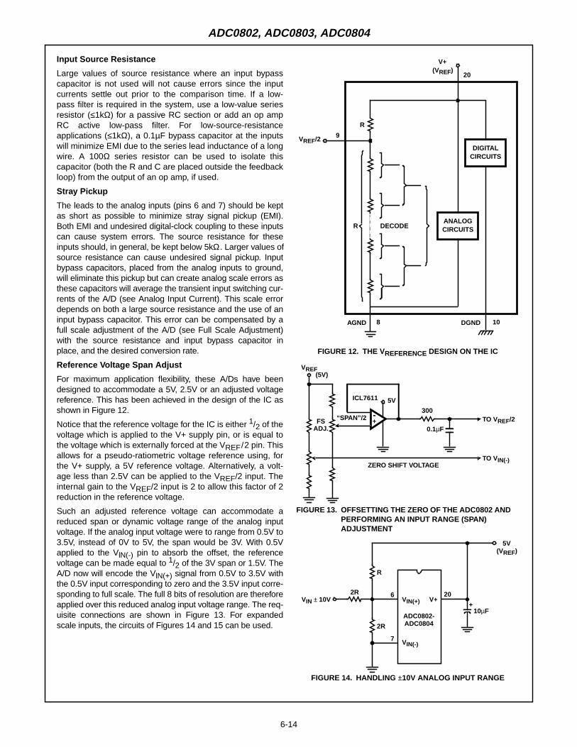
6-14
Input Source Resistance
Large values of source resistance where an input bypasscapacitor is not used will not cause errors since the inputcurrents settle out prior to the comparison time. If a low-pass filter is required in the system, use a low-value seriesresistor (≤1kΩ) for a passive RC section or add an op ampRC active low-pass filter. For low-source-resistanceapplications (≤1kΩ), a 0.1µF bypass capacitor at the inputswill minimize EMI due to the series lead inductance of a longwire. A 100Ω series resistor can be used to isolate thiscapacitor (both the R and C are placed outside the feedbackloop) from the output of an op amp, if used.
Stray Pickup
The leads to the analog inputs (pins 6 and 7) should be keptas short as possible to minimize stray signal pickup (EMI).Both EMI and undesired digital-clock coupling to these inputscan cause system errors. The source resistance for theseinputs should, in general, be kept below 5kΩ. Larger values ofsource resistance can cause undesired signal pickup. Inputbypass capacitors, placed from the analog inputs to ground,will eliminate this pickup but can create analog scale errors asthese capacitors will average the transient input switching cur-rents of the A/D (see Analog Input Current). This scale errordepends on both a large source resistance and the use of aninput bypass capacitor. This error can be compensated by afull scale adjustment of the A/D (see Full Scale Adjustment)with the source resistance and input bypass capacitor inplace, and the desired conversion rate.
Reference Voltage Span Adjust
For maximum application flexibility, these A/Ds have beendesigned to accommodate a 5V, 2.5V or an adjusted voltagereference. This has been achieved in the design of the IC asshown in Figure 12.
Notice that the reference voltage for the IC is either 1/2 of thevoltage which is applied to the V+ supply pin, or is equal tothe voltage which is externally forced at the VREF/2 pin. Thisallows for a pseudo-ratiometric voltage reference using, forthe V+ supply, a 5V reference voltage. Alternatively, a volt-age less than 2.5V can be applied to the VREF/2 input. Theinternal gain to the VREF/2 input is 2 to allow this factor of 2reduction in the reference voltage.
Such an adjusted reference voltage can accommodate areduced span or dynamic voltage range of the analog inputvoltage. If the analog input voltage were to range from 0.5V to3.5V, instead of 0V to 5V, the span would be 3V. With 0.5Vapplied to the VlN(-) pin to absorb the offset, the referencevoltage can be made equal to 1/2 of the 3V span or 1.5V. TheA/D now will encode the VlN(+) signal from 0.5V to 3.5V withthe 0.5V input corresponding to zero and the 3.5V input corre-sponding to full scale. The full 8 bits of resolution are thereforeapplied over this reduced analog input voltage range. The req-uisite connections are shown in Figure 13. For expandedscale inputs, the circuits of Figures 14 and 15 can be used.
FIGURE 12. THE VREFERENCE DESIGN ON THE IC
FIGURE 13. OFFSETTING THE ZERO OF THE ADC0802 ANDPERFORMING AN INPUT RANGE (SPAN)ADJUSTMENT
FIGURE 14. HANDLING ±10V ANALOG INPUT RANGE
V+
DGND
VREF/2
AGND
(VREF)
R
R
DIGITALCIRCUITS
ANALOGCIRCUITS
9
8 10
20
DECODE
300TO VREF/2
TO VIN(-)ZERO SHIFT VOLTAGE
0.1µF
5V
-+
VREF(5V)
FSADJ.
“SPAN”/2
ICL7611
VIN(-)
2R
5V
2R
VIN ± 10V
R
VIN(+)
(VREF)
V+20
10µF
6
7
+
ADC0802-ADC0804
ADC0802, ADC0803, ADC0804
6-15
Reference Accuracy Requirements
The converter can be operated in a pseudo-ratiometricmode or an absolute mode. In ratiometric converter applica-tions, the magnitude of the reference voltage is a factor inboth the output of the source transducer and the output ofthe A/D converter and therefore cancels out in the final digi-tal output code. In absolute conversion applicatIons, both theinitial value and the temperature stability of the referencevoltage are important accuracy factors in the operation of theA/D converter. For VREF/2 voltages of 2.5V nominal value,initial errors of ±10mV will cause conversion errors of ±1LSB due to the gain of 2 of the VREF/2 input. In reducedspan applications, the initial value and the stability of theVREF/2 input voltage become even more important. Forexample, if the span is reduced to 2.5V, the analog input LSBvoltage value is correspondingly reduced from 20mV (5Vspan) to 10mV and 1 LSB at the VREF/2 input becomes5mV. As can be seen, this reduces the allowed initial toler-ance of the reference voltage and requires correspondinglyless absolute change with temperature variations. Note thatspans smaller than 2.5V place even tighter requirements onthe initial accuracy and stability of the reference source.
In general, the reference voltage will require an initialadjustment. Errors due to an improper value of referencevoltage appear as full scale errors in the A/D transfer func-tion. IC voltage regulators may be used for references if theambient temperature changes are not excessive.
Zero Error
The zero of the A/D does not require adjustment. If theminimum analog input voltage value, VlN(MlN), is not ground, azero offset can be done. The converter can be made to output0000 0000 digital code for this minimum input voltage by bias-ing the A/D VIN(-) input at this VlN(MlN) value (see Applicationssection). This utilizes the differential mode operation of the A/D.
The zero error of the A/D converter relates to the location ofthe first riser of the transfer function and can be measured bygrounding the VIN(-) input and applying a small magnitudepositive voltage to the VIN(+) input. Zero error is the differencebetween the actual DC input voltage which is necessary tojust cause an output digital code transition from 0000 0000 to0000 0001 and the ideal 1/2 LSB value (1/2 LSB = 9.8mV forVREF/2 = 2.500V).
Full Scale Adjust
The full scale adjustment can be made by applying adifferential input voltage which is 11/2 LSB down from thedesired analog full scale voltage range and then adjustingthe magnitude of the VREF/2 input (pin 9) for a digital outputcode which is just changing from 1111 1110 to 1111 1111.When offsetting the zero and using a span-adjusted VREF/2voltage, the full scale adjustment is made by inputting VMlNto the VIN(-) input of the A/D and applying a voltage to theVIN(+) input which is given by:
,
where:
VMAX = the high end of the analog input range,
and
VMIN = the low end (the offset zero) of the analog range.(Both are ground referenced.)
Clocking Option
The clock for the A/D can be derived from an external sourcesuch as the CPU clock or an external RC network can beadded to provIde self-clocking. The CLK IN (pin 4) makesuse of a Schmitt trigger as shown in Figure 16.
Heavy capacitive or DC loading of the CLK R pin should beavoided as this will disturb normal converter operation.Loads less than 50pF, such as driving up to 7 A/D converterclock inputs from a single CLK R pin of 1 converter, areallowed. For larger clock line loading, a CMOS or low powerTTL buffer or PNP input logic should be used to minimize theloading on the CLK R pin (do not use a standard TTL buffer).
Restart During a Conversion
If the A/D is restarted (CS and WR go low and return high)during a conversion, the converter is reset and a new con-version is started. The output data latch is not updated if theconversion in progress is not completed. The data from theprevious conversion remain in this latch.
Continuous Conversions
In this application, the CS input is grounded and the WRinput is tied to the INTR output. This WR and INTR nodeshould be momentarily forced to logic low following a power-up cycle to insure circuit operation. See Figure 17 for details.
FIGURE 15. HANDLING ±5V ANALOG INPUT RANGE
VIN(-)
R
5V
VIN ±5V
R
VIN(+)
(VREF)
V+20
10µF
6
7
+
ADC0802-ADC0804
VIN +( )fSADJ VMAX 1.5VMAX VMIN–( )
256-----------------------------------------–=
CLK R
4CLK IN
CLK
ADC0802-ADC0804
fCLK ≅
19
R
C
11.1 RC
R ≅ 10kΩ
FIGURE 16. SELF-CLOCKING THE A/D
ADC0802, ADC0803, ADC0804
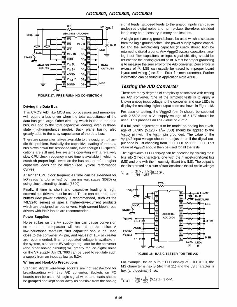
6-16
Driving the Data Bus
This CMOS A/D, like MOS microprocessors and memories,will require a bus driver when the total capacitance of thedata bus gets large. Other circuItry, which is tied to the databus, will add to the total capacitive loading, even in three-state (high-impedance mode). Back plane busing alsogreatly adds to the stray capacitance of the data bus.
There are some alternatives available to the designer to han-dle this problem. Basically, the capacitive loading of the databus slows down the response time, even though DC specifi-cations are still met. For systems operating with a relativelyslow CPU clock frequency, more time is available in which toestablish proper logic levels on the bus and therefore highercapacitive loads can be driven (see Typical PerformanceCurves).
At higher CPU clock frequencies time can be extended forI/O reads (and/or writes) by inserting wait states (8080) orusing clock-extending circuits (6800).
Finally, if time is short and capacitive loading is high,external bus drivers must be used. These can be three-statebuffers (low power Schottky is recommended, such as the74LS240 series) or special higher-drive-current productswhich are designed as bus drivers. High-current bipolar busdrivers with PNP inputs are recommended.
Power Supplies
Noise spikes on the V+ supply line can cause conversionerrors as the comparator will respond to this noise. Alow-inductance tantalum filter capacitor should be usedclose to the converter V+ pin, and values of 1µF or greaterare recommended. If an unregulated voltage is available inthe system, a separate 5V voltage regulator for the converter(and other analog circuitry) will greatly reduce digital noiseon the V+ supply. An lCL7663 can be used to regulate sucha supply from an input as low as 5.2V.
Wiring and Hook-Up Precautions
Standard digital wire-wrap sockets are not satisfactory forbreadboarding with this A/D converter. Sockets on PCboards can be used. All logic signal wires and leads shouldbe grouped and kept as far away as possible from the analog
signal leads. Exposed leads to the analog inputs can causeundesired digital noise and hum pickup; therefore, shieldedleads may be necessary in many applications.
A single-point analog ground should be used which is separatefrom the logic ground points. The power supply bypass capaci-tor and the self-clockIng capacitor (if used) should both bereturned to digital ground. Any VREF/2 bypass capacitors, ana-log input filter capacitors, or input signal shielding should bereturned to the analog ground point. A test for proper groundingis to measure the zero error of the A/D converter. Zero errors inexcess of 1/4 LSB can usually be traced to improper boardlayout and wiring (see Zero Error for measurement). Furtherinformation can be found in Application Note AN018.
Testing the A/D ConverterThere are many degrees of complexity associated with testingan A/D converter. One of the simplest tests is to apply aknown analog input voltage to the converter and use LEDs todisplay the resulting digital output code as shown in Figure 18.
For ease of testing, the VREF/2 (pin 9) should be suppliedwith 2.560V and a V+ supply voltage of 5.12V should beused. This provides an LSB value of 20mV.
If a full scale adjustment is to be made, an analog input volt-age of 5.090V (5.120 - 11/2 LSB) should be applied to theVIN(+) pin with the VIN(-) pin grounded. The value of theVREF/2 input voltage should be adjusted until the digital out-put code is just changing from 1111 1110 to 1111 1111. Thisvalue of VREF/2 should then be used for all the tests.
The digital-output LED display can be decoded by dividing the 8bits into 2 hex characters, one with the 4 most-significant bits(MS) and one with the 4 least-significant bits (LS). The output isthen interpreted as a sum of fractions times the full scale voltage:
.
For example, for an output LED display of 1011 0110, theMS character is hex B (decimal 11) and the LS character ishex (and decimal) 6, so:
.
11
12
13
14
15
16
17
18
20
19
10
9
8
7
6
5
4
3
2
1
ADC0802 - ADC0804
WR
RD
CS
INTR
CLK IN
VIN (-)
VIN (+)
DGND
VREF/2
AGND
DB1
DB0
DB4
DB3
DB2
DB7
DB6
DB5
CLK R
V+
10K 5V (VREF)
10µF+
DATA
START
ANALOGINPUTS
150pF
OUTPUTS
N.O.
MSB
LSB
FIGURE 17. FREE-RUNNING CONNECTION
VOUTMS16--------- LS
256----------+
5.12( )V=
START
VIN (+)
DGND
2.560VAGND
10µF
150pF
N.O.
0.1µF
0.1µF
TANTALUM
5.120V
5V
1.3kΩ LEDs(8) (8)
MSB
LSB
10kΩ
VREF/2
+
11
12
13
14
15
16
17
18
20
19
10
9
8
7
6
5
4
3
2
1
ADC0802-ADC0804
FIGURE 18. BASIC TESTER FOR THE A/D
VOUT1116------ 6
256----------+
5.12( ) 3.64V= =
ADC0802, ADC0803, ADC0804
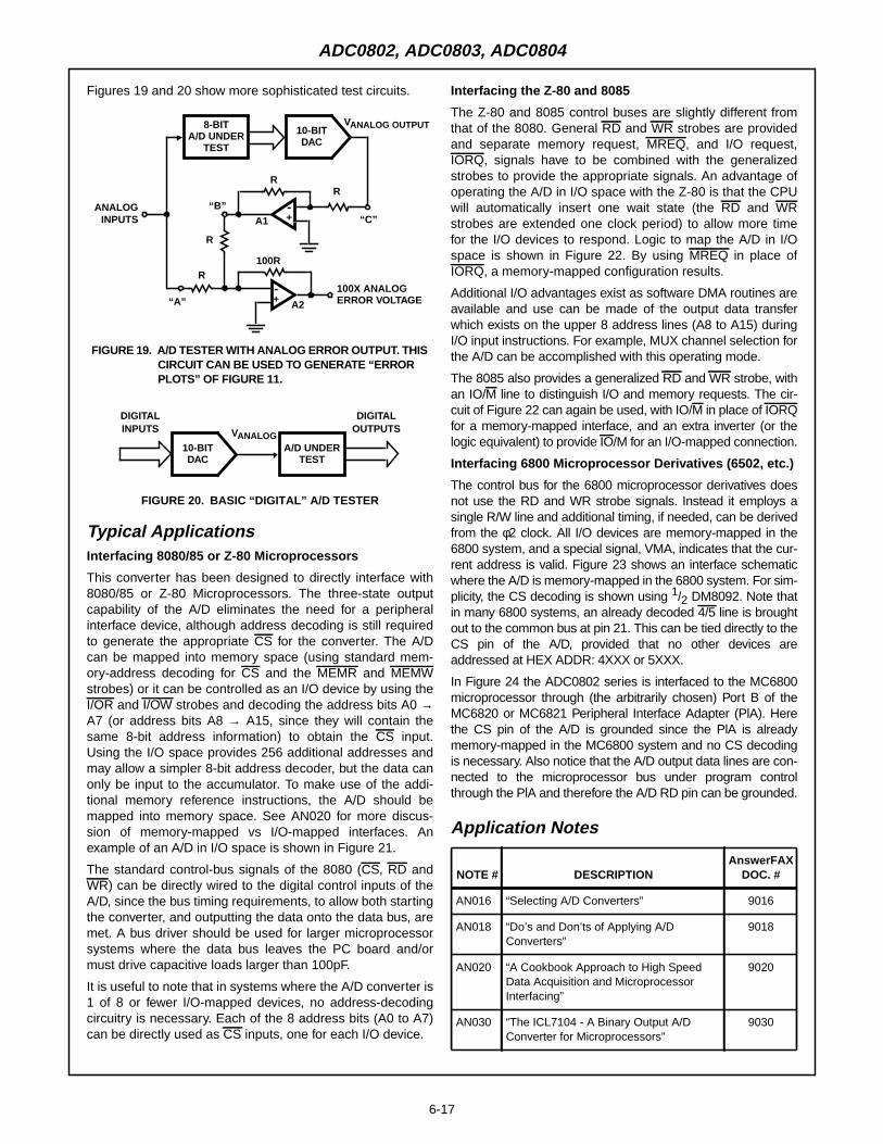
6-17
Figures 19 and 20 show more sophisticated test circuits.
Typical ApplicationsInterfacing 8080/85 or Z-80 Microprocessors
This converter has been designed to directly interface with8080/85 or Z-80 Microprocessors. The three-state outputcapability of the A/D eliminates the need for a peripheralinterface device, although address decoding is still requiredto generate the appropriate CS for the converter. The A/Dcan be mapped into memory space (using standard mem-ory-address decoding for CS and the MEMR and MEMWstrobes) or it can be controlled as an I/O device by using theI/OR and I/OW strobes and decoding the address bits A0 →A7 (or address bits A8 → A15, since they will contain thesame 8-bit address information) to obtain the CS input.Using the I/O space provides 256 additional addresses andmay allow a simpler 8-bit address decoder, but the data canonly be input to the accumulator. To make use of the addi-tional memory reference instructions, the A/D should bemapped into memory space. See AN020 for more discus-sion of memory-mapped vs I/O-mapped interfaces. Anexample of an A/D in I/O space is shown in Figure 21.
The standard control-bus signals of the 8080 (CS, RD andWR) can be directly wired to the digital control inputs of theA/D, since the bus timing requirements, to allow both startingthe converter, and outputting the data onto the data bus, aremet. A bus driver should be used for larger microprocessorsystems where the data bus leaves the PC board and/ormust drive capacitive loads larger than 100pF.
It is useful to note that in systems where the A/D converter is1 of 8 or fewer I/O-mapped devices, no address-decodingcircuitry is necessary. Each of the 8 address bits (A0 to A7)can be directly used as CS inputs, one for each I/O device.
Interfacing the Z-80 and 8085
The Z-80 and 8085 control buses are slightly different fromthat of the 8080. General RD and WR strobes are providedand separate memory request, MREQ, and I/O request,IORQ, signals have to be combined with the generalizedstrobes to provide the appropriate signals. An advantage ofoperating the A/D in I/O space with the Z-80 is that the CPUwill automatically insert one wait state (the RD and WRstrobes are extended one clock period) to allow more timefor the I/O devices to respond. Logic to map the A/D in I/Ospace is shown in Figure 22. By using MREQ in place ofIORQ, a memory-mapped configuration results.
Additional I/O advantages exist as software DMA routines areavailable and use can be made of the output data transferwhich exists on the upper 8 address lines (A8 to A15) duringI/O input instructions. For example, MUX channel selection forthe A/D can be accomplished with this operating mode.
The 8085 also provides a generalized RD and WR strobe, withan IO/M line to distinguish I/O and memory requests. The cir-cuit of Figure 22 can again be used, with IO/M in place of IORQfor a memory-mapped interface, and an extra inverter (or thelogic equivalent) to provide IO/M for an I/O-mapped connection.
Interfacing 6800 Microprocessor Derivatives (6502, etc.)
The control bus for the 6800 microprocessor derivatives doesnot use the RD and WR strobe signals. Instead it employs asingle R/W line and additional timing, if needed, can be derivedfrom the φ2 clock. All I/O devices are memory-mapped in the6800 system, and a special signal, VMA, indicates that the cur-rent address is valid. Figure 23 shows an interface schematicwhere the A/D is memory-mapped in the 6800 system. For sim-plicity, the CS decoding is shown using 1/2 DM8092. Note thatin many 6800 systems, an already decoded 4/5 line is broughtout to the common bus at pin 21. This can be tied directly to theCS pin of the A/D, provided that no other devices areaddressed at HEX ADDR: 4XXX or 5XXX.
In Figure 24 the ADC0802 series is interfaced to the MC6800microprocessor through (the arbitrarily chosen) Port B of theMC6820 or MC6821 Peripheral Interface Adapter (PlA). Herethe CS pin of the A/D is grounded since the PlA is alreadymemory-mapped in the MC6800 system and no CS decodingis necessary. Also notice that the A/D output data lines are con-nected to the microprocessor bus under program controlthrough the PlA and therefore the A/D RD pin can be grounded.
Application Notes
ANALOGINPUTS
“A”
R
“B”
R
RR
“C”
100R
-+ A2
8-BITA/D UNDER
TEST
10-BITDAC
VANALOG OUTPUT
100X ANALOG
-+A1
ERROR VOLTAGE
FIGURE 19. A/D TESTER WITH ANALOG ERROR OUTPUT. THISCIRCUIT CAN BE USED TO GENERATE “ERRORPLOTS” OF FIGURE 11.
A/D UNDERTEST
10-BITDAC
DIGITAL
VANALOGINPUTS
DIGITALOUTPUTS
FIGURE 20. BASIC “DIGITAL” A/D TESTER
NOTE # DESCRIPTIONAnswerFAX
DOC. #
AN016 “Selecting A/D Converters” 9016
AN018 “Do’s and Don’ts of Applying A/DConverters”
9018
AN020 “A Cookbook Approach to High SpeedData Acquisition and MicroprocessorInterfacing”
9020
AN030 “The ICL7104 - A Binary Output A/DConverter for Microprocessors”
9030
ADC0802, ADC0803, ADC0804
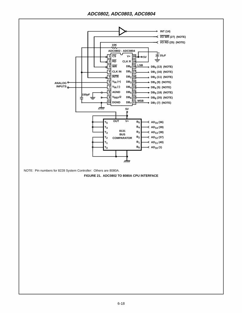
6-18
NOTE: Pin numbers for 8228 System Controller: Others are 8080A.
FIGURE 21. ADC0802 TO 8080A CPU INTERFACE
11
12
13
14
15
16
17
18
20
19
10
9
8
7
6
5
4
3
2
1
ADC0802 - ADC0804
WR
RD
CS
INTR
CLK IN
VIN (-)
VIN (+)
DGND
VREF/2
AGND
DB1
DB0
DB4
DB3
DB2
DB7
DB6
DB5
CLK R
V+
10K
5V 10µF+
ANALOGINPUTS
150pF
MSB
LSB
DB1 (16) (NOTE)
DB0 (13) (NOTE)
DB4 (5) (NOTE)
DB3 (9) (NOTE)
DB2 (11) (NOTE)
DB7 (7) (NOTE)
DB6 (20) (NOTE)
DB5 (18) (NOTE)
5V
AD15 (36)
AD14 (39)
AD13 (38)
AD12 (37)
AD11 (40)
AD10 (1)
8131BUS
COMPARATOR
INT (14)
I/O RD (25) (NOTE)
I/O WR (27) (NOTE)
T5
T4
T3
T2
T1
T0
B5
B4
B3
B2
B1
B0
V+OUT
ADC0802, ADC0803, ADC0804
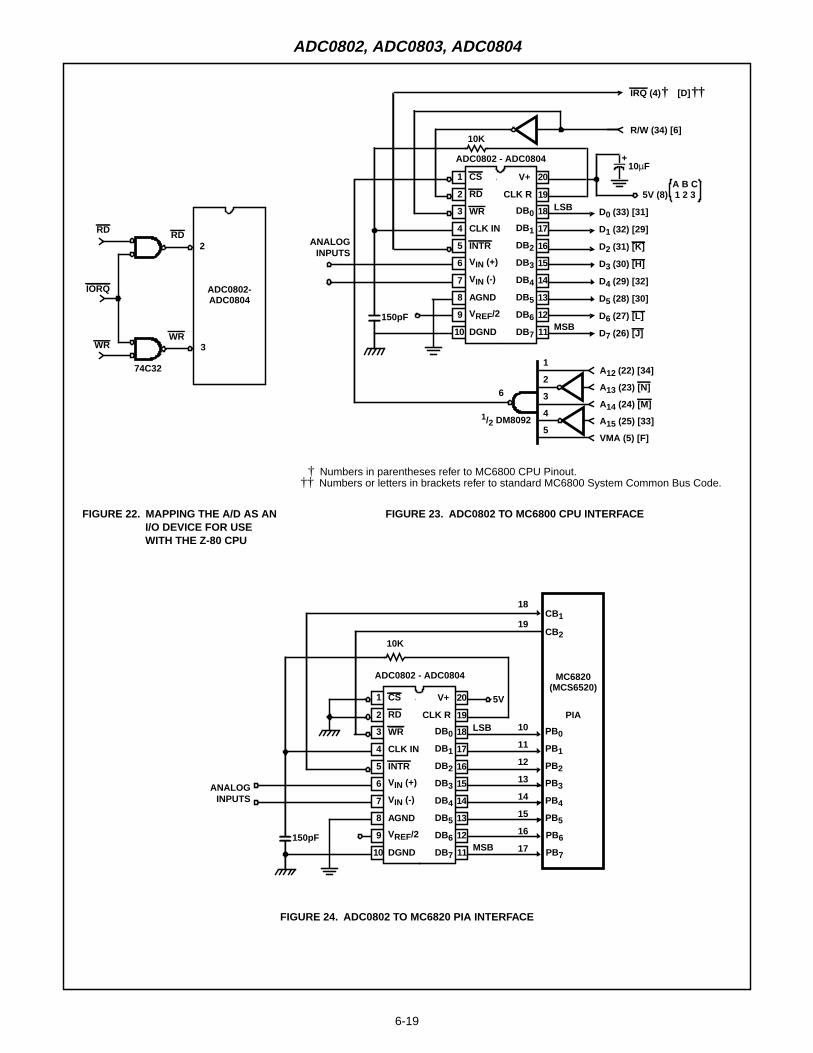
6-19
FIGURE 22. MAPPING THE A/D AS ANI/O DEVICE FOR USEWITH THE Z-80 CPU
FIGURE 23. ADC0802 TO MC6800 CPU INTERFACE
FIGURE 24. ADC0802 TO MC6820 PIA INTERFACE
WR
RD
IORQ
RD
WR
74C32
ADC0802-ADC0804
3
2
11
12
13
14
15
16
17
18
20
19
10
9
8
7
6
5
4
3
2
1
ADC0802 - ADC0804
WR
RD
CS
INTR
CLK IN
VIN (-)
VIN (+)
DGND
VREF/2
AGND
DB1
DB0
DB4
DB3
DB2
DB7
DB6
DB5
CLK R
V+
10K
5V (8)
10µF+
ANALOGINPUTS
150pFMSB
LSB
D1 (32) [29]
D0 (33) [31]
D4 (29) [32]
D3 (30) [H]
D2 (31) [K]
D7 (26) [J]
D6 (27) [L]
D5 (28) [30]
A12 (22) [34]
A13 (23) [N]
A14 (24) [M]
A15 (25) [33]
VMA (5) [F]
IRQ (4)† [D] ††
R/W (34) [6]
1
2
3
4
5
6
1/2 DM8092
A B C1 2 3
† Numbers in parentheses refer to MC6800 CPU Pinout.†† Numbers or letters in brackets refer to standard MC6800 System Common Bus Code.
11
12
13
14
15
16
17
18
20
19
10
9
8
7
6
5
4
3
2
1
ADC0802 - ADC0804
WR
RD
CS
INTR
CLK IN
VIN (-)
VIN (+)
DGND
VREF/2
AGND
DB1
DB0
DB4
DB3
DB2
DB7
DB6
DB5
CLK R
V+
10K
5V
ANALOGINPUTS
150pFMSB
LSB
11
10
14
13
12
17
16
15
PB1
PB0
PB4
PB3
PB2
PB7
PB6
PB5
MC6820(MCS6520)
PIA
CB2
CB119
18
ADC0802, ADC0803, ADC0804
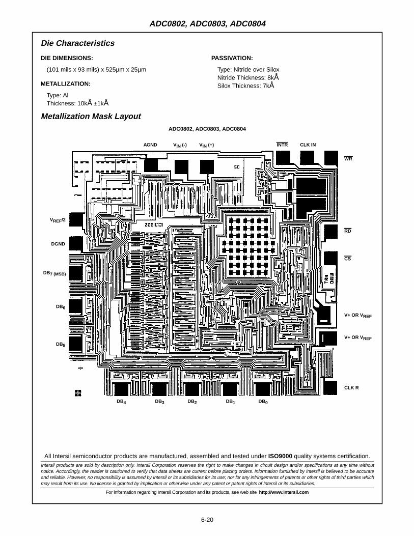
6-20
Die Characteristics
DIE DIMENSIONS:
(101 mils x 93 mils) x 525µm x 25µm
METALLIZATION:
Type: AlThickness: 10kÅ ±1kÅ
PASSIVATION:
Type: Nitride over SiloxNitride Thickness: 8kÅSilox Thickness: 7kÅ
Metallization Mask LayoutADC0802, ADC0803, ADC0804
WR
RD
CS
CLK ININTRVIN (-) VIN (+)
DGND
VREF/2
AGND
V+ OR VREF
CLK R
DB0DB1DB2DB3DB4
DB5
DB6
DB7 (MSB)
V+ OR VREF
ADC0802, ADC0803, ADC0804
All Intersil semiconductor products are manufactured, assembled and tested under ISO9000 quality systems certification.Intersil products are sold by description only. Intersil Corporation reserves the right to make changes in circuit design and/or specifications at any time withoutnotice. Accordingly, the reader is cautioned to verify that data sheets are current before placing orders. Information furnished by Intersil is believed to be accurateand reliable. However, no responsibility is assumed by Intersil or its subsidiaries for its use; nor for any infringements of patents or other rights of third parties whichmay result from its use. No license is granted by implication or otherwise under any patent or patent rights of Intersil or its subsidiaries.
For information regarding Intersil Corporation and its products, see web site http://www.intersil.com
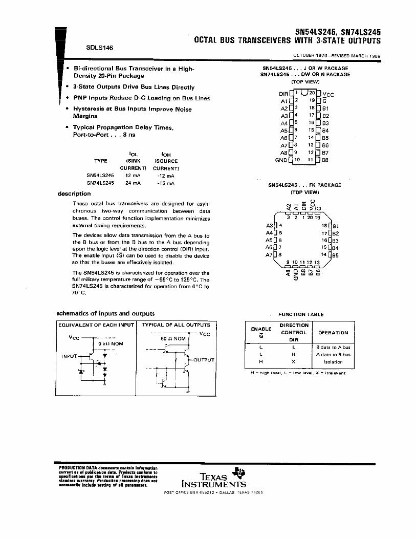
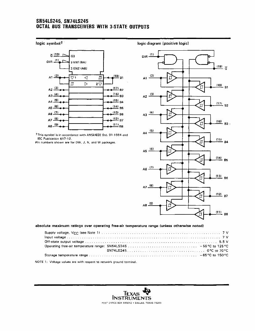
IMPORTANT NOTICE
Texas Instruments (TI) reserves the right to make changes to its products or to discontinue any semiconductorproduct or service without notice, and advises its customers to obtain the latest version of relevant informationto verify, before placing orders, that the information being relied on is current.
TI warrants performance of its semiconductor products and related software to the specifications applicable atthe time of sale in accordance with TI’s standard warranty. Testing and other quality control techniques areutilized to the extent TI deems necessary to support this warranty. Specific testing of all parameters of eachdevice is not necessarily performed, except those mandated by government requirements.
Certain applications using semiconductor products may involve potential risks of death, personal injury, orsevere property or environmental damage (“Critical Applications”).
TI SEMICONDUCTOR PRODUCTS ARE NOT DESIGNED, INTENDED, AUTHORIZED, OR WARRANTEDTO BE SUITABLE FOR USE IN LIFE-SUPPORT APPLICATIONS, DEVICES OR SYSTEMS OR OTHERCRITICAL APPLICATIONS.
Inclusion of TI products in such applications is understood to be fully at the risk of the customer. Use of TIproducts in such applications requires the written approval of an appropriate TI officer. Questions concerningpotential risk applications should be directed to TI through a local SC sales office.
In order to minimize risks associated with the customer’s applications, adequate design and operatingsafeguards should be provided by the customer to minimize inherent or procedural hazards.
TI assumes no liability for applications assistance, customer product design, software performance, orinfringement of patents or services described herein. Nor does TI warrant or represent that any license, eitherexpress or implied, is granted under any patent right, copyright, mask work right, or other intellectual propertyright of TI covering or relating to any combination, machine, or process in which such semiconductor productsor services might be or are used.
Copyright 1996, Texas Instruments Incorporated

IMPORTANT NOTICE
Texas Instruments and its subsidiaries (TI) reserve the right to make changes to their products or to discontinueany product or service without notice, and advise customers to obtain the latest version of relevant informationto verify, before placing orders, that information being relied on is current and complete. All products are soldsubject to the terms and conditions of sale supplied at the time of order acknowledgement, including thosepertaining to warranty, patent infringement, and limitation of liability.
TI warrants performance of its semiconductor products to the specifications applicable at the time of sale inaccordance with TI’s standard warranty. Testing and other quality control techniques are utilized to the extentTI deems necessary to support this warranty. Specific testing of all parameters of each device is not necessarilyperformed, except those mandated by government requirements.
CERTAIN APPLICATIONS USING SEMICONDUCTOR PRODUCTS MAY INVOLVE POTENTIAL RISKS OFDEATH, PERSONAL INJURY, OR SEVERE PROPERTY OR ENVIRONMENTAL DAMAGE (“CRITICALAPPLICATIONS”). TI SEMICONDUCTOR PRODUCTS ARE NOT DESIGNED, AUTHORIZED, ORWARRANTED TO BE SUITABLE FOR USE IN LIFE-SUPPORT DEVICES OR SYSTEMS OR OTHERCRITICAL APPLICATIONS. INCLUSION OF TI PRODUCTS IN SUCH APPLICATIONS IS UNDERSTOOD TOBE FULLY AT THE CUSTOMER’S RISK.
In order to minimize risks associated with the customer’s applications, adequate design and operatingsafeguards must be provided by the customer to minimize inherent or procedural hazards.
TI assumes no liability for applications assistance or customer product design. TI does not warrant or representthat any license, either express or implied, is granted under any patent right, copyright, mask work right, or otherintellectual property right of TI covering or relating to any combination, machine, or process in which suchsemiconductor products or services might be or are used. TI’s publication of information regarding any thirdparty’s products or services does not constitute TI’s approval, warranty or endorsement thereof.
Copyright 1998, Texas Instruments Incorporated
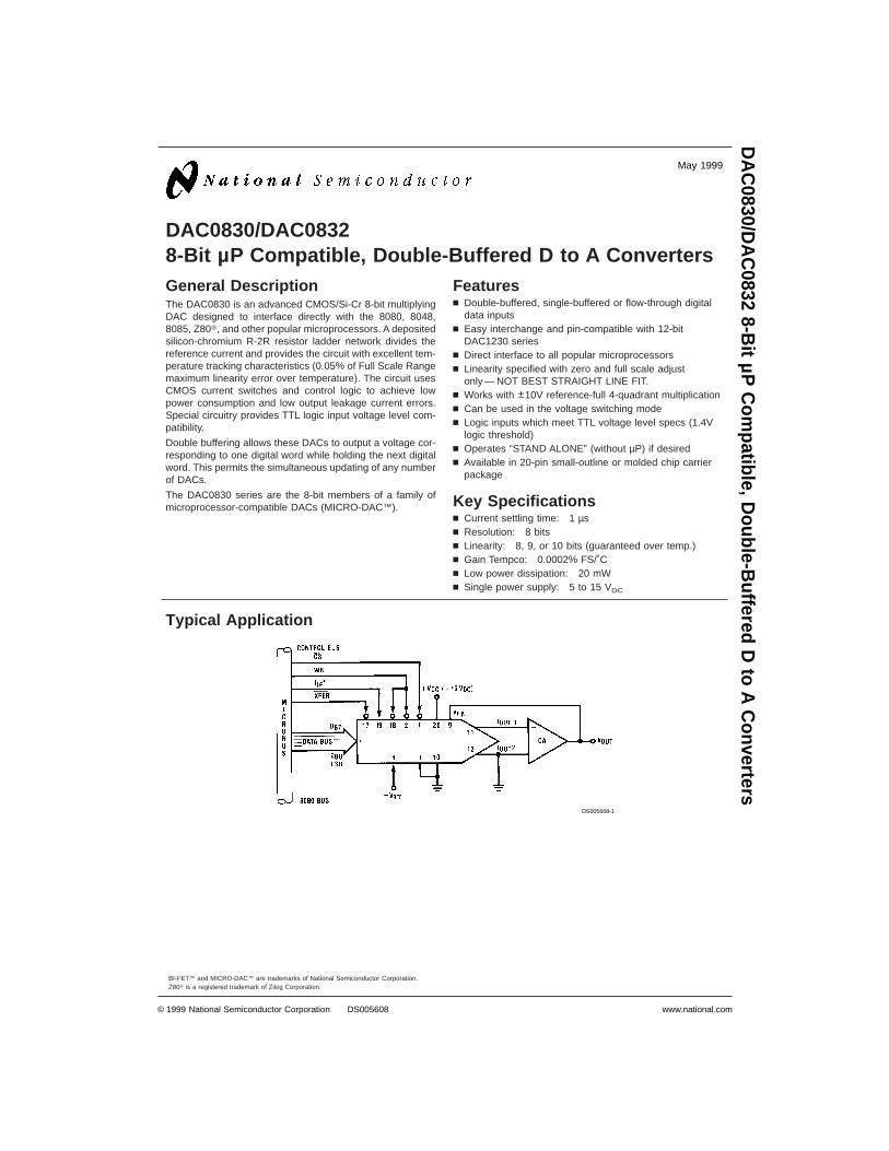
DAC0830/DAC08328-Bit µP Compatible, Double-Buffered D to A ConvertersGeneral DescriptionThe DAC0830 is an advanced CMOS/Si-Cr 8-bit multiplyingDAC designed to interface directly with the 8080, 8048,8085, Z80®, and other popular microprocessors. A depositedsilicon-chromium R-2R resistor ladder network divides thereference current and provides the circuit with excellent tem-perature tracking characteristics (0.05% of Full Scale Rangemaximum linearity error over temperature). The circuit usesCMOS current switches and control logic to achieve lowpower consumption and low output leakage current errors.Special circuitry provides TTL logic input voltage level com-patibility.
Double buffering allows these DACs to output a voltage cor-responding to one digital word while holding the next digitalword. This permits the simultaneous updating of any numberof DACs.
The DAC0830 series are the 8-bit members of a family ofmicroprocessor-compatible DACs (MICRO-DAC™).
Featuresn Double-buffered, single-buffered or flow-through digital
data inputsn Easy interchange and pin-compatible with 12-bit
DAC1230 seriesn Direct interface to all popular microprocessorsn Linearity specified with zero and full scale adjust
only — NOT BEST STRAIGHT LINE FIT.n Works with ±10V reference-full 4-quadrant multiplicationn Can be used in the voltage switching moden Logic inputs which meet TTL voltage level specs (1.4V
logic threshold)n Operates “STAND ALONE” (without µP) if desiredn Available in 20-pin small-outline or molded chip carrier
package
Key Specificationsn Current settling time: 1 µsn Resolution: 8 bitsn Linearity: 8, 9, or 10 bits (guaranteed over temp.)n Gain Tempco: 0.0002% FS/˚Cn Low power dissipation: 20 mWn Single power supply: 5 to 15 VDC
Typical Application
BI-FET™ and MICRO-DAC™ are trademarks of National Semiconductor Corporation.Z80® is a registered trademark of Zilog Corporation.
DS005608-1
May 1999
DA
C0830/D
AC
08328-B
itµPC
ompatible,D
ouble-Buffered
Dto
AC
onverters
© 1999 National Semiconductor Corporation DS005608 www.national.com
Connection Diagrams (Top Views)
Dual-In-Line andSmall-Outline Packages
DS005608-21
Molded Chip Carrier Package
DS005608-22
www.national.com 2
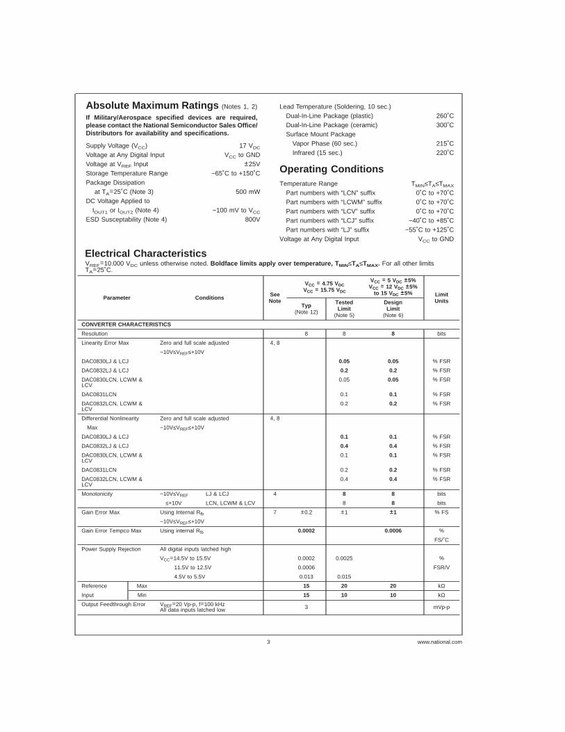
Absolute Maximum Ratings (Notes 1, 2)
If Military/Aerospace specified devices are required,please contact the National Semiconductor Sales Office/Distributors for availability and specifications.
Supply Voltage (VCC) 17 VDC
Voltage at Any Digital Input VCC to GNDVoltage at VREF Input ±25VStorage Temperature Range −65˚C to +150˚CPackage Dissipation
at TA=25˚C (Note 3) 500 mWDC Voltage Applied to
IOUT1 or IOUT2 (Note 4) −100 mV to VCC
ESD Susceptability (Note 4) 800V
Lead Temperature (Soldering, 10 sec.)Dual-In-Line Package (plastic) 260˚CDual-In-Line Package (ceramic) 300˚CSurface Mount Package
Vapor Phase (60 sec.) 215˚CInfrared (15 sec.) 220˚C
Operating ConditionsTemperature Range TMIN≤TA≤TMAX
Part numbers with “LCN” suffix 0˚C to +70˚CPart numbers with “LCWM” suffix 0˚C to +70˚CPart numbers with “LCV” suffix 0˚C to +70˚CPart numbers with “LCJ” suffix −40˚C to +85˚CPart numbers with “LJ” suffix −55˚C to +125˚C
Voltage at Any Digital Input VCC to GND
Electrical CharacteristicsVREF=10.000 VDC unless otherwise noted. Boldface limits apply over temperature, T MIN≤TA≤TMAX. For all other limitsTA=25˚C.
Parameter Conditions SeeNote
VCC = 4.75 VDCVCC = 15.75 VDC
VCC = 5 VDC ±5%VCC = 12 VDC ±5%
to 15 VDC ±5% LimitUnits
Typ(Note 12)
TestedLimit
(Note 5)
DesignLimit
(Note 6)
CONVERTER CHARACTERISTICS
Resolution 8 8 8 bits
Linearity Error Max Zero and full scale adjusted 4, 8
−10V≤VREF≤+10V
DAC0830LJ & LCJ 0.05 0.05 % FSR
DAC0832LJ & LCJ 0.2 0.2 % FSR
DAC0830LCN, LCWM &LCV
0.05 0.05 % FSR
DAC0831LCN 0.1 0.1 % FSR
DAC0832LCN, LCWM &LCV
0.2 0.2 % FSR
Differential Nonlinearity Zero and full scale adjusted 4, 8
Max −10V≤VREF≤+10V
DAC0830LJ & LCJ 0.1 0.1 % FSR
DAC0832LJ & LCJ 0.4 0.4 % FSR
DAC0830LCN, LCWM &LCV
0.1 0.1 % FSR
DAC0831LCN 0.2 0.2 % FSR
DAC0832LCN, LCWM &LCV
0.4 0.4 % FSR
Monotonicity −10V≤VREF LJ & LCJ 4 8 8 bits
≤+10V LCN, LCWM & LCV 8 8 bits
Gain Error Max Using Internal Rfb 7 ±0.2 ±1 ±1 % FS
−10V≤VREF≤+10V
Gain Error Tempco Max Using internal Rfb 0.0002 0.0006 %
FS/˚C
Power Supply Rejection All digital inputs latched high
VCC=14.5V to 15.5V 0.0002 0.0025 %
11.5V to 12.5V 0.0006 FSR/V
4.5V to 5.5V 0.013 0.015
Reference Max 15 20 20 kΩ
Input Min 15 10 10 kΩ
Output Feedthrough Error VREF=20 Vp-p, f=100 kHzAll data inputs latched low 3 mVp-p
www.national.com3
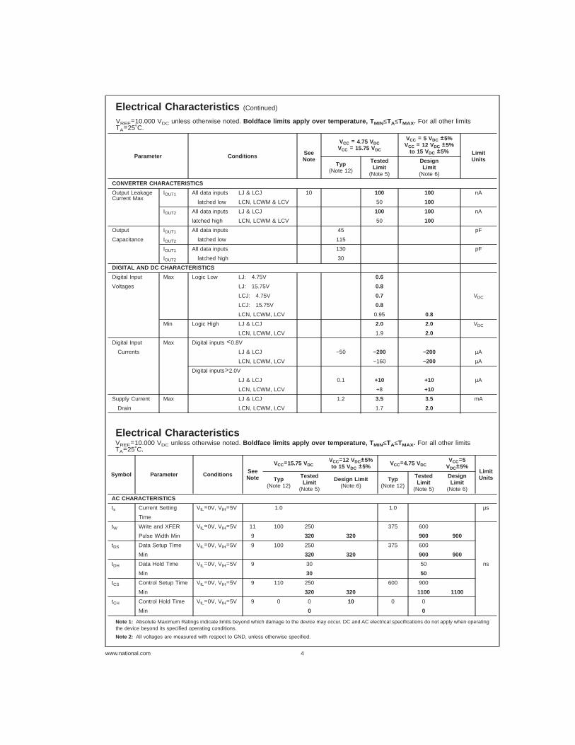
Electrical Characteristics (Continued)
VREF=10.000 VDC unless otherwise noted. Boldface limits apply over temperature, T MIN≤TA≤TMAX. For all other limitsTA=25˚C.
Parameter Conditions SeeNote
VCC = 4.75 VDCVCC = 15.75 VDC
VCC = 5 VDC ±5%VCC = 12 VDC ±5%
to 15 VDC ±5% LimitUnits
Typ(Note 12)
TestedLimit
(Note 5)
DesignLimit
(Note 6)
CONVERTER CHARACTERISTICS
Output LeakageCurrent Max
IOUT1 All data inputs LJ & LCJ 10 100 100 nA
latched low LCN, LCWM & LCV 50 100
IOUT2 All data inputs LJ & LCJ 100 100 nA
latched high LCN, LCWM & LCV 50 100
Output IOUT1 All data inputs 45 pF
Capacitance IOUT2 latched low 115
IOUT1 All data inputs 130 pF
IOUT2 latched high 30
DIGITAL AND DC CHARACTERISTICS
Digital Input Max Logic Low LJ: 4.75V 0.6
Voltages LJ: 15.75V 0.8
LCJ: 4.75V 0.7 VDC
LCJ: 15.75V 0.8
LCN, LCWM, LCV 0.95 0.8
Min Logic High LJ & LCJ 2.0 2.0 VDC
LCN, LCWM, LCV 1.9 2.0
Digital Input Max Digital inputs <0.8V
Currents LJ & LCJ −50 −200 −200 µA
LCN, LCWM, LCV −160 −200 µA
Digital inputs>2.0V
LJ & LCJ 0.1 +10 +10 µA
LCN, LCWM, LCV +8 +10
Supply Current Max LJ & LCJ 1.2 3.5 3.5 mA
Drain LCN, LCWM, LCV 1.7 2.0
Electrical CharacteristicsVREF=10.000 VDC unless otherwise noted. Boldface limits apply over temperature, T MIN≤TA≤TMAX. For all other limitsTA=25˚C.
Symbol Parameter Conditions SeeNote
VCC=15.75 VDCVCC=12 VDC±5%to 15 VDC ±5% VCC=4.75 VDC
VCC=5VDC±5%
LimitUnitsTyp
(Note 12)
TestedLimit
(Note 5)
Design Limit(Note 6)
Typ(Note 12)
TestedLimit
(Note 5)
DesignLimit
(Note 6)
AC CHARACTERISTICS
ts Current Setting VIL=0V, VIH=5V 1.0 1.0 µs
Time
tW Write and XFER VIL=0V, VIH=5V 11 100 250 375 600
Pulse Width Min 9 320 320 900 900
tDS Data Setup Time VIL=0V, VIH=5V 9 100 250 375 600
Min 320 320 900 900
tDH Data Hold Time VIL=0V, VIH=5V 9 30 50 ns
Min 30 50
tCS Control Setup Time VIL=0V, VIH=5V 9 110 250 600 900
Min 320 320 1100 1100
tCH Control Hold Time VIL=0V, VIH=5V 9 0 0 10 0 0
Min 0 0
Note 1: Absolute Maximum Ratings indicate limits beyond which damage to the device may occur. DC and AC electrical specifications do not apply when operatingthe device beyond its specified operating conditions.
Note 2: All voltages are measured with respect to GND, unless otherwise specified.
www.national.com 4
Electrical Characteristics (Continued)
Note 3: The maximum power dissipation must be derated at elevated temperatures and is dictated by TJMAX, θJA, and the ambient temperature, TA. The maximumallowable power dissipation at any temperature is PD = (TJMAX − TA)/θJA or the number given in the Absolute Maximum Ratings, whichever is lower. For this device,TJMAX = 125˚C (plastic) or 150˚C (ceramic), and the typical junction-to-ambient thermal resistance of the J package when board mounted is 80˚C/W. For the N pack-age, this number increases to 100˚C/W and for the V package this number is 120˚C/W.
Note 4: For current switching applications, both IOUT1 and IOUT2 must go to ground or the “Virtual Ground” of an operational amplifier. The linearity error is degradedby approximately VOS ÷ VREF. For example, if VREF = 10V then a 1 mV offset, VOS, on IOUT1 or IOUT2 will introduce an additional 0.01% linearity error.
Note 5: Tested limits are guaranteed to National’s AOQL (Average Outgoing Quality Level).
Note 6: Guaranteed, but not 100% production tested. These limits are not used to calculate outgoing quality levels.
Note 7: Guaranteed at VREF=±10 VDC and VREF=±1 VDC.
Note 8: The unit “FSR” stands for “Full Scale Range.” “Linearity Error” and “Power Supply Rejection” specs are based on this unit to eliminate dependence on a par-ticular VREF value and to indicate the true performance of the part. The “Linearity Error” specification of the DAC0830 is “0.05% of FSR (MAX)”. This guarantees thatafter performing a zero and full scale adjustment (see Sections 2.5 and 2.6), the plot of the 256 analog voltage outputs will each be within 0.05%xVREF of a straightline which passes through zero and full scale.
Note 9: Boldface tested limits apply to the LJ and LCJ suffix parts only.
Note 10: A 100nA leakage current with Rfb=20k and VREF=10V corresponds to a zero error of (100x10−9x20x103)x100/10 which is 0.02% of FS.
Note 11: The entire write pulse must occur within the valid data interval for the specified tW, tDS, tDH, and tS to apply.
Note 12: Typicals are at 25˚C and represent most likely parametric norm.
Note 13: Human body model, 100 pF discharged through a 1.5 kΩ resistor.
Switching Waveform
DS005608-2
www.national.com5
Definition of Package Pinouts
Control Signals (All control signals level actuated)
CS: Chip Select (active low). The CS in combinationwith ILE will enable WR1.
ILE: Input Latch Enable (active high). The ILE in combi-nation with CS enables WR1.
WR1: Write 1. The active low WR1 is used to load the digi-tal input data bits (DI) into the input latch. The datain the input latch is latched when WR1 is high. Toupdate the input latch–CS and WR1 must be lowwhile ILE is high.
WR2: Write 2 (active low). This signal, in combination withXFER, causes the 8-bit data which is available inthe input latch to transfer to the DAC register.
XFER: Transfer control signal (active low). The XFER willenable WR2.
Other Pin Functions
DI0-DI7: Digital Inputs. DI0 is the least significant bit (LSB)and DI7 is the most significant bit (MSB).
IOUT1: DAC Current Output 1. IOUT1 is a maximum for adigital code of all 1’s in the DAC register, and iszero for all 0’s in DAC register.
IOUT2: DAC Current Output 2. IOUT2 is a constant minusIOUT1 , or IOUT1 + IOUT2 = constant (I full scale fora fixed reference voltage).
Rfb: Feedback Resistor. The feedback resistor is pro-
vided on the IC chip for use as the shunt feedbackresistor for the external op amp which is used toprovide an output voltage for the DAC. This on-chip resistor should always be used (not an exter-nal resistor) since it matches the resistors whichare used in the on-chip R-2R ladder and tracksthese resistors over temperature.
VREF: Reference Voltage Input. This input connects anexternal precision voltage source to the internalR-2R ladder. VREF can be selected over the rangeof +10 to −10V. This is also the analog voltage in-put for a 4-quadrant multiplying DAC application.
VCC: Digital Supply Voltage . This is the power supplypin for the part. VCC can be from +5 to +15VDC.Operation is optimum for +15VDC
GND: The pin 10 voltage must be at the same groundpotential as IOUT1 and IOUT2 for current switchingapplications. Any difference of potential (VOS pin10) will result in a linearity change of
For example, if VREF = 10V and pin 10 is 9mV offset fromIOUT1 and IOUT2 the linearity change will be 0.03%.
Pin 3 can be offset ±100mV with no linearity change, but thelogic input threshold will shift.
Linearity Error
Definition of TermsResolution: Resolution is directly related to the number ofswitches or bits within the DAC. For example, the DAC0830has 28 or 256 steps and therefore has 8-bit resolution.
Linearity Error: Linearity Error is the maximum deviationfrom a straight line passing through the endpoints of theDAC transfer characteristic. It is measured after adjusting forzero and full-scale. Linearity error is a parameter intrinsic tothe device and cannot be externally adjusted.
National’s linearity “end point test” (a) and the “best straightline” test (b,c) used by other suppliers are illustrated above.The “end point test’’ greatly simplifies the adjustment proce-dure by eliminating the need for multiple iterations of check-ing the linearity and then adjusting full scale until the linearityis met. The “end point test’’ guarantees that linearity is metafter a single full scale adjust. (One adjustment vs. multiple
iterations of the adjustment.) The “end point test’’ uses astandard zero and F.S. adjustment procedure and is a muchmore stringent test for DAC linearity.
Power Supply Sensitivity: Power supply sensitivity is ameasure of the effect of power supply changes on the DACfull-scale output.
Settling Time: Settling time is the time required from a codetransition until the DAC output reaches within ±1⁄2LSB of thefinal output value. Full-scale settling time requires a zero tofull-scale or full-scale to zero output change.
Full Scale Error: Full scale error is a measure of the outputerror between an ideal DAC and the actual device output.Ideally, for the DAC0830 series, full scale is VREF −1LSB.For VREF = 10V and unipolar operation, VFULL-SCALE =10,0000V–39mV 9.961V. Full-scale error is adjustable tozero.
DS005608-23
a) End point test afterzero and fs adj.
DS005608-24
b) Best straight line DS005608-25
c) Shifting fs adj. to passbest straight line test
www.national.com 6
Definition of Terms (Continued)
Differential Nonlinearity: The difference between any twoconsecutive codes in the transfer curve from the theoretical1 LSB to differential nonlinearity.
Monotonic: If the output of a DAC increases for increasingdigital input code, then the DAC is monotonic. An 8-bit DACwhich is monotonic to 8 bits simply means that increasingdigital input codes will produce an increasing analog output.
Typical Performance Characteristics
DS005608-4
FIGURE 1. DAC0830 Functional Diagram
Digital Input Thresholdvs. Temperature
DS005608-26
Digital Input Thresholdvs. VCC
DS005608-27
Gain and Linearity ErrorVariation vs. Temperature
DS005608-28
www.national.com7
Typical Performance Characteristics (Continued)
DAC0830 Series Application HintsThese DAC’s are the industry’s first microprocessor compat-ible, double-buffered 8-bit multiplying D to A converters.Double-buffering allows the utmost application flexibility froma digital control point of view. This 20-pin device is also pinfor pin compatible (with one exception) with the DAC1230, a12-bit MICRO-DAC. In the event that a system’s analog out-put resolution and accuracy must be upgraded, substitutingthe DAC1230 can be easily accomplished. By tying addressbit A0 to the ILE pin, a two-byte µP write instruction (doubleprecision) which automatically increments the address forthe second byte write (starting with A0=“1”) can be used.This allows either an 8-bit or the 12-bit part to be used withno hardware or software changes. For the simplest 8-bit ap-plication, this pin should be tied to VCC (also see other usesin section 1.1).
Analog signal control versatility is provided by a precisionR-2R ladder network which allows full 4-quadrant multiplica-tion of a wide range bipolar reference voltage by an applieddigital word.
1.0 DIGITAL CONSIDERATIONS
A most unique characteristic of these DAC’s is that the 8-bitdigital input byte is double-buffered. This means that thedata must transfer through two independently controlled 8-bitlatching registers before being applied to the R-2R laddernetwork to change the analog output. The addition of a sec-ond register allows two useful control features. First, anyDAC in a system can simultaneously hold the current DACdata in one register (DAC register) and the next data word inthe second register (input register) to allow fast updating ofthe DAC output on demand. Second, and probably more im-portant, double-buffering allows any number of DAC’s in asystem to be updated to their new analog output levels si-multaneously via a common strobe signal.
The timing requirements and logic level convention of theregister control signals have been designed to minimize oreliminate external interfacing logic when applied to mostpopular microprocessors and development systems. It iseasy to think of these converters as 8-bit “write-only”memory locations that provide an analog output quantity. Allinputs to these DAC’s meet TTL voltage level specs and canalso be driven directly with high voltage CMOS logic innon-microprocessor based systems. To prevent damage tothe chip from static discharge, all unused digital inputsshould be tied to VCC or ground. If any of the digital inputsare inadvertantly left floating, the DAC interprets the pin as alogic “1”.
1.1 Double-Buffered Operation
Updating the analog output of these DAC’s in adouble-buffered manner is basically a two step or doublewrite operation. In a microprocessor system two unique sys-tem addresses must be decoded, one for the input latch con-trolled by the CS pin and a second for the DAC latch whichis controlled by the XFER line. If more than one DAC is beingdriven, Figure 2, the CS line of each DAC would typically bedecoded individually, but all of the converters could share acommon XFER address to allow simultaneous updating ofany number of DAC’s. The timing for this operation is shown,Figure 3.
It is important to note that the analog outputs that will changeafter a simultaneous transfer are those from the DAC’swhose input register had been modified prior to the XFERcommand.
Gain and Linearity ErrorVariation vs. Supply Voltage
DS005608-29
Write Pulse Width
DS005608-30
Data Hold Time
DS005608-31
www.national.com 8
DAC0830 Series Application Hints (Continued)
The ILE pin is an active high chip select which can be de-coded from the address bus as a qualifier for the normal CSsignal generated during a write operation. This can be usedto provide a higher degree of decoding unique control sig-nals for a particular DAC, and thereby create a more efficientaddressing scheme.
Another useful application of the ILE pin of each DAC in amultiple DAC system is to tie these inputs together and usethis as a control line that can effectively “freeze” the outputsof all the DAC’s at their present value. Pulling this line lowlatches the input register and prevents new data from beingwritten to the DAC. This can be particularly useful in multi-processing systems to allow a processor other than the one
controlling the DAC’s to take over control of the data bus andcontrol lines. If this second system were to use the same ad-dresses as those decoded for DAC control (but for a differentpurpose) the ILE function would prevent the DAC’s from be-ing erroneously altered.
In a “Stand-Alone” system the control signals are generatedby discrete logic. In this case double-buffering can be con-trolled by simply taking CS and XFER to a logic “0”, ILE to alogic “1” and pulling WR1 low to load data to the input latch.Pulling WR2 low will then update the analog output. A logic“1” on either of these lines will prevent the changing of theanalog output.
DS005608-35
*TIE TO LOGIC 1 IF NOT NEEDED (SEE SEC. 1.1).
FIGURE 2. Controlling Mutiple DACs
DS005608-36
FIGURE 3.
www.national.com9
DAC0830 Series Application Hints (Continued)
1.2 Single-Buffered Operation
In a microprocessor controlled system where maximum datathroughput to the DAC is of primary concern, or when onlyone DAC of several needs to be updated at a time, asingle-buffered configuration can be used. One of the two in-ternal registers allows the data to flow through and the otherregister will serve as the data latch.
Digital signal feedthrough (see Section 1.5) is minimized ifthe input register is used as the data latch. Timing for thismode is shown in Figure 4.
Single-buffering in a “stand-alone” system is achieved bystrobing WR1 low to update the DAC with CS, WR2 andXFER grounded and ILE tied high.
1.3 Flow-Through Operation
Though primarily designed to provide microprocessor inter-face compatibility, the MICRO-DAC’s can easily be config-ured to allow the analog output to continuously reflect thestate of an applied digital input. This is most useful in appli-cations where the DAC is used in a continuous feedbackcontrol loop and is driven by a binary up-down counter, or infunction generation circuits where a ROM is continuouslyproviding DAC data.
Simply grounding CS, WR1, WR2, and XFER and tying ILEhigh allows both internal registers to follow the applied digitalinputs (flow-through) and directly affect the DAC analog out-put.
1.4 Control Signal Timing
When interfacing these MICRO-DAC to any microprocessor,there are two important time relationships that must be con-sidered to insure proper operation. The first is the minimumWR strobe pulse width which is specified as 900 ns for allvalid operating conditions of supply voltage and ambienttemperature, but typically a pulse width of only 180ns is ad-equate if VCC=15VDC. A second consideration is that theguaranteed minimum data hold time of 50ns should be met
or erroneous data can be latched. This hold time is definedas the length of time data must be held valid on the digital in-puts after a qualified (via CS) WR strobe makes a low to hightransition to latch the applied data.
If the controlling device or system does not inherently meetthese timing specs the DAC can be treated as a slowmemory or peripheral and utilize a technique to extend thewrite strobe. A simple extension of the write time, by addinga wait state, can simultaneously hold the write strobe activeand data valid on the bus to satisfy the minimum WR pulse-width. If this does not provide a sufficient data hold time atthe end of the write cycle, a negative edge triggeredone-shot can be included between the system write strobeand the WR pin of the DAC. This is illustrated in Figure 5 foran exemplary system which provides a 250ns WR strobetime with a data hold time of less than 10ns.
The proper data set-up time prior to the latching edge (LO toHI transition) of the WR strobe, is insured if the WR pulse-width is within spec and the data is valid on the bus for theduration of the DAC WR strobe.
1.5 Digital Signal Feedthrough
When data is latched in the internal registers, but the digitalinputs are changing state, a narrow spike of current may flowout of the current output terminals. This spike is caused bythe rapid switching of internal logic gates that are respondingto the input changes.
There are several recommendations to minimize this effect.When latching data in the DAC, always use the input registeras the latch. Second, reducing the VCC supply for the DACfrom +15V to +5V offers a factor of 5 improvement in themagnitude of the feedthrough, but at the expense of internallogic switching speed. Finally, increasing CC (Figure 8) to avalue consistent with the actual circuit bandwidth require-ments can provide a substantial damping effect on any out-put spikes.
DS005608-7
ILE=LOGIC “1”; WR2 and XFER GROUNDED
FIGURE 4.
www.national.com 10
DAC0830 Series Application Hints (Continued)
2.0 ANALOG CONSIDERATIONS
The fundamental purpose of any D to A converter is to pro-vide an accurate analog output quantity which is representa-tive of the applied digital word. In the case of the DAC0830,the output, IOUT1, is a current directly proportional to theproduct of the applied reference voltage and the digital inputword. For application versatility, a second output, IOUT2, isprovided as a current directly proportional to the complementof the digital input. Basically:
where the digital input is the decimal (base 10) equivalent ofthe applied 8-bit binary word (0 to 255), VREF is the voltageat pin 8 and 15 kΩ is the nominal value of the internal resis-tance, R, of the R-2R ladder network (discussed in Section2.1).
Several factors external to the DAC itself must be consid-ered to maintain analog accuracy and are covered in subse-quent sections.
2.1 The Current Switching R-2R Ladder
The analog circuitry, Figure 6, consists of a silicon-chromium(SiCr or Si-chrome) thin film R-2R ladder which is depositedon the surface oxide of the monolithic chip. As a result, thereare no parasitic diode problems with the ladder (as theremay be with diffused resistors) so the reference voltage,VREF, can range −10V to +10V even if VCC for the device is5VDC.
The digital input code to the DAC simply controls the positionof the SPDT current switches and steers the available laddercurrent to either IOUT1 or IOUT2 as determined by the logic in-
put level (“1” or “0”) respectively, as shown in Figure 6. TheMOS switches operate in the current mode with a small volt-age drop across them and can therefore switch currents ofeither polarity. This is the basis for the 4-quadrant multiplyingfeature of this DAC.
2.2 Basic Unipolar Output Voltage
To maintain linearity of output current with changes in the ap-plied digital code, it is important that the voltages at both ofthe current output pins be as near ground potential (0VDC)as possible. With VREF=+10V every millivolt appearing at ei-ther IOUT1 or IOUT2 will cause a 0.01% linearity error. In mostapplications this output current is converted to a voltage byusing an op amp as shown in Figure 7.
The inverting input of the op amp is a “virtual ground” createdby the feedback from its output through the internal 15 kΩ re-sistor, Rfb. All of the output current (determined by the digitalinput and the reference voltage) will flow through Rfb to theoutput of the amplifier. Two-quadrant operation can be ob-tained by reversing the polarity of VREF thus causing IOUT1 toflow into the DAC and be sourced from the output of the am-plifier. The output voltage, in either case, is always equal toIOUT1xRfb and is the opposite polarity of the reference volt-age.
The reference can be either a stable DC voltage source oran AC signal anywhere in the range from −10V to +10V. TheDAC can be thought of as a digitally controlled attenuator:the output voltage is always less than or equal to the appliedreference voltage. The VREF terminal of the device presentsa nominal impedance of 15 kΩ to ground to external circuitry.
Always use the internal Rfb resistor to create an output volt-age since this resistor matches (and tracks with tempera-ture) the value of the resistors used to generate the outputcurrent (IOUT1).
DS005608-8
FIGURE 5. Accommodating a High Speed System
www.national.com11
DAC0830 Series Application Hints (Continued)
2.3 Op Amp Considerations
The op amp used in Figure 7 should have offset voltage null-ing capability (See Section 2.5).
The selected op amp should have as low a value of inputbias current as possible. The product of the bias currenttimes the feedback resistance creates an output voltage er-ror which can be significant in low reference voltage applica-tions. BI-FET™ op amps are highly recommended for usewith these DACs because of their very low input current.
Transient response and settling time of the op amp are im-portant in fast data throughput applications. The largest sta-bility problem is the feedback pole created by the feedbackresistance, Rfb, and the output capacitance of the DAC. Thisappears from the op amp output to the (−) input and includesthe stray capacitance at this node. Addition of a lead capaci-tance, CC in Figure 8, greatly reduces overshoot and ringingat the output for a step change in DAC output current.
Finally, the output voltage swing of the amplifier must begreater than VREF to allow reaching the full scale output volt-age. Depending on the loading on the output of the amplifierand the available op amp supply voltages (only ±12 volts inmany development systems), a reference voltage less than10 volts may be necessary to obtain the full analog outputvoltage range.
2.4 Bipolar Output Voltage with a Fixed Reference
The addition of a second op amp to the previous circuitry canbe used to generate a bipolar output voltage from a fixed ref-erence voltage. This, in effect, gives sign significance to theMSB of the digital input word and allows two-quadrant multi-plication of the reference voltage. The polarity of the refer-ence can also be reversed to realize full 4-quadrant multipli-cation: ±VREFx±Digital Code=±VOUT. This circuit is shownin Figure 9.
This configuration features several improvements over exist-ing circuits for bipolar outputs with other multiplying DACs.Only the offset voltage of amplifier 1 has to be nulled to pre-serve linearity of the DAC. The offset voltage error of thesecond op amp (although a constant output voltage error)has no effect on linearity. It should be nulled only if absoluteoutput accuracy is required. Finally, the values of the resis-tors around the second amplifier do not have to match the in-ternal DAC resistors, they need only to match and tempera-ture track each other. A thin film 4-resistor network availablefrom Beckman Instruments, Inc. (part no. 694-3-R10K-D) isideally suited for this application. These resistors arematched to 0.1% and exhibit only 5 ppm/˚C resistance track-ing temperature coefficient. Two of the four available 10 kΩresistors can be paralleled to form R in Figure 9 and theother two can be used independently as the resistances la-beled 2R.
2.5 Zero Adjustment
For accurate conversions, the input offset voltage of the out-put amplifier must always be nulled. Amplifier offset errorscreate an overall degradation of DAC linearity.
The fundamental purpose of zeroing is to make the voltageappearing at the DAC outputs as near 0VDC as possible.This is accomplished for the typical DAC — op amp connec-tion (Figure 7) by shorting out Rfb, the amplifier feedback re-sistor, and adjusting the VOS nulling potentiometer of the opamp until the output reads zero volts. This is done, of course,with an applied digital code of all zeros if IOUT1 is driving theop amp (all one’s for IOUT2). The short around Rfb is then re-moved and the converter is zero adjusted.
DS005608-37
FIGURE 6.
DS005608-38
FIGURE 7.
www.national.com 12
DAC0830 Series Application Hints (Continued)
2.6 Full-Scale Adjustment
In the case where the matching of Rfb to the R value of theR-2R ladder (typically ±0.2%) is insufficient for full-scale ac-curacy in a particular application, the VREF voltage can beadjusted or an external resistor and potentiometer can beadded as shown in Figure 10 to provide a full-scale adjust-ment.
The temperature coefficients of the resistors used for this ad-justment are of an important concern. To prevent degrada-tion of the gain error temperature coefficient by the external
resistors, their temperature coefficients ideally would have tomatch that of the internal DAC resistors, which is a highly im-practical constraint. For the values shown in Figure 10, if theresistor and the potentiometer each had a temperature coef-ficient of ±100 ppm/˚C maximum, the overall gain error tem-perature coefficent would be degraded a maximum of0.0025%/˚C for an adjustment pot setting of less than 3% ofRfb.
DS005608-39
tsOP Amp C C (O to Full Scale)
LF356 22 pF 4 µs
LF351 22 pF 5 µs
LF357* 10 pF 2 µs
*2.4 kΩ RESISTOR ADDED FROM−INPUT TO GROUND TOINSURE STABILITY
FIGURE 8.
DS005608-40
Input Code IDEAL V OUT
MSB LSB +V REF −VREF
1 1 1 1 1 1 1 1
1 1 0 0 0 0 0 0
1 0 0 0 0 0 0 0
0 1 1 1 1 1 1 1
0 0 1 1 1 1 1 1
0 0 0 0 0 0 0 0
*THESE RESISTORS ARE AVAILABLE FROM BECKMAN INSTRUMENTS, INC. AS THEIR PART NO. 694-3-R10K-D
FIGURE 9.
www.national.com13
DAC0830 Series Application Hints(Continued)
2.7 Using the DAC0830 in a Voltage SwitchingConfiguration
The R-2R ladder can also be operated as a voltage switch-ing network. In this mode the ladder is used in an invertedmanner from the standard current switching configuration.
The reference voltage is connected to one of the current out-put terminals (IOUT1 for true binary digital control, IOUT2 is forcomplementary binary) and the output voltage is taken fromthe normal VREF pin. The converter output is now a voltagein the range from 0V to 255/256 VREF as a function of the ap-plied digital code as shown in Figure 11.
This configuration offers several useful application advan-tages. Since the output is a voltage, an external op amp isnot necessarily required but the output impedance of theDAC is fairly high (equal to the specified reference input re-sistance of 10 kΩ to 20 kΩ) so an op amp may be used forbuffering purposes. Some of the advantages of this modeare illustrated in Figures 12, 13, 14, 15.
There are two important things to keep in mind when usingthis DAC in the voltage switching mode. The applied refer-ence voltage must be positive since there are internal para-sitic diodes from ground to the IOUT1 and IOUT2 terminalswhich would turn on if the applied reference went negative.There is also a dependence of conversion linearity and gainerror on the voltage difference between VCC and the voltageapplied to the normal current output terminals. This is a re-sult of the voltage drive requirements of the ladder switches.To ensure that all 8 switches turn on sufficiently (so as not toadd significant resistance to any leg of the ladder andthereby introduce additional linearity and gain errors) it isrecommended that the applied reference voltage be keptless than +5VDC and VCC be at least 9V more positive thanVREF. These restrictions ensure less than 0.1% linearity andgain error change. Figures 16, 17, 18 characterize the ef-fects of bringing VREF and VCC closer together as well astypical temperature performance of this voltage switchingconfiguration.
DS005608-11
FIGURE 10. Adding Full-Scale Adjustment
DS005608-12
FIGURE 11. Voltage Mode Switching
DS005608-41
• Voltage switching mode eliminates output signal inver-sion and therefore a need for a negative power supply.
• Zero code output voltage is limited by the low level outputsaturation voltage of the op amp. The 2 kΩ pull-down re-sistor helps to reduce this voltage.
• VOS of the op amp has no effect on DAC linearity.
FIGURE 12. Single Supply DAC
www.national.com 14
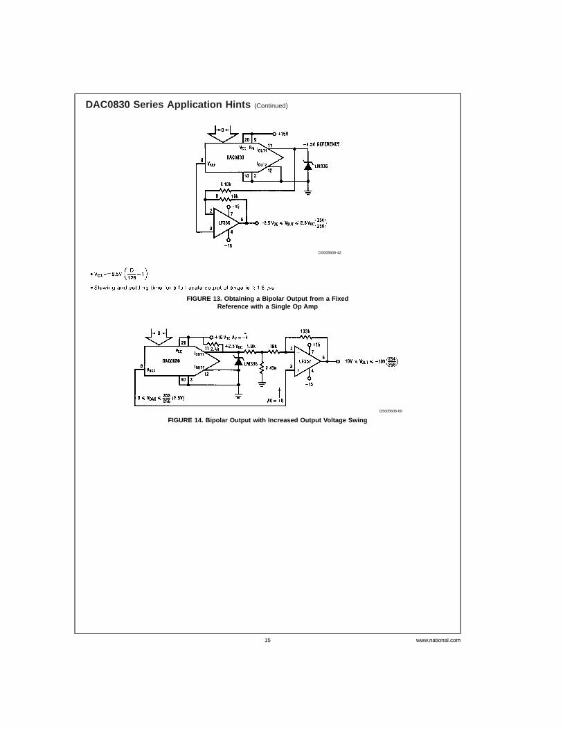
DAC0830 Series Application Hints (Continued)
DS005608-42
FIGURE 13. Obtaining a Bipolar Output from a FixedReference with a Single Op Amp
DS005608-60
FIGURE 14. Bipolar Output with Increased Output Voltage Swing
www.national.com15
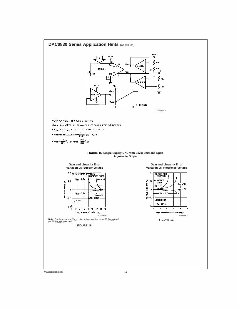
DAC0830 Series Application Hints (Continued)
DS005608-14
FIGURE 15. Single Supply DAC with Level Shift and Span-Adjustable Output
Gain and Linearity ErrorVariation vs. Supply Voltage
DS005608-32
Note: For these curves, VREF is the voltage applied to pin 11 (IOUT1) withpin 12 (IOUT2) grounded.
FIGURE 16.
Gain and Linearity ErrorVariation vs. Reference Voltage
DS005608-33
FIGURE 17.
www.national.com 16
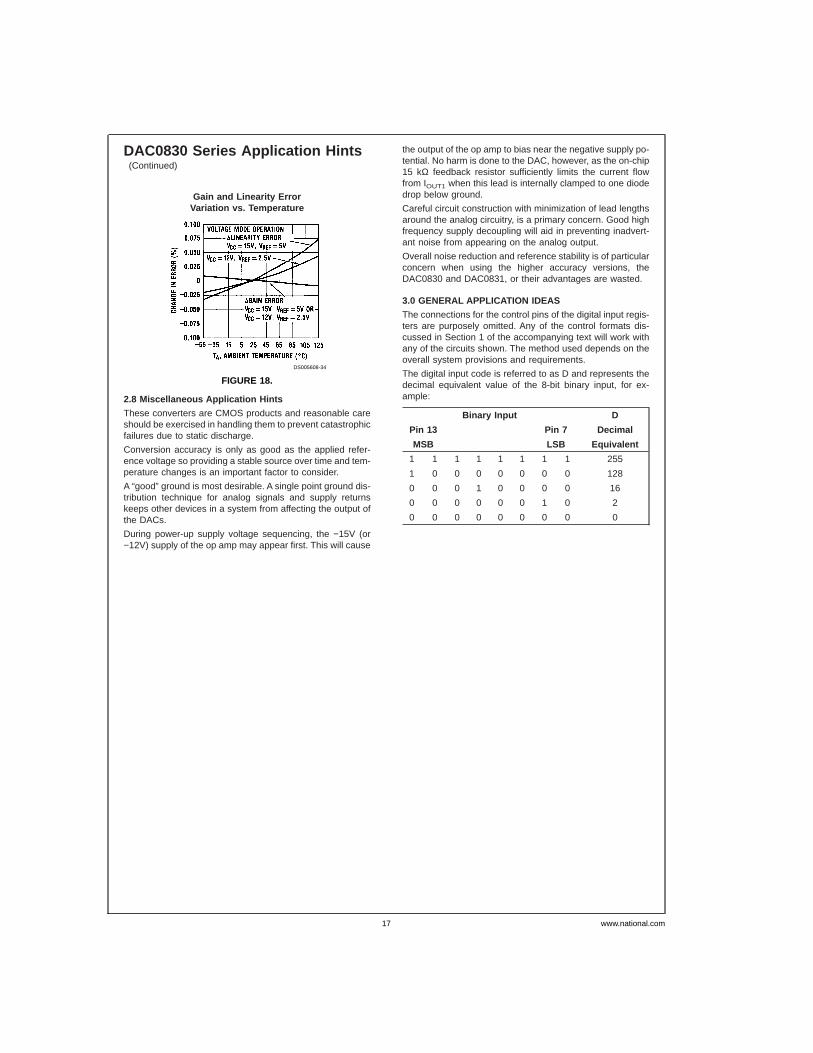
DAC0830 Series Application Hints(Continued)
2.8 Miscellaneous Application Hints
These converters are CMOS products and reasonable careshould be exercised in handling them to prevent catastrophicfailures due to static discharge.
Conversion accuracy is only as good as the applied refer-ence voltage so providing a stable source over time and tem-perature changes is an important factor to consider.
A “good” ground is most desirable. A single point ground dis-tribution technique for analog signals and supply returnskeeps other devices in a system from affecting the output ofthe DACs.
During power-up supply voltage sequencing, the −15V (or−12V) supply of the op amp may appear first. This will cause
the output of the op amp to bias near the negative supply po-tential. No harm is done to the DAC, however, as the on-chip15 kΩ feedback resistor sufficiently limits the current flowfrom IOUT1 when this lead is internally clamped to one diodedrop below ground.
Careful circuit construction with minimization of lead lengthsaround the analog circuitry, is a primary concern. Good highfrequency supply decoupling will aid in preventing inadvert-ant noise from appearing on the analog output.
Overall noise reduction and reference stability is of particularconcern when using the higher accuracy versions, theDAC0830 and DAC0831, or their advantages are wasted.
3.0 GENERAL APPLICATION IDEAS
The connections for the control pins of the digital input regis-ters are purposely omitted. Any of the control formats dis-cussed in Section 1 of the accompanying text will work withany of the circuits shown. The method used depends on theoverall system provisions and requirements.
The digital input code is referred to as D and represents thedecimal equivalent value of the 8-bit binary input, for ex-ample:
Binary Input D
Pin 13 Pin 7 Decimal
MSB LSB Equivalent
1 1 1 1 1 1 1 1 255
1 0 0 0 0 0 0 0 128
0 0 0 1 0 0 0 0 16
0 0 0 0 0 0 1 0 2
0 0 0 0 0 0 0 0 0
Gain and Linearity ErrorVariation vs. Temperature
DS005608-34
FIGURE 18.
www.national.com17
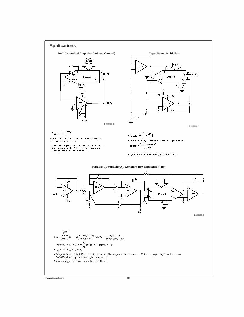
Applications
DAC Controlled Amplifier (Volume Control)
DS005608-43
Capacitance Multiplier
DS005608-44
Variable f O, Variable Q O, Constant BW Bandpass Filter
DS005608-17
www.national.com 18
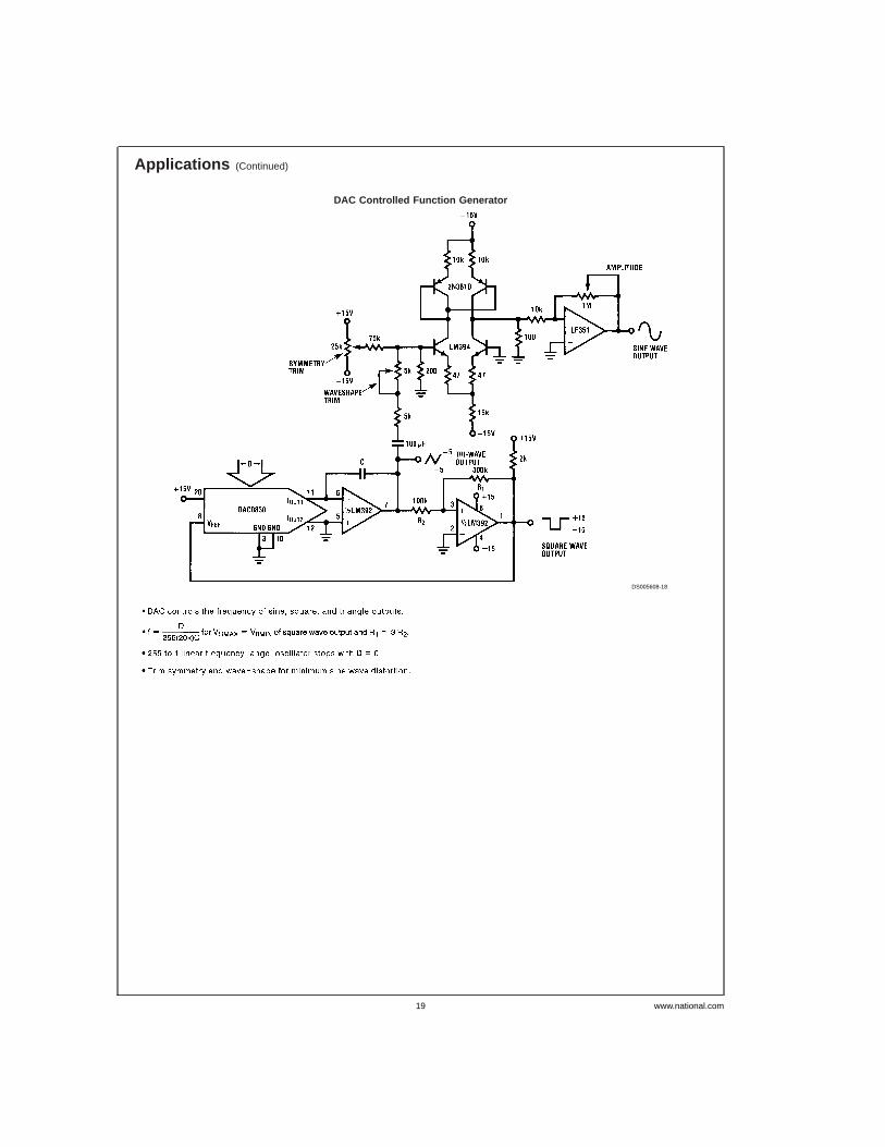
Applications (Continued)
DAC Controlled Function Generator
DS005608-18
www.national.com19
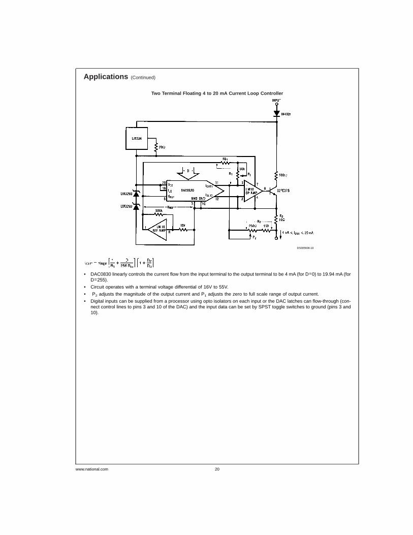
Applications (Continued)
Two Terminal Floating 4 to 20 mA Current Loop Controller
DS005608-19
• DAC0830 linearly controls the current flow from the input terminal to the output terminal to be 4 mA (for D=0) to 19.94 mA (forD=255).
• Circuit operates with a terminal voltage differential of 16V to 55V.
• P2 adjusts the magnitude of the output current and P1 adjusts the zero to full scale range of output current.
• Digital inputs can be supplied from a processor using opto isolators on each input or the DAC latches can flow-through (con-nect control lines to pins 3 and 10 of the DAC) and the input data can be set by SPST toggle switches to ground (pins 3 and10).
www.national.com 20
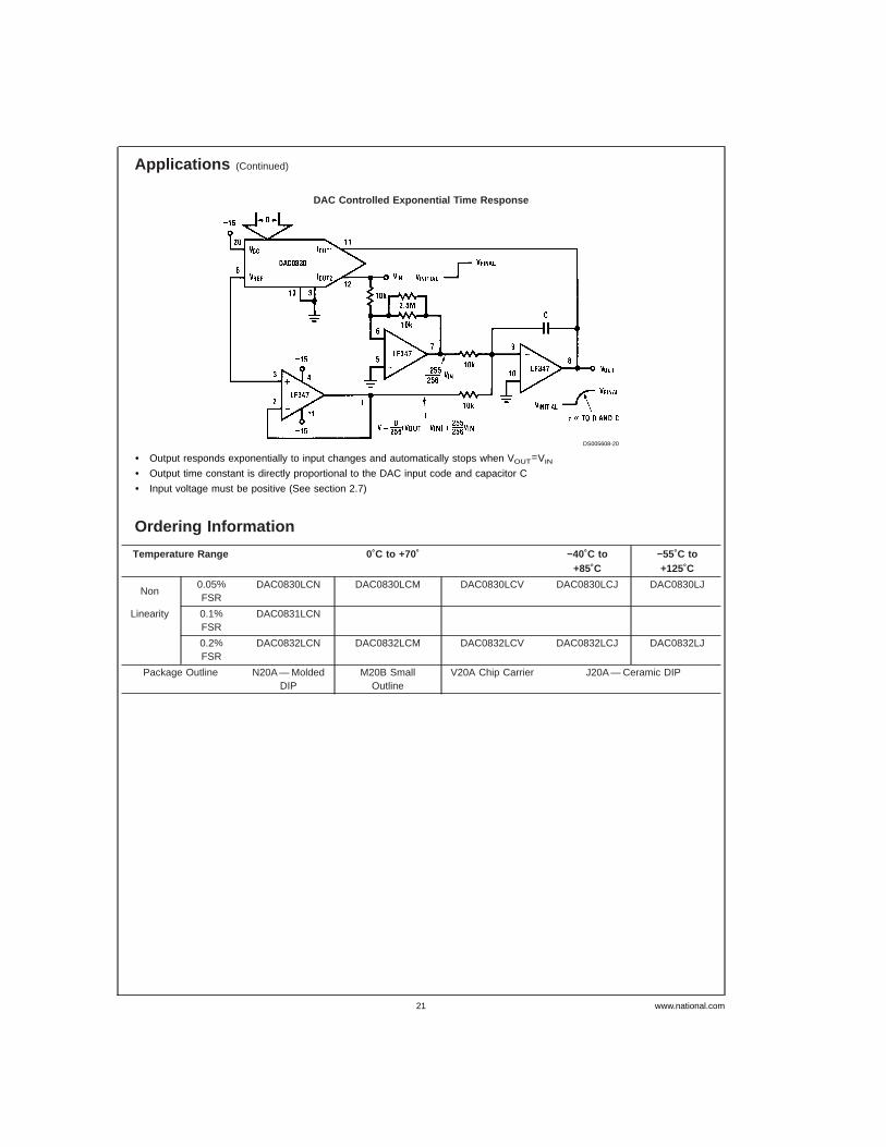
Applications (Continued)
Ordering Information
Temperature Range 0˚C to +70˚ −40˚C to+85˚C
−55˚C to+125˚C
Non0.05%FSR
DAC0830LCN DAC0830LCM DAC0830LCV DAC0830LCJ DAC0830LJ
Linearity 0.1%FSR
DAC0831LCN
0.2%FSR
DAC0832LCN DAC0832LCM DAC0832LCV DAC0832LCJ DAC0832LJ
Package Outline N20A — MoldedDIP
M20B SmallOutline
V20A Chip Carrier J20A — Ceramic DIP
DAC Controlled Exponential Time Response
DS005608-20
• Output responds exponentially to input changes and automatically stops when VOUT=VIN
• Output time constant is directly proportional to the DAC input code and capacitor C
• Input voltage must be positive (See section 2.7)
www.national.com21
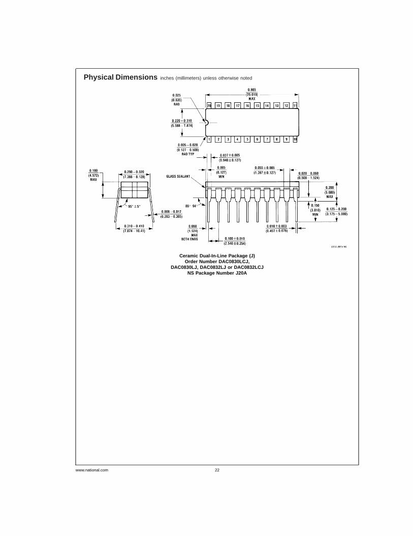
Physical Dimensions inches (millimeters) unless otherwise noted
Ceramic Dual-In-Line Package (J)Order Number DAC0830LCJ,
DAC0830LJ, DAC0832LJ or DAC0832LCJNS Package Number J20A
www.national.com 22
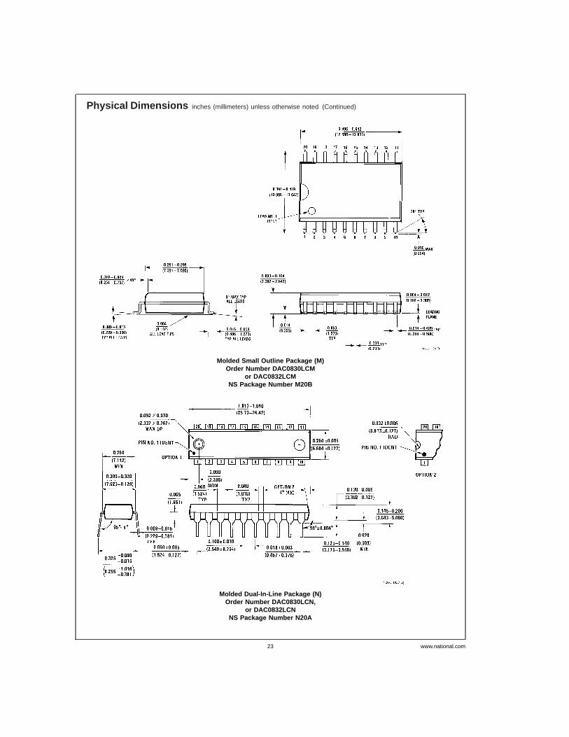
Physical Dimensions inches (millimeters) unless otherwise noted (Continued)
Molded Small Outline Package (M)Order Number DAC0830LCM
or DAC0832LCMNS Package Number M20B
Molded Dual-In-Line Package (N)Order Number DAC0830LCN,
or DAC0832LCNNS Package Number N20A
www.national.com23
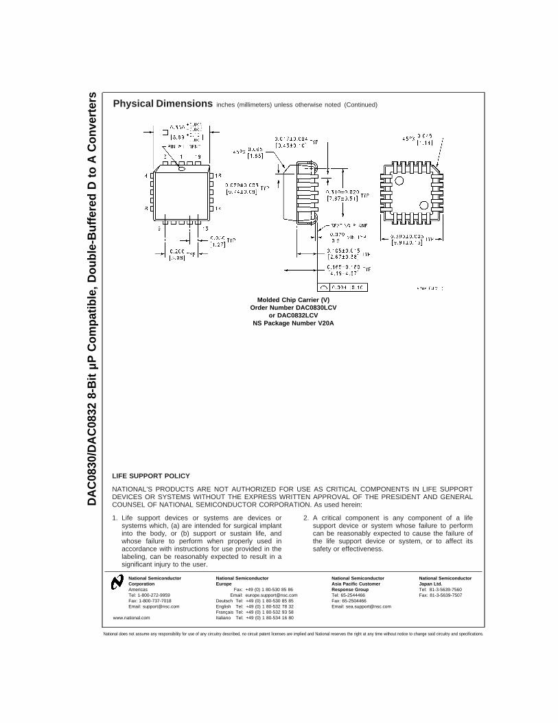
Physical Dimensions inches (millimeters) unless otherwise noted (Continued)
LIFE SUPPORT POLICY
NATIONAL’S PRODUCTS ARE NOT AUTHORIZED FOR USE AS CRITICAL COMPONENTS IN LIFE SUPPORTDEVICES OR SYSTEMS WITHOUT THE EXPRESS WRITTEN APPROVAL OF THE PRESIDENT AND GENERALCOUNSEL OF NATIONAL SEMICONDUCTOR CORPORATION. As used herein:
1. Life support devices or systems are devices orsystems which, (a) are intended for surgical implantinto the body, or (b) support or sustain life, andwhose failure to perform when properly used inaccordance with instructions for use provided in thelabeling, can be reasonably expected to result in asignificant injury to the user.
2. A critical component is any component of a lifesupport device or system whose failure to performcan be reasonably expected to cause the failure ofthe life support device or system, or to affect itssafety or effectiveness.
National SemiconductorCorporationAmericasTel: 1-800-272-9959Fax: 1-800-737-7018Email: [email protected]
National SemiconductorEurope
Fax: +49 (0) 1 80-530 85 86Email: [email protected]
Deutsch Tel: +49 (0) 1 80-530 85 85English Tel: +49 (0) 1 80-532 78 32Français Tel: +49 (0) 1 80-532 93 58Italiano Tel: +49 (0) 1 80-534 16 80
National SemiconductorAsia Pacific CustomerResponse GroupTel: 65-2544466Fax: 65-2504466Email: [email protected]
National SemiconductorJapan Ltd.Tel: 81-3-5639-7560Fax: 81-3-5639-7507
www.national.com
Molded Chip Carrier (V)Order Number DAC0830LCV
or DAC0832LCVNS Package Number V20A
DA
C08
30/D
AC
0832
8-B
itµP
Com
patib
le,D
oubl
e-B
uffe
red
Dto
AC
onve
rters
National does not assume any responsibility for use of any circuitry described, no circuit patent licenses are implied and National reserves the right at any time without notice to change said circuitry and specifications.
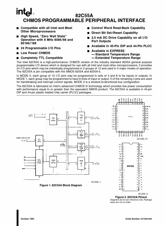
October 1995 Order Number: 231256-004
82C55ACHMOS PROGRAMMABLE PERIPHERAL INTERFACE
Y Compatible with all Intel and MostOther Microprocessors
Y High Speed, ‘‘Zero Wait State’’Operation with 8 MHz 8086/88 and80186/188
Y 24 Programmable I/O Pins
Y Low Power CHMOS
Y Completely TTL Compatible
Y Control Word Read-Back Capability
Y Direct Bit Set/Reset Capability
Y 2.5 mA DC Drive Capability on all I/OPort Outputs
Y Available in 40-Pin DIP and 44-Pin PLCC
Y Available in EXPRESSÐ Standard Temperature RangeÐ Extended Temperature Range
The Intel 82C55A is a high-performance, CHMOS version of the industry standard 8255A general purposeprogrammable I/O device which is designed for use with all Intel and most other microprocessors. It provides24 I/O pins which may be individually programmed in 2 groups of 12 and used in 3 major modes of operation.The 82C55A is pin compatible with the NMOS 8255A and 8255A-5.
In MODE 0, each group of 12 I/O pins may be programmed in sets of 4 and 8 to be inputs or outputs. InMODE 1, each group may be programmed to have 8 lines of input or output. 3 of the remaining 4 pins are usedfor handshaking and interrupt control signals. MODE 2 is a strobed bi-directional bus configuration.
The 82C55A is fabricated on Intel’s advanced CHMOS III technology which provides low power consumptionwith performance equal to or greater than the equivalent NMOS product. The 82C55A is available in 40-pinDIP and 44-pin plastic leaded chip carrier (PLCC) packages.
231256–1
Figure 1. 82C55A Block Diagram
231256–31
231256–2
Figure 2. 82C55A PinoutDiagrams are for pin reference only. Packagesizes are not to scale.
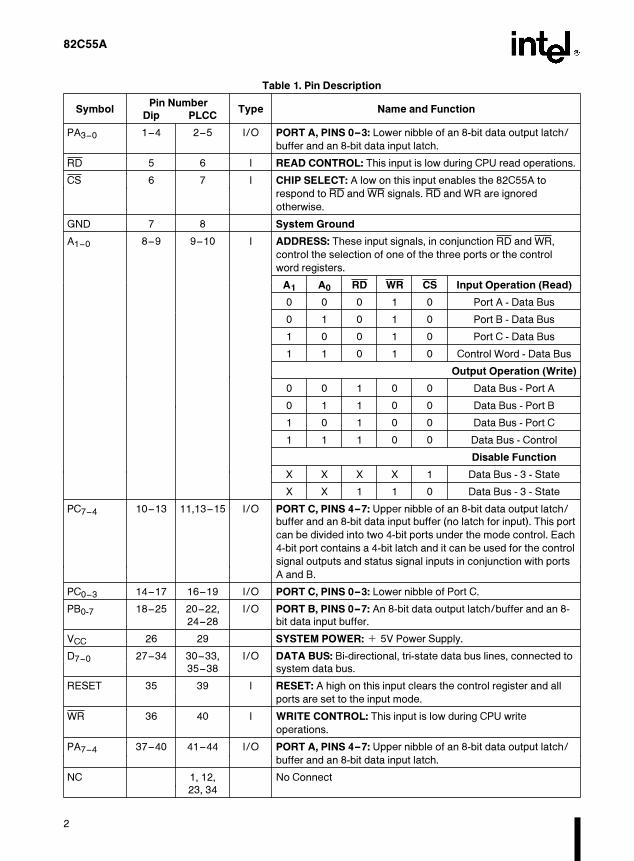
82C55A
Table 1. Pin Description
SymbolPin Number
Type Name and FunctionDip PLCC
PA3–0 1–4 2–5 I/O PORT A, PINS 0–3: Lower nibble of an 8-bit data output latch/
buffer and an 8-bit data input latch.
RD 5 6 I READ CONTROL: This input is low during CPU read operations.
CS 6 7 I CHIP SELECT: A low on this input enables the 82C55A to
respond to RD and WR signals. RD and WR are ignored
otherwise.
GND 7 8 System Ground
A1–0 8–9 9–10 I ADDRESS: These input signals, in conjunction RD and WR,
control the selection of one of the three ports or the control
word registers.
A1 A0 RD WR CS Input Operation (Read)
0 0 0 1 0 Port A - Data Bus
0 1 0 1 0 Port B - Data Bus
1 0 0 1 0 Port C - Data Bus
1 1 0 1 0 Control Word - Data Bus
Output Operation (Write)
0 0 1 0 0 Data Bus - Port A
0 1 1 0 0 Data Bus - Port B
1 0 1 0 0 Data Bus - Port C
1 1 1 0 0 Data Bus - Control
Disable Function
X X X X 1 Data Bus - 3 - State
X X 1 1 0 Data Bus - 3 - State
PC7–4 10–13 11,13–15 I/O PORT C, PINS 4–7: Upper nibble of an 8-bit data output latch/buffer and an 8-bit data input buffer (no latch for input). This port
can be divided into two 4-bit ports under the mode control. Each
4-bit port contains a 4-bit latch and it can be used for the control
signal outputs and status signal inputs in conjunction with ports
A and B.
PC0–3 14–17 16–19 I/O PORT C, PINS 0–3: Lower nibble of Port C.
PB0-7 18–25 20–22, I/O PORT B, PINS 0–7: An 8-bit data output latch/buffer and an 8-24–28 bit data input buffer.
VCC 26 29 SYSTEM POWER: a 5V Power Supply.
D7–0 27–34 30–33, I/O DATA BUS: Bi-directional, tri-state data bus lines, connected to35–38 system data bus.
RESET 35 39 I RESET: A high on this input clears the control register and all
ports are set to the input mode.
WR 36 40 I WRITE CONTROL: This input is low during CPU write
operations.
PA7–4 37–40 41–44 I/O PORT A, PINS 4–7: Upper nibble of an 8-bit data output latch/
buffer and an 8-bit data input latch.
NC 1, 12, No Connect23, 34
2
82C55A
82C55A FUNCTIONAL DESCRIPTION
General
The 82C55A is a programmable peripheral interfacedevice designed for use in Intel microcomputer sys-tems. Its function is that of a general purpose I/Ocomponent to interface peripheral equipment to themicrocomputer system bus. The functional configu-ration of the 82C55A is programmed by the systemsoftware so that normally no external logic is neces-sary to interface peripheral devices or structures.
Data Bus Buffer
This 3-state bidirectional 8-bit buffer is used to inter-face the 82C55A to the system data bus. Data istransmitted or received by the buffer upon executionof input or output instructions by the CPU. Controlwords and status information are also transferredthrough the data bus buffer.
Read/Write and Control Logic
The function of this block is to manage all of theinternal and external transfers of both Data andControl or Status words. It accepts inputs from theCPU Address and Control busses and in turn, issuescommands to both of the Control Groups.
Group A and Group B Controls
The functional configuration of each port is pro-grammed by the systems software. In essence, theCPU ‘‘outputs’’ a control word to the 82C55A. Thecontrol word contains information such as ‘‘mode’’,‘‘bit set’’, ‘‘bit reset’’, etc., that initializes the func-tional configuration of the 82C55A.
Each of the Control blocks (Group A and Group B)accepts ‘‘commands’’ from the Read/Write ControlLogic, receives ‘‘control words’’ from the internaldata bus and issues the proper commands to its as-sociated ports.
Control Group A - Port A and Port C upper (C7–C4)Control Group B - Port B and Port C lower (C3–C0)
The control word register can be both written andread as shown in the address decode table in thepin descriptions. Figure 6 shows the control wordformat for both Read and Write operations. Whenthe control word is read, bit D7 will always be a logic‘‘1’’, as this implies control word mode information.
Ports A, B, and C
The 82C55A contains three 8-bit ports (A, B, and C).All can be configured in a wide variety of functionalcharacteristics by the system software but each hasits own special features or ‘‘personality’’ to furtherenhance the power and flexibility of the 82C55A.
Port A. One 8-bit data output latch/buffer and one8-bit input latch buffer. Both ‘‘pull-up’’ and ‘‘pull-down’’ bus hold devices are present on Port A.
Port B. One 8-bit data input/output latch/buffer.Only ‘‘pull-up’’ bus hold devices are present on PortB.
Port C. One 8-bit data output latch/buffer and one8-bit data input buffer (no latch for input). This portcan be divided into two 4-bit ports under the modecontrol. Each 4-bit port contains a 4-bit latch and itcan be used for the control signal outputs and statussignal inputs in conjunction with ports A and B. Only‘‘pull-up’’ bus hold devices are present on Port C.
See Figure 4 for the bus-hold circuit configuration forPort A, B, and C.
3
82C55A
231256–3
Figure 3. 82C55A Block Diagram Showing Data Bus Buffer and Read/Write Control Logic Functions
*NOTE: 231256–4
Port pins loaded with more than 20 pF capacitance may not have their logic level guaranteed following a hardware reset.
Figure 4. Port A, B, C, Bus-hold Configuration
4
82C55A
82C55A OPERATIONAL DESCRIPTION
Mode Selection
There are three basic modes of operation that canbe selected by the system software:
Mode 0 Ð Basic input/outputMode 1 Ð Strobed Input/outputMode 2 Ð Bi-directional Bus
When the reset input goes ‘‘high’’ all ports will be setto the input mode with all 24 port lines held at a logic‘‘one’’ level by the internal bus hold devices (seeFigure 4 Note). After the reset is removed the82C55A can remain in the input mode with no addi-tional initialization required. This eliminates the needfor pullup or pulldown devices in ‘‘all CMOS’’ de-signs. During the execution of the system program,any of the other modes may be selected by using asingle output instruction. This allows a single82C55A to service a variety of peripheral deviceswith a simple software maintenance routine.
The modes for Port A and Port B can be separatelydefined, while Port C is divided into two portions asrequired by the Port A and Port B definitions. All ofthe output registers, including the status flip-flops,will be reset whenever the mode is changed. Modesmay be combined so that their functional definitioncan be ‘‘tailored’’ to almost any I/O structure. Forinstance; Group B can be programmed in Mode 0 tomonitor simple switch closings or display computa-tional results, Group A could be programmed inMode 1 to monitor a keyboard or tape reader on aninterrupt-driven basis.
231256–5
Figure 5. Basic Mode Definitions and Bus
Interface
231256–6
Figure 6. Mode Definition Format
The mode definitions and possible mode combina-tions may seem confusing at first but after a cursoryreview of the complete device operation a simple,logical I/O approach will surface. The design of the82C55A has taken into account things such as effi-cient PC board layout, control signal definition vs PClayout and complete functional flexibility to supportalmost any peripheral device with no external logic.Such design represents the maximum use of theavailable pins.
Single Bit Set/Reset Feature
Any of the eight bits of Port C can be Set or Resetusing a single OUTput instruction. This feature re-duces software requirements in Control-based appli-cations.
When Port C is being used as status/control for PortA or B, these bits can be set or reset by using the BitSet/Reset operation just as if they were data outputports.
5
82C55A
231256–7
Figure 7. Bit Set/Reset Format
Interrupt Control Functions
When the 82C55A is programmed to operate inmode 1 or mode 2, control signals are provided thatcan be used as interrupt request inputs to the CPU.The interrupt request signals, generated from port C,can be inhibited or enabled by setting or resettingthe associated INTE flip-flop, using the bit set/resetfunction of port C.
This function allows the Programmer to disallow orallow a specific I/O device to interrupt the CPU with-out affecting any other device in the interrupt struc-ture.
INTE flip-flop definition:
(BIT-SET)ÐINTE is SETÐInterrupt enable(BIT-RESET)ÐINTE is RESETÐInterrupt disable
Note:All Mask flip-flops are automatically reset duringmode selection and device Reset.
6
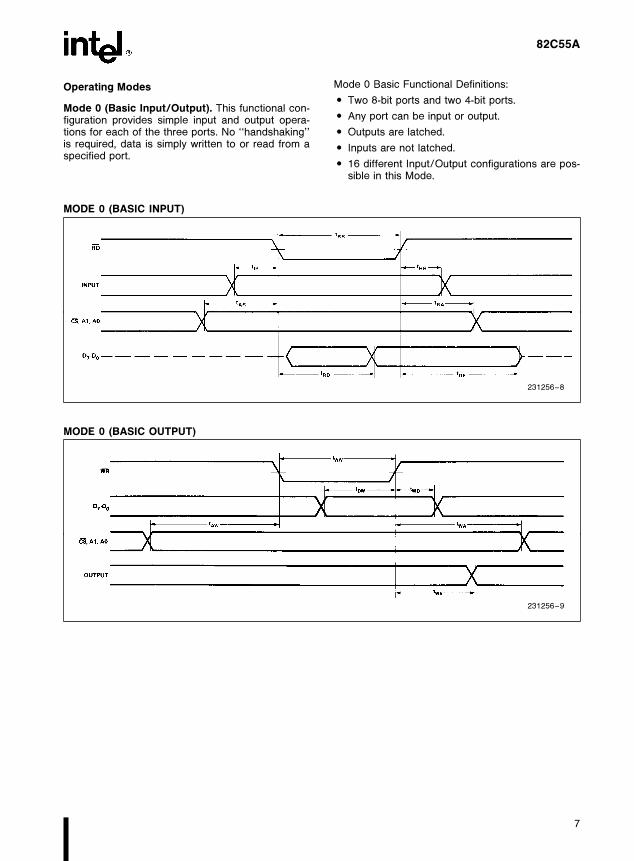
82C55A
Operating Modes
Mode 0 (Basic Input/Output). This functional con-figuration provides simple input and output opera-tions for each of the three ports. No ‘‘handshaking’’is required, data is simply written to or read from aspecified port.
Mode 0 Basic Functional Definitions:
# Two 8-bit ports and two 4-bit ports.
# Any port can be input or output.
# Outputs are latched.
# Inputs are not latched.
# 16 different Input/Output configurations are pos-sible in this Mode.
MODE 0 (BASIC INPUT)
231256–8
MODE 0 (BASIC OUTPUT)
231256–9
7
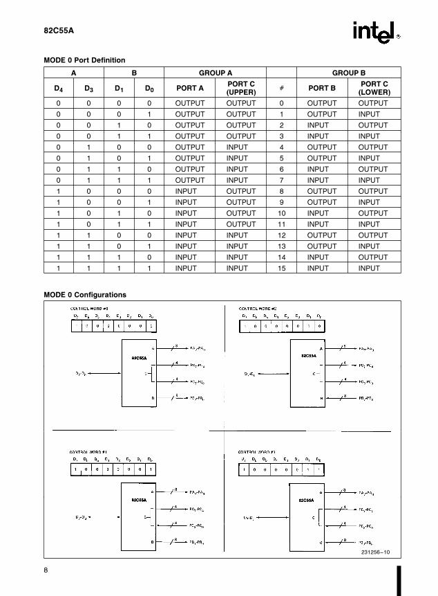
82C55A
MODE 0 Port Definition
A B GROUP A GROUP B
D4 D3 D1 D0 PORT APORT C Ý PORT B
PORT C(UPPER) (LOWER)
0 0 0 0 OUTPUT OUTPUT 0 OUTPUT OUTPUT
0 0 0 1 OUTPUT OUTPUT 1 OUTPUT INPUT
0 0 1 0 OUTPUT OUTPUT 2 INPUT OUTPUT
0 0 1 1 OUTPUT OUTPUT 3 INPUT INPUT
0 1 0 0 OUTPUT INPUT 4 OUTPUT OUTPUT
0 1 0 1 OUTPUT INPUT 5 OUTPUT INPUT
0 1 1 0 OUTPUT INPUT 6 INPUT OUTPUT
0 1 1 1 OUTPUT INPUT 7 INPUT INPUT
1 0 0 0 INPUT OUTPUT 8 OUTPUT OUTPUT
1 0 0 1 INPUT OUTPUT 9 OUTPUT INPUT
1 0 1 0 INPUT OUTPUT 10 INPUT OUTPUT
1 0 1 1 INPUT OUTPUT 11 INPUT INPUT
1 1 0 0 INPUT INPUT 12 OUTPUT OUTPUT
1 1 0 1 INPUT INPUT 13 OUTPUT INPUT
1 1 1 0 INPUT INPUT 14 INPUT OUTPUT
1 1 1 1 INPUT INPUT 15 INPUT INPUT
MODE 0 Configurations
231256–10
8
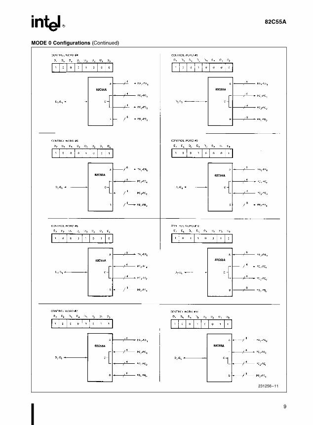
82C55A
MODE 0 Configurations (Continued)
231256–11
9
82C55A
MODE 0 Configurations (Continued)
231256–12
Operating Modes
MODE 1 (Strobed Input/Output). This functionalconfiguration provides a means for transferring I/Odata to or from a specified port in conjunction withstrobes or ‘‘handshaking’’ signals. In mode 1, Port Aand Port B use the lines on Port C to generate oraccept these ‘‘handshaking’’ signals.
Mode 1 Basic functional Definitions:
# Two Groups (Group A and Group B).
# Each group contains one 8-bit data port and one4-bit control/data port.
# The 8-bit data port can be either input or outputBoth inputs and outputs are latched.
# The 4-bit port is used for control and status of the8-bit data port.
10
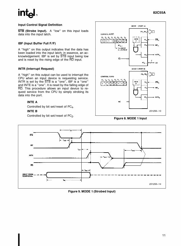
82C55A
Input Control Signal Definition
STB (Strobe Input). A ‘‘low’’ on this input loadsdata into the input latch.
IBF (Input Buffer Full F/F)
A ‘‘high’’ on this output indicates that the data hasbeen loaded into the input latch; in essence, an ac-knowledgement. IBF is set by STB input being lowand is reset by the rising edge of the RD input.
INTR (Interrupt Request)
A ‘‘high’’ on this output can be used to interrupt theCPU when an input device is requesting service.INTR is set by the STB is a ‘‘one’’, IBF is a ‘‘one’’and INTE is a ‘‘one’’. It is reset by the falling edge ofRD. This procedure allows an input device to re-quest service from the CPU by simply strobing itsdata into the port.
INTE A
Controlled by bit set/reset of PC4.
INTE B
Controlled by bit set/reset of PC2.
231256–13
Figure 8. MODE 1 Input
231256–14
Figure 9. MODE 1 (Strobed Input)
11
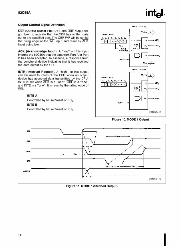
82C55A
Output Control Signal Definition
OBF (Output Buffer Full F/F). The OBF output willgo ‘‘low’’ to indicate that the CPU has written dataout to the specified port. The OBF F/F will be set bythe rising edge of the WR input and reset by ACKInput being low.
ACK (Acknowledge Input). A ‘‘low’’ on this inputinforms the 82C55A that the data from Port A or PortB has been accepted. In essence, a response fromthe peripheral device indicating that it has receivedthe data output by the CPU.
INTR (Interrupt Request). A ‘‘high’’ on this outputcan be used to interrupt the CPU when an outputdevice has accepted data transmitted by the CPU.INTR is set when ACK is a ‘‘one’’, OBF is a ‘‘one’’and INTE is a ‘‘one’’. It is reset by the falling edge ofWR.
INTE A
Controlled by bit set/reset of PC6.
INTE B
Controlled by bit set/reset of PC2.231256–15
Figure 10. MODE 1 Output
231256–16
Figure 11. MODE 1 (Strobed Output)
12
82C55A
Combinations of MODE 1
Port A and Port B can be individually defined as input or output in Mode 1 to support a wide variety of strobedI/O applications.
231256–17
Figure 12. Combinations of MODE 1
Operating Modes
MODE 2 (Strobed Bidirectional Bus I/O).Thisfunctional configuration provides a means for com-municating with a peripheral device or structure on asingle 8-bit bus for both transmitting and receivingdata (bidirectional bus I/O). ‘‘Handshaking’’ signalsare provided to maintain proper bus flow discipline ina similar manner to MODE 1. Interrupt generationand enable/disable functions are also available.
MODE 2 Basic Functional Definitions:
# Used in Group A only.
# One 8-bit, bi-directional bus port (Port A) and a 5-bit control port (Port C).
# Both inputs and outputs are latched.
# The 5-bit control port (Port C) is used for controland status for the 8-bit, bi-directional bus port(Port A).
Bidirectional Bus I/O Control Signal Definition
INTR (Interrupt Request). A high on this output canbe used to interrupt the CPU for input or output oper-ations.
Output Operations
OBF (Output Buffer Full). The OBF output will go‘‘low’’ to indicate that the CPU has written data outto port A.
ACK (Acknowledge). A ‘‘low’’ on this input enablesthe tri-state output buffer of Port A to send out thedata. Otherwise, the output buffer will be in the highimpedance state.
INTE 1 (The INTE Flip-Flop Associated withOBF). Controlled by bit set/reset of PC6.
Input Operations
STB (Strobe Input). A ‘‘low’’ on this input loadsdata into the input latch.
IBF (Input Buffer Full F/F). A ‘‘high’’ on this outputindicates that data has been loaded into the inputlatch.
INTE 2 (The INTE Flip-Flop Associated with IBF).Controlled by bit set/reset of PC4.
13
82C55A
231256–18
Figure 13. MODE Control Word231256–19
Figure 14. MODE 2
231256–20
Figure 15. MODE 2 (Bidirectional)
NOTE:Any sequence where WR occurs before ACK, and STB occurs before RD is permissible.(INTR e IBF # MASK # STB # RD a OBF # MASK # ACK # WR)
14
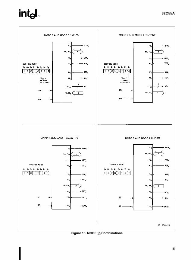
82C55A
231256–21
Figure 16. MODE (/4 Combinations
15
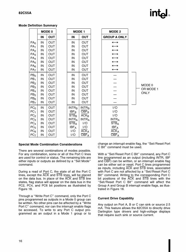
82C55A
Mode Definition Summary
MODE 0 MODE 1 MODE 2
IN OUT IN OUT GROUP A ONLY
PA0 IN OUT IN OUT ÝPA1 IN OUT IN OUT ÝPA2 IN OUT IN OUT ÝPA3 IN OUT IN OUT ÝPA4 IN OUT IN OUT ÝPA5 IN OUT IN OUT ÝPA6 IN OUT IN OUT ÝPA7 IN OUT IN OUT ÝPB0 IN OUT IN OUT Ð
PB1 IN OUT IN OUT Ð
PB2 IN OUT IN OUT Ð
PB3 IN OUT IN OUT ÐMODE 0
PB4 IN OUT IN OUT ÐOR MODE 1
PB5 IN OUT IN OUT ÐONLY
PB6 IN OUT IN OUT Ð
PB7 IN OUT IN OUT Ð
PC0 IN OUT INTRB INTRB I/O
PC1 IN OUT IBFB OBFB I/O
PC2 IN OUT STBB ACKB I/O
PC3 IN OUT INTRA INTRA INTRA
PC4 IN OUT STBA I/O STBA
PC5 IN OUT IBFA I/O IBFA
PC6 IN OUT I/O ACKA ACKA
PC7 IN OUT I/O OBFA OBFA
Special Mode Combination Considerations
There are several combinations of modes possible.For any combination, some or all of the Port C linesare used for control or status. The remaining bits areeither inputs or outputs as defined by a ‘‘Set Mode’’command.
During a read of Port C, the state of all the Port Clines, except the ACK and STB lines, will be placedon the data bus. In place of the ACK and STB linestates, flag status will appear on the data bus in thePC2, PC4, and PC6 bit positions as illustrated byFigure 18.
Through a ‘‘Write Port C’’ command, only the Port Cpins programmed as outputs in a Mode 0 group canbe written. No other pins can be affected by a ‘‘WritePort C’’ command, nor can the interrupt enable flagsbe accessed. To write to any Port C output pro-grammed as an output in a Mode 1 group or to
change an interrupt enable flag, the ‘‘Set/Reset PortC Bit’’ command must be used.
With a ‘‘Set/Reset Port C Bit’’ command, any Port Cline programmed as an output (including INTR, IBFand OBF) can be written, or an interrupt enable flagcan be either set or reset. Port C lines programmedas inputs, including ACK and STB lines, associatedwith Port C are not affected by a ‘‘Set/Reset Port CBit’’ command. Writing to the corresponding Port Cbit positions of the ACK and STB lines with the‘‘Set/Reset Port C Bit’’ command will affect theGroup A and Group B interrupt enable flags, as illus-trated in Figure 18.
Current Drive Capability
Any output on Port A, B or C can sink or source 2.5mA. This feature allows the 82C55A to directly driveDarlington type drivers and high-voltage displaysthat require such sink or source current.
16

82C55A
Reading Port C Status
In Mode 0, Port C transfers data to or from the pe-ripheral device. When the 82C55A is programmed tofunction in Modes 1 or 2, Port C generates or ac-cepts ‘‘hand-shaking’’ signals with the peripheral de-vice. Reading the contents of Port C allows the pro-grammer to test or verify the ‘‘status’’ of each pe-ripheral device and change the program flow ac-cordingly.
There is no special instruction to read the status in-formation from Port C. A normal read operation ofPort C is executed to perform this function.
INPUT CONFIGURATION
D7 D6 D5 D4 D3 D2 D1 D0
I/O I/O IBFA INTEA INTRA INTEB IBFB INTRB
GROUP A GROUP B
OUTPUT CONFIGURATIONS
D7 D6 D5 D4 D3 D2 D1 D0
OBFA INTEA I/O I/O INTRA INTEB OBFB INTRB
GROUP A GROUP B
Figure 17a. MODE 1 Status Word Format
D7 D6 D5 D4 D3 D2 D1 D0
OBFA INTE1 IBFA INTE2 INTRA
GROUP A GROUP B
(Defined By Mode 0 or Mode 1 Selection)
Figure 17b. MODE 2 Status Word Format
Interrupt Enable Flag Position Alternate Port C Pin Signal (Mode)
INTE B PC2 ACKB (Output Mode 1) or STBB (Input Mode 1)
INTE A2 PC4 STBA (Input Mode 1 or Mode 2)
INTE A1 PC6 ACKA (Output Mode 1 or Mode 2
Figure 18. Interrupt Enable Flags in Modes 1 and 2
17
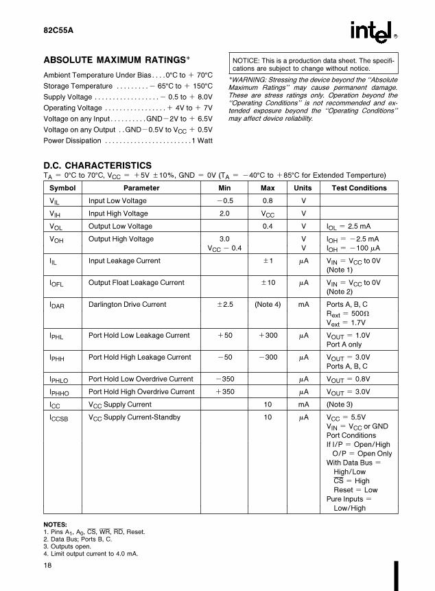
82C55A
ABSOLUTE MAXIMUM RATINGS*
Ambient Temperature Under BiasÀÀÀÀ0§C to a 70§CStorage Temperature ÀÀÀÀÀÀÀÀÀb 65§C to a 150§CSupply Voltage ÀÀÀÀÀÀÀÀÀÀÀÀÀÀÀÀÀÀb 0.5 to a 8.0V
Operating Voltage ÀÀÀÀÀÀÀÀÀÀÀÀÀÀÀÀÀa 4V to a 7V
Voltage on any InputÀÀÀÀÀÀÀÀÀÀGNDb2V to a 6.5V
Voltage on any Output ÀÀGNDb0.5V to VCC a 0.5V
Power Dissipation ÀÀÀÀÀÀÀÀÀÀÀÀÀÀÀÀÀÀÀÀÀÀÀÀ1 Watt
NOTICE: This is a production data sheet. The specifi-cations are subject to change without notice.
*WARNING: Stressing the device beyond the ‘‘AbsoluteMaximum Ratings’’ may cause permanent damage.These are stress ratings only. Operation beyond the‘‘Operating Conditions’’ is not recommended and ex-tended exposure beyond the ‘‘Operating Conditions’’may affect device reliability.
D.C. CHARACTERISTICSTA e 0§C to 70§C, VCC e a5V g10%, GND e 0V (TA e b40§C to a85§C for Extended Temperture)
Symbol Parameter Min Max Units Test Conditions
VIL Input Low Voltage b0.5 0.8 V
VIH Input High Voltage 2.0 VCC V
VOL Output Low Voltage 0.4 V IOL e 2.5 mA
VOH Output High Voltage 3.0 V IOH e b2.5 mA
VCC b 0.4 V IOH e b100 mA
IIL Input Leakage Current g1 mA VIN e VCC to 0V
(Note 1)
IOFL Output Float Leakage Current g10 mA VIN e VCC to 0V
(Note 2)
IDAR Darlington Drive Current g2.5 (Note 4) mA Ports A, B, C
Rext e 500XVext e 1.7V
IPHL Port Hold Low Leakage Current a50 a300 mA VOUT e 1.0V
Port A only
IPHH Port Hold High Leakage Current b50 b300 mA VOUT e 3.0V
Ports A, B, C
IPHLO Port Hold Low Overdrive Current b350 mA VOUT e 0.8V
IPHHO Port Hold High Overdrive Current a350 mA VOUT e 3.0V
ICC VCC Supply Current 10 mA (Note 3)
ICCSB VCC Supply Current-Standby 10 mA VCC e 5.5V
VIN e VCC or GND
Port Conditions
If I/P e Open/High
O/P e Open Only
With Data Bus e
High/Low
CS e High
Reset e Low
Pure Inputs e
Low/High
NOTES:1. Pins A1, A0, CS, WR, RD, Reset.2. Data Bus; Ports B, C.3. Outputs open.4. Limit output current to 4.0 mA.
18
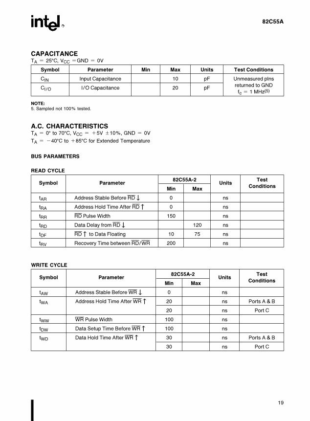
82C55A
CAPACITANCETA e 25§C, VCC eGND e 0V
Symbol Parameter Min Max Units Test Conditions
CIN Input Capacitance 10 pF Unmeasured plns
returned to GNDCI/O I/O Capacitance 20 pF
fc e 1 MHz(5)
NOTE:5. Sampled not 100% tested.
A.C. CHARACTERISTICSTA e 0§ to 70§C, VCC e a5V g10%, GND e 0V
TA e b40§C to a85§C for Extended Temperature
BUS PARAMETERS
READ CYCLE
Symbol Parameter82C55A-2
UnitsTest
Min MaxConditions
tAR Address Stable Before RDv 0 ns
tRA Address Hold Time After RDu 0 ns
tRR RD Pulse Width 150 ns
tRD Data Delay from RDv 120 ns
tDF RDu to Data Floating 10 75 ns
tRV Recovery Time between RD/WR 200 ns
WRITE CYCLE
Symbol Parameter82C55A-2
UnitsTest
Min MaxConditions
tAW Address Stable Before WRv 0 ns
tWA Address Hold Time After WRu 20 ns Ports A & B
20 ns Port C
tWW WR Pulse Width 100 ns
tDW Data Setup Time Before WRu 100 ns
tWD Data Hold Time After WRu 30 ns Ports A & B
30 ns Port C
19
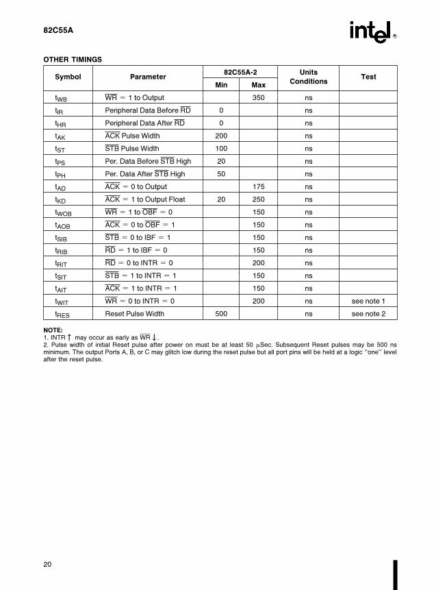
82C55A
OTHER TIMINGS
Symbol Parameter82C55A-2 Units
TestMin Max
Conditions
tWB WR e 1 to Output 350 ns
tlR Peripheral Data Before RD 0 ns
tHR Peripheral Data After RD 0 ns
tAK ACK Pulse Width 200 ns
tST STB Pulse Width 100 ns
tPS Per. Data Before STB High 20 ns
tPH Per. Data After STB High 50 ns
tAD ACK e 0 to Output 175 ns
tKD ACK e 1 to Output Float 20 250 ns
tWOB WR e 1 to OBF e 0 150 ns
tAOB ACK e 0 to OBF e 1 150 ns
tSIB STB e 0 to IBF e 1 150 ns
tRIB RD e 1 to IBF e 0 150 ns
tRIT RD e 0 to INTR e 0 200 ns
tSIT STB e 1 to INTR e 1 150 ns
tAIT ACK e 1 to INTR e 1 150 ns
tWIT WR e 0 to INTR e 0 200 ns see note 1
tRES Reset Pulse Width 500 ns see note 2
NOTE:1. INTRu may occur as early as WRv.2. Pulse width of initial Reset pulse after power on must be at least 50 mSec. Subsequent Reset pulses may be 500 nsminimum. The output Ports A, B, or C may glitch low during the reset pulse but all port pins will be held at a logic ‘‘one’’ levelafter the reset pulse.
20
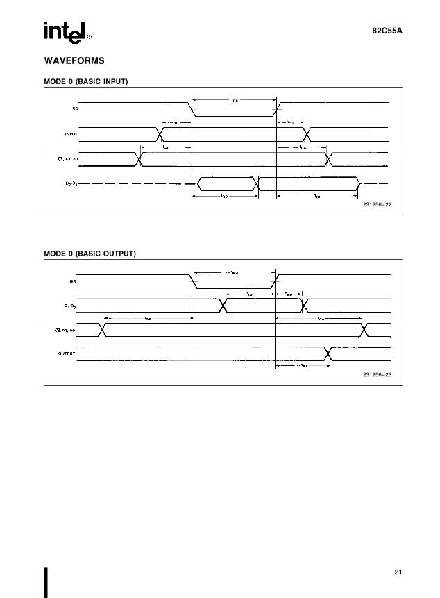
82C55A
WAVEFORMS
MODE 0 (BASIC INPUT)
231256–22
MODE 0 (BASIC OUTPUT)
231256–23
21
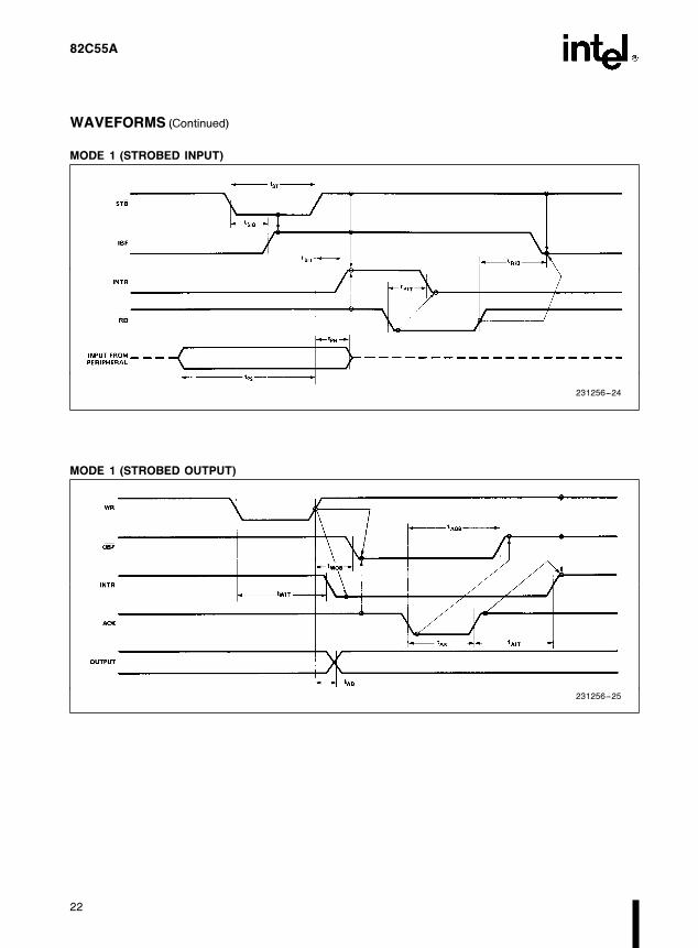
82C55A
WAVEFORMS (Continued)
MODE 1 (STROBED INPUT)
231256–24
MODE 1 (STROBED OUTPUT)
231256–25
22
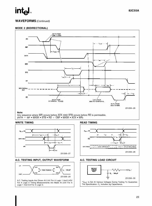
82C55A
WAVEFORMS (Continued)
MODE 2 (BIDIRECTIONAL)
231256–26
Note:Any sequence where WR occurs before ACK AND STB occurs before RD is permissible.(INTR e IBF # MASK # STB # RD a OBF # MASK # ACK # WR)
WRITE TIMING
231256–27
READ TIMING
231256–28
A.C. TESTING INPUT, OUTPUT WAVEFORM
231256–29
A.C. Testing Inputs Are Driven At 2.4V For A Logic 1 And 0.45VFor A Logic 0 Timing Measurements Are Made At 2.0V For ALogic 1 And 0.8 For A Logic 0.
A.C. TESTING LOAD CIRCUIT
231256–30
*VEXT Is Set At Various Voltages During Testing To GuaranteeThe Specification. CL Includes Jig Capacitance.
23
Related Documents


