HDMI Connector HOTPLUG UTILITY TMDS D2+ CEC DDC_CLK DDC_DAT TMDS D0– TMDS CLK+ TMDS D1+ TMDS D1– TMDS D0+ TMDS CLK– TMDS D2– P 5V0 GND To System TMDS GND TMDS GND ESD204 ESD204 TPD4E05U06 Product Folder Order Now Technical Documents Tools & Software Support & Community An IMPORTANT NOTICE at the end of this data sheet addresses availability, warranty, changes, use in safety-critical applications, intellectual property matters and other important disclaimers. PRODUCTION DATA. ESD204 SLVSEE2A – FEBRUARY 2018 – REVISED APRIL 2018 ESD204 4-Channel Low-Capacitance Surge and ESD Protection Diode 1 1 Features 1• IEC 61000-4-2 Level 4 ESD Protection – ±30-kV Contact Discharge – ±30-kV Air Gap Discharge • IEC 61000-4-4 EFT Protection – 80 A (5/50 ns) • IEC 61000-4-5 Surge Protection – 5.5 A (8/20 μs) – Low Surge Clamping Voltage 8.5 V at 5.5 A I PP • IO Capacitance: – 0.55 pF (Typical) • HDMI 2.0 Compliant • DC Breakdown Voltage: 5.5 V (Minimum) • Ultra Low Leakage Current: 10 nA (Maximum) • Supports High Speed Interfaces up to 6 Gbps • Industrial Temperature Range: –40°C to +125°C • Easy Flow-Through Routing Package 2 Applications • End Equipment – IP Network Camera – DVR and NVR – Ethernet Switches and Routers – Laptops and Desktops – Set-Top Boxes – TV and Monitors – Mobile and Tablets • Interfaces – HDMI 2.0 – HDMI 1.4 – USB 3.0 – Display Port 1.3 – PCI Express 3.0 – Ethernet 10/100/1000 Mbps 3 Description The ESD204 is a bidirectional TVS ESD protection diode array for HDMI and USB surge protection up to 5.5 A (8/20 μs). The ESD204 is rated to dissipate ESD strikes at the maximum level specified in the IEC 61000-4-2 international standard (Level 4). The low clamping and high differential bandwidth provided by ESD204 enables the device to cleanly pass high speed signals while providing robust protection to downstream devices. This device has a low capacitance of 0.55-pF per channel making it suitable for protecting high-speed interfaces up to 6 Gbps such as HDMI 2.0, HDMI 1.4, USB 3.0 and Ethernet 1G. The low dynamic resistance and low clamping voltage ensure system level protection against transient events. The ESD204 is offered in the industry standard USON-10 (DQA) package. The package features flow-through routing and 0.5-mm pin pitch easing implementation and reducing design time. Device Information (1) PART NUMBER PACKAGE BODY SIZE (NOM) ESD204 USON (10) 2.50 mm × 1.00 mm (1) For all available packages, see the orderable addendum at the end of the data sheet. Typical Application Schematic

Welcome message from author
This document is posted to help you gain knowledge. Please leave a comment to let me know what you think about it! Share it to your friends and learn new things together.
Transcript
HD
MI C
onnector
HOTPLUG
UTILITY
TMDS D2+
CEC
DDC_CLK
DDC_DAT
TMDS D0±
TMDS CLK+
TMDS D1+
TMDS D1±
TMDS D0+
TMDS CLK±
TMDS D2±
P 5V0
GND
To System
TMDS GND
TMDS GND
ESD204
ESD204
TPD4E05U06
Product
Folder
Order
Now
Technical
Documents
Tools &
Software
Support &Community
An IMPORTANT NOTICE at the end of this data sheet addresses availability, warranty, changes, use in safety-critical applications,intellectual property matters and other important disclaimers. PRODUCTION DATA.
ESD204SLVSEE2A –FEBRUARY 2018–REVISED APRIL 2018
ESD204 4-Channel Low-Capacitance Surge and ESD Protection Diode
1
1 Features1• IEC 61000-4-2 Level 4 ESD Protection
– ±30-kV Contact Discharge– ±30-kV Air Gap Discharge
• IEC 61000-4-4 EFT Protection– 80 A (5/50 ns)
• IEC 61000-4-5 Surge Protection– 5.5 A (8/20 μs)– Low Surge Clamping Voltage
8.5 V at 5.5 A IPP
• IO Capacitance:– 0.55 pF (Typical)
• HDMI 2.0 Compliant• DC Breakdown Voltage: 5.5 V (Minimum)• Ultra Low Leakage Current: 10 nA (Maximum)• Supports High Speed Interfaces up to 6 Gbps• Industrial Temperature Range: –40°C to +125°C• Easy Flow-Through Routing Package
2 Applications• End Equipment
– IP Network Camera– DVR and NVR– Ethernet Switches and Routers– Laptops and Desktops– Set-Top Boxes– TV and Monitors– Mobile and Tablets
• Interfaces– HDMI 2.0– HDMI 1.4– USB 3.0– Display Port 1.3– PCI Express 3.0– Ethernet 10/100/1000 Mbps
3 DescriptionThe ESD204 is a bidirectional TVS ESD protectiondiode array for HDMI and USB surge protection up to5.5 A (8/20 μs). The ESD204 is rated to dissipateESD strikes at the maximum level specified in theIEC 61000-4-2 international standard (Level 4).
The low clamping and high differential bandwidthprovided by ESD204 enables the device to cleanlypass high speed signals while providing robustprotection to downstream devices. This device has alow capacitance of 0.55-pF per channel making itsuitable for protecting high-speed interfaces up to 6Gbps such as HDMI 2.0, HDMI 1.4, USB 3.0 andEthernet 1G. The low dynamic resistance and lowclamping voltage ensure system level protectionagainst transient events.
The ESD204 is offered in the industry standardUSON-10 (DQA) package. The package featuresflow-through routing and 0.5-mm pin pitch easingimplementation and reducing design time.
Device Information(1)
PART NUMBER PACKAGE BODY SIZE (NOM)ESD204 USON (10) 2.50 mm × 1.00 mm
(1) For all available packages, see the orderable addendum atthe end of the data sheet.
Typical Application Schematic

2
ESD204SLVSEE2A –FEBRUARY 2018–REVISED APRIL 2018 www.ti.com
Product Folder Links: ESD204
Submit Documentation Feedback Copyright © 2018, Texas Instruments Incorporated
Table of Contents1 Features .................................................................. 12 Applications ........................................................... 13 Description ............................................................. 14 Revision History..................................................... 25 Pin Configuration and Functions ......................... 36 Specifications......................................................... 4
6.1 Absolute Maximum Ratings ...................................... 46.2 ESD Ratings -JEDEC Specifications ........................ 46.3 ESD Ratings - IEC Specifications............................. 46.4 Recommended Operating Conditions....................... 46.5 Thermal Information .................................................. 46.6 Electrical Characteristics........................................... 56.7 Typical Characteristics .............................................. 6
7 Detailed Description .............................................. 87.1 Overview ................................................................... 87.2 Functional Block Diagram ......................................... 8
7.3 Feature Description................................................... 87.4 Device Functional Modes.......................................... 8
8 Application and Implementation .......................... 88.1 Application Information.............................................. 88.2 Typical Application ................................................... 9
9 Power Supply Recommendations ...................... 1010 Layout................................................................... 10
10.1 Layout Guidelines ................................................. 1010.2 Layout Examples ................................................. 11
11 Device and Documentation Support ................. 1211.1 Receiving Notification of Documentation Updates 1211.2 Community Resources.......................................... 1211.3 Trademarks ........................................................... 1211.4 Electrostatic Discharge Caution............................ 1211.5 Glossary ................................................................ 12
12 Mechanical, Packaging, and OrderableInformation ........................................................... 12
4 Revision History
Changes from Original (February 2018) to Revision A Page
• Changed from Advance Information to Production Data ....................................................................................................... 1
IO1 1
2
3
4
5 6
7
8
9
10
IO2
GND
IO3
IO4
NC
NC
GND
NC
NC
3
ESD204www.ti.com SLVSEE2A –FEBRUARY 2018–REVISED APRIL 2018
Product Folder Links: ESD204
Submit Documentation FeedbackCopyright © 2018, Texas Instruments Incorporated
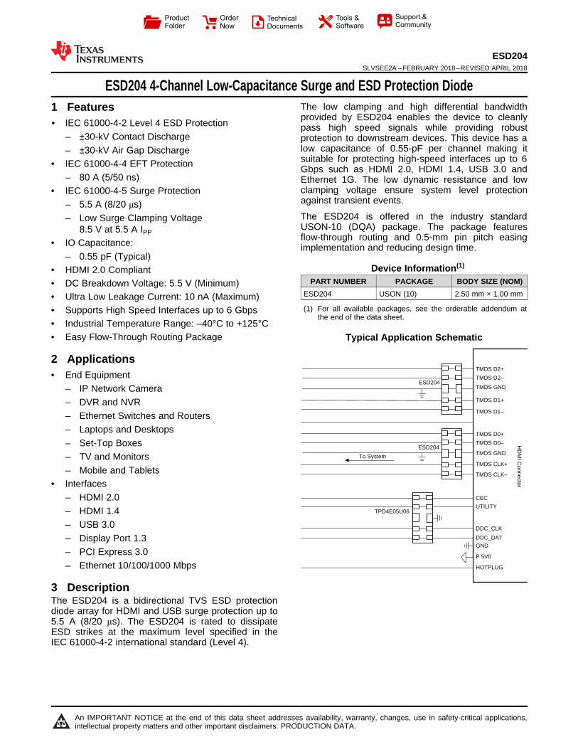
5 Pin Configuration and Functions
DQA Package10-Pin USON
Top View
Pin FunctionsPIN
TYPE DESCRIPTIONNAME NO.
GND 3Ground Ground. Connect to ground
GND 8IO1 1
I/O ESD protected channel. Connect to the line being protected.IO2 2IO3 4IO4 5NC 6
NC Not connected internally; Can be connected to line being protected for optional flow-through routing. Can also be left floating or grounded
NC 7NC 9NC 10

4
ESD204SLVSEE2A –FEBRUARY 2018–REVISED APRIL 2018 www.ti.com
Product Folder Links: ESD204
Submit Documentation Feedback Copyright © 2018, Texas Instruments Incorporated
(1) Stresses beyond those listed under Absolute Maximum Rating may cause permanent damage to the device. These are stress ratingsonly, which do not imply functional operation of the device at these or any other conditions beyond those indicated under RecommendedOperating Condition. Exposure to absolute-maximum-rated conditions for extended periods may affect device reliability.
6 Specifications
6.1 Absolute Maximum Ratingsover operating free-air temperature range (unless otherwise noted) (1)
MIN MAX UNITElectrical FastTransient IEC 61000-4-4 Peak Current at 25°C 80 A
Peak PulseIEC 61000-4-5 Surge (tp 8/20 µs) Peak Power at 25°C 50 WIEC 61000-4-5 Surge (tp 8/20 µs) Peak Current at 25°C 5.5 A
TA Operating free-air temperature -40 125 °CTstg Storage temperature -65 155 °C
(1) JEDEC document JEP155 states that 500-V HBM allows safe manufacturing with a standard ESD control process.(2) JEDEC document JEP157 states that 250-V CDM allows safe manufacturing with a standard ESD control process.
6.2 ESD Ratings -JEDEC SpecificationsVALUE UNIT
V(ESD) Electrostatic discharge
Human body model (HBM), perANSI/ESDA/JEDEC JS-001, all pins (1) ±2500
VCharged device model (CDM), per JEDECspecification JESD22-C101, all pins (2) ±1000
6.3 ESD Ratings - IEC SpecificationsVALUE UNIT
V(ESD) Electrostatic dischargeIEC 61000-4-2 Contact Discharge, all pins ±30000
VIEC 61000-4-2 Air Discharge, all pins ±30000
6.4 Recommended Operating Conditionsover operating free-air temperature range (unless otherwise noted)
MIN NOM MAX UNITVIN Input voltage -3.6 3.6 VTA Operating Free Air Temperature -40 125 °C
(1) For more information about traditional and new thermal metrics, see the Semiconductor and IC Package Thermal Metrics applicationreport.
6.5 Thermal Information
THERMAL METRIC (1)ESD204
UNITDQA (USON)10 PINS
RθJA Junction-to-ambient thermal resistance 262.1 °C/W
RθJC(top) Junction-to-case (top) thermal resistance 184.6 °C/W
RθJB Junction-to-board thermal resistance 138.2 °C/WΨJT Junction-to-top characterization parameter 41.8 °C/WΨJB Junction-to-board characterization parameter 137.8 °C/WRθJC(bot) Junction-to-case (bottom) thermal resistance N/A
5
ESD204www.ti.com SLVSEE2A –FEBRUARY 2018–REVISED APRIL 2018
Product Folder Links: ESD204
Submit Documentation FeedbackCopyright © 2018, Texas Instruments Incorporated
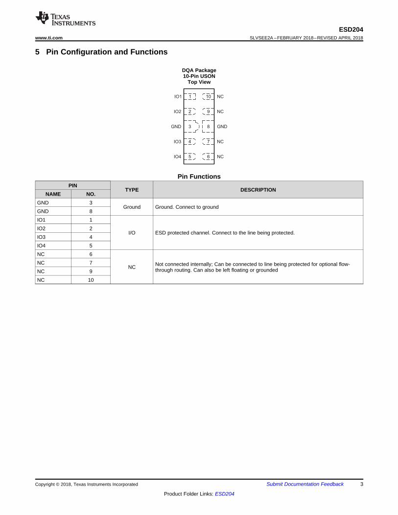
(1) VBRF and VBRR are defined as the voltage obtained at 1 mA when sweeping the voltage up, before the device latches into the snapbackstate
(2) VHOLD is defined as the voltage when 1 mA is applied, after the device has successfully latched into the snapback state.
6.6 Electrical CharacteristicsAt TA = 25°C unless otherwise noted
PARAMETER TEST CONDITIONS MIN TYP MAX UNIT
VRWM Reverse stand-off voltage IIO < 10 nA, across operatingtemperature range -3.6 3.6 V
VBRFPositive Breakdown Voltage, Each IOPin to GND (1) IIO = 1 mA 5 7.9 V
VBRRNegative Breakdown Voltage, Each IOPin to GND (1) IIO = -1 mA, -7.9 -5 V
VHOLD Positive Holding Voltage, Each IO pinto GND (2)
IIO = 1 mA 6.2 V
VHOLD-NEGNegative Holding Voltage, Each IOpin to GND (2) IIO = -1 mA -6.2 V
VCLAMP Clamping voltage
Surge IPP = 5.5 A, Each IO pin toGND, GND to Each IO pin, tp=8/20 μs 8.5 V
TLP IPP = 5 A, Each IO pin to GND,GND to Each IO pin, tp=10/100 ns 8.2 V
TLP IPP = 16 A, Each IO pin to GND,GND to Each IO pin, tp=10/100 ns 11.5 V
RDYN Dynamic resistance
Each IO Pin to GND, TLP tp=10/100ns 0.3
ΩGND to Each IO Pin, TLP tp=10/100ns 0.3
CLINE Line capacitance, any IO to GND VIO = 0 V, Vp-p = 30 mV, f = 1 MHz 0.55 0.65 pF
ΔCLINE Variation of line capacitance CLINE1 - CLINE2, VIO = 0 V, Vp-p = 30mV, f = 1 MHz 0.02 0.07 pF
CCROSS Line-to-line capacitance VIO = 0 V, Vrms = 30 mV, f = 1 MHz 0.25 0.35 pF

Time (ns)
Vol
tage
(V
)
-10 0 10 20 30 40 50 60 70 80 90-120-110-100
-90-80-70-60-50-40-30-20-10
01020
D004 Bias Voltage (V)
Cap
acita
nce
(pF
)
0 0.5 1 1.5 2 2.5 3 3.5 40
0.1
0.2
0.3
0.4
0.5
0.6
0.7
0.8
D008D008
Time (us)
Cur
rent
(A
)
Pow
er (
W)
0 20 40 60 80 100 120 140 160 180 2000 -5
0.5 0
1 5
1.5 10
2 15
2.5 20
3 25
3.5 30
4 35
4.5 40
5 45
5.5 50
6 55
D006
Current (A)Power (W)
Time (ns)
Vol
tage
(V
)
-10 0 10 20 30 40 50 60 70 80 90 100-20
-10
0
10
20
30
40
50
60
70
80
90
100
110
D003D003
Voltage (V)
Cur
rent
(A
)
0 2 4 6 8 10 12 14 16-5
0
5
10
15
20
25
30
D001 Voltage (V)
Cur
rent
(A
)
0 2 4 6 8 10 12 14 16-5
0
5
10
15
20
25
30
D002
6
ESD204SLVSEE2A –FEBRUARY 2018–REVISED APRIL 2018 www.ti.com
Product Folder Links: ESD204
Submit Documentation Feedback Copyright © 2018, Texas Instruments Incorporated
6.7 Typical Characteristics
Figure 1. Positive TLP Curve, IO pin to GND (tp = 100 ns) Figure 2. Negative TLP Curve, GND to IO pin (tp=100 ns;Plotted as Positive TLP Curve from GND to IO pin)
Figure 3. Surge Curve (tp = 8/20 µs), any IO pin to GND Figure 4. 8-kV IEC 61000-4-2 Clamping Voltage Waveform,IO pin to GND
Figure 5. –8-kV IEC 61000-4-2 Clamping Voltage Waveform,GND pin to IO
Figure 6. Capacitance vs Bias Voltage

Frequency (GHz)
Cap
acita
nce
(pF
)
1 1.5 2 2.5 3 3.5 4 4.5 5 5.5 60
0.1
0.2
0.3
0.4
0.5
0.6
0.7
ESD2D010 Frequency (Ghz)
Sdd
21 (
dB)
0.1 0.2 0.3 0.5 0.7 1 2 3 4 5 6 7 8 10-10
-9
-8
-7
-6
-5
-4
-3
-2
-1
0
1
D009
Temperature (qC)
Leak
age
Cur
rent
(nA
)
-40 -20 0 20 40 60 80 100 120 1400
0.3
0.6
0.9
1.2
1.5
1.8
2.1
D007 Voltage (V)
Cur
rent
(A
)
-8 -7 -6 -5 -4 -3 -2 -1 0 1 2 3 4 5 6 7 8-0.001
-0.0005
0
0.0005
0.001
D005D005
7
ESD204www.ti.com SLVSEE2A –FEBRUARY 2018–REVISED APRIL 2018
Product Folder Links: ESD204
Submit Documentation FeedbackCopyright © 2018, Texas Instruments Incorporated
Typical Characteristics (continued)
Figure 7. Leakage Current vs Temperature, IO pin to GND at3.6 V Bias
Figure 8. DC Voltage Sweep I-V Curve, IO pin to GND
Figure 9. Capacitance vs Frequency Figure 10. Differential Insertion Loss
IO4
GND
IO3IO2IO1
8
ESD204SLVSEE2A –FEBRUARY 2018–REVISED APRIL 2018 www.ti.com
Product Folder Links: ESD204
Submit Documentation Feedback Copyright © 2018, Texas Instruments Incorporated
7 Detailed Description
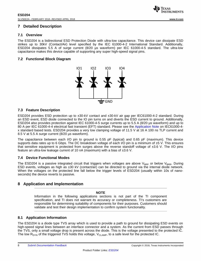
7.1 OverviewThe ESD204 is a bidirectional ESD Protection Diode with ultra-low capacitance. This device can dissipate ESDstrikes up to 30kV (Contact/Air) level specified by the IEC 61000-4-2 International Standard. Additionally,ESD204 dissipates 5.5 A of surge current (8/20 µs waveform) per IEC 61000-4-5 standard. The ultra-lowcapacitance makes this device capable of supporting any super high-speed signal pins.
7.2 Functional Block Diagram
7.3 Feature DescriptionESD204 provides ESD protection up to ±30-kV contact and ±30-kV air gap per IEC61000-4-2 standard. Duringan ESD event, ESD diode connected to the IO pin turns on and diverts the ESD current to ground. Additionally,ESD204 also provides protection against IEC 61000-4-5 surge currents up to 5.5 A (8/20 µs waveform) and up to80 A per IEC 61000-4-4 electrical fast transient (EFT) standard. Please see the Application Note on IEC61000-4-x standard based tests. ESD204 provides a very low clamping voltage of 11.5 V at 16 A 100 ns TLP current and8.5 V at 5.5 A surge current (8/20 µs waveform).
The capacitance between each I/O pin to ground is 0.55 pF (typical) and 0.65 pF (maximum). This devicesupports data rates up to 6 Gbps. The DC breakdown voltage of each I/O pin is a minimum of ±5 V. This ensuresthat sensitive equipment is protected from surges above the reverse standoff voltage of ±3.6 V. The I/O pinsfeature an ultra-low leakage current of 10 nA (maximum) with a bias of ±3.6 V.
7.4 Device Functional ModesThe ESD204 is a passive integrated circuit that triggers when voltages are above VBRF or below VBRR. DuringESD events, voltages as high as ±30 kV (contact/air) can be directed to ground via the internal diode network.When the voltages on the protected line fall below the trigger levels of ESD204 (usually within 10s of nano-seconds) the device reverts to passive.
8 Application and Implementation
NOTEInformation in the following applications sections is not part of the TI componentspecification, and TI does not warrant its accuracy or completeness. TI’s customers areresponsible for determining suitability of components for their purposes. Customers shouldvalidate and test their design implementation to confirm system functionality.
8.1 Application InformationThe ESD204 is a diode type TVS array which is used to provide a path to ground for dissipating ESD events onhigh-speed signal lines between an interface connector and a system. As the current from ESD passes throughthe TVS, only a small voltage drop is present across the diode. This is the voltage presented to the protected IC.The low RDYN of the triggered TVS holds this voltage, VCLAMP, to a safe level for the protected IC.

HD
MI C
onnector
HOTPLUG
UTILITY
TMDS D2+
CEC
DDC_CLK
DDC_DAT
TMDS D0±
TMDS CLK+
TMDS D1+
TMDS D1±
TMDS D0+
TMDS CLK±
TMDS D2±
P 5V0
GND
To System
TMDS GND
TMDS GND
ESD204
ESD204
TPD4E05U06
9
ESD204www.ti.com SLVSEE2A –FEBRUARY 2018–REVISED APRIL 2018
Product Folder Links: ESD204
Submit Documentation FeedbackCopyright © 2018, Texas Instruments Incorporated
8.2 Typical Application
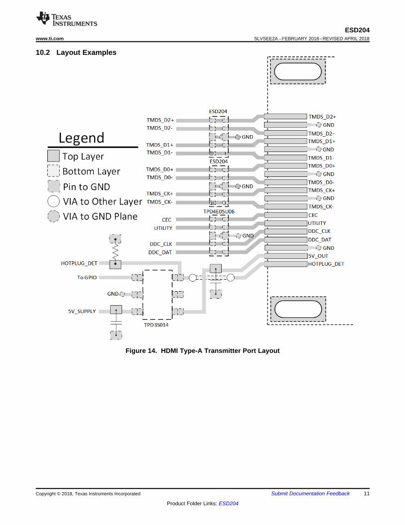
Figure 11. ESD204 Protecting the HDMI Interface
8.2.1 Design RequirementsIn this design example, two ESD204 devices and one TPD4E05U06 device are used to protect an HDMI 2.0interface. For HDMI 2.0 application design parameters listed in Table 1 are known.
Table 1. Design ParametersDESIGN PARAMETER VALUE
Signal range on high speed differential datalines 0 to 3.6 V
Operating frequency of high speed data lines 3 GHz (First Harmonic)Signal range on control lines (CEC, UTILITY,
DDC_CLK and DDC_DAT) 0 to 5 V
8.2.2 Detailed Design Procedure
8.2.2.1 Signal RangeESD204 supports signal ranges between –3.6 V and 3.6 V, which supports the high-speed lines on the HDMI 2.0application. The TPD4E05U06 supports signal ranges between 0 V and 5.5 V, which supports the HDMI controllines.
8.2.2.2 Operating FrequencyThe ESD204 has a 0.55 pF (typical) capacitance, which supports the HDMI 2.0 rate of 6 Gbps. TheTPD4E05U06 has a typical capacitance of 0.5 pF, which easily support the control lines. The ESD204 has 4identical protection channels for the differential HDMI high-speed signal lines. The symmetrical pin out of thedevice with a ground pin between the two differential signal pins makes it suitable for this application.
10
ESD204SLVSEE2A –FEBRUARY 2018–REVISED APRIL 2018 www.ti.com
Product Folder Links: ESD204
Submit Documentation Feedback Copyright © 2018, Texas Instruments Incorporated
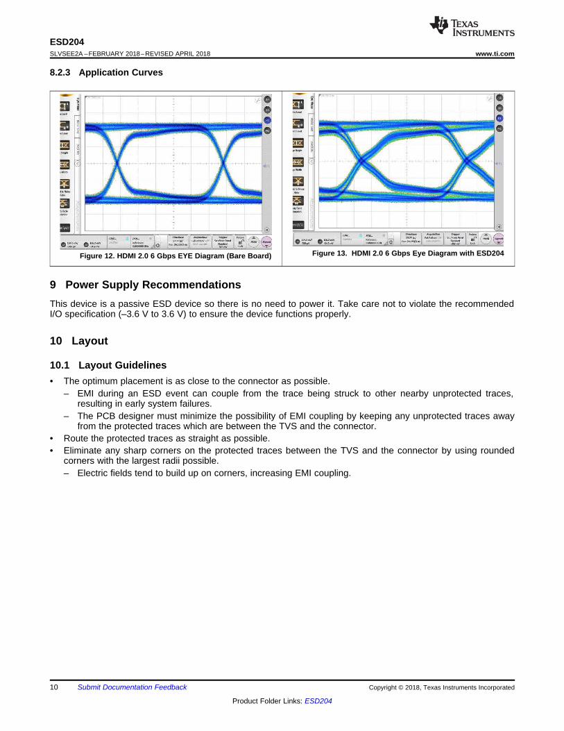
8.2.3 Application Curves
Figure 12. HDMI 2.0 6 Gbps EYE Diagram (Bare Board) Figure 13. HDMI 2.0 6 Gbps Eye Diagram with ESD204
9 Power Supply RecommendationsThis device is a passive ESD device so there is no need to power it. Take care not to violate the recommendedI/O specification (–3.6 V to 3.6 V) to ensure the device functions properly.
10 Layout
10.1 Layout Guidelines• The optimum placement is as close to the connector as possible.
– EMI during an ESD event can couple from the trace being struck to other nearby unprotected traces,resulting in early system failures.
– The PCB designer must minimize the possibility of EMI coupling by keeping any unprotected traces awayfrom the protected traces which are between the TVS and the connector.
• Route the protected traces as straight as possible.• Eliminate any sharp corners on the protected traces between the TVS and the connector by using rounded
corners with the largest radii possible.– Electric fields tend to build up on corners, increasing EMI coupling.
11
ESD204www.ti.com SLVSEE2A –FEBRUARY 2018–REVISED APRIL 2018
Product Folder Links: ESD204
Submit Documentation FeedbackCopyright © 2018, Texas Instruments Incorporated
10.2 Layout Examples
Figure 14. HDMI Type-A Transmitter Port Layout
12
ESD204SLVSEE2A –FEBRUARY 2018–REVISED APRIL 2018 www.ti.com
Product Folder Links: ESD204
Submit Documentation Feedback Copyright © 2018, Texas Instruments Incorporated
11 Device and Documentation Support
11.1 Receiving Notification of Documentation UpdatesTo receive notification of documentation updates, navigate to the device product folder on ti.com. In the upperright corner, click on Alert me to register and receive a weekly digest of any product information that haschanged. For change details, review the revision history included in any revised document.
11.2 Community ResourcesThe following links connect to TI community resources. Linked contents are provided "AS IS" by the respectivecontributors. They do not constitute TI specifications and do not necessarily reflect TI's views; see TI's Terms ofUse.
TI E2E™ Online Community TI's Engineer-to-Engineer (E2E) Community. Created to foster collaborationamong engineers. At e2e.ti.com, you can ask questions, share knowledge, explore ideas and helpsolve problems with fellow engineers.
Design Support TI's Design Support Quickly find helpful E2E forums along with design support tools andcontact information for technical support.
11.3 TrademarksE2E is a trademark of Texas Instruments.All other trademarks are the property of their respective owners.
11.4 Electrostatic Discharge CautionThis integrated circuit can be damaged by ESD. Texas Instruments recommends that all integrated circuits be handled withappropriate precautions. Failure to observe proper handling and installation procedures can cause damage.
ESD damage can range from subtle performance degradation to complete device failure. Precision integrated circuits may be moresusceptible to damage because very small parametric changes could cause the device not to meet its published specifications.
11.5 GlossarySLYZ022 — TI Glossary.
This glossary lists and explains terms, acronyms, and definitions.
12 Mechanical, Packaging, and Orderable InformationThe following pages include mechanical, packaging, and orderable information. This information is the mostcurrent data available for the designated devices. This data is subject to change without notice and revision ofthis document. For browser-based versions of this data sheet, refer to the left-hand navigation.

PACKAGE OPTION ADDENDUM
www.ti.com 10-Dec-2020
Addendum-Page 1
PACKAGING INFORMATION
Orderable Device Status(1)
Package Type PackageDrawing
Pins PackageQty
Eco Plan(2)
Lead finish/Ball material
(6)
MSL Peak Temp(3)
Op Temp (°C) Device Marking(4/5)
Samples
ESD204DQAR ACTIVE USON DQA 10 3000 RoHS & Green NIPDAU Level-1-260C-UNLIM -40 to 125 CEGCEY
(1) The marketing status values are defined as follows:ACTIVE: Product device recommended for new designs.LIFEBUY: TI has announced that the device will be discontinued, and a lifetime-buy period is in effect.NRND: Not recommended for new designs. Device is in production to support existing customers, but TI does not recommend using this part in a new design.PREVIEW: Device has been announced but is not in production. Samples may or may not be available.OBSOLETE: TI has discontinued the production of the device.
(2) RoHS: TI defines "RoHS" to mean semiconductor products that are compliant with the current EU RoHS requirements for all 10 RoHS substances, including the requirement that RoHS substancedo not exceed 0.1% by weight in homogeneous materials. Where designed to be soldered at high temperatures, "RoHS" products are suitable for use in specified lead-free processes. TI mayreference these types of products as "Pb-Free".RoHS Exempt: TI defines "RoHS Exempt" to mean products that contain lead but are compliant with EU RoHS pursuant to a specific EU RoHS exemption.Green: TI defines "Green" to mean the content of Chlorine (Cl) and Bromine (Br) based flame retardants meet JS709B low halogen requirements of <=1000ppm threshold. Antimony trioxide basedflame retardants must also meet the <=1000ppm threshold requirement.
(3) MSL, Peak Temp. - The Moisture Sensitivity Level rating according to the JEDEC industry standard classifications, and peak solder temperature.
(4) There may be additional marking, which relates to the logo, the lot trace code information, or the environmental category on the device.
(5) Multiple Device Markings will be inside parentheses. Only one Device Marking contained in parentheses and separated by a "~" will appear on a device. If a line is indented then it is a continuationof the previous line and the two combined represent the entire Device Marking for that device.
(6) Lead finish/Ball material - Orderable Devices may have multiple material finish options. Finish options are separated by a vertical ruled line. Lead finish/Ball material values may wrap to twolines if the finish value exceeds the maximum column width.
Important Information and Disclaimer:The information provided on this page represents TI's knowledge and belief as of the date that it is provided. TI bases its knowledge and belief on informationprovided by third parties, and makes no representation or warranty as to the accuracy of such information. Efforts are underway to better integrate information from third parties. TI has taken andcontinues to take reasonable steps to provide representative and accurate information but may not have conducted destructive testing or chemical analysis on incoming materials and chemicals.TI and TI suppliers consider certain information to be proprietary, and thus CAS numbers and other limited information may not be available for release.
In no event shall TI's liability arising out of such information exceed the total purchase price of the TI part(s) at issue in this document sold by TI to Customer on an annual basis.
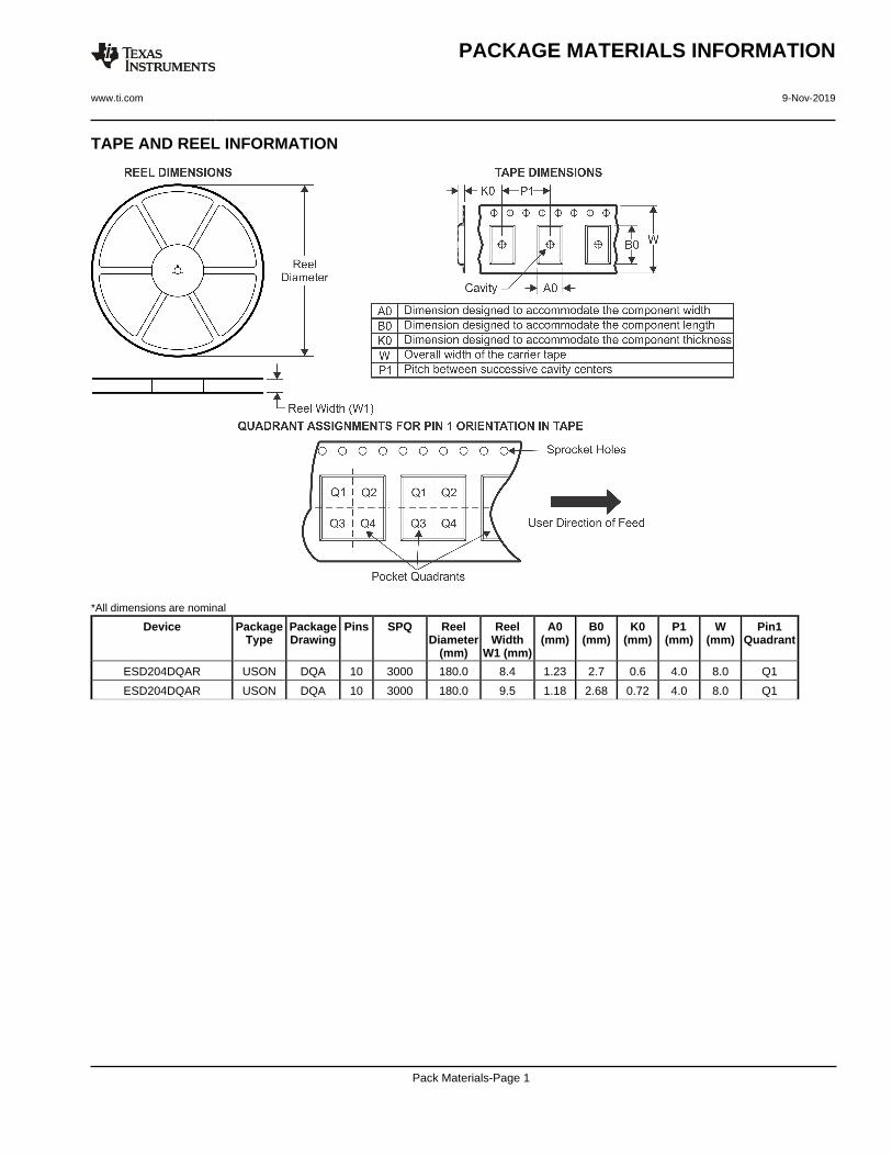
TAPE AND REEL INFORMATION
*All dimensions are nominal
Device PackageType
PackageDrawing
Pins SPQ ReelDiameter
(mm)
ReelWidth
W1 (mm)
A0(mm)
B0(mm)
K0(mm)
P1(mm)
W(mm)
Pin1Quadrant
ESD204DQAR USON DQA 10 3000 180.0 8.4 1.23 2.7 0.6 4.0 8.0 Q1
ESD204DQAR USON DQA 10 3000 180.0 9.5 1.18 2.68 0.72 4.0 8.0 Q1
PACKAGE MATERIALS INFORMATION
www.ti.com 9-Nov-2019
Pack Materials-Page 1

*All dimensions are nominal
Device Package Type Package Drawing Pins SPQ Length (mm) Width (mm) Height (mm)
ESD204DQAR USON DQA 10 3000 203.2 196.8 33.3
ESD204DQAR USON DQA 10 3000 189.0 185.0 36.0
PACKAGE MATERIALS INFORMATION
www.ti.com 9-Nov-2019
Pack Materials-Page 2
www.ti.com
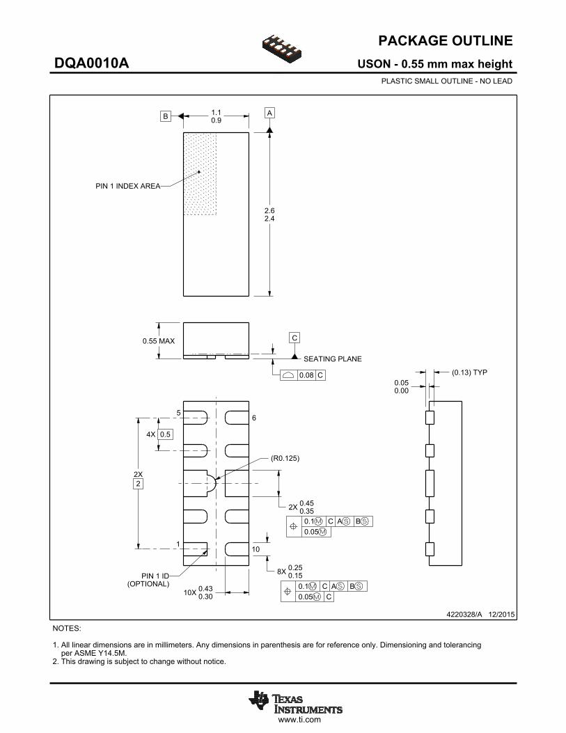
PACKAGE OUTLINE
C
8X 0.250.15
10X 0.430.30
2X2
4X 0.5
0.55 MAX
0.050.00
2X 0.450.35
B 1.10.9
A
2.62.4
(0.13) TYP
(R )0.125
USON - 0.55 mm max heightDQA0010APLASTIC SMALL OUTLINE - NO LEAD
4220328/A 12/2015
PIN 1 INDEX AREA
SEATING PLANE
0.08 C
1
56
10
(OPTIONAL)PIN 1 ID
0.1 C A B0.05 C
0.1 C A B0.05
NOTES: 1. All linear dimensions are in millimeters. Any dimensions in parenthesis are for reference only. Dimensioning and tolerancing per ASME Y14.5M. 2. This drawing is subject to change without notice.
SCALE 6.000

www.ti.com
EXAMPLE BOARD LAYOUT
0.07 MINALL AROUND
0.07 MAXALL AROUND
4X (0.5)
(0.835)
8X (0.2)
10X (0.565)
(R ) TYP0.05
2X (0.4)
USON - 0.55 mm max heightDQA0010APLASTIC SMALL OUTLINE - NO LEAD
4220328/A 12/2015
SYMM
1
56
10
SYMM
LAND PATTERN EXAMPLESCALE:30X
NOTES: (continued) 3. For more information, see Texas Instruments literature number SLUA271 (www.ti.com/lit/slua271).
SOLDER MASKOPENINGSOLDER MASK
METAL UNDER
SOLDER MASKDEFINED
METALSOLDER MASKOPENING
SOLDER MASK DETAILS
NON SOLDER MASKDEFINED
(PREFERRED)

www.ti.com
EXAMPLE STENCIL DESIGN
8X (0.2)
10X (0.565)
4X (0.5)
2X (0.36)
(0.835)
(R ) TYP0.05
USON - 0.55 mm max heightDQA0010APLASTIC SMALL OUTLINE - NO LEAD
4220328/A 12/2015
NOTES: (continued) 4. Laser cutting apertures with trapezoidal walls and rounded corners may offer better paste release. IPC-7525 may have alternate design recommendations.
SOLDER PASTE EXAMPLEBASED ON 0.1 mm THICK STENCIL
EXPOSED PADS 3 & 8:
90% PRINTED SOLDER COVERAGE BY AREA UNDER PACKAGESCALE:40X
SYMM
1
56
10
SYMM
METALTYP
3 8

IMPORTANT NOTICE AND DISCLAIMER
TI PROVIDES TECHNICAL AND RELIABILITY DATA (INCLUDING DATASHEETS), DESIGN RESOURCES (INCLUDING REFERENCE DESIGNS), APPLICATION OR OTHER DESIGN ADVICE, WEB TOOLS, SAFETY INFORMATION, AND OTHER RESOURCES “AS IS” AND WITH ALL FAULTS, AND DISCLAIMS ALL WARRANTIES, EXPRESS AND IMPLIED, INCLUDING WITHOUT LIMITATION ANY IMPLIED WARRANTIES OF MERCHANTABILITY, FITNESS FOR A PARTICULAR PURPOSE OR NON-INFRINGEMENT OF THIRD PARTY INTELLECTUAL PROPERTY RIGHTS.These resources are intended for skilled developers designing with TI products. You are solely responsible for (1) selecting the appropriate TI products for your application, (2) designing, validating and testing your application, and (3) ensuring your application meets applicable standards, and any other safety, security, or other requirements. These resources are subject to change without notice. TI grants you permission to use these resources only for development of an application that uses the TI products described in the resource. Other reproduction and display of these resources is prohibited. No license is granted to any other TI intellectual property right or to any third party intellectual property right. TI disclaims responsibility for, and you will fully indemnify TI and its representatives against, any claims, damages, costs, losses, and liabilities arising out of your use of these resources.TI’s products are provided subject to TI’s Terms of Sale (www.ti.com/legal/termsofsale.html) or other applicable terms available either on ti.com or provided in conjunction with such TI products. TI’s provision of these resources does not expand or otherwise alter TI’s applicable warranties or warranty disclaimers for TI products.
Mailing Address: Texas Instruments, Post Office Box 655303, Dallas, Texas 75265Copyright © 2020, Texas Instruments Incorporated
Related Documents