MEASUREMENT SCIENCE REVIEW, Volume 14, No. 2, 2014 62 Error Models of the Analog to Digital Converters Linus Michaeli, Ján Šaliga Dept. of Electronics and Multimedia Communications, Technical University of Kosice, Letna 9/A, 04120 Košice, Slovakia (linus.michaeli, jan.saliga)@tuke.sk Error models of the Analog to Digital Converters describe metrological properties of the signal conversion from analog to digital domain in a concise form using few dominant error parameters. Knowledge of the error models allows the end user to provide fast testing in the crucial points of the full input signal range and to use identified error models for post correction in the digital domain. The imperfections of the internal ADC structure determine the error characteristics represented by the nonlinearities as a function of the output code. Progress in the microelectronics and missing information about circuital details together with the lack of knowledge about interfering effects caused by ADC installation prefers another modeling approach based on the input-output behavioral characterization by the input-output error box. Internal links in the ADC structure cause that the input-output error function could be described in a concise form by suitable function. Modeled functional parameters allow determining the integral error parameters of ADC. Paper is a survey of error models starting from the structural models for the most common architectures and their linkage with the behavioral models represented by the simple look up table or the functional description of nonlinear errors for the output codes. Keywords: ADC testing, ADC modeling, data correction. 1. INTRODUCTION NALOG TO Digital Converters (ADC) or Digital to Analog Converters (DAC) are the key components performing interrelation and conversion between the analog and digital worlds. Quality of analog quantity conversion into its digital representation is characterized by the error parameters of ADC. These parameters are in the form of either functional error parameters such as integral nonlinearity (INL(k)) and differential nonlinearity (DNL(k)) or integral errors such as signal to noise and distortion ratio (SINAD), total harmonic distortion (THD), effective number of bits (ENOB), etc. The functional error parameters describe deviations between ideal and real transfer characteristics as functions of the output code k. The integral error parameters describe conversion quality using simple numbers, and some of them can be mathematically derived from ADC transfer functions. Error parameters are the necessary basis for designing any proper error model. Their deeper description and definition is beyond the scope of this article, however, and can be found in the relevant standards [1], [2]. Error models of ADC represent a comprehensive tool presenting the impact of the real converter on the metrological quality of the analog to digital conversion. The error models describe nonlinearities in the crucial points within the converter’s range. The measured errors in the selected points allow estimating the error parameters, functional and integral, over the full range. Identified error models of ADCs are suitable for: • sub-circuit description in CAD simulators for the assessment of uncertainty and for evaluation of the implemented post-correction procedure [50]. • estimation of other integral error parameters of ADC, such as THD and SINAD, by simulation for any stimulus signal [30], [46]. • implementation of the fast ADC testing which is focused on the identification of the dominant error sources exceeding accessible testing uncertainty. Because of increasing resolution and quality of ADCs, end-users prefer to focus on the dominant error sources and their extrapolation by the error models. The fast ADC testing procedures allow reaching this objective faster than it is possible by the standardized testing procedures [5], [41-42]. In the following article, a brief classification of ADC models is given in Section 2. Structural error models for the most popular ADC architectures are derived and experimentally verified in Section 3. Based on the study provided in the previous section, behavioral models are presented in Section 4. 2. CLASSIFICATION OF THE ADC ERROR MODELS Error models of ADC can be classified as architecture- dependent models or as behavioral models (generic black box models) identified by the input- output characteristics. The most precise description is the one at the lowest level covering all circuit components, the interconnections among them, and the stray parasitic capacities determined by the position of circuits on the chip and printed board. This description is represented in the circuit-level electrical models. These models comprise the utilized technology with its impact on the component parameters and are included in the Computer Aided Design (CAD) systems. Circuit-level models are the most precise tool for the limited group of component and system designers. Electrical structural models describe ADC error characteristics through simplified equivalent circuits or functional blocks performing the conversion. They represent a compromise between accuracy resulting from the circuit level description and simplicity coming from knowledge of the internal architecture together with the dominant error sources. The most general description of the ADC error properties is presented in the behavioral error model, which does not take into account the physical realization of ADC at all. A 10.2478/msr-2014-0010

Welcome message from author
This document is posted to help you gain knowledge. Please leave a comment to let me know what you think about it! Share it to your friends and learn new things together.
Transcript

MEASUREMENT SCIENCE REVIEW, Volume 14, No. 2, 2014
62
Error Models of the Analog to Digital Converters
Linus Michaeli, Ján Šaliga
Dept. of Electronics and Multimedia Communications, Technical University of Kosice, Letna 9/A, 04120 Košice, Slovakia (linus.michaeli, jan.saliga)@tuke.sk
Error models of the Analog to Digital Converters describe metrological properties of the signal conversion from analog to digital
domain in a concise form using few dominant error parameters. Knowledge of the error models allows the end user to provide fast
testing in the crucial points of the full input signal range and to use identified error models for post correction in the digital
domain. The imperfections of the internal ADC structure determine the error characteristics represented by the nonlinearities as a
function of the output code. Progress in the microelectronics and missing information about circuital details together with the lack
of knowledge about interfering effects caused by ADC installation prefers another modeling approach based on the input-output
behavioral characterization by the input-output error box. Internal links in the ADC structure cause that the input-output error
function could be described in a concise form by suitable function. Modeled functional parameters allow determining the integral
error parameters of ADC. Paper is a survey of error models starting from the structural models for the most common
architectures and their linkage with the behavioral models represented by the simple look up table or the functional description of
nonlinear errors for the output codes.
Keywords: ADC testing, ADC modeling, data correction.
1. INTRODUCTION
NALOG TO Digital Converters (ADC) or Digital to Analog Converters (DAC) are the key components performing interrelation and conversion between the
analog and digital worlds. Quality of analog quantity conversion into its digital representation is characterized by the error parameters of ADC. These parameters are in the form of either functional error parameters such as integral nonlinearity (INL(k)) and differential nonlinearity (DNL(k)) or integral errors such as signal to noise and distortion ratio (SINAD), total harmonic distortion (THD), effective number of bits (ENOB), etc. The functional error parameters describe deviations between ideal and real transfer characteristics as functions of the output code k. The integral error parameters describe conversion quality using simple numbers, and some of them can be mathematically derived from ADC transfer functions. Error parameters are the necessary basis for designing any proper error model. Their deeper description and definition is beyond the scope of this article, however, and can be found in the relevant standards [1], [2].
Error models of ADC represent a comprehensive tool presenting the impact of the real converter on the metrological quality of the analog to digital conversion. The error models describe nonlinearities in the crucial points within the converter’s range. The measured errors in the selected points allow estimating the error parameters, functional and integral, over the full range.
Identified error models of ADCs are suitable for: • sub-circuit description in CAD simulators for the
assessment of uncertainty and for evaluation of the implemented post-correction procedure [50].
• estimation of other integral error parameters of ADC, such as THD and SINAD, by simulation for any stimulus signal [30], [46].
• implementation of the fast ADC testing which is focused on the identification of the dominant error sources
exceeding accessible testing uncertainty. Because of increasing resolution and quality of ADCs, end-users prefer to focus on the dominant error sources and their extrapolation by the error models. The fast ADC testing procedures allow reaching this objective faster than it is possible by the standardized testing procedures [5], [41-42].
In the following article, a brief classification of ADC models is given in Section 2. Structural error models for the most popular ADC architectures are derived and experimentally verified in Section 3. Based on the study provided in the previous section, behavioral models are presented in Section 4.
2. CLASSIFICATION OF THE ADC ERROR MODELS
Error models of ADC can be classified as architecture-dependent models or as behavioral models (generic black box models) identified by the input- output characteristics.
The most precise description is the one at the lowest level covering all circuit components, the interconnections among them, and the stray parasitic capacities determined by the position of circuits on the chip and printed board. This description is represented in the circuit-level electrical models. These models comprise the utilized technology with its impact on the component parameters and are included in the Computer Aided Design (CAD) systems. Circuit-level models are the most precise tool for the limited group of component and system designers.
Electrical structural models describe ADC error characteristics through simplified equivalent circuits or functional blocks performing the conversion. They represent a compromise between accuracy resulting from the circuit level description and simplicity coming from knowledge of the internal architecture together with the dominant error sources.
The most general description of the ADC error properties is presented in the behavioral error model, which does not take into account the physical realization of ADC at all.
A
10.2478/msr-2014-0010

MEASUREMENT SCIENCE REVIEW, Volume 14, No. 2, 2014
63
The device is characterized by the input- output analytical or numerical relation, without going deep into the internal structure. The advantage of any behavioral model is the description of random errors like noise, jitter or glitches, as additional information to the systematic errors (INL(k), DNL(k)).
Fig.1. Classification of the ADC error models.
Error modeling is generally approached with an “à-priori”
or “à-posteriori” strategy [27]. The first strategy exploits available information on error source influences inside the conversion mechanism and/or architecture. The “à-posteriori” strategy utilizes only the data from experimental tests. They serve for the identification of the appropriate mathematical description.
Furthermore, a different model classification can be carried out according to the static or dynamic nature of the errors. Static models characterize the converter based on a constant input signal, whereas dynamic models consider a variable input signal. Time variation in the input signal is often suppressed by the sample and hold circuit at the input of ADC. The static model best describes this situation.
Besides Analog to Digital and Digital to Analog Converters, the Data Acquisition Systems (DAQ) may employ one or more of the following circuit blocks: buffering amplifier, filters, nonlinear analog blocks, sample and hold circuit and analog switches. All those analog blocks are critical components. The analog input signal is influenced by a wide range of external and internal error effects which have an impact on the transfer function error. Weak possibility to reduce parasitic effects in the conditioning blocks is the main motivation for the system designers to reduce analog processing blocks to a minimum. Modeling of analog conditioning blocks is out of scope of this chapter. Proposals for the structural modeling of basic analog blocks are analyzed in [18-21],[23-27].
3. ADC STRUCTURAL ERROR MODELS
The most suitable ADC architectures for the structural error modeling are integrating ADC (I ADC), successive-approximation ADC (SAR ADC) and cyclic ADC (C ADC).
Their error models are strongly influenced by the conversion mechanism taking into account the dominant error sources inside their architecture. Sigma delta ADC (Σ∆ ADC) can be modeled similarly by the structure consisting of hardware and signal processing blocks.
3.1. THE INTEGRATING ADC.
The integrating ADCs represent a wide range of conversion architectures, where the analog input signal x is transformed in the Analog Processing Section (APS) on the selected parameter of the intermediate pulse train represented by the pulse width Tx or frequency fx (Fig.2.). The averaged value of the frequency of the digital pulses fx or the averaged pulse width Tx in the conversion time interval T are measured in the Quantizing Section (QS) and converted to output code k.
Fig.2. Basic structure of integrating ADC.
The structural error model of the integrating ADC is
derived for the most popular architecture represented by the Dual Slope ADC (DS ADC) (Fig.2.). The conversion is performed in two phases. The input signal x amplified in the buffering amplifier (OA) is connected through the analog switch (SW) to the input of the integrator (INT) and integrated in the constant interval T from the zero level on the voltage in the first phase. During the second phase the integrator is discharged by the current generated by the reference voltage. Discharging time interval Tx is terminated in the instant when the output voltage of integrator achieves the zero voltage level. End of interval is determined by the same comparator (COM). The time interval Tx is equal to the first formula in (1). Finally, the actual time interval Tx is converted into a digital code k in the Quantizing Section (QS) [3], [47]. The time measurement implements the classical approach based on the counting of the clock periods T0 during time interval Tx by the digital counter. It represents the rounding operation expressed by angular brackets. Removed part after decimal point represents the quantization noise.
=
==
00
xx ;
TV
xT
T
TkT
V
xT
REFREF
(1)
LkvsL
os QEff
f
2122
2 max =⇒>=
The well-known advantage of this structure is the
suppression of interfering signals superimposed on the input
„à-posteriori strategy“
Different level of abstraction „à-priori strategy“
ADC Error models
Architecture dependent error models
Circuit-level models
Behavioral ADC error models
Look up table models
Analytical In-Out relation
models
Structural error models
x
SW
.
INT
.
CO
M.
Tx xact xact
Analog Processing Section
QS Quantizing
Section
k
OA
.
VREF
fx
MEASUREMENT SCIENCE REVIEW, Volume 14, No. 2, 2014
64
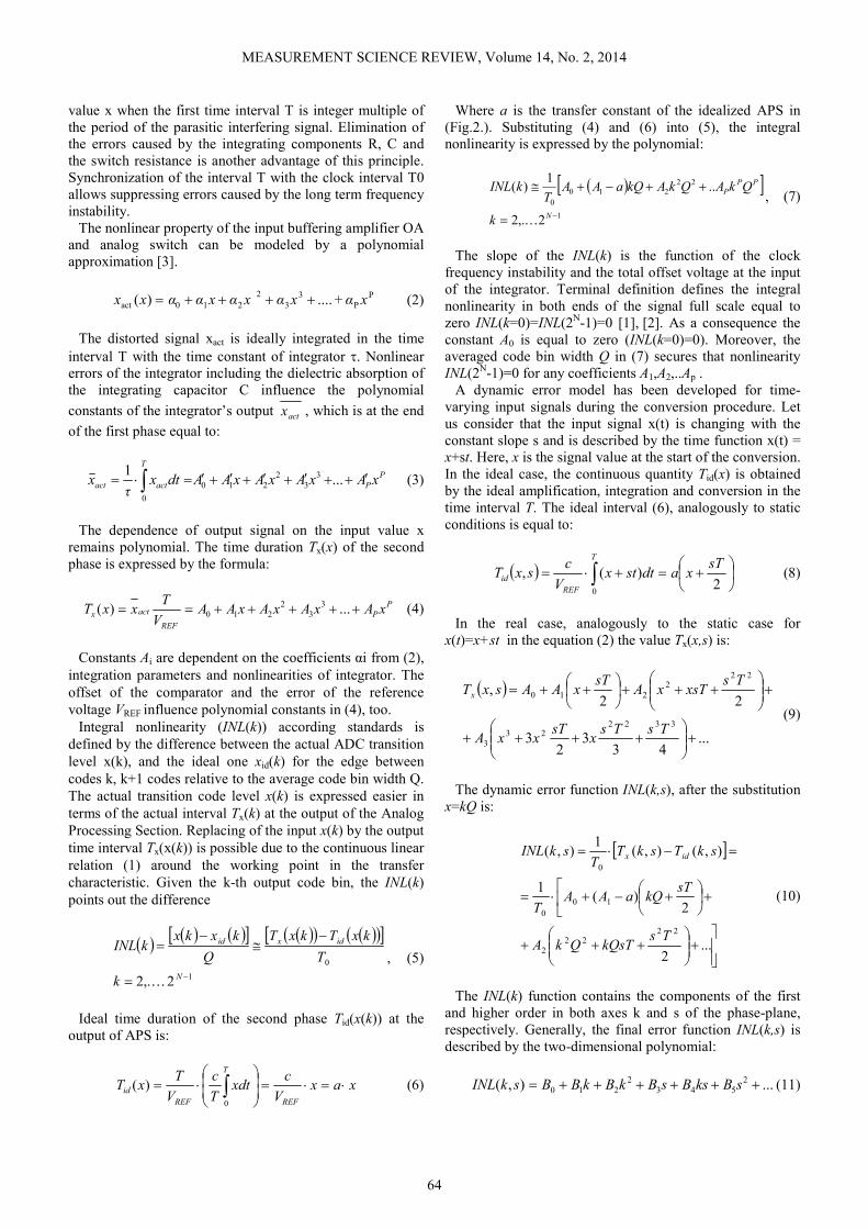
value x when the first time interval T is integer multiple of the period of the parasitic interfering signal. Elimination of the errors caused by the integrating components R, C and the switch resistance is another advantage of this principle. Synchronization of the interval T with the clock interval T0 allows suppressing errors caused by the long term frequency instability.
The nonlinear property of the input buffering amplifier OA and analog switch can be modeled by a polynomial approximation [3].
P
P3
32
210act +....)( xαxαxαxααxx ++++= (2)
The distorted signal xact is ideally integrated in the time
interval T with the time constant of integrator τ. Nonlinear errors of the integrator including the dielectric absorption of the integrating capacitor C influence the polynomial
constants of the integrator’s output actx , which is at the end
of the first phase equal to:
P
P
T
actact xAxAxAxAAdtxτ
x ′++′+′+′+′=⋅= ∫ ...1
0
33
2210 (3)
The dependence of output signal on the input value x
remains polynomial. The time duration Tx(x) of the second phase is expressed by the formula:
P
P
REF
actx xAxAxAxAAV
TxxT +++++== ...)( 3
32
210 (4)
Constants Ai are dependent on the coefficients αi from (2),
integration parameters and nonlinearities of integrator. The offset of the comparator and the error of the reference voltage VREF influence polynomial constants in (4), too.
Integral nonlinearity (INL(k)) according standards is defined by the difference between the actual ADC transition level x(k), and the ideal one xid(k) for the edge between codes k, k+1 codes relative to the average code bin width Q. The actual transition code level x(k) is expressed easier in terms of the actual interval Tx(k) at the output of the Analog Processing Section. Replacing of the input x(k) by the output time interval Tx(x(k)) is possible due to the continuous linear relation (1) around the working point in the transfer characteristic. Given the k-th output code bin, the INL(k) points out the difference
( ) ( ) ( )[ ] ( )( ) ( )( )[ ]
1
0
2,.2 −=
−≅
−=
N
idxid
k
T
kxTkxT
Q
kxkxkINL
K
, (5)
Ideal time duration of the second phase Tid(x(k)) at the
output of APS is:
xaxV
cxdt
T
c
V
TxT
REF
T
REF
id ⋅=⋅=
⋅= ∫
0
)( (6)
Where a is the transfer constant of the idealized APS in (Fig.2.). Substituting (4) and (6) into (5), the integral nonlinearity is expressed by the polynomial:
( )[ ]1
22210
0
2,.2
..1
)(
−=
++−+≅
N
PP
P
k
QkAQkAkQaAAT
kINL
K
, (7)
The slope of the INL(k) is the function of the clock
frequency instability and the total offset voltage at the input of the integrator. Terminal definition defines the integral nonlinearity in both ends of the signal full scale equal to zero INL(k=0)=INL(2N-1)=0 [1], [2]. As a consequence the constant A0 is equal to zero (INL(k=0)=0). Moreover, the averaged code bin width Q in (7) secures that nonlinearity INL(2N-1)=0 for any coefficients A1,A2,..Ap .
A dynamic error model has been developed for time-varying input signals during the conversion procedure. Let us consider that the input signal x(t) is changing with the constant slope s and is described by the time function x(t) = x+st. Here, x is the signal value at the start of the conversion. In the ideal case, the continuous quantity Tid(x) is obtained by the ideal amplification, integration and conversion in the time interval T. The ideal interval (6), analogously to static conditions is equal to:
( ) ∫
+=+⋅=
T
REF
id
sTxadtstx
V
csxT
02
)(, (8)
In the real case, analogously to the static case for
x(t)=x+st in the equation (2) the value Tx(x,s) is:
( )
...43
32
3
22,
332223
3
222
210
+
++++
+
+++
++=
TsTsx
sTxxA
TsxsTxA
sTxAAsxTx
(9)
The dynamic error function INL(k,s), after the substitution
x=kQ is:
[ ]
+
+++
+
+−+⋅=
=−⋅=
...2
2)(
1
),(),(1
),(
2222
2
100
0
TskQsTQkA
sTkQaAA
T
skTskTT
skINL idx
(10)
The INL(k) function contains the components of the first
and higher order in both axes k and s of the phase-plane, respectively. Generally, the final error function INL(k,s) is described by the two-dimensional polynomial:
...),( 2543
2210 ++++++= sBksBsBkBkBBskINL (11)

MEASUREMENT SCIENCE REVIEW, Volume 14, No. 2, 2014
65
Here, the coefficients related only to k (e.g., B0, B1, B2) represent the error behavior in the static case and they are proportional to A0, A1, A2, from (11). Vice versa, the coefficients related also to s (e.g., B3, B4, B5) extrapolate the dynamic effects due to the signal slope. Therefore, the error surface in the phase-plane k-s is modeled by a two dimensional polynomial (11), whose degree is generally low (2 or 3) [18]. The dynamic model of I ADC allows the error function to be divided in static INL1(k) and dynamic component INL2(k,s)
),()(),( 21 skINLkINLskINL += (12)
A. Extending the structural model for other ADC with
integration principle.
The common feature of all integrating ADCs is the intermediate linear conversion of the input signal x on the pulse width Tx or frequency fx. While the input APS performs conversion of the continuous input signal x into a selected parameter (frequency fx or pulse width Tx) of the intermediate binary train, the cascaded QS performs discretization of this parameter. Since the digital output data k from the QS represents the averaged value of the intermediate parameter, the output value k of the all integrating ADCs is proportional to the averaged value of input signal x (Fig.2.). Various I ADCs (single slope and multi slope ADCs, ADC with voltage to frequency converter, etc.) differ by the APS structure [31], [35]. Objective of these modifications is the suppression of a variety of the external error sources. The nonlinearity of operational amplifier, error parameters of the analog switches, imperfections of the integrator caused by its limited bandwidth and dielectric absorption of the feedback capacitor, offset of the comparator, etc. are the main error sources in the APS transfer function. The analog part remains always the main contributor to the whole conversion error.
B. Sigma delta ADC.
The structural model of a sigma-delta ADC (Σ∆ ADC) consists of the differential amplifier, cascaded integrator and the comparator, which detects polarity of the voltage at the output of the integrator. The output signal from the comparator compensates the input voltage x through one bit DAC in the instances given by clock CLK. The feedback keeps the output voltage of the integrator around zero level. This APS is Σ∆ modulator which converts input value x into the pulse train px. The mean value of the pulse density px is proportional to x in time interval T [33], [42].
The digital value k is obtained at the output of the digital LP filter which follows the Σ∆ modulator. The simplest digital LP filter is the pulse counter and represents the Quantizing Section. Resolution of the Σ∆ ADC can be controlled by setting of time interval T.
There is a variety of the modifications in Σ∆ feedback according to its order and parallelism which results in the differently effective suppression of the quantization noise at low frequencies. Offset and drift of the comparator are compensated by the feedback and they have no influence on
the final conversion error. Offset of the input amplifier and integrator cause the zero error at the beginning of the transfer characteristics. The DAC output voltage and subtracting circuit influence the error of the ADC transfer characteristic. The minimal number of analog components and the compensation of the error of the comparator is the reason why the Σ∆ ADC are able to achieve the highest accuracy. The only sources of the nonlinearities in the middle of FSR are the residual nonlinearities of the analog blocks. The relation between pulse density px and input voltage x is continuous. Therefore, the error function is continuous [35], [38]. The digital LP filter of QS, besides quantization error, does not contribute error to the final ADC nonlinearity. Error function of Σ∆ ADC can be expressed by the generalized polynomial error function (7). Digital low pass filter of Σ∆ ADC transforms polynomial function INL(k) into phase plain k,s similarly as it was for I ADC expressed in (11), (12).
Fig.3. Structural model of Σ∆ ADC.
C. Experimental verification.
The verification of structural error model of ADC with integration principle was performed in [4]. The polynomial order P is defined as the maximum value which, when overrun, does not significantly improve the model accuracy. Modeling accuracy is assessed by the least mean squared differences ∆INL between measured and modeled nonlinearities in nk measured codes k.
Integral nonlinearity INL(k) of integrating ADC ICL7109PL measured and modeled by polynomial of the second order and the third order is shown in Fig.4. The polynomial coefficients A0, A1., AP were calculated by the Least Squared approximation in the static case. The integral nonlinearity was tested by the standardized static ADC method [1],[2]. The measured ADC represents a 12 bit dual slope integration principle of analog to digital conversion. The experimental results show that even polynomials with low order P (P=2 and P=3) are able to model INL(k) nonlinearities of I ADCs with sufficient accuracy.
The experimental tests aiming at the dynamic model validation of Integrating ADC were carried out on the same converter ICL7109CPL with the full-scale FSR=+2.048 V, and the maximum conversion time TM=33.3 ms. The INL(k,s) were measured in the selected points (ki, sj) using the histogram test with the triangular stimulus with reduced
Analog Processing Section Quantizing section
INT
EG
. CO
MP
.
&
CL
K.
1-bit DAC
Digital L
P filter
(Averging)
x UINT
+U⇒”0”
- U⇒”1”
”0”
-”1”
k

MEASUREMENT SCIENCE REVIEW, Volume 14, No. 2, 2014
66
amplitude [19]. The resulting experimental values INL(ki,sj) in the grid of 10x20 points of the phase plane are shown in Fig.5.a). The corresponding modeled INLm(k, s) values are shown in Fig.5.b). The differences between the measured and modeled ADC nonlinearities are caused by the negligible error sources without clear relation to the ADC structure. Another reason for this difference is the testing uncertainty. Anyhow, the trend of parabolic shape of the smoothed testing results is obvious. The difference between both functions is in the grid 10x20 points of the phase plain (k,s) assessed by the mean squared error equal to ∆INL=0.196 LSB. The results show good match of the dynamic structural ADC model with the experimental results.
Fig.4. Integral nonlinearity INL(k) of integrating ADC ICL7109PL a) measured and modeled by polynomial of b) second order c) third order.
3.2. THE SUCCESSIVE APPROXIMATION ADC
The successive approximation conversion principle (Fig.6.) is based on comparison of internally generated voltage with unknown input value x. The internal voltage is generated by binary weighted digital to analog converter (B DAC) in a feedback loop. The B DAC is controlled by a digital value k generated in the successive approximation register.
Main error sources of transition code levels T(k) are the comparator and the binary weighted DAC (B DAC). The comparator is affected mostly by the constant error x0 due to its offset. The DAC output voltage xDAC is given by (13). At the end of conversion, the input x will be allocated between the two successive actual transition levels
00 )1()( xkxxxkx DACDAC ++<≤+ (13)
A. Binary weighted DAC.
The B DACs utilize the summing of the binary weighted analog signals (current or voltage). The signals are controlled (switched) by single bits ki of the input code k.
There are two main structures utilized for binary weighted DA conversion. First group utilizes direct connection into summing node of the weighting components where values
of each component are proportional to the signal value of the corresponding bit. Second main group generates binary weighted signals from corresponding nodes of the R-2R ladder network [26]. The weakness of the first group is the problem with matching of the weighting components, however, switched capacitor technology reduces this drawback because of higher accuracy of the weighting capacitors [36], [37]. The main advantage of binary weighted DACs using current summing from the R-2R ladder network nodes in the virtual ground of summing amplifier is a simpler technological realization of the precise R, 2R resistors on a chip.
Fig.5. Measured a) and modeled b) INLm(k,s) of I ADC
ICL7109CPL.
Fig.6. Macromodel of successive approximation ADC.
The errors of the direct weighting circuits can be
transformed on the circuit in Fig.7. consisting of two types of the current sources. The first one represents the ideal value of the current given by exact value of weighting resistance. The second type of the current source ki∆I(i) represents the error of total current in the branch, which is added to the ideal value of current in the branch. When network of weighting capacitors is used, the OA acts as integrator.
Branches with the low resistance have increasing relative error contribution. This is the main disadvantage of DAC structures with direct current weighting.
0 1 0 0 0 2 0 0 0 3 0 0 0 4 0 0 0 - 1 . 5
- 1 . 0
- 0 . 5
0 . 0
0 . 5
k
[ L S B
0 1 0 0 0 2 0 0 0 3 0 0 0 4 0 0 0 - 1 . 5
- 1 . 0
- 0 . 5
0 . 0
0 . 5 [ L S B ]
k
0 1 0 0 0 2 0 0 0 3 0 0 0 4 0 0 0 - 1 . 5
- 1 . 0
- 0 . 5
0 . 0
0 . 5
k
[ L S B
-10-5
05
10
0
1000
2000
3000
4000-0.5
0
0.5
1
1.5
2
-10-5
05
10
0
1000
2000
3000
4000-0.5
0
0.5
1
1.5
2
”SC”
”EOC”
k
CO
MP
.
N-bit DAC
Succesive
Approxim
ation register
x
x≤x0+xDAC ⇒”0”
x>x0+xDAC ⇒”1”
x0
xDAC

MEASUREMENT SCIENCE REVIEW, Volume 14, No. 2, 2014
67
The ratio of attenuations in neighboring branches of R-2R ladder network is equal to 2 for any circuit modifications. The only differences are types of binary controlled analog switches connecting binary graded currents from longitudinal branches in the buffering OA.
Fig.7. Simplified DAC with direct weighted components.
The resistors RT(i), RL(i) in the transversal and longitudinal
branches represent the error deviation to its ideal R,2R values. The error of i-th analog switch is modeled by nonzero resistance RS(i) and voltage offset US(i). According to the compensation principle the effect of the weighting errors RT(i), RL(i) can be transformed on the error voltage sources ∆UT(i),∆UL(i) connected to the ideal voltage value
in each longitudinal node UREF/2(N-i). The values of error
voltages remain constant for any position of switches because the ladder network currents are constant for any code value k. The error voltage sources ∆UT(i),∆UL(i) for any node can be transposed beyond the nodes i. Together with superimposed errors caused by analog switches a common error voltage ki∆U(i) is added to the ideal value
kiUREF/2(N-i) in the i-th node.
The next transformation of voltage sources with constant internal resistance into current sources leads to the final structural DAC error model as shown in Fig.7. [3], [10], [26]. Internal resistance connected to the virtual zero of operational amplifier (OA) does not contribute to the error behaviors.
Taking into account all possible error sources, output voltage xDAC(k) of buffering OA consists of the ideal value given by the code k multiplied by averaged code bin width Q and superimposed errors weighted by the single code bits.
( ) ( )
( )
( ) ( )
( )444 3444 21
444 3444 21
kx
N
i
i
N
i
i
i
kx
N
i
iF
N
i
iNREF
iFDAC
DAC
DAC
UkiUkQ
UkiIRR
UkRkx
∆
==
−
∆
==−
∆+∆+=
=∆+∆+
=
∑∑
∑∑
011
1
011
.2
.2.
(14)
Errors involved by the OA are represented by the output
offset ∆U0 and the gain error caused by feedback resistor RF is eliminated by terminal definition of INL(k) [1-3]. The real gain and offset errors influence, according to this definition, the averaged code bin width Q. Voltage ∆U(i) is the total error voltage contribution given by the i-th branch of the
circuit in Fig.7. The DAC error function is a linear combination of the N distinct reference inaccuracies multiplied by binary values "0" or "1" of single bits ki.
The voltage width between two voltage borders from inequality (13) is crucial for differential nonlinearity estimation. The differential nonlinearity DNL(k) represents deviation of voltage code bin width (x(k+1)-x(k)) from averaged code bin width Q normalized to Q. Terminal definition of ADC nonlinearities [1], [2] allows to eliminate the output offset ∆U0 and the gain error of OA by the averaged code bin width Q. Taking into account that voltages at both code borders are represented by (14) the final value DNL(k) is:
( ) ( ) ( ) ( ) ( )
( )( ) ( )[ ]
Q
kkiU
kDNL
Q
Qkxkx
Q
QkxkxkDNL
N
i
ii
DACDAC
∑=
−+∆
=
=−−+
=−−+
=
1
1
11
(15)
Here (k+1)i, ki are bits on i-th position of code bins (k+1)
and k, respectively. The nominator can achieve only N distinct values of the differences between adjacent code bins k+1 and k ([3], [26], [11]). The increment of k causes that only one bit in position ki changes from “0” to “1” and all other lower bits (ki-1, k1) change from “1” to “0”. One of N possible ∆U(i) differences in (15) occurs in the bit position i with the positive bit change. Therefore, the differential nonlinearity DNL(k) at the code bin k is equal to one of the N possible characteristic values DNL0(i).
These independent periodical effects can be modeled by a periodical differential nonlinearity DNLm(k). A characteristic value of DNL0(i) is bounded with the binary code k according to the bit position i where the ki is changing from “0” to “1” for incrementing k. The positive changes of ki (from “0” to “1”) occur always in only one bit position i. The code period of a DNL0(i) is equal to 2i (Table 1.). The periodicity of modeled DNLm(k) is analytically expressed for binary code k by the sum of the N characteristic values DNL0(i) multiplied by the difference of the Rademacher function ∆RAD(L,k) between code bins (k+1) and k.
( ) ( )
( ) ( )2
1
2
1,1RAD,1RAD),(RAD
where);,1(RAD.1
+++−−+−
=∆
+−∆=∑=
kiNkiNki
kiNiDNLkDNLN
i
Om
(16) Modeled DNLm(k) has the periodicity 2i along the code
axis as shown in Table 1. The minimum number of values of DNL0(i) (Table 1.) to
be measured for the model identification is N. In this way, all the DNLm(k) values can be estimated with only N measurements of the DNL0(i) values (i.e., 2N measurements of code transition levels). The averaging of measured values DNL0(i) for homologous code bins from the second column of Table 1. increases the model accuracy. The values of DNL0(i) that are below the testing uncertainty can be omitted.
IREF=UREF/R RF k1
IREF/2N-1 k2IREF/2N-2 kNIREF
k1∆I(1) k2∆I(2) kN∆I(N)
xDAC(k) R
MEASUREMENT SCIENCE REVIEW, Volume 14, No. 2, 2014
68
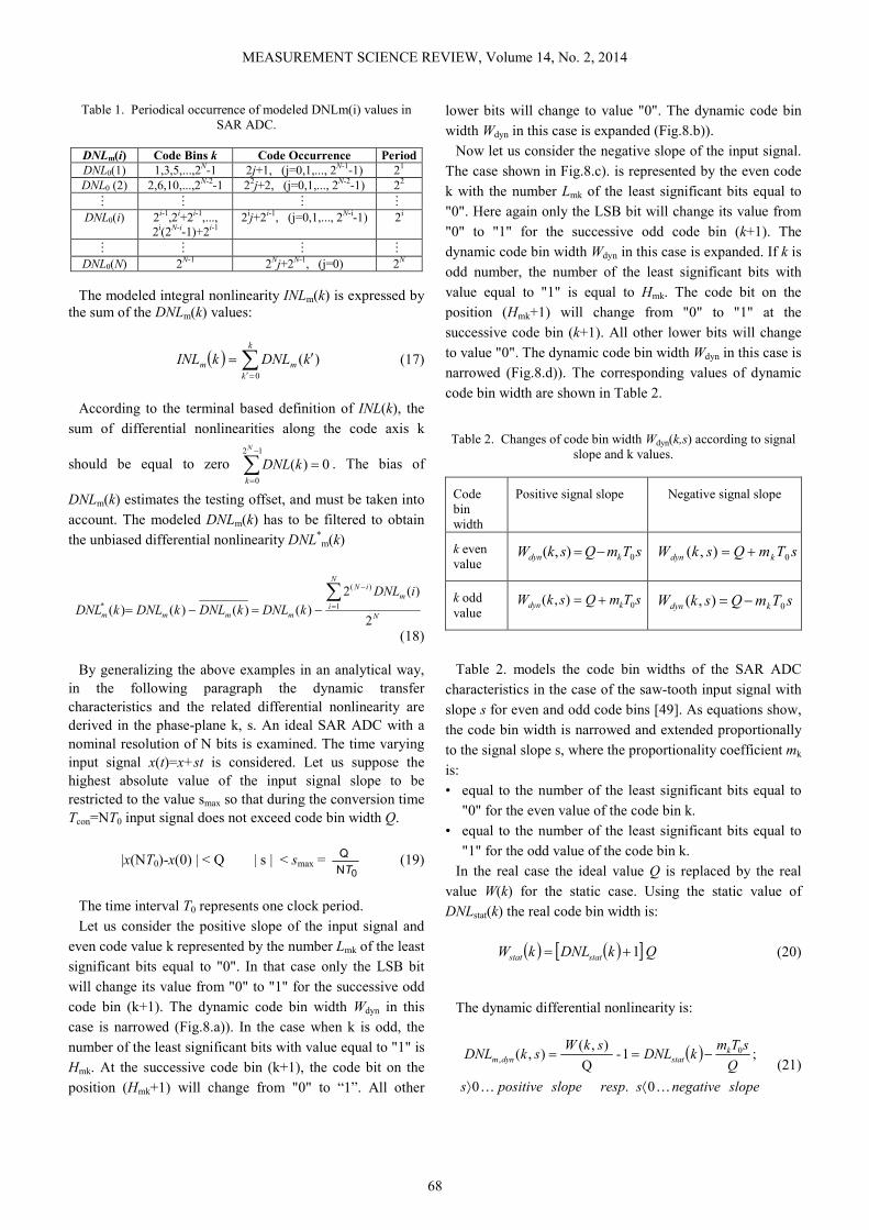
Table 1. Periodical occurrence of modeled DNLm(i) values in SAR ADC.
DNLm(i) Code Bins k Code Occurrence Period
DNL0(1) 1,3,5,...,2N-1 2j+1, (j=0,1,..., 2N-1-1) 21 DNL0 (2) 2,6,10,...,2N-2-1 22
j+2, (j=0,1,..., 2N-2-1) 22 M M M M
DNL0(i) 2i-1,2i+2i-1,..., 2i(2N-i-1)+2i-1
2ij+2i-1, (j=0,1,..., 2N-i-1) 2i
M M M M DNL0(N) 2N-1 2N
j+2N-1, (j=0) 2N
The modeled integral nonlinearity INLm(k) is expressed by the sum of the DNLm(k) values:
( ) ∑=′
′=k
k
mm kDNLkINL0
)( (17)
According to the terminal based definition of INL(k), the
sum of differential nonlinearities along the code axis k
should be equal to zero 0)(12
0
=∑−
=
N
k
kDNL . The bias of
DNLm(k) estimates the testing offset, and must be taken into
account. The modeled DNLm(k) has to be filtered to obtain
the unbiased differential nonlinearity DNL*
m(k)
N
N
i
m
iN
mmmm
iDNL
kDNLkDNLkDNLkDNL2
)(2
)()()()( 1
)(
*∑
=
−
−=−=
(18)
By generalizing the above examples in an analytical way, in the following paragraph the dynamic transfer characteristics and the related differential nonlinearity are derived in the phase-plane k, s. An ideal SAR ADC with a nominal resolution of N bits is examined. The time varying input signal x(t)=x+st is considered. Let us suppose the highest absolute value of the input signal slope to be restricted to the value smax so that during the conversion time Tcon=NT0 input signal does not exceed code bin width Q.
|x(NT0)-x(0) | < Q | s | < smax = 0N
Q
T (19)
The time interval T0 represents one clock period.
Let us consider the positive slope of the input signal and
even code value k represented by the number Lmk of the least
significant bits equal to "0". In that case only the LSB bit
will change its value from "0" to "1" for the successive odd
code bin (k+1). The dynamic code bin width Wdyn in this
case is narrowed (Fig.8.a)). In the case when k is odd, the
number of the least significant bits with value equal to "1" is
Hmk. At the successive code bin (k+1), the code bit on the
position (Hmk+1) will change from "0" to “1”. All other
lower bits will change to value "0". The dynamic code bin
width Wdyn in this case is expanded (Fig.8.b)).
Now let us consider the negative slope of the input signal.
The case shown in Fig.8.c). is represented by the even code
k with the number Lmk of the least significant bits equal to
"0". Here again only the LSB bit will change its value from
"0" to "1" for the successive odd code bin (k+1). The
dynamic code bin width Wdyn in this case is expanded. If k is
odd number, the number of the least significant bits with
value equal to "1" is equal to Hmk. The code bit on the
position (Hmk+1) will change from "0" to "1" at the
successive code bin (k+1). All other lower bits will change
to value "0". The dynamic code bin width Wdyn in this case is
narrowed (Fig.8.d)). The corresponding values of dynamic
code bin width are shown in Table 2.
Table 2. Changes of code bin width Wdyn(k,s) according to signal slope and k values.
Code bin width
Positive signal slope Negative signal slope
k even value
sTmQskW kdyn 0),( −=
sTmQskW kdyn 0),( +=
k odd value
sTmQskW kdyn 0),( +=
sTmQskW kdyn 0),( −=
Table 2. models the code bin widths of the SAR ADC
characteristics in the case of the saw-tooth input signal with
slope s for even and odd code bins [49]. As equations show,
the code bin width is narrowed and extended proportionally
to the signal slope s, where the proportionality coefficient mk
is:
• equal to the number of the least significant bits equal to
"0" for the even value of the code bin k.
• equal to the number of the least significant bits equal to
"1" for the odd value of the code bin k.
In the real case the ideal value Q is replaced by the real
value W(k) for the static case. Using the static value of
DNLstat(k) the real code bin width is:
( ) ( )[ ] QkDNLkW statstat 1+= (20)
The dynamic differential nonlinearity is:
( )
slopenegativesrespslopepositives
Q
sTmkDNL
skWskDNL k
statdynm
KK 0.0
;1 - Q
),( ),( 0
,
⟨⟩
−== (21)

MEASUREMENT SCIENCE REVIEW, Volume 14, No. 2, 2014
69
t
T(k+1)
Tdyn(k+1)
T(k)
Tdyn(k)
s
1T0 2 T0 3 T0 4 T0 5 T0 6 T0
k=1,0,1,0,0,0 CD
0
e
Q Wdyn
x(t)=Tdyn(k)+s.t
k+1=1,0,1,0,0,1
a.)
t
e T(k+1)
Tdyn(k+1)
T(k)
x0=Tdyn(k)
Q
1Τ0 2Τ0 3Τ0 4Τ0 5Τ0 6Τ0
k= 1,0,0,1,1,1
0
Wdyn s k+1= 1,0,1,0,0,0
x(t)=Tdyn(k)+s.t
b.)
t
T(k+1)
Tdyn(k+1)
T(k)
Tdyn(k)
s
1T0 2 T0 3 T0 4 T0 5 T0 6 T0
k=1,0,1,0,0,0
CD
0
e
Q Wdyn
x(t)=Tdyn(k)-s.t
k+1=1,0,1,0,0,1
c.)
t
T(k+1) Tdyn(k+1)
T(k)
Tdyn(k) Q
1Τ0 2Τ0 3Τ0 4Τ0 5Τ0 6Τ0
k= 1,0,0,1,1,1
0
Wdyn
s
k+1= 1,0,1,0,0,0
x(t)=Tdyn(k)-s.t
d.)
Fig.8. Influence of signal slope on the code bin width for SAR ADC.
The equation (21) represents the ADC analytical model of
the dynamic DNLm,dyn(k,s). Consequently, also the dynamic differential nonlinearity trend in the two dimensional domain of slope s and code k is related to the code composition. DNLm,dyn(k,s) is represented for even codes k by the extension of the static one by the product of signal slope and number mk of the least code bits with the value equal to "0". In contrary to the odd codes k, the static differential nonlinearity is extended by the product of slope s and number mk of the least bits with the value equal to "1". The proportionality coefficient for all those examples is T0/Q. The acquired DNLdyn(k,s) characteristic for 12 bit SAR
ADC Maxim574AJN in the phase plain (k,s) is shown in Fig.10. Measured characteristic is similar to the simulated function DNLm,dyn(k,s) (21) under the assumption of DNLstat(k)=0 for the same values (k,s).
B. Experimental verification.
The structural model of SAR ADC was experimentally verified in [18]. The validation example of the multiperiodical INL(k) occurrence is shown for an actual 12 bit ADC implemented on the ATMEL ADuC 812 microcontroller in the bipolar mode (Fig.9.). The modeled values of differential nonlinearities DNLm(k) were obtained by the averaging of measured values of DNL from the histogram test. The code bins were chosen according to the periodical model (Table 2.). Only three dominant differential nonlinearities were taken for the model. The crucial nonlinearities are typical for the structural ADC model and they were taken in the middle of FSR (DNL0(N)), quarters of FSR (DNL0(N-1)) and eights of FSR (DNL0(N-2)). The periodical error effects connected with bits of lower significance are hidden in the superimposed random effects caused by error sources not involved in the structural model and by the testing uncertainty.
Different shape of the nonlinearity model for the other sample of 12 bit SAR DAC in unipolar mode (LAB-PC-1200 by NI) is shown in Fig.14. Presented experimental results show the practical objective of the error model presented in the previous part. Although the shapes of the integral nonlinearities are different inherent to the particular ADC chip, their periodical character remains the same. Moreover, the experimental results allow to select code bins with significantly large DNLm(k). Differential nonlinearities can be measured by the fast testing procedure based on the testing signal with reduced amplitude [4], [12], [13].
Fig.9. INL(k) characteristics acquired from 12 bit ADC implemented on ATMEL ADuC 812 microcontroller and a.) modeled by Rademacher function (16).
Simulation and experimental tests of differential nonlinearities under dynamic conditions were carried out on an actual 12 bit SAR ADC Maxim MX574AJN with full scale ±5.0 V, and the maximum conversion time 25 µs. Firstly, the average quantization step Q equal to 2.44 mV was obtained from standardized test results using terminal definition. The differential dynamic nonlinearity was measured by the histogram test with the saw-tooth stimulus signal with peak-to-peak voltage 10.5 V [27]. Testing slope values were set in the equidistant steps 0.2.smax within interval (-smax,+smax). Approximately 82,106 samples were acquired for each slope value. The experimental results are shown in Fig.10. The performed tests show that with increasing slope of input signal, the differential nonlinearity increases, too. Experimental results of DNL(k,s) of SAR ADC match well with the modeled DNLm(k,s).

MEASUREMENT SCIENCE REVIEW, Volume 14, No. 2, 2014
70
Fig.10. Experimentally acquired characteristic of DNLdyn(k,s) in the phase plane (k,s) for 12 bit SAR ADC Maxim MX574AJN.
3.3. THE CYCLIC ADC
Cyclic (algorithmic) ADCs represent architecture, where the output value is achieved by several cycles of flash conversion with the increasing resolution from coarse to fine digital values [16], [21]. Let us consider N-bit ADC operating in L cycles. In the first cycle the input voltage x is
coarsely converted into 2N
/L levels. The binary output value 1k is memorized in the output register and converted by
DAC in its analog equivalent. The difference between analog voltage at the ADC input and recovered voltage from DAC output is subtracted, registered in sample and hold
circuit and amplified by 2N
/L. The output signal from the
amplifier is connected to the ADC in the successive cycle through the input switch and converted into value 2
k. Similarly to the previous tact, DAC in the feedback generates analog equivalent of 2
k, which is successively subtracted and memorized in sample and hold circuit (S&H). The output signal from S&H circuit is amplified by 2N
/L for the next cycle by amplifier (A). Working procedure
is characterized by the refining of the estimation of digital equivalent of the input voltage in each conversion cycle.
Code segments lk of length N/L from the most significant bit
positions to the least significant are memorized in the digital output register.
The number of conversion cycles L depends on the architecture variants. In the extreme case, the number of cycles L is equal to the number of bits N. This variant is suitable for ADCs using switched capacitor technology where a potential high operating frequency allows using simple comparators as the binary ADC. One bit DA conversion is performed by connecting the output node either to the ground or reference voltage according to the input bit ki. The great advantage of the switched capacitor technology is the possibility to implement the autozeroing procedure, which efficiently suppresses offset and gain errors of the analog blocks in the ADC structure.
A. Generalized cyclic ADC.
Let us consider a generalized cyclic ADC from Fig.11. with the resolution of the flash ADC and DAC in the
feedback equal to 2N
/L and unipolar input voltage
xADC∈⟨0,FSR⟩. The number of the code bits lk in the l-th
cycle is N/L. The estimation of code segment of output code (l+1)
k in (l+1)-th cycle is performed by the rounding operation of the amplified difference between ADC input voltage from the previous l-th cycle and voltage recovered using code window l
k. The rounding operation corresponds mathematically to AD conversion. The overall nonlinearity in the direct branch INLADC(k) consists of switch error and nonlinearity of flash ADC. The integral nonlinearity INLDAC(k) of the converting DAC causes an additional error of subtraction of both voltages in the feedback branch. S&H circuit together with the amplifier A are characterized by the resulting offset UOFF and gain error δ. Those errors are included into the nonlinearity INLDAC(k) of the DAC in the feedback.
Fig.11. Structural model of cyclic ADC.
The code segment 1k obtained from the ADC output in
direct branch for xADC is:
DACDAC
ADC
ADC QkUQ
xk .; 11 =
= (22)
Angular brackets represent rounding operation as
mathematical description of analog to digital conversion. The quantization steps Q of ADC and DAC in the ideal case are
QFSR
QQL
NDACADC ===2
(23)
In the first cycle the integral nonlinearity is determined by
( ) ( )kINLLkINL ADC
11 ...1, = (24)
In the second cycle the input voltage xIN of ADC is
( )( ) ( )
( )( ) ( )δUQkINLxx
δUQkINLkQxx
LN
OFFDACIN
Id
IN
LN
OFFDACADCIN
+−−=⇒
++−−=
12
12
1
11
(25)
SW
ITC
H
Flash ADC
2N/L
S&H circuit
Output
register
x xIN
k
A=2N/L(1+δ)
DAC
2N/L
QDAC= QADC=
=FSR/2N/L
UOFF

MEASUREMENT SCIENCE REVIEW, Volume 14, No. 2, 2014
71
here idxIN represents ideally amplified difference voltage
from subtracting circuit ready for conversion in the second cycle. The difference between the real quantization levels of ADC and DAC is included in the INLDAC(k).
The code segment 2k is obtained in the second conversion
cycle. The error voltage e on ADC input is:
( ) ( )( ) ( )δUQkINLQkINLe LN
OFFDACADC +−−= 1212
(26) The ADC input voltage in the third conversion cycle is
( ) ( ) ( )δδUQkINLxx LN
LN
OFFDACIN
id
IN +
+−−= 12122
(27)
Where the input voltage idxIN for the ideal case is:
( ) LN
LN
IN
Id kQkQxx 22 21
−−= (28)
The total error voltage e on the ADC input in the third
cycle is:
( ) ( ) ( ) ( )
( ) ( ) ( ) ( )2
23
23
1212
1212
+++′−′=
=+
+−′−′=
δUδQkINLQkINL
δδUQkINLQkINLe
LN
OFFL
N
DACADC
LN
LN
OFFDACADC (29)
The ADC input voltage in the l-th conversion cycle is:
( ) ( )δδUQkINLxx LN
l
LN
OFFl
DACINid
IN +
+−′
−=
−− 1212
21 (30)
In addition to the ideal input voltage id
xIN the second part represents input error voltage.
Integral nonlinearity of the whole cyclic ADC is:
( )( ) ( ) ( ) ( )
Q
δUδQkINLQkINL
kkkINL
l
LN
OFFL
Nl
DAC
l
ADC
l
′
+++−
=
=−
−1
1
21
1212
)31(,..,
The resulting quantization step is LLN
NQ
FSRQ
)1(
22
−
==′ .
It allows simplifying the formula of the final modeled integral nonlinearity for low gain error of the S&H with the amplifier A.
( ) ( ) ( ) ( )
( ) ( )3221
122,..,
)1(1
1)1(
21
LlLN
OFFl
LN
l
DAC
l
ADCL
LNl
FSR
Uδ
δkINLkINLkkkINL
−+−
−−
++
+
+−≅
Taking into account δ⟨⟨1 the expression (32) could be
simplified
( ) ( ) ( )
( )( ) ( )33211
22,..,
)1(
1)1(
21
LlLN
OFF
LN
l
DAC
l
ADCL
LNl
FSR
Uδl
kINLkINLkkkINL
−+
−−
−++
+
−≅
The formula (33) shows the basic pattern of the error
function INL(k) of a cyclic ADC. It is based on repetition of
the segment of the INL with the length 2N
/L over the FSR.
Shape of this segment depends on the N/L low significant
bits of the output digital value. By increasing the number of the conversion cycles the number of the repetitions of the basic error segment of the INL(k) is increasing.
B. Experimental verification
INL(k) of the cyclic ADC was measured in [16]. Experimental results show conformity with the structural model covering the dominant error sources. The tested 12-bit cyclic ADC was AD 9430 operating up to a 210 MSPS and optimized for extreme dynamic performance in broadband systems (Fig.12.). The final conversion result is achieved after four cycles using 3-bit flash ADC. Measured INL(k) shows repetition of 16=24 similar segments with the length of 8=23 codes. Each segment is bordered by the local peaks in the INL(k) function. The deviations of the smoothed INL shape at both ends of FSR are caused by the error sources not involved in the error model (33). Table 3. shows prevalent characteristics of structural error models.
Fig.12. INL(k) of 12-bit cyclic ADC (AD9430).
Table 3. Prevalent functional characteristic of the structural error
models for basic ADC architectures. Architecture Prevalent functional
characteristic
Full-Flash ADCs (one step conversion cycle)
Random function
Integrating ADCs, (one, dual slope), Σ∆ ADCs, Voltage to Frequency Converters
Polynomial function
N-bit Successive approximation ADCs
Rademacher function with N code frequencies
Pipeline ADCs, Cyclic Flash ADCs, with L-cycles
Periodical function with L code frequencies.
MEASUREMENT SCIENCE REVIEW, Volume 14, No. 2, 2014
72
4. BEHAVIORAL ERROR MODELS
Parallel (Flash) ADC is an example of the principle where each code level is determined by different component. The error sources in the ADC structure are not apparent with the regular causalities in the error functions. In other cases, when the information about internal architecture of the utilized ADC is missing, a more suitable way of the error modeling is utilization of the behavioral error model [14], [23], [30]. Moreover, the regularly demonstrated error sources are suppressed by the permanent progress in microelectronics. The errors caused by EMC interferences and improper operational conditions become prevalent and are demonstrated without any regular relation. The universal method for the error modeling in this case is the generic ADC error model represented by the black boxes. Input of these boxes are code levels k and output are the values of INL(k) or DNL(k) described by the mathematical formulae that match better with measured results, or by the memorized values.
4.1. LOOK UP TABLE ERROR MODELS
The simplest way how to model functional errors of an ADC is the look up table with the memorized integral nonlinearities of ADC. In general, the input of the tables are codes k or/and slope s of digital signal. In the case of ADC error models the look up table block is in the feedback. This model represents the simplest generic behavioral error model [21]. The main disadvantage of this model is low reduction of information about the error function INL(k) or DNL(k). The absence of information on regular dependencies in the error model does not allow utilizing the modeling advantages described in the introduction. It is just another form of presentation of the testing results. Examples of such models are shown in Fig.15.
4.2. UNIFIED ERROR MODEL
Previously analyzed error models showed the relation between the ADC structures and their mathematical description. Two basic types of the ADC nonlinearities were obtained for the studied structural error models. The integral nonlinearity caused by ADCs with intermediate transformation of the input signal x in the selected analog parameter in APS and quantization in QS (Fig.2.) could be modeled by a polynomial function (7) of the code bin k with the order P. On the other hand, the error function INL(k) with discontinuities is typical for the ADCs using the feedback compensation of the input signal x by the DAC controlled by the various algorithms. The nonlinearity of some ADC representatives is described by the formula (16) for SAR ADC and formula (33) for cyclic ADC, respectively. The progress in the ADC technology is aimed at suppression of error sources causing the discontinuities in the INL(k) function. The influence of the analog preprocessing blocks becomes dominant because of the limited possibility to reduce parasitic influence of temperature and operational conditions on the analog circuits.
Because of this fact, the optimal way how to describe both parts of any ADC model is the unified error model expressed as one dimensional image in the code k domain consisting of two components [18], [49]. a. The low code frequency component (LCF), which is
represented by the polynomial approximation LCF
INLm(k) of P-th order. The approximation of the polynomial function is obtained from the measured INL(k) values in the L nodal points k∈<k1, k2,.., kL>. The most suitable approximation uses the Least Squared approximation.
b. The high code frequency component (HCF) HCFINLm(k)
caused by significant deviations from the mean value of the differential nonlinearities DNLm(k). The code bins with significantly different nonlinearities have both the regular occurrence of the modeled values of DNLm(k), and a random appearance. The periodical occurrence of various types of DNL according to the Rademacher function in SAR ADC (16) or periodical repetition of two nonlinear functions (33) for cyclic ADC is the most frequent situation. The progress in the ADC technology suppressed the main regularity in the DNL(k) behavior. The HCF component is able to cover nonlinearities out of the regular occurrence. Characteristic values of DNLm(i) for the periodic model are estimated using a narrow band histogram for the binary codes ki where at the bit position i is changing from "0" to "1", for increment of k.
The modeled shape of the integral nonlinearity using both components is as follows:
( ) ( ) ( ) ( ) ( )∑=
+=+=k
i
m
HCF
m
LCF
m
HCF
m
LCF
m kDNLkINLkINLkINLkINL0
(34)
While the component LCF
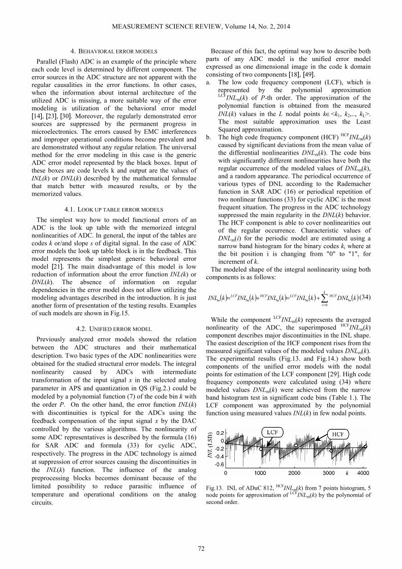
INLm(k) represents the averaged nonlinearity of the ADC, the superimposed HCF
INLm(k) component describes major discontinuities in the INL shape. The easiest description of the HCF component rises from the measured significant values of the modeled values DNLm(k). The experimental results (Fig.13. and Fig.14.) show both components of the unified error models with the nodal points for estimation of the LCF component [29]. High code frequency components were calculated using (34) where modeled values DNLm(k) were achieved from the narrow band histogram test in significant code bins (Table 1.). The LCF component was approximated by the polynomial function using measured values INL(k) in few nodal points.
Fig.13. INL of ADuC 812, HCFINLm(k) from 7 points histogram, 5 node points for approximation of LCFINLm(k) by the polynomial of second order.

MEASUREMENT SCIENCE REVIEW, Volume 14, No. 2, 2014
73
Ideal ADC
2N
x(iTS)
∆x
k(iTS)
∆t=TS
s LCFINL(k,s)
k
s HCFINL(k,s)
k
IdealDAC
Σ
Σ
IdealDAC
Fig.14. Modeled INLm(k) of LAB-PC-1200 where HCFINLm(k) is determined by narrow band histogram in 7 points, and LCFINLm(k) approximated by third order polynomial from 9 nodes.
The measuring chain consists usually of a sensor of
measured physical quantity and Data Acquisition Board. Here the input quantity is represented by the measured analog physical quantity and the output values are digital time samples. The transfer function has similar step-like form as any ADC. Dominant error effects are involved by the analog processing part - mainly sensors. Because of this reason the LCF component LCF
INLm(k) in the unified error model is dominant. The ADC data sheet comparison shows continual improvement of metrological parameters caused by the progress in electronic technology. Improper ADC implementation and unstable working conditions become dominant error contributors with the continuous LCF characteristic.
The authors in [17], [49] showed that the unified error model can be generalized even with its dynamic component (Fig.15.). The signal slope s(iT0) is calculated from the data flow. For the actual value of code k(iT0) and slope s(iT0), low and high code frequencies are taken from the look up table. According to the INL(k,s) definition [1], [2] both nonlinearity components are subtracted from the analog input of an ideal ADC. The implementation of the unified dynamic model considers limited signal variation (x(t)-x(t-TS) << Q.
Fig.15. Unified ADC dynamic model.
4.3. BEHAVIORAL ERROR MODELS DESCRIBED BY
ANALYTICAL FORMS
The possibility to implement Chebyshev’s series for ADC modeling was studied in [7], [8]. The proposed model has a concise mathematical form with the sum of Chebyshev’s functions covering all details in the ADC characteristics. Let us consider the results of FFT testing by the harmonic stimulus signal ( ) CωiTViTx SS += )cos( . If a purely static
model of the systematic error is assumed, the output signal is determined by
( ) ( ) ( ) ( )SSS
S iTeQ
CωiTVINL
Q
CωiTViTk +
++
+≅
coscos (35)
The output may be represented as a series of in-phase
cosine harmonics caused by the nonlinearity of the transfer characteristics. The error component e(iTs) is transformed in a spectral domain E(nω) and it takes into account all the random errors. The error component E(nω) as the spectral noise floor could be suppressed by the FFT calculation using the averaged output record for the same harmonic stimulus signal. The output signal impacted by the systematic contribution of ADC nonlinearities is
( ) ( ),
2 1
0 ∑∞
=
−+≅
n
SnnS
V
CiTxCa
aiTk (36)
where Cn(ζ) represents the first kind Chebyshev polynomials of the order n.
( ) ( )( )ζnζC n arccos.cos= (37)
Obviously, if one wants the model given by (36) to be
appropriate to describe the behavior of a real ADC, the test must be performed at a sufficiently low frequency ω. The signal at the ADC output with a high resolution includes the effect of integral nonlinearity. The final value of the INL(k) is obtained by the subtraction of the distorted output signal from the ideal one.
( ) ( ) ( );1
1∑∞
=
−=n
nn kCQ
VkCakINL (38)
The authors of the article [8] proposed the implementation
of spectral analysis even for the estimation of the hysteresis error as dynamic superimposed signal h(k) to the distorted one.
a.) b.)
Fig.16. Comparison between the measured INL(k) (thin line) and the modeled INLm(k) obtained by a 100-harmonic a) and by 30-harmonic b) Chebyshev test (thick line). The harmonics were obtained from harmonic tests of 8-bit Flash ADC using incoherently sampled sine wave.
Another model proposed in [6] considers the
approximation of INL(k) by the series of harmonic functions associated with code k. The fundamental code frequency of
ADC nonlinearity is Ω=2π/2N. The details in INL(k) shape

MEASUREMENT SCIENCE REVIEW, Volume 14, No. 2, 2014
74
are described by the multiples mΩ=m2π/2N of the
fundamental code frequency. The integral nonlinearity INL(k) is determined by the Fourier series in the code domain
( ) ( )( );sincos2
)(max
1
0 ∑=
Ω+Ω+≈M
m
mm kmbkmaa
kINL (39)
The number of code harmonics in the model is restricted to
Mmax. The stimulus signal is represented by the ideal harmonic
function x(iTS) with the frequency f0 sampled by the frequency fs.
if
fπiTe
FSR
ViTx
S
iSiS00 2);(cos)( =Θ+Θ= (40)
Let us consider the ratio
MJ
ff
S
=0 where J and M are
relatively prime numbers. Under these circumstances the calculated frequency spectrum will be without leakage error. For M>J22N quantization error is lower than code bin width Q and all codes k(iTS) occur in the recorded ADC output signal. The quantization noise e(iTS) is negligible. All harmonic components in the output spectra for harmonic stimulus will be a product of nonlinear distortion caused by INL(k). Under this consideration the output signal k(iTS) is expressed by the series of harmonics in the time domain
( )( ) ( )
( ) ( )∑
∑
∑=
=++
=
−=
−==Θ+=
max
max
max
0
11212
122
)12
12;cos
)()(
L
l
M
m
lm
l
l
M
m
lm
l
l
lilS
S
αmJbS
αmJaS
SlSQ
iTxiTk
(41)
where Sl represents the amplitude of the l-th harmonic, and the constant. Function Jn(α) in the expression for Sl is the Bessel function of the first kind with order n.
Let us consider the number of the FFT harmonics in the spectral domain to be Lmax for the signal k(iTS). The maximal number of the harmonics describing INL(k) in the code frequency domain is Mmax Due to dimension matching the optimal relation between values Lmax and Mmax is Lmax=2Mmax. As a consequence, the relation between the amplitudes Sl of the l-th harmonic of the testing signal k(iTS)
and Fourier expansion of the INL(k) in the code domain (a0,..aMmax, b0,..bMmax) is estimated by means of the matrix product.
( ) ( ) )42(;0;;0;where
......0
:::::::
......0
......21
;
:
:
:
1212
12122
2
11
11
111
1
01
001
0
0
0
0
max
maxmax
max
maxmax
maxmax
maxmax
max
max
max
max
====
=
=
++
++
==
===
=
m
l
lm
l
m
l
lm
l
M
LL
M
LL
MM
M
l
m
l
M
l
m
l
M
M
L
L
BαkJBAαkJA
BAAA
BAAA
BAAA
b
b
a
a
S
S
A
A
AA
A
A
TT
The harmonic components S0,S1,..SLmax are calculated from the registered ADC output flow k(iTS) for sine wave stimulus by FFT without leakage. The modeled INL(k) can be estimated by the inverse matrix relation
;:
:
:
max
max
max
max
01
0
0
=
−
L
L
M
M
S
S
b
b
a
a
T (43)
Fig.17. Measured and modeled INL(k) of 12-bit ADC TDA 8769 using transformation of the FFT spectrum [7]. The maximal number of code frequency components is Mmax=100 calculated from Lmax=200 spectral components.
Integral nonlinearity calculated by this method is
implemented in the look up table block (Fig.15.) where just one type of INL(k) is memorized. Model description by a mathematically concise formula is the main advantage of the last two models. The disadvantage is a high number of harmonics, which have to be taken into account. On the contrary, the unified model with few parameters has the highest redundancy for INL(k) description. It requires a few polynomial coefficients for LCF
INL(k) and a few significant DNL(k) values for the description of HCF
INL(k).
5. CONCLUSIONS
The performed study shows that the ADC hardware structure determines continuous or periodic shape of the nonlinearity function. Continuous INL(k) shape is typical for ADCs, where input signal is converted to frequency or time using various circuits. Periodical nonlinearity related to particular code bins of the output binary code is typical for SAR ADC; while periodical repetition of the similar nonlinearity segment over the FSR is typical for cyclic ADC. Another type of the periodic regularity of error function represents cyclic ADCs.
The limits of the structural models are given by the various reasons. The first limitation occurs when the modeled internal structure of the ADC does not have key circuit block with dominant error. Parallel ADCs are an example where each code level is determined by a different component. The second limitation is caused by the progress in technology where the dominant error sources are getting better suppressed. It restricts influence of the dominant

MEASUREMENT SCIENCE REVIEW, Volume 14, No. 2, 2014
75
structural blocks on the final error function. Prevailing error sources are becoming errors caused by the charge injection, galvanic coupling, etc. Their final error function depends on the ADC chip and printed board layout. Moreover, glitches of various sources have weak regularity.
The behavioral error model allows to describe main ADC and DAC imperfections by the generic structure with the values of systematic errors like INL(k) and DNL(k). ADC nonlinearities are initial information for the estimation of other systematic error parameters like THD, offset and gain errors. The description of the converter error functions by their error models neglects redundant information and the error models highlight the peculiar error sources in the structural models or on the main nonlinearity pattern characteristics by behavioral error models. Various techniques for the patter recognitions could be utilized for the simplification of error models. Error pattern parameters are constants memorized in the black boxes. The unified error models describe nonlinearity functions as a one-dimensional image which consists of the sum of a smoothed sub-image described by the low code frequencies and a wave component described by the high code frequency. While the first one describes errors of the continuous signal processing in the conversion procedure, the second one describes periodical manifestation of the weighting component mismatch. The structural model of the converter facilitates the choice of the optimal function for description of both components. À-posteriori transformation of testing results with the suitable mathematical method allows recovering the redundant error parameters together with mathematical formula, which corresponds to the used behavioral error model.
ACKNOWLEDGMENTS
The work is a part of the project supported by the Science Grant Agency of the Slovak Republic (No. 1/0281/14) and Educational Grant Agency of Slovak republic (No. 029TUKE-4/2012).
REFERENCES
[1] IEEE Std. (2008). IEEE Standard for digitizing
waveform recorders. 1057-2007. New York: IEEE. [2] IEEE Std. (2011). IEEE Standard for terminology and
test methods for analog-to-digital converters. 1241-2010. New York: IEEE.
[3] Arpaia, P., Daponte, P., Michaeli, L. (1999). The influence of the architecture on ADC modelling. IEEE
Transactions on Instrumentation and Measurement, 48 (5), 956-967.
[4] Alegria, F., Arpaia, P., Daponte, P., Serra, A.C. (2002). An ADC histogram test based on small-amplitude waves. Measurement, 31 (4), 219-279.
[5] Vargha, B., Shoukens, J., Rolain, Y. (2001). Non-linear model based calibration of A/D converters. In 6th Euro Workshop on ADC Modelling and Testing, 13-14 Sept. 2001, Lisbon, Portugal, 79-83.
[6] Janik, J.M. (2003). Estimation of A/D converter nonlinearities from complex spectrum. In 8th
International Workshop on ADC Modelling and
Testing, 8-10 Sept. 2003, Perugia, Italy, 205-208.
[7] Adamo, F., Attavissimo, F., Giasquinto, N. (2000). Measurement of ADC integral nonlinearity via DFT. In 5th International Workshop on ADC Modelling and
Testing, 26-28 Sept. 2000, Vienna, Austria, 3-8. [8] Adamo, F., Attivissimo, F., Giaquinto, N., Kale, I.
(2007). Frequency domain analysis for dynamic nonlinearity measurement in A/D converters. IEEE
Transactions on Instrumentation and Measurement, 56 (3), 760-768.
[9] Attivissimo, F., Giaquinto, N., Kale, I. (2004). INL reconstruction of A/D converters via parametric spectral estimation. IEEE Transactions on
Instrumentation and Measurement, 53 (4), 940-946. [10] Arpaia, P., Daponte, P., Rapuano, S. (2004). A state of
the art on ADC modelling. Computer Standards &
Interfaces, 26 (1), 31-42. [11] Chen, T., Gielen, G. (2003). Analysis of the dynamic
SFDR property of high-accuracy current-steering D/A converters. In International Symposium on Circuits
and Systems, 25-28 May 2003, Bangkok, Thailand. IEEE, Vol. 1, 973-976.
[12] Vargha, B., Schoukens, J., Rolain, Y. (2002). Using reduced-order models in D/A converter testing. In 19th Instrumentation and Measurement Technology
Conference, Anchorage, USA. IEEE, Vol. 1, 701-706. [13] Hassan, I.H.S., Arabi, K., Kaminska, B. (1998).
Testing digital to analog converters based on oscillation-test strategy using sigma-delta modulation. In International Conference on Computer Design -
VLSI in Computers and Processors, 5-7 Oct. 1998, Austin, Texas. IEEE, 40-46.
[14] Arpaia, P., Cennamo, F., Daponte, P., D´Apuzzo, M. (1996). A behavioural model for scan converter based transient digitizers. Measurement, 17 (2), 103-114.
[15] Björsell, N., Händel, P. (2006). Dynamic behavior models of analog to digital converters aimed for post-correction in wideband applications. In IMEKO World
Congress : 11th Workshop on ADC Modelling and
Testing, 17-22 Sept. 2006, Rio de Janeiro, Brazil. [16] Medawar, S., Händel, P., Bjorsell, N., Jansson, M.
(2010). Input dependent integral nonlinearity modeling for pipelined analog-digital converters. IEEE
Transactions on Instrumentation and Measurement, 59 (10), 2609-2620.
[17] Medawar, S., Händel, P., Björsell, N., Jansson, M. (2008). ADC characterization by dynamic integral non-linearity. In 13th Workshop on ADC Modeling
and Testing, 22-24 Sept. 2008, Florence, Italy, 1-6. [18] Michaeli, L., Michalko, P., Saliga, J. (2008). Unified
ADC nonlinearity error model for SAR ADC. Measurement, 41 (2), 198-204.
[19] Arpaia, P., Daponte, P., Michaeli, L. (1999). A dynamic error model for integrating analog-to-digital converters. Measurement, 25, 255-264.
[20] Medawar, S., Handel, P., Björsell, N., Jansson, M. (2011). Postcorrection of pipelined analog digital converters based on input-dependent integral nonlinearity modeling. IEEE Transactions on
Instrumentation and Measurement, 60 (10), 3342-3350.

MEASUREMENT SCIENCE REVIEW, Volume 14, No. 2, 2014
76
[21] Lundin, H., Händel, P. (2014). Look-up tables, dithering and volterra series for ADC improvements. In Design, Modeling and Testing of Data Converters. Springer, 249-275.
[22] Nikaeen, P. (2008). Digital compensation of dynamic
acquisition errors at the front-end of ADCs. Dissertation, Stanford University, Stanford, CA, USA.
[23] Brigati, S., Liberali, V., Maloberti, F. (1994). Precision behavioural modelling of circuit components for data converters. In Second International
Conference on Advanced A-D and D-A Conversion
Techniques and their Applications, 6-8 July 1994. IEEE, 110-115.
[24] Balestrieri, E., Daponte, P., Rapuano, S. (2004). A state of the art on ADC error compensation methods. In 21st Instrumentation and Measurement Technology
Conference, 18-20 May 2004. IEEE, Vol. 1, 711-716. [25] Ruan, G. (1991). A behavioral model of A/D
converters using a mixed-mode simulator. In IEEE
Transactions on Solid-State Circuits, 26 (3), 283-290. [26] Vargha, B., Zoltan, I. (2001). Calibration algorithm for
current – output R-2R ladders. IEEE Transactions on
Instrumentation and Measurement, 50 (5), 1216-1220. [27] Arpaia, P., Daponte, P., Michaeli, L. (1998).
Analytical a priori approach to phase-plane modeling of SAR A/D converters. IEEE Transactions on
Instrumentation and Measurement, 47 (4), 849-857. [28] Mirri, D., Iuculano, G., Filicori, F., Pasini, G.,
Vannini, G. (1995). Modeling of non ideal dynamic characteristics in S/H-ADC devices. In Instrumentation and Measurement Technology
Conference, 24-26 April 1995. IEEE, 27. [29] Michaeli, L., Šaliga, J., Michalko, P. (2007).
Triangular testing signal for identification of unified error model parameters. Measurement, 40 (5), 491-499.
[30] Hejn, K. (1998). A behavioral model of fast AD converter. In IMEKO TC-4 : 1st International
Workshop on ADC Modelling. Smolenice, Slovakia, 28-38.
[31] Maloberti, F. (2007). Data Converters. Springer. [32] Seckin, U., Ken Yang, C. (2008). A comprehensive
delay model for CMOS CML circuits. IEEE
Transactions on Circuits Systems I: Regular Papers, 55 (9), 2608-2318.
[33] Jerng, A., Sodini, C.G. (2007). A wideband ∆Σ digital-RF modulator for high data rate transmitters. IEEE
Journal of Solid-State Circuits, 42 (8), 1710-1722. [34] Agrež, D. (2011). Quantization noise of the non-
uniform exponential tracking A/D conversion. In 16th
IMEKO TC4 : 2011 International Workshop on ADC
Modelling, Testing and Data Converter Analysis and
Design and IEEE 2011 ADC Forum, Orvieto, Italy. [35] Van de Plassche, R. (2010). CMOS Integrated Analog-
to-Digital and Digital-to-Analog Converters. Springer.
[36] Haenzsche, S., Henker, S., Schuffny, R. (2010). Modelling of capacitor mismatch and non-linearity effects in charge redistribution ADCs. In Mixed
Design of Integrated Circuits and Systems : 17th
International Conference, 24-26 June 2010. IEEE, 300-305.
[37] Mashhadi, S.B., Pishbin, S.I. (2011). Efficient modeling and analysis of switch-induced error voltage in high resolution SAR ADCs. In 18th IEEE
International Conference on Electronics, Circuits and
Systems, 11-14 Dec. 2011. IEEE, 208- 211. [38] Kochan, R., Klym, H. (2010). Simulation model of
delta-sigma modulator. In International Conference on
Modern Problems of Radio Engineering,
Telecommunications and Computer Science, 23-27 Febr. 2010. IEEE, 44.
[39] Zhang, S., Ding, L., Xu, J., Zhang, F., Wang, S., Chang, Y. (2010). Digital background calibration of MDAC stage gain error and DAC error in pipelined ADC. In 10th IEEE International Conference on
Solid-State and Integrated Circuit Technology, 1-4 Nov. 2010. IEEE, 251-253.
[40] Fan Bing, Wang Donghui, Zhang Tiejun, Hou Chaohuan. (2007). Modeling and simulation of an open-loop architecture ADC. In 7th International
Conference on ASIC, 22-25 Oct. 2007. IEEE, 1193-1196.
[41] Centurelli, F., Monsurrò, P., Trifiletti, A. (2010). Behavioral modeling for calibration of pipeline analog-to-digital converters. IEEE Transactions on
Circuits and Systems I: Regular Papers, 57 (6), 1255- 1264.
[42] Wegener, C., Kennedy, M.P. (2002). Implementation of model-based testing for medium- to high-resolution Nyquist-rate ADCs. In International Test Conference, 10 Oct. 2002. IEEE, 851-860.
[43] Centurelli, F., Monsurro, P., Trifiletti, A. (2007). A distortion model for pipeline Analog-to-Digital converters. In IEEE International Symposium on
Circuits and Systems, 27-30 May 2007. IEEE, 3387-3390.
[44] Arpaia, P., Inglese, V., Spiezia, G., Tiso, S. (2009). Surface-response-based modeling of digitizers: A case study on a fast digital integrator at CERN. IEEE
Transactions on Instrumentation and Measurement, 58 (6), 1919-1928.
[45] Duan, J., Jin, L., Chen, D. (2010). INL based dynamic performance estimation for ADC BIST. In IEEE
International Symposium on Circuits and Systems, 30 May - 2 June 2010. IEEE, 3028-3031.
[46] Kumar, R., Taggart, D., Chen, C., Goo, G., Krikorian, Y. (2004). Modeling, simulation, and analysis of analog-to-digital converters for wireless communication broadband satellite systems. In IEEE
60th Vehicular Technology Conference, 26-29 Sept. 2004. IEEE, Vol. 6, 4221-4227.

MEASUREMENT SCIENCE REVIEW, Volume 14, No. 2, 2014
77
[47] Parkey, C.R., Mikhael, W.B., Chester, D.B., Hunter, M.T. (2011). Modeling of jitter and its effects on time interleaved ADC conversion. In IEEE
AUTOTESTCON, 12-15 Sept. 2011. IEEE, 367-372. [48] Folkesson, K., Svensson, C., Eklund, J.-E. (2001).
Modeling of dynamic errors in algorithmic A/D converters. In IEEE International Symposium on
Circuits and Systems. IEEE, Vol. 5, 455-458. [49] Medawar, S., Murmann, B., Händel, P., Björsell, N.,
Jansson, M. (2014). Integral nonlinearity modeling and calibration of measured and synthetic pipeline Analog-to Digital Converters. IEEE Transactions on
Instrumentation and Measurement, 63 (3), 502-511.
[50] De Vito, L., Lundin, H., Rapuano, S. (2006). Bayesian calibration of a lookup table for ADC error correction. IEEE Transactions on Instrumentation and
Measurement, 56 (3), 873-878. [51] Wegener, C., Kennedy, M.P. (2003). Linear model-
based error identification and calibration for data converters. In Design, Automation and Test in Europe
Conference and Exhibition. IEEE, 630-635.
Received January 19, 2014. Accepted April 10, 2014.
Related Documents