Ariane Castel Jean Bourliaud Jeacques Dirantet Jacques Lefevre Alain Munier Christian Ngo Analysis of the risks and potential interest associated with nanotechnologies in the field of defense and security June 2012 CHORUS No.: 1050094152 Directorate for Strategic Affairs French Ministry of Defense

Welcome message from author
This document is posted to help you gain knowledge. Please leave a comment to let me know what you think about it! Share it to your friends and learn new things together.
Transcript
Ariane Castel
Jean Bourliaud
Jeacques Dirantet
Jacques Lefevre
Alain Munier
Christian Ngo
Analysis of the risks and potential interest
associated with nanotechnologies in the
field of defense and security June 2012
CHORUS No.: 1050094152
Directorate for Strategic Affairs
French Ministry of Defense
2
Contents
I. Scope of the Study I.1 Multidisciplinary nature of nanotechnologies I.2 Health Risks I.3. Nanotechnologies promises for defense and security
II. Regulatory Framework II.1 Preamble II.2 Regulatory constraints II.3 Monopolies and patents
III. International situation and the place of Europe
IV. Analysis of some countries
II.1 Goal and Methodology II.2 France II.3 Germany II.4 Brazil II.5 China II.6 South Korea II.7 United States II.8 India II. 9 Indonesia II.10 Israel II.11 Japan II.12 United Kingdom II.13 Russia II.14 Taiwan
V. Conclusion
Appendices
Literature
3
List of Appendices
Appendix 1: Germany
Appendix 1: Fraunhofer Alliance Nanotechnology
Appendix 2: Specialized Agencies and competence networks
Appendix 2: Brazil, national research and innovation system
Appendix 3: South Korea
Appendix 1: Geographical distribution of activities
Appendix 2: National research and innovation system
Appendix 3: Collaboration in R & D sectors
Appendix 4: United States
Appendix 1: National research and innovation system
Appendix 2: Geographical distribution of activities
Appendix 3: Investors list
Appendix 5: United Kingdom
Appendix 1: Authorities involved in nanotechnologies in the UK
Appendix 2: List of investors
Appendix 6: Russia
Appendix 1: Research in Russia
Appendix 2: Institutes of Excellence in nanotechnologies
Appendix 3: Commercialization of Russian Research by Rosnanotech
Appendix 4: Russia building its own “Silicon Valley”
Appendix 5: Highly significant financial resources for R & D, the Federal Targeted Programs
Appendix 6: The ARCUS program and seminar

4
List of Figures
Figure 1. Interaction zone between materials and other knowledge areas. The larger the circle,
the more interaction there is.
Figure 2. "top-down" and "bottom-up" approaches.
Figure 3. Difference between "top-down" and "bottom-up" approaches.
Figure 4. Overview of some technologies with dual applications for defense and security.
Figure 5. Public funding of nanotechnologies in Europe, USA and the rest of the World.
Figure 6. Percentage of funds allocated to nanotechnologies.
Figure 7. Number of patent applications per country of applicants.
Figure 8. Number of nanotechnology companies created each year by the top group of
countries.
Figure 9. Number of nanotech companies created each year in second-group countries.
Figure 10. Number of nanotech companies created each year by countries in the last group.
Figure 11. Distribution of French agencies controlling a European nanotechnology project.
Black numbers on the pins indicate the department number, pin color shows class and number
of projects.
Figure 12. Comparison of scientific publication and patent numbers between France and
South Korea. From Nano-INNOV report, 2008.
Figure 13. Distribution of patents filed in Europe in 2011.
Figure 14. Patents filed in France from 2000 to 2011.
Figure 15. Creation of 66 nanotechnologies companies in France from 1988 to 2011.
Figure 16. Distribution of the 91 French companies by field.
Figure 17. Distribution (percent) of French companies in the 10 selected areas.
Figure 18. Chart nanotechnologies funding in Germany (M€).
Figure 19. Patents issued in Germany between 2000 and 2011.
Figure 20. Creation of 143 nanotech companies in Germany – 1988-2011.
Figure 21. Distribution of the 222 German companies by field.
Figure 22. Distribution (percent) of German companies in the 10 selected areas.
Figure 23. R&D funding in Brazil.
Figure 24. Brazilian international Cooperation and investment.
Figure 25. Patents published in Brazil from 2000 to 2011.
Figure 26. Patents published in China from 2000 to 2011.
Figure 27. 62 nanotechnologies companies created in China 1988-2011.
Figure 28. Distribution of the 75 Chinese companies in this study.
Figure 29. Distribution (%)of the 75 Chinese companies in this study.
Figure 30. 15 most important nanotechnology clusters and their growth rate.
Figure 31. Competitiveness of different countries in the field of nanotechnologies.
Figure 32. Patents published in South Korea between 2000 and 2011.
Figure 33. 27 nanotechnology companies created in South Korea – 1988-2011.
Figure 34. Distribution of 41 Korean companies in this study.
Figure 35. Distribution of Korean companies (%).
Figure 36. Evolution of federal agencies NNI Budget per fiscal year.
Figure 37. Patents published in the US between 2000 and 2011.
Figure 38. Commercialized Nanotechnology with Potential Army Applications�
.
Figure 39. Creation of 80 nanotechnology companies in United States from 1989 to 2011
(only 1/10th
of companies were sample).
5
Figure 40. Distribution of 119 U.S. companies as sampled.
Figure 41. Distribution of U.S. companies (%).
Figure 42. Evolution of publications with at least one author being a citizen India.
Figure 43. Evolution of NST publications in India and others BRICS from 1998 to 2008.
Figure 44. Priority areas.
Figure 45. Patents published in India between 2000 and 2011.
Figure 46. Creation of 22 nanotechnology companies in India from 1988 to 2011.
Figure 47. Distribution of the 29 Indian companies identified.
Figure 48. Distribution of Indian Companies in the 10 areas of interest (%).
Figure 49. Patents published in Indonesia between 2000 and 2011.
Figure 50. Israel’s Nanotech Priority Areas and Applications�
.
Figure 51. Israel's Main Trading Partners�
.
Figure 52. Patents published in Israel between 2000 and 2011.
53. Creation of 52 nanotechnology companies in Israel from 1988 to 2011.
Figure 54. Distribution of the 72 Israeli companies identified.
Figure 55. Distribution of the 72 Israeli Companies in the 10 areas of interest (%).
Figure 56. Forecast of nanotechnology products market size (on a domestic basis). Unit:
billion yen.
Figure 57. Patents published in Japan between 2000 and 2011.
Figure 58. Creation of 43 nanotechnology companies in Japan from 1988 to 2011.
Figure 59. Distribution of 112 identified Japanese companies (%).
Figure 60. Distribution (%) of 112 Japanese companies in the 10 selected areas.
Figure 61. Patents issued in United Kingdom between 2000 and 2011.
Figure 62. British investment and cooperation abroad.
Figure 63. Nanotechnology company creations in the UK from 1988 to 2011.
Figure 64. Distribution of the UK companies identified.
Figure 65. Distribution of UK companies in the 10 areas of interest (%).
Figure 66. Russian international cooperation and investments.
Figure 67. Patents published in Russia between 2000 and 2011.
Figure 68. Creation of 12 nanotechnology companies in Russia from 1989 to 2011.
Figure 69. Distribution of the 15 Russian companies identified.
Figure 70. Patents issued in Taiwan between 2000 and 2011.
Figure 71. Nanotechnology Development Strategy in Taiwan.
Figure 72. Creation of 9 nanotechnology companies in Taiwan from 1989 to 2011.
Figure 73. Distribution of the 15 Taiwanese companies identified.
Figure 74. Flowchart of the Brazilian federal system.
Figure 75. Evolution of the number of publication in Brazil from 1990 to 20051.
Figure 76. Major Brazilian nanotechnology research centers.
Figure 77. Réseaux financés en nanotechnology par Rede BrasilNano.
Figure 78. research centers, networks and "user facilities" funded by the NNI in 2007.
Figure 79. Stakeholders of Research and Development in Russia.
Figure 80. Management of the organizations involved in innovation in Russia.
1 Nanotechnology in Latia America, Luiciano Kay, 2006.

6
Acknowledgments
This study was funded, in part, by the French Ministry of Defense (Directorate General of
International Relations and Strategiy).
This study was conducted through analysis of multiple documents and sources of information, but
also through fruitful discussions with many scientists in the field of nanotechnology.
We had the opportunity to visit the French Atomic Energy Commission (CEA) facility in Grenoble,
France, and talk for two days with many scientists who were kind enough to present their work. We
thank them very much, as well as Jean Therme, Pascale Berruyer, Bruno Frémillon Million and their
teams who organized these visits. We also thank Jean-Philippe Bourgoin, nanotechnology expert,
Laurent Cruzet, expert in high power simulation computing, and Philippe Aubert for their help on all
covered topics and for the fruitful discussions we had.
CEA Saclay facility, which kindly let us use IT assets to identify the volumes of nanotechnology
patents filed in the countries studied, also needs to be thanked.
7
I. Scope of study This study, requested by the French Ministry of Defense (Directorate General for
International Relations and Strategy underdirectarate for Defence Policy and Prospective), is
designed to assess where nanotechnologies R&D and industrial players are headed with
respect to defense and security, in France and other countries. It is based on available data and
publications, and on interviews with scientists. The report also attempts to provide a forecast.
Nanoscience’s and nanotechnologies cover the design and manufacture of devices and
hardware systems in the nanometer (nm) scale. They involve multidisciplinary scientific
fields, including physics and biology. They have the potential for breakthrough innovations,
which would provide economy or military advantage to countries which master them.
Several countries have launched research and development initiatives in
nanotechnologies. Few among them are able to cover all subjects. Collaborations are therefore
often required between laboratories in different countries. France contributes significantly to
advances in this area, but has difficulty to capitalize on such research. Identifying potential
partners for French laboratories is therefore essential. It is also important to identify defense-
related strategic issues over which France does not have control, but for which finding
partners is difficult, for various reasons.
In addition to France, 12 countries were studied: USA, India, Indonesia, Israel, Japan, Russia,
UK, Taiwan, Brazil, Germany, China and South Korea.
I.1 Multidisciplinary nature of nanotechnology
In recent decades, microtechnologies have taken over modern applications (programmable
coffee machines contain more than 10,000 transistors, for example). Nanotechnologies are
similar, just to a much smaller scale. At a billionth of a meter, a nanometer is 50,000 times
smaller than the thickness of a hair! Such dimensions are close to the size of an atom
(0.1 nm).
Similar systems (thin protective films, for example) have been manufactured for a long time.
A new development, in the past two decades, has been the ability to manipulate and design
simple, or even complex, nanometer-sized objects. Nanotechnologies are characterized by
their multidisciplinary nature. Indeed, they require chemistry, physics, biology and
engineering to work together. For example, biomaterials need skills in nanomaterials and life
sciences. Intelligent nanomaterials are based both on nanomaterials and information
technologies (sensors). Smart drugs require skills in life sciences, information technology and
nanomaterials.
Nanotechnologies interface with multiple other technologies. They may be challenging, but
they are also a source of new technical developments.
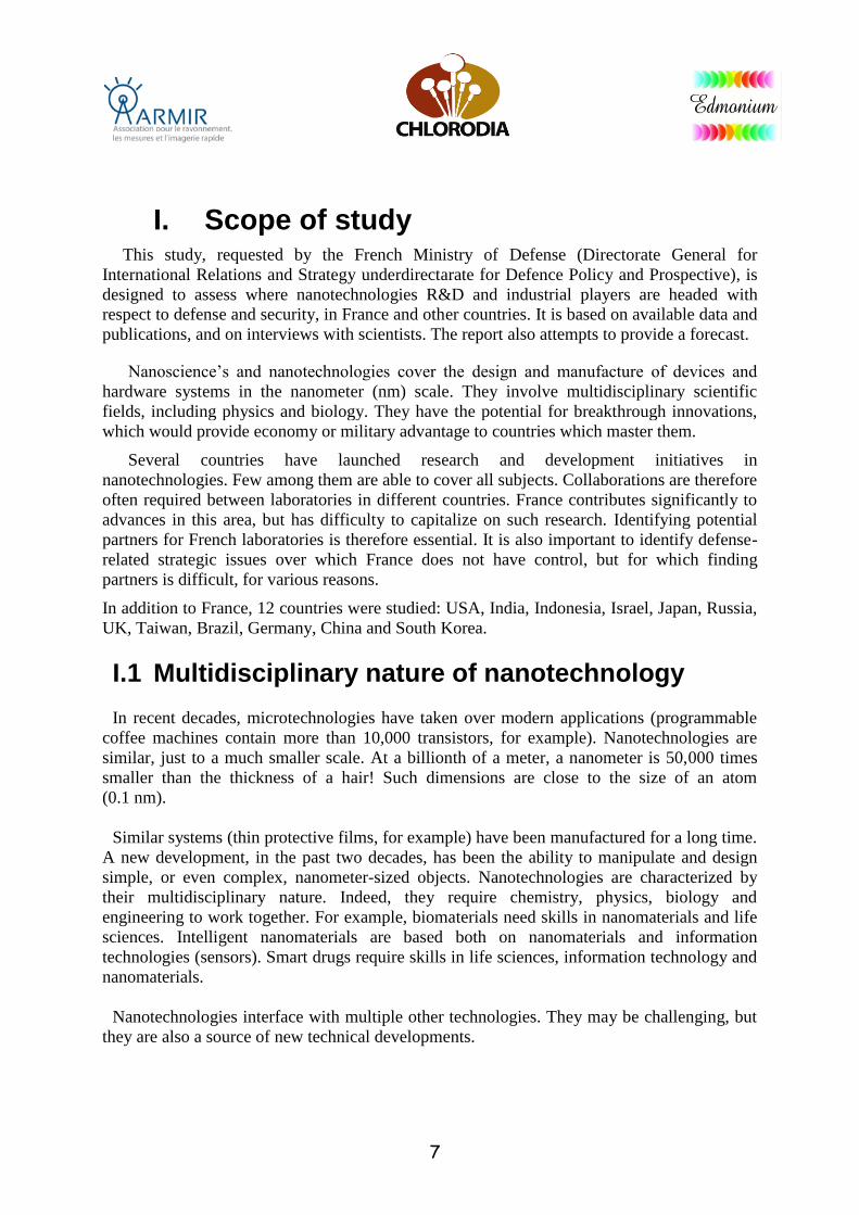
8
Figure 1. Interaction zone between materials and other knowledge areas. The larger the circle, the more
interaction there is.
Source: Rice University, USA; 2009.
Enthusiasm for nanotechnology arises from new features they give to materials. The smaller
an object is, the bigger its outer surface is with respect to its volume. Nanoscale objects are
characterized by an identical number of atoms in their surfaces compared to the number of
atoms with respect to volume. Surface phenomena thus play a predominant role. At the atom
scale, conventional physics is superseded by quantum physics. For example, Van der Waals
forces (cohesive strength of matter) predominate over gravity (since the mass of nanoparticles
is extremely low, gravity barely applies). Therefore, nanoparticles properties are different
from those of their macroscopic equivalents, such as for example:
higher melting point2 ;
better conductivity (depending on graphite sheet winding angle, a nanotube is either an
excellent conductor of electricity, or a semiconductor);
greater mechanical resistance (a carbon nanotube is 100 times stronger and 6 times
lighter than steel).
2Heating a solid agitates the molecules it is made up of. When agitation is sufficient, Van Der Waals forces that
keep the solid together break down. molecules remain in contact but become separated. Regular arrangement in
space disappears. Melting switches a solid to liquid state.
9
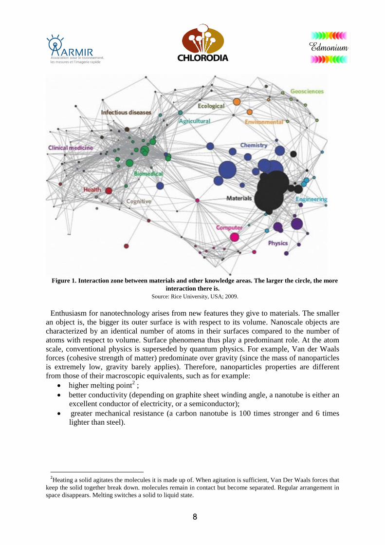
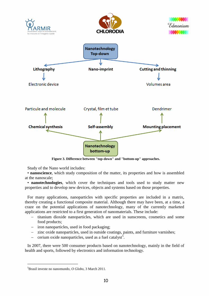
Two technological approaches are possible to fabricate nano-systems:
the first is the top-down approach; it involves cutting, carving or engraving a
material (such as a silicon wafer) to generate nano-sized objects, such as integrated
circuits produced by lithography3) ;
the second is the bottom-up approach, whereby nano-sized objects or systems are
assembled one atom after another, such as dendrimer synthesis4.
Figure 2. "top-down" and "bottom-up" approaches.
3 Lithography is a method whereby an image is printed on a flat surface; it is used in electronics.
4 Such nanoscopic sized macromolecules are characterized by a 3D structure; they are related to hyperbranched
polymers, in which branched monomers are associated according to a tree process around a multivalent central
core. They generally have a globular shape. In addition, solubility of such macromolecules is greater than
analogous linear polymers.
10
Figure 3. Difference between "top-down" and "bottom-up" approaches.
Study of the Nano world includes:
• nanoscience, which study composition of the matter, its properties and how is assembled
at the nanoscale;
• nanotechnologies, which cover the techniques and tools used to study matter new
properties and to develop new devices, objects and systems based on those properties.
For many applications, nanoparticles with specific properties are included in a matrix,
thereby creating a functional composite material. Although there may have been, at a time, a
craze on the potential applications of nanotechnology, many of the currently marketed
applications are restricted to a first generation of nanomaterials. These include:
titanium dioxide nanoparticles, which are used in sunscreens, cosmetics and some
food products;
iron nanoparticles, used in food packaging;
zinc oxide nanoparticles, used in outside coatings, paints, and furniture varnishes;
cerium oxide nanoparticles, used as a fuel catalyst5.
In 2007, there were 500 consumer products based on nanotechnology, mainly in the field of
health and sports, followed by electronics and information technology.
5Brasil investe no nanomundo, O Globo, 3 March 2011.
11
Nanotechnologies have a tremendous application potential, and are a wonderful laboratory
for understanding the world at the nanoscale. But, to make their application worthwhile, they
need to provide a significant advantage over existing technologies, either from the economy
or from the technology point of view. Thus, to replace a micro device, a Nano device needs to
provide one of the following benefits:
new features;
cost reduction while by providing the same functions;
significant performance increases at the same cost, or slightly higher.
Since many nanotechnologies may have both civilian and military applications, both areas
are closely related, and thus have a dual character. The use of civilian technologies in defense
can reduce costs, and may also reduce system obsolescence through state-of-the-art devices or
systems. Defense also has a trickle-down effect on the civilian field, albeit to a lesser extent
than it used to. However, it has the advantage, compared to the civilian field, of being able to
plan for the future by funding research which, while having no immediate applications, may
be of strategic interest for the long-term.
I.2 Health risks
Although nanotechnologies have advantages, they also may create risks to those who
manufacture or use them. There are different types of risks:
Most systems made up of nanomaterials do not pose a particular risk to users in
normal use. However, a risk may appear at the manufacturing level, if nanoparticles
are not entirely confined to prevent operators from contacting them. Also, during
deployment of nanostructured materials, at the end of their use or during
decommissioning operations, there is also a risk of nanoparticle dispersion. In defense
matters, there may also be a risk when use of nanoparticles cause them to disperse,
such as when using ammunition which generates them.
certain applications use nanoparticles and additives to prevent caking, such as in
certain foods, or sun tanning products containing TiO2 nanoparticles. Long term safety
guarantee is not fully established, especially after long periods of exposure.
12
I.3. Nanotechnology promises for defense and security
6
In addition to the many possible civilian applications, nanotechnologies may have defense
and security applications. Like in the civilian field, four areas have a large potential for
applications: energy Nano sources, nanomaterials, Nano electronics and Nano sensors.
New threats
Nanotechnology can be a source of new threats from countries or terrorist groups. These
threats may be chemical, biological, radiological (dispersion of radioactive products), nuclear,
or based on difficult to detect explosives.
Vectorization nanotechnology7 and Nano encapsulation
8 are being developed by the
pharmaceutical industry for making drugs and image contrast agents, and by the cosmetics
industry. Unfortunately, in the context of non-conventional weapons, technologies
developed to improve the administration of drugs can be used for the delivery of
biological or chemical agents. Nanotechnologies might thus help the militarization of
biological agents, toxins or chemicals, as follows:
- By preventing their fast degradation by air, sun or heat in the environment;
- By making it possible for such toxic agents to cross natural barriers preventing entry
into the body (blood-brain barrier or blood-tissue barrier, e.g.);
- By transporting and targeting toxic agents to specific cells or organs, thereby reducing
the doses necessary to achieve lethality, thus providing for new carriers such as water
and food;
- By facilitating release or activation of biological agents in desired amount at the
desired time;
- By making agents undetectable and unidentifiable (by masking the sites recognized by
detection tools).
Many of these options would eliminate operational difficulties encountered during the
production of such weapons, and could therefore make them easier to use. Moreover,
production of nanomaterials has increased significantly in recent years, and large quantities of
these are now available on the market. Meanwhile, prices of these materials have been falling.
6Chapters 11 and 13 are drawn from the study: "Outlook in Strategic partnerships between France and Brazil in
nanotechnologies" Ariane Castel, Chlorodia Company, May 2013. 7 Those act as a carrier for a bioactive molecule, which is attached to, or incorporated into, nanomaterials
(certain polymers, carbon nanotubes, inorganic nanoparticles, etc.). Such materials can bind to receptors and
enter into cells. This greatly improves the efficiency of the bioactive molecule. 8 A bioactive molecule is contained within a capsule. This technique provides stability to an unstable bioactive
molecule, allowing it to be transported, as well as timed and controlled release.
13
Nanotechnologies therefore make up a new threat requiring regulatory changes, in particular
export controls.
New opportunities
Fortunately, nanotechnology can also improve detection and countermeasure devices
(detection of nuclear, radiological, biological, chemical and explosive attacks, as well as
neutralization of espionage devices). Miniaturization allowed by nano devices enables
development of discrete, low-cost and low-power consumption information gathering
systems. To allow wide deployment, sensors must be inexpensive. This is where
nanotechnologies can make the difference with microtechnologies, since mass production
reduces costs while increasing device reliability and portability.
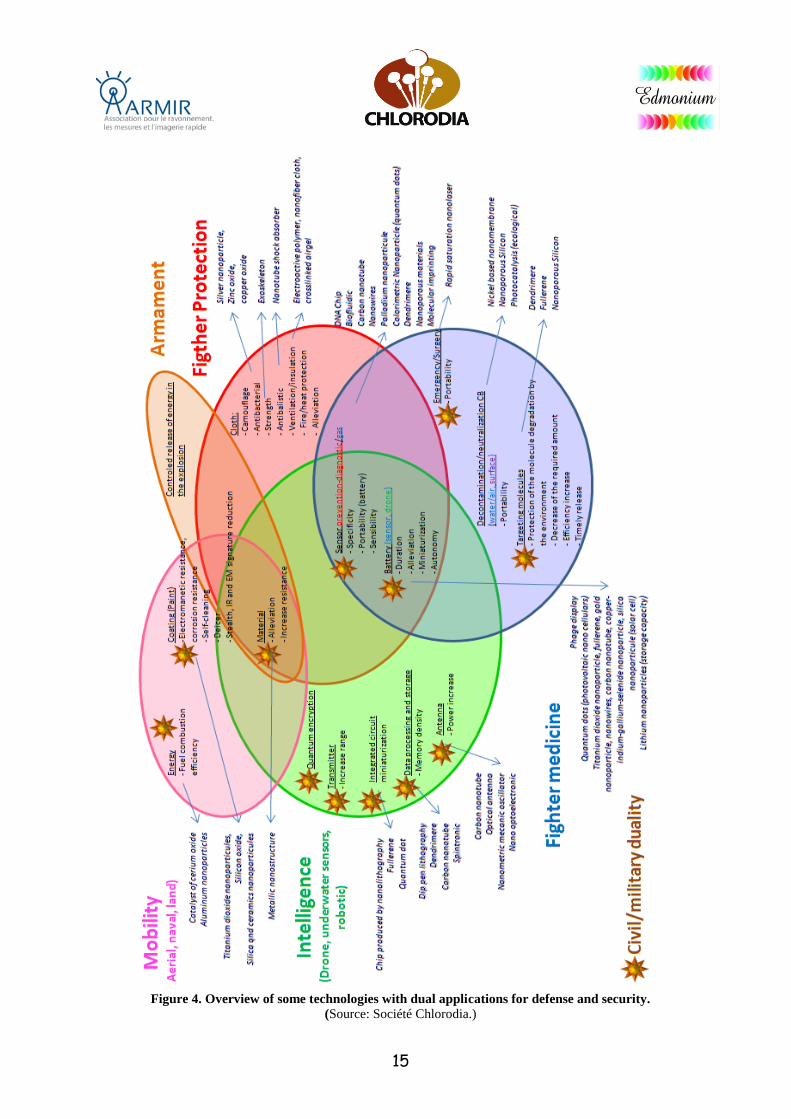
Figure 4 shows relationships between some technologies and some defense and security
needs. It shows items with dual applications.
This diagram shows the strong duality of nanotechnologies. For example, metallic
nanostructures (nanomaterials) which help making missiles lighter are also useful for
vehicles, aircraft or drones.
Moreover, it shows how mastery of a technology such as carbon nanotubes opens up to
numerous applications: improved battery performance, miniaturization of antennas and
storage memory, increased sensor sensitivity, and many others.
The diagram also shows how some capabilities are at the intersection of various fields of
applications (such as batteries and materials); mastering those would impact many areas.
Nanomaterials may also find applications in protection systems, either as reinforcement or
armor against projectiles, or as skin providing stealthiness, with some nanostructures.
Nanoelectronics makes production of miniaturized components possible, providing for
increased redundancy of electronic system, thus improving reliability.
Portable energy sources are the weak point of most nomadic devices requiring energy. Such
power sources must have a large energy density per volume and mass units. Volume and mass
do not always go hand in hand. Hydrogen, for example, which is a much talked about energy
carrier, has a high energy density per unit mass (33.3 kWh/kg, i.e. about three times that of
gasoline) but a low energy density per unit volume (1 kWh/L at 350 bar, i.e. 10 times less
than a liter of gasoline). Energy sources must be able to recharge quickly, must be strong,
reliable and able to withstand extreme conditions such as temperature, radiation, etc.
Portable power sources include batteries, which can be made with many different
technologies. Li-Ion technologies have become predominant, thanks to their good
performances. However, 1 kW/hr requires 5 kg of batteries to provide the same energy as
700 grams of gasoline.
Pairing battery technology with a smart "power management system" based on miniaturized
electronic components is important to increase battery performance, durability and reliability
for specific missions. Supercapacitors, a complementary technology, also can provide power
while having a practically infinite number of duty cycle compared to batteries.

14
A number of technologies provide for recovery of unavoidable energy, such as ambient heat,
vibration during movement, light, etc. Such technologies, although still emerging at the
industrial level, should develop in the coming decades. A case in point is thermoelectricity,
which requires nano-engineering to achieve interesting performance for low-cost applications.
Nano catalysis is a strategic process area, providing a strong economic benefit through lower
costs and improved ease and efficiency of chemical reactions; it can even make some
chemical reactions industrially feasible.
15
Figure 4. Overview of some technologies with dual applications for defense and security.
(Source: Société Chlorodia.)
16
II. Regulatory framework
This section contains an outlook of the current legal framework which can, to some extent,
impact France’s industrial and defense capacities, penalizing its industries, particularly in
terms of nanotechnology exports and imports.
II.1 Preamble
Current scientific research practices require researchers to publish and apply their
discoveries quickly, which inevitably leads to dissemination of information and development
of products before any potential restrictions for security purpose may be imposed.
In the nineteenth century, Pasteur replaced the “principle of foresight,” which was based on
the notion of good or bad luck associated with an individual, by the prevention principle,
based on scientific estimates of the spread of diseases in human groups. This prevention
principle itself was replaced, in the twenty-first century, by the precautionary principle when
Society took notice of uncertainties inherent to understanding of our world, scientific as it
might be. Said precautionary principle, now part of the French Constitution, now causes over-
control, as it tends to be applied to anything new, including nanotechnology9. Although
current nanotechnology-related regulations are still minimal, they are expected to grow in the
near future.
In addition to the above precautionary principle, itself based on uncertainty about the effects
of nanotechnologies, other economic- or defense-related considerations have been added.
They involve standards restricting nanotechnology data and products. The potential impact of
such growing restrictions on our industrial and defense capacities will be examined.
II.2 Regulatory constraints
As international, European and French laws are constantly changing, three types of
motivations leading to nanotechnology-related laws can be identified:
• The primary motivation is protection of people and the environment due to the
relative ignorance about the danger of some nanomaterials whose effects might be disastrous
in the medium or long term. This caused development, as a direct result of the precautionary
principle, of a European regulation which has yet to be transposed into French law.
France’s Executive Order 2012-232
Because of unfamiliarity regarding danger of certain nanomaterials, the Ministry of Ecology;
Sustainable Development, Transport and Housing has taken measures concerning production,
distribution and import of substances in the nanoparticulate state (Executive order no 2012-232 of 17
February 2012). This implementation order is the mere transposition into French law of European
Regulation 1907/2006 of the European Parliament and of the Council of 18 December 2006. It sets the
amount of nanoparticles above which reporting is mandatory at a threshold of 100 g.
9 Thérèse Leroux, Le Principe de précaution et le questionnement que suscite la nanomédecine, in Christian
Hervé, Michèle S. Jean, Patrick Molinari, Marie Angèle Grimaud, Emmanuelle Laforêt, La Nano-médecine.
Enjeux éthiques, juridiques et normatifs, Ed. Dalloz, Paris, 2007.
17
• A second motivation arises from the desire to control production and trade of
nanomaterials which can be used to develop defense, attack or protection equipment, or for
terrorist purposes, and might lead our partners or our foes to gain an edge over our national
capacities, or would even allow non-state groups to develop terrorist capacities.
• The third motivation arises from the will of some international industrial groups to
keep for themselves any financial benefits provided to them by production and sale of certain
nanomaterials, or any derived goods.
Faced with this trend whereby laws keep being expanded, undesirable consequences of
implemented regulations should be considered. Indeed, some nanomaterials may prove
essential in nano-medicine, in the pharmaceutical industry, for the treatment of certain
diseases, or to decrease chemical pollutants. In technological and industrial terms,
nanomaterials may also cause major developments in our understanding of the world or the
behavior of our societies.
More specifically, we want to avoid some of the negative effects induced by excessive
regulation. For example:
• Restrictions should penalize neither basic university research nor French
industries R&D. In particular, no regulations should cripple the flow of information or the
movement of goods required for said research.
• Restrictions should not cripple French defense industry by preventing French
companies from exporting some products, while preventing them from gaining contracts
essential to their survival.
• Controls should not restrict growth of French civilian industry through complicated
waiver procedures or making them wait longer for government’s approval.
Regulations are implemented in three ways:
• Control can be based on lists of goods; such lists can be international, European or
French. Such lists, based on descriptions as accurate as possible, of the goods to be restricted,
need to be updated continuously, based on technical developments and introduction of new
materials.
• Thresholds of material quantities beyond which the control should apply also need to
be defined. Such thresholds also need to be adjusted from time to time based on impact
studies.
• Finally, a control system for checking proper application of the law needs to be
implemented. Such regulatory agency must possess technical and legal powers to analyze
applications made by companies, and grant any required authorization within a reasonable
time.
18
Export and import control of dual-use goods
Control of dual-use goods
Exports and imports of Dual-use goods (DUG) are highly supervised by law.
DUG are goods which, based on an international definition, are subject to restrictions and export
control because they could be used for design and manufacture of conventional weapons or weapons of
mass destruction.
Such lists are made up by international agencies, such as:
NSG (Nuclear Suppliers Group) for nuclear weapons, MTCR (Missile Technology Control Group), AG
(Australian Group) for chemical and biological weapons and Wassenaar Agreement (WA) for
conventional weapons.
Said four lists are concatenated at the EU level; they have been published in European Regulation No.
388/2012 of 19 April 2012.
DUG export control lists are continuously revised and updated to account for advances in technology.
Development of nanotechnology is impacted significantly by such control lists. Indeed, almost all of the
ten categories of goods in Regulation 388/2012 use nanotechnology, in particular categories 1
(Materials, Chemicals, “Microorganisms” and “Toxins”), 2 (Materials treatment), 3 (Electronics) and 6
(Sensor and Lasers).
Taking electronics, which includes photolithography chip manufacturing, as an example, it appears that
France controls export of measuring and chip manufacturing tools, as well as export of some raw
materials. However, some of our foreign partners have implemented the same export controls, which
may have a direct impact on some of our imports.
Because of such updates to the lists of controlled goods, French government, as well as our
companies, need to take an active part in related international and/or European bodies to
defend our legal and technical interests.
Evolution of monitoring strategies for control lists
Experience has shown that three types of strategies may emerge within international bodies.
• A first strategy aims to reinforce non-proliferation policies, and to fill gaps of in lists
by adding items, and / or, if necessary, widening technical parameters of already-listed goods.
• A second strategy, on the contrary, aims at preserving industry and trade, and
promotes easing of controls.
• A third type of strategy reduces controls of obsolete technologies and strengthens
controls on technologies one is the only to master.
19
It is notable that countries attitudes evolve according to their threat perception and
evaluation of their foreign trade.
Current trend within the Wassenaar Arrangement (WA), is to move towards a general easing
of control, as demonstrated by the number of “non-control” proposals (about three quarters of
all proposals.)
However, it should be underlined that there are currently comparatively very little
discussions about nanotechnology within the WA.
Discussions about nanotechnologies are currently almost non-existent within NSG and
MTCR. In contrast, the Australia Group pays a close interest for the emergence of these
technologies.
For example, proposals toward regulating nano-fiber manufacturing machines are currently
being discussed.
Note: China is a member of NSG, and is seeking to be involved neither in the Wassenaar
Arrangement nor in other arrangements. India, on the other hand, is trying to be admitted in
the four export control systems.
There does not appear to be any current desire within the European Commission to question
DUG laws, which apply directly as such in each EU State. However there are still some
anomalies10
.
Some progress has been implemented within the EU, such as temporary export licenses to
take part in trade exhibitions.
Other international regulatory bodies
Biological Weapons Convention (BWC) and Chemical Weapons Convention (CWC) are
two international treaties that may be concerned by nanotechnology regulations. Both
Conventions have very structures.
CWC has a verification body (OPCW), while BWC has none. However, OPCW, which was
created to apply the Convention on Prohibition of Chemical Weapons (CWC) may only,
within the scope of its mandate, verify destruction of existing chemical weapons. It may
therefore neither concern itself with nanotechnologies nor their possible use in defense
applications.
Although BWC could deal with nanotechnologies, it has no verification system. In addition,
defining nanotechnology applications with respect to biology raises many problems
Should, for example, nanomaterials be defined based on their size (smaller than 100 nm),
which would include organisms like the smallest viruses, or should they be limited to inert
materials?
Potential applications of nanotechnologies to biology are numerous, including for defense11
.
10
The EU Treaty requires that each member countries apply BDU export controls, while some member
countries are not involved in certain schemes.
20
When it comes to the law, the speed of developments in nanotechnologies, which can be
measured in months, is hardly consistent with passing bills, which may require years of legal
arguments.
This is why, with respect to nano-medicine, some legal experts recommend, according to the
Declaration of Helsinki, implementing recommendations and a code of good practice, i.e. a
“soft law”, which would be less binding and much more flexible. Such an approach may have
disadvantages, but would prove in practice better for this new situation.
II.3 Monopolies and patents
Monopolistic approach by some of our foreign partners, French patents application
procedures, and the rather passive attitude of French companies, France might quickly lose all
benefits from the money spent on research and development which allows French businesses
to innovate, develop, manufacture, transform and export in the field of nanotechnologies.
Increasing monopoly by some countries
The past years have seen emergence of a quasi-monopoly on some Chinese electronic
components or raw materials.
Specifically, that country now controls over 40% of the worldwide production of
microprocessors.
Insufficient number of patents filed in France:
Low number of patents filed in France is partly due to the complexity and diversity of patent
legislation in different European countries.
Although a European patent application procedure was put implemented in Brussels, this
procedure does not replace national procedures; patent applications still need to be filed in
each European country in which one wishes to be protected. France has also the particularity
that a patent applicant cannot go directly to Brussel. This explains the difficulty to know
whether a patents has been filed in France by a French citizen or by a foreigner.
These drawbacks come in addition to a number of weaknesses in European and French
regulations, as well as France’s own export control structure, which can have a negative
impact on France’s export capacity in this field.
Conclusion
In general, existing regulations imposes a number of restrictions over research and
development of nanotechnologies; international restrictions are currently few, but are
expected to grow in coming years.
11
Their use for scattering or disseminating biological agents, for example, or targeting specific areas of the
body, may be mentioned.
21
Defining a long-term national strategy for developing certain branches, together with public
funding to be approved by all government agencies applicable, seems to be the essential factor
to promote nanotechnology growth.
Such national strategy will have to face raw material and component monopolistic
situations, a small number of patents filed, obsolescence of those products being banned due
to constant changes in law and a growing technology gap with some partners ; all these
factors have a damaging effect on the industry.
II. International situation and the place of Europe
Many countries are now investing in nanotechnologies because they believe the technology
may become a source of wealth and employment in the future. The field is growing
irreversibly all over the world. Any country not following this move will quickly become
outdated and dependent on other countries, with the risk of not being able to access a number
of technologies, or able to access them only in a degraded mode. Such a situation may prove
to be particularly damaging in the fields of defense and security.
Dependency on foreign countries may cause use restrictions, and therefore restrict actions as
well as slowing down or prevent required modification.
Nanotechnologies are an emerging, albeit strategic, in which all countries must find their
place based on resources and capabilities; this is why knowing how various countries fare on
the global level is important.
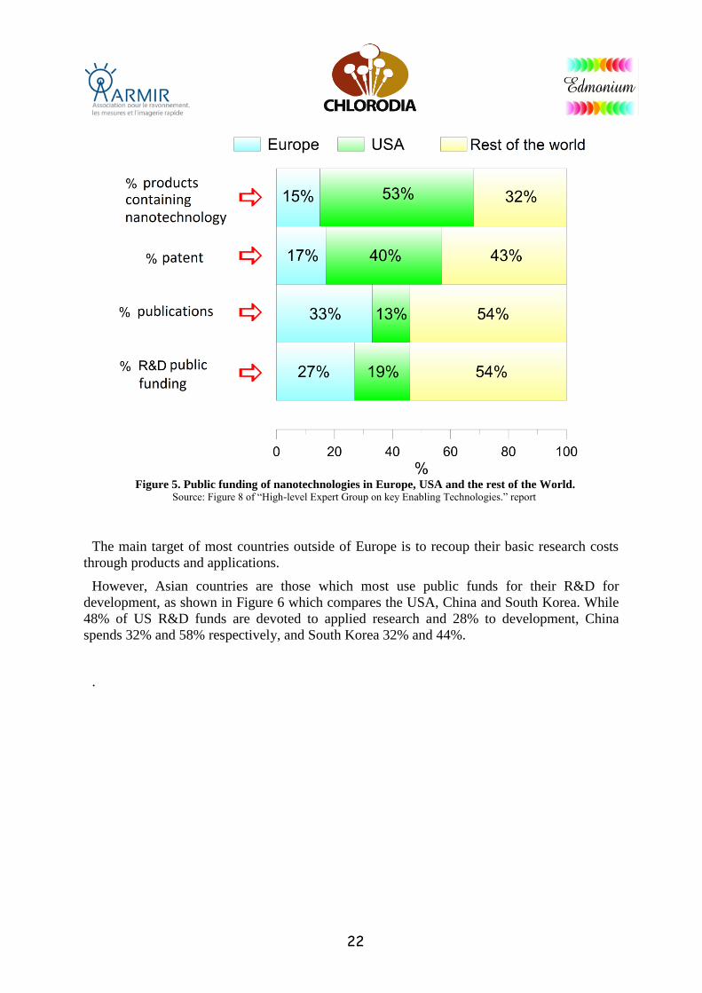
Discrepancy between industrial developments and research efforts is not specific to France.
The following Figure shows that, while the EU produces 33% of world publications in the
field of nanotechnology, it contributes only 15% of final products, i.e. those bought by
consumers. Europe is very good in terms of publications in basic research, but not when it
comes to marketing its ideas.
22
Figure 5. Public funding of nanotechnologies in Europe, USA and the rest of the World.
Source: Figure 8 of “High-level Expert Group on key Enabling Technologies.” report
The main target of most countries outside of Europe is to recoup their basic research costs
through products and applications.
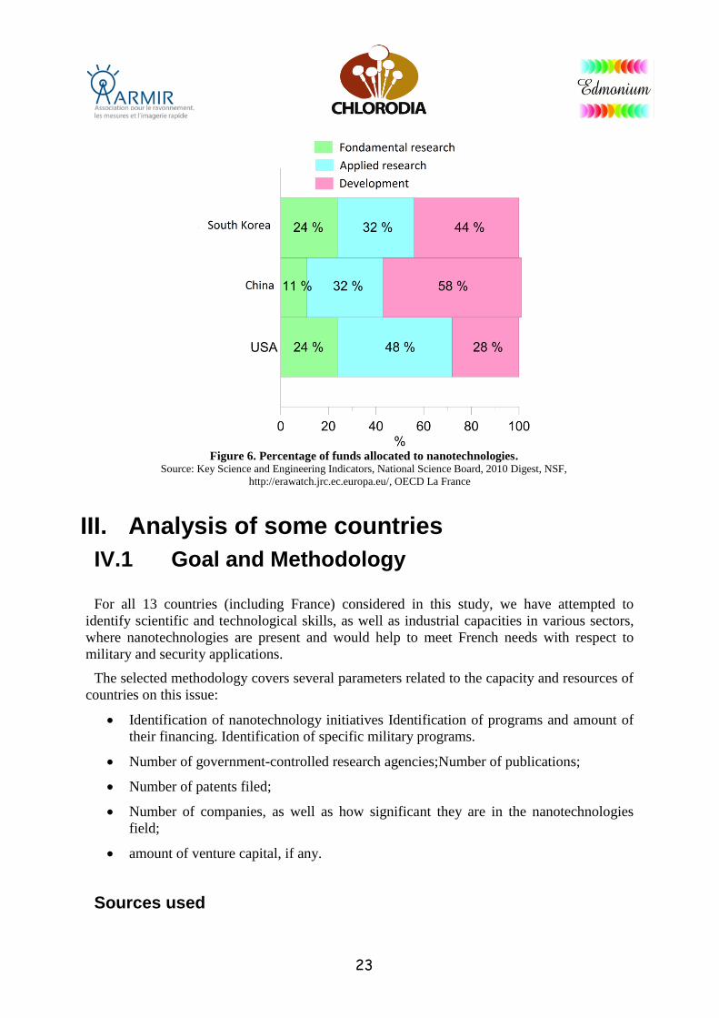
However, Asian countries are those which most use public funds for their R&D for
development, as shown in Figure 6 which compares the USA, China and South Korea. While
48% of US R&D funds are devoted to applied research and 28% to development, China
spends 32% and 58% respectively, and South Korea 32% and 44%.
.
23
Figure 6. Percentage of funds allocated to nanotechnologies.
Source: Key Science and Engineering Indicators, National Science Board, 2010 Digest, NSF,
http://erawatch.jrc.ec.europa.eu/, OECD La France
III. Analysis of some countries
IV.1 Goal and Methodology
For all 13 countries (including France) considered in this study, we have attempted to
identify scientific and technological skills, as well as industrial capacities in various sectors,
where nanotechnologies are present and would help to meet French needs with respect to
military and security applications.
The selected methodology covers several parameters related to the capacity and resources of
countries on this issue:
Identification of nanotechnology initiatives Identification of programs and amount of
their financing. Identification of specific military programs.
Number of government-controlled research agencies;Number of publications;
Number of patents filed;
Number of companies, as well as how significant they are in the nanotechnologies
field;
amount of venture capital, if any.
Sources used
24
Data collection has mainly relied on the following four sources:
Identification of the numbers of patents filed in nanotechnologies for the studied
countries:
To assess the scientific and technical level in all nanotechnology-related fields for the
studied countries, our research was based on the number of patents filed between 2000 and
201112
. Relevance and comprehensiveness of the results depend upon the search terms
selected, which can focus on various criteria.
Due to the vast number of concepts covered, it was decided to focus the search on:
words beginning with “nano” in the title or the abstract; classification codes B82B,
B82Y and H01F-41/30 of the International Patent Classification, codes which cover
the following categories: “Nanotechnology” and “Equipment or processes for applying
nanoscale structures”;
classification code 977 (main class and additives) of the US classification of
nanotechnology patents.
Systematic use of Nanowerk dedicated database:
This base offers the advantage of containing worldwide data and to be updated frequently.
This USA-based web site, launched in 2005, is mainly funded by subscribing partner
companies. However, we believe that these companies make up only a portion of all
nanotechnology companies. We have deemed that such partial coverage does not impact
business-segment based analysis, especially since an additional list of companies has been
incorporated into the analysis process. Furthermore, it does not appear that any bias which
would favor specific a business segment has been introduced.
Searching for information on the Internet:
Search was based on identified countries and topics of interests, in order to expand the
database above. For example, the “company data rex” web site (similar to France’s
Infogreffe) has been used for the United Kingdom; the “MATIMOP - The Israeli Industry
Center for R & D” web site was used for Israel; the “Made in China” website which
references Chinese who want to market these products abroad, has been used for China, etc.
Experts were contacted during the course of the study to obtain additional information
on specific countries, in particular France, Germany and Israel.
Data selected
With respect to patents, we have extracted from the abovementioned research, for each
country and for each year:
12
The research was made on the industrial property portal Questel-Orbit server that allows access to nearly all
patents filed worldwide, including the countries of interest to us. CEA, which has kindly provided a access right
to the server for the research carried out, deserves to be thanked.
25
1. the number of patent applications based in applicant’s country of origin13
;
2. Applications filed with patent offices in the studied countries. Such applications may be
filed by in-country organizations14
and by foreign companies and R&D centers filing in
these countries;The ratio of applications filed by in-country organizations.15
With respect to companies, overall indexing was done for each country, based on 14
business segments involving a degree of nanotechnologies:
(Chemicals) [photocatalysis, pigments, green chemistry]; (Basic products)
[nanopowders, nanotubes];Construction [building materials (glass, insulation,
paints, protection against wear), concrete (curing agent, sealing compound,
repair mortar, steel, etc.)];
Energy [power distribution (heat transfer, etc.), energy production (fossil fuels,
fuel cells, gas turbines, solar cells, wind turbines, etc.), energy storage
(electricity, batteries, ultracapacitors, etc.), energy use (light emissions, etc.)];
Environment [carbon capture, filtration (potable water), sanitation
(decontamination, oil spills management, etc.), wastewater treatment];
Food [food wrap (packaging materials, etc.), food processing (filtration, etc.)]
Information Technologies and Communication (ITC) [data storage,
electronic display, coatings (lithography, computer chips, heat sinks, ink jet
printing, etc.), polymer filters, optics, photonics, semiconductors];
Medicine [therapeutic and antimicrobial agents, dental care (implants), drug
delivery, pharmaceutical products (catalysts, etc.)];
Precision engineering [coatings (nanofilms), metrology, optics];
Textiles and clothing [coatings, protection];
Transport [automotive (adhesives, engines, membranes, paint, parts, steel,
wear protection, etc.), marine]
Sensors [diagnosis / R & D (microfluidic; contrast agents, X-ray probes, etc.),
environmental analysis (air, water, etc.);
(Services: consulting, R & D, technology transfer, etc.)
We have considered that 10 (those not between parenthesis in the list) of the 14 analyzed
segments had military or security potential application; they are those which were selected
for the analysis.
Among analyzed countries, the USA represents a special case: the vast initial quantity of
data (over 1,100 companies) did not allow a full analysis because the budget available for the
13
All filing procedures taken into account: national, European and global offices 14
Laboratories & industrialists. 15
Laboratorie & industrialists.
26
study could not provide an adapted automatic search engine. Sampling16
was used to divide
the number of examined companies by 10; the hundred or so companies thus selected allowed
the USA to be analyzed on the same basis as the other countries.
Usage
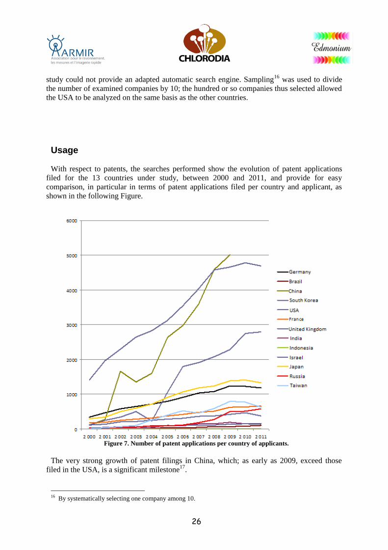
With respect to patents, the searches performed show the evolution of patent applications
filed for the 13 countries under study, between 2000 and 2011, and provide for easy
comparison, in particular in terms of patent applications filed per country and applicant, as
shown in the following Figure.
Figure 7. Number of patent applications per country of applicants.
The very strong growth of patent filings in China, which; as early as 2009, exceed those
filed in the USA, is a significant milestone17
.
16
By systematically selecting one company among 10.

27
Moreover, with respect to paragraphs 2) and 3), relating to applications filed with patent
offices, the results of the two filters used are limited to data from national patent offices.
These results are no less interesting, freeing the native part of deposits from the foreign one,
reflecting to a certain degree, the potential attractiveness of the countries. The evolution of the
number of patents going from 2000 to 2011 in all three possible types is shown for each
studied country. 18
A database listing all19
identified companies analyzed in the study was created.
The first piece of data from this database is the total number of currently-identified
companies per country20
..
Other data covers the number of nanotechnology companies created each year in the past
twenty years. This research was done for each studied country, based on company creation
dates.
The corresponding chart is included in each21
country's data sheet.
It shows that company incorporation charts can be split into three categories:
The leading group,
composed of:
1. United States (for which
only 10% of companies
have been sampled);
2. Germany
3. United Kingdom
Figure 8. Number of nanotechnology companies created each year
by the top group of countries. Source: Société Chlorodia.
17
An article from the French Embassy, however, calls for caution, considering that until recently the
innovative character of the applications did not always appear sufficiently. Starting in 2010, a procedural reform
of national patent filing seems to have taken place to get closer with the practices of other countries. 18
See the related country profiles. 19
The means implemented in the study did not make it possible to highlight existence of an industrial fabric in
the field of nanotechnology in Brazil and Indonesia. 20
See the corresponding country files. 21
.Except Brazil and Indonesia, because no nanotechnology company was identified in these countries.
28
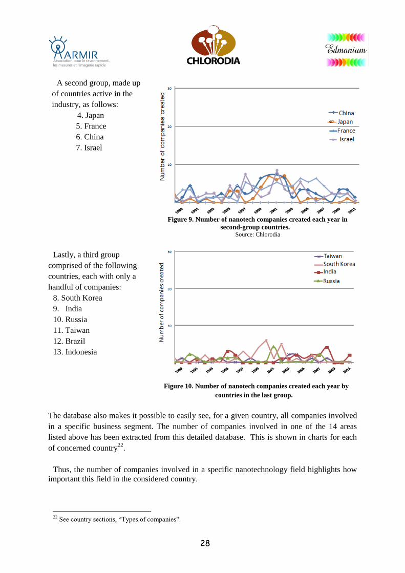
A second group, made up
of countries active in the
industry, as follows:
4. Japan
5. France
6. China
7. Israel
Figure 9. Number of nanotech companies created each year in
second-group countries. Source: Chlorodia
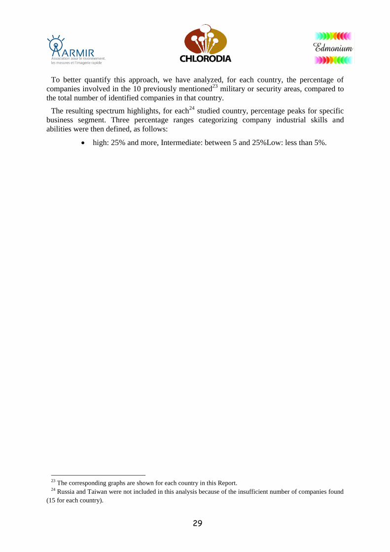
Lastly, a third group
comprised of the following
countries, each with only a
handful of companies:
8. South Korea
9. India
10. Russia
11. Taiwan
12. Brazil
13. Indonesia
Figure 10. Number of nanotech companies created each year by
countries in the last group.
The database also makes it possible to easily see, for a given country, all companies involved
in a specific business segment. The number of companies involved in one of the 14 areas
listed above has been extracted from this detailed database. This is shown in charts for each
of concerned country22
.
Thus, the number of companies involved in a specific nanotechnology field highlights how
important this field in the considered country.
22
See country sections, “Types of companies".
29
To better quantify this approach, we have analyzed, for each country, the percentage of
companies involved in the 10 previously mentioned23
military or security areas, compared to
the total number of identified companies in that country.
The resulting spectrum highlights, for each24
studied country, percentage peaks for specific
business segment. Three percentage ranges categorizing company industrial skills and
abilities were then defined, as follows:
high: 25% and more, Intermediate: between 5 and 25%Low: less than 5%.
23
The corresponding graphs are shown for each country in this Report. 24
Russia and Taiwan were not included in this analysis because of the insufficient number of companies found
(15 for each country).
30
IV.2 France IV.2.a Basic data
Population (2010) 64 millions
Surface area (mainland) 547,000 sq. km
Average population density 112 residents /sq. km
GDP (2011) USD 2,800 billion
GDP per capita (2011) USD 43,700 $
HDI (2011) 0.872
IV.2.b France’s efforts
France decided, a few years ago, to mobilize significant resources, including dedicated
agencies, to develop areas of expertise in nanotechnologies. As early as 1999, the French
government set up a National Micro-Nano Technology Network (RMNT) with a view to
improving interfacing of government-funded and private research. These efforts have grown
over time, and France is beginning to reap returns on this investment.
Sustained efforts
Since 2003, National Network on Nanoscience’s and Nanotechnologies (R3N) has been
implementing a support plan for a network for large-scale manufacture of nano-structures.
R3N’s is tasked to finance leading projects through a network of university research labs and
partnerships between government-funded laboratories, innovative SMEs and R&D centers of
large companies. A major Basic Technological Research (RTB) program, involving CNRS
and universities technology centers (RENATECH25
network) and CEA / LETI, was
implemented.
In 2005, National agency for research (ANR) initiated a national nanotechnology program
(PNANO), whose implementation is based on R3N. Technological research and innovation
networks (RRIT), also supported by ANR, are also involved in micro- and nanotechnologies
(RMNT network) and nanomaterials (RNMP network).
France’s Ministry of Research currently supports creation of centers of excellence in
nanoscience “C’NANO”. Currently there are six such centers of excellence, in the following
regions: Ile de France - Great East - Rhône Alpes - North West - Great South West - PACA.
The French government has recently retained 67 projects dedicated to micro-
nanotechnologies and software technologies that are among the six world-class projects. In
France, the major tool promoting commercialization of government-funded research is the
Law of July 12, 1999 for innovation and research. This law includes a section dedicated to
25
www.rtb.cnrs.fr
31
cooperation between government-funded and industrial research. Said section allows public
science institutions (such as CNRS) to create “industrial and commercial activity services”
(SAIC) to manage their research contracts and those involving private companies. SAICs may
also manage delivery of services to outside customers.
The Law of July 12, 1999 has been amended over the years. As an example, since 2006, the
National Research Agency (ANR) may fund research project partnerships between
government institutions and private companies. Such funding is targeted in priority to those
strategic research areas where private business research effort is considered insufficient
(nanotechnologies, for example).
Current funding actions include P2N (financed by ANR), and Nano 2012, initiated in 2008,
which combines the R & D centers of IBM, ST-Microelectronics and CEA / LETI. There is
also Nano-INNOV, detailed further down. Yearly budgets are €90 million for the P2N
program, €20 M for Nano2012 and €20 M for Nano-INNOV. The government also supports
development of large infrastructures via Labex (laboratories of excellence) and Equipex
(equipment of excellence). During the last decade, France’s effort to grow science
partnerships was Paris-centric. However, the government has recently become aware of the
need to allow greater flexibility to local stakeholders (which is partly reflected in the
“competitiveness centers” policy).
Nano-INNOV
Nano-INNOV is an effort to encourage development of nanotechnologies in France. A
large-scale investment plan was introduced in 2009 to create centers of technological
integration, similar to the Grenoble center involving micro- and nanotechnologies.
Development of three such integration centers was started in Grenoble, Toulouse and Saclay.
The most recent one, Nano-Innov Paris Region, opened in 2012. This center involves nearly
700 researchers, engineers and technicians. It is dedicated to design and manufacture of
innovative systems incorporating both nanotechnology and software.
These three integration centers have their own specialization, as well as transverse activities.
In 2005, about 5300 researchers in 243 laboratories were working in the field of
nanotechnology. In France, the 4 larger areas involved in nanotechnology are those of
Grenoble, Toulouse, Lille and Paris, supplemented by other smaller regional laboratories.

32
Figure 11. Distribution of French agencies controlling a European nanotechnology project.
Black numbers on the pins indicate the department number, pin color shows class and number of
projects.
Concentration of activities related to the development of nanotechnologies in France is
noticeable. In 2005, there were nearly 2000 scientists in Ile-de-France, nearly 1000 in Rhône-
Alpes and Great South-west, and about 500 in Great East, the North West and the PACA
regions.
IV.2.c Resources to match goals
The field of nanotechnologies is multidisciplinary, requires large investments and good
relationship with manufacturing. Excellence in basic research by itself is not enough; research
results must be marketed for revenue and employment to created. France's technological
fabric in this area has improved significantly over the past decade and now features
laboratories, facilities and tools allowing ambitious goals to be set.

33
From ad hoc research to collective effort
France has good basic research laboratories, but they are working on scattered topics, and
the chain of elements required for research to evolve into a finished product or to obtain
lasting industrial sectors is often missing.
For example, even though some of a laboratory research may be able to be manufactured by
industry or defense, this is not the lab’s primary objective which is to publish research papers
and, if possible, to file patents.
It may happen that a manufacturer or the Defense department requests help to solve specific
problems from a laboratory known for its expertise. However, there's usually no overall
strategy for reaching a goal in an industrial area.
Reaching critical mass
To cover most bases, and to be able to respond to very diverse problems, many basic blocks
need to be available so they can be put together to match requirements.
This requires a critical mass of research, as well as dedicated organization to promote
development and industrialization, including creating a start-up company if necessary.
Collaborative, rather than separate, efforts are therefore necessary for international visibility
and efficiency.
A benefit of such an agency would be having very large powers allowing developments that
can't be achieved by specialized labs.
As a matter of fact, innovation, by and large, now originates from multidisciplinary
research. Example: there are excellent laboratories working on batteries; other labs work on
integrated electronics. Combining both skills would allow batteries with optimal performance
and life to be made.
The three key areas of nanotechnology are characterization, modeling-simulation and
manufacturing. Like a manufacturing critical mass is required to be competitive
internationally, critical mass is required for modeling-simulation and characterization,
Manufacturing
We will not delve about manufacturing of nanodevices, nanomaterials, etc., since the
government and research contracts with industry have made development of several
technology centers in France possible.
Characterization
Even though each laboratory may have their own characterization systems, financial reasons
won’t allow to do everything. Therefore, large nationwide characterizing laboratories, with
the best performing tools, are necessary,. Such devices, with the best possible resolutions and
sensitivities, provide for any characterization not feasible by labs own resources. Indeed, the
cost of maintenance contracts for such complex devices are too high for small laboratories,
and detrimental for their productivity.

34
Beyond standard characterization means, synchrotron-generated radiation and neutrons are
also irreplaceable in some cases for characterization.
France owns the SOLEIL synchrotron, and has access to EU-owned ESRF in Grenoble.
SOLEIL covers from far-infrared to X-rays, and ESRF from UV to very hard X-rays. LLB (in
Saclay) may be used for neutron generation.
Simulation
For modeling-simulation, the need for a critical mass arises from the ever-growing
requirement for intensive computation devices involving thousands of elementary processors.
Parallelization of calculation codes has become a specialized job requiring specific facilities
with large computing resources.
A specialist is now required to effectively optimize a calculation code on a massively
parallel machine with multicore processors and graphic processors.
IV.2.d Publications and patents
A known problem is that France can create knowledge but usually fails to convert such
knowledge into wealth. This can be illustrated by comparing the number of scientific
publications and patents of France and South Korea (Figure 12).
Figure 12. Comparison of scientific publication and patent numbers between France and South Korea.
From Nano-INNOV report, 2008.
In many scientific fields, France has good quality basic research, but fails to convert
research into its potential industrial production. For the 20002010 decade, France’s number of
patent applications has stagnated in all fields. At the same time, China experienced strong
growth and has overtaken France in 2010. The tax credit for research has had a slightly
positive impact in the years 2008, especially for SMEs, but with only a small increase on the
number of patents filed. France files, on average, three times fewer patent applications than
Germany. This correlates with the fact that French industry is about three times smaller than
German industry. It is also a symptom of France’s gradual deindustrialization.
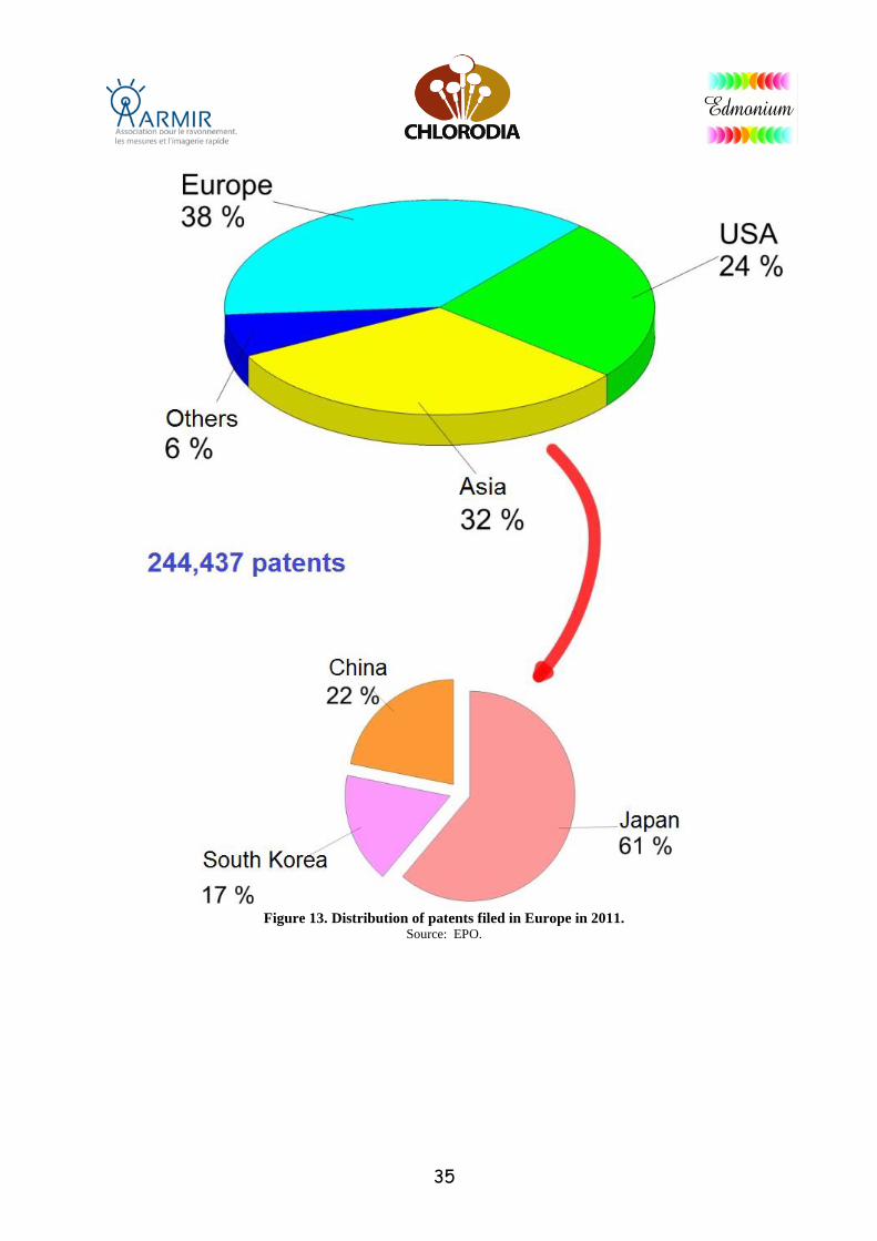
At a European level, over 60% of patents filed in Europe are the work of non-European
countries, as shown in Figure 13. Of the nearly 250,000 patents filed in 2011, 32% were filed
by Asian countries. The lower part of the Figure shows the distribution of patent filings by
Asian countries (Japan, South Korea and China.)
35
Figure 13. Distribution of patents filed in Europe in 2011.
Source: EPO.
36
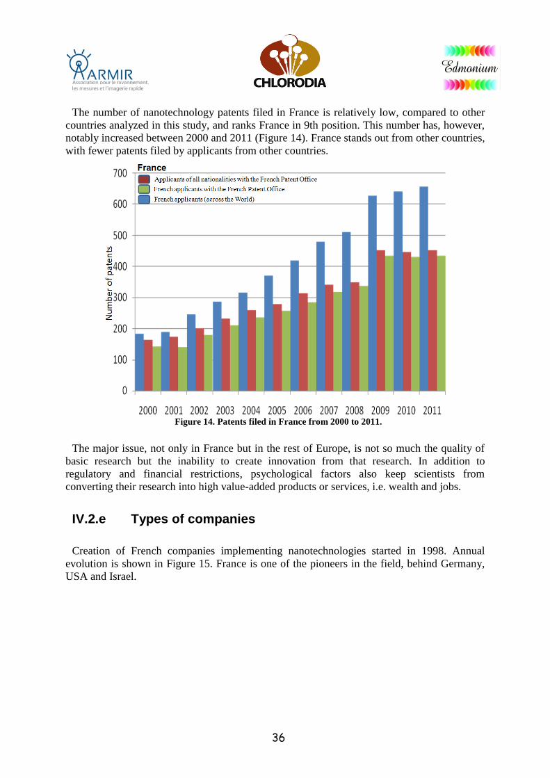
The number of nanotechnology patents filed in France is relatively low, compared to other
countries analyzed in this study, and ranks France in 9th position. This number has, however,
notably increased between 2000 and 2011 (Figure 14). France stands out from other countries,
with fewer patents filed by applicants from other countries.
Figure 14. Patents filed in France from 2000 to 2011.
The major issue, not only in France but in the rest of Europe, is not so much the quality of
basic research but the inability to create innovation from that research. In addition to
regulatory and financial restrictions, psychological factors also keep scientists from
converting their research into high value-added products or services, i.e. wealth and jobs.
IV.2.e Types of companies
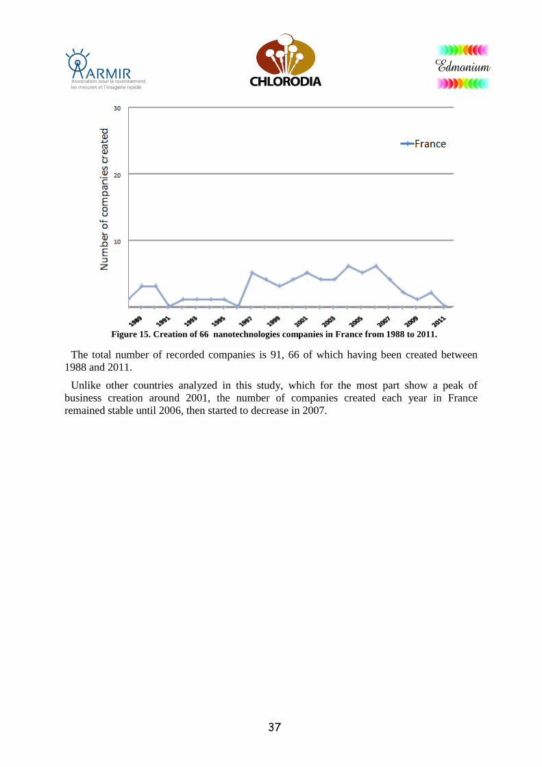
Creation of French companies implementing nanotechnologies started in 1998. Annual
evolution is shown in Figure 15. France is one of the pioneers in the field, behind Germany,
USA and Israel.
37
Figure 15. Creation of 66 nanotechnologies companies in France from 1988 to 2011.
The total number of recorded companies is 91, 66 of which having been created between
1988 and 2011.
Unlike other countries analyzed in this study, which for the most part show a peak of
business creation around 2001, the number of companies created each year in France
remained stable until 2006, then started to decrease in 2007.
38
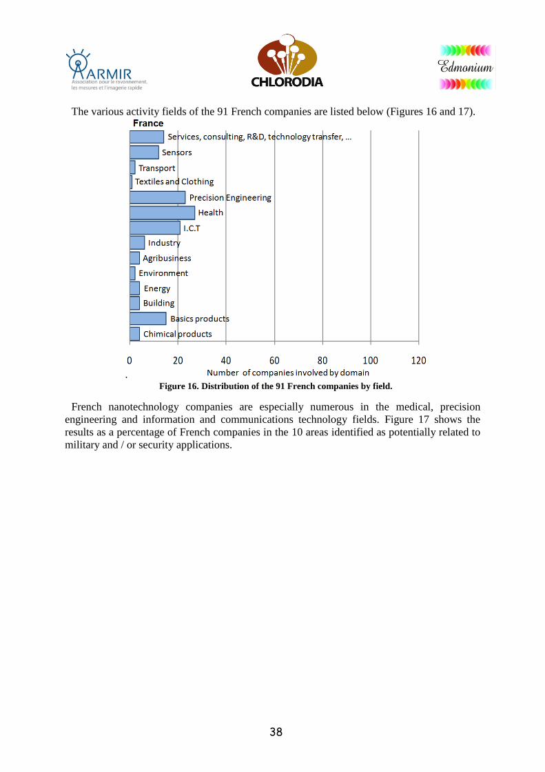
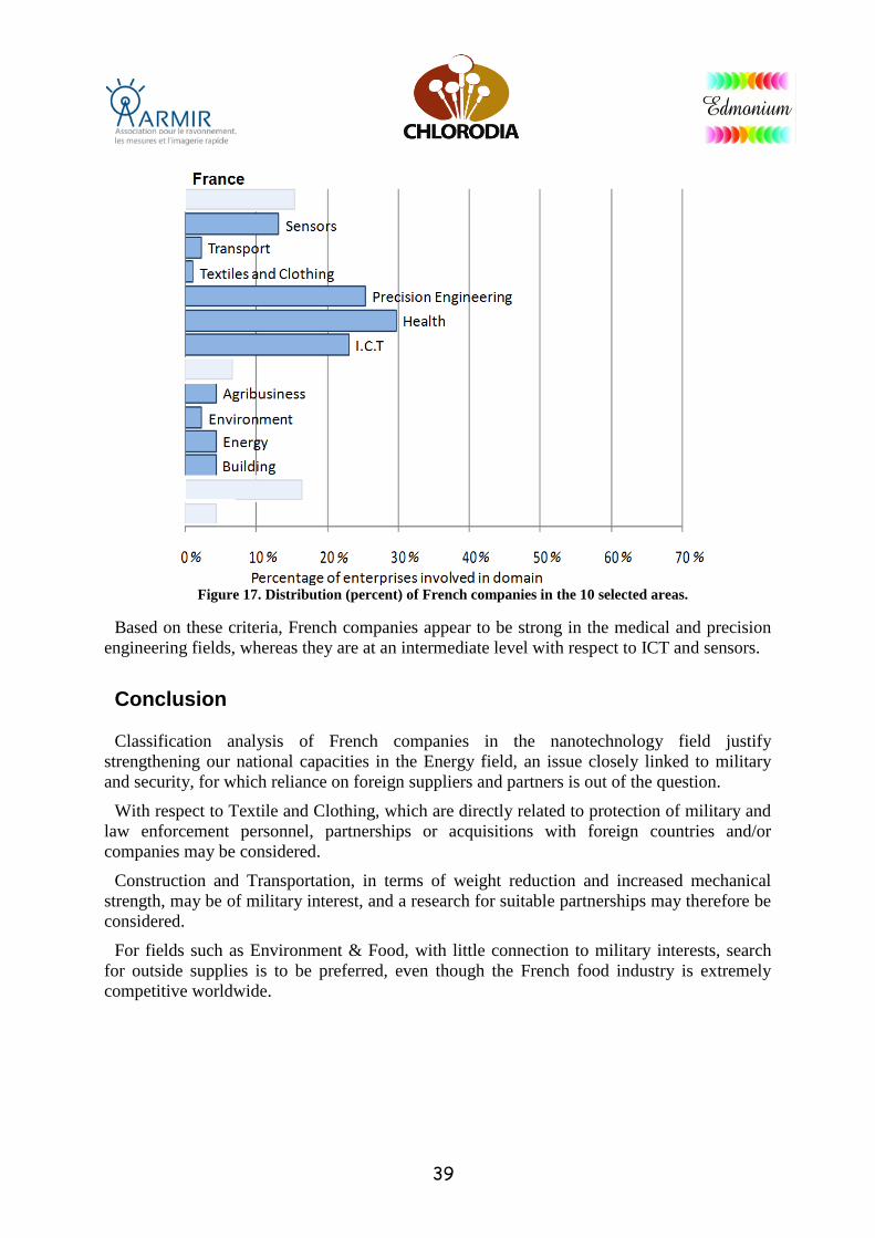
The various activity fields of the 91 French companies are listed below (Figures 16 and 17).
. Figure 16. Distribution of the 91 French companies by field.
French nanotechnology companies are especially numerous in the medical, precision
engineering and information and communications technology fields. Figure 17 shows the
results as a percentage of French companies in the 10 areas identified as potentially related to
military and / or security applications.
39
Figure 17. Distribution (percent) of French companies in the 10 selected areas.
Based on these criteria, French companies appear to be strong in the medical and precision
engineering fields, whereas they are at an intermediate level with respect to ICT and sensors.
Conclusion
Classification analysis of French companies in the nanotechnology field justify
strengthening our national capacities in the Energy field, an issue closely linked to military
and security, for which reliance on foreign suppliers and partners is out of the question.
With respect to Textile and Clothing, which are directly related to protection of military and
law enforcement personnel, partnerships or acquisitions with foreign countries and/or
companies may be considered.
Construction and Transportation, in terms of weight reduction and increased mechanical
strength, may be of military interest, and a research for suitable partnerships may therefore be
considered.
For fields such as Environment & Food, with little connection to military interests, search
for outside supplies is to be preferred, even though the French food industry is extremely
competitive worldwide.
40
IV.3 GERMANY
IV.3.a Data base
Population (2010) 81 millions
Surface area (mainland) 356,026 sq. km
Average population density 230 residents/sq. km
GDP (2010) USD 3,900 billion
GDP per capita (2010) USD 35,900
HDI (2010) 0.885
IV.3.b Germany’s efforts
Germany is the leading investor in Europe in the field of nanotechnologies. Since 1998,
Germany has developed skills centers, made major investments and built significant facilities,
which are available to university as well as non-university research centers. Industry, in
particular SMEs/SMIs, benefit directly from these efforts. Organization of research in
Germany is structured through public/private partnerships, as well as innovation inside private
companies, in order to encourage the development of cooperation between researchers well as
development of synergies between existing agencies.
The German Federal Ministry of Education and Research (BMBF) provides significant
support to nanotechnologies.
In the 70s, biotechnology and microelectronics were among the priority areas for research
and development26
. One decade later, materials and information technology research were
added. In the early 90's, new research in the field of miniaturization and integration of
miniaturized components was also conducted. At the same time, efforts in chemistry were
also made. They contributed to development of targeted products and to self-organizing
principles through combination of individual system components. They contributed to
discovery of new design possibilities in the fields of surface technology and materials. The
challenge, in the 21st century, is to combine these different disciplines.
Nanotechnologies, together with biotechnologies and information technologies, are
considered essential for the next long-term growth cycle. BMBF and VDI Center (Association
of German Engineers) have been aware of the long term importance of nanotechnologies, and
have supported their development for a long time.
Starting in 1998, BMBF has intensified its support to projects, and has set up the necessary
infrastructure through newly-created specialized agencies and skill networks.
26
Germany Science, Nanotechnologies in Germany, Information file for Science and Technology by the
Embassy of France in Germany, Free Publication at the French Embassy in Germany, ISBN 2-907531-05-0,
october 2005.
41
German non-university public research in nanotechnologies is concentrated in four research
institutes: MPG, FhG, HGF, WGL (see Appendix 1: Germany, appendices 1 and 2). These
institutes support a large number of research centers and work groups which also cover major
nanotechnology research. These partners are also integrated into various related research areas
involved and into DFG programs. This initiative was started two years before the USA started
their own national initiative, and four years before the European Union took similar measures
within the 6th Research and Development Framework Program (PCRD).
In the field of nanotechnologies, Germany can rely on top scientists, a widespread research
and development network, and engaged engineers and entrepreneurs. In addition to innovative
companies, government agencies provides significant funding to promote this field and
related stakeholders. Necessary measures are being introduced, such as implementation of
networks, establishment of nanotechnology industrial sectors, renewal of scientific talent and
integration of society in this field. Germany is the nanotechnology leader in Europe, in terms
of dedicated public funding and of number of private companies, research institutes or other
university bodies involved.
In Germany, science policy is directed more towards dissemination of scientific and
technological knowledge, and is part of a decentralization tradition, where Länder enjoy great
autonomy. Science policy, including technology transfer, falls within the jurisdiction of
Länder. Development of university/private industry partnerships is mostly based on local
politics. However, the issue of a need for greater federal involvement arose recently, in
support of BMBF initiatives.
In the field of nanotechnologies, German stakeholders were among the first worldwide to
search for application opportunities through deeper basic research. More than 200 German
companies have already taken advantage of this opportunity for innovation, and
nanotechnology knowledge is part of their main activities. There are currently 900 or 1,000
German nanotechnology companies, which use them more and more to create products,
supply them or as investors27
. For these companies, nanotechnologies are more than a fad.
Rather, they prepare for future developments in potential high-employment areas, such as
electronics, information technology, vehicles and machinery manufacture, chemistry,
pharmacy, optics, medicine, biotechnologies, power generation and construction.
There are also many SMEs in Germany which can be described as pure nanotechnology
companies. Such innovative and flexible companies belong to the value creation channel, and
are a key factor in transferring knowledge from research to industry. SMEs hold key functions
in most high-tech industries.
In addition to supporting conventional research projects, BMBF is increasingly trying to
have the regions (Länder) develop major nanotechnology-related subjects, through strategic
research cooperation, in close collaboration with economic and scientific stakeholders.
Funding is made available for competitive industrial innovation projects which include the
whole value creation chain (leading innovations).
27
Private conversation with a representative of the German Ministry of Defense.
42
IV.3.c Priority Sectors
Intensive talks with industrialists and scientists led to new support of nanotechnologies by
BMBF; as a result, about twenty industry-led cooperation projects, involving more than a
hundred partners, were funded.
Such efforts stand out because of their interdisciplinary nature, with the participation of five
BMBF divisions covering various leading innovative subjects, such as:
NanoChemie (chemistry);
Nanomaterials, in automotive (VanoMobil), in mechanical engineering, in nano-
reinforced and multi-function materials (Hybrids and Ceramics), for example;
NanoLux, development of effective lighting sources from semiconductors;
NanoForLife, providing nanomaterials and nano-biotechnology products for public
health;
NanoFab, for Nano electronics manufacturing processes;
NanoSystems, for micro objects;
Nano-optics/ microelectronics and ITC;
Nano-pharmacy/ cosmetics;
Nanobiotechnologies,
Nanotechnologies for energy engineering;
Nano-robots and artificial muscles;
NanoTecture (architecture, constructions);
NanoTextil (textile applications);
Nano-environment for filtration membranes,
…
In the context of the German government 2020 High-Tech Strategy, BMBF decided in
January 2011 to continue its “Nano-Initiative / 2010 Action Plan” with a 2015 action plan.
The purpose is to achieve safe and sustainable nanotechnology, so as:
to take advantage of its potential in educating and research;to contribute to economic
growth and innovation in Germany;
to take advantage of nanotechnology opportunities in health care;
to reap nanotechnology’s contributions for environment, climate protection and energy
supply;
provide for less energy-consuming mobility while respecting the environment;
use nanotechnology for sustainable agriculture and secure food supply.
43
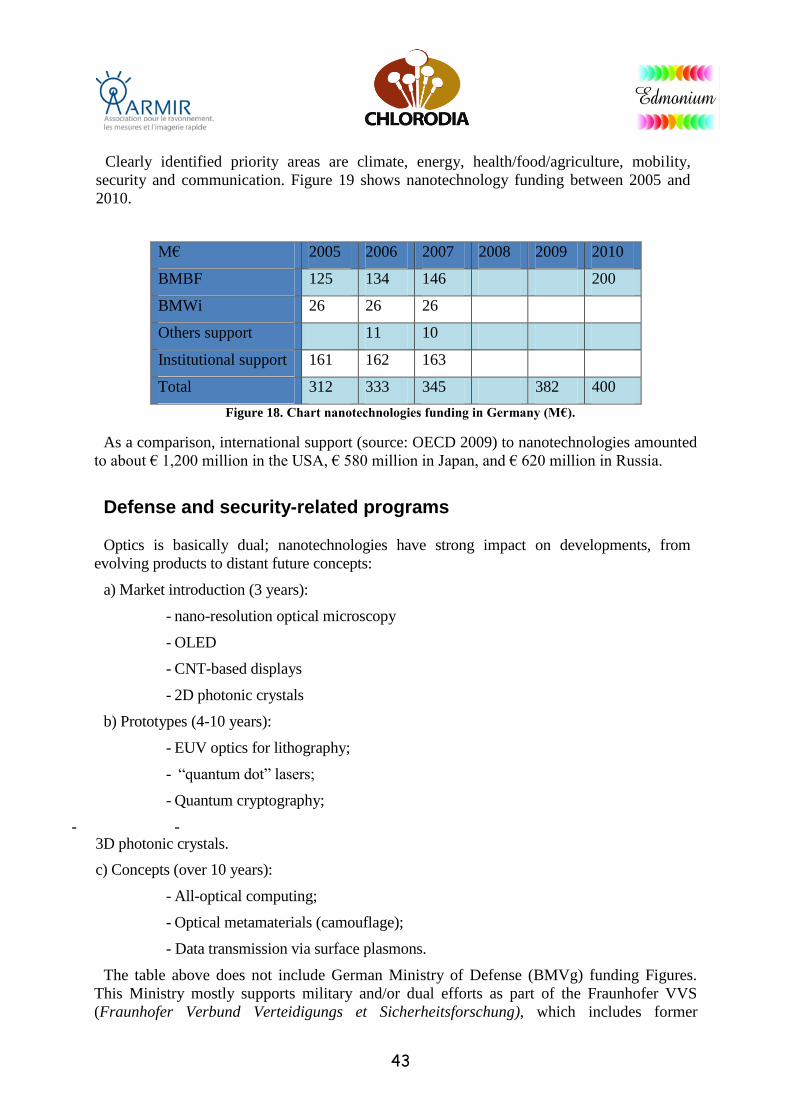
Clearly identified priority areas are climate, energy, health/food/agriculture, mobility,
security and communication. Figure 19 shows nanotechnology funding between 2005 and
2010.
M€ 2005 2006 2007 2008 2009 2010
BMBF 125 134 146 200
BMWi 26 26 26
Others support 11 10
Institutional support 161 162 163
Total 312 333 345 382 400
Figure 18. Chart nanotechnologies funding in Germany (M€).
As a comparison, international support (source: OECD 2009) to nanotechnologies amounted
to about € 1,200 million in the USA, € 580 million in Japan, and € 620 million in Russia.
Defense and security-related programs
Optics is basically dual; nanotechnologies have strong impact on developments, from
evolving products to distant future concepts:
a) Market introduction (3 years):
- nano-resolution optical microscopy
- OLED
- CNT-based displays
- 2D photonic crystals
b) Prototypes (4-10 years):
- EUV optics for lithography;
- “quantum dot” lasers;
- Quantum cryptography;
- - 3D photonic crystals.
c) Concepts (over 10 years):
- All-optical computing;
- Optical metamaterials (camouflage);
- Data transmission via surface plasmons.
The table above does not include German Ministry of Defense (BMVg) funding Figures.
This Ministry mostly supports military and/or dual efforts as part of the Fraunhofer VVS
(Fraunhofer Verbund Verteidigungs et Sicherheitsforschung), which includes former
44
Institutes like Forschungsgesellschaft für Angewandte Naturwissenschaften (FGAN), made
up of the 3 institutes FhG FHR, FhG FKIE and FhG IOSB whose work are mainly of a
military nature.
IV.3.d Evolution of the number of patents
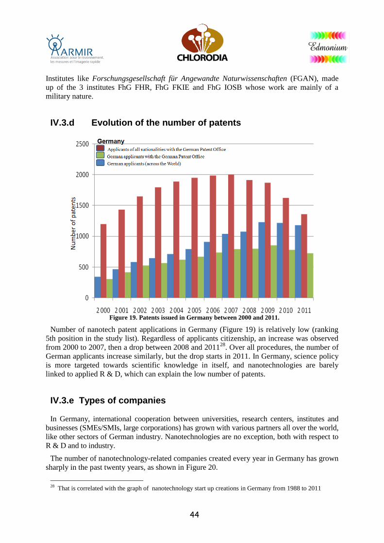
Figure 19. Patents issued in Germany between 2000 and 2011.
Number of nanotech patent applications in Germany (Figure 19) is relatively low (ranking
5th position in the study list). Regardless of applicants citizenship, an increase was observed
from 2000 to 2007, then a drop between 2008 and 201128
. Over all procedures, the number of
German applicants increase similarly, but the drop starts in 2011. In Germany, science policy
is more targeted towards scientific knowledge in itself, and nanotechnologies are barely
linked to applied R & D, which can explain the low number of patents.
IV.3.e Types of companies
In Germany, international cooperation between universities, research centers, institutes and
businesses (SMEs/SMIs, large corporations) has grown with various partners all over the world,
like other sectors of German industry. Nanotechnologies are no exception, both with respect to
R & D and to industry.
The number of nanotechnology-related companies created every year in Germany has grown
sharply in the past twenty years, as shown in Figure 20.
28
That is correlated with the graph of nanotechnology start up creations in Germany from 1988 to 2011
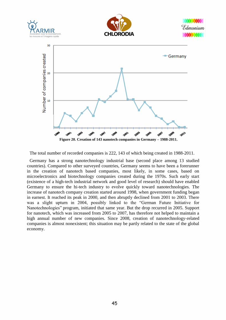
45
Figure 20. Creation of 143 nanotech companies in Germany – 1988-2011.
The total number of recorded companies is 222, 143 of which being created in 1988-2011.
Germany has a strong nanotechnology industrial base (second place among 13 studied
countries). Compared to other surveyed countries, Germany seems to have been a forerunner
in the creation of nanotech based companies, most likely, in some cases, based on
microelectronics and biotechnology companies created during the 1970s. Such early start
(existence of a high-tech industrial network and good level of research) should have enabled
Germany to ensure the hi-tech industry to evolve quickly toward nanotechnologies. The
increase of nanotech company creation started around 1998, when government funding began
in earnest. It reached its peak in 2000, and then abruptly declined from 2001 to 2003. There
was a slight upturn in 2004, possibly linked to the “German Future Initiative for
Nanotechnologies” program, initiated that same year. But the drop recurred in 2005. Support
for nanotech, which was increased from 2005 to 2007, has therefore not helped to maintain a
high annual number of new companies. Since 2008, creation of nanotechnology-related
companies is almost nonexistent; this situation may be partly related to the state of the global
economy.
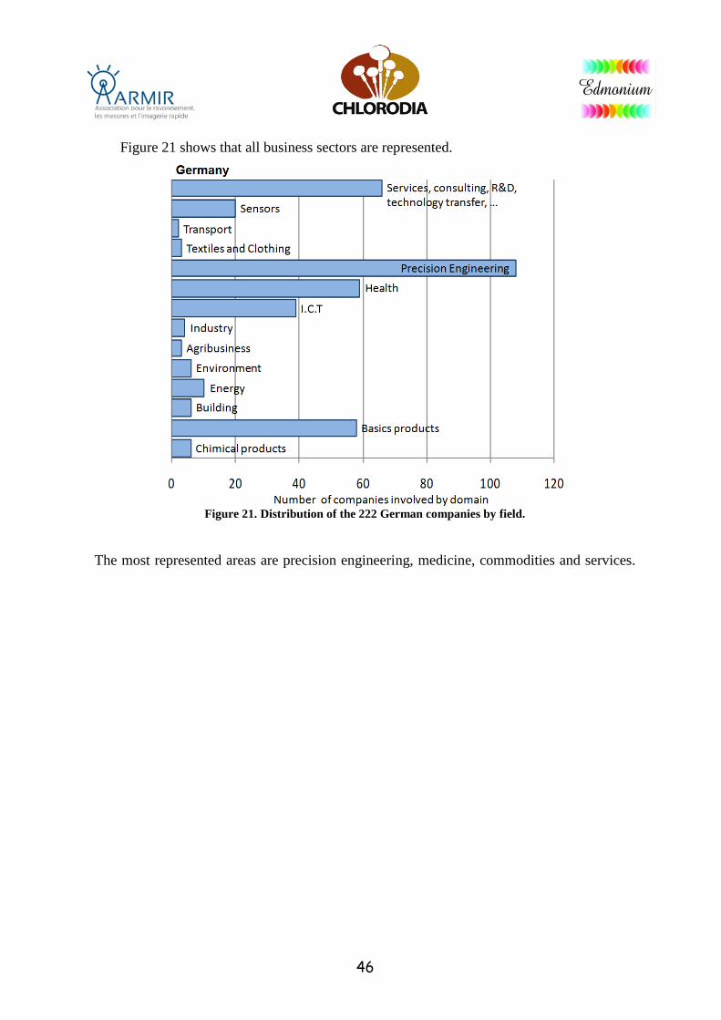
46
Figure 21 shows that all business sectors are represented.
Figure 21. Distribution of the 222 German companies by field.
The most represented areas are precision engineering, medicine, commodities and services.
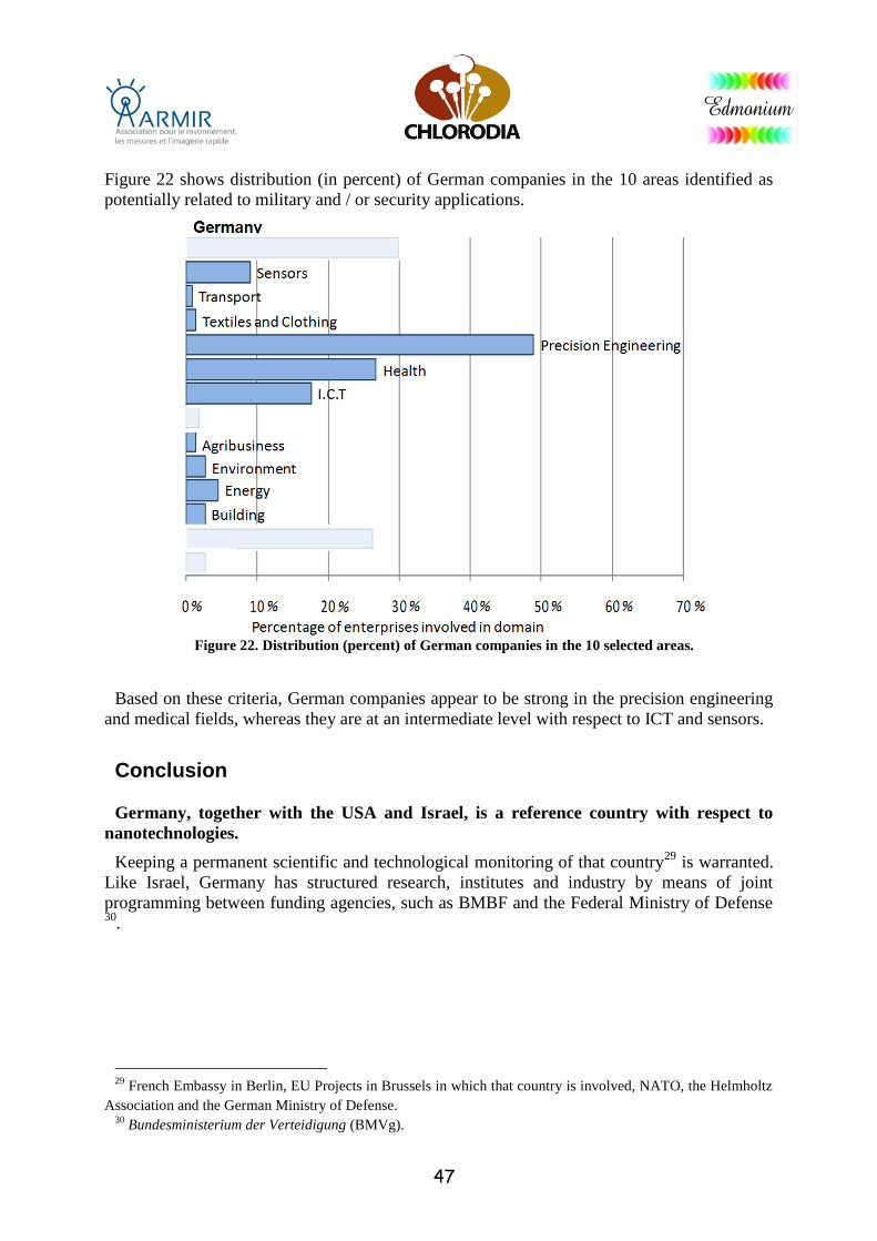
47
Figure 22 shows distribution (in percent) of German companies in the 10 areas identified as
potentially related to military and / or security applications.
Figure 22. Distribution (percent) of German companies in the 10 selected areas.
Based on these criteria, German companies appear to be strong in the precision engineering
and medical fields, whereas they are at an intermediate level with respect to ICT and sensors.
Conclusion
Germany, together with the USA and Israel, is a reference country with respect to
nanotechnologies.
Keeping a permanent scientific and technological monitoring of that country29
is warranted.
Like Israel, Germany has structured research, institutes and industry by means of joint
programming between funding agencies, such as BMBF and the Federal Ministry of Defense 30
.
29
French Embassy in Berlin, EU Projects in Brussels in which that country is involved, NATO, the Helmholtz
Association and the German Ministry of Defense. 30
Bundesministerium der Verteidigung (BMVg).
48
IV.4 BRAZIL
IV.4.a Data base
Population (2011) 192 millions
Area 8 million sq. km
Average density 8,3 residents/sq. km
GDP (2011) USD 2,517 billions
GDP/capita $10,816 $
HDI (2010) 0.813
The Federal Republic of Brazil is a great democracy, politically stable, which has been
among the top ten world economies for more than a decade; However, it also has
characteristics of developing countries. Partly covered by the Amazon, the largest forest basin
in the world, Brazil is one of the wealthiest countries of the world in terms of biodiversity.
Brazil also has significant sources of raw material, such as oil, neodymium (rare earth
elements)31
, etc.
The national Brazilian research and innovation system, SNRI, is young and complicated, but
features a solid architecture (see Appendix 2: Brazil). It is a good quality system, but it suffers
from insufficient human and financial resources, even though significant efforts have been
made in the past ten years.
Brazilian investment in research and technological development has been suffering from
instability due to recurrent economic difficulties. The share of private companies R & D
remains very low.
IV.4.b Brazil’s efforts
Strong government support
National nanotechnology development policy in Brazil began after a conference held in
November 2000 in Brasilia, about trends in nanoscience and nanotechnologies. This major
event was organized by the Political Secretariat, the Ministry of Science & Technology and
the National Scientific Research Council (CNPq). During this meeting, 32 researchers from
different disciplines came to an agreement about the need to create a nanoscience and
nanotechnologies program. In 2001, as a follow-up to this conference, CNPq called for
interdisciplinary and multidisciplinary research projects in order to run Redes Cooperativas de
Pesquisa Bàsica e Applicada en Nanociências e Nanotecnologias (Cooperative Networks for
Basic and Applied Research in Nanoscience’s and Nanotechnologies) in order to create and
consolidate national expertise in this field. Four research networks have been created:
nanostructured materials, molecular and interphase nanotechnology, nanobiotechnologies, and
nano-instruments semiconductors and nanostructured materials network.
31
CECILIA JAMASMIE, $8.4 billion rare earth deposit discovered in Brazil, Mining, 9 avril 2012.
49
In 2002, the Ministry of Science and Technology (MCT) created an institute for nanoscience
in Belo Horizonte as part of the Millennium initiative.
In 2003, when President Luis Inacio da Silva (who was strongly committed to
nanotechnologies) was elected, MCT created a new program, supervised by Dr. Fernando
Galembeck (Professor at the University of Campinas).
Although commitment to nanotechnologies started in 2000, it was only in 2004 that the
government acknowledges this sector as forward looking. The government supports public
research but also public-private cooperation 32
.
In 2005, the four networks installed in 2001 were extended to 10 (see Appendix 2, Figure
77), all connected to Brazil Nano program.
investment was consolidated through MTC’s 2004-2007 Multi-Year Plan. (See Figure 23)
By the end of 2006, 106 research projects were running (50 in research, 46 involving
companies, 5 in international cooperation and 5 about social and environmental impact).
Under the February 2007Biotechnology Development Policy, nanotechnologies and
nanoscience are considered as an important contribution to future technological
developments, with applications in biomaterials, human health, agriculture and industrial
biotechnologies.
Financing Budget
Nanotechnology networks 2001-2003 (CNPq) R$3 million
Millennium Institutes 2001-2004 R$22.5 million
Nanotechnology networks 2003-2004 R$5 million
Sectorial funds 2003-2005 R$6.7 million
Program Development of Nanoscience and Nanotechnology (PPA
2004-2007) 2004-2006
R$8.4 million
Sectorial funds 2004-2006 R$9.1 million
RHAE Innovation 2004-2006 R$7.1 million
National Nanotechnology program 2005-2009 R$58.6 million
Millennium institutes and microelectronics call 2005-2008 R$ 21.5 million
National nanotechnology program call 2006 R$28.4 million
2001-2006 Total R$170.2 million
(€61.6 millions)
Figure 23. R&D funding in Brazil.
32
However, publication as original author is predominantly from academia: 78,4%, Government: 5% private
industry: 0.2% Public Industry: 0.8%, Hospital: 0.1, (other being the foreign authors of publications).
Nanotechnology in Latia America, Luiciano Kay, 2006.
50
Nanotechnology research centers in Brazil There is no central point where Brazilian research in Nanotechnologies is concentrated.
However, some cities can be considered as network nodes. The Brazilian government has
made investments in nanotechnology research facilities, such as the LNLS synchrotron, the
Inmetro metrology institute, the CBPF physics research center and the EMBRAPA Center for
Agricultural Research. (Appendix 2, Figure 79).
IV.4.c Priority Sectors Brazil work on a number of industrial application areas such as aerospace, agro-industry,
cosmetics and health care, energy, environment and textiles. Brazil has acquired knowledge
in: nanotechnology, nanobiostructures, nanophotonics, molecular nanotechnology,
nanobiomagnetism, nanoscience, nanocoatings, simulation and modelization,
nanocosmetics, nanoglicobiotechnology. However, publishing activity is focused on 33
:
Physics: 44.5%
Chemistry: 22.3%
Materials Science: 32%
Engineering: 7.1%
Medicine: 5.7%
Biology: 4.9%
Electronics: 4.5%
….
Law
The issue of ethical, social and risks associated with the use of nanotechnologies emerged in
2004, in particular through creation of the Brazilian Nanotechnology, Society and
Environment Network Foundation. Brazilian scientists had introduced nanotechnologies as a
revolutionary area with a huge market potential. To avoid being left behind in the
international race, social impacts and risk had been dismissed so they could not cast a shadow
over an optimistic view of the future of nanotechnologies. A public debate was organized, but
it split the country. Concerns of NGOs and social scientists include risks to short-term health,
and environmental impact. They also consider that the priorities of nanotechnology research
are not appropriate for societal needs.
The need to analyze ethical implications and social impacts derived from dissemination of
nanotechnology products is part of the public document of the Ministry of Science and
Technology 2007 to 2010 action plan (in which nanotechnologies play an important role).
33
Nanotechnology in Latia America, Luiciano Kay, 2006.
51
IV.4.d Brazil on the worldwide stage
Collaboration in R&D
Brazilian scientific work is well internationalized. With 40.3% of international co-
publications (including 31.7% with the United States, 10% with France and 9.5% with the
UK, etc.) in its publications in 2001, Brazil is at the same level as France or Canada based on
this criteria, and ten points above China
In 1992, the EU and Brazil have entered into a framework cooperation agreement and, in
2004, a technological cooperation agreement. A strategy paper has been established for 2007-
2013. That strategy governs development cooperation activities, and has a € 61 million
budget. Priorities defined are:
- To increase exchanges, contacts and knowledge transfer how between the European
Community and Brazil: To support sector-related dialogues; To use higher education
program (€ 30.5 million) to strengthen links between the European Union and
Brazilian academic communities; To create an Institute of European Studies in Brazil.
- To support environmental and sustainable development projects in Brazil.
The EU wants to stimulate research collaborations between European and Latin American
nanotechnology researchers via the 7th
PCRD.
Many R & D partnerships are with bordering countries. Indeed, Argentine RCBC center of
nanotechnology is in Porto Alegre. It is very active in promoting development of human
resources in both countries. There are also:
- A Brazilian-Mexican virtual nanotechnology center, designed to finance collaborative
projects between those countries.A virtual nanotechnology center: “Centro Brasileiro
de Nanociencia Argentino y Nanotecnologia” (CABNN), which uses the facilities of
both countries to develop joint projects, increase human resources, and exchanges.
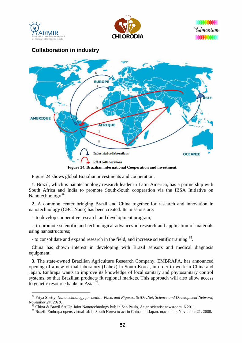
52
Collaboration in industry
Figure 24. Brazilian international Cooperation and investment.
Figure 24 shows global Brazilian investments and cooperation.
1. Brazil, which is nanotechnology research leader in Latin America, has a partnership with
South Africa and India to promote South-South cooperation via the IBSA Initiative on
Nanotechnology34
.
2. A common center bringing Brazil and China together for research and innovation in
nanotechnology (CBC-Nano) has been created. Its missions are:
- to develop cooperative research and development program;
- to promote scientific and technological advances in research and application of materials
using nanostructures;
- to consolidate and expand research in the field, and increase scientific training 35
.
China has shown interest in developing with Brazil sensors and medical diagnosis
equipment.
3. The state-owned Brazilian Agriculture Research Company, EMBRAPA, has announced
opening of a new virtual laboratory (Labex) in South Korea, in order to work in China and
Japan. Embrapa wants to improve its knowledge of local sanitary and phytosanitary control
systems, so that Brazilian products fit regional markets. This approach will also allow access
to genetic resource banks in Asia 36
.
34
Priya Shetty, Nanotechnology for health: Facts and Figures, SciDevNet, Science and Development Network,
November 24, 2010. 35
China & Brazil Set Up Joint Nanotechnology hub in Sao Paulo, Asian scientist newsroom, 6 2011. 36
Brazil: Embrapa opens virtual lab in South Korea to act in China and Japan, macauhub, November 21, 2008.

53
4. A Brazil-UK collaboration, within the framework of a bioscience innovation network, to
enable knowledge transfer and promote interaction of Biosciences KTN members with part of
Brazil investment community. This network will act as venture-capital in Brazil, and will
have direct access to UK companies that are well-matched to the Brazilian biotechnology
markets and the member firms that might be interested in seeking financing and / or
collaboration in Brazil.
5. Within the framework of Brazil-Portugal cooperation, a nanotechnology workshop took
place at PFBC (Brazilian Physics Research Center of the Ministry of Science and
Technology, in Rio de Janeiro) as part of the Protocol between Portugal’s Ministry of
Science, Technology and Higher Education, and of Brazil’s Ministry of Science and
Technology37
.
6. Costa Rica and Brazil cooperate in the nanotechnology and aerospace engineering
fields38
.
It is notable that collaborations identified in this study are highly focused on R&D.
37
1st Brazil-Portugal International Cooperation in Nanotechnology Workshop, UMIC, Ministry of education
and science, july 17, 2010. 38
Costa Rica & Brazil Cooperate in Nanotechnology & Aerospace Engineering, MICITI, Ministerio de ciencia
y tecnologia, November 23, 2010.
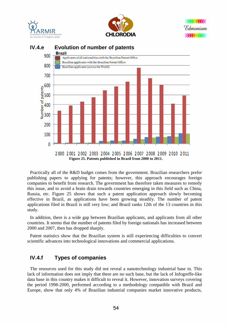
54
IV.4.e Evolution of number of patents
Figure 25. Patents published in Brazil from 2000 to 2011.
Practically all of the R&D budget comes from the government. Brazilian researchers prefer
publishing papers to applying for patents; however, this approach encourages foreign
companies to benefit from research. The government has therefore taken measures to remedy
this issue, and to avoid a brain drain towards countries emerging in this field such as China,
Russia, etc. Figure 25 shows that such a patent application approach slowly becoming
effective in Brazil, as applications have been growing steadily. The number of patent
applications filed in Brazil is still very low; and Brazil ranks 12th of the 13 countries in this
study.
In addition, there is a wide gap between Brazilian applicants, and applicants from all other
countries. It seems that the number of patents filed by foreign nationals has increased between
2000 and 2007, then has dropped sharply.
Patent statistics show that the Brazilian system is still experiencing difficulties to convert
scientific advances into technological innovations and commercial applications.
IV.4.f Types of companies
The resources used for this study did not reveal a nanotechnology industrial base in. This
lack of information does not imply that there are no such base, but the lack of Infogreffe-like
data base in this country makes it difficult to reveal it. However, innovation surveys covering
the period 1998-2000, performed according to a methodology compatible with Brazil and
Europe, show that only 4% of Brazilian industrial companies market innovative products,
55
compared to 18% in France39
. This survey is consistent with the results obtained, which
suggest that commercialization of public research is low. In addition, public research occurs
prior to product development, and therefore not really in phase with industry. I tis hoped that,
a few years from now, knowledge acquired will be converted into marketable products.
Conclusion
Brazil has followed the international trend since 2000 by focusing on nanotechnologies. The
nanotechnology and nanoscience policy started during Fernando Henrique Cardoso's
administration (1999 to 2002) was designed to create a Nanotechnology Reference Center
linked to MCT. This center had a dual mission: stimulating university research and
encouraging the use of new technologies in the private sector. In terms of the number of
publications and patents, Brazil is nanotechnology leader in the South American region
(Argentina, Uruguay, and Chile)40
. Despite Brazilian multidisciplinary programs, most
publications are concentrated on physics, chemistry and materials science.
Although such a policy, pursued by Lula, has created many nanotechnology research centers
and international cooperation, a real industrial fabric has, however, not emerged. It is
therefore critical for Brazil to acquire institutions in order to facilitate the transfer of
technology.
The possibilities for upgrading and optimizing bilateral cooperation, without increase in
funding, should take into account scientific priorities announced by French and Brazilian
authorities, both of which are focused on development of innovation and technology transfer,
essential to competitiveness.
Brazil does not seem to be a key industrial partner for France, but might be a candidate for
interesting nanotechnology research collaborations.
39
Brazilian Scientists Embrace Nanotechnologies, Invernizzi, Noela, RELANS, 2007. 40
The Universities of Sao Paulo and Campinas account alone 34 percent of the South American publications.

56
IV.5 China
IV.5.a Data base
Population (2011) 1.34 billions
Area 9.6 million sq. km
Average Density 140 residents/sq. km
GDP (2011) USD 7,000 billion
GDP/capita $5,200
HDI (2009) 0.77
IV.5.b China’s efforts 41
The Popular Republic of China considers nanoscience and nanotechnologies (NST) as the
way for the future, especially in economic terms, and has implemented a number of programs
to develop this sector.
In 2006, the Chinese government launched, via the Business Council, a long-term national
plan (2006 to 2020) devoted to scientific and technological development of the country where
NST were taking a growing place.
A proactive research, industrialization and marketing policy for products and technologies
started, amplifying the effort that had existed since the 2000s
Very significant funds were allocated by the State for several R & D programs, including the
National Research Plan, plan 863 and plan 973. Investments amounted to approximately 760
million dollars from 2006 to 2010, an increase of nearly 300% over the period from 2001 to 2005.
NST publications and patent applications grew very rapidly from 2000 to 2010, reflecting
the importance of government support and the attractiveness of new topics for researchers.
(See Figure 26)
China currently ranks first worldwide with respect to number of nanotechnology patents
filed, having surpassed the United States since 2010.
The country appears to have currently more than 350 universities, around thirty research
institutes and over 400 companies involved in the NST, with a global workforce of
41
ALAIN DE NIEVE, Panorama of programs and investments in nanotechnology, Agoravox, October 20,
2009.
JIM WANG, Development of nanotechnology in China, Association China Nanotech.
ZOE LOMBARD, Balance from the XIth Five Year Plan for nanosciences, China is developing its own nano-
object standardization device BE China No. 100, January 28, 2011.
China’s Program for Science and Technology Modernization: Implications for American Competitiveness,
U.S.-China economic and security review commission, CENTRA Technology, Inc, Micah Springut, Stephen
Schlaikjer, janvier 2011.
Military, Arms Control, and Security Aspects of Nanotechnology, Jürgen Altmann and Mark A. Gubrud,
Institut für Experimentalphysik, Universität Dortmund, 2004.
57
approximately 26,000 researchers. The government is also investing heavily in industrializing
research, and is facilitating the commercialization of products derived thereof 42
.
In the north, the Beijing National Centre for Nanoscience’s.
In the northeast, the National nanotechnologies Research Institute and Tianjin
Engineering.
In the south, the National Applied Nanotechnologies and Engineering Center in
Shanghai.
The Beijing Nanoscience’s National Center includes a large number of academies,
universities and institutions: the Chinese Academy of Sciences, the Institute for Research on
iron and steel for China, the Polytechnic University Beijing, the Academy for building
materials of Pekin, Peking University, Pekin University of Technology, Tsinghua University,
Technological University of Chemistry, Tianjin University, Nankai University and those of
Jilin.
The Shanghai National Center mainly brings together: the Chinese Academy of Sciences,
University of Science and Technology of China, the Technology University of East China, the
Institute of Physics and Technology in Shanghai, the Shanghai Jiaotong University, Fudan
University, Tongji University, Zhejiang University, Nanjing University and the one of
Shandong.
These two centers represent 80% of the country NST activity.
42
A convincing example is the International nanotechnologies Innovation Park in Suzhou, which has more than
doubled its sales from 2008 to 2009, with a profit of nearly $ 400 million in 2009 and a similar level of growth in
2010.
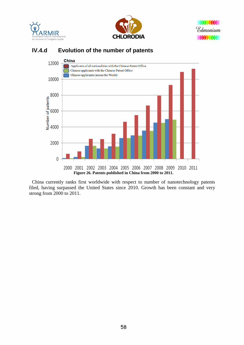
58
IV.4.d Evolution of the number of patents
Figure 26. Patents published in China from 2000 to 2011.
China currently ranks first worldwide with respect to number of nanotechnology patents
filed, having surpassed the United States since 2010. Growth has been constant and very
strong from 2000 to 2011.
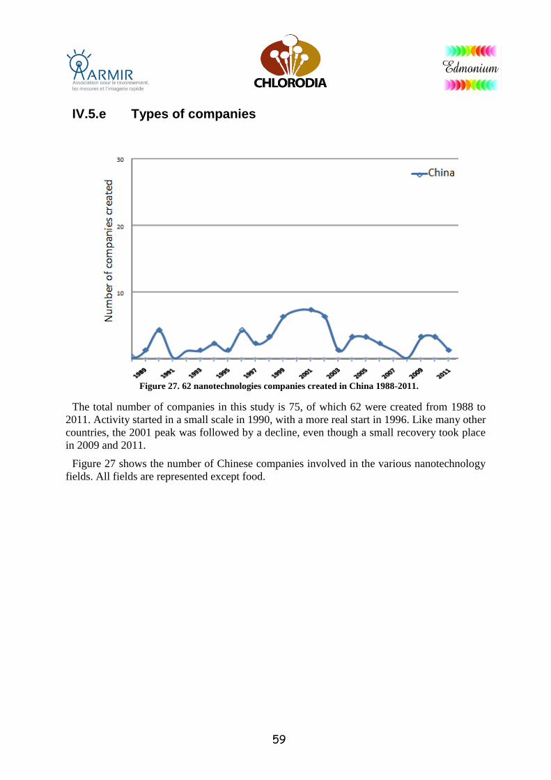
59
IV.5.e Types of companies
Figure 27. 62 nanotechnologies companies created in China 1988-2011.
The total number of companies in this study is 75, of which 62 were created from 1988 to
2011. Activity started in a small scale in 1990, with a more real start in 1996. Like many other
countries, the 2001 peak was followed by a decline, even though a small recovery took place
in 2009 and 2011.
Figure 27 shows the number of Chinese companies involved in the various nanotechnology
fields. All fields are represented except food.
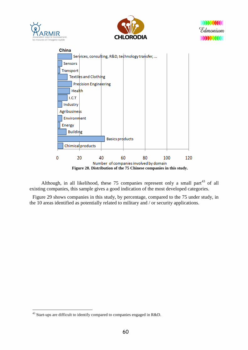
60
Figure 28. Distribution of the 75 Chinese companies in this study.
Although, in all likelihood, these 75 companies represent only a small part43
of all
existing companies, this sample gives a good indication of the most developed categories.
Figure 29 shows companies in this study, by percentage, compared to the 75 under study, in
the 10 areas identified as potentially related to military and / or security applications.
43
Start-ups are difficult to identify compared to companies engaged in R&D.
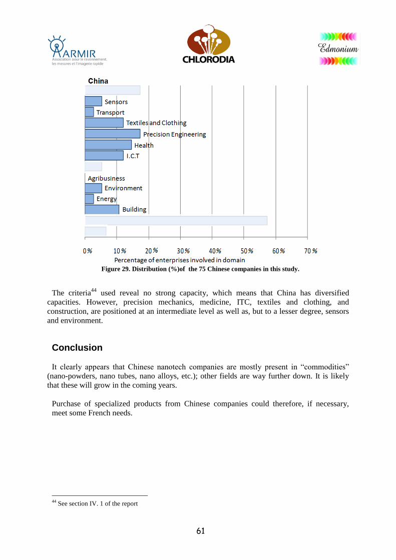
61
Figure 29. Distribution (%)of the 75 Chinese companies in this study.
The criteria44
used reveal no strong capacity, which means that China has diversified
capacities. However, precision mechanics, medicine, ITC, textiles and clothing, and
construction, are positioned at an intermediate level as well as, but to a lesser degree, sensors
and environment.
Conclusion
It clearly appears that Chinese nanotech companies are mostly present in “commodities”
(nano-powders, nano tubes, nano alloys, etc.); other fields are way further down. It is likely
that these will grow in the coming years.
Purchase of specialized products from Chinese companies could therefore, if necessary,
meet some French needs.
44
See section IV. 1 of the report
62
IV.6. South Korea
IV.6.a Data base
Population (2011) 48,754 millions
Area 99,274 sq. km
Average density 488 residents/sq. km
GDP (2011) $1.356 billions
GDP/capita (2011) $27,813
HDI (2011) 0.897
IV.6.b Korea’s efforts
The Republic of Korea spends, for its R&D programs devoted to nanoscience and
nanotechnology, significant amounts: about 3.5% of the GDP. This R&D effort is organized
around co-financed Public-Private Partnerships. The country is committed to a third phase of
industrial development, following the two initial phases, based respectively on development
of light industries, then on heavy and mechanical industries. Priority is now given to sectors
deemed to be the way of the future, including development of Services45
. A recently-
implemented decentralization policy is designed to develop regional poles in a still highly
centralized state (see Appendix 3: South Korea, Appendix 1). Korea also has a policy of
active international collaboration designed to improve skills in state-of-the-art technological
fields46
.
Founded in 1999, the National Science and Technology Council (NTSC) defines priorities,
and is responsible for coordinating effectively countrywide Science and Technology policies
and R&D programs. Chaired by the President of the Republic, it is made up of scientists and
technological government ministers, and representatives of academia and industry. (see
Appendix 3: South Korea, Appendix 2)
South Korea ranks 4th among the 15 most important global nanotechnology research centers
(see Figure 30).
45
Statistical Yearbook of Education 2011, MEST and Ministry of Education, Science and Technology:
http://www.mest.go.kr 46
Research and Technology in South Korea, Scientific Section of the Embassy of France, in September 2009.
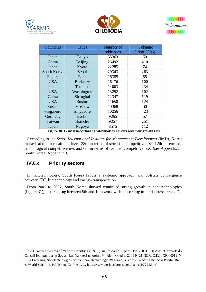
63
Countries Cities Number of
addresses
% change
(1998-2006)
Japan Tokyo 35363 69
China Beijing 26492 410
Japan Kyoto 22285 74
South Korea Seoul 20343 263
France Paris 16385 55
USA Berkeley 16176 100
Japan Tsukuba 14003 234
USA Washington 13292 102
China Shanghai 12347 519
USA Boston 11650 124
Russia Moscow 10368 60
Singapore Singapore 10256 423
Germany Berlin 9065 57
Taiwan Hsinchu 9057 251
Japan Nagoya 8575 112 Figure 30. 15 most important nanotechnology clusters and their growth rate.
According to the Swiss International Institute for Management Development (IMD), Korea
ranked, at the international level, 38th in terms of scientific competitiveness, 12th in terms of
technological competitiveness and 6th in terms of national competitiveness. (see Appendix 3:
South Korea, Appendix 3).
IV.6.c Priority sectors
In nanotechnology, South Korea favors a systemic approach, and bolsters convergence
between ITC, biotechnology and energy-transportation.
From 2005 to 2007, South Korea showed continued strong growth in nanotechnologies
(Figure 31), thus ranking between 5th and 10th worldwide, according to market researches. 47
.
47
A) Competitiveness of Various Countries in NT, (Lux Research Report, Dec. 2007) – B) Avis et rapports du
Conseil Economique et Social: Les Nanotechnologies, M. Alain Obadia, 2008 N°21 NOR: C.E.S. X08000121V
– C) Emerging Nanotechnologies power - Nanotechnology R&D and Business Trends in the Asia Pacific Rim,
© World Scientific Publishing Co. Pte. Ltd., http://www.worldscibooks.com/nanosci/7224.html
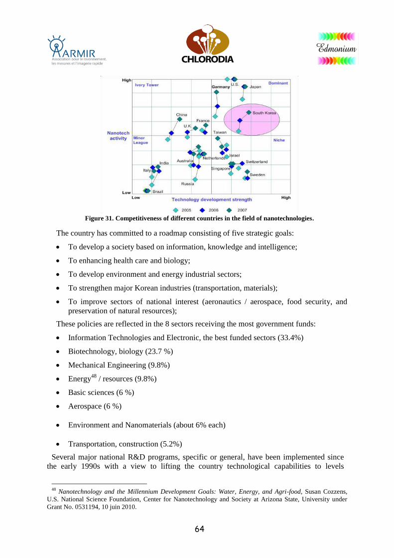
64
Figure 31. Competitiveness of different countries in the field of nanotechnologies.
The country has committed to a roadmap consisting of five strategic goals:
To develop a society based on information, knowledge and intelligence;
To enhancing health care and biology;
To develop environment and energy industrial sectors;
To strengthen major Korean industries (transportation, materials);
To improve sectors of national interest (aeronautics / aerospace, food security, and
preservation of natural resources);
These policies are reflected in the 8 sectors receiving the most government funds:
Information Technologies and Electronic, the best funded sectors (33.4%)
Biotechnology, biology (23.7 %)
Mechanical Engineering (9.8%)
Energy48
/ resources (9.8%)
Basic sciences (6 %)
Aerospace (6 %)
Environment and Nanomaterials (about 6% each)
Transportation, construction (5.2%)
Several major national R&D programs, specific or general, have been implemented since
the early 1990s with a view to lifting the country technological capabilities to levels
48
Nanotechnology and the Millennium Development Goals: Water, Energy, and Agri-food, Susan Cozzens,
U.S. National Science Foundation, Center for Nanotechnology and Society at Arizona State, University under
Grant No. 0531194, 10 juin 2010.
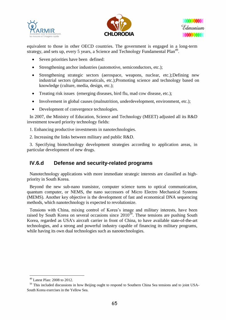
65
equivalent to those in other OECD countries. The government is engaged in a long-term
strategy, and sets up, every 5 years, a Science and Technology Fundamental Plan49
.
Seven priorities have been defined:
Strengthening anchor industries (automotive, semiconductors, etc.);
Strengthening strategic sectors (aerospace, weapons, nuclear, etc.);Defining new
industrial sectors (pharmaceuticals, etc.);Promoting science and technology based on
knowledge (culture, media, design, etc.);
Treating risk issues (emerging diseases, bird flu, mad cow disease, etc.);
Involvement in global causes (malnutrition, underdevelopment, environment, etc.);
Development of convergence technologies.
In 2007, the Ministry of Education, Science and Technology (MEET) adjusted all its R&D
investment toward priority technology fields:
1. Enhancing productive investments in nanotechnologies.
2. Increasing the links between military and public R&D.
3. Specifying biotechnology development strategies according to application areas, in
particular development of new drugs.
IV.6.d Defense and security-related programs
Nanotechnology applications with more immediate strategic interests are classified as high-
priority in South Korea.
Beyond the new sub-nano transistor, computer science turns to optical communication,
quantum computer, or NEMS, the nano successors of Micro Electro Mechanical Systems
(MEMS). Another key objective is the development of fast and economical DNA sequencing
methods, which nanotechnology is expected to revolutionize.
Tensions with China, mixing control of Korea’s image and military interests, have been
raised by South Korea on several occasions since 201050
. These tensions are pushing South
Korea, regarded as USA's aircraft carrier in front of China, to have available state-of-the-art
technologies, and a strong and powerful industry capable of financing its military programs,
while having its own dual technologies such as nanotechnologies.
49
Latest Plan: 2008 to 2012. 50
This included discussions in how Beijing ought to respond to Southern China Sea tensions and to joint USA-
South Korea exercises in the Yellow Sea.
66
IV.6.e Evolution of the numbers of patents
Figure 32. Patents published in South Korea between 2000 and 2011.
In terms of patent filing, South Korea's performance is impressive, as evidenced by his 4th
place out of the considered 13 countries. There has been a steady growth from 2000 to 2010
(Figure 32).
IV.6.f Types of companies
South Korea is actively collaborating in R & D, in particular with the three following
countries:
France: the framework of the France / South Korea Science and Technology
cooperation system helps to pay for exchanging researchers working on some thirty
projects, jointly selected by both parties on scientific criteria.
It is an exchange tool, designed for networking scientists rather than collaborative
research. Management of the program is entrusted to the National Research Foundation
for Korea, and the Embassy of France in Korea for France. In addition, several Korean
teams are financed by multilateral programs of the French Ministry of Foreign Affairs,
in the context of Franco-Asian research projects in the field of I.C.T51
.
China: selected cooperation topics are weather forecasting, biotechnologies, new
materials, environmental technologies, applied laser technologies, and the
commercialization of advanced technologies. The two countries have created 4 joint
research centers in Korea and 2 in China. Great Britain: South Korea signed with Great
51
STIC-Asia Program.
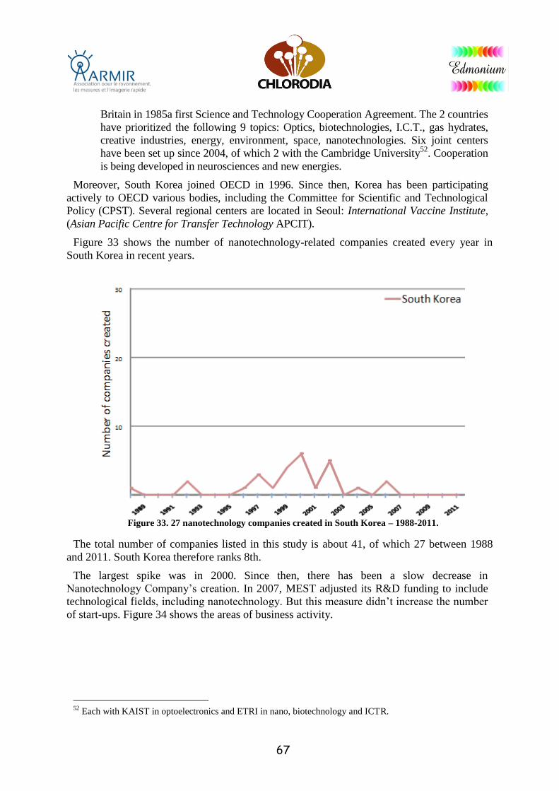
67
Britain in 1985a first Science and Technology Cooperation Agreement. The 2 countries
have prioritized the following 9 topics: Optics, biotechnologies, I.C.T., gas hydrates,
creative industries, energy, environment, space, nanotechnologies. Six joint centers
have been set up since 2004, of which 2 with the Cambridge University52
. Cooperation
is being developed in neurosciences and new energies.
Moreover, South Korea joined OECD in 1996. Since then, Korea has been participating
actively to OECD various bodies, including the Committee for Scientific and Technological
Policy (CPST). Several regional centers are located in Seoul: International Vaccine Institute,
(Asian Pacific Centre for Transfer Technology APCIT).
Figure 33 shows the number of nanotechnology-related companies created every year in
South Korea in recent years.
Figure 33. 27 nanotechnology companies created in South Korea – 1988-2011.
The total number of companies listed in this study is about 41, of which 27 between 1988
and 2011. South Korea therefore ranks 8th.
The largest spike was in 2000. Since then, there has been a slow decrease in
Nanotechnology Company’s creation. In 2007, MEST adjusted its R&D funding to include
technological fields, including nanotechnology. But this measure didn’t increase the number
of start-ups. Figure 34 shows the areas of business activity.
52
Each with KAIST in optoelectronics and ETRI in nano, biotechnology and ICTR.
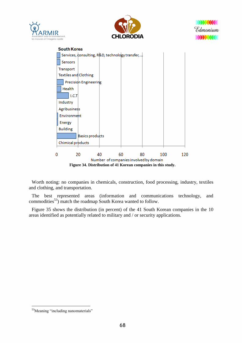
68
Figure 34. Distribution of 41 Korean companies in this study.
Worth noting: no companies in chemicals, construction, food processing, industry, textiles
and clothing, and transportation.
The best represented areas (information and communications technology, and
commodities53
) match the roadmap South Korea wanted to follow.
Figure 35 shows the distribution (in percent) of the 41 South Korean companies in the 10
areas identified as potentially related to military and / or security applications.
53
Meaning “including nanomaterials”
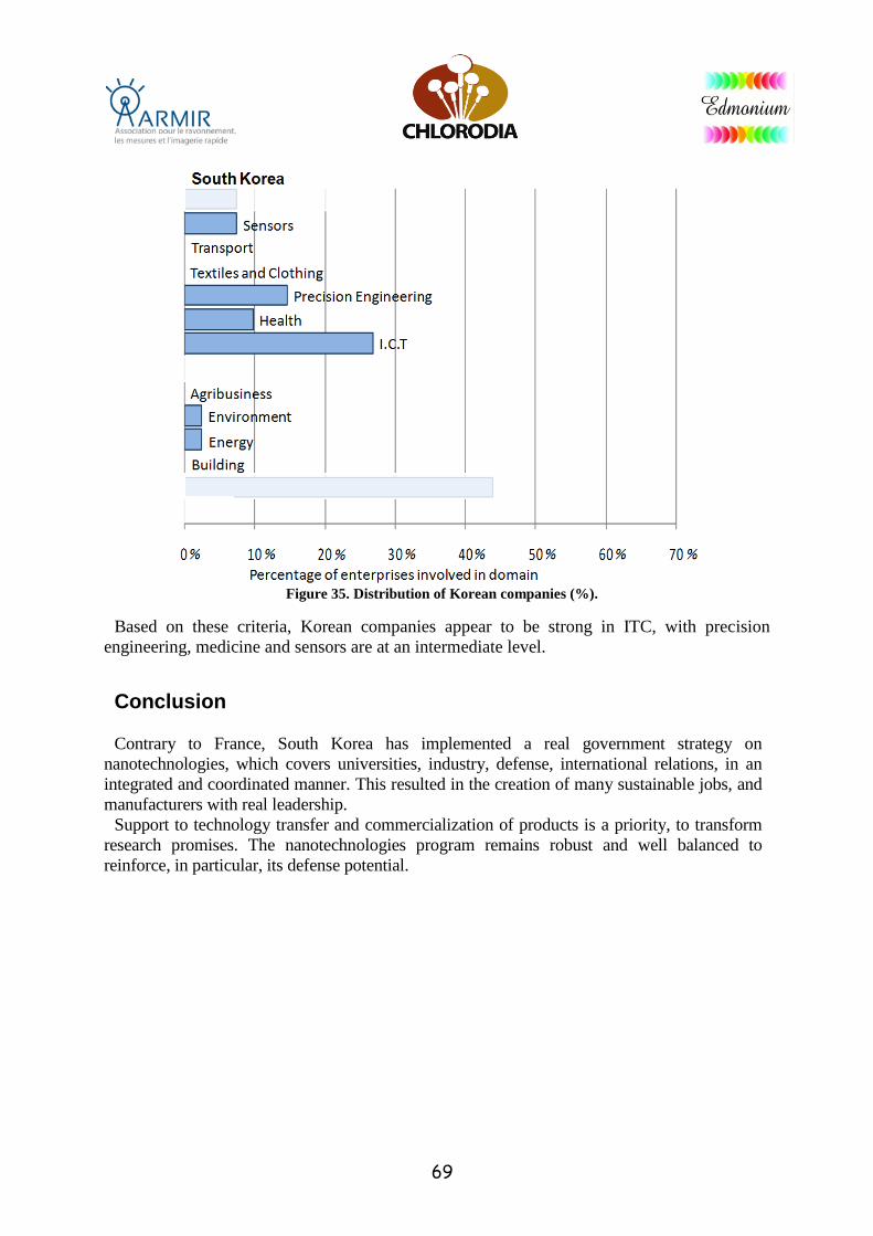
69
Figure 35. Distribution of Korean companies (%).
Based on these criteria, Korean companies appear to be strong in ITC, with precision
engineering, medicine and sensors are at an intermediate level.
Conclusion
Contrary to France, South Korea has implemented a real government strategy on
nanotechnologies, which covers universities, industry, defense, international relations, in an
integrated and coordinated manner. This resulted in the creation of many sustainable jobs, and
manufacturers with real leadership.
Support to technology transfer and commercialization of products is a priority, to transform
research promises. The nanotechnologies program remains robust and well balanced to
reinforce, in particular, its defense potential.
70
IV.7 United States
IV.7.a Database
Population (2012) 313 millions
Area 7,700,000 sq. km
Average Density 33.7 residents/sq. km
GDP (2011) $15,094 billion
GDP/capital (2012) $48 386
HDI (2012) 0.910
IV.7.b USA’s efforts
Nanoscience’s and nanotechnologies programs (NST)
In the late 90s, US think tanks54
were beginning to see the possibilities of an emerging field,
i.e. nanotechnologies. Their development was going to collide with the administrative
division of federal agencies specialized in R&D financing. Comprehension and mastery of
new phenomena and properties at the nanoscale did not just revolutionize one area - materials
science, energy, information technologies, health, etc. - in particular, but all of them.
Development of nanoscience, therefore, called for a wide financing program that, rather than
being built independently by each agency, required all of them to come together. The solution
found was a federal nanotechnology financing coordination program; created in late 2000
under the name National Nanotechnology Initiative (NNI). Within the NNI, strategic plans are
updated every 3 years, to make available new tools to ensure better coordination,
communication and cooperation among federal agencies. NNI has no authority over these
agencies, who can freely decide their research programs. NNI’s budget has been multiplied by
5 in 10 years, to around $ 2.1 billion for 2012. With $ 14 billion invested, NNI is now the
largest US federal R&D financing program since the space program. Research infrastructures
implemented by NNI provides a solid foundation upon which the US intend to capitalize in
order to maintain their global leadership in the next decade55
. NNI has always been supported
by the White House and Congress. It survived three administrations (Clinton, Bush
and Obama) and 6 Congresses. Such support, reinforced by positive feedback, has secured its
very strong budget growth.
For NNI, the year 2010 was characterized by validation of its strategic plan (3rd version)
and that of the EHS (Environment, Health, Security) second phase.
54
A think tank, or laboratory of ideas, is a private institution, in principle independent of political parties, non-
profit, which brings together experts and produces studies and proposals in the field of public policy. 55
Dix ans de Nanotechnologies aux Etats-Unis – Histoire, bilan et perspectives du programme National
Nanotechnology Initiative, Vincent Reillon, Rapport d’Ambassade de France à Washington, Agence pour la
Diffusion de l'Information Technologique, avril 2011.
71
The roadmap for the next ten years has designated energy as the principal field, along with
health care, electronics and national defense. Cooperation is being developed in the field of
neurosciences and new energies. Mass-producing standardized nanomaterials in a
responsible way is the challenge for 2020 (see Appendix 4: United States, Appendix 1).
IV.7.c Priority Sectors
Nanoscience’s bear the promise of radical transformation in many areas: energy, health care,
information technology, material sciences. The great challenges listed by the NNI are:
Nanostructured materials by design;
Nanoelectronics, optoelectronics and magnetism; Advanced medical care:
Therapeutic and diagnosis;
Improvement of the environment;Energy conversion and efficient storage;
Space exploration;
Biosensors for therapies and detection of biological threats;
Economical and safe transportation; Nano-systems (nano-robots, NAVs56
: Nano
Air Vehicle);
National security.
Figure 36 shows the evolution of the budget dedicated to the NNI for the main agencies. The
4 NNI topmost agencies are: DoD, NSF, DoE and NIH, accounting for 90% of the budget by
themselves. The DoE budget is still growing strongly, the energy being a priority of the
Obama administration. NASA’S budget was relatively high from 2001 to 2006; although
budgets have been increasing again, they have not reached to their previous level.
See Appendix 4: United States, Appendix 2
56
Nano Air Vehicles, a Technology Forecast, William A. Davis, Major, USAF, Center for Strategy and
Technology, Air War College, April 2007.
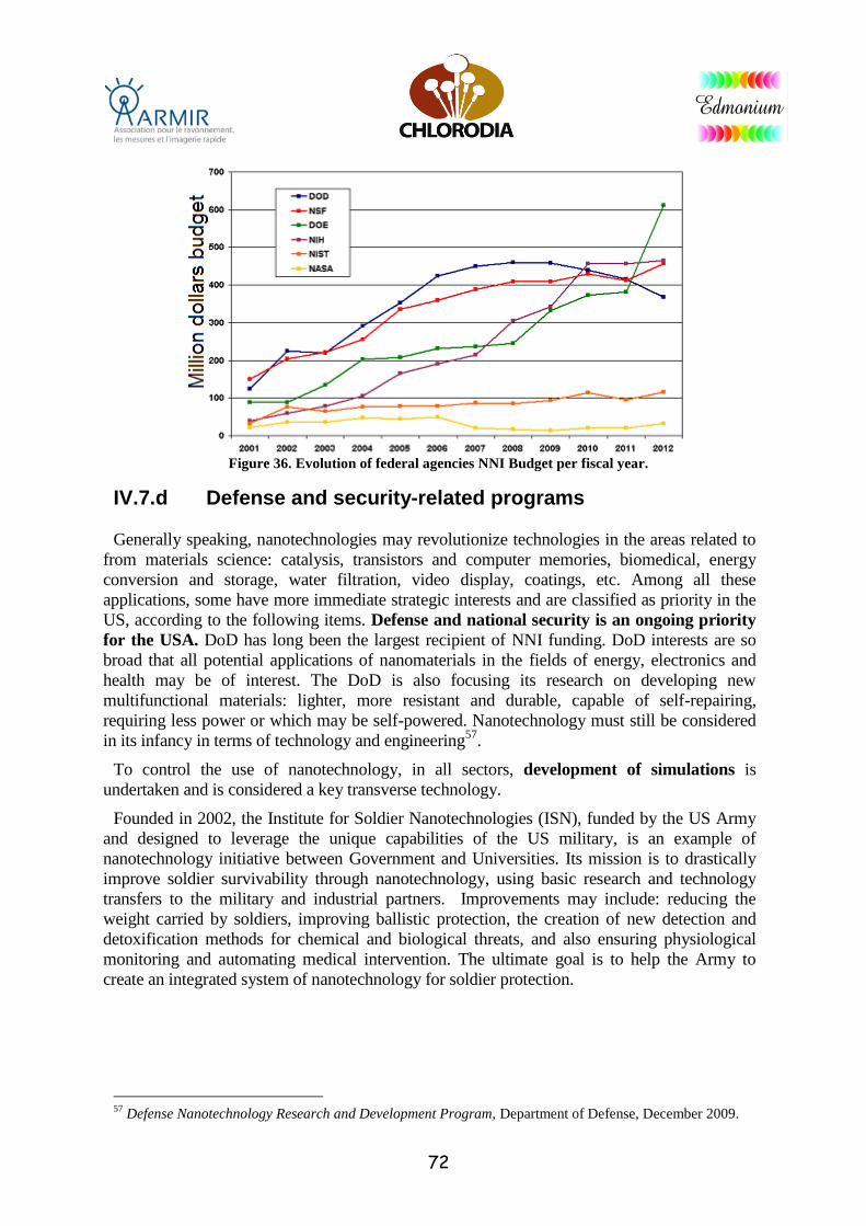
72
Figure 36. Evolution of federal agencies NNI Budget per fiscal year.
IV.7.d Defense and security-related programs
Generally speaking, nanotechnologies may revolutionize technologies in the areas related to
from materials science: catalysis, transistors and computer memories, biomedical, energy
conversion and storage, water filtration, video display, coatings, etc. Among all these
applications, some have more immediate strategic interests and are classified as priority in the
US, according to the following items. Defense and national security is an ongoing priority
for the USA. DoD has long been the largest recipient of NNI funding. DoD interests are so
broad that all potential applications of nanomaterials in the fields of energy, electronics and
health may be of interest. The DoD is also focusing its research on developing new
multifunctional materials: lighter, more resistant and durable, capable of self-repairing,
requiring less power or which may be self-powered. Nanotechnology must still be considered
in its infancy in terms of technology and engineering57
.
To control the use of nanotechnology, in all sectors, development of simulations is
undertaken and is considered a key transverse technology.
Founded in 2002, the Institute for Soldier Nanotechnologies (ISN), funded by the US Army
and designed to leverage the unique capabilities of the US military, is an example of
nanotechnology initiative between Government and Universities. Its mission is to drastically
improve soldier survivability through nanotechnology, using basic research and technology
transfers to the military and industrial partners. Improvements may include: reducing the
weight carried by soldiers, improving ballistic protection, the creation of new detection and
detoxification methods for chemical and biological threats, and also ensuring physiological
monitoring and automating medical intervention. The ultimate goal is to help the Army to
create an integrated system of nanotechnology for soldier protection.
57
Defense Nanotechnology Research and Development Program, Department of Defense, December 2009.

73
NNI 2011-2020 Strategic Plan All policies listed above are found in the NNI Strategic Plan published in February 2011
58,
and in the EHS strategy59
update. With respect to nanomaterials manufacture, solar energy
conversion and Nano electronics, the work plan has been defined in detail (Signature
Initiatives)60
. NNI is planning to launch five more such initiatives in the next five years.
Responsible development and societal issues will be emphasized, addressing the need for
exchange and communication, and encouraging vocations to ensure development of a skilled
workforce for the future. The flagship of the new strategy is control of nanomaterials and
products life cycle; this issue has been integrated in all research projects. The new strategy also
includes ethical, legal and social implications as essential components in the pursuit of
responsible development of the field, emphasizing the importance of communicating the
potential risks to all stakeholders (public, workers, etc.) to advance awareness of the
importance of these issues.
Six main areas have been identified:
“Nanomaterial Measurement Infrastructure”. Metrology, measuring instruments, instruments of detections or the protocols and references are essential tools which, for the moment, starved in the field of nanotechnology.
Characterization of human exposure to nanomaterials is the second field. The third field concerns human health.
The environment is the fourth field.
The fifth field includes risk evaluation and management methods.
A sixth field was added: IT, a new field compared to the 2008 strategy, a wide field transverse to all issues. Researchers and agencies need to be able to quickly share information and simulation models through creation of an infrastructure common to all agencies, control of data, protocol and reference quality as well as format of accumulated data. Computer simulation would then be, over the long term, the only way to correctly estimate the overall risks posed by a given nanomaterial. This would lead to more cooperation and collaboration between the different actors and disciplines, and ensure acceleration of the pace of progress. Faced with these challenges, an action and coordination strategy is more necessary than ever.
Support to technology transfer and commercialization of products is a priority, to transform
research promises. Otherwise, US voices clamoring for stopping costly research with few
results may become more numerous and popular. Getting to responsibly mass-produce
standardized nanomaterials, thus promises to be the challenge for 2020.
Since the launch of the nanotechnology program, it has always been clear in the USA that the
58
NNI strategic plan 2011, NSET, février 2011. – http://www.nano.gov/html/res/nnistrategicplan211.pdf 59
NNI 2011 EHS Strategy (Draft), NSET, 6 December 2010.
http://strategy.nano.gov/wp/wpcontent/uploads/2010/12/DraftEHSstrategy-17Dec2010-to-post.pdf 60
The first three Signature Initiatives – http://www.nano.gov/html/research/signature_initiatives.html
74
investment made through NNI is for the long term, for a minimum of 20 years61
. Based on
their experience and success, the United States are entering the program second decade,
confident of keeping their nanotechnology leadership for at least several years. DoD will
continue to coordinate its nanotechnology programs, which include DARPA and other federal
agencies. While nanotechnology basic research continues to mature, DoD anticipates that
expected results of applied research efforts will lead to development of advanced military
technologies. The DoD nanotechnology program remains robust and well balanced to enhance
Defense potential14
.
The DOJ National Institute of Justice (NIJ) has also two programs62
involving
nanotechnology. Development of DNA forensic research device is taking place in basic
research. Another project involves development of a quick, portable and low cost device to
warn of exposure to unexpected chemical and biological risks with sufficient response time to
ensure effective protection.
Legal issues
The use of nanomaterials in commercial products is growing faster than the understanding of
the risks these materials pose for human health and the environment. Gao (US Government
Accountability Office) has listed commercial nanotechnology applications63
and found EPA
(Environmental Protection Agency) information to be deficient. The EPA requires chemical
companies to periodically provide information on several currently available chemicals.
However, the EPA has not extended this requirement to nanomaterials, and is asked to address
this issue through the Clean Water Act to regulate this area.
61
MIHAIL C. ROCO, Nanotechnology Research Directions for Societal Needs in 2020, Spinger, October
2010. 62
National Nanotechnology Investment in the FY 2010 Budget, M. C. Roco, American Society of Mechanical
Engineers. 63
Nanomaterials Are Widely Used in Commerce, but EPA Faces Challenges in Regulating Risk, Government
Accountability Office, Committee on Environment and Public Works, U.S. Senate, mai 2010.
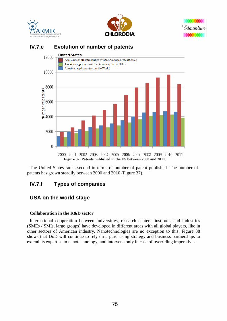
75
IV.7.e Evolution of number of patents
Figure 37. Patents published in the US between 2000 and 2011.
The United States ranks second in terms of number of patent published. The number of
patents has grown steadily between 2000 and 2010 (Figure 37).
IV.7.f Types of companies
USA on the world stage
Collaboration in the R&D sector
International cooperation between universities, research centers, institutes and industries
(SMEs / SMIs, large groups) have developed in different areas with all global players, like in
other sectors of American industry. Nanotechnologies are no exception to this. Figure 38
shows that DoD will continue to rely on a purchasing strategy and business partnerships to
extend its expertise in nanotechnology, and intervene only in case of overriding imperatives.
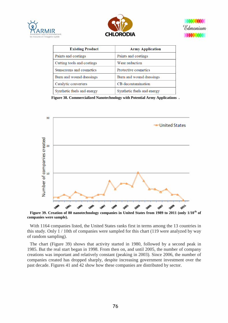
76
Figure 38. Commercialized Nanotechnology with Potential Army Applications
�.
Figure 39. Creation of 80 nanotechnology companies in United States from 1989 to 2011 (only 1/10
th of
companies were sample).
With 1164 companies listed, the United States ranks first in terms among the 13 countries in
this study. Only 1 / 10th of companies were sampled for this chart (119 were analyzed by way
of random sampling).
The chart (Figure 39) shows that activity started in 1980, followed by a second peak in
1985. But the real start began in 1998. From then on, and until 2005, the number of company
creations was important and relatively constant (peaking in 2003). Since 2006, the number of
companies created has dropped sharply, despite increasing government investment over the
past decade. Figures 41 and 42 show how these companies are distributed by sector.
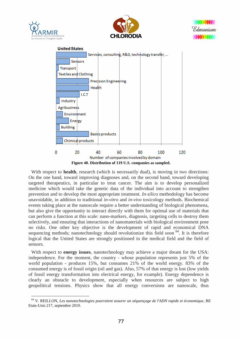
77
Figure 40. Distribution of 119 U.S. companies as sampled.
With respect to health, research (which is necessarily dual), is moving in two directions:
On the one hand, toward improving diagnoses and, on the second hand, toward developing
targeted therapeutics, in particular to treat cancer. The aim is to develop personalized
medicine which would take the genetic data of the individual into account to strengthen
prevention and to develop the most appropriate treatment. In-silico methodology has become
unavoidable, in addition to traditional in-vitro and in-vivo toxicology methods. Biochemical
events taking place at the nanoscale require a better understanding of biological phenomena,
but also give the opportunity to interact directly with them for optimal use of materials that
can perform a function at this scale: nano-markers, diagnosis, targeting cells to destroy them
selectively, and ensuring that interactions of nanomaterials with biological environment pose
no risks. One other key objective is the development of rapid and economical DNA
sequencing methods; nanotechnology should revolutionize this field soon 64
. It is therefore
logical that the United States are strongly positioned in the medical field and the field of
sensors.
With respect to energy issues, nanotechnology may achieve a major dream for the USA:
independence. For the moment, the country - whose population represents just 5% of the
world population - produces 15%, but consumes 21% of the world energy. 83% of the
consumed energy is of fossil origin (oil and gas). Also, 57% of that energy is lost (low yields
of fossil energy transformation into electrical energy, for example). Energy dependence is
clearly an obstacle to development, especially when resources are subject to high
geopolitical tensions. Physics show that all energy conversions are nanoscale, thus
64
V. REILLON, Les nanotechnologies pourraient assurer un séquençage de l'ADN rapide et économique, BE
Etats-Unis 217, septembre 2010.
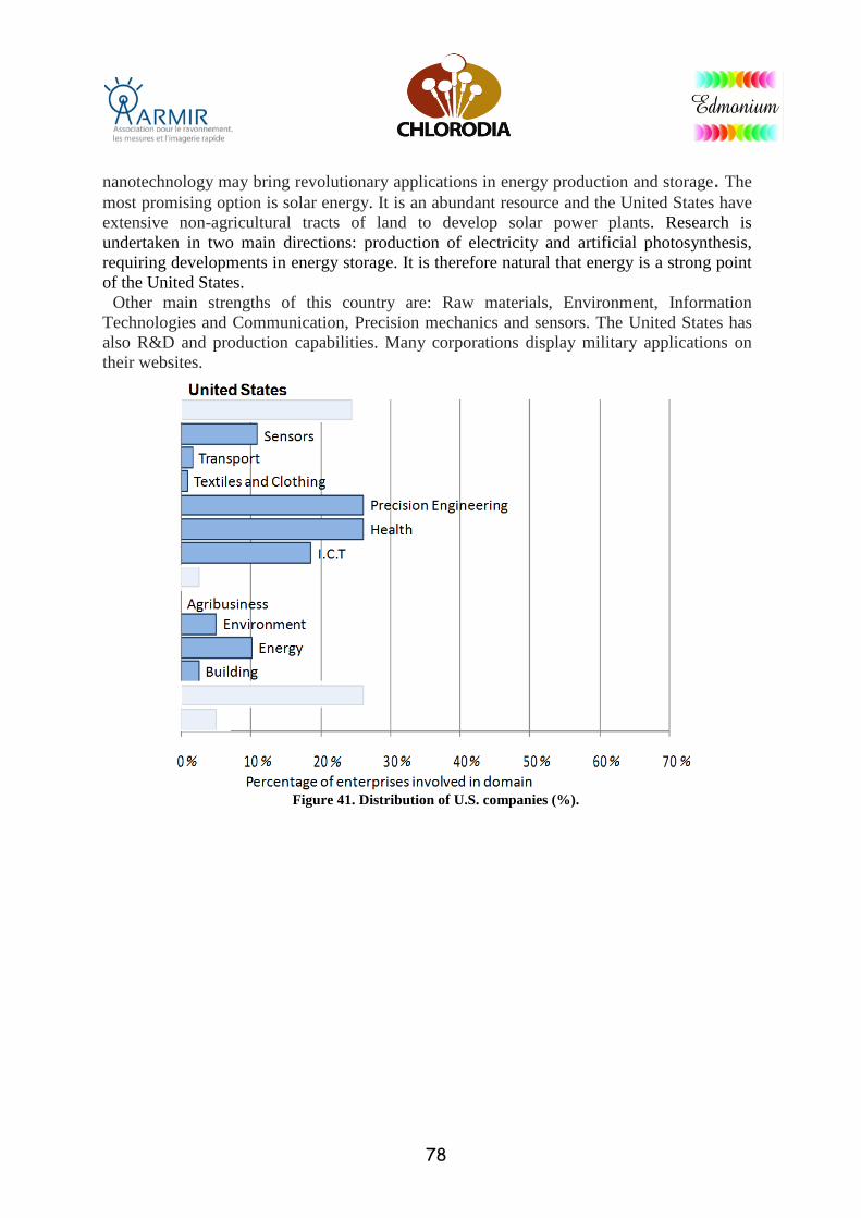
78
nanotechnology may bring revolutionary applications in energy production and storage. The
most promising option is solar energy. It is an abundant resource and the United States have
extensive non-agricultural tracts of land to develop solar power plants. Research is
undertaken in two main directions: production of electricity and artificial photosynthesis,
requiring developments in energy storage. It is therefore natural that energy is a strong point
of the United States.
Other main strengths of this country are: Raw materials, Environment, Information
Technologies and Communication, Precision mechanics and sensors. The United States has
also R&D and production capabilities. Many corporations display military applications on
their websites.
Figure 41. Distribution of U.S. companies (%).
79
Conclusion
Through the National Nanotechnology Initiative, the largest US program since the space
program, the United States are leaders in the field of nanotechnology. Major issues under
development are Nano electronics, the environment, energy conversion and storage,
development of nano-systems, and medicine, of which a main objective is development of
rapid and economical DNA sequencing methods, a field that nanotechnology should
revolutionize soon65
. There is also a very substantial investment in terms of simulation,
considered to be transverse technology, which should eventually enable the risks associated
with the use of nanotechnology to be assessed.
That country also strives, through metrology in particular, to define a set of standards and
protocols designed for data exchange between researchers, but also to protect individuals and
the environment.
The United States is the country that has funded most heavily the development of
nanotechnology, which also benefits from substantial private funding. A large number of
patents is filed in the USA, which have been able to build the world's largest industrial base.
Another advantage of the country is the a large number of venture capitalists (see Appendix 4,
Appendix 3). Support to technology transfer and commercialization of products is a national
priority.
65
V. REILLON, Les nanotechnologies pourraient assurer un séquençage de l'ADN rapide et économique, BE
Etats-Unis 217, septembre 2010.
80
IV.8 India
IV.8.a Master data
Population (2012) 1.2 billion
Area 3.3 million sq. km
Average Density 382 residents/sq. km
GDP (2011) $ 1,833 billion
GDP/capital (2012) $ 1,530
HDI (2012) 0.55
IV.8.b India’s efforts
There is in India a strong government will to develop nanotechnology and establish research
structures in the field.
In the late 90s, aware of nanotechnology importance for the future and of the country assets
(skilled workforce and low cost), the Indian government created three agencies with a mission
ensure promoting and developing nanotechnology R & D:
Department of Scientific and Industrial Research
Department of Biotechnology
Department of Science and Technology (DST); this agency plays a predominant role.
En 2001, a Nanoscience and Technology Initiative was entrusted to DST, chaired by Pr.
C.N.R. Rao, with making India a major player in the field as the target. It received a USD 15
million budget for years..
DSR has implemented a hundred research projects, distributed among the country research
institutes; there are ten nanoscience teams, in six centers dedicated to nanotechnology and one
dedicated to high power computing.
The concept of “Nanotechnology Cluster” appeared, designed to combine through
collaborations developed between institutes the skills necessary for projects on topics such as
development and control of thin films, Nano sensors, nanobiotechnology, superconductivity,
and “micro” and “nano” manufacturing processes.
In 2007, the Indian Government again showed its political will to make progress in the field
of nanotechnology, and started a new government initiative supported by $ 250 million
funding. Establishment of a tripartite governance comprising representatives of the State
(DST), of scientists and industry representatives was designed to develop strategic
partnerships between industry and research institutions.
Twenty large institutions are currently involved in R&D programs, which include the Indian
Institute of Science, the Jawaharial Nehru Center for Advanced Scientific Research,
universities like Anna University, the University of Delhi, defense agencies such as the
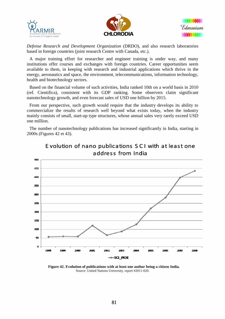
81
Defense Research and Development Organization (DRDO), and also research laboratories
based in foreign countries (joint research Centre with Canada, etc.).
A major training effort for researcher and engineer training is under way, and many
institutions offer courses and exchanges with foreign countries. Career opportunities seem
available to them, in keeping with research and industrial applications which thrive in the
energy, aeronautics and space, the environment, telecommunications, information technology,
health and biotechnology sectors.
Based on the financial volume of such activities, India ranked 10th on a world basis in 2010
(ref. Cientifica), consistent with its GDP ranking. Some observers claim significant
nanotechnology growth, and even forecast sales of USD one billion by 2015.
From our perspective, such growth would require that the industry develops its ability to
commercialize the results of research well beyond what exists today, when the industry
mainly consists of small, start-up type structures, whose annual sales very rarely exceed USD
one million.
The number of nanotechnology publications has increased significantly in India, starting in
2000s (Figures 42 et 43).
Figure 42. Evolution of publications with at least one author being a citizen India.
Source: United Nations University, report #2011-020.
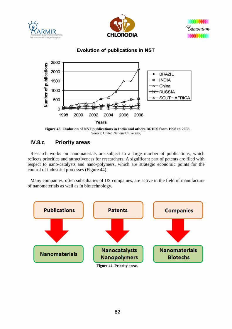
82
Figure 43. Evolution of NST publications in India and others BRICS from 1998 to 2008.
Source: United Nations University,
IV.8.c Priority areas
Research works on nanomaterials are subject to a large number of publications, which
reflects priorities and attractiveness for researchers. A significant part of patents are filed with
respect to nano-catalysts and nano-polymers, which are strategic economic points for the
control of industrial processes (Figure 44).
Many companies, often subsidiaries of US companies, are active in the field of manufacture
of nanomaterials as well as in biotechnology.
Figure 44. Priority areas.
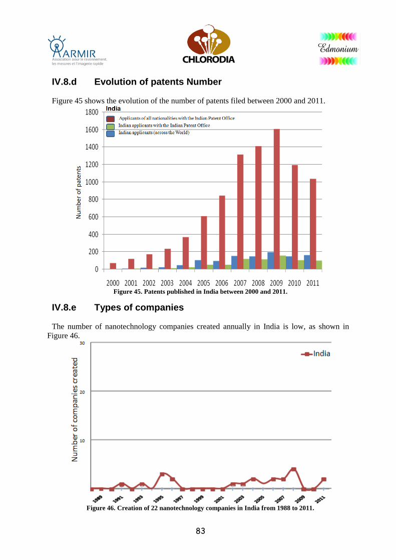
83
IV.8.d Evolution of patents Number
Figure 45 shows the evolution of the number of patents filed between 2000 and 2011.
Figure 45. Patents published in India between 2000 and 2011.
IV.8.e Types of companies
The number of nanotechnology companies created annually in India is low, as shown in
Figure 46.
Figure 46. Creation of 22 nanotechnology companies in India from 1988 to 2011.
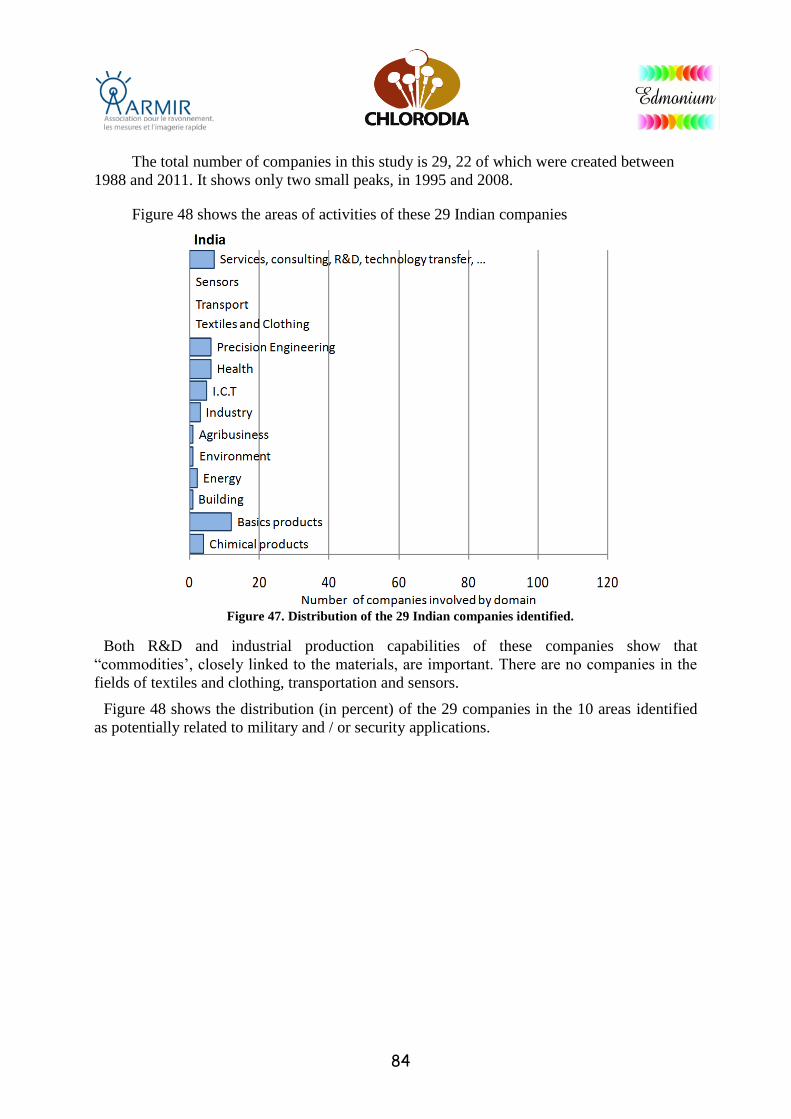
84
The total number of companies in this study is 29, 22 of which were created between
1988 and 2011. It shows only two small peaks, in 1995 and 2008.
Figure 48 shows the areas of activities of these 29 Indian companies
Figure 47. Distribution of the 29 Indian companies identified.
Both R&D and industrial production capabilities of these companies show that
“commodities’, closely linked to the materials, are important. There are no companies in the
fields of textiles and clothing, transportation and sensors.
Figure 48 shows the distribution (in percent) of the 29 companies in the 10 areas identified
as potentially related to military and / or security applications.
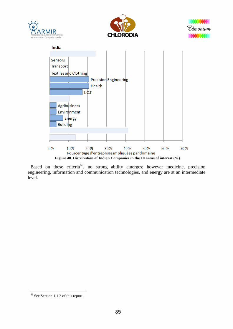
85
Figure 48. Distribution of Indian Companies in the 10 areas of interest (%).
Based on these criteria66
, no strong ability emerges; however medicine, precision
engineering, information and communication technologies, and energy are at an intermediate
level.
66
See Section 1.1.3 of this report.
86
Conclusion
Recognizing importance of nanotechnology for the future, India set up, in the late 1990s,
three agencies whose mission was to promote and develop nanotechnology R&D. Fields
chosen are: development and control of thin films, nano-sensors, nano-biotechnology,
superconductivity, as well as micro and nano fabrication processes, including nano-catalysts
and nano-polymers.
A major training effort for researcher and engineer training is under way, and many
institutions offer courses and exchanges with foreign countries, in particular with Canada.
Career opportunities seem available to them, in keeping with research and industrial
applications which thrive in the energy, aeronautics and space, the environment,
telecommunications, information technology, health and biotechnology sectors. As a result,
this number of publications has increased significantly.
While the industrial structure of India currently consists mainly of small, start-up type,
companies whose annual turnover rarely exceeds USD one million, the rapid development of
India could lead this country to quickly catch up in the field of nanotechnology.
87
IV.9 Indonesia
IV.9.a Master data
Population (2011) 245 millions
Area 1.9 million sq. km
Average population density 130 residents/sq. km
GDP (2011) $ 700 billion
GDP/inhabitant $ 2,900
HDI (2011) 0.62
IV.8.b Indonesia’s efforts
Nanoscience’s and nanotechnologies (NST) Programs in the Republic of Indonesia�
Indonesia, the 4th most populous country in the world and the country with the largest
predominantly Muslim population, is a democratic republic whose standard of living is very
low (GDP/capita ranked 150th in the world), despite an active investment policy, and an
economic growth which has not reached levels comparable to that of neighboring countries
(China and India).
This developing country status explains why Indonesia has remained behind in terms of
advanced technologies.
Interest in NST is relatively recent: in 2005, the government recognized how important NST
are in terms of research, and decided to invest.
A USD 27 million fund was created, to finance some sixty research projects based in
universities and research centers. The Indonesian Society for Nanotechnology (INM) manages
these projects and grants scholarships for young people to study NST.
Fields of interest are primarily food (need to improve food supply), energy (search for
alternative energy because of limited natural resources), health care (in particular treatment of
tropical diseases), the environment (monitoring of land, sea and airspace) and transportation
(whose importance stems from the vast expanse of the archipelago).
A few manufacturers, including Mochtar Riady Center for Nanotechnology and Bio-
engineering (MRCNB) are also involved in financing research projects, but we have no recent
information on the current status of these, nor on any industrial spinoffs.
Indonesia on the worldwide stage
An international symposium was held in 2011 in Bali: The 4th
Nanoscience and
Nanotechnology Symposium.
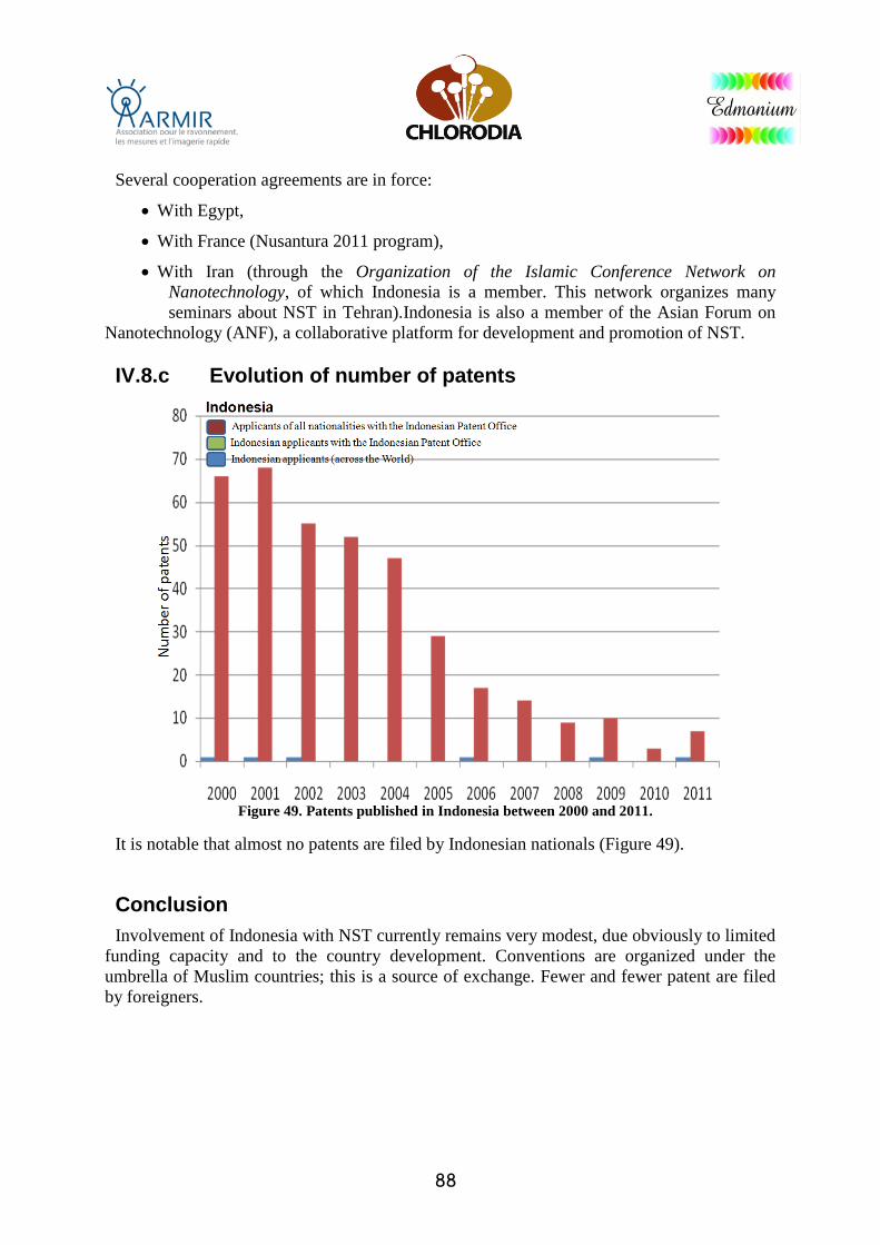
88
Several cooperation agreements are in force:
With Egypt,
With France (Nusantura 2011 program),
With Iran (through the Organization of the Islamic Conference Network on
Nanotechnology, of which Indonesia is a member. This network organizes many
seminars about NST in Tehran).Indonesia is also a member of the Asian Forum on
Nanotechnology (ANF), a collaborative platform for development and promotion of NST.
IV.8.c Evolution of number of patents
Figure 49. Patents published in Indonesia between 2000 and 2011.
It is notable that almost no patents are filed by Indonesian nationals (Figure 49).
Conclusion
Involvement of Indonesia with NST currently remains very modest, due obviously to limited
funding capacity and to the country development. Conventions are organized under the
umbrella of Muslim countries; this is a source of exchange. Fewer and fewer patent are filed
by foreigners.

89
IV.10 Israel
IV.10.a Master data
Population (2011) 7 millions
Area 20,000 sq. km
Average population density 367 residents/sq. km
GDP (2011) $ 217 billion
GDP/inhabitant (2010) $ 28,685
HDI (2010) 0.888
IV.10.b Measures and actions
Nanoscience and nanotechnology (NST) programs
Nanotechnologies have been defined as strategic for Israel, and they receive financial
support from US institutions Israeli defense-oriented SMEs and major companies are not shy
about their defense applications, in particular those including nanotechnology.
The dynamism of Israeli NST laboratories can be measured by number of publications and
patents, and by commercial success of Israeli companies. To enhance the efforts of
researchers and to maintain a reputation recognized worldwide, Israel has policies and
financial means: At first, the Nanotechnology National Committee67
was created to assess
this sector, and several five-year development and funding programs (2007-2011, 2012-2016)
were implemented, to male nanotechnology one of the spearheads of Israeli science. In fact, a
first nanotechnology program took place from 2003 to 2007, but it has been barely described
or mentioned. Over the past 10 years, more than USD 250 million have been invested in
infrastructure and research equipment.
The business model implemented is built on a “Funding triangle donation matching
program” model: universities, private donations, government, each contributing one third of
the financing (similar to the German business model). This is an excellent example of the use
of public funds, and it provides a very good return on investment.
Analysis of the Israeli government shows that all departments collaborate strongly in the
matter. Officially, several Israeli government-controlled centralizing agencies, and the
Nanotechnology Committee, have been established:
- INNI (Israel National Nanotechnology Initiative), created in 2001 to set up collaborations
67
Nanotechnology National Committee, appointed in 2000 by the Israeli TELEM coordination group,
composed by: Binyamin Netanahu Prime Minister, Minister of Economic Strategy, Minister of Health, Mr
Yaalon Deputy Prime Minister and Minister of Strategic Affairs, Deputy Prime Minister, Minister of Regional
Development of the Negev and Galilee, 1st Deputy Minister and Minister of Defence, D. Meridor 1st Deputy
Minister and Minister of intelligence and atomic Energy, the Minister of Science and Technology, the Minister
of Industry, Trade and Employment, the Minister for national Infrastructure, the Minister of Civil Defence,
Minister for the Environment, the Vice-Minister of Finance, Deputy Minister of Health.

90
between industry, science and academia, and ambitious long-term research and development
programs, as well as investment and infrastructure to be among best in the world.
- MATIMOP, created in 2006, is the operational framework agency of the OCS (Office of
the Chief Scientist) of the Ministry of Industry, Trade and Labour (MOITAL). Matimop is the
Israeli agency for R&D/industry cooperation, responsible for strong promotion and support
policies to build Israel’s industrial infrastructure, and to strengthen industrial innovation and
entrepreneurship. This agency initiates and develops international R & D cooperation
between Israel and foreign companies.
Key actors:
Academic Institutions: Israel hosts six research institutes/universities which are among
the best in the world; each of them has its own advanced programs in nanoscience,
focused on a specific discipline and research and its own internal methods: Bar Ilan
University (Bar Ilan Center for Advanced Materials and Nanotechnology, mostly
defense applications), Technion Israel Institute (Russell Berrie Nanotechnology
Institute-RBNI), Tel Aviv University Research Institute for Nanoscience and
Nanotechnology, Ben Gurion University of the Negev, Weizmann Institute of Science,
Hebrew University of Jerusalem.Nanotechnology start-ups: In 2007, Israel had the
third largest concentration of start-ups in the world.Companies: Israel has identified
the crucial role of industry to move nanotechnology to common and widespread use,
e.g. Elbit, Plasan Sasa-Raphael, Plassan, Israel Aircraft Industries, etc.Venture
Capital Investors: Israel is ranked among the coutries which most use foreign venture
capital and business angels.
Comments:
Key technology companies maintain active R&D centers in Israel. Global economic
surveys rank Israel among the most attractive nations for developing advanced
technologies.
• The Israeli labor market is among the most skilled in the world: 20% of the workforce
has a university degree. For 10,000 employees, 140 have a science or technology
degree, and 135 an engineering degree. Similar ratios are much lower in the USA,
Japan and Europe.
In 2007, Israel established the nanoscience sector as a priority national project, to create the
research infrastructure with six universities which supports companies in this field. The
thematic distribution of 618 Israeli scholars in the field of nanotechnology is as follows:
Environment and Energy: 22
Nanotechnology general sciences: 15
Materials and Interfaces: 158
Nanotechnology & Nanomedicine: 153
Nanochemistry: 41
Nanomaterials and Nanoparticles: 91
Optics and Photonics: 96
Other: 42
In addition to these academic researchers, there are 320 junior scientists / postdocs, 816
doctoral students and 915 master's student (September 2011 Figures). This translates into
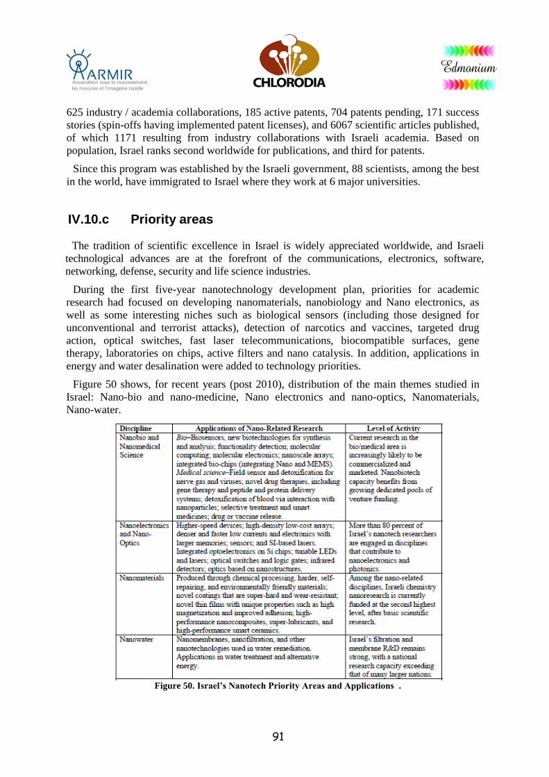
91
625 industry / academia collaborations, 185 active patents, 704 patents pending, 171 success
stories (spin-offs having implemented patent licenses), and 6067 scientific articles published,
of which 1171 resulting from industry collaborations with Israeli academia. Based on
population, Israel ranks second worldwide for publications, and third for patents.
Since this program was established by the Israeli government, 88 scientists, among the best
in the world, have immigrated to Israel where they work at 6 major universities.
IV.10.c Priority areas
The tradition of scientific excellence in Israel is widely appreciated worldwide, and Israeli
technological advances are at the forefront of the communications, electronics, software,
networking, defense, security and life science industries.
During the first five-year nanotechnology development plan, priorities for academic
research had focused on developing nanomaterials, nanobiology and Nano electronics, as
well as some interesting niches such as biological sensors (including those designed for
unconventional and terrorist attacks), detection of narcotics and vaccines, targeted drug
action, optical switches, fast laser telecommunications, biocompatible surfaces, gene
therapy, laboratories on chips, active filters and nano catalysis. In addition, applications in
energy and water desalination were added to technology priorities.
Figure 50 shows, for recent years (post 2010), distribution of the main themes studied in
Israel: Nano-bio and nano-medicine, Nano electronics and nano-optics, Nanomaterials,
Nano-water.
Figure 50. Israel’s Nanotech Priority Areas and Applications
�.
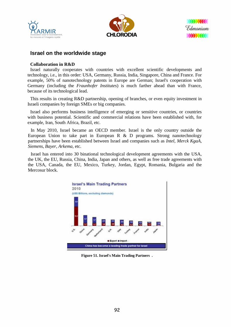
92
Israel on the worldwide stage
Collaboration in R&D
Israel naturally cooperates with countries with excellent scientific developments and
technology, i.e., in this order: USA, Germany, Russia, India, Singapore, China and France. For
example, 50% of nanotechnology patents in Europe are German; Israel's cooperation with
Germany (including the Fraunhofer Institutes) is much farther ahead than with France,
because of its technological lead.
This results in creating R&D partnership, opening of branches, or even equity investment in
Israeli companies by foreign SMEs or big companies.
Israel also performs business intelligence of emerging or sensitive countries, or countries
with business potential. Scientific and commercial relations have been established with, for
example, Iran, South Africa, Brazil, etc.
In May 2010, Israel became an OECD member. Israel is the only country outside the
European Union to take part in European R & D programs. Strong nanotechnology
partnerships have been established between Israel and companies such as Intel, Merck KgaA,
Siemens, Bayer, Arkema, etc.
Israel has entered into 30 binational technological development agreements with the USA,
the UK, the EU, Russia, China, India, Japan and others, as well as free trade agreements with
the USA, Canada, the EU, Mexico, Turkey, Jordan, Egypt, Romania, Bulgaria and the
Mercosur block.
Figure 51. Israel's Main Trading Partners�
.

93
IV.10.d Evolution of number of patents
Figure 52. Patents published in Israel between 2000 and 2011.
In terms of number of patents, Israel ranks 11th among the 13 countries in this study. The
difference in the number of patents filed by Israeli and other nationalities is significant
(Figure 52). While the overall number of patents filed between 2000 and 2010 increased,
patents filed by Israelis increased only very slightly.
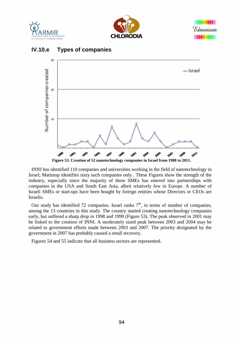
94
IV.10.e Types of companies
Figure 53. Creation of 52 nanotechnology companies in Israel from 1988 to 2011.
INNI has identified 110 companies and universities working in the field of nanotechnology in
Israel; Matimop identifies sixty such companies only . These Figures show the strength of the
industry, especially since the majority of these SMEs has entered into partnerships with
companies in the USA and South East Asia, albeit relatively few in Europe. A number of
Israeli SMEs or start-ups have been bought by foreign entities whose Directors or CEOs are
Israelis.
Our study has identified 72 companies. Israel ranks 7th
, in terms of number of companies,
among the 13 countries in this study. The country started creating nanotechnology companies
early, but suffered a sharp drop in 1998 and 1999 (Figure 53). The peak observed in 2001 may
be linked to the creation of INNI. A moderately sized peak between 2003 and 2004 may be
related to government efforts made between 2003 and 2007. The priority designated by the
government in 2007 has probably caused a small recovery.
Figures 54 and 55 indicate that all business sectors are represented.
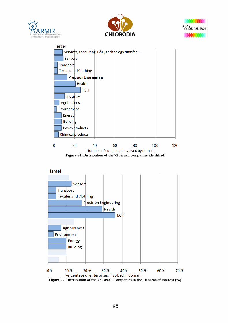
95
Figure 54. Distribution of the 72 Israeli companies identified.
Figure 55. Distribution of the 72 Israeli Companies in the 10 areas of interest (%).
96
Based on these criteria68
, Israel has strong capabilities in information and communication
technologies and medical applications and average capabilities in precision mechanics,
sensors, energy, construction and food processing.
Conclusion
In terms of nanotechnology, Israel appears as a benchmark country, together with
Germany and the United States.
In Israel, nanotechnologies have been defined as strategic by the state; they receive financial
support from American institutions. They are at least about 85% dual. This analysis shows that
there are many Israeli companies in the information and communication technologies and the
medical. fields
68
See Section 7.1.3 of this report.
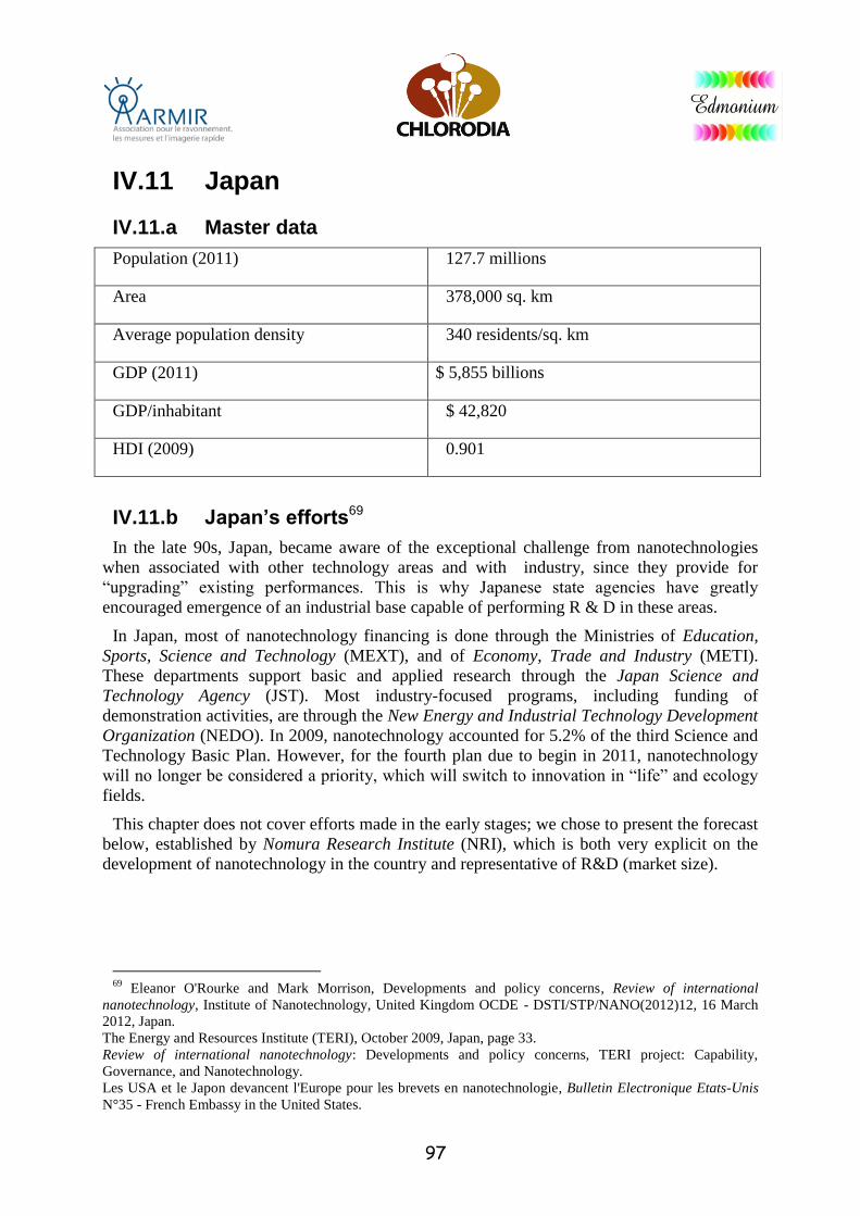
97
IV.11 Japan
IV.11.a Master data
Population (2011) 127.7 millions
Area 378,000 sq. km
Average population density 340 residents/sq. km
GDP (2011) $ 5,855 billions
GDP/inhabitant $ 42,820
HDI (2009) 0.901
IV.11.b Japan’s efforts69
In the late 90s, Japan, became aware of the exceptional challenge from nanotechnologies
when associated with other technology areas and with industry, since they provide for
“upgrading” existing performances. This is why Japanese state agencies have greatly
encouraged emergence of an industrial base capable of performing R & D in these areas.
In Japan, most of nanotechnology financing is done through the Ministries of Education,
Sports, Science and Technology (MEXT), and of Economy, Trade and Industry (METI).
These departments support basic and applied research through the Japan Science and
Technology Agency (JST). Most industry-focused programs, including funding of
demonstration activities, are through the New Energy and Industrial Technology Development
Organization (NEDO). In 2009, nanotechnology accounted for 5.2% of the third Science and
Technology Basic Plan. However, for the fourth plan due to begin in 2011, nanotechnology
will no longer be considered a priority, which will switch to innovation in “life” and ecology
fields.
This chapter does not cover efforts made in the early stages; we chose to present the forecast
below, established by Nomura Research Institute (NRI), which is both very explicit on the
development of nanotechnology in the country and representative of R&D (market size).
69
Eleanor O'Rourke and Mark Morrison, Developments and policy concerns, Review of international
nanotechnology, Institute of Nanotechnology, United Kingdom OCDE - DSTI/STP/NANO(2012)12, 16 March
2012, Japan.
The Energy and Resources Institute (TERI), October 2009, Japan, page 33.
Review of international nanotechnology: Developments and policy concerns, TERI project: Capability,
Governance, and Nanotechnology.
Les USA et le Japon devancent l'Europe pour les brevets en nanotechnologie, Bulletin Electronique Etats-Unis
N°35 - French Embassy in the United States.

98
Forecasting the size of the Japanese nanotechnology products market
2010/2015
Nomura Research Institute, Ltd - July 20, 2006
Nomura Research Institute Ltd has forecast the size of the market for nanotechnology-
related products on a domestic production basis (Figure 56). This projection covers eight
basic elements of this market. These items are automotive consumer products, bicycles
components, products for industrial robots, dental, orthopedic and medical products, energy-
or environment-related electronic products, materials, and measuring devices. Projections
showed that the market was Yen 942.1 billion as a whole in 2004, and is expected to grow to
Yen 5649.8 billion in 2010 and Yen 23,061.2 billion by 2015.
NRI believes that said market growth will result from: (1) existing market growth by means
of nanotechnology, (2) replacement of existing products with products using nanotechnology
and (3) emergence of a new market through practical application of nanotechnologies.
Therefore, methods that can be commonly used for these topics were adopted for market size
calculation. More specifically, NRI has assumed nanotechnology products growth rates of
replacing existing products with products using nanotechnology and has estimated the cost
ratio of the nanotechnology part in each product. The market size was then calculated by
multiplying the actual production amount (value of shipments) for existing products by these
rates.
NRI believes that, for new companies to be created, it is essential that knowledge be shared
by all those engaged in related fields, such as research, product development, manufacturing
and marketing. One way to achieve this goal of shared knowledge is
“technology visualization.”
The table below contains estimates of various types of consumer products, allowing the
reader to identify the strengths of Japanese nanotechnology industry and assess possible
partnership opportunities. These results compare to the type of Japanese industries in 2010,
which in turn corresponds to the existing (number of enterprises by theme) in these areas.
This distribution is presented in detail further down. Peaks are consistent with those forecast
for 2010 by NRI, which give credibility to forecasts for 2015.
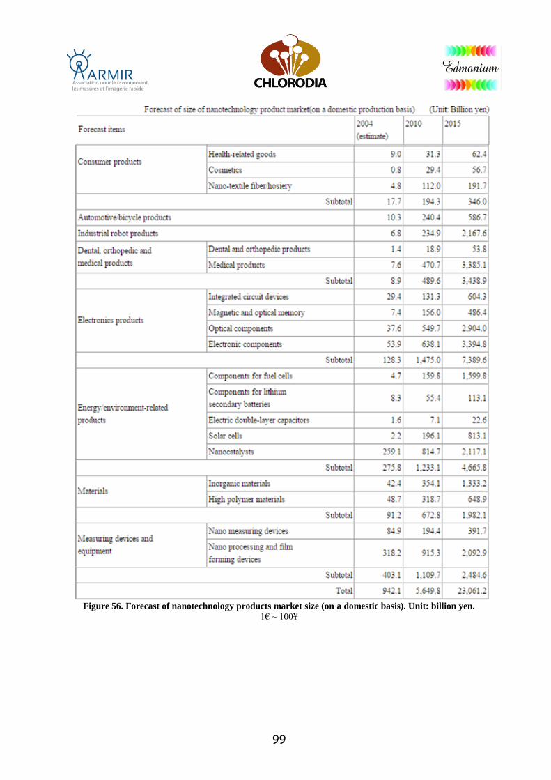
99
Figure 56. Forecast of nanotechnology products market size (on a domestic basis). Unit: billion yen.
1€ ~ 100¥
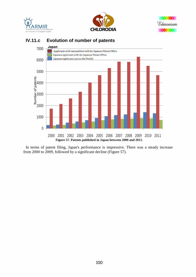
100
IV.11.c Evolution of number of patents
Figure 57. Patents published in Japan between 2000 and 2011.
In terms of patent filing, Japan's performance is impressive. There was a steady increase
from 2000 to 2009, followed by a significant decline (Figure 57).
101
IV.11.d Types of companies
Figure 58. Creation of 43 nanotechnology companies in Japan from 1988 to 2011.
The total number of companies listed in this study is 112, including 43 created between
1988 and 2011 (rank: 4th out of the 13 countries in this study). Nanotechnology activities are
thus performed largely by existing firms, and type field has not generated many business start-
ups. The chart shows initial start of activity in 1995. There is a double peak, in 2000 and
2002, maybe related to the double peak of patents visible 7 years later. Then, after 2004,
business creation virtually stopped.
Figure 58 shows the activity areas of these companies.
102
Figure 59. Distribution of 112 identified Japanese companies (%).
The best represented areas are precision engineering and information and communication
technologies, followed by commodities.
Figure 60 shows the distribution (in percent) of the 112 companies in the 10 areas identified
as potentially related to military and / or security applications..
103
Figure 60. Distribution (%) of 112 Japanese companies in the 10 selected areas.
Conclusion
Japan has a strong industrial base dedicated to nanotechnology.
Forecasts, until 2015, made by Nomura Research Institute, about the size of the Japanese
market for nanotechnology products, are essentially consistent with the analysis of the studied
company types, which highlights those areas currently showing strong industrial applications.
104
IV.12 United Kingdom
IV.12.a Master data
Population (2011) 62 millions
Area 0,2 million sq. km
Average population density 260 residents/sq. km
GDP (2011) USD 2,480 billion
GDP/inhabitant (2010) USD 35,000
HDI (2010) 0.884
IV.12.b UK’s efforts
In the UK, public nanotechnology research is coordinated by the Nanotechnology Research
Coordination Group (NRCG), chaired by Defra 70
; it includes ministries and government
agencies, research councils and related administrations.
(see Appendix 5: United Kingdom, Appendix 1)
Within the UK Research Councils, RCUK Nanotechnology Group, led by EPSRC71
,
coordinating a program between all research councils, some of which may have their own
nanotechnology programs:
Nanoscience through engineering to application (EPSRC);
Environmental Nanoscience Initiative, involving the Natural Environment Research
Council, Defra and the Environment Agency.
Within this structure, responsibility for basic research is assigned to research councils.
There are about 20 EPSRC-funded universities working in the field of nanotechnology72
.
Currently, the UK does not have a government program underway to support
nanotechnology. There are a number of existing projects, but the current plans for science
funding by the Government for 2011-2015, as defined in the various research council
documents, reveals no future role for nanotechnology. The previous inter-councils program
“engineering through the application of nanoscience” has been abandoned.
All inter-Councils programs are inscribed in social issues such as population aging,
environmental change, global security, energy, food security and the digital economy. The
70
Department for Environment, Food and Rural Affairs. 71
Engineering and Physical Sciences Research Council 72
Oxford (bio-nanotechnologies), Cambridge (nanofabrication), Durham, Sheffield, Surrey, Birmingham,
Nottingham, Starthclyde, Southampton, Glasgow, Manchester, Bristol, Edinburgh, Cardiff, Leeds, Queen’s
University of Belfast, Bath, Exeter, University College of London et Imperial College of London.
105
Delivery Plan for Engineering and Physical Sciences of the Research Council, which is the
leading council for nanotechnologies, doesn't even mention the word73.
Defining precisely UK government spending in terms of R&D for nanotechnology is
difficult, mainly for lack of distinction between micro- and nanotechnology (MNT). That
being said, public spending on nanotechnology over the last 12 years can be estimated at over
£ 640 million.
Over the past five years, the government has invested significantly in the MNT community,
including for example £ 90 million aimed at developing a new network of equipment and
services.
EPSRC has invested £ 253 million since 2003, distributed on a portfolio of over 400
projects, the most important of them being:
Grand Challenge for Healthcare (19 projects totaling £ 16.6 million), and
Grand Challenge for Energy (2 projects totaling £ 6.78 million).
The Ministry of Defense, EPSC, the Biotechnology and Biological Sciences Research
Council (BBSRC) and the Medical Research Council (MRC) have contributed £ 19.4 million
(£ 3.4 million, £ 10 million, £ 3 million and £ 3 million, respectively) for the implementation
of multidisciplinary research centers in nanotechnology (Interdisciplinary Research Centres -
IRC).
Regarding legislation, the Department of Trade & Industry (DTI) published a report in
December 2006. This document identifies a number of regulatory gaps74
. However, it
concludes that they do not exist because of omission but rather due to lack of knowledge
about the effects of nanoparticles on human health and the environment.
On June 1, 2007, the European REACH regulation75
entered into force. Except for certain
types of nanomaterials (such as fullerene), which are considered as new and addressed
specifically by this regulation, particle size does not influence the way materials are classified.
This means that most nanomaterials are classified and treated as if they were massive
materials.
The British government has supported a number of initiatives to promote dialogue on
nanotechnologies. For example:
Nanodialogues which, under the Sciencewise program, covers various applications of
nanotechnology. This initiative was supported to the tune of £ 120,000 by the DTI,
equivalent funding being provided by other sources.Small Talk, with a budget of £
50,000 (around € 73,000), which implies discussion of nanotechnology with the
public and scientists.
73
It's the same for the last strategy paper from the Technology Strategy Board, body responsible for supporting
R & D for products close of the market, for which nanotechnologies are "now incorporated in all subjects where
there are such opportunities." 74
Defra identifies a number of regulatory gaps, particularly with regard to threshold values and exemptions
laid down in existing legislation, current scientific knowledge and understanding of risk, lack of information and
vagueness of certain definitions, and finally, reliable and validated methods to control exposure and possible
effects on human health and the environment. 75
Regulation on the Registration, Evaluation, Authorization and Restriction of Chemicals.
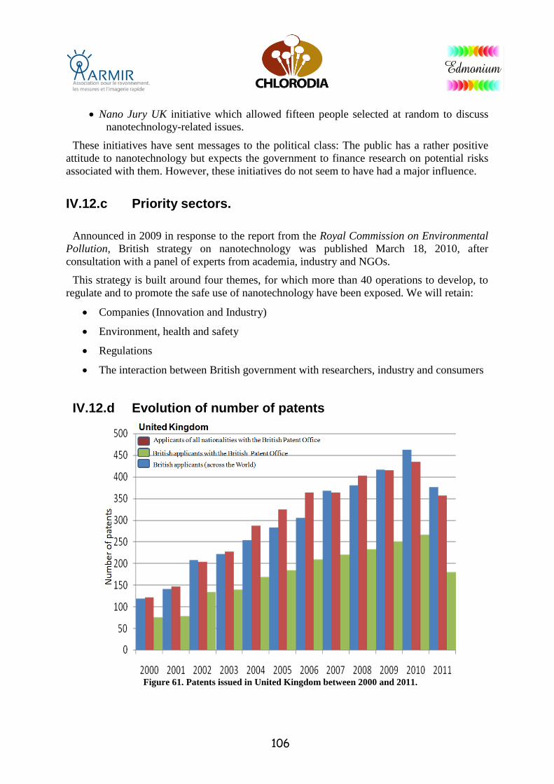
106
Nano Jury UK initiative which allowed fifteen people selected at random to discuss
nanotechnology-related issues.
These initiatives have sent messages to the political class: The public has a rather positive
attitude to nanotechnology but expects the government to finance research on potential risks
associated with them. However, these initiatives do not seem to have had a major influence.
IV.12.c Priority sectors.
Announced in 2009 in response to the report from the Royal Commission on Environmental
Pollution, British strategy on nanotechnology was published March 18, 2010, after
consultation with a panel of experts from academia, industry and NGOs.
This strategy is built around four themes, for which more than 40 operations to develop, to
regulate and to promote the safe use of nanotechnology have been exposed. We will retain:
Companies (Innovation and Industry)
Environment, health and safety
Regulations
The interaction between British government with researchers, industry and consumers
IV.12.d Evolution of number of patents
Figure 61. Patents issued in United Kingdom between 2000 and 2011.
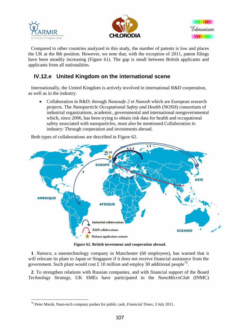
107
Compared to other countries analyzed in this study, the number of patents is low and places
the UK at the 8th position. However, we note that, with the exception of 2011, patent filings
have been steadily increasing (Figure 61). The gap is small between British applicants and
applicants from all nationalities.
IV.12.e United Kingdom on the international scene
Internationally, the United Kingdom is actively involved in international R&D cooperation,
as well as in the industry.
Collaboration in R&D: through Nanosafe 2 et Nanosh which are European research
projects. The Nanoparticle Occupational Safety and Health (NOSH) consortium of
industrial organizations, academic, governmental and international nongovernmental
which, since 2006, has been trying to obtain risk data for health and occupational
safety associated with nanoparticles, must also be mentioned.Collaboration in
industry: Through cooperation and investments abroad.
Both types of collaborations are described in Figure 62.
Figure 62. British investment and cooperation abroad.
1. Nanoco, a nanotechnology company in Manchester (60 employees), has warned that it
will relocate its plant to Japan or Singapore if it does not receive financial assistance from the
government. Such plant would cost £ 10 million and employ 30 additional people76
.
2. To strengthen relations with Russian companies, and with financial support of the Board
Technology Strategy, UK SMEs have participated in the NanoMicroClub (INMC)
76
Peter Marsh, Nano-tech company pushes for public cash, Financial Times, 3 July 2011.
108
international event in Russia. Some of these SMEs were already in a funding application
process with RUSNANO77
.
3. The existing relationship between the UK and South Korea have been strengthened by the
signing of a Memorandum of Understanding (MoU) between STFC and the Korea Research
Council on basic science and technology (KRCF)78
.
4. RUSNANO is investing $ 700 million in Plastic Logic (flexible plastic electronic display,
UK). This will fund a plastic electronics factory in Zelenograd79
.
5. RUSNANO plans $ 900 million for a pharmaceutical project with UK companies 80
.
6. British SMEs visited the Nanotech 2011 show in Tokyo 81
.
7. Ten 10 British industrialists took part in the Eilat-Eliot Israeli conference, funded by
Science and Innovation Network (NAS) to foster productive partnerships in the field of
renewable energy82
.
8. RUSNANO and Celtic Pharma Holdings (investment funds, Great Britain) are creating
the Russian international biopharmaceutical company Pro Bono Bio. The total amount of
money that might be invested by RUSNANO is $ 300 million83
.
9. Collaboration between Brazil and the United Kingdom as part of a network on innovation
in the biosciences. To enable a transfer of knowledge and to promote the interaction of
members of Biosciences KTN with part of the investment community from Brazil84
.
10. SBRI & MOD armor and protection contest85
.
11. The Centre for Defense Enterprise (CDE) of the Ministry of Defense has launched a
contest to find new low cost technologies for future complex weapons 86
.
British companies occasionally encounter difficulties to finance their development. In this
context, they turn to foreign countries such as Russia. Production lines are then relocated.
77
Fionna Brewer, Announces Success of UK Nanotechnology Mission to Russia, NanoKTN, 24 June 2011. 78
Lucy Stone, UK and Korea stand together for the future of science, STFC Rutherford Appleton Laboratory,
27 October 2010. 79
Rusnano Finalizes Investment in Plastic Logic: $700 Million Total Investment Project Will Include Building
World’s Largest Commercial Plastic Electronics Factory in Zelenograd, Rusnano, 18 January 2011. 80
RusNano plans $900 for a pharmaceutical project with British business, RIA Novosti, 25 November 2011. 81
Del Stark,UK Nanotechnology SMEs take to Japan for business, Institute of Nanotechnology,22 February
2011. 82
Arnold Black, ES KTN secures funding for Renewable Energy Mission to Israel, 7 September 2010 83
Rusnano and Celtic Pharma Holdings (Great Britain) Establish International Pharmaceutical Company Pro
Bono Bio, Rusnano, 12 september 2011. 84
The network will invest in venture capital in Brazil, with direct access to UK companies that are particularly
suited to the markets of the Brazilian biotechnology and to the member companies that might have an interest in
seeking financing and/or collaborations in Brazil. 85
Novel Technologies for Complex Weapons, Ministry of Defence; DSTL, 27 January 2011. 86
Toby Gill, Novel technologies for complex weapons, 6 January 2011.
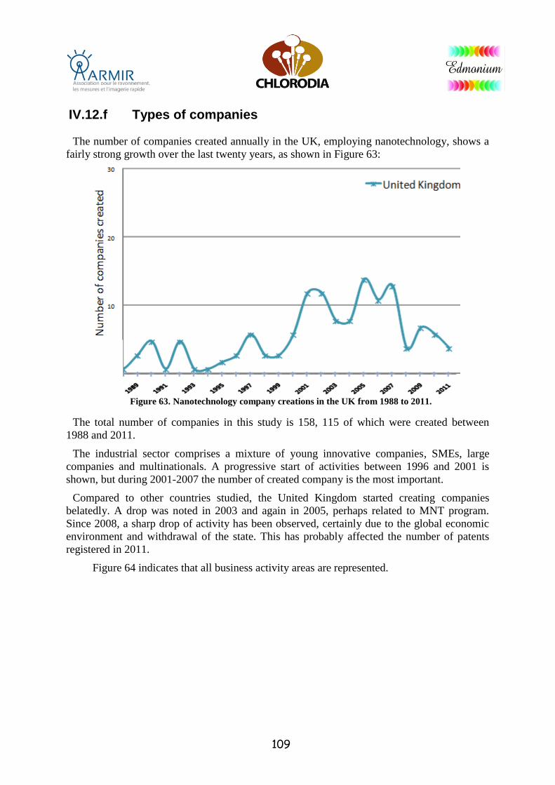
109
IV.12.f Types of companies
The number of companies created annually in the UK, employing nanotechnology, shows a
fairly strong growth over the last twenty years, as shown in Figure 63:
Figure 63. Nanotechnology company creations in the UK from 1988 to 2011.
The total number of companies in this study is 158, 115 of which were created between
1988 and 2011.
The industrial sector comprises a mixture of young innovative companies, SMEs, large
companies and multinationals. A progressive start of activities between 1996 and 2001 is
shown, but during 2001-2007 the number of created company is the most important.
Compared to other countries studied, the United Kingdom started creating companies
belatedly. A drop was noted in 2003 and again in 2005, perhaps related to MNT program.
Since 2008, a sharp drop of activity has been observed, certainly due to the global economic
environment and withdrawal of the state. This has probably affected the number of patents
registered in 2011.
Figure 64 indicates that all business activity areas are represented.

110
Figure 64. Distribution of the UK companies identified.
The strong presence in precision mechanics, specifically metrology, is related to the British
interest to the potential toxicity of nanomaterials87
. The UK is more focused on nanomaterial
integration than about their manufacture (commodities). Indeed, production of nanomaterials
isn't necessarily where the biggest financial margin is. Value can be generated by theoretical
development, design, manufacture of new techniques, sale of intellectual properties and
licensing to other countries. The UK has a good industrial capacity for thin layer deposition
(precision mechanics).
Figure 65 shows the distribution (in percent) of the 158 companies in the 10 areas identified
as potentially related to military and / or security applications.
87
Metrology is crucial for the detection, measurement and classification of nanomaterials. It can also measure
workplace exposure and create standards used in regulation or toxicological studies.
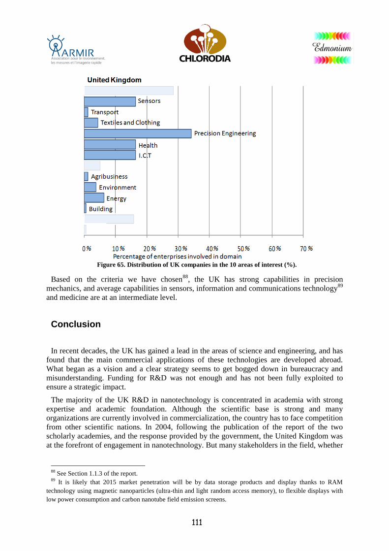
111
Figure 65. Distribution of UK companies in the 10 areas of interest (%).
Based on the criteria we have chosen88
, the UK has strong capabilities in precision
mechanics, and average capabilities in sensors, information and communications technology89
and medicine are at an intermediate level.
Conclusion
In recent decades, the UK has gained a lead in the areas of science and engineering, and has
found that the main commercial applications of these technologies are developed abroad.
What began as a vision and a clear strategy seems to get bogged down in bureaucracy and
misunderstanding. Funding for R&D was not enough and has not been fully exploited to
ensure a strategic impact.
The majority of the UK R&D in nanotechnology is concentrated in academia with strong
expertise and academic foundation. Although the scientific base is strong and many
organizations are currently involved in commercialization, the country has to face competition
from other scientific nations. In 2004, following the publication of the report of the two
scholarly academies, and the response provided by the government, the United Kingdom was
at the forefront of engagement in nanotechnology. But many stakeholders in the field, whether
88
See Section 1.1.3 of the report. 89
It is likely that 2015 market penetration will be by data storage products and display thanks to RAM
technology using magnetic nanoparticles (ultra-thin and light random access memory), to flexible displays with
low power consumption and carbon nanotube field emission screens.

112
from industry, academia, learned societies and NGOs share the view that the country has lost
the leading position. However, it could regain it if actions were resolutely implemented.
The UK is also plagued by many concerns:
What might be the impact of new nanomaterials on human health?
What types of applications might arise from the convergence of nanotechnology, on
one hand, and biotechnology, computer science or artificial intelligence, on the other?
Are the current regulatory frameworks relevant?
However the Council for Science and Technology believes that the government has
advanced significantly on a number of commitments (international cooperation,
standardization, application of the precautionary principle, collaboration with industry,
reporting system on a voluntary basis, etc.).
See Appendix 5, Appendix 2
113
IV.13 Russia
IV.13.a Master data
Population (2012) 143 millions
Area 17 million sq. km
Average population density 8,3 residents/sq. km
GDP (2011) 1,884 billion $
GDP/inhabitant 15,9000$
HDI (2009) 0.817
IV.13.b Russia’s efforts
After a difficult decade of declining funding and brain drain, conditions for development of
Russian R&D have become favorable again. In this context, development of nanotechnology
has become a priority in Russia; it is coordinated at the highest political level and enjoys
significant resources.
While some countries such as the US, Germany and Japan, have made nanotechnology a
priority of their research and innovation policy in years 1990, there was also intense activity
in the leading Russian scientific centers for the development of nanotechnologies during this
period. Russia has therefore not taken any significant delay in relation to Western advances.
Indeed, based on very good basic knowledge of solid physics, crystallography, quantum
mechanics, theoretical physics, laser physics, biophysics and genetics, Russian research has
been able to take the turn to these new technologies. However, until 2004-2005, organization
of nanotechnology R&D remained relatively uncoordinated, due to a lack of consultation of
the main stakeholders, and was essentially based on individual initiatives.
Strong government support
“We are almost ready for a new revolution in science and technology: revolution in
nanotechnology.”
Andreï Forenko, Minister of Science and Education, February 2008.
Presidential Support
Interest in nanotechnology appeared publicly, in 2006, through speeches of President
Vladimir Putin, who called for creation of a program dedicated to their development in
Russia, while stressing that the country could quickly become a world leader in this field with
strong potential90
.
Later, Vladimir Putin, at this time Prime Minister, continued to encourage nanotechnology
by strongly supporting the Rosnanotech project: according to him, nanotechnology is a “key
vector of industry and science development.”
90
Christian Harbulot course, Les nanotechnologies: nouvel instrument dans la stratégie de puissance de la
Fédération de Russie, Paris, 11 November 2008.
114
Established in 2007, Rosnanotech (RUSNANO) was awarded a € 3.2 billion budget, i.e. an
unprecedented level of funding for Russian science since the fall of the USSR. However,
public resources are not sufficient and should be used to encourage private investment. One of
the main priorities of the new innovation-based Russian economy will be to create the nano-
industry. The role of Rosnanotech is to make inventions of Russian scientists commercially
viable and encourage private investment. Since 2011, Rosnanotech was reorganized and the
government holds 100% of shares.
Furthermore, former Russian president Dmitry Medvedev posted, in 2010; ambitions to
build in Moscow a city of innovative companies, Skolkovo, worthy of Silicon Valley. The city
should have laboratories, companies and training centers in all high tech areas, including
nanotechnology.
Support of State Duma
In 2007, the State Duma Speaker, Boris Gryzlov, said that Russia had everything to become
a world leader in the field of nanotechnology. According to him, “Russia can boast a great
combination of intelligence and possibilities, and it should not be a country that performs
simple progress in the sphere of nanotechnology: it must make leaps in that direction, and we
could become world leader on this axis.” “The scale of Russian achievements in the field of
nanotechnology will define the place of Russia in the global economy, the level of our
competitiveness and our national security, the defense component included,” he said91
.
All these actions make nanotechnology a priority policy, and the economic sector where
Russia wants to position itself as a world leader.
IV.13.c Priority sectors.
Five major Russian institutions92
working solely on nanoscience, often from the physics of
solids, can be identified. In others already specialized institutes (inorganic chemistry,
catalysis), these are teams which have turned to nanoscience and obtained interesting results.
There are also institutes playing an important role in the nanotechnology policy.
Although Russia is traditionally specialized in innovative materials, it has nevertheless
developed the following nanotechnology application themes:
effects related to electrons: electronics, optoelectronics, magnetic memories, Giga
and TeraHertz wave radiators, sensors and detectors, imaging (especially medical),
superconductivity;instruments: near-field microscopy (atomic force, tunneling,
SNOM, etc.), nano-biotechnology (biochips);
materials: materials reinforcement, super hard materials, special alloys, quasicrystals,
ultrafiltration, functional coatings in thin layers, nanotubes and crystals of all kinds
and shapes, antibacterial paints, etc.
In particular, the following themes are being developed:
91
Moscow, Ria Novosti, 5 July 2007. 92
Five major areas of expertise have been listed: Moscow, Saint-Petersburg, Chernogolovka, Nizhny-
Novgorod, et Novossibirsk (avec Tomsk). Excellent facilities are also identified in Obninsk, Ekaterinbourg,
Zelenograd et Troitsk.

115
crystal growth;
nanomaterials: nanopowders of any kind (metals, ceramics), nanofibers, nanotubes
and nanofilms;superconducting nanostructures;
spintronic: nanomagnetism, memories.
IV.13.d Russia on the international scene
Collaboration in the R&D area
“Nano” Russian-European working group
This group was created to define themes of common interest, to encourage participation of
Russian teams in the 7th European Framework Program (2003-2013)93
, but also to include
Russia in the project assessment bodies.
Franco-Russian cooperation in the nanotechnology field
Arcus Program on nanomaterials, between the Lorraine region and MISIS in Moscow.
Engelhardt Institute of Molecular Biology/Laboratory of Virology - CHU Toulouse
Purpan: Russian biochips technology in the field of hepatitis C.Collaboration in the
industrial sector:
Today, technology cooperation involves large industrial companies. Several multinational
companies have established an R&D activity in Russia, including Schlumberger, Servier, Sun
Microsystems, Motorola, EADS-Airbus, Microsoft, Cisco, Siemens, Hewlett Packard.
According to a recent UNCTAD report, Russia might become, by 2009, the 6th most
attractive global destination for foreign investments in R&D. Rosnanotech aims to overcome
the difficulties between development and marketing through investments at an early stage. It
should be noted, however, that Rosnanotech is not restricted to this activity: It invests into
advanced nanotechnology foreign companies in order to then build a production line in Russia
and thus acquire the technology and production capacity (see diagram below, points 3, 4 and
9).
93
In Europe, FP7 plays an important role in organization of research in nanoscience throughout the continent.
The European Union announced more than a doubling of the budgets for framework programs which would
increase from about € 20 billion (between 2002 and 2006) to 53.2 billion (for 2007-2013). As such,
nanotechnology appear in good position in FP7 “cooperation” category, which essentially aims to encourage
creation of partnerships between different European research teams (and partner countries), and to develop
multidisciplinary and transverse research.
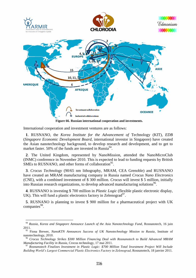
116
Figure 66. Russian international cooperation and investments.
International cooperation and investment ventures are as follows:
1. RUSNANO, the Korea Institute for the Advancement of Technology (KIT), EDB
(Singapore Economic Development Board, international investor in Singapore) have created
the Asian nanotechnology background, to develop research and development, and to get to
market faster. 50% of the funds are invested in Russia94
.
2. The United Kingdom, represented by NanoMission, attended the NanoMicroClub
(INMC) conference in November 2010. This is expected to lead to funding requests by British
SMEs to RUSNANO, and other forms of collaboration95
.
3. Crocus Technology (90/65 nm lithography, MRAM, CEA Grenoble) and RUSNANO
have created an MRAM manufacturing company in Russia named Crocus Nano Electronics
(CNE), with a combined investment of $ 300 million. Crocus will invest $ 5 million, initially
into Russian research organizations, to develop advanced manufacturing solutions96
.
4. RUSNANO is investing $ 700 million in Plastic Logic (flexible plastic electronic display,
UK). This will fund a plastic electronics factory in Zelenograd97
.
5. RUSNANO is planning to invest $ 900 million for a pharmaceutical project with UK
companies98
.
94
Russia, Korea and Singapore Announce Launch of the Asia Nanotechnology Fund, Rosnanotech, 16 juin
2011. 95
Fiona Brewer, NanoKTN Announces Success of UK Nanotechnology Mission to Russia, Institute of
nanotechnology, 2010. 96
Crocus Technology Strikes $300 Million Financing Deal with Rosnanotech to Build Advanced MRAM
Manufacturing Facility in Russia, Crocus technology, 17 mai 2011. 97
Rosnanotech Finalizes Investment in Plastic Logic: $700 Million Total Investment Project Will Include
Building World’s Largest Commercial Plastic Electronics Factory in Zelenograd, Rosnanotech, 18 janvier 2011.
117
6. Rosnanotech; in collaboration with the American Business Association of Russian-
speaking professionals AMBAR99
, brought US venture capital firms to Moscow in May
2010,.
RUSNANO opened an office in Silicon Valley to organize collaborations with American
venture capital, high-tech companies, universities and technology transfer centers100
.
7. The Finland government-owned Suomen Sijoitus Teollisuus Oy (Finnish Industry
Investment Ltd.) investment company and RUSNANO have signed a 3-year, € 50 million,
nanotechnology investment agreement on a Finnish-Russian program101
.
8. RUSNANO and Celtic Pharma Holdings (investment funds, Great Britain) have created
the Pro Bono Bio international Russian biopharmaceutical company. The total amount of
money that can be invested by RUSNANO is $ 300 million102
.
9. A technology transfer project with a Chinese company Thunder Sky Group is among the
projects funded by RUSNANO. A large-scale production of lithium-ion batteries for cars and
buses was expected to be set up in Russia103
.
10. The I2BF-RNC (Rusnano Capital Tech: RNC) strategy to fund nanotechnology
companies and facilitate the transfer of production sites in Russia was launched. I2BF is a
New York venture capital firm which invests globally104
.
11. Joint investment between RUSNANO and Domain MedInvest Associated (US venture
capital company) in California’s Coda Therapeutics pharmaceutical company (treatment of
wounds and inflammation), to install pharmaceutical and medical devices for advanced
production of therapeutic products in Russia meeting GMP standards105
.
12. RUSNANO co-invested in Business Development Lilliputian VP to establish the R&D
facility and manufacture the product in Moscow. The USB MPS is a lightweight, portable
device that can recharge a variety of electronic products, providing true wireless mobility106
.
13. RUSNANO has invested in Mapper Lithography, developer of maskless lithography
equipment. Beside expanding existing infrastructure in the Netherlands, part of the
RUSNANO investment will be used to establish a production site in Russia for Mapper lens
components107
.
98
Rosnanotech plans $900 million pharmaceutical project with British business, RIA Novosti, 25 novembre
2011. 99
US Venture Capitalists Discover Nanotechnology in Russia, Nanowerk News, 24 avril 2010. 100
RUSNANO Opens Office in Silicon Valley, Rusnano, 24 mars 2011. 101
Finland and Russia to cooperate in nanotechnology investment, Industry Investment, 27 mai 2010. 102
Rosnanotech and Celtic Pharma Holdings (Great Britain) Establish International Pharmaceutical Company
Pro Bono Bio, Rosnanotech, 12 septembre 2011. 103
Russian Nanotechnology R&D: Thinking big about small scale science, FOI Swedish Defence Research
Agency, Fredrik Westerlund, juin 2011. 104
I2BF And RUSNANO Capital Announce Strategic Nanotechnology Resources Fund, Rusnano Capital, 18
juillet 2012. 105
RUSNANO and Domain Associates Announce First Joint Investment, Rusnanotech, 25 juillet 2012. 106
RUSNANO Leads Investment in Lilliputian Systems' $60 Million Equity Financing, Rusnano, 14 septembre
2012. 107
RUSNANO Invests in MAPPER Lithography, Developer of Groundbreaking Maskless Lithography
Equipment, Rusnano, 23 août 2012.
118
14. RUSNANO has invested in Beneq, the Finnish pioneer and world leader in industrial
production and laboratory equipment for nano-scale thin films and functional coatings108
.
15. RUSNANO has taken equity in NeoPhotonics Corporation, a leading designer and
manufacturer of photonics integrated circuit. The company is expected to establish research
and production facilities in Russia109
.
16. RUSNANO has taken equity in Magnisense, a French developer of in-vitro bioassays for
diagnostic tests in health care, veterinary medicine, food safety and environmental protection.
The new project will allow Russia to manufacture an advanced diagnostic system based on
MIAtek's proprietary Magnisense110
technology.
17. EADS, a global leader in aerospace and defense, grants technology licenses to
RUSNANO by111
.
18. RUSNANO has created an international nanotechnology award in the Nano electronics,
nanobiotechnology, nanomaterials and Nanodiagnostic fields112
.
The list above is just a sampling of the many actions carried out by Russia in many countries
(India, Israel, etc.).
Since 2010, Rosnanotech no longer simply help develop Russian nanotechnology
companies, but also takes equity in high-potential foreign companies to build production
facilities in Russia with their support.
In 2012, Rosnanotech adopted a new strategy. It now co-invests with foreign funds in
foreign companies to build production facilities in Russia.
While Rosnanotech targets nanotechnology companies, it invests in diverse and strategic
areas: medical, semiconductor, solar cell, etc. This agency became close to the United States
in 2012.
Russia has been acquiring strategic technology while de-industrializing other
countries.
108
RUSNANO Invests in Beneq, Rusnano, 12 avril 2012. 109
NeoPhotonics Receives Strategic Investment from RUSNANO, NeoPhotonics, 30 août 2012. 110
RUSNANO and France's Magnisense to Produce Diagnostic Systems in Russia, Rusnano, 6 février 2012. 111
EADS and RUSNANO to Join Forces in the Nanotechnology Field, Rusnano, 27 octobre 2011. 112
Rusnano creates 'Nanotechnology International Prize' award, Rusnano, 25 mars 2009.
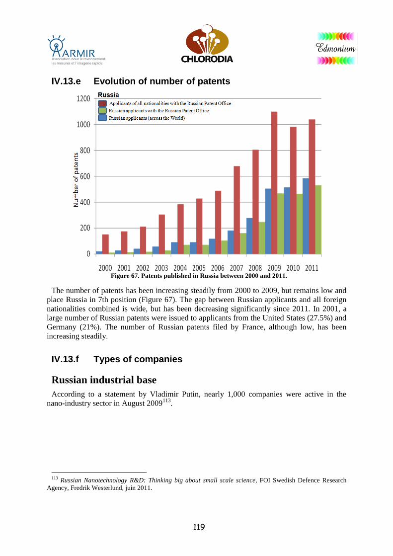
119
IV.13.e Evolution of number of patents
Figure 67. Patents published in Russia between 2000 and 2011.
The number of patents has been increasing steadily from 2000 to 2009, but remains low and
place Russia in 7th position (Figure 67). The gap between Russian applicants and all foreign
nationalities combined is wide, but has been decreasing significantly since 2011. In 2001, a
large number of Russian patents were issued to applicants from the United States (27.5%) and
Germany (21%). The number of Russian patents filed by France, although low, has been
increasing steadily.
IV.13.f Types of companies
Russian industrial base
According to a statement by Vladimir Putin, nearly 1,000 companies were active in the
nano-industry sector in August 2009113
.
113
Russian Nanotechnology R&D: Thinking big about small scale science, FOI Swedish Defence Research
Agency, Fredrik Westerlund, juin 2011.
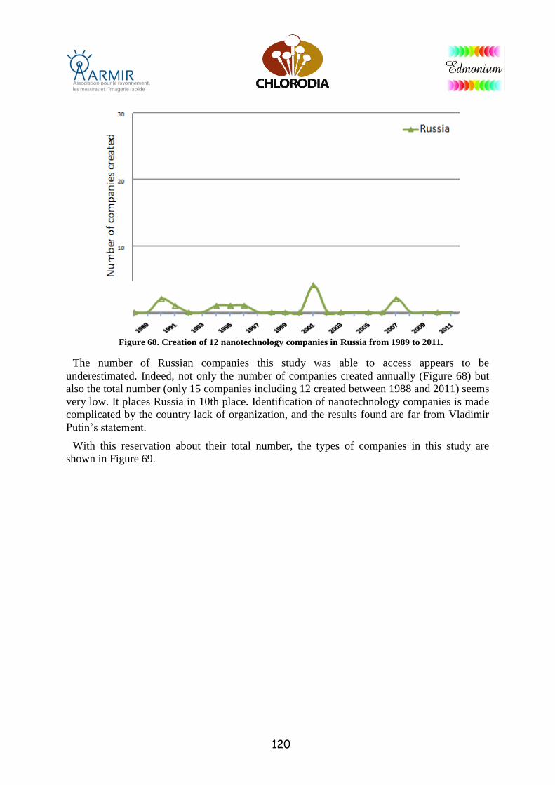
120
Figure 68. Creation of 12 nanotechnology companies in Russia from 1989 to 2011.
The number of Russian companies this study was able to access appears to be
underestimated. Indeed, not only the number of companies created annually (Figure 68) but
also the total number (only 15 companies including 12 created between 1988 and 2011) seems
very low. It places Russia in 10th place. Identification of nanotechnology companies is made
complicated by the country lack of organization, and the results found are far from Vladimir
Putin’s statement.
With this reservation about their total number, the types of companies in this study are
shown in Figure 69.
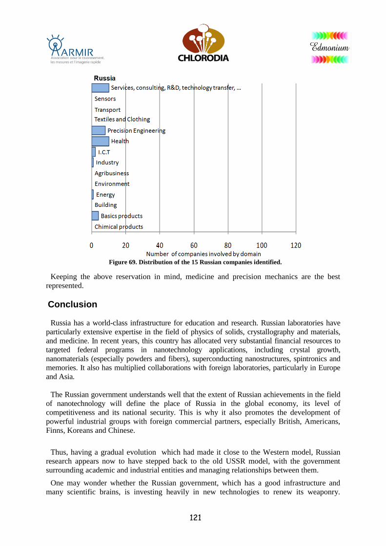
121
Figure 69. Distribution of the 15 Russian companies identified.
Keeping the above reservation in mind, medicine and precision mechanics are the best
represented.
Conclusion
Russia has a world-class infrastructure for education and research. Russian laboratories have
particularly extensive expertise in the field of physics of solids, crystallography and materials,
and medicine. In recent years, this country has allocated very substantial financial resources to
targeted federal programs in nanotechnology applications, including crystal growth,
nanomaterials (especially powders and fibers), superconducting nanostructures, spintronics and
memories. It also has multiplied collaborations with foreign laboratories, particularly in Europe
and Asia.
The Russian government understands well that the extent of Russian achievements in the field
of nanotechnology will define the place of Russia in the global economy, its level of
competitiveness and its national security. This is why it also promotes the development of
powerful industrial groups with foreign commercial partners, especially British, Americans,
Finns, Koreans and Chinese.
Thus, having a gradual evolution which had made it close to the Western model, Russian
research appears now to have stepped back to the old USSR model, with the government
surrounding academic and industrial entities and managing relationships between them.
One may wonder whether the Russian government, which has a good infrastructure and
many scientific brains, is investing heavily in new technologies to renew its weaponry.
122
Indeed, the civil / military ambivalence of nanotechnology can make military developments
look like a legitimate approach to civilian application in order to revitalize the economy. The
new innovation support structures also are a clear strategic military asset:
- Rosnanotech helps to foster links with foreign countries and to transfer advanced
technologies to Russia.
- The various international fairs provide the opportunity for Russia to gather information
about research topics in other countries.
- Partner-finding tools such as RTT or RFR 114
allow research centers and their skills to be
mapped.
- Collaboration with foreign countries bring new know-how.
All the institutions which help technology transfer, together with the ambivalent
character of “defense,” can promote renewal of armament to restore military power, and
thus credibility as a world power.
114 RFR: Réseau Franco-Russe de Centres d’Innovation Technologique aims to offer a communication tool between Russian and French
companies and transfer technologies organizations, so that they can share offers and requests for technology partnerships through a website (www.rfr-net.org).
RTTN: the Russian Technology Transfer Network was founded in 2002. It is an association of 68 Russian innovation centers from the 25
regions of Russia and CIS labeled Technology Transfer Areas. The RTTN is a tool for the effective dissemination of technological information as well as for finding partners for the implementation of innovative projects. The Russian Technology Transfer Network is a
project initiated by the Obninsk Regional Innovation Technological Centre (RMCT Obninsk) and the Koltsovo's Innovation Centre (ICK)
under the TACIS program (Project 9804 FINRUS) (www.rttn.ru).
123
IV.14 Taiwan
IV.14.a Master data
Population (2010) 23 millions
Area 36,008 sq. km
Average population density 640 residents/sq. km
GDP (2011) $ 504.5 billon
GDP/inhabitant (2011) $ 37,932
HDI (2011) 0.868
IV.14.b Taiwan’s efforts
Taiwan, like mainland China, has made nanotechnology a priority area, supporting this sector
of activity with many public investments. While mainland China’s priorities are focused on
nanomaterials, Taiwan has focused on semiconductors115
. Taiwan’s interest for this area
comes from its perception that nanotechnology is a research-stimulating factor. This analysis
is part of a broader vision of future commercial success, competitiveness and economic
growth of the country.
Taiwan remains a very active nation in nanotechnology research116
and is among the world's
top countries in basic research117
. Research is facilitated by access to world-class
characterization infrastructure, such as the National Synchrotron Radiation Research Center
(NSRRC).
Since 2003, Taiwan has been investing significant resources in the development of
nanotechnology through two programs, with a view to finding industrial outlets:
In late 2002, the Taiwanese authorities launched a wide-ranging nanotechnology
development program called Taiwan National Science and Technology Program for
Nanoscience and Nanotechnology (NNP). This program, amounting to over one billion euros
has, in its first phase (2003-2008), developed academic capabilities in a dozen laboratories
and research agencies and then, during the second phase (2009-2014), supported development
of applications.Taiwan has also set up a National Program on Nanoscience and technology,
with a budget of about $ 670 million, from 2003 to 2008, around $ 110 million per year, with
the following main themes:
Basics research on the physical, chemical and biological properties of nanostructures,
Synthesis, assembly and processing of nanomaterials,
Development of manipulation techniques and fabrication of functional nanodevices,
Energy related nanotechnology,
115
Bulletin économique Chine, Publications des Services économiques, Trésor D G, N°41 November 2011. 116
Both academically and in government laboratories and in private industry. 117
Defense Nanotechnology Research and Development Program, Department of Defense, December 2009.
124
Nano-biotechnology 118
.
Based on the first phase results, the authorities decided, after 2009, to accelerate the shift to
industrial applications, with the support of a coordination structure led by the Academia
Sinica, through the National Nanotechnology Bridge Program.
In 2010, leaders of the NNP program estimated that every dollar invested by the government
for industrialization of nanotechnology program had generated $ 1.5 private investment, and
the production value of Taiwan's nanotechnology products would more than double between
2012 and 2015, from $4 to 10 billion.
With the second phase of NNP (2009-2014), Taiwan also began to be interested in
environmental, health and safety issues and standardization work by earmarking 30% of the
amount allocated to strategic projects (nearly 17 million $).
The program revolves around the following themes 119
:
Academic Excellence, Research Program: Basic research on nanoscience, Synthesis,
assembly and processing of Nanomaterials, Development of manipulation techniques
and fabrication of functional nanodevices, Nano-biotechnology, Energy
applications.Education Program.
Core Facilities Program.
Nanotechnology Industrialization Program: To enhance core facility and network, To
speed up the development of nanotechnology, To develop and apply novel properties
of nano-materials, To leverage the existing industrial knowledge and create new
opportunities, To integrate new technical findings into the most competitive
technologies and industries in Taiwan.Furthermore, the Taiwanese Ministry of the
Economy created in 2004 the Nanomark quality label to protect, on the one hand, consumers
against products improperly claiming a nanotechnology content and, on the other hand,
companies against unfair competition.
Finally, Taiwan is among the Top 15120
of the world’s major nanotechnology research center
clusters, ranking 14th (see Figure 30).
The most significant Taiwanese research centers working on nanotechnology include
Academia Sinica, National Taiwan University, National Tsing Hua University, the Industrial
Technology Research Institute (ITRI) and the NSRRC synchrotron. The success of the
Taiwanese management strategy is based on knowledge management, human capital and
technological production.
118
Nanoscience & Nanotechnology Research Program in Taiwan, Maw-Kuen Wu Director, Institute of
Physics, Academia Sinica, Taipei, Taiwan and NNNP, TWAS 10th General Conference, 6 septembre 2006. 119
2011科技政策與創新前瞻研討會, Performance Measure and Efficiency Analysis of National Priority
Science and Technology Programs in Taiwan, 台灣經濟研究院, 2011年6月7日. 120
Source: extract from L'internationalisation des systèmes de recherche en action. Les cas français et Suisse,
Ph. Laredo, J.-Ph. Leresche et K. Weber (Ed.), 2009, 24 p.
125
IV.14.c Priority sectors.
Overall, the Taiwanese industry is mainly based on high technology, key sectors being:
Automotive et auto parts;Biotechnology;Photovoltaics;
Renewable energies;
Nanotechnologies;
Semiconductors;
Laptops;
Communication and networks;
GPS;
Petrochemicals;
Machinery;
Maritime transportation;
Yachts;
Bicycles.
With respect to nanotechnologies, Taiwanese researchers excel in the following areas:
nanofabrication and synthesis;
characterization techniques;
nano-bio devices;
environment-health-safety;
standardization work.
IV.14.d Defense and security-related programs
Taiwan mainly focuses its research on nano-optoelectronics, which offers many Defense
opportunities exist and which can be displayed at the annual AFOSR fair121
. However,
information on defense-related activities is not easily accessible.
121
Taiwanese Air Force.
126
IV.14.e Evolution of number of patents
Figure 70. Patents issued in Taiwan between 2000 and 2011.
Taiwan ranks 6th in terms of patents filed, among the 13 countries in this study. But there is
a significant gap between the number of Taiwanese applicants and of all other nationalities
(Figure 70). This can be explained by the fact that Taiwanese companies rely on internal
developments based on national and international cooperation 122
. The number of patents has
grown steadily between 2000 and 2009. Filings by Taiwanese nationals did not start in earnest
before 2004. This date matches the creation of the Taiwan National Science and Technology
Program for Nanoscience and Nanotechnology (NNP). The program was dedicated to
academic research for the years 2003 to 2008. Patent applications by Taiwanese are probably
issued by academic research agencies and laboratories.
IV.14.f Types of companies
From the table below, it appears that Taiwan mainly attempts to acquire skills through
international cooperation, and seems to emphasize very little its domestic R&D expertise.
122
Status of the Nano-technology and Applications in Taiwan, Department of Invesment Services, MOEA,
2012.
127
Figure 71. Nanotechnology Development Strategy in Taiwan.
The total number of identified companies appear to be particularly low (15 companies), and
does not necessarily correspond to reality (Figure 72).
128
Figure 72. Creation of 9 nanotechnology companies in Taiwan from 1989 to 2011.
15 companies have been identified, including 9 created between 1988 and 2011. There was
some activity, beginning in 2003, which corresponds to the government's investment at the
time, then very low activity became non-existent in 2009. The second phase of the Taiwan
National Science and Technology Program for Nanoscience and Nanotechnology (NNP),
from 2009 to 2014, dedicated to industrial development, appears to not yet have had the
desired effects on nanotechnology company creation.
Development of nanotechnology in Taiwan has been bootstrapped by the
semiconductor industry. Companies created are representative of this investment by the
electronic component industry123
. In terms of income and investment figures, large electronics
companies (TSMC, ASE, UMC, Mediatek, SPIL, etc.) account for the bulk of the activity
(97% of investments in 2007). In terms of number of companies, the traditional sector (paint,
textiles, ceramics, metal, mechanical engineering, paper) is the most represented (70% of
existing companies), but it accounts for only a small share of nanotechnology investments.
With the abovementioned reservation about number, types of Taiwanese companies are
shown in Figure 73.
123
For example, in 2011, TSMC has started production of 28nm semiconductors (for this production, the
company was awarded the Green Classic Award by the Ministry of Economy).
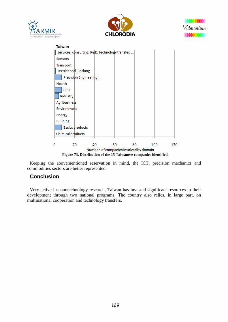
129
Figure 73. Distribution of the 15 Taiwanese companies identified.
Keeping the abovementioned reservation in mind, the ICT, precision mechanics and
commodities sectors are better represented.
Conclusion
Very active in nanotechnology research, Taiwan has invested significant resources in their
development through two national programs. The country also relies, in large part, on
multinational cooperation and technology transfers.
130
Conclusion
Nanotechnologies are a key element of future technologies. They are the natural evolution of
microtechnology and allow progress to be achieved in all areas. Not to be significantly present
in this field would lead to becoming dependent of the countries which will master these
technologies. It would also contribute to de-industrialization of France, thus also increasing
even more its dependency to other industrial powers. This is true for the civilian sector, and
this also true in the field of defense.
This study shows that competition in the field of nanotechnologies is global and robust.
France needs a collective approach to research, rather than scattering our resources. To be
internationally competitive, a critical mass in the three nanotechnologies key areas is
necessary: characterization, modeling / simulation and manufacturing. Technology centers are
a big step to that end, and that effort must be amplified.
To irrigate the industrial base commercializing what research has achieved, a chain from
basic research to applications and technology transfer is necessary. Each link must be closely
connected to the previous and the next ones. Government initiatives must promote and help
this linking. Basic research must enjoy creative freedom, because no one knows what will be
needed tomorrow, and innovations cannot be programmed. Applied research should focus on
activities allowing industrial development, through strong links between laboratories and
industry, through adequate funding at all stages of development, especially to support the
growth of start-ups.
In terms of international competition, the speed of innovation is critical.
In this study, we have tried to identify for 12 countries and France, scientific and
technological skills, and industrial capacities, in various sectors where nanotechnologies are
present. We have focused on the ten having a strong potential the development of military or
security applications.
With respect to for France, one can be optimistic. Government efforts in the last ten years
are beginning to bear fruit, and this is expected to continue in the coming years. Concentration
in one place of education, research and industrial facilities is essential to prepare for the
future. This is what is taking place in the Major Technology Centers. However, one should be
aware that there is still a long and difficult path forward, and that evolution is slow. There are
often thirty years between a research result and products available in stores. Patience and
perseverance are necessary.
This conclusion is a brief summary of the report with some general remarks. A detailed conclusion, and
several recommendations as well as an analysis of the situation of nanotechnologies in France and the 12 other
countries studied are available in the restricted version of this report.
131
Annexe 1 : Germany
Appendice 1 : Fraunhofer Alliance Nanotechnologie Nanomaterials / nanochemistry
IAP
Fraunhofer-Institut für Angewandte Polymerforschung in Golm Tissue, cells, blood cells - biological material provides numerous models for polymeric nanosystems. Synthetic polymers designed according to biological construction principles are therefore excellent carrier for active pharmaceutical ingredients (drug carrier). By providing these polymeric nanoparticles with specially tailored surfaces and structures, they can be directed to specific sites in the body (drug targeting). Nanocomposites are a new material class in the plastics sector that will decisively influence material adaptation and material optimization in the future. Polymeric nano- or microparticles of uniform shape and size, such as are obtained by emulsion polymerization, can be organized into highly ordered, crystal-like structures. Birefringent film components with light-modulating properties are key elements in display technology or technology fields such as sensor technology or optical measuring technology. Block copolymers are the basis for macroscopically homogeneous polymer alloys with a nanoscale sub-structure. Details of the Institute's expertise
ICT
Fraunhofer-Institut für Chemische Technologie in Pfinztal Powder particles, particles or structures having dimensions within the nanometer range are the center of attention of the interdisciplinary nano technology at the ICT. Details of the Institute's expertise
IFAM
Fraunhofer-Institut für Fertigungstechnik und Angewandte Materialforschung in Bremen Most of IFAM's activities in the area of nano technology concern the interface between the surface of the nanoparticles and the polymer matrix. These activities include the manufacture of metallic nanoparticles, the surface modification of a wide range of nanoparticles, the compounding of nanoparticles with matrix polymers and the characterisation of nanocomposites right through to the development of new analytical methods. Other key areas of work concern surface and thin film technology and relevant analysis. Details of the Institute's expertise
IKTS
Fraunhofer-Institut für Keramische Technologie und Strukturkeramik in Dresden
Sub-µm-and nano-technologies for transparent ceramic components exhibiting highest strength, hardness and wear resistance together with an extreme thermal and chemical stability Details of the Institute's expertise
ISC
Fraunhofer-Institut für Silicatforschung in Würzburg
The main focus of the Fraunhofer ISC is the production of nanomaterials. The sol-gel technology plays an important role for the manufacture of inorganic nano-scaled structure e.g. antireflex coating of glasses and the production of interference filters. Another nanomaterial are the inorganic-organic hybrid polymers (ORMOCER
®e). With these polymers nano-scaled structures for microelectronic could be produced. Besides permeable
hollow fibers inorganic hollow fibers (SiO2) with nanopores can also be fabricated, which show high gas separation. Functionalized nanoparticles as filler and carrier material complete the nano-scaled material range. Details of the Institute's expertise
IVV
Fraunhofer-Institut für Verfahrenstechnik und Verpackung in Freising
The Fraunhofer IVV carries out R&D work on plastic packaging materials for food and pharmaceutical products and technical applications. The main focus of these activities is on developing and characterizing flexible polymer films which possess barrier properties or active additional functions. Our expertise includes film manufacture and conversion as well as carrying out tests on material properties such as permeation measurements and mechanical parameters. Details of the Institute's expertise
IWM
Fraunhofer-Institut für Werkstoffmechanik in Halle and Freiburg i. Br. The main emphasis of IWM Halle and Freiburg in nanotechnology lies in the development and qualified use of functionalized nano structured materials for biotechnology such as nano-structuring by microsystem focussed ion beam techniques and surface functionalization of nanoporous membrane layers by enzymes. Details of the Institute's expertise
IWS
Fraunhofer-Institut für Werkstoff- und Strahltechnik in Dresden
With respect to thin films produced by PVD, CVD or laser processing, our scientists have a wide range of experiences. The nanostructuring of tetragonal-amorphous carbon films by Scanning Transmission Microscopy (STM) enables, e.g., information storage with extremely high storage density up to > 10.000 Gb/in2 and extreme long-term stability. Details of the Institute's expertise
Nanooptics / nanoelectronics
ENAS
Fraunhofer-Institut für Elektronische Nanosysteme in Chemnitz The Fraunhofer Institute for Electronic Nano Systems ENAS in Chemnitz focuses on research and development in the field of smart systems integration by using micro and nano technologies together with partners in Germany and overseas, especially in Europe and Asia. Derived from the future needs of the industry Fraunhofer ENAS focuses on high precision silicon MEMS und NEMS (micro electro mechanical system und nano electro mechanical system), polymer based low-cost systems, RF MEMS, MEMS/NEMS design, development and test, wafer level packaging of MEMS and NEMS, green and wireless systems, metallization and interconnect systems for micro and nano electronics as well as 3D integration, process and equipment simulation, reliability and security of components and systems, printed functionalities. Details of the Institute's expertise
IISB
Fraunhofer-Institut für Integrierte Systeme und Bauelementetechnologie in Erlangen A technology which is used and enhanced besides the conventional lithographic structuring methods is based on the application of ion- and electron beams in a scanning force probe. Details of the Institute's expertise
ISE
Fraunhofer-Institut für Solare Energiesysteme in Freiburg
The Fraunhofer ISE is engaged in the field of organical and dye solar cells with new concepts and production technologies as further developments this novel photovoltaic converter. Besides the comprehension of optical absorption- and electrical transport processes is a matter of the further

132
development of nano scaled semiconductor materials and the conception of light management of microstructures. These concepts could be transformed to the field of displays. Another focus is the investigation of optically variable layer systems based on electro- and photo-chromatic material systems. Besides the basic research on these systems production technologies will be developed for large area manufacturing with these systems. Overview | Details "Dye- and Organic Solar Cells" Details "Material development " | Details "Nanostructured Device Architectures"
Nanoprocessing / handling
IFF
Fraunhofer-Institut für Fabrikbetrieb und -automatisierung in Magdeburg
Starting from the know-how already available and the experience in classical robotics, sensor technology and development of very fast controllers, new drive systems and tools for precision positioning up to the nanometer range are developed. Details of the Institute's expertise
ILT
Fraunhofer-Institut für Lasertechnik in Aachen Laser and photon-based processes play an ever-increasing role in the production of nanotechnology products and lead to more flexible, cost-effective manufacturing solutions. Examples are laser processing of nanoparticulate films, the production of deterministic periodic surface structures by multibeam interference, multi-photon nano-drilling as well as lithography with extreme ultraviolet (EUV) radiation. Also in the area of metrology and diagnostics, laser-based processes open up new possibilities. For example, this could be the spectral analysis of airborne nanoparticles, the measurement of film thicknesses on the nanometer scale using LIBS (Laser-Induced Breakdown Spectroscopy) or EUV microscopy. In addition, Fraunhofer ILT develops customized beam sources for nanoscale applications. These include 13 nm sources for nanolithography and high-power ultra-short pulse lasers for nanostructuring. Furthermore, ILT is active in the field of the designing and manufacturing plasmonic components for nanophotonics. Details of the Institute's expertise
IPA
Fraunhofer-Institut für Produktionstechnik und Automatisierung in Stuttgart As your partner for contract research we develop and optimise solutions for different tasks in engineering sciences. In the range of coating technologies processes with high process reliability and reproducibility in coordination between material development and coating process are formed. Thereby planning, developments, modelling and simulations up to implementations suitable for production are in the front. Details of the Institute's expertise
Nanobiotechnology
IGB
Fraunhofer-Institut für Grenzflächen- und Bioverfahrenstechnik in Stuttgart
The Fraunhofer Institute for Interfacial Engineering and Biotechnology IGB offers R&D solutions in the fields of health, environment and technology. Our competences comprise interfacial engineering and membrane technology as well as biotechnology, cell biology and bioprocess engineering. We offer solutions from market analysis through research & development until the finished product. Details of the Institute's expertise: Cytokine-functionalized Nanocytes
®
ITEM
Fraunhofer Institute of Toxicology and Experimental Medicine ITEM in Hannover
ITEM has been investigating for more than 25 years primarily the toxic mechanisms and effects of inhaled substances in the respiratory tract. Research contracts are conducted for the pharmaceutical and chemical industry as well as for public sponsors. In the last decade, pharma research competencies have been enlarged continuously. Besides molecular (omics methods), preclinical and clinical pharma research (focus: allergy and asthma research), toxicological investigations on occupational and environmental issues and consumer protection are of crucial importance. A long-term competency is existing in the characterization and toxicological investigation of particle and fiber aerosols. For man-made mineral fibers, a standard test analyzing the biopersistence in vivo has been established. The actually discussed issue of the toxicological assessment of engineered nanoparticles has initiated a new research topic "nanotoxicology". Within the Fraunhofer nanoparticle alliance a battery of in vitro assays will be established that can help the producers to characterize rapidly and at affordable costs the toxicological potential of new nanoparticles before marketing the products. Details of the Institute's expertise
New equipment / methods
IZFP
Fraunhofer-Institut für zerstörungsfreie Prüfverfahren in Saarbrücken The department of basic science at Fraunhofer IZFP deals with new test methods to develop the error detection and characterization of modern materials, also nanomaterials for future relevant aspects. Particularly, an ultrasonic force microscope for investigating nanostructures was developed. Details of the Institute's expertise
LBF
Fraunhofer-Institut für Betriebsfestigkeit und Systemzuverlässigkeit in Darmstadt
The main competence of Fraunhofer LBF is the testing of materials, components and systems with respect to structural durability and system reliability. Therefore, it is at the end of the value added chain but it is of increasing importance to incorporate aspects of reliability into nanomaterials already at an early stage. Details of the Institute's expertise
Technology transfer/ consulting
IAO
Fraunhofer-Institut für Arbeitswirtschaft und Organisation in Stuttgart The Fraunhofer IAO deals with current questions in the field of management technology. The nanotechnology holds an innovation potential for many seminal industrial applications. The environmental and power technology benefits from the tiny all-rounder. The nanotechnology offers various possibilities of application, e.g. supply of drinking water, saving of valuable resourses and climate protection. Details of the Institute's expertise
ISI
Fraunhofer-Institut für System- und Innovationsforschung in Karlsruhe Relevant to industry, relevant to society – the Fraunhofer Institute for Systems and Innovation Research ISI investigates how technical and organizational innovations shape industry and society today and in the future. A trademark of the systemic approach is the integration of research disciplines and the construction of a network for innovations, together with clients and interested parties. With its expertise, experience and reports, ISI as one of the application-oriented research institutes in the Fraunhofer-Gesellschaft makes a contribution towards strengthening European competitiveness. For this reason, politicians, associations and enterprises utilize Fraunhofer ISI as a foresighted and neutral intellectual mastermind able to convey visions for decisions. Details of the Institute's expertise
133
Appendice 2 : Specialized Agencies and Competence
Networks
- DFG: resources for research agency.
- WGL: Leibniz Association of Community Centers, with the main institutes: Institut für
Neues Materialien (INM) -Saarbrücken, Institut für und Festkörper Werkstoffforschung
(IFW) -Dresden Institute for Polymer Research (IPF) -Dresden, Institut für
Oberflächenmodifizierung (IOM ) -Leipzig, the research Centre Rossendorf (FZR) -Dresden,
the Ferdinand Braun Institut für Hochfrequenztechnik (FBH) -Berlin.
- HGF: Community of the Helmholtz centers (Defence), Research Centre Jülich and
Karlsruhe-FZK-FZJ Research Center in Geesthacht GKSS-.
- MPG: Max Planck Society, with institutes Institut für Festkörperforschung - Stuttgart,
Institut für Metallforschung -Stuttgart, Institut für Mikrostrukturphysik - Halle Institute for
Polymer - Mainz.
- FhG: Fraunhofer Society, which brings together twenty of its institutions (Annex 1) on the
following topics: nanomaterials / Nanochemistry - nanooptics / nanoelectronics -
nanoprocessing / handling - nanobiotechnology - new equipment / methods.
- Caesar Foundation.
The "Offensive German future for nanotechnology" was devoted to this subject (launched in
2004). Based on intensive discussions with representatives of business and science, the
objective of the support of the BMBF nanotechnology is to identify potential application by
using research cooperation (declined in guiding Innovations) strategically oriented chain of
value creation, and to avoid the imminent shortage of experts in relation to the level of
education policy. For a large number of important industrial sectors in Germany, the future
competitiveness of their products also depends on the development of nanotechnology and the
disposal of the company to use these products. The lively dialogues by the BMBF on the
opportunities and the risks taken at the ecological, health, social and policies are taken into
account to ensure public relations open. Since the late 80s, the BMBF supports research in the
field of nanotechnology in the programs "Materials Research" and "Physical Technologies."
The focus was primarily on the preparation of nanopowders on achieving lateral structures on
silicon and on the development of nano-analytical methods. The BMBF has also supported
research in the context of other programs such as "The laser research" and "Optoelectronics".
These supports are now deployed in all sectors of German industry, such as nanomaterials,
production technologies, optical technologies, microsystems Techniques, Communication
Technologies, nanoelectronics, nanobiotechnology, technical analysis and innovations, etc.
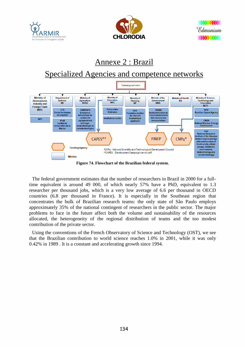
134
Annexe 2 : Brazil
Specialized Agencies and competence networks
Figure 74. Flowchart of the Brazilian federal system.
The federal government estimates that the number of researchers in Brazil in 2000 for a full-
time equivalent is around 49 000, of which nearly 57% have a PhD, equivalent to 1.3
researcher per thousand jobs, which is a very low average of 6.6 per thousand in OECD
countries (6.8 per thousand in France). It is especially in the Southeast region that
concentrates the bulk of Brazilian research teams: the only state of São Paulo employs
approximately 35% of the national contingent of researchers in the public sector. The major
problems to face in the future affect both the volume and sustainability of the resources
allocated, the heterogeneity of the regional distribution of teams and the too modest
contribution of the private sector.
Using the conventions of the French Observatory of Science and Technology (OST), we see
that the Brazilian contribution to world science reaches 1.0% in 2001, while it was only
0.42% in 1989 . It is a constant and accelerating growth since 1994.
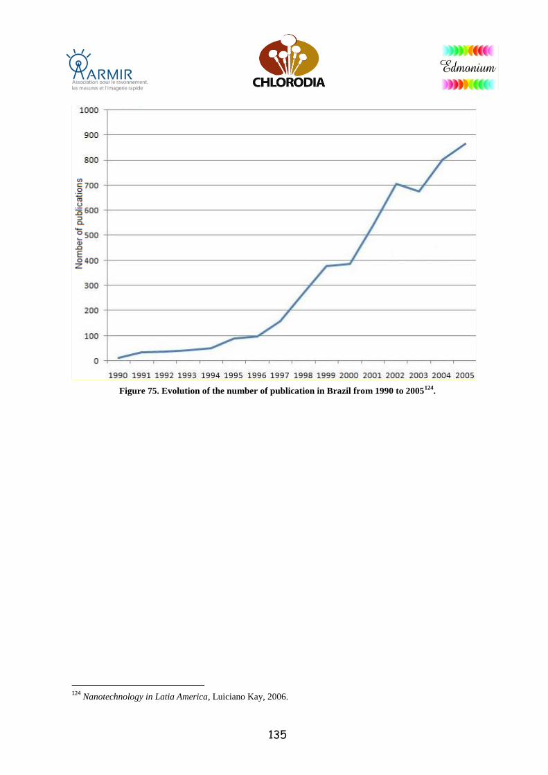
135
Figure 75. Evolution of the number of publication in Brazil from 1990 to 2005124
.
124
Nanotechnology in Latia America, Luiciano Kay, 2006.

136
University of Campinas UNICAMP: LNLS
Synchrotron Laboratory, Laboratory
nanotechnology and solar energy laboratory on
nanostructures and interfaces laboratory dielectric
materials / optical and nanocomposites
Campinas www.lnls.br
www.ccs.unicamp.b
r/namitec
University of Sao Paulo: nanotechnologies and
nanomaterials
Sao
Paulo
www.usp.br/prp/na
notecnologia/
Agricultural research center EMBRAPA: national
laboratory of nanotechnology in agriculture
Sao Carlos, www.embrapa.br/en
glish
Federal University of Rio de Janeiro: Instituto
de Biofísica, Instituto de Física, Instituto
de Macromoléculas, Instituto
de Química e Programa de Pos-
Graduação e Pesquisa de Engenharia COPPE. Cop
pe et l'Instituto deMacromoléculas
Rio
de Janeiro
INMETRO specialized in metrology and
standardization of nanotechnology
Rio
de Janeiro
www.inmetro.gov.br
Catholic University: multidisciplinary
nanotechnology (physics, electrical engineering,
chemistry, computer science, materials science,
mathematics)
Rio
de Janeiro
www.ica.ele.puc-
rio.br/nanotech/main.
asp
Federal University of Minas Gerais: carbon
nanotubes and nanotechnology for aerospace
industry ; the Chemistry Institute
Rio
de Janeiro
www.ufmg.br/engli
sh
Federal University of Pernambuco UFPE:
Nanophotonics and nanomolecules
Recife-
Pernambuco
www.ufpe.br
Federal University of Amazonas UFAM:
nanobiotechnology and nanoelectronics NEMS
Manaaus www.ufam.edu.br
www.suframa.gov.b
r/minapim
Figure 76. Major Brazilian nanotechnology research centers.
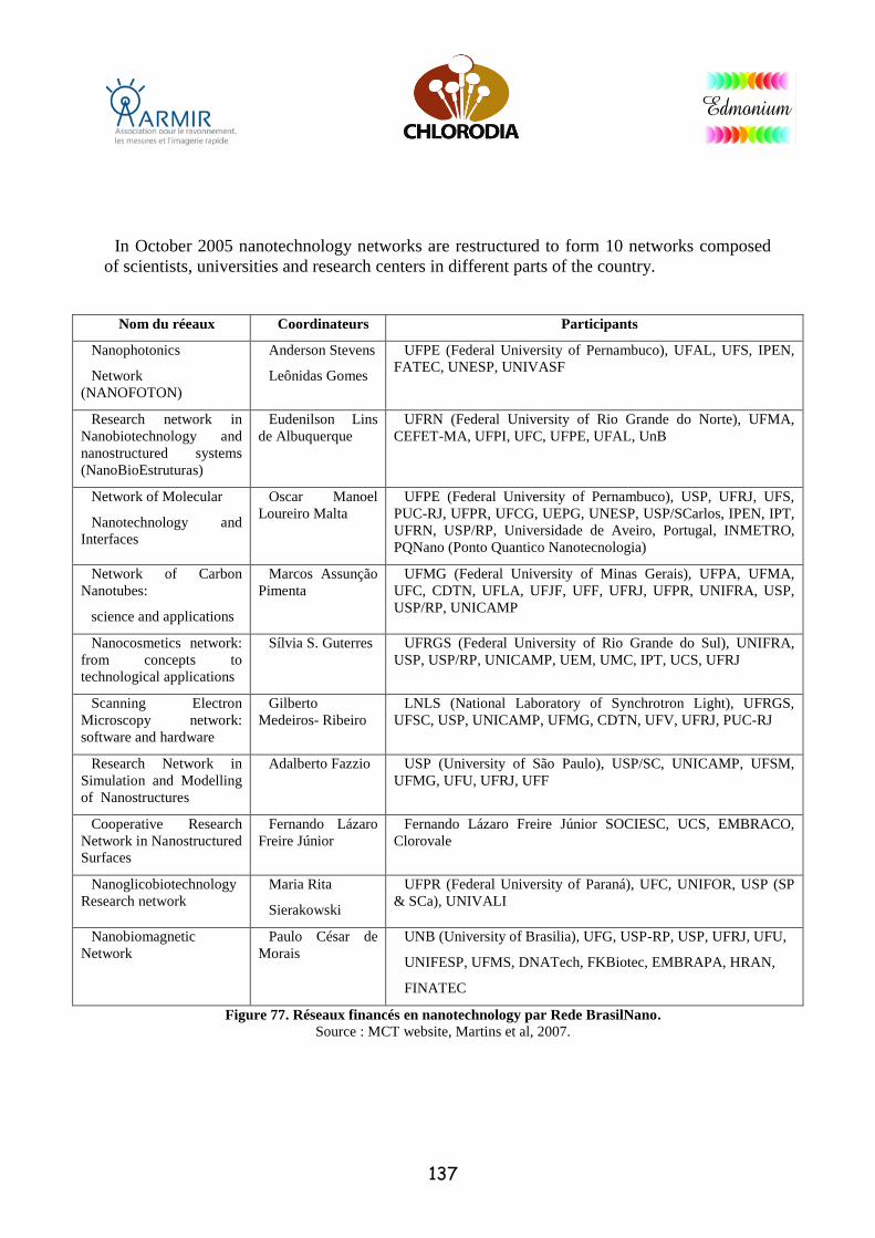
137
In October 2005 nanotechnology networks are restructured to form 10 networks composed
of scientists, universities and research centers in different parts of the country.
Nom du réeaux Coordinateurs Participants
Nanophotonics
Network
(NANOFOTON)
Anderson Stevens
Leônidas Gomes
UFPE (Federal University of Pernambuco), UFAL, UFS, IPEN,
FATEC, UNESP, UNIVASF
Research network in
Nanobiotechnology and
nanostructured systems
(NanoBioEstruturas)
Eudenilson Lins
de Albuquerque UFRN (Federal University of Rio Grande do Norte), UFMA,
CEFET-MA, UFPI, UFC, UFPE, UFAL, UnB
Network of Molecular
Nanotechnology and
Interfaces
Oscar Manoel
Loureiro Malta UFPE (Federal University of Pernambuco), USP, UFRJ, UFS,
PUC-RJ, UFPR, UFCG, UEPG, UNESP, USP/SCarlos, IPEN, IPT,
UFRN, USP/RP, Universidade de Aveiro, Portugal, INMETRO,
PQNano (Ponto Quantico Nanotecnologia)
Network of Carbon
Nanotubes:
science and applications
Marcos Assunção
Pimenta UFMG (Federal University of Minas Gerais), UFPA, UFMA,
UFC, CDTN, UFLA, UFJF, UFF, UFRJ, UFPR, UNIFRA, USP,
USP/RP, UNICAMP
Nanocosmetics network:
from concepts to
technological applications
Sílvia S. Guterres UFRGS (Federal University of Rio Grande do Sul), UNIFRA,
USP, USP/RP, UNICAMP, UEM, UMC, IPT, UCS, UFRJ
Scanning Electron
Microscopy network:
software and hardware
Gilberto
Medeiros- Ribeiro LNLS (National Laboratory of Synchrotron Light), UFRGS,
UFSC, USP, UNICAMP, UFMG, CDTN, UFV, UFRJ, PUC-RJ
Research Network in
Simulation and Modelling
of Nanostructures
Adalberto Fazzio USP (University of São Paulo), USP/SC, UNICAMP, UFSM,
UFMG, UFU, UFRJ, UFF
Cooperative Research
Network in Nanostructured
Surfaces
Fernando Lázaro
Freire Júnior
Fernando Lázaro Freire Júnior SOCIESC, UCS, EMBRACO,
Clorovale
Nanoglicobiotechnology
Research network
Maria Rita
Sierakowski
UFPR (Federal University of Paraná), UFC, UNIFOR, USP (SP
& SCa), UNIVALI
Nanobiomagnetic
Network
Paulo César de
Morais
UNB (University of Brasilia), UFG, USP-RP, USP, UFRJ, UFU,
UNIFESP, UFMS, DNATech, FKBiotec, EMBRAPA, HRAN,
FINATEC
Figure 77. Réseaux financés en nanotechnology par Rede BrasilNano.
Source : MCT website, Martins et al, 2007.
138
Annexe 3 : South Korea
Appendice 1 : Geographical distribution of
activities
The provincial universities (excluding the regions of Seoul, Incheon, and Gyeonggi) benefit
from NURI program of KRF, which aims to strengthen regional competitiveness based on a
partnership universities, research centers, industry, NGOs and local governments. Since 2004,
the government has financed the construction of 10 regional research centers (Daejeon,
Jeanbuk, Gwangju, Chungbuk, Gangneung, Busan, Daegu ...). In 2010, these centers
receiving up to € 11 million over a maximum period of 5 years. The Daedok cluster in
Daejeon, by far the most active after Seoul, has 824 high-tech companies, including in
nanotechnology, many research institutes, universities and industries. Concentration close to
20% of the country's research effort, it generated annual revenue of 7.18 billion euros in 2010.
Gyeonggi Province (southern Seoul) account for its large number of foreign R & D
institutions, because of its proximity to the séoulite megalopolis and significant investment in
R & D by the government of the province (for France Institut Pasteur Korea, supported by the
authorities of that province, and the french company Faurecia (2nd largest automotive
equipment) for a project to create an R & D center for the development of applications for
automobiles sold in the market Korean.)
Top 5 universities (KAIST, Seoul National University, Yonsei University, POSTECH,
Korea University) emerging as major centers of scientific production in all rankings (number
of the highest scientific publications).
139
Appendice 2 : National Research and Innovation
System
The Ministry of Education, Science and Technology (MEST, formerly Ministry of Science
and Technology, MOST until the reform of March 2008) acts as secretariat for the NSTC and
acts as an inter-agency Central coordinating R & D public policies. MEST consists of two
divisions, one for science and one for technology education. MEST is the largest R & D
contributor public sector (31.9%), followed by the Ministry of Economy and Knowledge
(MKE), around 29.3%, the Ministry of Defence (15.9 %) and the Ministry of Land and
Maritime Affairs (5.2%). MEST, MKE and the Prime Minister ensure the monitoring,
evaluation and coordination of public research institutes funded by the government
(Government-sponsored Research Institutes, GRI). MEST is in charge of steering 24 GRI,
which are mostly specialized institutes into a scientific discipline. 11 of them are directly
controlled by the Ministry of Education, Science and Technology, to enable them to perform
specific tasks directly related to the mandate of the Ministry. The other 13 GRI are placed
under the supervision of the Korea Research Council of Fundamental Science & Technology
(KRCF) that ensures their control.
Authority on Universities : The Ministry of Education, Science and Technology (MEST) is
responsible for the formulation and implementation of education policies in line with the
academic and scientific activities of universities. Universities are funded at 75% by the
MEST, the remaining 25% are from local authorities and / or companies and tuition fees for
students who remain very high in Korea. The budget MEST represents 31.9% of the total
government budget in 2010 and 27.2% of its budget is spent on higher education. In 2009
Korea has about 3.5 million students of which 40 500 foreign and some 73 000 university
professors to 42 "National Universities", 10 public universities and 353 private universities.
Funding Agencies : Korea has very high ambitions in terms of science and technology with
the aim to raise the country among the top ten nations in terms of scientific output by 2012.
This policy is reflected in particular by the scale of the resources allocated to R&D in South
Korea with the objectives set at 5% of GDP by 2012. In order to increase efficiency and
visibility in the use of these means, the 3 research funding agencies under the tutelage MEST
were restructured to form the National Research Foundation (NRF), which opened June 25,
2009. There are a dozen other agencies for funding and managing research programs under
the supervision of other ministries in Korea. Under the supervision of MKE, ITEP (Korea
Institute of Industrial Technology Evaluation and Planning) is the funding agency for
technological projects. Four other ministries have research funding agency, but these come
with much lower budget than in the NRF (Ministry of Land, Transport and Maritime affairs, 2
agencies with € 200 million, Ministry of Food Agriculture Forestry and Fisheries, 55 million
euros, Ministry of Health and Wellfare, 110 million and Ministry of Environment, 68 million
euros in 2009). Public spending on R & D is as follows: 53.4% in state projects, 26.6% of
research institutions (including 10.7% in GRI), 15.5% in universities, 3 5% in infrastructure,
1% for international cooperation and research policy.
140
South Korea has 37 public research institutes in Science and Technology (GRI), 11 of
which are under the direct supervision of the MEST. The GRI receive 42.4% of total public
funds, national laboratories, universities 9.7% and 22.6%. There are also private research
institutes, some of which are among the best in the country.
KIST (Korea Institute of Science and Technology) is the oldest Korean research institute.
Founded in 1966, it is a technological institute and multidisciplinary character, which
employs nearly 650 people, including 420 researchers. It has a branch in Saarbrücken,
Germany, which employs 49 people and serves as a rear base for cooperation with Europe.
KARI is also the space agency and defines the guidelines of the Korean space policy. With
a budget of around 320 million euros and a workforce of 670 people (June 2009), KARI is
responsible for the implementation of spatial large programs (KSLV, space center,
KOMPSAT). He has expertise in aviation since it develops UAV programs (unmanned aerial
vehicles) and light transport aircraft. It has signed cooperation agreements with 19
organizations from 13 countries (Dec.2007).
The KRIBB (Korea Research Institute of Bioscience and Biotechnology), the main public
research institute in Korea and biotechnology sciences, employs about 900 people, including
200 permanent researchers. The institute incorporates the same premises basic and applied
studies in genomics, proteomics, biotechnology nanoscale, cell biology, biomaterials and
pharmacy. It is engaged in cooperation with 68 institutions from 18 countries and set up joint
laboratories with China, Israel and the UK.
The ETRI (Electronics and Telecommunications Research Institute), the "armed arm" of
the public development into ICT for of the 9 Korean strategic technologies for the
computerized Society "839" and "New IT Strategy". It is structured into divisions
corresponding to each of these projects. ETRI has approximately 2,000 researchers, 1,500
international publications and deposited about 800 international patents by year via the PCT.
Companies have fully funded research institutions on their own funds, which play an
important role in National Korean R&D. Of the 83 000 employees of Samsung Group in
Korea, 38% are employed in R&D. The main private institute is the Samsung Advanced
Institute of Technology125
(SAIT) and employs 1280 people. Serving the Samsung Group,
SAIT is one of the most important research institutes in Korea. In 2004, he invested 194
million in R & D. Samsung launched its project Nano City "Samsung Digital City", born in
October 2009 and centered on semiconductors, in the cities of Giheung, Hwasung and
Onyang. This initiative creates a real working environment in these cities where several
hundred employees of the world's leading technologies regroups together 126
.
Korean university system is very competitive and very expensive for families. Universities
are in strong competition:
- KAIST (Korea Advanced Institute of Science and Technology), University under the
supervision of MEST, located on the campus of Daejeon since 1991
- POSTECH (Pohang University of Science and Technology), partly funded by the
company Pohang Iron and Steel Company (POSCO), POSTECH has become one of the
125 Samsung Advanced Institute of Technology (SAIT) : www.sait.samsung.co.kr
126 AROSMIK, Samsung lance son projet de Nano City, encoreedusud.com, 8 avril 2010.

141
largest universities of Korea (ranked 2nd in 2008): 3,000 students, 800 researchers and 230
permanent professors, 1000 SCI referenced publications per year,
- SNU (Seoul National University), 1st National University in South Korea, 22,000
students, 5,000 SCI referenced publications per year,
- Korea University, 30,000 students, numerous scientific articles with prestigious
universities such as Yale and Cambridge University.
142
Appendice 3 : Collaboration in the R&D sectors
The framework of the Science and Technology Cooperation France / South Korea is the
Hubert Curien Partnership signed on 15 June 2009 in Paris (eg PAI) "STAR". It funds the
mobility of researchers for thirty projects jointly selected on criteria of scientific excellence by
both parties. It's an exchange tool for the networking of scientists and non for collaborative
research itself. Program management is entrusted to the National Research Foundation for the
Korean side and the Embassy of France in Korea. The two sides agreed to continue to support
the STAR partnership and expand the sectors supported by it. The PHC Star will provide
support through aid to the exchange of researchers in the most innovative projects in the areas:
new materials and nanotechnologies - life sciences, health and biotechnology - science and
information technology and communication - basic science - aeronautics and space - social
sciences - environmental sciences. Today; there is no direct funding mechanism for joint
research projects. CNRS has an old and well-established position in the cooperation
mechanism, due to two agreements signed in 1991 and 2001. The Ecole Polytechnique is also
well established in Korea and launched in September 2006, a teaching and research chair in
partnership with Samsung Electronics, on the topic of nanotechnology applied to flat screens
and unconventional electronic. The "Nanodix" chair is the fifth established by X with
industrial partners (Thales, EDF, Renault and Dassault, Lafarge and now, Samsung
Electronics) and the first with international vocation.
Two joint laboratories, whose structure is based on the concept of International Associated
Laboratory (LIA) of the CNRS, were created:
The Centre for Photonics and Nanostructures (CPN) is a joint laboratory set up in June 2006.
This combines 5 French and Korean major institutional partners, with KIST and KAIST on
one hand, CNRS, Université Joseph Fourier in Grenoble and the Ecole Centrale de Lyon on
the other hand. This structure, led by two coordinating teams in Grenoble and Seoul brings
together world-renowned Korean and French teams and associated them with a Korean
national technology platform (one of two national centers to support nanotechnology research),
the Korea Advanced Nanofab Center (Kanc). LIA was awarded by the MEST funding of about
1.15 million annual euros, for a period ranging from 3 to 9 years, under the Global Research
Laboratory program. 6 projects were funded in 2009 on the same program, 4 with the United
States, one with Japan and one with Switzerland. One example of success is the development
of a nano laser by a research team composed of South Koreans (Korea University) in French
(Institute of Nanotechnology in Lyon) and Americans (Harvard University), which would
allow term to develop efficient optical computers and low energy consumption. An optical
computer is a machine that uses photons instead of electrical current to transport data. This has
several advantages, the main one being a data transmission rate 10 times greater than that of
electricity. An optical computer also consume less power and could be much more compact by
eliminating bulky electronics. The NRF (National Research Foundation of Korea), which
financially supports research, said that the creation of such machines would be possible within
ten years 127
.
127 Une équipe de chercheurs met au point un nano laser, Julien Nicoletti, BE Koréa number 52, French Embassy in Korea / ADIT, 27
September 2010.
143
Another success of this cooperation is the miniaturization of actuators 128
. The DNC (Digital
Nanolocomotion Center, which is part of National Creative Research Initiative Program and
KAIST) has designed an actuator of 1,2x1,3 mm2 able to perform 7,200 movements of 12.3
nm per second. This component works by reproducing the non-linear movement of living
organisms. In addition, it was realized a nano-displacement detector capable of detecting
movements of 0,019nm. This is about 5 times more effective than existing detectors. These
components have many technological applications in sensing, control, and manipulation of
nano-bio-components. The DNC had recently developed nano-biochips and vibrators for
separation of DNA qnd a digital mirror switch of 0,9x0,9mm2
to control the weak photonic
signal of optical transmissions. It also allows a high processing speed for very low signal loss.
Finally, a digital injector capable of projecting a liquid drop of 5.8 micrograms with a speed
of 12 m / s for only 0.4 W was also performed. The applications of this tool in the field of
portable printers are obvious, but the injector could also be used for the minisatellites
positioning.
The «France-Korea Particule Physics Laboratory» (F-K PPL) created at the initiative of
Physics National Institute for Nuclear and Particle Physics (IN2P3) as part of an agreement
with KISTI brings together joint research activities in the fields of particle physics, the
bioinformatics and e-science.
With China, successful cooperation topics are weather forecasting, biotechnology, new
materials, environmental technologies, applied laser technology and the commercialization of
advanced technologies. The two countries established four joint research centers in Korea and
two in China.
Britain signed a 1st Science and Technology Cooperation Agreement with South Korea in
1985. The two countries have seletedthe 9 following themes: optics, biotechnology, ICT, gas
hydrates, creative industries, energy, environment, space, nanotechnology. Six joint centers
have been set up since 2004, including 2 with the University of Cambridge (respectively with
KAIST in optoelectronics and ETRI in nanotechnology, biotechnology and ICT). Cooperation
develop in the field of neuroscience and new energy.
South Korea joined the OECD in 1996. Since, it participates actively to the various bodies,
including the Committee for Scientific and Technological Policy (CSTP). Several regional
centers have their implantations in Seoul: International Vaccine Institute, APCIT (Asian
Pacific Centre for Transfer Technology). Several Korean teams are funded by multilateral
programs of the French Ministry of Foreign Affairs, within the framework of Franco-Asian
research projects in the field of ICT (program "ICT-Asia").
128 Recherches sur la Nano-Locomotion en Corée, Jérôme Pinot, BE Koréa 20, 14 November 2002.
144
Annexe 4 : United States
Appendice 1 : National Research and Innovation
System
The American Research and Innovation System is a system in which different levels are
well separated. The orientation of science policy is define by the White House’s Office for
Science and Technology Policy (OSTP). Established in 1976, this body has the task of adviser
President on all aspects related to science and technology. OSTP supervise and evaluate
federal investments in research and innovation to ensure proper orientation of science policy.
These guidelines are reflected in the development of research funding programs within federal
agencies and the various "departments", the most famous are the National Science Foundation
(NSF), the Department of Energy (DOE), the Department of Defense (DOD) and the National
Institute of Health (NIH). These agencies aim to translate the political guidelines into call for
proposals to fund research.
The National Research Council (NRC) is the the evaluating body of NNI actions. It
recognizes that the program is very young compared to the time scale required for the
development of technological revolutions (20 to 40). NSC stressed that the NNI should
register on the long-term goals and objectives it supports are only achievable in the long term.
It notes that to bear fruit, the NNI investment must be maintained. A key aim is to continue
building national advanced infrastructure in this area while the costs of the necessary
instruments can not be borne by a single organization. The NNI has also motivated the
agencies to set their own priorities, creating dedicated research programs and to raise
themselves new resources. The program should continue to intelligently articulate goals over
the long term and those on the short term, without sacrificing the first in a purely utilitarian
logic of research. Finally, the NRC notes the positive contribution that represent strategic
foreign researchers. It calls to continue to attract the best talent in the United States and carry
in that particular attention on the immigration requirements of students and scientific staff.
The years 2007-2010 were particularly devoted to consolidate the programs and
infrastructure, by providing them with sufficient staff and an update of the instruments with
the aim to achieve maximum use of existing infrastructure. The change of administration in
2009 (Obama) has led to give new impetus to the program 129
. The lack of authority of the
program on the agencies is always a central difficulty and seen as a weakness. The United
States are worried about increasing their supply of gray matter.
129 Report to the president and congress on the third Assessment of the National Nanotechnology Initiative, President’s Concil of Advisors
on Science and Technology PCAST, 12 March 2010.
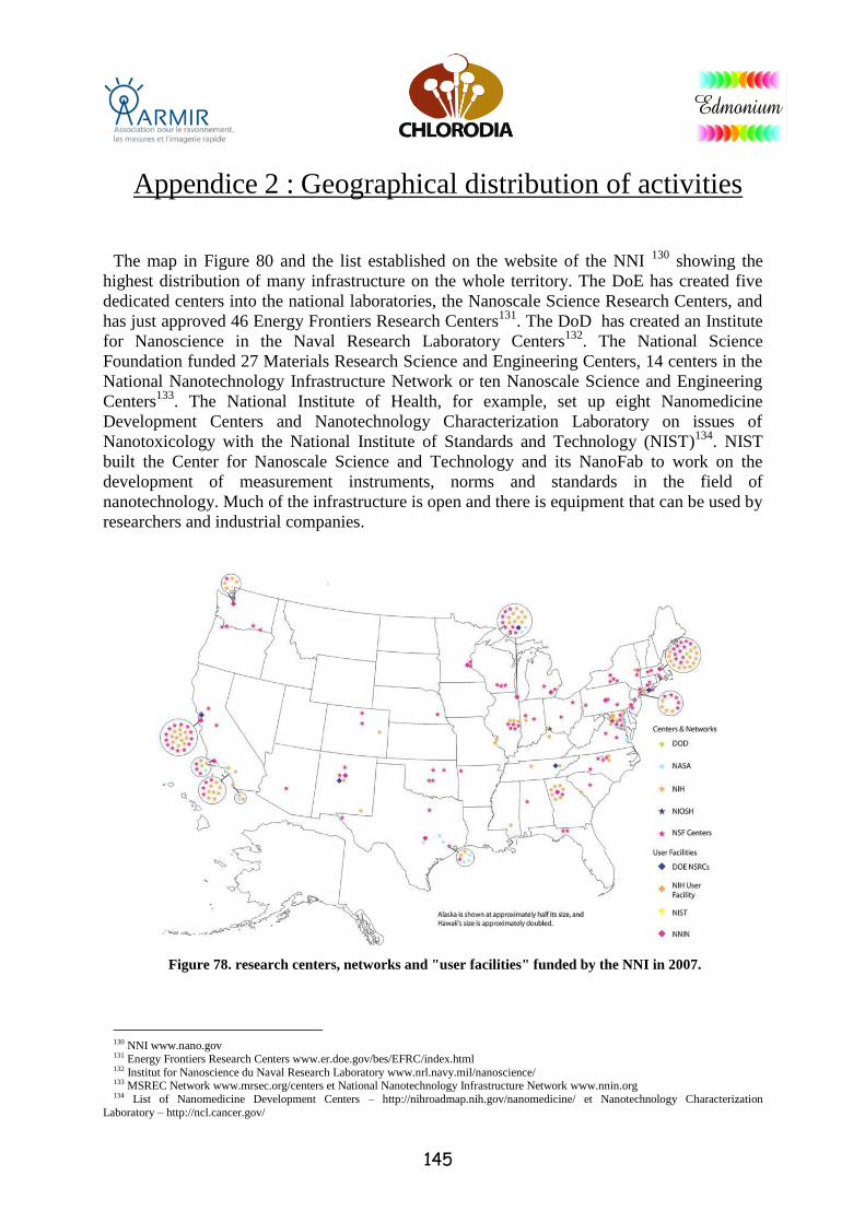
145
Appendice 2 : Geographical distribution of activities
The map in Figure 80 and the list established on the website of the NNI
130 showing the
highest distribution of many infrastructure on the whole territory. The DoE has created five
dedicated centers into the national laboratories, the Nanoscale Science Research Centers, and
has just approved 46 Energy Frontiers Research Centers131
. The DoD has created an Institute
for Nanoscience in the Naval Research Laboratory Centers132
. The National Science
Foundation funded 27 Materials Research Science and Engineering Centers, 14 centers in the
National Nanotechnology Infrastructure Network or ten Nanoscale Science and Engineering
Centers133
. The National Institute of Health, for example, set up eight Nanomedicine
Development Centers and Nanotechnology Characterization Laboratory on issues of
Nanotoxicology with the National Institute of Standards and Technology (NIST)134
. NIST
built the Center for Nanoscale Science and Technology and its NanoFab to work on the
development of measurement instruments, norms and standards in the field of
nanotechnology. Much of the infrastructure is open and there is equipment that can be used by
researchers and industrial companies.
Figure 78. research centers, networks and "user facilities" funded by the NNI in 2007.
130 NNI www.nano.gov 131 Energy Frontiers Research Centers www.er.doe.gov/bes/EFRC/index.html 132 Institut for Nanoscience du Naval Research Laboratory www.nrl.navy.mil/nanoscience/ 133 MSREC Network www.mrsec.org/centers et National Nanotechnology Infrastructure Network www.nnin.org 134 List of Nanomedicine Development Centers – http://nihroadmap.nih.gov/nanomedicine/ et Nanotechnology Characterization
Laboratory – http://ncl.cancer.gov/
146
The NNI has also helped to set up a wide variety of networks to transmit important
information: the InterNano Forum National Nanomanufacturing Network that allows
researchers to exchange information regarding the manufacturing of nanomaterials, the
nanoHUB funded by NSF which includes online simulation tools accessible to the whole
community135
. The NIH has set up a network around the efforts on the treatment of cancer, the
National Cancer Institute Alliance for Nanotechnology in Cancer. Regarding health issues,
safety and environment, the International Council on Nanotechnology maintains on its website a
number of published articles database136.
Finally, on educational issues, it is possible to cite the
Nanotechnology Center for Learning and Teaching (NCLT), useful to all levels of education to
promote and publicize nanotechnology137.
The goal for the next 10 years is to maintain the
infrastructure and capitalize on their potential. The challenge of standards recalled that the
regulation can become a barrier to open markets, and the US will be involved on the standards
that open the way for innovative products and new markets.
135 Internano www.internano.org et Le nanoHUB – http://nanohub.org/ 136 National Cancer Institute Alliance for Nanotechnology in Cancer – http://nano.cancer.gov/ and ICON – http://icon.rice.edu/ 137 NCLT Community – http://community.nsee.us/
147
Appendice 3 : Investisors List
In principle, there are three types of investors:
1. Those who focus on the end market rather than the underlying technology/science.
2. Those who focus on technology/science rather than on the market.
3. Those with vision assessment.
The pre-listed companies investors can be divided according to the stage of evolution of the
company, ie starting from the beginning, middle or end. Currently, conditions in Europe are
difficult to obtain investments in entities in start-up stage.
Applied Ventures 3050 Bowers Ave., P.O. Box 58039, Santa Clara
Venture capital funds from Applied Materials, Inc. a global leader in the field of
nanofabrication technology solutions for the electronics industry. Its portfolio includes:
ActaCell Inc. - next generation technology for lithium-ion batteries, Infinite Power Solutions
Inc - ultra-thin, flexible, rechargeable micro-batteries lithium, Innolume - quantum dot lasers
manufacturer of semiconductors, Nanomix - nanoelectronic detection company, Tera-barrier
Films - high performance flexible barrier film.
Band of Angels
The earliest start-up funding agency. Its portfolio includes Espin Technologies Inc., founded
with the mission to develop the technology to produce nanofibers and commercially based
products nanofibers.
Draper Fisher Jurvetson
DFJ achieve its mission through its DFJ Global Network of funds associated with operations
in the US, China, India, Korea, Vietnam, Russia, Europe, Israel, Brazil and Japan. Over the
past 25 years, DFJ and its partners have supported more than 600 companies, and have led the
way in emerging technology markets including the Internet, mobile communications, clean
energy and health care. DFJ has been proud to support the achievements of the industry,
including Baidu, Skype, Overture, Hotmail, Parametric Technologies, Focus Media, AdMob,
Mobile365, EnerNOC, Tesla, SolarCity, BrightSource Energy, athenahealth, Epocrates,
SpaceX and Synthetic Genomics.
Harris & Harris Group 1450 Broadway, 24th Floor, New York
It first became interested in nanotechnology in 1994 with an investment in Nanophase, who
went public with the result in 1997. In early 2002, this group was convinced that
nanotechnology had matured enough to deliver business flow robust for the indefinite future,
began to focus exclusively on nanotechnology and microsystems. Its portfolio includes: ABS
Materials Inc., Cambrios Technology Corp., Contour Energy Systems, Inc. Innovalight,
Kovio Inc. Molecular Imprints Inc., Nanosys Inc., Nantero Inc.
148
Hatteras Venture Partners
Hatteras Venture Partners is a venture capital firm based in Research Triangle Park, NC,
with a focus on biopharmaceuticals, medical devices, diagnostics, and opportunities related to
human medicine including nano. Founded in 2000. With four funds, the company has more
than $ 200 million under management.
Intel Capital 2200 Mission College Blvd. Santa Clara
Since 1991, Intel Capital has invested more than $ 9.8 billion in over 1,100 companies in 48
countries. Its portfolio includes: FulcrumMicrosystems, Inc. Nanosys, Nexplanar Corp,
Xradia, Energetiq Technology Inc.
Livingston Securities, LLC Livingston Securities LLC, 825 Third Avenue, Second Floor,
New York
Investment bank focused on nanotechnology, also provides access to OPI for companies in
this space. They put several conferences throughout the year ranging from health to energy.
New Atlantic Ventures (NAV)
Made early investments in companies targeting high growth emerging mass markets. Its
portfolio includes: Nantero, proprietary technology to create logic circuits on computer chips
based on carbon nanotubes to "Flash" memory.
149
Annexe 5 : United Kingdom
Appendice 1 : Authorities involved in
Nanotechnologies in the UK
Several structures have been established in the UK in the field of nanotechnology :
The Council for Science and Technology (CST) is the highest advisory committee of the
British government for Scientific and Technological Policy. Its mission is to advise the Prime
Minister and the First Ministers of Wales and Scotland on interdepartmental scientific and
technological issues. CST organizes its activities around five broad themes (research, science
and society, education, science and technology innovation and government) as part of a
medium to long term approach. It is composed of senior representatives of the British
scientific and technological world (often members of learned societies, including the Royal
Society and the Royal Academy of Engineering) and is currently under the joint chairmanship
of the Scientific Adviser to the Prime Minister, Sir David King, and Professor Janet Finch.
To assess the government's actions on nanoscience and nanotechnology, CST set up a
subgroup composed of five of its members, a representative of the Royal Society, a
representative of the Royal Academy of Engineering and a co-opted professor of sociology by
the subgroup138
.
The government's strategy on nanotechnologies is determined by the Ministerial Group on
Nanotechnologies, established in 2007 and including representatives from Defra, the
Ministries of Health (DH), and Employment and Pensions (DWP).
The Nanotechnology Research Co-ordination Group (NRC) was established to
coordinate public funding research in the area of the potential risks of products and
applications of nanotechnology. It is also responsible to establish links in Europe and abroad
to promote dialogue and facilitate information exchanges.
Defra chairs the NRCG. Its members include ministries, regulatory agencies and research
councils.
Nanotechnology Issues Dialogue Group (NIDG), chaired by the Office of Science and
Innovation (OSI), is open to the participation of all ministries and agencies involved in the
British government's program for nanotechnology. It meets four times a year to:
- Coordinating government activities undertaken in response to the report of the
Royal Society and the Royal Academy of Engineering.
138
René David; Nanosciences et nanotechnologies : bilan d'étape des actions du gouvernement britannique, ,
French Embassy to UK, Service of Science and Technology, April 2007.

150
- Provide a platform for monitoring progress and commitments made by the
government and to inform the CST.
- Ensure that the NRCG work fits into the rest of the government's work program.
Nanotechnology Industries Association (NIA) brings together a network of companies
active in nanotechnology. The association was created in 2005 to promote the responsible use
of nanotechnology and to raise awareness in their potential and their possible applications.
The NIA is coordinating the drafting of press releases and documents outlining its positions in
areas relevant to its members.
Nanotechnology Engagement Group (NEG) was established to stimulate new ways of
thinking and methods implemented to involve the general public in nanotechnology. It is
based on existing projects to enact recommendations for future research and practice in this
area. The NEG is funded by the OSI as part of its program Sciencewise.
TSB is responsible for the promotion, support and investment in technological research,
development and commercialization, and provides a translation mechanism of basic research
into new products and services. One way for the TSB to promote innovation in this area is the
Nanotechnology Knowledge Transfer Network (nanoKTN, Nanotechnology Knowledge
Transfer Network), between industry and academia.
151
Appendice 2 : Investisor List Aldermore
Suppliers of specialized lending services to small and medium-sized enterprises in the UK.
He recently provided £ 1.2m installation finances PDA International, one of the areas of
interest is a new material that he developed with an expert in tissue York through
nanotechnology
Amadeus Cambridge Office Mount Pleasant House, 2 Mount Pleasant, Cambridge
Amadeus Capital Partners Limited has over £ 470m under management. This company has
active investments in around 40 companies at any time, across Europe and selectively in Israel
- Invested in Plastic Logic, DocumentPower, Power ID
Carbon Trust Investments Limited
Venture capital investments and seed stage to accelerate the commercialization of clean
energy companies in the UK - Since 2001, they have invested in 25 companies in the UK
cleantech, which raised nearly £ 160 million in venture capital, many in the field of fuel cells
and innovation that could benefit from nanotechnology.
Catapult Venture Managers
Specializes in providing Equity Capital between £ 200k and £ 2M, have invested in over 50
companies - Portfolio includes Pharmaceuticals critical (£ 939,000), the Promethean particles
(undisclosed amount), Diagnostics Ltd Michelson (£ 676,000), Nanotherics (£ 600,000)
Energy Ventures
Independent venture capital dedicated to the upside in the oil field and new gas technologies
- Portfolio includes: Oxane Materials Incfabrique ceramic nano-structured PWA with nano-
glass propriétairesréactive
First Capital Corporation Ltd Elsinore House, 77 Fulham Palace Road, London
First Capital is a European investment bank specializing in assisting companies to
technology so that they run successfully in strategic transactions - Oxonica managed to raise £
4.2mn in a Series A financing round. The union includes a strategic investor, US fund of
venture capital and several British funds.
IP Group plc 24 Cornhill, London
The IP Group's business heart is creating value for its shareholders and partners through the
commercialization of intellectual property - in partnership with a number of academic
institutions in the UK - Corporate Portfolio includes: Chamelic, Ilika, Oxford Nanopore
technologies, Oxford Advanced Surfaces, Nanotecture Group Plc, Surrey nanosystems Ltd,
Stratophase.
London Business Angels (LBA)
Experienced investors who finance innovative enterprises and fast growing - portfolio
includes a £ 250k in the first round in the Electrospinning Company Diagnostics Ltd
Michelson developer and tomography manufacturer optical coherence (OCT) has raised
approximately £ 750k, La company Bac2 own materials and fuel cell components has risen
about £ 3 million.
152
MTI Partners
MTI focuses on start-up companies, particularly those associated with universities.
Headquartered in the UK with a US office in Boston investment includes global companies in
the materials technology, ITEC and medical technology - Portfolio includes the production of
graphene, graphene composites, Fluorographene ....
Octopus Ventures
GPs who tend to focuse on exceptional entrepreneurs teams rather than specific sectors.
Looking for capital efficient companies that can grow explosively create, transform or
dominate an industry. Focused on the UK and can invest from £ 250k to £ 5 million, with £
100 million to invest in the next three years- Portfolio includes, Surrey Nanosystems (£
1.75m), Michelson Diagnostics (£ 1.58 m).
Pond Ventures
Based in Silicon Valley, London and Israel is dedicated to building technology in the
worldwide success Storie - Nanotech Semiconductor portfolio includes a British fabless chip
company that was recently acquired by Gennum Corporation in April 2011.
QIB
QIP (UK) is the UK subsidiary of Qatar Islamic Bank. He invested in NanoSolutions IOTA
which develops nano formulation technologies
Seraphim
Venture capital fund that invests between £ 0.5 million and £ 2 million in high growth early
stage UK companies - Portfolio includes: Pyreos with their sensors based on technology
"thin" Sirigen and technology based on a new form of conductive polymers
The World Gold Council
Invested in startups with nano technology in the field of gold. Two investments to date;
Nanostellar (Diesel Oxidation Catalyst) and Oxford PV (potential use of gold nanomaterials
in photovoltaics).
Top Technology Ventures
Top Technology Ventures - UK venture capital firm specializing in equity financing for
young technology companies based on growth stage. Focuses on high-growth technology
companies, with the first investment is generally between £ 400,000 and £ 1.0 million. In June
2004 Technology Ventures is part of the Top IPGroup plc. Portfolio includes: Nanotecture
Limited, Oxford Nanopore Technologies - Developing nanopore technology, a revolutionary
method of molecular detection and analysis with potential applications in DNA sequencing,
diagnostics, drug development and defense. Oxford Catalysts - specialty Catalysts for the
generation of clean fuels, fossil fuels From Both conventional and renewable sources Such As
biomass.
Ventures Albion
This company had invested between £ 1 million to £ 10 million in a wide range of growing
businesses, companies in technology-oriented service companies. Its portfolio includes:
MEMStar Oxonica, Oxensis, Perpetuum, Teraview ...
153
Unilever Ventures 1st Floor, 16 Charles II Street, London
Unilever Ventures (UV) is the European venture capital arm of Unilever. We invest in start-
ups that could become strategic for Unilever and can benefit from access to Unilever's assets
and capabilities. UV concentrates its investments in: health and vitality. Personal care, digital
marketing, new foods. UV invested in IOTA NanoSolutions which develops nano formulation
technologies.
Wellcome Trust Wellcome Trust, Gibbs Buildingn, 215 Euston Road, London
This fund bridges the gap between basic research and commercial application by funding
applied research and development projects to a stage where they are attractive to a lender.
essential criterion is that the project meets a medical need or vacant is a tool for research and
development of health care. It also offer a variety of other funding schemes.
154
Annexe 6 : Russia
Appendice 1 : The Research in Russia
1. Presentation
The organization of research in the USSR was marked by a separation between R&D
and production, research being conducted in separate structures of production units: institutes
and consulting firms. Research centers can be attached to the military industrial complex, or
to an Academy of Sciences, or finally to a ministry branch partitioned each other. Production
plants had no real R&D internal structures, except for some offices and control procedures.
Since 1992, the Academy of Sciences of the USSR was replaced by the Russian
Academy of Sciences. Despite the name change, it has successfully negotiated its autonomy
and to maintain its control over the distribution of funding to the institutes that were attached
to it, but its budget was drastically decreased.
The previous institutes have been transformed into public or private research
laboratories, or to engineering, consulting and high technology companies. From 1992 to
1995 there has been an evolution of some institutes of the Academy of Sciences to industrial
laboratories, a transformation of institutes into enterprises or branch disappearance, swarming
P.M.E. hightech, created by researchers139
.
In November 1994, the state again reduced the scope of its active support in creating
the Federal Research Centres, status awarded to the best institutes of the Academy of
Sciences. However, only a small fraction of all the institutes of the Academy of Sciences
enjoys this privileged status. These scientific centers of state also saved former military
institutes (twenty sites were affected). Banned from privatization, the RAS institutes had only
alternative to transform themselves into public industrial laboratories
139 When institutes, lack of funding, have been forced to abandon research, many have offered researchers to continue their own projects
alone. This solution, at first, mutually convenient: Researchers ensuring the maintenance of the Institute equipment they needed, hoping to
sell for their own account the results of their own research. Many had indeed received under the socialism some certificates, nominally
assigning authorship of inventions. These certificates have since been transformed into industrial patents, researchers found themselves owners of the technology they had developed, which strongly encouraged to develop their own applications when they no longer paid by the
Institute. This solution to the temporary origin finally gave birth to a myriad of P.M.E. early 1992, more than 300 private companies from
institutes were already registered in Russia.
155
Moreover, Russia has established structures to organize financing in the mode of the
call for proposals: the Russian Foundation for Basic Research was created in 1992 and the
Russian Foundation for the Humanities in 1994.
Other foundations were created to support R&D and innovation:
- for applied research, the Fund for Assistance to Small and Medium Enterprises (FASME)
provides an opportunity for researchers to start or continue their development in the context of
a start-up or SME created even within of their own institute.
- for fundamental research, the Russian Foundation for Basic Research (RFBR) provides
funding for research on selected tenders in order to maintain a good level of research.
Nanotechnology is perceived approximately € 7 million in 2005. It is an independent state
agency created in 1992 under the control of the Ministry of Education and Science (MES).
Scientific research has therefore not, at the beginning of the transition period,
been seen as a potential lever for economic restructuring of the country.
2. The structure of the current research
Russia today is characterized by a huge potential in human resources, but at the same
time by important weaknesses 140
.
The majority of the entities in the Russian research consists of structures for most
inherited from the Soviet era. They numbered 3600 in 2004, which can be classified into
several groups :
- Research institutes of the Russian Academy of Sciences (RAS): the Russian Academy
of Sciences plays a major role because it contributes both to the development of science
policy, in coordination with the Ministry of Education and Science, and the implementation of
this policy, through the guardianship of a network of research institutions (nearly 450
institutes in 2005 and over 100 000 people). The expenses of the ASR totaled in 2005 to € 750
million (representing nearly half the federal budget for basic research).
- Institutes of applied research historically associated to sectoral areas of industrial
activities, which constitute about half the total number of research institutes in Russia.
140A significant portion of the Russian population went up higher education. With over 50% of the younger generation (25-34 years) in
reaching higher education, Russia has the most graduates in OECD countries sciences. Despite the workforce downsizing, Russia can count
on a team of R&D excellence especially in the sciences, inherited from the Soviet Union.
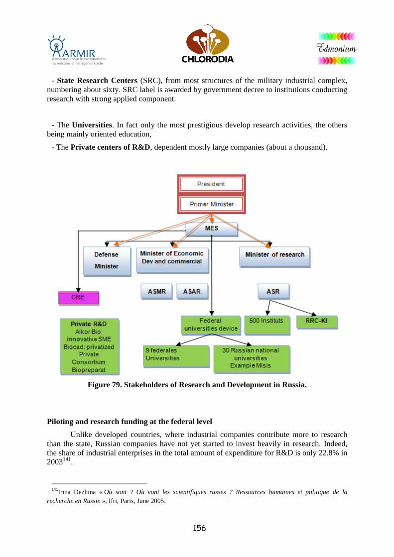
156
- State Research Centers (SRC), from most structures of the military industrial complex,
numbering about sixty. SRC label is awarded by government decree to institutions conducting
research with strong applied component.
- The Universities. In fact only the most prestigious develop research activities, the others
being mainly oriented education,
- The Private centers of R&D, dependent mostly large companies (about a thousand).
Figure 79. Stakeholders of Research and Development in Russia.
Piloting and research funding at the federal level
Unlike developed countries, where industrial companies contribute more to research
than the state, Russian companies have not yet started to invest heavily in research. Indeed,
the share of industrial enterprises in the total amount of expenditure for R&D is only 22.8% in
2003141
.
141
Irina Dezhina « Où sont ? Où vont les scientifiques russes ? Ressources humaines et politique de la
recherche en Russie », Ifri, Paris, June 2005.
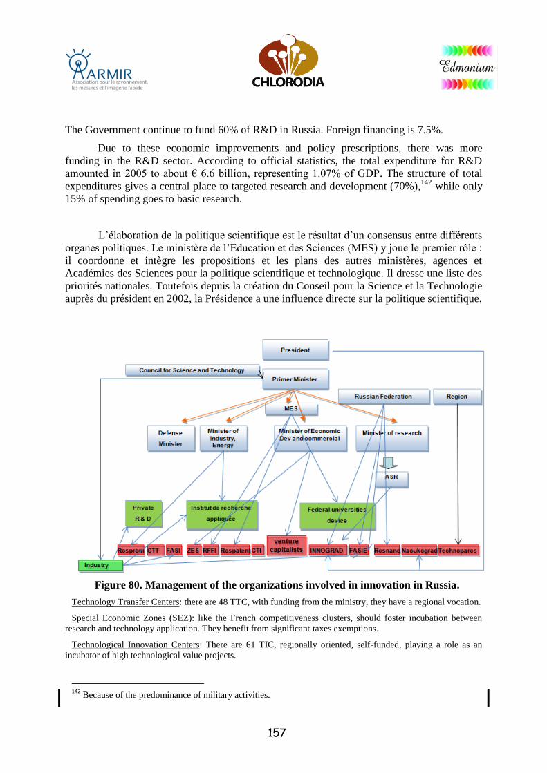
157
The Government continue to fund 60% of R&D in Russia. Foreign financing is 7.5%.
Due to these economic improvements and policy prescriptions, there was more
funding in the R&D sector. According to official statistics, the total expenditure for R&D
amounted in 2005 to about € 6.6 billion, representing 1.07% of GDP. The structure of total
expenditures gives a central place to targeted research and development (70%),142
while only
15% of spending goes to basic research.
L’élaboration de la politique scientifique est le résultat d’un consensus entre différents
organes politiques. Le ministère de l’Education et des Sciences (MES) y joue le premier rôle :
il coordonne et intègre les propositions et les plans des autres ministères, agences et
Académies des Sciences pour la politique scientifique et technologique. Il dresse une liste des
priorités nationales. Toutefois depuis la création du Conseil pour la Science et la Technologie
auprès du président en 2002, la Présidence a une influence directe sur la politique scientifique.
Figure 80. Management of the organizations involved in innovation in Russia.
Technology Transfer Centers: there are 48 TTC, with funding from the ministry, they have a regional vocation.
Special Economic Zones (SEZ): like the French competitiveness clusters, should foster incubation between
research and technology application. They benefit from significant taxes exemptions.
Technological Innovation Centers: There are 61 TIC, regionally oriented, self-funded, playing a role as an
incubator of high technological value projects.
142
Because of the predominance of military activities.
158
Head of State: Since 1991, the President is the key stakeholder in the Russian political system. In particular it
can dissolve the Duma.
Head of Government: Prime Minister. Executive power is exercised by the head of government. The legislative
power is vested in both the government and the two chambers of the Federal Assembly of the Russian
Federation.
Lower House: The Duma, has a leading role in the development of legislation. Upper House: Council of the
Federation, much lower than the Duma.
Russia's venture capital: created in 2006 to deal with weak private venture capital. It had received from the
Ministry of Economic Development a federal allocation of € 420 million and continues to act as a fund of funds.
Council for Science and Technology : Created in 2002 to the President of Russia. The Presidency thus has a
direct influence on science policy.
FASI : Federal Agency for Science and Innovation. It manages several federal programs relevant targeted
Russia for R&D.
Russian Federation: develop innovative SMEs thanks to income from fossil resources.
INNOGRAD at Skolkovo (Moscow): Research center for development and commercialization of new
technologies (energy, information technologies, telecommunications, biomedical, nuclear). Created by the
Academy of Sciences, State Corporation Bank for Development and Foreign Economic Affairs
(Vnesheconombank), Rosnanotec, Bauman Moscow State Technical University, Russian Venture Company and
the FASME
Institutes of applied research: 3566 organizations identified in 2005.
Ministry of Education and Science (MES): established in March 2004, co-ordinate and integrate the proposals
and plans of other ministries, agencies and academies of sciences for science and technology policy.
Naukograd: Physical infrastructure: scientific cities, technoparks, transfer centers and special economic zones.
Rosnauka : Federal Agency for Science and Innovation. It funds research applied call for projects each year:
development of scientific knowledge, technology development, technology commercialization. With a budget of
more de1,15 billion in 2006, RosNauka has funded 2700 projects, including 134 international dimension in
cooperation with 25 countries. Rosnauka Under his tutelage the Russian Fund for Technological Development
Rosprom : Rosprom, born in February 2004 by decree of President Putin, is formed from the merger of several
agencies responsible for armament and Rosavaikosmos Space Agency. Rosprom must finance technologically
innovative industrial projects for 156 million euros between 2007 and 2012.
Technoparks: created in the late 1980s, they are the first element of a policy of infrastructure creation to foster
innovation and technology transfer. They consist of a set of SMEs.
Current policy orientation
Political power took control in 2001 on the foundations requiring them to declare themselves
"governmental organizations" and by assuming ownership rights to the technologies
developed.
In addition, since 2000, things have accelerated and the government has given high priority to
defense and military research by an incentive policy: there was creation of scientific studies,
higher wages proposal for researchers and teachers, etc.
159
3. Conclusion
Aware of the difficulties of Russia to maintain its place in the competitive context of
research and high technologies worldwide, the authorities since the early 2000s (in
continuity with the first efforts initiated towards 1990) undertook a series of reforms
background for boosting basic research and establish a system of innovation and
technology transfer that is both effective and has engaged on the economic realities of the
country. This policy includes a multitude of areas: legal, tax, regulatory, legislative, financial,
help and support from the state, etc.
160
Appendice 2 : Institutes of excellence in
nanotechnology
1. Ioffe Physical-Technical Institute, Russian Academy of Sciences (RAS),
Saint Petersburg
Description
Despite its large size, the activities of this institute are always at the forefront of science and
he managed to turn his technology with many applications in electronics, nano-electronic,
opto-electronic, spintronics, imaging, sensors, etc. It is also a breeding ground for creation of
innovative SMEs.
Specialized topics
Heterostructures, especially in the III-V systems (Nitrides of Ga, Al, In), thin film growth by
epitaxy, optoelectronics, crystalline and amorphous semiconductors, dielectrics, electronics
and nano-electronics, spectroscopy...
2. Chernogolovka Institute of Solid State Physics (RAS), Moscow Region
Description
Founded in the early 60s, the institute is still one of the top performers in its field, especially
at the basic level. An application and development sector is developing dynamically,
especially in the field of materials.
This institute has many links with the outside world, especially with the Landau Institute
theorists. Internationally, it has numerous collaborations, particularly with several French
laboratories for many years (Paris, Orsay and Grenoble).
Specialized topics
Superconductivity, quantum transport, giant magnetic susceptibilities.
Crystal growth of technological crystals, nanostructured materials, nanotubes, quasicrystals,
quantum crystals, semiconductors, ceramics, composites, refractories, etc...
Surfaces, interfaces, physical defects, phase transformations.
Optical, electrical, magnetic, mechanical properties.Spectroscopy and microscopy.
3. Institute of Semiconductor Physics (RAS), Novosibirsk
Description
Founded in 1964, the institute is the best in the field of semiconductors, both in terms of
basic research and applications.
Specialized topics
Growth and structure of semiconductor materials, micro-photoelectron, physics and
technology of semiconductor low-dimensional (micro and nanostructures), quantum
electronics, structures of thin films for microelectronics and photoelectron, physical and
161
engineering of semiconductor structures, R&D development of monocrystalline silicon and
silicon structures. Atomic force microscopy, nanolithography, LIGA.
4. Institute of Microstructure Physics (RAS), Nizhny Novgorod
Description
Although founded only in 1993, IMP is a major nanotechnology centres of excellence
through fundamental research in physics of surfaces and interfaces, semiconductors, high
temperature superconductivity, optics X-rays. His instrumental park, well managed by a
dynamic team (not bloated), allows it to attract good young researchers from the neighbouring
University.
Specialized topics
Physics and technology of metal structures, semiconductors, superconductivity,
heterostructures and nano-systems.
Embodiments of semiconductor sources for terahertz generation frequency and the
components for optoelectronics (photo-luminescence, light emitting diodes).
Scanning microscopy, atomic force tunneling, SNOM, High Resolution Spectroscopy,
MOCVD, MBE, laser ablation, RIE, many systems characterization and tests (X-ray, AES,
SIMS, SEM), Cleanroom Class 1000 and 100.
5. Prokhorov General Physics Institute (RAS), Moscow
Description
Created in 1983 by Academician A.M. Prokhorov (Nobel Prize in 1964 and inventor of
lasers) from the "A" division (plasma physics laboratories) of the Lebedev Institute (created it
in 1934).
Specialized topics
In FORC: Raman fiber lasers and doped, electrostriction effect, photoréfaction effect in
doped fibers, losses mechanisms in fibers doped with germanium and phosphorus, sensors,
fiber to the nuclear industry, research new doping, non-linear crystals, fibers covered with a
metal surface (copper, nickel, etc.). Very good collaboration with French teams (on fiber
lasers with Limoges, nanotubes with ONERA-CNRS, metal surfaces with Nancy).
Nanotechnology: Production and characterization of carbon nanotubes by various methods,
and then processing into film having simple and many applications, heterostructures,
developed on a nanostructured noble metal substrates by reaction with a halogen gas.
6. NikolaevInstitute of Inorganic Chemistry (ASR), Novosibirsk
Description
Created in 1957, this laboratory is one of the first institutions of the new Siberian Branch of
the Russian Academy of Sciences.
Specialized topics
Synthesis (and characterization) of the crystals of all kinds: BGO crystals (10 to 20 Kg)
single crystals doped with rare earths.
162
Nanostructured transparent ceramics, colored, transparent to IR, systems Si (or B) NxCx: H
variable composition. Preparation of metals (particularly rare earth) by reduction of the
corresponding oxide with lithium hydride (LiH).lanthanide borides synthesis (LnB6) almost
as hard as diamond. Super magnets realizable by powder metallurgy.
Polymer chains for micro and nano-materials for storage and transportation of gaseous
hydrocarbons.
Low temperature synthesis of nanocrystalline CdS films, Cdx Zn1-x Cu 2 S and PbS using
dithiocarbonates as single source precursors.
Synthesis by arc discharge andCVD of the carbon nanotubes, possibility of doping, electron
structure (metal or semiconductor), chemistry, properties. Optimization of carbon nanotubes
is sought to achieve nano-X-ray sources and the study of the magnetic properties of Co-Fe
aggregates (collaboration with École Polytechnique: Alexandre Sharaya, Hubert Pascard and
Olivier Klein). Superconductivity.
7. ShubnikovInstitute of Crystallography (RAS)
Description
The Institute was founded in 1943 by the eminent physicist Aleksey V. Shubnikov (1887-
1970) under the auspices of the USSR Academy of Sciences.
This great Institute, dedicated to the Crystallography, is unique. On the multidisciplinary
nature, it is born of geological and mineralogical studies by integrating the chemical aspects,
then evolved towards more fundamental investigations of the crystal (structure, properties,
etc...), with the powerful methods of physics, especially X-ray. It also developed many
synthetic crystal growth processes of different kinds and sizes giving it the status of a national
provider of quality crystals, not only in Russia but also in the global market (Investment 2005:
$ 40 million).
Today, thanks to its multidisciplinary tradition, the Institute has quickly turned to modern
subjects: growing special crystals off gravity (in orbit), LCD (optoelectronic devices), growth
of piezoelectric crystals (mobile phones) or biological and especially nanotechnology. In this
area, the Institute plays a leading role and national coordinator: It was named "national
contact point" for the participation of Russian teams in the programs of the 6th European
Framework Programme.
Specialized topics
Crystal growth and associated technologies (characterization by X-rays, for Synchrotron
Radiation, spectroscopy, microscopy, mechanical, optical, electrical, etc ..), thin film, nano
centers of manufacturing, organic crystals, membranes, nano-biotechnology, ultrafiltration,
liquid crystal, crystal technology (ferroelectric, piezoelectric, magnetic, semiconductor,
quartz, sapphire, oxides, etc...)
8. Institute of Structural Macrokinetics (ISMAN) (ASR), Chernogolovka
Description
Founded in the 70s on the basis of a discovery of his Director, Academician Alexander
Merzhanov, this institute founder of a new branch of chemistry of materials, specializes in the
synthesis of new materials by reactions "SHS" (Self Propagated High Temperature reactions).
163
Specialized topics
Synthetic materials (where most of the elements of the Mendeleev classification were used
successfully), protective coatings, anti-corrosion, ultra-hard materials, thermal shock resistant,
abrasive powders, filtration materials, etc.). Manufacture of ceramic SHS by high pressure
gas, developing new alloys mechanically activated SHS, formationof nano-layer and
multilayer by the SHS process.
9. Boreskov Chemistry Institute of Catalysis (ASR), Novosibirsk
Description
Created in 1958, this is the largest institute of chemistry is Russia. Living largely from
revenues it collects from foreign companies exploiting their patents, the institute has means
for moving from laboratory scale to industrial scale pilot (performance equipment: XPS,
ESCA ...). About a third of its budget comes from contracts, especially with Chinese and
South Korean companies.
Specialized topics
Manufacture of photocatalytic TiO2 (modified Pt powders), fibrous carbon (nanofibers and
nanotubes at 2.5 kg / day), SiC nano-fibers coated with amorphous carbon, nano-diamond for
polishing, carbon (graphite ) for porous filtration, meso-porous materials based on silica,
aerogels SiO2-NiO, etc. Specializing in carbon nanotubes (CNTs), dediamètre nanometer (5
nm), researchers have numerous collaborations ("onion-like carbon").
They also study the manufacturing methods of nano tips for scanning tunneling
microscopes.
Development of new catalysts (Fe-Mn for the synthesis of SiC whiskers...).
10. Chemistry Institute of Solid and Mechanical Chemistry (ASR),
Novosibirsk
Description
Created in 1944 (as "Chemical Metallurgical Institute"). The Institute is organized into three
main areas of investigations, affecting the chemistry of the solid state, the design of new
materials, mechanical and chemical activation chemistry, electro-chemistry, new materials
and bases new technologies.
Specialized topics
Very interesting fundamental work to understand the phenomena occurring during the
synthesis reactions by mechanical-chemistry of nanostructured oxides such Al203 and ZrO2.
Study of the influence of mechanical activation on agglomeration of ceramic oxide powders
in nanometric grains: 20-25 nm (less than 0.5% Fe) and 40-45 nm (less than 0.02% Fe).
Fundamental study of SHS process with investigations on the neighbouring Synchrotron, to
access measures diffractometric fast enough to follow the kinetics of reactions. SHS process,
coupled with mechanical activation (high energy milling) is used for synthesizing
nanopowders at low cost.
Sintering of nanopowders leading to well densified ceramic in which the nano-structuring is
preserved by SPS technology (Spark Plasma Sintering) with Korean.
164
Development of nanostructured deposits TiB2 / Cu electrical discharge (electric arc) for
electrode.
Fluent deposition of protective coatings (Al203, ZrO2) on nano-grains of C or SiC.
Institute turned to the Far East (Japan, Korea, China) for lack of collaborations with Western
laboratories.
11. Laser Physics Institute (ASR), Novosibirsk
Description
Founded in 1991, the Institute remains one of the best in the field of basic research in lasers
and has recently developed a number of applications, particularly in medicine.
Specialized topics
High resolution spectroscopy, frequency stabilization (He-Ne/CHn), femtosecond optical
clock system and frequency synthesizer, cooling of atoms, etc.
On the sidelines with these fundamental studies, the Institute develops many elements of
optical frequency standards, femtosecond synthesizers, lasers for medicine, biology and
ecology, tunable single-frequency lasers, optical clocks femtosecond fluorescence
spectrometers, laser instruments to measure small displacements, excimer lasers, etc.
This Institute is being relocation to Moscow and St. Petersburg, the future direction of his
research are not clearly visible despite strong ties with the University of Paris-Nord
Villetaneuse (it is part of a Franco-Russian GDRE) and other strong international
partnerships, mainly with Germany, Britain, Japan and Korea.
12. Institute of Strength Physics and Materials Science (ASR), Tomsk
Description
Founded in 1991, the Institute is probably the best in the field of mechanics of materials,
both in basic research and for numerous applications in the synthesis of new materials with
high mechanical and functional characteristics. Very active, with close collaborations with
other Tomsk centers, ISMAN of Chernogolovka and Solid State Chemistry Institute of
Novosibirsk, the Institute attracts many quality young researchers.
Specialized topics
Fundamental work on nanomaterials: thermodynamic and mechanical calculations on the
grain boundaries in nanomaterials compared with the same materials but with micrometric
grains. Experimentation and modeling.
Development of nanostructured bulk materials by PSD (Severe Plastic Deformation).
Titanium Application: pure titanium obtained by PSD can be used, instead of its alloys for
prostheses (no toxic alloying elements).
Nanostructured materials: surface treatment, production of superhard coatings (Ni3Al) for
cutting tools and machine parts (microhardness of 35-55 GPa).
Surface treatments on the treads of railway wheels, inner linings of molds.
165
Superhard nanostructured coatings: Altio, ZrTiNC, AlTiON, AlTiNC, TiN, TiC, TiCN,
TiBCN; up to 20 Pa. électroplasma coating solution including light metals (IT, Al) for
reinforcement and protection (Y2O3 Al seems possible).
Synthesismethod of oxide nanopowders by plasma (ZrO2-Y2O3-Al2O3 9 nm, ZrO2, 3%
Y2O3 20 nm) of alumina nano-fibers (applications for ultra-filtration).
Preparation of nano-ceramics (ZrO2 / Al2O3 composite) with a controlled porosity between
10% and 70%.
Preparation of highly dense ceramic for cutting tools.
13. Other centers of interest with activities in Nanotechnology and
Materials
Moscow: Lomonosov University, MISIS University, Mendeleyev University, MIPHY
University, General Physics Institute (RAS) and the Fiber Optics Research Center (FORC)
Region of Moscow: Zelenograd: NT-MDT Company ; Chernogolovka: Institute of Problems
of Physical Chemistry and the Institute of Microelectronics Technology and High Purity
Materials ; Troitsk: Physics Institute of High Pressure, spectroscopy Institute
St. Petersburg: State University of Technology: Inorganic materials, ceramics and glass,
hybrid metal/ceramic, fibrous single crystals. Centre Svetlana-Optoelectronics:
electroluminescent diodes
Ekaterinburg: Institute of Metals and Institute of Electrophysics
Nizhny Novgorod: University "Lobachevsky": semiconductor nanostructures, epitaxy of
GeSI islands on single crystal silicon, nano-Si crystals embedded in a matrix of amorphous
silica on silicon (luminescence).
166
Appendice 3: Valuation of Russian Research by
Rosnanotech Until recently, Rosnanotech (Russian Corporation of Nanotechnology: CENT or
Russnanotekh, July 2007) communicated little about its activities. It was during the
International Economic Forum in Saint Petersburg in June 2011, Anatoly Chubais, Chief
Executive General and executive board chairman, spoke to bring more information:
It is a company that invests in innovative nanotechnology, it also helps companies when
marketing.
Rosnanotech projects by category:
• Nanomaterials: 44%
• Technology of efficient energy: 15%
• Pharmaceutical products: 17%
• Nano-coatings: 10%
• Optical and electronic: 10%
• Other: 4%
Rosnanotech has an important role in various stages of R & D. Particularly in the private
sector, Russian or foreign, if part of the production is done in Russian. It is also involved in
the public domain through the training of specialists, partnerships with private investors, the
financing of innovative projects that may lead to startups. As venture capital, it promotes the
transfer of technology. In the industrialization phase, it can finance infrastructure, certification
and risk assessment, but it rarely provides more than half the share of investment. It accepts
an average of 1 file out of 20 candidates.
Some numbers:
• Applications for funding: 1,967
• Applications approved: 113
• Total budget: 381.6 billion rubles
• Number of applications submitted by the companies: 30
• Number of regions involved in the project Rosnanotech: 30
[NIKITA DULNEV, Rosnanotech’s big nanotechnology secrets revealed, Russian Beyond
the headlines, 3 August 2011]
Rosnanotech was founded in March 2011 as a corporation, opened by the reorganization of
state corporation Russian Corporation of Nanotechnologies. The Government of the Russian
Federation owns 100 percent of shares of Rosnanotech. Anatoly Chubais is the executive
director of Rosnanotech.

167
[Rosnanotech and NEARMEDIC PLUS to Create New Nanomedicine Production Facility,
Rosnanotech, 17 octobre 2011]
“Russian Corporation of Nanotechnologies” activity until the year 2015
[Business strategy of State Corporation “Russian Corporation of Nanotechnologies” until
the year 2020, Rosnanotech, mai 2008]
Team : Leonid Melamed 1° General Director, M. Anatoly Tchoubais143
(sept 2008) 2°DG
M. Malyshev Deputy Director
M. Mostinsky/S. Motsinskiy International relations Director
Rosnanotechannounces the incorporation of investment management
companyRosnanotechCapital AG, June 30, 2010
Rosnanotechannounces the completion of the incorporation and registration procedure for
the investment management company RosnanotechCapital AG. RosnanotechCapital AG will
be involved in attracting global investors for financing promising Russian innovative projects
as well as investing in existing international technologies with the aim of implementing them
in Russia.
143 First Deputy Prime Minister (1992-1996 and 1997-1998) built the privatization program. Appointed in 1998 to head Rao United System
(ues), public monopoly producing 70% of Russia's electricity, he led the reform of the electricity sector, officially ended with the
disappearance of Rao ues on 1 July 2008. Currently responsible development of nano-industries in Russia.
168
RosnanotechCapital AG is registered in Switzerland and will monitor and maintain control
over the establishment and activities of funds invested in specialized innovative technologies.
Andreas Kazutt, a partner in the law firm “Niederer Kraft & Frey”, has been appointed as the
Local Director of RosnanotechCapital AG in Zurich.
Rosnanotechis the exclusive shareholder of RosnanotechCapital AG and for the purpose of
conducting consulting activities in Russia a subsidiary company called RosnanotechCapital
LLC has been incorporated. RosnanotechCapital LLC is headed by Irina Rapoport.
“Our intention is to render integral support to our partners as per issues concerning gaining
access to investments in Russian research activities and challenging projects,” - Irina
Rapoport said. “We are already aware of global players’ interest in different research and
development activities, including such areas as: alternative power-engineering, innovative
materials, biotechnologies and pharmacology. We trust that we’ll be able to considerably
increase the volume of foreign investments in leading Russian research and development
activities as well as make our contribution to world innovative technologies transfer to
Russia.”
Source: Rosnanotech (press release)
RosnanotechSigns Investment Agreement for the SynBio Innovative Pharmaceuticals
Project, 5 août 2011.
Rosnanotech, the Human Stem Cells Institute, Pharmsynthez, Cryonix, FDS Pharma LLP
(United Kingdom), and private investor Dmitry Genkin have signed an investment agreement
for the SynBio project. The project’s purpose is to develop innovative medicines and biobetter
pharmaceuticals. Lipoxen PLC, a British pharmaceuticals developer for leaders in the global
pharmaceuticals industry, and German company SymbioTec GmbH will be the principal
R&D partners for the project.
The partners have established limited liability company SynBio to carry out the project,
which has a total budget of 3.2 billionrubles. Of that sum, Rosnanotechwill co-invest up to
1.3 billion rubles. The other founders will co-invest up to 1.9 billion rubles in the form of
monetary resources, intellectual property rights, and shareholding in their own and subsidiary
companies. The investment period will be four years, and the project is slated to run seven.
The SynBio project will develop and launch nine pharmaceutical products for Russian and
international markets. The medicines are based on three technological platforms:
stem cell technologies for treatment of chronic diffuse liver disease (the Gemacell
platform)
intranuclear human protein histone H1 for treatment of cancers and other diseases (the
Histone platform)
sustained-release drugs using polysialic acid-biobetters for treatment of diabetes mellitus,
Alzheimer’s disease, chronic kidney disease, and other illnesses (the PolyXen® platform).
169
Biobetters resemble biotech pharmaceuticals that already exist in the market, and they differ
in that they surpass the biotech preparations by certain characteristics, such as effectiveness.
All the medicines in the project are currently undergoing pre-clinical tests or clinical trials in
research laboratories in Russia and Europe. All the pharmaceuticals developed within the
project areexpected to be sold in the Russian and international markets. Sales of SynBio’s
drugs in 2015 are forecasted at 700 million rubles.
"Two facilities will be established for commercial production of the innovative medicines,
one each in Leningrad and Moscow oblasts," explained Olga Shpichko,
Rosnanotechmanaging director. "Manufacturing will be set up jointly with our German and
British partners. We regard this as a step toward entering the international pharmaceuticals
market."
Artur Isaev, general director of the Human Stem Cells Institute: "It would be difficult to
over-estimate the importance of today’s events for us and our partners. This is the first time
that a Russian company has initiated a M&A in the biotechnology sector to serve the Russian
and global markets. The project intends to introduce a number of innovative drugs that will
bring real progress in the treatment of socially significant diseases. Our project is an excellent
example of how the government’s program for innovative development of the Russian
pharmaceutical sector can be implemented."
An R&D center for composite materials will be opened atSkolkovo10/26/2011
As part of the 4th International Nanotechnology Forum, the Skolkovo fund and
theComposite Holding Company signed an agreement to organize an R&D center for
carbonfiber based polymer composite materials which will be located at Skolkovo. The
documentwas signed by Viktor Vekselberg, president of the Skolkovo Fund and Leonid
Melamed,president of the Composite Holding Company in the presence of Sergei Kirenko
head ofRosatom State Corporation and Rosnanotechchairman of the board Anatoly Chubais.
The signed agreement established primary target parameters up to 2015 for the
R&Dcomposite materials centerwhich will become part of Skolkovo Innovation Center. The
newcenter will employ 25 people, including 2 foreign specialists.
The total investment planned for the R&D center until 2014 will be around 600
millionrubles, including 300 million that Composite Holding Company plans to attract from
theSkolkovo fund. The annual budget of the R&Dcenter, will be approximately 200
millionrubles starting from 2015.
The Composite research and development center (hereafter Composite RDC) will
conductresearch as part of Skolkovo’s nuclear technology program supported by the
SkolkovoFund. The primary mission of the R&D center is to conduct research aimed at
perfectingcarbon fiber production technologies. This research will be focused on development
of newmethods for production of polyacrylonitrile precursors and carbon fibers, and on
creation ofnew products made of high-test polymer composite materials. The main goal is
tosubstantially raise the quality of Russian-manufactured carbon fiber and provide
lowerprices for such material. Carbon fiber is extremely light, durable, and highly weather-
lightand penetrating radiation resistant. These fibers are used to reinforce composite,
170
insulation,chemo-resistant and other types of materials and as addition to various carbon
plastics.
“In our program of polymer composites usage in the atomic industry products, which
makesprojections up to 2020, we have a separate section dedicated to scientific research in
thisfield. We are prepared to test solutions which will be brought out by this R&D center at
ourproduction facilities, and successful ideas can be applied not only at our own facilities,
butalso in other branches of atomic industry.” Sergey Kirienko said.
Viktor Vekselberg noted: “It is gratifying, that more and more Russian companies
areshowing interest in finding practical forms of cooperation with the Skolkovo fund. We
arealready supporting creation of research structure at Skolkovo for such Russian
companiesas Sberbank, Information Satellite Systems named after academic Reshetnyov, and
Rocketand Space Corporation “Energiya”. Working with the Composite company will make
itpossible to support development of Russian skills and technology in the field of
compositepolymer materials, which, in many ways, is significantly less developed in Russia
than in theleading countries. Scientific research dedicated to perfecting technologies for the
productionof carbon fiber is of extreme importance; after all, this is a unique material, the
material ofthe future. Its characteristics have tremendous potential for use in various branches
ofindustry, which makes it possible to truly consider it as one of the materials of the
21stcentury. This R&D center is created in order to significantly raise the quality of
Russianmanufacturedcarbon fiber, and reach the level of skill and technological development
thatexists in the rest of the world.”“Until quite recently, corporate science in the field of
polymer composite materials basedon carbon fiber in Russia existed on an isolated basis.
Using this composite materials R&Dcenter, we plan to bring pure science, universities and
business together. Our goal is toorganize the process in a way that science will solve problems
important to business.” SaidLeonid Melamed.
Information. The Skolkovo Fund
The development fund for the Skolkovo center for the development and commercialization
of new technologies is a nonprofit organization, created by an initiative of the president of the
Russian Federation, Dmitry Medvedev, in September of 2010. The Fund’s mission is to
mobilize Russia’s resources in the field of modern applied research, the creation of an
encouraging environment for new developments in five significant fields of science and
technology: energy and energy efficiency, space, biomedicine, nuclear and computer
technology. This project involves the creation of the Skolkovo institute of Science and
Technology (SIST), research institutes, a business-incubator, a center for the exchange
oftechnology and commercialization, representative offices of foreign companies and R&D
centers, living facilities and social infrastructure, as well as establishing an effective system
for the distribution of Russia’s investment resources. The activities of the Skolkovo
innovation center are regulated by a special law, which guarantees special economic
conditions to its residents. www.i-gorod.com
The Composite Holding Company was created in order to form a market for composite
materials in Russia in 2009. This vertically integrated holding company includes enterprises
involved in producing highly durable and highly modular carbon fibers (JSC Argon, LLC
Composite-Volokno, LLC ZUKM), fabrics based on those fibers and high quality prepregs

171
(CJSC Prepreg-SKM), which are used in the aviation industry, construction, the automotive
industry, shipbuilding, etc. Among the Holding’s tasks are the creation of highly efficient,
environmentally friendly production of carbon fiber and carbon fiber products on the basis of
innovative technologies for the production of continuous and discrete fibers. The
CompositeHolding Company plans to occupy a leading position in the engineering,
production and sale of next-generation composite materials and satisfy the demands of the
aforementioned industries for domestically made next generation composite materials.
The Rosnanotechforum is a place to discuss and demonstrate innovate technology in
machine building and metal processing, optical electronics and nano-electronics, solar energy
and energy efficiency, medicine and biotechnology, the new branch of industry devoted to
producing nano-patterned materials, and infrastructure projects.
The Forum’s mission is to give participants an opportunity to discuss the primary tendencies
of global scientific and technical development and key trends in the investment process in the
hi-tech sphere, and encourage the practical commercialization of new projects inside Russia:
present concepts to potential investors and partners,
select promising investment opportunities,
find suppliers of innovative products,
create a network for the completion of projects,
establish new contacts on various levels.
The international nanotechnology prize, ROSNANOPRIZE, is proudly awarded at the
Forum. The Forum program includes an award ceremony for recipients of the Russian youth
nanotechnology prize and the winners of the international scientific papers contest for young
scientists working in the field of nanotechnology.
Rosnanotech2010 brought together more than 10 thousand participants from 50 countries.
During the Business and Science and Technology programs of the Forum, more than 400
presenters spoke. These speakers include Nobel Prize winners Academic Zhores Alferov,
Professor Konstantin Novoselov, provost of the Massachusetts Institute of Technology Rafael
Reif, and General Director of Microsoft Steve Ballmer. The plenary session of the Forum was
opened by the president of the Russian Federation, Dmitry Medvedev. Hundreds of Russian
and foreign companies have presented their designs at the Forum’s exhibition. More detailed
information about the Rosnanotech2011 forum is available on the website:
www.rusnanoforum.ru
[An R&D center for composite materials will be opened at Skolkovo, Rosnanotech, 26
octobre 2011]
1 Nanotechnology in the service of medicine, co-investisseur rosnanotech, 19 juillet
2010
Russian nuclear physicists at the “Alpha” Research and Production Facility in Dubna have
developed an advanced apparatus for plasmapheresis. There is no analogous apparatus
elsewhere in the world. According to the developers, the purification of blood using

172
nanotechnology saves the lives of Russians from atherosclerosis and many other serious
illnesses.
There is a need to remove toxins from blood to treat atherosclerosis. The plasmapheresis
removes cholesterol and lipoproteins that forms plaques in the inner lining of the arteries.
Russians use only imported equipment to follow this procedure, and it costs about 1, 000 U.S.
dollars per patient. The development by the scientists in Dubna makes the treatment
accessible for a large number of patients since it is several times cheaper than the foreign
technology.
The Russian scientists suggested using a nano-filter for plasmapheresis. It is made out of a
film similar to one which is used in the food industry. The film is placed in a cyclotron where
it is subjected to the bombardments of argon atoms. Then it is placed in alkaline to create
nano-holes at the places where atoms hit it. In the end, we get a punched film with 200
nanometer diameter holes. In fact, the diameter of a hole is 250 times less than that of a hair.
When blood passes through such a membrane filter, it is separated into parts, erythrocytes
settle on the membrane and plasma, the basic bearer of viruses and antibodies, is removed,
says an expert at the “Alpha” Centre, Yuri Prytkov.
“Plasma passes through the membrane, and blood bodies are separated and return to the
patient,” says Yuri Prytkov. ”The “Alpha” Research and Production Facility has started
producing these apparatuses, which are quite compact. In this case, a centrifuge is not used to
separate blood, and consequently the apparatus can be used also in field conditions. This is
portable equipment and experts can carry it to a patient and do plasmapheresis at his home. It
can be used by the military, rescuers and services for disaster medicine.”
The state-run “Rosnanotech” is the co-investor of the project that has already allocated 1.3
billion rubles or 43 million U.S. dollars to implement it. This sum will be used to build a
facility to start the production of the apparatuses for cascade plamapheresis. According to
estimates, this sum will be paid off in 4-5 years. According to “Rosnanotech” the
development by Dubna scientists is an example that Russia’s scientific potential is being
turned onto the commercial track.
http://english.ruvr.ru/2010/07/19/12759176.html
2 T-Platforms Group Chosen to Manage $6 Million Nanotechnology and
Supercomputing Enablement Program, 31 st 2010
Applicants selected by a RosnanotechExpert Council will receive 75% funding for approved
projects.
T-Platforms Group, a leading provider of HPC systems, software, services and solutions,
was chosen by the Russian Corporation of Nanotechnologies, Rosnanotech, to lead the
program management and execution for a competitive solicitation that will provide
collaborative funding and development support for at least 20 nanotechnology-related
computational tasks and 20 computational tasks from industrial production organizations. The
industrial production tasks will be selected from specific industries targeted by this program

173
to include engineering in areas such as shipbuilding, aerospace, automotive, oil and gas,
chemistry, pharmaceuticals, energy and construction.
As part of this program, worth $6 million over a ten-month period, T-Services, a T-
Platforms Group company acting as program manager, will evaluate applicants based on
criteria such as potential importance, practicality, possible ROI, and applicability to spawning
commercially sound results or products. Organizations will go through a two-stage process,
and those selected for this program by the Expert Council under the leadership of
Rosnanotechwill receive 75% of the funding of the total computational project costs. T-
Platforms, another T-Platforms Group company, will provide T-Services with a dedicated
cluster for this project.
The Nanotechnology and Supercomputing Enablement Program has been designed to create
a supercomputing service infrastructure based on end-to-end guidance, support and
professional services. This is a significant effort on behalf of the Russian government to
establish a robust commercial market for supercomputer simulations – an approach that could
have a significant impact on improved production and productivity for many industrial /
commercial market segments.
“The vision and leadership of Rosnanotechdemonstrates this country’s keen understanding
of the vital importance of supercomputing and the impact scientific and engineering discovery
will have on the future of this planet,” said Vsevolod Opanasenko, CEO of T-Platforms
Group. “We are pleased to have been selected for this very important project and look
forward to our collaboration with Rosnanotechand our other program partners as we strive to
eliminate many of the barriers to widespread HPC adoption.”
T-Services will work in close collaboration with the Joint Supercomputer Center of the
Russian Academy of Science, the Computational Center of Moscow State University (MSU),
Vladimir University, and Tomsk University to provide needed supercomputing resources.
Evgeny Evdokimov, Managing Director of Rosnanotech, said: “This program allocates
funding to help organizations developing products or technologies that are deemed important
for future productivity. Advancing the use of supercomputing for modeling and simulations
has been identified as a vital competitive element to advancing scientific and engineering
discovery, and we are pleased to partner with T-Services on this leading edge program.”
“The Rosnanotechprogram is seeding the scientific discovery efforts within Russia, but
more importantly, it can be seen as a potential forerunner for a new way of funding and
managing large-scale HPC projects,” said Addison Snell, CEO of InterSect360 Research, a
market research and consulting company dedicated to the worldwide HPC industry.
“Rosnanotechrecognizes HPC as the enabling technology for scientific and engineering
progress, and it matches the responsibility of HPC stewardship with the expertise of T-
Platforms. This takes us a step closer to HPC as a service for large-scale deployments, which
could have long-term benefits for scientific and commercial productivity.”
174
About T-Platforms:
Established in 2002, T-Platforms Group is rapidly emerging as one of the leading global
HPC companies, providing comprehensive supercomputing systems, software and services,
with customer installations consistently included on the TOP500 worldwide list of the most
powerful supercomputers.
T-Platforms Group consists of T-Platforms, T-Services, T-Massive Computing, and T-
Design, with locations in Hannover, Moscow, Kiev and Taipei.
About Rosnanotech:
The Russian Corporation of Nanotechnologies (Rosnanotech) was established in 2007 by the
Russian government as a state corporation that co-invests in nanotechnology industry projects
that have high commercial potential or social benefit.
Grand Prix of the Federal Russian Competition “Russian Innovations”, 9 juillet 2010
The Scanning Probe Microscope SOLVER NEXT – the Product of NT-MDT Co. – got the
Grand Prix of the Federal Russian Competition “Russian Innovations”
The Competition “Russian Innovations” is 9 years old. It is held by authoritative Russian
media holding “Expert”. The partners of the event are the main nano-organizations in the
country “Rosnanotech” and “ROSATOM”. The competition is an essential part of Russian
innovation and nanotechnology development program. It plays a very important role in
launching and promoting new high-tech developments in Russia and worldwide. Getting
publicity to nanodevelopers and producers, the event increases investing rate in nano-sector.
Moreover, the competition helps to expertise new tools and ideas and to select only
perspective ones. So, it raises the confidence rate to nano-sector in Russia.
The Scanning Probe Microscope SOLVER NEXT has managed to receive Grand Prix of the
“Russian Innovations-2010”. Its producer NT-MDT Co. names it “the state-of-the-art
company’s development”. This tool offers both atomic force (AFM) and scanning tunnelling
microscopy (STM) under one hood. This enables researchers to gain the fastest time to
results, excellent performance, increased accuracy, high reliability and unprecedented ease-of-
use with no loss in resolution. The flexible, sleek and functional system incorporates smart
software, automated head exchange, and motorized sample positioning under video monitored
control. This allows for high quality images without the need for specially trained operators.
The system has closed-loop sensors to compensate for inherent piezoelectric imperfections
such as scan nonlinearity, creep and hysteresis. With two additional removable heads for
operating in liquid environments and nano-indentation one has the freedom to work with a
variety of samples, measuring modes and conditions. The SOLVER NEXT has an advanced
controller with a vast library of scripts and both Mac® and Windows® compatibilities. The
result is an image-friendly operating system well-suited to large file, 3-dimensional
mathematics and manipulation.
175
So, the tool is designed to meet a researcher’s current and future needs. This innovative
device at the forefront of scientific research opens up new paths of study in different fields of
nanotechnology, providing all user levels with a full range of conventional SPM measuring
techniques (such as topography, phase imaging, nanolithography and more). SOLVER NEXT
provides a robust, diverse, and economic solution for universities, industrial, routine
biological and pharmaceutical labs. It makes AFM and STM accessible to a broader audience,
even offering a special iPhoneTM applet for simple image analysis and image sharing.
Innovation Lift at Work: Rosnanotechto Support Production of Anti-aging
Nanocosmetics28.10.2011
Rosnanotechis joining a project that will produce cosmetics based on double encapsulation
technology. Earlier, the project attracted financing from Russian Venture Company’s Seed
Investment Fund. The project has a total budget of 65 million rubles. Rosnanotechwill receive
an 18% interest in Nanoderm-Profi, the project company.
The project will produce anti-aging cosmetics, skin cleansing agents, and professional
agents for cosmetic salons. The technology underlying production was developed in Ufa,
Republic of Bashkortostan, by Zhespar-Bios and the Ufa Science Centre’s institutes of
Biology and Biochemistry and Genetics, both affiliates of the Russian Academy of Sciences.
The cosmetics are non-toxic and highly effective, thanks to the technology of double
encapsulation. The active ingredient—uronic acid—is embedded in nanoparticles of
cyclodextrin of less than two nanometers. Those particles are, in turn, surrounded by a
spherical capsule of beta-cyclodextrin and plant-based lipids with diameters of
80 nanometers. When the nanostructures are applied to the skin, the external capsule dissolves
and the nanoparticles of cyclodextrin transport the active ingredient through the transdermal
barrier to the skin’s deep layers.
Project company Nanoderm-Profi is already producing and selling the first series of its
nano-cosmetics. Earlier, the agent passed organoleptic, physiochemical, microbiological,
clinical-laboratory, and toxicological testing by Rospotrebnadzor, Russia’s Federal Service
for Supervision of Protection of Consumer Rights and Human Welfare. As this project
develops, Nanoderm-Profi plans to expand its assortment of active components.
“The project to produce anti-aging cosmetic agents won investment from the Seed
Investment Fund of Russian Venture Company at the early stage of development. Today we
have signed documents for a new large round of investment with Rosnanotech. In our view,
this demonstrates two important things,” said Yan Ryazantsev, director of the Department for
Investment and Expertise, Russian Venture Company. “First, that cooperation among Russian
institutions for development is in a healthy spot. And second,that an important element in
technical entrepreneurship—innovation lift—is fulfilling the goal set for it. We are confident
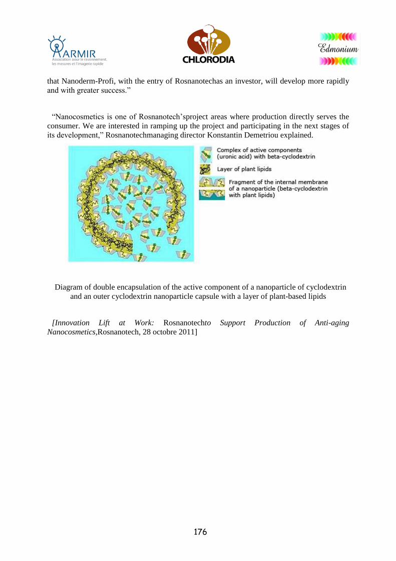
176
that Nanoderm-Profi, with the entry of Rosnanotechas an investor, will develop more rapidly
and with greater success.”
“Nanocosmetics is one of Rosnanotech’sproject areas where production directly serves the
consumer. We are interested in ramping up the project and participating in the next stages of
its development,” Rosnanotechmanaging director Konstantin Demetriou explained.
Diagram of double encapsulation of the active component of a nanoparticle of cyclodextrin
and an outer cyclodextrin nanoparticle capsule with a layer of plant-based lipids
[Innovation Lift at Work: Rosnanotechto Support Production of Anti-aging
Nanocosmetics,Rosnanotech, 28 octobre 2011]

177
Appendice 4 : Russia building its own “Silicon Valley”
23 June 2010
Russian president Dmitry Medvedev flew to California this week to drum up support for
his country’s attempt to build an entrepreneurial enclave just outside Moscow.
He met with California governor Arnold Schwarzenegger on Tuesday, and plans to meet
with the founders of Twitter, as well as Google CEO Eric Schmidt, before meeting US
President Barack Obama in Washington D.C.
Over the past four months, Russia has been building it’s own version of California’s Silicon
Valley, called the Skolkovo ‘innovation city.’
“I want to see how things work on Silicon Valley. We would like to create something
similar in the Russian Federation – adjusted to suit our views, of course,” Medvedev said in a
Wall Street Journal interview.
To reduce its economic dependence on natural resources such as oil and natural gas, Russia
has been pouring its efforts into high tech development. The government created a company
called Rosnanotechto invest in nanotechnology, and has been supporting regional venture
funds to invest in tech companies.
Medvedev also plans to meet with representatives with Cisco Systems, Yuri Milner, CEO
of Russian investment firm Digital Sky Technologies, and Arkady Volozh, CEO of Yandex,
Russia’s largest search engine.
Social Times by Kenneth Musante
178
Appendice 5: very substantial financial resources for
R&D, the Federal Targeted Programs
The federal target program "Research and Development as priority directions of growth of
the Russian scientific and technical complex 2007-2012", based on the order of the
Government of Russia July 6, 2006, is primarily coordinated by the Ministry of Education and
Science. Other concerned government agencies are RosNauka (Federal Agency for Science
and Innovation), RosObrazovanie (Federal Agency for Education) and MGOu (State
University Lomonossov Moscow).
It can be presented following five priority thematic orientations: living systems,
nanomaterials and nanotechnologies, ICT, rational use of natural resources and energy
efficiency.
The program is divided into two stages. Between 2007 and 2009 efforts should focus on
accelerating the commercialization of technologies prioritized by the Russian President, by
attracting additional resources. Between 2010 and 2012, efforts will focus on the development
of structures and mechanisms to support long-term innovation.
Nanotechnologies represent 40% of the planned R & D funding following the Federal
Targeted Programme for 2007-2012, almost € 1.25 billion over 6 years, increasingly (€ 143
million in 2007 and an annual growth of 25 %). In addition, research in the field of
nanotechnology are not conducted only in the context of this federal target program, but in
applications "off budget" for the work done by the institutes of the Academy of Sciences of
State and by higher education institutions, in the quote by funding framework. Thus, within
the Presidium of the Academy, two programs concern nanoscience, materials and on the
electronic equipment.
The program has set a number of priorities for R&D (2007-2012):
- Accelerated development of scientific and technical potential,
- Realization of priority directions through major marketing projects in technology,
- Consolidation and concentration of resources through expansion of public-private
partnership mechanisms, for example by stimulating R&D orders from the private sector,
- Encouraging the inflow of young specialists to the R & D, development of major scientific
schools,
- Development of research activity in universities and graduate schools,
- Support the development of innovative SMEs and their integration into the system of
scientific and technological cooperation,
- Development of a base of competitive scientific organizations conducting basic and
applied research,
- Development of effective infrastructure elements of the innovation system.
These qualitative objectives are accompanied by quantitative targets (over the entire
duration of the program):
179
- Additional production of high-tech products: € 4.3 billion for the commercialization of
technologies developed,
- Export additional high-tech products: 1.1 billion €,
- Attraction of non-budgetary resources: 1.7 billion €,
- Increase in domestic expenditure on R & D, including off-budget: 4.9 billion €,
- Development 127-136 competitive technologies for marketing,
- Implementation from 8 to 10 commercial technology vanguard,
- Implementation from 5 to 8 critical technologies in which Russia will own the global
primacy,
- Creation of 6 to 12 new organizations, providing a basis of scientific equipment
worldwide,
- Creation of 36 500-41 000 new highly skilled positions,
- Theme from 20 000 to 23 500 young specialists in research and development,
- and improvement of a series of indicators: annual increase in GDP of 0.018 -0.023 points ;
annual increase in the share of domestic expenditure on R & D in GDP of 0.05 to 0.09 points ;
annual increase of the share of non-budgetary funds in internal expenditure on R & D of 0.7-
1.3 point; annual increase of the share of innovative companies among the industrial
enterprises of 1.1 to 3.6 point ; annual increase in the share of high-tech production in the
volume of industrial production from .04 to .12 points ; increase in the proportion of
researchers under 39 years of 1.8 points ; passage of the budget efficiency coefficient Program
at 45-50%.
The program was designed as a compromise between three variants:
· Evolution: direct application of measures and mechanisms implemented the previous
program (2002-2006),
· Investment: training centers of excellence and development of scientific and technical
basis,
· Partnership: developing public-private partnership mechanisms, attraction of new
investors.
The total budget (value in the respective years) of the program is € 5.6 billion, 69% of the
federal budget.
The amounts are revised annually.
The program is divided into five blocks of measures:
· Generation of knowledge
· Development of technologies,
· Technology Commercialization,
· Institutional research and development base,
· Infrastructures for Innovation Systems.
180
Appendice 6 : Appendice 6 : ARCUS programme and
the Seminar
The ARCUS Program in Lorraine with the MISIS in Moscow
The Lorraine/Russia project fits part within the framework of scientific cooperation
initiatives in recent years between the laboratories of universities in the Region Lorraine and
laboratories of the Russian Federation in the field of materials science. Adds a thematic
dimension on plasma physics and environmental risks with a collaboration with the PACA
region, which will host the ITER project.
The main russian partner is the MISIS (Moscow's Institute of alloys and metals), but more
than a dozen other institutions are also involved, including:
- Russia's University of Chemical Technology Mendeleev D.E. (RKhTU),
- Moscow's Physical Institute of the engineer (State University) (MIFI),
- Electronic Technical Institute of Moscow (Technical University) (MIÈT),
- Irkutsk State Technical University (IrGTU),
- Ural State University A.M. Gorky (UrGU),
- Taganrog State University of radio engineering (TGRU),
- RAS Institute of Metallurgy and Materials Engineering A.A. Baikov (IMET),
- RAS Institute of Geology of deposits, petrography, mineralogy and geochemistry (IGEM),
- RAS Institute of Complex development problems of basement (IPKON),
- RAS Institute of solid Physics (IFTT),
- RAS (Ural Branch) Institute of the Continuum Mechanics,
- Institute for Research and Engineering "enrichment technology of mineral raw materials"
(TOMS), Irkutsk.
The entire project also will has a total budget of € 0.6 million for three years (2006-2008),
distributed as follows: € 0.35M of the Foreign Ministry; € 0.25M in the Lorraine region.
The project is divided into five subprojects, two of which concern nanomaterials:
subproject 2 "Materials, surfaces, interfaces" with two lines of research: the relationship
between microstructure and performance and surface treatment to advanced features,
subproject 3 "Nanomaterials and Nanotechnologies", with two areas of research: the
development of new composite carbon nanotubes and their characterization and
development of materials for optics and optoelectronics.
181
Both actions cover about eight fairly active cooperations, and might lead to technological
applications.
SHS ("Selfpropagating High temperature Synthesis") with Chernogolovka
The RAS Structural Macrocinétique Institute (ISMAN) of Chernogolovka has recently
started strong collaborations with France (Universities of Dijon, Nancy, Montpellier, Poitiers,
Limoges, Villetaneuse, forming a Reserach Group "Auto Ignition" until 2004) on the method
SHS ("Selfpropagating High temperature Synthesis") which enables the production of new
materials on which the Russians have an excellent command. Complementarity with the
French side is in its capabilities of characterization and use of these materials. The industrial
applications are numerous (refractory, hardening deposits, ultra hard materials, heat shields,
etc.). These collaborations have been initially included into a request for PICS International
Program with the CNRS, with the goal of achieving eventually a joint laboratory "without
walls" with Dijon, where an international symposium was held in 2007 on SHS.
The establishment of an annual seminar in exploratory vocation
The SSTE, in conjunction with the Ministry of Education and Science of Russia organized
in 2004 the first "Franco-Russian Seminar on Nanotechnology" at a remarkable level, with
more than twenty French participants with a focus to develop concrete partnerships or create
"binômes" of Franco-Russian technological research. The Institute of Crystallography
"Shubnikov" (ASR) has played an important role in the first Seminar coordinating with the
Embassy and its organization by welcoming delegates of bilateral seminar. Two other
seminars followed, respectively in Lille (2005, coordinated by the IEMN) and St. Petersburg
(2006, coordinated by the Ioffe Institute), around three themes identified jointly: spintronics,
carbon nanotubes and Terahertz waves. For 2007, a new focus on photonics should be
developed at the seminar to be held in Grenoble.
182
Bibliography
Books
MIHAIL C. ROCO, Nanotechnology Research Directions for Societal Needs in 2020,
Spinger, October 2010.
JOHN CUPPOLETTI, Nanocomposites and polymers with analytical methods, InTech,
Croatia, July 2011.
Reports
Patrice Cardot et Bertrand De Montluc, Enjeux croisés de sécurité, de défense et de
responsabilité internationale dans le domaine des technologies convergentes de type NBIC,
Tome I : Eléments de synthèse – Premières recommandations, CGARM/EG/AE, Paris,
September 2009.
Patrice Cardot, Bertrand De Montluc, Enjeux croisés de sécurité, de défense et de
responsabilité internationale dans le domaine des technologies convergentes de type NBIC,
Tome II : Eléments d’analyse, CGARM/EG/AE, , Paris, September 2009.
Jun Wang and Peter Dortmans; A Review of Selected Nanotechnology Topics and Their
Potential Military Applications, DSTO Systems Sciences Laboratory, Australy, January 2004.
Nanotechnology Committee, Nanotechnology : national strategy for Israel, September 2002.
Government Office for Science, Technology and Innovation Futures: UK Growth
Opportunities for the 2020s, Foresight Horizon Scanning Centre, , 2010.
Mini Innovation & Growth Team, Nanotechnology: a UK Industry View, United Kingdom,
2010.
James Jay Carafano, Five Steps to Save America’s Defense Industrial Base, WebMem No.
3286, June 2011.
Margaret E. Kosal and Nikita Basandra, Bionanotechnology and Iran, Georgia Institute of
technology, DRAFT.
John F. Sargent, Nanotechnology and U.S. Competitiveness: Issues and Options,
Congressional research service, May 2008.
Interagency Working Group on Nanoscience, Engineering and Technology Committee on
Technology National Science and Technology Council, National nanotechnology initiative:
Leading to the Next Industrial Revolution, Washington D.C., February 2000.
President of the United States, National security strategy, The White House, May 2010.
183
Department of Defense, Quadrennial defense review Report, Washington D.C., February
2010.
Ancel B. Yarbrough The impact of nanotechnology enegetics on the Departement of Defense
by 2035, Air University, February 2010.
The Millennium Project, Wordwide emerging environmental issues affecting the U.S. military,
February 2011.
National intelligence Council, Mapping the global future, National intelligence council’s
2020 project, Washington D.C., December 2004.
National intelligence Council, Global Trends 2025: A Transformed World, November 2008.
The United States Commission on National Security/21st Century, New world coming:
American security in the 21ST century, September 1999.
Market Report Catalog Energy, Global Information, July 2011.
ALCIMED – CEA, Nanotechnologies : prospective sur la menace et les opportunités au
service du combattant, Ministère de la Défense/DAS, April 2004.
Study on the industrial implications in Europe of the blurring of dividing lines between
security and defense, IRIS, Instituto Affari Internazionali, June 2010.
Alexander Huw Arnall, Future Technologies, Today’s Choices Nanotechnolgy, Artificial
Intelligence and Robotics; A technical, political and institutional map of emerging
technologies, Greenpeace Environmental Trust, July 2003.
Antony J. Mastalir, The US reponse to China’s ASAT Test an international security space
alliance for the future, Air University, Air Force Research Institute, August 2009.
Jürgen Altmann and Mark A. Gubrud, Military, Arms Control, and Security Aspects of
Nanotechnology, Institut für Experimentalphysik, Universität Dortmund, 2004.
John F. Sargent, Nanotechnology: A Policy Primer, Congressional Research Service, January
2011.
Directorate General for Armament, Politique et Objectifs Scientifiques, Orientations 2011-
2012, Ministry of Defense, Paris, Edition 2010.
Tim Harper, Global funding of nanotechnologies and ITS impacts, Cientifica, Londre, July
2011.
French Embassy in Israël, L’avenir des nanotechnologies en Israël, Service de Coopération et
d’Action Culturelle, May 2003.
Pierre-André L’Hote, La R&D israélienne dans les nanotechnologies, French Embassy in
Israël, Mission pour la Science et la Technologie, September 2004.
M. Erwan Robic, Les NanoSciences et NanoTechnologies en Inde, French Embassy in India,
Service de Coopération et d’Action Culturelle, New Delhi, April 2005.
Céline Reverseau, Le secteur des nanotechnologies en Israël, French Embassy in Israël,
Service de Coopération et d’Action Culturelle, August 2005.
French Embassy in United States, La Politique Fédérale de R&D en Nanotechnologies aux
Etats Unis, Mission pour la science et la technologie, September 2005.
184
French Embassy in Germany, Les nanotechnologies en Allemagne, Domaines des
nanomatériaux et de la nanoélectronique, Service pour la Science et la Technologie, October
2005.
Michel Israël, Sciences Physiques, Nanoscience, Microelectronique, Materiau, French
Embassy in United States, Mission pour la Science et la Technologie, N°23, November 2005.
René David, Premier rapport gouvernemental sur les risques liés aux nanoparticules, French
Embassy in United Kingdom, Service Science et Technologie, February 2006.
French Embassy in Germany, Les Nanotechnologies, Analyse comparative de l'état actuel des
efforts institutionnels en Allemagne, en Europe et dans le reste du monde, Service pour la
science et la technologie, Berlin, April 2006.
Michel Israël, La nanophotonique aux Etats-Unis, French Embassy in United States, Mission
pour la Science et la Technologie, February 2007.
René David, Nanosciences et nanotechnologies : bilan d'étape des actions du gouvernement
britannique, French Embassy in United Kingdom, Service Science et Technologie, April
2007.
French Embassy in United States, Nanotechnologie et cancer : le plan du National Cancer
Institute, Mission pour la Science et la Technologie, July 2006.
Vincent Reillon, Dix ans de Nanotechnologies aux Etats-Unis – Histoire, bilan et
perspectives du programme National Nanotechnology Initiative, French Embassy in United
States, Mission pour la Science et la Technologie, April 2011.
Kris LEBLANCS et Yukiko FUJIMOTO, Extrait de l’étude « Positionnement du CEA dans le
domaine des Technologies de Traitement de Surface », CEA, Direction de l’Energie
Nucléaire/Direction Transverse Matériaux, Bureau d’études Marketing, June 2008.
CEA, MicroNanoGraphics New Data Preparation & Design for Manufacturing platform for
nano scale 32, 22, 16nm…nodes, Market survey, CEA, Technology Transfer Office, April
2009.
Sylvie JOLY, Etude Marketing Institut Eiffel, CEA/CEM, June 2007.
Capitaine Yves-Marie Giraud, Les nanotechnologies, 18 sciences.
Gilles Le Marois, Enjeux et Perspectives Economiques des Nano-Matériaux, DiGITI, January
2004.
Ministry of Ecology, Sustainable Development, Transport and Housing, Décret n° [ ] du [ ]
relatif à la déclaration annuelle des substances à l’état nanoparticulaire mises sur le marché
(progés), draft, Paris, December 2010.
UK Nanotechnologies Strategy : Small Technologies, Great Opportunities, UK
nanotechnologies Strategy, March 2010.
Frank Simonis & Steven Schilthuizen, Nanotechnology innovation opportunities for
tomorrow’s defence, TNO Science & Industry, March 2006.
M. Claude SAUNIER, Evolution du secteur des semi-conducteurs et ses liens avec les micro
et nanotechnologies, Tome I, Parliamentary Office for Assessment of Scientific and
Technological Options, January 2003.
185
M. Claude SAUNIER, Evolution du secteur des semi-conducteurs et ses liens avec les micro
et nanotechnologies, Tome II, Parliamentary Office for Assessment of Scientific and
Technological Options, January 2003.
Mark Morrison, Tenth Nanoforum Report: Nanotechnology and Civil Security, Nanoforum,
June 2007.
Directorate General for Armament, Plan stratégique de recherche et technologie de défense et
de sécurité, Ministry of Defense, Paris, 2009.
Pilar Aguar and José Juan Murcia Nicolás, EU nanotechnology R&D in the field of health and
environmental impact of nanoparticles, European Commission, DG Research, January 2008.
Christoph Lauterwasser, Small sizes that matter: Opportunities and risks of
Nanotechnologies, Allianz AG, OECD International Futures Programme.
M. Alain Obadia, Les nanotechnologies, Avis du Conseil économique et social, Paris, July
2008.
Louis Mexandeau Evaluation de l’industrie des semi-conducteurs, Parliamentary Office for
Assessment of Scientific and Technological Options, 1990.
Charles Descours, Evaluation du secteur des semi-conducteurs et de la micro-éléctronique,
Parliamentary Office for Assessment of Scientific and Technological Options, 1995.
Antonin Reigneaud, L’armement du futur : pression sur la recherche présence militaire dans
le secteur des nanotechnologies, Observatoire des transferts d’armements, Lyon, June 2006.
Volker Rieke Dr. Gerd Bachmann, Nanotechnology Conquers Markets German Innovation
Initiative for Nanotechnology, Federal Ministry of education and research, Berlin, 2004.
Israel Nanotechnology Survey, d&a hi-tech information, 2005.
Rusnano, Business strategy of State Corporation “Russian Corporation of Nanotechnologies”
until the year 2020, May 2008.
Engineering Physical sciences Research Concil, Report of the Nanotechnology Strategy
Group, United Kingdom, October 2006.
National Science and Technology Council, The Initiative and its Implementation Plan,
Washington D.C., July 2000.
M. Meyyappan, An overview for recent developments in nanotechnology, Center for
Nanotechnology, NASA, Ames Research Center, Moffett Field.
William A. Davis, Nano air vehicules a technology forecast, Center for Strategy and
Technology, Air War College, April 2007.
Nanotechnology Innovation for Chemical, Biological, Radiological, and Explosive (CBRE):
Detection and Protection, Grand Challenge Workshop Series, novembre 2002.
Robert A. Robinson, Accuracy of Data on Federally Funded Environmental, Health, and
Safety Research Could Be Improved, Government Accountability Office, United States, April
2008.
186
Government Accountability Office, Nanomaterials Are Widely Used in Commerce, but EPA
Faces Challenges in Regulating Risk, Committee on Environment and Public Works, U.S.
Senate, May 2010.
Carr and Ferrell, Funding Opportunities Through the Department of Defense: Current
Defense Advanced Research Projects Agency (DARPA) Initiatives, June 2009.
DARPA’s Potential Space Weapons Programs, Victoria Samson, Center for Defense
Information, 2008.
Department of Defense, Defense Nanotechnology Research and Development Programs, May
2005.
Department of Defense, Defense Nanotechnology Research and Development Program, April
2007.
Department of Defense, Defense Nanotechnology Research and Development Program,
December 2009.
Harold W. Kroto, Symetry, space, stars and C60, United Kingdom, December 1996.
M. Meyyappan and Harry Partridge, Nano and BioTechnology Research at NASA Ames,
NASA, Ames Research Center, Moffett Field, February 2006.
The National Nanotechnology Initiative, Strategic Plan, National Science and Technology
Council, United States, December 2007.
Wei Gao and Neelam Singh, Direct laser writing of micro-supercapacitors on hydrated
graphite oxide films, Nature Nanotechnology, 2011.
To ensure the development and responsible stewardship of nanotechnology, The House of
Representatives, U.S. Government Information, August 2011.
Yue Wang and Bruce R. Rae, Ultra-portable explosives sensor based on a CMOS
fluorescence lifetime analysis micro-system, American Institute of Physics, July 2011.
European Commission, Nanomaterials.
National Nanotechnology initiative, Environemental, health, and safety reaseach strategy,
United States, October 2011.
Alain De Neve, Military Uses of Nanotechnology : Trends in Investments, Expected
Outcomes and Potential Impacts on Arms Control Regimes, World Politics Background
Papers, April 2009.
Can Huang and Yilin Wu, Sure Bet or Scientometric Mirage? An Assessment of Chinese
Progress in Nanotechnology, United Nations University - Maastricht Economic and social
Research and training centre on Innovation and Technology, 2010.
Office of the Secretary of Defense, Military and Security Developments Involving the
People’s Republic of China, Annual report to Congress, U.S.A., 2011.
Alain de Neve, Military Uses of Nanotechnology and Converging Technologies: Trends and
Future Impacts, Focus Paper 8, Royal High Institute for Defence, Center for Security and
Defence Studies, Belgique.

187
SCENARIO #1: Secret Military Development, CRN Scenario Working Group, Center for
Responsible Nanotechnology, 2007.
Micah Springut & Stephen Schlaikjer, China’s Program for Science and Technology
Modernization: Implications for American Competitiveness, U.S.-China economic and
security review commission, CENTRA Technology Inc, January 2011.
Vincent T. Jovene Jr, Lt Col, USAF, Next generation nanotechnology assembly fabrication
methods : a trend forecast, Occasional Paper No. 64, Center for Strategy and Technology Air
War College, January 2008.
European Communities, State of the Art Reviews and Related Papers, June 2004.
A Look Inside Nanotechnology, AMPTIAC Newsletter, Volume 6, Number 1.
L’environnement de la sécurité future 2008-2030, Partie 1 : Tendances actuelles et
émergentes, Défense nationale du Canada, January 2009.
Shyama V.Ramani & Nupur Chowdhury, On India’s plunge in Nanotechnology : What are
good ways to cath-up?, July 2010.
Irina Dezhina, Où sont? Où vont les scientifiques russes? Ressources humaines et politique de
la recherche en Russie, ifri, Paris, June 2005.
Fredrik West Erlund, Russian Nanotechnology R&D: Thinking big about small scale science,
FOI Swedish Defence Research Agency, June 2011.
Manish Anand, Review of international nanotechnology developments and policy concerns,
Project Report No. 2006ST21:D1, The Energy and Resources Institute (TERI), New Delhi,
2009.
M.C. Roco, Research Programs on Nanotechnology in the World (Americas, Asia/Pacific,
and Europe), Chapitre 8, National Science Foundation.
Susan Cozzens, Nanotechnology and the Millennium Development Goals: Water, Energy, and
Agri-food, SPRING 2012 WOPR PAPER, U.S. National Science Foundation.
Hongfang JIN, Asia Nano Forum NEWSLETTER (Issue No. 11), ANF Secretariat, Singapore,
October 2010.
Brazilian Scientists Embrace Nanotechnologies, Invernizzi, Noela, RELANS, 2007.
Environmental, Health, and Safety Research Needs for Engineered Nanoscale Materials,
NNI, National science and technology council, September 2006.
Report to the president and congress on the third Assessment of the National Nanotechnology
Initiative, President’s Concil of Advisors on Science and Technology PCAST, 12 March
2010.
188
William A. Davis, Major, USAF, Nano Air Vehicles, a Technology Forecast, Center for
Strategy and Technology, Air War College, April 2007.
M. C. Roco, National Nanotechnology Investment in the FY 2010 Budget, American Society
of Mechanical Engineers.
Israel’s technology sector, Report Prepared by the Federal Research Division, Library of
Congress, Washington D.C., November 2008.
L’innovation dans les entreprises moteurs, moyens et enjeux, DGCIS Analyses, Ministère de
l’Economie, des Finances et de l’Industrie, May 2011.
Bulletin économique Chine, Publications des Services économiques, Trésor D G, N°41
November 2011.
Philippe BUSQUIN, Vers une stratégie Européenne en faveur des nanotechnologies,
Communication sur la nanotechnologie, ISBN 92-894-0747-6, Communautés européennes,
2004.
French Embassy in Singapore, Etat de l’art en nanosciences et nanotechnologies à
Singapour, Section scientifique, October 2010.
Status of the Nano-technology and Applications in Taiwan, Department of Invesment
Services, MOEA, 2012.
Nico Jaspers, International Nanotechnology Policy and Regulation, case study India, The
London school of economics and political science, 21 June 2010.
French Embassy in South Korea, Recherche et Technologie en Corée du Sud, Section
scientifique, September 2009.
Arnaud Largier, Clusters mondiaux, Regards croisés sur la théorie et la réalité des clusters.
Identification et cartographies des principaux clusters internationaux, IAURIF, Institut
d'Aménagement et d'Urbanisme de la Région d'Ile-de-France, January 2008.
Susan Cozzens, Nanotechnology and the Millennium Development Goals : Water, Energy,
and Agri-food, U.S. National Science Foundation, Center for Nanotechnology and Society at
Arizona State, University, 10 June 2010.
Hanjo Lim, Korean Experience in Nanotechnology Industrialization, Ajou University, Suwon
443-749, Korea, January 2010.
Monica Baik, South Korea Major Business Sectors, Business Network, Switzerland, 22
August 2011.
Office of the Secretary of Defense, Annual report to congress, Military and Security
Developments Involving the People’s Republic of China 2011, 2011.
French Embassy in United Kingdom, Science et technologie au Royaume-Uni,
nanotechnologie et alimentation, August 2010.

189
Articles
New £18 million investment will support innovation and growth in key technologies,
Technology strategy board, United Kingdom, 1st April 2011.
20million pound funding to turn research into commercial enterprises - Funding announced
for two new research centres, Swansea University, October 2010.
$50 million for nanotechnology research and development, Empirestatenews, 20 June 2011.
ECHA Preparing Nano Inventory from REACH and CLP Submissions, Brussels News
Update, June 2011.
SARAH HOULTON, EU ministers call for nanomaterial ban, Royal Society of Chemistry, 14
June 2010.
New diagnostic tool uses nanotechnology to help improve the fitness of the country’s top
athletes, UK Sport, 13 December 2010 and 20 December 2010.
VINCENT SMENTKOWSKI, Nano detector for deadly anthrax, Inderscience Publishers, 6
July 2011.
Identifying small quantities of hazardous material with StreetLab Mobile, Chemistry &
Chemical Engineering, Global Research, 10 January 2011.
Doug Ramsey, Flexible, Printable Sensors Detect Underwater Hazards, UC SanDiego news
center, 7 July 2011.
MIKE RODEWALD, Energy-Storage Capacity Of Ancient Microorganism Could Lead To
Power Source For Synthetic Cells, UCLA news room, 15 July 2011.
LISA MADELON CAMPBELL, Nanotechnology and the United States National Plan for
Research and Development In Support of Critical Infrastructure Protection, Canadian Journal
of Law and Technology.
JOHN L. PETERSEN AND DENNIS M. EGAN, Small Security: Nanotechnology and Future
Defense, Center for Technology and National Security Policy National Defense University,
March 2002.
RICHARD JONES, Why has the UK given up on nanotechnology?, Soft Machines, 17 July
2011.
ALEXANDRA OZORIO DE ALMEIDA, "Responses to questionnaire on nanotechnology;
Brazil", Science & Technology Officer, British Consulate-General São Paulo, 22 September
2004.
SAM SHU HUI, A*STAR Musters Global Leaders and Local Stakeholders of Automotive
Industry in R&D Consortium for Next-Generation Vehicles, Agence for Science, Technologie
and Research, 2011.

190
Nanostart subsidiary MagForce Nanotechnologies AG announces establishment of
NanoTherm therapy treatment center at Charité-Universitätsmedizin Berlin, Nanostart AG,
Berlin, 8 July 2011.
ANDREW MAYNARD, Nanotechnology – has the UK dropped the nano-ball?, 2020
science (blog), 8 July 2011.
Dr. AMIT LAL, DARPATech, DARPA’s 25th Systems and Technology Symposium,
California, 7 August 2007.
JAN WALKER, DARPA Nano air vehicule program, Defense Advanced Research Projects
Agency, Arlington, December 2008.
ROBERT LEE, Scientists Design Nano-Sized Drug Transporter to Fight Disease,
ScienceDaily, 26 July 2011.
Graphene Nanocomposite a Bridge to Better Batteries, ScienceDaily, 27 July 2011.
DAVID L. CHANDLER, Research update: Improving batteries’ energy storage, New method
allows a dramatic boost in capacity for a given weight, MIT News, 25 July 2011
MEGAN FELLMAN, Nanostructure Promotes Growth of New Blood Vessels, Mimics
Natural Protein, McCormick News Article, 1st August 2011.
ANDREAS STAMPFL, Artificial nanoparticles influence the heart rate, Technische
Universität Munchen, 1 août 2011.
WHITNEY HOLMES, UT Research Inspires Robotics Design for Medicine and Military, The
University of Tenessee, Knoxville, 2 August 2011.
TIM DEAN, Vaxxas gets $15m injection to develop needle-free vaccine, Australian Life
Scientist, 2 August 2011.
CAROLINE PERRY, Watermark Ink device identifies unknown liquids instantly, 3 August 2011.
ABIGAIL KLEIN LEICHMAN, Israeli-Arab Scientist Develops Artificial Nose for Detecting
Cancer and Kidney Disease, Israel21c, 29 May 2011.
NIKITA DULNEV, Rusnano’s big nanotechnology secrets revealed, Rusian Beyond the
headlines, 3 August 2011.
JILL COLVIN, Scientist Wants to Bring Nanotechnology to Garment District, DNAinfo, 2
August 2011.
PRANAV KULKARNI, Nanotech centre at DIAT by year-end, Indian presse, 5 August 2011.
DAVID SALISBURY, Designing diamond circuits for extreme environments, Vanderbilt
University, 4 August 2011.
JENNIFER CHU, Tiny stamps for tiny sensors, MIT News, 19 October 2011.
Brazil and China to set up nanotechnology centre in Sao Paulo, Macauhub, 4 August 2011.
ERCI SMALLEY, Viagra patch gets lift from nanotech, CNET News, 29 July 2011.
191
Nanoscale Secret to Stronger Alloys: Scientists Find Nanoparticle Size Is Readily Controlled
to Make Stronger Aluminum Alloys, Science Daily, 7 August, 2011.
A New Line of Defense Against Sexual Assault, Tel Aviv University, 9 August 2011.
RUSNANO Signs Investment Agreement for the SynBio Innovative Pharmaceuticals Project,
Rusnano, 5 August 2011.
RUSNANO and VNIINM Launch Project to Produce High-Strength and High-Conductivity
Wires, Rusnano, 9 August 2011.
Sun-free photovoltaics, Nancy W. Stauffer, MITEI, 28 July 2011.
Tattoo you: the stick-on medical revolution, the conversation BETA, 12 August 2011.
Spray-on solar panels developed at U of A, CBC News, 12 August 2011.
New nanostructured glass for imaging and recording, University of Southampton, 15 August
2011.
David Ruth, Nano bundles pack a powerful punch, Rice Unconventional Wistom, 22 August
2011.
KATHERINE BOURZAC, Power-Scavenging Batteries, Technology Review published by
MIT, 25 August 2011.
LAUREN GRAVITZ, The Petri Dish Gets a Makeover, Technology Review published by
MIT, 23 August 2011.
ARTURAS VAILIONIS, Researchers discover superdense aluminium Swinburn University
of technology, 24 August 2004.
RUSNANO and Celtic Pharma Holdings (Great Britain) Establish International
Pharmaceutical Company Pro Bono Bio, Rusnano, 12 September 2011.
ALAIN PEREZ, Les nanotechnologies, superstars contestées, Les échos, 3 October 2011.
ERIC BESSON, Eric BESSON appelle la Commission européenne à miser sur les «
technologies clés génériques » pour renforcer la compétitivité à long terme de l’industrie
française et européenne, Communiqué de presse, 12 July 2011.
GRAINNE ROTHERY, New Tyndall nanosensor up to 1,000 times more sensitive, Business
and Leadership, 12 September 2011.
ZHONG LIN WANG, Cancer detection from an implantable, flexible LED, Nano Energy
Elsevier Journal, 16 September 2011.
JOHN TOON, Controlling silicon evaporation improves quality of graphene, Georgia
Institute of Technology, 22 September 2011.
MRUDUL BOSE, Nanotechnology creates new business opportunities in India,
Commodityonline, 23 September 2011.
A faster, cheaper method for making transistors and chips, Newsmedia.com, 26 September
2011.
CHAD BOUTIN, NIST Polishes Method for Creating Tiny Diamond Machines, NIST, 27
September 2011.
192
NASA Ames Scientist Develops Cell Phone Chemical Sensor, NASA, 30 September 2009.
MARK DWORTZAN, Boston University Wins $5M Grant to Develop Point-of-Care Viral
Diagnostic Chip, Electronical and Computer Engineering, 3 October 2011.
COMMISSION RECOMMENDATION of XXX on the definition of nanomaterial (draft),
European commission, Brussels, 18 October 2011.
VIJAY K.VARADAN, An EKG in Your Underwear, Mechanical Engineering Magazine
Online, October 2011.
RUSNANO and NEARMEDIC PLUS to Create New Nanomedicine Production Facility,
RUSNANO, 17 October 2011.
Scientists in Singapore and Europe to collaborate, A*STAR, 13 October 2011.
MONIKA LANDGRAF, Fluoride Shuttle Increases Storage Capacity, Karlsruhe Institute of
Technology, 19 October 2011.
GREGOR VON KURSELL, EADS and RUSNANO to join forces in the Nanotechnology
field, EADS, 27 October 2011.
RACHAEL WILSON, Air-purifying church windows early nanotechnology, QUT media
officer, 21 August 2008.
DARLEEN HARTLEY, Silicon Valleys Popping Up Here, There, Everywhere, Bright Side
Of News*, 5 October 2011.
ROBERT WEATHERUP, Golden touch makes low-temperature graphene production a reality,
University of Cambridge, October 2011.
MARK PRYOR, Pryor: Arkansas Facility Ideal Candidate for Nanotechnology Studies,
United States, Senator for Arkansas, 6 October 2011.
RUSNANO and Daewoo Sign Memorandum of Understanding, Rusnano, 27 October 2011.
RUSNANO and UralPlastic-N launched a factory for production of flexible polymer
packaging, modified with self-produced nanocompo, Rusnano, 1st November 2011.
An R&D center for composite materials will be opened at Skolkovo, Rusnano, 26 October
2011.
China announces science funding program, United Press International, 2 September 2011.
Paper-based wireless sensor could help detect explosive devices, Georgia Institute of Technology, 26
October 2011.
Researchers Ink Nanostructures With Tiny 'Soldering Iron', ScienceDaily, 7 November 2011.
NASA Develops Super-Black Material That Absorbs Light Across Multiple Wavelength
Bands, Goddard Release, No. 11-070, 11 August 2011.
Innovation Lift at Work: RUSNANO to Support Production of Anti-aging Nanocosmetics,
RUSNANO, 28 October 2011.
Hand-held drug testing prototype launched, University of East Anglia, United Kingdom, 10
November 2011.
193
KATIE DRUMMOND, Darpa: Do Away With Antibiotics, Then Destroy All Pathogens,
Danger Room, 21 November 2011.
JOE KULLMAN, Engineers aim to make technology work better in extreme environs,
Arizona State University, 15 November 2011.
United States Department of Defense Taps Nanocomp Technologies as Nanomanufacturing
Partner, Business Wire, 16 November 2011.
Russia, Korea and Singapore Announce Launch of the Asia Nanotechnology Fund, Rusnano,
16 June 2011.
FIONA BREWER, NanoKTN Announces Success of UK Nanotechnology Mission to Russia,
Institute of nanotechnology, 2010.
Crocus Technology Strikes $300 Million Financing Deal with RUSNANO to Build Advanced
MRAM Manufacturing Facility in Russia, Crocus technology, 17 May 2011.
RUSNANO Finalizes Investment in Plastic Logic: $700 Million Total Investment Project Will
Include Building World’s Largest Commercial Plastic Electronics Factory in Zelenograd,
Rusnano, 18 January 2011.
US Venture Capitalists Discover Nanotechnology in Russia, Nanowerk News, 24 April 2010.
Finland and Russia to cooperate in nanotechnology investment, Industry Investment, 27 May
2010.
Nanotechnology helps UK athletes reach peak performance, Nanowerk News, 9 December
2010.
VIVEK RAGHUVANSHI, Indian Defense Budgets Shift Focus, Defense News, 20
September 2010.
DFI implements first industrial nano coating system in Brazil, WORLDWIDE CORPORATE
OFFICES- USA, 7 July 2008.
ALAIN DE NEVE, Panoramas des programmes et investissements en faveur des
nanotechnologies, Agora Vox, 20 October 2009.
JIM WANG, Le développement de la nanotechnologie en Chine, association China Nanotech.
Boom des nanotechnologies en Chine, contrepoints, 13 January 2011.
ZOE LOMBARD, Bilan du XIème plan quinquennal en matière de nanosciences, la Chine
développe son propre dispositif de standardisation de nano-objet, BE Chine, 28 January 2011.
Accord entre Russie et Chine sur nanotechnologies, les biotechnologies ou les TIC, French
innovation, 15October 2011.
China Accomplishes International Evaluation on Science Funding and Management
Performance, SCIENCE FOUNDATION IN CHINA, IOPscience, 27 April 2012.
Indonesia nanotechnology current status, Asian Pacific nanotech weekly, Vol. 3, article #41,
2005.
CECILIA JAMASMIE, $8.4 billion rare earth deposit discovered in Brazil, Mining, 9 April
2012.
194
PRIYA SHETTY, Nanotechnologies pour la santé : Faits et chiffres, ScidevNet, Réseau
Sciences et Développement, 24 November 2010.
China & Brazil To Set Up Joint Nanotechnology hub in Sao Paulo, Asian Scientist Newsroom,
6 August 2011.
Brazil: Embrapa opens virtual lab in South Korea to act in China and Japan, macauhub, 21
November 2008.
1st Brazil-Portugal International Cooperation in Nanotechnology Workshop, UMIC, Ministry
of education and science, 17 July 2010.
Costa Rica & Brazil Cooperate in Nanotechnology & Aerospace Engineering, MICITI,
Ministerio de ciencia y tecnologia, 23 November 2010.
PETER MARSH, Nano-tech company pushes for public cash, Financial Times, 3 July 2011.
ARNOLD BLACK, ES KTN secures funding for Renewable Energy Mission to Israel, 7
September 2010.
LUCY STONE, UK and Korea stand together for the future of science, STFC Rutherford
Appleton Laboratory, 27 October 2010.
DEL STARK, UK Nanotechnology SMEs take to Japan for business, Institute of
Nanotechnology,22 February 2011.
Novel Technologies for Complex Weapons, Ministry of Defence, DSTL, 27 January 2011.
TOBY GILL, Novel technologies for complex weapons, 6 January 2011.
V. REILLON, Les nanotechnologies pourraient assurer un séquençage de l'ADN rapide et
économique, BE Etats-Unis,No. 217, September 2010.
DAVID HWANG, Ranking the nations on Nanotech, Lux Research, 27 August 2010.
ZOE LOMBARD, Bilan du XIème plan quinquennal en matière de nanosciences, la Chine
développe son propre dispositif de standardisation de nano-objet, BE Chine n°100, 28
January 2011.
Shyama V.Ramani, Nupur Chowdhury, On india’plunge into nanotechnology: what are good
ways to catch-up?, July 2010.
AROSMIK, Samsung lance son projet de Nano City, encoreedusud.com, 8 April 2010.
Julien Nicoletti, Une équipe de chercheurs met au point un nano laser, BE Corée, No.52,
French E,bassy in South Korea/ADIT, 27 September 2010.
Jérôme Pinot, Recherches sur la Nano-Locomotion en Corée, BE Corée; No.20, 14 November
2002.
RUSNANO Opens Office in Silicon Valley, Rusnano, 24 March 2011.
I2BF And RUSNANO Capital Announce Strategic Nanotechnology Resources Fund, Rusnano
Capital, 18 July 2012.
195
RUSNANO and Domain Associates Announce First Joint Investment, Rusnanotech, 25 July
2012.
RUSNANO Leads Investment in Lilliputian Systems' $60 Million Equity Financing, Rusnano,
14 September 2012 .
RUSNANO Invests in MAPPER Lithography, Developer of Groundbreaking Maskless
Lithography Equipment, Rusnano, 23 August 2012.
RUSNANO Invests in Beneq , Rusnano, 12 April 2012.
NeoPhotonics Receives Strategic Investment from RUSNANO, NeoPhotonics, 30 August
2012.
RUSNANO and France's Magnisense to Produce Diagnostic Systems in Russia, Rusnano, 6
February 2012.
EADS and RUSNANO to Join Forces in the Nanotechnology Field , Rusnano, 27 October
2011.
Rusnano creates 'Nanotechnology International Prize' award, Rusnano, 25 March 2009.
Webographie
www.wikipedia.com
www.nanowerk.com
www.made-in-china.com
www.manufacturer.com
www.azonano.com
www.nanoktn.com
www.nanotechwire.com
www.nanoforum.org
www.ebiz.kapid.org
www.infogreff.fr
www.nanotechnology.org.il
www.investing.businessweek.com
www.nanoarchive.org
www.cii.in
www.macauhub.com.mo
www.asia-anf.org
196
www.nano.gov
www.er.doe.gov/bes/EFRC/index.html
www.nrl.navy.mil/nanoscience
www.nnin.org
www.mrsec.org/centers
www.nihroadmap.nih.gov/nanomedicine/
www.ncl.cancer.gov
www.nanohub.org
www.internano.org
www.community.nsee.us
www.nano.cancer.gov
www.icon.rice.edu
Summary
Lecture by Christian Harbulot, Les nanotechnologies : nouvel instrument dans la stratégie
de puissance de la Fédération de Russie, 11 November 2008.
Workshop
Philippe Van Nedervelde, Nanotechnology & Global Security Defense Applications &
Challenges in the 21st Century, Foresight Nanotech Institute, Military Nanotechnology
Conference, London, 31 October 2005.
European and International Forum on Nanotechnology, Nanotechnology for Sustainable
Economy, Proceedings, Prague, 2-5 June 2009.
European and International Forum on Nanotechnology, Nanotechnology for Sustainable
Economy, Conclusion, Prague, 2-5 June 2009.
CnanoPaca Conference, Porquerolles, May 2011.
Alain BOSSEBOEUF et Vy YAM, Fabrication et applications des nanofils et des NEMS,
Institute of Fundamental Electronics, Workshop « nano-objets synthétiques et bio-inspirés »,
Université Paris-Sud, Orsay, 20-21 January 2011.
Anne-Marie Caminade, Les dendrimères: utilisation de l'effet de multivalence pour la
catalyse, les matériaux et la biologie, Coordination Chemistry Laboratory, Workshop « nano-
objets synthétiques et bio-inspirés », University Paris-Sud, Orsay, 20-21 January 2011.
197
Bernadette Bensaude Vincent, Nano Design entre nature & artifice,CETCOPRA, University
Paris 1, Workshop « nano-objets synthétiques et bio-inspirés », University Paris-Sud, Orsay,
20-21 January 2011.
Christian Colliex, Tout ce qu’un microscope électronique peut vous apprendre aujourd’hui
sur vos nano-objets individuels, University Paris Sud 11, Workshop « nano-objets
synthétiques et bio-inspirés », University Paris-Sud, Orsay, 20-21 January 2011.
Catherine Dubertnet, Vectorisation des médicaments : quel cahier des charges pour des
nanoparticules efficaces ?, University Paris-Sud 11, Workshop « nano-objets synthétiques et
bio-inspirés », University Paris-Sud, Orsay, 20-21 January 2011.
Christian Serre, Fabrication de nano-objets poreux pour des applications en biomédecine,
Lavoisier Institute of Versailles, Workshop « nano-objets synthétiques et bio-inspirés »,
University Paris-Sud, Orsay, 20-21 January 2011.
Denis Pompon & Aude Laisne, DNA framework based hybrid nano-objects, Engineering
Laboratory of Membrane Proteins, CNRS, Workshop « nano-objets synthétiques et bio-
inspirés », University Paris-Sud, Orsay, 20-21 January 2011.
Prof. Etienne Duguet, Magnetic nanoparticle design for in vivo applications, Chemistry
Institute of Condensed Materials of Bordeaux, CNRS, Workshop « nano-objets synthétiques
et bio-inspirés », Université Paris-Sud, Orsay, 20-21 January 2011.
Keitaro Nakatani, Systèmes moléculaires photochromes pour la commutation à l’état solide,
Workshop « nano-objets synthétiques et bio-inspirés », Laboratory of Photophysique and
Supra and Macromolecular Photochemistry, University Paris-Sud, Orsay, 20-21 January
2011.
Philippe Minard, Evolution dirigée de biomolécules appliquée aux nanosciences, IBBMC
Modeling and Protein Engineering, University Paris-Sud 11, Workshop « nano-objets
synthétiques et bio-inspirés », University Paris-Sud, Orsay, 20-21 January 2011.
Sophie Lanone, Toxicité respiratoire des nanoparticules, Inserm U955, Workshop « nano-
objets synthétiques et bio-inspirés », University Paris-Sud, Orsay, 20-21 January 2011.
Vincent Jacques, Towards scanning-probe magnetometry using NV defects in diamond,
Laboratory of Photonics and Quantum Molecular ENS Cachan, Workshop « nano-objets
synthétiques et bio-inspirés », University Paris-Sud, Orsay, 20-21 January 2011.
Valérie Marchi-Artzner, Chimie des nano-objets: des sondes biologiques à l’auto-
assemblage, CNRS UMR 6226, Chemical Sciences Rennes, Workshop « nano-objets
synthétiques et bio-inspirés », University Paris-Sud, Orsay, 20-21 January 2011.
Carole Aimé, Bioinspired Nanochemistry at the Biopolymer-Inorganic Colloid Interface,
Laboratory of Condensed Materials Chemistry, Workshop « nano-objets synthétiques et bio-
inspirés », University Paris-Sud, Orsay, 20-21 January 2011.
N. A. Kyeremateng, Electrochemical fabrication of nanostructured electrodes for Li-ion
Microbatteries, Electrochemistry of Materials Research Group Laboratoire Chimie Provence,
CnanoPaca Conference, Porquerolles, May 2011.
198
CNAM's nanoforum, Les nanotechnologies posent des problèmes nouveaux, vers une
évolution des modes de gouvernance des activités à risque, National debate on the
development and regulation of nanotechnology, October 2009.
Chris Hartshorn, Commercializing Nanotechnology: Setting Expectations in Haze of Hype, 23
April 2009.
Nanotechnology research networks in Brazil, structure, evolution, and policy concerns,
Luciano Kay , Workshop on Original Policy Research (WOPR), School of Public Policy,
Georgia Institute of Technology.
OECD/NNI International Symposium on Assessing the Economic Impact of Nanotechnology
Background Paper 1: Challenges for Governments in Evaluating Return on Investment from
Nanotechnology and its broader Economic Impact, 16 Mars 2012.
International Workshop on NANOTECHNOLOGY In the Edge of Convergence Malaysia, 24-
27 November 2011.
Maw-Kuen Wu, Nanoscience & Nanotechnology Research Program in Taiwan, Academia
Sinica, Taipei, Taiwan and NNNP, TWAS 10th General Conference, 6 September 2006.
PhD Thesis
LIU Zhen, Conception et Analyse Aéro-propulsive d’un Nanodrone, Ecole Doctorale
Aéronautique et Astronautique, 23 April 2009.
Video
Hearings
National Nanotechnology Investment: Manufacturing, Commercialization & Job Creation,
Democratic Press Office - (202) 224-8374, 14 July 2011, Russell Senate Office Building.
http://www.linkedin.com/news?viewArticle=&articleID=611871519&gid=3287601&type=m
ember&item=60335493&articleURL=http://nanotech.lawbc.com/2011/07/articles/united-
states/federal/senate-subcommittee-will-hold-hearing-on-nanotechnology-
investment/index.html&urlhash=JbrK&goback=.gde_3287601_member_60335493
199
Liste des auteurs :
Ariane Castel
Société Chlorodia
www.chlorodia.com
Jean Bourliaud
Association ARMIR
www.armir.fr
Jeacques Dirantet
Association ARMIR
www.armir.fr
Jacques Lefevre
Association ARMIR
www.armir.fr
Alain Munier
Association ARMIR
www.armir.fr
Christian Ngo
Société Edmonium
www.edmonium.fr
Related Documents