Epitaxial superlattices with titanium nitride as a plasmonic component for optical hyperbolic metamaterials Gururaj V. Naik a , Bivas Saha b , Jing Liu c , Sammy M. Saber b , Eric A. Stach b , Joseph M. K. Irudayaraj c , Timothy D. Sands a,b , Vladimir M. Shalaev a , and Alexandra Boltasseva a,d,1 a School of Electrical and Computer Engineering, and Birck Nanotechnology Center, Purdue University, West Lafayette, IN 47907; b School of Materials Engineering, and Birck Nanotechnology Center, Purdue University, West Lafayette, IN 47907; c Department of Agricultural and Biological Engineering, and Bindley Bioscience Center, Purdue University, West Lafayette, IN 47907; and d DTU Fotonik, Department of Photonics Engineering, Technical University of Denmark, DK-2800 Lyngby, Denmark Edited by Mark Brongersma, Stanford University, Stanford, California, and accepted by the Editorial Board April 16, 2014 (received for review October 17, 2013) Titanium nitride (TiN) is a plasmonic material having optical prop- erties resembling gold. Unlike gold, however, TiN is complementary metal oxide semiconductor-compatible, mechanically strong, and thermally stable at higher temperatures. Additionally, TiN exhibits low-index surfaces with surface energies that are lower than those of the noble metals which facilitates the growth of smooth, ultra- thin crystalline films. Such films are crucial in constructing low-loss, high-performance plasmonic and metamaterial devices including hyperbolic metamaterials (HMMs). HMMs have been shown to exhibit exotic optical properties, including extremely high broad- band photonic densities of states (PDOS), which are useful in quantum plasmonic applications. However, the extent to which the exotic properties of HMMs can be realized has been seriously limited by fabrication constraints and material properties. Here, we address these issues by realizing an epitaxial superlattice as an HMM. The superlattice consists of ultrasmooth layers as thin as 5 nm and exhibits sharp interfaces which are essential for high- quality HMM devices. Our study reveals that such a TiN-based superlattice HMM provides a higher PDOS enhancement than gold- or silver-based HMMs. refractory plasmonics | metal nitrides | ceramics M etamaterials are artificially created materials with subwave- length building blocks and unconventional electromag- netic properties that enable devices with unique functionalities (1, 2). For example, highly anisotropic metamaterials that consist of deeply subwavelength dielectric–metallic multilayers can ef- fectively act as a material that is metallic in one or two directions and dielectric in the other (3, 4). In such metamaterials, light en- counters extreme anisotropy, resulting in a hyperbolic dispersion relation (therefore these materials are referred to as “hyperbolic metamaterials,” HMMs), which causes dramatic changes in the light’s behavior (5–7). HMMs enable many exotic devices for subwavelength-resolution imaging (5, 8–10), ultracompact reso- nators (11), highly sensitive sensors (12), and could lead to breakthrough quantum technologies (7, 13). The recent discov- ery of the enhancement of the photonic density of states (PDOS) within a broad bandwidth in HMMs could revolutionize PDOS engineering (14–17), enabling light sources with dramatically increased photon extraction and ultimately leading to non- resonant single-photon sources (6). These HMMs can be com- bined with wide-spectrum, room-temperature quantum emitters [such as quantum dots and nitrogen-vacancy color centers in diamonds (18)] to provide greatly enhanced spontaneous emis- sion rates (19). Additionally, HMMs can transform an iso- tropic spontaneous emission profile into a directional one, leading to new types of light sources (20). Rather than obeying Planck’s law, an extreme PDOS enhancement enables near- field thermal radiation arising from the HMM to be significantly enhanced compared with the near-field thermal radiation from a dielectric (21). Moreover, the thermal conductivity of such metamaterials can exceed the dependence predicted by Stefan– Boltzmann law, opening up the possibility of addressing the critical need in the field of integrated circuits to find efficient cooling schemes to overcome the current problem of excessive heating (22). The realization of good optical HMM devices is hindered by the fact that metals (used as HMM subwavelength building blocks) with their large negative permittivity and high losses in the optical frequency range are detrimental to HMM performance. It is also difficult to pattern noble metals into the ultrathin films or high-aspect ratio nanowires necessary for building HMMs (23, 24). There are two methods of realizing HMMs: embedding metal nanowires in a dielectric host (25–27), and stacking alternating planar layers of metal and dielectric (5, 8). Between the two approaches to build HMMs, planar HMMs are important from a technological point of view, as they can be easily integrated into existing processing lines that use planar fabrication technology. For multilayered HMMs, to achieve a significant enhancement of the PDOS, the individual HMM layers need to be as thin as possible [PDOS in an HMM is inversely related to the cube of the layer thickness (13, 28)]. Noble metal films (such as gold or silver) currently used to create HMM structures possess very high surface energies and high mobilities of atoms on the surface and hence cannot be patterned into ultrathin layers without compromising their quality, resulting in additional losses (29). Thus, the realization of metal-based HMMs with deep subwavelength Significance Plasmonic and metamaterial devices require high-performance material building blocks, both plasmonic and dielectric, to be useful in any real-world application. Here, we develop both plasmonic and dielectric materials that can be grown epitaxially into ultrathin and ultrasmooth layers with sharp interfaces. We show that a superlattice consisting of titanium nitride as a plas- monic component behaves as an optical hyperbolic metamaterial and exhibits extremely high photonic density of states. Author contributions: G.V.N., T.D.S., V.M.S., and A.B. designed research; G.V.N., B.S., J.L., and S.M.S. performed research; E.A.S., J.M.K.I., T.D.S., V.M.S., and A.B. contributed new reagents/analytic tools; G.V.N., B.S., J.L., S.M.S., E.A.S., J.M.K.I., T.D.S., V.M.S., and A.B. analyzed data; and G.V.N., B.S., J.L., S.M.S., E.A.S., J.M.K.I., T.D.S., V.M.S., and A.B. wrote the paper. The authors declare no conflict of interest. This article is a PNAS Direct Submission. M.B. is a guest editor invited by the Editorial Board. 1 To whom correspondence should be addressed. E-mail: [email protected]. This article contains supporting information online at www.pnas.org/lookup/suppl/doi:10. 1073/pnas.1319446111/-/DCSupplemental. 7546–7551 | PNAS | May 27, 2014 | vol. 111 | no. 21 www.pnas.org/cgi/doi/10.1073/pnas.1319446111

Welcome message from author
This document is posted to help you gain knowledge. Please leave a comment to let me know what you think about it! Share it to your friends and learn new things together.
Transcript

Epitaxial superlattices with titanium nitride asa plasmonic component for opticalhyperbolic metamaterialsGururaj V. Naika, Bivas Sahab, Jing Liuc, Sammy M. Saberb, Eric A. Stachb, Joseph M. K. Irudayarajc, Timothy D. Sandsa,b,Vladimir M. Shalaeva, and Alexandra Boltassevaa,d,1
aSchool of Electrical and Computer Engineering, and Birck Nanotechnology Center, Purdue University, West Lafayette, IN 47907; bSchool of MaterialsEngineering, and Birck Nanotechnology Center, Purdue University, West Lafayette, IN 47907; cDepartment of Agricultural and Biological Engineering,and Bindley Bioscience Center, Purdue University, West Lafayette, IN 47907; and dDTU Fotonik, Department of Photonics Engineering, Technical Universityof Denmark, DK-2800 Lyngby, Denmark
Edited by Mark Brongersma, Stanford University, Stanford, California, and accepted by the Editorial Board April 16, 2014 (received for reviewOctober 17, 2013)
Titanium nitride (TiN) is a plasmonic material having optical prop-erties resembling gold. Unlike gold, however, TiN is complementarymetal oxide semiconductor-compatible, mechanically strong, andthermally stable at higher temperatures. Additionally, TiN exhibitslow-index surfaces with surface energies that are lower than thoseof the noble metals which facilitates the growth of smooth, ultra-thin crystalline films. Such films are crucial in constructing low-loss,high-performance plasmonic and metamaterial devices includinghyperbolic metamaterials (HMMs). HMMs have been shown toexhibit exotic optical properties, including extremely high broad-band photonic densities of states (PDOS), which are useful inquantum plasmonic applications. However, the extent to whichthe exotic properties of HMMs can be realized has been seriouslylimited by fabrication constraints and material properties. Here,we address these issues by realizing an epitaxial superlattice asan HMM. The superlattice consists of ultrasmooth layers as thin as5 nm and exhibits sharp interfaces which are essential for high-quality HMM devices. Our study reveals that such a TiN-basedsuperlattice HMM provides a higher PDOS enhancement than gold-or silver-based HMMs.
refractory plasmonics | metal nitrides | ceramics
Metamaterials are artificially created materials with subwave-length building blocks and unconventional electromag-
netic properties that enable devices with unique functionalities(1, 2). For example, highly anisotropic metamaterials that consistof deeply subwavelength dielectric–metallic multilayers can ef-fectively act as a material that is metallic in one or two directionsand dielectric in the other (3, 4). In such metamaterials, light en-counters extreme anisotropy, resulting in a hyperbolic dispersionrelation (therefore these materials are referred to as “hyperbolicmetamaterials,” HMMs), which causes dramatic changes in thelight’s behavior (5–7). HMMs enable many exotic devices forsubwavelength-resolution imaging (5, 8–10), ultracompact reso-nators (11), highly sensitive sensors (12), and could lead tobreakthrough quantum technologies (7, 13). The recent discov-ery of the enhancement of the photonic density of states (PDOS)within a broad bandwidth in HMMs could revolutionize PDOSengineering (14–17), enabling light sources with dramaticallyincreased photon extraction and ultimately leading to non-resonant single-photon sources (6). These HMMs can be com-bined with wide-spectrum, room-temperature quantum emitters[such as quantum dots and nitrogen-vacancy color centers indiamonds (18)] to provide greatly enhanced spontaneous emis-sion rates (19). Additionally, HMMs can transform an iso-tropic spontaneous emission profile into a directional one,leading to new types of light sources (20). Rather than obeyingPlanck’s law, an extreme PDOS enhancement enables near-field thermal radiation arising from the HMM to be significantly
enhanced compared with the near-field thermal radiation from adielectric (21). Moreover, the thermal conductivity of suchmetamaterials can exceed the dependence predicted by Stefan–Boltzmann law, opening up the possibility of addressing thecritical need in the field of integrated circuits to find efficientcooling schemes to overcome the current problem of excessiveheating (22).The realization of good optical HMM devices is hindered by
the fact that metals (used as HMM subwavelength buildingblocks) with their large negative permittivity and high losses inthe optical frequency range are detrimental to HMM performance.It is also difficult to pattern noble metals into the ultrathin filmsor high-aspect ratio nanowires necessary for building HMMs (23,24). There are two methods of realizing HMMs: embedding metalnanowires in a dielectric host (25–27), and stacking alternatingplanar layers of metal and dielectric (5, 8). Between the twoapproaches to build HMMs, planar HMMs are important froma technological point of view, as they can be easily integrated intoexisting processing lines that use planar fabrication technology.For multilayered HMMs, to achieve a significant enhancementof the PDOS, the individual HMM layers need to be as thin aspossible [PDOS in an HMM is inversely related to the cube ofthe layer thickness (13, 28)]. Noble metal films (such as gold orsilver) currently used to create HMM structures possess veryhigh surface energies and high mobilities of atoms on the surfaceand hence cannot be patterned into ultrathin layers withoutcompromising their quality, resulting in additional losses (29). Thus,the realization of metal-based HMMs with deep subwavelength
Significance
Plasmonic and metamaterial devices require high-performancematerial building blocks, both plasmonic and dielectric, to beuseful in any real-world application. Here, we develop bothplasmonic and dielectric materials that can be grown epitaxiallyinto ultrathin and ultrasmooth layers with sharp interfaces. Weshow that a superlattice consisting of titanium nitride as a plas-monic component behaves as an optical hyperbolic metamaterialand exhibits extremely high photonic density of states.
Author contributions: G.V.N., T.D.S., V.M.S., and A.B. designed research; G.V.N., B.S., J.L.,and S.M.S. performed research; E.A.S., J.M.K.I., T.D.S., V.M.S., and A.B. contributed newreagents/analytic tools; G.V.N., B.S., J.L., S.M.S., E.A.S., J.M.K.I., T.D.S., V.M.S., and A.B.analyzed data; and G.V.N., B.S., J.L., S.M.S., E.A.S., J.M.K.I., T.D.S., V.M.S., and A.B. wrotethe paper.
The authors declare no conflict of interest.
This article is a PNAS Direct Submission. M.B. is a guest editor invited by the EditorialBoard.1To whom correspondence should be addressed. E-mail: [email protected].
This article contains supporting information online at www.pnas.org/lookup/suppl/doi:10.1073/pnas.1319446111/-/DCSupplemental.
7546–7551 | PNAS | May 27, 2014 | vol. 111 | no. 21 www.pnas.org/cgi/doi/10.1073/pnas.1319446111
layers and good optical performance is extremely challenging.Moreover, neither gold nor silver offers thermal stability andsilicon CMOS compatibility required for the technology-drivenapplications mentioned above (24).
Alternative MaterialsAs an alternative to gold and silver, titanium nitride (TiN) [whichhas recently been suggested as a good alternative to replacenoble metals in optical metamaterials applications (23, 30)] hasoptical properties similar to those of gold (31, 32), but is CMOS-compatible, has extreme thermal stability (melting point >2,700 °C),and can be grown epitaxially as an ultrathin crystalline layer ofhigh quality on various substrates (such as sapphire, MgO, andsilicon) (30, 33, 34). Moreover, unlike gold, titanium nitride can benonstoichiometric such that its optical properties can be adjusted–tailored within a certain range (30). This material is of significantinterest for biological applications because TiN is a biocompat-ible, mechanically tough, chemically and thermally stable ceramicthat exhibits localized surface plasmon resonance in the biologicaltransparency window (700–1,000 nm) (35). Also, TiN may be usefulin plasmonic heating applications (36) because TiN nanoparticleshave a large absorption cross-section at the surface plasmon res-onance and TiN has an extremely high melting point. It has beensuggested that the thermal stability of TiN makes it a betterplasmonic material for thermal radiation engineering and ther-mophotovoltaic applications (37).It is not enough to only have a good plasmonic material for
building optical metamaterials with high performance suitablefor realization of practical devices. It is crucial to have a gooddielectric material as well; a dielectric that can be integrated withthe plasmonic material component without compromising thematerial–structural quality or optical properties. For example,single-crystal epitaxial film of TiN requires a dielectric that canalso grow epitaxially on TiN. Clearly, the possibility of growingboth metal and dielectric material components as a whole epi-taxial system is indispensable for realizing high-performancemetamaterials. Despite the obvious need, the knowledge of ma-terial classes that could be used to grow such binary superlatticemetamaterials is largely missing. One of the stumbling blocks isthe fact that common dielectrics (such as silica, alumina, andother oxides) cannot be used in combination with metalliccomponents (transition metal nitrides) because the depositionprocesses are not compatible with each other. In addition, boththe plasmonic and dielectric components should be materialswith relatively low surface energies to promote layer-by-layergrowth with ultrasmooth surfaces. Above all, the requirementthat both the materials should possess the same or compatiblecrystal structures with tolerable lattice mismatch presents asa real challenge in the material selection. In general, a latticemismatch of less than 5% is necessary for growing epitaxialquality films. Meeting all of these requirements simultaneouslyrequires meticulous efforts in engineering the material buildingblocks. In this work, we engineer a dielectric material that cangrow epitaxial on TiN, form sharp interfaces, produce ultra-smooth surfaces, and possess desired optical properties. Thiswork extends the realm of possible applications of TiN inplasmonics and metamaterials and, demonstrates HMMs us-ing TiN as a plasmonic material operating in the visible fre-quency range.
Results and DiscussionIn our experiments, we developed an approach to grow alter-nating layers of TiN and a low-loss dielectric epitaxially. To buildan epitaxial metal–dielectric superlattice consisting of TiN as aplasmonic material, the dielectric material needs to have the samecrystal structure (rocksalt) and lattice constant (4.24 �Å) as TiN.In addition, the dielectric material should belong to the nitride
family of ceramics with low surface energy. AlN is a low-lossdielectric in the visible spectral range that can be engineered togrow epitaxially on TiN. AlN naturally occurs in wurtzite phaseand may be stabilized in cubic phase (matching TiN lattice) ifa thin AlN layer is sandwiched between TiN layers (38). How-ever, the critical thickness for stabilizing the cubic phase of AlNon TiN–AlN superlattices is less than 2.5 nm (38), which is notsuitable for practical applications. Although AlN in its stableform has a hexagonal lattice structure, it also has a high-pressurecubic phase with a lattice constant of 4.08 �Å (39). Without therestrictions on thickness or pressure, AlN may be stabilized incubic phase matching lattice with TiN by alloying it with ScN.Here, we show stabilization of the cubic phase of AlxSc1-xN byalloying AlN with scandium nitride (ScN), and deposit cubicTiN–(Al,Sc)N superlattices. AlxSc1-xN alloy allowed stable cubicphase for small Sc concentration (x ≤ 0.88) and yielded highcritical thicknesses (in excess of 1 μm) to maintain its cubic struc-ture (Fig. S1). An aluminum concentration of 72% in AlxSc1-xN(estimated with Rutherford backscattering spectrometry) wasfound to be suitable for lattice matching with TiN.Superlattices consisting of TiN and Al0.72Sc0.28N alternating
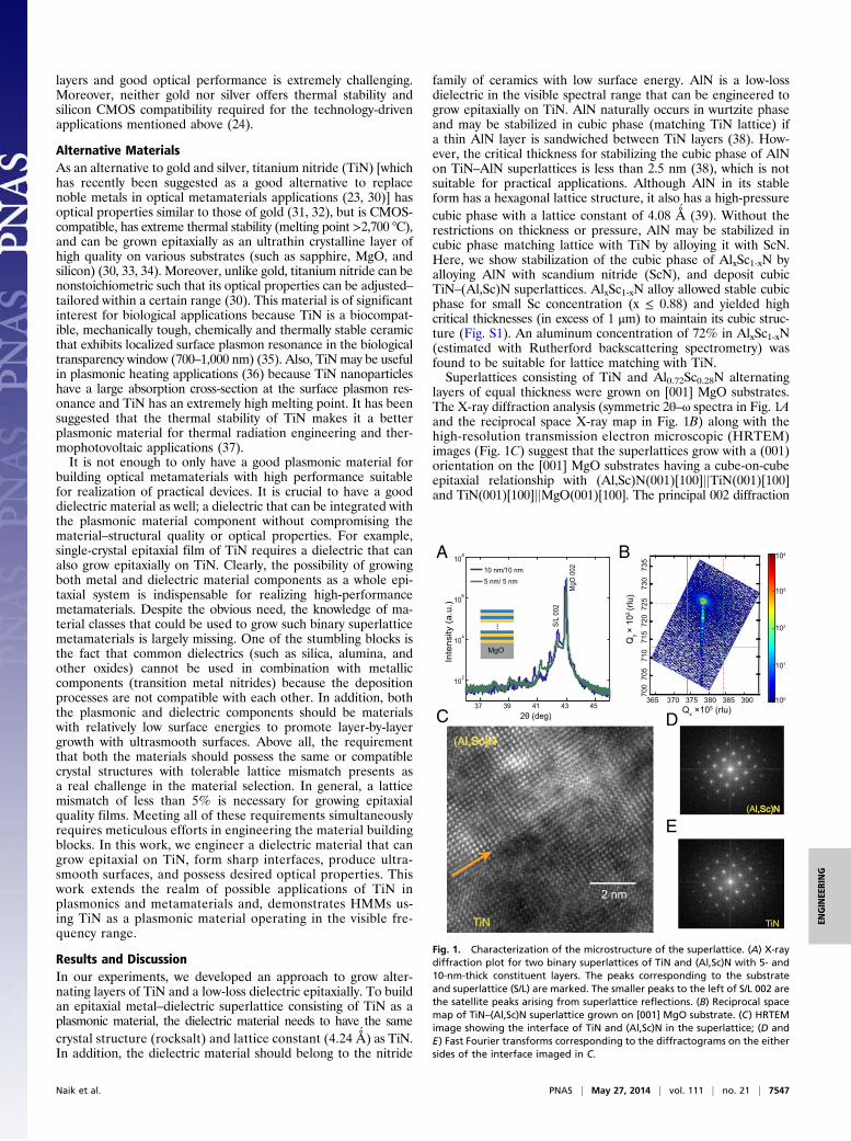
layers of equal thickness were grown on [001] MgO substrates.The X-ray diffraction analysis (symmetric 2θ–ω spectra in Fig. 1Aand the reciprocal space X-ray map in Fig. 1B) along with thehigh-resolution transmission electron microscopic (HRTEM)images (Fig. 1C) suggest that the superlattices grow with a (001)orientation on the [001] MgO substrates having a cube-on-cubeepitaxial relationship with (Al,Sc)N(001)[100]jjTiN(001)[100]and TiN(001)[100]jjMgO(001)[100]. The principal 002 diffraction
A B
C D
E
365 370 375 380 385 390Qx ×105 (rlu)
700
705
71
0 7
15 7
20 7
25
730
73
5
Qy ×
105 (r
lu)
100
101
102
103
104
(Al,Sc)Nl,Sc)N
TiN
2 nm
(Al,Sc)Nl,Sc)N
TiN
37 39 41 43 45
102
104
106
108
2θ (deg)
Inte
nsity
(a.u
.)
10 nm/10 nm5 nm/ 5 nm
MgO
002
S/L
002
MgO
Fig. 1. Characterization of the microstructure of the superlattice. (A) X-raydiffraction plot for two binary superlattices of TiN and (Al,Sc)N with 5- and10-nm-thick constituent layers. The peaks corresponding to the substrateand superlattice (S/L) are marked. The smaller peaks to the left of S/L 002 arethe satellite peaks arising from superlattice reflections. (B) Reciprocal spacemap of TiN–(Al,Sc)N superlattice grown on [001] MgO substrate. (C) HRTEMimage showing the interface of TiN and (Al,Sc)N in the superlattice; (D andE) Fast Fourier transforms corresponding to the diffractograms on the eithersides of the interface imaged in C.
Naik et al. PNAS | May 27, 2014 | vol. 111 | no. 21 | 7547
ENGINEE
RING
peak is located at 2θ = 42.4°, suggesting an out-of-plane latticeconstant of 4.25 �Å. Strong satellite fringes due to the X-rayinterference at metal–dielectric interfaces are clearly visible (inFig. 1 A and B), indicating that the interfaces are sharp andabrupt. This conclusion was further confirmed by the TEMimages. The full width at half maximum of the rocking curve(ω-scan) has a very small value of 0.065°, suggesting a smalldegree of mosaicity. The vertical alignment of the main 024peak of the superlattice, the substrate (MgO), and the satellitefringes in the reciprocal space X-ray map indicate that thesuperlattices are pesudomorphic, i.e., the in-plane lattice con-stant of the constituent TiN and (Al,Sc)N layers are identical tothat of MgO (4.21 �Å). In the out-of-plane direction the TiNlayers have a lattice constant of 4.23�Å, which is very close to itsbulk value of 4.24 �Å, whereas the (Al,Sc)N layers have an out-of-plane lattice constant of 4.26 �Å.The optical properties of the superlattice consisting of 5-nm-
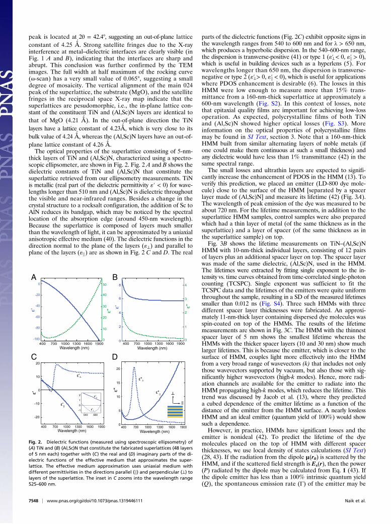
thick layers of TiN and (Al,Sc)N, characterized using a spectro-scopic ellipsometer, are shown in Fig. 2. Fig. 2 A and B shows thedielectric constants of TiN and (Al,Sc)N that constitute thesuperlattice retrieved from our ellipsometry measurements. TiNis metallic (real part of the dielectric permittivity «′ < 0) for wave-lengths longer than 510 nm and (Al,Sc)N is dielectric throughoutthe visible and near-infrared ranges. Besides a change in thecrystal structure to a rocksalt configuration, the addition of Sc toAlN reduces its bandgap, which may be noticed by the spectrallocation of the absorption edge (around 450-nm wavelength).Because the superlattice is composed of layers much smallerthan the wavelength of light, it can be approximated by a uniaxialanisotropic effective medium (40). The dielectric functions in thedirection normal to the plane of the layers («⊥) and parallel toplane of the layers («k) are as shown in Fig. 2 C and D. The real
parts of the dielectric functions (Fig. 2C) exhibit opposite signs inthe wavelength ranges from 540 to 600 nm and for λ > 650 nm,which produces a hyperbolic dispersion. In the 540–600-nm range,the dispersion is transverse-positive (41) or type 1 («⊥′ < 0, «k′ > 0),which is useful in building devices such as a hyperlens (5). Forwavelengths longer than 650 nm, the dispersion is transverse-negative or type 2 («⊥′ > 0, «k′ < 0), which is useful for applicationswhere PDOS enhancement is desirable (6). The losses in thisHMM were low enough to measure more than 15% trans-mittance from a 160-nm-thick superlattice at approximately a600-nm wavelength (Fig. S2). In this context of losses, notethat epitaxial quality films are important for achieving low-lossoperation. As expected, polycrystalline films of both TiNand (Al,Sc)N showed higher optical losses (Fig. S3). Moreinformation on the optical properties of polycrystalline filmsmay be found in SI Text, section 3. Note that a 160-nm-thickHMM built from similar alternating layers of noble metals (ifone could make them continuous at such a small thickness) andany dielectric would have less than 1% transmittance (42) in thesame spectral range.The small losses and ultrathin layers are expected to signifi-
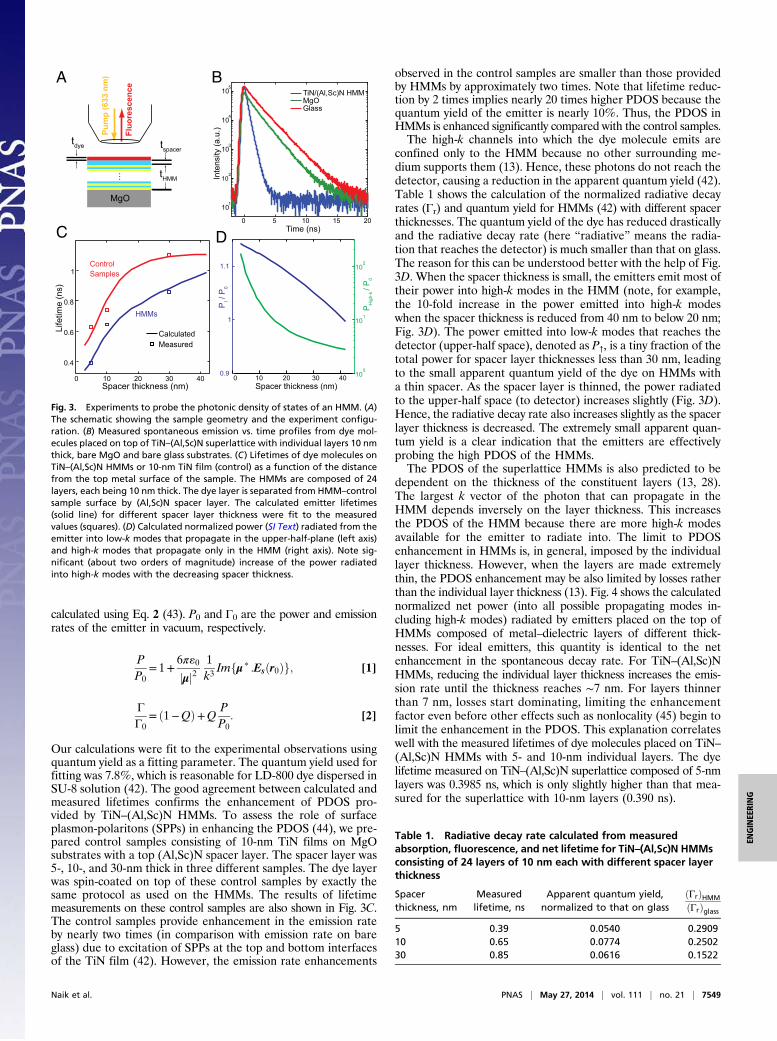
cantly increase the enhancement of PDOS in the HMM (13). Toverify this prediction, we placed an emitter (LD-800 dye mole-cule) close to the surface of the HMM [separated by a spacerlayer made of (Al,Sc)N] and measure its lifetime (42) (Fig. 3A).The wavelength of peak emission of the dye was measured to beabout 720 nm. For the lifetime measurements, in addition to thesuperlattice HMM samples, control samples were also preparedwhich had a thin layer of metal (of the same thickness as in thesuperlattice) and a layer of spacer (of the same thickness as inthe superlattice sample) on top.Fig. 3B shows the lifetime measurements on TiN–(Al,Sc)N
HMM with 10-nm-thick individual layers, consisting of 12 pairsof layers plus an additional spacer layer on top. The spacer layerwas made of the same dielectric, (Al,Sc)N, used in the HMM.The lifetimes were extracted by fitting single exponent to the in-tensity vs. time curves obtained from time-correlated single-photoncounting (TCSPC). Single exponent was sufficient to fit theTCSPC data and the lifetimes of the emitters were quite uniformthroughout the sample, resulting in a SD of the measured lifetimessmaller than 0.012 ns (Fig. S4). Three such HMMs with threedifferent spacer layer thicknesses were fabricated. An approxi-mately 11-nm-thick layer containing dispersed dye molecules wasspin-coated on top of the HMMs. The results of the lifetimemeasurements are shown in Fig. 3C. The HMM with the thinnestspacer layer of 5 nm shows the smallest lifetime whereas theHMMs with the thicker spacer layers (10 and 30 nm) show muchlarger lifetimes. This is because the emitter, which is closer to thesurface of HMM, couples light more effectively into the HMMfrom a very broad range of wavevectors (k) that includes not onlythose wavevectors supported by vacuum, but also those with sig-nificantly higher wavevectors (high-k modes). Hence, more radi-ation channels are available for the emitter to radiate into theHMM propagating high-k modes, which reduces the lifetime. Thistrend was discussed by Jacob et al. (13), where they predicteda cubed dependence of the emitter lifetime as a function of thedistance of the emitter from the HMM surface. A nearly losslessHMM and an ideal emitter (quantum yield of 100%) would showsuch a dependence.However, in practice, HMMs have significant losses and the
emitter is nonideal (42). To predict the lifetime of the dyemolecules placed on the top of HMM with different spacerthicknesses, we use local density of states calculations (SI Text)(28, 43). If the radiation from the dipole μ(r0) is scattered by theHMM, and if the scattered field strength is Es(r), then the power(P) radiated by the dipole may be calculated from Eq. 1 (43). Ifthe dipole emitter has less than a 100% intrinsic quantum yield(Q), the spontaneous emission rate (Γ) of the emitter may be
-100
-80
-60
-40
-20
0
0
10
20
30
40
50
ε"ε'
Wavelength (nm)400 700 1000 1300 1600 1900 400 700 1000 1300 1600 1900
0
2
4
6
8
Wavelength (nm)
ε'
0
1
2
3
4
ε"
400 700 1000 1300 1600 1900
-20
-10
0
10
20
Wavelength (nm)
ε'
ε'┴
ε'||
400 700 1000 1300 1600 19000
5
10
15
20
Wavelength (nm)
ε"
ε"┴
ε"|| ┴
||
A B
C D
540 580
-1
0
1
2
ε'┴
ε'||
Fig. 2. Dielectric functions (measured using spectroscopic ellipsometry) of(A) TiN and (B) (Al,Sc)N that constitute the fabricated superlattices (48 layersof 5 nm each) together with (C) the real and (D) imaginary parts of the di-electric functions of the effective medium that approximates the super-lattice. The effective medium approximation uses uniaxial medium withdifferent permittivities in the directions parallel (k) and perpendicular (⊥) tolayers of the superlattice. The inset in C zooms into the wavelength range525–600 nm.
7548 | www.pnas.org/cgi/doi/10.1073/pnas.1319446111 Naik et al.
calculated using Eq. 2 (43). P0 and Γ0 are the power and emissionrates of the emitter in vacuum, respectively.
PP0
= 1+6π«0jμj2
1k3
Imfμ p :Esðr0Þg; [1]
ΓΓ0
= ð1−QÞ+QPP0: [2]
Our calculations were fit to the experimental observations usingquantum yield as a fitting parameter. The quantum yield used forfitting was 7.8%, which is reasonable for LD-800 dye dispersed inSU-8 solution (42). The good agreement between calculated andmeasured lifetimes confirms the enhancement of PDOS pro-vided by TiN–(Al,Sc)N HMMs. To assess the role of surfaceplasmon-polaritons (SPPs) in enhancing the PDOS (44), we pre-pared control samples consisting of 10-nm TiN films on MgOsubstrates with a top (Al,Sc)N spacer layer. The spacer layer was5-, 10-, and 30-nm thick in three different samples. The dye layerwas spin-coated on top of these control samples by exactly thesame protocol as used on the HMMs. The results of lifetimemeasurements on these control samples are also shown in Fig. 3C.The control samples provide enhancement in the emission rateby nearly two times (in comparison with emission rate on bareglass) due to excitation of SPPs at the top and bottom interfacesof the TiN film (42). However, the emission rate enhancements
observed in the control samples are smaller than those providedby HMMs by approximately two times. Note that lifetime reduc-tion by 2 times implies nearly 20 times higher PDOS because thequantum yield of the emitter is nearly 10%. Thus, the PDOS inHMMs is enhanced significantly compared with the control samples.The high-k channels into which the dye molecule emits are
confined only to the HMM because no other surrounding me-dium supports them (13). Hence, these photons do not reach thedetector, causing a reduction in the apparent quantum yield (42).Table 1 shows the calculation of the normalized radiative decayrates (Γr) and quantum yield for HMMs (42) with different spacerthicknesses. The quantum yield of the dye has reduced drasticallyand the radiative decay rate (here “radiative” means the radia-tion that reaches the detector) is much smaller than that on glass.The reason for this can be understood better with the help of Fig.3D. When the spacer thickness is small, the emitters emit most oftheir power into high-k modes in the HMM (note, for example,the 10-fold increase in the power emitted into high-k modeswhen the spacer thickness is reduced from 40 nm to below 20 nm;Fig. 3D). The power emitted into low-k modes that reaches thedetector (upper-half space), denoted as P↑, is a tiny fraction of thetotal power for spacer layer thicknesses less than 30 nm, leadingto the small apparent quantum yield of the dye on HMMs witha thin spacer. As the spacer layer is thinned, the power radiatedto the upper-half space (to detector) increases slightly (Fig. 3D).Hence, the radiative decay rate also increases slightly as the spacerlayer thickness is decreased. The extremely small apparent quan-tum yield is a clear indication that the emitters are effectivelyprobing the high PDOS of the HMMs.The PDOS of the superlattice HMMs is also predicted to be
dependent on the thickness of the constituent layers (13, 28).The largest k vector of the photon that can propagate in theHMM depends inversely on the layer thickness. This increasesthe PDOS of the HMM because there are more high-k modesavailable for the emitter to radiate into. The limit to PDOSenhancement in HMMs is, in general, imposed by the individuallayer thickness. However, when the layers are made extremelythin, the PDOS enhancement may be also limited by losses ratherthan the individual layer thickness (13). Fig. 4 shows the calculatednormalized net power (into all possible propagating modes in-cluding high-k modes) radiated by emitters placed on the top ofHMMs composed of metal–dielectric layers of different thick-nesses. For ideal emitters, this quantity is identical to the netenhancement in the spontaneous decay rate. For TiN–(Al,Sc)NHMMs, reducing the individual layer thickness increases the emis-sion rate until the thickness reaches ∼7 nm. For layers thinnerthan 7 nm, losses start dominating, limiting the enhancementfactor even before other effects such as nonlocality (45) begin tolimit the enhancement in the PDOS. This explanation correlateswell with the measured lifetimes of dye molecules placed on TiN–(Al,Sc)N HMMs with 5- and 10-nm individual layers. The dyelifetime measured on TiN–(Al,Sc)N superlattice composed of 5-nmlayers was 0.3985 ns, which is only slightly higher than that mea-sured for the superlattice with 10-nm layers (0.390 ns).
Table 1. Radiative decay rate calculated from measuredabsorption, fluorescence, and net lifetime for TiN–(Al,Sc)N HMMsconsisting of 24 layers of 10 nm each with different spacer layerthickness
Spacerthickness, nm
Measuredlifetime, ns
Apparent quantum yield,normalized to that on glass
ðΓrÞHMM
ðΓrÞglass5 0.39 0.0540 0.290910 0.65 0.0774 0.250230 0.85 0.0616 0.1522
0 5 10 15 20
101
102
103
104
105
Time (ns)In
tens
ity (a
.u.)
TiN/(Al,Sc)N HMMMgOGlass
MgO
tHMM
tspacertdye
Pum
p (6
33 n
m)
Fluo
resc
ence
A B
C D
0.9
1
1.1
P ↑ / P
0
0 10 20 30 40 100
101
102
P Hig
h-k / P
0
Spacer thickness (nm)0 10 20 30 40
0.4
0.6
0.8
1
Spacer thickness (nm)
Life
time
(ns)
HMMs
ControlSamples
CalculatedMeasured
Fig. 3. Experiments to probe the photonic density of states of an HMM. (A)The schematic showing the sample geometry and the experiment configu-ration. (B) Measured spontaneous emission vs. time profiles from dye mol-ecules placed on top of TiN–(Al,Sc)N superlattice with individual layers 10 nmthick, bare MgO and bare glass substrates. (C) Lifetimes of dye molecules onTiN–(Al,Sc)N HMMs or 10-nm TiN film (control) as a function of the distancefrom the top metal surface of the sample. The HMMs are composed of 24layers, each being 10 nm thick. The dye layer is separated from HMM–controlsample surface by (Al,Sc)N spacer layer. The calculated emitter lifetimes(solid line) for different spacer layer thickness were fit to the measuredvalues (squares). (D) Calculated normalized power (SI Text) radiated from theemitter into low-k modes that propagate in the upper-half-plane (left axis)and high-k modes that propagate only in the HMM (right axis). Note sig-nificant (about two orders of magnitude) increase of the power radiatedinto high-k modes with the decreasing spacer thickness.
Naik et al. PNAS | May 27, 2014 | vol. 111 | no. 21 | 7549
ENGINEE
RING
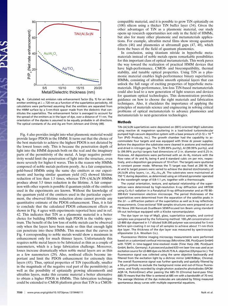
Fig. 4 also provides insight into what plasmonic material wouldprovide larger PDOS in the HMM. It turns out that the choice ofthe best materials to achieve the highest PDOS is not dictated bythe lowest losses only. This is because the penetration depth oflight into the HMM depends both on the real and the imaginaryparts of the permittivity of the metal. A large negative permit-tivity would limit the penetration of light into the structure, evenmore severely for higher-k waves. This is the reason why HMMscomposed of noble metals perform poorly. As a fair comparison,gold-based HMMs using the same dye emitters as our experi-ments and having similar quantum yield (42) showed lifetimereduction of less than 1.5 times, whereas TiN–(Al,Sc)N HMMsproduce about 5.5 times reduction in the lifetime. A fair compar-ison with other reports is possible if quantum yields of the emittersused in the experiments are known. Without the knowledge ofthe quantum yield of the emitters used in the particular experi-ment, the observed lifetime reduction alone cannot provide anyquantitative estimate of the PDOS enhancement. Thus, it is fairto conclude that the calculated PDOS enhancement effects asshown in Fig. 4 agree with experiments reported here and in ref.42. This indicates that TiN as a plasmonic material is a betterchoice for building HMMs with high PDOS in the visible spec-trum. The benefit of the low loss of noble metals can be observedonly when the layers have been made so thin that enough lightcan penetrate into these HMMs. This means that the curves inFig. 4 corresponding to noble metals would show a maximum inenhancement only for much thinner layers. Unfortunately thisrequires noble metal layers to be fabricated as thin as a couple ofnanometers, which is a large fabrication challenge. Moreover,losses increase dramatically when noble metal layers are as thinas a few nanometers (29). Also, nonlocal effects become im-portant and limit the PDOS enhancement for extremely thinlayers (45). Thus, optical properties of TiN (specifically, smallerin the magnitude of the negative real part of the permittivity) aswell as the possibility of epitaxially growing ultrasmooth andultrathin layers, make this ceramic material a better alternativeto obtain a higher PDOS in HMMs. This fabrication techniquecould be extended to CMOS platform given that TiN is a CMOS-
compatible material, and it is possible to grow TiN epitaxially on(100) silicon using a thicker TiN buffer layer (34). Given theother advantages of TiN as a plasmonic material, our studyopens up research opportunities not only in the field of HMMs,but also for many other plasmonic and metamaterials applica-tions. For example, ultrathin metal films show strong quantumeffects (46) and plasmonics at ultrasmall gaps (47, 48), whichform the bases of the field of quantum plasmonics.In conclusion, using titanium nitride in hyperbolic meta-
materials instead of noble metals opens remarkable possibilitiesfor this important class of optical metamaterials. This work pavesthe way toward the realization of practical HMM devices thathave high-performance, CMOS- and biocompatibility, thermalstability, and tunable optical properties. Using TiN as a plas-monic material enables high-performance binary superlatticeHMMs, consisting of ultrathin smooth epitaxial layers that canunlock the full range of exciting properties of hyperbolic meta-materials. High-performance, low-loss TiN-based metamaterialscould also lead to a new generation of light sources and devicesfor quantum optical technologies. This demonstration providesguidance on how to choose the right materials and fabricationtechniques. Also, it elucidates the importance of applying theprinciples of materials science and engineering in solving criticalproblems of optical metamaterials to advance plasmonics andmetamaterials to next-generation technologies.
MethodsTiN–(Al,Sc)N superlattices were deposited on (001)-oriented MgO substratesusing reactive dc magnetron sputtering in a load-locked turbomolecularpumped high-vacuum deposition system with a base pressure of (2–5) × 10−8
Torr (PVD Products, Inc.). The growth chamber had the capability to ac-commodate four targets and was equipped with three dc power supplies.Before the deposition the substrates were cleaned in acetone and methanoland dried in nitrogen gas. The Ti (99.99% purity), Al (99.99% purity), andSc (99.99% purity) targets had dimensions of 2-in. diameter and 0.25-in.thickness. All depositions were performed with an Ar–N2 mixture with theflow rates of Ar and N2 being 4 and 6 standard cubic cm per min, respec-tively, and a deposition gas pressure of 10 mTorr. The targets were sputteredin constant power mode. Whereas the Ti target was fixed at 200 W, theAl and Sc target powers were varied to achieve the desired stoichiometry of(Al,Sc)N alloy layers, i.e., Al0.7Sc0.3N. The substrates were maintained at750 °C during deposition, as determined using an infrared pyrometer operatedin the wavelength range of 0.8–1.1 μm, together with a thermocouple.
The crystal orientation, texture, and epitaxial relationship of the super-lattices were determined by high-resolution X-ray diffraction and HRTEMusing Cu Kα1 radiation in a Panalytical X-ray diffractrometer and an FEI 80–300-KeV transmission electron microscope. The period thicknesses of thesuperlattices were determined from the separation of the satellite peaks inthe 2θ−ω diffraction pattern of the superlattice as well as X-ray reflectivitymeasurements. Cross-sectional TEM samples structures were prepared on anFEI Nova 200 NanoLab DualBeam SEM/Focused Ion Beam using standardlift-out technique equipped with a Klocke nanomanipulator.
The dye layer on top of MgO, glass, superlattice samples, and controlsamples was prepared by the following method: 100-μM concentration ofLD-800 dye dispersed in 1:7 diluted SU8-200 polymer was sonicated for 5 minbefore spin-coating it on top of all samples to achieve about 11-nm-thickdye layer. The thickness of the dye layer was measured by spectroscopicellipsometer (J.A. Woollam Co.).
Fluorescence lifetime imaging microscopy measurements were performedbased on a customized confocal microscopy (Microtime 200, PicoQuant GmbH)with TCSPC in time-tagged time-resolved mode (Time Harp 200, PicoQuantGmbH, Berlin, Germany). A picosecond pulsed 633-nm laser line was used as anexcitation source for LD-800 dyes via 50×/0.75N.A. objective (Olympus Inc.). Thefluorescence signal was collected using the same objective backwardly andfiltered from the excitation light by a dichroic mirror (z467/638rpc, Chroma).The overall fluorescence signal was further spectrally and spatially filtered bya 50-μm pinhole to exclude the background noise and out-of-focus fluores-cence, and finally recorded by single-photon avalanche photodiodes (SPCM-AQR-14, PerkinElmer) after passing the 685-70 (Chroma) band-pass filter(685-70 means that the filter is centered at 685 nm with a bandwidth of 70 nm).The average lifetimes of the dye molecules are calculated by fitting measuredspontaneous decay curves with multiple exponential equations.
5/5 10/10 15/15 20/200
20
40
60
80
Metal/Dielectric thickness (nm)
P/P
0 (N
et ra
te e
nhan
cem
ent)
TiN/(Al,Sc)N
Au/Al2O3
Ag/TiO2
Fig. 4. Calculated net emission rate enhancement factor (Eq. 1) for an idealemitter emitting at λ = 720 nm as a function of the superlattice periodicity. Allcalculations were performed assuming that the emitters are separated fromthe HMM surface by a 5-nm-thick spacer made from the dielectric that con-stitutes the superlattice. The enhancement factor is averaged to account forthe spread of the emitters as in the layer of dye, over a distance of 11 nm. Theorientation of the dipoles is assumed to be equally probable in all directions.The optical constants of Au and Ag are from Johnson and Christy (49).
7550 | www.pnas.org/cgi/doi/10.1073/pnas.1319446111 Naik et al.

ACKNOWLEDGMENTS. G.V.N., V.M.S., and A.B. acknowledge numerous usefuldiscussions with members of the V.M.S. and A.B. research groups. They also
acknowledge support from Army Research Office Grant 57981-PH (W911NF-11-1-0359) and National Science Foundation Grant DMR-1120923.
1. Pendry JB, Schurig D, Smith DR (2006) Controlling electromagnetic fields. Science312(5781):1780–1782.
2. Shalaev VM (2008) Physics. Transforming light. Science 322(5900):384–386.3. Smith DR, Schurig D (2003) Electromagnetic wave propagation in media with in-
definite permittivity and permeability tensors. Phys Rev Lett 90(7):077405.4. Podolskiy VA, Narimanov EE (2005) Strongly anisotropic waveguide as a nonmagnetic
left-handed system. Phys Rev B 71(20):201101.5. Jacob Z, Alekseyev LV, Narimanov E (2006) Optical Hyperlens: Far-field imaging be-
yond the diffraction limit. Opt Express 14(18):8247–8256.6. Cortes C, Newman W, Molesky S, Jacob Z (2012) Quantum nanophotonics using hy-
perbolic metamaterials. J Opt 14(6):063001.7. Jacob Z, Shalaev VM (2011) Physics. Plasmonics goes quantum. Science 334(6055):
463–464.8. Salandrino A, Engheta N (2006) Far-field subdiffraction optical microscopy using meta-
material crystals: Theory and simulations. Phys Rev B 74(7):075103.9. Liu Z, Lee H, Xiong Y, Sun C, Zhang X (2007) Far-field optical hyperlens magnifying
sub-diffraction-limited objects. Science 315(5819):1686.10. Rho J, et al. (2010) Spherical hyperlens for two-dimensional sub-diffractional imaging
at visible frequencies. Nat Commun 1:143.11. Yang X, Yao J, Rho J, Yin X, Zhang X (2012) Experimental realization of three-dimensional
indefinite cavities at the nanoscale with anomalous scaling laws. Nat Photonics6:450–454.
12. Kabashin AV, et al. (2009) Plasmonic nanorod metamaterials for biosensing. NatMater 8(11):867–871.
13. Jacob Z, Smolyaninov II, Narimanov EE (2012) Broadband Purcell effect: Radiativedecay engineering with metamaterials. Appl Phys Lett 100(18):181105.
14. Jacob Z, et al. (2010) Engineering photonic density of states using metamaterials.Appl Phys B 100(1):215–218.
15. Noginov MA, et al. (2010) Controlling spontaneous emission with metamaterials. OptLett 35(11):1863–1865.
16. Krishnamoorthy HNS, Jacob Z, Narimanov E, Kretzschmar I, Menon VM (2012) To-pological transitions in metamaterials. Science 336(6078):205–209.
17. Tumkur T, et al. (2011) Control of spontaneous emission in a volume of functionalizedhyperbolic metamaterial. Appl Phys Lett 99(15):151115.
18. Lounis B, Orrit M (2005) Single-photon sources. Rep Prog Phys 68(5):1129–1179.19. Shalaginov M, et al. (2013) Broadband enhancement of spontaneous emission from
nitrogen-vacancy centers in nanodiamonds by hyperbolic metamaterials. Appl PhysLett 102(17):173114.
20. Newman WD, Cortes CL, Jacob Z (2013) Enhanced and directional single-photonemission in hyperbolic metamaterials. JOSA B 30(4):766–775.
21. Guo Y, Cortes CL, Molesky S, Jacob Z (2012) Broadband super-Planckian thermalemission from hyperbolic metamaterials. Appl Phys Lett 101(13):131106.
22. Narimanov EE, Smolyaninov II (2011) Beyond Stefan-Boltzmann Law: Thermal hyper-conductivity. arXiv:1109.5444.
23. Naik GV, Kim J, Boltasseva A (2011) Oxides and nitrides as alternative plasmonicmaterials in the optical range. Opt Mater Express 1(6):1090–1099.
24. Naik GV, Shalaev VM, Boltasseva A (2013) Alternative plasmonic materials: Beyondgold and silver. Adv Mater 25(24):3264–3294.
25. Elser J, Wangberg R, Podolskiy VA, Narimanov EE (2006) Nanowire metamaterialswith extreme optical anisotropy. Appl Phys Lett 89(26):261102–261103.
26. Yao J, et al. (2008) Optical negative refraction in bulk metamaterials of nanowires.Science 321(5891):930.
27. Noginov M, et al. (2009) Bulk photonic metamaterial with hyperbolic dispersion. Appl
Phys Lett 94(15):151105.28. Kidwai O, Zhukovsky SV, Sipe JE (2011) Dipole radiation near hyperbolic meta-
materials: Applicability of effective-medium approximation. Opt Lett 36(13):2530–2532.29. Drachev VP, et al. (2008) The Ag dielectric function in plasmonic metamaterials. Opt
Express 16(2):1186–1195.30. Naik GV, et al. (2012) Titanium nitride as a plasmonic material for visible and near-
infrared wavelengths. Opt Mater Express 2(4):478–489.31. Hibbins AP, Sambles JR, Lawrence CR (1998) Surface plasmon-polariton study of the
optical dielectric function of titanium nitride. J Mod Opt 45(10):2051–2062.32. Chen N, et al. (2011) Excitation of surface plasma wave at TiN/air interface in the
Kretschmann geometry. J Appl Phys 109(4):043104.33. Hultman L, Barnett S, Sundgren J-E, Greene J (1988) Growth of epitaxial TiN films
deposited on MgO (100) by reactive magnetron sputtering: The role of low-energy
ion irradiation during deposition. J Cryst Growth 92(3):639–656.34. Narayan J, et al. (1992) Epitaxial growth of TiN films on (100) silicon substrates by laser
physical vapor deposition. Appl Phys Lett 61(11):1290–1292.35. Guler U, Naik G, Boltasseva A, Shalaev V, Kildishev A (2012) Performance analysis
of nitride alternative plasmonic materials for localized surface plasmon applications.
Appl Phys B 107(2):285–291.36. Neumann O, et al. (2013) Solar vapor generation enabled by nanoparticles. ACS Nano
7(1):42–49.37. Molesky S, Dewalt CJ, Jacob Z (2013) High temperature epsilon-near-zero and epsilon-
near-pole metamaterial emitters for thermophotovoltaics. Opt Express 21(101, Suppl
1):A96–A110.38. Madan A, et al. (1997) Stabilization of cubic AlN in epitaxial AlN/TiN superlattices.
Phys Rev Lett 78(9):1743–1746.39. Uehara S, et al. (1997) Equation of state of the rocksalt phase of III–V nitrides to 72
GPa or higher. J Phys Chem Solids 58(12):2093–2099.40. Rytov S (1956) Electromagnetic properties of a finely stratified medium. Sov Phys JETP
2(3):466–475.41. Naik GV, Liu J, Kildishev AV, Shalaev VM, Boltasseva A (2012) Demonstration of
Al:ZnO as a plasmonic component for near-infrared metamaterials. Proc Natl Acad Sci
USA 109(23):8834–8838.42. Kim J, et al. (2012) Improving the radiative decay rate for dye molecules with hy-
perbolic metamaterials. Opt Express 20(7):8100–8116.43. Novotny L, Hecht B (2006) Principles of Nano-Optics (Cambridge Univ Press, New
Delhi, India).44. Vuckovic J, Loncar M, Scherer A (2000) Surface plasmon enhanced light-emitting di-
ode. IEEE J Quant Electron 36(10):1131–1144.45. Yan W, Wubs M, Mortensen NA (2012) Hyperbolic metamaterials: Nonlocal response
regularizes broadband supersingularity. Phys Rev B 86(20):205429.46. Scholl JA, Koh AL, Dionne JA (2012) Quantum plasmon resonances of individual
metallic nanoparticles. Nature 483(7390):421–427.47. Ciracì C, et al. (2012) Probing the ultimate limits of plasmonic enhancement. Science
337(6098):1072–1074.48. Savage KJ, et al. (2012) Revealing the quantum regime in tunnelling plasmonics.
Nature 491(7425):574–577.49. Johnson PB, Christy R (1972) Optical constants of the noble metals. Phys Rev B 6(12):
4370–4379.
Naik et al. PNAS | May 27, 2014 | vol. 111 | no. 21 | 7551
ENGINEE
RING
Related Documents