ENT SENIOR DESIGN PROJECT REPORT Hydroponic Control System Submitted to: Professor Cooney Engineering Technology Department By: Andrew McNeely August 5, 2017

Welcome message from author
This document is posted to help you gain knowledge. Please leave a comment to let me know what you think about it! Share it to your friends and learn new things together.
Transcript

ENT SENIOR DESIGN PROJECT REPORT
Hydroponic Control System
Submitted to: Professor Cooney
Engineering Technology Department
By: Andrew McNeely
August 5, 2017

Issued By:
Approved By:
Effective Date: 8/05/2017
Page 2 of 23
Andrew McNeely
Document No.: 1
Version: 1.00
Hydroponic Control System
ABSTRACT The goal of this project is to design and construct a hydroponic control system. The control system will process signals from the required inputs and control output devices based on operational criteria. The control system will display the amounts of water and nutrients that need to be added on a daily basis to maintain a proper growing environment. A daily chemical test is required so these readings can be obtained. The desired nutritional specs are provided by Emerald Harvest Nutrient Series Feeding Chart. The system consist of 3 chemicals, Grow, Bloom, and Micro. The ratios of these 3 chemicals change on a weekly basis during the 16 week grow cycle. The system will continuously monitor the humidity of the grow area and cycle a humidifier to maintain the area within certain specs. Since the system is designed to be indoors, a way to control temperature is not needed. The grow lights are designed to supplement natural light and therefore the system needed to be placed near a south facing window. With minimal user interaction, the system should be able to provide adequate grow environment for up to 5 small herbs over an entire grow cycle. After a grow cycle is complete, the system is ready to start all over again.

Issued By:
Approved By:
Effective Date: 8/05/2017
Page 3 of 23
Andrew McNeely
Document No.: 1
Version: 1.00
Hydroponic Control System
TABLE OF CONTENTS: ABSTRACT REVISION HISTORY
1. INTRODUCTION 2. REFERENCED DOCUMENTS 3. SYSTEM-WIDE DECISIONS 4. SYSTEM ARCHITECTURLAL DESIGN 5. SYSTEM SETUP 6. SYSTEM OPERATION 7. CONCLUSION AND RECOMMENDATIONS
APPENDIX LIST OF FIGURES: Figure 1 - Nutrient Film Technique Figure 2 - Relay Control Board Schematic Figure 3 - Relay Control Board Layout Figure 4 - Switch Mode Power Supply Schematic Figure 5 - Switch Mode Power Supply Layout Figure 6 - User Interface Schematic Figure 7 - User Interface Layout Figure 8 - Software Overview Figure 9 - Display Option 1 Figure 10 - Display Option 2 Figure 11 - Display Option 3 Figure 12 - User Interface pushbuttons Figure 13 - Ultrasonic Timing Diagram Figure 14 - System One-line LIST OF TABLES: Table 1 - Reference Documents Table 2 - pH Sensor Calibration Table 3 - TDS Sensor Calibration

Issued By:
Approved By:
Effective Date: 8/05/2017
Page 4 of 23
Andrew McNeely
Document No.: 1
Version: 1.00
Hydroponic Control System
REVISION HISTORY
Date Initials Version Update Notes 2017.04.06 ARM 0.01 Initial Draft Version 2017.04.16 ARM 0.02 Added System setup and System Operation 2017.04.23 ARM 0.03 Updated humidifier specs 2017.05.15 ARM 0.04 Updated power supply schematic and layout 2017.06.24 ARM 0.05 Added User interface and Interface sections 2017.7.21 ARM 0.06 Added sections for final review 2017.08.05 ARM 1.00 Initial Release Version
IUPUI Information
This project was completed by Andrew McNeely as a Senior Design Capstone Project. The Capstone Project is a requirement to obtain a Bachelor’s of Science in Electrical Engineering Technology through the Indiana University-Purdue University of Indianapolis.

Issued By:
Approved By:
Effective Date: 8/05/2017
Page 5 of 23
Andrew McNeely
Document No.: 1
Version: 1.00
Hydroponic Control System
1. INTRODUCTION 1.1 Problem Statement
Due to the climate of central Indiana, I am unable to grow fresh vegetables and herbs year round. Using my knowledge gained in the field of electrical engineering technology, I am designing a control system for a hydroponic system that enables me to grow fresh herbs inside my house all year long. If this control system is shown to adequately control the grow environment of herbs, I have the ability to scale up the operation to include larger vegetables. 1.2 Key Terms
Hydroponics – The process of growing plants in a non-soil based media. Sand, gravel, or
water can be utilized as a median along with added nutrients. Nutrient film technique (NFT) – A hydroponic grow technique that places the roots of
growing plants directly in a slow moving stream of nutrient rich water. Potential of hydrogen (pH) – A scale to specify the acidity or basicity of a liquid solution. Total dissolved solids (TDS) – A measure of the amount of inorganic and organic
particles in water.
1.3 System Overview The technique used for this hydroponics system is a nutrient film technique. This type of system utilizes a reservoir to hold the excess nutrient rich water. This water is pumped through a trough and gravity drains back into the reservoir. The growing plants sit in the trough and the roots grow down into the water to receive the desired nutrients. The nutrient level of the water changes on a weekly basis based on which week of the grow cycle the system is in. The user actions to maintain the system include daily chemical test, addition of chemicals as displayed on screen, and maintaining water level of the reservoir.

Issued By:
Approved By:
Effective Date: 8/05/2017
Page 6 of 23
Andrew McNeely
Document No.: 1
Version: 1.00
Hydroponic Control System
Figure 1 - Nutrient Film Technique
2. REFERENCED DOCUMENTS
Table 1: Reference Documents
Title Document Reference Number
Appendix
Arduino Mega 2560 A000047 B AMOTEC LCD Module Specifications ADM1602K-NSW-FBS C LM2678 Simple Switcher Specifications lm2678 D AOSONG Temperature and humidity Module AM2301 E Ultrasonic Ranging Module HC-SR04 HCSR04 F Uxcell Hall Effect Water Flow Sensor Uxcell-Hall Effect Water Flow Sensor G SEN0161 pH Meter SEN0161 H DFR0300 Analog EC meter DFR0300 I Ultrasonic Humidifier Use & Care Manual A1HllCAzl1L J ActiveAQUA Instruction Manual aapw400 K Emerald Harvest 3 part nutrient series Feeding-Chart-GMB-3-Part L

Issued By:
Approved By:
Effective Date: 8/05/2017
Page 7 of 23
Andrew McNeely
Document No.: 1
Version: 1.00
Hydroponic Control System
3. SYSTEM-WIDE DESIGN
3.1 Design Trade Offs
The most significant design criterion for this project is the overall price of the final design. The project is personally funded therefore the price of each component within the project had to be minimized while still meeting functional specs. Goal for a finished product was to not exceed $500.
The system was designed to be placed in front of a standard window and have the ability to be moved from room to room as needed. This criterion limited the overall size of the frame to be no wider that two feet. The system can easily be broken down into 2 pieces, frame/controls and reservoir, for mobility.
The system was designed to assist the natural sunlight with grow lights. This allows for smaller grow lights to be implemented into the system.
I chose to use a standard 5 gallon bucket as the water reservoir. This meet both price and mobility criteria above. Due to the height of the reservoir, I needed the grow trough to be a minimum of 15 inches at its lowest point.
An Arduino Mega control board was used due to the price and abundant I/O. The system required more I/O than an Arduino Uno could manage.
The circulation pump decision was based on the overall pump height requirement of 15 inches. The pump had to provide enough flow through the tubing to a height of 15 inches.
Each output of the system (humidifier, circulation pump, mix pump, and grow lights) had to draw less than 5 amps during normal operation. This is due to the relays used to cycle power to the devices.
A humidifier had to have an on/off switch and not controlled by a microprocessor. I was unable to find one to meet this requirement and the ampacity draw from above so I had to modify the circuitry to make one meet this requirement.
3.2 Hardware
Each of the three printed circuit boards (excluding the Arduino Mega) were fully designed, tested, and implemented as part of the project design. Calculations can be found in appendix A.
Main processor of the system is an Arduino Mega 2560. Features of the control board include: 54 Digital I/O pins, 16 Analog pins, 40 mA per I/O pin, 7 -12 V DC Input Voltage. This board is used to process signals from all inputs and cycle power to all output devices as needed. The original idea for the user interface was to use an Arduino compatible PCB, 4Duino. It is designed to have all the same functionality and dimensions as the Arduino UNO with a built in touchscreen. The Arduino UNO would not meet my requirements for the

Issued By:
Approved By:
Effective Date: 8/05/2017
Page 8 of 23
Andrew McNeely
Document No.: 1
Version: 1.00
Hydroponic Control System
number of I/O due to the amount of inputs a display required. The 4Duinoe system would be able to meet these requirements since the display was built into the system. I was able to learn how to program the display gadgets and use them to control LEDs on a breadboard. Once I started combining all the code for the sensors I found out that the 4Duino PCB would not support the required libraries for the AM2301 and RTC modules. At this point I had to scrap the idea of using the 4Duino PCB and implement a standard Arduino MEGA.
Relay Control Board (RCB) – The primary function of the RCB is to energize a relay coil through a transistor circuit based on control signals from the processor. When the relay closes, contacts close to turn on the desired output device. Each relay is rated for up to 5 amps at 120 VAC. The RCB is designed with 1 plug which provides 12V, 5V, and GND connections to be jumpered from the user interface PCB. The secondary function of the RCB is to be a single connection point for all of the input sensors. Each sensor has a 5V pin, GND pin and either 1 or 2 signal pins, depending on the sensor. The sensor signals will pass through the RCB to the processor. The 5V and GND planes are designed with a jumper to allow isolation from the power supply, if desired. The system operates with the jumpers installed allowing for 1 connection point from the Arduino PCB to the 5V and GND planes.
Figure 2 - Relay Control Board Schematic

Issued By:
Approved By:
Effective Date: 8/05/2017
Page 9 of 23
Andrew McNeely
Document No.: 1
Version: 1.00
Hydroponic Control System
Figure 3 - Relay Control Board Layout
Switch mode power supply (SMPS) – The function of the SMPS is to convert typical house power (120 VAC) to usable 12VDC required to run the relays and processor. The Arduino MEGA can accept 6-20VDC but is recommended to stay within 7-12VDC for proper operation. The Arduino processor outputs a regulated 5VDC source to power the input sensors. A precise resistor feedback loop is required to supply the desired outputs. To allow for future adjustability, I placed a variable resistor in this feedback loop in lieu of standard resistors. The SMPS was originally designed to provide both, 12VDC and 5.5VDC regulated outputs. The 12V was designed to be utilized solely for the relay coil. The 5.5V was designed to provide input power to the 4Duino PCB, the original processor for the design. The 4Duino accepts a much narrower input voltage range than the Arduino MEGA. The 4Duino would have supplied the 5V needed to operate the input sensors. When the 4Duino was scrapped for certain reasons (described later in text), the 5.5V supply was no longer needed for the design. This happened after the PCB was printed and tested so the design was left in the documentation.

Issued By:
Approved By:
Effective Date: 8/05/2017
Page 10 of 23
Andrew McNeely
Document No.: 1
Version: 1.00
Hydroponic Control System
Figure 4 - Switch Mode Power Supply Schematic
Figure 5 - Switch Mode Power Supply Layout

Issued By:
Approved By:
Effective Date: 8/05/2017
Page 11 of 23
Andrew McNeely
Document No.: 1
Version: 1.00
Hydroponic Control System
User Interface – The function of the user interface PCB is to provide a means of control
for the user. It consist of a display that provides the user with visual information about the chemical make up of the water and the chemical requirements to meet specific setpoints. The user interface also provides 5 control push buttons. Two of these buttons perform control functions and three of the buttons are used to display various information needed for the system to function properly. The user interface contains 2 plugs on the board, one for the 12V supply from the power supply PCB and another plug to jumper 12V and 5V to the relay control board. The board contains a ground plane and a 5V plane, both of which are connected to the Arduino to allow for a complete path for all of the sensors and relay controls. Since this PCB was designed late in the design process, it’s dimensions are the same as the relay control board to allow for stacking in the control box. Holes in the user interface allow the user to clearly see indicating LEDs on the relay control board which sits directly below the user interface board.
Figure 6 - User Interface Schematic

Issued By:
Approved By:
Effective Date: 8/05/2017
Page 12 of 23
Andrew McNeely
Document No.: 1
Version: 1.00
Hydroponic Control System
Figure 7 - User Interface Layout
3.3 Software
The project code is written in C language using the Arduino IDE. Portions of the code are implemented using examples from the Arduino learning playground. Libraries that are utilized within the project code include:
LiquidCrystal.h – Used to properly display characters on the system display. Wire.h – Used to allow the use of the I2C bus. RTClib.h – Used to implement a real time clock. DHT.h – Used with the AM2301 temperature and humidity sensor.
The project code was written for each sensor individually and tested on an Arduino UNO prior to compiling it into a single project file. This allowed for easy troubleshooting and calibration of each sensor if required. The pH and Analog EC sensors are not considered industrial grade sensors and thus cannot be left in the liquid for long periods of time. This had to be considered when writing the project code. During my trial and error of working around this issue, I was able to implement a pre-test sequence that would hard code the system to a pre-test state. After a short time delay, required to allow the sensors time to soak in the reservoir, the system would automatically place itself in test mode, perform the test, and display the results.

Issued By:
Approved By:
Effective Date: 8/05/2017
Page 13 of 23
Andrew McNeely
Document No.: 1
Version: 1.00
Hydroponic Control System
3.4 Software Overview

Issued By:
Approved By:
Effective Date: 8/05/2017
Page 14 of 23
Andrew McNeely
Document No.: 1
Version: 1.00
Hydroponic Control System
Figure 8 - Software Overview

Issued By:
Approved By:
Effective Date: 8/05/2017
Page 15 of 23
Andrew McNeely
Document No.: 1
Version: 1.00
Hydroponic Control System
3.5 Interface
The system user will interface with the control system using the information provided on the display and the 5 pushbuttons provided on the user interface board. The display has 3 measurement pages to display the required data to allow for proper adjust of the system to maintain proper grow environment. Display option 1 shows the humidity of the surrounding environment and the level of the reservoir. The humidifier will cycle on at 60% and off at 70% humidity. The chemical test will be aborted if the level is below 9 inches. This is due to the length of the sensors in the reservoir.
Figure 9 - Display Option 1 After the initial chemical test, display option 2 will display the ppm and pH readings of the system. Prior to any test, this display window will show default readings as seen below.
Figure 10 - Display Option 2

Issued By:
Approved By:
Effective Date: 8/05/2017
Page 16 of 23
Andrew McNeely
Document No.: 1
Version: 1.00
Hydroponic Control System
Display option 3 will show the amount of each chemical that needs to be added to the system to maintain a proper chemical makeup of the water. The chemical makeup requirement changes weekly. These requirements are taken from Emerald Harvest 3 part nutient series. The amounts displayed are in milliLiters. If no chemical test has been completed on the system, display option 3 will not show any data.
Figure 11 - Display Option 3 The user inteface board has 5 pushbuttons used to control the system. From left to right: Mix Mode , Chemical Test Mode , Display 1, Display 2, Display 3
Figure 12 - User Interface pushbuttons The original plan was to implement the 4Duino with a built in touchscreen. When that idea was scrapped and I started implementing the Arduino MEGA as the processor, I needed a new way to display and control the system. I had access to a 2 * 16 LCD display that would be able to display enough information for the system to function correctly. I was able to design and test a circuit board that consisted of pushbutton circuitry and display hook-ups quickly. These actions allowed for my design to incorporate the required user interface.
4. SYSTEM ARCHITECTURAL DESIGN
4.1 System Inputs
SEN0161 Analog pH meter 5V operating voltage Range 0-14

Issued By:
Approved By:
Effective Date: 8/05/2017
Page 17 of 23
Andrew McNeely
Document No.: 1
Version: 1.00
Hydroponic Control System
Accuracy + 0.1 Response time < 1 min Potentiometer adjustable gain
Since the pH sensor is a linear sensor it could be calibrated by obtaining a few data points and creating a trend line. The below graph shows the test points and the resulting trend line. This equation was used in the project code to determine the pH of the water system.
Table 2 - pH Sensor Calibration
Gravity: Analog Electrical Conductivity (EC) Sensor 5V operating voltage Range 1ms/cm – 20ms/cm (640-1280 ppm) Accuracy < + 10%
Since the EC sensor is a linear sensor it could be calibrated by obtaining a few data points and creating a trend line. The below graph shows the test points and the resulting trend line. This equation was used in the project code to determine the TDS of the water system. Due to the length of the pH and EC sensors, the height of the reservoir needs to be above 9 inches for a chemical test to run successfully. If the level is below 9 inches, the sensors run the risk of not being covered in water and may give erroneous readings.

Issued By:
Approved By:
Effective Date: 8/05/2017
Page 18 of 23
Andrew McNeely
Document No.: 1
Version: 1.00
Hydroponic Control System
Table 3 - TDS Sensor Calibration
HC-SR04 Ultrasonic Ranging 5V operating voltage 15mA operating current Range 2cm-4m Measuring Angle – 15 degrees Trigger signal – 10uS pulse
The ultrasonic ranging device is used to measure the depth of the water in the reservoir. The system will trigger the ranging device and calculate the volume of the reservoir based on the returned echo signal (See Figure 13). The reservoir volume is used to determine the system volume and the amount of nutrients needed for the system to maintain a healthy growing environment. The sensor technically measures the distance from the top of the reservoir to the waterline. A simple subtraction from the height of the reservoir shows the water level of the reservoir. Multiplying this height by a constant based on the radius of the reservoir, I was able to calculate the volume of the system.

Issued By:
Approved By:
Effective Date: 8/05/2017
Page 19 of 23
Andrew McNeely
Document No.: 1
Version: 1.00
Hydroponic Control System
Figure 13 - Ultrasonic Timing Diagram
AM2301 Temperature and Humidity module 3.3-5.2V operating voltage 500uA operating current Sampling period – 2 seconds
The system is designed to operate within a temperature controlled environment therefore temperature monitoring in not needed. The humidity of the grow room should be maintained between 60%-70%. The system will monitor humidity and control a humidifier to maintain level within spec.
Electronic Hall Effect Water Flow Counter Sensor 3-18V operating voltage Flow range 0.1-4.5 L/min
For the system to be functional, continuous flow is needed. The plants will dry out and die if their root systems do not have a source of water. If a no flow condition is detected, an LED will illuminate on the control box as a visual indication of a problem.
4.2 System Outputs
Grow lights 120 operating voltage 21mA operating current 2W power consumption

Issued By:
Approved By:
Effective Date: 8/05/2017
Page 20 of 23
Andrew McNeely
Document No.: 1
Version: 1.00
Hydroponic Control System
The grow lights are used to supply the plants with a full spectrum of light. The lights are cycled on and off by the processor. The light cycle turns on at 6:00 AM and will turn off at 11:00 PM.
Circulation pump / Mix Pump ActiveAQUA AAPW40 submersible pump 120V operating voltage 50mA operating current 4W power consumption Pump lift 0-2.8 feet Flow rate 0 – 5.8 L/min
The circulation pumps maintain a constant flow of nutrient water from the reservoir to the grow trough. The system monitors uses a flow counter to ensure flow is happening. If not, the system will illuminate a low flow LED. The mix pump is used to mix the water in the reservoir prior to conducting a chemical test. This is to ensure that the suspended solids in the water do not settle on bottom of the reservoir.
Humidifier Black & Decker BXHU090 humidifier 120V operating voltage 125 ma operating current 12W power consumption. 875 mL tank size / 8 hours runtime
The humidifier will cycle on and off to ensure the humidity of the grow room stays within the desired humidity levels. A run time timer will illuminate an indicator when the humidifier reaches 7 hours of run time to ensure it does not run dry. I had trouble finding a humidifier with a low enough power draw that enabled my system to power it and was not controlled via a microprocessor. The microprocessor based humidifiers would always turn off when power was cycled to them and would require a user to press the button to start the humidifier. Since I needed to be able to cycle power to the humidifier and have it start up with no user intervention I had to modify the humidifier I had. I soldered a jumper around the pushbutton of the control PCB and tested to verify the operation. This allowed for the humidifier to be controlled by my control system with no user intervention.
4.3 Concept of execution

Issued By:
Approved By:
Effective Date: 8/05/2017
Page 21 of 23
Andrew McNeely
Document No.: 1
Version: 1.00
Hydroponic Control System
Figure 14 - System One line
The power flow for the system starts with a typical 120V outlet. The system splits this 120 source in 2 paths, one to be converted to DC voltages and one to power the outputs. The power supply takes the 120V input through a step down and rectification circuitry. This rectified signal is passed through a regulator to provide a steady 12V DC used to power the processor and energize the relays, and 5 V DC used to power the sensors. The system is designed with 5 input sensors. Each requiring a 5V power source to operate. These sensors monitors an aspect of the grow environment and sends this information back to the main processor. The processor makes decisions based on the inputs received from the 5 sensors and a RTC. It will update the display with the desired information and send control signals to the relay control board to energize/de-energize the system outputs.

Issued By:
Approved By:
Effective Date: 8/05/2017
Page 22 of 23
Andrew McNeely
Document No.: 1
Version: 1.00
Hydroponic Control System
The system is designed with 4 output devices to aid in controlling the grow environment. Each of these outputs require a 120 V source to operate. 4.4 Interface design
The system is monitored and controlled using the User Interface PCB. The User Interface consist of 5 pushbuttons. Two of the pushbuttons place the system into different modes of operation and three pushbuttons change the readings that are displayed.
PB1 – Places the system into Mix mode. PB2 – Places the system into Test mode. System can only enter Test mode if the reservoir level is greater than 9 inches. PB3 – Displays system Humidity and Volume. This information is updated every 5 seconds due to a built in sensor delay. PB4 – Displays system ppm and pH levels. This information is only updated after the system has run through a test sequence. PB5 – Displays required amount of chemicals that need to be added to system to maintain a proper grow environment. This page is only available after the system has completed an initial Test sequence.
5. System Setup
The system must be cleaned and set up proper before it can be placed into service. This is to ensure that no leftover residue remains in the system to contaminate the next grow cycle.
Empty reservoir and thoroughly clean. Fill reservoir past the 9 inch mark. Place reservoir back into system and cover with lid. Ensure the humidifier tank is full. Using the Arduino IDE, ensure the date and time are properly set. Power up the system.
6. System Operation
The system must be maintained on a daily basis. This is to ensure that a proper grow environment is maintain to allow the best results of your plants.
Ensure the low flow LED is not illuminated. Ensure the humidifier tank is not empty. Fill as needed. If during the day, ensure all grow lights are illuminated. Replace as needed.

Issued By:
Approved By:
Effective Date: 8/05/2017
Page 23 of 23
Andrew McNeely
Document No.: 1
Version: 1.00
Hydroponic Control System
Check level measurement on page 1. Fill reservoir as needed. Place the system into mix mode to ensure the water is properly mixed for chemical test. Place the pH and TDS sensors into reservoir. Place the system into test mode. Check the results on page 3. Add chemicals as needed.
7. CONCLUSIONS AND RECOMMENDATIONS
Throughout the design process I was able to work through several road blocks and was able put together a working prototype of a hydroponic system. Due to unexpected circumstances, a few items were either modified or marked of the features list altogether. Although the final product is not exactly as I had envisioned it at the start of this process, it is does meet all of the required functionalities for a working prototype.

Appendix A
System Calculations

Andrew McNeely System Calculations ECET 491
System Calculations:
1. Relay Control Board a. Using a 5Vdc signal from the Arduino control board to close a 12Vdc relay coil.
An LED is used in parallel with the circuitry to provide a visual indication of the relay state.
b. The circuit utilizes an NPN transistor to connect the negative side of the 12V relay to ground, completing the circuit.
c. Calculations required are for R1 and R2 to ensure a maximum of 20 mA (for the 4Duino PCB1) is used for this circuitry.
d. R1 Calculations i. Rcoil = 375 Ω => Icoil = 12V / 375 Ω = 32 mA.
This 32 mA is the collector current of the NPN transistor.
ii. Gain of the transistor = 75 => Ib = Ic/75 = 0.426 mA.
This 0.426 mA is the base current of the transistor required to forward bias the transistor.
iii. R1 = 5V / Ib = 11737Ω.
A 10k Ω resistor was chosen for R1, resulting in an Ib of 0.5 mA from the Arduino.
e. R2 Calculations i. Size for R2 determined by maximizing the current through D2 while not
exceeding 20 mA limit of the Arduino output pins. Current of 15 mA chosen to provide a margin of error.
ii. 15 mA= (5V – 0.7VLED) / R2 => R2 = 286 Ω.
1 4Duino PDB not used for final project design due to lack of compatibility with required libraries. Relay control board was designed, built, and tested when processor changed.

Andrew McNeely System Calculations ECET 491
A 330 Ω resistor was chosen for R2, resulting in a 13 mA draw from the Arduino.

Andrew McNeely System Calculations ECET 491
2. User Interface Board a. Using a 5Vdc signal from the Arduino control board to input user selections via
pushbuttons. b. The circuit utilizes a pull-up resistor concept which applies 5V to the input pin
when button is not pressed and connects the input pin to ground when the button is pressed.
c. Calculations required for R1 to meet a desired current of 1mA through each pushbutton circuit.
d. R1 Calculations: i. R1 = 5V / 1 mA = 5k Ω.
A 6.6k Ω resistor was chosen, resulting in a current of 0.75mA. The resistor size was due to the urgency of the User Interface board and the on-hand components.

Andrew McNeely System Calculations ECET 491
3. 12V Switch Mode Power Supply a. Calculations for the 12V SMPS are taken from section 8.2.3 Adjustable Output
Design Example of the LM2676 technical specification sheet. b. Step 1: Define operation conditions
i. Vout = 12 Vdc ii. Vin max = 37 Vdc
iii. Iload max = 1A c. Step 2: Feedback resistor size
i. Vout = Vfb (1 + R1/R2) 1. Vfb = 1.21 V 2. R1= 1k Ω (typical)
ii. R2 = [(12 / 1.21) – 1] * 1000 = 8.9 k Ω
A 10k Ω variable resistor used in lieu of a set resistor to allow for minor adjustments to output voltage.
d. Step 3: Calculate inductor Volt * microsecond constant to determine inductor size i. E*T = (Vin max – Vout – Vsat) * (Vout + Vd)/(Vin max – Vsat + Vd) *
(1000/260) ii. E*T = (37-12-0.12) * (12+0.5) / (37-0.12+0.5) * (1000/260)
1. E*T = 23.427 2. This correlates to section L30 of figure 20. 3. Inductor size chosen for this power supply is 68uH, 1.71A
e. Step 4: Determine output capacitor i. Using 12V out and inductor size of 68uH
ii. 270uF with a Irms of 0.6A rating capacitor chosen from chart f. Step 5: Determine input capacitor
i. Using 37 Vdc and 0.5A I rating ii. 470uF, 50V, 1.44A capacitor chosen from chart
g. Step 6: Determine Schottky diode – 5A through hole 1N5825 chosen h. Step 7: Use a 0.01uF capacitor for Cboost

Appendix B
Arduino Mega 2560

The Arduino Mega 2560 is a microcontroller board based on the ATmega2560 (datasheet). It has 54 digital input/output pins (of which 14 can be used as PWM outputs), 16 analog inputs, 4 UARTs (hardware serial ports), a 16 MHz crystal oscillator, a USB connection, a power jack, an ICSP header, and a reset button. It contains everything needed to support the microcontroller; simply connect it to a computer with a USB cable or power it with a AC-to-DC adapter or battery to get started. The Mega is compatible with most shields designed for the Arduino Duemilanove or Diecimila.

EAGLE files: arduino-mega2560-reference-design.zip Schematic: arduino-mega2560-schematic.pdf
Microcontroller ATmega2560Operating Voltage 5VInput Voltage (recommended) 7-12VInput Voltage (limits) 6-20VDigital I/O Pins 54 (of which 14 provide PWM output)Analog Input Pins 16DC Current per I/O Pin 40 mADC Current for 3.3V Pin 50 mAFlash Memory 256 KB of which 8 KB used by bootloaderSRAM 8 KBEEPROM 4 KBClock Speed 16 MHz

The Arduino Mega2560 can be powered via the USB connection or with an external power supply. The power source is selected automatically. External (non-USB) power can come either from an AC-to-DC adapter (wall-wart) or battery. The adapter can be connected by plugging a 2.1mm center-positive plug into the board's power jack. Leads from a battery can be inserted in the Gnd and Vin pin headers of the POWER connector.
The board can operate on an external supply of 6 to 20 volts. If supplied with less than 7V, however, the 5V pin may supply less than five volts and the board may be unstable. If using more than 12V, the voltage regulator may overheat and damage the board. The recommended range is 7 to 12 volts.
The Mega2560 differs from all preceding boards in that it does not use the FTDI USB-to-serial driver chip. Instead, it features the Atmega8U2 programmed as a USB-to-serial converter.
The power pins are as follows:
• VIN. The input voltage to the Arduino board when it's using an external power source (as opposed to 5 volts from the USB connection or other regulated power source). You can supply voltage through this pin, or, if supplying voltage via the power jack, access it through this pin.
• 5V. The regulated power supply used to power the microcontroller and other components on the board. This can come either from VIN via an on-board regulator, or be supplied by USB or another regulated 5V supply.
• 3V3. A 3.3 volt supply generated by the on-board regulator. Maximum current draw is 50 mA. • GND. Ground pins.
The ATmega2560 has 256 KB of flash memory for storing code (of which 8 KB is used for the bootloader), 8 KB of SRAM and 4 KB of EEPROM (which can be read and written with the EEPROM library).
Each of the 54 digital pins on the Mega can be used as an input or output, using pinMode(), digitalWrite(), and digitalRead() functions. They operate at 5 volts. Each pin can provide or receive a maximum of 40 mA and has an internal pull-up resistor (disconnected by default) of 20-50 kOhms. In addition, some pins have specialized functions:
• Serial: 0 (RX) and 1 (TX); Serial 1: 19 (RX) and 18 (TX); Serial 2: 17 (RX) and 16 (TX); Serial 3: 15 (RX) and 14 (TX). Used to receive (RX) and transmit (TX) TTL serial data. Pins 0 and 1 are also connected to the corresponding pins of the ATmega8U2 USB-to-TTL Serial chip .
• External Interrupts: 2 (interrupt 0), 3 (interrupt 1), 18 (interrupt 5), 19 (interrupt 4), 20 (interrupt 3), and 21 (interrupt 2). These pins can be configured to trigger an interrupt on a low value, a rising or falling edge, or a change in value. See the attachInterrupt() function for details.
• PWM: 0 to 13. Provide 8-bit PWM output with the analogWrite() function. • SPI: 50 (MISO), 51 (MOSI), 52 (SCK), 53 (SS). These pins support SPI communication, which, although
provided by the underlying hardware, is not currently included in the Arduino language. The SPI pins are also broken out on the ICSP header, which is physically compatible with the Duemilanove and Diecimila.
• LED: 13. There is a built-in LED connected to digital pin 13. When the pin is HIGH value, the LED is on, when the pin is LOW, it's off.
• I2C: 20 (SDA) and 21 (SCL). Support I2C (TWI) communication using the Wire library (documentation on the Wiring website). Note that these pins are not in the same location as the I2C pins on the Duemilanove.
The Mega2560 has 16 analog inputs, each of which provide 10 bits of resolution (i.e. 1024 different values). By default they measure from ground to 5 volts, though is it possible to change the upper end of their range using the AREF pin and analogReference() function.
There are a couple of other pins on the board:
• AREF. Reference voltage for the analog inputs. Used with analogReference(). • Reset. Bring this line LOW to reset the microcontroller. Typically used to add a reset button to shields which
block the one on the board.

The Arduino Mega2560 has a number of facilities for communicating with a computer, another Arduino, or other microcontrollers. The ATmega2560 provides four hardware UARTs for TTL (5V) serial communication. An ATmega8U2 on the board channels one of these over USB and provides a virtual com port to software on the computer (Windows machines will need a .inf file, but OSX and Linux machines will recognize the board as a COM port automatically. The Arduino software includes a serial monitor which allows simple textual data to be sent to and from the board. The RX and TX LEDs on the board will flash when data is being transmitted via the ATmega8U2 chip and USB connection to the computer (but not for serial communication on pins 0 and 1).
A SoftwareSerial library allows for serial communication on any of the Mega's digital pins.
The ATmega2560 also supports I2C (TWI) and SPI communication. The Arduino software includes a Wire library to simplify use of the I2C bus; see the documentation on the Wiring website for details. To use the SPI communication, please see the ATmega2560 datasheet.
The Arduino Mega2560 can be programmed with the Arduino software (download). For details, see the reference and tutorials.
The Atmega2560 on the Arduino Mega comes preburned with a bootloader that allows you to upload new code to it without the use of an external hardware programmer. It communicates using the original STK500 protocol (reference, C header files).
You can also bypass the bootloader and program the microcontroller through the ICSP (In-Circuit Serial Programming) header; see these instructions for details.

Rather then requiring a physical press of the reset button before an upload, the Arduino Mega2560 is designed in a way that allows it to be reset by software running on a connected computer. One of the hardware flow control lines (DTR) of the ATmega8U2 is connected to the reset line of the ATmega2560 via a 100 nanofarad capacitor. When this line is asserted (taken low), the reset line drops long enough to reset the chip. The Arduino software uses this capability to allow you to upload code by simply pressing the upload button in the Arduino environment. This means that the bootloader can have a shorter timeout, as the lowering of DTR can be well-coordinated with the start of the upload.
This setup has other implications. When the Mega2560 is connected to either a computer running Mac OS X or Linux, it resets each time a connection is made to it from software (via USB). For the following half-second or so, the bootloader is running on the Mega2560. While it is programmed to ignore malformed data (i.e. anything besides an upload of new code), it will intercept the first few bytes of data sent to the board after a connection is opened. If a sketch running on the board receives one-time configuration or other data when it first starts, make sure that the software with which it communicates waits a second after opening the connection and before sending this data.
The Mega contains a trace that can be cut to disable the auto-reset. The pads on either side of the trace can be soldered together to re-enable it. It's labeled "RESET-EN". You may also be able to disable the auto-reset by connecting a 110 ohm resistor from 5V to the reset line; see this forum thread for details.
The Arduino Mega has a resettable polyfuse that protects your computer's USB ports from shorts and overcurrent. Although most computers provide their own internal protection, the fuse provides an extra layer of protection. If more than 500 mA is applied to the USB port, the fuse will automatically break the connection until the short or overload is removed.
The maximum length and width of the Mega PCB are 4 and 2.1 inches respectively, with the USB connector and power jack extending beyond the former dimension. Three screw holes allow the board to be attached to a surface or case. Note that the distance between digital pins 7 and 8 is 160 mil (0.16"), not an even multiple of the 100 mil spacing of the other pins.
The Mega is designed to be compatible with most shields designed for the Diecimila or Duemilanove. Digital pins 0 to 13 (and the adjacent AREF and GND pins), analog inputs 0 to 5, the power header, and ICSP header are all in equivalent locations. Further the main UART (serial port) is located on the same pins (0 and 1), as are external interrupts 0 and 1 (pins 2 and 3 respectively). SPI is available through the ICSP header on both the Mega and Duemilanove / Diecimila. Please note that I2C is not located on the same pins on the Mega (20 and 21) as the Duemilanove / Diecimila (analog inputs 4 and 5).

Arduino can sense the environment by receiving input from a variety of sensors and can affect its surroundings by controlling lights, motors, and other actuators. The microcontroller on the board is programmed using the Arduino programming language (based on Wiring) and the Arduino development environment (based on Processing). Arduino projects can be stand-alone or they can communicate with software on running on a computer (e.g. Flash, Processing, MaxMSP).
Arduino is a cross-platoform program. You’ll have to follow different instructions for your personal OS. Check on the Arduino site for the latest instructions. http://arduino.cc/en/Guide/HomePage
Once you have downloaded/unzipped the arduino IDE, you can Plug the Arduino to your PC via USB cable.
Now you’re actually ready to “burn” your first program on the arduino board. To select “blink led”, the physical translation of the well known programming “hello world”, select
File>Sketchbook>Arduino-0017>Examples>Digital>Blink
Once you have your skecth you’ll see something very close to the screenshot on the right.
In Tools>Board select MEGA
Now you have to go toTools>SerialPort and select the right serial port, the one arduino is attached to.


1. Warranties
1.1 The producer warrants that its products will conform to the Specifications. This warranty lasts for one (1) years from the date of the sale. The producer shall not be liable for any defects that are caused by neglect, misuse or mistreatment by the Customer, including improper installation or testing, or for any products that have been altered or modified in any way by a Customer. Moreover, The producer shall not be liable for any defects that result from Customer's design, specifications or instructions for such products. Testing and other quality control techniques are used to the extent the producer deems necessary.
1.2 If any products fail to conform to the warranty set forth above, the producer's sole liability shall be to replace such products. The producer's liability shall be limited to products that are determined by the producer not to conform to such warranty. If the producer elects to replace such products, the producer shall have a reasonable time to replacements. Replaced products shall be warranted for a new full warranty period.
1.3 EXCEPT AS SET FORTH ABOVE, PRODUCTS ARE PROVIDED "AS IS" AND "WITH ALL FAULTS." THE PRODUCER DISCLAIMS ALL OTHER WARRANTIES, EXPRESS OR IMPLIED, REGARDING PRODUCTS, INCLUDING BUT NOT LIMITED TO, ANY IMPLIED WARRANTIES OF MERCHANTABILITY OR FITNESS FOR A PARTICULAR PURPOSE
1.4 Customer agrees that prior to using any systems that include the producer products, Customer will test such systems and the functionality of the products as used in such systems. The producer may provide technical, applications or design advice, quality characterization, reliability data or other services. Customer acknowledges and agrees that providing these services shall not expand or otherwise alter the producer's warranties, as set forth above, and no additional obligations or liabilities shall arise from the producer providing such services.
1.5 The Arduino products are not authorized for use in safety-critical applications where a failure of the product would reasonably be expected to cause severe personal injury or death. Safety-Critical Applications include, without limitation, life support devices and systems, equipment or systems for the operation of nuclear facilities and weapons systems. Arduino products are neither designed nor intended for use in military or aerospace applications or environments and for automotive applications or environment. Customer acknowledges and agrees that any such use of Arduino products which is solely at the Customer's risk, and that Customer is solely responsible for compliance with all legal and regulatory requirements in connection with such use.
1.6 Customer acknowledges and agrees that it is solely responsible for compliance with all legal, regulatory and safety-related requirements concerning its products and any use of Arduino products in Customer's applications, notwithstanding any applications-related information or support that may be provided by the producer.
2. Indemnification
The Customer acknowledges and agrees to defend, indemnify and hold harmless the producer from and against any and all third-party losses, damages, liabilities and expenses it incurs to the extent directly caused by: (i) an actual breach by a Customer of the representation and warranties made under this terms and conditions or (ii) the gross negligence or willful misconduct by the Customer.
3. Consequential Damages Waiver
In no event the producer shall be liable to the Customer or any third parties for any special, collateral, indirect, punitive, incidental, consequential or exemplary damages in connection with or arising out of the products provided hereunder, regardless of whether the producer has been advised of the possibility of such damages. This section will survive the termination of the warranty period.
4. Changes to specifications
The producer may make changes to specifications and product descriptions at any time, without notice. The Customer must not rely on the absence or characteristics of any features or instructions marked "reserved" or "undefined." The producer reserves these for future definition and shall have no responsibility whatsoever for conflicts or incompatibilities arising from future changes to them. The product information on the Web Site or Materials is subject to change without notice. Do not finalize a design with this information.
The producer of Arduino has joined the Impatto Zero® policy of LifeGate.it. For each Arduino board produced is created / looked after half squared Km of Costa Rica’s forest’s.

Appendix C
Amotec LCD

SPECIFICATIONS OFLCD MODULE
MODULE NO : ADM1602K-NSW-FBS/3.3V
DOC.REVISION: 00
SIGNATURE DATE
PREPARED BY(RD ENGINEER)
2008-10-29
CHECKED BY 2008-10-29
APPROVED BY 2008-10-29
XIAMEN AMOTEC DISPLAY CO.,LTD

2 / 2
DOCUMENT REVISION HISTORYVERSINO DATE DESCRIPTION CHANGED BY
00 Oct-29-2008 First issue
CONTENTSItem PageFunctions & Features 3Mechanical specifications 3Dimensional Outline 4Absolute maximum ratings 5Block diagram 5Pin description 5Contrast adjust 6Optical characteristics 6Electrical characteristics 6Timing Characteristics 7-8 Instruction description 9-12Display character address code: 12character pattern 13Quality Specifications 14--21

3 / 3
1. Features1. 5x8 dots with cursor2. 16characters *2lines display3. 4-bit or 8-bit MPU interfaces4. Built-in controller (ST7066 or equivalent)5. Display Mode & Backlight Variations6. ROHS Compliant
TN FSTN FSTN NegativeLCD typeSTN Yellow Green STN Gray STN Blue Negative
View direction 6 O’clock 12 O’clockRear Polarizer Reflective Transflective Transmissive
LED EL Internal Power 3.3V InputBacklight Type
CCFL External Power 5.0V InputBacklight Color White Blue Amber Yellow-GreenTemperature Range Normal Wide Super WideDC to DC circuit Build-in Not Build-inTouch screen With WithoutFont type English-Japanese English-Europen English-Russian other
2. MECHANICAL SPECIFICATIONSModule size 80.0mm(L)*36.0mm(W)* Max13.5(H)mm
Viewing area 64.5mm(L)*16.4mm(W)
Character size 3.00mm(L)*5.23mm(W)
Character pitch 3.51mm(L)*5.75mm(W)
Weight Approx.

3. Outline dimension
2009-01-06
Feature:
3. Viewing Direction: 6 O'clock
7. ROHS Compliant
DB3
DB6DB5DB411
10
1312
9 DB2
1516
DB714
LED-LED+
E 6DB0DB1
78
VDDVSS
RSR/W
V0
SIGNAL1
345
2
PIN
Guoxiang Ye
Lin
DATEREV DESCRIPTION:
SCALE:± 0.2
GENERAL TOL:
DATEAPPROVALS
A4
321
A
B
C
D
321
A
65
B
C
D
65
4
4
Page:1-1
DRAWN NO.
UNIT:DWN:
APP:
CHK:mm
Model Name:
SIZE:
mm13.58.6
UNITmm
T29.5
T14.6
SIDE BKLWITHOUT BKL
ARRAY BKL
ADM1602K-NSW-FBS/3.3V
1. Display mode: FSTN/ Negative/ Transmissive 2. Driving: Duty:1/16, 1/5 Bais, VLCD: 3.0V
4. Backlight: LED sidelight(White)
6. Operating temp. : 0° c~+50° C Storage temp. : -10° c~+60° C
5. Driver : ST7066 VDD: 3.3 V
XIAMEN AMOTEC DISPLAY CO.,LTD

4. Absolute maximum ratingsItem Symbol Standard Unit
Power voltage VDD-VSS 0 - 7.0Input voltage VIN VSS - VDD V
Operating temperature range VOP 0 - +50 Storage temperature range VST -10 - +60
5. Block diagram
6. Interface pin description
Pin no. Symbol External connection Function
1 Vss Signal ground for LCM2 VDD Power supply for logic for LCM3 V0
Power supply
Contrast adjust4 RS MPU Register select signal5 R/W MPU Read/write select signal6 E MPU Operation (data read/write) enable signal
7~10 DB0~DB3 MPUFour low order bi-directional three-state data bus lines.Used for data transfer between the MPU and the LCM.These four are not used during 4-bit operation.
11~14 DB4~DB7 MPU Four high order bi-directional three-state data bus lines.Used for data transfer between the MPU
15 LED+ Power supply for BKL 16 LED-
LED BKL powersupply Power supply for BKL

6 / 6
7. Contrast adjust
VLC
D
VLC
D
VDD~V0: LCD Driving voltage VR: 10k~20k
8. Optical characteristics
21
12:00
6:00
3:009:00
2
1
STN type display module (Ta=25, VDD=3.3V)Item Symbol Condition Min. Typ. Max. Unit
1 202 401 35
Viewing angle
2
Cr3
35
deg
Contrast ratio Cr - 10 - -Response time (rise) Tr - - 200 250Response time (fall) Tr - - 300 350 ms
9. Electrical characteristicsDC characteristics
Parameter Symbol Conditions Min. Typ. Max. UnitSupply voltage for LCD VDD-V0 Ta =25 - 3.0 -Input voltage VDD 3.1 3.3 3.5
V
Supply current IDD Ta=25, VDD=3.3V - 1.5 2.5 mAInput leakage current ILKG - - 1.0 uA“H” level input voltage VIH 2.2 - VDD
“L” level input voltage VIL Twice initial value or less 0 - 0.6“H” level output voltage VOH LOH=-0.25mA 2.4 - -“L” level output voltage VOL LOH=1.6mA - - 0.4Backlight supply voltage VF - 3.0
V
Backlight supply current ILED VLED=3.3 V R=25 16 mA

7 / 7
10.Timing CharacteristicsWrite cycle (Ta=25, VDD=3.3V)
Parameter Symbol Test pin Min. Typ. Max. UnitEnable cycle time tc 500 - -Enable pulse width tw 300 - -Enable rise/fall time tr, tf
E- - 25
RS; R/W setup time tsu1 100 - -RS; R/W address hold time th1
RS; R/WRS; R/W 10 - -
Read data output delay tsu2 60 - -Read data hold time th2
DB0~DB710 - -
ns
Write mode timing diagram
tc
tsu2 th2
VALID DATAVIL1VIH1
VIL1VIH1
VIH1
tr
tw
tsu1
VIL1
VIL1
VIL1
VIH1
th1
VIH1
VIL1
VIL1
tf
th1
VIL1
Read cycle (Ta=25, VDD=3.3V)Parameter Symbol Test pin Min. Typ. Max. Unit
Enable cycle time tc 500 - -Enable pulse width tw 300 - -Enable rise/fall time tr, tf
E- - 25
RS; R/W setup time tsu 100 - -RS; R/W address hold time th
RS; R/WRS; R/W 10 - -
Read data output delay td 60 - 90Read data hold time tdh
DB0~DB720 - -
ns
Read mode timing diagram
tc
tdhtd
VALID DATAVIL1VIH1
VIL1
VIH1
tw
tr
VIH1
tsu
VIL1
VIL1
VIL1
VIH1
th
th
VIL1
VIH1
VIL1
tf
VIL1

8 / 8
11. FUNCTION DESCRIPTION11.1 System Interface
This chip has all two kinds of interface type with MPU : 4-bit bus and 8-bit bus. 4-bit bus and 8-bit bus is selected by DL bit in the instruction register.
11.2 Busy Flag (BF)When BF = “High”, it indicates that the internal operation is being processed. So during this time the next instruction cannot be accepted. BF can be read, when RS = Low and R/W = High (Read Instruction Operation), through DB7 port. Before executing the next instruction, be sure that BF is not high.
11.3 Address Counter (AC)Address Counter (AC) stores DDRAM/CGRAM address, transferred from IR. After writing into (reading from)DDRAM/CGRAM, AC is automatically increased (decreased) by 1. When RS = “Low” and R/W = “High”, AC can be read through DB0 – DB6 ports.
11.4 Display Data RAM (DDRAM)DDRAM stores display data of maximum 80 x 8 bits (80 characters). DDRAM address is set in the addresscounter (AC) as a hexadecimal number.
Display position 1 2 3 4 5 6 7 8 9 10 11 12 13 14 15 16DDRAM address 00 01 02 03 04 05 06 07 08 09 0A 0B 0C 0D 0E 0FDDRAM address 40 41 42 43 44 45 46 47 48 49 4A 4B 4C 4D 4E 4F
11.5 CGROM (Character Generator ROM)CGROM has a 5 x 8 dots 204 characters pattern and a 5 x 10 dots 32 characters pattern. CGROM has
204 character patterns of 5 x 8 dots.11.6 CGRAM (Character Generator RAM)
CGRAM has up to 5 8 dot, 8 characters. By writing font data to CGRAM, user defined c haracters can be used.
Relationship between CGRAM Addresses, Character Codes (DDRAM) and Character patterns (CGRAM Data)Notes:1. Character code bits 0 to 2 correspond to CGRAM address bits 3 to 5 (3 bits: 8 types).2. CGRAM address bits 0 to 2 designate the character pattern line position. The 8th line is the cursor position

9 / 9
and its display is formed by a logical OR with the cursor. Maintain the 8th line data, corresponding to the cursor display position, at 0 as the cursor display. If the 8th line data is 1, 1 bit will light up the 8th line regardless of the cursor presence.3. Character pattern row positions correspond to CGRAM data bits 0 to 4 (bit 4 being at the left).4. As shown Table, CGRAM character patterns are selected when character code bits 4 to 7 are all 0. However, since character code bit 3 has no effect, the R display example above can be selected by either character code 00H or 08H.5. 1 for CGRAM data corresponds to display selection and 0 to non-selection.“-“: Indicates no effect.
11.7 Cursor/Blink Control CircuitIt controls cursor/blink ON/OFF at cursor position.
11.8 Outline To overcome the speed difference between the internal clock of ST7066 and the MPU clock, ST7066 performs internal operations by storing control in formations to IR or DR. The internal operation is determined according to the signal from MPU, composed of read/write and data bus (Refer to Table7).Instructions can be divided largely into four groups:
1) ST7066 function set instructions (set display methods, set data length, etc.)2) Address set instructions to internal RAM3) Data transfer instructions with internal RAM4) Others
The address of the internal RAM is automatically increased or decreased by 1.
Note: during internal operation, busy flag (DB7) is read “High”.Busy flag check must be preceded by the next instruction.

10 / 10
11.9 Instruction Table Instruction code
InstructionRS R/W DB7 DB6 DB
5 DB4 DB3 DB2 DB1 DB0
DescriptionExecutiontime (fosc=270 KHZ
ClearDisplay 0 0 0 0 0 0 0 0 0 1
Write “20H” to DDRA and setDDRAM address to “00H” from AC
1.53ms
ReturnHome 0 0 0 0 0 0 0 0 1 -
Set DDRAM address to “00H”From AC and return cursor toIts original position if shifted.The contents of DDRAM are not changed.
1.53ms
Entry modeSet 0 0 0 0 0 0 0 1 I/D SH
Assign cursor moving directionAnd blinking of entire display 39us
Display ON/OFF control 0 0 0 0 0 0 1 D C B
Set display (D), cursor (C), and Blinking of cursor (B) on/offControl bit.
Cursor orDisplay shift 0 0 0 0 0 1 S/C R/L - -
Set cursor moving and displayShift control bit, and theDirection, without changing of DDRAM data.
39us
Function set 0 0 0 0 1 DL N F - -
Set interface data length (DL: 8- Bit/4-bit), numbers of displayLine (N: =2-line/1-line) and, Display font type (F: 5x11/5x8)
39us
Set CGRAMAddress
0 0 0 1 AC5 AC4 AC3 AC2 AC1 AC0Set CGRAM address in addressCounter.
39us
Set DDRAMAddress
0 0 1 AC6 AC5 AC4 AC3 AC2 AC1 AC0Set DDRAM address in addressCounter.
39us
Read busyFlag andAddress
0 1 BF AC6 AC5 AC4 AC3 AC2 AC1 AC0
Whether during internal Operation or not can be knownBy reading BF. The contents of Address counter can also be read.
0us
Write data toAddress
1 0 D7 D6 D5 D4 D3 D2 D1 D0Write data into internal RAM(DDRAM/CGRAM). 43us
Read dataFrom RAM 1 1 D7 D6 D5 D4 D3 D2 D1 D0
Read data from internal RAM(DDRAM/CGRAM). 43us
NOTE: When an MPU program with checking the busy flag (DB7) is made, it must be necessary 1/2fosc is
necessary for executing the next instruction by the falling edge of the “E” signal after the busy flag (DB7) goes to “Low”.
11.3Contents 1) Clear display
RS R/W DB7 DB6 DB5 DB4 DB3 DB2 DB1 DB00 0 0 0 0 0 0 0 0 1
Clear all the display data by writing “20H” (space code) to all DDRAM address, and set DDRAM address to “00H” into AC (address counter).
Return cursor to the original status, namely, bring the cursor to the left edge on the fist line of the display.Make the entry mode increment (I/D=“High”).
2) Return home RS R/W DB7 DB6 DB5 DB4 DB3 DB2 DB1 DB00 0 0 0 0 0 0 0 1 -
Return home is cursor return home instruction.

11 / 11
Set DDRAM address to “00H” into the address counter.Return cursor to its original site and return display to its original status, if shifted.Contents of DDRAM does not change.
3) Entry mode setRS R/W DB7 DB6 DB5 DB4 DB3 DB2 DB1 DB00 0 0 0 0 0 0 1 I/D SH
Set the moving direction of cursor and display.
I/D: increment / decrement of DDRAM address (cursor or blink)When I/D=“high”, cursor/blink moves to right and DDRAM address is increased by 1.When I/D=“Low”, cursor/blink moves to left and DDRAM address is increased by 1.*CGRAM operates the same way as DDRAM, when reading from or writing to CGRAM. SH: shift of entire display
When DDRAM read (CGRAM read/write) operation or SH=“Low”, shifting of entire display is not performed. If SH =“High” and DDRAM write operation, shift of entire display is performed according to I/D value. (I/D=“high”. shift left, I/D=“Low”. Shift right).
4) Display ON/OFF controlRS R/W DB7 DB6 DB5 DB4 DB3 DB2 DB1 DB00 0 0 0 0 0 1 D C B
Control display/cursor/blink ON/OFF 1 bit register.
D: Display ON/OFF control bitWhen D=“High”, entire display is turned on.When D=“Low”, display is turned off, but display data remains in DDRAM.
C: cursor ON/OFF control bitWhen D=“High”, cursor is turned on.When D=“Low”, cursor is disappeared in current display, but I/D register preserves its data.
B: Cursor blink ON/OFF control bit When B=“High”, cursor blink is on, which performs alternately between all the “High” data and display characters at the cursor position.When B=“Low”, blink is off.
5) Cursor or display shift RS R/W DB7 DB6 DB5 DB4 DB3 DB2 DB1 DB00 0 0 0 0 1 S/C R/L - -
Shifting of right/left cursor position or display without writing or reading of display data.This instruction is used to correct or search display data.During 2-line mode display, cursor moves to the 2nd line after the 40th digit of the 1st line.Note that display shift is performed simultaneously in all the lines. When display data is shifted repeatedly, each line is shifted individually.When display shift is performed, the contents of the address counter are not changed.
Shift patterns according to S/C and R/L bits
S/C R/L Operation0 0 Shift cursor to the left, AC is decreased by 10 1 Shift cursor to the right, AC is increased by 1 1 0 Shift all the display to the left, cursor moves according to the display1 1 Shift all the display to the right, cursor moves according to the display
6) Function setRS R/W DB7 DB6 DB5 DB4 DB3 DB2 DB1 DB00 0 0 0 1 DL N F - -

12 / 12
DL: Interface data length control bitWhen DL=“High”, it means 8-bit bus mode with MPU.When DL=“Low”, it means 4-bit bus mode with MPU. Hence, DL is a signal to select 8-bit or 4-bit bus mode.When 4-but bus mode, it needs to transfer 4-bit data twice.
N: Display line number control bitWhen N=“Low”, 1-line display mode is set.When N=“High”, 2-line display mode is set.
F: Display line number control bit When F=“Low”, 5x8 dots format display mode is set.When F=“High”, 5x11 dots format display mode.
7) Set CGRAM addressRS R/W DB7 DB6 DB5 DB4 DB3 DB2 DB1 DB00 0 0 1 AC5 AC4 AC3 AC2 AC1 AC0
Set CGRAM address to AC.The instruction makes CGRAM data available from MPU.
8) Set DDRAM addressRS R/W DB7 DB6 DB5 DB4 DB3 DB2 DB1 DB00 0 1 AC6 AC5 AC4 AC3 AC2 AC1 AC0
Set DDRAM address to AC.This instruction makes DDRAM data available form MPU.When 1-line display mode (N=LOW), DDRAM address is form “00H” to “4FH”.In 2-line display mode (N=High), DDRAM address in the 1st line form “00H” to “27H”, and DDRAM address in the 2nd line is from “40H” to “67H”.
9) Read busy flag & address RS R/W DB7 DB6 DB5 DB4 DB3 DB2 DB1 DB00 1 BF AC6 AC5 AC4 AC3 AC2 AC1 AC0
This instruction shows whether SPLC780D is in internal operation or not.If the resultant BF is “High”, internal operation is in progress and should wait BF is to be LOW, which by then the nest instruction can be performed. In this instruction you can also read the value of the address counter.
10) Write data to RAMRS R/W DB7 DB6 DB5 DB4 DB3 DB2 DB1 DB01 0 D7 D6 D5 D4 D3 D2 D1 D0
Write binary 8-bit data to DDRAM/CGRAM.The selection of RAM from DDRAM, and CGRAM, is set by the previous address set instruction (DDRAM address set, CGRAM address set).RAM set instruction can also determine the AC direction to RAM.After write operation. The address is automatically increased/decreased by 1, according to the entry mode.
11) Read data from RAMRS R/W DB7 DB6 DB5 DB4 DB3 DB2 DB1 DB01 1 D7 D6 D5 D4 D3 D2 D1 D0
Read binary 8-bit data from DDRAM/CGRAM.The selection of RAM is set by the previous address set instruction. If the address set instruction of RAM
is not performed before this instruction, the data that has been read first is invalid, as the direction of AC is not yet determined. If RAM data is read several times without RAM address instructions set before, read operation, the correct RAM data can be obtained from the second. But the first data would be incorrect, as there is no time margin to transfer RAM data.
In case of DDRAM read operation, cursor shift instruction plays the same role as DDRAM address set

13 / 13
instruction, it also transfers RAM data to output data register.After read operation, address counter is automatically increased/decreased by 1 according to the entry
mode.After CGRAM read operation, display shift may not be executed correctly.
NOTE: In case of RAM write operation, AC is increased/decreased by 1 as in read operation. At this time, AC indicates next address position, but only the previous data can be read by the read instruction.

14 / 14
12.Standard character pattern

15 / 15
13. QUALITY SPECIFICATIONS 13.1 Standard of the product appearance test
Manner of appearance test: The inspection should be performed in using 20W x 2 fluorescent lamps.
Distance between LCM and fluorescent lamps should be 100 cm or more. Distance between LCM and
inspector eyes should be 30 cm or more.
Viewing direction for inspection is 45° from vertical against LCM.
45o 45o
FluorescentLamps
LCD
100cm min30cm min
Definition of zone:
A Zone: Active display area (minimum viewing area).B Zone: Non-active display area (outside viewing area).
LCM
A Zone
B Zone

16 / 16
13.2 Specification of quality assurance AQL inspection standard
Sampling method: MIL-STD-105E, Level II, single sampling
Defect classification (Note: * is not including)
Classify Item Note AQL
Major Display state Short or open circuit 1 0.65
LC leakage
Flickering
No display
Wrong viewing direction
Contrast defect (dim, ghost) 2
Back-light 1,8
Non-display Flat cable or pin reverse 10
Wrong or missing component 11
Minor Display Background color deviation 2 1.0
state Black spot and dust 3
Line defect, Scratch 4
Rainbow 5
Chip 6
Pin hole 7
Protruded 12
Polarizer Bubble and foreign material 3
Soldering Poor connection 9
Wire Poor connection 10
TAB Position, Bonding strength 13

17 / 17
Note on defect classification
No. Item Criterion
1 Short or open circuit Not allow
LC leakage
Flickering
No display
Wrong viewing direction
Wrong Back-light
2 Contrast defect Refer to approval sample
Background color deviation
3 Point defect,Black spot, dust(including Polarizer)
φ = (X+Y)/2
Unitmm
4 Line defect,
Scratch
Unit: mm
5 Rainbow Not more than two color changes across the viewing area.
X
Y
W
L
Point Acceptable Qty.Sizeφ<0.10 Disregard
0.10<φ0.20 3
0.20<φ0.25 2
0.25<φ0.30 1φ>0.30 0
Line Acceptable Qty.L W--- 0.015W Disregard
3.0L 0.03W2.0L 0.05W
2
1.0L 0.1W 1--- 0.05<W Applied as point defect

18 / 18
No Item Criterion
6 Chip
Remark: X: Length direction
Y: Short direction
Z: Thickness direction
t: Glass thickness
W: Terminal Width
Acceptable criterionX Y Z2 0.5mm
Z
YX
Y
X
Acceptable criterionX Y Z3 2
shall not reach to ITO
X
Z
Y
t
Acceptable criterionX Y Z2 0.5mm
/2
Acceptable criterionX Y Z
Disregard0.2
Acceptable criterionX Y Z t/3
Y
X Z
W Y
ZX

19 / 19
No. Item Criterion
7 SegmentpatternW = Segment widthφ = (X+Y)/2
(1) Pin hole
φ < 0.10mm is acceptable.
8 Back-light (1) The color of backlight should correspond itsspecification.
(2) Not allow flickering 9 Soldering (1) Not allow heavy dirty and solder ball on PCB.
(The size of dirty refer to point and dust defect)
(2) Over 50% of lead should be soldered on Land.
10 Wire (1) Copper wire should not be rusted
(2) Not allow crack on copper wire connection.
(3) Not allow reversing the position of the flat cable.
(4) Not allow exposed copper wire inside the flat cable.11* PCB (1) Not allow screw rust or damage.
(2) Not allow missing or wrong putting of component.
XX
YY
W
Point Size Acceptable QtyφW Disregard
W< φW 1
φW 0 Unit: mm
Lead
Land
50% lead
20 / 20
No Item Criterion
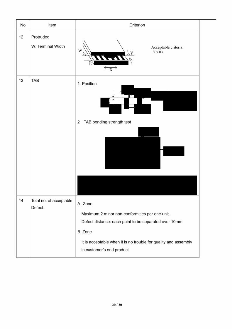
12 Protruded
W: Terminal Width
13 TAB1. Position
2 TAB bonding strength test
14 Total no. of acceptable
DefectA. Zone
Maximum 2 minor non-conformities per one unit.
Defect distance: each point to be separated over 10mm
B. Zone
It is acceptable when it is no trouble for quality and assembly
in customer’s end product.
W Y
X
Acceptable criteria: Y ≤ 0.4
ITO
TAB
W1W
H1H
W11/3W H11/3H
F
TAB
P (=F/TAB bonding width) 650gf/cm ,(speed rate: 1mm/min) 5pcs per SOA (shipment)

21 / 21
13.3 Reliability of LCM Reliability test condition:
Item Condition Time (hrs) Assessment
High temp. Storage 80°C 48
High temp. Operating 70°C 48
Low temp. Storage -30°C 48
Low temp. Operating -20°C 48
Humidity 40°C/ 90%RH 48
Temp. Cycle 0°C ← 25°C → 50°C
(30 min ← 5 min → 30min)10cycles
No abnormalities
in functions
and appearance
Recovery time should be 24 hours minimum. Moreover, functions, performance and appearance shall be free
from remarkable deterioration within 50,000 hours under ordinary operating and storage conditions room
temperature (20+8°C), normal humidity (below 65% RH), and in the area not exposed to direct sun light.
13.4 Precaution for using LCD/LCM LCD/LCM is assembled and adjusted with a high degree of precision. Do not attempt to make
any alteration or modification. The followings should be noted.
General Precautions:1. LCD panel is made of glass. Avoid excessive mechanical shock or applying strong
pressure onto the surface of display area.2. The polarizer used on the display surface is easily scratched and damaged. Extreme care
should be taken when handling. To clean dust or dirt off the display surface, wipe gently with cotton, or other soft material soaked with isoproply alcohol, ethyl alcohol or trichlorotriflorothane, do not use water, ketone or aromatics and never scrub hard.
3. Do not tamper in any way with the tabs on the metal frame.
4. Do not make any modification on the PCB without consulting AMOTEC
5. When mounting a LCM, make sure that the PCB is not under any stress such as bending
or twisting. Elastomer contacts are very delicate and missing pixels could result from
slight dislocation of any of the elements.
6. Avoid pressing on the metal bezel, otherwise the elastomer connector could be deformed
and lose contact, resulting in missing pixels and also cause rainbow on the display.7. Be careful not to touch or swallow liquid crystal that might leak from a damaged cell. Any liquid crystal
adheres to skin or clothes, wash it off immediately with soap and water.
Static Electricity Precautions:1. CMOS- LSI is used for the module circuit; therefore operators should be grounded whenever
he/she comes into contact with the module. 2. Do not touch any of the conductive parts such as the LSI pads; the copper leads on the PCB and
the interface terminals with any parts of the human body.

22 / 22
3. Do not touch the connection terminals of the display with bare hand; it will cause disconnection or defective insulation of terminals.
4. The modules should be kept in anti-static bags or other containers resistant to static for storage.5. Only properly grounded soldering irons should be used.6. If an electric screwdriver is used, it should be grounded and shielded to prevent sparks.7. The normal static prevention measures should be observed for work clothes and working
benches. 8. Since dry air is inductive to static, a relative humidity of 50-60% is recommended.
Soldering Precautions: 1. Soldering should be performed only on the I/O terminals.2. Use soldering irons with proper grounding and no leakage.3. Soldering temperature: 280°C+10°C4. Soldering time: 3 to 4 second.5. Use eutectic solder with resin flux filling.6. If flux is used, the LCD surface should be protected to avoid spattering flux.7. Flux residue should be removed.
Operation Precautions:1. The viewing angle can be adjusted by varying the LCD driving voltage Vo.2. Since applied DC voltage causes electro-chemical reactions, which deteriorate the display, the applied pulse waveform should be a symmetric waveform such that no DC component remains. Be sure to use the specified operating voltage.
3. Driving voltage should be kept within specified range; excess voltage will shorten display life.4. Response time increases with decrease in temperature.5. Display color may be affected at temperatures above its operational range.6.Keep the temperature within the specified range usage and storage. Excessive temperature and humidity could cause polarization degradation, polarizer peel-off or generate bubbles.
7. For long-term storage over 40 C is required, the relative humidity should be kept below 60%,and avoid
direct sunlight.Limited WarrantyAMOTEC LCDs and modules are not consumer products, but may be incorporated by AMOTEC ’s customers into consumer products or components thereof, AMOTEC does not warrant that its LCDs and components are fit for any such particular purpose.
1. The liability of AMOTEC is limited to repair or replacement on the terms set forth below. AMOTEC will not be responsible for any subsequent or consequential events or injury or damage to any personnel or user including third party personnel and/or user. Unless otherwise agreed in writing between AMOTEC and the customer, AMOTEC will only replace or repair any of its LCD which is found defective electrically or visually when inspected in accordance with AMOTEC general LCD inspection standard . (Copies available on request)
2. No warranty can be granted if any of the precautions state in handling liquid crystal display above has been disregarded. Broken glass, scratches on polarizer mechanical damages as well as defects that are caused accelerated environment tests are excluded from warranty.
3. In returning the LCD/LCM, they must be properly packaged; there should be detailed description of the failures or defect.

Appendix D
LM2678

Product
Folder
Order
Now
Technical
Documents
Tools &
Software
Support &Community
An IMPORTANT NOTICE at the end of this data sheet addresses availability, warranty, changes, use in safety-critical applications,intellectual property matters and other important disclaimers. PRODUCTION DATA.
LM2678SNVS029K –MARCH 2000–REVISED FEBRUARY 2017
LM2678 SIMPLE SWITCHER® High Efficiency 5-A Step-Down Voltage Regulator
1
1 Features1• Efficiency Up to 92%• Simple and Easy to Design Using Off-the-Shelf
External Components• 120-mΩ DMOS Output Switch• 3.3-V, 5-V, and 12-V Fixed Output and Adjustable
(1.2 V to 37 V) Versions• 50-μA Standby Current When Switched OFF• ±2% Maximum Output Tolerance Over Full Line
and Load Conditions• Wide Input Voltage Range: 8 V to 40 V• 260-kHz Fixed Frequency Internal Oscillator• −40 to 125°C Operating Junction Temperature
Range• Create a Custom Design Using the LM2678 With
the WEBENCH® Power Designer
2 Applications• Simple-to-Design, High Efficiency (>90%) Step-
Down Switching Regulators• Efficient System Preregulator for Linear Voltage
Regulators• Battery Chargers
3 DescriptionThe LM2678 series of regulators are monolithicintegrated circuits which provide all of the activefunctions for a step-down (buck) switching regulatorcapable of driving up to 5-A loads with excellent lineand load regulation characteristics. High efficiency(>90%) is obtained through the use of a low ON-resistance DMOS power switch. The series consistsof fixed output voltages of 3.3 V, 5 V, and 12 V andan adjustable output version.
The SIMPLE SWITCHER® concept provides for acomplete design using a minimum number of externalcomponents. A high fixed frequency oscillator(260 kHz) allows the use of physically smaller sizedcomponents. A family of standard inductors for usewith the LM2678 are available from severalmanufacturers to greatly simplify the design process.
The LM2678 series also has built-in thermalshutdown, current limiting, and an ON/OFF controlinput that can power down the regulator to a low 50-μA quiescent current standby condition. The outputvoltage is ensured to a ±2% tolerance. The clockfrequency is controlled to within a ±11% tolerance.
Device Information(1)
PART NUMBER PACKAGE BODY SIZE (NOM)
LM2678TO-263 (7) 10.10 mm × 8.89 mmTO-220 (7) 14.986 mm × 10.16 mmVSON (14) 6.00 mm × 5.00 mm
(1) For all available packages, see the orderable addendum atthe end of the data sheet.
Typical Application

2
LM2678SNVS029K –MARCH 2000–REVISED FEBRUARY 2017 www.ti.com
Product Folder Links: LM2678
Submit Documentation Feedback Copyright © 2000–2017, Texas Instruments Incorporated
Table of Contents1 Features .................................................................. 12 Applications ........................................................... 13 Description ............................................................. 14 Revision History..................................................... 25 Pin Configuration and Functions ......................... 36 Specifications......................................................... 4
6.1 Absolute Maximum Ratings ...................................... 46.2 ESD Ratings.............................................................. 46.3 Recommended Operating Conditions....................... 46.4 Thermal Information .................................................. 56.5 Electrical Characteristics – 3.3 V .............................. 56.6 Electrical Characteristics – 5 V ................................. 56.7 Electrical Characteristics – 12 V ............................... 66.8 Electrical Characteristics – Adjustable...................... 66.9 Electrical Characteristics – All Output Voltage
Versions ..................................................................... 66.10 Typical Characteristics ............................................ 7
7 Detailed Description ............................................ 107.1 Overview ................................................................. 107.2 Functional Block Diagram ....................................... 10
7.3 Feature Description................................................. 107.4 Device Functional Modes........................................ 11
8 Application and Implementation ........................ 128.1 Application Information............................................ 128.2 Typical Application .................................................. 14
9 Power Supply Recommendations ...................... 2610 Layout................................................................... 26
10.1 Layout Guidelines ................................................. 2610.2 Layout Example .................................................... 27
11 Device and Documentation Support ................. 2811.1 Custom Design With WEBENCH® Tools ............. 2811.2 Related Documentation......................................... 2811.3 Receiving Notification of Documentation Updates 2811.4 Community Resources.......................................... 2811.5 Trademarks ........................................................... 2811.6 Electrostatic Discharge Caution............................ 2811.7 Glossary ................................................................ 28
12 Mechanical, Packaging, and OrderableInformation ........................................................... 2912.1 VSON Package Devices ....................................... 29
4 Revision HistoryNOTE: Page numbers for previous revisions may differ from page numbers in the current version.
Changes from Revision J (June 2016) to Revision K Page
• Deleted RADJ = 5.6 kΩ .......................................................................................................................................................... 6• Deleted and updated with new values for Min, Typ and Max ............................................................................................... 6• Deleted and updated with new values for Min and Max ....................................................................................................... 6• Changed soft-start pin to ON/OFF pin.................................................................................................................................... 6• Changed to 200 µA from 1.5 mA............................................................................................................................................ 6• Changed typ and max values to 16 and 15 mA ..................................................................................................................... 6
Changes from Revision I (April 2013) to Revision J Page
• Added ESD Ratings table, Feature Description section, Device Functional Modes, Application and Implementationsection, Power Supply Recommendations section, Layout section, Device and Documentation Support section, andMechanical, Packaging, and Orderable Information section. ................................................................................................. 1
• Removed all references to Computer Design Software LM267X Made Simple (Version 6.0).............................................. 1
Changes from Revision H (April 2013) to Revision I Page
• Changed layout of National Data Sheet to TI format ........................................................................................................... 29

Not to scale
DAP
1NC 14 Switch_output
2Input 13 Switch_output
3Input 12 Switch_output
4CB 11 NC
5NC 10 NC
6NC 9 GND
7FB 8 ON/OFF
Not to scale
1S
witch
_o
utp
ut
2In
pu
t
3C
B
4G
ND
5N
C
6F
B
7O
N/O
FF
1 Switch_output
2 Input
3 CB
4 GND
5 NC
6 FB
7 ON/OFF
Not to scale
3
LM2678www.ti.com SNVS029K –MARCH 2000–REVISED FEBRUARY 2017
Product Folder Links: LM2678
Submit Documentation FeedbackCopyright © 2000–2017, Texas Instruments Incorporated
5 Pin Configuration and Functions
KTW Package7-Pin TO-263
Top ViewNDZ Package7-Pin TO-220
Top View
NHM Package14-Pin VSON
Top View
DAP connect to pin 9
Pin FunctionsPIN
I/O DESCRIPTIONNAME TO-263, TO-220 VSON
Switch output 1 12, 13, 14 O Source pin of the internal high-side FET. This is a switching node. Attachedthis pin to an inductor and the cathode of the external diode.
Input 2 2, 3 ISupply input pin to collector pin of high-side FET. Connect to power supplyand input bypass capacitors CIN. Path from VIN pin to high frequency bypassCIN and GND must be as short as possible.
CB 3 4 I Boot-strap capacitor connection for high-side driver. Connect a high-quality100-nF capacitor from CB to VSW Pin.
GND 4 9 — Power ground pins. Connect to system ground. Ground pins of CIN andCOUT. Path to CIN must be as short as possible.
FB 6 7 IFeedback sense input pin. Connect to the midpoint of feedback divider to setVOUT for ADJ version or connect this pin directly to the output capacitor for afixed output version.
ON/OFF 7 8 I Enable input to the voltage regulator. High = ON and low = OFF. Pull this pinhigh or float to enable the regulator.
NC 5 1, 5, 6, 10, 11 — No connect pins.

4
LM2678SNVS029K –MARCH 2000–REVISED FEBRUARY 2017 www.ti.com
Product Folder Links: LM2678
Submit Documentation Feedback Copyright © 2000–2017, Texas Instruments Incorporated
(1) Stresses beyond those listed under Absolute Maximum Ratings may cause permanent damage to the device. These are stress ratingsonly, which do not imply functional operation of the device at these or any other conditions beyond those indicated under RecommendedOperating Conditions. Exposure to absolute-maximum-rated conditions for extended periods may affect device reliability.
(2) If Military/Aerospace specified devices are required, please contact the Texas Instruments Sales Office/Distributors for availability andspecifications.
(3) The absolute maximum specification of the Switch Voltage to Ground applies to DC voltage. An extended negative voltage limit of –10 Vapplies to a pulse of up to 20 ns, –6 V of 60 ns and –3 V of up to 100 ns.
6 Specifications
6.1 Absolute Maximum Ratingsover operating free-air temperature range (unless otherwise noted) (1) (2)
MIN MAX UNITInput supply voltage 45 VSoft-start pin voltage –0.1 6 VSwitch voltage to ground (3) –1 VIN VBoost pin voltage VSW + 8 VFeedback pin voltage –0.3 14 VPower dissipation Internally limited
Soldering temperatureWave (4 s) 260
°CInfrared (10 s) 240Vapor phase (75 s) 219
Storage temperature, Tstg –65 150 °C
(1) JEDEC document JEP155 states that 500-V HBM allows safe manufacturing with a standard ESD control process.(2) ESD was applied using the human-body model, a 100-pF capacitor discharged through a 1.5-kΩ resistor into each pin.
6.2 ESD RatingsVALUE UNIT
V(ESD) Electrostatic discharge Human-body model (HBM), per ANSI/ESDA/JEDEC JS-001 (1) (2) ±2000 V
6.3 Recommended Operating ConditionsMIN MAX UNIT
Supply voltage 8 40 VJunction temperature, TJ –40 125 °C

5
LM2678www.ti.com SNVS029K –MARCH 2000–REVISED FEBRUARY 2017
Product Folder Links: LM2678
Submit Documentation FeedbackCopyright © 2000–2017, Texas Instruments Incorporated
(1) For more information about traditional and new thermal metrics, see the Semiconductor and IC Package Thermal Metrics applicationreport.
(2) Junction to ambient thermal resistance (no external heat sink) for the 7-lead TO-220 package mounted vertically, with ½ inch leads in asocket, or on a PCB with minimum copper area.
(3) Junction to ambient thermal resistance (no external heat sink) for the 7-lead TO-220 package mounted vertically, with ½ inch leadssoldered to a PCB containing approximately 4 square inches of (1 oz.) copper area surrounding the leads.
(4) Junction to ambient thermal resistance for the 7-lead DDPAK mounted horizontally against a PCB area of 0.136 square inches (thesame size as the DDPAK package) of 1 oz. (0.0014 in. thick) copper.
(5) Junction to ambient thermal resistance for the 7-lead DDPAK mounted horizontally against a PCB area of 0.4896 square inches (3.6times the area of the DDPAK package) of 1 oz. (0.0014 in. thick) copper.
(6) Junction to ambient thermal resistance for the 7-lead DDPAK mounted horizontally against a PCB copper area of 1.0064 square inches(7.4 times the area of the DDPAK 3 package) of 1 oz. (0.0014 in. thick) copper. Additional copper area reduces thermal resistancefurther.
(7) Junction to ambient thermal resistance for the 14-lead VSON mounted on a PCB copper area equal to the die attach paddle.(8) Junction to ambient thermal resistance for the 14-lead VSON mounted on a PCB copper area using 12 vias to a second layer of copper
equal to die attach paddle. Additional copper area will reduce thermal resistance further. For layout recommendations, see AN-1187Leadless Leadfram Package (LLP).
6.4 Thermal Information
THERMAL METRIC (1)LM2678
UNITNDZ (TO-220) KTW (TO-263) NHM (VSON)7 PINS 7 PINS 14 PINS
RθJA Junction-to-ambient thermal resistance
See (2) 65 — —
°C/W
See (3) 45 — —See (4) — 56 —See (5) — 35 —See (6) — 26 —See (7) — — 55See (8) — — 29
RθJC(top) Junction-to-case (top) thermal resistance 2 2 — °C/W
(1) All room temperature limits are 100% tested during production with TA = TJ = 25°C. All limits at temperature extremes are specifiedthrough correlation using standard Quality Control (SQC) methods. All limits are used to calculate Average Outgoing Quality Level(AOQL).
(2) Typical values are determined with TA = TJ = 25°C and represent the most likely norm.
6.5 Electrical Characteristics – 3.3 VSpecifications apply for TA = TJ = 25°C and RADJ = 5.6 kΩ (unless otherwise noted).
PARAMETER TEST CONDITIONS MIN (1) TYP (2) MAX (1) UNIT
VOUT Output voltage VIN = 8 V to 40 V,100 mA ≤ IOUT ≤ 5 A
TJ = 25°C 3.234 3.3 3.366V
TJ = –40°C to 125°C 3.201 3.399η Efficiency VIN = 12 V, ILOAD = 5 A 82%
(1) All room temperature limits are 100% tested during production with TA = TJ = 25°C. All limits at temperature extremes are specifiedthrough correlation using standard Quality Control (SQC) methods. All limits are used to calculate Average Outgoing Quality Level(AOQL).
(2) Typical values are determined with TA = TJ = 25°C and represent the most likely norm.
6.6 Electrical Characteristics – 5 VSpecifications apply for TA = TJ = 25°C and RADJ = 5.6 kΩ (unless otherwise noted).
PARAMETER TEST CONDITIONS MIN (1) TYP (2) MAX (1) UNIT
VOUT Output voltage VIN = 8 V to 40 V,100 mA ≤ IOUT ≤ 5 A
TJ = 25°C 4.9 5 5.1V
TJ = –40°C to 125°C 4.85 5.15η Efficiency VIN = 12 V, ILOAD = 5 A 84%

6
LM2678SNVS029K –MARCH 2000–REVISED FEBRUARY 2017 www.ti.com
Product Folder Links: LM2678
Submit Documentation Feedback Copyright © 2000–2017, Texas Instruments Incorporated
(1) All room temperature limits are 100% tested during production with TA = TJ = 25°C. All limits at temperature extremes are specifiedthrough correlation using standard Quality Control (SQC) methods. All limits are used to calculate Average Outgoing Quality Level(AOQL).
(2) Typical values are determined with TA = TJ = 25°C and represent the most likely norm.
6.7 Electrical Characteristics – 12 VSpecifications apply for TA = TJ = 25°C and RADJ = 5.6 kΩ (unless otherwise noted).
PARAMETER TEST CONDITIONS MIN (1) TYP (2) MAX (1) UNIT
VOUT Output voltage VIN = 15 V to 40 V,100 mA ≤ IOUT ≤ 5 A
TJ = 25°C 11.76 12 12.24V
TJ = –40°C to 125°C 11.64 12.36
η Efficiency VIN = 24 V, ILOAD = 5 A 92%
(1) All room temperature limits are 100% tested during production with TA = TJ = 25°C. All limits at temperature extremes are specifiedthrough correlation using standard Quality Control (SQC) methods. All limits are used to calculate Average Outgoing Quality Level(AOQL).
(2) Typical values are determined with TA = TJ = 25°C and represent the most likely norm.
6.8 Electrical Characteristics – AdjustableSpecifications apply for TA = TJ = 25°C and RADJ = 5.6 kΩ (unless otherwise noted).
PARAMETER TEST CONDITIONS MIN (1) TYP (2) MAX (1) UNIT
VFB Feedback voltageVIN = 8 V to 40 V,100 mA ≤ IOUT ≤ 5 AVOUT programmed for 5 V
TJ = 25°C 1.186 1.21 1.234V
TJ = –40°C to 125°C 1.174 1.246
η Efficiency VIN = 12 V, ILOAD = 5 A 84%
6.9 Electrical Characteristics – All Output Voltage VersionsSpecifications are for TA = TJ = 25°C, VIN = 12 V for the 3.3-V, 5-V, and adjustable versions, and VIN = 24 V for the 12-Vversion (unless otherwise noted).
PARAMETER TEST CONDITIONS MIN TYP MAX UNIT
IQ Quiescent current VFEEDBACK = 8 V for 3.3-V, 5-V, and adjustable versions,VFEEDBACK = 15 V for 12-V version 4.2 6 mA
ISTBY Standby quiescent current ON/OFF pin = 0 VTJ = 25°C 50 100
µATJ = –40°C to 125°C 150
ICL Current limitTJ = 25°C 6.1 7 8.3
ATJ = –40°C to 125°C 5.75 8.75
IL Output leakage current VIN = 40 V, ON/OFF pin = 0 VVSWITCH = 0 V 200 µA
VSWITCH = –1 V 16 15 mA
RDS(ON) Switch ON-Resistance ISWITCH = 5 ATJ = 25°C 0.12 0.14
ΩTJ = –40°C to 125°C 0.225
fO Oscillator frequency Measured at switch pinTJ = 25°C 260
kHzTJ = –40°C to 125°C 225 280
D Duty cycleMaximum duty cycle 91%
Minimum duty cycle 0%
IBIASFeedback biascurrent VFEEDBACK = 1.3 V (adjustable version only) 85 nA
VON/OFF ON/OFF threshold voltageTJ = 25°C 1.4
VTJ = –40°C to 125°C 0.8 2
ION/OFF ON/OFF input current ON/OFF input = 0 VTJ = 25°C 20
μATJ = –40°C to 125°C 45

7
LM2678www.ti.com SNVS029K –MARCH 2000–REVISED FEBRUARY 2017
Product Folder Links: LM2678
Submit Documentation FeedbackCopyright © 2000–2017, Texas Instruments Incorporated
6.10 Typical Characteristics
Figure 1. Normalized Output Voltage Figure 2. Line Regulation
Figure 3. Efficiency vs Input Voltage Figure 4. Efficiency vs ILOAD
Figure 5. Switch Current Limit Figure 6. Operating Quiescent Current

8
LM2678SNVS029K –MARCH 2000–REVISED FEBRUARY 2017 www.ti.com
Product Folder Links: LM2678
Submit Documentation Feedback Copyright © 2000–2017, Texas Instruments Incorporated
Typical Characteristics (continued)
Figure 7. Standby Quiescent Current Figure 8. ON/OFF Threshold Voltage
Figure 9. ON/OFF Pin Current (Sourcing) Figure 10. Switching Frequency
Figure 11. Feedback Pin Bias Current
Continuous Mode Switching Waveforms, VIN = 20 V, VOUT = 5 V,ILOAD = 5 A, L = 10 μH, COUT = 400 μF, COUTESR = 13 mΩA. VSW pin voltage = 10 V/divB. Inductor current = 2 A/divC. Output ripple voltage = 20 mV/div AC-coupled
Figure 12. Horizontal Time Base: 1 μs/div

9
LM2678www.ti.com SNVS029K –MARCH 2000–REVISED FEBRUARY 2017
Product Folder Links: LM2678
Submit Documentation FeedbackCopyright © 2000–2017, Texas Instruments Incorporated
Typical Characteristics (continued)
Discontinuous Mode Switching Waveforms, VIN = 20 V,VOUT = 5 V, ILOAD = 500 mA, L = 10 μH, COUT = 400 μF,COUTESR = 13 mΩA. VSW pin voltage = 10 V/divB. Inductor current = 1 A/divC. Output ripple voltage = 20 mV/div AC-coupled
Figure 13. Horizontal Time Base: 1 μs/div
Load Transient Response for Continuous Mode, VIN = 20 V,VOUT = 5 V, L = 10 μH, COUT = 400 μF,COUTESR = 13 mΩA. Output voltage = 100 mV/div, AC-coupledB. Load current = 500-mA to 5-A load pulse
Figure 14. Horizontal Time Base: 100 μs/div
Load Transient Response for Discontinuous Mode, VIN = 20 V, VOUT = 5 V, vs L = 10 μH, COUT = 400 μF, COUTESR = 13 mΩA. Output voltage = 100 mV/div, AC-coupledB. Load current = 200-mA to 3-A load pulse
Figure 15. Horizontal Time Base: 200 μs/div

10
LM2678SNVS029K –MARCH 2000–REVISED FEBRUARY 2017 www.ti.com
Product Folder Links: LM2678
Submit Documentation Feedback Copyright © 2000–2017, Texas Instruments Incorporated
7 Detailed Description
7.1 OverviewThe LM2678 provides all of the active functions required for a step-down (buck) switching regulator. The internalpower switch is a DMOS power MOSFET to provide power supply designs with high current capability, up to 5 A,and highly efficient operation.
The LM2678 is part of the SIMPLE SWITCHER® family of power converters. The design support WEBENCH,can also be used to provide instant component selection, circuit performance calculations for evaluation, a bill ofmaterials component list and a circuit schematic for LM2678.
7.2 Functional Block Diagram
7.3 Feature Description
7.3.1 Switch OutputThis is the output of a power MOSFET switch connected directly to the input voltage. The switch provides energyto an inductor, an output capacitor and the load circuitry under control of an internal pulse-width-modulator(PWM). The PWM controller is internally clocked by a fixed 260-kHz oscillator. In a standard step-downapplication the duty cycle (Time ON/Time OFF) of the power switch is proportional to the ratio of the powersupply output voltage to the input voltage. The voltage on pin 1 switches between Vin (switch ON) and belowground by the voltage drop of the external Schottky diode (switch OFF).

11
LM2678www.ti.com SNVS029K –MARCH 2000–REVISED FEBRUARY 2017
Product Folder Links: LM2678
Submit Documentation FeedbackCopyright © 2000–2017, Texas Instruments Incorporated
Feature Description (continued)7.3.2 InputThe input voltage for the power supply is connected to pin 2. In addition to providing energy to the load the inputvoltage also provides bias for the internal circuitry of the LM2678. For ensured performance the input voltagemust be in the range of 8 V to 40 V. For best performance of the power supply the input pin must always bebypassed with an input capacitor located close to pin 2.
7.3.3 C BoostA capacitor must be connected from pin 3 to the switch output, pin 1. This capacitor boosts the gate drive to theinternal MOSFET above VIN to fully turn it ON. This minimizes conduction losses in the power switch to maintainhigh efficiency. The recommended value for C Boost is 0.01 μF.
7.3.4 GroundThis is the ground reference connection for all components in the power supply. In fast-switching, high-currentapplications such as those implemented with the LM2678, TI recommends that a broad ground plane be used tominimize signal coupling throughout the circuit.
7.3.5 FeedbackThis is the input to a two-stage high gain amplifier, which drives the PWM controller. It is necessary to connectpin 6 to the actual output of the power supply to set the DC output voltage. For the fixed output devices (3.3-V, 5-V and 12-V outputs), a direct wire connection to the output is all that is required as internal gain setting resistorsare provided inside the LM2678. For the adjustable output version two external resistors are required to set theDC output voltage. For stable operation of the power supply it is important to prevent coupling of any inductorflux to the feedback input.
7.3.6 ON/OFFThis input provides an electrical ON/OFF control of the power supply. Connecting this pin to ground or to anyvoltage less than 0.8 V is completely turn OFF the regulator. The current drain from the input supply when OFFis only 50 μA. Pin 7 has an internal pullup current source of approximately 20 μA and a protection clamp Zenerdiode of 7 V to ground. When electrically driving the ON/OFF pin the high voltage level for the ON conditionshould not exceed the 6 V absolute maximum limit. When ON/OFF control is not required pin 7 should be leftopen circuited.
7.4 Device Functional Modes
7.4.1 Shutdown ModeThe ON/OFF pin provides electrical ON and OFF control for the LM2678. When the voltage of this pin is lowerthan 1.4 V, the device enters shutdown mode. The typical standby current in this mode is 45 μA.
7.4.2 Active ModeWhen the voltage of the ON/OFF pin is higher than 1.4 V, the device starts switching and the output voltage risesuntil it reaches a normal regulation voltage.

12
LM2678SNVS029K –MARCH 2000–REVISED FEBRUARY 2017 www.ti.com
Product Folder Links: LM2678
Submit Documentation Feedback Copyright © 2000–2017, Texas Instruments Incorporated
8 Application and Implementation
NOTEInformation in the following applications sections is not part of the TI componentspecification, and TI does not warrant its accuracy or completeness. TI’s customers areresponsible for determining suitability of components for their purposes. Customers shouldvalidate and test their design implementation to confirm system functionality.
8.1 Application Information
8.1.1 Design ConsiderationsPower supply design using the LM2678 is greatly simplified by using recommended external components. A widerange of inductors, capacitors, and Schottky diodes from several manufacturers have been evaluated for use indesigns that cover the full range of capabilities (input voltage, output voltage, and load current) of the LM2678. Asimple design procedure using nomographs and component tables provided in this data sheet leads to a workingdesign with very little effort.
The individual components from the various manufacturers called out for use are still just a small sample of thevast array of components available in the industry. While these components are recommended, they are notexclusively the only components for use in a design. After a close comparison of component specifications,equivalent devices from other manufacturers could be substituted for use in an application.
Important considerations for each external component and an explanation of how the nomographs and selectiontables were developed follows.
8.1.2 InductorThe inductor is the key component in a switching regulator. For efficiency the inductor stores energy during theswitch ON time and then transfers energy to the load while the switch is OFF.
Nomographs are used to select the inductance value required for a given set of operating conditions. Thenomographs assume that the circuit is operating in continuous mode (the current flowing through the inductornever falls to zero). The magnitude of inductance is selected to maintain a maximum ripple current of 30% of themaximum load current. If the ripple current exceeds this 30% limit the next larger value is selected.
The inductors offered have been specifically manufactured to provide proper operation under all operatingconditions of input and output voltage and load current. Several part types are offered for a given amount ofinductance. Both surface mount and through-hole devices are available. The inductors from each of the threemanufacturers have unique characteristics.• Renco: ferrite stick core inductors; benefits are typically lowest cost and can withstand ripple and transient
peak currents above the rated value. These inductors have an external magnetic field, which may generateEMI.
• Pulse Engineering: powdered iron toroid core inductors; these also can withstand higher than rated currentsand, being toroid inductors, have low EMI.
• Coilcraft: ferrite drum core inductors; these are the smallest physical size inductors and are available only assurface mount components. These inductors also generate EMI but less than stick inductors.
8.1.3 Output CapacitorThe output capacitor acts to smooth the DC output voltage and also provides energy storage. Selection of anoutput capacitor, with an associated equivalent series resistance (ESR), impacts both the amount of output ripplevoltage and stability of the control loop.
The output ripple voltage of the power supply is the product of the capacitor ESR and the inductor ripple current.The capacitor types recommended in the tables were selected for having low ESR ratings.
In addition, both surface mount tantalum capacitors and through-hole aluminum electrolytic capacitors are offeredas solutions.

13
LM2678www.ti.com SNVS029K –MARCH 2000–REVISED FEBRUARY 2017
Product Folder Links: LM2678
Submit Documentation FeedbackCopyright © 2000–2017, Texas Instruments Incorporated
Application Information (continued)Impacting frequency stability of the overall control loop, the output capacitance, in conjunction with the inductor,creates a double pole inside the feedback loop. In addition the capacitance and the ESR value create a zero.These frequency response effects together with the internal frequency compensation circuitry of the LM2678modify the gain and phase shift of the closed-loop system.
As a general rule for stable switching regulator circuits it is desired to have the unity gain bandwidth of the circuitto be limited to no more than one-sixth of the controller switching frequency. With the fixed 260-kHz switchingfrequency of the LM2678, the output capacitor is selected to provide a unity gain bandwidth of 40 kHz maximum.Each recommended capacitor value has been chosen to achieve this result.
In some cases multiple capacitors are required either to reduce the ESR of the output capacitor, to minimizeoutput ripple (a ripple voltage of 1% of VOUT or less is the assumed performance condition), or to increase theoutput capacitance to reduce the closed loop unity gain bandwidth (to less than 40 kHz). When parallelcombinations of capacitors are required it has been assumed that each capacitor is the exact same part type.
The RMS current and working voltage (WV) ratings of the output capacitor are also important considerations. In atypical step-down switching regulator, the inductor ripple current (set to be no more than 30% of the maximumload current by the inductor selection) is the current that flows through the output capacitor. The capacitor RMScurrent rating must be greater than this ripple current. The voltage rating of the output capacitor should begreater than 1.3 times the maximum output voltage of the power supply. If operation of the system at elevatedtemperatures is required, the capacitor voltage rating may be de-rated to less than the nominal room temperaturerating. Careful inspection of the manufacturer's specification for de-rating of working voltage with temperature isimportant.
8.1.4 Input CapacitorFast changing currents in high current switching regulators place a significant dynamic load on the unregulatedpower source. An input capacitor helps to provide additional current to the power supply as well as smooth outinput voltage variations.
Like the output capacitor, the key specifications for the input capacitor are RMS current rating and workingvoltage. The RMS current flowing through the input capacitor is equal to one-half of the maximum DC loadcurrent so the capacitor should be rated to handle this. Paralleling multiple capacitors proportionally increasesthe current rating of the total capacitance. The voltage rating should also be selected to be 1.3 times themaximum input voltage. Depending on the unregulated input power source, under light load conditions themaximum input voltage could be significantly higher than normal operation and should be considered whenselecting an input capacitor.
The input capacitor must be placed very close to the input pin of the LM2678. Due to relative high currentoperation with fast transient changes, the series inductance of input connecting wires or PCB traces can createringing signals at the input terminal which could possibly propagate to the output or other parts of the circuitry. Itmay be necessary in some designs to add a small valued (0.1 μF to 0.47 μF) ceramic type capacitor in parallelwith the input capacitor to prevent or minimize any ringing.
8.1.5 Catch DiodeWhen the power switch in the LM2678 turns OFF, the current through the inductor continues to flow. The path forthis current is through the diode connected between the switch output and ground. This forward biased diodeclamps the switch output to a voltage less than ground. This negative voltage must be greater than −1 V so a lowvoltage drop (particularly at high current levels) Schottky diode is recommended. Total efficiency of the entirepower supply is significantly impacted by the power lost in the output catch diode. The average current throughthe catch diode is dependent on the switch duty cycle (D) and is equal to the load current times (1-D). Use of adiode rated for much higher current than is required by the actual application helps to minimize the voltage dropand power loss in the diode.
During the switch ON time the diode will be reversed biased by the input voltage. The reverse voltage rating ofthe diode must be at least 1.3 times greater than the maximum input voltage.

14
LM2678SNVS029K –MARCH 2000–REVISED FEBRUARY 2017 www.ti.com
Product Folder Links: LM2678
Submit Documentation Feedback Copyright © 2000–2017, Texas Instruments Incorporated
Application Information (continued)8.1.6 Boost CapacitorThe boost capacitor creates a voltage used to overdrive the gate of the internal power MOSFET. This improvesefficiency by minimizing the ON-resistance of the switch and associated power loss. For all applications it isrecommended to use a 0.01-μF, 50-V ceramic capacitor.
8.1.7 Additional Application InformationWhen the output voltage is greater than approximately 6 V, and the duty cycle at minimum input voltage isgreater than approximately 50%, the designer should exercise caution in selection of the output filtercomponents. When an application designed to these specific operating conditions is subjected to a current limitfault condition, it may be possible to observe a large hysteresis in the current limit. This can affect the outputvoltage of the device until the load current is reduced sufficiently to allow the current limit protection circuit toreset itself.
Under current limiting conditions, the LM267x is designed to respond in the following manner:1. At the moment when the inductor current reaches the current limit threshold, the ON-pulse is immediately
terminated. This happens for any application condition.2. However, the current limit block is also designed to momentarily reduce the duty cycle to below 50% to avoid
subharmonic oscillations, which could cause the inductor to saturate.3. Thereafter, once the inductor current falls below the current limit threshold, there is a small relaxation time
during which the duty cycle progressively rises back above 50% to the value required to achieve regulation.
If the output capacitance is sufficiently large, it may be possible that as the output tries to recover, the outputcapacitor charging current is large enough to repeatedly re-trigger the current limit circuit before the output hasfully settled. This condition is exacerbated with higher output voltage settings because the energy requirement ofthe output capacitor varies as the square of the output voltage (½ CV2), thus requiring an increased chargingcurrent.
A simple test to determine if this condition might exist for a suspect application is to apply a short circuit acrossthe output of the converter, and then remove the shorted output condition. In an application with properlyselected external components, the output will recover smoothly.
Practical values of external components that have been experimentally found to work well under these specificoperating conditions are COUT = 47 µF, L = 22 µH. It should be noted that even with these components, for adevice’s current limit of ICLIM, the maximum load current under which the possibility of the large current limithysteresis can be minimized is ICLIM/2. For example, if the input is 24 V and the set output voltage is 18 V, thenfor a desired maximum current of 1.5 A, the current limit of the chosen switcher must be confirmed to be at least3 A.
Under extreme overcurrent or short circuit conditions, the LM267X employs frequency foldback in addition to thecurrent limit. If the cycle-by-cycle inductor current increases above the current limit threshold (due to short circuitor inductor saturation for example) the switching frequency is automatically reduced to protect the IC. Frequencybelow 100 kHz is typical for an extreme short-circuit condition.
8.2 Typical Application
8.2.1 All Output Voltage Versions
Figure 16. Typical Application for All Output Voltage Versions

15
LM2678www.ti.com SNVS029K –MARCH 2000–REVISED FEBRUARY 2017
Product Folder Links: LM2678
Submit Documentation FeedbackCopyright © 2000–2017, Texas Instruments Incorporated
Typical Application (continued)8.2.1.1 Design RequirementsSelect the power supply operating conditions and the maximum output current and follow below procedures tofind the external components for LM2678.
8.2.1.2 Detailed Design Procedure
8.2.1.2.1 Custom Design With WEBENCH® Tools
Click here to create a custom design using the LM2678 device with the WEBENCH® Power Designer.1. Start by entering the input voltage (VIN), output voltage (VOUT), and output current (IOUT) requirements.2. Optimize the design for key parameters such as efficiency, footprint, and cost using the optimizer dial.3. Compare the generated design with other possible solutions from Texas Instruments.
The WEBENCH Power Designer provides a customized schematic along with a list of materials with real-timepricing and component availability.
In most cases, these actions are available:• Run electrical simulations to see important waveforms and circuit performance• Run thermal simulations to understand board thermal performance• Export customized schematic and layout into popular CAD formats• Print PDF reports for the design, and share the design with colleagues
Get more information about WEBENCH tools at www.ti.com/WEBENCH.
Using the nomographs and tables in this data sheet (or use the available design software at www.ti.com) acomplete step-down regulator can be designed in a few simple steps.
Step 1: Define the power supply operating conditions:• Required output voltage• Maximum DC input voltage• Maximum output load current
Step 2: Set the output voltage by selecting a fixed output LM2678 (3.3-V, 5-V, or 12-V applications) or determinethe required feedback resistors for use with the adjustable LM2678−ADJ
Step 3: Determine the inductor required by using one of the four nomographs, Figure 17 through Figure 20.Table 3 provides a specific manufacturer and part number for the inductor.
Step 4: Using Table 5 (fixed output voltage) or Table 9 (adjustable output voltage), determine the outputcapacitance required for stable operation. Table 1 provides the specific capacitor type from the manufacturer ofchoice.
Step 5: Determine an input capacitor from Table 5 for fixed output voltage applications. Use Table 1 to find thespecific capacitor type. For adjustable output circuits select a capacitor from Table 1 with a sufficient workingvoltage (WV) rating greater than VIN max, and an RMS current rating greater than one-half the maximum loadcurrent (2 or more capacitors in parallel may be required).
Step 6: Select a diode from Table 4. The current rating of the diode must be greater than ILOAD max and thereverse voltage rating must be greater than VIN maximum.
Step 7: Include a 0.01-μF, 50-V capacitor for CBOOST in the design.
8.2.1.2.2 Capacitor Selection Guides
Table 1. Input and Output Capacitor Codes – Surface Mount
CAPACITORREFERENCE
CODE
SURFACE MOUNT
AVX TPS SERIES SPRAGUE 594D SERIES KEMET T495 SERIES
C (µF) WV (V) Irms (A) C (µF) WV (V) Irms (A) C (µF) WV (V) Irms (A)
C1 330 6.3 1.15 120 6.3 1.1 100 6.3 0.82
C2 100 10 1.1 220 6.3 1.4 220 6.3 1.1

16
LM2678SNVS029K –MARCH 2000–REVISED FEBRUARY 2017 www.ti.com
Product Folder Links: LM2678
Submit Documentation Feedback Copyright © 2000–2017, Texas Instruments Incorporated
Typical Application (continued)Table 1. Input and Output Capacitor Codes – Surface Mount (continued)
CAPACITORREFERENCE
CODE
SURFACE MOUNT
AVX TPS SERIES SPRAGUE 594D SERIES KEMET T495 SERIES
C (µF) WV (V) Irms (A) C (µF) WV (V) Irms (A) C (µF) WV (V) Irms (A)
C3 220 10 1.15 68 10 1.05 330 6.3 1.1
C4 47 16 0.89 150 10 1.35 100 10 1.1
C5 100 16 1.15 47 16 1 150 10 1.1
C6 33 20 0.77 100 16 1.3 220 10 1.1
C7 68 20 0.94 180 16 1.95 33 20 0.78
C8 22 25 0.77 47 20 1.15 47 20 0.94
C9 10 35 0.63 33 25 1.05 68 20 0.94
C10 22 35 0.66 68 25 1.6 10 35 0.63
C11 — — — 15 35 0.75 22 35 0.63
C12 — — — 33 35 1 4.7 50 0.66
C13 — — — 15 50 0.9 — — —

17
LM2678www.ti.com SNVS029K –MARCH 2000–REVISED FEBRUARY 2017
Product Folder Links: LM2678
Submit Documentation FeedbackCopyright © 2000–2017, Texas Instruments Incorporated
Table 2. Input and Output Capacitor Codes – Through Hole
CAPACITORREFERENCE
CODE
THROUGH HOLE
SANYO OS-CON SA SERIES SANYO MV-GX SERIES NICHICON PL SERIES PANASONIC HFQ SERIES
C (µF) WV (V) Irms (A) C (µF) WV (V) Irms (A) C (µF) WV (V) Irms (A) C (µF) WV (V) Irms (A)
C1 47 6.3 1 1000 6.3 0.8 680 10 0.8 82 35 0.4
C2 150 6.3 1.95 270 16 0.6 820 10 0.98 120 35 0.44
C3 330 6.3 2.45 470 16 0.75 1000 10 1.06 220 35 0.76
C4 100 10 1.87 560 16 0.95 1200 10 1.28 330 35 1.01
C5 220 10 2.36 820 16 1.25 2200 10 1.71 560 35 1.4
C6 33 16 0.96 1000 16 1.3 3300 10 2.18 820 35 1.62
C7 100 16 1.92 150 35 0.65 3900 10 2.36 1000 35 1.73
C8 150 16 2.28 470 35 1.3 6800 10 2.68 2200 35 2.8
C9 100 20 2.25 680 35 1.4 180 16 0.41 56 50 0.36
C10 47 25 2.09 1000 35 1.7 270 16 0.55 100 50 0.5
C11 — — — 220 63 0.76 470 16 0.77 220 50 0.92
C12 — — — 470 63 1.2 680 16 1.02 470 50 1.44
C13 — — — 680 63 1.5 820 16 1.22 560 50 1.68
C14 — — — 1000 63 1.75 1800 16 1.88 1200 50 2.22
C15 — — — — — — 220 25 0.63 330 63 1.42
C16 — — — — — — 220 35 0.79 1500 63 2.51
C17 — — — — — — 560 35 1.43 — — —
C18 — — — — — — 2200 35 2.68 — — —
C19 — — — — — — 150 50 0.82 — — —
C20 — — — — — — 220 50 1.04 — — —
C21 — — — — — — 330 50 1.3 — — —
C22 — — — — — — 100 63 0.75 — — —
C23 — — — — — — 390 63 1.62 — — —
C24 — — — — — — 820 63 2.22 — — —
C25 — — — — — — 1200 63 2.51 — — —
Table 3. Inductor Manufacturer Part Numbers
INDUCTORREFERENCE
NUMBERINDUCTANCE
(µH)CURRENT
(A)
RENCO PULSE ENGINEERING COILCRAFT
THROUGH HOLE SURFACEMOUNT THROUGH HOLE SURFACE
MOUNT SURFACE MOUNT
L23 33 1.35 RL-5471-7 RL1500-33 PE-53823 PE-53823S DO3316-333
L24 22 1.65 RL-1283-22-43 RL1500-22 PE-53824 PE-53824S DO3316-223
L25 15 2 RL-1283-15-43 RL1500-15 PE-53825 PE-53825S DO3316-153
L29 100 1.41 RL-5471-4 RL-6050-100 PE-53829 PE-53829S DO5022P-104
L30 68 1.71 RL-5471-5 RL6050-68 PE-53830 PE-53830S DO5022P-683
L31 47 2.06 RL-5471-6 RL6050-47 PE-53831 PE-53831S DO5022P-473
L32 33 2.46 RL-5471-7 RL6050-33 PE-53932 PE-53932S DO5022P-333
L33 22 3.02 RL-1283-22-43 RL6050-22 PE-53933 PE-53933S DO5022P-223
L34 15 3.65 RL-1283-15-43 — PE-53934 PE-53934S DO5022P-153
L38 68 2.97 RL-5472-2 — PE-54038 PE-54038S —
L39 47 3.57 RL-5472-3 — PE-54039 PE-54039S —
L40 33 4.26 RL-1283-33-43 — PE-54040 PE-54040S —
L41 22 5.22 RL-1283-22-43 — PE-54041 P0841 —
L44 68 3.45 RL-5473-3 — PE-54044 — —
L45 10 4.47 RL-1283-10-43 — — P0845 DO5022P-103HC
L46 15 5.6 RL-1283-15-43 — — P0846 DO5022P-153HC
L47 10 5.66 RL-1283-10-43 — — P0847 DO5022P-103HC
L48 47 5.61 RL-1282-47-43 — — P0848 —
L49 33 5.61 RL-1282-33-43 — — P0849 —

18
LM2678SNVS029K –MARCH 2000–REVISED FEBRUARY 2017 www.ti.com
Product Folder Links: LM2678
Submit Documentation Feedback Copyright © 2000–2017, Texas Instruments Incorporated
Table 4. Schottky Diode Selection Table
REVERSE VOLTAGE (V)SURFACE MOUNT THROUGH HOLE
3 A 5 A OR MORE 3 A 5 A OR MORE
20 SK32 —1N5820
—SR302
30SK33
MBRD835L1N5821
—30WQ03F 31DQ03
40
SK34 MBRD1545CT 1N5822 1N582530BQ040 6TQ045S MBR340 MBR74530WQ04F — 31DQ04 80SQ045MBRS340 — SR403 6TQ045MBRD340 — — —
50 or moreSK35 — MBR350 —
30WQ05F — 31DQ05 —— — SR305 —
8.2.1.3 Application CurvesFor continuous mode operation
Figure 17. LM2678-3.3 Figure 18. LM2678-5
Figure 19. LM2678-12 Figure 20. LM2678-Adjustable

19
LM2678www.ti.com SNVS029K –MARCH 2000–REVISED FEBRUARY 2017
Product Folder Links: LM2678
Submit Documentation FeedbackCopyright © 2000–2017, Texas Instruments Incorporated
8.2.2 Fixed Output Voltage Design Example
Figure 21. Basic Circuit for Fixed Output Voltage Applications
8.2.2.1 Detailed Design ProcedureA system logic power supply bus of 3.3 V is to be generated from a wall adapter which provides an unregulatedDC voltage of 13 V to 16 V. The maximum load current is 4 A. Through-hole components are preferred.
Step 1: Operating conditions are:• VOUT = 3.3 V• VIN max = 16 V• ILOAD max = 4 A
Step 2: Select a LM2678 3.3-V. The output voltage has a tolerance of ±2% at room temperature and ±3% overthe full operating temperature range.
Step 3: Use the nomograph for the 3.3-V device, Figure 17. The intersection of the 16-V horizontal line (Vin max)and the 4-A vertical line (Iload max) indicates that L46, a 15-μH inductor, is required.
From Table 3, L46 in a through-hole component is available from Renco with part number RL-1283-15-43.
Step 4: Use Table 5 to determine an output capacitor. With a 3.3-V output and a 15-μH inductor there are fourthrough-hole output capacitor solutions with the number of same type capacitors to be paralleled and anidentifying capacitor code given. Table 1 provides the actual capacitor characteristics. Any of the followingchoices work in the circuit:• 2 × 220-μF, 10-V Sanyo OS-CON (code C5)• 2 × 820-μF, 16-V Sanyo MV-GX (code C5)• 1 × 3900-μF, 10-V Nichicon PL (code C7)• 2 × 560-μF, 35-V Panasonic HFQ (code C5)
Step 5: Use Table 5 to select an input capacitor. With 3.3-V output and 15 μH there are three through-holesolutions. These capacitors provide a sufficient voltage rating and an RMS current rating greater than 2 A (1/2Iload max). Again using Table 1 for specific component characteristics the following choices are suitable:• 2 × 680-μF, 63-V Sanyo MV-GX (code C13)• 1 × 1200-μF, 63-V Nichicon PL (code C25)• 1 × 1500-μF, 63-V Panasonic HFQ (code C16)
Step 6: From Table 4 a 5-A or more Schottky diode must be selected. For through-hole components only 40-Vrated diodes are indicated and 4 part types are suitable:• 1N5825• MBR745• 80SQ045• 6TQ045
Step 7: A 0.01-μF capacitor is used for CBOOST.
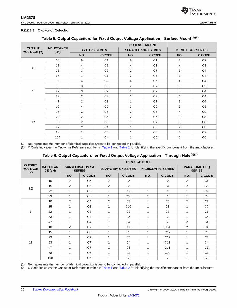
20
LM2678SNVS029K –MARCH 2000–REVISED FEBRUARY 2017 www.ti.com
Product Folder Links: LM2678
Submit Documentation Feedback Copyright © 2000–2017, Texas Instruments Incorporated
(1) No. represents the number of identical capacitor types to be connected in parallel.(2) C Code indicates the Capacitor Reference number in Table 1 and Table 2 for identifying the specific component from the manufacturer.
8.2.2.1.1 Capacitor Selection
Table 5. Output Capacitors for Fixed Output Voltage Application—Surface Mount (1) (2)
OUTPUTVOLTAGE (V)
INDUCTANCE(µH)
SURFACE MOUNTAVX TPS SERIES SPRAGUE 594D SERIES KEMET T495 SERIES
NO. C CODE NO. C CODE NO. C CODE
3.3
10 5 C1 5 C1 5 C215 4 C1 4 C1 4 C322 3 C2 2 C7 3 C433 1 C1 2 C7 3 C4
5
10 4 C2 4 C6 4 C415 3 C3 2 C7 3 C522 3 C2 2 C7 3 C433 2 C2 2 C3 2 C447 2 C2 1 C7 2 C4
12
10 4 C5 3 C6 5 C915 3 C5 2 C7 4 C922 2 C5 2 C6 3 C833 2 C5 1 C7 3 C847 2 C4 1 C6 2 C868 1 C5 1 C5 2 C7100 1 C4 1 C5 1 C8
(1) No. represents the number of identical capacitor types to be connected in parallel.(2) C Code indicates the Capacitor Reference number in Table 1 and Table 2 for identifying the specific component from the manufacturer.
Table 6. Output Capacitors for Fixed Output Voltage Application—Through Hole (1) (2)
OUTPUTVOLTAGE
(V)INDUCTAN
CE (µH)
THROUGH HOLESANYO OS-CON SA
SERIES SANYO MV-GX SERIES NICHICON PL SERIES PANASONIC HFQSERIES
NO. C CODE NO. C CODE NO. C CODE NO. C CODE
3.3
10 2 C5 2 C6 1 C8 2 C615 2 C5 2 C5 1 C7 2 C522 1 C5 1 C10 1 C5 1 C733 1 C5 1 C10 1 C5 1 C7
5
10 2 C4 2 C5 1 C6 2 C515 1 C5 1 C10 1 C5 1 C722 1 C5 1 C9 1 C5 1 C533 1 C4 1 C5 1 C4 1 C447 1 C4 1 C4 1 C2 2 C4
12
10 2 C7 1 C10 1 C14 2 C415 1 C8 1 C6 1 C17 1 C522 1 C7 1 C5 1 C13 1 C533 1 C7 1 C4 1 C12 1 C447 1 C7 1 C3 1 C11 1 C368 1 C6 1 C2 1 C10 1 C3100 1 C6 1 C2 1 C9 1 C1

21
LM2678www.ti.com SNVS029K –MARCH 2000–REVISED FEBRUARY 2017
Product Folder Links: LM2678
Submit Documentation FeedbackCopyright © 2000–2017, Texas Instruments Incorporated
(1) No. represents the number of identical capacitor types to be connected in parallel.(2) C Code indicates the Capacitor Reference number in Table 1 and Table 2 for identifying the specific component from the manufacturer.(3) Assumes worst case maximum input voltage and load current for a given inductance value.(4) Check voltage rating of capacitors to be greater than application input voltage.
Table 7. Input Capacitors for Fixed Output Voltage Application—Surface Mount (1) (2) (3)
OUTPUTVOLTAGE (V)
INDUCTANCE(µH)
SURFACE MOUNTAVX TPS SERIES SPRAGUE 594D SERIES KEMET T495 SERIES
NO. C CODE NO. C CODE NO. C CODE
3.3
10 3 C7 2 C10 3 C915 See (4) See (4) 3 C13 4 C1222 See (4) See (4) 2 C13 3 C1233 See (4) See (4) 2 C13 3 C12
5
10 3 C4 2 C6 3 C915 4 C9 3 C12 4 C1022 See (4) See (4) 3 C13 4 C1233 See (4) See (4) 2 C13 3 C1247 See (4) See (4) 1 C13 2 C12
12
10 4 C9 2 C10 4 C1015 4 C8 2 C10 4 C1022 4 C9 3 C12 4 C1033 See (4) See (4) 3 C13 4 C1247 See (4) See (4) 2 C13 3 C1268 See (4) See (4) 2 C13 2 C12100 See (4) See (4) 1 C13 2 C12
(1) No. represents the number of identical capacitor types to be connected in parallel.(2) C Code indicates the Capacitor Reference number in Table 1 and Table 2 for identifying the specific component from the manufacturer.(3) Assumes worst case maximum input voltage and load current for a given inductance value.(4) Check voltage rating of capacitors to be greater than application input voltage.
Table 8. Input Capacitors for Fixed Output Voltage Application—Through Hole (1) (2) (3)
OUTPUTVOLTAGE
(V)INDUCTAN
CE (µH)
THROUGH HOLESANYO OS-CON SA
SERIES SANYO MV-GX SERIES NICHICON PL SERIES PANASONIC HFQSERIES
NO. C CODE NO. C CODE NO. C CODE NO. C CODE
3.3
10 2 C9 2 C8 1 C18 1 C815 See (4) See (4) 2 C13 1 C25 1 C1622 See (4) See (4) 1 C14 1 C24 1 C1633 See (4) See (4) 1 C14 1 C24 1 C16
5
10 2 C7 2 C8 1 C25 1 C815 See (4) See (4) 2 C8 1 C25 1 C822 See (4) See (4) 2 C13 1 C25 1 C1633 See (4) See (4) 1 C14 1 C23 1 C1347 See (4) See (4) 1 C12 1 C19 1 C11
12
10 2 C10 2 C8 1 C18 1 C815 2 C10 2 C8 1 C18 1 C822 See (4) See (4) 2 C8 1 C18 1 C833 See (4) See (4) 2 C12 1 C24 1 C1447 See (4) See (4) 1 C14 1 C23 1 C1368 See (4) See (4) 1 C13 1 C21 1 C15100 See (4) See (4) 1 C11 1 C22 1 C11

22
LM2678SNVS029K –MARCH 2000–REVISED FEBRUARY 2017 www.ti.com
Product Folder Links: LM2678
Submit Documentation Feedback Copyright © 2000–2017, Texas Instruments Incorporated
8.2.3 Adjustable Output Design Example
Figure 22. Basic Circuit for Adjustable Output Voltage Applications
8.2.3.1 Detailed Design ProcedureIn this example it is desired to convert the voltage from a two battery automotive power supply (voltage range of20 V to 28 V, typical in large truck applications) to the 14.8-VDC alternator supply typically used to powerelectronic equipment from single battery 12-V vehicle systems. The load current required is 3.5 A maximum. It isalso desired to implement the power supply with all surface mount components.
Step 1: Operating conditions are:• VOUT = 14.8 V• VIN max = 28 V• ILOAD max = 3.5 A
Step 2: Select an LM2678S-ADJ. To set the output voltage to 14.9-V two resistors need to be chosen (R1 andR2 in Figure 22). For the adjustable device the output voltage is set by Equation 1.
where• VFB is the feedback voltage of typically 1.21 V (1)
A recommended value to use for R1 is 1k. In this example then R2 is determined with Equation 2.
where• R2 = 11.23 kΩ (2)
The closest standard 1% tolerance value to use is 11.3 kΩ.
This sets the nominal output voltage to 14.88 V which is within 0.5% of the target value.
Step 3: To use the nomograph for the adjustable device, Figure 20, requires a calculation of the inductor Volt •microsecond constant (E • T expressed in V • μS) from Equation 3.
where• VSAT is the voltage drop across the internal power switch which is Rds(ON) times Iload (3)

23
LM2678www.ti.com SNVS029K –MARCH 2000–REVISED FEBRUARY 2017
Product Folder Links: LM2678
Submit Documentation FeedbackCopyright © 2000–2017, Texas Instruments Incorporated
(1) No. represents the number of identical capacitor types to be connected in parallel.(2) C Code indicates the Capacitor Reference number in Table 1 and Table 2 for identifying the specific component from the manufacturer.(3) Set to a higher value for a practical design solution.
In this example this would be typically 0.12 Ω × 3.5 A or 0.42 V and VD is the voltage drop across the forwardbiased Schottky diode, typically 0.5 V. The switching frequency of 260 kHz is the nominal value to use toestimate the ON time of the switch during which energy is stored in the inductor.
For this example, E • T is found with Equation 4 and Equation 5.
(4)
(5)
Using Figure 20, the intersection of 27 V • μS horizontally and the 3.5 A vertical line (ILOAD max) indicates thatL48 , a 47-μH inductor, or L49, a 33-μH inductor could be used. Either inductor will be suitable, but for thisexample selecting the larger inductance results in lower ripple current.
From Table 3, L48 in a surface mount component is available from Pulse Engineering with part number P0848.
Step 4: Use Table 9 to determine an output capacitor. With a 14.8-V output the 12.5 to 15 V row is used and witha 47-μH inductor there are three surface mount output capacitor solutions. Table 1 provides the actual capacitorcharacteristics based on the C Code number. Any of the following choices can be used:• 1 × 33-μF, 20-V AVX TPS (code C6)• 1 × 47-μF, 20-V Sprague 594 (code C8)• 1 × 47-μF, 20-V Kemet T495 (code C8)
NOTEWhen using the adjustable device in low voltage applications (less than 3-V output), if thenomograph Figure 20 selects an inductance of 22 μH or less Table 9 and Table 10 do notprovide an output capacitor solution. With these conditions the number of outputcapacitors required for stable operation becomes impractical. TI recommends using eithera 33-μH or 47-μH inductor and the output capacitors from Table 9 and Table 10.
Step 5: An input capacitor for this example requires at least a 35-V WV rating with an RMS current rating of1.75 A (1/2 IOUT max). Table 1 shows that C12, a 33-μF, 35-V capacitor from Sprague, has the highest voltageand current rating of the surface mount components and that two of these capacitor in parallel are adequate.
Step 6: From Table 4 a 5-A or more Schottky diode must be selected. For surface mount diodes with a margin ofsafety on the voltage rating one of two diodes can be used:• MBRD1545CT• 6TQ045S
Step 7: A 0.01-μF capacitor is used for CBOOST.
8.2.3.1.1 Capacitor Selection
Table 9. Output Capacitors for Adjustable Output Voltage Applications—Surface Mount (1) (2)
OUTPUT VOLTAGE (V) INDUCTANCE (µH)SURFACE MOUNT
AVX TPS SERIES SPRAGUE 594D SERIES KEMET T495 SERIESNO. C CODE NO. C CODE NO. C CODE
1.21 to 2.533 (3) 7 C1 6 C2 7 C347 (3) 5 C1 4 C2 5 C3
2.5 to 3.7533 (3) 4 C1 3 C2 4 C347 (3) 3 C1 2 C2 3 C3
3.75 to 522 4 C1 3 C2 4 C333 3 C1 2 C2 3 C347 2 C1 2 C2 2 C3

24
LM2678SNVS029K –MARCH 2000–REVISED FEBRUARY 2017 www.ti.com
Product Folder Links: LM2678
Submit Documentation Feedback Copyright © 2000–2017, Texas Instruments Incorporated
Table 9. Output Capacitors for Adjustable Output Voltage Applications—Surface Mount(1)(2) (continued)
OUTPUT VOLTAGE (V) INDUCTANCE (µH)SURFACE MOUNT
AVX TPS SERIES SPRAGUE 594D SERIES KEMET T495 SERIESNO. C CODE NO. C CODE NO. C CODE
5 to 6.25
22 3 C2 3 C3 3 C433 2 C2 2 C3 2 C447 2 C2 2 C3 2 C468 1 C2 1 C3 1 C4
6.25 to 7.5
22 3 C2 1 C4 3 C433 2 C2 1 C3 2 C447 1 C3 1 C4 1 C668 1 C2 1 C3 1 C4
7.5 to 10
33 2 C5 1 C6 2 C847 1 C5 1 C6 2 C868 1 C5 1 C6 1 C8100 1 C4 1 C5 1 C8
10 to 12.5
33 1 C5 1 C6 2 C847 1 C5 1 C6 2 C868 1 C5 1 C6 1 C8100 1 C5 1 C6 1 C8
12.5 to 15
33 1 C6 1 C8 1 C847 1 C6 1 C8 1 C868 1 C6 1 C8 1 C8100 1 C6 1 C8 1 C8
15 to 20
33 1 C8 1 C10 2 C1047 1 C8 1 C9 2 C1068 1 C8 1 C9 2 C10100 1 C8 1 C9 1 C10
20 to 30
33 2 C9 2 C11 2 C1147 1 C10 1 C12 1 C1168 1 C9 1 C12 1 C11100 1 C9 1 C12 1 C11
30 to 37
10
No values available
4 C13 8 C1215 3 C13 5 C1222 2 C13 4 C1233 1 C13 3 C1247 1 C13 2 C1268 1 C13 2 C12

25
LM2678www.ti.com SNVS029K –MARCH 2000–REVISED FEBRUARY 2017
Product Folder Links: LM2678
Submit Documentation FeedbackCopyright © 2000–2017, Texas Instruments Incorporated
(1) No. represents the number of identical capacitor types to be connected in parallel.(2) C Code indicates the Capacitor Reference number in Table 1 and Table 2 for identifying the specific component from the manufacturer.(3) Set to a higher value for a practical design solution.
Table 10. Output Capacitors for Adjustable Output Voltage Applications—Through Hole (1) (2)
OUTPUT VOLTAGE (V) INDUCTANCE(µH)
THROUGH HOLESANYO OS-CON SA
SERIESSANYO MV-GX
SERIESNICHICON PL
SERIESPANASONIC HFQ
SERIES
NO. C CODE NO.C
CODE NO. C CODE NO. C CODE
1.21 to 2.533 (3) 2 C3 5 C1 5 C3 3 C47 (3) 2 C2 4 C1 3 C3 2 C5
2.5 to 3.7533 (3) 1 C3 3 C1 3 C1 2 C547 (3) 1 C2 2 C1 2 C3 1 C5
3.75 to 522 1 C3 3 C1 3 C1 2 C533 1 C2 2 C1 2 C1 1 C547 1 C2 2 C1 1 C3 1 C5
5 to 6.25
22 1 C5 2 C6 2 C3 2 C533 1 C4 1 C6 2 C1 1 C547 1 C4 1 C6 1 C3 1 C568 1 C4 1 C6 1 C1 1 C5
6.25 to 7.5
22 1 C5 1 C6 2 C1 1 C533 1 C4 1 C6 1 C3 1 C547 1 C4 1 C6 1 C1 1 C568 1 C4 1 C2 1 C1 1 C5
7.5 to 10
33 1 C7 1 C6 1 C14 1 C547 1 C7 1 C6 1 C14 1 C568 1 C7 1 C2 1 C14 1 C2100 1 C7 1 C2 1 C14 1 C2
10 to 12.5
33 1 C7 1 C6 1 C14 1 C547 1 C7 1 C2 1 C14 1 C568 1 C7 1 C2 1 C9 1 C2100 1 C7 1 C2 1 C9 1 C2
12.5 to 15
33 1 C9 1 C10 1 C15 1 C247 1 C9 1 C10 1 C15 1 C268 1 C9 1 C10 1 C15 1 C2100 1 C9 1 C10 1 C15 1 C2
15 to 20
33 1 C10 1 C7 1 C15 1 C247 1 C10 1 C7 1 C15 1 C268 1 C10 1 C7 1 C15 1 C2100 1 C10 1 C7 1 C15 1 C2
20 to 30
33
No values available
1 C7 1 C16 1 C247 1 C7 1 C16 1 C268 1 C7 1 C16 1 C2100 1 C7 1 C16 1 C2
30 to 37
10
No values available
1 C12 1 C20 1 C1015 1 C11 1 C20 1 C1122 1 C11 1 C20 1 C1033 1 C11 1 C20 1 C1047 1 C11 1 C20 1 C1068 1 C11 1 C20 1 C10

26
LM2678SNVS029K –MARCH 2000–REVISED FEBRUARY 2017 www.ti.com
Product Folder Links: LM2678
Submit Documentation Feedback Copyright © 2000–2017, Texas Instruments Incorporated
9 Power Supply RecommendationsThe LM2678 is designed to operate from an input voltage supply up to 40 V. This input supply must be wellregulated and able to withstand maximum input current and maintain a stable voltage.
10 Layout
10.1 Layout GuidelinesBoard layout is critical for the proper operation of switching power supplies. First, the ground plane area must besufficient for thermal dissipation purposes. Second, appropriate guidelines must be followed to reduce the effectsof switching noise. Switch mode converters are very fast switching devices. In such cases, the rapid increase ofinput current combined with the parasitic trace inductance generates unwanted L di/dt noise spikes. Themagnitude of this noise tends to increase as the output current increases. This noise may turn intoelectromagnetic interference (EMI) and can also cause problems in device performance. Therefore, take care inlayout to minimize the effect of this switching noise. The most important layout rule is to keep the AC currentloops as small as possible. Figure 23 shows the current flow in a buck converter. The top schematic shows adotted line which represents the current flow during the top switch ON-state. The middle schematic shows thecurrent flow during the top switch OFF-state. The bottom schematic shows the currents referred to as ACcurrents. These AC currents are the most critical because they are changing in a very short time period. Thedotted lines of the bottom schematic are the traces to keep as short and wide as possible. This will also yield asmall loop area reducing the loop inductance. To avoid functional problems due to layout, review the PCB layoutexample. Best results are achieved if the placement of the LM2679 device, the bypass capacitor, the Schottkydiode, RFBB, RFBT, and the inductor are placed as shown in the example. Note that, in the layout shown, R1 =RFBB and R2 = RFBT. It is also recommended to use 2-oz. copper boards or heavier to help thermal dissipationand to reduce the parasitic inductances of board traces. See AN-1229 SIMPLE SWITCHER® PCB LayoutGuidelines for more information.
Figure 23. Typical Current Flow in Buck Regulator

27
LM2678www.ti.com SNVS029K –MARCH 2000–REVISED FEBRUARY 2017
Product Folder Links: LM2678
Submit Documentation FeedbackCopyright © 2000–2017, Texas Instruments Incorporated
10.2 Layout Example
Figure 24. Top Layer Foil Pattern of Printed-Circuit Board

28
LM2678SNVS029K –MARCH 2000–REVISED FEBRUARY 2017 www.ti.com
Product Folder Links: LM2678
Submit Documentation Feedback Copyright © 2000–2017, Texas Instruments Incorporated
11 Device and Documentation Support
11.1 Custom Design With WEBENCH® ToolsClick here to create a custom design using the LM2678 device with the WEBENCH® Power Designer.1. Start by entering the input voltage (VIN), output voltage (VOUT), and output current (IOUT) requirements.2. Optimize the design for key parameters such as efficiency, footprint, and cost using the optimizer dial.3. Compare the generated design with other possible solutions from Texas Instruments.
The WEBENCH Power Designer provides a customized schematic along with a list of materials with real-timepricing and component availability.
In most cases, these actions are available:• Run electrical simulations to see important waveforms and circuit performance• Run thermal simulations to understand board thermal performance• Export customized schematic and layout into popular CAD formats• Print PDF reports for the design, and share the design with colleagues
Get more information about WEBENCH tools at www.ti.com/WEBENCH.
11.2 Related DocumentationFor related documentation see the following:• AN-1187 Leadless Leadfram Package (LLP) (SNOA401)• AN-1229 SIMPLE SWITCHER® PCB Layout Guidelines (SNVA054)
11.3 Receiving Notification of Documentation UpdatesTo receive notification of documentation updates, navigate to the device product folder on ti.com. In the upperright corner, click on Alert me to register and receive a weekly digest of any product information that haschanged. For change details, review the revision history included in any revised document.
11.4 Community ResourcesThe following links connect to TI community resources. Linked contents are provided "AS IS" by the respectivecontributors. They do not constitute TI specifications and do not necessarily reflect TI's views; see TI's Terms ofUse.
TI E2E™ Online Community TI's Engineer-to-Engineer (E2E) Community. Created to foster collaborationamong engineers. At e2e.ti.com, you can ask questions, share knowledge, explore ideas and helpsolve problems with fellow engineers.
Design Support TI's Design Support Quickly find helpful E2E forums along with design support tools andcontact information for technical support.
11.5 TrademarksE2E is a trademark of Texas Instruments.SIMPLE SWITCHER, WEBENCH are registered trademarks of Texas Instruments.All other trademarks are the property of their respective owners.
11.6 Electrostatic Discharge CautionThese devices have limited built-in ESD protection. The leads should be shorted together or the device placed in conductive foamduring storage or handling to prevent electrostatic damage to the MOS gates.
11.7 GlossarySLYZ022 — TI Glossary.
This glossary lists and explains terms, acronyms, and definitions.

29
LM2678www.ti.com SNVS029K –MARCH 2000–REVISED FEBRUARY 2017
Product Folder Links: LM2678
Submit Documentation FeedbackCopyright © 2000–2017, Texas Instruments Incorporated
12 Mechanical, Packaging, and Orderable InformationThe following pages include mechanical, packaging, and orderable information. This information is the mostcurrent data available for the designated devices. This data is subject to change without notice and revision ofthis document. For browser-based versions of this data sheet, refer to the left-hand navigation.
12.1 VSON Package DevicesThe LM2678 is offered in the 14-pin VSON surface mount package to allow for a significantly decreased footprintwith equivalent power dissipation compared to the DDPAK. For details on mounting and soldering specifications,refer to AN-1187 Leadless Leadfram Package (LLP).

PACKAGE OPTION ADDENDUM
www.ti.com 13-Jan-2017
Addendum-Page 1
PACKAGING INFORMATION
Orderable Device Status(1)
Package Type PackageDrawing
Pins PackageQty
Eco Plan(2)
Lead/Ball Finish(6)
MSL Peak Temp(3)
Op Temp (°C) Device Marking(4/5)
Samples
LM2678S-12 NRND DDPAK/TO-263
KTW 7 45 TBD Call TI Call TI -40 to 125 LM2678S-12
LM2678S-12/NOPB ACTIVE DDPAK/TO-263
KTW 7 45 Pb-Free (RoHSExempt)
CU SN Level-3-245C-168 HR -40 to 125 LM2678S-12
LM2678S-3.3 NRND DDPAK/TO-263
KTW 7 45 TBD Call TI Call TI -40 to 125 LM2678S-3.3
LM2678S-3.3/NOPB ACTIVE DDPAK/TO-263
KTW 7 45 Pb-Free (RoHSExempt)
CU SN Level-3-245C-168 HR -40 to 125 LM2678S-3.3
LM2678S-5.0 NRND DDPAK/TO-263
KTW 7 45 TBD Call TI Call TI -40 to 125 LM2678S-5.0
LM2678S-5.0/NOPB ACTIVE DDPAK/TO-263
KTW 7 45 Pb-Free (RoHSExempt)
CU SN Level-3-245C-168 HR -40 to 125 LM2678S-5.0
LM2678S-ADJ NRND DDPAK/TO-263
KTW 7 45 TBD Call TI Call TI -40 to 125 LM2678S-ADJ
LM2678S-ADJ/NOPB ACTIVE DDPAK/TO-263
KTW 7 45 Pb-Free (RoHSExempt)
CU SN Level-3-245C-168 HR -40 to 125 LM2678S-ADJ
LM2678SD-12 NRND VSON NHM 14 250 TBD Call TI Call TI -40 to 125 S0003BB
LM2678SD-12/NOPB ACTIVE VSON NHM 14 250 Green (RoHS& no Sb/Br)
CU SN Level-1-260C-UNLIM -40 to 125 S0003BB
LM2678SD-3.3/NOPB ACTIVE VSON NHM 14 250 Green (RoHS& no Sb/Br)
CU SN Level-1-260C-UNLIM -40 to 125 S0003CB
LM2678SD-5.0/NOPB ACTIVE VSON NHM 14 250 Green (RoHS& no Sb/Br)
CU SN Level-1-260C-UNLIM -40 to 125 S0003DB
LM2678SD-ADJ NRND VSON NHM 14 250 TBD Call TI Call TI -40 to 125 S0003EB
LM2678SD-ADJ/NOPB ACTIVE VSON NHM 14 250 Green (RoHS& no Sb/Br)
CU SN Level-1-260C-UNLIM -40 to 125 S0003EB
LM2678SDX-3.3/NOPB ACTIVE VSON NHM 14 2500 Green (RoHS& no Sb/Br)
CU SN Level-1-260C-UNLIM -40 to 125 S0003CB
LM2678SDX-5.0/NOPB ACTIVE VSON NHM 14 2500 Green (RoHS& no Sb/Br)
CU SN Level-1-260C-UNLIM -40 to 125 S0003DB
LM2678SDX-ADJ/NOPB ACTIVE VSON NHM 14 2500 Green (RoHS& no Sb/Br)
CU SN Level-1-260C-UNLIM -40 to 125 S0003EB
LM2678SX-12/NOPB ACTIVE DDPAK/TO-263
KTW 7 500 Pb-Free (RoHSExempt)
CU SN Level-3-245C-168 HR -40 to 125 LM2678S-12

PACKAGE OPTION ADDENDUM
www.ti.com 13-Jan-2017
Addendum-Page 2
Orderable Device Status(1)
Package Type PackageDrawing
Pins PackageQty
Eco Plan(2)
Lead/Ball Finish(6)
MSL Peak Temp(3)
Op Temp (°C) Device Marking(4/5)
Samples
LM2678SX-3.3/NOPB ACTIVE DDPAK/TO-263
KTW 7 500 Pb-Free (RoHSExempt)
CU SN Level-3-245C-168 HR -40 to 125 LM2678S-3.3
LM2678SX-5.0 NRND DDPAK/TO-263
KTW 7 500 TBD Call TI Call TI -40 to 125 LM2678S-5.0
LM2678SX-5.0/NOPB ACTIVE DDPAK/TO-263
KTW 7 500 Pb-Free (RoHSExempt)
CU SN Level-3-245C-168 HR -40 to 125 LM2678S-5.0
LM2678SX-ADJ NRND DDPAK/TO-263
KTW 7 500 TBD Call TI Call TI -40 to 125 LM2678S-ADJ
LM2678SX-ADJ/NOPB ACTIVE DDPAK/TO-263
KTW 7 500 Pb-Free (RoHSExempt)
CU SN Level-3-245C-168 HR -40 to 125 LM2678S-ADJ
LM2678T-12/NOPB ACTIVE TO-220 NDZ 7 45 Green (RoHS& no Sb/Br)
CU SN Level-1-NA-UNLIM -40 to 125 LM2678T-12
LM2678T-3.3/NOPB ACTIVE TO-220 NDZ 7 45 Green (RoHS& no Sb/Br)
CU SN Level-1-NA-UNLIM -40 to 125 LM2678T-3.3
LM2678T-5.0 NRND TO-220 NDZ 7 45 TBD Call TI Call TI -40 to 125 LM2678T-5.0
LM2678T-5.0/NOPB ACTIVE TO-220 NDZ 7 45 Green (RoHS& no Sb/Br)
CU SN Level-1-NA-UNLIM -40 to 125 LM2678T-5.0
LM2678T-ADJ NRND TO-220 NDZ 7 45 TBD Call TI Call TI -40 to 125 LM2678T-ADJ
LM2678T-ADJ/NOPB ACTIVE TO-220 NDZ 7 45 Green (RoHS& no Sb/Br)
CU SN Level-1-NA-UNLIM -40 to 125 LM2678T-ADJ
(1) The marketing status values are defined as follows:ACTIVE: Product device recommended for new designs.LIFEBUY: TI has announced that the device will be discontinued, and a lifetime-buy period is in effect.NRND: Not recommended for new designs. Device is in production to support existing customers, but TI does not recommend using this part in a new design.PREVIEW: Device has been announced but is not in production. Samples may or may not be available.OBSOLETE: TI has discontinued the production of the device.
(2) Eco Plan - The planned eco-friendly classification: Pb-Free (RoHS), Pb-Free (RoHS Exempt), or Green (RoHS & no Sb/Br) - please check http://www.ti.com/productcontent for the latest availabilityinformation and additional product content details.TBD: The Pb-Free/Green conversion plan has not been defined.Pb-Free (RoHS): TI's terms "Lead-Free" or "Pb-Free" mean semiconductor products that are compatible with the current RoHS requirements for all 6 substances, including the requirement thatlead not exceed 0.1% by weight in homogeneous materials. Where designed to be soldered at high temperatures, TI Pb-Free products are suitable for use in specified lead-free processes.Pb-Free (RoHS Exempt): This component has a RoHS exemption for either 1) lead-based flip-chip solder bumps used between the die and package, or 2) lead-based die adhesive used betweenthe die and leadframe. The component is otherwise considered Pb-Free (RoHS compatible) as defined above.

PACKAGE OPTION ADDENDUM
www.ti.com 13-Jan-2017
Addendum-Page 3
Green (RoHS & no Sb/Br): TI defines "Green" to mean Pb-Free (RoHS compatible), and free of Bromine (Br) and Antimony (Sb) based flame retardants (Br or Sb do not exceed 0.1% by weightin homogeneous material)
(3) MSL, Peak Temp. - The Moisture Sensitivity Level rating according to the JEDEC industry standard classifications, and peak solder temperature.
(4) There may be additional marking, which relates to the logo, the lot trace code information, or the environmental category on the device.
(5) Multiple Device Markings will be inside parentheses. Only one Device Marking contained in parentheses and separated by a "~" will appear on a device. If a line is indented then it is a continuationof the previous line and the two combined represent the entire Device Marking for that device.
(6) Lead/Ball Finish - Orderable Devices may have multiple material finish options. Finish options are separated by a vertical ruled line. Lead/Ball Finish values may wrap to two lines if the finishvalue exceeds the maximum column width.
Important Information and Disclaimer:The information provided on this page represents TI's knowledge and belief as of the date that it is provided. TI bases its knowledge and belief on informationprovided by third parties, and makes no representation or warranty as to the accuracy of such information. Efforts are underway to better integrate information from third parties. TI has taken andcontinues to take reasonable steps to provide representative and accurate information but may not have conducted destructive testing or chemical analysis on incoming materials and chemicals.TI and TI suppliers consider certain information to be proprietary, and thus CAS numbers and other limited information may not be available for release.
In no event shall TI's liability arising out of such information exceed the total purchase price of the TI part(s) at issue in this document sold by TI to Customer on an annual basis.

TAPE AND REEL INFORMATION
*All dimensions are nominal
Device PackageType
PackageDrawing
Pins SPQ ReelDiameter
(mm)
ReelWidth
W1 (mm)
A0(mm)
B0(mm)
K0(mm)
P1(mm)
W(mm)
Pin1Quadrant
LM2678SD-12 VSON NHM 14 250 178.0 16.4 5.3 6.3 1.5 12.0 16.0 Q1
LM2678SD-12/NOPB VSON NHM 14 250 178.0 16.4 5.3 6.3 1.5 12.0 16.0 Q1
LM2678SD-3.3/NOPB VSON NHM 14 250 178.0 16.4 5.3 6.3 1.5 12.0 16.0 Q1
LM2678SD-5.0/NOPB VSON NHM 14 250 178.0 16.4 5.3 6.3 1.5 12.0 16.0 Q1
LM2678SD-ADJ VSON NHM 14 250 178.0 16.4 5.3 6.3 1.5 12.0 16.0 Q1
LM2678SD-ADJ/NOPB VSON NHM 14 250 178.0 16.4 5.3 6.3 1.5 12.0 16.0 Q1
LM2678SDX-3.3/NOPB VSON NHM 14 2500 330.0 16.4 5.3 6.3 1.5 12.0 16.0 Q1
LM2678SDX-5.0/NOPB VSON NHM 14 2500 330.0 16.4 5.3 6.3 1.5 12.0 16.0 Q1
LM2678SDX-ADJ/NOPB VSON NHM 14 2500 330.0 16.4 5.3 6.3 1.5 12.0 16.0 Q1
LM2678SX-12/NOPB DDPAK/TO-263
KTW 7 500 330.0 24.4 10.75 14.85 5.0 16.0 24.0 Q2
LM2678SX-3.3/NOPB DDPAK/TO-263
KTW 7 500 330.0 24.4 10.75 14.85 5.0 16.0 24.0 Q2
LM2678SX-5.0 DDPAK/TO-263
KTW 7 500 330.0 24.4 10.75 14.85 5.0 16.0 24.0 Q2
LM2678SX-5.0/NOPB DDPAK/TO-263
KTW 7 500 330.0 24.4 10.75 14.85 5.0 16.0 24.0 Q2
LM2678SX-ADJ DDPAK/TO-263
KTW 7 500 330.0 24.4 10.75 14.85 5.0 16.0 24.0 Q2
PACKAGE MATERIALS INFORMATION
www.ti.com 13-Jan-2017
Pack Materials-Page 1

Device PackageType
PackageDrawing
Pins SPQ ReelDiameter
(mm)
ReelWidth
W1 (mm)
A0(mm)
B0(mm)
K0(mm)
P1(mm)
W(mm)
Pin1Quadrant
LM2678SX-ADJ/NOPB DDPAK/TO-263
KTW 7 500 330.0 24.4 10.75 14.85 5.0 16.0 24.0 Q2
*All dimensions are nominal
Device Package Type Package Drawing Pins SPQ Length (mm) Width (mm) Height (mm)
LM2678SD-12 VSON NHM 14 250 210.0 185.0 35.0
LM2678SD-12/NOPB VSON NHM 14 250 210.0 185.0 35.0
LM2678SD-3.3/NOPB VSON NHM 14 250 210.0 185.0 35.0
LM2678SD-5.0/NOPB VSON NHM 14 250 210.0 185.0 35.0
LM2678SD-ADJ VSON NHM 14 250 210.0 185.0 35.0
LM2678SD-ADJ/NOPB VSON NHM 14 250 210.0 185.0 35.0
LM2678SDX-3.3/NOPB VSON NHM 14 2500 367.0 367.0 35.0
LM2678SDX-5.0/NOPB VSON NHM 14 2500 367.0 367.0 35.0
LM2678SDX-ADJ/NOPB VSON NHM 14 2500 367.0 367.0 35.0
LM2678SX-12/NOPB DDPAK/TO-263 KTW 7 500 367.0 367.0 45.0
LM2678SX-3.3/NOPB DDPAK/TO-263 KTW 7 500 367.0 367.0 45.0
LM2678SX-5.0 DDPAK/TO-263 KTW 7 500 367.0 367.0 45.0
LM2678SX-5.0/NOPB DDPAK/TO-263 KTW 7 500 367.0 367.0 45.0
LM2678SX-ADJ DDPAK/TO-263 KTW 7 500 367.0 367.0 45.0
LM2678SX-ADJ/NOPB DDPAK/TO-263 KTW 7 500 367.0 367.0 45.0
PACKAGE MATERIALS INFORMATION
www.ti.com 13-Jan-2017
Pack Materials-Page 2

MECHANICAL DATA
NDZ0007B
www.ti.com
TA07B (Rev E)

MECHANICAL DATA
KTW0007B
www.ti.com
BOTTOM SIDE OF PACKAGE
TS7B (Rev E)

MECHANICAL DATA
NHM0014A
www.ti.com
SRC14A (Rev A)

IMPORTANT NOTICE
Texas Instruments Incorporated (TI) reserves the right to make corrections, enhancements, improvements and other changes to itssemiconductor products and services per JESD46, latest issue, and to discontinue any product or service per JESD48, latest issue. Buyersshould obtain the latest relevant information before placing orders and should verify that such information is current and complete.TI’s published terms of sale for semiconductor products (http://www.ti.com/sc/docs/stdterms.htm) apply to the sale of packaged integratedcircuit products that TI has qualified and released to market. Additional terms may apply to the use or sale of other types of TI products andservices.Reproduction of significant portions of TI information in TI data sheets is permissible only if reproduction is without alteration and isaccompanied by all associated warranties, conditions, limitations, and notices. TI is not responsible or liable for such reproduceddocumentation. Information of third parties may be subject to additional restrictions. Resale of TI products or services with statementsdifferent from or beyond the parameters stated by TI for that product or service voids all express and any implied warranties for theassociated TI product or service and is an unfair and deceptive business practice. TI is not responsible or liable for any such statements.Buyers and others who are developing systems that incorporate TI products (collectively, “Designers”) understand and agree that Designersremain responsible for using their independent analysis, evaluation and judgment in designing their applications and that Designers havefull and exclusive responsibility to assure the safety of Designers' applications and compliance of their applications (and of all TI productsused in or for Designers’ applications) with all applicable regulations, laws and other applicable requirements. Designer represents that, withrespect to their applications, Designer has all the necessary expertise to create and implement safeguards that (1) anticipate dangerousconsequences of failures, (2) monitor failures and their consequences, and (3) lessen the likelihood of failures that might cause harm andtake appropriate actions. Designer agrees that prior to using or distributing any applications that include TI products, Designer willthoroughly test such applications and the functionality of such TI products as used in such applications.TI’s provision of technical, application or other design advice, quality characterization, reliability data or other services or information,including, but not limited to, reference designs and materials relating to evaluation modules, (collectively, “TI Resources”) are intended toassist designers who are developing applications that incorporate TI products; by downloading, accessing or using TI Resources in anyway, Designer (individually or, if Designer is acting on behalf of a company, Designer’s company) agrees to use any particular TI Resourcesolely for this purpose and subject to the terms of this Notice.TI’s provision of TI Resources does not expand or otherwise alter TI’s applicable published warranties or warranty disclaimers for TIproducts, and no additional obligations or liabilities arise from TI providing such TI Resources. TI reserves the right to make corrections,enhancements, improvements and other changes to its TI Resources. TI has not conducted any testing other than that specificallydescribed in the published documentation for a particular TI Resource.Designer is authorized to use, copy and modify any individual TI Resource only in connection with the development of applications thatinclude the TI product(s) identified in such TI Resource. NO OTHER LICENSE, EXPRESS OR IMPLIED, BY ESTOPPEL OR OTHERWISETO ANY OTHER TI INTELLECTUAL PROPERTY RIGHT, AND NO LICENSE TO ANY TECHNOLOGY OR INTELLECTUAL PROPERTYRIGHT OF TI OR ANY THIRD PARTY IS GRANTED HEREIN, including but not limited to any patent right, copyright, mask work right, orother intellectual property right relating to any combination, machine, or process in which TI products or services are used. Informationregarding or referencing third-party products or services does not constitute a license to use such products or services, or a warranty orendorsement thereof. Use of TI Resources may require a license from a third party under the patents or other intellectual property of thethird party, or a license from TI under the patents or other intellectual property of TI.TI RESOURCES ARE PROVIDED “AS IS” AND WITH ALL FAULTS. TI DISCLAIMS ALL OTHER WARRANTIES ORREPRESENTATIONS, EXPRESS OR IMPLIED, REGARDING RESOURCES OR USE THEREOF, INCLUDING BUT NOT LIMITED TOACCURACY OR COMPLETENESS, TITLE, ANY EPIDEMIC FAILURE WARRANTY AND ANY IMPLIED WARRANTIES OFMERCHANTABILITY, FITNESS FOR A PARTICULAR PURPOSE, AND NON-INFRINGEMENT OF ANY THIRD PARTY INTELLECTUALPROPERTY RIGHTS. TI SHALL NOT BE LIABLE FOR AND SHALL NOT DEFEND OR INDEMNIFY DESIGNER AGAINST ANY CLAIM,INCLUDING BUT NOT LIMITED TO ANY INFRINGEMENT CLAIM THAT RELATES TO OR IS BASED ON ANY COMBINATION OFPRODUCTS EVEN IF DESCRIBED IN TI RESOURCES OR OTHERWISE. IN NO EVENT SHALL TI BE LIABLE FOR ANY ACTUAL,DIRECT, SPECIAL, COLLATERAL, INDIRECT, PUNITIVE, INCIDENTAL, CONSEQUENTIAL OR EXEMPLARY DAMAGES INCONNECTION WITH OR ARISING OUT OF TI RESOURCES OR USE THEREOF, AND REGARDLESS OF WHETHER TI HAS BEENADVISED OF THE POSSIBILITY OF SUCH DAMAGES.Unless TI has explicitly designated an individual product as meeting the requirements of a particular industry standard (e.g., ISO/TS 16949and ISO 26262), TI is not responsible for any failure to meet such industry standard requirements.Where TI specifically promotes products as facilitating functional safety or as compliant with industry functional safety standards, suchproducts are intended to help enable customers to design and create their own applications that meet applicable functional safety standardsand requirements. Using products in an application does not by itself establish any safety features in the application. Designers mustensure compliance with safety-related requirements and standards applicable to their applications. Designer may not use any TI products inlife-critical medical equipment unless authorized officers of the parties have executed a special contract specifically governing such use.Life-critical medical equipment is medical equipment where failure of such equipment would cause serious bodily injury or death (e.g., lifesupport, pacemakers, defibrillators, heart pumps, neurostimulators, and implantables). Such equipment includes, without limitation, allmedical devices identified by the U.S. Food and Drug Administration as Class III devices and equivalent classifications outside the U.S.TI may expressly designate certain products as completing a particular qualification (e.g., Q100, Military Grade, or Enhanced Product).Designers agree that it has the necessary expertise to select the product with the appropriate qualification designation for their applicationsand that proper product selection is at Designers’ own risk. Designers are solely responsible for compliance with all legal and regulatoryrequirements in connection with such selection.Designer will fully indemnify TI and its representatives against any damages, costs, losses, and/or liabilities arising out of Designer’s non-compliance with the terms and provisions of this Notice.
Mailing Address: Texas Instruments, Post Office Box 655303, Dallas, Texas 75265Copyright © 2017, Texas Instruments Incorporated

Appendix E
AM2301

Temperature and humidity module
AM2301 Product Manual
www.aosong.com

Aosong(Guangzhou) Electronics Co.,Ltd. TEL:020-36042809 / 36380552 www.aosong.com - 1 -
1、Product Overview
AM2301 capacitive humidity sensing digital temperature and humidity module is the one that contains the compound has been calibrated digital signal output of the temperature and humidity sensor. Application of a dedicated digital modules collection technology and the temperature and humidity sensing technology, to ensure that the product has high reliability and excellent long-term stability. The sensor includes a capacitive sensor wet components and a high-precision temperature measurement devices, and connected with a high-performance 8-bit microcontroller. The product has excellent quality, fast response, strong anti-jamming capability, and high cost. Each sensor is extremely accurate humidity calibration chamber calibration. The form of procedures, the calibration coefficients stored in the microcontroller, the sensor within the processing of the heartbeat to call these calibration coefficients. Standard single-bus interface, system integration quick and easy. Small size, low power consumption, signal transmission distance up to 20 meters, making it the best choice of all kinds of applications and even the most demanding applications. Products for the 3-lead (single-bus interface) connection convenience. Special packages according to user needs.
Physical map Dimensions (unit: mm)
2、Applications
HVAC, dehumidifier, testing and inspection equipment, consumer goods, automotive, automatic control, data
loggers, home appliances, humidity regulator, medical, weather stations, and other humidity measurement and
control and so on.
3、Features
Ultra-low power, the transmission distance, fully automated calibration, the use of capacitive humidity sensor,
completely interchangeable, standard digital single-bus output, excellent long-term stability, high accuracy
temperature measurement devices.
4、The definition of single-bus interface
4.1 AM2301 Pin assignments
Table 1: AM2301 Pin assignments
Pin Color Name Description
1 Red VDD Power (3.3V-5.2V)
2 Yellow SDA Serial data,Dual-port
3 Black GND Ground
4 NC Empty
PIC1: AM2301 Pin Assignment

Aosong(Guangzhou) Electronics Co.,Ltd. TEL:020-36042809 / 36380552 www.aosong.com - 2 -
4.2 Power supply pins(VDD GND)
AM2301 supply voltage range 3.3V - 5.2V, recommended supply voltage is 5V.
4.3 Serial data(SDA)
SDA pin is tri structure for reading, writing sensor data. Specific communication timing, see the detailed
description of the communication protocol.
5、Sensor performance
5.1 Relative humidity
Table 2: AM2301 Relative humidity performance table
Parameter Condition min typ max Unit
Resolution 0.1 %RH
Range 0 99.9 %RH
Accuracy [1] 25 ±3 %RH
Repeatability ±1 %RH
Exchange Completely interchangeable
Response [2] 1/e(63%) <6 S
Sluggish ±0.3 %RH
Drift [3] Typical <0.5 %RH/yr
Pic2: At25 The error of relative humidity Pic3:The maximum temperature error
6、Electrical Characteristics
Electrical characteristics, such as energy consumption, high, low, input, output voltage, depending on the
power supply. Table 4 details the electrical characteristics of the AM2301, if not identified, said supply voltage of
5V. To get the best results with the sensor, please design strictly in accordance with the conditions of design in
Table 4.
5.2 Temperature
Table 3: AM2301 Relative temperature performance
Parameter Condition min typ max Unit
Resolutio
n
0.1
16 bit
Accuracy ±0.3 ±1
Range -40 80
Repeat ±0.2
Exchange Completely interchangeable
Response 1/e(63%) <10 S
Drift ±0.3 /yr

Aosong(Guangzhou) Electronics Co.,Ltd. TEL:020-36042809 / 36380552 www.aosong.com - 3 -
Table 4: AM2301 DC Characteristics
Parameter Condition min typ max Unit
Voltage 3.3 5 5.2 V
Power
consumption [4]
Dormancy 10 15 µA
Measuring 500 µA
Average 300 µA
Low level output
voltage IOL
[5] 0 300 mV
High output
voltage Rp<25 kΩ 90% 100% VDD
Low input voltage Decline 0 30% VDD
Input High
Voltage Rise 70% 100% VDD
Rpu[6] VDD = 5V
VIN = VSS 30 45 60 kΩ
Output current turn on 8 mA
turn off 10 20 µA
Sampling period 2 S
7、Single-bus communication(ONE-WIRE)
7.1 Typical circuits for single bus
Microprocessor and AM2301 connection typical application circuit is shown in Figure 4. Single bus
communication mode, pull the SDA microprocessor I / O port is connected.
Special instructions of the single-bus communication:
1.Typical application circuit recommended in the short cable length of 30 meters on the 5.1K
pull-up resistor pullup resistor according to the actual situation of lower than 30 m.
2.With 3.3V supply voltage, cable length shall not be greater than 100cm. Otherwise, the line
voltage drop will lead to the sensor power supply, resulting in measurement error.
3.Read the sensor minimum time interval for the 2S; read interval is less than 2S, may cause the
temperature and humidity are not allowed or communication is unsuccessful, etc..
4.Temperature and humidity values are each read out the results of the last measurement For
real-time data that need continuous read twice, we recommend repeatedly to read sensors, and each read
sensor interval is greater than 2 seconds to obtain accuratethe data.
[1] the accuracy of the factory inspection, the sensor
25 ° C and 5V, the accuracy specification of test
conditions, it does not include hysteresis and
nonlinearity, and is only suitable for non-condensing
environment.
[2] to achieve an order of 63% of the time required
under the conditions of 25 and 1m / s airflow.
[3] in the volatile organic compounds, the values may
be higher. See the manual application to store
information.
[4] this value at VDD = 5.0V when the temperature
is 25 , 2S / time, under the conditions of the
average.
[5] low output current.
[6] that the pull-up resistor.

Aosong(Guangzhou) Electronics Co.,Ltd. TEL:020-36042809 / 36380552 www.aosong.com - 4 -
Pic4: AM2301 Typical circuits for single bus
7.2、Single-bus communication protocol
Single bus Description AM2301 device uses a simplified single-bus communication. Single bus that only one data line, data
exchange system, controlled by the data line to complete. Equipment (microprocessor) through an open-drain or tri-state port connected to the data line to allow the device does not send data to release the bus, while other devices use the bus; single bus usually require an external about 5.1kΩ pull-up resistor, so when the bus is idle, its status is high. Because they are the master-slave structure, only the host calls the sensor, the sensor will answer, so the hosts to access the sensor must strictly follow the sequence of single bus, if there is a sequence of confusion, the sensor will not respond to the host.
Single bus to send data definition SDA For communication and synchronization between the microprocessor and the AM2301, single-bus
data format, a transmission of 40 data, the high first-out. Specific communication timing shown in Figure 5, the communication format is depicted in Table 5.
Pic5: AM2301 Single-bus communication protocol

Aosong(Guangzhou) Electronics Co.,Ltd. TEL:020-36042809 / 36380552 www.aosong.com - 5 -
Table 5:AM2301 Communication format specifier
Name Single-bus format definition
Start signal Microprocessor data bus (SDA) to bring down a period of time (at least 800μ s) [1] notify the
sensor to prepare the data.
Response
signal
Sensor data bus (SDA) is pulled down to 80μ s, followed by high-80μ s response to host the
start signal.
Data format Host the start signal is received, the sensor one-time string from the data bus (SDA) 40 data, the
high first-out.
Humidity Humidity resolution of 16Bit, the previous high; humidity sensor string value is 10 times the
actual humidity values.
Temp.
Temperature resolution of 16Bit, the previous high; temperature sensor string value is 10 times
the actual temperature value;
The temperature is the highest bit (Bit15) is equal to 1 indicates a negative temperature, the
temperature is the highest bit (Bit15) is equal to 0 indicates a positive temperature;
Temperature in addition to the most significant bit (Bit14 ~ bit 0) temperature values.
Parity bit Parity bit = humidity high + humidity low + temperature high + temperature low
Single-bus data calculation example
Example 1:40 Data received:
0000 0010 1001 0010 0000 0001 0000 1101 1010 0010
High humidity 8 Low humidity 8 High temp. 8 Low temp. 8 Parity bit
Calculate:
0000 0010+1001 0010 +0000 0001+0000 1101= 1010 0010(Parity bit)
Received data is correct:
humidity:0000 0010 1001 0010 = 0292H (Hexadecimal)= 2×256 + 9×16 + 2 = 658
=> Humidity = 65.8%RH
Temp.:0000 0001 0000 1101 = 10DH(Hexadecimal) = 1×256 + 0×16 + 13 = 269
=> Temp.= 26.9
Special Instructions:
When the temperature is below 0 , the highest position of the temperature data.
Example: -10.1 Expressed as 1 000 0000 0110 0101
Temp.:0000 0000 0110 0101 = 0065H(Hexadecimal)= 6×16 +5 = 101
=> Temp. = -10.1
Example 2:40 received data:
0000 0010 1001 0010 0000 0001 0000 1101 1011 0010
High humidity 8 Low humidity 8 High temp. 8 Low temp. 8 Parity bit
Calculate:
0000 0010+1001 0010 +0000 0001+0000 1101= 1010 0010 ≠ 1011 0010 (Validation error)
The received data is not correct, give up, to re-receive data.

Aosong(Guangzhou) Electronics Co.,Ltd. TEL:020-36042809 / 36380552 www.aosong.com - 6 -
7.3 Single-bus communication timing
User host (MCU) to send a start signal (data bus SDA line low for at least 800μ s) after AM2301 from Sleep
mode conversion to high-speed mode.The host began to signal the end of the AM2301 send a response signal
sent from the data bus SDA serial 40Bit's data, sends the byte high; data sent is followed by: Humidity high、
Humidity low、Temperature high、Temperature low、Parity bit,Send data to the end of trigger information
collection, the collection end of the sensor is automatically transferred to the sleep mode, the advent until the
next communication.
Detailed timing signal characteristics in Table 6,Single-bus communication timing diagram Pic 6:
Pic 6:AM2301 Single-bus communication timing
Note: the temperature and humidity data read by the host from the AM2301 is always the last measured value, such as the
two measurement interval is very long, continuous read twice to the second value of real-time temperature and humidity values,
while two readtake minimum time interval be 2S.
Table 6: Single bus signal characteristics
Symbol Parameter min typ max Unit
Tbe Host the start signal down time 0.8 1 20 mS
Tgo Bus master has released time 20 30 200 µS
Trel Response to low time 75 80 85 µS
Treh In response to high time 75 80 85 µS
TLOW Signal "0", "1" low time 48 50 55 µS
TH0 Signal "0" high time 22 26 30 µS
TH1 Signal "1" high time 68 70 75 µS
Ten Sensor to release the bus time 45 50 55 µS
7.4 Peripherals read step example
Communication between the host and the sensor can read data through the following three steps to
complete.
Step 1
AM2301 have to wait for the power (on AM2301 power 2S crossed the unstable state, the device can not
send any instructions to read during this period), the test environment temperature and humidity data, and
record data, since the sensor into a sleep state automatically. AM2301 The SDA data line from the previous
pull-up resistor pulled up is always high, the AM2301 the SDA pin is in input state, the time detection of
external signal.
Note:To ensure the
accurate communication
of the sensor, the read
signal, in strict
accordance with the
design parameters and
timing in Table 6 and
Figure 6.

Aosong(Guangzhou) Electronics Co.,Ltd. TEL:020-36042809 / 36380552 www.aosong.com - 7 -
Step 2
Microprocessor I/O set to output, while output low, and low hold time can not be less than 800us, typical
values are down 1MS, then the microprocessor I/O is set to input state, the release of the bus, due to the
pull-up resistor, the microprocessor I/O AM2301 the SDA data line also will be high, the bus master has
released the AM2301 send a response signal, that is, the output 80 microseconds low as the response signal,
tightthen output high of 80 microseconds notice peripheral is ready to receive data signal transmission as shown
to Pic7 :
Pic7:Single bus decomposition of the timing diagram
Step 3
AM2301 sending the response, followed by the data bus SDA continuous serial output 40 data, the
microprocessor receives 40 data I/O level changes.
Bit data "0" format: 26-28 microseconds 50 microseconds low plus high;
Bit data "1" format: the high level of low plus, 50 microseconds to 70 microseconds;
Bit data "0" bit data "1" format signal shown to pic 8:
Pic 8:The single bus break down the timing diagram AM2301 data bus SDA output 40 data continue to output the low 50 microseconds into the input state,
followed by pull-up resistor goes high. AM2301 internal re-test environmental temperature and humidity data,
and record the data, the end of the test records, the microcontroller automatically into hibernation.
Microcontroller only after receipt of the start signal of the host wake-up sensor, into the working state.
7.5 Peripheral to read flow chart
AM2301 sensor read single bus flow chart diagram shown in Figure 9, we also provide the C51 read the
code examples, customers need to download, please visit our website (www.aosong.com) related to
downloadthis manual does not provide the code description.

Aosong(Guangzhou) Electronics Co.,Ltd. TEL:020-36042809 / 36380552 www.aosong.com - 8 -
Pic9:Single-bus to read the flow chart
8、Application of information
1. Work and storage conditions
Outside the sensor the proposed scope of work may lead to temporary drift of the signal up to 300%RH. Return to
normal working conditions, sensor calibration status will slowly toward recovery. To speed up the recovery process
may refer to "resume processing". Prolonged use of non-normal operating conditions, will accelerate the aging of the
product.
Avoid placing the components on the long-term condensation and dry environment, as well as the following
environment.
A, salt spray
B, acidic or oxidizing gases such as sulfur dioxide, hydrochloric acid
Recommended storage environment
Temperature: 10 ~ 40 Humidity: 60%RH or less
2. The impact of exposure to chemicals
The capacitive humidity sensor has a layer by chemical vapor interference, the proliferation of chemicals in the
sensing layer may lead to drift and decreased sensitivity of the measured values. In a pure environment, contaminants
will slowly be released. Resume processing as described below will accelerate this process. The high concentration of
chemical pollution (such as ethanol) will lead to the complete damage of the sensitive layer of the sensor.
3. The temperature influence
Relative humidity of the gas to a large extent dependent on temperature. Therefore, in the measurement of humidity,

Aosong(Guangzhou) Electronics Co.,Ltd. TEL:020-36042809 / 36380552 www.aosong.com - 9 -
should be to ensure that the work of the humidity sensor at the same temperature. With the release of heat of
electronic components share a printed circuit board, the installation should be as far as possible the sensor away from
the electronic components and mounted below the heat source, while maintaining good ventilation of the enclosure.
To reduce the thermal conductivity sensor and printed circuit board copper plating should be the smallest possible,
and leaving a gap between the two.
4. Light impact
Prolonged exposure to sunlight or strong ultraviolet radiation, and degrade performance.
5. Resume processing
Placed under extreme working conditions or chemical vapor sensor, which allows it to return to the status of
calibration by the following handler. Maintain two hours in the humidity conditions of 45 and <10% RH (dry);
followed by 20-30 and> 70%RH humidity conditions to maintain more than five hours.
6. Wiring precautions
The quality of the signal wire will affect the quality of the voltage output, it is recommended to use high quality
shielded cable.
7. Welding information
Manual welding, in the maximum temperature of 300 under the conditions of contact time shall be less than 3
seconds.
8. Product upgrades
Details, please the consultation Aosong electronics department.
9、The license agreement
Without the prior written permission of the copyright holder, shall not in any form or by any means, electronic
or mechanical (including photocopying), copy any part of this manual, nor shall its contents be communicated to a
third party. The contents are subject to change without notice.
The Company and third parties have ownership of the software, the user may use only signed a contract or
software license.
10、Warnings and personal injury
This product is not applied to the safety or emergency stop devices, as well as the failure of the product may
result in injury to any other application, unless a particular purpose or use authorized. Installation, handling, use or
maintenance of the product refer to product data sheets and application notes. Failure to comply with this
recommendation may result in death and serious personal injury. The Company will bear all damages resulting
personal injury or death, and waive any claims that the resulting subsidiary company managers and employees and
agents, distributors, etc. that may arise, including: a variety of costs, compensation costs, attorneys' fees, and so on.

Aosong(Guangzhou) Electronics Co.,Ltd. TEL:020-36042809 / 36380552 www.aosong.com - 10 -
11、Quality Assurance
The company and its direct purchaser of the product quality guarantee period of three months (from the date of
delivery). Publishes the technical specifications of the product data sheet shall prevail. Within the warranty period, the
product was confirmed that the quality is really defective, the company will provide free repair or replacement. The
user must satisfy the following conditions:
① The product is found defective within 14 days written notice to the Company;
② The product shall be paid by mail back to the company;
③ The product should be within the warranty period.
The Company is only responsible for those used in the occasion of the technical condition of the product
defective product. Without any guarantee, warranty or written statement of its products used in special applications.
Company for its products applied to the reliability of the product or circuit does not make any commitment.

Appendix F
HC-SR04

Tech Support: [email protected]
Ultrasonic Ranging Module HC - SR04
Product features:
Ultrasonic ranging module HC - SR04 provides 2cm - 400cm non-contact measurement function, the ranging accuracy can reach to 3mm. The modules includes ultrasonic transmitters, receiver and control circuit. The basic principle of work: (1) Using IO trigger for at least 10us high level signal, (2) The Module automatically sends eight 40 kHz and detect whether there is a pulse signal back. (3) IF the signal back, through high level , time of high output IO duration is the time from sending ultrasonic to returning. Test distance = (high level time×velocity of sound (340M/S) / 2,
Wire connecting direct as following:
5V Supply Trigger Pulse Input Echo Pulse Output 0V Ground
Electric Parameter
Working Voltage DC 5 V
Working Current 15mA
Working Frequency 40Hz
Max Range 4m
Min Range 2cm
MeasuringAngle 15 degree
Trigger Input Signal 10uS TTL pulse
Echo Output Signal Input TTL lever signal and the range in
proportion
Dimension 45*20*15mm

Vcc Trig Echo GND
Timing diagram
The Timing diagram is shown below. You only need to supply a short 10uS pulse to the trigger input to start the ranging, and then the module will send out an 8 cycle burst of ultrasound at 40 kHz and raise its echo. The Echo is a distance object that is pulse width and the range in proportion .You can calculate the range through the time interval between sending trigger signal and receiving echo signal. Formula: uS / 58 = centimeters or uS / 148 =inch; or: the range = high level time * velocity (340M/S) / 2; we suggest to use over 60ms measurement cycle, in order to prevent trigger signal to the echo signal.

Attention:
The module is not suggested to connect directly to electric, if connected electric, the GND terminal should be connected the module first, otherwise, it will affect the normal work of the module. When tested objects, the range of area is n ot less than 0.5 square meters and the plane requests as smooth as possible, otherwise ,it will affect the results of measuring.
www.Elecfreaks.com

Appendix G
Uxcell Hall Effect Flow Sensor


Appendix H
SEN0161 pH Meter

17/12/2014 PH meter(SKU: SEN0161) Robot Wiki
http://dfrobot.com/wiki/index.php/PH_meter(SKU:_SEN0161) 1/6
Analog pH Meter Kit
PH meter(SKU: SEN0161)From Robot Wiki
Contents
1 Introduction2 Applications3 Specification4 pH Electrode Size5 pH Electrode Characteristics6 Use the pH Meter
6.1 Connecting Diagram6.2 Step to Use the pH Meter6.3 Sample Code
7 Precautions8 Documents
Introduction
Need to measure water quality and otherparameters but haven't got any low cost pHmeter? Find it difficult to use with Arduino?Here comes an analog pH meter, specially designed for Arduino controllers and has builtin simple,convenient and practical connection and features. It has an LED which works as the Power Indicator, a BNCconnector and PH2.0 sensor interface. To use it, just connect the pH sensor with BNC connector, and plugthe PH2.0 interface into the analog input port of any Arduino controller. If preprogrammed, you will get thepH value easily. Comes in compact plastic box with foams for better mobile storage.Attention:In order to ensure the accuracy of the pH probe, you need to use the standard solution tocalibrate it regularly.Generally, the period is about half a year. If you meaure the dirty aqueoussolution, you need to increase the frequency of calibration.
Applications
Water quality testingAquaculture
Specification
Module Power : 5.00VModule Size : 43mm×32mmMeasuring Range:014PHMeasuring Temperature :060

17/12/2014 PH meter(SKU: SEN0161) Robot Wiki
http://dfrobot.com/wiki/index.php/PH_meter(SKU:_SEN0161) 2/6
Accuracy : ± 0.1pH (25 )Response Time : ≤ 1minpH Sensor with BNC ConnectorPH2.0 Interface ( 3 foot patch )Gain Adjustment PotentiometerPower Indicator LEDCable Length from sensor to BNC connector:660mm
pH Electrode Size
pH Electrode Characteristics
The output of pH electrode is Millivolts,and the pH value of the relationship is shown as follows (25 ):
Use the pH Meter
Connecting Diagram

17/12/2014 PH meter(SKU: SEN0161) Robot Wiki
http://dfrobot.com/wiki/index.php/PH_meter(SKU:_SEN0161) 3/6
Step to Use the pH Meter
Cautions:
Please use an external switching power supply,and the voltage as close as possible to the +5.00V.More accurate the voltage, more higher the accuracy!

17/12/2014 PH meter(SKU: SEN0161) Robot Wiki
http://dfrobot.com/wiki/index.php/PH_meter(SKU:_SEN0161) 4/6
Before the electrode in continuous use every time,you need to calibrate it by the standard solution,inorder to obtain more accurate results.The best environment temperature is about 25 ,and the pHvalue is known and reliable,close to the measured value. If you measure the acidic sample, the pHvalue of the standard solution should be 4.00.If you measure the alkaline sample, the pH value of thestandard solution should be 9.18.Subsection calibration, just in order to get a better accuracy. Before the pH electrode measured different solutions, we need to use water to wash it. We recommendusing deionized water.
(1)Connect equipments according to the graphic,that is,the pH electrode is connected to the BNC connectoron the pH meter board,and then use the connection lines,the pH meter board is connected to the ananlongport 0 of the Arduino controller. When the Arduino controller gets power,you will see the blue LED onboard is on.(2)Upload the sample code to the Arduino controller.(3)Put the pH electrode into the standard solution whose pH value is 7.00,or directly shorted the input ofthe BNC connector.Open the serial monitor of the Arduino IDE,you can see the pH value printed on it,andthe error does not exceed 0.3. Record the pH value printed,then compared with 7.00, and the differenceshould be changed into the "Offset" in the sample code. For example,the pH value printed is 6.88,so thedifference is 0.12.You should change the "# define Offset 0.00" into "# define Offset 0.12" in your program.(4)Put the pH electrode into the pH standard solution whose value is 4.00.Then wait about one minute,adjustthe gain potential device, let the value stabilise at around 4.00.At this time,the acidic calibration has beencompleted and you can measure the pH value of an acidic solution.Note:If you want to measure the pH value of other solution,you must wash the pH electrode first!(5) According to the linear characteristics of pH electrode itself, after the above calibration,you can directlymeasure the pH value of the alkaline solution, but if you want to get better accuracy, you can recalibrate it.Alkaline calibration use the standard solution whose pH value is 9.18.Also adjust the gain potential device,let the value stabilise at around 9.18. After this calibration, you can measure the pH value of the alkalinesolution.
Sample Code
Sample code for testing the PH meter and get the sensor feedback from the Arduino Serial Monitor.
/* # This sample code is used to test the pH meter V1.0. # Editor : YouYou # Ver : 1.0 # Product: analog pH meter # SKU : SEN0161*/#define SensorPin A0 //pH meter Analog output to Arduino Analog Input 0#define Offset 0.00 //deviation compensate#define LED 13#define samplingInterval 20#define printInterval 800#define ArrayLenth 40 //times of collectionint pHArray[ArrayLenth]; //Store the average value of the sensor feedbackint pHArrayIndex=0; void setup(void) pinMode(LED,OUTPUT); Serial.begin(9600); Serial.println("pH meter experiment!"); //Test the serial monitorvoid loop(void)

17/12/2014 PH meter(SKU: SEN0161) Robot Wiki
http://dfrobot.com/wiki/index.php/PH_meter(SKU:_SEN0161) 5/6
static unsigned long samplingTime = millis(); static unsigned long printTime = millis(); static float pHValue,voltage; if(millis()‐samplingTime > samplingInterval) pHArray[pHArrayIndex++]=analogRead(SensorPin); if(pHArrayIndex==ArrayLenth)pHArrayIndex=0; voltage = avergearray(pHArray, ArrayLenth)*5.0/1024; pHValue = 3.5*voltage+Offset; samplingTime=millis(); if(millis() ‐ printTime > printInterval) //Every 800 milliseconds, print a numerical, convert the state of the LED indicator Serial.print("Voltage:"); Serial.print(voltage,2); Serial.print(" pH value: "); Serial.println(pHValue,2); digitalWrite(LED,digitalRead(LED)^1); printTime=millis(); double avergearray(int* arr, int number) int i; int max,min; double avg; long amount=0; if(number<=0) Serial.println("Error number for the array to avraging!/n"); return 0; if(number<5) //less than 5, calculated directly statistics for(i=0;i<number;i++) amount+=arr[i]; avg = amount/number; return avg; else if(arr[0]<arr[1]) min = arr[0];max=arr[1]; else min=arr[1];max=arr[0]; for(i=2;i<number;i++) if(arr[i]<min) amount+=min; //arr<min min=arr[i]; else if(arr[i]>max) amount+=max; //arr>max max=arr[i]; else amount+=arr[i]; //min<=arr<=max //if //for avg = (double)amount/(number‐2); //if return avg;
Precautions

17/12/2014 PH meter(SKU: SEN0161) Robot Wiki
http://dfrobot.com/wiki/index.php/PH_meter(SKU:_SEN0161) 6/6
The electrode used for the first or long set without reuse, the electrode bulb and the sand core,immersed in the 3NKCL solution activated eight hours.The electrode plug should be kept clean and dry.Electrode reference solution is the 3NKCL solution.Measurement should be avoided staggered pollution between solutions, so as not to affect the accuracyof measurement.Electrode blub or sand core is defiled which will make PTS decline, slow response. So, it should bebased on the characteristics of the pollutant, adapted to the cleaning solution, the electrodeperformance recovery.The electrode should not be longterm immersed in acid chloride solution.Electrode when in use, the ceramic sand core and liquid outlet rubber ring should be removed, in orderto make salt bridge solution to maintain a certain velocity.
Documents
Schematic (http://www.dfrobot.com/image/data/SEN0161/pH%20meter%20V1.0%20SCH.pdf)PCB Design layout (http://www.dfrobot.com/image/data/SEN0161/ph%20meter%20V1.0%20layout.pdf)pH Electrode Manual(http://www.dfrobot.com/image/data/SEN0161/PH%20composite%20electrode%20manual.pdf)Arduino Sample Code (http://www.dfrobot.com/image/data/SEN0161/phMeterSample.zip)Zips For All Above (http://www.dfrobot.com/image/data/SEN0161/DFRobot%20SEN0161.zip)
Retrieved from "http://www.dfrobot.com/wiki/index.php?title=PH_meter(SKU:_SEN0161)&oldid=27091"Categories: Product Manual SEN Series Sensors
This page was last modified on 11 August 2014, at 07:04.This page has been accessed 15,023 times.

Appendix I
DFR0300 Analog EC Meter


Appendix J
Humidifier

1-Year Limited Warrantywww.blackanddecker.com1.855.260.5566REV0914
Guardian Technologies LLC26251 Bluestone Blvd. • Euclid, Ohio 441321.855.260.5566 • www.blackanddecker.com
©2014 Guardian Technologies, LLC
BLACK+DECKER and the BLACK+DECKER logo are trademarks of theBlack & Decker Corporation and are used under license.
All rights reserved.
La marque BLACK+DECKER et le logo BLACK+DECKER sont des marques decommerce déposées par la société Black & Decker Corporation et sont utilisés
en vertu d’une licence. Tous droits réservés.
BLACK+DECKER y el logotipo de BLACK+DECKER son marcas comerciales deBlack & Decker Corporation y se utilizan con la licencia correspondiente.
Todos los derechos reservados.
©2014 Guardian Technologies, LLC


Guardian Technologies LLC26251 Bluestone Blvd. • Euclid, Ohio 441321.855.260.5566 • www.blackanddecker.com
©2014 Guardian Technologies, LLC

www.blackanddecker.com1.855.260.5566REV0914


www.blackanddecker.com1.855.260.5566REV0914Guardian Technologies LLC
26251 Bluestone Blvd. • Euclid, Ohio 441321.855.260.5566 • www.blackanddecker.com
©2014 Guardian Technologies, LLC


Guardian Technologies LLC26251 Bluestone Blvd. • Euclid, Ohio 441321.855.260.5566 • www.blackanddecker.com
©2014 Guardian Technologies, LLC

Appendix K
ActiveAQUA Pump

INSTRUCTION MANUAL
ACTIVE AQUA SUBMERSIBLE PUMP
Active Aqua Pumps from Hydrofarm are carefully inspected and tested to ensure both safety and operating performance. However, failure to follow the instructions and warnings in this manual may result in pump damage and/or serious injury. Be sure to read and save this manual for future reference.
LIMITED WARRANTY
Your Active Aqua Pump is guaranteed to work for one year from the date of retail purchase. Replaceable filter material not included. Save your retail receipt/invoice, a copy is required for all warranty work.
Any alterations to a pump or cord will void warranty. Contact the place of purchase for repair or replacement. Active Aqua Pumps are sold and serviced only through dealers.
FOR MODELS: AAPW40, AAPW160, AAPW250, AAPW400, AAPW550, AAPW800, AAPW1000
AAPW250/400
AAPW800/550
AAPW1000AAPW160
AAPW40
AASubPump_Instr.11
SYMPTOM CAUSE SOLUTION
The pump does not run Power is not turned on
Incorrectly plugged in
Bound impeller
Turn on the power
Plug in correctly
Remove foreign matter from impeller
The motor repeats ON/OFF without running pump. It stops and does not restart
Wrong voltage
The water intake or outlet pipe is clogged with foreign matter
Correct voltage
Clean out the intake and outlet
The pump runs with reduced or no performance
Wrong frequency
Impeller worn out
Low water level
Correct frequency
Replace impeller
Ensure the pump is fully submerged
The pump runs normally at the beginning but the water flows sluggishly or there is no water
Hose is too long or clogged
Air in the impeller chamber
Shorten hose and/or clean out
To get rid of air, put pump into the water. Turn the switch to “ON” and “OFF” intermittently to clear air from pump
TROUBLESHOOTING GUIDE

www.hydrofarm.com
AAPW40 43 (163) 5 (19) 3 5/16" (8mm)
AAPW160 172 (650) 15 (57) 9.5 1/2" (12.7mm)
AAPW250 291 (1,100) 25 (95) 16 1/2", 3/4" (12,7mm, 19mm)
AAPW400 370 (1,400) 40 (151) 24 1/2", 3/4" (12.7mm, 19mm)
AAPW550 529 (2,000) 55 (208) 33 1/2", 3/4" (12.7mm,19mm)
AAPW800 793 (3,000) 80 (303) 58 1/2", 3/4", 1" (12.7mm,19mm, 25mm)
AAPW1000 1110 (4,200) 100+ (378+) 92 1/2", 3/4", 1" (12.7mm,19mm, 25mm)
WARNING• This pump is supplied with a grounding conductor and a grounding type attachment
plug. To reduce risk of electric shock, connect only to a properly grounded outlet.• Do not remove the grounding pin from the plug.• Do not connect to any voltage other than that shown on the pump.• Do not pump flammable liquids.• The national electric code requires that a grounded fault circuit interrupter (GFCI)
be used in the branch circuit supplying fountain pumps and other pond equipment. See your electrical supplies dealer for this device.
• Do not use with water above 86°F (30°C).• Do not allow the pump to freeze in winter, remove pump from fountains and ponds
and store in a frost-free area.
CAUTION: Always disconnect from electrical outlet before handling the pump.
Do not let the pump run dry.Do not lift the pump by the power cord.Do not pump heated liquids.Do not operate in salt water.
PERFORMANCE• A clogged or dirty intake screen will greatly reduce performance. If the pump is
used on a dirty surface, raise it slightly to reduce the amount of debris contacting the intake. If less flow is desired, adjust the flow control knob on the front of the pump or restrict the discharge flow.
• This pump can be used submersed or in-line. Note that when used in-line it should be placed below the water level since it is not self priming. Never run this pump dry. If initially the pump does not work, it may be “air locked”. To clear the air lock, unplug the pump and rotate 180 degrees under water, repeat if necessary.
The included gray fitting should be attached to the inlet side of the pump only when operated in-line. The barbed gray and black fittings use a different sized thread and rubber O-rings. The gray in-line fitting attaches to the front of the pump and uses the larger sized O-ring. The black fittings attach to the top of the pump and use the smaller sized O-ring. Please use only as intended (see chart for reference).
Product Item Code
Rated GPH (LPH)
Recommended Size gallons (litres,litros)
Watts Fitting Sizes Included inches (milimeters)
0
2
4
6
8
10
12
0 200 400 600 800 1000 1200
HEA
D (F
T) H
EIG
HT
GALLONS PER HOUR (LPH) VOLUME
AAPW1000
800
550
160
40
400
Pump Gallons RecommendedModel Per Hour Reservoir SizeAAPW1000 1110 100+ GallonAAPW800 793 80 GallonAAPW550 529 55 GallonAAPW400 370 40 GallonAAPW250 291 25 GallonAAPW160 171 15 GallonAAPW40 43 5 Gallon
Active Air Submersible Pump Comparison Chart
250
ACTIVE AQUA SUBMERSIBLE PUMP COMPARISON CHART
Intake fittings are not represented in this chart. Each aeration kit contains an extra fitting.
61

www.hydrofarm.com
MAINTENANCE To clean the pump, remove the front cover and the impeller. Use a small brush and stream of water to remove any debris.
IF THE PUMP FAILS TO OPERATE, CHECK THE FOLLOWING:• Check the circuit breaker and try another outlet to ensure the pump is getting
electrical power. NOTE: Always disconnect from electrical outlet before handling the pump.
• Check the pump discharge and tubing for kinks and obstructions. Algae buildup can be flushed out with a garden hose.
• Check the inlet screen to ensure it is not clogged with debris.
• Remove the pump inlet to access the impeller area. Turn the rotor to ensure it is not broken or jammed.
• Monthly maintenance will add to your pump’s life. NOTE: Ensure that the electrical cord loops below the electrical outlet to form a “Drip Loop.” This will prevent water from running down the cord into the electrical outlet.
AAPW160
Outlet O ringC M Y CM
MY
CY
CMY K
AAPW160–EXILUUS.pdf 1 2/17/12 9:23 AM
Suction cups
Suction cups
Back cover
Impeller cover
Impeller cover
Impeller
Motor
Motor
Intake O ring
Front cover
Front cover
Intake screen foam
Flow control lever
AAPW40
Water outlet
Impeller
Back cover
Tube fittings
EDGE OF TANK
MUFFLER
CONNECTORAIR VALVE
AERATION KIT
AERATION KITINTAKE INSTRUCTIONS: The Venturi intake provides air induction when the airline is connected to the small air intake port on the included hose fitting. Attach the air muffler to the air control valve using the tube connector.Attach the air control assembly to the Venturi air port on the included hose fitting. Keep the air valve and muffler assembly above the water surface level. This pump can be used with or without the Venturi air intake.
25

www.hydrofarm.com
O ring
Impeller
Suction cups
Outlet O ring Back cover
Motor
Tube fittings
Shaft bushing
Front cover
Intake screen foam
AAPW250, AAPW400, AAPW550, AAPW800, AAPW1000
Fitting for inline function
Flow control knob
Impeller cover
43

Appendix L
Emerald Harvest 3 Part Nutrient Series

Grow Micro Bloom Emerald Goddess® King Kola® Honey
Chome® Root Wizard®
Professional 3-Part Nutrient Series PremiumPlant Tonic
Powerful Bloom Booster
Aroma & Resin Enricher
Massive Root Builder
Vegetative Phase
(18-hour light)
Seedlings & Cuttings 2.0 mL 2.0 mL 2.0 mL - - - -
Transplants 4.0 mL 2.0 mL 1.0 mL - - - -
Early Vegetative 6.0 mL 3.0 mL 2.0 mL 6.0 mL - 4.0 mL 15.0 mL
Late Vegetative 8.0 mL 4.0 mL 2.0 mL 6.0 mL - 4.0 mL -
Flowering Phase
(12-hour light)
Week 1 Transition 4.0 mL 4.0 mL 4.0 mL 6.0 mL 4.0 mL 4.0 mL -
Week 2 Early Flowering 2.0 mL 4.0 mL 8.0 mL 8.0 mL 8.0 mL 8.0 mL 15.0 mL
Week 3 Early Flowering 2.0 mL 4.0 mL 8.0 mL 8.0 mL 8.0 mL 8.0 mL -
Week 4 Mid Flowering 2.0 mL 5.0 mL 10.0 mL 10.0 mL 12.0 mL 8.0 mL -
Week 5 Mid Flowering 2.0 mL 5.0 mL 10.0 mL 10.0 mL 12.0 mL 8.0 mL -
Week 6 Late Flowering - 6.0 mL 11.0 mL 10.0 mL 8.0 mL 8.0 mL -
Week 7 Late Flowering - 6.0 mL 11.0 mL 10.0 mL 8.0 mL 8.0 mL -
Week 8 Ripening - 4.0 mL 11.0 mL 5.0 mL 4.0 mL 6.0 mL -
Week 9 Flush 2.0 mL 2.0 mL 2.0 mL - - 6.0 mL -
Additional Emerald Harvest Supplements
Quick Conversions
Teaspoons (tsp)
Milliliters (mL)
Tablespoons (tbsp)
Ounces (oz)
1/4 tsp 1.0 mL - -
1 tsp 5.0 mL 1/3 tbsp -
1 1/2 tsp 7.5 mL 1/3 tbsp -
3 tsp 15.0 mL 1 tbsp 1/2 oz
6 tsp 30.0 mL 2 tbsp 1 oz
Cal-Mag Sturdy StalkTM
Calcium-Magnesium Supplement Potassium Silicate Supplement
Use 5 mL per gallon when needed from early vegetative through lateowering phase. Recommended for use on water days only.
Professional 3-Part Nutrient Series
Liters (L) US quarts (qt) US gallons (gal)
0.95 L 1 qt -
1.89 L 2 qt -
3.79 L - 1 gal
22.71 L - 6 gal
This feeding chart is suitable for all growingmedia in recirculating or drain-to-waste systems.
PROFESSIONAL 3-PART NUTRIENT SERIESPROFESSIONAL 3-PART NUTRIENT SERIES
6 US gal/22.71 L (net wt: 54.48 lb/24.71 kg) Density: 9.08 lb/gal at 68°F
PROFESSIONAL 3-PART NUTRIENT SERIESPROFESSIONAL 3-PART NUTRIENT SERIES
6 US gal/22.71 L (net wt: 57.66 lb/26.15 kg) Density: 9.61 lb/gal at 68°F
PROFESSIONAL 3-PART NUTRIENT SERIES
6 US gal/22.71 L (net wt: 55.98 lb/25.39 kg)
PROFESSIONAL 3-PART NUTRIENT SERIES
Density: 9.33 lb/gal at 68°F
PREMIUM PL ANT TONICPREMIUM PL ANT TONIC
6 US gal/22.71 L (net wt: 53.52 lb/24.28 kg) Density: 8.92 lb/gal at 68°F
POWERFUL BLOOM BOOSTERPOWERFUL BLOOM BOOSTER
6 US gal/22.71 L (net wt: 52.50 lb/23.81 kg) Density: 8.75 lb/gal at 68°F
AROMA AND RESIN ENRICHERAROMA AND RESIN ENRICHER
6 US gal/22.71 L (net wt: 51.96 lb/23.57 kg) Density: 8.66 lb/gal at 68°F 6 US gal/22.71 L (net wt: 50.16 lb/22.75 kg) Density: 8.36 lb/gal at 68°F
MASSIVE ROOT PROMOTER
Amounts are milliliters per gallon of water.
Do not premix concentrated nutrients.
Fill the reservoir with water & then add nutrients.
Always mix Micro with fresh water rst, then add Grow
&/or Bloom.
Monitor plants for signs of stress when following a more
aggressive feeding program.
To extend the vegetative phase, repeat one or more late vegetative
week(s).
To extend the owering phase, repeat one or more mid owering week(s).
Ideal pH range after mixing nutrients is 5.8–6.3.
Ideal water temp is 60–72oF (16–22oC).
www.emeraldharvest.co
Related Documents