ENHANCEMENT OF'THE AMORPHOUS TO MICROCRYSTALLINE PHASE TRANSITION IN SILICONFILMS DBPOSITED BY'SirA.IrZ.HU -i,I_NSrVrM G. CICALAI, M. LOSURDOI, P. CAPNZAITOI, G. BRUNOI,T. LIGONZO2, L. SCHIAVULLI2,C. MINARINI3 ANd M.C. ROSST4 lPlasma Chemistrv Research Center, MITER-CNR,[email protected], Dipartimento di Chimica-Universith di Bari, Via Orabona, I I OtZe-gii:;"ly: * 2Dipartirnento di Fisica-Universiti di Barj: 3gNeR C.R. por-tici Napoli; 4Dipartimento di Ingegneria Elettronica universith di Roma3, Roma Italv. ABSTRACT . Hydrogenated microcrystalline silicon(pc-Si:H) thin films havebeen obtained by plasma.decom.position of SiFa-H2-He mixtures ar low temperature (120 .C). The sizeof crystalline grainandtheirvolume fraction with respect to tti. u.otpioil p#;" iiuul u..n found-dependent on..the r.f. poweras evaluated uy giailg incia.ince xiiuy aiiri*.tion, microRaman and ellipsometry. measurements. Cheinftai un? .r"rtti"ui piopi.ti". .t ung" according to the microcrystattinlty. Pureand/or highly rniiioirystalline'sil'icon-hui u."n obtained at temperature and r.f. power as rowasr20 "6 anariwan. INTRODUCTION Since thedemonstration that microcrys_talline silicon films exhibit good properties for optoelectronig oL9 photovoltaics- application-s It - fl, there has been a renewed interest in the growth of such silicon filmsby pladrira enhancecl chemical uupo. d"poiii.ii fpg|vbji+, st. . Recently, .several methods havebeen reported for ihe prbparation of thin films of microcrystallile silicon embedded in a-Si:H ancl_, arnong trr"te, trrl, hidt;t; aiiu'tion oisitane has been considered the "convenrional" merhod to u" "ur"oi; ;;i"d;;r?loi. Ao*"u.r, trr. main subject- of these investigations hasbeen on tfre "nftanc"ment of the amorphous-to- microcryltglline phase transition through theselecrive .;hi;t;;h;"i;';; fir"lilroipt ou, phase by H-atoms L4,6-71. '------p "' , In thepresent paper,.the feasibility of theSiF4-H?:He plasma system in promoting the grolvt]t of mi:rocrystalline silicon filmsii dernonstrate<i. this inhancement has been related to the hlgh.etching selectivity-of amorphous against crystalline phase andresults from the competition between.the eiching of bbth r'- aio.H atoins ial unho.poiitlon usirt"Juy u- atoms [9]. This contribution is concemed withaninvestigation oisrucrurat, compositional and :}!,.Ti.jt P::I":jt"t of hydrogenated Si films.deposit.o?i"..yl;w temperature (around 120 "u) and'here, theentphas.is is_ on thedeposition of highly ciystallized .it"riaj ailo* r.r. power' Data from grazing.incidence X.-ray diffraction fdl>inbj, "ricroRaman, tp".ttor.opi. ellipsomerry -(sE), Foulier rr'ansforin infrar.ed rp";;;;;;pi (FTIR), uno irrnpiiutu* dependence of conductivity are reported roconfirrn ur'ienecri-uT,ieri "i irrJ'sii;o:n"ii5!rur*u system in theproduction of pure microcrystalline silicon fihil ;iili properlies oi.o"1e1" i,it.r"rt. EXPBRIMBNT The mictocrvstalline silicon filmshave,.!een gro_wn in a parallel plate ultra high vacuum plasma reactor by an r.f..glo* Oisctiargir of Sin*-fir:H" -itl*s. Ther.f. powered andthe grounded electrodes are10cm in diamiter and10x1"0cm il ail;"sion, reipicti""ry, iuitt un interelectuode capof 3 cm.Thegrounded electrode can uetreated ano tteliirngr";i, on it is followed by l-asbr.reflectance ?"i;rfrt;";;try techniqu; i;;;h. in sit, measuremenr of deposition rate.silicon films on different substrate^s (borning iose gtass, ;-si iio'ti)j r,uu. been depositgd gt a remperarure of 120 oC,^pressure 300 mTonlflow rites of Sif+, Hi'JnO ffe of 20, 10and 45 sccm, iespecrively, and r.i. power v:uiable in tire range l5-45 watt. 493 Mat. Res. Soc.Symp. proc. Vol. 596 o 1999 Materials Research Society

Welcome message from author
This document is posted to help you gain knowledge. Please leave a comment to let me know what you think about it! Share it to your friends and learn new things together.
Transcript

ENHANCEMENT OF' THE AMORPHOUS TO MICROCRYSTALLINE PHASETRANSITION IN SILICON FILMS DBPOSITED BY'SirA.IrZ.HU -i,I_NSrVrM
G. CICALAI, M. LOSURDOI, P. CAPNZAITOI, G. BRUNOI, T. LIGONZO2, L.SCHIAVULLI2,C. MINARINI3 ANd M.C. ROSST4lPlasma Chemistrv Research Center, MITER-CNR,[email protected], Dipartimento diChimica-Universith di Bari, Via Orabona, I I OtZe-gii:;"ly:
*
2Dipartirnento di Fisica-Universiti di Barj:3gNeR C.R. por-tici Napoli;4Dipartimento di Ingegneria Elettronica universith di Roma3, Roma Italv.
ABSTRACT
. Hydrogenated microcrystalline silicon (pc-Si:H) thin films have been obtained byplasma.decom.position of SiFa-H2-He mixtures ar low temperature (120 .C). The size ofcrystalline grain and their volume fraction with respect to tti. u.otpioil p#;" iiuul u..nfound-dependent on..the r.f. power as evaluated uy giailg incia.ince xiiuy aiiri*.tion,microRaman and ellipsometry. measurements. Cheinftai un? .r"rtti"ui piopi.ti". .t ung"according to the microcrystattinlty. Pure and/or highly rniiioirystalline'sil'icon-hui u."nobtained at temperature and r.f. power as row as r20 "6 ana riwan.
INTRODUCTION
Since the demonstration that microcrys_talline silicon films exhibit good properties foroptoelectronig oL9 photovoltaics- application-s It - fl, there has been a renewed interest in thegrowth of such silicon films by pladrira enhancecl chemical uupo. d"poiii.ii fpg|vbji+, st.. Recently, .several methods have been reported for ihe prbparation of thin films ofmicrocrystallile silicon embedded in a-Si:H ancl_, arnong trr"te, trrl, hidt;t; aiiu'tion oisitanehas been considered the "convenrional" merhod to u" "ur"oi; ;;i"d;;r?loi. Ao*"u.r, trr.main subject- of these investigations has been on tfre
"nftanc"ment of the amorphous-to-microcryltglline phase transition through the selecrive .;hi;t;;h;"i;';; fir"lilroipt ou,phase by H-atoms L4,6-71.
'------p " '
, In the present paper,.the feasibility of the SiF4-H?:He plasma system in promoting thegrolvt]t of mi:rocrystalline silicon films ii dernonstrate<i. this inhancement has been related tothe hlgh.etching selectivity-of amorphous against crystal l ine phase and results from thecompetition between.the eiching of bbth r'- aio.H atoins ial unho.poiitlon usirt"Juy u-atoms [9]. This contribution is concemed with an investigation oisrucrurat, compositional and:}!,.Ti.jt P::I":jt"t of hydrogenated Si films.deposit.o?i"..yl;w temperature (around 120"u) and' here, the entphas.is is_ on the deposition of highly ciystallized .it"riaj ailo* r.r.power' Data from grazing.incidence X.-ray diffraction fdl>inbj,
"ricroRaman, tp".ttor.opi.ellipsomerry -(sE), Foulier rr'ansforin infrar.ed rp";;;;;;pi (FTIR), uno irrnpiiutu*dependence of conductivity are reported ro confirrn ur'i enecri-uT,ieri
"i irrJ'sii;o:n"ii5!rur*usystem in the production of pure microcrystalline silicon fihil ;iili properlies oi.o"1e1" i,it.r"rt.
EXPBRIMBNT
The mictocrvstalline silicon films have,.!een gro_wn in a parallel plate ultra high vacuumplasma reactor by an r.f..glo* Oisctiargir of Sin*-fir:H" -itl*s. The r.f. powered and thegrounded electrodes are 10 cm in diamiter and 10x1"0cm il ail;"sion, reipicti""ry, iuitt uninterelectuode cap of 3 cm. The grounded electrode can ue treated ano tteliirngr";i, on it isfollowed by l-asbr.reflectance ?"i;rfrt;";;try techniqu; i;;;h. in sit, measuremenr ofdeposition rate. silicon films on different substrate^s (borning iose gtass, ;-si iio'ti)j r,uu.been depositgd gt a remperarure of 120 oC,^pressure 300 mTonl flow rites of Sif+, Hi'JnO ffeof 20, 10 and 45 sccm, iespecrively, and r.i. power v:uiable in tire range l5-45 watt.
493Mat. Res. Soc. Symp. proc. Vol. 596 o 1999 Materials Research Society

XRD measurements have been carried out on a diffractometer (PHILIPS X'PERT MultiplePurpose Diffractometer System).using a Cu Ks radiation source.The crystallite size has beencalculated from XRD data obtained in standard 0-20 configuration. To acquire the 20 specffa atypical 0-20 goniometer mounted on the line shape radiation source and equipped by amonochromator has been used. The acquisition parameters have been: a degree stepof 0.005",a measure time of 60 sec for step. The crystalline fraction has been determiiled from XRO datain. grazing angle configuration (with fixed incident angle of 0.7o), with a low divergence Sollerslit an6 a graphite monochromator, to enhance the thin film signal with respect toihe Corningglass substrate.MicroRaman specffa have been acquired by a Rarnan ISA spectrometer (L,abRAM) in aconfocal back-scattering geometry with a spectral resolution of l crn-1. The Ramanmeasurements (in micro mode) have been done with a cw He-Ne laser beam (), = 6328 A,nominal power 16 mWatt) focused by Olympus optics onto the film surface down to a spot sizeof 1 pm. A neutral density filter D = I has been used in order to avoid sample heating.Ellipsometrig specu"a (SE) have.been acquired ex-situ in the energy range 1.5-5.5 6V using aph^ase.modulated spectros.copi.c ellDsqmeler ruVISEL by ISA-Jo5'in Yvin). The Bruggemanettective medium approximation (BEMA) has been used to calculate the effective dlelectricfunctions of.the deposited samples.-And, for the fitting of the SE spectra, optically differenttypes of silicon (a lqrg-1gr.ain and a fine-grain pollcrystalline iilicon p-Si ttit and an3qorphous silicon a-si F2l) have been mixed with voids in the appropriate ritio.
- -
Infrared spectra have been obtained on silicon films deposired on dduble polishecl c-Si (100)su.bstrates_and acquired by a FTIR spectometer (BOMEM, Michelson 102)'.Electrical measttrenxenls h.ave_been performed on silicon films grown on Corning 7059 glassafter evapo-ration of Ag strips 1 cm long, 3 rnm wide with I mri gaps for coplanir dark--andphoto-conductivity, whereas mobility measurements have been cariied out by Van cler Pawconfiguration at room temperature.
RBSULTS
. . Thr99 typical samples, grown at different r.f. power values are listed in Table I, wherechemical (H-content and Si-H stretching values
-by IR spectroscopy), electrical (dark
conductivity, oD, ?nd photosensitivity ratio, oplr/oo) and structural (grain size 6, and crystallinefraction fg, by GIXRD, microRaman and sE techniques) properties are reported.
TABLE I: Chemical (H-content, cg, and Si-H stretching mode values, os), electrical (darkconductivity, Op, ilnd photosensitivity ratio, OpH/Oo) and structural (grain size, 6, andcrystalline fraction, f", estimated by GIXRD, Raman and SE), properties of some
1p'* _:*!P:..:1.:1.'t::l tlTgr::t l! lllg:li tl"ry_y:1_1i_11:1- .Sdfttie;
:i.T:-powEi(Wau) r":{qa r.T,-,t
op opH/o'o(Clcm;-t
6rAl
100 83 9375 79 8356 67 59
180 L150 F130 F
61 l13
Tt(vo)
XRD Raman SEa GXnO Raman SE
Sit{elg 15SiHel5 30SiHel8 45
2046 3x10⁻⁷
33?E ;ll3:;8x1015x 1025x103
230150140
a L and F are for Large and Fine grain.
Figure 1 shows the GIXRD patterns of pc-Si:H films having the same thickness (t=410nm) grown under r.f.power conditions listed in Table I. The crystalline grains of pc-Si:H
494
exhibitthreedifferentorientarions(111) (20=28.2"),(zz0)(20=47.2o)and,(311)(20=55.go).Tlre width data processing of rhe (220) and (311) Bragg reflecrions acquired in 0-20configuration has been done to evaluate the grain size, 6, by means of the Debye-Sherrer's{qryytg [12]. The comparison of the peak width (220) o,t tfie thr.ee samples evidences thatSiHe15 and SiHe18 ex4iult about the-same grain iize'(150-140 A) anO itre SiHerg ttas tttelarger grain size of 230 A. The crystalline fraciion has bein calculated by the ratio betrveen thediffraction spectra area in the 20 range of 50-54 degrees of the samples under test and that of apure amorphous silicon.
4020 ( ')
Fig.l Grazing.incidence X-ray diffraction (GIXRD) pattems of pc-Si:H films on Coming 7059glass at three different r.f.powers (see Table I). '
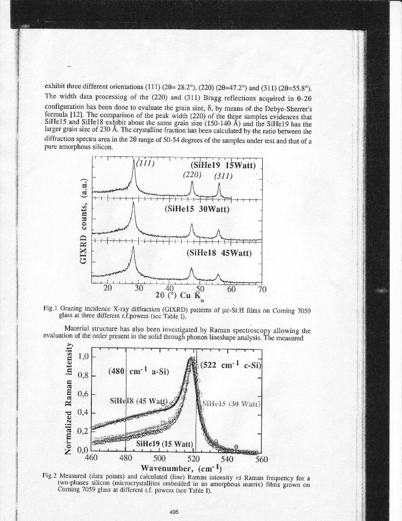
Material structure has also been investigated by Raman spectroscopy allowing theevaluation of the order present in the solid throug[ phonon lineshape analysis. the rneisureA
.A
I
Xr h
50CUK
>.(a
q)
(uN
L
z
1,0
0,8
0,6
0,4
0,2
4bu 480 500 520 540Wavenunrber, (cm'r;
Fig.2 Measured (data points) and calculated (line) Raman intensitv vstwo-phases silicon (microcrystallites ernbetkjed in an amorphbusComing 7059 glass at different. r.f. powers (see Table I).
560
Raman frequency for amatrix) films grown on
III) (siHerg tswatt)(220) (3rr)
(SiHe15 30Watt)
(SiHe18 45Watt)
cm'1 a-S i )
I (45 \VaS)
, (522 cm- l c-Si
i ;9 l l '1 . - t ' * t f )
SiHel9 (15 Watt)0,0
495

spectra (data points), shown in Fig.2, are characterized by a rather sharp peak around 520 cm-lwith a low-frequency tail, typical for microcrystalline silicon. Such lineshapes are related to thephonon confinement in srnall domain sizes which induces a partial relaxation of single crystalphonon selection rules, allowing the involvement of a large range of phonons with differentmomentum to the scattering process. It has been reported by several authors [13, 14] that sucha model gives a reasonable estimation of the confinement size and hence of the averagecrystallite size. However, assuming a single size of confinement, the predicted asymmetricbroadening and frequency downshift have not been consistent with the experimental findings.This result indicates that the material structure is not homogeneous but crystallites of differentsizes are formed during the growth. In particular, it is reasonable to assume that large-sizedsilicon nanocrystallites are surrounded by small-sized ones, or embedded in an amorphoustissue. In such a case a bimodal crvstallite size distribution function
G(R) = (1-y) d(R-R1) + y d(R-R2) ( 1 )can be assumed indicating that the fractions y and (1-y) of the sarnple are constituted by R2-sized and R1-sized nanocrystallites, respectively. The intensity profile of the Raman band canbe then written:
I(rrr) = C J On GG) S(to, R)where C is a proper constant and S(co, R) is the crystallite lineshape function. Assuming aGaussian confinement and a spherical Brillouin zone [15], the latter function can be written
f 's1ro, n; = {
dq 4nq2e-(qnl'r+ - (3)' J" 'r
- a(il12+ (yl2)2
where q is the normalized phonon momentum, co(q) is a one-dimensional average of the optical
phonon branch dispersion curves and 1is the phonon line-width. Raman lineshapes can bereproduced fairly well by eqs.(2), (3) (continuous line in Fig. 2) assuming an effective
dispersion curve o(q) = 480 + 40 cos (pq) tcm-ll. Such a curve is able to predict the Ramanlineshapes the broad R4man feature at 480 s6-1, characteristic of amorphous silicon, for aconfinement size of 22 A,in agreement with previous reports tl6l. All the iirvestigated sampleshave been analyzed in the frame of this model. Only for the sample SiHel5 it was necessary totake into account also stress effects in order to obtain a satisfying fit of data. In particular acompressive hydrostatic stress was assumed, leading to a rigid shifting of the phonondispersion curve by I cm-I.
Energy, (eV)Fig. 3 The irnaginary part, <€2> of the pseudo-dielectric function vs the energy for pc-Si films
obtained at three different r.f. powers.
(2)
30
25
nc*r^ I 5
20
10
0
SiHe19
FiiHe 18
l i i i t r*{rr i
496

Figure 3 shows the imaginary par!, ,1t?? of .the pseudo-dielectric function, uncorrectedfor surfac-e roughness, recorde-cl foithe SiHelg, SiHel5 and SiHel8 samples. It is evident a
decrease of the <t2> specfra and a broadening of the E1 and E2.interbandcritr,cal points which
sussest a reductioi of'both the crystalline friction and the glain size, goin-g from the SiHel9
;frtt. to the SiHel8 sample. T[is behaviour is confirmed by the best fit BEMA models,
which consist of a bulk pc-Si layer, including a mixture of pc-Si + a-Si + voids, and a rough
surface layer simulated by (pc-Si + voids). The resulting data of the crystailine volume-fraction
of the buik-layer for the three samples are listed in Table I. In the Table, it has also beenspecifred that iccording to XRD and-Raman data large-grain polycrystalline siliqon componenta'pplies for the SiHe19-sample, whereas fine-grain polycrysialline silicon applies for SiHe15and SiHel8 samples.
The specific features found in the formation of microcrystalline silicon from the Headdition to 1hg Sif4-H2 mixtures are: the enhancement of crystallization and the production ofunstressed crystalline material under mild plasma conditions such as low r.f. power and low
deposition temperature (120 'C). At this low value temperature grain size, 6, and crystalline
uoiu*e fraction, fr, increase by decreasing the power and, in pa1gg_u-lar, a pure or highlycrystalline material-(f. - I00 Vo) is deposited at r.f. power.as low as 15 Watt '
" Figure 4 shows the crystallin-e fraction, fs, tS o function of net deposition rate rD atwhich the"silicon films are grown. In this plot, we can distinguish three regions, the first at
deposition rate values less tfian 0.3 A/sec, in which pure microcrgstalline, phase exists in the
miterial, the second at deposition rate values in the range 0.3-0.2 A,/sec where the amorphousunO rnicio.rystalline phases coexist at variable percentages; in particular the microcrystalline
- 100N
.*- " 80
.i 60q)
trc- 40
q)
?20(h
>.L
r \ I t
0 0,2 0,4 0,6 0,8 ̂ | 1,2Net deposition rate, rD (A/sec)
Fig. 4 Crystalline fraction of silicon films vs the net deposition rate at which the material is grown'
phase decreases by increasing the deposition rate. The third at deposition rate greater than 1A/r.r, where pure-amorphouJphase is obtained t9l. In pure micro-rystalline region, the grainsize could furtherly increase at lower deposition mte, since the deposition rate and thecrystallitesize are inversely proportional, as found by G. Bruno et al. [17] in a similar halogenatedsystem. The net deiosition rate value, ra, which is the difference befween the.growth rate, rG,aitd th" etching rati, ry, is determinant in establishing the material structure. At low values ofrD, the selectiv:e etching of amorphous phase with respect to the crystalline-by F- an{ ll-atoms
6co*es operative as rJporred inref. 8, by enhancing the amorphous/crystalline.transition.Miirocrystallinify also has a characteristic signature in the FTIR: when the silicon fiIms
become *o.e and *o.e -mictocrystalline,
the total hydrogen content decreases and the fesidual
497

H atoms. are principally. bglrded in dihydride structure indicating accumulation ro the grainboundaries (see Table^I). The hydrogen.and fluorine atoms play a key role by promoting astructural order in the Si networkand are incorporated in the mlateiial at values Obtween 13 and6 at.Vo and less than lat.Vo, respectivelv.
The achievemert of h.ighly.crysiallized films is furtherly demonsffated by the Arrheniusdependence of the dark-conduttivity on the temperature for thL three samples with different f.and the same thickness; as the crystalline-volume fraction, fs, increases, tire dark-conductivit|and the mobility increase. Samirles having high crysraliiriity, e.g. sample SiHelg, ixhibitmobility values around 60 cm2V-1.
CONCLUSIONS
An enhancement of the amorphous to microcrystalline phase transition in silicon occurswhen helium is added to SiFa-H2 mixture. Helium pio-otes
'u ttigt concentration of F-atoms
*lli:l,areetchant.species se.lectivefor.amorphous pilase. We founf experimentaiconaitions inwnlcn nlgh-crystatltne traction is obtained at very low deposition temperature (120 oC) and atvery low r.f. power (15 Wan), as evaluated by XRD, Raman and ellips'om.t y tii["iq"i,r.
ACKNOWLEDGMENTS
The financial supports from Progetto Finalizzato CNR "Materiali Speciali perTecnologie Avanzate II'' and European-Joule Contract (JoR3-Cigi-gias-fr-ESTI hr"acknowledged.
REFERENCES
l.T.T9yqra, T. Matsui, Y. Kurokawa, H. okamoto and y. Hamakawa, Appl. phys. Lett.69, t26t (1996).
2 Q.^cig{-a, P. capezzuto, G. Bruno, L. schiavulli, G. perna and v. Capozzi,J. Appl. phys.80, 6564 (1996-).J. Meier,.R.,Fluckiger, H, K.eppner and A. shah, Appr. phys. Lett. 65, g60 (lgg4).s. -veprek, M. Heintze, F.-A. sarott, M. Jurcik-Rajman aira p. willmott, in Amorphousfi\on,Technology, edited b-y- A. Madan, u. L ttrompson, p. C. raytoi,'p."c.Lecomber and Y. Hamakawa (Mater. Res. soc. proc. llg, pittsburgh, ra, l"9ss) pp. 3-17 .
A. Matsuda, Thin Solid Films 332, xx (1999)c. c. Tsai, R. Thompson , c. Doland, F. A. ponce, G. B. Anderson, B. wacker inAmoryhous silicon Technology, edited by_ A. Madan, M. J. Thompson, p. c. rayroi, l.G. Lecomber and Y. Hamakawa (Mater."Res. soc. proc. llg, pittiburgh, pA, rq'ggibp.49-54.
7. M. Otobe, M. Kimura and S.Oda, Jpn.-J. Appl. phys. 31,4442 (lgg4).8. G. Cicala, l. ?p"""rto aqd G Bruno, Thiri bofid Fihs 332, f if qqAi.?:C,..Bjulg, P. Capezzuto, G. Cicata, J. Appl. phys.69, jZ56(lggt). '
10. H. P. Klyg.L. E. in Alexander, X-ray Dffiaciion P'rocedures, (New York John Wiley&Sons, 1914).
11 G_.E.Jellison, M.F. chisholm, s. M. Gorbatkin, Appl. phys. Lett.62, t4g3 (1993).12. P,.S, Baglay, D. E. Aspnes, A. C. Adams, C.'j. I4ogab, Appl. ffrys. Liti.-lg, SO(1981) .
l1 I, q Campbe.f], P. M. Faucher, Solid State Commun. 5g, 739 (19g6).14. J. Gonzalez-Hernandez, G. H. Azarbayejani, R. Tsu, F. H. pollaik, Appl. phys. Lett.
47 ,1350 (1985) .l5 4. Richter,Z.P. Wang,.L. Ley, Qolid State Commun.39,625 (19g1).16 c. lr4essana, B. A. De Angeli-s, G. conte, c. Gramaccioni, L it ys. b 14, Lgl-4 (l9gl)
and refs. therein.17. G. Bruno, P. capezzuto and F. cramarossa, Thin solid Films 106, 145 (19g3).
3.4.
5.6.
'1!i*
,*
ffi
498
Related Documents