Enhanced second harmonic generation from InAs nano-wing structures on silicon† Emanuele Francesco Pecora, a Gary F. Walsh, ab Carlo Forestiere, ac Alex Handin, a Eleonora Russo-Averchi, d Anna Dalmau-Mallorqui, d Ignasi Canales-Mundet, b Anna Fontcuberta i Morral d and Luca Dal Negro * a We demonstrate morphology-dependent second-harmonic genera- tion (SHG) from InAs V-shaped nanomembranes. We show SHG correlation with the nano-wing shape and size, experimentally quantify the SHG efficiency, and demonstrate a maximum SHG enhancement of about 500 compared to the bulk. Experimental data are supported by rigorous calculations of local electromagnetic field spectra. Introduction Nonlinear optical phenomena have been recently exploited in order to demonstrate photon manipulation on a single chip, where new functionalities such as parametric down-conver- sion, optical broadband routing, and multiple frequency generation can potentially be integrated. 1–4 In particular, the second harmonic generation (SHG) process, which originates from the second-order optical susceptibility c (2) of materials, enables the conversion of two photons (usually in the near-IR wavelength range) into a single photon of doubled frequency. Many different semiconductor materials exhibit large second- order susceptibility, but they cannot easily be integrated with the widespread Si-based microelectronics technology. On the other hand, bulk Si possesses only a negligible c (2) due to its centrosymmetric crystal structure, which makes it unsuitable for efficient nonlinear optical generation on a chip. Neverthe- less, a signicant amount of research activities have demonstrated promising strategies to boost optical nonlinear- ities in Si-based materials systems. Recently, enhanced second- order nonlinearity in Si has been demonstrated by a number of approaches including higher-order multipolar processes, 5 the breaking of crystal symmetry at interfaces, the engineering of strain elds, 6–12 or the development of substoichiometric silicon nitride thin lms. 13 An alternative strategy relies on the inte- gration atop Si technology of non-centrosymmetric semi- conductor nanostructures that feature very efficient optical nonlinear coefficients, thus potentially enabling a number of novel device applications. In particular, III–V semiconductors monolithically grown on Si-compatible substrates are already utilized for specic optoelectronics applications due to their direct band-gaps and high carrier mobilities. 14–16 Moreover, III–V semiconductor materials can be synthesized in a large variety of nanostructures with different sizes, shapes, architectures, and compositions, resulting in largely tunable quantum size effects and morphology-driven optical resonances that permit to exibly engineer light–matter interactions. In particular, three-dimen- sional structures such as nanowires, 17–21 nanotrees, 22 nanorings, 23 nanoowers, 24,25 or nanomembranes 26 have shown signicant advantages over traditional quantum dots and quantum wells due to their ability to support tunable resonances that enhance their optical properties. 27–30 A number of studies have been per- formed on the linear optical properties of III–V nanostructures, but little is known on the interplay between morphology- dependent structural resonances and their nonlinear optical properties. In this paper, we systematically investigate the second harmonic generation in InAs V-shaped nanomembranes, dub- bed nano-wings, grown epitaxially on (001) Si substrates. By investigating a number of samples fabricated with varying geometrical parameters, we correlate the measured SHG signal and efficiency to the shape and size of the nano-wings, demonstrating a maximum SHG signal enhanced by about 500 times compared to a reference InAs bulk sample due to the excitation of structural resonances with large local eld enhancement at the pump wavelength. a Department of Electrical and Computer Engineering & Photonics Center, Boston University, 8 Saint Mary Street, Boston, Massachusetts 02215, USA. E-mail: [email protected] b Nanomaterials Science Team, U.S. Army NSRDEC, Kansas Street, Natick, Massachusetts 01760, USA c Department of Electrical Engineering and Information Technology, Universit` a degli Studi di Napoli Federico II, via Claudio 21, Napoli 80125, Italy d Laboratoire des Mat´ eriaux Semiconducteurs, Ecole Polytechnique F´ ed´ erale de Lausanne, 1015 Lausanne, Switzerland † Electronic supplementary information (ESI) available: See DOI: 10.1039/c3nr03083k Cite this: Nanoscale, 2013, 5, 10163 Received 14th June 2013 Accepted 23rd August 2013 DOI: 10.1039/c3nr03083k www.rsc.org/nanoscale This journal is ª The Royal Society of Chemistry 2013 Nanoscale, 2013, 5, 10163–10170 | 10163 Nanoscale COMMUNICATION Published on 27 August 2013. Downloaded by Boston University on 17/10/2013 05:29:33. View Article Online View Journal | View Issue

Welcome message from author
This document is posted to help you gain knowledge. Please leave a comment to let me know what you think about it! Share it to your friends and learn new things together.
Transcript
Nanoscale
COMMUNICATION
Publ
ishe
d on
27
Aug
ust 2
013.
Dow
nloa
ded
by B
osto
n U
nive
rsity
on
17/1
0/20
13 0
5:29
:33.
View Article OnlineView Journal | View Issue
aDepartment of Electrical and Computer E
University, 8 Saint Mary Street, Boston
[email protected] Science Team, U.S. Ar
Massachusetts 01760, USAcDepartment of Electrical Engineering and
Studi di Napoli Federico II, via Claudio 21,dLaboratoire des Materiaux Semiconduct
Lausanne, 1015 Lausanne, Switzerland
† Electronic supplementary informa10.1039/c3nr03083k
Cite this: Nanoscale, 2013, 5, 10163
Received 14th June 2013Accepted 23rd August 2013
DOI: 10.1039/c3nr03083k
www.rsc.org/nanoscale
This journal is ª The Royal Society of
Enhanced second harmonic generation from InAsnano-wing structures on silicon†
Emanuele Francesco Pecora,a Gary F. Walsh,ab Carlo Forestiere,ac Alex Handin,a
Eleonora Russo-Averchi,d Anna Dalmau-Mallorqui,d Ignasi Canales-Mundet,b
Anna Fontcuberta i Morrald and Luca Dal Negro*a
We demonstrate morphology-dependent second-harmonic genera-
tion (SHG) from InAs V-shaped nanomembranes. We show SHG
correlation with the nano-wing shape and size, experimentally
quantify the SHG efficiency, and demonstrate a maximum SHG
enhancement of about 500 compared to the bulk. Experimental data
are supported by rigorous calculations of local electromagnetic field
spectra.
Introduction
Nonlinear optical phenomena have been recently exploited inorder to demonstrate photon manipulation on a single chip,where new functionalities such as parametric down-conver-sion, optical broadband routing, and multiple frequencygeneration can potentially be integrated.1–4 In particular, thesecond harmonic generation (SHG) process, which originatesfrom the second-order optical susceptibility c(2) of materials,enables the conversion of two photons (usually in the near-IRwavelength range) into a single photon of doubled frequency.Many different semiconductor materials exhibit large second-order susceptibility, but they cannot easily be integrated withthe widespread Si-based microelectronics technology. On theother hand, bulk Si possesses only a negligible c(2) due to itscentrosymmetric crystal structure, which makes it unsuitablefor efficient nonlinear optical generation on a chip. Neverthe-less, a signicant amount of research activities have
ngineering & Photonics Center, Boston
, Massachusetts 02215, USA. E-mail:
my NSRDEC, Kansas Street, Natick,
Information Technology, Universita degli
Napoli 80125, Italy
eurs, Ecole Polytechnique Federale de
tion (ESI) available: See DOI:
Chemistry 2013
demonstrated promising strategies to boost optical nonlinear-ities in Si-based materials systems. Recently, enhanced second-order nonlinearity in Si has been demonstrated by a number ofapproaches including higher-order multipolar processes,5 thebreaking of crystal symmetry at interfaces, the engineering ofstrain elds,6–12 or the development of substoichiometric siliconnitride thin lms.13 An alternative strategy relies on the inte-gration atop Si technology of non-centrosymmetric semi-conductor nanostructures that feature very efficient opticalnonlinear coefficients, thus potentially enabling a number ofnovel device applications. In particular, III–V semiconductorsmonolithically grown on Si-compatible substrates are alreadyutilized for specic optoelectronics applications due to theirdirect band-gaps and high carrier mobilities.14–16 Moreover, III–Vsemiconductor materials can be synthesized in a large variety ofnanostructures with different sizes, shapes, architectures, andcompositions, resulting in largely tunable quantum size effectsand morphology-driven optical resonances that permit to exiblyengineer light–matter interactions. In particular, three-dimen-sional structures such as nanowires,17–21 nanotrees,22 nanorings,23
nanoowers,24,25 or nanomembranes26 have shown signicantadvantages over traditional quantum dots and quantum wellsdue to their ability to support tunable resonances that enhancetheir optical properties.27–30 A number of studies have been per-formed on the linear optical properties of III–V nanostructures,but little is known on the interplay between morphology-dependent structural resonances and their nonlinear opticalproperties.
In this paper, we systematically investigate the secondharmonic generation in InAs V-shaped nanomembranes, dub-bed nano-wings, grown epitaxially on (001) Si substrates. Byinvestigating a number of samples fabricated with varyinggeometrical parameters, we correlate the measured SHG signaland efficiency to the shape and size of the nano-wings,demonstrating a maximum SHG signal enhanced by about 500times compared to a reference InAs bulk sample due to theexcitation of structural resonances with large local eldenhancement at the pump wavelength.
Nanoscale, 2013, 5, 10163–10170 | 10163
Nanoscale Communication
Publ
ishe
d on
27
Aug
ust 2
013.
Dow
nloa
ded
by B
osto
n U
nive
rsity
on
17/1
0/20
13 0
5:29
:33.
View Article Online
MethodsGrowth
The InAs membranes have been grown by molecular beamepitaxy in a DCA P600 system. We have used (001) p-dopedsilicon wafers with a resistivity of 0.1–0.5 U cm on which wedeposited a 20 nm thick SiO2 layer of thermal oxide as agrowth mask. Electron beam lithography has been used topattern holes with diameters ranging between 100 and 180 nmand inter-hole distances ranging from 200 to 2000 nm in a ZEPresist. The pattern has been then transferred on the oxidelayer by a 12 s 7 : 1 buffered HF wet etch. Prior to the intro-duction to the MBE reactor, the wafer underwent a further 2 sdip in the buffered HF solution in order to guarantee aperfectly clean and oxide-free surface in the holes. Thesubstrates were subsequently degassed at 600 �C for 2 h inUHV and then again at 770 �C for 30 min when transferred tothe growth chamber to further remove any possible surfacecontaminants. The growth was carried out at a nominal Ingrowth rate of 0.2 A s�1, at a temperature of 520 �C, As4 partialpressure of 0.8 and 1.15 � 10�5 Torr (growth time respectivelyof 1 h and 2 h) and with 7 rpm rotation.
Optical set-up
Second harmonic generation has been studied using a mode-locked high power ultrafast Ti:sapphire laser (MaiTai HPSpectraPhysics, 150 fs pulse width) coupled with an electro-optic pulse picker to set the repetition rate at 20 MHz. Theaverage pumping power was 8 mW, laser light was horizontalpolarized, and the excitation wavelength in the range 700–900nm. We ensured that no thermal oxidation occurred underthese conditions, and measures were repeatable in the samespot aer sweeping the pump power several times. The pumpbeam was focused on the sample using a 20� microscopeobjective, unless otherwise specied in the text. The sameobjective was used to collect the back-reected light. A long-passlter was placed before the sample to avoid any unrelated signalat the second harmonic wavelengths. The sample output wascollected through a standard telescoping lens arrangement andcoupled into an f/4 monochromator (Cornerstone 260). Thepump light was rejected by a short-pass lter placed in front ofthe monochromator slits. The SHG spectra have been detectedwith a lock-in amplier (Oriel Merlin) coupled to a low-lightphotomultiplier tube (PMT, Oriel Instrumentation 77348). TheSHG output power has been estimated considering the PMTresponsivity, the measured transmittivity of all the opticalcomponents and the light coupling efficiency into the mono-chromator, and also directly measured through a highly sensi-tive power meter detector (Newport 918D-UVOD3), as reportedelsewhere.13 The same set-up was also used for imaging andaligning the sample in order to ensure overlap between the laserbeam-illuminated area and the nanostructure area in thesample. For this purpose, the output of the objective was sentalso to a visible-sensitive camera and the alignment was veriedbefore every measure. A schematic of the experimental set-up issketched in the ESI, Fig. SI1.†
10164 | Nanoscale, 2013, 5, 10163–10170
Modeling
Electromagnetic scattering calculations were performed using aSurface Integral Formulation of Maxwell's equations. They veryeffectively treat the scattering from arbitrary shaped particlessince they require only the discretization of the spatial domainoccupied by the scatterers, while the radiation conditions areautomatically satised. A detailed comparison of the accuracyof several Surface Integral Formulations in both the far and neareld zone is reported elsewhere.31 The calculations performedin this paper are based on the PMCHWT (Poggio, Miller, Chang,Harrington, andWu) formulation.32,33 In this work, meshes withabout 4k edges have been used to numerically solve the scat-tering problem.
Results and discussionNanomembranes growth and structural characterization
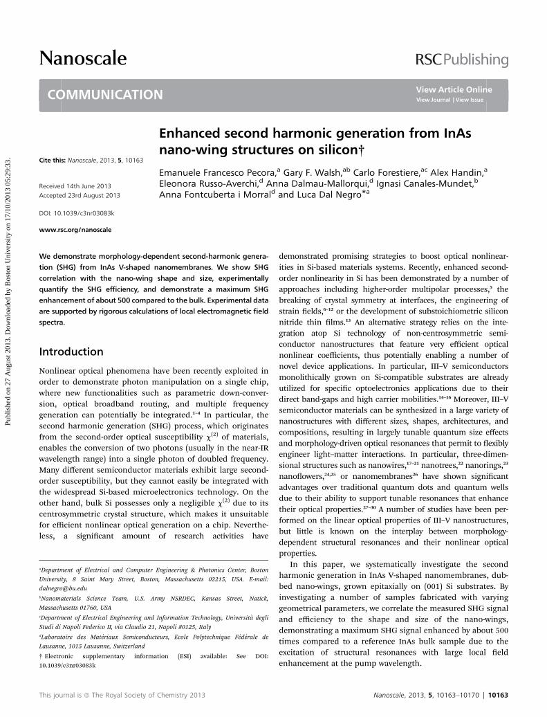
Fig. 1 shows 20� tilted scanning electron microscopy (SEM)images of typical InAs membranes grown at 520 �C, nominal Ingrowth rate of 0.2 A s�1 and under As4 partial pressure of 0.8 �10�5 Torr (a – 1 h growth) and 1.15 � 10�5 Torr (b – 2 h growth).The images reveal the peculiar shape of the nanostructures withtwo preferred directions of elongation. The structural propertiesof these nanosctructures have already been discussedelsewhere.26,34
They present a mixture of wurtzite and zinc-blende structure,and extend along two opposite <111> B directions, forming at{110} walls. In particular, in a top-down projection, we foundtwo comparable distribution of membranes, extending respec-tively along the <1�10> and <110> directions. The directionperpendicular to the substrate and parallel to the incident lightis the (100). As the excitation beam is linearly polarized, we willalways observe a combination of the longitudinal and trans-verse mode on the nanostructures. As described in the experi-mental section, the membranes are positioned in regular holesarrays in a SiO2 mask with diameter changing from 100 to180 nm and inter-hole distance (pitch) changing from 200 to2000 nm. Fig. 1(c) and (d) show the effect of the pitch and theopening size on the size of membranes grown under theconditions mentioned above (in blue: As4 partial pressure of 0.8� 10�5 Torr for 1 h, in red: As4 partial pressure of 1.15 � 10�5
Torr for 2 h). Both the samples are characterized by a signicantlength variation as a function of the pitch (Fig. 1(c)). Thisdependence is characterized by two separate growth regimes asit has been found by other groups for nanowires grown onpattern:35–37 for pitches below 800 nm the length increases withthe pitch, while above that threshold the length saturates. Theswitch between the two regimes is determined by the indiumsurface diffusion length on the SiO2. A detailed description ofthis mechanism is discussed in a separate work.34 The effectof the hole size on the morphology of the membranes isdescribed in Fig. 1(d): the width of the membranes increases byincreasing the opening sizes. As noted in Conesa-Boj et al.26 themembranes originate from the two opposite facets of a rectan-gular pyramidal island nucleus, the size of which is in turndetermined by the opening size. As for the dependence of the
This journal is ª The Royal Society of Chemistry 2013
Fig. 1 Scanning electron microscopy (SEM) tilted (20�) images of typical InAsmembranes grown at 520 �C, nominal In growth rate of 0.2 A s�1 and under As4partial pressure of 0.8 � 10�5 Torr (a – 1 h growth) and 1.15 � 10�5 Torr (b – 2 hgrowth). Effect of the pitch on the length of InAs membranes: the lengthincreases by increasing the pitch and saturates (c). Plot of the membranes widthas a function of the opening size: the width increases by increasing the openingsize (d).
This journal is ª The Royal Society of Chemistry 2013
Communication Nanoscale
Publ
ishe
d on
27
Aug
ust 2
013.
Dow
nloa
ded
by B
osto
n U
nive
rsity
on
17/1
0/20
13 0
5:29
:33.
View Article Online
length on the pitch, a detailed description of this behavior willbe provided in a dedicated study.
Electromagnetic modeling
Using the accurate surface integral equation (SIE) method,31–33
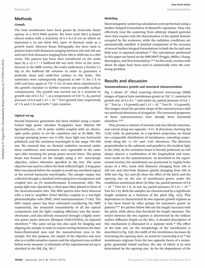
we investigate the scattering and near eld behaviour of nano-wings as a function of incident wavelength, rst by varying thelength of the nano-wing for xed widths and then by varying thewidth for xed lengths. Engineering the distinctive scatteringand near-eld response of dielectric nano-wing structures is ofimportance for tailoring their linear and nonlinear opticalproperties, as it will be demonstrated in the next section. Weexcited the nano-wing with a plane wave of unit intensitypropagating in the negative z-direction for two different polar-izations, longitudinal (x-polarized with reference to Fig. 2) andtransverse (y-polarized) to the length of the nano-wing. Fig. 2(a)and (b) show the scattering efficiency as a function of wave-length for different nano-wing lengths with a xed width of75 nm for longitudinal and transverse excitation respectively.For both longitudinal and transverse excitation, we can see aresonant behaviour controlled by the geometrical parameters ofthe nano-wing. As the length increases from 1850 nm to 3615nm, the peak value of the scattering efficiency also increases,and in the case of longitudinal polarization undergoes asubstantial red-shi. Fig. 2(c) and (d) show the scattering effi-ciency as a function of wavelength for different nano-wing widthwith a xed length of 1600 nm for longitudinal and transverseexcitation respectively. For longitudinal polarization, as thewidth increases from 50 nm to 160 nm the peak value decreases,whereas we found no signicant trend for the transversepolarization. For both polarizations we observe a strong red-shi. In conclusion, we have shown a resonant scatteringbehaviour of the nano-wing driven by its geometrical parame-ters. We now investigate the near-eld distribution of the nano-wing resonances, and show that they can signicantly enhancethe local intensity of incident electric elds. Fig. 3(a) and (b)show the total electric eld (sum of incident and scattered eld)plotted on the surface of the nano-wing for the longitudinal andtransverse modes respectively. We calculated the surface eldwith a single incident wavelength of 800 nm for a nano-wingwith a length of 1150 nm and a width of 75 nm. When theincident eld is longitudinally polarized, the total eld on thesurface of the nano-wing is strongly localized at the two tipsand along the edges of the faces. In the case of a transverseincident polarization the total eld is more uniformlydistributed on the vertical faces of the nano-wing, although itassumes lower values compared to the longitudinal excitationconguration. Fig. 3(c) and (d) show the average of the surfaceelectric eld as a function of wavelength for different nano-wing lengths with a xed width of 75 nm for longitudinal andtransverse excitation respectively. For longitudinal excitation,at a wavelength of 800 nm, as the length increases from 1850nm to 3615 nm, the average electric eld decreases. Ouranalysis unveils that a clear trend exists: the shortest nano-wing features the largest average surface electric eld. Fortransverse excitation, no clear trend exists for the investigated
Nanoscale, 2013, 5, 10163–10170 | 10165
Fig. 2 Spectrum of the scattering efficiency as a function of wavelength for different nano-wing lengths with a fixed width of 75 nm for longitudinal (a) and transverseexcitation (b) respectively. Spectrum of the scattering efficiency as a function of wavelength for different nano-wing widths with a fixed length of 1600 nm forlongitudinal (c) and transverse (d) excitation. The nano-wing is excited with a plane wave of unit intensity propagating in the negative z-direction.
Nanoscale Communication
Publ
ishe
d on
27
Aug
ust 2
013.
Dow
nloa
ded
by B
osto
n U
nive
rsity
on
17/1
0/20
13 0
5:29
:33.
View Article Online
set of parameters. The structure with largest average electriceld has a length of 800 nm while the other structures haveapproximately the same eld strength.
Second harmonic experiments
In this section we investigate the second harmonic generation(SHG) from nano-wing samples supporting tunable near-eldand scattering resonances spectrally overlapping the pumpwavelength. The possibility to signicantly enhance and controlthe SHG of nano-wings by tailoring their nanoscale morphologywill be experimentally demonstrated. The second harmonicgeneration takes place in both the surface and the bulk of theInAs nanostructures. Both bulk and surface sources of nonlin-earity can be strongly inuenced by the local distribution of theelectric eld on the surface and within the bulk of the InAsnanostructures, as a result of their resonant optical response.We notice that, in the case of crystalline InAs, materials, theo-retical considerations44 suggest that the bulk contribution tothe second harmonic generation dominates over the surfacecontribution. This has been conrmed by experimental resultsof SHG in planar InAs slabs.38 On the other hand, little is knownon the relative contributions of bulk versus surface nonlinearcontributions in resonant nanostructures with non-sphericalshapes, such as the investigated nano-wings, and a systematicexperimental study is proposed in this section. In Fig. 4(a) we
10166 | Nanoscale, 2013, 5, 10163–10170
show representative second harmonic (SH) spectra recordedfrom a sample with a 500 nm span of the nano-wings (from hereon referred to as the length of the nano-wing), and wingthicknesses in the range between 95 nm and 180 nm. It is worthnoting that the average pump power used to generate the SHsignal in the paper was only 8 mW (800 nm excitation wave-length). The SH signal detected from a bulk InAs wafer underexactly the same experimental conditions is also reported as areference (spectrum has been multiplied by 20 to be visible inthe plot). In particular, our substrate is (001) oriented and wemeasured the azimuthal angle of the SH emission in order toidentify the angle corresponding to the highest SH intesity.38 Weshow in Fig. SI2† the trend with the azimuthal angle of our data.The measured signal from the nanostructures is consistently atleast one order of magnitude higher than from the bulk mate-rial. Moreover, it is important to observe that no scaling factorhas been applied to these data, despite the illuminated materialvolume is much smaller in the nano-wing samples compared tothe reference bulk material. This demonstrates that the V-shapemorphology of the nano-wings plays a fundamental role inenhancing the SH emission. Furthermore, we observe a cleartrend between the SH intensity and the thickness of the nano-wings, establishing a correlation between the structuralparameters of the wings and their enhanced nonlinear opticalresponses. We discovered that the strongest SH signal isgenerated by the thinnest nano-wings. In addition, in Fig. 4 we
This journal is ª The Royal Society of Chemistry 2013
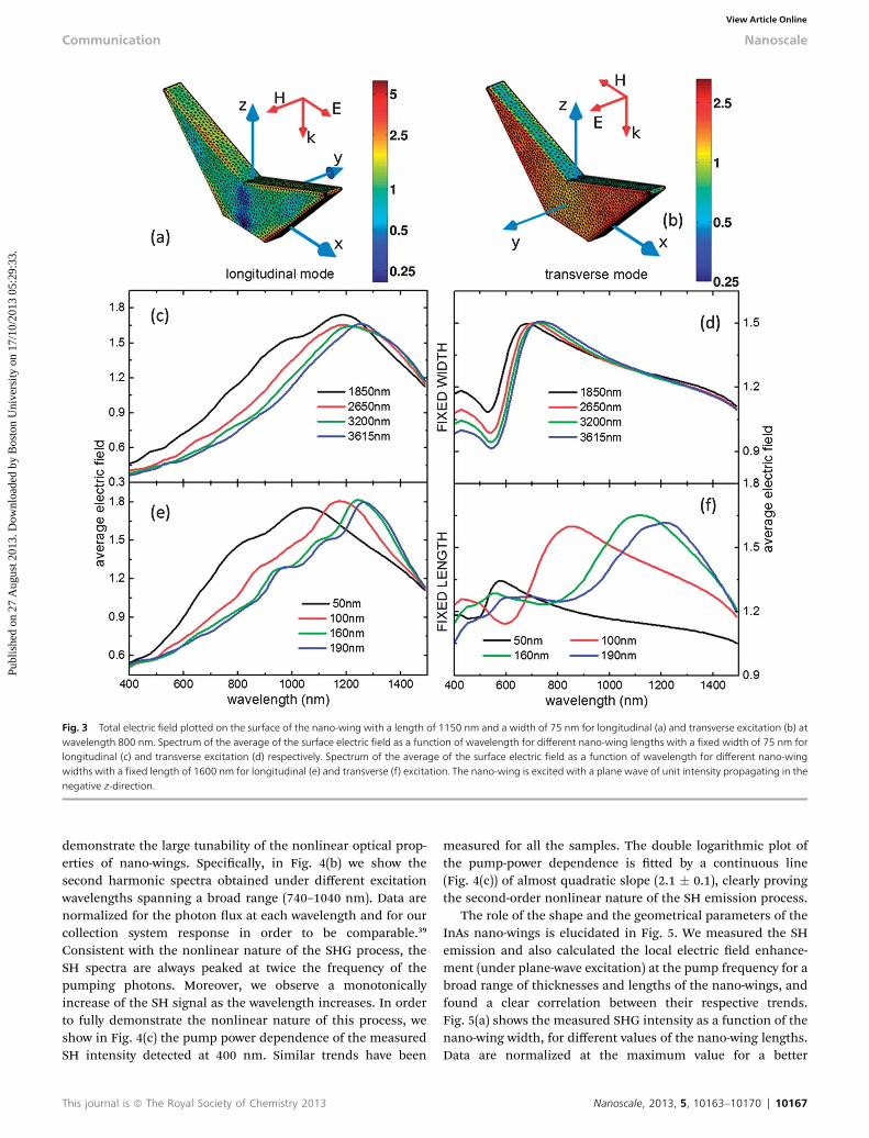
Fig. 3 Total electric field plotted on the surface of the nano-wing with a length of 1150 nm and a width of 75 nm for longitudinal (a) and transverse excitation (b) atwavelength 800 nm. Spectrum of the average of the surface electric field as a function of wavelength for different nano-wing lengths with a fixed width of 75 nm forlongitudinal (c) and transverse excitation (d) respectively. Spectrum of the average of the surface electric field as a function of wavelength for different nano-wingwidths with a fixed length of 1600 nm for longitudinal (e) and transverse (f) excitation. The nano-wing is excited with a plane wave of unit intensity propagating in thenegative z-direction.
Communication Nanoscale
Publ
ishe
d on
27
Aug
ust 2
013.
Dow
nloa
ded
by B
osto
n U
nive
rsity
on
17/1
0/20
13 0
5:29
:33.
View Article Online
demonstrate the large tunability of the nonlinear optical prop-erties of nano-wings. Specically, in Fig. 4(b) we show thesecond harmonic spectra obtained under different excitationwavelengths spanning a broad range (740–1040 nm). Data arenormalized for the photon ux at each wavelength and for ourcollection system response in order to be comparable.39
Consistent with the nonlinear nature of the SHG process, theSH spectra are always peaked at twice the frequency of thepumping photons. Moreover, we observe a monotonicallyincrease of the SH signal as the wavelength increases. In orderto fully demonstrate the nonlinear nature of this process, weshow in Fig. 4(c) the pump power dependence of the measuredSH intensity detected at 400 nm. Similar trends have been
This journal is ª The Royal Society of Chemistry 2013
measured for all the samples. The double logarithmic plot ofthe pump-power dependence is tted by a continuous line(Fig. 4(c)) of almost quadratic slope (2.1 � 0.1), clearly provingthe second-order nonlinear nature of the SH emission process.
The role of the shape and the geometrical parameters of theInAs nano-wings is elucidated in Fig. 5. We measured the SHemission and also calculated the local electric eld enhance-ment (under plane-wave excitation) at the pump frequency for abroad range of thicknesses and lengths of the nano-wings, andfound a clear correlation between their respective trends.Fig. 5(a) shows the measured SHG intensity as a function of thenano-wing width, for different values of the nano-wing lengths.Data are normalized at the maximum value for a better
Nanoscale, 2013, 5, 10163–10170 | 10167
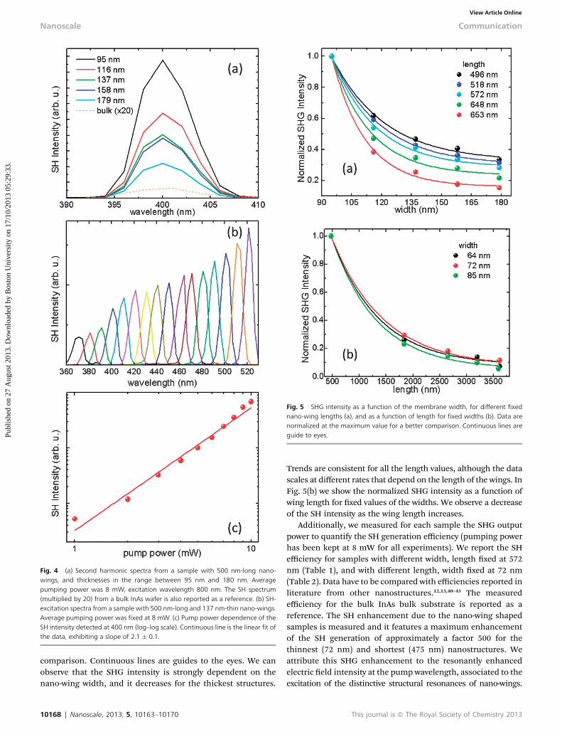
Fig. 4 (a) Second harmonic spectra from a sample with 500 nm-long nano-wings, and thicknesses in the range between 95 nm and 180 nm. Averagepumping power was 8 mW, excitation wavelength 800 nm. The SH spectrum(multiplied by 20) from a bulk InAs wafer is also reported as a reference. (b) SH-excitation spectra from a sample with 500 nm-long and 137 nm-thin nano-wings.Average pumping power was fixed at 8 mW. (c) Pump power dependence of theSH intensity detected at 400 nm (log–log scale). Continuous line is the linear fit ofthe data, exhibiting a slope of 2.1 � 0.1.
Fig. 5 SHG intensity as a function of the membrane width, for different fixednano-wing lengths (a), and as a function of length for fixed widths (b). Data arenormalized at the maximum value for a better comparison. Continuous lines areguide to eyes.
Nanoscale Communication
Publ
ishe
d on
27
Aug
ust 2
013.
Dow
nloa
ded
by B
osto
n U
nive
rsity
on
17/1
0/20
13 0
5:29
:33.
View Article Online
comparison. Continuous lines are guides to the eyes. We canobserve that the SHG intensity is strongly dependent on thenano-wing width, and it decreases for the thickest structures.
10168 | Nanoscale, 2013, 5, 10163–10170
Trends are consistent for all the length values, although the datascales at different rates that depend on the length of the wings. InFig. 5(b) we show the normalized SHG intensity as a function ofwing length for xed values of the widths. We observe a decreaseof the SH intensity as the wing length increases.
Additionally, we measured for each sample the SHG outputpower to quantify the SH generation efficiency (pumping powerhas been kept at 8 mW for all experiments). We report the SHefficiency for samples with different width, length xed at 572nm (Table 1), and with different length, width xed at 72 nm(Table 2). Data have to be compared with efficiencies reported inliterature from other nanostructures.12,13,40–43 The measuredefficiency for the bulk InAs bulk substrate is reported as areference. The SH enhancement due to the nano-wing shapedsamples is measured and it features a maximum enhancementof the SH generation of approximately a factor 500 for thethinnest (72 nm) and shortest (475 nm) nanostructures. Weattribute this SHG enhancement to the resonantly enhancedelectric eld intensity at the pump wavelength, associated to theexcitation of the distinctive structural resonances of nano-wings.
This journal is ª The Royal Society of Chemistry 2013
Table 1 Measured SH efficiency and SH enhancement compared to bulk InAs fornano-wings with different width and fixed length (572 nm)
Width (nm) SHG efficiency SHG enhancement
95 1.821 � 10�4 303116 1.129 � 10�4 188137 8.50 � 10�5 141158 7.88 � 10�5 131179 4.60 � 10�5 76Bulk 6 � 10�7 1
Table 2 Measured SH efficiency and SH enhancement compared to bulk InAs fornano-wings with different length and fixed width (72 nm)
Length (nm) SHG efficiency SHG enhancement
475 2.932 � 10�4 4881837 5.49 � 10�5 912655 5.33 � 10�5 883200 3.13 � 10�5 523615 1.15 � 10�5 19Bulk 6 � 10�7 1
Communication Nanoscale
Publ
ishe
d on
27
Aug
ust 2
013.
Dow
nloa
ded
by B
osto
n U
nive
rsity
on
17/1
0/20
13 0
5:29
:33.
View Article Online
On the other hand, based on the calculated scattering crosssections of nano-wings (see Fig. 2), the role of scattering resonancesat the SHG wavelength is negligible with respect to the pumpwavelength. While a rigorous theoretical analysis of the nonlineargeneration in nano-wing structures is beyond the scope of thispaper, we believe that our experimental demonstration of resonantcontrol and SHG enhancement in InAs nano-wing structures canresult in novel functionalities uniquely enabled by the engineeringof resonant electromagnetic elds at the nanoscale.
Conclusions
In this work we demonstrated tunable and strongly enhanced(up to 500 times) second harmonic generation from InAs nano-wings of varying geometrical parameters monolithically grownon a Si substrate. We studied the resonant behaviour of nano-wing structures by the rigorous calculation of morphologydependent scattering resonances and near-eld electromag-netic spectra, obtained using the surface integral equationtechnique. We experimentally investigated the secondharmonic generation in this novel type of resonant nano-structures and experimentally quantied their SHG efficiency,and show a direct correlation with the shape and size of thenano-wings. The monolithic integration of III–V semiconductornanostructures with enhanced nonlinear optical properties on aSi platform paves the way to novel device structures leveragingwith tunable optical resonances for nonlinear photon genera-tion on a chip.
Acknowledgements
This work was supported by the AFOSR program “Emitters forHigh Density Information Processing using Photonic-
This journal is ª The Royal Society of Chemistry 2013
Plasmonic Coupling in Coaxial Nanopillars” under Award no.FA9550-13-1-0011, and by the U.S. Army Research Laboratorythrough the Collaborative Research Alliance (CRA) for Multi-Scale multidisciplinary Modeling of Electronic materials(MSME). G.W. acknowledges the U.S. Army Natick SoldierResearch, Development, and Engineering Center, and theSMART Scholarship Program. NSRDEC PAO# U13-254. ERCStarting Grant UpCon, NCCR-QSIT, SNF through grant 143908.The authors thank P. Caroff and X. Wallart for sharing the InAsreference sample. E.F.P. and G.W. performed the experimentsand analyzed data. A.H. and C.F. carried out the simulations.E.R.A. and A.D.M. fabricated the samples; I.C.M. and E.R.A.characterized their dimensions. E.F.P. and L.D.N. wrote themanuscript in collaboration with all the authors. L.D.N.conceived the scientic question; L.D.N. and A.F.M. plannedthe set of experiments. All authors have given approval to thenal version of the manuscript.
Notes and references
1 R. L. Sutherland, Handbook of Nonlinear Optics, CRC Press,2003.
2 J. Leuthold, C. Koos and W. Freude, Nat. Photonics, 2010, 4,535.
3 M. A. Foster, A. C. Turner, J. E. Sharping, B. S. Schmidt,M. Lipson and A. L. Gaeta, Nature, 2006, 441, 960.
4 A. M. Armani, R. P. Kulkarni, S. E. Fraser, R. C. Flagan andK. J. Vahala, Science, 2007, 317, 783.
5 D. Guidotti and T. Driscoll, Nuovo Cimento Soc. Ital. Fis., D,1986, 8, 385.
6 S. V. Govorkov, V. I. Emel'yanov, N. I. Koroteev, G. I. Petrov,I. L. Shumay, V. V. Yakovlev and R. V. Khokhlov, J. Opt. Soc.Am. B, 1989, 6, 1117.
7 J. Y. Huang, Jpn. J. Appl. Phys., 1994, 33, 3878.8 M. Falasconi, L. C. Andreani, A. M. Malvezzi, M. Patrini,V. Mulloni and L. Pavesi, Surf. Sci., 2001, 481, 105.
9 J. Zhao, Q. Chen, Z. Chen, G. Jia, W. Su, Y. Jiang, Z. Yan,T. V. Dolgova, O. A. Aktsipetrov and H. Sun, Opt. Lett.,2009, 34, 3340.
10 C. Schriever, C. Bohley and R. B. Wehrspohn, Opt. Lett., 2010,35, 273.
11 S. A. Mitchell, M. Mehendale, D. M. Villeneuve andR. Boukherroub, Surf. Sci., 2001, 448, 367.
12 M. Cazzanelli, F. Bianco, E. Borga, G. Pucker, M. Ghulinyan,E. Degoli, E. Luppi, V. Veniard, S. Ossicini, D. Modotto,S. Wabnitz, R. Pierobon and L. Pavesi, Nat. Mater., 2012,11, 148.
13 E. F. Pecora, A. Capretti, G. Miano and L. Dal Negro, Appl.Phys. Lett., 2013, 102, 141114.
14 M. E. Groenert, C. W. Leitz, A. J. Pitera, V. Yang, H. Lee,R. J. Ram and E. A. Fitzgerald, J. Appl. Phys., 2003, 93, 362.
15 T. Martensson, C. P. T. Svensson, B. A. Wacaser,M. W. Larsson, W. Seifert, K. Deppert, A. Gustafsson,L. R. Wallenberg and L. Samuelson, Nano Lett., 2004, 4, 1987.
16 V. Mourik, K. Zuo, S. M. Frolov, S. R. Plissard,E. P. A. M. Bakkers and L. P. Kouwenhoven, Science, 2013,336, 1003.
Nanoscale, 2013, 5, 10163–10170 | 10169
Nanoscale Communication
Publ
ishe
d on
27
Aug
ust 2
013.
Dow
nloa
ded
by B
osto
n U
nive
rsity
on
17/1
0/20
13 0
5:29
:33.
View Article Online
17 A. M. Morales and C. M. Lieber, Science, 1998, 279, 208.18 M. S. Gudiksen, L. J. Lauhon, J. Wang, D. C. Smith and
C. M. Lieber, Nature, 2002, 415, 617.19 S. A. Dayeh, E. T. Yu and D. Wang, Nano Lett., 2007, 7, 2486.20 A. Irrera, E. F. Pecora and F. Priolo, Nanotechnology, 2009, 20,
135601.21 E. F. Pecora, N. Lawrence, P. Gregg, J. Trevino, P. Artoni,
A. Irrera, F. Priolo and L. Dal Negro, Nanoscale, 2012, 4, 2863.22 K. A. Dick, K. Deppert, M. W. Larsson, T. Martensson,
W. Seifert, L. R. Wallenberg and L. Samuelson, Nat. Mater.,2004, 3, 380.
23 X. Y. Kong, Y. Ding, R. Yang and Z. L. Wang, Science, 2004,303, 1348.
24 H. Zhang, G. P. Cao, Z. Y. Wang, Y. S. Yang, Z. J. Shi andZ. N. Gu, Nano Lett., 2008, 8, 2664.
25 Y. B. Li, Y. Bando and D. Golberg, Appl. Phys. Lett., 2003, 82,1962.
26 S. Conesa-Boj, E. Russo-Averchi, A. Dalmau-Mallorqui,J. Trevino, E. F. Pecora, C. Forestiere, A. Handin, M. Ek,L. Zweifel, L. R. Wallenberg, D. Ruffer, M. Heiss,D. Troadec, L. Dal Negro, P. Caroff and A. Fontcuberta iMorral, ACS Nano, 2012, 6, 10982.
27 H. Xiaoying, L. Jing, Z. Yong and A. Mascarenhas, J. Am.Chem. Soc., 2003, 125, 7049.
28 A. Irrera, P. Artoni, F. Iacona, E. F. Pecora, G. Franzo,M. Galli, B. Fazio and F. Priolo, Nanotechnology, 2012, 23,075204.
29 V. R. Almeida, C. A. Barrios, R. R. Panepucci and M. Lipson,Nature, 2004, 431, 1081.
30 Q. Wan, K. Yu, T. H. Wang and C. L. Lin, Appl. Phys. Lett.,2003, 83, 2253.
31 C. Forestiere, G. Iadarola, G. Rubinacci, A. Tamburrino,L. Dal Negro and G. Miano, J. Opt. Soc. Am. A, 2012, 29, 2314.
10170 | Nanoscale, 2013, 5, 10163–10170
32 R. Harrington, Time-Harmonic Electromagnetic Fields,Springer, 2007.
33 A. Poggio and E. Miller, Integral equation solutions for threedimensional scattering problem, in Computer Techniques forElectromagentics, ed. R. Mittra, Pergamon Press, NY, 1973, ch. 4.
34 E. Russo-Averchi, A. Dalmau-Mallorquı, I. Canales-Mundet,G. Tutuncuoglu, E. Alarcon-Llado, M. Heiss, D. Ruffer,S. Conesa-Boj, P. Caroff and A. Fontcuberta i Morral,Nanotech., 2013, in press.
35 S. Hertenberger, D. Rudolph, M. Bichler, J. J. Finley,G. Abstreiter and G. Koblmuller, J. App. Phys., 2010, 108,114316.
36 M. T. Borgstrom, G. Immink, B. Ketelaars, R. Algra andE. P. A. M. Bakkers, Nat. Nanotechnol., 2007, 2, 541.
37 B. Bauer, A. Rudolph, M. Soda, A. Fontcuberta i Morral,J. Zweck, D. Schuh and E. Reiger, Nanotechnology, 2010, 21,435601.
38 M. Reid, I. V. Cravetchi and R. Fedosejevs, Phys. Rev. B:Condens. Matter Mater. Phys., 2005, 72, 035201.
39 G. F. Walsh and L. Dal Negro, Nano Lett., 2013, 13, 3111.40 R. S. Jacobsen, K. N. Andersen, P. I. Borel, J. Fage-Pedersen,
L. H. Frandsen, O. Hansen, M. Kristensen, A. V. Lavrinenko,G. Moulin, H. Ou, C. Peucheret, B. Zsigri and A. Bjarklev,Nature, 2006, 441, 199.
41 M. Galli, D. Gerace, K. Welna, T. F. Krauss, L. O'Faolain,G. Guizzetti and L. C. Andreani, Opt. Express, 2010, 18,26613.
42 B. Chmielak, M. Waldow, C. Matheisen, C. Ripperda,J. Bolten, T. Wahlbrink, M. Nagel, F. Merget and H. Kurz,Opt. Express, 2011, 19, 17212.
43 J. S. Levy, M. A. Foster, A. L. Gaeta and M. Lipson, Opt.Express, 2011, 19, 11415.
44 Y. R. Shen, Appl. Phys. B, 1999, 68, 295.
This journal is ª The Royal Society of Chemistry 2013
Related Documents


