Department of Engineering Australian National University ENGN3213 Digital Systems & Microprocessors CLAB 3: Interfacing the MU0 Microprocessor V3.0 Copyright 2010 G.G. Borg ANU Engineering 1

Welcome message from author
This document is posted to help you gain knowledge. Please leave a comment to let me know what you think about it! Share it to your friends and learn new things together.
Transcript

Department of Engineering
Australian National University
ENGN3213
Digital Systems & Microprocessors
CLAB 3: Interfacing the MU0 Microprocessor
V3.0Copyright 2010 G.G. Borg ANU Engineering
1

Contents
1 CLAB 3: Interfacing MU0 Microprocessor 3
1.1 Aims . . . . . . . . . . . . . . . . . . . . . . . . . . . . . . . . . . . . . . . 3
1.2 A Description of the MU0 Microprocessor . . . . . . . . . . . . . . . . . . 3
1.2.1 Datapath . . . . . . . . . . . . . . . . . . . . . . . . . . . . . . . . 3
1.2.2 The Controller . . . . . . . . . . . . . . . . . . . . . . . . . . . . . 4
1.3 MU0 Operation . . . . . . . . . . . . . . . . . . . . . . . . . . . . . . . . . 6
1.3.1 The Control Path Finite State Machine . . . . . . . . . . . . . . . . 7
1.3.2 MU0 in action . . . . . . . . . . . . . . . . . . . . . . . . . . . . . . 8
1.3.3 Running a Program on MU0 . . . . . . . . . . . . . . . . . . . . . . 10
1.3.4 MU0 Assembly Language? . . . . . . . . . . . . . . . . . . . . . . . 12
1.4 Programming Exercises . . . . . . . . . . . . . . . . . . . . . . . . . . . . . 12
2

1 CLAB 3: Interfacing MU0 Microprocessor
1.1 Aims
For CLAB3 and HLAB3 we are going to experiment with more complex RTL systems. InHLAB2 you interfaced a keyboard and wrote a deserialiser to decode keyboard scan codesfor the keyboard state machine. In this prelab we are going to explore MU0 - the flagshipRegister Transfer Level (RL) system in the course. This work will be supplementedby the work on state machines dealt with in lectures this week and will give you excellentbackground material for study over the Easter break.
The aims for CLAB3 are,
• Analyse an RTL system
• Study the component parts of MU0’s datapath
• Use GTKWAVE to simulate MU0
• Learn to program in a simple machine language
The aims for HLAB3 will be,
• Implement some simple state machines
• Interface MU0 to a keyboard for program entry
• Develop VERILOG code to display MU0’s output on the eight Spartan 3E starterLEDS in either HEX or BCD formats
1.2 A Description of the MU0 Microprocessor
MU0 is a 16 bit machine with a 12 bit address space. Instructions are 16 bits long witha 4 bit opcode and a 12 bit address field. With a 4 bit opcode there can be at most16 commands. MU0 consists of a controller FSM which controls its operation and adatapath for data processing.
1.2.1 Datapath
The datapath of MU0 is shown in Fig, 1. The essential idea of a datapath is that a numberof blocks are wired together with a bunch of switches connecting to the controller. Thecontroller operates by flipping the switches at the right moment.
Exercise 1. MU0’s datapath consists of a number of sub-blocks that shouldbe familiar to you by now. There are
3

Figure 1: MU0 datapath.
• An arithmetic logic unit: alu16.v
• Two data multiplexers, x-mux and y-mux both modelled by mux16.v: a16-bit mux.
• An address multiplexer, a-mux modelled by mux12.v: a 12-bit mux.
• Two 16-bit registers for the prograsm counter (pc) and the instructionregister (ir) modelled by vreg16.v
Download MU0.zip from the web and go to the folder testbenches. RunICARUS VERILOG simulations for each of the above and make sure youunderstand how they work.
1.2.2 The Controller
The circuit schematic of the controller is shown in Fig. 2. It has two inputs: state andthe 4 most significant bits of the instruction register which contain the opcode of theinstruction to be executed. At its output are the values of the switches to control thedatapath.
The first task of the controller is to run the instruction cycle,
• Fetch the next command from memory and store the command in the IR
4
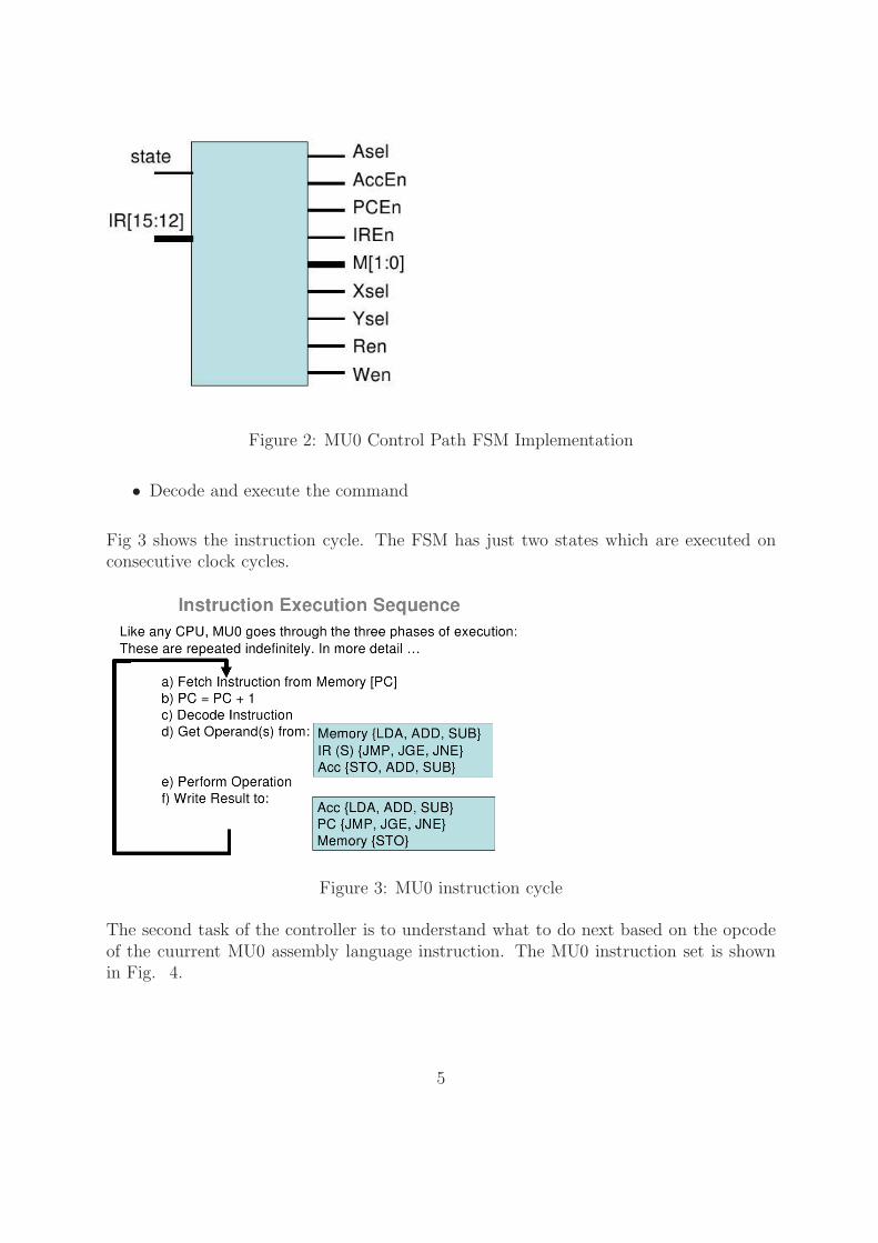
Figure 2: MU0 Control Path FSM Implementation
• Decode and execute the command
Fig 3 shows the instruction cycle. The FSM has just two states which are executed onconsecutive clock cycles.
Figure 3: MU0 instruction cycle
The second task of the controller is to understand what to do next based on the opcodeof the cuurrent MU0 assembly language instruction. The MU0 instruction set is shownin Fig. 4.
5

Figure 4: MU0 assembly language instructions
1.3 MU0 Operation
The first thing to do is to understand what goes on with these instructions. Note thesyntax of the commands. The symbol S refers to a memory address. The notation [S]refers to the contents stored at memory addressed.
Consider the datapath of Fig. 1. It shows the following hardware systems,
1. A program counter register (PC) which stores the address in the memory of thecurrent instruction. Exactly what is the current instruction and what is the nextinstruction we’ll see in a minute. The addresses count from 0 upwards and in anyprogram, the instructions are stored in the first contiguous memory locations whilethe data is store in the subsequent locations. This is the basis of the Von Neumannarchitecture wherein program and data are stored sequentially in memory.
2. An instruction register (IR) which contains the instruction while it is being exe-cuted.
3. An accumulator (ACC) which provides intermediate storage of data during in-struction execution. The ACC is sometimes referred to as the working register.
4. An Arithmetic Logic Unit (ALU)
5. Several multiplexers
6

In MU0 the data has 16 bits and the memory has storage locations that are 16 bits wide.The data in memory is stored at locations that can be located by their address. Theseaddresses are represented by words that are 12 bits wide. That is MU0’s memory has 212
memory locations where data can be stored.
It is interesting and entirely pertinent to note that an instruction word consistsof 16 bits and can therefore be stored in memory. The most significant four bits([15:12] in VERILOG parlance) of the instruction word is referred to as the opcode. Thisis the machine language symbol that represents an instruction. This is the hex numberF in the left most column of Fig. 4. There are 16 possible opcodes but only 8 areimplemented in MU0. The meanings of the instructions are also described in Fig. 4. Theremaining 12 bits in the instruction word is the address in memory of either the operandthat the instruction operates on (in the case of LDA, ADD and SUB) or the destinationof the data in the ACC (STO) or the address of the next instruction in the case of theJUMP commands (JMP, JGE, JNE).
Fig. 5 shows the instruction word format.
Figure 5: MU0 instruction format.
The program counter is incremented every instruction. It is only controlled by the activeedges of the clock. Consequently MU0 automatically runs sequentially through the ad-dresses in memory. Reading an instuction occurs when that instruction appears in the IRin the EXEC state.
The cunning in the design of the MU0 architecture is that each hardware block in thedatapath of Fig 1 is configured to execute these instructions by appropriate changes intheir control inputs. This is our standard model of a datapath. Examples of controlsare PCen (enable PC), ACCen (enable the ACC), Asel (choose the input thatconnects to the output of the address MUX, a-mux), M (choose the functionto be performed by the ALU), etc. The bit values of these controls are the outputsof the control path FSM.
1.3.1 The Control Path Finite State Machine
The next state diagram of the controller in Fig. 6 describes how the FSM works. Thefirst column shows the states of which there are just two,
0 FETCH (fetch instruction and store instruction in IR) and,
1 EXEC (decode instruction in the IR and execute instruction).
7

The second column shows the opcode, F. The opcode is MU0’s only input. MU0 obtainsthe opcode when the controller FSM reads bits [15:12] of the IR. The third column isthe next state that the controller jumps to. Note that the opcode is not needed in theFETCH state (0) because in this state the only steps are to mux the PC contents ontothe address bus through the a-mux and to set up the ALU input control, M, for a PCincrement. As a result, regardless of the F or opcode value, the next state is EXEC (1).This explains the dont cares, “XXX” in the F cell in the table.
Figure 6: MU0 next state diagram
If you look at the next-state diagram you should be able to confirm the interconnects ofMU0 in Fig. 7 for the FETCH state. The grey tracks indicate connected paths in thedatapath.
1.3.2 MU0 in action
Try and follow the following verbal description. Remember that all registers (PC, IR andACC) and state transitions occur on the positive edge of the clock but memory read andwrites occur on negative clock transitions.
The sequence of events that occur in the FETCH state from the first positive transitionof the system clock are as follows.
8

1. The FETCH cycle occurs at the first positive edge of the clock.
2. In the FETCH state the a-mux input is connected to the PC output. The MUX isa combinational device and so the PC contents should already be pointing to theaddress of the next instruction in memory.
3. At tbe ensuing negative clock transition the memory transfers the contents of thelocation whose address is in the PC to the Dbus. The Dbus is the output data lineof the memory whereas the Xbus is the input data line.
4. The contents of the Dbus are now present at the input to the IR.
5. In the FETCH state the PC contents are also pointing at the ALU input throughthe x-mux. The ALU M-value is set so that the ALU increments the value onthis input. Since both the x-mux and the ALU are combinational devices, the PCincremented contents are transferred instantaneously at the PC input. On the nextpositive clock transition the contents of the PC will be incremented ready for thenext time the FSM is in the FETCH state.
From the second positive clock transition we are in the EXEC state. The sequence ofevents that occur in the this state are as follows.
1. At this transition the PC increments its contents as discussed previously.
2. The IR registers the contents of the Dbus to its output.
3. The controller reads the [15:12] bits (the opcode) from the IR.
4. Depending on the opcode value, several function controls in the datapath may beenabled or disabled as follows.
• If the opcode is LDA then the ACC is enabled and the y-mux is set so thatthe Dbus is connected to the ALU input on the Ybus. The ALU M value is setfor a through connnection on its Ybus input. At the positive edge of the nextclock transition into the FETCH state, the ACC output will store the contentsof the Dbus.
• If the opcode is for ADD or SUB then the ACC is enabled and the Dbus isagain connected to the ALU via the Ybus through y-mux. The x-mux is set toallow the contents of the ACC onto the Xbus and the ACC M value is set forADD or SUB. On the subsequent negative clock transition the contents of thememory is transferred onto the Dbus. At the positive edge of the next clocktransition into the FETCH state, the ACC output will store the sum of itsprevious value and that in the memory location.
9

• If the opcode is STO, the x-mux places the contents of the ACC on the inputto the Xbus which is also the memory input data line. The last 12 bits of thecontents of the IR are sent via the a-mux to the address bus of the memory.On the next negative clock transition the memory stores the contents of theXbus (the contents of the ACC).
• In the case of the JUMP instructions, the last 12 bits of the instruction registerare sent via the y-mux to the Ybus and the ALU. The ALU is set for straightthrough so that this new memory address is fed to the PC. At the ensuingposedge of clock (FETCH) the PC is changed to the address which is theoperand of the JUMP instruction.
Figure 7: The MU0 datapath interconnects during FETCH and EXEC.
1.3.3 Running a Program on MU0
The following is a machine code listing of a MU0 program which adds the contents (000A)of memory location 4 to the contents (0001) of memory location 5. The first column con-sists of the addresses in memory in hex format. The second column contains the contentsof the memory locations which are the machine language commands to be executed.The first hex digit (most significant 4 bits) in each command is the opcode. These are0 (LDA), 2 (ADD), 1 (STO). The remaining 3 hex digits are the address operands asdiscussed above.
0 0004 (load (LDA) the contents of memory adddress 4 into the ACC)
1 2005 (add (ADD) the contents of memory address 5 to that in the ACC)
10

2 1006 (store (STO) the contents of the ACC in memory location 6)
3 7000 (STOP)
4 000A (data stored in memory location 4)
5 0001 (data stored in memory location 5)
6 0000 (data stored in memory location 6)
Notice how execution occurs in purely sequential fashion. MU0 does not know whichmemory addresses contain instructions and which data. Its proper operation dependsentirely on proper programming and the march of the PC contents. The STOP commandterminates execution and prevents the processor from trying to perform a false opcode inthe first hex digit of the data at memory location 4.
Notice that for simulation a memory controller has been used that reads the file prog.lst
from the disk which contains the machine language commands.
Fig 8 shows the complete GTKWAVE output from running MU0 with ICARUS VER-ILOG.
Figure 8: GTKWAVE traces of the MU0 data during execution of the above program
11

Fig. 9 expands the traces around the FETCH and EXEC states when the instruction2005 is being executed. For instruction 2005 the PC is pointing to address 1 in memory.During this instruction the contents of memory address 5 (0001) is added to the contentsof the accumulator which is by now 000A. Notice that the actual instruction 2005 doesnot appear in the IR until the EXEC state is reached and that the contents of the ACCdo not register the sum, 000B, until the FETCH cycle of the following instruction.
PC
IR
ACC
CLOCK
0001
2005 20051004
0001 0001 0002 0002
0000 000A 000A 000A 000B000A
1004 1004
FETCH EXEC FETCH
2005
0002
Figure 9: Expected and GTKWAVE traces of MU0 ACC, IR and PC registers aroundthe execution of the 2005 instruction
Exercise 2: Run MU0 for the above program (stored in proh.lst) and try tounderstand the outputs.
1.3.4 MU0 Assembly Language?
The lexical commands in Fig. 4, LDA, STO, etc are referred to as assembly languageinstructions. Normally when writing programs for a microprocessor one only has to usethese commands and some variables representing the data. This is clearly much easier toread than the column of numbers that form the machine code. However use of assemblylanguage presumes the existence of an assembly language compiler or assembler for shortwhich translates tbe assembly language into machine code. Unfortunately (to the bestof my knowledge) MU0 does not have an assembler written for it (though you may beattempted to write one in JAVA or C, I dont think it would be difficult).
1.4 Programming Exercises
In this section we are go get some practice writing MU0 programs.
Exercise 3. Describe the function of the following MU0 program. (Be carefulthat there are enough time steps available in the simulation to complete theexecution of the progam.
12

0006
3007
1006
0006
5000
7000
0004
0001
Exercise 4. Write a MU0 to add the numbers from 1 - 5.
13
Related Documents