1 ENGINEERING HIGHLY ORGANIZED AND ALIGNED SINGLE WALLED CARBON NANOTUBE NETWORKS FOR ELECTRONIC DEVICE APPLICATIONS: INTERCONNECTS, CHEMICAL SENSOR, AND OPTOELECTRONICS A dissertation presented by Young Lae Kim to The Department of Electrical and Computer Engineering In partial fulfillment of the requirements for the degree of Doctor of Philosophy in the field of Electrical Engineering Northeastern University Boston, Massachusetts May, 2013

Welcome message from author
This document is posted to help you gain knowledge. Please leave a comment to let me know what you think about it! Share it to your friends and learn new things together.
Transcript
1
ENGINEERING HIGHLY ORGANIZED AND ALIGNED SINGLE WALLED CARBON
NANOTUBE NETWORKS FOR ELECTRONIC DEVICE APPLICATIONS:
INTERCONNECTS, CHEMICAL SENSOR, AND OPTOELECTRONICS
A dissertation presented
by
Young Lae Kim
to
The Department of Electrical and Computer Engineering
In partial fulfillment of the requirements for the degree of
Doctor of Philosophy
in the field of
Electrical Engineering
Northeastern University
Boston, Massachusetts
May, 2013

2
ENGINEERING HIGHLY ORGANIZED AND ALIGNED SINGLE WALLED CARBON
NANOTUBE NETWORKS FOR ELECTRONIC DEVICE APPLICATIONS:
INTERCONNECTS, CHEMICAL SENSOR, AND OPTOELECTRONICS
by
Young Lae Kim
ABSTRACT OF DISSERTATION
Submitted in partial fulfillment of the requirements
for the degree of Doctor of Philosophy in Electrical Engineering
in the Graduate School of Engineering of
Northeastern University
May, 2013

3
Abstract
For 20 years, single walled carbon nanotubes (SWNTs) have been studied actively due to their
unique one-dimensional nanostructure and superior electrical, thermal, and mechanical
properties. For these reasons, they offer the potential to serve as building blocks for future
electronic devices such as field effect transistors (FETs), electromechanical devices, and various
sensors. In order to realize these applications, it is crucial to develop a simple, scalable, and
reliable nanomanufacturing process that controllably places aligned SWNTs in desired locations,
orientations, and dimensions. Also electronic properties (semiconducting/metallic) of SWNTs
and their organized networks must be controlled for the desired performance of devices and
systems. These fundamental challenges are significantly limiting the use of SWNTs for future
electronic device applications. Here, we demonstrate a strategy to fabricate highly controlled
micro/nanoscale SWNT network structures and present the related assembly mechanism to
engineer the SWNT network topology and its electrical transport properties. A method designed
to evaluate the electrical reliability of such nano- and microscale SWNT networks is also
presented. Moreover, we develop and investigate a robust SWNT based multifunctional selective
chemical sensor and a range of multifunctional optoelectronic switches, photo-transistors,
optoelectronic logic gates and complex optoelectronic digital circuits.

4
Acknowledgement
I would really like to express my deepest appreciation to many people who gave me the
continuing help and support to complete the work. Especially, I would like to thank my thesis
advisor, Professor Yung Joon Jung for his continued support and guidance and Professor Swastik
Kar for his grateful advice. This is a really grateful opportunity they gave me to learn and work
under their supervision. Moreover, I appreciate not only his research advices but also his
personal advices for life. I give thanks to Professor Busnaina who supported the work. I am
indebted to Professors Nian Sun and Professor Hossein Mosallaei in Electrical and Computer
department for their advices. I also give thanks to Dr. Robert Keller, Dr. Mark Strus, and Dr.
Ann Chiaramonti Debay who are my collaborators at National Institute of Standards and
Technology (NIST). I also would like to thank my laboratory colleagues, Dr. Hyun Young Jung,
Dr. Myung Gwan Hahm, Hyunkyung Chun, Dr. Bo Li, Sanghyun Hong, Ji Hao, and A Mi Yu
for everything they helped and supported me. In addition, I wish to thank my colleagues, Mr.
Fangze Liu and Dr. Xiaohong An in Physics department and the members of the Center for
High-rate Nano-manufacturing (CHN), Dr. Jin Young Lee (CHN), Han Chul Cho (CHN), Jung
Ho Seo (CHN), and Dr. Geun Ho Cho (ECE), Dr. Dong-Woo Seo (Civil Engineering) at
Northeastern University for helping me during my study.
I would like to give thanks to Professor Bo Hyun Wang (M.S. thesis advisor), Professor
Myung Seok Cho, Professor Yoon Tae Jung, Professor Sang Min Lee, Professor Byung Gwan
Im, Professor Rae Jung Park, Professor Deok Soo Joen, Professor Moon Sik Gang, and Professor
Jung Ho Moon at Kangnung National University in Republic of Korea for their advice during
studying in U.S. I also want thank to my best friends, Ki Yoon Hong, Sang Soo Lee, Ho Sang
Son, Yong Chul Jung, Jong Gil Choi, Jin Yong Park, Geun Woo Park, Beom Soo Jang, Hyeok

5
Goo Kwon, Hwan Soon Yoo, and Ho Sung Kim who have supported me many great things.
Especially, I really appreciate it for the continuing support from my family. I would really like
to give my special thanks to in memory of my father, Nam Ho Kim, and my mother, San Gyu
Kim, for their never ending belief and love. I am also grateful to my brothers Kyung Rae Kim,
Wan Rae Kim, and their wives Geom Soon Hahm, Mal Nyeo Min, and to my sisters, Geom Soon
Kim, Na Kyung Kim, and Geom Joo Kim, and their husbands Jae Hak Oh, in memory of Ja
Deok Yang, and Young Han Lee who gave me continuing support and helps to complete this
work. I also appreciate it for the continuing understanding and support from my wife’s family. I
would really like to give my special thanks to my parents-in-law, Hong Seong Kim and Kyung
Ja Chae, and its family Hong Aeon Kim and Yoo Deok Kim, Myung Soo Kang and Jeong Geom
Kim, Hee Jong Kim and Nan Joon Park, Mi Ye Kim, Myung Jong Kim and Si Yeon Jeon,
Young Ah Kang and Young Na Kang.
I would like to especially thank to my wife, Mi Hun Kim, who really understands, supports,
and guides me to complete my Ph.D. degree from outside our hometown in Korea. I would like
to express my true love to my lovely daughters, Christina (Siyul) Kim and Olivia (Hayul) Kim.

6
Table of Contents
Abstract ........................................................................................................................................... 3
Acknowledgement .......................................................................................................................... 4
Table of Contents ............................................................................................................................ 6
List of Figures ................................................................................................................................. 9
Introduction ................................................................................................................................... 12
Chapter 1: Single Walled Carbon Nanotubes ............................................................................... 15
1.1 Structure of Single Walled Carbon Nanotubes ................................................................... 15
1.2 Electrical Properties of Single Walled Carbon Nanotubes ................................................. 18
1.3 Optical Properties of Single Walled Carbon Nanotubes ..................................................... 21
1.4 Fabrication of Highly Organized SWNT Networks ............................................................ 23
1.5 Assembly Mechanism of Highly Organized SWNT Networks .......................................... 26
1.6 Topological Transitions in CNT Networks via Nanoscale Confinement ........................... 29
Chapter 2: Metallization of SWNT Network for Interconnect Applications ............................... 34
2.1 Introduction ......................................................................................................................... 34
2.2 Fabrication of Highly Aligned SWNT Lateral Architectures ............................................. 36
2.3 Detailed Study of the Alignment of SWNT Architectures ................................................. 36
2.4 Electrical Properties of SWNT Architectures before Metallization.................................... 39
2.5 ab-initio Density Functional Theory Calculations .............................................................. 41
2.6 Pt Decoration of SWNT Architectures................................................................................ 44
2.7 Electrical Properties of Highly Aligned SWNT Structures after Pt Decoration ................. 46
2.8 Calculation of Resistance before and after Pt Decoration................................................... 51
2.9 Conclusions ......................................................................................................................... 54
7
Chapter 3: Reducing Interfacial Contact Resistance of Organized SWNT Interconnect Structures
....................................................................................................................................................... 56
3.1 Introduction ......................................................................................................................... 56
3.2 Fabrication of Organized SWNT Interconnect Structures .................................................. 58
3.3 Measurement of Contact Resistance ................................................................................... 58
3.4 Purification Methods for Contact Area between SWNTs and Contact Electrode .............. 62
3.5 Contact Resistance depending on Purification Methods ..................................................... 65
3.6 Dependence of Contact Resistance on Temperature ........................................................... 70
3.7 Conclusions ......................................................................................................................... 70
Chapter 4: Chemical Sensor Based on Highly Organized SWNT Networks for Hydrogen Sulfide
....................................................................................................................................................... 73
4.1 Introduction ......................................................................................................................... 73
4.2 Fabrication of SWNT Networks for Sensors ...................................................................... 74
4.3 Non-covalent Functionalization of SWNTs ........................................................................ 75
4.3.1 Functionalization of SWNTs with Nitroxyl Radical Based Compounds ..................... 77
4.4 Hydrogen Sulfide Gas Detection of SWNT Networks ....................................................... 77
4.4.1 Detection of Hydrogen Sulfide in Air .......................................................................... 78
4.4.2 Detection of Hydrogen Sulfide with Metallic/Semiconducting SWNTs in condition of
Water Vapor .......................................................................................................................... 81
4.5 Conclusions ......................................................................................................................... 87
Chapter 5: Optoelectronic Properties of Heterojunction between SWNTs and Silicon ............... 89
5.1 Introduction ......................................................................................................................... 89
5.2 Literature Review ................................................................................................................ 91
5.2.1 Conventional Photodetectors ........................................................................................ 91
5.2.2 Optoelectronic Photoswitches ...................................................................................... 92
5.2.3 Carbon Nanotubes and CNT-Si Heterojunction based Photo-devices ......................... 92

8
5.3 Optoelectronic Properties of SWNT-Si Hetrojunction ....................................................... 94
5.4 A Very-large Scale Sensor Array of SWNT-Si Hetrojunction ......................................... 100
5.5 Optoelectronic Logic Devices based on SWNT-Si Hetrojunction.................................... 102
5.6 Conclusions ....................................................................................................................... 106
Conclusions ................................................................................................................................. 107
Appendix A ................................................................................................................................. 110
Appendix B ................................................................................................................................. 116
Bibliography ............................................................................................................................... 122

9
List of Figures
Figure 1. Honeycomb lattice of a nanotube. H. Dai, Accounts of chemical research, 2002 [10].16
Figure 2. Electronic structure of graphene calculated within a tight-binding model consisting
only of electrons. M. Anantram et al., Reports on Progress in Physics [12]. ....................... 19
Figure 3. Schematic of Brillouin zone of a single graphene sheet J. Bernholc, et al., Annual
Review of Materials Research,2002 [14]. ............................................................................. 20
Figure 4. DoS and optical excitations of SWNT. H. Kataura et al, Synthetic Metals, 1999. ...... 22
Figure 6. Contact angle measurements. L. Jaber-Ansari, et al, JACS, 2008 [34]. ....................... 27
Figure 7. Effect of plasma treatment on the surface morphology of Si. L. Jaber-Ansari, et al,
JACS, 2008 [34]. .................................................................................................................... 28
Figure 9. Schematic and SEM images showing super-aligned SWNT interconnect structures. . 37
Figure 10. Polarized Raman spectra from SWNT arrays. ............................................................ 38
Figure 11. Electrical characteristization of aligned SWNT interconnect structures. ................... 40
Figure 12. Calculations of the effect of Pt-decoration on electronic properties of SWNTs. ....... 43
Figure 13. Pt-decoration on SWNTs and its characterization. ..................................................... 45
Figure 14. Electrical properties of SWNT structures before and after Pt decoration. ................. 48
Figure 15. Comparison between predicted and experimentally measured resistance ratio of Pt-
decorated and pristine test structures. .................................................................................... 53
Figure 16. SEM images of a highly organized SWNT structure. ................................................ 59
Figure 17. Measurement of contact resistance in SWNT architectures. ...................................... 61
Figure 18. Purification processes of highly organized SWNTs. .................................................. 64
Figure 19. Electrical properties and SEM images of SWNT structures depending on the
treatment of cleaning. ............................................................................................................ 67
Figure 20. Percentage of contact resistance in overall resistance, showing the contact resistances
are decreased according to the different cleaning process. ................................................... 69
Figure 21. Change of contact resistance depending on temperatures. ......................................... 71

10
Figure 22. SEM images of SWNT-based devices with wire bonding. ........................................ 76
Figure 23. Shown schematically is the definition of the “Response Time” for an electrical sensor.
............................................................................................................................................... 79
Figure 24. Glass chamber setup for controlled environment measurements. .............................. 79
Figure 25. Current vs. time plot monitored for different concentrations of H2S gas. .................. 80
Figure 26. Shown is a plot of Response time vs Concentration of H2S gas clearly revealing the
working range and saturation region for the functionalized SWNT sensor. ......................... 81
Figure 27. Device schematic and the behavior of H2S and H2O molecules on SWNTs
functionalized by TEMPO. .................................................................................................... 83
Figure 28. Sensitivity and real-time current measurements for detection of H2S gas. ................ 84
Figure 29. Schematic of redox reactions of H2S on p-doped CNT (due to, for example, O2
adsorption) with TEMPO functionalization in the presence of H2O. .................................... 86
Figure 30. SWNT/Si heterojunction structure and photoresponses. ............................................ 96
Figure 31. Large scale sensor array and photocurrent map. ...................................................... 101
Figure 32. Phototransistor and AND gate based on SWNT/Si heterojunction. ......................... 103
Figure 33. ADDER and 4-BIT optoelectronic D/A converter based on SWNT/Si heterojunction.
............................................................................................................................................. 104
Figure 34. Real time current changes of bare s-SWNT device exposed to H2S gas of 5, 10, 50,
100, and 200 ppm in dry N2. ................................................................................................ 111
Figure 35. The sensitivity of a bare m-SWNT device as function of the H2S concentrations in
dry N2. ................................................................................................................................. 111
Figure 36. Real-time current measurement of a bare s-SWNT device as a function of RH. The
current reaches almost its saturation value. ......................................................................... 112
Figure 37. A bare m-SWNT device test with H2O vapor and H2S gas. ..................................... 113
Figure 39. Real-time current measurement of s-SWNT device functionalized with TEMPO as a
function of RH. The current reaches almost its saturation value. ........................................ 114
Figure 40. A bare m-SWNT functionalized device test with H2O vapor and H2S gas. ............. 115
Figure 41. Optical properties in heterojunction between SWNTs and Si. ................................. 117

11
Figure 42. Optical and SEM images of a very-large scale sensor array. ................................... 119
Figure 43. Optical images of assembled SWNTs and electrodes. ............................................. 120
Figure 44. Tested sensor array images for a Raman mapping measurement. ............................ 120
Figure 45. G-band intensities using a Raman mapping process corresponding to 2 by 2 sensor
array. .................................................................................................................................... 121

12
Introduction
Since the discovery of single walled carbon nanotubes (SWNTs) in the early 1990s [1, 2],
there has been intense activity exploring the electrical properties of these systems and their
potential applications in electronics. SWNT is a graphene roll with a diameter of 0.5 to a few
nanometers that can be either metallic or semiconducting depending on its chirality. However,
multi walled carbon nanotubes (MWNTs) are concentric graphene tubes that can have diameters
typically from 2 nm to 25 nm. The unique properties of carbon nanotubes (CNTs) can be
attributed to the one-dimensional nature of nanotubes, the strong sp2 carbon bonds, and the
peculiar band-structure of graphene. The sp2 bonding in graphene is even stronger than the sp
3
bonding in diamond [3], and therefore CNTs have very high mechanical strengths. The
combination of high degree of crystalline order with very less defects, large mechanical strength
and the relatively small interaction between electrons and carbon atoms enables CNTs to conduct
very large current densities of 109 A·cm
-2 [4].
In chapter 1, the electronic structure and properties of SWNTs were discussed for
understanding basic physics of them. This chapter also discussed a fabrication method and
transition for SWNT networks. The many possible symmetries or geometries that can be realized
on a cylindrical surface in SWNTs without the introduction of strain are the importance to
carbon nanotube physics. For one-dimensional (1D) system on a cylindrical surface, translational
symmetry with a screw axis could affect the electronic structure and related properties. With
understanding the basic physics of SWNTs, this chapter focuses on the structure, electrical
properties, and optical properties of SWNTs. Then, this chapter introduced a fabrication method
for micro-to-nano scale patterned SWNT networks using a newly developed template guided
fluidic assembly process. A mechanism for SWNT assembly and their control was described

13
here. To maximize the directed assembly efficiency of SWNTs toward a wafer level SWNT
deposition, Si or SiO2 substrate was pretreated with precisely controlled plasma treatment.
Chemical and physical properties of the surface were characterized using several surface
characterization techniques to investigate and control the mechanism of SWNT assembly. Last,
this chapter demonstrated the effectiveness of directed assembly on channels with varying
degrees of confinement as a simple tool to tailor the conductance of the otherwise heterogeneous
network, opening up the possibility of robust large-scale carbon nanotube networks (CNN)-based
devices.
In chapter 2, the fabrication and characterization of nanoscale electrical interconnect test
structures constructed from aligned single walled carbon nanotubes using a template-based
fluidic assembly process were presented. These structures can withstand current densities ~ 107
Acm-2
, comparable or better than copper at similar dimensions. In addition, we present a novel
Pt-nanocluster decoration method that drastically decreases the resistivity of the test structures.
Ab-initio density functional theory calculations indicate that the increase in conductivity of the
nanotubes is caused by an increase in conduction channels close to their Fermi levels due to the
platinum nanocluster decoration, with a possible conversion of the semiconducting single walled
carbon nanotubes into metallic ones.
In chapter 3, a method is presented for significantly reducing the interfacial contact resistance
of SWNT interconnect test-structures. Conventional lithographic cleaning steps are insufficient
for complete removal of lithographic residues in SWNT networks, leading to large interfacial
contact resistance. Using improved purification procedures and controlled developing time, the
interfacial contact resistance between SWNTs and contact electrodes of Ti/Au were found to

14
reach values below 2% of the overall resistance in two-probe test-structures of SWNTs,
demonstrating the importance of cleaning lithographic residues from the surface of SWNTs
before the fabrication of metal electrodes.
In chapter 4, the effective detection of hydrogen sulfide gas by a redox reaction based on
SWNTs functionalized with TEMPO as a catalyst was introduced and we also discuss the
important role of water vapor on the electrical conductivity of SWNTs during the sensing of H2S
molecules. To explore the H2S sensing mechanism, we investigate the adsorption properties of
H2S on CNTs and the effects of the TEMPO functionalization and we summarize current
changes of devices resulting from the redox reactions in the presence of H2S.
Chapter 5 introduced a radically unconventional, voltage-tunable, sharply non-linear and
extremely sensitive photo-response in fludically-assembled single walled carbon nanotube/Si
heterojunctions, with high photocurrent responsivity, high photovoltage responsivity, high
electrical ON/OFF ratios and optical ON/OFF ratios. The large scale optoelectronic sensor was
demonstrated by fabricating an array of 250,000 micron-scale photo-active junctions covering a
centimeter-scale wafer. We also presented bidirectional phototransistors, and novel logic
elements such as a mixed optoelectronic AND gate, a 2-Bit optoelectronic ADDER/OR gate, and
a 4-Bit optoelectronic D/A converter.

15
Chapter 1: Single Walled Carbon Nanotubes
The many possible symmetries or geometries that can be realized on a cylindrical surface in
SWNTs without the introduction of strain are the importance to carbon nanotube physics. For
one-dimensional (1D) system on a cylindrical surface, translational symmetry with a screw axis
could affect the electronic structure and related properties [5]. With understanding the basic
physics of SWNTs, this chapter focuses on the structure, electrical properties, and optical
properties of SWNTs.
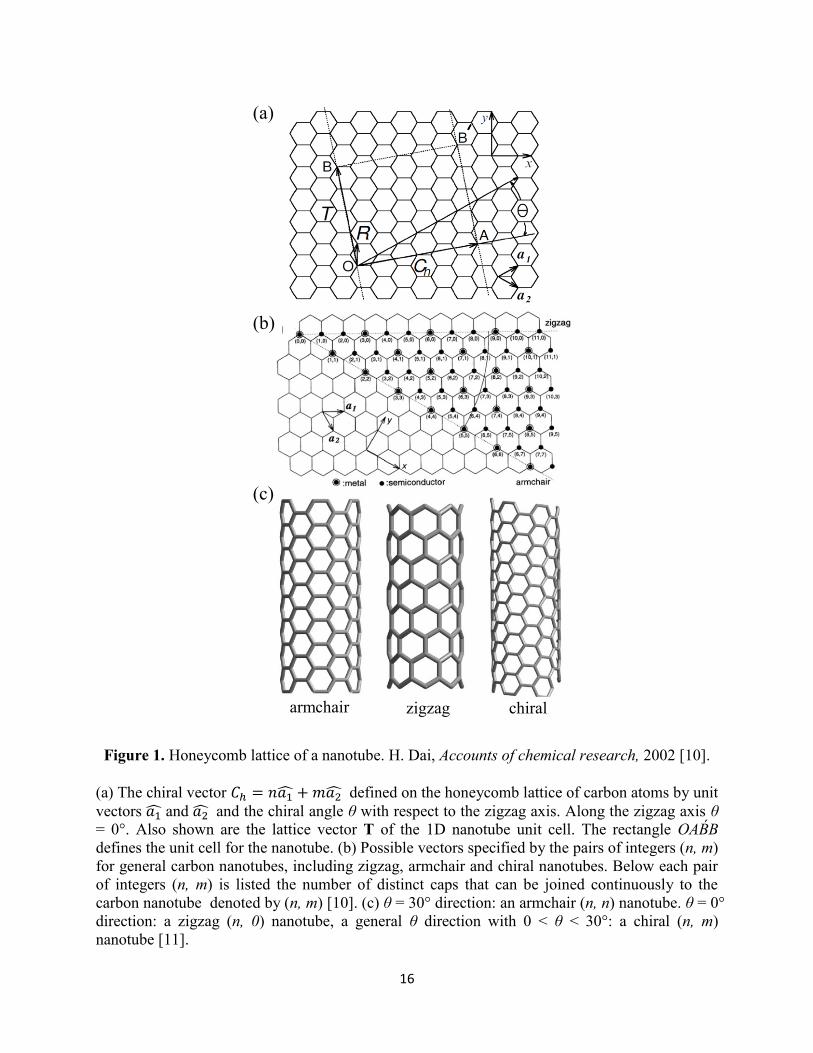
1.1 Structure of Single Walled Carbon Nanotubes
In the theoretical carbon nanotube structure, single walled tubes are focused, cylindrical in
shape with caps at each end, such that a fullerene can be formed with the two caps. The
cylindrical portions of the tubes consist of a single graphene sheet which is formed the cylinder.
With the discovery of SWNTs [6, 7], it is possible to investigate the predictions of the theoretical
calculations [5]. It is convenient to specify a general carbon nanotube in terms of the tube
diameter d, and the chiral angle θ, which are shown in Figure 1(a). The chiral vector Ch is
defined as
( ) (1.1)
which is often described by the pair of indices (n, m) that denoted the number of unit vectors
and in the hexagonal honeycomb lattice contained in the vector Ch [8]. The vector Ch
connected two crystallographically equivalent sites O and A on a two dimensional graphene
sheet where carbon atom is located at each vertex of the honeycomb structure [9]. The chiral
16
Figure 1. Honeycomb lattice of a nanotube. H. Dai, Accounts of chemical research, 2002 [10].
(a) The chiral vector defined on the honeycomb lattice of carbon atoms by unit
vectors and and the chiral angle θ with respect to the zigzag axis. Along the zigzag axis θ
= 0°. Also shown are the lattice vector T of the 1D nanotube unit cell. The rectangle
defines the unit cell for the nanotube. (b) Possible vectors specified by the pairs of integers (n, m)
for general carbon nanotubes, including zigzag, armchair and chiral nanotubes. Below each pair
of integers (n, m) is listed the number of distinct caps that can be joined continuously to the
carbon nanotube denoted by (n, m) [10]. (c) θ = 30° direction: an armchair (n, n) nanotube. θ = 0°
direction: a zigzag (n, 0) nanotube, a general θ direction with 0 < θ < 30°: a chiral (n, m)
nanotube [11].
armchair zigzag chiral
(a)
(b)
(c)
17
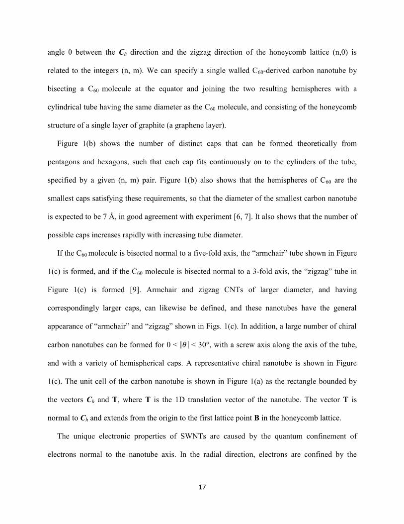
angle θ between the Ch direction and the zigzag direction of the honeycomb lattice (n,0) is
related to the integers (n, m). We can specify a single walled C60-derived carbon nanotube by
bisecting a C60 molecule at the equator and joining the two resulting hemispheres with a
cylindrical tube having the same diameter as the C60 molecule, and consisting of the honeycomb
structure of a single layer of graphite (a graphene layer).
Figure 1(b) shows the number of distinct caps that can be formed theoretically from
pentagons and hexagons, such that each cap fits continuously on to the cylinders of the tube,
specified by a given (n, m) pair. Figure 1(b) also shows that the hemispheres of C60 are the
smallest caps satisfying these requirements, so that the diameter of the smallest carbon nanotube
is expected to be 7 Å, in good agreement with experiment [6, 7]. It also shows that the number of
possible caps increases rapidly with increasing tube diameter.
If the C60 molecule is bisected normal to a five-fold axis, the “armchair” tube shown in Figure
1(c) is formed, and if the C60 molecule is bisected normal to a 3-fold axis, the “zigzag” tube in
Figure 1(c) is formed [9]. Armchair and zigzag CNTs of larger diameter, and having
correspondingly larger caps, can likewise be defined, and these nanotubes have the general
appearance of “armchair” and “zigzag” shown in Figs. 1(c). In addition, a large number of chiral
carbon nanotubes can be formed for 0 < | | < 30°, with a screw axis along the axis of the tube,
and with a variety of hemispherical caps. A representative chiral nanotube is shown in Figure
1(c). The unit cell of the carbon nanotube is shown in Figure 1(a) as the rectangle bounded by
the vectors Ch and T, where T is the 1D translation vector of the nanotube. The vector T is
normal to Ch and extends from the origin to the first lattice point B in the honeycomb lattice.
The unique electronic properties of SWNTs are caused by the quantum confinement of
electrons normal to the nanotube axis. In the radial direction, electrons are confined by the

18
monolayer thickness of the graphene sheet. Consequently, electrons can propagate only along the
nanotube axis, and so to their wave vector points. It is extraordinary that SWNTs can be either
metallic or semiconducting depending on the choice of (m, n), although there is no difference in
the chemical bonding between the carbon atoms within the nanotube and no doping or impurities
are present.
1.2 Electrical Properties of Single Walled Carbon Nanotubes
Each carbon atom in the hexagonal lattice possesses six electrons and carbon has two 1s
electrons, three 2sp2 electrons and one 2p electron in the graphite structure. The three 2sp
2
electrons form the three bonds in the plane of the graphene sheet, leaving an unsaturated π orbital
[3]. This π orbital, which is perpendicular to the graphene sheet and the nanotube surface, forms
a delocalized π network across the nanotube, which is responsible for its electronic properties. To
obtain the electronic structure of CNTs, we start from the bandstructure of graphene and quantize
the wavevector in the circumferential direction,
(1.2)
where C is shown in Figure 1(a) and p is an integer [12]. This equation provides a relation
between kx and ky defining lines in the (kx, ky) plane. Each line gives a one-dimensional energy
band by slicing the two-dimensional bandstructure of graphene shown in Figure 2. The particular
values of Cx, Cy and p determine where the lines intersect the graphene bandstructure, and thus
each CNT will have a different electronic structure. Perhaps the most important aspect of this
construction is that CNTs can be metallic or semiconducting, depending on whether or not the
lines pass through the graphene Fermi points. This concept is illustrated in Figure 3.

19
Figure 2. Electronic structure of graphene calculated within a tight-binding model consisting
only of electrons. M. Anantram et al., Reports on Progress in Physics [12].
Although graphene is a zero-gap semiconductor, SWNTs can have the electrical properties of
metals or semiconductors with different sized energy gaps, depending on their diameter and
chirality. The salient electronic properties of nanotubes may be understood in terms of a simple
tight-binding model [13]. For instance, consider an infinite graphene sheet. Carbon nanotubes are
formed when the graphene sheet is rolled up into a cylinder in such a way that the carbon atoms
connect seamlessly with each other. This implies that carbon atoms whose relative position
vector is Equation (1.1) must overlap, which in turn gives the condition k.C = q2π, where q is an
integer. This relation defines a set of parallel lines with a relative separation C/2π. Schematically,
these lines are represented for three types of nanotubes with helicity indices (n,m) (Figure 3).
The K point ( ( ) ) is the point where the π and bands of a graphene sheet meet,
defining the Fermi energy. Depending on whether a line intercepts or misses the K point, the

20
Figure 3. Schematic of Brillouin zone of a single graphene sheet. J. Bernholc, et al., Annual
Review of Materials Research,2002 [14].
The lines k.C = q2π are drawn for (a) an armchair (3,3), (b) a zigzag (3,0), and (c) a chiral (4,2)
nanotube. The K point of the Brillouin zone is the crossing point of the π and bands. The
nanotube will be metallic only if one of the lines intercepts this point. From the drawing, this
condition will only be met for certain orientations and spacing (~R-1
) of the set of lines. J.
resulting nanotube will be either metallic or semiconducting. Thus tubes for which (m - n) is
divisible by three will have a finite density of states at the Fermi level and will therefore be
metallic. In particular, all armchair n = m nanotubes are metallic, whereas only third of the m = 0
zigzag nanotubes have metallic characteristics.
Although this model is relatively simple, it works remarkably well. There are, however,
limitations that result from a possible mixing between the in-plane σ and out-of-plane π orbitals.
These orbitals are, of course, orthogonal for a simple graphene sheet but may be somewhat
mixed for highly curved systems. As a general rule, this mixing can be neglected for nanotubes
with radii greater than 10 Å. For nanotubes with radii in the range of 2.5 to 10 Å, a small band
gap decreasing with the second power of the radius appears in all but the armchair nanotubes.
(a) (b) (c)
21
For nanotubes with even smaller radii—some of which have been synthesized recently—the
simple model presented here is no longer valid, and more fundamental, first-principles
calculations are needed to adequately describe the electronic properties of these very-small-
diameter nanotube systems [15]. Furthermore, single walled nanotubes usually self-assemble in
bundles called ropes owing to van der Waals attraction. The intertube interactions introduce
small pseudogaps in ropes of nominally metallic tubes [16, 17].
1.3 Optical Properties of Single Walled Carbon Nanotubes
The optoelectronic properties of carbon nanotubes have gained much attention recently,
stimulated by their unique electronic structure [18-25]. Reports have revealed intriguing behavior
for nanotubes, which show a strong interaction between electrical transport and optical fields.
Typical examples include the use of aligned nanotube arrays as microwave amplifiers and radio
antennas [24, 25]. The nanotubes, when receiving the incident electromagnetic waves, generate
enhanced electrical signal due to their small dimension and sharp tips. The optical absorption and
emission from SWNTs cover a spectrum from the visible to the infrared range, which is
important for making optoelectronic devices [21-23]. Recently, the photoconductivity of
nanotubes has been studied theoretically in a nanotube p–n junction [20], a single SWNT
transistor [19], and thin SWNT films [18]. The photocurrent has a resonance-to-photon energy in
the range of 0.7 to 1.5 eV with peak positions corresponding to the bandgap of semiconducting
SWNTs, promising that nanotubes can act as photosensitive materials [26].
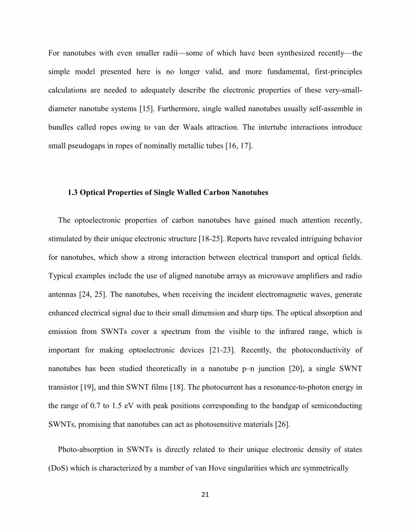
Photo-absorption in SWNTs is directly related to their unique electronic density of states
(DoS) which is characterized by a number of van Hove singularities which are symmetrically
22
Figure 4. DoS and optical excitations of SWNT. H. Kataura et al, Synthetic Metals, 1999.
(a-b) DoS and possible optical excitations in (a) a (8,8) metallic and (b) a (9,7) semiconducting
SWNT, both of which have a diameter of about 1.1 nm. (c) Variation of excitation energies with
diameter in the SWNT family.
distributed about its Fermi level [27]. As a result, photo-induced excitations in SWNTs occur not
only at the band-gap, but also between energy levels corresponding to electron-hole pair (Exciton)
formations between its mirror-symmetric van Hove singularities. Figure 4(a) and 4(b) shows the
1D DoS and its corresponding possible optical excitations in a metallic and a semiconducting
SWNT [28]. Depending on the chirality (m,n) and diameter, SWNTs can have a whole range of
possible optical excitations, as seen in figure 4(c). As an optical material, carbon nanotubes are
extremely unique, since nanotubes within a short diameter range can have vastly varying
possible optical excitations. In a bundle, rope, films or ribbon configurations, SWNTs hence
form a very unique nanoscale semiconductor material with a large number of Excitonic energy
levels.
23
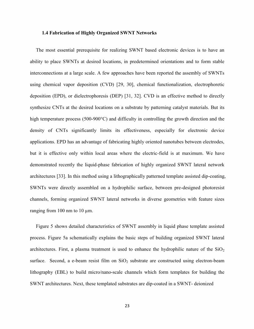
1.4 Fabrication of Highly Organized SWNT Networks
The most essential prerequisite for realizing SWNT based electronic devices is to have an
ability to place SWNTs at desired locations, in predetermined orientations and to form stable
interconnections at a large scale. A few approaches have been reported the assembly of SWNTs
using chemical vapor deposition (CVD) [29, 30], chemical functionalization, electrophoretic
deposition (EPD), or dielectrophoresis (DEP) [31, 32]. CVD is an effective method to directly
synthesize CNTs at the desired locations on a substrate by patterning catalyst materials. But its
high temperature process (500-900°C) and difficulty in controlling the growth direction and the
density of CNTs significantly limits its effectiveness, especially for electronic device
applications. EPD has an advantage of fabricating highly oriented nanotubes between electrodes,
but it is effective only within local areas where the electric-field is at maximum. We have
demonstrated recently the liquid-phase fabrication of highly organized SWNT lateral network
architectures [33]. In this method using a lithographically patterned template assisted dip-coating,
SWNTs were directly assembled on a hydrophilic surface, between pre-designed photoresist
channels, forming organized SWNT lateral networks in diverse geometries with feature sizes
ranging from 100 nm to 10 µm.
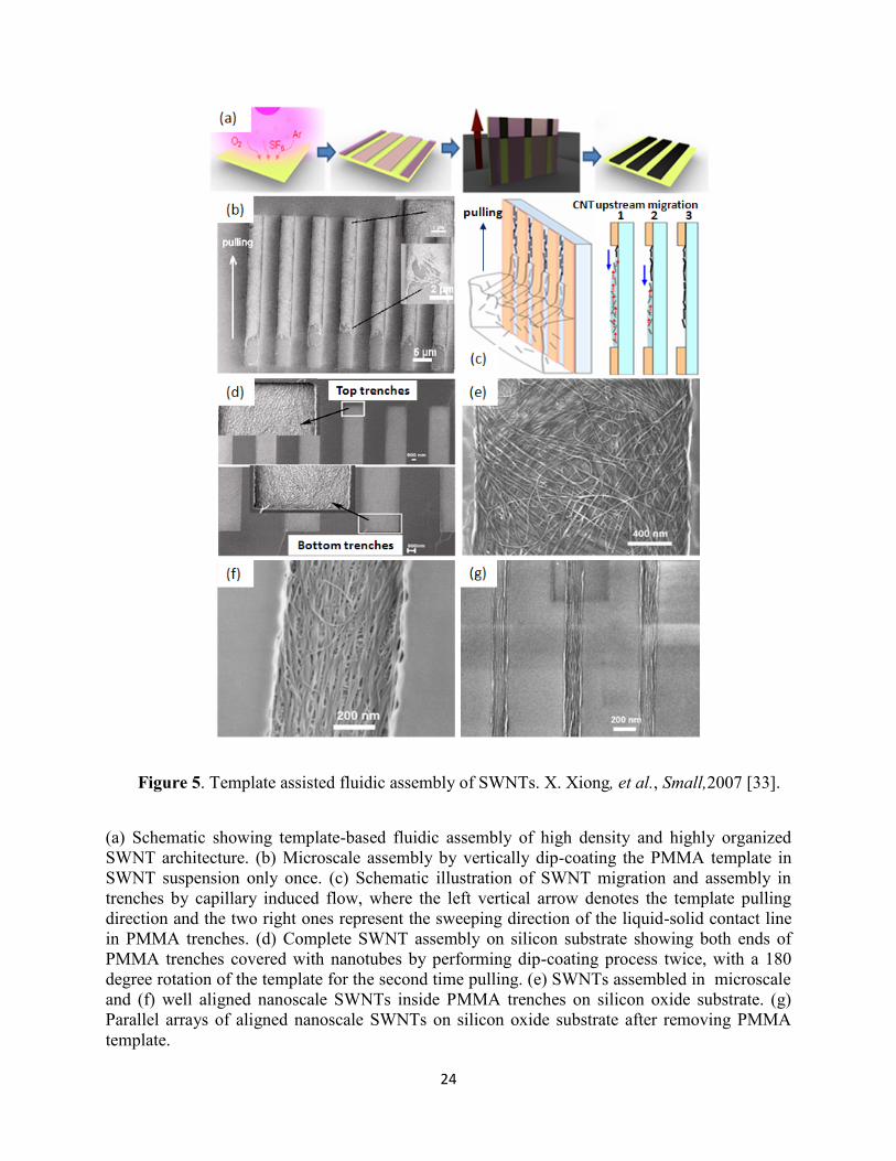
Figure 5 shows detailed characteristics of SWNT assembly in liquid phase template assisted
process. Figure 5a schematically explains the basic steps of building organized SWNT lateral
architectures. First, a plasma treatment is used to enhance the hydrophilic nature of the SiO2
surface. Second, a e-beam resist film on SiO2 substrate are constructed using electron-beam
lithography (EBL) to build micro/nano-scale channels which form templates for building the
SWNT architectures. Next, these templated substrates are dip-coated in a SWNT- deionized
24
Figure 5. Template assisted fluidic assembly of SWNTs. X. Xiong, et al., Small,2007 [33].
(a) Schematic showing template-based fluidic assembly of high density and highly organized
SWNT architecture. (b) Microscale assembly by vertically dip-coating the PMMA template in
SWNT suspension only once. (c) Schematic illustration of SWNT migration and assembly in
trenches by capillary induced flow, where the left vertical arrow denotes the template pulling
direction and the two right ones represent the sweeping direction of the liquid-solid contact line
in PMMA trenches. (d) Complete SWNT assembly on silicon substrate showing both ends of
PMMA trenches covered with nanotubes by performing dip-coating process twice, with a 180
degree rotation of the template for the second time pulling. (e) SWNTs assembled in microscale
and (f) well aligned nanoscale SWNTs inside PMMA trenches on silicon oxide substrate. (g)
Parallel arrays of aligned nanoscale SWNTs on silicon oxide substrate after removing PMMA
template.
25
(DI) water solution at a constant pulling rate of 0.1 mm∙min-1
, which in stable and densely
aligned SWNT lateral network architectures having well-defined shapes at micro/nano-scale and
were defined by the geometry of e-beam resist patterns on the substrate. We used 0.23 wt %
SWNT-DI water solution (obtained from Brewer Science Inc.) with the mean length of 610 nm
and mean diameter of 1.1 nm. Finally, the photoresist is removed to obtain well organized and
aligned SWNTs lateral networks. We observed that in a single dip-coating process, SWNT
coverage along the parallel PMMA trench arrays is not complete (leaving the bottom end of
trenches open without assembly of SWNTs as shown in Figure 5b. As shown in Figure 5c,
SWNT solution will preferentially attach to pre-defined channels with hydrophilic properties
while the hydrophobic areas have little or no affinity to the solution or SWNTs. As a result, the
previously described migration process will only be confined within the trenches. In order to
achieve full assembly, a second dip-coating process can be employed with switching the
template orientation by 180˚, making the prior bottom part of trenches as a top one, and vice
versa. Figure 5d shows the complete coverage of SWNTs in both ends of PMMA patterned
trenches on silicon surface after employing a second dip-coating process by rotating the trench
template 180˚. Such a process is proposed to yield a uniform coverage of SWNTs along the
trenches because the uncovered areas will be attached with SWNTs, while the trench areas that
are covered with SWNTs may have less affinity to new nanotubes during the second dip-coating
process. The effect of the trench widths on the SWNT alignment is investigated using trenches
from a few micrometers to hundred nanometers wide. Compared with microscale assembled
SWNTs in Figure 5e, Figure 5(f and g) show well aligned SWNTs inside PMMA trenches of a
few hundred nanometers wide. From scanning electron microscope (SEM) observation, we find
26
that the degree of SWNT alignment dramatically increases as the size of trenches decreases,
especially in submicron scale.
1.5 Assembly Mechanism of Highly Organized SWNT Networks
This section describes the assembly mechanism of organized SWNT networks developed in our lab
[34]. The fluidic assembly of SWNTs can be improved when the substrates are pre-treated with plasma
and followed by deionized water flush resulting in enhanced hydrophilic behavior. The level of control
provided by this method enable us to construct complex SWNT architectures, which could fulfill their
potential electronic applications. To understand a mechanism for SWNT assembly and their control,
the first step towards selective assembly of SWNTs is to produce appropriate sites on the
substrate that can attract the SWNT solution selectively. Since we used a SWNT-DI water
aqueous solution, one of the main issues was the wetting ability of this solution for our particular
substrate. The initial contact angle measurement of SWNT-DI water solution on the untreated
silicon and silicon dioxide surfaces were 36o and 30
o respectively [33]. Our experiment result
showed that plasma treatment of the substrate in a mixed gas flow of O2 (20 sccm), SF6 (20 sccm)
and Ar (5 sccm) can improve interaction between the substrate and the SWNT-DI water solution
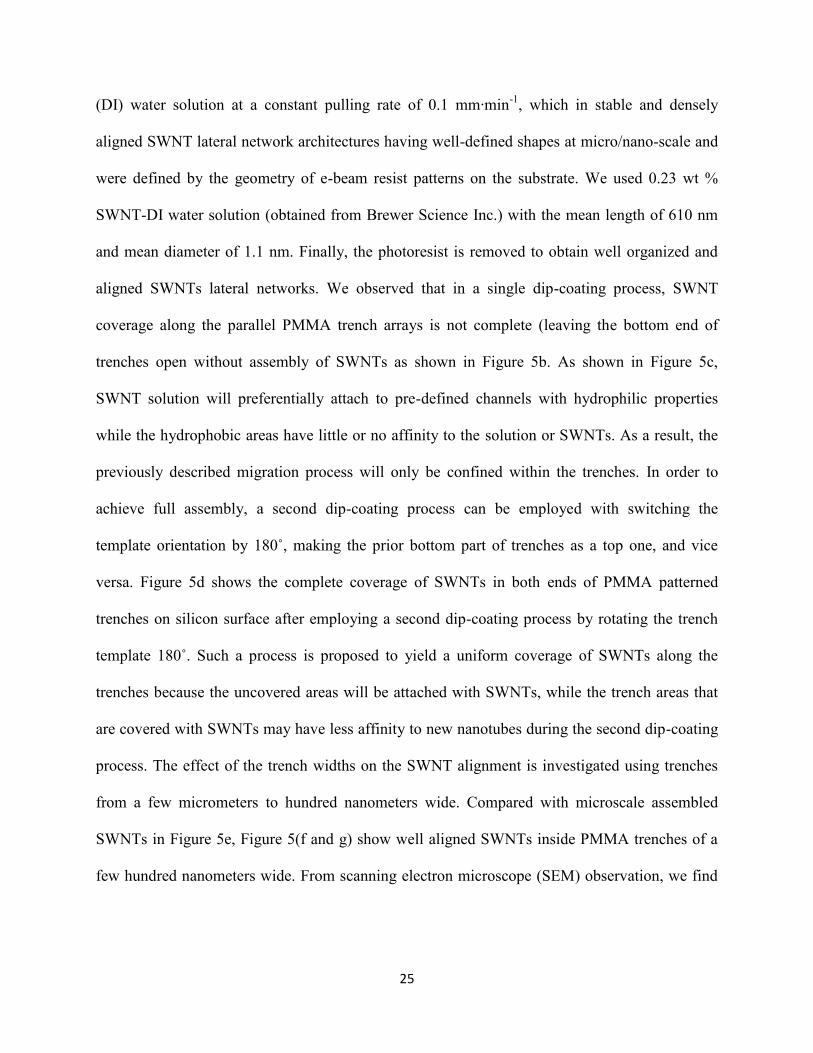
drastically. Figure 6 shows the results of the contact angle (Ө) measurement right after dropping
the SWNT-DI water solution on silicon substrates treated with plasma for times (5, 30, 60, and
90 sec). The lowest contact angle (the best hydrophilic behavior) of SWNT solution was
obtained with 5 sec plasma etched silicon substrate (0o) and the contact angle increased as the
plasma etching time increased. However, given enough time, the contact angle between all
silicon substrates and SWNT solution

27
Figure 6. Contact angle measurements. L. Jaber-Ansari, et al, JACS, 2008 [34].
Contact angle (Ө) measurement of Si substrate after 5, 30, 60, and 90 seconds of SF6/O2/Ar
plasma treatment. Contact angle change vs. time on the same substrates.
gradually changed to 0o. It also shows the change of the contact angle with the time after
depositing a droplet of the SWNT solution on these substrates. The result indicates that the 5 sec
plasma etched sample changes instantly to a completely hydrophilic surface while it takes more
time to produce hydrophilic groups for the longer plasma etched silicon substrates. SEM

28
Figure 7. Effect of plasma treatment on the surface morphology of Si. L. Jaber-Ansari, et al,
JACS, 2008 [34].
(a) AFM image of a 1 µm× 1 µm area of bare Si, (b1) AFM image of a 1 µm× 1 µm area of 5 s
plasma treated Si, (b2) SEM image of 5 s plasma treated Si, (c1) AFM image of a 1 µm× 1 µm
area of 90 s plasma treated Si and (c2) SEM image of 5 s plasma treated Si.
and atomic force microscopy (AFM) results for the 5 and 90 sec plasma treated Si surfaces are
shown in Figure 7. The 5 sec plasma etched sample (Figure 7b1) shows nano-structures on the
surface of silicon were 50 nm wide and 5 nm high, but the 90 s plasma etched sample (Figure
7c1) shows surface structures around 400 nm wide with a height variation of about 5 nm over
that area whereas in bare silicon the surface protuberances are only 100- 200 Å deep. These
surface structures can be seen as the grain shaped domains in the SEM images (Figure 7(b2 and
c2)). These results show an enormous increase in roughness after 5 sec plasma etching treatment

29
(Figure 7(b1 and b2)) and then a diminishing of the surface roughness with further etching of the
substrate (Figure 7(c1 and c2)). Although the AFM results show an increase in the physical
activity of the plasma treated substrates, such as enhanced roughness, the nature of the chemical
functional groups that are produced as the result of plasma treatment remains unclear. This
shows that a lot of dangling bonds exist on the surface of this substrate along with hydrophilic
OH- groups and hence the reason to hydrophilicity of such substrate. Therefore, the highly
increased surface area of the 5 sec plasma treated silicon along with the large number of
hydrophilic groups leads to the immediate change of surface to hydrophilic during contact angle
measurement (Figure 6); in 90 sec plasma treated sample, however, it takes longer for the surface
to become hydrophilic due to lower concentration of OH- groups and smaller surface area [34].
1.6 Topological Transitions in CNT Networks via Nanoscale Confinement
This section describes the topological transitions in organized SWNT networks modeled by Upmanyu
et al. [35]. Precise control over the electron transport in SWNT networks is challenging due to (i)
an often uncontrollable interplay between network coverage and its detailed topology and (ii) the
inherent electrical heterogeneity of the constituent SWNTs. In this reason, we explored the effect
of nanoscale confinement on carbon nanotube networks (CNNs) deposited on patterned channels
with varying width. While the resistivity strongly suggests a metallic-to-semiconductor transition
with decreasing width (see Figure 10d before Pt decoration), direct confirmation requires
detailed field characterization. To bypass the current experimental limitations and to capture the
effect of these network features in detail, we turn to systematic model computations of nanotube
assembly on experiment-scale channels. SWNTs coarse-grained as rigid rods are employed to
30
gain sufficient statistics on the interplay between topology and the nature of electrical
percolation within the network; the effect of channel width Wc is explored using 2D
computations, while multilayer, quasi-2D computations are used to study the effect of channel
thickness.
The random stick model that has been employed in earlier studies [36] is clearly inadequate in
capturing key phenomena such as SWNT bundling during self-assembly. In order to generate
realistic topologies, we further relax the network by allowing the coarse-grained SWNTs to
interact. The inter-CNT interactions, localized at the junctions, are obtained by integrating the
well-known Lennard-Jones (LJ) based description of the van der Waals between graphene
surface elements. As an example, for fully aligned SWNTs, the axially averaged inter-CNT
interaction energy per length U(R, r) is again a 6 - 12 LJ-type potential with constants that are
scaled by surface integrals which depend entirely on the ratio of the intertube distance to the
CNT radius R/r [37, 38]. Note that this intertube interaction is shortranged and negligible for R
√ ; that is, it is limited to first nearest neighbors. For partially aligned CNTs, the van der
Waals potential can again be integrated over the surfaces of the (pair) of CNTs. The resultant
effective inter-CNT interactions are angular as they now depend on the degree of misalignment
at the CNT - CNT junction φ, U U(R, r, φ). In the case of fully aligned bundles, this intertube
potential accurately describes equilibrium intertube spacing, cohesive energy per atom, and bulk
modulus. The interactions serve as inputs for classical dynamical simulations aimed at locally
relaxing the random network with respect to both translational and angular degrees of freedom of
the individual SWNTs. Sliding between the CNTs at the junctions is ignored. A time step of 1 µs
is employed, and the simulations are performed until the interaction energy associated with the
network stabilizes.

31
Figure 8a shows specific instances of the electrically heterogeneous network topologies
obtained in three simulations with varying widths, Wc = 1 µm, 500 nm, and 100 nm. In each case,
the SWNT network is confined, l/Wc > 1, which forces the topology to become increasingly
aligned with decreasing width. While the as-generated random topologies are geometrically
aligned along the channel, we find that the SWNT interactions always work toward increasing
the degree of alignment. This is not surprising as the orientation dependence of the interaction
potential favors a nematic-like phase consisting of fully aligned nanotubes [39]. For each relaxed
CNN with a prescribed network density, the electrical transport characteristics are extracted by
fixing the overall ratio of semiconducting-to-metallic SWNTs to the theoretical heterogeneous
density. To this end, each SWNT is randomly assigned a metallic or semiconducting character
and the overall percolation across the CNN is measured. The overall percolation can result in (i)
open circuit (OC), (ii) semiconducting, or (iii) metallic conductance across the network. Multiple
simulations (~ 100) are performed for each channel geometry and density to determine the form
of percolation.
Figure 8(b – d) shows the percolation probability through monolayered CNNs as a function of
the network density for the three widths shown in Figure 8a. All CNNs exhibit two transitions as
the network density is increased: OC-to-semiconducting at low densities, and a semiconducting-
to-metallic at high densities. Qualitatively similar transitions are also observed for unrelaxed
networks that are used as input in random stick models (shown as dotted lines), and comparisons
with percolation in relaxed structures indicate that the enhanced alignment driven by the SWNT
interactions shifts the transitions to higher network densities. The effect is dramatic at

32
Figure 8. Probabilities of CNNs and their contour plots. . Upmanyu, et al., ACS nano,2010 [35].
(a) CNNs observed in three different 2D simulations with varying channel widths, Wc = 1 µm,
500 nm, and 100 nm. In each case, 5 µm length of the 20 µm long channel is shown. For clarity,
detailed view of a 1 µm long segment of the W = 100 nm channel is also shown. Coloring
scheme is based on nature of electrical transport; blue and red indicate metallic and
semiconducting nanotubes, respectively. The relative number of metallic and semiconducting
nanotubes is fixed at the theoretical ratio, 1:3. (b - d) plots of the probability of the nature of
electrical percolation through the network as a function of network density, ρNT. The solid black,
red, and blue curves are probability of open circuit, semiconducting, and metallic conductance
across the network, respectively. The dotted lines correspond to simple stick percolation models
for randomly assembled networks. (e) Contour plot of the probability of semiconducting
behavior across the 2D network (shaded red) as a function of width (y-axis) and density (x-axis).
The length of the channel is fixed at L = 20 µm. (f) Same as in (e) but for multilayer, quasi-2D
simulations with varying channel thicknesses, t = 1 - 5 monolayers. The length and width of the
channels are fixed, L = 5 µm, W = 200 nm.
33
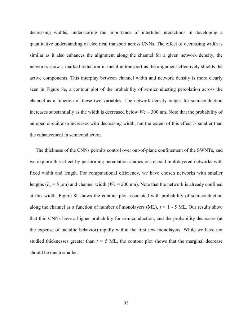
decreasing widths, underscoring the importance of intertube interactions in developing a
quantitative understanding of electrical transport across CNNs. The effect of decreasing width is
similar as it also enhances the alignment along the channel for a given network density, the
networks show a marked reduction in metallic transport as the alignment effectively shields the
active components. This interplay between channel width and network density is more clearly
seen in Figure 8e, a contour plot of the probability of semiconducting percolation across the
channel as a function of these two variables. The network density ranges for semiconduction
increases substantially as the width is decreased below Wc ~ 300 nm. Note that the probability of
an open circuit also increases with decreasing width, but the extent of this effect is smaller than
the enhancement in semiconduction.
The thickness of the CNNs permits control over out-of-plane confinement of the SWNTs, and
we explore this effect by performing percolation studies on relaxed multilayered networks with
fixed width and length. For computational efficiency, we have chosen networks with smaller
lengths (Lc = 5 µm) and channel width (Wc = 200 nm). Note that the network is already confined
at this width. Figure 8f shows the contour plot associated with probability of semiconduction
along the channel as a function of number of monolayers (ML), t = 1 - 5 ML. Our results show
that thin CNNs have a higher probability for semiconduction, and the probability decreases (at
the expense of metallic behavior) rapidly within the first few monolayers. While we have not
studied thicknesses greater than t = 5 ML, the contour plot shows that the marginal decrease
should be much smaller.
34
Chapter 2: Metallization of SWNT Network for Interconnect Applications
2.1 Introduction
As elements of integrated circuits downsize towards a few nanometers, existing interconnect
technology faces a tremendous bottleneck due to the electromigration failure of Cu lines [40, 41].
In addition, as the lateral dimension of interconnects approaches the mean free path of Cu (~40
nm at room temperature), the impact of grain boundary scattering, surface scattering, and the
presence of a high-resistivity material as a diffusive barrier layer causes a rapid increase in their
overall resistivity. In this context, CNTs have been envisioned as a possible replacement for Cu
electrical interconnects for future gigascale integration considering their immense individual
failure current densities (> 109 A·cm
-2) [42, 43].
Especially at the nanoscale, highly aligned
parallel nanotube architectures comprising of all-metallic SWNTs are expected to outperform Cu
in terms of failure current density, power dissipation, and on-chip signal transfer delays [44, 45].
However, to fabricate such highly aligned SWNT-based interconnects in an integrated device, a
complementary metal-oxide-semiconductor (CMOS)-friendly scalable manufacturing process
that can controllably place aligned SWNTs in desired locations, orientations, and dimensions is
extremely crucial. In addition, since naturally grown SWNTs comprise of a mixture of metallic
and semiconducting nanotubes, there is an imminent need to develop a process that will convert
semiconducting nanotubes into metallic ones within such architectures. Therefore, a single-step,
simple, and CMOS compatible method that can simultaneously convert semiconducting SWNTs
into metallic ones, and also possibly increase the conductance of existing metallic SWNTs, is

35
highly desirable. Addressing these technological challenges is essential before carbon nanotubes
can be realistically implemented as future interconnects.
Recently, we have demonstrated a novel template-based fluidic assembly process for
fabricating highly organized SWNT lateral network architectures at wafer scales [33, 34]. We
have also shown that the conductance of individual MWNTs can be improved significantly by
decorating its surface with Pt nanoclusters [46]. Field theoretical analysis confirm that this is
caused by the increase in the number of conductance channels of the nanotubes. Ab-initio density
functional theory (DFT) calculations indicate that charge transfer from decorated Pt nanoclusters
on nanotubes can increase the number of bands near the Fermi level of the nanotubes, and
increase their density of states (DoS). DFT calculations also show that Pt-nanoclusters can
convert semiconducting SWNTs into metallic ones, and improve the conductance of metallic
nanotubes as well.
In this chapter, we combine these ideas to develop highly organized aligned arrays/channels
of Pt-decorated SWNT interconnect test structures, with vastly improved performance over
pristine SWNT architectures. In general, we find that the nanotube alignment improves
noticeably with decreasing lateral channel widths, with the best alignment obtained for widths
close to 200 nm. Significantly robust against the lithographic and electrodeposition steps, these
interconnect test structures were capable of withstanding current densities up to ~107 A∙cm
-2.
Upon Pt decoration, the average electrical resistivity of these SWNT interconnect test structures
decreased by 45%, with a 52% drop for the narrowest channels. In more than 25% of the tested
structures, the resistance of the Pt-decorated structures fell to 1/3rd
of its pristine value, indicating
that most of the semiconducting nanotubes between the Ti/Au-contacted SWNT arrays have
converted to metallic ones. In a few cases, this value fell below 1/3rd
, indicating that the

36
conductance of the metallic nanotubes have gone up as well. These completely CMOS-
compatible and scalable process steps together reflect a huge step towards integration of carbon
nanotubes into existing interconnect technologies.
2.2 Fabrication of Highly Aligned SWNT Lateral Architectures
Figure 9 shows representative scanning electron microscopy (SEM) images of our aligned
SWNT lateral architectures fabricated on SiO2/Si substrates using our template guided fluidic
assembly process. Figure 9a schematically explains the basic steps of building organized SWNT
lateral architectures described in chapter 1.4. Figure 9b is an SEM image of a typical SWNT
lateral structure attached on top with two contact pads of Ti/Au, fabricated using a standard EBL
process. Figures 9c – 9e are higher magnification SEM images showing the relative alignments
of lateral SWNTs along the channels with approximate widths of 1000 nm, 500 nm, and 200 nm
respectively. An important outcome of our SWNT assembly technique is that the degree of
alignment of SWNT structures tends to increase with lower channel widths.
2.3 Detailed Study of the Alignment of SWNT Architectures
Polarized Raman spectroscopy has been used in the past to study the symmetry of the
vibrational modes of carbon nanotubes [47]. Using this technique, past workers have reported
study of SWNT alignment in fibers [48]. In particular, the tangential modes give rise to a number
of Raman active peaks at positions between 1550 cm-1
– 1610 cm-1
. By changing the

37
Figure 9. Schematic and SEM images showing super-aligned SWNT interconnect structures.
a) Schematic showing template-based fluidic assembly of high density and highly aligned SWNT
architectures. b) SEM image of typical SWNT lateral structures with two-probe contact pads.
Scale bar = 2 μm. c) – e) High magnification SEM images showing the degree of alignement of
the SWNTs within channel widths of ~1000 nm, ~500 nm, and ~200 nm respectively. Scale bars
= 200 nm.
polarization of the Raman Laser with respect to the alignment direction of our arrays, and noting
the relative intensities of the largest tangential peak (with respect to the intensity of the same
peak in an unpolarized Raman spectrum), it is possible to quantify the degree of alignment of our
SWNT arrays.
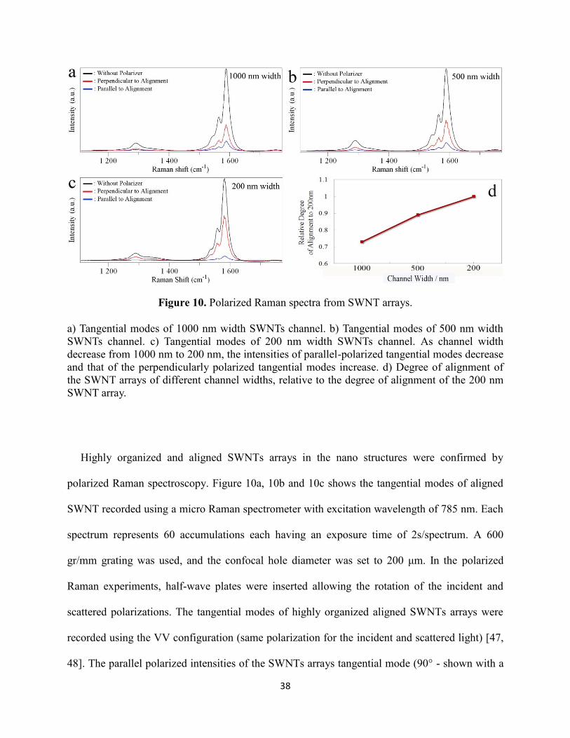
38
Figure 10. Polarized Raman spectra from SWNT arrays.
a) Tangential modes of 1000 nm width SWNTs channel. b) Tangential modes of 500 nm width
SWNTs channel. c) Tangential modes of 200 nm width SWNTs channel. As channel width
decrease from 1000 nm to 200 nm, the intensities of parallel-polarized tangential modes decrease
and that of the perpendicularly polarized tangential modes increase. d) Degree of alignment of
the SWNT arrays of different channel widths, relative to the degree of alignment of the 200 nm
SWNT array.
Highly organized and aligned SWNTs arrays in the nano structures were confirmed by
polarized Raman spectroscopy. Figure 10a, 10b and 10c shows the tangential modes of aligned
SWNT recorded using a micro Raman spectrometer with excitation wavelength of 785 nm. Each
spectrum represents 60 accumulations each having an exposure time of 2s/spectrum. A 600
gr/mm grating was used, and the confocal hole diameter was set to 200 μm. In the polarized
Raman experiments, half-wave plates were inserted allowing the rotation of the incident and
scattered polarizations. The tangential modes of highly organized aligned SWNTs arrays were
recorded using the VV configuration (same polarization for the incident and scattered light) [47,
48]. The parallel polarized intensities of the SWNTs arrays tangential mode (90° - shown with a
39
blue line) decreased as the SWNTs channel width decreases from 1000 nm to 200 nm (10a to
10c). On the other hand, it is clearly seen that, as the size of SWNTs array decreases from
1000nm to 200 nm (10a to 10c), the perpendicular polarized intensities of tangential mode (0°,
red line) increase. Figure 10d shows the relative degree of alignment of aligned SWNTs arrays
(1000 nm, 500 nm and 200 nm), the degree of alignment calculated by ratio of the relative
polarized Raman intensities of SWNT arrays (at 1583 cm-1
) with respect to that of the 200 nm
SWNTs array since G band intensity is closely related with the population of graphitic structure.
We find that the degree of alignment increase as the array width decrease from 1000 nm to 200
nm. We believe that the increasing alignment occur during the dip-coating process due to the
increasing confinement of the PMMA trench geometry with decreasing channel widths.
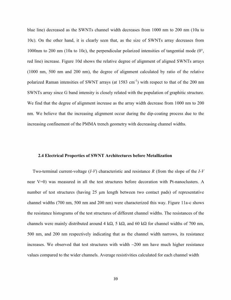
2.4 Electrical Properties of SWNT Architectures before Metallization
Two-terminal current-voltage (I-V) characteristic and resistance R (from the slope of the I-V
near V=0) was measured in all the test structures before decoration with Pt-nanoclusters. A
number of test structures (having 25 μm length between two contact pads) of representative
channel widths (700 nm, 500 nm and 200 nm) were characterized this way. Figure 11a-c shows
the resistance histograms of the test structures of different channel widths. The resistances of the
channels were mainly distributed around 4 kΩ, 5 kΩ, and 60 kΩ for channel widths of 700 nm,
500 nm, and 200 nm respectively indicating that as the channel width narrows, its resistance
increases. We observed that test structures with width ~200 nm have much higher resistance
values compared to the wider channels. Average resistivities calculated for each channel width

40
Figure 11. Electrical characteristization of aligned SWNT interconnect structures.
a) – c) Resistance histograms of pristine devices. The values were distributed mainly around 4
kΩ, 5 kΩ, and 60 kΩ for channel widths of 700 nm, 500 nm, and 200 nm respectively. d)
Current-voltage (I-V) curves between different contact pads A, B, and C separated by a distance
of 10 μm between them (as shown in the inset schematic) for calculation of contact resistances
(see text).
(see figure 14d) show an increasing trend when the channel width is decreased indicating
increasing semiconducting behavior as the channel width narrows down. Similar observations
have been experimentally reported for random SWNT mats with decreasing height [49]. Since
we do not yet have a clear understanding of the self alignment mechanism of SWNTs during the
assembly process, especially the degree of alignment with different channel widths, at this stage
we cannot explain this related electronic property change. However, based on previous studies of
percolation theory of SWNT networks [50, 51], we feel that the alignment of SWNTs in
41
narrower channels statistically reduces the formation of metallic conduction paths between the
two contacts, resulting in a dominant semiconducting property of the arrays.
To estimate the contact resistance for a given test structure, three contact pads (A, B, and C)
separated by a distance of 10 μm were fabricated for each representative channel width. I-V
measurements were performed between pairs of contact pads A–B, B–C, and A–C as shown in
Figure 11d. The inset shows a schematic of these three contact pads on the test structures. The
measured resistance (from the slope of the I-V curves) between the contact pads A and B can be
written as RAB = RCA + RDAB + RCB, where RCA (or RCB) = contact resistance at pad A (or B) and
RDAB = device resistance between pads A and B. In this way, the contact resistance at pad B, RCB
can be written in terms of RAB, RBC and RCA as:
(2.1)
From three different test structures for each channel width, we found that the contact resistance
was within 20% of the total resistances of the test-structure. These values did not change
appreciably after the Pt-decoration experiments described later.
2.5 ab-initio Density Functional Theory Calculations
Having characterized the pristine interconnect test structures, we now turn towards
maximizing their electrical properties for interconnect applications. As-received SWNTs are a
mixture containing approximately 2/3rd
semiconducting and 1/3rd
metallic carbon nanotubes. In
aligned architectures such as ours, due to the high resistance of the semiconducting nanotubes

42
(almost 2-3 orders of magnitude larger than that of metallic nanotubes) [52], only 1/3rd
of the
nanotubes actively conduct current, and the rest remain dormant, vastly degrading the potential
performance of the interconnect structure. Hence, it is essential to change the electrical property
of semiconducting nanotubes into metallic ones for nanoscale interconnect applications.
Moreover, we find that our narrower lateral SWNT architectures tend to have higher resistivity,
presumably due to decreased number of metallic conduction paths within the nanotube arrays.
Our past work has shown that Pt-decoration of carbon nanotubes can be an effective method for
increasing the number of conduction channels near the Fermi level [46], which increases the
conductance of multi-wall carbon nanotubes. Question arises if similar effects can be used to
improve conductance of SWNTs as well. To elucidate the possible underlying effects of Pt-
nanocluster decoration on the electronic band structure of metallic and semiconducting SWNTs,
we first present ab-initio Density functional theory (DFT) calculations on these systems. The
calculations are based on a super cell approach with periodic boundary conditions, where Pt-
clusters lie at the center of each supercell. Detailed calculations were performed for two
semiconducting SWNTs (with chiralities [8,0] and [10,0]) and one metallic ([9,0]) SWNT, for
increasing number of Pt atoms (n = 0-13) per cluster. Our calculations show that the introduction
of Pt-atoms gives rise to new electronic bands near the Fermi level of all the SWNTs that
directly impacts the band gap, which defines the semiconducting or metallic nature of the
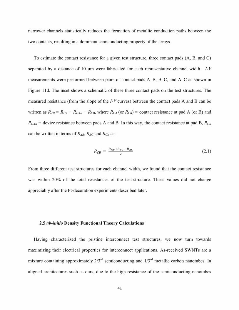
nanotubes. Figure 12a shows the variation of band gap EG in the three SWNTs for different
number of Pt-atoms, n, per cluster. We see that with increasing number of Pt atoms per cluster,
the band gaps of the semiconducting nanotubes [8,0] and [10,0] rapidly approach EG 0 by
n=3, and then remain close to zero for n>3. For the metallic nanotube [9,0], the gap remains very
close to zero for almost all values of n. Further, the proximity of these additional bands to the
43
Figure 12. Calculations of the effect of Pt-decoration on electronic properties of SWNTs.
a) Band-gap closing in semiconducting [8,0] and [10,0] SWNTs due to Pt-nanocluster decoration.
The gaps close within 3-Pt coverage and then remain close to zero. The metallic [9,0] nanotube
remains metallic after 3-Pt coverage. b) Effect of Pt-decoration on the zero-bias Landauer
conductance at T=300K in a semi-log plot. The conductance of the semiconducting nanotubes
[8,0] and [10,0] increases by several orders of magnitude and approach G=4e2/h within 3-pt
decoration, and fluctuate close to this value. The metallic [9,0] nanotube continues to remain
metallic without any significant drop in conductance, and in some cases the conductance in both
metallic and semiconducting nanotubes, G exceeds 4e2/h. The insets represent the optimized
structure of representative cluster sizes. The purple atoms are the last ones to be added.
44
Fermi level enhances their contribution to the total conductance compared to the pristine SWNTs.
Figure 12b shows a semi-log plot of the zero-bias Landauer conductance [53, 54] as a function of
number of Pt atoms per cluster for all three SWNTs, calculated at T=300K. It is seen that the
semiconducting nanotubes undergoes 4-5 orders of magnitude increase in conductance within as
low as n=3, approaching the value G=4e2/h. For n>0, G remains orders of magnitude more
conducting compared to the pristine systems, and significantly close to 4e2/h, which makes them
metallic for all practical purposes. The metallic (9,0) nanotube continues to remain metallic. In
all cases, the conductance of nanotube exceeded 4e2/h for certain values of n. This indicates that
uniform decoration of small (few nanometers) clusters of Pt can potentially convert
semiconducting SWNTs into metallic ones, and further enhance the conductance of metallic
nanotubes [55].
2.6 Pt Decoration of SWNT Architectures
Hence, we have adopted this procedure of Pt-nanocluster decoration to improve the overall
conductivity of our SWNT interconnect arrays. Pt nanoclusters were electrochemically decorated
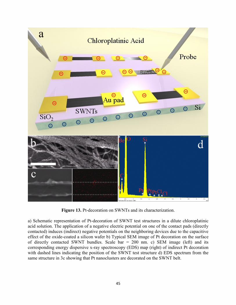
on the SWNT arrays without disturbing their aligned architecture. Figure 13a is a schematic of
the Pt decoration process on SWNTs. To decorate Pt nanoclusters on the surface of SWNTs, we
immersed the assembled SWNT test structures in a 5 mM chloroplatinic acid solution. A
negative potential (-Ve) of 50 mV was applied on a contact pad for 2 seconds using a Keithley
2400 sourcemeter, and the other probe was immersed in the same solution without touching any
contact pads. When a negative potential is applied to the contact pad of the test structures, Pt ions
having positive charges are nucleated selectively on the surface of the contact
45
Figure 13. Pt-decoration on SWNTs and its characterization.
a) Schematic representation of Pt-decoration of SWNT test structures in a dilute chloroplatinic
acid solution. The application of a negative electric potential on one of the contact pads (directly
contacted) induces (indirect) negative potentials on the neighboring devices due to the capacitive
effect of the oxide-coated a silicon wafer b) Typical SEM image of Pt decoration on the surface
of directly contacted SWNT bundles. Scale bar = 200 nm. c) SEM image (left) and its
corresponding energy dispersive x-ray spectroscopy (EDS) map (right) of indirect Pt decoration
with dashed lines indicating the position of the SWNT test structure d) EDS spectrum from the
same structure in 3c showing that Pt nanoclusters are decorated on the SWNT belt.

46
pads and the SWNT architectures. At the same time, induced negative potential is created on the
neighboring test structures by a capacitive effect of the underlying highly doped Si substrate and
its SiO2 insulating layer. This resulted in decoration of smaller Pt nanoclusters (< 5 nm) on the
surface of the other assembled SWNT arrays as well. We found that this “indirect” deposition
was more effective as it gave clusters of extremely small size, and there were no damages to the
arrays due to accidental static discharge when the probes are contacted to the pads. Figure 13b is
an SEM image of SWNT arrays on which Pt nanoclusters, decorated directly, are clearly visible.
Figure 13c shows an SEM image and energy dispersive x-ray spectroscopy (EDS) maps of an
SWNT array indirectly decorated with Pt nanoclusters. In this case, the Pt-clusters were almost
indistinguishable in the SEM images, but the EDS map for Pt shows very small amounts of Pt
decoration, as confirmed by the EDS spectrum in figure 13d. The EDS map along with the
spectral analysis is consistent with the fact that extremely small (~ a few nanometers) Pt
nanoclusters are uniformly decorated over the surface of aligned SWNT network structures
without forming a continuous Pt film. The small amount of Pt-nanoclusters in the surrounding
region of the SWNT array was decorations on the SiO2 surface and did not contribute to the
conducting mechanism in any way. This was confirmed by physically breaking some of the test
structures after which no current was detected between the contact pads when a voltage was
applied.
2.7 Electrical Properties of Highly Aligned SWNT Structures after Pt Decoration
Figures 14a-c shows change in resistance before and after Pt-decoration for samples having
widths approximately = 700 nm, 500 nm, and 200 nm (with five test structures for each width),
47
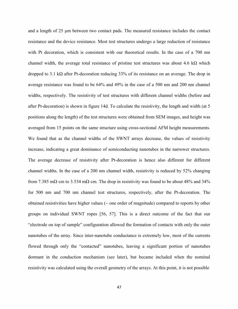
and a length of 25 μm between two contact pads. The measured resistance includes the contact
resistance and the device resistance. Most test structures undergo a large reduction of resistance
with Pt decoration, which is consistent with our theoretical results. In the case of a 700 nm
channel width, the average total resistance of pristine test structures was about 4.6 kΩ which
dropped to 3.1 kΩ after Pt-decoration reducing 33% of its resistance on an average. The drop in
average resistance was found to be 64% and 49% in the case of a 500 nm and 200 nm channel
widths, respectively. The resistivity of test structures with different channel widths (before and
after Pt-decoration) is shown in figure 14d. To calculate the resistivity, the length and width (at 5
positions along the length) of the test structures were obtained from SEM images, and height was
averaged from 15 points on the same structure using cross-sectional AFM height measurements.
We found that as the channel widths of the SWNT arrays decrease, the values of resistivity
increase, indicating a great dominance of semiconducting nanotubes in the narrower structures.
The average decrease of resistivity after Pt-decoration is hence also different for different
channel widths. In the case of a 200 nm channel width, resistivity is reduced by 52% changing
from 7.385 mΩ·cm to 3.534 mΩ·cm. The drop in resistivity was found to be about 48% and 34%
for 500 nm and 700 nm channel test structures, respectively, after the Pt-decoration. The
obtained resistivities have higher values (~ one order of magnitude) compared to reports by other
groups on individual SWNT ropes [56, 57]. This is a direct outcome of the fact that our
“electrode on top of sample” configuration allowed the formation of contacts with only the outer
nanotubes of the array. Since inter-nanotube conductance is extremely low, most of the currents
flowed through only the “contacted” nanotubes, leaving a significant portion of nanotubes
dormant in the conduction mechanism (see later), but became included when the nominal
resistivity was calculated using the overall geometry of the arrays. At this point, it is not possible

48
Figure 14. Electrical properties of SWNT structures before and after Pt decoration.
a) – c) Resistance of pristine and Pt-decorated devices with 700 nm, 500 nm, and 200 nm
channel widths. Most Pt-decorated structures exhibited dramatically reduced resistance
compared to their pristine states. d) Resistivity of structures with different channel widths before
and after Pt decoration. e) Failure current density with a guide curve for structures having
various channel widths, showing that narrower devices have better current-handling capability.
to determine the exact number of “uncontacted” nanotubes. However, our future research will
attempt to overcome this problem by fabricating arrays of extremely small heights (less than a
few nanometers).
The larger percentage drop in resistivity for the narrower channels is consistent with the fact
that before Pt-decoration, the overall fraction of semiconducting nanotubes between the two
contacts was larger for narrower channels, which, when converted to metallic nanotubes, causes
a higher percentage change. If every contacted semiconducting nanotube were to be completely

49
converted to metallic one in all the test structures, the final resistivity would be independent of
channel size. From figure 14d, (where average values for 5 test structures have been plotted for
each channel width) we find that complete “metallization” of all nanotubes in all test structures
were not achieved due to variations in experimental conditions, although the slower dependence
of resistivity on channel-width, after Pt-decoration, compared to that of the pristine structures is a
very encouraging result. We will discuss this metallization issue in greater detail later on.
Another important criterion for interconnect applications is the failure current density.
Individual MWNT can withstand current densities of ~ 109 A·cm
-2 at 300°C for a short time [42].
Also, MWNT via structures were shown to operate at a current density of 2×10⁶ A·cm
-2,
comparable to Cu vias [58]. Individual SWNTs can withstand a current density > 109 A·cm
-2
[59]. However, it appears that such high current densities in highly organized and aligned lateral
SWNT structures have not been reported so far. Failure current density was measured in our
structures by increasing an applied voltage in steps of 3 V in a vacuum chamber. Figure 14e
shows failure current density (the dashed line is a guide to the eye) for test structures with
different channel widths. The averaged value of failure current density was 7.34x10⁶ A·cm
-2,
while the maximum failure current density was measured up to 9.62x10⁶ A·cm
-2 obtained for the
narrower channels. Although these values are lower than that of individual metallic CNTs, we
note that even for these calculations, we have assumed that all the nanotubes participate in the
conduction of charges, whereas in reality only a part that is electrically contacted conducts the
charge carriers, hence lowering the calculated current density. In any case, the values are larger
than that of MWNT via bundles, and increases for lower channel widths, easily comparable or
better than that of Cu at these size-scales.

50
The apparent lack of any measurable accumulation of damage over time suggests that the
strong, covalently bonded carbon atoms in individually wired CNTs may not be subject to
electromigration, as further supported by the observed electromigration resistance of CNT– Cu
composite interconnects [60, 61]. However, all of these studies were based on single CNT
failures without any repeated experiments to confirm the results and gather statistics. Moreover,
the long-term performance and reliability of CNT-based devices have been largely neglected,
despite their likely exposure to significant current densities and high temperatures that may
directly induce thermal failure [62], cause thermal– mechanical fatigue or stimulate de-adhesion
and significant interdiffusion at critical interfaces between CNTs, metals, dielectrics and
polymers [63, 64]. To test reliability of SWNT networks, super-aligned networks of SWNTs,
such as the one shown in Figure 9e, were fabricated for this reliability test. All measurements
were obtained by the use of pseudo four-terminal sensing in air at room temperature with a
commercial power supply, where both the applied voltage source and current sensing tungsten
probes were placed on the same Ti/Au electrode pairs. Thus, the measurement probe resistances
were removed from the resistance measurement of the total system, but the contact resistance
between the SWNTs and Ti/Au electrode was included. In this work, we report only total line
resistance, which includes the resistances of the CNT–electrode interface, the individual SWNTs
and the SWNT–SWNT junction resistances. Each networked SWNT line was subjected to a
constant DC input voltage Vinput, which was varied from line to line, while the current (Imeasure)
was collected as a function of time. The input voltage was always ramped from 0 to Vinput over
the course of several minutes. The magnitude of Vinput was chosen differently for each line to
explore the effect of the electrical stress magnitude. If the chosen values of Vinput were too small
(typically <4 V), the lines would last several days with no signs of damage. The SWNT array
51
lines were placed on a heat-controlled chuck, and the resistance was found to decrease
nonlinearly with an increase in temperature, as is typical of other SWNT networks [65, 66]. The
current densities in the networked CNT lines were found to be between 0.93 and 9.7MA·cm-2
, as
calculated by dividing the maximum Imeasure in each line by the cross-sectional area of a ‘typical’
line, assuming full packing density [67]. Actual current densities in individual SWNTs were
probably higher, because it was likely that some of the SWNTs in the cross section did not
conduct equally or at all, and the SWNT packing density must be <1.
2.8 Calculation of Resistance before and after Pt Decoration
If, as our DFT results indicate, the Pt-decoration indeed results in the enhanced metallic
behavior of individual nanotubes, it is important to investigate the degree of metallization that
the semiconducting nanotubes in the test structures undergo. As discussed earlier, the electrode-
on-top configuration does not contact all the nanotubes electrically. Hence, from the resistivity
values itself, it is not possible to comment on how many semiconducting nanotubes were
converted to metallic ones. However, since the same number of nanotubes remain in contact with
the leads before and after the Pt-decoration, we can use the known ratio of semiconducting to
metallic nanotubes (2:1) for naturally grown SWNTs, to predict the overall change in resistance
if all semiconducting tubes were converted to metallic ones. We assume that this ratio is
extendable to the two kinds of nanotube paths (metallic or semiconducting paths) between the
two contacts of our aligned array.

52
Let us assume that, in any test structure, the number of nanotubes is X and the number of
nanotubes electrically contacted is N, where N < X (e.g. N could be equal to 30% of X). Out of
these N nanotubes, N/3 are metallic and 2N/3 are semiconducting ones. In the simplest case, if
we assume that the nanotubes are parallel resistors in the device, the total resistance of the
pristine array of nanotubes is,
∑
∑
(2.2)
where Rm is the resistance for a metallic SWNT and Rsc is resistance for a semiconducting
SWNT.
To simplify calculations, let us assume that all metallic SWNTs have resistance of Rm and
semiconducting SWNTs have resistance of Rsc. Then, equation (2) can be written as
∑
∑
⁄
⁄
. (2.3)
Typically, Rsc ≫ Rm by about two to three orders of magnitude. In this case, the term
∑
⁄
compared to the term, ∑
⁄
. Therefore, resistance of device before Pt
decoration can be written as
(2.4)
After Pt decoration, if all semiconducting SWNTs get converted to metallic ones, then their
converted resistance is same as that of the metallic SWNTs (i.e. Rm). Therefore, the total
resistance after Pt-decoration would be given by,

53
Figure 15. Comparison between predicted and experimentally measured resistance ratio of Pt-
decorated and pristine test structures.
∑
∑
⁄
⁄
⁄
⁄
. (2.5)
Hence, the resistance of device after Pt decoration can be written as:
. (2.6)
Hence, the predicted ratio of resistance between the decorated and pristine test structures,
⁄
⁄
, (2.7)

54
which is independent of how many SWNTs are electrically contacted.
Figure 15 shows the comparison between the predicted value and experimental results for the
ratio of resistance before and after Pt decoration for all test structures of different channel widths.
The test structures have been plotted in increasing order of the ratio values for clarity. We find
that more than 25% devices attained the predicted ratio of 0.33 (indicating conversion to “all-
metallic” test-structures after Pt-decoration). In case of the other test structures, the process of Pt
decoration may have been incomplete due to variabilities associated with our electrodeposition
experiments in terms of time, concentration of electrolytes, electric fields, access to all nanotubes
etc., and these issues will be addressed in future. In some cases, the ratio was below 0.33,
indicating that some of the metallic nanotubes may have undergone conductance enhancement as
well, as predicted by density functional theory calculations. Our future research will attempt to
fabricate test structures of very low heights such that all the nanotubes can be electrically
contacted. This will remove many of the discussed ambiguities that have evolved during this
work.
2.9 Conclusions
In conclusion, using a template-guided fluidic assembly process, we have fabricated highly
organized, scalable and aligned SWNT array interconnect test structures. The narrowest lateral
widths of test structures presented here (~200 nm) are limited by our current lithographic
facilities and in principle can be reduced further down to lower sizes. The structures become
increasingly aligned with decreasing channel width. We have also demonstrated a Pt nanoclusters

55
decoration technique to enhance the overall conductive nature of these structures. Due to our top-
contacted geometry that did not electrically contact all the nanotubes, accurate estimates of
resistivity of the nanotube array was not possible. However, the Pt-decoration leads to significant
reduction of the nominal channel resistivity, with evidence of complete conversion of the
semiconducting nanotubes into metallic ones in some cases, in agreement with our calculations
of band gap and Landauer conductances. These interconnect test structures are able to handle
high current densities, approaching nominal values of ~107 A∙cm
-2 (comparable to or better than
that of Cu). The processes involved in the fabrication and performance enhancement via Pt-
decoration are simple to implement, are CMOS compatible, and easily scalable to wafer levels.
The fabrication and performance enhancement of these interconnect test structures demonstrate a
big step towards integration of carbon nanotubes into microelectronic platforms for future
gigascale interconnects.

56
Chapter 3: Reducing Interfacial Contact Resistance of Organized SWNT
Interconnect Structures
3.1 Introduction
The continuous downsizing of active elements such as memories, switches, and transistors in
a bid to improve the overall microprocessor performance is beginning to pose severe constraints
on the reliability of interconnects, which transfer signal and power to and between these active
elements†. In particular, issues related to electromigration failure and increasing resistivity due to
surface and grain boundary scattering in conventional Cu interconnects of widths below its mean
free path (~40 nm) lead to critical concerns regarding their increased power dissipation, signal
transfer delays, and ultimate reliability. This has generated a strong motivation for seeking
alternative materials for future interconnect technologies. In this context, densely aligned,
horizontally organized SWNT networks are promising candidates for replacing Cu-based
interconnects in future microprocessors†.
Over the years, CNTs have gained prominence for their enormous potentials for nanoscale
electronic [68, 69] and electromechanical devices [70-72] due to their one-dimensional nano-
structure, high electron mobility [73], huge failure current density [42], (orders of magnitude
higher than that of Cu), and outstanding mechanical stability. In our previous works [74-76] we
had demonstrated a unique, CMOS-compatible method for assembling SWNTs in the form of
horizontally organized networks with controllable geometries with widths down to 200 nm.
These SWNT networks could handle nominal current densities in excess of 107 A/cm
2. We also
demonstrated a method for improving their conductance via a Pt-nanocluster decoration method
† International Technology Roadmap For Semiconductors, 2009 Edition: Interconnects.
http://www.itrs.net/Links/2009ITRS/2009Chapters_2009Tables/2009_Interconnect.pdf

57
[75]. These architectures are attractive for building horizontally organized SWNT interconnects.
However, several issues need to be addressed before these can be realistically integrated into
existing interconnect device platforms. Among these, one issue of key importance is that of
contact resistance at SWNT – metal interfaces.
Due to its unique one-dimensional electronic structure, individual CNTs will always have a
minimum quantum contact resistance at the metal-nanotube interface. This quantum contact
resistance has been theoretically predicted and experimentally demonstrated [77] to be = h/4e2
6.5 kΩ due to their four available conduction channels, where h is Planck’s constant and e is the
charge of electron. In horizontally organized SWNTs, where thousands of nanotubes are
expected to conduct in parallel, the effect of quantum contact resistance becomes negligible.
However, in addition to this, interfacial contact resistance, which results from the formation of
imperfect bonds between metals and SWNTs, or due to the presence of impurities, can
additionally cause high contact resistance. For example, Yao et al. [78] reported a metallic
SWNT with two-terminal resistances as high as 110 kΩ at room temperature. In fact, developing
metal-SWNT interfaces with low interfacial contact resistance is the one of key challenges in
fabricating interconnect structures using CNTs†. Researchers have attempted various methods to
reduce the contact resistance between CNTs and metals [79-81]. Bachtold et al. [82] showed the
decrease of contact resistance of MWNTs deposited on Au contact pads by selectively exposing
MWNTs to an electron beam. Dong et al. [83] studied local Joule heating processes that could
reduce the contact resistance between individual CNTs and metallic electrical contacts. However,
these methods are not easy to implement as a wafer-scale protocol for interfacial contact-
resistance-free SWNT networks, which is required in order to implement them as future SWNT
interconnects. In this chapter, we report the investigations of a number of extra cleaning steps
† International Technology Roadmap For Semiconductors, 2009 Edition: Interconnects.
http://www.itrs.net/Links/2009ITRS/2009Chapters_2009Tables/2009_Interconnect.pdf

58
during the SWNT-metal interconnect fabrication process that renders lower contact resistances
between SWNTs and metal contacts of Ti/Au. Under optimal conditions the average interfacial
resistance at a metal-SWNT was found to be 15 Ω, which is less than 1 % of the SWNT network
resistance. The significant decrease of contact resistance in our SWNT networks using wafer-
scale implementable processes represent a big step towards utilizing SWNTs for future nanoscale
electrical interconnects.
3.2 Fabrication of Organized SWNT Interconnect Structures
Highly organized SWNT networks were fabricated using a template-guided fluidic assembly
method reported previously [75]. Briefly, this method uses lithographically fabricated linear poly
methyl methacrylate (PMMA) patterns on a plasma-treated SiO2/Si substrate as templates (see
Figure 5a) that provide channels of well-defined widths described in chapter 1.4. Figure 16
shows scanning electron microscope (SEM) images of aligned SWNT networks with different
widths. It is found that the alignment improves significantly with decrease in channel width [75,
80] – a fact that makes them extremely favorable for low dimensional interconnects (sub-100
nm). Figure 16d shows an interconnect test structure device with multiple contacts fabricated
using an EBL. The dimension of interfacial area between metallic electrodes and a bundle of
SWNTs is 1µm width and 2µm length with metal electrodes on the top of SWNT line structures.
3.3 Measurement of Contact Resistance
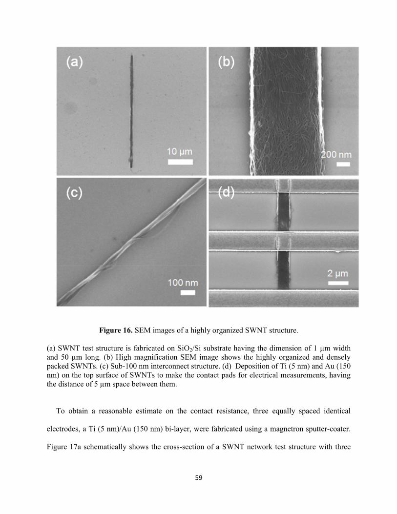
59
Figure 16. SEM images of a highly organized SWNT structure.
(a) SWNT test structure is fabricated on SiO2/Si substrate having the dimension of 1 µm width
and 50 µm long. (b) High magnification SEM image shows the highly organized and densely
packed SWNTs. (c) Sub-100 nm interconnect structure. (d) Deposition of Ti (5 nm) and Au (150
nm) on the top surface of SWNTs to make the contact pads for electrical measurements, having
the distance of 5 µm space between them.
To obtain a reasonable estimate on the contact resistance, three equally spaced identical
electrodes, a Ti (5 nm)/Au (150 nm) bi-layer, were fabricated using a magnetron sputter-coater.
Figure 17a schematically shows the cross-section of a SWNT network test structure with three
60
electrical contact pads (A, B, and C) for measuring contact resistance as well as overall
resistance of SWNT network. Typical current-voltage (I-V) dependences for the contact
resistance measurement are plotted in Figure 17b, showing a linear dependence of current with
voltage. The estimation of interfacial contact resistance assumes that the two-terminal resistance
(inverse slope, dV/dI) between any two electrodes (e.g. RAB between A and B) is the sum of the
device resistance (i.e. quantum contact resistance + resistance due to scattering within the
nanotubes) of the SWNT networks and the interfacial contact resistance at each contact. From
the two-terminal I-V characteristics, the resistance R was measured in all test structures which
have a width of 1 µm. The three contact pads were separated by the distance of 5 µm from each
other. I-V measurements were conducted between the pairs of A – C, A – B, and B – C. The
contact resistance at contact pad B, RcB can be written in term of RAB, RBC, and RAC as
(3.1)
where RAB = RcA + RdAB + R
cB, RBC = R
cB + RdBC + R
cC, and RAC = R
cA + RdAC + R
cC [75]. The
resistance RdAB is defined as a device resistance between a contact pad A and B. Since the
electrodes were identically fabricated, the contact resistance at the center lead B can be assumed
to be similar to those of A and C, apart from that arising from a small amount of inhomogeneity
of the SWNT alignment at each of these leads. An alternate method for obtaining contact
resistance that involves separately measuring the resistances by 2-probe and 4-probe methods
and comparing the two, introduces a similar amount of error compared to our proposed method.
Hence we chose to use our presented method for estimation of contact resistances, and we
present our data in the form of percentage changes. In all devices, this fabrication protocol was
kept constant, and contact resistance was measured for the center lead B under different cleaning
processes. It turns out that the contact resistance of a SWNT-based interconnect device can be

61
Figure 17. Measurement of contact resistance in SWNT architectures.
(a) Schematic of a cross-section shows the structure of a substrate, SWNTs, and contact pads.
Two-terminal measurements were carried out between the pair of contact pad A − B, B – C, and
A − C. (b) I-V curves measured of a typical aligned SWNT test structure for the calculation of
contact resistance.
minimized using an optimal combination of purification methods. The resistances were estimated
using a Keithley 2400 source meter having 0.012 % basic accuracy. Plugging this back into the

62
above equation (8) gives a total percentage error below 5 %, which is a reasonable value. A
small but unavoidable error is introduced in our measurement due to the finite contact areas of
the leads.
3.4 Purification Methods for Contact Area between SWNTs and Contact Electrode
Both for SWNT assembly and contact fabrication, we used PMMA, which is a conventional
EBL resist, and is a polymerized version of methyl-methacrylate CH2=C(CH3)COOCH3 – a
sticky, resin-like material (commonly found in paints etc.). PMMA is extremely useful for a
high-resolution EBL, and regular semiconductor fabrication processes have well-developed
methodologies for cleaning PMMA, such that the exposed surface for metallization etc. is free of
any residual impurities for the formation of robust, low-interfacial-resistance contacts. Over the
years, researchers have adopted this methodology to form metal contacts with non-conventional
graphitic nanomaterials, such as CNTs and graphene. However, little effort has gone into
analyzing whether conventional cleaning procedures are adequate for the complete removal of
PMMA from graphitic surfaces.
Recently, Dan et al. [84] showed, through a combination of AFM step height measurement
and electrical characterization, that conventionally implemented EBL processes can leave behind
a nanometer-thick layer of PMMA on graphene. To circumvent this, the authors reported a very
high-temperature cleaning step (flowing Ar/H2 at 400 °C for 1 hr.) that appeared to remove the
residual PMMA from graphene. This demonstrates that the monolayer of PMMA can be a
reasonably resilient residue which requires proactive cleaning steps on graphene. Structurally,
CNTs are not very different from graphene, and it is not hard to see that conventional PMMA-

63
cleaning protocols could leave behind similar residues on nanotubes. In particular, a nanometer
or thicker residue between nanotubes and metal contacts could easily lead to large percentages of
interfacial electrical resistance, which is a critical problem in SWNT interconnect fabrication.
Hence it is essential to develop a facile, CMOS-compatible process for complete cleaning of
residual PMMA on assembled SWNT networks.
Here we demonstrate that a set of extra cleaning steps can remove this residual resist to enable
very low interfacial electrical contact resistance in SWNT networks. The process steps that help
in decreasing the contact resistance can be categorized into a “pre-cleaning” step, and a “post-
cleaning” step. This has been schematically outlined in Figure 18. The pre-cleaning steps were
used to remove residual PMMA from the assembled SWNT networks before the contact
fabrication steps (i.e. deposition of PMMA) were performed. . The normal step [75] and two new
pre-cleaning steps have been outlined in Figure 18a. The pre-cleaning steps were found to be
extremely important for the formation of robust and low-resistance contacts as we will discuss
later on. In the normal process, after the SWNT networks have been assembled, the PMMA
templates are dissolved by immersing the wafers in acetone for 90 seconds (we call this the first
acetone wash). This is sufficient to dissolve and remove the PMMA template from the SiO2/Si
substrate. However, in the process, it also deposits a large quantity of PMMA into the assembled
SWNT structures. Figure 19a shows an SEM image of a random network of assembled SWNT
structure after the first acetone wash. It is seen that during the washing process, a significant
amount of PMMA gets trapped into the SWNT network. To remove this, the substrates are taken
out and placed in a second (uncontaminated) acetone bath. In pre-cleaning process 1, this
additional pre-cleaning was performed at room temperature for 90 seconds, which we call the
second acetone wash. In a second pre-cleaning method (process 2), the first acetone
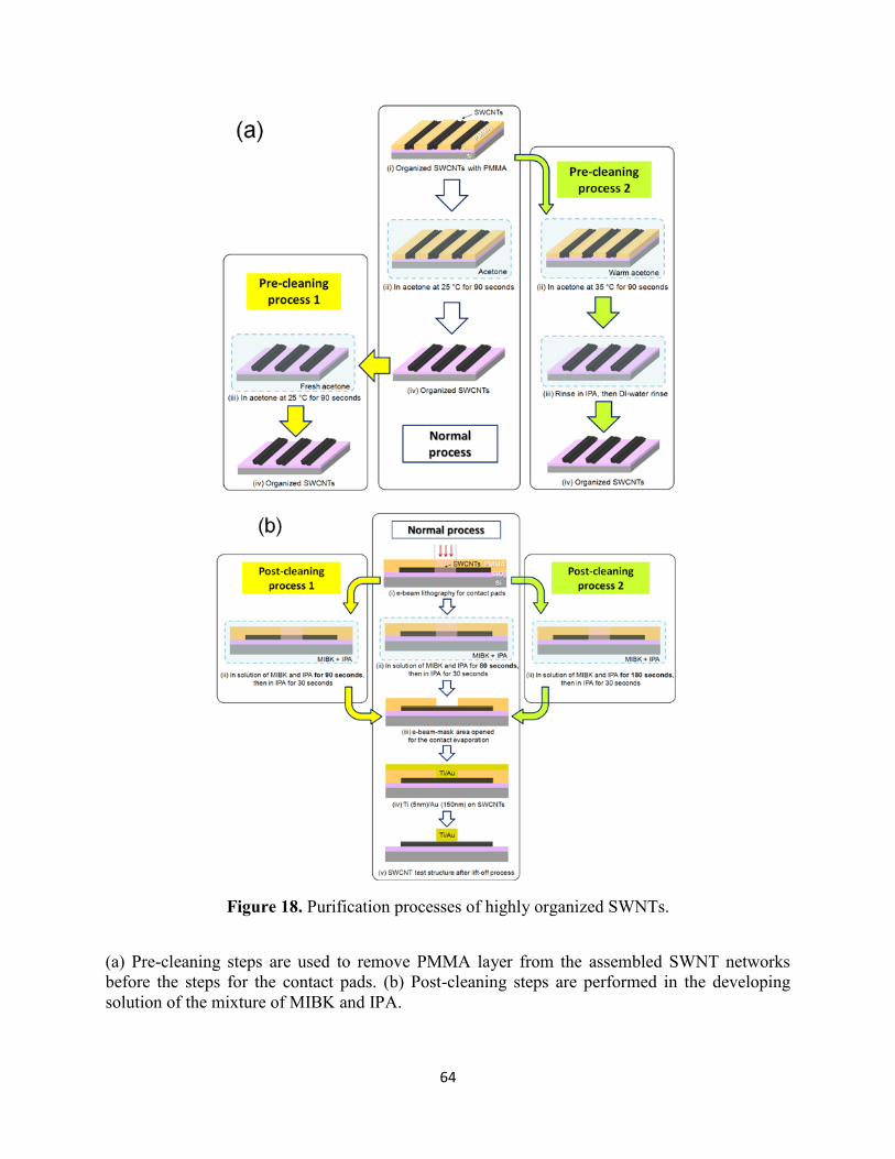
64
Figure 18. Purification processes of highly organized SWNTs.
(a) Pre-cleaning steps are used to remove PMMA layer from the assembled SWNT networks
before the steps for the contact pads. (b) Post-cleaning steps are performed in the developing
solution of the mixture of MIBK and IPA.

65
wash was performed in warm acetone (at 35°C), and was followed by rinsing in Isopropyl
alcohol (IPA) and DI water.
After the assembled structures have been thoroughly cleaned, they were prepared for contact
fabrication using standard EBL procedures. Then, the “post-cleaning” steps were performed after
the electron beam writing step. Normally, after the writing is performed, the substrates are
immersed in developing solution of the mixture of Methyl isobutyl ketone (MIBK) and IPA
(1:3) for 80 seconds and then rinsed in IPA for 30 seconds (figure 18b). In post-cleaning process
1, the developing time was increased to 90 seconds, whereas in post-cleaning process 2, the
developing time was increased to 180 seconds. The rinsing steps were kept the same, and then
Ti/Au electrodes were coated to form contacts (as described before). The overall two-terminal
resistance in a large number of devices was measured (each type of measurement was done on 5
devices) using the normal and each one of the new cleaning processes. In addition to these
process steps, a fifth process was also developed, which was a combination of pre-cleaning
process 2 and a post-cleaning with an even longer developing time of 210 seconds. Figure 19b
shows an SEM image of the assembled SWNT structures using this last method, where visual
inspection shows removal of all contamination of PMMA. Equation 1 was used to estimate the
contact resistance of the central electrode in each of the cases. Here we compare the average
results of each of the cleaning processes. All other assembly-related parameters were kept
constant.
3.5 Contact Resistance depending on Purification Methods
66
The effect of the second acetone wash (pre-cleaning process 1) can be brought out by
comparing the resistances of the SWNT networks that have been fabricated with and without the
second acetone wash. The overall two-terminal resistances of the SWNT networks which
undergo one and two acetone washes, respectively, were 4403 Ω and 3416 Ω on the average,
showing a decrease of 22.4 % in overall resistance. For the measured value of contact resistance,
this is the contact resistance at one contact, RcB. The contact resistances of their structures were
1025 Ω and 313 Ω on the average, respectively, a decrease of 69.5 % in case of the second
acetone washed devices. Note that this pre-cleaning is effective even though PMMA is coated
once again in both devices for contact fabrication. This clearly brings out that PMMA
contamination during the first acetone wash is more severe compared to any surface-adhesion
during the spin-coating step of the second PMMA layer. As we will see later, this pre-cleaning
step is crucial for obtaining lower contact resistances in these structures.
To compare the effects of post-cleaning, the pre-cleaning acetone wash was fixed at 180
seconds. For 90 seconds and 180 seconds development in the mixture of MIBK and IPA, the
overall SWNT network resistances were 1898 Ω and 1530 Ω on the average, respectively,
indicating a decrease of 19.4 % in overall resistance. The contact resistances, RcB, of their
structures were 462 Ω and 259 Ω on the average, respectively, a decrease of 43.9 % in contact
resistance with 180 seconds developing treatment. This clearly showed that the post-cleaning
step was also very important in removing residual PMMA from the SWNT networks.
In order to optimize the cleaning process, various combinations of pre- and post-cleaning
steps were investigated, and the lowest contact resistance was obtained when the pre-cleaning
process 2 was combined with a 210 seconds post-cleaning MIBK development time. Under this
combination of steps, the average overall resistance and contact resistances (RcB) were 1776 Ω

67
Figure 19. Electrical properties and SEM images of SWNT structures depending on the
treatment of cleaning.
(a) SEM image is for a typical surface of SWNTs after the first acetone wash for 90 seconds,
showing the residues of PMMA. (b) Typical SEM image for the surface of SWNTs with warm
acetone, IPA, and 210 seconds developing time, showing a clean surface. (c) Overall resistances
according to the cleaning methods. (d) Their contact resistance in overall resistance. This is the
value at the central lead (B) (see text).
and 15 Ω, reflecting a decrease by 59.7 % and 98.5 %, respectively, compared to the SWNT
networks that underwent only the first acetone wash treatment i.e., the contact resistance was
enormously reduced using this procedure. Figure 19c and 19d plot the average overall and
contact resistances at the central lead (B) for SWNT networks which have undergone different
cleaning procedures. Note that compared to the original method, the optimal method has a
contact resistance which is very close to zero.
68
To conclusively establish that the resistance change was occurring only at the interface
between the SWNT networks and the metal contact, we also performed a control experiment that
studied the effect of acetone treatment on the contact resistance after putting contact leads. It
details the overall and contact resistances in SWNT networks that undergo one wash (normal),
and compares them to SWNT networks which are washed a second time after the metal
electrodes were fabricated (i.e. the contact area was covered with metal), keeping all other steps
identical. It was found on an average that the overall resistance varied only within 6.8 %, with no
clear decreasing trend. In fact, the contact resistance increased by a few percents in some cases.
This result clearly shows that cleaning the contact area before metallization is crucial in lowering
both the contact and overall resistance of SWNT network interconnects, and that the decrease of
contact resistance is not due to any doping effects from acetone.
We next look at the average percentage contribution of the contact resistance to the average
overall two-terminal resistance of our SWNT interconnects at the end of each cleaning process
steps. Figure 20 summarizes these data. We note that the percentage of the contact resistance has
been calculated taking both contacts into account, assuming that the second contact has an
identical contact resistance. We find that in all cases, the contact resistances decrease
significantly after second treatment except for the control experiment (cleaning after contact pads
were fabricated). In the controlled experiment where the second acetone wash was performed
after putting contact metals, the contact resistance did not change much compared to those
SWNT networks that were treated with only the first acetone wash, showing a nominal
difference of 0.65 % (Group number 1). The percentage of contact resistance corresponding to a
developing time of 180 seconds was reduced by 14.82 % (33.86 % compared to the value of
48.68 % for the 90 seconds developing time) (Group number 2). Adding the second acetone

69
Figure 20. Percentage of contact resistance in overall resistance, showing the contact resistances
are decreased according to the different cleaning process.
Group number 1: acetone wash after contact pads, Group number 2: developing time dependence
for contact pad fabrication, Group number 3: acetone wash before contact pads, Group 4: warm
acetone + IPA + 210 seconds developing (see text). This percentage has been calculated taking
BOTH contacts into account, assuming the second contact has an identical contact resistance. A
second acetone wash and more developing time to the SWNT device play an important role in
reducing its interfacial contact resistance.
wash before putting contact pads reduced the contact resistance from 46.56 % to 18.33 %,
decreasing by 28.23 % (Group number 3). However, the best results were clearly obtained by
using a combination of warm acetone (second wash) and IPA and 210 seconds developing time,
whereby the average percentage of contact resistance was reduced to 1.69 % of the overall
resistance of SWNT networks (Group number 4). We note that in some cases, the contact
resistance was found to be below 1% of the overall resistance, which we consider to be below are
experimental error limit. Hence, we find that the optimal cleaning procedure described above can

70
lower the contact resistance to lower values compared to the average contact resistance of 48.67
% for in normal SWNT architectures, approaching values which are very low within our
experimental accuracy.
3.6 Dependence of Contact Resistance on Temperature
Under real operations, interconnects in microprocessors are known to work at elevated
temperatures, and hence we also investigated the robustness of the low contact resistance at a
higher temperature of 100 °C and 180 °C (under vacuum) as shown in figure 21 for a typical
device. The contact resistance of this device remained the same at 100 °C, and increased by 1.76 %
at room temperature after one hour annealing at 100 °C. After keeping at 180 °C for one hour,
the percentage of contact resistance reduced again by 0.8 % compared to the previous room
temperature value. These measurements indicate that the change of contact resistances is within
2 %, demonstrating their robustness against realistic operational temperatures over hours of
operation.
3.7 Conclusions
In summary, a simple and scalable set of extra cleaning steps has been developed that reduces
interfacial contact resistances to values below 2 % of the total SWNT network resistance. The
significant decrease due to additional pre-cleaning establishes clearly that surface contamination
during the first acetone wash is much more detrimental than that which occurs during the second
PMMA spin-coating step, and hence the pre-cleaning process is vital in our method. The post-

71
Figure 21. Change of contact resistance depending on temperatures.
The change of percentage of contact resistance in overall resistance depending on temperature
shows that the variation is within 1.76 %. The contact between highly organized SWNTs and
electrical contact electrodes has a stable ohmic contact with maintaining lower contact resistance.
cleaning step of additional developing time was found to be extremely effective in removing any
surface contamination during the second PMMA coating step. With optimal cleaning conditions
using warm acetone, IPA, and longer developing time, the contact resistance can get as low as 11
Ω which is just 0.74 % of the overall resistance in our SWNT network interconnect test structure,
and is comparable in value with that of the nanoscale metal electrodes. Moreover, the contact
resistance remains in very little change even after hours of heating at temperatures up to 180 °C.

72
Controlled experiments performed after the metal electrodes were deposited showed very little
change in contact resistance, indicating that the entire “decreased” contact resistance pertains to
impurity removal at the nanotube-metal interface, and is not any extraneous effects such as
doping, etc. The enormous decrease of contact resistance in highly organized SWNT networks
demonstrates a big step towards their integration into existing CMOS platforms as future
interconnects.

73
Chapter 4: Chemical Sensor Based on Highly Organized SWNT Networks for
Hydrogen Sulfide
4.1 Introduction
Recently there has been significant interest in using carbon based nanomaterials as chemical sensors
due to several advantages of nanostructured carbon such as light weight, high electrical conductivity,
electrochemical surface area and superior sensing performance. Particularly, CNTs are a growing demand
due to their high electron mobility and large current capability, which on one hand can potentially help in
reducing power consumption of the sensor whereas, on the other hand high temperature stability and
chemical inertness of CNTs may provide a stable and robust platform to detect specific gas [85-91].
Since pristine CNTs based chemical sensors utilize their intrinsic electrochemical properties, to
overcome their limitations in selectivity and sensitivity the most promising approach is to functionalize
CNTs with covalent or non-covalent materials [92, 93]. However owing to their one-dimensional
nanostructure CNTs are highly sensitive to environment such as humidity and temperature [94, 95], in
practice the effect of the relative humidity (RH) in CNT based chemical sensors must be investigated
further because the humidity varies greatly depending on the season, region and weather.
Un-functionalized SWNT based two terminal as well as field effect devices have been
proposed and fabricated for sensing gases like alcohols [96], hydrogen sulfide (H2S) [97],
ammonia [98], nitrogen dioxide [99] etc. However, due to different redox properties of these
gasses, it is difficult to understand the exact sensing mechanism that leads to changes in
conduction characteristics of SWNTs. These un-functionalized SWNT sensors are also not
specific. Therefore, for a highly sensitive chemical sensor with very high specificity,

74
functionalized SWNTs have to be utilized. In order to increase the specificity of SWNTs based
chemical sensors, SWNTs decorated or functionalized with different sensory molecules or
nanoclusters as sensory elements can be employed. Complex as well as simple molecules can be
attached to SWNT surface to alter their properties by the formation of charge transfer complex or
by redox reactions occurring in the close proximity of SWNTs.
H2S is a deadly gas which causes asphyxiation, lung damage, and teratogenic effects when
exposed to it [100, 101]. Thus the monitoring and elimination of H2S is very important for safety
because this gas is found widely in industry such as natural gas, petroleum and mines, and is
given off as a by-product in the manufacture of rayon, synthetic rubber, dyes and the tanning of
leather [102]. So far wide varieties of inorganic and organic materials such as tungsten oxide, tin
oxide and carbon have been proposed as electrical sensors that can detect the H2S gas [103-109].
Although there are several successful devices available commercially, drawbacks of existing H2S
monitors include high power consumption, high operating temperatures, short lifetime,
interference from other gases and high cost [110].
4.2 Fabrication of SWNT Networks for Sensors
We developed template-guided directed fluidic assembly process for fabricting high density
SWNT highly organized structures and networks [32, 34, 111] described in chapter 1.4. Figure
16 shows typical SWNT lateral structures fabricated by the template-guided fluidic assembly of
SWNTs. Figure 16 a and 16b show highly dense and assembled SWNTs line structures in the
low and high magnification of a channel of approximately 1µm. Figure 22 shows the SWNT-
based sensor devices with wire bonding to reduce the electrical noise from ambient environments

75
and vibrations. Figure 22a and 22b show SEM images with a wire bonding process in the overall
structure and individual test structure, respectively. However, as shown in Figure 22c, the SWNT
chemical sensor can be damaged due to the electrostatic discharge (ESD) or thermal oxidation of
SWNTs during the wire bonding process. In order to solve this problem, a new design of metal
contact pads was implemented in which the contact pads were placed far away from the SWNT
sensor as shown in Figure 22d such that ESD or oxidation would not affect SWNT sensing
platforms during wire-bonding. With this new design of contact pads, the SWNTs chemical
sensors were quite stable in the H2S gas testing.
4.3 Non-covalent Functionalization of SWNTs
This covalent functionalization can be effectively achieved in two ways. (i) Creating a defect
site on SWNTs followed by addition of the desired functional groups at the defect site. (ii)
Utilizing carboxylic acid, aldehyde or alcohol functionalities that are already present on the
sidewall of SWNTs as a result of oxidation processes used in SWNT purification. However,
covalent functionalization of SWNTs not only changes the electronic properties of SWNTs
(because of the defects) but also affects chemical, thermal, and mechanical stability of SWNTs
and hence not desirable in developing electronic sensor application which should be used in
harsh environments. To overcome drawbacks of covalent functionalization, researchers have
widely investigated non-covalently functionalized SWNTs. Various species of polymers,
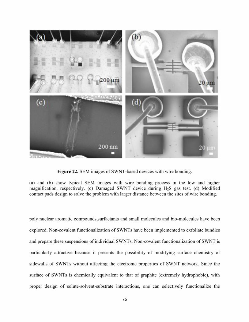
76
Figure 22. SEM images of SWNT-based devices with wire bonding.
(a) and (b) show typical SEM images with wire bonding process in the low and higher
magnification, respectively. (c) Damaged SWNT device during H2S gas test. (d) Modified
contact pads design to solve the problem with larger distance between the sites of wire bonding.
poly nuclear aromatic compounds,surfactants and small molecules and bio-molecules have been
explored. Non-covalent functionalization of SWNTs have been implemented to exfoliate bundles
and prepare these suspensions of individual SWNTs. Non-covalent functionalization of SWNT is
particularly attractive because it presents the possibility of modifying surface chemistry of
sidewalls of SWNTs without affecting the electronic properties of SWNT network. Since the
surface of SWNTs is chemically equivalent to that of graphite (extremely hydrophobic), with
proper design of solute-solvent-substrate interactions, one can selectively functionalize the
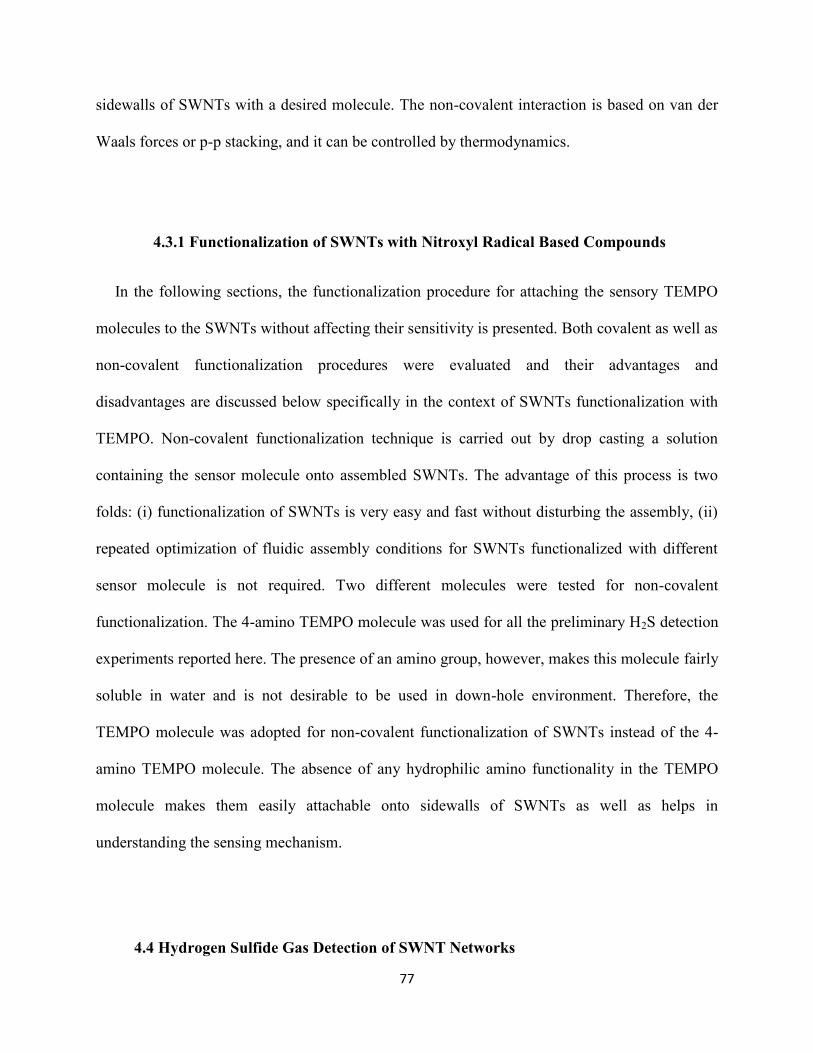
77
sidewalls of SWNTs with a desired molecule. The non-covalent interaction is based on van der
Waals forces or p-p stacking, and it can be controlled by thermodynamics.
4.3.1 Functionalization of SWNTs with Nitroxyl Radical Based Compounds
In the following sections, the functionalization procedure for attaching the sensory TEMPO
molecules to the SWNTs without affecting their sensitivity is presented. Both covalent as well as
non-covalent functionalization procedures were evaluated and their advantages and
disadvantages are discussed below specifically in the context of SWNTs functionalization with
TEMPO. Non-covalent functionalization technique is carried out by drop casting a solution
containing the sensor molecule onto assembled SWNTs. The advantage of this process is two
folds: (i) functionalization of SWNTs is very easy and fast without disturbing the assembly, (ii)
repeated optimization of fluidic assembly conditions for SWNTs functionalized with different
sensor molecule is not required. Two different molecules were tested for non-covalent
functionalization. The 4-amino TEMPO molecule was used for all the preliminary H2S detection
experiments reported here. The presence of an amino group, however, makes this molecule fairly
soluble in water and is not desirable to be used in down-hole environment. Therefore, the
TEMPO molecule was adopted for non-covalent functionalization of SWNTs instead of the 4-
amino TEMPO molecule. The absence of any hydrophilic amino functionality in the TEMPO
molecule makes them easily attachable onto sidewalls of SWNTs as well as helps in
understanding the sensing mechanism.
4.4 Hydrogen Sulfide Gas Detection of SWNT Networks
78
Non-covalently functionalized SWNT devices were exposed to H2S gas under normal
atmospheric conditions as well as under controlled environments. The general term “Response
Time” used for other similar sensors is used here to define the comparison of detection
characteristic of the sensors in various environments. Response time is defined as the time period
in which the detector output signal is reduced to 90% of the initial value. Since the SWNT
chemical sensor’s current is measured for a constant applied voltage as function of time, the
response time in such a case is taken as the time period the sensor takes to drop 10% of the initial
current value as shown schematically in the Figure 23. A larger response time indicates that the
sensor is not highly sensitive whereas a shorter response time indicates a highly sensitive sensor.
The tests were carried out in a glass chamber designed for these tests as shown in Figure 24. In
the following comparisons the response time measured in air was taken as a reference for
different concentrations of H2S gas. Also, all of the data shown in the following sections was
obtained using SWNT devices functionalized using the TEMPO molecule.
4.4.1 Detection of Hydrogen Sulfide in Air
Any sensor usually has an optimal working range for analytic concentrations. This optimal
concentration range defined for a given sensor in a given environment allows one to calibrate the
sensor and detect unknown concentrations. Thus, in order to investigate the optimal working
range for our sensor, we exposed the sensor to different concentrations of H2S gas ranging from
10-1500 ppm. The applied bias voltage was kept constant for every measurement and changes in
current were monitored as a function of time for different gas concentrations. The glass chamber
was kept closed until the current decreased to 10% of its original value. Once the current

79
Figure 23. Shown schematically is the definition of the “Response Time” for an electrical sensor.
Figure 24. Glass chamber setup for controlled environment measurements.
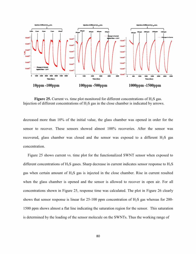
80
Figure 25. Current vs. time plot monitored for different concentrations of H2S gas.
Injection of different concentrations of H2S gas in the close chamber is indicated by arrows.
decreased more than 10% of the initial value, the glass chamber was opened in order for the
sensor to recover. These sensors showed almost 100% recoveries. After the sensor was
recovered, glass chamber was closed and the sensor was exposed to a different H2S gas
concentration.
Figure 25 shows current vs. time plot for the functionalized SWNT sensor when exposed to
different concentrations of H2S gases. Sharp decrease in current indicates sensor response to H2S
gas when certain amount of H2S gas is injected in the close chamber. Rise in current resulted
when the glass chamber is opened and the sensor is allowed to recover in open air. For all
concentrations shown in Figure 25, response time was calculated. The plot in Figure 26 clearly
shows that sensor response is linear for 25-100 ppm concentration of H2S gas whereas for 200-
1500 ppm shows almost a flat line indicating the saturation region for the sensor. This saturation
is determined by the loading of the sensor molecule on the SWNTs. Thus the working range of

81
Figure 26. Shown is a plot of Response time vs Concentration of H2S gas clearly revealing the
working range and saturation region for the functionalized SWNT sensor.
the SWNTs can be changed and expanded by altering the loading of the sensor molecule
resulting in a versatile fabrication procedure for sensor device.
4.4.2 Detection of Hydrogen Sulfide with Metallic/Semiconducting SWNTs in
condition of Water Vapor
In the previous section, we used a mixture of metallic and semiconducting SWNTs for the
devices. Here, we report for the first time molecular doping of 2,2,6,6-Tetramethylpiperidine-1-
oxyl (TEMPO) as a catalyst on the surface of metallic/semiconducting SWNTs and the effective

82
detection of H2S gas by a redox reaction at room temperature. We will also discuss the important
role of water vapor on the electrical conductivity of SWNTs during the sensing of H2S
molecules.
Figure 27 depicts a device schematic and the behavior of H2S and H2O molecules on SWNTs
functionalized with TEMPO molecules. SWNTs serve as an active channel layer because of their
ultra-high surface area to volume ratio and no chemical interaction with H2S or other gases that
may interfere. Especially, semiconducting SWNT (s-SWNT) plays a major role in gas detection
due to their different redox properties [112, 113]. In order to investigate H2S sensing on SWNTs
with different electronic structures (semiconducting and metallic), we performed a controlled
experiment where, 99% purity of metallic SWNT (m-SWNT) and s-SWNT solutions (purchased
from NanoIntegris Inc.) were drop-casted on each inter-digitated finger electrodes. Then we
deposited TEMPO on the SWNT based devices using a vaporization method to achieve uniform
and thin coating for the functionalization of SWNTs, which was then carefully outgassed by
joule heating under 10-3
torr for 1hr followed by injection of dry N2 gas in a sensing chamber.
Since TEMPO possesses stable nitroxyl group provided by the adjacent four methyl groups, it
has widely been used as a radical trap, as a structural probe for biological systems, as a reagent in
organic synthesis, and as a mediator in controlled free radical polymerization [114-116]. Thus it
is also capable of oxidizing the gaseous H2S and can be utilized as a sensory molecule for
making a chemical sensor to detect H2S. Non-covalently functionalized SWNT devices were
exposed to H2S gas under dry N2 or controlled water vapor. Clearly, in all the above-mentioned
detections, the sensing materials come in contact with either H2O or H2S or mixtures of these
two.

83
Figure 27. Device schematic and the behavior of H2S and H2O molecules on SWNTs
functionalized by TEMPO.
Figure 28 shows sensing of H2S molecules with SWNT devices and the effect of relative
humidity. In order to investigate exact sensing mechanism and interactions between SWNT-
TEMPO-H2S-H2O, we compared sensor performances under absence or presence of water
between s-SWNT and m-SWNT devices which are functionalized by TEMPO or not. First, to
understand the effects of H2S gas on a bare SWNT, SWNT-based sensor devices without
TEMPO functionalization were exposed to H2S gas of 5, 10, 50, 100, and 200 ppm, respectively
in the chamber with dry N2. For each concentration of H2S, we evaluated sensitivity S defined
by (( ) ) ⁄ , where is the initial current in dry N2 and is the changed
current after injection of H2S gas. Figure 28a shows the sensitivity of bare s-SWNT device with
H2S concentration in dry N2 (see Appendix A figure S1 for real time current change). Sensitivity
at 200 ppm of H2S shows 38 % change. However, bare m-SWNT device shows less than 5 %
sensitivity (Appendix A figure S2) on detecting H2S gases. This result is consistent with previous
reports [90], indicating more redox properties of the s-SWNTs.

84
Figure 28. Sensitivity and real-time current measurements for detection of H2S gas.
(A) Sensitivity of a bare s-SWNT device as a function of H2S concentration. Real-time current
measurement of (B) a bare s-SWNT device and (C) a device functionalized with TEMPO as a
function of RH. (D) Sensitivity of B and C. In the range of current reduction of B and C, red and
green area mean injection of H2S and H2O molecules respectively, and increase of current
indicates recovery into the initial current value of each RH.
To investigate the effect of H2O on sensing of H2S molecules, we used only 100 ppm
concentration of H2S since it is known that, above that concentration, the human olfactory nerve
can be paralyzed in a few inhalations. Then sensing of H2S gas was performed under different
RH. Figure 28b shows the real-time current changes in a bare s-SWNT device when 100 ppm
H2S gases were exposed at RH of 0, 20, 40 and 60 % (see Appendix A figure S3 for more details
and Appendix A figure S4 for bare m-SWNT device). First, we observed that the current in s-

85
SWNT device decreased when exposed to water vapor. Then a further substantial reduction in
conductance was observed when H2S gas was introduced in the presence of predetermined RH.
After each sensing test under a given RH, the chamber was exposed to dry N2 for the sensor
recovery for sensing of H2S in increased RH. The real-time current measurements clearly
demonstrate that redox properties do change in the presence of H2S and water vapor. The
sensitivity of bare s-SWNT devices was increased significantly to 150% at 60% RH (figure 28d).
H2O molecules can be adsorbed on the surface of SWNTs and act as electron donors in a p-
type semiconductor reducing the hole density in s-SWNTs resulting in the current decreases [94].
This fact is consistent with the initial current drop observed when only water vapor was
introduced as shown in the figure 28b and Appendix A figure S5. To explain the increased H2S
sensitivity of s-SWNT, the interaction of H2S and H2O molecules is a possible subset. H2S is
slightly soluble in water (its solubility is about 3.8 g per kg in water) and acts as a weak acid.
The concentration of 60 % RH at 20 °C is about 38000 ppm, which is enough to dissolve the 100
ppm of H2S. Therefore, the conductance after injection of H2S gas can be changed significantly
by hydrosulfuric acid formed by water molecules attached on the surface of s-SWNTs. This fact
indicates moisture is one of important factors in practical applications and sensitivity of the
chemical sensors.
To maximize sensitivity based on the above facts, TEMPO was used as a homogeneous catalyst
for redox reaction of H2S and H2O. As shown in figure 28c and 28d (see Appendix A figure S6
for more details), s-SWNT devices functionalized with TEMPO showed 420 % sensitivity at 60
% RH, which is about 3 times higher than bare s-SWNT sensor at the same RH, and 17 times
higher than bare s-SWNT device under dry N2 condition.
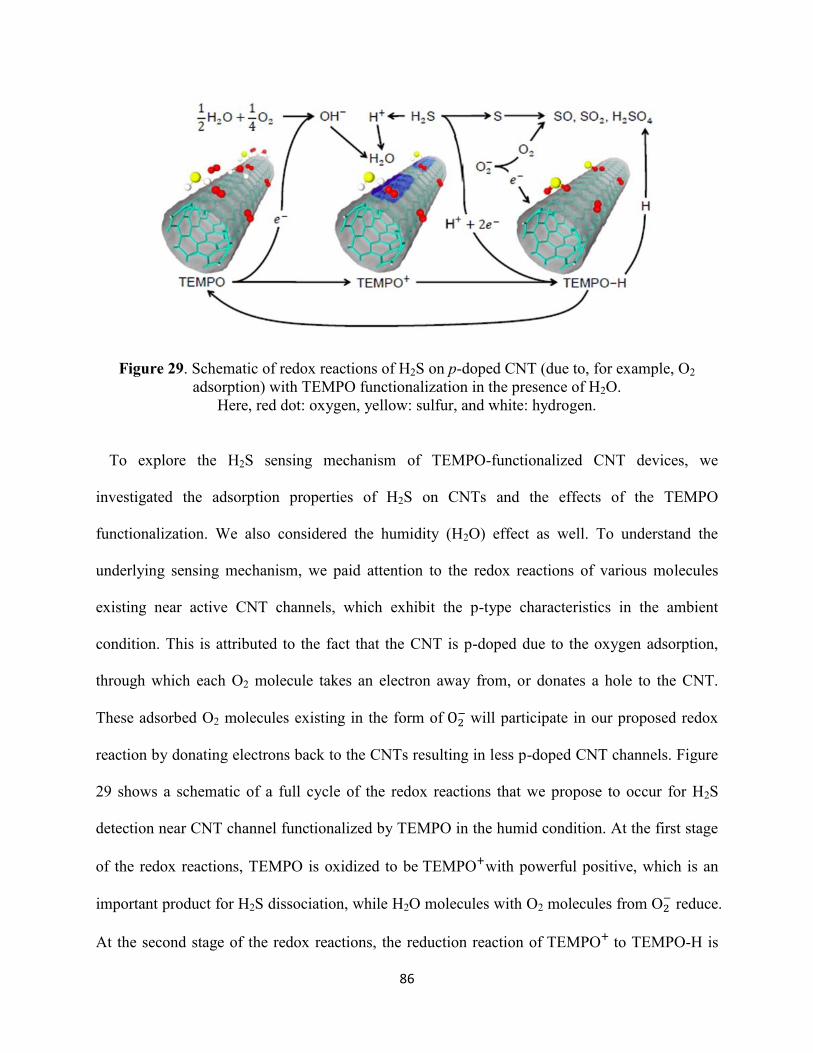
86
Figure 29. Schematic of redox reactions of H2S on p-doped CNT (due to, for example, O2
adsorption) with TEMPO functionalization in the presence of H2O.
Here, red dot: oxygen, yellow: sulfur, and white: hydrogen.
To explore the H2S sensing mechanism of TEMPO-functionalized CNT devices, we
investigated the adsorption properties of H2S on CNTs and the effects of the TEMPO
functionalization. We also considered the humidity (H2O) effect as well. To understand the
underlying sensing mechanism, we paid attention to the redox reactions of various molecules
existing near active CNT channels, which exhibit the p-type characteristics in the ambient
condition. This is attributed to the fact that the CNT is p-doped due to the oxygen adsorption,
through which each O2 molecule takes an electron away from, or donates a hole to the CNT.
These adsorbed O2 molecules existing in the form of will participate in our proposed redox
reaction by donating electrons back to the CNTs resulting in less p-doped CNT channels. Figure
29 shows a schematic of a full cycle of the redox reactions that we propose to occur for H2S
detection near CNT channel functionalized by TEMPO in the humid condition. At the first stage
of the redox reactions, TEMPO is oxidized to be TEMPO
with powerful positive, which is an
important product for H2S dissociation, while H2O molecules with O2 molecules from O
reduce.
At the second stage of the redox reactions, the reduction reaction of TEMPO
to TEMPO-H is

87
coupled to the dissociation process of H2S to S 2H . At the final stage of the redox
reactions cycle, the sulfur atoms produced by the latter reaction at the second stage react with
oxygen ions (O
) responsible for p-type characteristics of CNT devices and thus form various
sulfuric oxides such as SO, SO2 as the oxidation reaction during which the remaining electrons
are back-donated to the CNT channels being less p-type. In the counter reduction reaction,
TEMPO-H becomes back to TEMPO in the presence of other TEMPO molecules, and the
detached H atoms may be involved in the formation of H2SO4 from the sulfuric oxides. Through
such a complete reactions cycle, the TEMPO molecules together with water play a significant
catalytic role for H2S detection.
4.5 Conclusions
In summary, we have fabricated micron scale SWNT based chemical for the detection of H2S
with detection limit as low as 5 ppms. Several design modifications are implemented to increase
the reliability and yield of the sensors. Fabricated two wire sensors (resistance based) had
resistance values suitable for detecting H2S in ppm range. Non-covalently functionalized SWNT
chemical sensor has been tested for detecting H2S in the environments of Air. Response time was
found to be as low as seconds and is a function of environment and concentration of H2S. Sensor
recovers back to its original conductance when exposed back to the atmosphere. Simple device
fabrication and complete recovery of the sensors shows a path to manufacturing low-cost
effective SWNTs based sensors. To date, application of this phenomenon according to the
relative humidity in gas detection has been less studied. Such a platform can open new
possibilities in development of multi-functional gas senor that can truly act as an “electronic nose”

88
by selectively detecting multiple gaseous species. Our sensors offer promising perspectives for
real-time monitoring of H2S gases with highest sensitivity and low power consumption and
potentially at a low cost. Small size of the system will also allow future integration with low
power microelectronics.

89
Chapter 5: Optoelectronic Properties of Heterojunction between SWNTs and
Silicon
5.1 Introduction
In recent times, there has been a remarkable progress in the development of key photonic
circuit components such as on-chip sources, sub-wavelength manipulators, detectors, storage,
filtering and multiplexing technologies [117-120] that are architecturally compatible with the
conventional Si-based integrated circuit (IC) platform. A successful synergy of the ultra-high-
speed, high-bandwidth, low-loss photonics-based data transfer technology with the speed and
performance of densely integrated, ultrafast electronic logic and memory elements of
conventional integrated circuits [121] could significantly mitigate near- and long-term critical
challenges of delay, bandwidth, and quantum-confinement effects associated with the downward
scaling of conventional ICs [122].
One component which could significantly benefit the integration of photonic and electronic
circuits is a hybrid logic element that can operate with both optical and electronic inputs.
Historically, logic operations in purely electronic circuits are achieved through switching of
field-effect transistors [123]. In contrast, a variety of methods can achieve switching in purely
photonic circuits, ranging from the use of second harmonic generation in non-linear optical
materials [124] to the more recent, opto-mechanical resonance techniques [125]. Given the
technological dissimilarity between electronic and optical logic elements, hybridizing these two
could be quite challenging. One approach would be to develop a new type of device, the logic
90
output of which depends on the logic state of both optical and electronic inputs. In principle, this
could be possible if one could develop a photocurrent-generating device whose output can be
also independently controlled by an external voltage. Conventional semiconductor junction
diodes are used in a variety of operational configurations (e.g. p-n, p-i-n, or Schottky junctions)
for photocurrent generation over a wide spectral range. These junctions are ubiquitously
characterized by exponentially growing forward currents and a bias-independent reverse current.
Under illumination, the reverse currents, while remaining bias-independent, grow linearly with
the incident photon flux. This linearity can last over several decades of incident power, rendering
them excellent for optical power meters. However, in the context of a hybrid integrated circuit,
the absence of a method for voltage-control of photocurrents prevents photoswitches from being
used as logic elements, and remains passive communication-enabling switches. Hence, while
voltage-control of electrical currents has existed for decades, the design of a photocurrent-
generator (e.g. a photodiode) whose photocurrent can be switched using an electrical voltage,
appears to be absent.
In this chapter, we show that heterojunctions of SWNTs form a unique junction with lightly
p-doped Si that can very effectively address this issue. Remarkably large switching of
photocurrents can be obtained due to their low dark currents, low short-circuit photo-currents and
high photocurrent responsivity at low reverse biases. This striking behavior, previously
unreported in SWNT/Si junctions, is understood to be an outcome of three key factors: (a)
SWNTs have a very low density of states (DoS) near their Fermi level, which restricts the
number of carriers that can be injected at this energy level, resulting in the low short-circuit
photocurrent irrespective of the input light power; (b) Unless special care is taken, Si can easily
form surface states and hence get “pinned” [126] to the charge-neutrality level of these states;
91
and (c) the closeness of the work function of SWNTs and the electron affinity of Si, which, in a
Si-pinned junction, allows the Fermi level of SWNTs to lie very close to the conduction band
edge (CBE) of Si, where the photo-excited carriers inject from. These factors, along with the fact
that an external voltage, applied directly to the SWNTs, can very effectively modulate its Fermi
level into regions of high DoS, enable a unique voltage-controllable injection of photo-excited
carriers into SWNTs resulting in the observed voltage-controllable responsivity of these
junctions. Further, the entire fabrication process rests on our previously developed “template-
assisted fluidic assembly” method – one of the few techniques that can achieve wafer-scale
uniform assembly of SWNT mats/belts and other architectures with nanoscale precision [33, 74,
75]. As we show, this enables us to obtain highly reproducible and complex optoelectronic logic
elements.
5.2 Literature Review
5.2.1 Conventional Photodetectors
Semiconductor heterojunction photodetectors are extremely popular due to their broad
spectral responsivity, excellent linearity, high quantum efficiency, and high dynamic range of
operation. In addition, they are highly suitable for scaled-up manufacturing, for example in
arrays of pixels for imaging purposes (e.g. in digital cameras). Numerous semiconductors in a
variety of operational configuration are commonly used to detect and measure electromagnetic
waves over a wide spectral range. For example, GaAs (band gap Eg=1.43 eV), GaN (Eg=3.4 eV),
AlGaN (Eg=3.4–6.1 eV) [127], SiC (Eg= 2.36-3.05 eV) and Si (Eg=1.12 eV) etc. are popular
UV detectors [128] both in the photoconductive as well as photovoltaic modes. Si and Ge
92
(Eg=0.67 eV) are compatible with detection in the visible-NIR regions (above these wavelengths,
pyroelectric and bolometric measurements are favored). In most cases, these materials function
as p-n, p-i-n, or Scottky photodiodes. In a reverse-bias condition, the reverse current saturates
and becomes voltage-independent, and is usually linearly related to the incident photon flux. In
this mode, the junctions are usually quite linear over a large range of incident optical power, and
are excellent for optical power meters.
5.2.2 Optoelectronic Photoswitches
Optoelectronic hptoswiches are key elements of digital optoelectronic circuits that require
high ON/OFF ratios at low optical incident power levels. Devices that can change its current by
orders of magnitude at low incident light powers (resulting in high ON/OFF ratios), potentially
through sharply non-linear responses, are appropriate for photoswitches. The linear
photoresponse in conventional photodiodes and their voltage-independent reverse current results
in low ON/OFF ratios. As a result, the use of photodiodes renders a limitation on the optical
power requirement in optoelectronic integrated circuits. Avalanche photodiodes can overcome
this limitation by operating near breakdown reverse voltages. However, such breakdown
voltages are extremely high, often exceeding 10s to 100s of volts, and are problematic for high-
speed optoelectronic switches due to their high noise and unstable recovery. In this context, a
device which demonstrates a low dark reverse-bias current, and responds with very high reverse
photocurrents (equal or more than the forward bias currents) at very low reverse bias values
would be a very effective photo-switch.
5.2.3 Carbon Nanotubes and CNT-Si Heterojunction based Photo-devices

93
SWNTs are one-dimensional (1D) rolled up sheets of graphene (carbon in sp2 hybridized
sheets) [129]. The chirality [129] of a specific SWNT and its 1D confinement enable a whole
family of SWNTs which can be metallic (i.e. with a zero gap at the Fermi level), or
semiconducting (i.e. with a finite band gap) with a whole range of gap values. MWNTs are
closely related materials with multiple coaxial shells. Over the past years, we have developed a
broad variety of carbon nanotubes, and have also demonstrated a number of their important
electronic [130], optical [131], and thermal properties [132].
The presence of discrete energy levels with poor intra-tube charge-transfer presents itself as a
unique system, especially since it forms a very complex band-alignment when placed in close
proximity of a bulk semiconductor such as Si. This is even more so, since nanotube diameters are
far smaller than typical junction depletion widths, and hence the nanotubes in direct contact with
Si may be almost completely free-carrier depleted. This implies that any photo-excitation could
render near-instantaneous carrier separation across the junctions, with very low thermal or
recombination loss.
The photoresponse properties of SWNT-Si based heterojunctions has been a topic of
enormous interest in recent times due to their potential usefulness in low-cost, intermediate
efficiency (4%-13%) solar cells [133-138]. In all these reports, the dark and photo-induced
current-voltage (IV) curves are similar to those seen in conventional p-n or Schottky barrier
junctions, i.e. a near-exponential forward bias current and a voltage-independent reverse bias
current whose magnitude changes linearly with the incident photon flux. Qualitatively, the
overall behavior of the photo-response in SWNT-Si heterojunctions, hence, is very similar to that
of a Schottky junction as shown in the inset of figure 30c. The dark IVs in SWNT-Si

94
heterojunctions fabricated via a template-guided fluidic assembly method have a similar diode-
like behavior, as seen in the inset of figure 30b.
5.3 Optoelectronic Properties of SWNT-Si Hetrojunction
We has developed a novel template guided fluidic assembly technique for depositing well
controlled SWNT architectures onto Si and SiO2 substrates described in chapter 1.4. A very
important aspect of this technique is that effective micro- and nanoscale patterned SWNT
assembly is accomplished using a simple dry plasma treatment to control the surface property of
silicon or silicon oxide substrates without the need to resort to complex wet chemical
functionalization processes. Figure 30a and 1b show a schematic and a digital image of a typical
test structure prepared to examine the photoresponse in SWNT/Si junctions. For the purpose of
characterization, the SWNT belts were extended well into the bare Si area, such that an incident
light spot could be selectively positioned only on the junction, to avoid the role of contacts.
SWNT belts of various dimensions, with lateral dimensions ranging between millimeters (figure
30b) to sub-micrometer (as shown in the SEM image in figure 30c) were fabricated. The
assembly process allows one to obtain highly aligned SWNTs in the belts for belt widths <1 μm
[75], whereas progressively more random SWNT networks form for structures of larger size.
In the past, SWNT mats/thin films have been extensively used to develop a wide range of
applications including transistors [139-141], flexible electronics [142-144], sensors [86, 145,
146], and transparent conductive films for touch-screen [147-149] and energy [147, 150-154]
technologies. More recently, the photo-response properties of SWNT-Si based heterojunctions
have generated enormous interest for low-cost, intermediate efficiency (4%-13%) solar cells

95
[133-138]. Surprisingly, there has been comparatively little attention so far on the development
of scalable SWNT-based high-performance photon-sensing and photoswitching architectures that
can have a sizable impact on next-generation optoelectronics, with the most promising
architecture being an unpinned SWNT/p:Si junction with a responsivity R~133 mA/W [155]. In
all these architectures, the detailed electronic structure and the effective DoS of SWNT films are
usually ignored, and their photoresponse behavior is often modeled in terms of a metal-
semiconductor “Schottky-barrier” junction, where the SWNTs are treated as passive, transparent
conductive (metallic) electrodes. This is quite consistent with their photocurrent response
behavior, which has been inevitably shown to be reverse-bias independent, as expected for both
Schottky-junction or p-n junction photodiodes/solar cells. In stark contrast, the photocurrents in
our junction depend strongly on the applied reverse bias. Figure 30d shows the dark-and photo-
IV curves in our SWNT/Si junctions, where the reverse-bias photocurrent clearly deviates from
the conventional behavior, with a near-zero short-circuit current (independent of the incident
power, see Appendix B) that sharply rises within a few volts of applied reverse bias. A striking
difference is observed between the nature of the photo-IVs of SWNT/Si and that of a
conventional metal/Si Schottky junction of comparable dimensions, illuminated with the same
light source. The inset of figure 30d shows the photocurrent as a function of reverse bias, as well
as a plot of the calculated number of accessible states as a function of the reverse bias (as
discussed later).
It is well-known that unless adequate care is exercised, the presence of surface states on Si
(arising from dangling bonds or native oxides) can dominate its band-bending process in Si,
resulting in a “pinning” of its Fermi level to the surface-charge-neutrality level, typically located

96
Figure 30. SWNT/Si heterojunction structure and photoresponses.
(a) Schematic and (b) digital photograph of a SWNT/Si heterojunction test-structure (2cm×2cm)
with electrical contacts. (c) Pseudo-colored SEM image of a sub-micron-width fluidically
assembled SWNT belt. (d) Dark and Photo-IV (117μW broadband visible illumination) curves of
a typical SWNT/Si heterojunction. The Photo-IV curve of an Au/Ti/Si junction of similar
dimensions and illumination condition is also shown for comparison of their shapes. Inset:
Comparison of the photocurrent data with an empirical model as described in (e). (e)Schematic
energy-level diagram of Si undergoing photoexcitation, adjacent to the cumulative DoS
(CDoS=Σm,n Dm,n(ε)) of selected d≈1nm SWNTs (with chirality values (m,n) as shown). The
photocurrent due to injected electrons from Si into SWNTs is limited by the number of
accessible states in SWNTs, n[eVr] =∫CDoS(ε)dε, integrated between ε=0 and ε=eVr (Vr =
reverse bias), as shown. The dashed line is a schematic trace connecting the quasi-Fermi levels:
due to photoexcited electrons in Si, and due to the application of a reverse bias in SWNTs. (f)
Broadband responsivity and ON/OFF ratios of the SWNT/Si junction as a function of the reverse
bias. (g) Change in open-circuit voltage under 1μW illumination.
97
about 0.37 eV above its valence band edge. Since SWNT surfaces are chemically inert due to
their well-satisfied chemical bonds within the sp2-hybridized C lattice, the Fermi level in Si is
very likely going to be “pinned” unless its surface is carefully prepared and passivated [156].
Although such a junction is rectifying, the Schottky barrier height is fixed (about 0.8 eV in n:Si,
and ~0.37 eV in p:Si, the so called Bardeen limit [157]). In the absence of any surface/interfacial
gap-states, the Fermi level of unpinned Si aligns itself with that of SWNTs under thermal
equilibrium, forming a Schottky barrier that depends on the work-function (and hence the
position of the Fermi level) of SWNTs. Since the Fermi level of SWNTs (as also in graphene)
can be externally tuned (unlike conventional metals), recent works have exploited unpinned
SWNT/Si and graphene/Si junctions to obtain variable-Schottky-barrier, high performance solar
cells [158], “barristors” [156], and field-effect tunneling transistors [159].
The expected hole Schottky barrier for a completely unpinned SWNT/Si junction is bp ≈ ᵡSi +
Eg - SWNT, where ᵡSi = electron affinity of Si ≈4.05eV, Eg = band gap of Si ≈1.12eV, and SWNT
is the intrinsic work-function of SWNT mats that ranges between 3.7eV to 4.4eV [158]. Hence,
an unpinned SWNT/Si junction can be expected to have a bp > 0.77 eV. In contrast, bp of our
SWNT/Si junctions is about 0.35 eV, close to the Bardeen limit for Si (≈0.37 eV), which
suggests that our SWNT/Si junctions form non-ideal Schottky junctions where the Si energy
levels are pinned to its own surface states. This implies that although the SWNT belts lie in
physical contact with Si, their effective Fermi level of can remain close to its native (free-state)
position, which is close to the conduction band edge (CBE) of Si, since ᵡSi ≈ SWNT. Since
SWNTs have extremely low DoS, D(ε), near their Fermi level (assigned as ε=0), photoexcited
electrons near the CBE find very few accessible states, resulting in the near-zero short-circuit
photocurrent seen in our devices. Moreover, the application of a reverse-bias allows a direct

98
lowering of the effective Fermi level resulting in a voltage-tunable quasi-Fermi level that lies
below the original Fermi level. Hence, under reverse bias, a number of unoccupied states open
up allowing an increased injection of photoexcited electrons to inject in from Si, increasing the
photocurrent. Since the photocurrent is limited by the number of accessible states between the
position of the CBE of Si (near ε=0) and the quasi-Fermi level (at ε=eVr, where Vr is the reverse
bias) in SWNTs, its voltage dependence can also be expected to follow the dependence of the
number of accessible states, n(ε=eVr), where n(ε=eVr) can be obtained by integrating the SWNT
DoS between ε=0 and ε=eVr.
To obtain this trend, we employ a toy model to describe the effective electronic structure of
the SWNT belts. Since the as-received SWNTs had d≈1nm, we assume that the belts contain an
equal distribution of all chiralities (m,n) [8] with d≈1nm. The cumulative DoS (CDoS) of the
SWNT belts can be assumed to be proportional to an equally weighted sum of the individual
DoS [27] of each chiral type, CDoS = Σm,nDm,n(ε). Here, ε=0eV is the Fermi level, assumed to be
the same for all SWNTs for the sake of simplicity. We note that this approach is inadequate for
correctly describing the actual CDoS of our SWNT belts. Obtaining a realistic CDoS of the
SWNT belts is a considerable computational challenge, and is currently beyond our capabilities.
The attempt is to obtain a qualitative understanding of how much the photocurrent could
potentially change as a function of the position of the quasi-Fermi level. Figure 30e shows the
CDoS of SWNTs (obtained by summing the DoS of 22 different chirality values of SWNTs with
d≈1nm as shown) according to our model, as a function of electronic energy, ε. The CDoS has
been placed adjacent to a schematic energy-level diagram of Si near its band gap, with the
SWNT Fermi level in the vicinity of the CBE of Si (as discussed before). Under an applied
reverse bias, the Fermi level and hence the number of electron-occupied states of the SWNT belt

99
moves to lower energies, opening up accessible states for photoexcited electrons to inject from Si
into the SWNTs. From the CDoS, n(Vr) is calculated as
reV
0 n,m
n,mr d)](D[)eV(n . n=n(eVr) has
been plotted in the same figure, as well as in figure 30d inset for comparison. It can be seen that
despite the simple approach of this model, the shape of n=n(eVr) is quite consistent with that of
our experimental photocurrent data, suggesting that the SWNT DoS plays a key role in
determining the photocurrent response in these devices. We believe that a more accurate
description of the CDoS, incorporating the atomistic interaction between SWNT/Si and
SWNT/SWNT junctions (sidewall and end-end) can result in more quantitative insight of the
behavior of these junctions.
Figure 30f shows the variation of photocurrent responsivity R=photocurrent(Iph)/incident
power(P), the electrical ON/OFF ratio IP(V)/IP(V=0) and optical ON/OFF ratio =IP(V)/Idark(V) of
the SWNT/Si junction. Commercial photometers using Si-based photodiodes have responsivities
~ few tens of mA/W in the visible region. In comparison, the maximum responsivity Rmax
obtained at a low reverse bias (-3V) exceeds 1A/W. Although there are a few reports on higher
responsivities obtained in quantum-dot, quantum-well and other novel structures [160-162], the
photocurrent responsivity obtained in our devices stands much higher than most past reports on a
variety of photodetectors those on SWNT/Si junctions [26, 155]. In addition, the response is
completely tunable between 0<R<Imax within using very low voltages, which is extremely useful
for brightness adjustable imaging in variable-light conditions. Further, the low dark current and
the incident power-independent low short-circuit currents coupled with this high responsivity at
V=-3V results in high electrical ON/OFF ratio exceeding 2.5×10⁵, and optical ON/OFF ratios
exceeding 104. Such high current-switching ratios are impossible to conceive in mixed-chirality
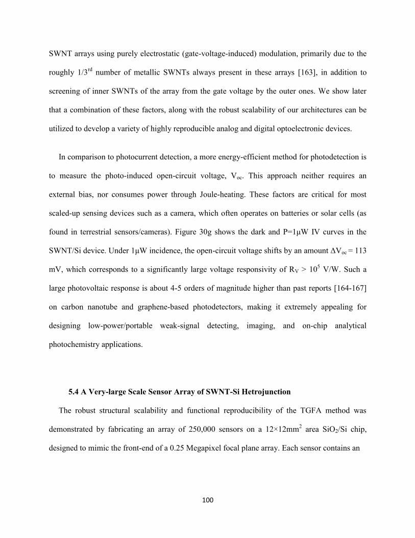
100
SWNT arrays using purely electrostatic (gate-voltage-induced) modulation, primarily due to the
roughly 1/3rd
number of metallic SWNTs always present in these arrays [163], in addition to
screening of inner SWNTs of the array from the gate voltage by the outer ones. We show later
that a combination of these factors, along with the robust scalability of our architectures can be
utilized to develop a variety of highly reproducible analog and digital optoelectronic devices.
In comparison to photocurrent detection, a more energy-efficient method for photodetection is
to measure the photo-induced open-circuit voltage, Voc. This approach neither requires an
external bias, nor consumes power through Joule-heating. These factors are critical for most
scaled-up sensing devices such as a camera, which often operates on batteries or solar cells (as
found in terrestrial sensors/cameras). Figure 30g shows the dark and P=1μW IV curves in the
SWNT/Si device. Under 1μW incidence, the open-circuit voltage shifts by an amount ΔVoc = 113
mV, which corresponds to a significantly large voltage responsivity of RV > 105 V/W. Such a
large photovoltaic response is about 4-5 orders of magnitude higher than past reports [164-167]
on carbon nanotube and graphene-based photodetectors, making it extremely appealing for
designing low-power/portable weak-signal detecting, imaging, and on-chip analytical
photochemistry applications.
5.4 A Very-large Scale Sensor Array of SWNT-Si Hetrojunction
The robust structural scalability and functional reproducibility of the TGFA method was
demonstrated by fabricating an array of 250,000 sensors on a 12×12mm2 area SiO2/Si chip,
designed to mimic the front-end of a 0.25 Megapixel focal plane array. Each sensor contains an

101
Figure 31. Large scale sensor array and photocurrent map.
(a) Digital photograph of a 0.25 Megapixel array of SWNT/Si sensors (array area 12mm×12mm),
shown with increasing levels of magnifications in (b) and (c). (d) SEM image of the “core” of the
sensor, showing a circular window of Si in a SiO2/Si substrate overlaid with SWNTs. Inset: SEM
image of the SWNT packing on Si. (e) Scanning photocurrent map of a 2×2 pixel area of the
sensor array, where the pixels were electrically attached to an external lead, while the back
surface of Si was used as the second contact.
isolated 15×15 μm2 TGFA-assembled SWNT film conformally overlaid onto a 5-μm-diameter Si
window etched out of a 400-nm thick SiO2 layer. Figure 31a-c shows digital photographs of one
such sensor array at different magnification levels, highlighting the fault-free large-scale
integration achievable using our technique. The dense, uniform coverage of the circular Si
window without any stray suspended SWNTs or bubbles as seen in figure 31d is typical for all
areas across the chip, and no structurally defective “sensor” could be found under random SEM

102
inspection of hundreds of sensors over the entire chip. Such a high degree of structural
reproducibility is critical for large-area integration of sensors. We also note that such large-area
uniform integration of high-density SWNT arrays arranged conformally over patterned, uneven
surfaces is quite challenging to implement using conventional SWNT mat-preparation techniques
such as spin-coating [168], drop-casting [169], contact transfer [143], ink-jet printing [170] or
electrospinning [171]. Figure 31d shows a typical scanning photocurrent map of four pixels. We
note that in this case, a background current subtraction was performed. Although each SWNT
film was isolated, the underlying Si is continuous, which resulted in small but finite
photocurrents in a sensor even when the light spot (d≈2.5μm) was a few tens of microns away.
This effect is not expected to appear if the underlying Si is also segmented, as expected in a “real”
device.
5.5 Optoelectronic Logic Devices based on SWNT-Si Hetrojunction
The low dark-current, high photocurrent responsivity and switching ratio obtained at low
reverse-biases, coupled with the robust scalability and compatibility with conventional
semiconductor down-scaling and processing steps of these architectures make these architectures
highly appealing for novel on-chip analog and digital optoelectronic circuitry. The unidirectional
photocurrent (i.e. only in the reverse-bias condition) is easily overcome by defining
“interdigitated” SWNT belts connected to source and drain electrodes as shown in figure 32a. In
this manner, two “back-to-back” photodiodes form a bidirectional phototransistor, as seen from
the dark and photo-IV curve 3b. In darkness, the device remains switched OFF for applied
voltages of either polarity, while under illumination, an ON state can be obtained for both
positive and negative voltages. In this configuration, the device is an optoelectronic equivalent of

103
Figure 32. Phototransistor and AND gate based on SWNT/Si heterojunction.
(a) A bi-directional phototransistor using inter-digitated SWNT fingers attached to source-drain
leads. (b) Typical IV curve obtained in such a device under dark and illuminated conditions
showing photo-induced ON and OFF states. (c) An AND gate with optical and electrical inputs,
and an electrical output. The inset tabulates a typical set of operating conditions determining the
“low” and “high” logic states for both input and output conditions, as determined by the dark and
photocurrents shown in (d). (e) Output of the AND gate for different input logic states as a
function of time.
a symmetric MOSFET, where the gate voltage has been replaced by photons. Further, the
applied voltage and incident light form two independent methods for controlling the channel
current, both of which must be present to obtain an ON state. This feature allows one to construct
a mixed-input optoelectronic AND gate, as described in figure 32c. Here, the light spot incident
on the SWNT/Si junction (input 1 measured in μW) and the applied bias (VIN) are the two logic
inputs, while the measured current output IOUT is the logic output. The optical and electrical ON
-1.0 -0.5 0.0 0.5 1.0-1.5
-1.0
-0.5
0.0
0.5
1.0
1.5
I DS(
A)
VDS
(V)
dark
100 W
-3 -2 -1 010
-9
10-8
10-7
10-6
10-5
10-4
10-3
10-2
Reverse bias (Input 2)
HIGH LOW
HIGH
IOUT
(Output)
LOW
Curr
ent (A
)
Voltage (V)
incident power to device (Input 1)
0 W (LOW)
117 W (HIGH)
-1
0
0
117
0 5 10 15 20
0
-3
[0] [1]IOUT
(100 A)[0] [0] [0] [0]
[1][1]
[1][1] [0][0][0]Input 1
(W)[0]
[0] [0][0]Input 2
(V)
time (s)
[0]
(a) (c)
(b)
(d)
(e)

104
Figure 33. ADDER and 4-BIT optoelectronic D/A converter based on SWNT/Si heterojunction.
(a) Two identically fabricated SWNT/Si structures serving as independent optical inputs for an
optoelectronic ADDER element. Two 650nm LASERs were used to independently address these
two inputs. IOUT is an analog electrical output signal which is proportional to the sum of the two
digital inputs. Depending on the required operational condition, this element also doubles as an
OR gate (see text). (b) IOUT as a function of different input configurations changed as a function
of time. The colored circles indicate the states (ON or OFF) of the two optical inputs. The output
current shows a striking response-reproducibility for independent illumination of the two
structures, as does the current doubling when both inputs are simultaneously illuminated. This
response reproducibility is crucial in designing scalable optoelectronic architectures such as the
4-BIT Optoelectronic D/A converter shown schematically in (c). Here, each successive input has
twice the number of (identical) SWNT belts (see text), corresponding to successive Bit-
significance as shown. (d) Analog current output corresponding to digital optical inputs ranging
from binary 00002 (010) – 11112 (1510).
and OFF states for a typical device can be obtained for the dark and photo-IV curves as shown in
figure 32d, and for convenience, has been tabulated in figure 32c. Figure 32e shows a typical
Inputs ( =OFF =ON)
1
2
0 2 4 6-75
-50
-25
0
I OU
T(
A)
time (s)
Inputs ( =OFF =ON)
20
21
22
23
0 10 20 30 40 50 60-75
-50
-25
0
I OU
T (A
)
time (s)
(a) (b)
(c) (d)

105
time-trace of the output state IOUT, for different logic states of inputs 1 and 2, confirming its
operation as a mixed optoelectronic AND gate.
Due to the highly reproducible responsivity in different junctions fabricated in the same batch,
our “optical input – electronic output” devices are capable of operating with multiple optical
inputs. Figure 33a shows a 2-Bit, digital-input, analog-output ADDER circuit, where the device
performs a dual function of adding two digital input signals and provides an output which is an
analog equivalent of the digital sum. Under appropriate logic conditions, this also serves as an
OR gate, and these operations can be seen in the output time-trace for different input states in
figure 33b. The high-fidelity adding operation can be extended to design more complex input
bits by lithographically designing junctions with highly controlled surface areas. Figure 33c
demonstrates a 4-Bit optoelectronic Digital to Analog converter. To achieve this conversion, 4
separate SWNT/Si junctions, with their junction area proportional to 20,2
1,2
2, and 2
3 were
designed (by fabricating 1,2,4, and 8 parallel identical SWNT belts, respectively) to mimic the
significant bits of a 4-Bit optical input, each of which could be independently illuminated (or
kept dark), resulting in binary inputs, 0000 – 1111. The corresponding output current is
proportional to the analog equivalent of these inputs, as seen in figure 33d. We note that using a
circular laser spot on the parallel SWNT “lines” prevented us from exact area-multiplication.
Nevertheless, we feel that as a proof-of-principle, the analog reproduction of the binary inputs is
quite remarkable.

106
5.6 Conclusions
In summary, we report that the photoresponse of SWNT-Si heterojunctions fabricated using a
template-guided fluidic assembly method shows that a nonlinear reverse bias photocurrent that
increases sharply both with increasing photon flux as well as increasing reverse bias. These
devices possess a radically unconventional photo-response that enables extremely high photo-
induced ON/OFF ratios as high as 104 with responsivity values of ~ 1 A/W as low as -3V.
Remarkably large switching of photocurrents can be obtained due to their low dark currents, low
short-circuit photo-currents and high photocurrent responsivity at low reverse biases. This photo-
response allows us to develop a range of multifunctional optoelectronic switches, photo-
transistors, optoelectronic logic gates and complex optoelectronic digital circuits.

107
Conclusions
In this dissertation, the engineering highly organized and aligned SWNTs has been
demonstrated for electronic devices applications such as interconnects, chemical sensor, and
optoelectronic sensors. Those results were composed of a precisely controlled templated fluidic
assembly technique and their electrical and optical properties based on the devices of SWNTs.
Chapter 1 discussed the electronic structure and properties of SWNTs to understand basic
physics. For 1D system on a cylindrical surface, translational symmetry with a screw axis could
affect the electronic structure and related properties. A fabrication method for micro-to-nano
scale patterned SWNT networks using a newly developed template guided fluidic assembly
process was introduced. A mechanism for SWNT assembly and their control was also described.
In order to maximize the directed assembly efficiency of SWNTs toward a wafer scale SWNT
deposition, SiO2 substrate was treated with controlled plasma treatments. As a result, hydrophilic
chemical groups such as hydroxides were created on the silicon or silicon oxide surface through
the controlled plasma treatment and fluidic SWNT dip-coating process. Nanoscale roughness of
surface structures formed by plasma treatment increased the number of dangling bonds and
hydroxide functional groups on the surface. These combinations of chemical and physical
enhancements attracted SWNTs in the aqueous SWNTs solution. This technique enables us to
make highly organized SWNT networks effectively in various dimensions and geometries.
Moreover, we explored the effect of geometric confinement on the network topology fabricated
by a template-assisted fluidic assembly of SWNT networks. Heterogeneous SWNT networks
became increasingly aligned with decreasing channel width and thickness. Experimental-scale
coarse-grained computations of interacting SWNTs showed that the effect is a reflection of a
108
topology that is no longer dependent on the network density, which emerges as a robust knob
that can induce semiconductor-to-metallic transitions in the network response. In chapter 2, the
nanoscale electrical interconnect test structures constructed from aligned single wall carbon
nanotubes were fabricated and characterized. This process enabled the formation of highly
aligned SWNT interconnect structures on SiO2/Si substrates of widths and lengths that are
limited only by lithographical limits. These structures had high current densities, which was
comparable or better than copper at similar dimensions. The nanotube alignment and failure
current density improved with decreasing width of the structure. We also presented a Pt-
nanocluster decoration method that significantly decreases the resistivity of the structures with a
possible conversion of the semiconducting SWNTs into metallic ones. A method was presented
for significantly reducing the interfacial contact resistance of SWNT interconnect test-structures
in chapter 3. Conventional lithographic cleaning steps remained to large interfacial contact
resistance for the SWNT interconnect structures. With improved cleaning procedures and
controlled experimental methods, the interfacial contact resistance between SWNTs and contact
electrodes of Ti/Au were found to reach values below 2% of the overall resistance of SWNTs.
These results demonstrated the importance of cleaning lithographic residues from the surface of
SWNTs before the fabrication of metal electrodes. These low-resistance contacts are also quite
stable over a large temperature range. In chapter 4, the effective detection of hydrogen sulfide
gas by a redox reaction based on SWNTs functionalized with TEMPO as a catalyst was
introduced. We also discussed the important role of water vapor on the electrical conductivity of
SWNTs during the sensing of H2S molecules. To explore the H2S sensing mechanism, we
investigated the adsorption properties of H2S on CNTs and the effects of the TEMPO
functionalization and we summarized current changes of devices resulting from the redox

109
reactions in the presence of H2S. The semiconducting SWNT device functionalized with
TEMPO showed very high sensitivity of 420 % at 60 % humidity, which is 17 times higher than
a bare s-SWNT device under dry condition. Promising perspectives for personal safety and real-
time monitoring of H2S gases with highest sensitivity and low power consumption and
potentially at a low cost were offered. Chapter 5 introduced optoelectronic devices in fludically-
assembled single walled carbon nanotube/Si heterojunctions. These results showed an
unconventional, voltage-tunable, sharply non-linear and extremely sensitive photo-response in,
with photocurrent responsivity >1A/W, photovoltage responsivity >105 V/W, electrical ON/OFF
ratios > 2.3×10⁵ and optical ON/OFF ratios >10
4. The scalability of our technique was also
demonstrated by fabricating an array of 250,000 micron-scale photo-active junctions covering a
centimeter-scale wafer. Bidirectional phototransistors, and novel logic elements such as a mixed
optoelectronic AND gate, a 2-Bit optoelectronic ADDER/OR gate, and a 4-Bit optoelectronic
D/A converter were also presented. These photocurrent-tunable devices are highly attractive for
low-cost, high-performance on-chip photodetection/imaging, photo-switching, and analog and
digital optoelectronic circuitry.

110
Appendix A
Standard lab preparation of H2S gas molecules
For generation of H2S gas, ferrous sulfide (FeS, purchased from Sigma-Aldrich) was reacted
with sulfuric acid. FeS(s) + H2SO4(aq) → FeSO4(s) + H2S(g). Because H2S gas is denser than air,
it is more convenient to collect it in a glass vial by downward delivery. The gas produced in a
chemical reaction is passed through a delivery tube into the glass vial, where it sinks and pushes
the air out of the top. Calculated volumes of the H2S were then introduced in 1 L of a gas sensing
chamber using a microliter syringe.
Gas detection using SWNTs (w/wo TEMPO) devices
10 mL of 99% pure s-SWNT and m-SWNT solutions (purchased from NanoIntegris Inc.)
were dropcased on interdigitated finger electrodes. The solution was allowed to dry and was
rinsed with water to remove surfactants until maximum current was recorded. After this step, the
devices were exposed to TEMPO vapors for 15 min. The devices were then cooled down at room
temperature and allowed to equilibrate for additional 30 min. For gas sensing, each device was
carefully outgassed by joule heating under 10-3
torr for 1hr in a sensing chamber followed by
flow of dry N2 gas. Gas chamber was then closed and pre-calculated amount of H2S gas was
introduced in it. To understand the effects of concentration of H2S gas, the sensor devices were
exposed to H2S gas of 5, 10, 50, 100, and 200 ppm, respectively in the chamber with dry N2. To
investigate the effect of H2O on sensing of H2S molecules, 100ppm H2S gas was introduced in
the presence of 20, 40 and 60 % RH. Changes in current were observed until it reached
saturation. Once the current saturated, the chamber was exposed to dry N2 for the sensor
recovery.

111
Figure 34. Real time current changes of bare s-SWNT device exposed to H2S gas of 5, 10, 50,
100, and 200 ppm in dry N2.
Figure 35. The sensitivity of a bare m-SWNT device as function of the H2S concentrations in
dry N2.

112
Figure 36. Real-time current measurement of a bare s-SWNT device as a function of RH. The
current reaches almost its saturation value.
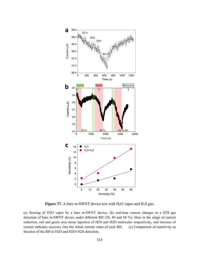
113
Figure 37. A bare m-SWNT device test with H2O vapor and H2S gas.
(a) Sensing of H2O vapor by a bare m-SWNT device, (b) real-time current changes in a H2S gas
detection of bare m-SWNT device under different RH (20, 40 and 60 %). Here in the range of current
reduction, red and green area mean injection of H2S and H2O molecules respectively, and increase of
current indicates recovery into the initial current value of each RH. (c) Comparison of sensitivity as
function of the RH in H2O and H2O+H2S detection.

114
Figure 38. Real-time current drop of the s-SWNT device without TEMPO.
(a) and with TEMPO (b) observed when only water vapor was introduced.
Figure 39. Real-time current measurement of s-SWNT device functionalized with TEMPO as a
function of RH. The current reaches almost its saturation value.

115
Figure 40. A bare m-SWNT functionalized device test with H2O vapor and H2S gas.
(a) Sensing of H2O vapor by a m-SWNT device functionalized with TEMPO, (b) real-time
current changes in a H2S gas detection of the m-SWNT+TEMPO device under different RH (20,
40 and 60 %). Here in the range of current reduction, red and green area mean injection of H2S
and H2O molecules respectively, and increase of current indicates recovery into the initial current
value of each RH. (c) Comparison of sensitivity as function of the RH in H2O and H2O+H2S
detection.

116
Appendix B
Fabrication and optoelectronic properties of SWNT/Si heterojunction
The SWNT solution was obtained from Brewer Science Inc. with the mean length of 610 nm
and mean diameter of 1.1 nm. The solution composed of 0.23 wt % SWNT-DI water solution
(CNTRENETM
C100). A silicon wafer with 400-nm-thick SiO2 layer was obtained from the
University Wafer. Half layer of SiO2 was etched by Buffered Oxide Etch (BOE) 10:1 solution
for 9 min. to expose Si surface to form heterojunction between SWNTs and Si surface. Then, to
improve the contact between the SWNT-deionized water solution and substrate, the substrate
was pretreated using an Inductively-Coupled Plasma (ICP) with mixed gas flow of O2 (20 sccm),
SF6 (20 sccm), and Ar (5 sccm). The substrate was then spin-coated with a photoresist film and
patterned with trenches using an optical lithography. Patterned substrate was vertically
submerged into the SWNT-DI water solution using a dip-coater and gradually lifted from the
solution with a constant pulling speed of 0.1 mm∙min-1
. Two dip-coating processes with 180
degree rotation were applied to make a better coverage of SWNTs along with the trenches. After
this assembly process, a photoresist film was removed in acetone and rinsed in DI water. Then,
the substrate was dried with nitrogen. For electrical characterization, contact pads were
fabricated on the surface of SWNTs and oxide substrate using an optical lithography and Ti (5
nm)/Au (150 nm) deposition followed by a lift-off process. To make Ohmic contact between
Ti/Au and Si surface in area of NO SWNTs, Si surface was scratched gently right before the
deposition of Ti/Au electrodes (see Figure 30(b)). The electrical characterization was conducted
using a Janis ST-500 electrical probe station connected to an Agilent 4156C precision
semiconductor parameter analyzer.
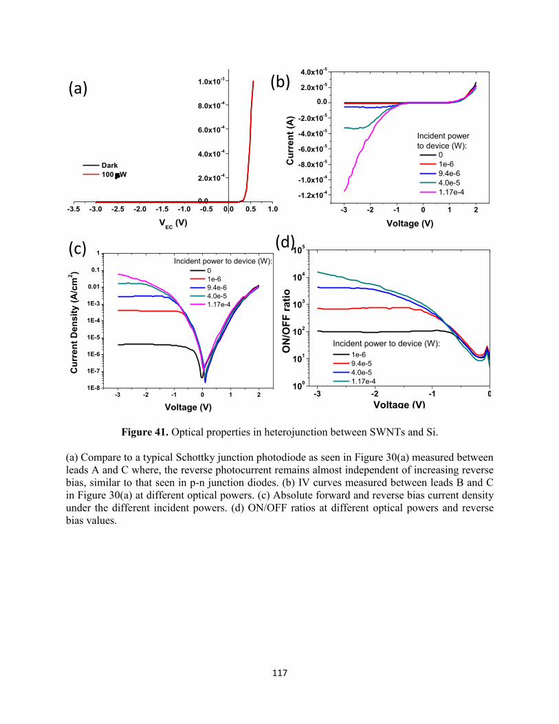
117
Figure 41. Optical properties in heterojunction between SWNTs and Si.
(a) Compare to a typical Schottky junction photodiode as seen in Figure 30(a) measured between
leads A and C where, the reverse photocurrent remains almost independent of increasing reverse
bias, similar to that seen in p-n junction diodes. (b) IV curves measured between leads B and C
in Figure 30(a) at different optical powers. (c) Absolute forward and reverse bias current density
under the different incident powers. (d) ON/OFF ratios at different optical powers and reverse
bias values.
-3.5 -3.0 -2.5 -2.0 -1.5 -1.0 -0.5 0.0 0.5 1.00.0
2.0x10⁻⁴
4.0x10⁻⁴
6.0x10⁻⁴
8.0x10⁻⁴
1.0x10⁻³
VEC
(V)
Dark
100 W
-3 -2 -1 0 1 2
-1.2x10⁻⁴
-1.0x10⁻⁴
-8.0x10⁻⁵
-6.0x10⁻⁵
-4.0x10⁻⁵
-2.0x10⁻⁵
0.0
2.0x10⁻⁵
4.0x10⁻⁵
Cu
rre
nt
(A)
Voltage (V)
0
1e-6
9.4e-6
4.0e-5
1.17e-4
Incident power
to device (W):
-3 -2 -1 0 1 21E-8
1E-7
1E-6
1E-5
1E-4
1E-3
0.01
0.1
1
Cu
rre
nt
De
ns
ity (
A/c
m2)
Voltage (V)
0
1e-6
9.4e-6
4.0e-5
1.17e-4
Incident power to device (W):
-3 -2 -1 010
0
101
102
103
104
105
Incident power to device (W):
ON
/OF
F r
ati
o
Voltage (V)
1e-6
9.4e-5
4.0e-5
1.17e-4
-3.5 -3.0 -2.5 -2.0 -1.5 -1.0 -0.5 0.0 0.5 1.00.0
2.0x10⁻⁴
4.0x10⁻⁴
6.0x10⁻⁴
8.0x10⁻⁴
1.0x10⁻³
VEC
(V)
Dark
100 W
(a) (b)
(c) (d)

118
Fabrication of a very-large scale sensor array of SWNT-Si hetrojunction
The 400-nm thick SiO2 substrate was spin-coated with a photoresist film and patterned with
dot using an optical lithography. With the first mask process, an array of 250,000 holes (500 by
500) on a 12×12mm2 area SiO2/Si chip was made to open the Si surface window for the
assembly of SWNTs. Patterned chip was etched by BOE 10:1 solution for 9 min. to expose Si
surface to form heterojunction between SWNTs and Si surface (see Figure 42(a and b)). Then, to
improve the quality of assembly of SWNTs, the substrate was pretreated using the same plasma
treatment described above. Next, the second mask process was conducted for the SWNTs
assembly followed by another optical lithography (see Figure 42(c and d)). Patterned substrate
was vertically submerged into the SWNT-DI water solution using a dip-coater and gradually
lifted from the solution with a constant pulling speed of 0.1 mm∙min-1
. Four dip-coating
processes with 90 degree rotation each time were applied to make a good coverage of SWNTs
along with the square patterns (see Figure 42(e and f)). After this assembly process, a photoresist
film was removed in acetone and rinsed in DI water. Then, the substrate was dried with nitrogen.
For the metal electrodes, the third mask process was conducted by another optical lithography
to open a boundary area between SWNTs and SiO2 surface (see Figure 43(a and b)). Then,
contact pads were fabricated on the surface of SWNTs and oxide substrate with Ti (5 nm)/Au
(150 nm) deposition followed by a lift-off process (see Figure 43(c and d)). With all mask
processes, an array of 250,000 holes on a 12×12mm2 area SiO2/Si chip, designed to mimic the
front-end of a 0.25 Megapixel focal plane array was fabricated (see Figure 31(a)). Each sensor
contains an isolated 15×15 μm2 assembled SWNT film overlaid onto a 5-μm-diameter Si
window etched out of a 400-nm thick SiO2 layer.
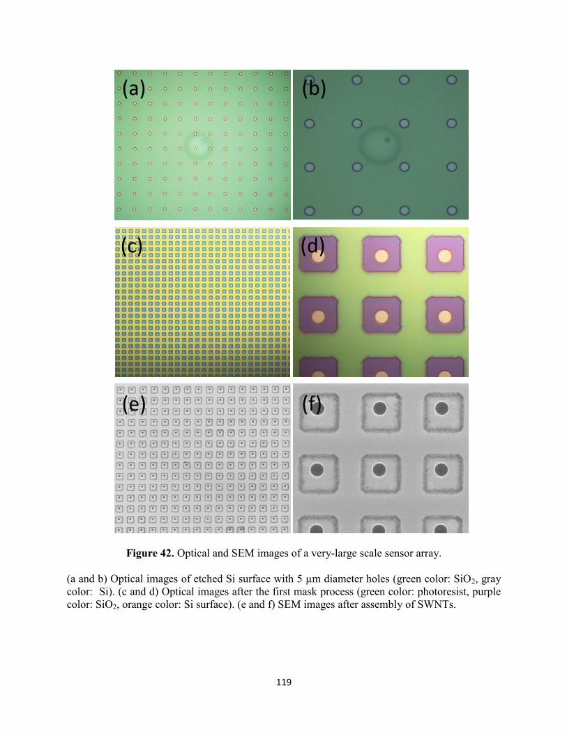
119
Figure 42. Optical and SEM images of a very-large scale sensor array.
(a and b) Optical images of etched Si surface with 5 µm diameter holes (green color: SiO2, gray
color: Si). (c and d) Optical images after the first mask process (green color: photoresist, purple
color: SiO2, orange color: Si surface). (e and f) SEM images after assembly of SWNTs.
(a) (b)
(c) (d)
(e) (f)

120
Figure 43. Optical images of assembled SWNTs and electrodes.
(a and b) Optical images after the second mask process for electrodes (green color: photoresist,
purple color: SiO2, blue color: SWNTs). (c and d) Optical images with electrodes of Ti/Au
(yellow color: Au, purple color: SiO2, assembled SWNTs on holes).
Figure 44. Tested sensor array images for a Raman mapping measurement.
(a) (b)
(c) (d)
(a) (b)

121
Figure 45. G-band intensities using a Raman mapping process corresponding to 2 by 2 sensor
array. These Raman mapping processes were matched in Figure 31(c and e).
1000 1200 1400 1600 1800 2000
1000 1200 1400 1600 1800 2000
1000 1200 1400 1600 1800 2000
Raman Shift (cm-1)
1000 1200 1400 1600 1800 2000
Raman Shift (cm-1)
(a-1) (a-2)
(a-3) (a-4)
(b-1) (b-2)
(b-3) (b-4)
122
Bibliography
[1] D. Bethune, C. Klang, M. De Vries, G. Gorman, R. Savoy, J. Vazquez, and R. Beyers,
"Cobalt-catalysed growth of carbon nanotubes with single-atomic-layer walls," Nature,
vol. 363, pp. 605-607, 1993.
[2] S. Iijima and T. Ichihashi, "Single-shell carbon nanotubes of 1-nm diameter," Nature, vol.
363, pp. 603-605, 1993.
[3] A. Graham, G. Duesberg, W. Hoenlein, F. Kreupl, M. Liebau, R. Martin, B.
Rajasekharan, W. Pamler, R. Seidel, and W. Steinhoegl, "How do carbon nanotubes fit
into the semiconductor roadmap?," Applied Physics A: Materials Science & Processing,
vol. 80, pp. 1141-1151, 2005.
[4] B. Wei, R. Vajtai, and P. Ajayan, "Reliability and current carrying capacity of carbon
nanotubes," Applied Physics Letters, vol. 79, p. 1172, 2001.
[5] M. Dresselhaus, G. Dresselhaus, and R. Saito, "Physics of carbon nanotubes," Carbon,
vol. 33, pp. 883-891, 1995.
[6] D. Bethune, C. Klang, M. De Vries, G. Gorman, R. Savoy, J. Vazquez, and R. Beyers,
"Cobalt-catalysed growth of carbon nanotubes with single-atomic-layer walls," 1993.
[7] S. Iijima and T. Ichihashi, "Single-shell carbon nanotubes of 1-nm diameter," 1993.
[8] M. Dresselhaus and P. Eklund, "Phonons in carbon nanotubes," Advances in Physics, vol.
49, pp. 705-814, 2000.
[9] M. Dresselhaus, G. Dresselhaus, and R. Saito, "Carbon fibers based on C_60 and their
symmetry," Physical Review B, vol. 45, pp. 6234-6242, 1992.
[10] H. Dai, "Carbon nanotubes: synthesis, integration, and properties," Accounts of chemical
research, vol. 35, pp. 1035-1044, 2002.
[11] M. Terrones, "Science and technology of the twenty-first century: synthesis, properties,
and applications of carbon nanotubes," Annual Review of Materials Research, vol. 33, pp.
419-501, 2003.
[12] M. Anantram and F. Leonard, "Physics of carbon nanotube electronic devices," Reports
on Progress in Physics, vol. 69, p. 507, 2006.
[13] N. Hamada, S. Sawada, and A. Oshiyama, "New one-dimensional conductors: Graphitic
microtubules," Physical review letters, vol. 68, pp. 1579-1581, 1992.

123
[14] J. Bernholc, D. Brenner, M. Buongiorno Nardelli, V. Meunier, and C. Roland,
"Mechanical and electrical properties of nanotubes," Annual Review of Materials
Research, vol. 32, pp. 347-375, 2002.
[15] X. Blase, L. X. Benedict, E. L. Shirley, and S. G. Louie, "Hybridization effects and
metallicity in small radius carbon nanotubes," Physical review letters, vol. 72, pp. 1878-
1881, 1994.
[16] Y. K. Kwon and D. Tománek, "Electronic and structural properties of multiwall carbon
nanotubes," Physical Review B, vol. 58, pp. 16001-16004, 1998.
[17] P. Delaney, H. J. Choi, J. Ihm, S. G. Louie, and M. L. Cohen, "Broken symmetry and
pseudogaps in ropes of carbon nanotubes," Nature, vol. 391, pp. 466-468, 1998.
[18] A. Fujiwara, Y. Matsuoka, H. Suematsu, N. Ogawa, K. Miyano, H. Kataura, Y. Maniwa,
S. Suzuki, and Y. Achiba, "Photoconductivity in semiconducting single-walled carbon
nanotubes," Japanese Journal of Applied Physics, 2001.
[19] M. Freitag, Y. Martin, J. Misewich, R. Martel, and P. Avouris, "Photoconductivity of
single carbon nanotubes," Nano letters, vol. 3, pp. 1067-1071, 2003.
[20] D. Stewart and F. Léonard, "Photocurrents in nanotube junctions," Physical review letters,
vol. 93, p. 107401, 2004.
[21] J. Misewich, R. Martel, P. Avouris, J. Tsang, S. Heinze, and J. Tersoff, "Electrically
induced optical emission from a carbon nanotube FET," Science, vol. 300, pp. 783-786,
2003.
[22] A. Hagen and T. Hertel, "Quantitative analysis of optical spectra from individual single-
wall carbon nanotubes," Nano letters, vol. 3, pp. 383-388, 2003.
[23] M. J. O'connell, S. M. Bachilo, C. B. Huffman, V. C. Moore, M. S. Strano, E. H. Haroz,
K. L. Rialon, P. J. Boul, W. H. Noon, and C. Kittrell, "Band gap fluorescence from
individual single-walled carbon nanotubes," Science, vol. 297, pp. 593-596, 2002.
[24] Y. Wang, K. Kempa, B. Kimball, J. Carlson, G. Benham, W. Li, T. Kempa, J.
Rybczynski, A. Herczynski, and Z. Ren, "Receiving and transmitting light-like radio
waves: Antenna effect in arrays of aligned carbon nanotubes," Applied Physics Letters,
vol. 85, pp. 2607-2609, 2004.
[25] K. B. K. Teo, E. Minoux, L. Hudanski, F. Peauger, J. P. Schnell, L. Gangloff, P.
Legagneux, D. Dieumegard, G. A. J. Amaratunga, and W. I. Milne, "Microwave devices:
Carbon nanotubes as cold cathodes," Nature, vol. 437, pp. 968-968, 2005.
[26] J. Wei, J. L. Sun, J. L. Zhu, K. Wang, Z. Wang, J. Luo, D. Wu, and A. Cao, "Carbon
nanotube macrobundles for light sensing," Small, vol. 2, pp. 988-993, 2006.
124
[27] R. Saito, G. Dresselhaus, and M. Dresselhaus, "Trigonal warping effect of carbon
nanotubes," Physical Review B, vol. 61, p. 2981, 2000.
[28] H. Kataura, Y. Kumazawa, Y. Maniwa, I. Umezu, S. Suzuki, Y. Ohtsuka, and Y. Achiba,
"Optical properties of single-wall carbon nanotubes," Synthetic Metals, vol. 103, pp.
2555-2558, 1999.
[29] Y. J. Jung, Y. Homma, T. Ogino, Y. Kobayashi, D. Takagi, B. Wei, R. Vajtai, and P. M.
Ajayan, "High-density, large-area single-walled carbon nanotube networks on nanoscale
patterned substrates," The Journal of Physical Chemistry B, vol. 107, pp. 6859-6864,
2003.
[30] K. Hata, D. N. Futaba, K. Mizuno, T. Namai, M. Yumura, and S. Iijima, "Water-assisted
highly efficient synthesis of impurity-free single-walled carbon nanotubes," Science, vol.
306, pp. 1362-1364, 2004.
[31] K. G. Thomas, S. Barazzouk, B. I. Ipe, S. T. S. Joseph, and P. V. Kamat, "Uniaxial
plasmon coupling through longitudinal self-assembly of gold nanorods," The Journal of
Physical Chemistry B, vol. 108, pp. 13066-13068, 2004.
[32] P. Makaram, S. Somu, X. Xiong, A. Busnaina, Y. J. Jung, and N. McGruer, "Scalable
nanotemplate assisted directed assembly of single walled carbon nanotubes for nanoscale
devices," Applied Physics Letters, vol. 90, p. 243108, 2007.
[33] X. Xiong, L. Jaberansari, M. G. Hahm, A. Busnaina, and Y. J. Jung, "Building Highly
Organized Single‐Walled‐Carbon‐Nanotube Networks Using Template‐Guided Fluidic
Assembly," Small, vol. 3, pp. 2006-2010, 2007.
[34] L. Jaber-Ansari, M. G. Hahm, S. Somu, Y. E. Sanz, A. Busnaina, and Y. J. Jung,
"Mechanism of very large scale assembly of SWNTs in template guided fluidic assembly
process," Journal of the American Chemical Society, vol. 131, pp. 804-808, 2008.
[35] S. Somu, H. Wang, Y. Kim, L. Jaberansari, M. G. Hahm, B. Li, T. Kim, X. Xiong, Y. J.
Jung, and M. Upmanyu, "Topological transitions in carbon nanotube networks via
nanoscale confinement," ACS nano, vol. 4, pp. 4142-4148, 2010.
[36] C. Kocabas, N. Pimparkar, O. Yesilyurt, S. Kang, M. A. Alam, and J. Rogers,
"Experimental and theoretical studies of transport through large scale, partially aligned
arrays of single-walled carbon nanotubes in thin film type transistors," Nano letters, vol.
7, pp. 1195-1202, 2007.
[37] L. Girifalco, M. Hodak, and R. S. Lee, "Carbon nanotubes, buckyballs, ropes, and a
universal graphitic potential," Physical Review B, vol. 62, p. 13104, 2000.
[38] H. Liang and M. Upmanyu, "Elastic self-healing during shear accommodation in
crystalline nanotube ropes," Physical review letters, vol. 94, p. 65502, 2005.

125
[39] M. Islam, A. Alsayed, Z. Dogic, J. Zhang, T. Lubensky, and A. Yodh, "Nematic
nanotube gels," Physical review letters, vol. 92, p. 88303, 2004.
[40] N. L. Michael, C. U. Kim, P. Gillespie, and R. Augur, "Electromigration failure in ultra-
fine copper interconnects," Journal of Electronic Materials, vol. 32, pp. 988-993, 2003.
[41] Q. Huang, C. M. Lilley, and R. Divan, "An in situ investigation of electromigration in Cu
nanowires," Nanotechnology, vol. 20, p. 075706, 2009.
[42] B. Q. Wei, R. Vajtai, and P. M. Ajayan, "Reliability and current carrying capacity of
carbon nanotubes," Applied Physics Letters, vol. 79, p. 1172, 2001.
[43] Y. Homma, T. Yamashita, Y. Kobayashi, and T. Ogino, "Interconnection of
nanostructures using carbon nanotubes," Physica B: Physics of Condensed Matter, vol.
323, pp. 122-123, 2002.
[44] F. Kreupl, A. P. Graham, G. Duesberg, W. Steinhögl, M. Liebau, E. Unger, and W.
Hönlein, "Carbon nanotubes in interconnect applications," Microelectronic Engineering,
vol. 64, pp. 399-408, 2002.
[45] K. H. Koo, H. Cho, P. Kapur, and K. C. Saraswat, "Performance comparisons between
carbon nanotubes, optical, and Cu for future high-performance on-chip interconnect
applications," Electron Devices, IEEE Transactions on, vol. 54, pp. 3206-3215, 2007.
[46] S. Kar, C. Soldano, L. Chen, S. Talapatra, R. Vajtai, S. Nayak, and P. Ajayan, "Lu ttinger
Liquid to Al’tshuler- Aronov Transition in Disordered, Many-Channel Carbon
Nanotubes," ACS nano, vol. 3, pp. 207-212, 2008.
[47] C. Fantini, M. Pimenta, M. Dantas, D. Ugarte, A. Rao, A. Jorio, G. Dresselhaus, and M.
Dresselhaus, "Micro-Raman investigation of aligned single-wall carbon nanotubes,"
Physical Review B, vol. 63, p. 161405, 2001.
[48] H. Gommans, J. Alldredge, H. Tashiro, J. Park, J. Magnuson, and A. Rinzler, "Fibers of
aligned single-walled carbon nanotubes: Polarized Raman spectroscopy," Journal of
Applied Physics, vol. 88, p. 2509, 2000.
[49] T. Mustonen, J. Mäklin, K. Kordás, N. Halonen, G. Tóth, S. Saukko, J. Vähäkangas, H.
Jantunen, S. Kar, and P. M. Ajayan, "Controlled Ohmic and nonlinear electrical transport
in inkjet-printed single-wall carbon nanotube films," Physical Review B, vol. 77, p.
125430, 2008.
[50] C. Kocabas, N. Pimparkar, O. Yesilyurt, S. J. Kang, M. A. Alam, and J. A. Rogers,
"Experimental and theoretical studies of transport through large scale, partially aligned
arrays of single-walled carbon nanotubes in thin film type transistors," Nano Letters, vol.
7, pp. 1195-1202, 2007.

126
[51] Y. Zhou, A. Gaur, S. H. Hur, C. Kocabas, M. A. Meitl, M. Shim, and J. A. Rogers, "P-
channel, n-channel thin film transistors and pn diodes based on single wall carbon
nanotube networks," Nano Letters, vol. 4, pp. 2031-2036, 2004.
[52] A. Vijayaraghavan, K. Kanzaki, S. Suzuki, Y. Kobayashi, H. Inokawa, Y. Ono, S. Kar,
and P. M. Ajayan, "Metal- Semiconductor Transition in Single-Walled Carbon
Nanotubes Induced by Low-Energy Electron Irradiation," Nano Lett, vol. 5, pp. 1575-
1579, 2005.
[53] S. Datta, Quantum transport: atom to transistor: Cambridge Univ Pr, 2005.
[54] A. Naeemi and J. Meindl, "Performance modeling for single-and multiwall carbon
nanotubes as signal and power interconnects in gigascale systems," Electron Devices,
IEEE Transactions on, vol. 55, pp. 2574-2582, 2008.
[55] Chen, L., Ph.D. Thesis, Department of Physics, Applied Physics and Astronomy,
Rensselaer Polytechnic Institute, USA, 2008.
[56] J. E. Fischer, H. Dai, A. Thess, R. Lee, N. M. Hanjani, D. L. Dehaas, and R. E. Smalley,
"Metallic resistivity in crystalline ropes of single-wall carbon nanotubes," Physical
Review-Section B-Condensed Matter, vol. 55, p. 4921, 1997.
[57] J. Hone, M. C. Llaguno, N. M. Nemes, A. T. Johnson, J. E. Fischer, D. A. Walters, M. J.
Casavant, J. Schmidt, and R. E. Smalley, "Electrical and thermal transport properties of
magnetically aligned single wall carbon nanotube films," Applied Physics Letters, vol. 77,
p. 666, 2000.
[58] M. Nihei, A. Kawabata, D. Kondo, M. Horibe, S. Sato, and Y. Awano, "Electrical
properties of carbon nanotube bundles for future via interconnects," Jpn. J. Appl. Phys,
vol. 44, pp. 1626–1628, 2005.
[59] Z. Yao, C. L. Kane, and C. Dekker, "High-field electrical transport in single-wall carbon
nanotubes," Physical Review Letters, vol. 84, pp. 2941-2944, 2000.
[60] Y. Chai, P. C. H. Chan, Y. Fu, Y. Chuang, and C. Liu, "Electromigration studies of
Cu/carbon nanotube composite interconnects using Blech structure," Electron Device
Letters, IEEE, vol. 29, pp. 1001-1003, 2008.
[61] Y. Chai, M. Zhang, J. Gong, and P. C. H. Chan, "Reliability evaluation of carbon
nanotube interconnect in a silicon CMOS environment," pp. 1-5.
[62] T. Yuzvinsky, A. Fennimore, W. Mickelson, C. Esquivias, and A. Zettl, "Precision
cutting of nanotubes with a low-energy electron beam," Applied physics letters, vol. 86, p.
053109, 2005.
127
[63] E. Pop, D. A. Mann, K. E. Goodson, and H. Dai, "Electrical and thermal transport in
metallic single-wall carbon nanotubes on insulating substrates," Journal of applied
physics, vol. 101, p. 093710, 2007.
[64] M. Tsutsui, Y. Taninouchi, S. Kurokawa, and A. Sakai, "Electrical breakdown of short
multiwalled carbon nanotubes," Journal of applied physics, vol. 100, p. 094302, 2006.
[65] J. L. Blackburn, T. M. Barnes, M. C. Beard, Y. H. Kim, R. C. Tenent, T. J. McDonald, B.
To, T. J. Coutts, and M. J. Heben, "Transparent conductive single-walled carbon
nanotube networks with precisely tunable ratios of semiconducting and metallic
nanotubes," ACS nano, vol. 2, pp. 1266-1274, 2008.
[66] A. Kaiser, G. Düsberg, and S. Roth, "Heterogeneous model for conduction in carbon
nanotubes," Physical Review B, vol. 57, p. 1418, 1998.
[67] M. C. Strus, A. N. Chiaramonti, Y. L. Kim, Y. J. Jung, and R. R. Keller, "Accelerated
reliability testing of highly aligned single-walled carbon nanotube networks subjected to
DC electrical stressing," Nanotechnology, vol. 22, p. 265713, 2011.
[68] P. Avouris, Z. Chen, and V. Perebeinos, "Carbon-based electronics," Nature
nanotechnology, vol. 2, pp. 605-615, 2007.
[69] M. Portnoi, O. Kibis, and M. Rosenau da Costa, "Terahertz applications of carbon
nanotubes," Superlattices and microstructures, vol. 43, pp. 399-407, 2008.
[70] Y. Hayamizu, T. Yamada, K. Mizuno, R. Davis, D. Futaba, M. Yumura, and K. Hata,
"Integrated three-dimensional microelectromechanical devices from processable carbon
nanotube wafers," Nature nanotechnology, vol. 3, pp. 289-294, 2008.
[71] C. Hierold, A. Jungen, C. Stampfer, and T. Helbling, "Nano electromechanical sensors
based on carbon nanotubes," Sensors and Actuators A: Physical, vol. 136, pp. 51-61,
2007.
[72] D. Suppiger, S. Busato, and P. Ermanni, "Characterization of single-walled carbon
nanotube mats and their performance as electromechanical actuators," Carbon, vol. 46,
pp. 1085-1090, 2008.
[73] M. S. Fuhrer, B. M. Kim, T. Dürkop, and T. Brintlinger, "High-mobility nanotube
transistor memory," Nano letters, vol. 2, pp. 755-759, 2002.
[74] L. Jaber-Ansari, M. Hahm, S. Somu, Y. Sanz, A. Busnaina, and Y. Jung, "Mechanism of
Very Large Scale Assembly of SWNTs in Template Guided Fluidic Assembly Process,"
J. Am. Chem. Soc, vol. 131, pp. 804-808, 2009.
[75] Y. Kim, B. Li, X. An, M. Hahm, L. Chen, M. Washington, P. Ajayan, S. Nayak, A.
Busnaina, and S. Kar, "Highly Aligned Scalable Platinum-Decorated Single-Wall Carbon
128
Nanotube Arrays for Nanoscale Electrical Interconnects," ACS nano, vol. 3, pp. 2818-
2826, 2009.
[76] X. Xiong, L. Jaberansari, M. Hahm, A. Busnaina, and Y. Jung, "Building Highly
Organized Single-Walled-Carbon-Nanotube Networks Using Template-Guided Fluidic
Assembly," Small, vol. 3, pp. 2006-2010, 2007.
[77] L. Chico, L. X. Benedict, S. G. Louie, and M. L. Cohen, "Quantum conductance of
carbon nanotubes with defects," Physical Review B, vol. 54, pp. 2600-2606, 1996.
[78] Z. Yao, H. W. C. Postma, L. Balents, and C. Dekker, "Carbon nanotube intramolecular
junctions," Nature, vol. 402, pp. 273-276, 1999.
[79] P. Avouris, "Molecular electronics with carbon nanotubes," Acc. Chem. Res, vol. 35, pp.
1026-1034, 2002.
[80] S. Lee, B. J. Lee, and P. K. Shin2Ã, "Carbon Nanotube Interconnection and Its Electrical
Properties for Semiconductor Applications," Japanese Journal of Applied Physics, vol.
48, p. 5006, 2009.
[81] K. Rykaczewski, M. R. Henry, S. K. Kim, A. G. Fedorov, D. Kulkarni, S. Singamaneni,
and V. V. Tsukruk, "The effect of the geometry and material properties of a carbon joint
produced by electron beam induced deposition on the electrical resistance of a
multiwalled carbon nanotube-to-metal contact interface," Nanotechnology, vol. 21, p.
035202.
[82] A. Bachtold, M. Henny, C. Terrier, C. Strunk, C. Schönenberger, J. P. Salvetat, J. M.
Bonard, and L. Forro, "Contacting carbon nanotubes selectively with low-ohmic contacts
for four-probe electric measurements," Applied Physics Letters, vol. 73, p. 274, 1998.
[83] L. Dong, S. Youkey, J. Bush, J. Jiao, V. M. Dubin, and R. V. Chebiam, "Effects of local
Joule heating on the reduction of contact resistance between carbon nanotubes and metal
electrodes," Journal of Applied Physics, vol. 101, p. 024320, 2007.
[84] Y. Dan, Y. Lu, N. J. Kybert, Z. Luo, and A. T. C. Johnson, "Intrinsic response of
graphene vapor sensors," Nano Lett, vol. 9, pp. 1472-1475, 2009.
[85] M. S. Strano, C. A. Dyke, M. L. Usrey, P. W. Barone, M. J. Allen, H. Shan, C. Kittrell, R.
H. Hauge, J. M. Tour, and R. E. Smalley, "Electronic structure control of single-walled
carbon nanotube functionalization," Science, vol. 301, pp. 1519-1522, 2003.
[86] E. Snow, F. Perkins, E. Houser, S. Badescu, and T. Reinecke, "Chemical detection with a
single-walled carbon nanotube capacitor," Science, vol. 307, pp. 1942-1945, 2005.
129
[87] H. J. Song, Y. Lee, T. Jiang, A. G. Kussow, M. Lee, S. Hong, Y. K. Kwon, and H. C.
Choi, "Self-clusterized glycines on single-walled carbon nanotubes for alcohol sensing,"
The Journal of Physical Chemistry C, vol. 112, pp. 629-634, 2008.
[88] X. Tang, S. Bansaruntip, N. Nakayama, E. Yenilmez, Y. Chang, and Q. Wang, "Carbon
nanotube DNA sensor and sensing mechanism," Nano letters, vol. 6, pp. 1632-1636,
2006.
[89] T. Kawano, H. C. Chiamori, M. Suter, Q. Zhou, B. D. Sosnowchik, and L. Lin, "An
electrothermal carbon nanotube gas sensor," Nano letters, vol. 7, pp. 3686-3690, 2007.
[90] D. R. Kauffman and A. Star, "Carbon nanotube gas and vapor sensors," Angewandte
Chemie International Edition, vol. 47, pp. 6550-6570, 2008.
[91] M. C. McAlpine, H. Ahmad, D. Wang, and J. R. Heath, "Highly ordered nanowire arrays
on plastic substrates for ultrasensitive flexible chemical sensors," Nature materials, vol. 6,
pp. 379-384, 2007.
[92] M. K. Kumar and S. Ramaprabhu, "Nanostructured Pt functionlized multiwalled carbon
nanotube based hydrogen sensor," The Journal of Physical Chemistry B, vol. 110, pp.
11291-11298, 2006.
[93] A. Star, V. Joshi, S. Skarupo, D. Thomas, and J. C. P. Gabriel, "Gas sensor array based
on metal-decorated carbon nanotubes," The Journal of Physical Chemistry B, vol. 110, pp.
21014-21020, 2006.
[94] A. Zahab, L. Spina, P. Poncharal, and C. Marliere, "Water-vapor effect on the electrical
conductivity of a single-walled carbon nanotube mat," Physical Review B, vol. 62, p.
10000, 2000.
[95] D. Cappelletti, E. Ronca, L. Belpassi, F. Tarantelli, and F. Pirani, "Revealing Charge-
Transfer Effects in Gas-Phase Water Chemistry," Accounts of chemical research, 2012.
[96] M. Monajjemi, L. Mahdavian, and F. Mollaamin, "Characterization of nanocrystalline
silicon germanium film and nanotube in adsorption gas by Monte Carlo and Langevin
dynamic simulation," Bulletin of the Chemical Society of Ethiopia, vol. 22, 2010.
[97] J. H. Lim, N. Phiboolsirichit, S. Mubeen, M. A. Deshusses, A. Mulchandani, and N. V.
Myung, "Electrical and gas sensing properties of polyaniline functionalized single-walled
carbon nanotubes," Nanotechnology, vol. 21, p. 075502, 2010.
[98] E. Bekyarova, I. Kalinina, M. E. Itkis, L. Beer, N. Cabrera, and R. C. Haddon,
"Mechanism of ammonia detection by chemically functionalized single-walled carbon
nanotubes: in situ electrical and optical study of gas analyte detection," Journal of the
American Chemical Society, vol. 129, pp. 10700-10706, 2007.

130
[99] J. Kong, N. R. Franklin, C. Zhou, M. G. Chapline, S. Peng, K. Cho, and H. Dai,
"Nanotube molecular wires as chemical sensors," Science, vol. 287, pp. 622-625, 2000.
[100] H. Peng, Y. Cheng, C. Dai, A. L. King, B. L. Predmore, D. J. Lefer, and B. Wang, "A
fluorescent probe for fast and quantitative detection of hydrogen sulfide in blood,"
Angewandte Chemie International Edition, vol. 50, pp. 9672-9675, 2011.
[101] K. Abe and H. Kimura, "The possible role of hydrogen sulfide as an endogenous
neuromodulator," The Journal of neuroscience, vol. 16, pp. 1066-1071, 1996.
[102] B. Yang, S. Wang, S. Tian, and L. Liu, "Determination of hydrogen sulfide in gasoline by
Au nanoclusters modified glassy carbon electrode," Electrochemistry Communications,
vol. 11, pp. 1230-1233, 2009.
[103] S. Chen, Z. Chen, W. Ren, and H. Ai, "Reaction-Based Genetically Encoded Fluorescent
Hydrogen Sulfide Sensors," Journal of the American Chemical Society, vol. 134, pp.
9589-9592, 2012.
[104] X. Wu, A. K. Kercher, V. Schwartz, S. H. Overbury, and T. R. Armstrong, "Activated
carbons for selective catalytic oxidation of hydrogen sulfide to sulfur," Carbon, vol. 43,
pp. 1087-1090, 2005.
[105] T. Dzhafarov and S. A. Yuksel, "Porous Silicon-Based Direct Hydrogen Sulphide Fuel
Cells," Journal of nanoscience and nanotechnology, vol. 11, pp. 9012-9015, 2011.
[106] G. Schiavon, G. Zotti, R. Toniolo, and G. Bontempelli, "Electrochemical detection of
trace hydrogen sulfide in gaseous samples by porous silver electrodes supported on ion-
exchange membranes (solid polymer electrolytes)," Analytical Chemistry, vol. 67, pp.
318-323, 1995.
[107] S. Mubeen, T. Zhang, N. Chartuprayoon, Y. Rheem, A. Mulchandani, N. V. Myung, and
M. A. Deshusses, "Sensitive detection of H2S using gold nanoparticle decorated single-
walled carbon nanotubes," Analytical Chemistry, vol. 82, pp. 250-257, 2009.
[108] E. Comini, "Metal oxide nano-crystals for gas sensing," Analytica Chimica Acta, vol. 568,
pp. 28-40, 2006.
[109] Z. Sun, H. Yuan, Z. Liu, B. Han, and X. Zhang, "A Highly Efficient Chemical Sensor
Material for H2S: α‐Fe2O3 Nanotubes Fabricated Using Carbon Nanotube Templates,"
Advanced Materials, vol. 17, pp. 2993-2997, 2005.
[110] A. Chowdhuri, V. Gupta, K. Sreenivas, R. Kumar, S. Mozumdar, and P. Patanjali,
"Response speed of SnO-based HS gas sensors with CuO nanoparticles," Applied Physics
Letters, vol. 84, p. 1180, 2004.

131
[111] X. Xiong, L. Jaberansari, M. G. Hahm, A. Busnaina, and Y. J. Jung, "Building highly
organized single-walled-carbon-nanotube networks using template-guided fluidic
assembly," Small (Weinheim an der Bergstrasse, Germany), vol. 3, p. 2006, 2007.
[112] K. Balasubramanian and M. Burghard, "Electrochemically functionalized carbon
nanotubes for device applications," Journal of Materials Chemistry, vol. 18, pp. 3071-
3083, 2008.
[113] M. Zheng and B. A. Diner, "Solution redox chemistry of carbon nanotubes," Journal of
the American Chemical Society, vol. 126, pp. 15490-15494, 2004.
[114] V. Jeena and R. S. Robinson, "Convenient photooxidation of alcohols using dye
sensitised zinc oxide in combination with silver nitrate and TEMPO," Chemical
Communications, vol. 48, pp. 299-301, 2012.
[115] T. Saito, Y. Nishiyama, J. L. Putaux, M. Vignon, and A. Isogai, "Homogeneous
suspensions of individualized microfibrils from TEMPO-catalyzed oxidation of native
cellulose," Biomacromolecules, vol. 7, pp. 1687-1691, 2006.
[116] Y. Jing, J. Jiang, B. Yan, S. Lu, J. Jiao, H. Xue, G. Yang, and G. Zheng, "Activation of
Dioxygen by Cobaloxime and Nitric Oxide for Efficient TEMPO‐Catalyzed Oxidation of
Alcohols," Advanced Synthesis & Catalysis, vol. 353, pp. 1146-1152, 2011.
[117] H. Rong, R. Jones, A. Liu, O. Cohen, D. Hak, A. Fang, and M. Paniccia, "A continuous-
wave Raman silicon laser," Nature, vol. 433, pp. 725-728, 2005.
[118] W. H. Hofmann, P. Moser, and D. Bimberg, "Energy-Efficient VCSELs for
Interconnects," Breakthroughs in Photonics 2011, p. 652.
[119] J. Michel, J. Liu, and L. C. Kimerling, "High-performance Ge-on-Si photodetectors,"
Nature Photonics, vol. 4, pp. 527-534, 2010.
[120] W. Bogaerts, S. K. Selvaraja, P. Dumon, J. Brouckaert, K. De Vos, D. Van Thourhout,
and R. Baets, "Silicon-on-insulator spectral filters fabricated with CMOS technology,"
Selected Topics in Quantum Electronics, IEEE Journal of, vol. 16, pp. 33-44, 2010.
[121] D. Liang, G. Roelkens, R. Baets, and J. E. Bowers, "Hybrid integrated platforms for
silicon photonics," Materials, vol. 3, pp. 1782-1802, 2010.
[122] http://www.itrs.net/Links/2011ITRS/2011Chapters/2011ExecSum.pdf.
[123] S. Hofstein and F. Heiman, "The silicon insulated-gate field-effect transistor,"
Proceedings of the IEEE, vol. 51, pp. 1190-1202, 1963.

132
[124] G. Stegeman, D. Hagan, and L. Torner, "χ (2) cascading phenomena and their
applications to all-optical signal processing, mode-locking, pulse compression and
solitons," Optical and Quantum electronics, vol. 28, pp. 1691-1740, 1996.
[125] S. Weis, R. Rivière, S. Deléglise, E. Gavartin, O. Arcizet, A. Schliesser, and T. J.
Kippenberg, "Optomechanically induced transparency," Science, vol. 330, pp. 1520-1523,
2010.
[126] M. Beale, J. Benjamin, M. Uren, N. Chew, and A. Cullis, "An experimental and
theoretical study of the formation and microstructure of porous silicon," Journal of
Crystal Growth, vol. 73, pp. 622-636, 1985.
[127] N. Nepal, J. Li, M. Nakarmi, J. Lin, and H. Jiang, "Temperature and compositional
dependence of the energy band gap of AlGaN alloys," Applied Physics Letters, vol. 87, p.
242104, 2005.
[128] M. Razeghi and A. Rogalski, "Semiconductor ultraviolet detectors," Journal of Applied
Physics, vol. 79, pp. 7433-7473, 1996.
[129] J. C. Charlier, X. Blase, and S. Roche, "Electronic and transport properties of nanotubes,"
Reviews of Modern Physics, vol. 79, p. 677, 2007.
[130] A. Vijayaraghavan, K. Kanzaki, S. Suzuki, Y. Kobayashi, H. Inokawa, Y. Ono, S. Kar,
and P. M. Ajayan, "Metal-semiconductor transition in single-walled carbon nanotubes
induced by low-energy electron irradiation," Nano letters, vol. 5, pp. 1575-1579, 2005.
[131] C. Soldano, F. Rossella, V. Bellani, S. Giudicatti, and S. Kar, "Cobalt Nanocluster-Filled
Carbon Nanotube Arrays: Engineered Photonic Bandgap and Optical Reflectivity," ACS
nano, 2010.
[132] S. K. Pal, Y. Son, T. Borca-Tasciuc, D. A. Borca-Tasciuc, S. Kar, R. Vajtai, and P. M.
Ajayan, "Thermal and electrical transport along MWCNT arrays grown on Inconel
substrates," Journal of Materials Research, vol. 23, pp. 2099-2105, 2008.
[133] Z. Li, V. P. Kunets, V. Saini, Y. Xu, E. Dervishi, G. J. Salamo, A. R. Biris, and A. S.
Biris, "Light-harvesting using high density p-type single wall carbon nanotube/n-type
silicon heterojunctions," ACS nano, vol. 3, pp. 1407-1414, 2009.
[134] P. Wadhwa, G. Seol, M. K. Petterson, J. Guo, and A. G. Rinzler, "Electrolyte-Induced
Inversion Layer Schottky Junction Solar Cells," Nano letters, vol. 11, pp. 2419-2423,
2011.
[135] P. Wadhwa, B. Liu, M. A. McCarthy, Z. Wu, and A. G. Rinzler, "Electronic Junction
Control in a Nanotube-Semiconductor Schottky Junction Solar Cell," Nano letters, vol.
10, pp. 5001-5005, 2010.

133
[136] Y. Jia, A. Cao, X. Bai, Z. Li, L. Zhang, N. Guo, J. Wei, K. Wang, H. Zhu, and D. Wu,
"Achieving high efficiency silicon-carbon nanotube heterojunction solar cells by acid
doping," Nano letters, vol. 11, p. 1901, 2011.
[137] Y. Jia, P. Li, X. Gui, J. Wei, K. Wang, H. Zhu, D. Wu, L. Zhang, A. Cao, and Y. Xu,
"Encapsulated carbon nanotube-oxide-silicon solar cells with stable 10% efficiency,"
Applied Physics Letters, vol. 98, pp. 133115-133115-3, 2011.
[138] Y. Jia, J. Wei, K. Wang, A. Cao, Q. Shu, X. Gui, Y. Zhu, D. Zhuang, G. Zhang, and B.
Ma, "Nanotube–silicon heterojunction solar cells," Advanced Materials, vol. 20, pp.
4594-4598, 2008.
[139] Q. Cao, H. Kim, N. Pimparkar, J. P. Kulkarni, C. Wang, M. Shim, K. Roy, M. A. Alam,
and J. A. Rogers, "Medium-scale carbon nanotube thin-film integrated circuits on flexible
plastic substrates," Nature, vol. 454, pp. 495-500, 2008.
[140] S. H. Hur, D. Y. Khang, C. Kocabas, and J. A. Rogers, "Nanotransfer printing by use of
noncovalent surface forces: Applications to thin-film transistors that use single-walled
carbon nanotube networks and semiconducting polymers," Applied Physics Letters, vol.
85, pp. 5730-5732, 2004.
[141] S. H. Hur, O. O. Park, and J. Rogers, "Extreme bendability of single-walled carbon
nanotube networks transferred from high-temperature growth substrates to plastic and
their use in thin-film transistors," Applied Physics Letters, vol. 86, pp. 243502-243502-3,
2005.
[142] J. H. Rouse and P. T. Lillehei, "Electrostatic assembly of polymer/single walled carbon
nanotube multilayer films," Nano letters, vol. 3, pp. 59-62, 2003.
[143] M. A. Meitl, Y. Zhou, A. Gaur, S. Jeon, M. L. Usrey, M. S. Strano, and J. A. Rogers,
"Solution casting and transfer printing single-walled carbon nanotube films," Nano letters,
vol. 4, pp. 1643-1647, 2004.
[144] N. Saran, K. Parikh, D. S. Suh, E. Munoz, H. Kolla, and S. K. Manohar, "Fabrication and
characterization of thin films of single-walled carbon nanotube bundles on flexible plastic
substrates," Journal of the American Chemical Society, vol. 126, pp. 4462-4463, 2004.
[145] C. Stampfer, T. Helbling, D. Obergfell, B. Schöberle, M. Tripp, A. Jungen, S. Roth, V.
Bright, and C. Hierold, "Fabrication of single-walled carbon-nanotube-based pressure
sensors," Nano letters, vol. 6, pp. 233-237, 2006.
[146] S. Mubeen, T. Zhang, B. Yoo, M. A. Deshusses, and N. V. Myung, "Palladium
nanoparticles decorated single-walled carbon nanotube hydrogen sensor," The Journal of
Physical Chemistry C, vol. 111, pp. 6321-6327, 2007.
134
[147] R. C. Tenent, T. M. Barnes, J. D. Bergeson, A. J. Ferguson, B. To, L. M. Gedvilas, M. J.
Heben, and J. L. Blackburn, "Ultrasmooth, Large‐Area, High‐Uniformity, Conductive
Transparent Single‐Walled‐Carbon‐Nanotube Films for Photovoltaics Produced by
Ultrasonic Spraying," Advanced Materials, vol. 21, pp. 3210-3216, 2009.
[148] L. Hu, D. Hecht, and G. Grüner, "Percolation in transparent and conducting carbon
nanotube networks," Nano letters, vol. 4, pp. 2513-2517, 2004.
[149] Z. Wu, Z. Chen, X. Du, J. M. Logan, J. Sippel, M. Nikolou, K. Kamaras, J. R. Reynolds,
D. B. Tanner, and A. F. Hebard, "Transparent, conductive carbon nanotube films,"
Science, vol. 305, pp. 1273-1276, 2004.
[150] J. Rong, C. Masarapu, J. Ni, Z. Zhang, and B. Wei, "Tandem structure of porous silicon
film on single-walled carbon nanotube macrofilms for lithium-ion battery applications,"
ACS nano, vol. 4, pp. 4683-4690, 2010.
[151] P. C. Chen, G. Shen, Y. Shi, H. Chen, and C. Zhou, "Preparation and characterization of
flexible asymmetric supercapacitors based on transition-metal-oxide nanowire/single-
walled carbon nanotube hybrid thin-film electrodes," ACS nano, vol. 4, pp. 4403-4411,
2010.
[152] M. Kaempgen, C. K. Chan, J. Ma, Y. Cui, and G. Gruner, "Printable thin film
supercapacitors using single-walled carbon nanotubes," Nano letters, vol. 9, pp. 1872-
1876, 2009.
[153] D. N. Futaba, K. Hata, T. Yamada, T. Hiraoka, Y. Hayamizu, Y. Kakudate, O. Tanaike,
H. Hatori, M. Yumura, and S. Iijima, "Shape-engineerable and highly densely packed
single-walled carbon nanotubes and their application as super-capacitor electrodes,"
Nature materials, vol. 5, pp. 987-994, 2006.
[154] E. Kymakis and G. Amaratunga, "Single-wall carbon nanotube/conjugated polymer
photovoltaic devices," Applied Physics Letters, vol. 80, pp. 112-114, 2002.
[155] A. Behnam, J. L. Johnson, Y. Choi, M. G. Ertosun, A. K. Okyay, P. Kapur, K. C.
Saraswat, and A. Ural, "Experimental characterization of single-walled carbon nanotube
film-Si Schottky contacts using metal-semiconductor-metal structures," Applied Physics
Letters, vol. 92, pp. 243116-243116-3, 2008.
[156] H. Yang, J. Heo, S. Park, H. J. Song, D. H. Seo, K. E. Byun, P. Kim, I. K. Yoo, H. J.
Chung, and K. Kim, "Graphene barristor, a triode device with a gate-controlled Schottky
barrier," Science, vol. 336, pp. 1140-1143, 2012.
[157] A. Dimoulas, P. Tsipas, A. Sotiropoulos, and E. Evangelou, "Fermi-level pinning and
charge neutrality level in germanium," Applied Physics Letters, vol. 89, pp. 252110-
252110-3, 2006.
135
[158] X. Li, H. Zhu, K. Wang, A. Cao, J. Wei, C. Li, Y. Jia, Z. Li, and D. Wu, "Graphene‐On‐Silicon Schottky Junction Solar Cells," Advanced Materials, vol. 22, pp. 2743-2748,
2010.
[159] L. Britnell, R. Gorbachev, R. Jalil, B. Belle, F. Schedin, A. Mishchenko, T. Georgiou, M.
Katsnelson, L. Eaves, and S. Morozov, "Field-effect tunneling transistor based on vertical
graphene heterostructures," Science, vol. 335, pp. 947-950, 2012.
[160] J. Park, R. Karunasiri, and K. Wang, "Intervalence‐subband transition in SiGe/Si multiple
quantum wells-normal incident detection," Applied Physics Letters, vol. 61, pp. 681-683,
1992.
[161] B. Aslan, H. Liu, A. Bezinger, P. Poole, M. Buchanan, R. Rehm, and H. Schneider,
"High responsivity, dual-band response and intraband avalanche multiplication in
InGaAs/InP quantum well photodetectors," Semiconductor science and technology, vol.
19, p. 442, 2004.
[162] V. Sukhovatkin, S. Hinds, L. Brzozowski, and E. H. Sargent, "Colloidal quantum-dot
photodetectors exploiting multiexciton generation," Science, vol. 324, pp. 1542-1544,
2009.
[163] P. L. McEuen, M. S. Fuhrer, and H. Park, "Single-walled carbon nanotube electronics,"
Nanotechnology, IEEE Transactions on, vol. 1, pp. 78-85, 2002.
[164] V. Vasil'ev, A. Predein, V. Varavin, N. Mikhaĭlov, S. Dvoretskiĭ, V. Reva, I. Sabinina, Y.
G. Sidorov, A. Suslyakov, and A. Aseev, "Linear 288× 4-format photodetector with a
bidirectional time-delay-and-storage regime," Journal of Optical Technology, vol. 76, pp.
757-761, 2009.
[165] S. Jia-Feng, A. Perera, P. Jayaweera, and H. De-Yan, "Low-Cost UV-IR Dual Band
Detector Using Nonporous ZnO Film Sensitized by PbS Quantum Dots," Chinese
Physics Letters, vol. 27, p. 027302, 2010.
[166] J. Wang, J. Hu, P. Becla, A. M. Agarwal, and L. C. Kimerling, "Resonant-cavity-
enhanced mid-infrared photodetector on a silicon platform," Optics Express, vol. 18, pp.
12890-12896, 2010.
[167] J. Wen, H. Z. Guo, J. Xing, H. B. Lü, K. J. Jin, M. He, and G. Yang, "High-sensitivity
photovoltage based on the interfacial photoelectric effect in the SrTiO 3− δ/Si
heterojunction," SCIENCE CHINA Physics, Mechanics & Astronomy, vol. 53, pp. 2080-
2083, 2010.
[168] T. W. Odom, J. L. Huang, P. Kim, and C. M. Lieber, "Atomic structure and electronic
properties of single-walled carbon nanotubes," Nature, vol. 391, pp. 62-64, 1998.

136
[169] E. Kymakis, I. Alexandou, and G. Amaratunga, "Single-walled carbon nanotube–polymer
composites: electrical, optical and structural investigation," Synthetic Metals, vol. 127, pp.
59-62, 2002.
[170] W. R. Small, "Inkjet Printing of Transparent, Electrically Conducting Single‐Walled
Carbon‐Nanotube Composites," Small, vol. 3, pp. 1500-1503, 2007.
[171] R. Sen, B. Zhao, D. Perea, M. E. Itkis, H. Hu, J. Love, E. Bekyarova, and R. C. Haddon,
"Preparation of single-walled carbon nanotube reinforced polystyrene and polyurethane
nanofibers and membranes by electrospinning," Nano letters, vol. 4, pp. 459-464, 2004.
Related Documents