Engineering electronic properties of layered transition-metal dichalcogenide compounds through alloying Alex Kutana, Evgeni S. Penev and Boris I. Yakobson * Binary alloys present a promising venue for band gap engineering and tuning of other mechanical and electronic properties of materials. Here we use the density-functional theory and cluster expansion to investigate the thermodynamic stability and electronic properties of 2D transition metal dichalcogenide (TMD) binary alloys. We find that mixing electron-accepting or electron-donating transition metals with 2D TMD semiconductors leads to degenerate p- or n-doping, respectively, effectively rendering them metallic. We then proceed to investigate the electronic properties of semiconductor–semiconductor alloys. The exploration of the configurational space of the 2D molybdenum–tungsten disulfide (Mo 1x W x S 2 ) alloy beyond the mean field approximation yields insights into anisotropy of the electron and hole effective masses in this material. The effective hole mass in the 2D Mo 1x W x S 2 is nearly isotropic and is predicted to change almost linearly with the tungsten concentration x. In contrast, the effective electron mass shows significant spatial anisotropy. The values of the band gap in 2D Mo 1x W x S 2 and MoSe 2(1x) S 2x are found to be configuration-dependent, exposing the limitations of the mean field approach to band gap analysis in alloys. Introduction Recent advances in the synthesis of 2D transition metal dichalcogenides (TMDs) sparked new interest in these mate- rials. Due to the constraint of reduced dimensionality, 2D materials have properties that oen exceed those of their bulk counterparts, 1 making them promising candidates for use in faster and more efficient electronic devices. 2,3 Unlike semi- metallic graphene, many 2D TMDs are semiconductors, and thus are more suitable than graphene to be used as electronic switches. In addition, some interesting effects and phenomena are observed in TMDs that are not present in graphene, the most striking of which are superconductivity, charge density waves, and Mott insulator states. 4–6 The most recent revival of interest in 2D TMDs is connected with a new method of synthesis by liquid exfoliation. 7 In total, there exist 60 TMD compounds, 2/3 of which have layered structures 8 and in principle could exist in the 2D form. The initial seminal work 7 produced many new 2D TMDs, including MoS 2 , WS 2 , MoSe 2 , MoTe 2 , TaSe 2 , NbSe 2 , NiTe 2 , BN, and Bi 2 Te 3 . Since then, even more 2D TMD compounds have been prepared by liquid exfoliation. A recent review lists a large number of two- dimensional transition metal dichalcogenides that have been synthesized to date. 9 This variety of synthesized 2D TMDs holds promise for designing materials and devices with custom electronic and mechanical properties. By using alloys of two or more of these materials one could achieve an even greater exibility and access an almost continuous range of properties. In this work, we explore the varying electronic properties of TMD alloys with constituent concentration, including the carrier effective mass and band gap. Qualitatively, the electronic properties of TMDs are determined by the localization behavior of the d-bands of the transition metal. 8 Depending on the degree of localization, these materials can be insulators, semi- conductors, semimetals, or metals. The degree of d-state mixing depends on the nature of the transition metal and its chalcogen ligand environment, and is expected to be inuenced by its substitutions in an alloy. Here, our purpose is to determine the extent to which the band structure is perturbed by alloy substitutions. In particular, we look at whether these changes occur continuously or abruptly. Several 2D TMD alloys have recently been reported experi- mentally, including Mo 1x W x S 2 , 10,11 MoSe 2(1x) S 2x , 12 and Nb 1x W x S 2 . 13 One alloy (Mo 1x W x S 2 ) indicates substitutional disorder, 10 suggesting that an extensive analysis of congura- tional space is needed. Recently, an effort to explore the congurational space of 2D alloys has been made by applying a cluster expansion (CE) method to a 2D boron pseudoalloy. 14 The role of the mixing species was played by the vacancy sites. As a result of the exhaustive structure search, a complete set of all thermodynamically stable phases of 2D boron has been found. 14 Recent theoretical work on alloying of 2D TMDs included analyses based on introducing several representative alloy Department of Materials Science and Nanoengineering, Rice University, Houston, TX 77005, USA. E-mail: [email protected] Cite this: Nanoscale, 2014, 6, 5820 Received 11th January 2014 Accepted 11th March 2014 DOI: 10.1039/c4nr00177j www.rsc.org/nanoscale 5820 | Nanoscale, 2014, 6, 5820–5825 This journal is © The Royal Society of Chemistry 2014 Nanoscale PAPER Published on 13 March 2014. Downloaded by Rice University on 16/05/2014 20:26:06. View Article Online View Journal | View Issue

Welcome message from author
This document is posted to help you gain knowledge. Please leave a comment to let me know what you think about it! Share it to your friends and learn new things together.
Transcript
Nanoscale
PAPER
Publ
ishe
d on
13
Mar
ch 2
014.
Dow
nloa
ded
by R
ice
Uni
vers
ity o
n 16
/05/
2014
20:
26:0
6.
View Article OnlineView Journal | View Issue
Department of Materials Science and Nanoe
77005, USA. E-mail: [email protected]
Cite this: Nanoscale, 2014, 6, 5820
Received 11th January 2014Accepted 11th March 2014
DOI: 10.1039/c4nr00177j
www.rsc.org/nanoscale
5820 | Nanoscale, 2014, 6, 5820–5825
Engineering electronic properties of layeredtransition-metal dichalcogenide compoundsthrough alloying
Alex Kutana, Evgeni S. Penev and Boris I. Yakobson*
Binary alloys present a promising venue for band gap engineering and tuning of other mechanical and
electronic properties of materials. Here we use the density-functional theory and cluster expansion to
investigate the thermodynamic stability and electronic properties of 2D transition metal dichalcogenide
(TMD) binary alloys. We find that mixing electron-accepting or electron-donating transition metals with
2D TMD semiconductors leads to degenerate p- or n-doping, respectively, effectively rendering them
metallic. We then proceed to investigate the electronic properties of semiconductor–semiconductor
alloys. The exploration of the configurational space of the 2D molybdenum–tungsten disulfide
(Mo1�xWxS2) alloy beyond the mean field approximation yields insights into anisotropy of the electron
and hole effective masses in this material. The effective hole mass in the 2D Mo1�xWxS2 is nearly
isotropic and is predicted to change almost linearly with the tungsten concentration x. In contrast, the
effective electron mass shows significant spatial anisotropy. The values of the band gap in 2D Mo1�xWxS2and MoSe2(1�x)S2x are found to be configuration-dependent, exposing the limitations of the mean field
approach to band gap analysis in alloys.
Introduction
Recent advances in the synthesis of 2D transition metaldichalcogenides (TMDs) sparked new interest in these mate-rials. Due to the constraint of reduced dimensionality, 2Dmaterials have properties that oen exceed those of their bulkcounterparts,1 making them promising candidates for use infaster and more efficient electronic devices.2,3 Unlike semi-metallic graphene, many 2D TMDs are semiconductors, andthus are more suitable than graphene to be used as electronicswitches. In addition, some interesting effects and phenomenaare observed in TMDs that are not present in graphene, themost striking of which are superconductivity, charge densitywaves, and Mott insulator states.4–6
The most recent revival of interest in 2D TMDs is connectedwith a new method of synthesis by liquid exfoliation.7 In total,there exist �60 TMD compounds, 2/3 of which have layeredstructures8 and in principle could exist in the 2D form. Theinitial seminal work7 produced many new 2D TMDs, includingMoS2, WS2, MoSe2, MoTe2, TaSe2, NbSe2, NiTe2, BN, and Bi2Te3.Since then, even more 2D TMD compounds have been preparedby liquid exfoliation. A recent review lists a large number of two-dimensional transition metal dichalcogenides that have beensynthesized to date.9 This variety of synthesized 2D TMDs holdspromise for designing materials and devices with custom
ngineering, Rice University, Houston, TX
electronic and mechanical properties. By using alloys of two ormore of these materials one could achieve an even greaterexibility and access an almost continuous range of properties.
In this work, we explore the varying electronic properties ofTMD alloys with constituent concentration, including thecarrier effective mass and band gap. Qualitatively, the electronicproperties of TMDs are determined by the localization behaviorof the d-bands of the transition metal.8 Depending on thedegree of localization, these materials can be insulators, semi-conductors, semimetals, or metals. The degree of d-state mixingdepends on the nature of the transition metal and its chalcogenligand environment, and is expected to be inuenced by itssubstitutions in an alloy. Here, our purpose is to determine theextent to which the band structure is perturbed by alloysubstitutions. In particular, we look at whether these changesoccur continuously or abruptly.
Several 2D TMD alloys have recently been reported experi-mentally, including Mo1�xWxS2,10,11 MoSe2(1�x)S2x,12 andNb1�xWxS2.13 One alloy (Mo1�xWxS2) indicates substitutionaldisorder,10 suggesting that an extensive analysis of congura-tional space is needed. Recently, an effort to explore thecongurational space of 2D alloys has been made by applying acluster expansion (CE) method to a 2D boron pseudoalloy.14 Therole of the mixing species was played by the vacancy sites. As aresult of the exhaustive structure search, a complete set of allthermodynamically stable phases of 2D boron has been found.14
Recent theoretical work on alloying of 2D TMDs includedanalyses based on introducing several representative alloy
This journal is © The Royal Society of Chemistry 2014
Paper Nanoscale
Publ
ishe
d on
13
Mar
ch 2
014.
Dow
nloa
ded
by R
ice
Uni
vers
ity o
n 16
/05/
2014
20:
26:0
6.
View Article Online
structures15 as well as the CE approach16 that accounted for thefull congurational entropy. In this work, we apply the CEmethodology to 2D TMDs, and consider regular substitutionalalloys of several common 2D TMDs.
Methods and theory
The cluster expansion (CE) method17 provides an effective wayto sample a 2N-dimensional conguration space of an N-sitebinary alloy. Unlike mean eld approximations, the CE methodgives the full microscopic description of atomic congurationsin a crystal. In the CE formalism, any function f of a givenconguration s ¼ {s1, s2, ., sN} of spins si on N lattice sites istted through a multivariate expansion in site occupancy vari-ables (spins) si. In an alloy, the roles of spin variables are playedby chemical identities of different atomic species. The clusterexpansion of the mixing energy E(s) can be written as17
EðsÞ ¼Xa;s
EasFasðsÞ (1)
where Eas are expansion coefficients andFas(s) are the so-calledcharacteristic cluster functions dened for all possible distinctsubsets (clusters) a ¼ {p, p
0, ., p
0 0} of the points of the full
lattice. The sets s ¼ {n, n0, ., n
0 0} in the sum eqn (1) include all
possible non-zero indices of orthonormal polynomials enteringthe denition of cluster functions Fas(s). Zero-index ortho-normal polynomials have the value of 1, and therefore do notneed to be included into the sum.
In the case of a two-component alloy, the cluster expansionof the mixing energy (per site) can be written as18
EðsÞ ¼Xa
maJa
* Yi˛aeq
si
+(2)
Here, lattice symmetry has been taken into account byforming symmetry-adapted expansion coefficients for equiva-lent clusters. Like in the general case, a in eqn (2) enumeratesall lattice-symmetry inequivalent subsets (clusters) of a full setof lattice sites, ma is the number of clusters that are equivalentto a by the lattice symmetry (divided by the total number oflattice sites N), and coefficients Ja are the effective clusterinteractions (ECI). Angle brackets designate the arithmeticaverage over all sets of points i ¼ {q, q
0, ., q
0 0} that are equiva-
lent to the subset represented by a through lattice symmetry.The averaging over the symmetry-equivalent clusters is possibledue the independence of the effective cluster interactions Jafrom spin congurations in the case of a two-componentsystem. This averaging reduces the number of independent ECIcoefficients. The discrete site occupation variables si are usuallyassigned the values of +1 and �1 in a binary system.
The cluster expansion eqn (2) converges rapidly with thecluster size, yielding an exact result in the untruncated form. Inthis work, the CE tting of the mixing energy and search for thethermodynamic ground state were carried out with the Alloy-Theoretic Automated Toolkit (ATAT) code.18 The quality of theCE t was evaluated using a cross-validation score.19 The
This journal is © The Royal Society of Chemistry 2014
formation energies of alloy structures generated by ATAT andused in the tting procedure were computed at the density-functional theory (DFT) level. Total energies and band struc-tures were obtained within the local spin density approximation(LSDA) with projector-augmented wave (PAW) potentials, asimplemented in VASP.20 The plane-wave cutoff was 520 eV in allcalculations, and spin–orbit coupling was neglected.
ResultsAlloy lattice matching
There is a general tendency for group 4–7metal dichalcogenidesto form layered structures, in contrast to group 8–10metals, likepyrites, which prefer nonlayered structures.8 Here, we mostlyconsider layered group 4–7 metal dichalcogenides. Single-layer2D TMDs can in turn form two polymorphs, having eitheroctahedral (1T) or trigonal prismatic (2H) metal coordinationgeometries. Despite their structural similarity, layered TMDsdisplay a great variety of electronic properties.
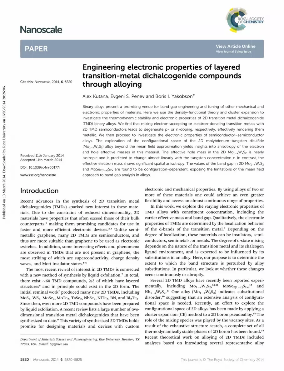
In order to select viable candidates for binary alloys, weconsidered pairs of TMD compounds that matched a set of pre-dened conditions based on specic descriptors and rules. Thedescriptors and rules that were used in the selection reected therequirements of a good match in the lattice constant and metal–chalcogen bond distance, as well as the band gap constraints.Mixtures of two metallic TMDs were not expected to display anite band gap, and were excluded by the rules. During the alloyselection, the following rules were imposed:
|a1 � a2|/max{a1,a2} < 0.034,
DdM�X < 0.1 A,
(Eg1 > 0)n(Eg2 > 0). (3)
Here, a1 and a2 are the lattice constants of the two TMDmaterials, Eg1 and Eg2 are their band gaps, and DdM�X is thedifference in the metal–chalcogen bond distance. The rst andsecond rules reect the requirements that the mismatch of thelattice constants between the two materials be smaller than 3%,and the difference in the metal–chalcogen bond distance be lessthan 0.1 A, respectively, whereas the third rule requires that atleast one of the compounds be a semiconductor.
Fig. 1 shows pairs of compounds that were selected based onthese rules, plotted according to their differences in theoreticalband gaps and mismatch of the lattice constants. The datapoints in the upper le corner of Fig. 1 correspond to the largestdifference in band gaps, as well as the smallest latticemismatch, potentially indicating the most favorable pairs. Theupper le corner of the plot is populated with vanadium–
molybdenum and vanadium–tungsten dichalcogenides. Thesematerials represent alloys between a metal (VX2) and a semi-conductor (MoX2, WX2).
We found that these types of metal-semiconductor alloys aredegenerate semiconductors at all mixings attained in calcula-tions. The doping mechanism was determined to be p-type,
Nanoscale, 2014, 6, 5820–5825 | 5821
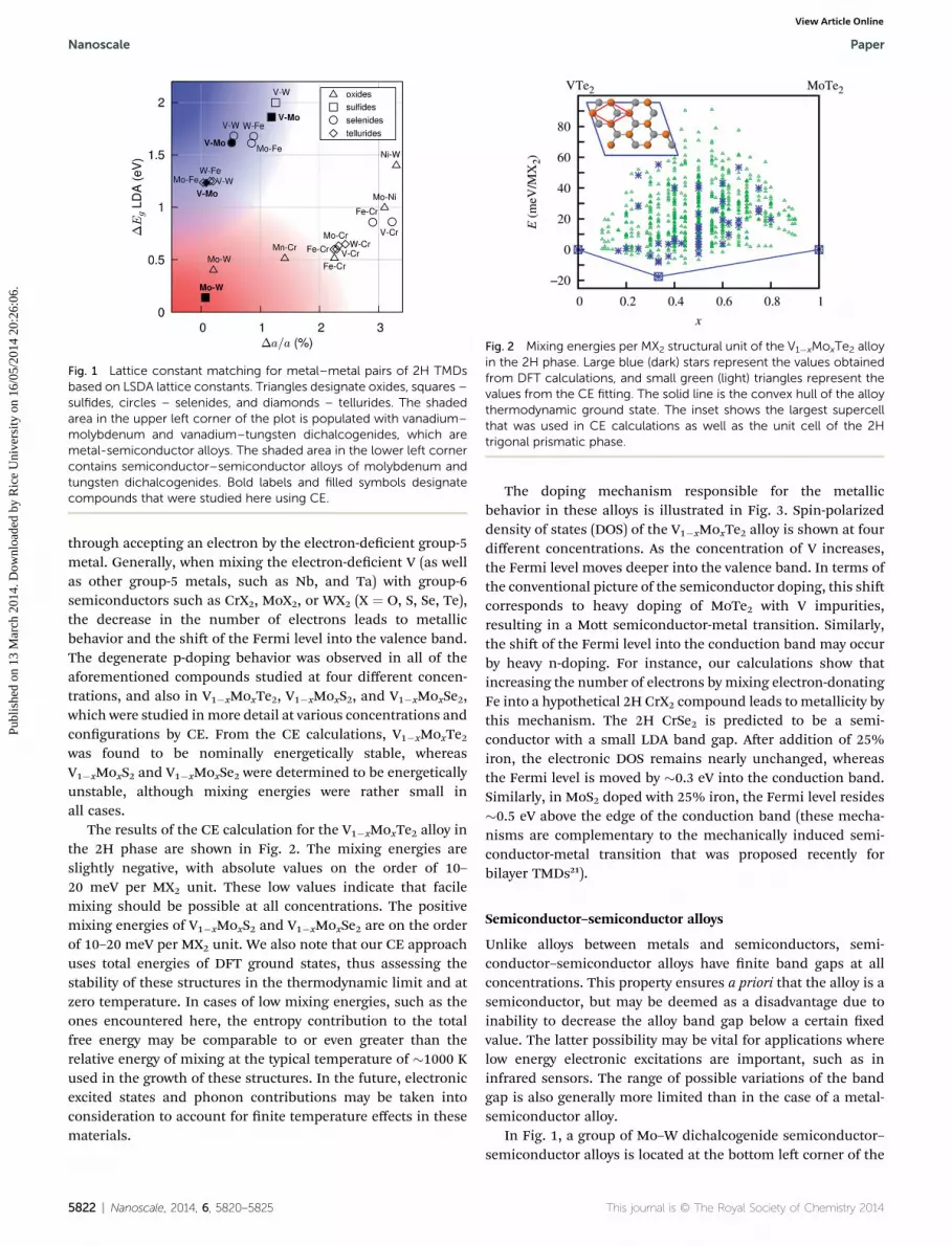
Fig. 1 Lattice constant matching for metal–metal pairs of 2H TMDsbased on LSDA lattice constants. Triangles designate oxides, squares –sulfides, circles – selenides, and diamonds – tellurides. The shadedarea in the upper left corner of the plot is populated with vanadium–molybdenum and vanadium–tungsten dichalcogenides, which aremetal-semiconductor alloys. The shaded area in the lower left cornercontains semiconductor–semiconductor alloys of molybdenum andtungsten dichalcogenides. Bold labels and filled symbols designatecompounds that were studied here using CE.
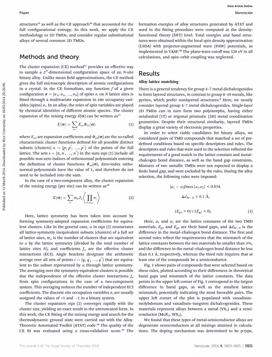
Fig. 2 Mixing energies per MX2 structural unit of the V1�xMoxTe2 alloyin the 2H phase. Large blue (dark) stars represent the values obtainedfrom DFT calculations, and small green (light) triangles represent thevalues from the CE fitting. The solid line is the convex hull of the alloythermodynamic ground state. The inset shows the largest supercellthat was used in CE calculations as well as the unit cell of the 2Htrigonal prismatic phase.
Nanoscale Paper
Publ
ishe
d on
13
Mar
ch 2
014.
Dow
nloa
ded
by R
ice
Uni
vers
ity o
n 16
/05/
2014
20:
26:0
6.
View Article Online
through accepting an electron by the electron-decient group-5metal. Generally, when mixing the electron-decient V (as wellas other group-5 metals, such as Nb, and Ta) with group-6semiconductors such as CrX2, MoX2, or WX2 (X ¼ O, S, Se, Te),the decrease in the number of electrons leads to metallicbehavior and the shi of the Fermi level into the valence band.The degenerate p-doping behavior was observed in all of theaforementioned compounds studied at four different concen-trations, and also in V1�xMoxTe2, V1�xMoxS2, and V1�xMoxSe2,which were studied inmore detail at various concentrations andcongurations by CE. From the CE calculations, V1�xMoxTe2was found to be nominally energetically stable, whereasV1�xMoxS2 and V1�xMoxSe2 were determined to be energeticallyunstable, although mixing energies were rather small inall cases.
The results of the CE calculation for the V1�xMoxTe2 alloy inthe 2H phase are shown in Fig. 2. The mixing energies areslightly negative, with absolute values on the order of 10–20 meV per MX2 unit. These low values indicate that facilemixing should be possible at all concentrations. The positivemixing energies of V1�xMoxS2 and V1�xMoxSe2 are on the orderof 10–20 meV per MX2 unit. We also note that our CE approachuses total energies of DFT ground states, thus assessing thestability of these structures in the thermodynamic limit and atzero temperature. In cases of low mixing energies, such as theones encountered here, the entropy contribution to the totalfree energy may be comparable to or even greater than therelative energy of mixing at the typical temperature of �1000 Kused in the growth of these structures. In the future, electronicexcited states and phonon contributions may be taken intoconsideration to account for nite temperature effects in thesematerials.
5822 | Nanoscale, 2014, 6, 5820–5825
The doping mechanism responsible for the metallicbehavior in these alloys is illustrated in Fig. 3. Spin-polarizeddensity of states (DOS) of the V1�xMoxTe2 alloy is shown at fourdifferent concentrations. As the concentration of V increases,the Fermi level moves deeper into the valence band. In terms ofthe conventional picture of the semiconductor doping, this shicorresponds to heavy doping of MoTe2 with V impurities,resulting in a Mott semiconductor-metal transition. Similarly,the shi of the Fermi level into the conduction band may occurby heavy n-doping. For instance, our calculations show thatincreasing the number of electrons by mixing electron-donatingFe into a hypothetical 2H CrX2 compound leads to metallicity bythis mechanism. The 2H CrSe2 is predicted to be a semi-conductor with a small LDA band gap. Aer addition of 25%iron, the electronic DOS remains nearly unchanged, whereasthe Fermi level is moved by �0.3 eV into the conduction band.Similarly, in MoS2 doped with 25% iron, the Fermi level resides�0.5 eV above the edge of the conduction band (these mecha-nisms are complementary to the mechanically induced semi-conductor-metal transition that was proposed recently forbilayer TMDs21).
Semiconductor–semiconductor alloys
Unlike alloys between metals and semiconductors, semi-conductor–semiconductor alloys have nite band gaps at allconcentrations. This property ensures a priori that the alloy is asemiconductor, but may be deemed as a disadvantage due toinability to decrease the alloy band gap below a certain xedvalue. The latter possibility may be vital for applications wherelow energy electronic excitations are important, such as ininfrared sensors. The range of possible variations of the bandgap is also generally more limited than in the case of a metal-semiconductor alloy.
In Fig. 1, a group of Mo–W dichalcogenide semiconductor–semiconductor alloys is located at the bottom le corner of the
This journal is © The Royal Society of Chemistry 2014
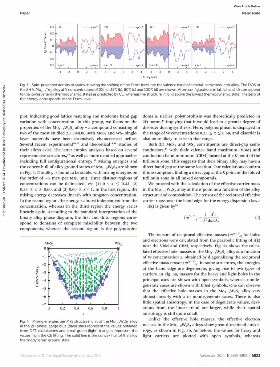
Fig. 3 Spin-projected density of states showing the shifting of the Fermi level into the valence band of a metal-semiconductor alloy. The DOS ofthe 2H VxMo1�xTe2 alloy at V concentrations of 0% (a), 33% (b), 80% (c) and 100% (d) are shown. Atom configurations in (a), (c), and (d) correspondto the lowest energy thermodynamic states as predicted by CE, whereas the structure in (b) is above the lowest thermodynamic state. The zero ofthe energy corresponds to the Fermi level.
Paper Nanoscale
Publ
ishe
d on
13
Mar
ch 2
014.
Dow
nloa
ded
by R
ice
Uni
vers
ity o
n 16
/05/
2014
20:
26:0
6.
View Article Online
plot, indicating good lattice matching and moderate band gapvariation with concentration. In this group, we focus on theproperties of the Mo1�xWxS2 alloy – a compound consisting oftwo of the most studied 2D TMDs. Both MoS2 and WS2 single-layer materials have been extensively characterized before.Several recent experimental10,22 and theoretical15,16 studies oftheir alloys exist. The latter employ analyses based on severalrepresentative structures,15 as well as more detailed approachesincluding full congurational entropy.16 Mixing energies andthe convex hull of alloy ground states of Mo1�xWxS2 are shownin Fig. 4. The alloy is found to be stable, with mixing energies onthe order of �5 meV per MX2 unit. Three distinct regions ofconcentrations can be delineated, viz. (1) 0 < x ( 0.33, (2)0.33 ( x ( 0.60, and (3) 0.60 ( x < 1. In the rst region, themixing energy decreases linearly with tungsten concentration.In the second region, the energy is almost independent from theconcentration, whereas in the third region the energy varieslinearly again. According to the standard interpretation of thebinary alloy phase diagram, the rst and third regions corre-spond to domains of complete miscibility between the twocomponents, whereas the second region is the polymorphic
Fig. 4 Mixing energies per MX2 structural unit of the Mo1�xWxS2 alloyin the 2H phase. Large blue (dark) stars represent the values obtainedfrom DFT calculations and small green (light) triangles represent thevalues from the CE fitting. The solid line is the convex hull of the alloythermodynamic ground state.
This journal is © The Royal Society of Chemistry 2014
domain. Earlier, polymorphism was theoretically predicted in2D boron,14 implying that it would lead to a greater degree ofdisorder during synthesis. Here, polymorphism is displayed inthe range of W concentrations 0.33 ( x( 0.60, and disorder isalso more likely to exist in that range.
Both 2D MoS2 and WS2 constituents are direct-gap semi-conductors,23 with their valence band maximum (VBM) andconduction band minimum (CBM) located at the K point of theBrillouin zone. This suggests that their binary alloy may have adirect band gap at the same location. Our calculations conrmthis assumption, nding a direct gap at the K point of the foldedBrillouin zone in all mixed compounds.
We proceed with the calculation of the effective carrier massin the Mo1�xWxS2 alloy at the K point as a function of the alloystructure and composition. The tensor of the reciprocal effectivecarrier mass near the band edge for the energy dispersion law 3
¼ 3(k) is given by24
�m*�1
�ij¼ 1
ħ2d23
dkidkj(4)
The tensors of reciprocal effective masses (m*�1)ij for holesand electrons were calculated from the parabolic tting of 3(k)near the VBM and CBM, respectively. Fig. 5a shows the calcu-lated effective hole masses in the Mo1�xWxS2 alloy as a functionof W concentration x, obtained by diagonalizing the reciprocaleffective mass tensor (m*�1)ij. In some structures, the energiesat the band edge are degenerate, giving rise to two types ofcarriers. In Fig. 5a, masses for the heavy and light holes in theprincipal axes are shown with open symbols, whereas nonde-generate cases are shown with lled symbols. One can observethat the effective hole masses in the Mo1�xWxS2 alloy varyalmost linearly with x in nondegenerate cases. There is alsolittle spatial anisotropy. In the case of degenerate values, devi-ations from the linear trend are larger, while their spatialanisotropy is still quite small.
Unlike the effective hole masses, the effective electronmasses in the Mo1�xWxS2 alloys show great directional anisot-ropy, as shown in Fig. 5b. As before, the values for heavy andlight carriers are plotted with open symbols, whereas
Nanoscale, 2014, 6, 5820–5825 | 5823
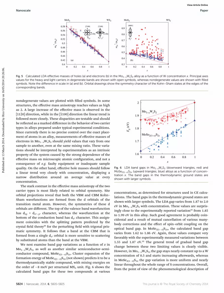
Fig. 5 Calculated LDA effective masses of holes (a) and electrons (b) in the Mo1�xWxS2 alloy as a function of W concentration x. Principal axesvalues for the heavy and light carriers in degenerate bands are shown with open symbols, whereas nondegenerate values are shown with filledsymbols. Note the difference in scale in (a) and (b). Orbital drawings show the symmetry character of the Kohn–Sham states at the edges of thecorresponding bands.
Fig. 6 LDA band gaps in Mo1�xWxS2 (downward triangles, red) andMoSe2(1�x)S2x (upward triangles, blue) alloys as a function of concen-tration x. The band gaps in the thermodynamic ground states areshown with larger symbols.
Nanoscale Paper
Publ
ishe
d on
13
Mar
ch 2
014.
Dow
nloa
ded
by R
ice
Uni
vers
ity o
n 16
/05/
2014
20:
26:0
6.
View Article Online
nondegenerate values are plotted with lled symbols. In somestructures, the effective mass anisotropy reaches values as highas 2. A large increase of the effective mass is observed in the[11�20] direction, while in the [�1100] direction the linear trend isfollowed more closely. These disparities are testable and shouldbe reected as amarked difference in the behavior of two carriertypes in alloys prepared under typical experimental conditions.Since currently there is no precise control over the exact place-ment of atoms in an alloy, measurements of effective masses ofelectrons in Mo1�xWxS2 should yield values that vary from onesample to another, even at the same mixing ratio. These varia-tions should be interpreted by experimentalists as an intrinsicproperty of the system caused by the strong dependence of theeffective mass on microscopic atomic conguration, and not aconsequence of e.g. faulty equipment or inadequate samplequality. On the other hand, effective hole masses should followa linear trend very closely with concentration, displaying anarrow distribution around an average value at everyconcentration.
The stark contrast in the effective mass anisotropy of the twocarrier types is most likely related to orbital symmetry. Siteorbital projections reveal that both the VBM and CBM Kohn–Sham wavefunctions are formed from the d orbitals of thetransition metal atom. However, the symmetries of these dorbitals are different. The top of the valence band wavefunctionhas dxy + dx2�y2 character, whereas the wavefunction at thebottom of the conduction band has dz2 character. This assign-ment coincides with the splitting pattern predicted by thecrystal eld theory25 for the perturbing eld with trigonal pris-matic symmetry. It follows that a band at the CBM that isformed from a single dz2 orbital is more sensitive to scatteringby substituted atoms than the band at the VBM.
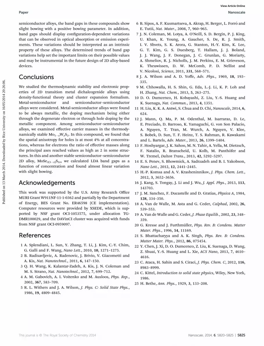
We next examine band gap variations as a function of x inMo1�xWxS2, as well as another similar semiconductor–semi-conductor compound, MoSe2(1�x)S2x. Cluster expansion of theformation energy of MoSe2(1�x)S2x (not shown) predicts it to be athermodynamically stable compound, with mixing energies onthe order of �8 meV per structural MX2 unit. Fig. 6 shows thecalculated band gaps for these two compounds at various
5824 | Nanoscale, 2014, 6, 5820–5825
concentrations, as determined for structures used in CE calcu-lations. The band gaps in the thermodynamic ground states areshown with larger symbols. The LDA gap varies from 1.87 to 2.0eV in Mo1�xWxS2 with concentration. These values are surpris-ingly close to the experimentally reported variation11 from 1.85to 1.99 eV in this alloy. Such good agreement is probably coin-cidental and a result of mutual cancellation of various many-body corrections and the effect of spin–orbit coupling on theoptical band gap. In MoSe2(1�x)S2x, the calculated band gapvaries from 1.62 to 1.86 eV. Again, these values compare veryfavorably with the experimentally measured variations between1.55 and 1.87 eV.12 The general trend of gradual band gapchange between these two limiting values is clearly visible.However, in Mo1�xWxS2, the gap stays nearly constant up to a Wconcentration of 0.5 and starts increasing aerwards, whereasin MoSe2(1�x)S2x the gap variation is more uniform and nearlylinear throughout the whole range of S concentrations. Overall,from the point of view of the phenomenological description of
This journal is © The Royal Society of Chemistry 2014
Paper Nanoscale
Publ
ishe
d on
13
Mar
ch 2
014.
Dow
nloa
ded
by R
ice
Uni
vers
ity o
n 16
/05/
2014
20:
26:0
6.
View Article Online
semiconductor alloys, the band gaps in these compounds showslight bowing with a positive bowing parameter. In addition,band gaps should display conguration-dependent variationsthat can be observed in optical absorption or emission experi-ments. These variations should be interpreted as an intrinsicproperty of these alloys. The determined trends of band gapvariations help set the important limits on their possible valuesand may be instrumental in the future design of 2D alloy-baseddevices.
Conclusions
We studied the thermodynamic stability and electronic prop-erties of 2D transition metal dichalcogenide alloys usingdensity-functional theory and cluster expansion formalism.Metal-semiconductor and semiconductor–semiconductoralloys were considered. Metal-semiconductor alloys were foundto be always metallic, the doping mechanism being eitherthrough the degenerate electron or through hole doping by themetallic component. Among semiconductor–semiconductoralloys, we examined effective carrier masses in the thermody-namically stable Mo1�xWxS2. In this compound, we found thatthe spatial anisotropy for holes is at most 4% at all concentra-tions, whereas for electrons the ratio of effective masses alongthe principal axes reached values as high as 2 in some struc-tures. In this and another stable semiconductor–semiconductor2D alloy, MoSe2(1�x)S2x, we calculated LDA band gaps as afunction of concentration and found almost linear variationwith slight bowing.
Acknowledgements
This work was supported by the U.S. Army Research OfficeMURI GrantW911NF-11-1-0362 and partially by the Departmentof Energy, BES Grant No. ER46598 (CE implementation).Computer resources were provided by XSEDE, which is sup-ported by NSF grant OCI-1053575, under allocation TG-DMR100029, and the DAVinCI cluster was acquired with fundsfrom NSF grant OCI-0959097.
References
1 A. Splendiani, L. Sun, Y. Zhang, T. Li, J. Kim, C.-Y. Chim,G. Galli and F. Wang, Nano Lett., 2010, 10, 1271–1275.
2 B. Radisavljevic, A. Radenovic, J. Brivio, V. Giacometti andA. Kis, Nat. Nanotechnol., 2011, 6, 147–150.
3 Q. H. Wang, K. Kalantar-Zadeh, A. Kis, J. N. Coleman andM. S. Strano, Nat. Nanotechnol., 2012, 7, 699–712.
4 A. M. Gabovich, A. I. Voitenko and M. Ausloos, Phys. Rep.,2002, 367, 583–709.
5 R. L. Withers and J. A. Wilson, J. Phys. C: Solid State Phys.,1986, 19, 4809–4845.
This journal is © The Royal Society of Chemistry 2014
6 B. Sipos, A. F. Kusmartseva, A. Akrap, H. Berger, L. Forro andE. Tutis, Nat. Mater., 2008, 7, 960–965.
7 J. N. Coleman, M. Lotya, A. O'Neill, S. D. Bergin, P. J. King,U. Khan, K. Young, A. Gaucher, S. De, R. J. Smith,I. V. Shvets, S. K. Arora, G. Stanton, H.-Y. Kim, K. Lee,G. T. Kim, G. S. Duesberg, T. Hallam, J. J. Boland,J. J. Wang, J. F. Donegan, J. C. Grunlan, G. Moriarty,A. Shmeliov, R. J. Nicholls, J. M. Perkins, E. M. Grieveson,K. Theuwissen, D. W. McComb, P. D. Nellist andV. Nicolosi, Science, 2011, 331, 568–571.
8 J. A. Wilson and A. D. Yoffe, Adv. Phys., 1969, 18, 193–335.
9 M. Chhowalla, H. S. Shin, G. Eda, L.-J. Li, K. P. Loh andH. Zhang, Nat. Chem., 2013, 5, 263–275.
10 D. O. Dumcenco, H. Kobayashi, Z. Liu, Y.-S. Huang andK. Suenaga, Nat. Commun., 2013, 4, 1351.
11 H. Liu, K. K. A. Antwi, S. Chua and D. Chi, Nanoscale, 2014, 6,624.
12 J. Mann, Q. Ma, P. M. Odenthal, M. Isarraraz, D. Le,E. Preciado, D. Barroso, K. Yamaguchi, G. von Son Palacio,A. Nguyen, T. Tran, M. Wurch, A. Nguyen, V. Klee,S. Bobek, D. Sun, T. F. Heinz, T. S. Rahman, R. Kawakamiand L. Bartels, Adv. Mater., 2013, 26, 1399–1404.
13 F. Hoshyargar, J. K. Sahoo, M. N. Tahir, A. Yella, M. Dietzsch,F. Natalio, R. Branscheid, U. Kolb, M. Panthofer andW. Tremel, Dalton Trans., 2013, 42, 5292–5297.
14 E. S. Penev, S. Bhowmick, A. Sadrzadeh and B. I. Yakobson,Nano Lett., 2012, 12, 2441–2445.
15 H.-P. Komsa and A. V. Krasheninnikov, J. Phys. Chem. Lett.,2012, 3, 3652–3656.
16 J. Kang, S. Tongay, J. Li and J. Wu, J. Appl. Phys., 2013, 113,143703.
17 J. M. Sanchez, F. Ducastelle and D. Gratias, Physica A, 1984,128, 334–350.
18 A. Van de Walle, M. Asta and G. Ceder, Calphad, 2002, 26,539–553.
19 A. Van deWalle and G. Ceder, J. Phase Equilib., 2002, 23, 348–359.
20 G. Kresse and J. Furthmuller, Phys. Rev. B: Condens. MatterMater. Phys., 1996, 54, 11169.
21 S. Bhattacharyya and A. K. Singh, Phys. Rev. B: Condens.Matter Mater. Phys., 2012, 86, 075454.
22 Y. Chen, J. Xi, D. O. Dumcenco, Z. Liu, K. Suenaga, D. Wang,Z. Shuai, Y.-S. Huang and L. Xie, ACS Nano, 2013, 7, 4610–4616.
23 C. Ataca, H. Sahin and S. Ciraci, J. Phys. Chem. C, 2012, 116,8983–8999.
24 C. Kittel, Introduction to solid state physics, Wiley, New York,1986.
25 H. Bethe, Ann. Phys., 1929, 3, 133–208.
Nanoscale, 2014, 6, 5820–5825 | 5825
Related Documents


![Li Alloying Nanomaterials - greenlionproject.eu · where M represents a group IV alloying element.[5] This equation implies a 3.75:1 lithium to alloying element atomic ratio at full](https://static.cupdf.com/doc/110x72/5f7894293cf36b12a9415e0d/li-alloying-nanomaterials-where-m-represents-a-group-iv-alloying-element5-this.jpg)


