1 Prepared by L.M.I.Leo Joseph A.P/ECE MAHALAKSHMI ENGINEERING COLLEGE TIRUCHIRAPALLI – 621213 QUESTION BANK DEPARTMENT: ECE SEMESTER – III SUBJECT NAME: DIGITAL SYSTEM DESIGN SUBJECT CODE: EC2203 UNIT 2 : Design of Combinational Circuits PART -A (2 Marks) 1. Design a half subtractor. (AUC MAY 2013)

Welcome message from author
This document is posted to help you gain knowledge. Please leave a comment to let me know what you think about it! Share it to your friends and learn new things together.
Transcript
1 Prepared by L.M.I.Leo Joseph A.P/ECE
MAHALAKSHMI
ENGINEERING COLLEGE
TIRUCHIRAPALLI – 621213
QUESTION BANK
DEPARTMENT: ECE SEMESTER – III
SUBJECT NAME: DIGITAL SYSTEM DESIGN SUBJECT CODE: EC2203
UNIT 2 : Design of Combinational Circuits
PART -A (2 Marks)
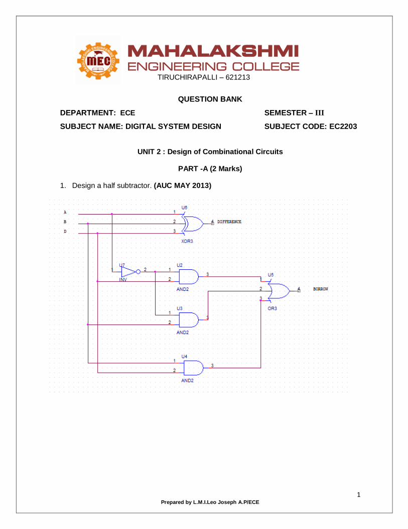
1. Design a half subtractor. (AUC MAY 2013)

2 Prepared by L.M.I.Leo Joseph A.P/ECE
2. Write down the truth table of full subtractor. (AUC MAY 2012 , 2013)
3. What is meant by look ahead carry
? (AUC NOV 2011,NOV 2008)
In parallel addition time delay occurs,the process of overcoming this time delay is called look ahead carry.
4. Give the logical expression for sum output and carry output of a full adder.
(AUC NOV 2011)
Sum = A + B + C Carry =AB+AC+BC 5. Design a single bit magnitude comparator to compare two words A and B. (AUC
APR 2011)
6. Write an expression for borrow and difference in a full subtractor circuit.
A B D DIFFERENCE BORROW
0 0 0 0 0
0 0 1 1 1
0 1 0 1 1
0 1 1 0 1
1 0 0 1 0
1 0 1 0 0
1 1 0 0 0
1 1 1 1 1
A B A=B A>B A<B
0 0 1 0 0
0 1 0 0 1
1 0 0 1 0
1 1 1 0 0

3 Prepared by L.M.I.Leo Joseph A.P/ECE
(AUC APR 2010)
Difference = A’B’D+A’BD’+AB’D’+ABD Borrow = A + B+ D 7. Draw the circuits diagram for 4 bit Odd parity generator. (AUC APR 2010, APR 2007)
8. Suggest a solution to overcome the limitation on the speed of an adder.
(AUC NOV 2009)
By eliminating the interstage carry delay we can increase the speed of addition. 9. Differentiate a decoder from a demultiplexer. (AUC NOV 2009)
DECODER DEMULTIPLEXER
A decoder is a multiple –input ,multiple-output logic circuit which converts coded input into coded outputs, where the input and output codes are different.
A demultiplexer is a circuit that receives information on a single line and transmit this information on one of the 2n possible output lines.
10. Define combinational logic .
When logic gates are connected together to produce a specified output for certain specified combinations of input variables, with no storage involved, the resulting circuit is called combinational logic.
11. Define Decoder?
A decoder is a multiple - input multiple output logic circuit that converts coded inputs into coded outputs where the input and output codes are different.
12. What is binary decoder?
A decoder is a combinational circuit that converts binary information from n input lines to a maximum of 2n out puts lines.
13. Define Encoder?
An encoder has 2n input lines and n output lines. In encoder the output lines generate the
U8
XOR2
1
23
B
U10
XOR2
1
23
C U9
XOR2
1
23
D
(A+B) XNOR (C+D)
A

4 Prepared by L.M.I.Leo Joseph A.P/ECE
binary code corresponding to the input value.
14. What is priority Encoder?
A priority encoder is an encoder circuit that includes the priority function. In priority encoder, if 2 or more inputs are equal to 1 at the same time, the input having the highest priority will take precedence.
15. Define multiplexer?
Multiplexer is a digital switch. If allows digital information from several sources to be routed onto a single output line.
16. What do you mean by comparator? A comparator is a special combinational circuit designed primarily to compare the relative magnitude of two binary numbers.
17. What is propagation delay?
Propagation delay is the average transition delay time for the signal to propogate form input to output when the signals changes its value. It is expressed in ms.
Part –B (16 Marks)
1. Design a full adder using two half adders. (AUC MAY 2013)
Full adder takes a three-bits input. Adding two single-bit binary values X, Y with a carry input bit C-in produces a sum bit S and a carry out C-out bit.
Truth Table
A B CIN SUM CARRY
0 0 0 0 0
0 0 1 1 0
0 1 0 1 0
0 1 1 0 1
1 0 0 1 0
1 0 1 0 1
1 1 0 0 1
1 1 1 1 1
SUM (X, Y, Z) = (1, 2, 4, 7) CARRY (X, Y, Z) = (3, 5, 6, 7)
Kmap-SUM

5 Prepared by L.M.I.Leo Joseph A.P/ECE
SUM = X'Y'Z + XY'Z' + X'YZ'
SUM = X Y Z
Kmap -CARRY
CARRY = XY + XZ + YZ Logic diagram:
Full adder circuit using half adders:
SUM= A xor B xor CIN CARRY = AB+BC+CA
C
U1A
7486
1
23
U4A
7408
1
23
B
U2A
7408
1
23
carryU5A
7432
1
23
A
sumU3A
7486
1
23

6 Prepared by L.M.I.Leo Joseph A.P/ECE
2. Design a 4 bit magnitude comparator and draw the circuit. (AUC MAY 2013)
A magnitude comparator is a combinational circuit that compares the magnitude of two numbers (A and B) and generates one of the following outputs: A=B, A>B, A<B.
Let A3 EXNOR B3 =x3 A2 EXNOR B2 =x2 A1 EXNOR B1 =x1 A0 EXNOR B0 =x0 From the table A>B = A3B3’+X3 A2B2’+X3X2A1B1’+X3X2X1A0B0’ A<B =A3’B3+X3A2’B2+X3X2A1’B1+X3X2X1A0’B0 A=B = X3X2X1X0 LOGIC DIAGRAM
GROUP A3 A2 A1 A0 B3 B2 B1 Bo Condition
I 1 x x x 0 x x x A>B
0 x x x 1 x x x A<B
II 1 1 x x 1 0 x X A>B
1 0 x x 1 1 x X A<B
0 1 x x 0 0 x X A>B
0 0 x x 0 1 x x A<B
III 1 1 1 x 1 1 0 x A>B
1 1 0 x 1 1 1 X A<B
0 0 1 x 0 0 0 X A>B
0 0 0 X 0 0 1 X A<B
IV 1 1 1 1 1 1 1 0 A>B
1 1 1 0 1 1 1 1 A<B
0 0 0 1 0 0 0 0 A>B
0 0 0 0 0 0 0 1 A<B
V 1 1 1 1 0 0 0 0 A=B
0 0 0 0 1 1 1 1 A=B

7 Prepared by L.M.I.Leo Joseph A.P/ECE
3. Design a combinational circuit to convert binary to gray code. (AUC MAY 2013,2009)
BLOCK DIAGRAM
K-Map for G3:
G3 = B3
4 bit binary input
4 bit binary gray
o/p
biary to gray code converter

8 Prepared by L.M.I.Leo Joseph A.P/ECE
K-Map for G2:
K-Map for G1:
K-Map for G0:

9 Prepared by L.M.I.Leo Joseph A.P/ECE
TRUTH TABLE: | Binary input | Gray code output
B3 B2 B1 B0 G3 G2 G1 G0
0 0 0 0 0 0 0 0 1 1 1 1 1 1 1 1
0 0 0 0 1 1 1 1 0 0 0 0 1 1 1 1
0 0 1 1 0 0 1 1 0 0 1 1 0 0 1 1
0 1 0 1 0 1 0 1 0 1 0 1 0 1 0 1
0 0 0 0 0 0 0 0 1 1 1 1 1 1 1 1
0 0 0 0 1 1 1 1 1 1 1 1 0 0 0 0
0 0 1 1 1 1 0 0 0 0 1 1 1 1 0 0
0 1 1 0 0 1 1 0 0 1 1 0 0 1 1 0
4. Design Half and Full subtractor circuits (AUC MAY 2012)
SUBTRACTOR Half subtractor The half-subtractor is a combinational circuit which is used to perform subtraction
of two bits. It has two inputs, X (minuend) and Y (subtrahend) and two outputs D (difference) and B (borrow).
X Y D B
0 0 0 0
0 1 1 1
1 0 1 0
1 1 0 0

10 Prepared by L.M.I.Leo Joseph A.P/ECE
The Full_subtractor is a combinational circuit which is used to perform subtraction of three bits. It has three inputs, X (minuend) and Y (subtrahend) and Z (subtrahend) and two outputs D (difference) and B (borrow).
X Y Z D B
0 0 0 0 0
0 0 1 1 1
0 1 0 1 1
0 1 1 0 1
1 0 0 1 0
1 0 1 0 0
1 1 0 0 0
1 1 1 1 1
B=A‟B + A‟C + BC C=A xor B xor C

11 Prepared by L.M.I.Leo Joseph A.P/ECE
5. a)Draw the circuit of BCD adder and explain. (AUC NOV 2011,2013)
BCD addition is the same as binary addition with a bit of variation: whenever a sum is greater than 1001, it is not a valid BCD number, so we add 0110 to it, to do the correction. This will produce a carry, which is added to the next BCD position. Add the two 4-bit BCD code inputs.
if the sum of this addition is greater than 1001; if yes, then add 0110 to this sum and generate a carry to the next decimal position.
LOGIC DIAGRAM:
K MAP

12 Prepared by L.M.I.Leo Joseph A.P/ECE
Y = S4 (S3 + S2) TRUTH TABLE:
BCD SUM CARRY
S4 S3 S2 S1 C
0 0 0 0 0
0 0 0 1 0
0 0 1 0 0
0 0 1 1 0
0 1 0 0 0
0 1 0 1 0
0 1 1 0 0
0 1 1 1 0
1 0 0 0 0
1 0 0 1 0
1 0 1 0 1
1 0 1 1 1
1 1 0 0 1
1 1 0 1 1
1 1 1 0 1
1 1 1 1 1
b) What is priority encoder? How is it different from encoder? Draw the circuit of 4
bit priority encoder and explain. (AUC NOV 2011) If more than two inputs are active simultaneously, the output is unpredictable or rather it is not what we expect it to be. This ambiguity is resolved if priority is established so that only one input is encoded, no matter how many inputs are active at a given point of time. The priority encoder includes a priority function. The operation of the priority encoder is such that if two or more inputs are active at the same time, the input having the highest priority will take precedence.
Example - 4to3 Priority Encoder
The truth table of a 4-input priority encoder is as shown below. The input D3 has the highest priority, D2 has next highest priority, and D0 has the lowest priority. This means output Y2 and Y1 are 0 only when none of the inputs D1, D2, D3 are high and only D0 is high. A 4 to 3 encoder consists of four inputs and three outputs, truth table and symbols of which is shown below.
Truth Table
D3 D2 D1 D0 Y2 Y1 Y0
0 0 0 0 0 0 0
0 0 0 1 0 0 1
0 0 1 x 0 1 0
0 1 x x 0 1 1
1 x x x 1 0 0

13 Prepared by L.M.I.Leo Joseph A.P/ECE
Kmaps
6. (i) Implement full subtractor using demultiplexer. (10) (AUC NOV 2009)
Full Subtracter
A full subtracter is a combinational circuit that performs subtraction involving three bits, namely minuend, subtrahend, and borrow-in. The logic symbol and truth table are shown below.
Truth Table
A B Bin difference Borrow
0 0 0 0 0
0 0 1 1 1
0 1 0 1 1
0 1 1 0 1
1 0 0 1 0
1 0 1 0 0
1 1 0 0 0
1 1 1 1 1
Difference = ∑m(1,2,4,7) Borrow = ∑m(1,2,3,7)
I0 I1 I2 I3
A’ 0 1 2 3
A 4 5 6 7
A A’ A’ A
I0 ,I3 ------- A I1 ,I2 ----------A’ (ii) Implement the given Boolean function using 8 : 1 multiplexer F(A, B, C) = Σ(1, 3, 5, 6) . (6) (AUC NOV 2009)
I0 -----------0 I1 ----------1 I2 ----------- A I3-------------A’
I0 I1 I2 I3
A’ 0 1 2 3
A 4 5 6 7
0 1 A A’
Related Documents