ENGG3190 Logic Synthesis “Sequential Circuit Synthesis” Winter 2014 S. Areibi School of Engineering University of Guelph

ENGG3190 Logic Synthesis “Sequential Circuit Synthesis” Winter 2014 S. Areibi School of Engineering University of Guelph.
Dec 14, 2015
Welcome message from author
This document is posted to help you gain knowledge. Please leave a comment to let me know what you think about it! Share it to your friends and learn new things together.
Transcript

ENGG3190Logic Synthesis
“Sequential Circuit Synthesis”
Winter 2014S. Areibi
School of EngineeringUniversity of Guelph
2
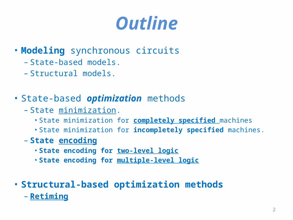
Outline• Modeling synchronous circuits
– State-based models.– Structural models.
• State-based optimization methods– State minimization.
• State minimization for completely specified machines• State minimization for incompletely specified machines.
– State encoding• State encoding for two-level logic• State encoding for multiple-level logic
• Structural-based optimization methods– Retiming
3
Combinational vs. Sequential Circuits
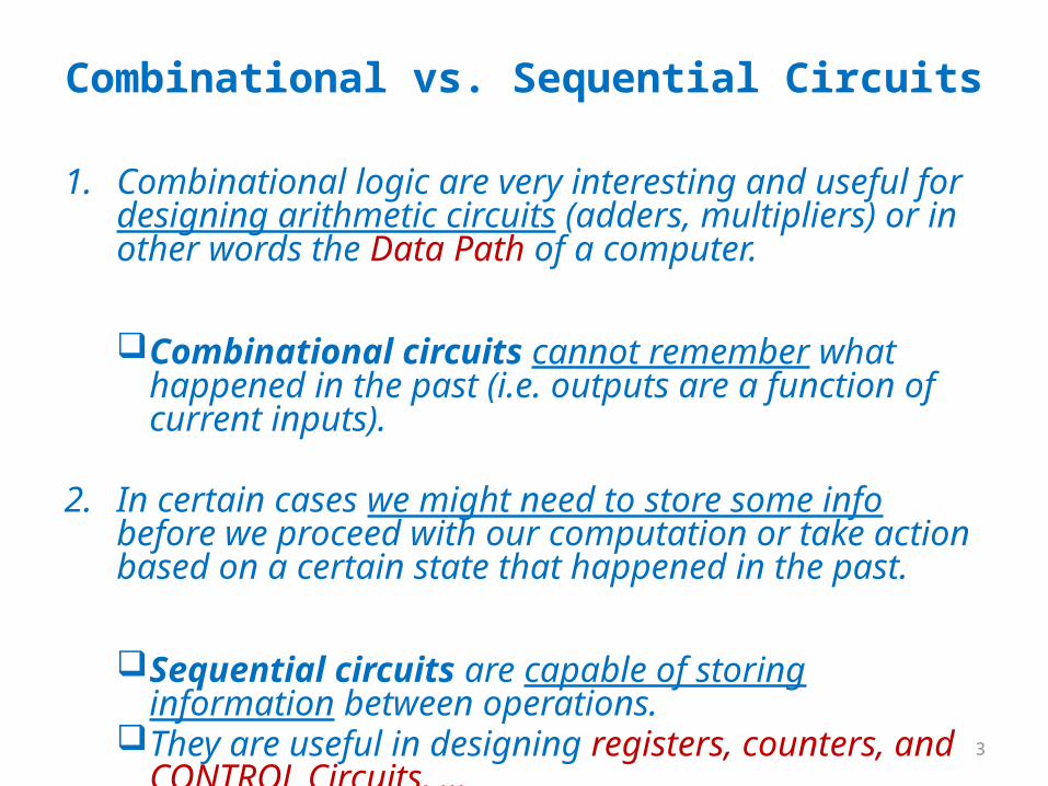
1. Combinational logic are very interesting and useful for designing arithmetic circuits (adders, multipliers) or in other words the Data Path of a computer.
Combinational circuits cannot remember what happened in the past (i.e. outputs are a function of current inputs).
2. In certain cases we might need to store some info before we proceed with our computation or take action based on a certain state that happened in the past.
Sequential circuits are capable of storing information between operations.
They are useful in designing registers, counters, and CONTROL Circuits, …

4
Types of Sequential Circuits
Two main types and their classification depends on the times at which their inputs are observed and their internal state changes.
Synchronous: State changes synchronized by one or more clocks
Asynchronous: Changes occur independently

What are Sequential Circuits?
Some sequential circuits have memory elements.– Synchronous circuits have clocked latches. – Asynchronous circuits may or may not have latches (e.g. C-elements),
but these are not clocked.
Feedback (cyclic) is a necessary, but not sufficient condition for a circuit to be sequential.
Synthesis of sequential circuits is not as well developed as combinational. (only small circuits)
Sequential synthesis techniques are not really used in commercial software (except maybe retiming).
Sequential verification is a problem.

6
Synchronous/Asynchronous
Analog
Asynchronous
Synchronous
Time
Continuous in value &
time
Discrete in value & continuous
in time
Discrete in value &
time
Digital

7
Comparison
Synchronous Easier to analyze because can factor out gate delays Speed of the system is determined by the clock (maybe slowed!)
Asynchronous Potentially faster Harder to analyze
We will only look at Synchronous Circuits

Example
The above circuit is sequential since primary output depends on the state and primary inputs.
LatchPresent State Next State
in1in2
in3
in4
out 1
prim
ary
inpu
ts
primary output
0
1
---1/1
----/1
(--00, 11-0)/0
(1010, 0110)/1
Registers and Latches (Netlist) State Transition Graph (STG)

9
Analysis of Sequential Circuits
The behavior of a sequential circuit is determined from: Inputs, Outputs, Present state of the circuit.
The analysis of a sequential circuit consists of: Obtaining a suitable description that
demonstrates the time sequence of inputs, outputs and states (STATE DIAGRAM).
10
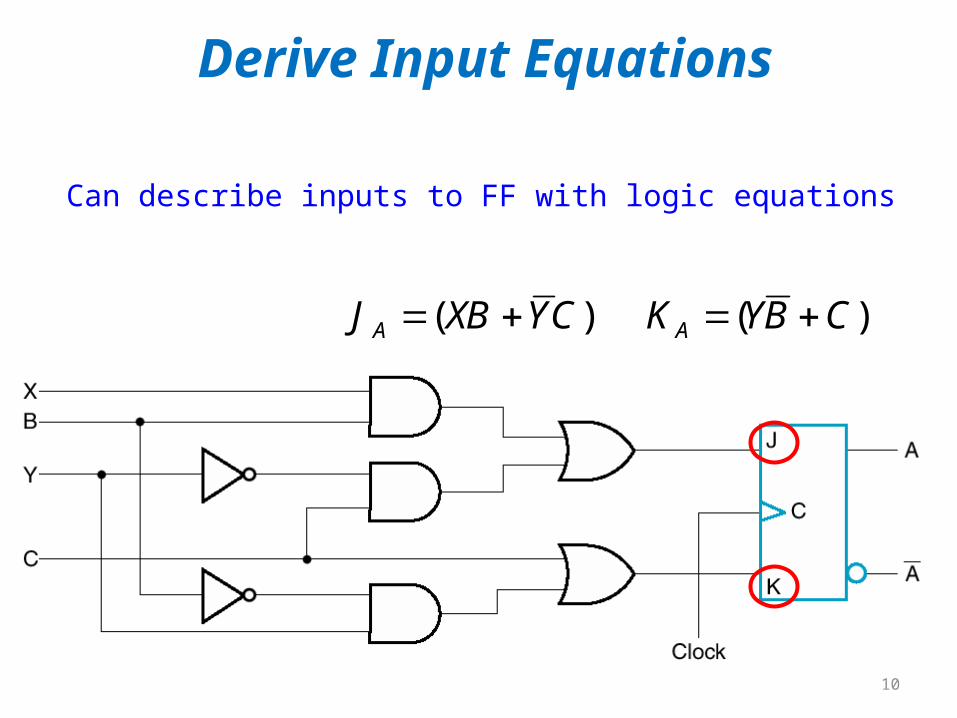
Derive Input Equations
Can describe inputs to FF with logic equations
)( CYXBJ A )( CBYK A

11
State Table Similar to truth table with state added A sequential circuit with `m’ FFs and `n’ inputs needs 2m+n rows
in state table.
)( BXAXDA XADB XBAY )(

12
State Diagram • An alternative
representation to State Table
Input/Output
InputOutput
“Mealy Model”

13
State Diagram: Moore
Alternative representation for state table
State/OutputInputs
14
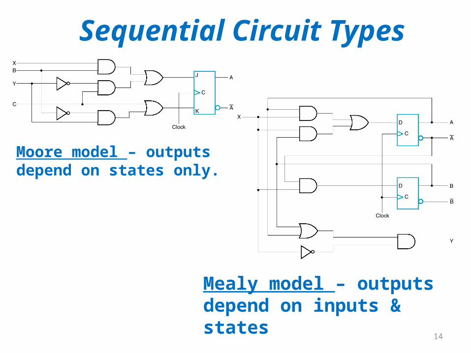
Sequential Circuit Types
Moore model – outputs depend on states only.
Mealy model – outputs depend on inputs & states

15
Moore vs. Mealy Machine
Moore Machine: Easy to understand and easy to code. Might requires more states (thus more hardware).
Mealy Machine: They are more general than Moore Machines More complex since outputs are a function of both the state and input. Requires less states in most cases, therefore less components.
Choice of a model depends on the application and personal preference.
You can transform a Mealy Machine to a Moore Machine and vice versa.
16
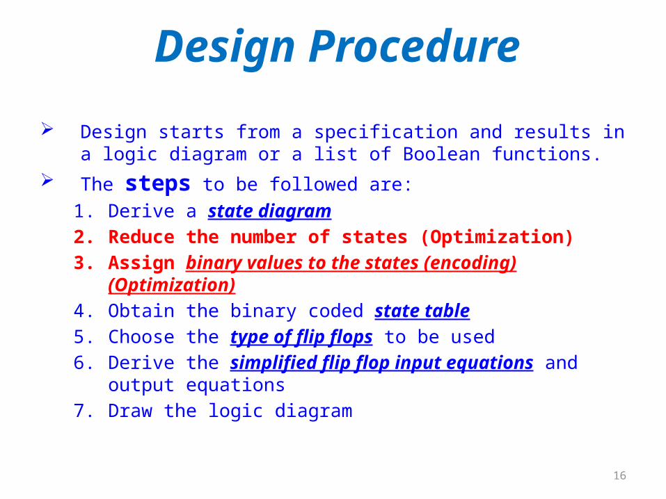
Design Procedure
Design starts from a specification and results in a logic diagram or a list of Boolean functions.
The steps to be followed are:1. Derive a state diagram2. Reduce the number of states (Optimization)3. Assign binary values to the states (encoding) (Optimization)4. Obtain the binary coded state table5. Choose the type of flip flops to be used6. Derive the simplified flip flop input equations and output equations7. Draw the logic diagram

17
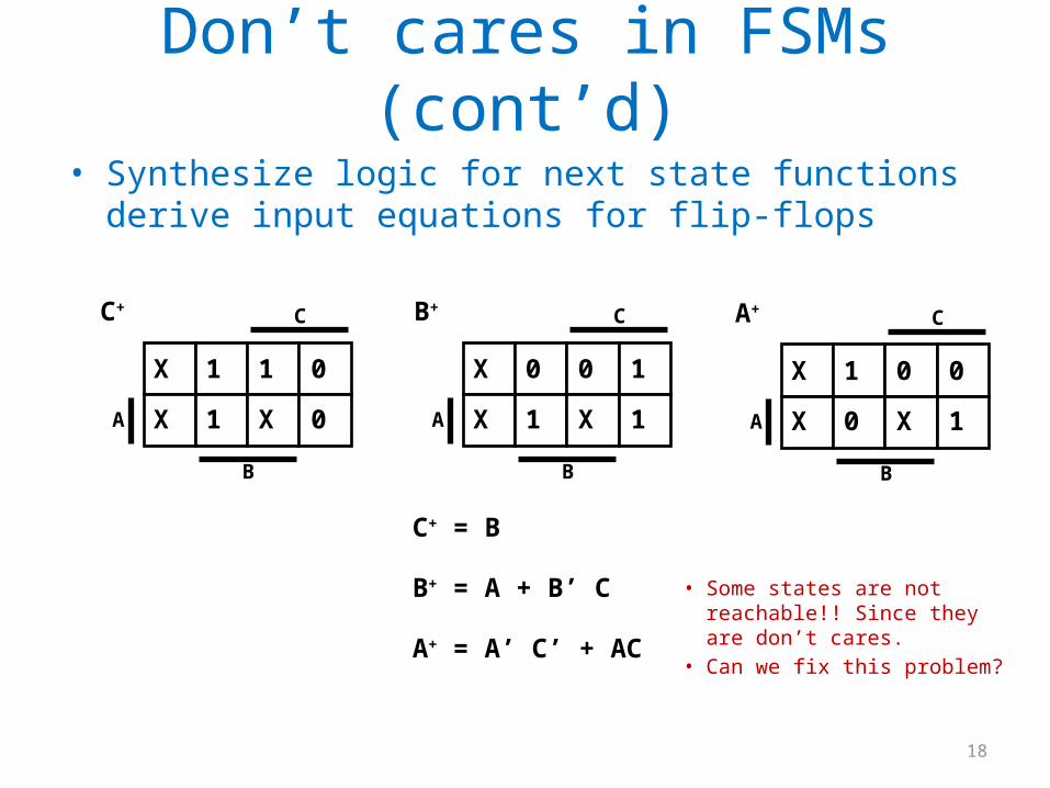
Present State Next StateC B A C+ B+ A+0 0 0 x x x0 0 1 x x x0 1 0 1 0 10 1 1 1 1 01 0 0 0 1 01 0 1 0 1 11 1 0 1 0 01 1 1 x x x
note the don't care conditions that arise from the unused state codes
Synthesis Example
• Implement simple count sequence: 000, 010, 011, 101, 110
• Derive the state transition table from the state transition diagram
101
010 100
110
011
18
C
B
A
X 1 1 0
X 1 X 0
C+ C
B
A
X 0 0 1
X 1 X 1
B+C
B
A
X 1 0 0
X 0 X 1
A+
C+ = B
B+ = A + B’ C
A+ = A’ C’ + AC
Don’t cares in FSMs (cont’d)• Synthesize logic for next state functions derive input
equations for flip-flops
• Some states are not reachable!! Since they are don’t cares.
• Can we fix this problem?
19
Self-starting FSMs• Deriving state transition table from don't care assignment
C
B
A
0 1 1 0
0 1 1 0
C+ C
B
A
1 0 0 1
1 1 1 1
B+C
B
A
1 1 0 0
0 0 1 1
A+
Present State Next StateC B A C+ B+ A+0 0 0 0 1 10 0 1 0 1 00 1 0 1 0 10 1 1 1 1 01 0 0 0 1 01 0 1 0 1 11 1 0 1 0 01 1 1 1 1 x
20
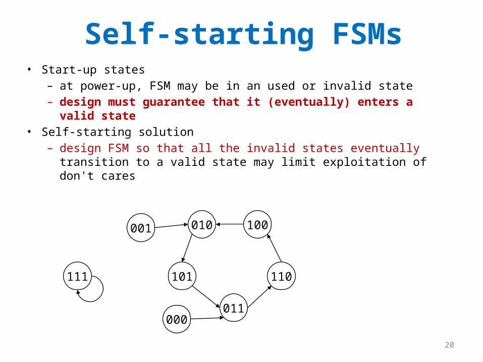
Self-starting FSMs• Start-up states
– at power-up, FSM may be in an used or invalid state– design must guarantee that it (eventually) enters a valid state
• Self-starting solution– design FSM so that all the invalid states eventually transition to a valid
state may limit exploitation of don't cares
101
010 100
110
011000
001
111
21
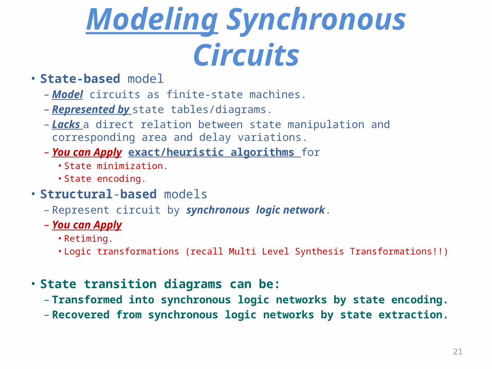
Modeling Synchronous Circuits• State-based model
– Model circuits as finite-state machines.– Represented by state tables/diagrams.– Lacks a direct relation between state manipulation and corresponding area and
delay variations.– You can Apply exact/heuristic algorithms for
• State minimization.• State encoding.
• Structural-based models– Represent circuit by synchronous logic network.– You can Apply
• Retiming.• Logic transformations (recall Multi Level Synthesis Transformations!!)
• State transition diagrams can be:– Transformed into synchronous logic networks by state encoding.– Recovered from synchronous logic networks by state extraction.

22
General Logic Structure
• Combinational optimization– keep latches/registers at current positions, keep their function– optimize combinational logic in between
• Sequential optimization– change latch position/function (retiming)
Combinational logic (CL)
Sequential elements

Overview of FSM Optimization
Specification
State Minimization
State Encoding
Logic/Timing Optimization
Verification/Testing

24
State-Based Models: Optimization
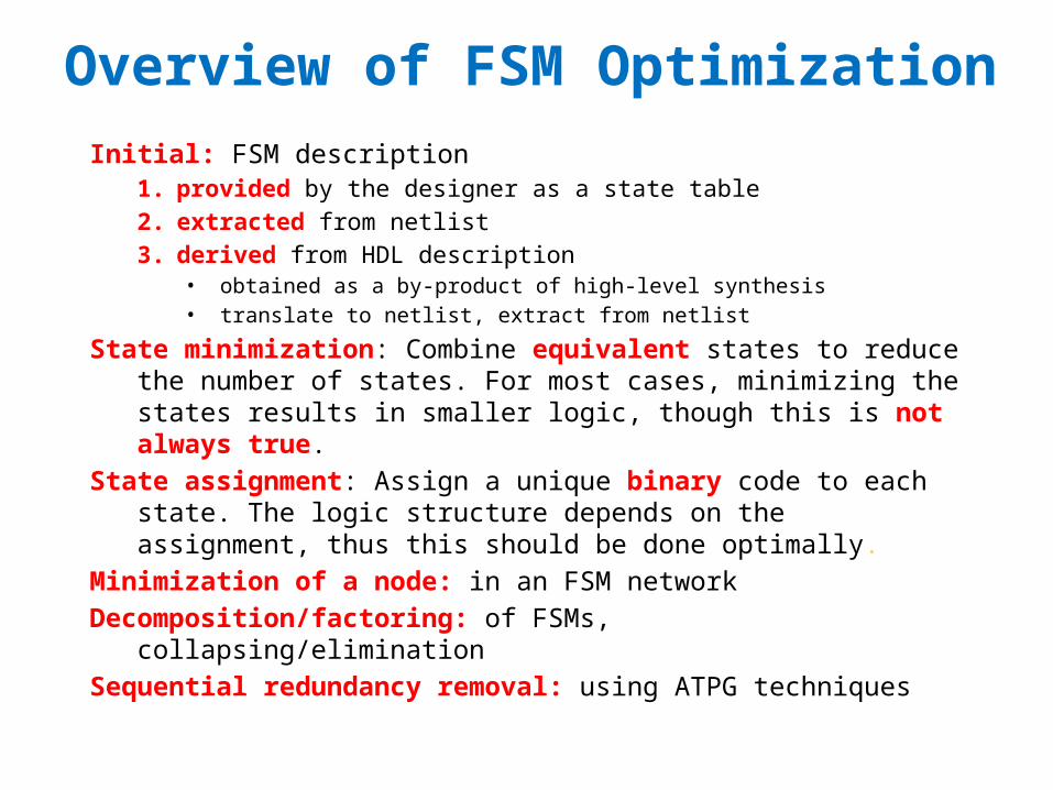
Overview of FSM OptimizationInitial: FSM description
1. provided by the designer as a state table2. extracted from netlist3. derived from HDL description
• obtained as a by-product of high-level synthesis• translate to netlist, extract from netlist
State minimization: Combine equivalent states to reduce the number of states. For most cases, minimizing the states results in smaller logic, though this is not always true.
State assignment: Assign a unique binary code to each state. The logic structure depends on the assignment, thus this should be done optimally.
Minimization of a node: in an FSM networkDecomposition/factoring: of FSMs, collapsing/eliminationSequential redundancy removal: using ATPG techniques
26
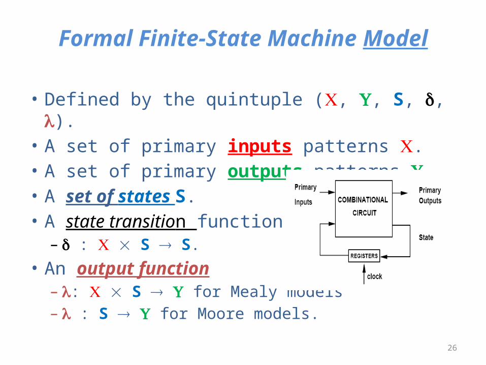
Formal Finite-State Machine Model
• Defined by the quintuple (, , S, , ).• A set of primary inputs patterns .• A set of primary outputs patterns .• A set of states S.• A state transition function
– : S S.• An output function
– : S for Mealy models– : S for Moore models.

27
State Minimization• Definition: Derive a FSM with similar behavior and minimum
number of states.– Aims at reducing the number of machine states – reduces the size of transition table.
• State reduction may reduce? – the number of storage elements.– the combinational logic due to reduction in transitions
• Types:1. Completely specified finite-state machines
• No don't care conditions.• Easy to solve.
2. Incompletely specified finite-state machines• Unspecified transitions and/or outputs.• Intractable problem.
28
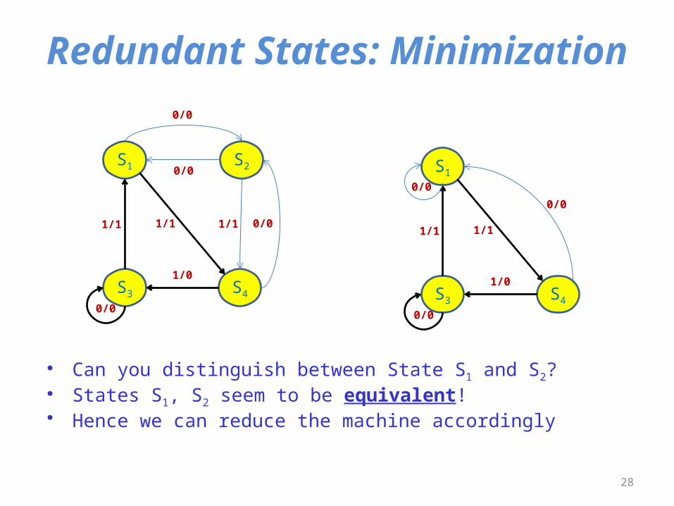
Redundant States: Minimization
S1
S4
S2
S3
1/1
1/0
0/01/1
0/0
0/0
1/1
0/0
• Can you distinguish between State S1 and S2?• States S1, S2 seem to be equivalent!• Hence we can reduce the machine accordingly
S1
S4S3
1/1
1/0
0/0
1/1
0/0
0/0

29
State Minimization for Completely-Specified FSMs
• Def: Equivalent states– Given any input sequence the corresponding
output sequences match.• Theorem: Two states are equivalent iff
I. they lead to identical outputs andII. their next-states are equivalent.
• Since equivalence is symmetric and transitive– States can be partitioned into equivalence classes.– Such a partition is unique.

Equivalent States• Two states of an FSM are:
– equivalent (or indistinguishable) – if for each input they produce the same output and their next
states are identical.
30
Si
Sj
Sm
Sn
1/0
1/0
0/0
0/0
Si,j
Sm
Sn
1/0
0/0
Si and Sj are equivalent andmerged into a single state.

Algorithmic State Minimization• Goal – identify and combine states that have
equivalent behavior– Reduced machine is smaller, faster, consumes less power.
• Algorithm Sketch1. Place all states in one set2. Initially partition set based on output behavior3. Successively partition resulting subsets based on next
state transitions4. Repeat (3) until no further partitioning is required
• states left in the same set are equivalentPolynomial time procedure

Equivalent States … Cont• Example: States A . . . I, Inputs I1, I2, Output, Z
32
Present state
Next state, output (Z)
InputI1 I2
A D / 0 C / 1
B E / 1 A / 1
C H / 1 D / 1
D D / 0 C / 1
E B / 0 G / 1
F H / 1 D /1
G A / 0 F / 1
H C / 0 A / 1
I G / 1 H / 1
A and D are equivalent
A and E produce same outputQ: Can they be equivalent?A: Yes, if B and D were equivalent and C and G were equivalent.

33
Minimization Algorithm
• Stepwise partition refinement.• Let i , i= 1, 2, …., n denote the partitions.• Initially
– 1 = States belong to the same block when outputs are the same for any input.
• Refine partition blocks: While further splitting is possible– k+1 = States belong to the same block if they were previously in the same
block and their next-states are in the same block of k for any input.
• At convergence i+1 = i
– Blocks identify equivalent states.

34
Example …• 1 = {(s1, s2), (s3, s4), (s5)}.
• Split s3, s4 • 2 = {(s1, s2), (s3), (s4), (s5)}.
• 2 = is a partition into equivalence classes– States (s1, s2) are
equivalent.
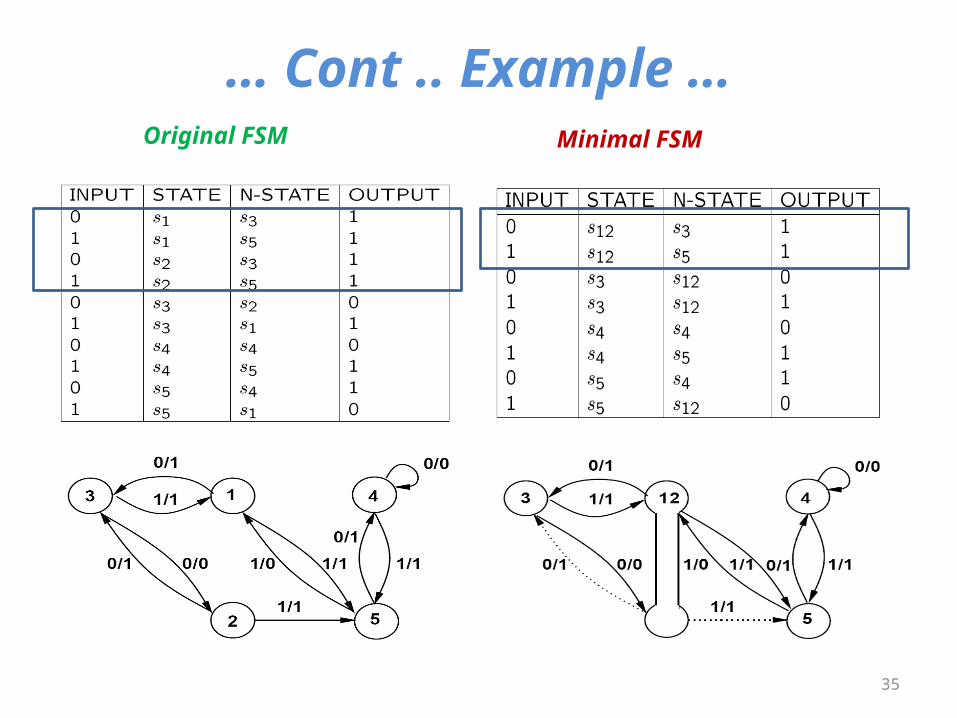
35
… Cont .. Example …Original FSM Minimal FSM
36
… Example
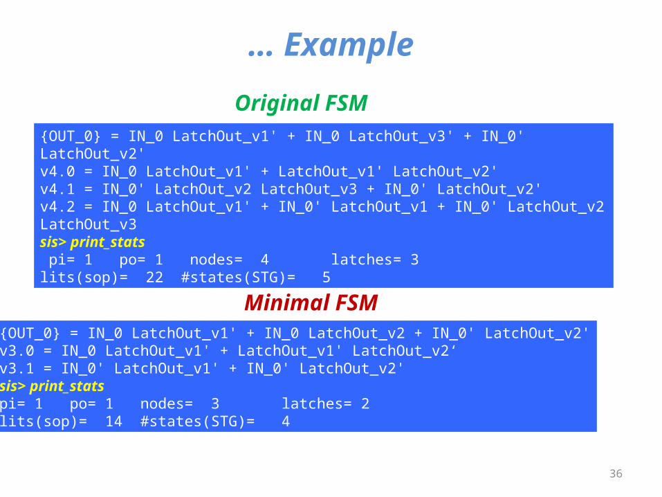
{OUT_0} = IN_0 LatchOut_v1' + IN_0 LatchOut_v3' + IN_0' LatchOut_v2'v4.0 = IN_0 LatchOut_v1' + LatchOut_v1' LatchOut_v2'v4.1 = IN_0' LatchOut_v2 LatchOut_v3 + IN_0' LatchOut_v2'v4.2 = IN_0 LatchOut_v1' + IN_0' LatchOut_v1 + IN_0' LatchOut_v2 LatchOut_v3sis> print_stats pi= 1 po= 1 nodes= 4 latches= 3lits(sop)= 22 #states(STG)= 5
{OUT_0} = IN_0 LatchOut_v1' + IN_0 LatchOut_v2 + IN_0' LatchOut_v2'v3.0 = IN_0 LatchOut_v1' + LatchOut_v1' LatchOut_v2‘v3.1 = IN_0' LatchOut_v1' + IN_0' LatchOut_v2'sis> print_statspi= 1 po= 1 nodes= 3 latches= 2lits(sop)= 14 #states(STG)= 4
Original FSM
Minimal FSM
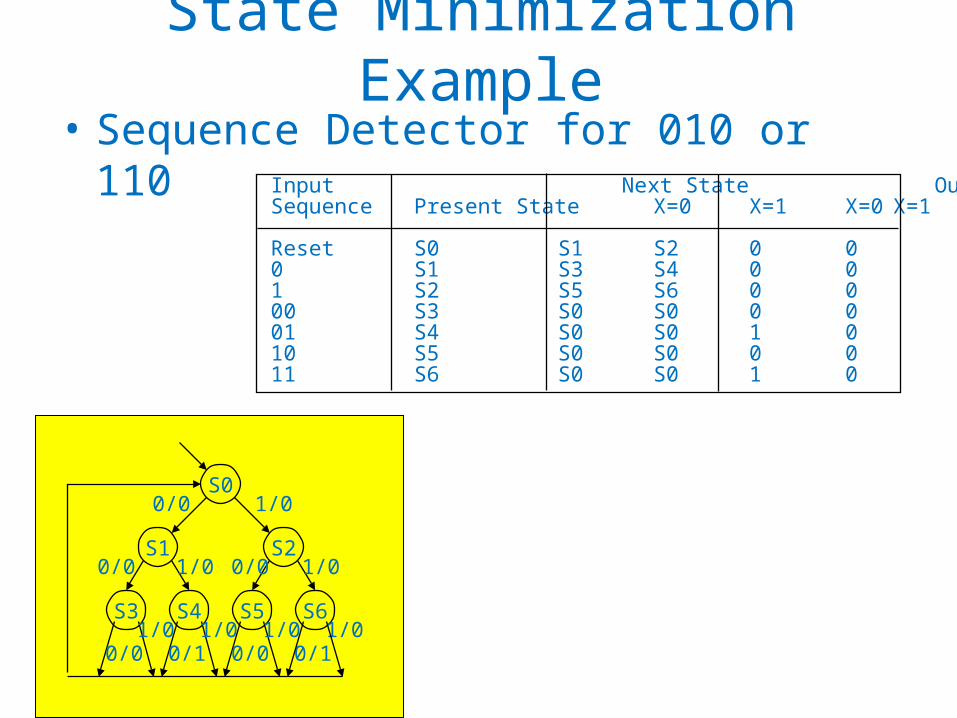
Input Next State OutputSequence Present StateX=0 X=1 X=0 X=1
Reset S0 S1 S2 0 00 S1 S3 S4 0 01 S2 S5 S6 0 000 S3 S0 S0 0 001 S4 S0 S0 1 010 S5 S0 S0 0 011 S6 S0 S0 1 0
State Minimization Example• Sequence Detector for 010 or 110
S0
S3
S2S1
S5 S6S4
1/00/0
1/0
1/00/1
0/01/00/0
1/00/0
1/00/1
1/00/0

( S0 S1 S2 S3 S4 S5 S6 )
( S0 S1 S2 S3 S5 ) ( S4 S6 )
( S0 S1 S2 ) ( S3 S5 ) ( S4 S6 )
( S0 ) ( S1 S2 ) ( S3 S5 ) ( S4 S6 )
Input Next State OutputSequence Present StateX=0 X=1 X=0 X=1
Reset S0 S1 S2 0 00 S1 S3 S4 0 01 S2 S5 S6 0 000 S3 S0 S0 0 001 S4 S0 S0 1 010 S5 S0 S0 0 011 S6 S0 S0 1 0
S1 is equivalent to S2
S3 is equivalent to S5
S4 is equivalent to S6
Method of Successive Partitions

Input Next State OutputSequence Present State X=0 X=1 X=0 X=1
Reset S0 S1' S1' 0 00 + 1 S1' S3' S4' 0 0X0 S3' S0 S0 0 0X1 S4' S0 S0 1 0
Minimized FSM
State minimized sequence detector for 010 or 110
S0
S1’
S3’ S4’
X/0
1/0
1/00/1
0/0
X/0

40
Computational Complexity
• Polynomially-bound algorithm.
• There can be at most |S| partition refinements.• Each refinement requires considering each state
– Complexity O(|S|2).
• Actual time may depend upon– Data-structures.– Implementation details.

Implication Table Method
41
A B C D E F G H
B
C
D
E
F
G
H
I EGAH
Present state
Next state, output (Z)
InputI1 I2
A D / 0 C / 1
B E / 1 A / 1
C H / 1 D / 1
D D / 0 C / 1
E B / 0 G / 1
F H / 1 D / 1
G A / 0 F /1
H C / 0 A / 1
I G / 1 H / 1
GHDH
GHDH
√BDCG
ADCF
√
CDAC
EHAD
EHAD
ADCF
CDAC
BCAG
BDCG
ACAF
ABFG

Implication Table Method (Cont.)
42
A B C D E F G H
B
C
D
E
F
G
H
I
√BDCG
ADCF
√
CDAC
EHAD
EHAD
EGAH
ADCF
CDAC
BCAG
BDCG
ACAF
GHDH
GHDH
Equivalent states:
S1: A, D, G
S2: B, C, F
S3: E, H
S4: IABFG
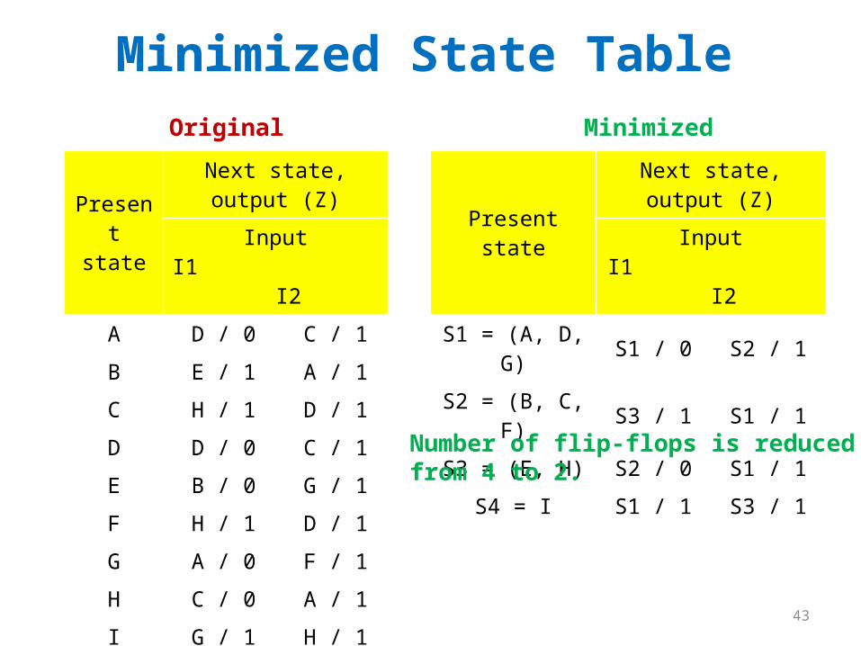
Minimized State Table
43
Present state
Next state, output (Z)
InputI1 I2
A D / 0 C / 1
B E / 1 A / 1
C H / 1 D / 1
D D / 0 C / 1
E B / 0 G / 1
F H / 1 D / 1
G A / 0 F / 1
H C / 0 A / 1
I G / 1 H / 1
Present stateNext state, output (Z)
InputI1 I2
S1 = (A, D, G) S1 / 0 S2 / 1
S2 = (B, C, F) S3 / 1 S1 / 1
S3 = (E, H) S2 / 0 S1 / 1
S4 = I S1 / 1 S3 / 1
Original Minimized
Number of flip-flops is reducedfrom 4 to 2.

Incompletely Specified Machines
• Next state and output functions have don’t cares. • However, for an implementation, and are functions,
– thus they are uniquely defined for each input and state combination.
• Don’t cares arise when some combinations are of no interest:– they will not occur or– their outputs will not be observed
• For these, the next state or output may not be specified. – (In this case, and are relations, but of special type. We should
make sure we want these as don’t cares.)
• Such machines are called incompletely specified.

45
… State Minimizationfor Incompletely Specified FSMs
• Minimum finite-state machine is not unique.• Implication relations make problem intractable.• Example
– Replace * by 1.• {(s1, s2), (s3), (s4), (s5)}.
Minimized to 4 states

46
… State Minimizationfor Incompletely Specified FSMs
• Minimum finite-state machine is not unique.• Example
– Replace * by 0.• {(s1, s5), (s2, s3, s4)}.
00
It is now completely specified
Unfortunately, there is an exponentialnumber of completely specified FSMsin correspondence to the choice of thedon’t care values!!

Example
By adding a dummy state this can be converted to a machine with only the output incompletely specified.
Could also specify “error” as the output when transitioning to the dummy state.
Alternatively (better for optimization), can interpret undefined next state as allowing any next state.
s1 s2
1/1
1/-
0/0
s1 s2
1/1
1/-
0/00/- 0/-
s1 s2
1/1
1/-
0/0
d
0/-
-/-
added dummynon-acceptingstate
added transitionsto all states andoutput any value

48
State Encoding• Binary and Gray encoding use the minimum
number of bits for state register• Gray and Johnson code:
– Two adjacent codes differ by only one bit• Reduce simultaneous switching
– Reduce crosstalk– Reduce glitch
# Binary Gray Johnson One-hot
0 000 000 0000 00000001
1 001 001 0001 00000010
2 010 011 0011 00000100
3 011 010 0111 00001000
4 100 110 1111 00010000
5 101 111 1110 00100000
6 110 101 1100 01000000
7 111 100 1000 10000000

49
State Encoding
• The cost & delay of FSM implementation depends on encoding of symbolic states.– e.g., 4 states can be encoded in 4! = 24 different ways
• There are more than n! different encodings for n states.– exploration of all encodings is impossible, therefore
heuristics are used• Heuristics Used:
1. One-hot encoding2. minimum-bit change3. prioritized adjacency

50
One-hot Encoding
• Uses redundant encoding in which one flip-flop is assigned to each state.
• Each state is distinguishable by its own flip-flop having a value of 1 while all others have a value of 0.
A B C
S = 0
S = 1
Z = 0
Z = 1
A 00
S0 1
B
C
01
10
Z0 1
51
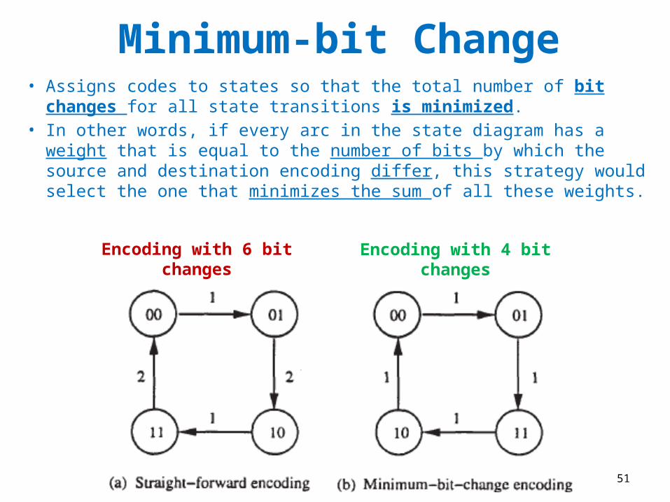
Minimum-bit Change• Assigns codes to states so that the total number of bit changes for all
state transitions is minimized.• In other words, if every arc in the state diagram has a weight that is
equal to the number of bits by which the source and destination encoding differ, this strategy would select the one that minimizes the sum of all these weights.
Encoding with 6 bitchanges
Encoding with 4 bitchanges

1 1 1
1 1 1
1 1 1
1 1
The Idea of Adjacency• Inputs are A and B• State variables are Y1 and Y2• An output is F(A, B, Y1, Y2)• A next state function is G(A, B, Y1, Y2)
52
A
B
Y1
Y2
Karnaugh map ofoutput function ornext state function
Larger clustersproduce smaller logic function.
Clustered mintermsdiffer in one variable.

Size of an Implementation• Number of product terms determines number of gates.• Number of literals in a product term determines
number of gate inputs, which is proportional to number of transistors.
• Hardware α (total number of literals)• Examples of four minterm functions:
• F1 = ABCD +ABCD +ABCD +ABCD has 16 literals• F2 = ABC +ACD has 6 literals
53

Rule 1 (Priority #1), Common DestStates that have the same next state for some fixed input should be assigned logically adjacent codes.
54
Combinational logic
Flip-flops
OutputsFixedInputs
Presentstate
Nextstate
ClockClear
Si
Sj
Sk
Rule #1: (S1, S2)
The input value of 0 will move both states into the same state S3
S0
S3 S2
S1
0/0
0/1
0/01/0
0/1, 1/1

Rule 2 (Priority #2), A Common Source
States that are the next states of the same state under logically adjacent inputs, should be assigned logically adjacent codes.
55
Combinational logic
Flip-flops
OutputsAdjacentInputs
Fixedpresent
state
Nextstate
ClockClear
SkSm
Si
I1I2
S0
S3 S2
S1
0/0
0/1
0/01/0
0/1, 1/1
Rule #2: (S1, S2)
They are both next states of the state S0

Rule 3 (Priority #3), A Common Output
States that have the same output value for the same input value, should be assigned logically adjacent codes.
56
Combinational logic
Flip-flops
OutputsAdjacentInputs
Fixedpresent
state
Nextstate
ClockClear
SkSm
Si
I1I2
S0
S3 S2
S1
0/0
0/1
0/01/0
0/1, 1/1
01
00 10
110/0
0/1
0/01/0
0/1, 1/1
Rule #3: (S0, S1), and (S2, S3), states S0 and S1 have the same output value 0 for the same input value 0

Example of State Assignment
57
Present state
Next state, output (Z)
Input, X0 1
A C, 0 D, 0B C, 0 A, 0C B, 0 D, 0D A, 1 B, 1
D B
A
C
0/0
0/0
0/0
1/01/0
1/0
1/1
0/1
A adj B(Rule 1)
A adj C(Rule 1)
B adj D(Rule 2)
C adj D(Rule 2)
A B
C D
0 1
0
1
Verify that BC andAD are not adjacent.
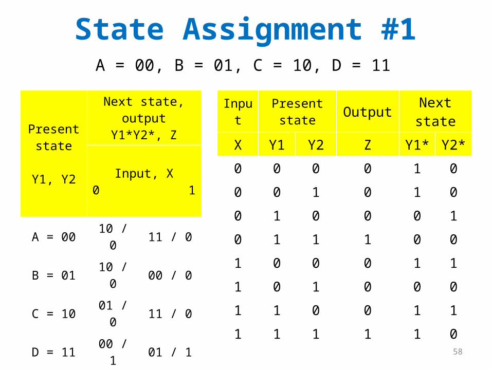
State Assignment #1
58
Present state
Y1, Y2
Next state, outputY1*Y2*, Z
Input, X0 1
A = 00 10 / 0 11 / 0B = 01 10 / 0 00 / 0C = 10 01 / 0 11 / 0D = 11 00 / 1 01 / 1
Input Present state Output Next state
X Y1 Y2 Z Y1* Y2*
0 0 0 0 1 0
0 0 1 0 1 0
0 1 0 0 0 1
0 1 1 1 0 0
1 0 0 0 1 1
1 0 1 0 0 0
1 1 0 0 1 1
1 1 1 1 1 0
A = 00, B = 01, C = 10, D = 11
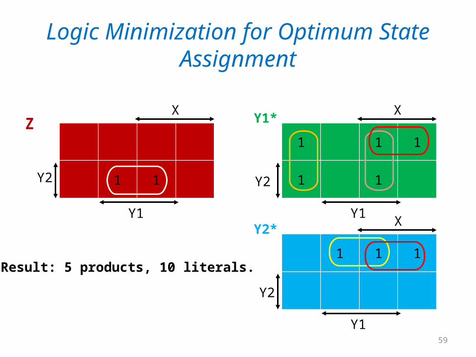
Logic Minimization for Optimum State Assignment
59
1 1 1
1 1Y2
X
Y1
1 1 1
Y2
Y1
1 1Y2
X
Y1X
Z Y1*
Y2*
Result: 5 products, 10 literals.
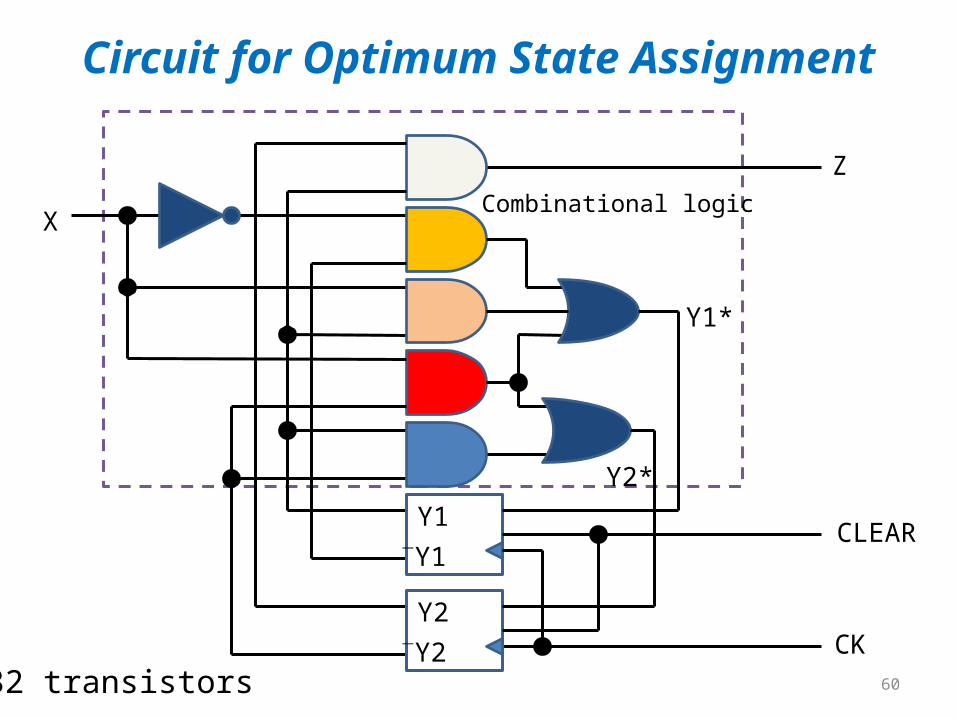
Circuit for Optimum State Assignment
60
Y2
Y1
Y1
Y2
X
Z
Y2*
Y1*
CK
CLEAR
Combinational logic
32 transistors

Using an Arbitrary State Assignment: A = 00, B = 01, C = 11, D = 10
61
Present state
Y1, Y2
Next state, outputY1*Y2*, Z
Input, X0 1
A = 00 11 / 0 10 / 0B = 01 11 / 0 00 / 0C = 11 01 / 0 10 / 0D = 10 00 / 1 01 / 1
Input Present state Output Next state
X Y1 Y2 Z Y1* Y2*
0 0 0 0 1 1
0 0 1 0 1 1
0 1 0 1 0 0
0 1 1 0 0 1
1 0 0 0 1 0
1 0 1 0 0 0
1 1 0 1 0 1
1 1 1 0 1 0

Logic Minimization for Arbitrary State Assignment
62
Current Result: 6 products, 14 literals.
1 1
1 1Y2
X
1 1
Y2
XZ Y1*
1 1
1 1Y2
Y1
XY2*
Y1 Y1
Previous Result: 5 products, 10 literals.

Circuit for Arbitrary State Assignment
63
Y2
Y1
Y1
Y2
X
Z
Y2*
Y1*
CK
CLEAR
Comb.logic
42 transistors

64
Best Encoding Strategy• To determine the
encoding with the minimum cost and delay, we need to:
1. Generate K-Maps for the next-state and output functions
2. Derive excitation equations from the next-state map.
3. Derive output equations from the output function map.
4. Implement above equations using two-level NAND gates.
5. Calculate cost and delay

65
Optimizing Sequential Circuits by Retiming Netlist of Gates
Netlist of gates and registers:
Various Goals:– Reduce clock cycle time– Reduce area
• Reduce number of latches
Inputs
Outputs
66
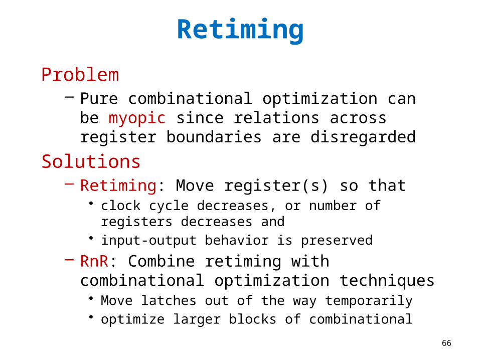
Retiming
Problem– Pure combinational optimization can be
myopic since relations across register boundaries are disregarded
Solutions– Retiming: Move register(s) so that
• clock cycle decreases, or number of registers decreases and
• input-output behavior is preserved– RnR: Combine retiming with combinational
optimization techniques • Move latches out of the way temporarily• optimize larger blocks of combinational
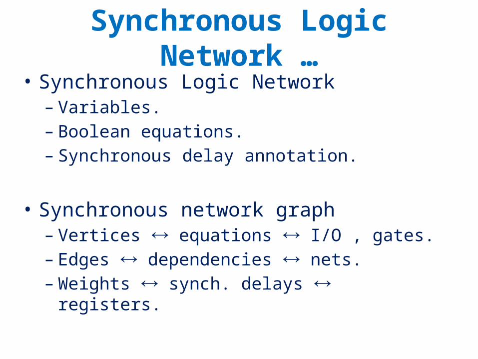
Synchronous Logic Network …• Synchronous Logic Network
– Variables.– Boolean equations.– Synchronous delay annotation.
• Synchronous network graph– Vertices equations I/O , gates.– Edges dependencies nets.– Weights synch. delays registers.

68
Circuit Representation
Circuit representation: G(V,E,d,w)– V set of gates– E set of wires– d(v) = delay of gate/vertex v, (d(v)0)– w(e) = number of registers on edge e,
(w(e)0)

… Synchronous Logic Network

70
Circuit RepresentationExample: Correlator (from Leiserson and Saxe) (simplified)
Circuit
(x, y) = 1 if x=y0 otherwise
Operation delay
3
+ 7
Every cycle in Graph has at least one register i.e. no combinational loops.
0
3 3
0
00
02
Retiming Graph (Directed)
7
a b
+
Host

71
Preliminaries
For a path p :
Clock cycle
1
0
0
)()(
)()(
k
ii
k
ii
ewpw
vdpd endpoints) (includes
: ( ) 0max { ( )}p w p
c d p
For correlator c = 13
Path with
w(p)=00
3 3
0
00
02
7
0 11
0 1 1
ke ee
k kv v v v
Path Delay
Path weight
72
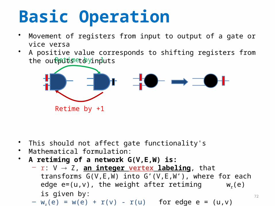
• Movement of registers from input to output of a gate or vice versa• A positive value corresponds to shifting registers from the outputs to inputs
• This should not affect gate functionality's• Mathematical formulation:• A retiming of a network G(V,E,W) is:
– r: V Z, an integer vertex labeling, that transforms G(V,E,W) into G’(V,E,W’), where for each edge e=(u,v), the weight after retiming wr(e) is given by:
– wr(e) = w(e) + r(v) - r(u) for edge e = (u,v)
Basic Operation
Retime by +1
Retime by -1
73
Sequential Logic Synthesis is an important phase of the Front End Tool for VLSI Circuits.
Optimization of Sequential Circuits involves: State Minimization State Encoding Retiming
State Minimization may be applied to completely specified Machines or Incompletely specified Machines.
State Encoding utilizes different heuristics to further minimize the logic
Retiming plays an important role in reducing the latency of the circuit.
Summary

74
Related Documents