Ultramicroscopy 96 (2003) 481–489 Energy-filtering TEM at high magnification: spatial resolution and detection limits Werner Grogger a, *, Bernhard Schaffer a , Kannan M. Krishnan b , Ferdinand Hofer a a Research Institute for Electron Microscopy, Graz University of Technology, Steyrergasse 17, Graz A-8010, Austria b Lawrence Berkeley National Lab., NCEM, Materials Sciences Div., Berkeley, CA 94720, USA Received 15 August 2002; accepted 3 November 2002 Abstract Energy-filtering TEM (EFTEM) has turned out to be a very efficient and rapid tool for the chemical characterization of a specimen on a nanometer and even subnanometer length scale. Especially, the detection and measurement of very thin layers has become a great application of this technique in many materials science fields, e.g. semiconductors and hard disk technology. There, the reliability of compositional profiles is an important issue. However, the experimentally obtainable spatial resolution strongly influences the appearance of a thin layer in an EFTEM image, when dimensions reach subnanometer levels, which mainly leads to a broadening of the layer in the image. This fact has to be taken into account, when measuring the thickness of such a thin layer. Additionally, the convolution decreases contrast which makes the layer less visible in the image and finally determines the detection limit. In this work we present a systematic study on specifically designed Mn/PdMn multilayer test specimens to explore the practical aspects of spatial resolution and detection limits in EFTEM. Although specific to the ionization edges used, we will present general conclusions about the practical limitations in terms of EFTEM spatial resolution. Additionally, work will be shown about low energy-loss imaging of thin oxide layers, where delocalization is the main factor responsible for broadening. r 2003 Elsevier Science B.V. All rights reserved. Keywords: Energy-filtering TEM; Spatial resolution; Detection limit 1. Introduction The applications of transmission electron micro- scopy (TEM) are more and more focusing on investigations on a nanometer length scale and beyond. Besides structural information from high resolution TEM (HRTEM), analytical informa- tion at these dimensions is in many cases paramount to the understanding of macroscopic functional properties of many modern materials science specimens. In semiconductor industry miniaturization de- creases layer thicknesses down to just a few nanometers, for instance for the gate oxide layers. The quality of these layers, like thickness and homogeneity, is directly related to device ARTICLE IN PRESS *Corresponding author. Tel.: +43-316-873-8323; fax: +43- 316-811596. E-mail address: [email protected] (W. Grogger). 0304-3991/03/$ - see front matter r 2003 Elsevier Science B.V. All rights reserved. doi:10.1016/S0304-3991(03)00110-4

Welcome message from author
This document is posted to help you gain knowledge. Please leave a comment to let me know what you think about it! Share it to your friends and learn new things together.
Transcript
Ultramicroscopy 96 (2003) 481–489
Energy-filtering TEM at high magnification: spatial resolutionand detection limits
Werner Groggera,*, Bernhard Schaffera, Kannan M. Krishnanb, Ferdinand Hofera
aResearch Institute for Electron Microscopy, Graz University of Technology, Steyrergasse 17, Graz A-8010, AustriabLawrence Berkeley National Lab., NCEM, Materials Sciences Div., Berkeley, CA 94720, USA
Received 15 August 2002; accepted 3 November 2002
Abstract
Energy-filtering TEM (EFTEM) has turned out to be a very efficient and rapid tool for the chemical characterization
of a specimen on a nanometer and even subnanometer length scale. Especially, the detection and measurement of very
thin layers has become a great application of this technique in many materials science fields, e.g. semiconductors and
hard disk technology. There, the reliability of compositional profiles is an important issue. However, the experimentally
obtainable spatial resolution strongly influences the appearance of a thin layer in an EFTEM image, when dimensions
reach subnanometer levels, which mainly leads to a broadening of the layer in the image. This fact has to be taken into
account, when measuring the thickness of such a thin layer. Additionally, the convolution decreases contrast which
makes the layer less visible in the image and finally determines the detection limit.
In this work we present a systematic study on specifically designed Mn/PdMn multilayer test specimens to explore the
practical aspects of spatial resolution and detection limits in EFTEM. Although specific to the ionization edges used, we
will present general conclusions about the practical limitations in terms of EFTEM spatial resolution. Additionally,
work will be shown about low energy-loss imaging of thin oxide layers, where delocalization is the main factor
responsible for broadening.
r 2003 Elsevier Science B.V. All rights reserved.
Keywords: Energy-filtering TEM; Spatial resolution; Detection limit
1. Introduction
The applications of transmission electron micro-scopy (TEM) are more and more focusing oninvestigations on a nanometer length scale andbeyond. Besides structural information from high
resolution TEM (HRTEM), analytical informa-tion at these dimensions is in many casesparamount to the understanding of macroscopicfunctional properties of many modern materialsscience specimens.In semiconductor industry miniaturization de-
creases layer thicknesses down to just a fewnanometers, for instance for the gate oxide layers.The quality of these layers, like thicknessand homogeneity, is directly related to device
ARTICLE IN PRESS
*Corresponding author. Tel.: +43-316-873-8323; fax: +43-
316-811596.
E-mail address: [email protected] (W. Grogger).
0304-3991/03/$ - see front matter r 2003 Elsevier Science B.V. All rights reserved.
doi:10.1016/S0304-3991(03)00110-4
performance, and therefore needs to be determinedaccurately. In many fields small particles with thinsurface layers play an important role (e.g. cata-lysts), where the analytical characterization ofthese layers and their dimensions is of greatimportance. Fine-grained materials exhibit grainsizes down to some ten nanometers, and are inmany cases synthesized by adding small amountsof dopants. These dopants were shown to formmonolayer thin phases at the grain boundaries.Furthermore, small inclusions and precipitates innanocomposites determine the macroscopic beha-vior of these materials, which also need a careful,accurate, and reliable characterization. In all ofthese applications it is important to determine themorphology as well as the chemistry of thematerials investigated.During the last decade, energy-filtering TEM
(EFTEM) has proven to be a powerful analyticalmethod with its resolution reaching atomic levels.Using this technique, chemical information canrather easily be obtained for all different kinds ofmaterials. From such elemental distributionimages critical dimensions of the chemical phasesinvolved can be determined. However, measuringsmall dimensions accurately from EFTEM imagesrequires some caution, as the obtainable EFTEMresolution tends to broaden features to a certainextent and also strongly influences the detectionlimits. This paper describes how the terms ‘‘spatialresolution’’ and ‘‘detection limit’’ can be under-stood in relation to EFTEM imaging, and showshow these terms relate to each other. Twoapplication examples demonstrate the capabilitiesof EFTEM with regard to resolution and detectionlimit.
2. Theoretical considerations
In EFTEM, post-column energy filters incombination with high resolution TEMs canprovide the capability to detect small features,like thin layers or small particles, down tosubnanometer dimensions [1–10]. (Other groupsalso tried to reach nm-resolution but either theresults were contradictory or not quite unequi-vocal [11–13].) Often this detection capability is
used to describe the spatial resolution of thetechnique. When talking about spatial resolutionin electron microscopy, in most cases ‘‘minimumresolvable distance’’ is meant. Therefore, it shouldbe recalled, that the term ‘‘spatial resolution’’ ismostly understood as the minimum distancebetween two objects at which they can still beseparated. For the definition of this term, Ray-leigh’s criterion may be used. There, the minimumresolvable distance is defined as the distancebetween two objects at which the first diffractionminimum of one overlaps with the first maximumof the other. This definition is equivalent to acontrast drop between the two objects to 73.6% ofthe maximum. Contrarily, a term like ‘‘detectioncapability’’ should be used for the ability to detectsmall objects.Far more than in high-resolution TEM, the
attainable spatial resolution in EFTEM is influ-enced by the experimental setup: The energy andthe shape of the ionization edge, as well asexperimental parameters like the collection angle,influence the obtainable resolution together withinstrumental parameters (aberration coefficients ofthe TEM objective lens) [6,14,15]. For instance,delocalization is one of the main factors influen-cing spatial resolution at low energy-losses.Additionally to these theoretical limitations,
however, there are practical aspects, that also limitthe resolution in EFTEM: maximum electrondose, exposure time, specimen drift and instru-mental instabilities. When considering, that at highmagnifications only a small number of atoms(typically 10–1000) contribute to the signal in apixel of the final image, it is obvious that accurateinstrumental alignments and a careful experimen-tal setup are paramount for good quality results. Itshould also be noted, that a certain amount ofelastic contrast is always transferred to energy-filtered images [15], which can lead to artifacts inelemental distribution images. According to theformulae given in the literature e.g. [6,14] theobtainable spatial resolution in an EFTEM imagecan be computed. Typical values range from acouple of tenths of a nanometer to a fewnanometers.The dimension of a small object in an EFTEM
image is therefore a convolution of the real size
ARTICLE IN PRESS
W. Grogger et al. / Ultramicroscopy 96 (2003) 481–489482
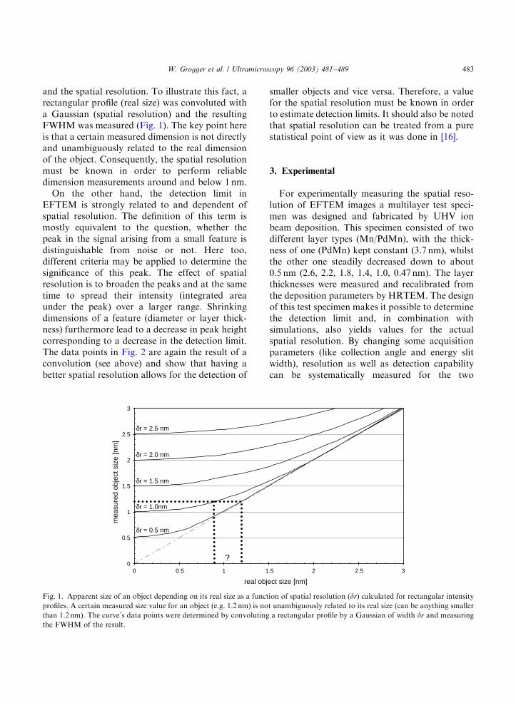
and the spatial resolution. To illustrate this fact, arectangular profile (real size) was convoluted witha Gaussian (spatial resolution) and the resultingFWHM was measured (Fig. 1). The key point hereis that a certain measured dimension is not directlyand unambiguously related to the real dimensionof the object. Consequently, the spatial resolutionmust be known in order to perform reliabledimension measurements around and below 1 nm.On the other hand, the detection limit in
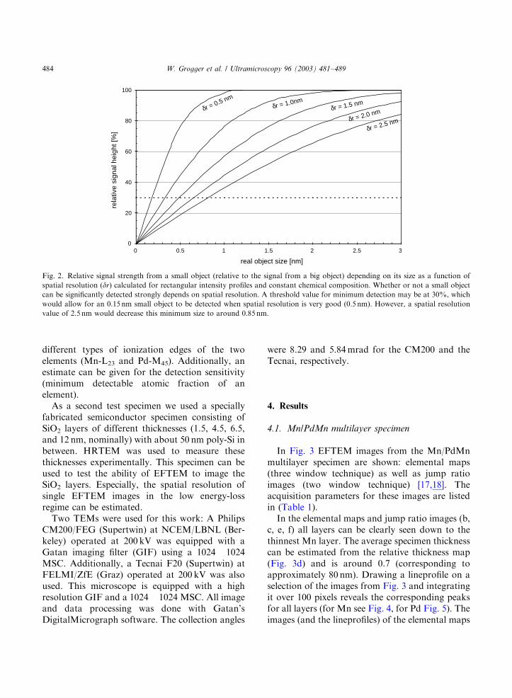
EFTEM is strongly related to and dependent ofspatial resolution. The definition of this term ismostly equivalent to the question, whether thepeak in the signal arising from a small feature isdistinguishable from noise or not. Here too,different criteria may be applied to determine thesignificance of this peak. The effect of spatialresolution is to broaden the peaks and at the sametime to spread their intensity (integrated areaunder the peak) over a larger range. Shrinkingdimensions of a feature (diameter or layer thick-ness) furthermore lead to a decrease in peak heightcorresponding to a decrease in the detection limit.The data points in Fig. 2 are again the result of aconvolution (see above) and show that having abetter spatial resolution allows for the detection of
smaller objects and vice versa. Therefore, a valuefor the spatial resolution must be known in orderto estimate detection limits. It should also be notedthat spatial resolution can be treated from a purestatistical point of view as it was done in [16].
3. Experimental
For experimentally measuring the spatial reso-lution of EFTEM images a multilayer test speci-men was designed and fabricated by UHV ionbeam deposition. This specimen consisted of twodifferent layer types (Mn/PdMn), with the thick-ness of one (PdMn) kept constant (3.7 nm), whilstthe other one steadily decreased down to about0.5 nm (2.6, 2.2, 1.8, 1.4, 1.0, 0.47 nm). The layerthicknesses were measured and recalibrated fromthe deposition parameters by HRTEM. The designof this test specimen makes it possible to determinethe detection limit and, in combination withsimulations, also yields values for the actualspatial resolution. By changing some acquisitionparameters (like collection angle and energy slitwidth), resolution as well as detection capabilitycan be systematically measured for the two
ARTICLE IN PRESS
0 0.5 1 1.5 2 2.5 3
real object size [nm]
0
0.5
1
1.5
2
2.5
3
mea
sure
d ob
ject
siz
e [n
m]
δr = 2.5 nm
δr = 2.0 nm
δr = 1.5 nm
δr = 1.0nm
δr = 0.5 nm
?
Fig. 1. Apparent size of an object depending on its real size as a function of spatial resolution (dr) calculated for rectangular intensity
profiles. A certain measured size value for an object (e.g. 1.2 nm) is not unambiguously related to its real size (can be anything smaller
than 1.2 nm). The curve’s data points were determined by convoluting a rectangular profile by a Gaussian of width dr and measuring
the FWHM of the result.
W. Grogger et al. / Ultramicroscopy 96 (2003) 481–489 483
different types of ionization edges of the twoelements (Mn-L23 and Pd-M45). Additionally, anestimate can be given for the detection sensitivity(minimum detectable atomic fraction of anelement).As a second test specimen we used a specially
fabricated semiconductor specimen consisting ofSiO2 layers of different thicknesses (1.5, 4.5, 6.5,and 12 nm, nominally) with about 50 nm poly-Si inbetween. HRTEM was used to measure thesethicknesses experimentally. This specimen can beused to test the ability of EFTEM to image theSiO2 layers. Especially, the spatial resolution ofsingle EFTEM images in the low energy-lossregime can be estimated.Two TEMs were used for this work: A Philips
CM200/FEG (Supertwin) at NCEM/LBNL (Ber-keley) operated at 200 kV was equipped with aGatan imaging filter (GIF) using a 1024� 1024MSC. Additionally, a Tecnai F20 (Supertwin) atFELMI/ZfE (Graz) operated at 200 kV was alsoused. This microscope is equipped with a highresolution GIF and a 1024� 1024 MSC. All imageand data processing was done with Gatan’sDigitalMicrograph software. The collection angles
were 8.29 and 5.84mrad for the CM200 and theTecnai, respectively.
4. Results
4.1. Mn/PdMn multilayer specimen
In Fig. 3 EFTEM images from the Mn/PdMnmultilayer specimen are shown: elemental maps(three window technique) as well as jump ratioimages (two window technique) [17,18]. Theacquisition parameters for these images are listedin (Table 1).In the elemental maps and jump ratio images (b,
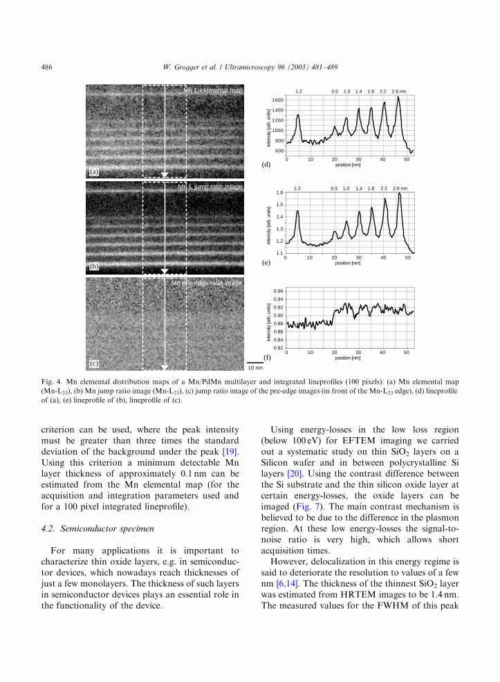
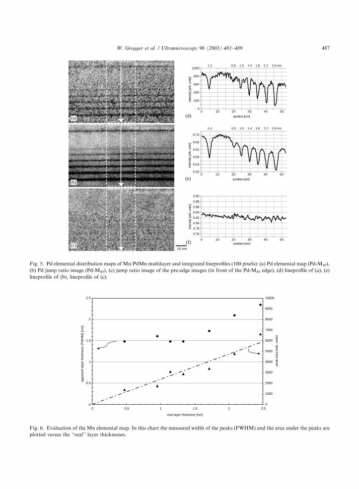
c, e, f) all layers can be clearly seen down to thethinnest Mn layer. The average specimen thicknesscan be estimated from the relative thickness map(Fig. 3d) and is around 0.7 (corresponding toapproximately 80 nm). Drawing a lineprofile on aselection of the images from Fig. 3 and integratingit over 100 pixels reveals the corresponding peaksfor all layers (for Mn see Fig. 4, for Pd Fig. 5). Theimages (and the lineprofiles) of the elemental maps
ARTICLE IN PRESS
0 0.5 1 1.5 2 2.5 3
real object size [nm]
0
20
40
60
80
100
rela
tive
sign
al h
eigh
t [%
] δr = 2.5 nmδr = 2.0 nmδr = 1.5 nmδr = 1.0nm
δr = 0.5 nm
Fig. 2. Relative signal strength from a small object (relative to the signal from a big object) depending on its size as a function of
spatial resolution (dr) calculated for rectangular intensity profiles and constant chemical composition. Whether or not a small object
can be significantly detected strongly depends on spatial resolution. A threshold value for minimum detection may be at 30%, which
would allow for an 0.15 nm small object to be detected when spatial resolution is very good (0.5 nm). However, a spatial resolution
value of 2.5 nm would decrease this minimum size to around 0.85 nm.
W. Grogger et al. / Ultramicroscopy 96 (2003) 481–489484
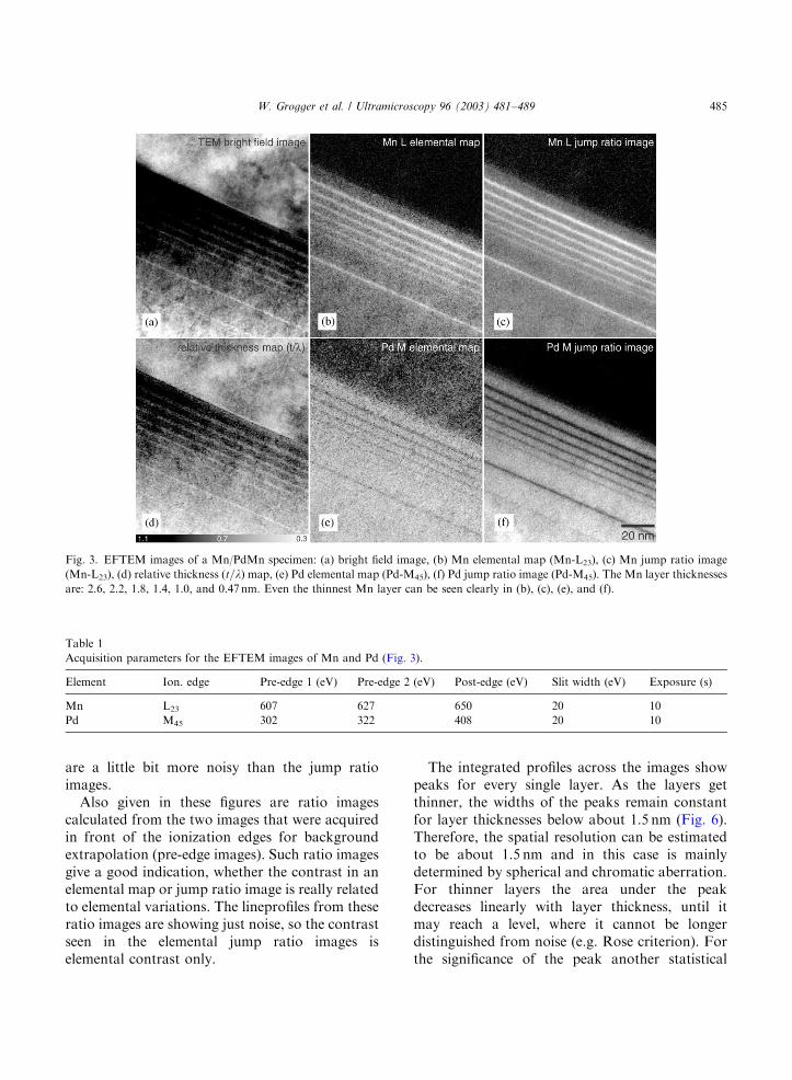
are a little bit more noisy than the jump ratioimages.Also given in these figures are ratio images
calculated from the two images that were acquiredin front of the ionization edges for backgroundextrapolation (pre-edge images). Such ratio imagesgive a good indication, whether the contrast in anelemental map or jump ratio image is really relatedto elemental variations. The lineprofiles from theseratio images are showing just noise, so the contrastseen in the elemental jump ratio images iselemental contrast only.
The integrated profiles across the images showpeaks for every single layer. As the layers getthinner, the widths of the peaks remain constantfor layer thicknesses below about 1.5 nm (Fig. 6).Therefore, the spatial resolution can be estimatedto be about 1.5 nm and in this case is mainlydetermined by spherical and chromatic aberration.For thinner layers the area under the peakdecreases linearly with layer thickness, until itmay reach a level, where it cannot be longerdistinguished from noise (e.g. Rose criterion). Forthe significance of the peak another statistical
ARTICLE IN PRESS
Fig. 3. EFTEM images of a Mn/PdMn specimen: (a) bright field image, (b) Mn elemental map (Mn-L23), (c) Mn jump ratio image
(Mn-L23), (d) relative thickness (t=l) map, (e) Pd elemental map (Pd-M45), (f) Pd jump ratio image (Pd-M45). The Mn layer thicknesses
are: 2.6, 2.2, 1.8, 1.4, 1.0, and 0.47 nm. Even the thinnest Mn layer can be seen clearly in (b), (c), (e), and (f).
Table 1
Acquisition parameters for the EFTEM images of Mn and Pd (Fig. 3).
Element Ion. edge Pre-edge 1 (eV) Pre-edge 2 (eV) Post-edge (eV) Slit width (eV) Exposure (s)
Mn L23 607 627 650 20 10
Pd M45 302 322 408 20 10
W. Grogger et al. / Ultramicroscopy 96 (2003) 481–489 485
criterion can be used, where the peak intensitymust be greater than three times the standarddeviation of the background under the peak [19].Using this criterion a minimum detectable Mnlayer thickness of approximately 0.1 nm can beestimated from the Mn elemental map (for theacquisition and integration parameters used andfor a 100 pixel integrated lineprofile).
4.2. Semiconductor specimen
For many applications it is important tocharacterize thin oxide layers, e.g. in semiconduc-tor devices, which nowadays reach thicknesses ofjust a few monolayers. The thickness of such layersin semiconductor devices plays an essential role inthe functionality of the device.
Using energy-losses in the low loss region(below 100 eV) for EFTEM imaging we carriedout a systematic study on thin SiO2 layers on aSilicon wafer and in between polycrystalline Silayers [20]. Using the contrast difference betweenthe Si substrate and the thin silicon oxide layer atcertain energy-losses, the oxide layers can beimaged (Fig. 7). The main contrast mechanism isbelieved to be due to the difference in the plasmonregion. At these low energy-losses the signal-to-noise ratio is very high, which allows shortacquisition times.However, delocalization in this energy regime is
said to deteriorate the resolution to values of a fewnm [6,14]. The thickness of the thinnest SiO2 layerwas estimated from HRTEM images to be 1.4 nm.The measured values for the FWHM of this peak
ARTICLE IN PRESS
10 nm
600
800
1000
1200
1400
1600
0 10 20 30 40 50position [nm]
inte
nsity
[arb
. uni
ts]
0 10 20 30 40 50position [nm]
1.2
1.6
1.5
1.4
1.3
1.1
inte
nsity
[arb
. uni
ts]
0 10 20 30 40 50position [nm]
0.96
0.94
0.92
0.90
0.88
0.86
0.84
0.82
inte
nsity
[arb
. uni
ts]
Mn L jump ratio image
Mn L elemental map
Mn pre-edge ratio image
1.2 0.5 1.0 1.4 1.8 2.2 2.6 nm
1.2 0.5 1.0 1.4 1.8 2.2 2.6 nm
(a)
(b)
(c)
(d)
(e)
(f)
Fig. 4. Mn elemental distribution maps of a Mn/PdMn multilayer and integrated lineprofiles (100 pixels): (a) Mn elemental map
(Mn-L23), (b) Mn jump ratio image (Mn-L23), (c) jump ratio image of the pre-edge images (in front of the Mn-L23 edge), (d) lineprofile
of (a), (e) lineprofile of (b), lineprofile of (c).
W. Grogger et al. / Ultramicroscopy 96 (2003) 481–489486
ARTICLE IN PRESS
10 nm
0 10 20 30 40 50
position [nm]
0
200
400
600
800
1000
inte
nsity
[arb
. uni
ts]
0 10 20 30 40 50
position [nm]
0.70
0.66
0.62
0.58
0.54
0.50
inte
nsity
[arb
. uni
ts]
0 10 20 30 40 50position [nm]
0.90
0.88
0.86
0.84
0.82
0.80
0.78
0.76
inte
nsity
[arb
. uni
ts]
Pd M elemental map
Pd M jump ratio image
Pd pre-edge ratio image
1.2 0.5 1.0 1.4 1.8 2.2 2.6 nm
1.2 0.5 1.0 1.4 1.8 2.2 2.6 nm
(a)
(b)
(c)
(d)
(e)
(f)
Fig. 5. Pd elemental distribution maps of Mn/PdMn multilayer and integrated lineprofiles (100 pixels): (a) Pd elemental map (Pd-M45),
(b) Pd jump ratio image (Pd-M45), (c) jump ratio image of the pre-edge images (in front of the Pd-M45 edge), (d) lineprofile of (a), (e)
lineprofile of (b), lineprofile of (c).
0 0.5 1 1.5 2 2.5
real layer thickness [nm]
0
0.5
1
1.5
2
2.5
appa
rent
laye
r th
ickn
ess
(FW
HM
) [n
m]
0
1000
2000
3000
4000
5000
6000
7000
8000
9000
10000
peak
are
a [a
rb. u
nits
]
Fig. 6. Evaluation of the Mn elemental map. In this chart the measured width of the peaks (FWHM) and the area under the peaks are
plotted versus the ‘‘real’’ layer thicknesses.
W. Grogger et al. / Ultramicroscopy 96 (2003) 481–489 487
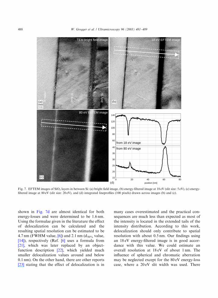
shown in Fig. 7d are almost identical for bothenergy-losses and were determined to be 1.6 nm.Using the formulae given in the literature the effectof delocalization can be calculated and theresulting spatial resolution can be estimated to be4.7 nm (FWHM value, [6]) and 2.1 nm (d50% value,[14]), respectively (Ref. [6] uses a formula from[21], which was later replaced by an object-function description [22], which yielded muchsmaller delocalization values around and below0.1 nm). On the other hand, there are other reports[23] stating that the effect of delocalization is in
many cases overestimated and the practical con-sequences are much less than expected as most ofthe intensity is located in the extended tails of theintensity distribution. According to this work,delocalization should only contribute to spatialresolution with about 0.5 nm. Our findings usingan 18 eV energy-filtered image is in good accor-dance with this value. We could estimate anoverall resolution at 18 eV of about 1 nm. Theinfluence of spherical and chromatic aberrationmay be neglected except for the 80 eV energy-losscase, where a 20 eV slit width was used. There
ARTICLE IN PRESS
5 nm
TEM bright field image
40
35
30
25
20
15806040200
position [nm]
from 80 eV image
140
120
100
80
60from 18 eV image
18 eV EFTEM image
80 eV EFTEM image
Si w
afer
poly
Si
poly
Si
SiO
2
SiO
2
(a) (b)
(c)
(d)
Fig. 7. EFTEM images of SiO2 layers in between Si: (a) bright field image, (b) energy-filtered image at 18 eV (slit size: 5 eV), (c) energy-
filtered image at 80 eV (slit size: 20 eV), and (d) integrated lineprofiles (100 pixels) drawn across images (b) and (c).
W. Grogger et al. / Ultramicroscopy 96 (2003) 481–489488
chromatic aberration is estimated to contributebetween 5% and 10% to the total resolution value.
5. Conclusions
In this work, the terms ‘‘spatial resolution’’ and‘‘detection limit’’ were described with respect totheir relation to EFTEM. Length measurementson a nm or sub-nm length scale depend on spatialresolution, therefore, a knowledge of the value ofspatial resolution is required to accurately deter-mine the dimensions of the features analyzed.The EFTEM investigation of a Mn/PdMn
multilayer specimen demonstrates the relationshipbetween ‘‘real’’ and ‘‘apparent’’ dimensions andtheir dependency on spatial resolution. Further-more, these relationships also allow to give anestimate for the detection limit (in terms ofminimum layer thickness in this particular appli-cation example).Using a SiO2 multilayer specimen, the effect of
delocalization was shown to have much influenceon spatial resolution of low-loss EFTEM images.Even at an energy-loss of 18 eV a spatial resolutionof 1 nm is possible.
Acknowledgements
Werner Grogger acknowledges support fromthe Max Kade Foundation for his stay in Berkeley.Work at LBNL/NCEM was supported by the USDepartment of Energy (contract No. DE-AC03-76SF00098). Work at FELMI was financiallysupported by the Forschungsf .orderungsfonds f .urdie gewerbliche Wirtschaft, Vienna, Austria.Dr. Jae-Pyoung Ahn and Dr. Gerald Meinhardt,austriamicrosystems, Unterpremst.atten, Austria,are gratefully acknowledged for making theMn/PdMn and the Si oxide test specimens,respectively.
References
[1] B. Freitag, W. Mader, J. Microsc. 194 (1999) 42.
[2] K.T. Moore, J.M. Howe, D.R. Veblen, Phil. Mag. B 82
(2002) 13.
[3] F. Hofer, P. Warbichler, W. Grogger, Ultramicroscopy 59
(1995) 15.
[4] J. Mayer, D.V. Szabo, M. R .uhle, M. Seher, R. Riedel,
J. Eur. Ceram. Soc. 15 (1995) 717.
[5] L. Coast-Smith, R. Brydson, P. Tsakiropulos, F. Hofer,
W. Grogger, D.V. Dunford, C.M. Ward-Close, Micron 29
(1998) 17.
[6] O.L. Krivanek, M.K. Kundman, K. Kimoto, J. Microsc.
180 (1995) 277.
[7] F. Hofer, P. Warbichler, W. Grogger, O. Lang, Micron 26
(1995) 377.
[8] R. Brydson, F. Hofer, D. Upadhyaya, G. Kothleitner, M.
Ward-Close, P. Tsakiropoulos, S. Froess, Micron 27
(1996) 107.
[9] W. Grogger, K.M. Krishnan, R.A. Ristau, T. Thomson,
S.D. Harkness, R. Ranjan, Appl. Phys. Lett. 80 (2002)
1165.
[10] M. Varela, W. Grogger, D. Arias, Z. Sefrioui, C. Leon, C.
Ballesteros, K.M. Krishnan, J. Santamaria, Phys. Rev.
Lett. 86 (2001) 5156.
[11] H. Kurata, S. Moriguchi, S. Isoda, T. Kobashi, J. Electron
Microsc. 45 (1996) 79.
[12] H. Hashimoto, Z.P. Luo, M. Kawasaki, F. Hosokawa, E.
Sukedai, Proceedings of the Institute of Physics Elec-
tron Microscopy and Analysis Group Conference, 1997,
p. 155.
[13] O. Eibl, Ultramicroscopy 69 (1997) 289.
[14] R.F. Egerton, J. Electron Microsc. 48 (1999) 711.
[15] T. Navidi-Kasmai, H. Kohl, Ultramicroscopy 81 (2000)
223.
[16] H. Kohl, A. Berger, Ultramicroscopy 59 (1995) 191.
[17] C. Jeanguillaume, P. Trebbia, C. Colliex, Ultramicroscopy
3 (1987) 237.
[18] F. Hofer, P. Warbichler, W. Grogger, Ultramicroscopy 59
(1995) 15.
[19] H.A. Liebhafsky, H.G. Pfeiffer, E.H. Winslow, P.D.
Zemany, X-Rays, Electrons and Analytical Chemistry,
Wiley, New York, 1972, p. 349.
[20] B. Schaffer, Dipl. Thesis, Graz University of Technology,
2002.
[21] S.J. Pennycok, Contemp. Phys. 23 (1982) 371.
[22] S.J. Pennycook, D.E. Jesson, A.J. McGibbon, P.D. Nellist,
J. Electron Microsc. 45 (1996) 36.
[23] D.A. Muller, J. Silcox, Ultramicroscopy 59 (1995) 195.
ARTICLE IN PRESS
W. Grogger et al. / Ultramicroscopy 96 (2003) 481–489 489
Related Documents