93 4 The Exploitation of the Spin-Transfer Torque Effect for CMOS Compatible Beyond Von Neumann Computing Thomas Windbacher, Alexander Makarov, Siegfried Selberherr, Hiwa Mahmoudi, B. Gunnar Malm, Mattias Ekström, and Mikael Östling CONTENTS 4.1 Introduction .......................................................................................................................... 95 4.2 Fundamentals of Spintronics ............................................................................................. 97 4.2.1 Magnetoresistance ................................................................................................... 97 4.2.1.1 Giant Magnetoresistance ......................................................................... 97 4.2.1.2 Tunnel Magnetoresistance ....................................................................... 99 4.2.2 Spin-Transfer Torque ............................................................................................. 100 4.2.3 Spin Hall/Spin-Orbit Effect.................................................................................. 102 4.2.4 Magnetoelectric Effect........................................................................................... 103 4.3 Materials and Their Processing ....................................................................................... 103 4.3.1 Back End of Line Integration................................................................................ 104 4.3.1.1 MRAM Cell Density ............................................................................... 104 4.3.1.2 MTJ Multilayer Stack Deposition ......................................................... 105 4.3.1.3 Two-Dimensional Materials in the MTJ Stack .................................... 106 4.3.1.4 MTJ Shape, Patterning, and Etching .................................................... 106 4.3.1.5 Nonvolatile Logic .................................................................................... 106 4.3.1.6 Access to Foundry Process Flow .......................................................... 107 4.3.2 Reliability and Yield Issues .................................................................................. 107 4.3.2.1 Time Dependent Dielectric Breakdown .............................................. 107 4.3.2.2 Electromigration and Self-Heating....................................................... 107 4.3.2.3 Shorting of the Tunnel Junction and Etch Damage ........................... 107 4.3.2.4 Voids/Open Failures............................................................................... 108 4.3.2.5 Disturbance by Internal and External Fields ...................................... 108 4.4 Spintronic Memory ............................................................................................................ 109 4.4.1 Magnetic Layer Design ......................................................................................... 110 4.4.1.1 Free and Reference Layer ....................................................................... 110 4.4.1.2 MTJ Properties......................................................................................... 113 4.4.2 Magnetic Random Access Memory .................................................................... 118 4.4.2.1 Thermally-Assisted MRAM .................................................................. 118 4.4.2.2 Spin-Transfer Torque MRAM ................................................................ 118 4.4.2.3 Spin-Hall/Spin-Orbit MRAM ............................................................... 118 4.4.2.4 Domain Wall MRAM ............................................................................. 119 4.4.2.5 Voltage Controlled Magnetic Anisotropy MRAM ............................. 120 4.4.3 Memory Cell Architecture ................................................................................... 120

Welcome message from author
This document is posted to help you gain knowledge. Please leave a comment to let me know what you think about it! Share it to your friends and learn new things together.
Transcript
93
4The Exploitation of the Spin-Transfer Torque Effect for CMOS Compatible Beyond Von Neumann Computing
Thomas Windbacher, Alexander Makarov, Siegfried Selberherr, Hiwa Mahmoudi, B. Gunnar Malm, Mattias Ekström, and Mikael Östling
CONTENTS
4.1 Introduction .......................................................................................................................... 954.2 Fundamentals of Spintronics ............................................................................................. 97
4.2.1 Magnetoresistance ................................................................................................... 974.2.1.1 Giant Magnetoresistance ......................................................................... 974.2.1.2 Tunnel Magnetoresistance .......................................................................99
4.2.2 Spin-Transfer Torque ............................................................................................. 1004.2.3 Spin Hall/Spin-Orbit Effect .................................................................................. 1024.2.4 Magnetoelectric Effect ........................................................................................... 103
4.3 Materials and Their Processing ....................................................................................... 1034.3.1 Back End of Line Integration ................................................................................ 104
4.3.1.1 MRAM Cell Density ............................................................................... 1044.3.1.2 MTJ Multilayer Stack Deposition ......................................................... 1054.3.1.3 Two-Dimensional Materials in the MTJ Stack .................................... 1064.3.1.4 MTJ Shape, Patterning, and Etching .................................................... 1064.3.1.5 Nonvolatile Logic .................................................................................... 1064.3.1.6 Access to Foundry Process Flow .......................................................... 107
4.3.2 Reliability and Yield Issues .................................................................................. 1074.3.2.1 Time Dependent Dielectric Breakdown .............................................. 1074.3.2.2 Electromigration and Self-Heating ....................................................... 1074.3.2.3 Shorting of the Tunnel Junction and Etch Damage ........................... 1074.3.2.4 Voids/Open Failures ............................................................................... 1084.3.2.5 Disturbance by Internal and External Fields ...................................... 108
4.4 Spintronic Memory ............................................................................................................ 1094.4.1 Magnetic Layer Design ......................................................................................... 110
4.4.1.1 Free and Reference Layer ....................................................................... 1104.4.1.2 MTJ Properties ......................................................................................... 113
4.4.2 Magnetic Random Access Memory .................................................................... 1184.4.2.1 Thermally-Assisted MRAM .................................................................. 1184.4.2.2 Spin-Transfer Torque MRAM ................................................................ 1184.4.2.3 Spin-Hall/Spin-Orbit MRAM ............................................................... 1184.4.2.4 Domain Wall MRAM ............................................................................. 1194.4.2.5 Voltage Controlled Magnetic Anisotropy MRAM ............................. 120
4.4.3 Memory Cell Architecture ................................................................................... 120

94 Energy Efficient Computing & Electronics
The exponential growth in (affordable) computational power over the last decades was only sustainable due to continuous successful scaling of CMOS devices. The shrinking of the CMOS transistors allowed not only an increase in the speed and performance of circuits, but also ensured that the costs per transistor dropped for every technology gen-eration. However, with each technology generation, new and ever harder to resolve obsta-cles appeared. Currently, out of the multitude of potential showstoppers in charge-based CMOS technology, the dissipated power and the energy associated with the transport of information are major concerns. The fast evolving �eld of spintronics offers a potential remedy for these problems by introducing “More than Moore” devices. The quest for the future universal memory candidate not only led to spin-based magnetoresistive random-access memory (MRAM), but also culminated in the �rst off-the-shelf MRAM products. Nevertheless, the core of the MRAM, the magnetic tunnel junction (MTJ), is not limited to memory applications. It can also be exploited for building logic-in-memory circuits with nonvolatile storage elements, as well as very compact on-chip oscillators with low power consumption. In general, the advent of nonvolatile elements, and especially spintronics in circuits, gives the unique opportunity to rethink how information is processed and moved. The concept of continuous information exchange between physically separated memory and processing units—also known as the Von Neumann architecture—has become a performance limiting bottleneck. The transition towards beyond Von Neumann architec-tures obviously also requires a redesign of all basic computational building blocks. In the this chapter, we will give an overview about the ideas and concepts for such beyond Von Neumann systems. First, we will present a short introduction into the physics necessary to understand the spintronic effects, like the magnetoresistance effect, spin-transfer torque (STT), spin Hall effect, and the magnetoelectric effect. Then we will move towards spin-tronic devices and circuits and their different concepts and architecture levels, where they introduce nonvolatility, such as thermally-assisted (TA)-MRAM, STT-MRAM, domain wall (DW)-MRAM, spin-orbit torque (SOT)-MRAM, spin-transfer torque and spin Hall oscilla-tors, logic-in-memory, all-spin logic, buffered magnetic logic gate grid, ternary content
4.5 Spintronic Logic ................................................................................................................. 1224.5.1 Logic-in-Memory ................................................................................................... 1234.5.2 Spin-Transfer Logic ................................................................................................ 124
4.5.2.1 Nonvolatile Magnetic Flip Flop ............................................................ 1244.5.2.2 Nonvolatile Magnetic Shift Register .................................................... 1264.5.2.3 Nonvolatile Buffered Magnetic Gate Grid .......................................... 127
4.5.3 All-Spin Logic ......................................................................................................... 1304.5.4 Domain Wall Logic ................................................................................................ 1314.5.5 Reprogrammable Logic ......................................................................................... 1324.5.6 Implication Logic ................................................................................................... 1344.5.7 Compute-in-Memory ............................................................................................. 136
4.6 Spin-Torque Oscillator ....................................................................................................... 1374.7 Applications ........................................................................................................................ 139
4.7.1 Random Number Generator................................................................................. 1394.7.2 Ternary Content-Addressable Memory .............................................................. 1394.7.3 Spin-Transfer Torque Compute-in-Memory (STT-CiM) ................................... 140
4.8 Conclusion and Outlook ................................................................................................... 140Acknowledgment ........................................................................................................................ 141References ..................................................................................................................................... 141
95The Exploitation of the Spin-Transfer Torque Effect for CMOS Compatible Computing
addressable memory (TCAM), and random number generators. From our point of view, there will be no disruptive transition from pure CMOS to pure spintronic circuits. Instead, there will be a gradual introduction and substitution of existing CMOS devices by spin-tronic devices, where they outperform CMOS devices in one or more aspects. Therefore, we will concentrate on and emphasize concepts and devices that are CMOS compatible and present possibilities for different levels of integration into CMOS technology.
Finally, we summarize the current state-of-the-art and extrapolate an outlook regarding future development of the �eld and prospective devices from our point of view.
4.1 Introduction
The persistence and ingenuity of scientists and engineers made it possible to maintain the miniaturization of electronic components and interconnects for many decades. This still ongoing strategy led to the current 14 nm node with multi-gate three-dimensional transistors [3] and culminated in the announcement of the mass production of 10 nm node products for 2017 [4–6]. In principle, devices with a few nanometers gate length are feasible [7], but their introduction into large scale manufacturing is rather challenging due to fabri-cation and control issues that translate into reliability problems. In conjunction with their broad variability, which manifests in high integration costs, it is clear that in the foresee-able future scaling will come to a halt.
However, looking at the very core of the MOSFET operation, the interaction between the electrons’ charge and an electric �eld, reveals that there is another intrinsic electron property, which can be harnessed as an alternative degree of freedom—the electron spin. It not only holds the potential to complement, but to substitute the currently omnipresent charge degree of freedom for future electronic devices [8,9]. The electron spin is the angu-lar momentum of the electron due to its intrinsic rotation and is commonly measured by its projection along a given axis. The introduction of the axis results in two possible projec-tions (parallel and antiparallel to the axis), which can be facilitated for digital information processing. A further advantage of exploiting spin as a degree of freedom is the very small amount of energy, which is required to invert its orientation. All spin-based technolo-gies share advantageous features like a low supply voltage, small device count, and zero static power [10]. An essential aspect for the realization of all-spin-based computing is the understanding and control of the injection, propagation, and detection of spin signals, which has been achieved only recently. The dif�culties to demonstrate spin injection from a ferromagnetic layer into a semiconductor origin from the inherent spin impedance mis-match between these materials [11]. This problem can be solved by the introduction of a potential barrier between the metal and the semiconductor [12]. Another obstacle on the way towards all-spin computation is the growth of contacts with low resistivity per area for good spin injection. In [13], it has been shown that spin injection through single layer graphene contacts are a promising close to optimal solution [14].
One of the major differences between spin and charge injected into a semiconductor is that the spin signal is not conserved. During the diffusion of the spin information carrying electrons, their net spin relaxes through scattering events to the equilibrium value of non-magnetic semiconductors—zero. Even though Huang et al. [15] successfully demonstrated spin injection and propagation over 350 μm through a silicon wafer at 77 K, the diffusion length is reduced to approximately 200 nm at room temperature [14].
96 Energy Efficient Computing & Electronics
Unfortunately, this length reduces even further in CMOS technology mainly due to the increased number of scattering events at the interfaces [16]. However, there is a trick to boost the spin lifetime in such systems. In (001) silicon �lms, the governing scattering mechanism that reduces the spin lifetime is the intervalley scattering between equivalent valleys. If one introduces uniaxial stress along the (110) direction, the degeneracy is lifted and the respective intervalley scattering is signi�cantly reduced, which leads to a large increase in the spin lifetime [17,18]. Strain has been used for many years in the semiconduc-tor industry to boost the electron mobility; thus, it is easy to exploit the same well estab-lished methods for enhancing the spin lifetime.
Furthermore, it has been shown that purely electrical spin manipulation in InGaAs het-erostructures with point contacts is possible at low temperatures [19]. The down side of this is the very poor control of the spin signal by voltage-dependent spin-orbit interaction in silicon channels. Therefore, the only feasible way to introduce spin into nano-scale CMOS technology is to add ferromagnetic source and drain contacts [20]. Such structures exhibit different currents depending on the relative orientation of the magnetization orientation of source and drain, which can be exploited for the realization of reprogrammable non-volatile logic. However, this is quite unsatisfying due to the rather low magnetoresistance ratios in comparison to MTJs. Therefore, the most promising way for the introduction of practical spin-driven applications within the next few years will likely be an MTJ-based solution.
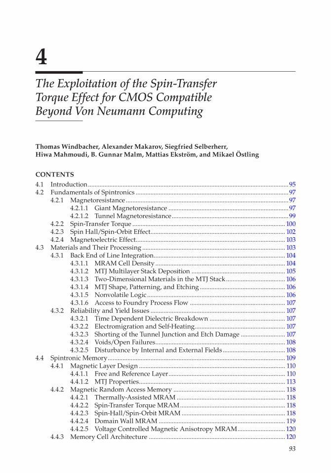
An MTJ comprises two magnetic layers that sandwich a nonmagnetic thin insulating layer (cf. Figure 4.1). Depending on the relative orientation between the magnetizations of the two magnetic layers, MTJs either exhibit a low resistance state (LRS, parallel) or a high resistance state (HRS, antiparallel). The two resistance states LRS and HRS are assigned to logic “0” and “1,” respectively [21,22].
FIGURE 4.1An MTJ consists of two magnetic layers separated by a nonmagnetic insulating layer. Depending on the mag-netization orientation of the free and the reference magnetic layer with respect to each other, the electrons traversing through the layer stack experience more (antiparallel) or less (parallel) scattering, which is re�ected in a high (HRS) and a low resistance state (LRS), respectively.
97The Exploitation of the Spin-Transfer Torque Effect for CMOS Compatible Computing
A universal memory that squares the circle of simultaneously being fast, nonvolatile, small in size, allows high integration density, and is CMOS compatible is spin-transfer-torque-based MRAM, one of the most promising candidates so far [22–25].
But the emerging spin-based technology has much more to offer. For instance, it can be used to build very compact versatile on-chip oscillators with low power consumption for consumer electronics and telecommunication applications. MRAM is also exploitable for logic-in-memory architectures, where the memory elements sit on top of the CMOS logic circuits. The combination of the nonvolatility of the memory elements and the considerably shorter interconnects guarantee low power losses and fast operation. There are already spin-based solutions able to compete with pure CMOS with respect to energy consumption and speed; however, one of the key aspects to be competitive in the market—the integration density—is still worse than in pure CMOS. Therefore, we will also look into ideas and technologies that have the potential for high integration density.
In the following section, we will �rst give an overview about the physical fundamentals of spintronics to allow the reader to concentrate on the devices and circuits in later sections. Since the peculiarities of the employed materials and their processing are essential to understand the current limitations for designing and manufacturing spintronic devices, the subsequent section is dedicated to these aspects. Then the different types of spintronic memory will be elucidated, followed by a spintronic logic section where different possibilities to implement logic will be explained. Afterwards the applications section will highlight some spintronic solutions to demonstrate the potential of spintronics in future applications. Finally, we will conclude the chapter and try to extrapolate how spintronics will develop in the future.
4.2 Fundamentals of Spintronics
In order to enable the reader to concentrate on the spintronic devices and circuits without the need to take breaks to look up physics details, a short section that will help to grasp the most relevant basic physical effects is provided here.
4.2.1 Magnetoresistance
The discovery of �rst the giant magnetoresistance (GMR) and later the tunneling magne-toresistance (TMR) were essential for the development of widely usable spintronic devices.
4.2.1.1 Giant Magnetoresistance
The GMR has been observed for the �rst time in Fe/Cr superlattices in the late 1980s by two independent researchers Baibich et al. [26] and Binasch et al. [27].
The GMR effect is observed when a current is passed through a stack of two or more magnetic layers that are separated by nonmagnetic conducting spacer layers. The mea-sured resistance depends on the magnetization orientation of the magnetic layers with respect to each other. Commonly the strength of the GMR effect is expressed as the ratio between the high and low resistance states [28]:
GMRR R
RAP P
P
AP P
P
P
AP= = = 1
− − −ρ ρρ
σσ
(4.1)
98 Energy Efficient Computing & Electronics
RAP (high resistance) and RP (low resistance) denote the resistances for antiparallel and par-allel layer magnetization orientations, ρAP and ρP are the associated resistivities, and σ AP and σ P the corresponding conductivities, respectively.
According to the de�nition in Equation 4.1 the GMR can become larger than 1, if ρ ρAP P> . To avoid confusion, there is also an alternative de�nition where the GMR is never larger than 1 (ρ ρAP P> ) [28]:
GMR AP P
AP
AP
P
′ − −= = 1ρ ρ
ρσσ
(4.2)
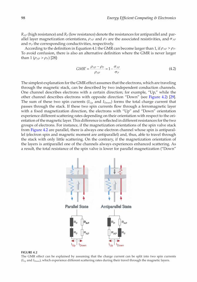
The simplest explanation for the GMR effect assumes that the electrons, which are traveling through the magnetic stack, can be described by two independent conduction channels. One channel describes electrons with a certain direction; for example, “Up,” while the other channel describes electrons with opposite direction “Down” (see Figure 4.2) [29]. The sum of these two spin currents (IUp and IDown) forms the total charge current that passes through the stack. If these two spin currents �ow through a ferromagnetic layer with a �xed magnetization direction, the electrons with “Up” and “Down” orientation experience different scattering rates depending on their orientation with respect to the ori-entation of the magnetic layer. This difference is re�ected in different resistances for the two groups of electrons. For instance, if the magnetization orientations of the spin valve stack from Figure 4.2 are parallel, there is always one electron channel whose spin is antiparal-lel (electron spin and magnetic moment are antiparallel) and, thus, able to travel through the stack with only little scattering. On the contrary, if the magnetization orientation of the layers is antiparallel one of the channels always experiences enhanced scattering. As a result, the total resistance of the spin valve is lower for parallel magnetization (“Down”
RP
RP RAPR
RRAPAPRR RP RAPR
RPRAPR
IUp IDown IUp IDown
FIGURE 4.2The GMR effect can be explained by assuming that the charge current can be split into two spin currents (IUp and IDown), which experience different scattering rates during their travel through the magnetic layers.

99The Exploitation of the Spin-Transfer Torque Effect for CMOS Compatible Computing
channel experiences only little scattering) than for antiparallel (both “Up” and “Down” channels exhibit a zone with increased scattering) [30].
This effect opened up the path for the development of today’s hard disk drive read heads and encouraged research in GMR-based MRAM [31].
4.2.1.2 Tunnel Magnetoresistance
Another important effect that has great signi�cance in current MRAM applications is the TMR. It was discovered by Julliere et al. [32] in a Fe/Ge/Co junction at temperatures below 4.2K in 1975. Similar to the GMR effect, TMR can be observed, where two magnetic layers sandwich a nonmagnetic insulating layer and the measured resistance depends on the magnetization orientation of the two magnetic layers with respect to each other. However, in this case the separating nonmagnetic layer is a thin metal-oxide (e.g., Al2O3 or MgO) and forms a MTJ in contrast to the GMR, where the nonmagnetic layer is composed of a metal (e.g., Cu) and forms a spin valve.
The TMR effect is quanti�ed as the relative ratio between the parallel and antiparallel resistance states of the stack [33,34]:
TMRR R
RAP P
P=
− (4.3)
Analog to before, RAP and RP denote the high (antiparallel) and low (parallel) resistance states of the stack.
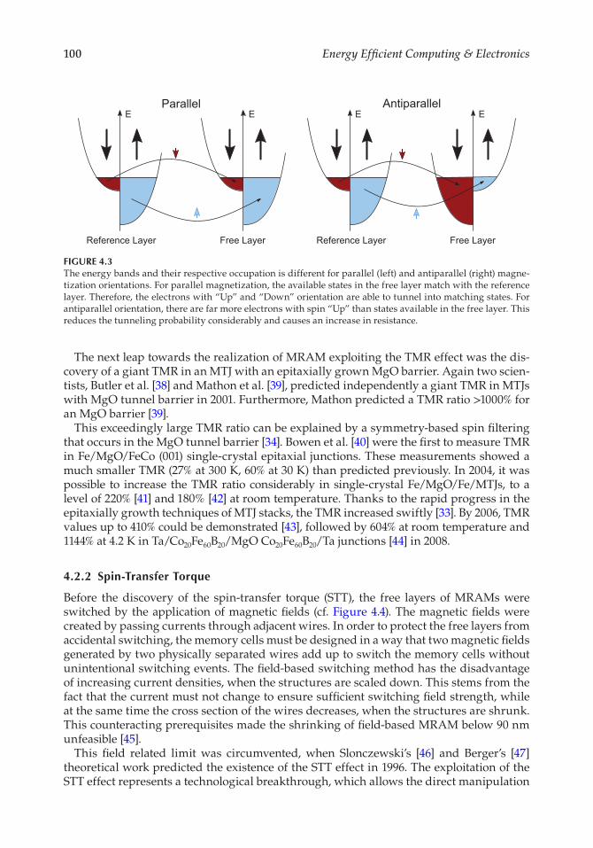
The source of this effect can be attributed to the difference in tunneling probabilities for the electrons with certain orientation (e.g., “Up” or “Down”) from one ferromagnetic layer (reference layer) to the other ferromagnetic layer (free layer) through the oxide for a given magnetization state. Figure 4.3 depicts the energy bands and their respective occupation for the parallel (left) and the antiparallel (right) magnetization state. If the magnetizations of both layers are parallel (e.g., both point “Up”), the majority of the electrons occupies “Up” states and the minority “Down” states in the reference layer as well as in the free layer. Therefore, the bands and their occupation match, which makes it easier for the electrons to tunnel through the thin nonconducting layer. This state has a higher conductance (lower resistivity). In the case of antiparallel magnetization orienta-tions (e.g., reference layer→“Up” and free layer→“Down”), the majority of the electrons in the free layer are in “Down” states and the minority of the electrons in “Up” states. Therefore, there are far more electrons in the reference layer with “Up” than matching states available in the free layer, which leads to a strongly reduced tunneling probability. Even though the spin “Down” electrons from the reference layer �nd plenty of available states in the reference layer, their total number is much smaller than the amount of “Up” electrons. Thus, they can only contribute little to the total conductance of the stack. In summary, the overall conductance is strongly decreased and an increase in the stack resistance is observed.
Although the TMR effect was found earlier than the GMR effect, its practical use was limited due to poor TMR values, until the advent of stacks with amorphous Al2O3 as tun-nel barrier. Moodera et al. [35] and Miyazaki et al. [36] where the �rst who developed independently such structures. The largest TMR ratio for an MTJ with amorphous Al2O3 tunnel barrier at room temperature so far was demonstrated by Wang et al. [37] in 2004 and amounts to 70.4%.
100 Energy Efficient Computing & Electronics
The next leap towards the realization of MRAM exploiting the TMR effect was the dis-covery of a giant TMR in an MTJ with an epitaxially grown MgO barrier. Again two scien-tists, Butler et al. [38] and Mathon et al. [39], predicted independently a giant TMR in MTJs with MgO tunnel barrier in 2001. Furthermore, Mathon predicted a TMR ratio >1000% for an MgO barrier [39].
This exceedingly large TMR ratio can be explained by a symmetry-based spin �ltering that occurs in the MgO tunnel barrier [34]. Bowen et al. [40] were the �rst to measure TMR in Fe/MgO/FeCo (001) single-crystal epitaxial junctions. These measurements showed a much smaller TMR (27% at 300 K, 60% at 30 K) than predicted previously. In 2004, it was possible to increase the TMR ratio considerably in single-crystal Fe/MgO/Fe/MTJs, to a level of 220% [41] and 180% [42] at room temperature. Thanks to the rapid progress in the epitaxially growth techniques of MTJ stacks, the TMR increased swiftly [33]. By 2006, TMR values up to 410% could be demonstrated [43], followed by 604% at room temperature and 1144% at 4.2 K in Ta/Co20Fe60B20/MgO Co20Fe60B20/Ta junctions [44] in 2008.
4.2.2 Spin-Transfer Torque
Before the discovery of the spin-transfer torque (STT), the free layers of MRAMs were switched by the application of magnetic �elds (cf. Figure 4.4). The magnetic �elds were created by passing currents through adjacent wires. In order to protect the free layers from accidental switching, the memory cells must be designed in a way that two magnetic �elds generated by two physically separated wires add up to switch the memory cells without unintentional switching events. The �eld-based switching method has the disadvantage of increasing current densities, when the structures are scaled down. This stems from the fact that the current must not change to ensure suf�cient switching �eld strength, while at the same time the cross section of the wires decreases, when the structures are shrunk. This counteracting prerequisites made the shrinking of �eld-based MRAM below 90 nm unfeasible [45].
This �eld related limit was circumvented, when Slonczewski’s [46] and Berger’s [47] theoretical work predicted the existence of the STT effect in 1996. The exploitation of the STT effect represents a technological breakthrough, which allows the direct manipulation
E E
Reference Layer Free Layer
ParallelE E
Reference Layer Free Layer
Antiparallel
FIGURE 4.3The energy bands and their respective occupation is different for parallel (left) and antiparallel (right) magne-tization orientations. For parallel magnetization, the available states in the free layer match with the reference layer. Therefore, the electrons with “Up” and “Down” orientation are able to tunnel into matching states. For antiparallel orientation, there are far more electrons with spin “Up” than states available in the free layer. This reduces the tunneling probability considerably and causes an increase in resistance.
101The Exploitation of the Spin-Transfer Torque Effect for CMOS Compatible Computing
of the magnetization of a layer through a spin polarized current and renders the previ-ously employed indirect switching via Ørsted �elds super�uous.
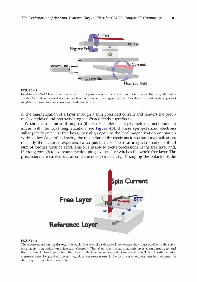
When electrons move through a (thick) �xed reference layer, their magnetic moment aligns with the local magnetization (see Figure 4.5). If these spin-polarized electrons subsequently enter the free layer, they align again to the local magnetization orientation within a few Ångström. During the relaxation of the electrons to the local magnetization, not only the electrons experience a torque, but also the local magnetic moments (total sum of torques must be zero). This STT is able to excite precessions in the free layer and, if strong enough to overcome the damping, eventually switches the whole free layer. The precessions are carried out around the effective �eld Heff. Changing the polarity of the
FIGURE 4.5The electrons traversing through the stack, �rst pass the reference layer, where they align parallel to the refer-ence layers’ magnetization orientation (bottom). Then they pass the nonmagnetic layer (transparent gap) and �nally enter the free layer, where they relax to the free layers magnetization orientation. This relaxation creates a spin-transfer torque that drives magnetization precessions. If the torque is strong enough to overcome the damping, the free layer is switched.
FIGURE 4.4Field-based MRAM requires two wires for the generation of the writing �eld. Only when the magnetic �elds created by both wires add up, the free layer will switch its magnetization. This design is deliberate to protect neighboring memory cells from accidental switching.
102 Energy Efficient Computing & Electronics
applied current �ips the orientation of the exerted STT and, thus, allows to repeatably switch the free layer between antiparallel and parallel orientation with respect to the refer-ence layer (see Figure 4.6).
Nevertheless, it took years until STT-induced switching could be demonstrated experi-mentally on all-metallic stacks [45]. Co/Cu/Co was the �rst GMR-based stack to proof the concept of STT-induced switching [48–52]. The �rst working STT-switched MTJ memory cells based on AlOx were shown in 2004 [53] and based on MgO in 2005 [54].
4.2.3 Spin Hall/Spin-Orbit Effect
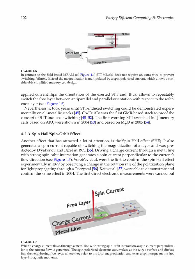
Another effect that has attracted a lot of attention, is the Spin Hall effect (SHE). It also generates a spin current capable of switching the magnetization of a layer and was pre-dictedby D’yakonov and Perel in 1971 [55]. Driving a charge current through a metal line with strong spin orbit interaction generates a spin current perpendicular to the current’s �ow direction (see Figure 4.7). Vorob’ev et al. were the �rst to con�rm the spin Hall effect experimentally in 1979 by observing a change in the rotation rate of the polarization plane for light propagating through a Te crystal [56]. Kato et al. [57] were able to demonstrate and con�rm the same effect in 2004. The �rst direct electronic measurements were carried out
FIGURE 4.7When a charge current �ows through a metal line with strong spin-orbit interaction, a spin current perpendicu-lar to the current �ow is generated. The spin polarized electrons accumulate at the wire’s surface and diffuse into the neighboring free layer, where they relax to the local magnetization and exert a spin torque on the free layer’s magnetic moments.
FIGURE 4.6In contrast to the �eld-based MRAM (cf. Figure 4.4) STT-MRAM does not require an extra wire to prevent switching failures. Instead the magnetization is manipulated by a spin polarized current, which allows a con-siderably simpli�ed memory cell design.
103The Exploitation of the Spin-Transfer Torque Effect for CMOS Compatible Computing
by Valenzuela and Tinkham [58]. As it turned out later, they actually observed the inverse spin Hall effect (ISHE), since in their case they created a spin current, which generated a perpendicular charge current that accumulated at the edges of the sample exploited for electrical measurement [59]. For their work, they used a ferromagnetic electrode to gener-ate a spin current and subsequently injected it into a nonmagnetic metal strip, where they took advantage of the ISHE as well as the nonlocal spin valve effect with the aid of a fer-romagnetic probe electrode for the spin signal detection.
Further work regarding the SHE and the ISHE effect was carried out by Kimura et al. [60,61] and is based on NiFe/Cu/Pt structures. The spin current was measured by exploit-ing a nonlocal spin signal and the ISHE. Their work paved the way for the exploitation of the SHE and the ISHE as spin injection and detection tools.
4.2.4 Magnetoelectric Effect
Analog to the initially employed current controlled bipolar junction transistors, also the STT-based spintronic devices always require some kind of charge �ow and thus also exhibit Joule heating as an energy dissipation mechanism during switching. This prob-lem drove the transition from bipolar junction transistors to �rst N/P-MOS devices and eventually to the state-of-the-art CMOS technology. Therefore, ideally one could switch in spintronics from current-based to voltage-based magnetization dynamics manipulation in order to bene�t the same way from the signi�cant reduction in power dissipation [62].
Weisheit et al. [63] showed that the magnetocrystalline anisotropies of FePt and FePd compounds can be reversibly switched by an externally applied electric �eld. It was also demonstrated that a relatively small electric �eld can induce a large ∼40% change in the magnetic anisotropy of a bcc Fe(001)/MgO(001) junction [64]. Furthermore, it was demon-strated that the magnetocrystalline anisotropy of Fe80Co20(001)/MgO(001) cannot only be changed by an electric �eld, but actually voltage-assisted switched [65]. Nozaki et al. [66] showed high-frequency voltage-assisted magnetization reversal in MgO-MTJs in 2014. They could demonstrate a switching �eld reduction of >80% at a radio frequency of 3 dBm. Recently, Li et al. [67] could show that the introduction of a thin Mg layer at the CoFeB/ MgO interface causes a 3× increase in the voltage controlled anisotropy coef�cient (from commonly ∼30 fJ/Vm to ∼100 fJ/Vm). This is very encouraging, because it allows to reduce the write voltage below 0.6 V, which allows to employ advanced CMOS transistors.
The drastic change in the magnetocrystalline anisotropy strength of ultra-thin layers under the application of an electric �eld can be attributed to a change in the occupation of the atomic orbitals at the CoFeB/MgO interface, which together with the spin-orbit inter-action, alters the anisotropy [62,67,68]. However, it can be also explained by the interfacial Rashba effect [62,69].
4.3 Materials and Their Processing
Since the peculiarities of the employed materials and their processing are essential to understand the current limits for designing and manufacturing spintronic devices, this section is dedicated to these aspects. A recurring theme of discussion is the integration with advanced CMOS process nodes, since a complete MRAM cell features a controlling transistor in combination with the MTJ element. MRAM technology has a few distinct
104 Energy Efficient Computing & Electronics
reliability issues and the large interest for MRAM technology has prompted tool vendors to develop dedicated tools. Acceptance of MRAM technology is manifested by its adoption into foundry process lines.
4.3.1 Back End of Line Integration
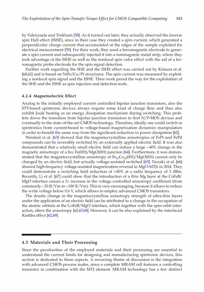
In integrated circuits the back end of line (BEOL) process refers to the fabrication of metal interconnects and the intermetal dielectrics (IMD) layers. Using successive deposition of metal (Cu), patterning of metal lines, IMD deposition, and planarization of the IMD lay-ers, more than 10 layers of interconnecting Cu-lines can be realized. This is suf�cient for the routing of signal and power supply lines in very complex circuits, with 100 millions of integrated transistors. All BEOL process steps are performed at low temperature, typically in the range 350°C–400°C. Therefore, the integration of spintronic memory and logic based on multilayer ferromagnetic metallic stacks with thin metal-oxide tunneling barriers is feasible. The MTJ stacks will not suffer from interdiffusion and the integrity of the tunnel-ing barrier can be maintained [2,44]. Speci�cally the MgO barrier must be annealed under controlled conditions to obtain a proper crystallographic reorientation epitaxially along the (001) direction. More importantly, annealing is also necessary to induce the interfa-cial perpendicular magnetic anisotropy (PMA) effect for stacks based on CoFeB, which is intrinsically an in-plane material [70]. A comprehensive review of the PMA and its applica-tions in [71]. The PMA can also be strengthened by using, for example, multilayer Co/Pt with inherent PMA or synthetic antiferromagnetic (SAF) layers in the MTJ stack [72]. Capping layers (e.g., silicon nitride) are used to protect the MTJ from unintentional reox-idation during later stages of processing. The MTJs are typically inserted close to the top metal layers. The MTJ bottom electrode is connected to an already available Cu-line in, for example, metal level 5 (M5), [1]. Subsequent MTJ layers are deposited without break-ing the vacuum, patterned by lithography and etching and then embedded in the subse-quent IMD layer. The IMD thickness depends on the layer and is chosen to minimize the interconnect capacitances. The MTJ stack total thickness is less than the IMD thickness so that the MTJ becomes fully embedded. For an illustration of production near embedded MRAM, see Figure 4.8.
To implement MTJs in the BEOL process �ow the minimum additional lithographic mask count is three or four. To put this into perspective, a 14 nm advanced CMOS process node uses close to 70 mask steps. Also for comparison it is interesting to note that embed-ded �ash nonvolatile memory has an added mask count as high as a dozen. Embedded static random-access memory (SRAM) has a signi�cantly larger footprint or cell area, while embedded dynamic random-access memory (DRAM) is a quite complex process module, including high aspect ratio etching and �lling steps for the storage capacitors.
4.3.1.1 MRAM Cell Density
The metal pitch in advanced technology nodes is compatible with the size of an MTJ ele-ment and the area of the complete MRAM cell, including one controlling CMOS transis-tor, follows the standard CMOS design rules. The width of the CMOS transistor must be chosen so that enough drive current can be supplied in order to reach the critical current density for STT switching. This has led some researchers to pursue devices that are voltage controlled (VC) MRAM and consume less current, allowing smaller transistors to be used [73]. A 4Gbit MRAM density has been demonstrated with 90 nm pitch [74]. The minimum pitch is used in the lower metal layer while the metal pitch increases for higher layers [75].
105The Exploitation of the Spin-Transfer Torque Effect for CMOS Compatible Computing
A via needs to be opened in the IMD and aligned to the MTJ top contact area. There are several methods to achieve this, including self-aligned process schemes [76]. A combina-tion of chemical mechanical polishing (CMP) and deposition of sacri�cial or etch stop layer on top of the actual MTJ are examples for such self-alignment solutions.
4.3.1.2 MTJ Multilayer Stack Deposition
Metal layers in the BEOL �ow are deposited by sputtering tools, also known as physical vapor deposition (PVD) tools. The particular requirements for MTJ stacks include the pos-sibility to deposit a large number of elements, for example, Ta, Ru, Co, Ni, Fe, Cu, Pt, B, Mg, and Al to name the most common. The tools operate under ultra-high-vacuum conditions (UHV) corresponding to 10−8 Torr or better and feature in-situ annealing capability. The UHV condition is a key requirement, for growing sub-nm atomically abrupt layers. In research, molecular beam epitaxy is sometimes used for abrupt layers, but for production purposes PVD tools are the only choice in terms of throughput, wafer scale uniformity and metal targets available. Dedicated PVD tools for MRAM fabrication are offered in multi-cathode con�guration, able to handle the large number of elements. Examples of deposition and etching tool vendors include Applied Materials, Singulus, Canon Anelva, Oxford Instruments, and LAM. It should be noted that several of these companies already have a strong presence in microelectronics fabrication.
FIGURE 4.8Example of production-near embedded MRAM [1]. Left panel showing schematic vertical structure of 8 Mb STT-MRAM cell array embedded in 28 nm logic process. Right panel showing transmission electron micros-copy (TEM) picture of MTJ module inserted between Cu BEOL lines.
106 Energy Efficient Computing & Electronics
4.3.1.3 Two-Dimensional Materials in the MTJ Stack
Using emerging two-dimensional (2D) materials either graphene, boron-nitride (BN), MoS2, or WS2 offers an interesting path to improve the MTJ stack [77]. There have been successful demonstrations of using graphene as a tunneling barrier [78]. However, in this case the TMR is too low to consider applications. On the other hand, graphene and other monolayer materials are excellent diffusion barriers and can be used in combination with oxide tunneling barriers, since they alleviate interdiffusion issues during high tempera-ture process steps [79].
4.3.1.4 MTJ Shape, Patterning, and Etching
MTJs are patterned and etched into pillars with their material stack sandwiched in between nonmagnetic top and bottom metal contacts. First and second generation MRAM cells relied on in-plane magnetization and shape anisotropy to stabilize the magnetization of the �xed or reference layer. Therefore, elliptic shapes were mandatory. This requirement put very stringent boundaries on the pattering process since variability in shape could be detrimental to the switching energy barrier. Basically, elliptic shapes are not optimal from a patterning perspective. In standard CMOS foundry design rules, circular contacts are patterned at minimum lithographic dimensions. In current generation MRAM, the use of materials with perpendicular anisotropy removed this constraint of having elliptically shaped MTJ elements and hence signi�cantly eased the process integration. As discussed above, the MTJs are comparable to the pitches used in the BEOL and deep-UV optical lithography provides the necessary resolution and alignment. It should be mentioned that the scienti�c community relies almost exclusively on electron beam lithography, which has nanometer resolution but suffers from long writing times, and is impractical to use for alignment of multiple layers with critical dimensions.
Regardless of the patterning technique, the etching of MTJ stacks is known to be chal-lenging, because the etching residues are not very volatile. This becomes an issue in reac-tive ion etching (RIE), where the substrate temperature must be raised to achieve enough etching rate for the removal of residues and to avoid redeposition. The temperature the metal stack can tolerate is limited, so other solutions must be considered. The main tech-nique is physical etching by sputtering with low energy Ar ion beams. For this technique, there are also redeposition issues. Furthermore, since the etch is typically performed at glancing angles, the area of the patterned element will be reduced by lateral etching of the pillar sidewalls [80]. It could be advantageous to shrink the lithographic pattern size [81], but it is generally considered as a drawback of these etching tools. Many ion beam tools are equipped with in-situ analysis capabilities of the etching residues, which is highly useful for controlled etching of monolayers. Alternative methods include atomic layer deposition (ALD)/atomic layer etching (ALE), where the volatility of the etching residues is increased by controlled deposition of selected elements on the metallic surfaces [82]. For etching of multilayer stacks, the chemical reactions provide a degree of selectivity to the different materials being etched. In contrast, ion beam etching has virtually no selectivity due to its purely physical nature of material removal.
4.3.1.5 Nonvolatile Logic
Processing of nonvolatile logic based on MRAM cells is a straightforward adaption of the standard MRAM blocks (also known as macros). While these highly regular mem-ory matrices are based on a 1T/1MTJ con�guration, the relative number of transistors as
107The Exploitation of the Spin-Transfer Torque Effect for CMOS Compatible Computing
compared to MTJs increases in the hybrid realization of nonvolatile logic [83]. As an exam-ple, one would use at least six transistors and two MTJs in a �ip-�op. To reduce this area and computational energy overhead, it would be preferable to move all computation to the spin domain and to use electronics only for interfacing purposes (see Section 4.5).
4.3.1.6 Access to Foundry Process Flow
All main foundry-based actors in the semiconductor business, such as TSMC, UMC, Global Foundries, and Samsung, have announced embedded MRAM (eMRAM) options by end of 2017 (see [84]). The intellectual property (IP) needed to get started in the MRAM �eld has been transferred to the foundry partners from start up companies, closely connected to academia. Some companies have entered manufacturing agreements and continue to develop their own IP. Finally, there are some companies with strong in-house activities, notably Toshiba.
4.3.2 Reliability and Yield Issues
During quali�cation, all memory devices are subjected to thorough cycling at various operating conditions, including elevated temperatures and increased humidity. Typical speci�cations require that a nonvolatile cell retains its state over a speci�ed time (10 years) [84] and that a cell can be cycled (107 times) without any penalty in read or write voltage margin [85]. In fact, current MRAM offering surpass this signi�cantly. In particular, the number of cycles is often given as close to unlimited [86].
4.3.2.1 Time Dependent Dielectric Breakdown
For MTJs one can identify several reliability issues. The main one is the relatively high current density passing through the MgO tunneling barrier during switching. This might lead to time dependent dielectric breakdown (TDDB), which is a well known issue in advanced CMOS with thin gate oxides. The TDDB is strongly affected by the temperature, as discussed further below.
4.3.2.2 Electromigration and Self-Heating
The relatively high critical current densities posed a serious threat due to possible electro-migration in early generation spintronic devices [87]. For MTJ devices based on STT, the current densities are orders of magnitude lower. Since MTJs are embedded in isolating material with relatively low thermal conductance, there might be a signi�cant temperature increase during switching. Increased temperature is known to accelerate electromigration by a power law [88].
4.3.2.3 Shorting of the Tunnel Junction and Etch Damage
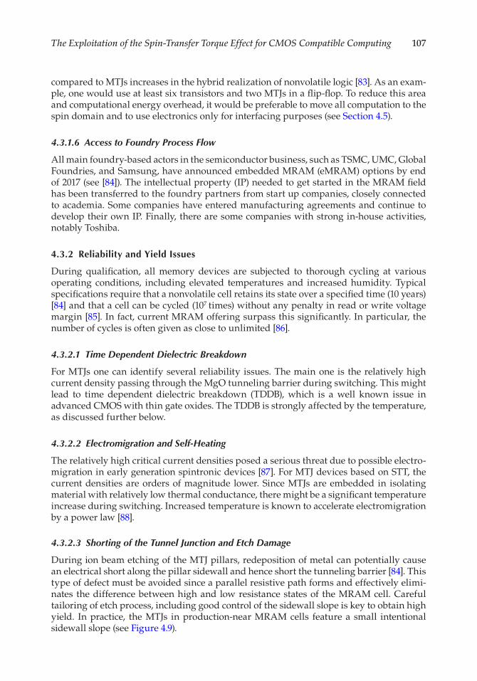
During ion beam etching of the MTJ pillars, redeposition of metal can potentially cause an electrical short along the pillar sidewall and hence short the tunneling barrier [84]. This type of defect must be avoided since a parallel resistive path forms and effectively elimi-nates the difference between high and low resistance states of the MRAM cell. Careful tailoring of etch process, including good control of the sidewall slope is key to obtain high yield. In practice, the MTJs in production-near MRAM cells feature a small intentional sidewall slope (see Figure 4.9).
108 Energy Efficient Computing & Electronics
Vertical sidewalls cannot be controlled with suf�cient accuracy in wafer scale produc-tion. In case of RIE tools, redeposition on the MTJ sidewalls also occurs, but in this case of polymer residues. These can be removed by proper post-etch cleaning steps. The chemical species used in RIE tools are very corrosive and could damage the sensitive MgO tunnel-ing barrier. Again, post process cleaning is essential to hinder any further corrosion due to remaining etchant species.
4.3.2.4 Voids/Open Failures
The MTJs are sputter deposited on bottom electrodes, which are part of the standard BEOL process �ow. As in any contact opening the surface should be free of residues of such polymers, which remain from previous process steps [84]. Good via �lling is essential par-ticularly for the top contact, so that all of the MTJ area is contacted. Having a partial void at either the bottom or top contact will degrade the relative changes in resistance during switching and increase the absolute value of the MTJ resistance, so that the voltage drop becomes too high.
4.3.2.5 Disturbance by Internal and External Fields
Both read and write operations of MRAM can be disturbed by external �elds. As the �rst generation MRAM cells were �eld-switched, current generations rely on spin transfer torque or voltage controlled anisotropy (cf. Sections 4.2.2 and 4.2.4). As an example of the �eld sensitivity, data sheets for commercial products give a limit of 8000 A/m. In addi-tion, in a scenario where MRAM cells are placed at minimum design rules in advanced CMOS technology nodes, neighboring cells could affect each other due to their internal stray �elds.
FIGURE 4.9Cross-sectional transmission electron microscopy image of a fully functional device integrated on 90 nm CMOS [2]. The diameter of this device is about 50 nm.
109The Exploitation of the Spin-Transfer Torque Effect for CMOS Compatible Computing
4.4 Spintronic Memory
Memory can be distinguished into two categories: volatile and nonvolatile. The volatile memories, such as SRAM and DRAM, retain their data as long as they are supplied with power. The nonvolatile memories, such as EEPROM and Flash, retain the data when powered off.
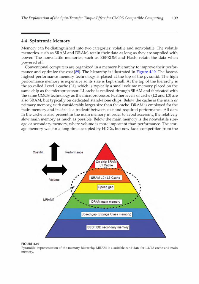
Conventional computers are organized in a memory hierarchy to improve their perfor-mance and optimize the cost [89]. The hierarchy is illustrated in Figure 4.10. The fastest, highest performance memory technology is placed at the top of the pyramid. The high performance memory is expensive so its size is kept small. At the top of the hierarchy is the so called Level 1 cache (L1), which is typically a small volume memory placed on the same chip as the microprocessor. L1 cache is realized through SRAM and fabricated with the same CMOS technology as the microprocessor. Further levels of cache (L2 and L3) are also SRAM, but typically on dedicated stand-alone chips. Below the cache is the main or primary memory, with considerably larger size than the cache. DRAM is employed for the main memory and its size is a tradeoff between cost and required performance. All data in the cache is also present in the main memory in order to avoid accessing the relatively slow main memory as much as possible. Below the main memory is the nonvolatile stor-age or secondary memory, where volume is more important than performance. The stor-age memory was for a long time occupied by HDDs, but now faces competition from the
FIGURE 4.10Pyramidal representation of the memory hierarchy. MRAM is a suitable candidate for L2/L3 cache and main memory.
110 Energy Efficient Computing & Electronics
NAND-�ash-based solid state drives (SSD). The main memory mirrors the data from the comparatively very slow storage memory in order to speed up the access times.
Currently, there are two speed-gaps in the hierarchy: Between the cache and the pri-mary memory and between the primary memory and the secondary memory [90,91]. For the gap between the primary memory and the high volume secondary memory, a new hierarchy level—the storage class memory (SCM)—has been proposed. To �ll the gap the employed memory must exhibit, a density higher than DRAM, an access time shorter than NAND-Flash, and nonvolatility. Right now there is a competition between several nonvolatile random access memory (NVRAM) types that have potential for SCM applica-tions, such as phase change memory, conductive bridge memory, resistive memory, and MRAM.
MRAM is a high performance NVRAM suitable for SCM applications, but currently not used in the SRAM, DRAM and HDD/SSD dominated memory hierarchy. MRAM has been proposed as a universal memory that can �ll all levels of the memory hierar-chy. However, the up to now rather low density prohibits any serious competition with the well established HDD/SSD technology. Due to the demand of a high density for an SCM, other NVRAMs are better suitable [90,91]. Especially, a three-dimensional mono-lithic integration of cross-bar memory arrays is more likely to succeed. These require memory cells that use a 1D-1R memory cell architecture (see Section 4.4.3). A more realistic application for MRAM is to replace SRAM and DRAM in L2/L3 cache and primary memory, respectively. It can bridge the speed gap between the cache and the primary memory. The required high endurance has been successfully demonstrated [92] and Kitagawa et al. [93] showed that a simulated mobile CPU would use less power, if it employs MRAM instead of SRAM as L2 cache. Other examples of MRAM for cache-applications can be found in [94]. MRAM is available on the market for main memory applications (DDR3 DRAM compatible) [95]. The major bene�t of replacing DRAM with a NVRAM is the removal of the refresh action, the reduction of the overall power consumption and the simpli�cation of the circuit design.
In this section, the MTJ, the core of the spintronic memory, will be discussed in depth. Its properties and trade-offs will be presented. The different varieties of spintronic mem-ories and their peculiarities will be shown and the different memory cell architectures compared.
4.4.1 Magnetic Layer Design
4.4.1.1 Free and Reference Layer
A basic MTJ is composed of three elements: The reference layer, the tunneling barrier, and the storage layer. The tunneling barrier was covered in Section 4.2.1.2.
Storage layer: The storage layer, or free layer, is the layer that stores information as magnetization direction. A necessary requirement is that the free-layer material possess an energetically favorable nonzero magnetization in the absence of an external mag-netic �eld or a remanent magnetization. There are elemental ferromagnetic materials (e.g., Fe, Co, Ni), ferrimagnetic half-metal oxides (Fe3O4, La1−xSrxMnO3), and various ferromagnetic alloys (NixFeyCoz, Heusler alloys). Today, CoFeB (Co0.20Fe0.60B0.20) is the material of choice as it has low damping [96] and provides high TMR in combination with MgO as tunneling barrier [44,97]. The free layer is a planar thin-�lm and can be further differentiated in �lms with in-plane and perpendicular magnetization direc-tion. In order to achieve a free layer with in-plane direction, the free layer commonly exhibits an elongated shape (such as elliptic or rectangular). This form creates a shape
111The Exploitation of the Spin-Transfer Torque Effect for CMOS Compatible Computing
anisotropy with two well-de�ned stable magnetization states along the major axis. The effective anisotropy �eld Hk for in-plane design is given by [96,98]:
H M dl ww l
M dARw AR
k s FF F
F Fs F
F= 2( ) = 2( )
1× −×
×
−
(4.4)
lF and wF is the length and width of the free layer (l wF F> ), respectively. AR denotes the aspect ratio (= / > 1l wF F ), dF the layer thickness, and Ms the magnetization saturation. The largest value the effective anisotropy �eld can reach is 2( )/M d ws F F. The magnetic moment m M A ds F F= × is accessible through measurements with a vibrating sample magnetometer (VSM), and, if the area A l wF F F= × is known, M ds F can be determined (= / =m A M dF s F). A typical ferromagnet (Co, Fe, Ni) exhibits an Ms of ∼ 106 A/m. The two stable states of the magnetization are separated by an energy barrier that prevents the magnetization from freely switching the direction. The energy barrier determines the retention and switching properties, as will be discussed in Section 4.4.1.2. The general model for the energy barrier is found in [96,99]:
E M H V M d H A K Vb s k F s F k F u F= /2 = ( ) /20 0µ µ = (4.5)
µ0 describes the vacuum permeability, VF the volume of the free layer (= A dF F× ), and Ku is the magnetic anisotropy energy density. The model for the energy barrier can with the aid of Equation 4.4 be further re�ned to analyze implications for in-plane designs:
E M d H A M d w ARbs F k F
s F F=( )
2( ) ( 1)0
02µ µ∼ × − (4.6)
Assuming a constant aspect ratio, one can see from Equation 4.6 that the barrier depends quadratically on the layer thickness and linearly on the layer width.
In contrast, for the perpendicular design, the effective anisotropy �eld Hk is governed by three terms [96]:
HM
Kd
Mks
bF
s=2 2 1
20 0µ µσ+ − (4.7)
The �rst term corresponds to the perpendicular bulk anisotropy (given by Kb, J/m3), the second term to the perpendicular surface anisotropy (given by σ i, J/m2), and the third term to the demagnetization energy. The perpendicular design becomes unstable, if the demag-netization energy dominates. Ferromagnetic materials behave differently in different nonequivalent crystal directions, which manifests in the magnetocrystalline anisotropy. As an example, Co, which has hexagonal symmetry, prefers a magnetization along c-axis instead of lying in the a-plane, and has an anisotropy energy of 4.5 × 10⁵ J/m3, or 2.8 × 10⁻³ eV/nm3 [100]. The magnetocrystalline anisotropy can be used as source for bulk anisotropy. If this bulk term dominates, the anisotropy �eld is independent of the �lm thickness and the energy barrier is given as
E M d H A K M d Abs F k F
b s F F=( )
212
00
2µ µ∼ −
× (4.8)
112 Energy Efficient Computing & Electronics
In this case, the energy barrier increases with increasing volume. Both magnetocrystalline anisotropy and damping are correlated functions of spin-orbit coupling [100,101]; thus, systems using intentionally high magnetocrystalline anisotropy (Pt/Pd systems, FePt [102], or Co/Pt-multilayers [101]) exhibit large damping, which will be discussed in relation with switching current in Section 4.4.1.2.
If the interface term dominates, the barrier is given as
E M d H A M dd
Abs F k F
is F
FF=
( )2
12
( ).0
0
2µ σ µ∼ −
× (4.9)
The barrier increases with increasing area, but decreases with increasing thickness. The demagnetization term dominates, if the thickness is larger than a critical value, d MC i s= 2 / 0
2σ µ . The interface anisotropy for a CoFeB �lm sandwiched between Ta (bottom layer) and MgO (top layer) is ∼1.8 × 10⁻³ J/m2 and has a critical thickness of 1.1 nm [103].
Reference layer: Unlike the storage layer, the magnetization of the reference layer is not supposed to switch. For in-plane and bulk anisotropy designs, a simple solution is to have a relatively thick �lm in comparison to the storage layer. For interface anisotropy designs, it is the opposite. High anisotropy is achieved by having a relatively thin �lm [104]. A more sophisticated solution is to couple the ferromagnet to an antiferromagnetic material (AFM). For an AFM, it is energetically more favorable to be in a state with net-zero magnetization. This is achieved by arranging the magnetic moments in a regular pattern with neighboring moments (on different sublattices) pointing in opposite direc-tions. At the interface between a ferromagnet and an AFM, the moments can align across the interface and couple the two layers. Reversing the magnetization of the coupled fer-romagnet requires that the coupling energy is overcome, as the AFM will resist reversal. Thus, the ferromagnetic layer is pinned into a magnetic state. This exchange bias acts like an additional anisotropy �eld that forces the magnetization of the ferromagnetic layer into a speci�c state [105]. PtMn is an example for an antiferromagnetic material used in devices, with an interface anisotropy energy of 3.2 × 10⁻⁴ J/m2 [105].
If the reference layer comprises only one ferromagnetic layer, the reference layer exerts a fringe �eld on the free layer. This fringe �eld biases the free layer towards the anti-parallel state. A remedy is to use a synthetic antiferromagnet (SAF). The SAF has two ferromagnetic layers forced into antiparallel state with net-zero magnetization. The two ferromagnetic layers are coupled through a very thin (typically less than 1 nm) nonmag-netic metal (like Ru or Cu). Depending on the thickness of the spacer, it may be favorable to have ferromagnetic coupling (both align) or antiferromagnetic coupling (anti-parallel). The interlayer exchange coupling can be described by the Ruderman-Kittel-Kasuya-Yosida (RKKY) model [106–108].
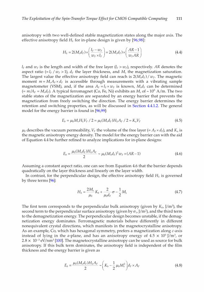
State-of-the-art MTJs are complex multilayer devices. Examples of MTJs include (from bottom to top): seed layer/PtMn/CoFeB/Ru/CoFeB/MgO/CoFeB/capping layer (an in-plane design with AFM and SAF) [109], Si wafer /Ta/Ru/Ta/CoFeB/MgO/CoFeB/Ta/Ru (an in-plane design without AFM or SAF) [44] and Ta/Ru/Ta/CoFeB/MgO/CoFeB/Ta/CoFeB/Ta/CoFeB/ MgO/Ta/Ru (interface perpendicular design, the MgO/CoFeB/Ta/CoFeB/ MgO cleverly doubles the energy barrier by doubling the interface anisotropy without increasing the switching current) [110]. The various designs are illustrated in Figure 4.11.
113The Exploitation of the Spin-Transfer Torque Effect for CMOS Compatible Computing
4.4.1.2 MTJ Properties
Memory devices are characterized by several key characteristics, such as endurance, reten-tion, power consumption, read/write time, and density.
4.4.1.2.1 Endurance
Assuming an access interval of 1 ns to 10 ns for a high performance memory, the memory will experience about 3 1016× operations for an expected operational lifetime of 10 years. Assuming further a 256 kiB memory density/64 B cache line (L2 cache [92]), an individ-ual memory cell is accessed about 1013 times. The number of times the memory is read is usually not a problem, but changing the state of a memory device can degrade the storage mechanism. As such, memories can wear out by repeated writing, and a cache memory should, therefore, withstand 1013 write operations. The endurance describes how many times a memory can be rewritten before the memory states become indis-tinguishable, which is a special reliability concern of memory devices. In a magnetic memory, the storage mechanism is the direction of magnetization in a ferromagnetic metal. There is no known degradation mechanism for the magnetization—the direction can be switched an in�nite number of times. Of more concern is the degradation of the tunneling barrier in MTJs, which can be degraded by current injection during writ-ing. However, for MRAM it has been demonstrated that it has “practically” unlimited endurance (>1012) [86,92,111].
FIGURE 4.11MTJ designs, where the reference layers are represented by big arrows and the free layers by small arrows. (a) An in-plane design, with the reference layer thicker than the free layer. (b) An interface perpendicular design, with the reference layer thinner than the free layer. (c) An in-plane design with a SAF. (d) An in-plane design with both a SAF and an AFM.
114 Energy Efficient Computing & Electronics
4.4.1.2.2 Retention, Volatility, and Thermal Stability
The distinction between a volatile and a nonvolatile memory is that the retention time, the time which the data is retained after power off, for nonvolatile memories is more than 10 years. MRAM belongs to the thermodynamically stable nonvolatile memory category, which means that the two possible states are approximately equally stable. Nevertheless, the memory is still susceptible to thermal �uctuations. The failure mecha-nism is modeled as [99]
1
=1
( / ).0τ τ
exp −E k Tb B (4.10)
τ is the mean time, τ0 the attempt period (approximately equal to the gyromagnetic resonance period [112], 10 10− −10 9− s), Eb the energy barrier (cf. Section 4.4.1.1), kB the Boltzmann constant, and T the absolute temperature. The ratio ∆H b BE k T= / is called the thermal stability factor and dimensionless. The thermally activated process is stochas-tic and the probability is modeled by the cumulative exponential distribution function:
p t t( ) = 1 ( / )− −exp τ (4.11)
Nonvolatile memories require less than one bit-�ip during 10 years (∼ 108 s), or p t Na( ) < 1/10 , where N is the number of bits in the memory. The required thermal stability factor can be estimated as
∆ =1
( /( 1)).10
0ln
lnt
N Na
τ×
−
(4.12)
For 64 MebiByte memory and an attempt period of 1 ns, the thermal stability factor must be larger than 60 to qualify as a nonvolatile memory. The thermal energy at room tempera-ture is approximately 26 meV; thus, the energy barrier must be larger than 1.56 eV. In prac-tice, the minimum energy barrier is taken at the maximum expected working temperature (∼80°C), in this case the energy barrier must be larger than 1.84 eV, or the thermal stability factor Δ > 71 at room temperature.
4.4.1.2.3 Writing and Critical Current
MRAM dissipates energy during writing in the form of Joule heating,
P RIJ = .2 (4.13)
PJ describes the dissipated power, R the resistance of the MTJ, and I the current. For STT-MTJs, the major dissipation occurs during writing, when the current is large. Thermal stability is modi�ed by the STT current [99,113,114]:
∆ ∆I Ic
I III
( ) = ( = 0) 1× −
(4.14)
Ic is the critical current density for switching. In microscopic models, it corresponds to the minimum spin torque required to reverse magnetization at absolute zero [113]. ∆ I is not necessarily identical with ∆H ; it has been shown experimentally that ∆ I is
115The Exploitation of the Spin-Transfer Torque Effect for CMOS Compatible Computing
smaller than ∆H [109]. If the temperature is nonzero, the MTJ can switch by thermal �uc-tuations, even if I Ic< . Obviously, also reducing the barrier leads to an increase in switch-ing probability. If one bit is written once every 100 ns for 10 years (3 1015× write operations), the probability of not switching must be below 3 10 16× − (= 1/3 1015× ). The necessary current as a function of pulse time can be estimated from
I t II
tp
p cI
p( ) = 11
( = 0)1
(1/ ).
0× − ×
∆
lnlnτ
(4.15)
Considering the assumptions from before, I Ic/ must be larger than 0.986 (∆ I = 71 ). The above formular is valid for thermally activated switching regimes (a few ns upwards). For shorter switching times, there is not suf�cient time for thermal excitations to aid the switching process and the switching changes towards the purely STT driven precessional switch-ing regime with a steeper current increase for shorter switching times [114]. Fast, reliable switching requires that the current is close to or larger than the critical current. The criti-cal current depends on the layer design, such as in-plane or perpendicular. For in-plane design, the critical current [21,96] is given by:
Iq
E M Vc b s Fin plane−
×
× +=
2(2 /2).0
2
αη
µ (4.16)
q describes the elementary charge, denotes the reduced Planck constant, α is the phenomenological Gilbert damping constant, and η the polarizing factor or spin-transfer ef�ciency. η depends on the spin polarization P and direction [115]:
η θθ
( , ) =2(1 ( ))2P
PP+ cos
(4.17)
θ = 0 describes the parallel and θ = π the anti-parallel state. η assumes its smallest value for the parallel state (large Ic). For the perpendicular design, the critical current is given by
Iq
Ec bperpendicular =2
2 .
×
×α
η (4.18)
Comparing the critical currents for in-plane and perpendicular designs shows that in-plane designs have an additional energy contribution that must be overcome. This term originates from the fact that the STT, which switches the in-plane magnetization, must move the magnetization out of the layer plane. The related energy barrier is µ0
2 /2M Vs F higher than the switching barrier Eb between the major and minor ellipses axis of the layer. Perpendicular designs do not need to overcome this extra energy barrier and, thus, exhibit lower critical currents.
Since both the retention time (Equation 4.10) and the critical current (Equations 4.16 and 4.18) depend on the energy barrier, there is a trade-off between high retention time and low critical current. A corresponding �gure of merit for an MTJ design is ∆H cI/ (the higher the better). The perpendicular design has a higher �gure of merit than the in-plane design, if all parameters are the same, since the perpendicular design, unlike the in-plane design, does not have to overcome the demagnetization �eld.
116 Energy Efficient Computing & Electronics
For a perpendicular layer CoFeB with a damping of 0.005 [93,96], an assumed spin polar-ization of 60% [104] in parallel state and an energy barrier of 1.8 eV, the critical current is 40 μA and its �gure of merit at room temperature (∆H cI/ ) is 1.7 μA−1. The resistance of an MTJ is on the order of 1–10 kΩ [93]; thus, the voltage and power dissipation when writ-ing is ∼100 mV and ∼1 μW, respectively. Given the switching time (∼10–100 ns), the energy consumed during writing is on the order of 10–100 fJ. Low energy operation (90 fJ write energy) has been experimentally demonstrated [93]. The most important material param-eters are damping and polarization.
4.4.1.2.4 Reading and TMR
Reading involves determining if the state is in a LRS or a HRS. The relevant metric is the TMR, given by Equation 4.3. The TMR is microscopically connected to the spin polarization P through Julliere’s model, which assumes that spin is conserved during tunneling [32].
∆GG
PPp
=2
1
2
2+ (4.19)
G is the conductance (= 1/R). Using Equation 4.3, Equation 4.19, and some algebra, the polarization can be estimated from the device TMR as
P TMR TMR= /( 2).+ (4.20)
An in�nitely high TMR corresponds to an ideal polarization of 1; thus, high polarization is important for material consideration. Polarization also improves the writability, as previ-ously discussed. The state is read by a sense current that develops a voltage drop across the MTJ. The magnitude of the voltage is used to determine the resistance state. Since a current passes through the MTJ during reading, power is dissipated and its magnetiza-tion is excited, which can lead to a read disturb error. A read disturb error is an accidental bit-�ip of a memory during the read operation. If one bit is read every 100 ns for 10 years (3 1015× read operations), the probability of switching must be below 3 10 16× − (= 1/3 1015× ). The read disturb error is a switching event due to thermal activation over the current reduced barrier. The maximum allowed sense current can be estimated from
I t II
tp
p cI
p( ) = 11
( = 0)1
(1/(1 )).
0× − ×
−
∆
lnlnτ
(4.21)
For a 10 ns read, I Ic/ must be smaller than 0.47, for a 1 ns read 0.5 ( )∆ I = 71 . Using the same values as for writing, the estimated sense voltage and dissipated power is on the order of 10–100 mV and 100 nW–1 μW. The time required to determine the state does not intrinsically depend on the MTJ but on the CMOS sense ampli�er. A large difference in resistance between HRS and LRS (corresponds to high TMR) allows trading-off sense ampli�er sensitivity to faster reading [96]. If the signal compared to noise is small, then the sense ampli�er must be more sensitive and will be comparatively slow [116]. It should be noted that for the most common memory architecture (1T-1R, see Section 4.4.3), the transistor is connected in series with the MTJ when reading. For instance, assuming a transistor impedance of 1 kΩ, an LRS of 1 kΩ and an HRS of 7 kΩ (TMR = 600%), the resistance ratio of the memory cell is 300%.
117The Exploitation of the Spin-Transfer Torque Effect for CMOS Compatible Computing
The reading operation is unipolar for all spintronic designs—only the magnitude of the voltage/current matters, not the sign.
4.4.1.2.5 Density and Scaling
Memory density is arguably the most important metric for commercial products. The den-sity is a measure of the number of bits per area, although it is often given by the number of bits per chip.
The density is not only determined by the size of the MTJ alone, but also by the size of the access device, typically a transistor (see Section 4.4.3). The size of the transistor is primarily determined by its drive current capability, which must be large enough to switch the MTJ (10–100 μA). The transistor width-normalized on-current for a low-power design transistor is about 600 μA/μm or A/m [116,117]. To provide 10–100 μA, the width has to be between 17 and 170 nm. For a hypothetical minimum sized memory cell (1T-1R) with a 20 nm memory half-pitch, the gate length would also be 20 nm (low-power logic transistor) [118]. The respective MTJ must be smaller than 20 nm and its switching current lower than 12 μA.
It is not trivial to take an MTJ design and scale it to smaller size. Looking at Equation 4.5 shows that decreasing the volume will cause a reduction in the energy barrier. To account for this decrease, the magnetic anisotropy strength has to be increased without degrading other parameters, for example like the damping by adding a second interface anisotropy [110]. The energy barrier and the switching current also depend on how the magnetiza-tion reversal takes place. Above a certain size (∼40–70 nm [21,96]), it is easiest to reverse the magnetization by �rst nucleating a new domain and then having it grow. However, for decreasing size the magnetization reversal becomes nucleation dominated and the ther-mal stability factor almost independent of size. The �gure of merit ∆H cI/ improves with decreasing size. Below ∼40–70 nm, the magnetic �lm prefers single-domain states and the entire domain switches instead of �rst growing a new domain. This is re�ected by a satu-ration in ∆H cI/ , as predicted by Equations 4.16 and 4.18 [96].
Most reports of MRAM circuits are on the order of Mib [94,95,109,119,120], and a few up to Gib [74,111].
4.4.1.2.6 Harsh Environment
There are applications where the electronics must be able to operate in harsh environments, such as military, vehicular, aerospace, space, and nuclear technology. The demands could be operation at low temperature (−40°C), high temperature (125°C), thermal cycling, and high radiation environment. Low temperature is not an issue for MTJ devices, as functional devices have been demonstrated to operate at liquid helium temperature (4 K). The spin-polarization through the tunneling layer is a function of temperature, and degrades with increasing temperature [121,122]. Nonvolatile operation at high temperature can be maintained as long as the thermal stability factor still exceeds about 60 at operation tem-perature. Or in other words the energy barrier must be about 30% larger as compared to room temperature (≈ 2eV or ∆H ≈ 78). MTJs are exceptionally radiation hard. Ionizing radiation cannot cause the magnetization to switch direction; thus, there are no single event upsets (SEU) [123] or loss of information. High enough radiation doses could cause displacement damage in the tunneling layer, which would degrade the overall mem-ory cell. Nevertheless, the real radiation vulnerability lies in the CMOS circuit. CMOS electronics would break at doses below the doses necessary to damage the MTJs [120]. But an SEU can cause transient currents in the CMOS periphery during reading the MTJ, which can lead to bit-�ip [124].
118 Energy Efficient Computing & Electronics
4.4.2 Magnetic Random Access Memory
This section covers different designs for spintronic memories. All of them share the same method of reading, the tunneling magnetoresistance effect. What distinguishes the designs is the way the memory state is switched. The designs covered here are thermally-assisted, STT, spin-Hall/spin-orbit, domain wall and �nally voltage controlled magnetic anisotropy (VCMA).
4.4.2.1 Thermally-Assisted MRAM
Thermally-assisted (TA) MRAM adds temperature as a controllable variable. The prin-ciple is quite simple—the thermal stability factor is smaller at a higher temperature and, therefore, it is easier to switch the state. This allows to design very stable devices at room temperature, without any penalty for writing, because the energy barrier for writing and the energy barrier responsible for the stability are decoupled by temperature.
Taken to the extreme, the device can undergo phase-changes during the writing pro-cedure. If the temperature is higher than the Curie temperature of the storage layer, it becomes paramagnetic. If the storage layer is cooled below the Curie temperature while biased into a state, it magnetizes easily into the biased state. Another design possibility is to couple the storage layer to an AFM. The storage layer can easily be switched, if the AFM is heated above its blocking temperature or Néel temperature (the AFM becomes paramagnetic), but is otherwise very dif�cult to switch [125]. Such devices are typically heated up to ∼200°C.
The devices proposed in [125] are for �eld-written MRAM, but TA-writing has also been demonstrated for STT-MTJs. The Joule dissipation is used to heat the storage layer (above 150°C). The perpendicular anisotropy of the storage layer is reduced, allowing the STT to bias the storage layer into a state. The anisotropy recovers as it cools down and the storage layer settles into the state it was biased into by the STT [126].
4.4.2.2 Spin-Transfer Torque MRAM
STT-based MRAM is the most mainstream design and was extensively covered in Section 4.4.1. A typical scaled memory device uses a perpendicular CoFeB/MgO/CoFeB stack, thanks to its low damping, high spin polarization, high TMR and low switching current. Gib-density has been demonstrated [74,111] and STT-MRAM is commercially available in density of 32Mib × 8 [95].
4.4.2.3 Spin-Hall/Spin-Orbit MRAM
The two-terminal MTJ suffers from its shared read- and write-path. A large write current can cause degradation in the tunneling layer, while reading can cause read disturb errors. The three-terminal Spin-Hall or Spin-Orbit MRAM offers a way to decouple the writing and reading path. The major bene�t is that the properties that determine reading and writing can be optimized independently of each other. The reading is still carried out by the TMR-effect, but the writing is performed by spin injection from a heavy-metal �lm by utilizing the SHE. The reference layer has one terminal, and the heavy-metal �lm has two terminals.
The SHE details have been explained in Section 4.2.3. Metals generating a spin-current are Ta [127,128], W [129], Ir-doped Cu [130], and several others [131]. There are differences
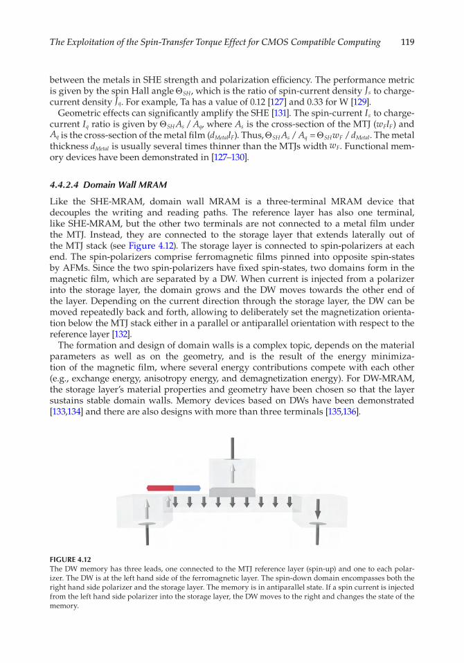
119The Exploitation of the Spin-Transfer Torque Effect for CMOS Compatible Computing
between the metals in SHE strength and polarization ef�ciency. The performance metric is given by the spin Hall angle ΘSH, which is the ratio of spin-current density Js to charge-current density Jq. For example, Ta has a value of 0.12 [127] and 0.33 for W [129].
Geometric effects can signi�cantly amplify the SHE [131]. The spin-current Is to charge-current Iq ratio is given by ΘSH s qA A/ , where As is the cross-section of the MTJ (w lF F) and Aq is the cross-section of the metal �lm (d lMetal F). Thus, Θ ΘSH s q SH F MetalA A w d/ = / . The metal thickness dMetal is usually several times thinner than the MTJs width wF. Functional mem-ory devices have been demonstrated in [127–130].
4.4.2.4 Domain Wall MRAM
Like the SHE-MRAM, domain wall MRAM is a three-terminal MRAM device that decouples the writing and reading paths. The reference layer has also one terminal, like SHE-MRAM, but the other two terminals are not connected to a metal �lm under the MTJ. Instead, they are connected to the storage layer that extends laterally out of the MTJ stack (see Figure 4.12). The storage layer is connected to spin-polarizers at each end. The spin-polarizers comprise ferromagnetic �lms pinned into opposite spin-states by AFMs. Since the two spin-polarizers have �xed spin-states, two domains form in the magnetic �lm, which are separated by a DW. When current is injected from a polarizer into the storage layer, the domain grows and the DW moves towards the other end of the layer. Depending on the current direction through the storage layer, the DW can be moved repeatedly back and forth, allowing to deliberately set the magnetization orienta-tion below the MTJ stack either in a parallel or antiparallel orientation with respect to the reference layer [132].
The formation and design of domain walls is a complex topic, depends on the material parameters as well as on the geometry, and is the result of the energy minimiza-tion of the magnetic �lm, where several energy contributions compete with each other (e.g., exchange energy, anisotropy energy, and demagnetization energy). For DW-MRAM, the storage layer’s material properties and geometry have been chosen so that the layer sustains stable domain walls. Memory devices based on DWs have been demonstrated [133,134] and there are also designs with more than three terminals [135,136].
FIGURE 4.12The DW memory has three leads, one connected to the MTJ reference layer (spin-up) and one to each polar-izer. The DW is at the left hand side of the ferromagnetic layer. The spin-down domain encompasses both the right hand side polarizer and the storage layer. The memory is in antiparallel state. If a spin current is injected from the left hand side polarizer into the storage layer, the DW moves to the right and changes the state of the memory.
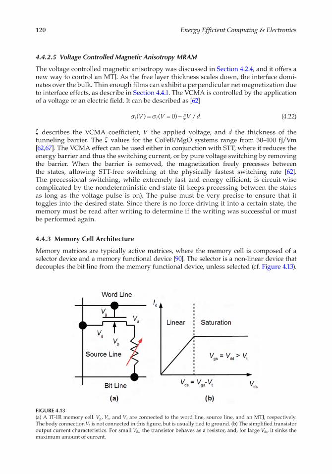
120 Energy Efficient Computing & Electronics
4.4.2.5 Voltage Controlled Magnetic Anisotropy MRAM
The voltage controlled magnetic anisotropy was discussed in Section 4.2.4, and it offers a new way to control an MTJ. As the free layer thickness scales down, the interface domi-nates over the bulk. Thin enough �lms can exhibit a perpendicular net magnetization due to interface effects, as describe in Section 4.4.1. The VCMA is controlled by the application of a voltage or an electric �eld. It can be described as [62]
σ σ ξi iV V V d( ) = ( = 0) / .− (4.22)
ξ describes the VCMA coef�cient, V the applied voltage, and d the thickness of the tunneling barrier. The ξ values for the CoFeB/MgO systems range from 30–100 fJ/Vm [62,67]. The VCMA effect can be used either in conjunction with STT, where it reduces the energy barrier and thus the switching current, or by pure voltage switching by removing the barrier. When the barrier is removed, the magnetization freely precesses between the states, allowing STT-free switching at the physically fastest switching rate [62]. The precessional switching, while extremely fast and energy ef�cient, is circuit-wise complicated by the nondeterministic end-state (it keeps precessing between the states as long as the voltage pulse is on). The pulse must be very precise to ensure that it toggles into the desired state. Since there is no force driving it into a certain state, the memory must be read after writing to determine if the writing was successful or must be performed again.
4.4.3 Memory Cell Architecture
Memory matrices are typically active matrices, where the memory cell is composed of a selector device and a memory functional device [90]. The selector is a non-linear device that decouples the bit line from the memory functional device, unless selected (cf. Figure 4.13).
FIGURE 4.13(a) A 1T-1R memory cell. Vg , Vs, and Vd are connected to the word line, source line, and an MTJ, respectively. The body connection Vb is not connected in this �gure, but is usually tied to ground. (b) The simpli�ed transistor output current characteristics. For small Vds, the transistor behaves as a resistor, and, for large Vds, it sinks the maximum amount of current.
121The Exploitation of the Spin-Transfer Torque Effect for CMOS Compatible Computing
Examples of selector devices are diodes (PN, Schottky) and transistors (NPN, NMOS, and PMOS). Diodes are preferred for their smaller size over transistors, but their rectifying property limits the memory functional device to the unipolar class. NMOS and PMOS transistors are used for bipolar class memories. NMOS transistors are preferred over PMOS transistors because they deliver larger currents for a given size due to their higher charge carrier mobility.
The access transistor is a four terminal (gate, source, drain, and body) device for a bulk CMOS process and a three terminal device for a silicon on insulator (SOI) process (gate, source, and drain). The body of the bulk transistor is connected to the lowest potential for an NMOS device (typically ground) and the highest potential for a PMOS device (typically Vdd). The transistor is characterized by its threshold voltage Vt. The NMOS transistor is on, when the source-gate voltage V V Vgs g s= − is larger than Vt and off if smaller than Vt (for the PMOS it is the opposite, and Vt is negative). The maxi-mum current through a long-channel transistor occurs, when the transistor is on (V V Vgs t ov− = > 0) and the source-drain voltage V V Vds d s= − is larger than the overdrive voltage Vov. The transistor operates in saturation and is approximately independent of Vds as long as the saturation condition is met. Since STT-switched MTJs require large currents, the transistor may operate in saturation during programming. For small Vds, the transistor operates in the linear region and behaves as a resistor with an impedance on the order 100 Ω–1 kΩ. The transistor is operated in the linear region during reading. Figure 4.13 shows the transistor connected to an MTJ and the transistor output current characteristics.
The most basic CMOS circuit has only two potentials, ground and Vdd. The power sup-ply depends on the CMOS technology and its intended application, but is in the range of 1.2–3.3 V for submicron transistors. A necessary but not suf�cient condition for turning the NMOS transistor on is that the gate potential is Vdd. The NMOS transistor can still be off, if the source potential is larger than V Vdd t− , since V V V V V V Vgs g s dd dd t t= < ( ) =− − − . This condition can occur for the access NMOS transistor, if it tries to source a large cur-rent to a large resistor, such as in the case of programming an MTJ with high resistance. The equivalent case for a PMOS transistor solution is when it tries to sink a current. This condition is known as source degeneration. There are several ways to avoid this. A charge pump can boost the gate voltage to V Vdd t+ , in such case, a full Vdd voltage-drop can be applied to the MTJ. But the charge pump solution is less preferably, as it consumes extra overhead area, power, and adds circuit complexity [99]. The largest current occurs during writing P→AP, when the current is sourced through the reference layer. For this case, it is best to connect the highest potential to the reference layer, or in other words, to connect the reference layer to the bit line. Consequently, the free layer is then connected to the drain of the NMOS transistor, which sinks current to the source line during the P→AP transition. Another solution is to use a PMOS transistor [91], where the drain is connected to the reference layer. The PMOS transistor will not have any source degeneration, when it sources the current during the P→AP transition, since the source is connected to the highest potential.
MRAM devices can be separated into devices with unipolar and bipolar switching. Most, but not all, MRAM devices are two-terminal devices. If there are multiple terminals, they are typically connected to different transistors. As such, MRAM can be realized by several memory cell architectures, such as 1D-1R, 1T-1R, 2T-1R, or 2T-2R (D = Diode, T = Transistor, R = Resistor, sometimes referred to as MTJ in literature). There are even more memory cell architectures, like 6T-2R, which will be brie�y covered in Section 4.7.
122 Energy Efficient Computing & Electronics
1D-1R: This is the smallest memory cell for spin-based memories, with a minimum cell size of 4F2. F refers to the half-pitch in DRAM memory (2F = width + spacing = pitch), and is connected to the minimum lithographic feature size. It requires that the MTJ itself is not larger than 4F2 and can be placed on-top of the diode. A requirement of this memory cell is that the MTJ allows unipolar switching, which is possible for the orthogonal MTJ design (cf. [137,138]) and devices using VCMA [62]. The cell is selected (selector in low-impedance state), when there is a voltage drop across the diode (about 0.2 V for a Schottky and 0.7 V for a PN).
1T-1R: This is the standard memory cell for spin-based memories, shown in Figure 4.13. The 1T-1R is super�cially similar to the 1T-1C of the DRAM. The densest DRAM cell uses an open architecture with a transistor size of 6F2. The size is minimized by having one contact shared between two transistors. It has been argued that the 1T-1R cell can be as small as 6F2 at the 90 nm node by [99], 9F2 at 45 nm feature size [74], and 22F2 was demonstrated at 28 nm feature size [111].
2T-1R: This cell design is used for three-terminal spintronic devices, like SHE-MRAM (Section 4.4.2.3) and DW-MRAM (Section 4.4.2.4). The size is larger or equal to 12F2, as transistors cannot share their contacts [134]. These devices target SRAM replacement instead of DRAM replacement [135].
2T-2R: This cell should be interpreted as 2×1T-1R. It dedicates “two” 1T-1R cells to store the data and their complement. The minimum size is larger or equal to 12F2. The memory density is about half of designs with1T-1R cells. This is a major dis-advantage, but the design offers some performance advantages. The storing of both the data and its complement effectively doubles the read signal and allows to trade sensitivity for fast differential reading (see Section 4.4.1.2). It is also very robust to process variations. The performance of individual MTJs is strongly cor-related to their locality, because MTJs near each other are more likely to show the same performance compared to MTJs further apart. As such, the RP and RAP of the two MTJs are very likely a close match, which almost guarantees correct reading. For example, it is highly unlikely that the RP of one MTJ is as high as the RAP of the adjacent MTJ, or conversely that the RAP is as low as the RP of the adjacent MTJ. For large arrays, the spread of values of RP and RAP in 1T-1R designs must be very small (i.e., 20 <σ R RAP P− [96,99]) to ensure that min( )RAP of the array can never be mis-interpreted as parallel state, and that max( )RP of the array is not misinterpreted as antiparallel state. An example of a 2T-2R design can be found in [94], using a 90 nm CMOS process.
4.5 Spintronic Logic
As explained in the previous sections spintronic devices, in particular MTJs, are very promising for memory applications due to their nonvolatility, CMOS-compatibility, fast operation, and (nearly) unlimited endurance. But they are by no means limited to pure memory applications, which is re�ected in the ITRS [118], where it is suggested to exploit nonvolatile devices to circumvent current limits of state-of-the-art logic circuits. Among
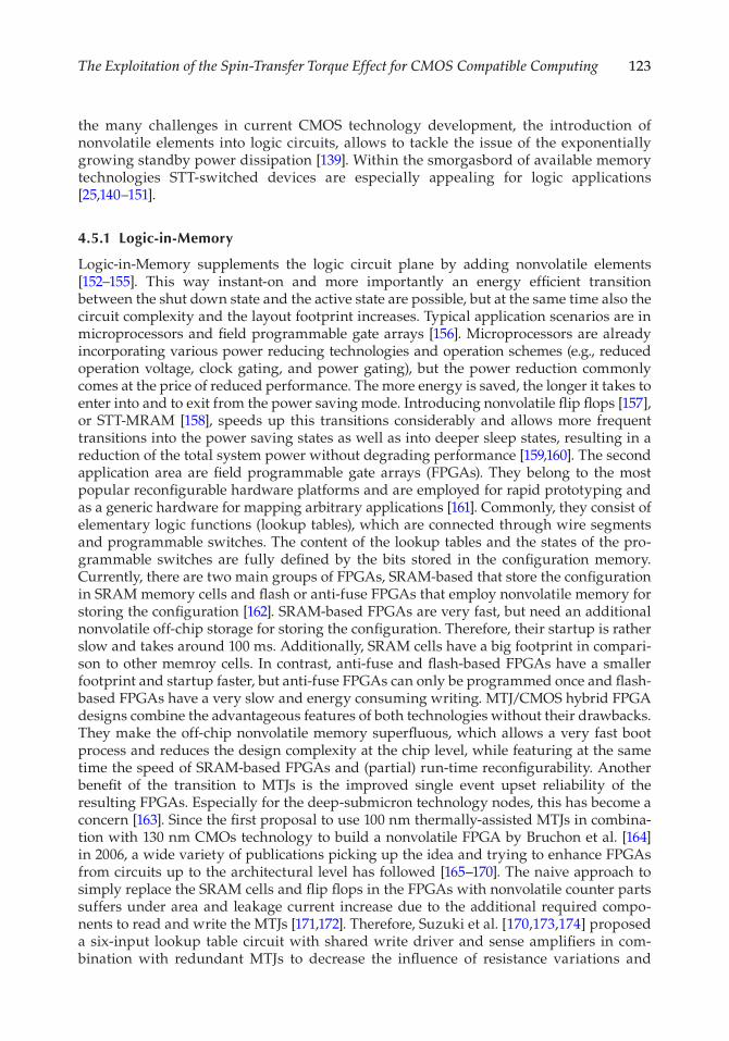
123The Exploitation of the Spin-Transfer Torque Effect for CMOS Compatible Computing
the many challenges in current CMOS technology development, the introduction of nonvolatile elements into logic circuits, allows to tackle the issue of the exponentially growing standby power dissipation [139]. Within the smorgasbord of available memory technologies STT-switched devices are especially appealing for logic applications [25,140–151].
4.5.1 Logic-in-Memory
Logic-in-Memory supplements the logic circuit plane by adding nonvolatile elements [152–155]. This way instant-on and more importantly an energy ef�cient transition between the shut down state and the active state are possible, but at the same time also the circuit complexity and the layout footprint increases. Typical application scenarios are in microprocessors and �eld programmable gate arrays [156]. Microprocessors are already incorporating various power reducing technologies and operation schemes (e.g., reduced operation voltage, clock gating, and power gating), but the power reduction commonly comes at the price of reduced performance. The more energy is saved, the longer it takes to enter into and to exit from the power saving mode. Introducing nonvolatile �ip �ops [157], or STT-MRAM [158], speeds up this transitions considerably and allows more frequent transitions into the power saving states as well as into deeper sleep states, resulting in a reduction of the total system power without degrading performance [159,160]. The second application area are �eld programmable gate arrays (FPGAs). They belong to the most popular recon�gurable hardware platforms and are employed for rapid prototyping and as a generic hardware for mapping arbitrary applications [161]. Commonly, they consist of elementary logic functions (lookup tables), which are connected through wire segments and programmable switches. The content of the lookup tables and the states of the pro-grammable switches are fully de�ned by the bits stored in the con�guration memory. Currently, there are two main groups of FPGAs, SRAM-based that store the con�guration in SRAM memory cells and �ash or anti-fuse FPGAs that employ nonvolatile memory for storing the con�guration [162]. SRAM-based FPGAs are very fast, but need an additional nonvolatile off-chip storage for storing the con�guration. Therefore, their startup is rather slow and takes around 100 ms. Additionally, SRAM cells have a big footprint in compari-son to other memroy cells. In contrast, anti-fuse and �ash-based FPGAs have a smaller footprint and startup faster, but anti-fuse FPGAs can only be programmed once and �ash-based FPGAs have a very slow and energy consuming writing. MTJ/CMOS hybrid FPGA designs combine the advantageous features of both technologies without their drawbacks. They make the off-chip nonvolatile memory super�uous, which allows a very fast boot process and reduces the design complexity at the chip level, while featuring at the same time the speed of SRAM-based FPGAs and (partial) run-time recon�gurability. Another bene�t of the transition to MTJs is the improved single event upset reliability of the resulting FPGAs. Especially for the deep-submicron technology nodes, this has become a concern [163]. Since the �rst proposal to use 100 nm thermally-assisted MTJs in combina-tion with 130 nm CMOs technology to build a nonvolatile FPGA by Bruchon et al. [164] in 2006, a wide variety of publications picking up the idea and trying to enhance FPGAs from circuits up to the architectural level has followed [165–170]. The naive approach to simply replace the SRAM cells and �ip �ops in the FPGAs with nonvolatile counter parts suffers under area and leakage current increase due to the additional required compo-nents to read and write the MTJs [171,172]. Therefore, Suzuki et al. [170,173,174] proposed a six-input lookup table circuit with shared write driver and sense ampli�ers in com-bination with redundant MTJs to decrease the in�uence of resistance variations and
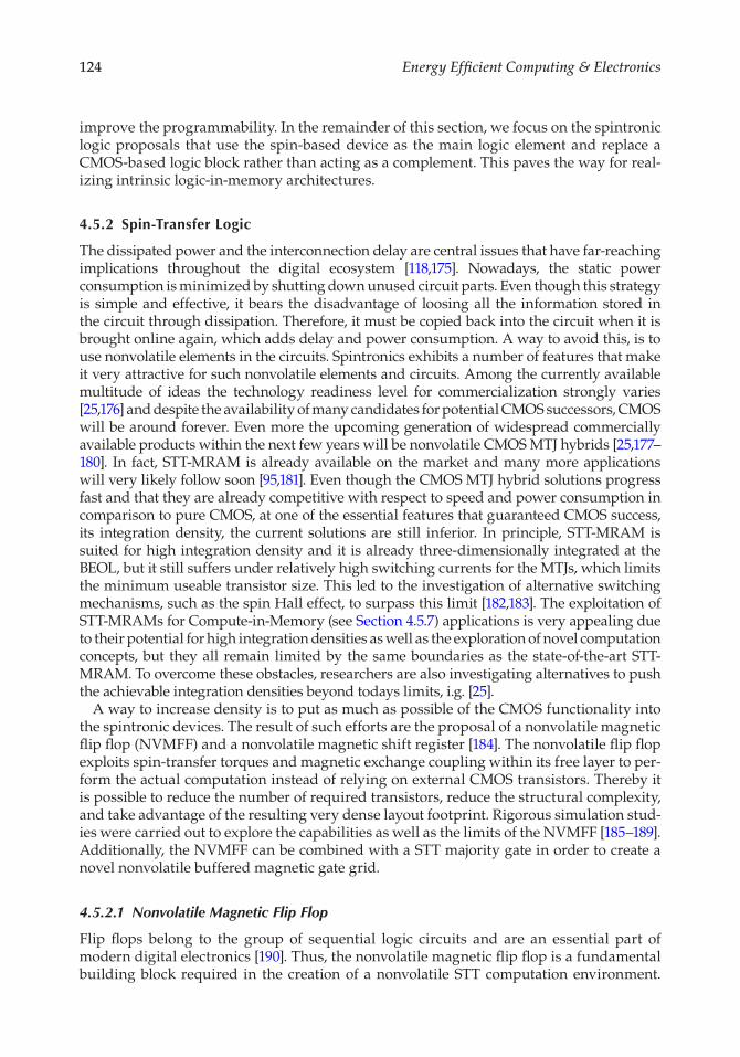
124 Energy Efficient Computing & Electronics
improve the programmability. In the remainder of this section, we focus on the spintronic logic proposals that use the spin-based device as the main logic element and replace a CMOS-based logic block rather than acting as a complement. This paves the way for real-izing intrinsic logic-in-memory architectures.
4.5.2 Spin-Transfer Logic
The dissipated power and the interconnection delay are central issues that have far-reaching implications throughout the digital ecosystem [118,175]. Nowadays, the static power consumption is minimized by shutting down unused circuit parts. Even though this strategy is simple and effective, it bears the disadvantage of loosing all the information stored in the circuit through dissipation. Therefore, it must be copied back into the circuit when it is brought online again, which adds delay and power consumption. A way to avoid this, is to use nonvolatile elements in the circuits. Spintronics exhibits a number of features that make it very attractive for such nonvolatile elements and circuits. Among the currently available multitude of ideas the technology readiness level for commercialization strongly varies [25,176] and despite the availability of many candidates for potential CMOS successors, CMOS will be around forever. Even more the upcoming generation of widespread commercially available products within the next few years will be nonvolatile CMOS MTJ hybrids [25,177–180]. In fact, STT-MRAM is already available on the market and many more applications will very likely follow soon [95,181]. Even though the CMOS MTJ hybrid solutions progress fast and that they are already competitive with respect to speed and power consumption in comparison to pure CMOS, at one of the essential features that guaranteed CMOS success, its integration density, the current solutions are still inferior. In principle, STT-MRAM is suited for high integration density and it is already three-dimensionally integrated at the BEOL, but it still suffers under relatively high switching currents for the MTJs, which limits the minimum useable transistor size. This led to the investigation of alternative switching mechanisms, such as the spin Hall effect, to surpass this limit [182,183]. The exploitation of STT-MRAMs for Compute-in-Memory (see Section 4.5.7) applications is very appealing due to their potential for high integration densities as well as the exploration of novel computation concepts, but they all remain limited by the same boundaries as the state-of-the-art STT-MRAM. To overcome these obstacles, researchers are also investigating alternatives to push the achievable integration densities beyond todays limits, i.g. [25].
A way to increase density is to put as much as possible of the CMOS functionality into the spintronic devices. The result of such efforts are the proposal of a nonvolatile magnetic �ip �op (NVMFF) and a nonvolatile magnetic shift register [184]. The nonvolatile �ip �op exploits spin-transfer torques and magnetic exchange coupling within its free layer to per-form the actual computation instead of relying on external CMOS transistors. Thereby it is possible to reduce the number of required transistors, reduce the structural complexity, and take advantage of the resulting very dense layout footprint. Rigorous simulation stud-ies were carried out to explore the capabilities as well as the limits of the NVMFF [185–189]. Additionally, the NVMFF can be combined with a STT majority gate in order to create a novel nonvolatile buffered magnetic gate grid.
4.5.2.1 Nonvolatile Magnetic Flip Flop
Flip �ops belong to the group of sequential logic circuits and are an essential part of modern digital electronics [190]. Thus, the nonvolatile magnetic �ip �op is a fundamental building block required in the creation of a nonvolatile STT computation environment.
125The Exploitation of the Spin-Transfer Torque Effect for CMOS Compatible Computing
Therefore, we will �rst explain how a single NVMFF works and use this knowledge later as basis for more complex applications, such as a nonvolatile shift register or a nonvola-tile buffered gate grid. The NVMFF comprises three antiferromagnetically coupled polar-izer stacks with perpendicular magnetization orientation (see Figure 4.14). The polarizer stacks are connected with each other through nonmagnetic interconnection layers (e.g., MgO, Al2O3 or Cu) and a common free layer with perpendicular magnetization orien-tation. One of the stacks is used for readout Q and the remaining two are dedicated to input A and B. Due to the anti-ferromagnetic nature of the polarizer stacks it is assumed that their stray �eld is negligible. The information is stored as magnetization orientation of the shared free layer and accessible via GMR or TMR effect. Depending on the rela-tive orientation between the magnetization orientation of the shared free layer and the readout stack Q a high resistance state HRS (antiparallel) or a low resistance state LRS (parallel) is measured. The respective HRS and LRS are assigned to logic “0” and logic “1,” respectively. For the operation of a single NVMFF, the polarity of the input pulses is mapped to logic “0” and “1.” If now, a negative voltage is applied to one of the inputs (i.e., A), then electrons will �ow from the leads through the polarizer stack, where they align with the local magnetization orientation, and eventually enter the common free layer before they get absorbed by the grounded bottom contact. During their time in the com-mon free layer, the electrons relax to the free layers magnetization orientation. This cre-ates a localized torque in the region where the electrons traverse, which depends on the pulse polarity and the relative orientation between the layers. Depending on the electrons polarization orientation the exerted torque either tries to push the magnetization into its other stable position or damps the magnetization precessions and stabilizes its current orientation. For the operation of the �ip �op, two synchronous input pulses are applied to the two inputs A and B. Both pulses exert an STT on the common free layer. For �xed parallel magnetization orientations of the two input stacks and two input pulse polarities, four input combinations are feasible. Depending on the input pulse polarities the two cre-ated STTs either add up and accelerate the switching (same polarity) or counter act each other and damp the switching ( opposing polarities). Translating this behavior to a logic table shows that the device can be SET/RESET (same polarity) as well as HOLD its current
FIGURE 4.14The nonvolatile magnetic �ip �op comprises three MTJ or spin valve stacks that share a common magnetic free layer. It is operated by two simultaneously applied current pulses at its inputs A and B. Logic “0” and “1” are encoded via the pulse polarity and the result of each operation is stored in the common free layer as the layer’s magnetization orientation. The information stored in the �ip �op is accessible through its output Q as a high or low resistance state by exploiting either the GMR or the TMR effect.
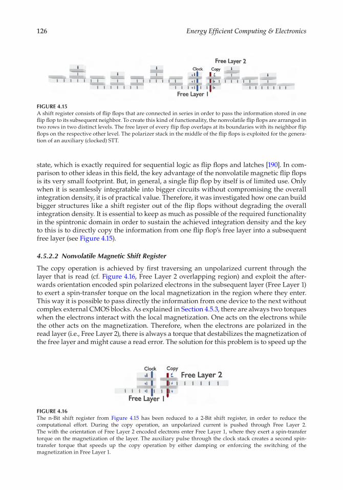
126 Energy Efficient Computing & Electronics
state, which is exactly required for sequential logic as �ip �ops and latches [190]. In com-parison to other ideas in this �eld, the key advantage of the nonvolatile magnetic �ip �ops is its very small footprint. But, in general, a single �ip �op by itself is of limited use. Only when it is seamlessly integratable into bigger circuits without compromising the overall integration density, it is of practical value. Therefore, it was investigated how one can build bigger structures like a shift register out of the �ip �ops without degrading the overall integration density. It is essential to keep as much as possible of the required functionality in the spintronic domain in order to sustain the achieved integration density and the key to this is to directly copy the information from one �ip �op’s free layer into a subsequent free layer (see Figure 4.15).
4.5.2.2 Nonvolatile Magnetic Shift Register
The copy operation is achieved by �rst traversing an unpolarized current through the layer that is read (cf. Figure 4.16, Free Layer 2 overlapping region) and exploit the after-wards orientation encoded spin polarized electrons in the subsequent layer (Free Layer 1) to exert a spin-transfer torque on the local magnetization in the region where they enter. This way it is possible to pass directly the information from one device to the next without complex external CMOS blocks. As explained in Section 4.5.3, there are always two torques when the electrons interact with the local magnetization. One acts on the electrons while the other acts on the magnetization. Therefore, when the electrons are polarized in the read layer (i.e., Free Layer 2), there is always a torque that destabilizes the magnetization of the free layer and might cause a read error. The solution for this problem is to speed up the
FIGURE 4.16The n-Bit shift register from Figure 4.15 has been reduced to a 2-Bit shift register, in order to reduce the computational effort. During the copy operation, an unpolarized current is pushed through Free Layer 2. The with the orientation of Free Layer 2 encoded electrons enter Free Layer 1, where they exert a spin- transfer torque on the magnetization of the layer. The auxiliary pulse through the clock stack creates a second spin- transfer torque that speeds up the copy operation by either damping or enforcing the switching of the magnetization in Free Layer 1.
FIGURE 4.15A shift register consists of �ip �ops that are connected in series in order to pass the information stored in one �ip �op to its subsequent neighbor. To create this kind of functionality, the nonvolatile �ip �ops are arranged in two rows in two distinct levels. The free layer of every �ip �op overlaps at its boundaries with its neighbor �ip �ops on the respective other level. The polarizer stack in the middle of the �ip �ops is exploited for the genera-tion of an auxiliary (clocked) STT.
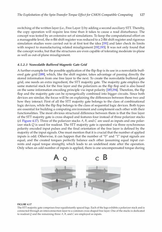
127The Exploitation of the Spin-Transfer Torque Effect for CMOS Compatible Computing
switching of the written layer (i.e., Free Layer 1) by adding a second auxiliary STT. Thereby, the copy operation will require less time than it takes to cause a read disturbance. The concept was tested by an extensive set of simulations. To keep the computational effort on a manageable level, the n-Bit shift register was reduced to a 2-Bit shift register and rigorous simulation studies were carried out to at �rst test the idea [191] and later check its limits with respect to manufacturing related misalignment [192,193]. It was not only found that the concept works, but that the structures are even capable of tolerating moderate in-plane as well as out-of-plane misalignment.
4.5.2.3 Nonvolatile Buffered Magnetic Gate Grid
A further example for the possible application of the �ip �op is its use in a nonvolatile buff-ered gate grid [189], which, like the shift register, takes advantage of passing directly the stored information from one free layer to the next. To create the nonvolatile buffered gate grid, one needs an extra ingredient, the STT majority gate. The majority gate employs the same material stack for the free layer and the polarizers as the �ip �op and is also based on the same information encoding principle via input polarity [185,194]. Therefore, the �ip �op and the majority gate can be synergetically combined into bigger circuits. Since both devices are similar, the focus will be on explaining the differences between these two and how they interact. First of all the STT majority gate belongs to the class of combinational logic devices, while the �ip �op belongs to the class of sequential logic devices. Both types are essential for building a computing environment and complement each other with their functionalities. The most obvious structural difference between them is that the free layer of the STT majority gate is cross shaped and features four instead of three polarizer stacks (cf. Figure 4.17). Three of the polarizer stacks A, B, and C are used as inputs and one polar-izer stack Q is used for readout. The STT majority gate is operated via three synchronous polarity encoded input pulses and the �nal orientation of the free layer is de�ned by the majority of the input signals. One must mention that it is crucial that the number of applied inputs is odd. Otherwise, it can happen that the number of “0” and “1” input signals are equal, and the created torques perfectly balance each other (assuming equal input cur-rents and equal torque strength), which leads to an unde�ned state after the operation. Only when an odd number of inputs is applied, there is one uncompensated torque during
FIGURE 4.17The STT majority gate comprises four equidistantly spaced legs. Each of the legs exhibits a polarizer stack and is connected through an interconnection layer to a common cross shaped free layer. One of the stacks is dedicated to readout Q and the remaining three A, B, and C are employed as inputs.
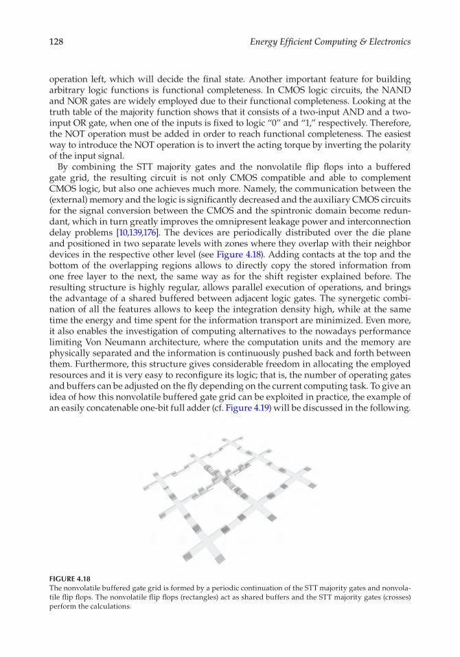
128 Energy Efficient Computing & Electronics
operation left, which will decide the �nal state. Another important feature for building arbitrary logic functions is functional completeness. In CMOS logic circuits, the NAND and NOR gates are widely employed due to their functional completeness. Looking at the truth table of the majority function shows that it consists of a two-input AND and a two-input OR gate, when one of the inputs is �xed to logic “0” and “1,” respectively. Therefore, the NOT operation must be added in order to reach functional completeness. The easiest way to introduce the NOT operation is to invert the acting torque by inverting the polarity of the input signal.
By combining the STT majority gates and the nonvolatile �ip �ops into a buffered gate grid, the resulting circuit is not only CMOS compatible and able to complement CMOS logic, but also one achieves much more. Namely, the communication between the (external) memory and the logic is signi�cantly decreased and the auxiliary CMOS circuits for the signal conversion between the CMOS and the spintronic domain become redun-dant, which in turn greatly improves the omnipresent leakage power and interconnection delay problems [10,139,176]. The devices are periodically distributed over the die plane and positioned in two separate levels with zones where they overlap with their neighbor devices in the respective other level (see Figure 4.18). Adding contacts at the top and the bottom of the overlapping regions allows to directly copy the stored information from one free layer to the next, the same way as for the shift register explained before. The resulting structure is highly regular, allows parallel execution of operations, and brings the advantage of a shared buffered between adjacent logic gates. The synergetic combi-nation of all the features allows to keep the integration density high, while at the same time the energy and time spent for the information transport are minimized. Even more, it also enables the investigation of computing alternatives to the nowadays performance limiting Von Neumann architecture, where the computation units and the memory are physically separated and the information is continuously pushed back and forth between them. Furthermore, this structure gives considerable freedom in allocating the employed resources and it is very easy to recon�gure its logic; that is, the number of operating gates and buffers can be adjusted on the �y depending on the current computing task. To give an idea of how this nonvolatile buffered gate grid can be exploited in practice, the example of an easily concatenable one-bit full adder (cf. Figure 4.19) will be discussed in the following.
FIGURE 4.18The nonvolatile buffered gate grid is formed by a periodic continuation of the STT majority gates and nonvola-tile �ip �ops. The nonvolatile �ip �ops (rectangles) act as shared buffers and the STT majority gates (crosses) perform the calculations.
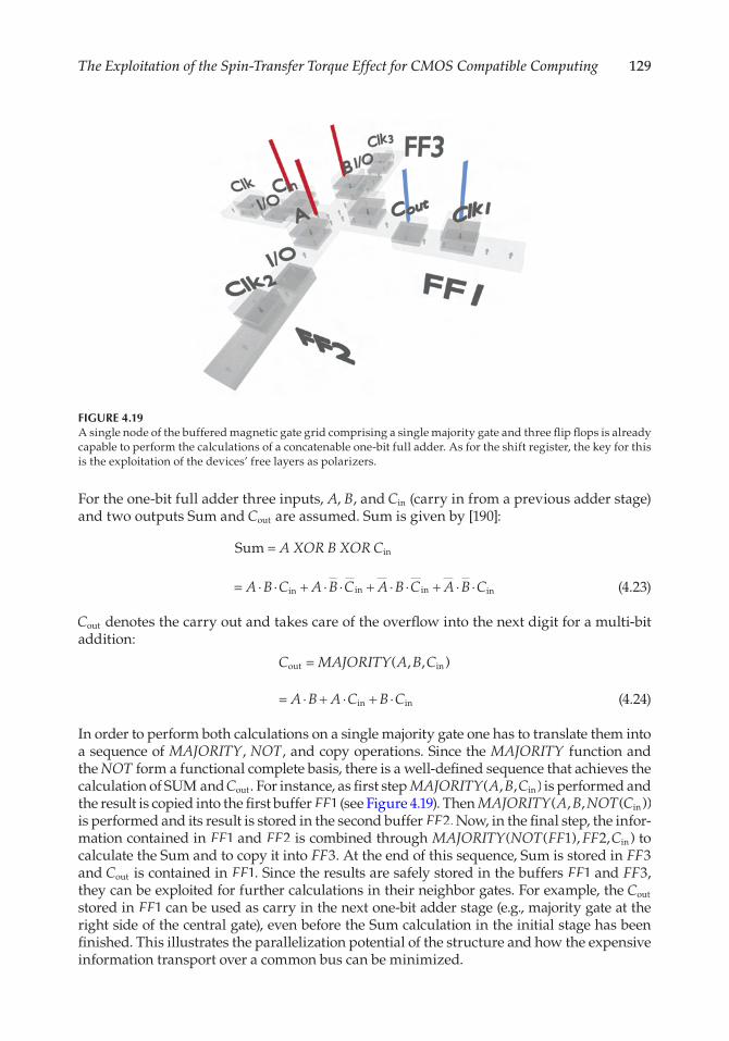
129The Exploitation of the Spin-Transfer Torque Effect for CMOS Compatible Computing
For the one-bit full adder three inputs, A, B, and Cin (carry in from a previous adder stage) and two outputs Sum and Cout are assumed. Sum is given by [190]:
Sum in= A XOR B XOR C
= A B C A B C A B C A B C⋅ ⋅ + ⋅ ⋅ + ⋅ ⋅ + ⋅ ⋅in in in in (4.23)
Cout denotes the carry out and takes care of the over�ow into the next digit for a multi-bit addition:
C MAJORITY A B Cout in= ( , , )
= A B A C B C⋅ + ⋅ + ⋅in in (4.24)
In order to perform both calculations on a single majority gate one has to translate them into a sequence of MAJORITY, NOT, and copy operations. Since the MAJORITY function and the NOT form a functional complete basis, there is a well-de�ned sequence that achieves the calculation of SUM and Cout. For instance, as �rst step MAJORITY A B C( , , )in is performed and the result is copied into the �rst buffer FF1 (see Figure 4.19). Then MAJORITY A B NOT C( , , ( ))in is performed and its result is stored in the second buffer FF2. Now, in the �nal step, the infor-mation contained in FF1 and FF2 is combined through MAJORITY NOT FF FF C( ( 1), 2, )in to calculate the Sum and to copy it into FF3. At the end of this sequence, Sum is stored in FF3 and Cout is contained in FF1. Since the results are safely stored in the buffers FF1 and FF3, they can be exploited for further calculations in their neighbor gates. For example, the Cout stored in FF1 can be used as carry in the next one-bit adder stage (e.g., majority gate at the right side of the central gate), even before the Sum calculation in the initial stage has been �nished. This illustrates the parallelization potential of the structure and how the expensive information transport over a common bus can be minimized.
FIGURE 4.19A single node of the buffered magnetic gate grid comprising a single majority gate and three �ip �ops is already capable to perform the calculations of a concatenable one-bit full adder. As for the shift register, the key for this is the exploitation of the devices’ free layers as polarizers.
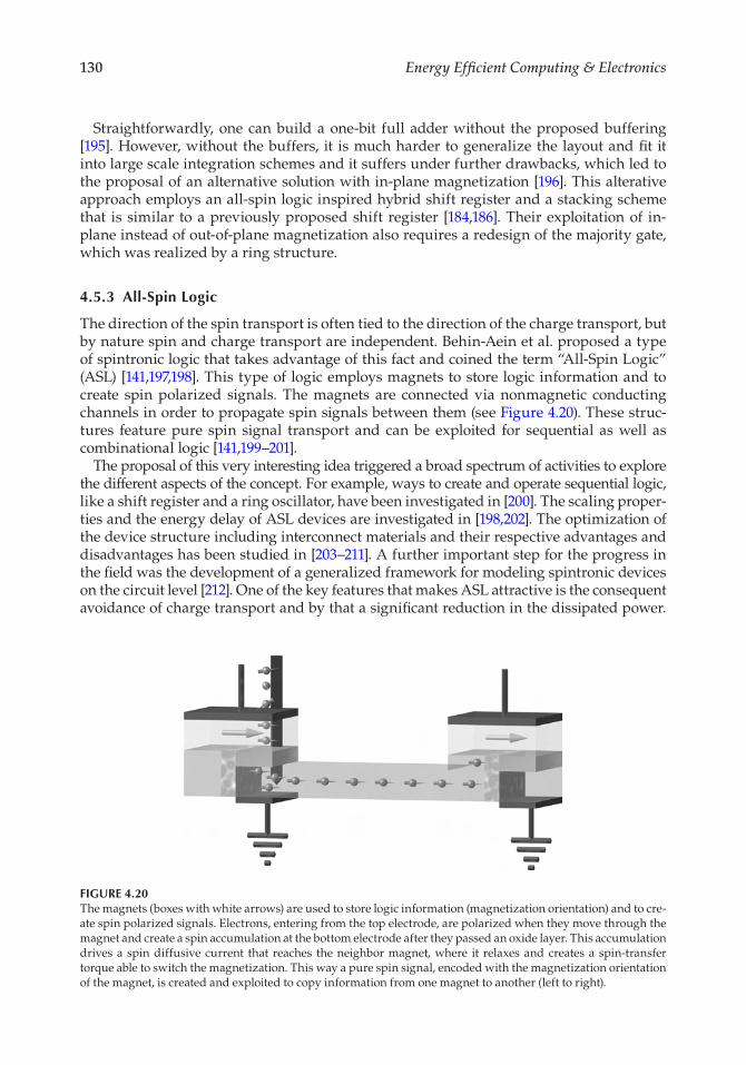
130 Energy Efficient Computing & Electronics
Straightforwardly, one can build a one-bit full adder without the proposed buffering [195]. However, without the buffers, it is much harder to generalize the layout and �t it into large scale integration schemes and it suffers under further drawbacks, which led to the proposal of an alternative solution with in-plane magnetization [196]. This alterative approach employs an all-spin logic inspired hybrid shift register and a stacking scheme that is similar to a previously proposed shift register [184,186]. Their exploitation of in-plane instead of out-of-plane magnetization also requires a redesign of the majority gate, which was realized by a ring structure.
4.5.3 All-Spin Logic
The direction of the spin transport is often tied to the direction of the charge transport, but by nature spin and charge transport are independent. Behin-Aein et al. proposed a type of spintronic logic that takes advantage of this fact and coined the term “All-Spin Logic” (ASL) [141,197,198]. This type of logic employs magnets to store logic information and to create spin polarized signals. The magnets are connected via nonmagnetic conducting channels in order to propagate spin signals between them (see Figure 4.20). These struc-tures feature pure spin signal transport and can be exploited for sequential as well as combinational logic [141,199–201].
The proposal of this very interesting idea triggered a broad spectrum of activities to explore the different aspects of the concept. For example, ways to create and operate sequential logic, like a shift register and a ring oscillator, have been investigated in [200]. The scaling proper-ties and the energy delay of ASL devices are investigated in [198,202]. The optimization of the device structure including interconnect materials and their respective advantages and disadvantages has been studied in [203–211]. A further important step for the progress in the �eld was the development of a generalized framework for modeling spintronic devices on the circuit level [212]. One of the key features that makes ASL attractive is the consequent avoidance of charge transport and by that a signi�cant reduction in the dissipated power.
FIGURE 4.20The magnets (boxes with white arrows) are used to store logic information (magnetization orientation) and to cre-ate spin polarized signals. Electrons, entering from the top electrode, are polarized when they move through the magnet and create a spin accumulation at the bottom electrode after they passed an oxide layer. This accumulation drives a spin diffusive current that reaches the neighbor magnet, where it relaxes and creates a spin-transfer torque able to switch the magnetization. This way a pure spin signal, encoded with the magnetization orientation of the magnet, is created and exploited to copy information from one magnet to another (left to right).
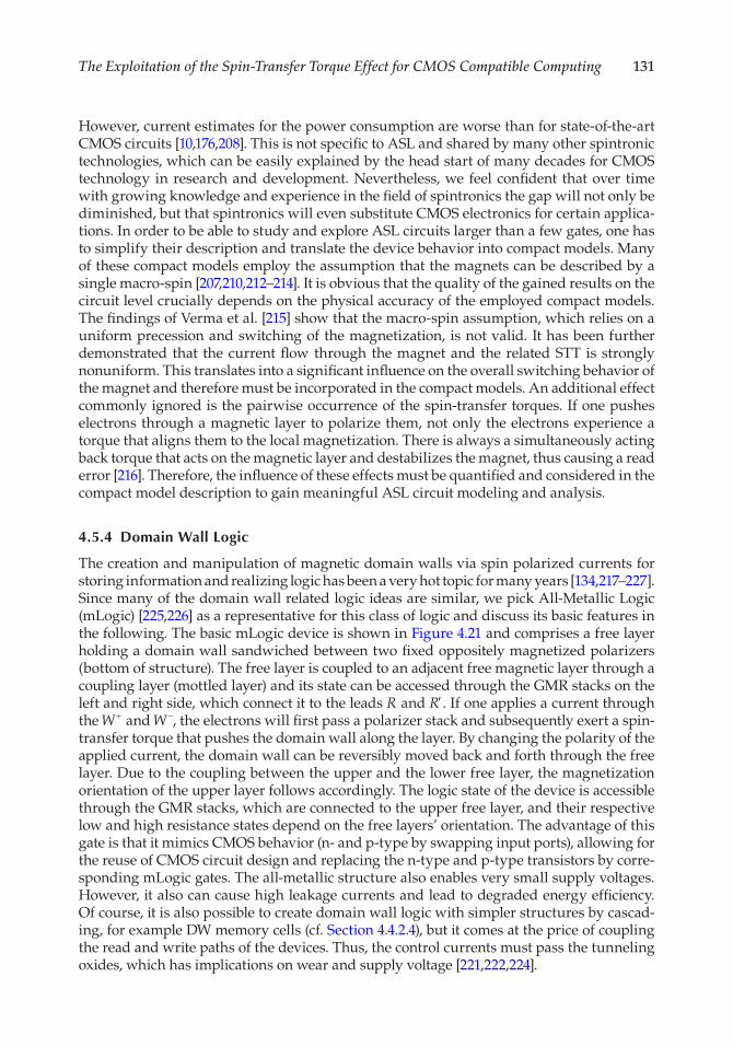
131The Exploitation of the Spin-Transfer Torque Effect for CMOS Compatible Computing
However, current estimates for the power consumption are worse than for state-of-the-art CMOS circuits [10,176,208]. This is not speci�c to ASL and shared by many other spintronic technologies, which can be easily explained by the head start of many decades for CMOS technology in research and development. Nevertheless, we feel con�dent that over time with growing knowledge and experience in the �eld of spintronics the gap will not only be diminished, but that spintronics will even substitute CMOS electronics for certain applica-tions. In order to be able to study and explore ASL circuits larger than a few gates, one has to simplify their description and translate the device behavior into compact models. Many of these compact models employ the assumption that the magnets can be described by a single macro-spin [207,210,212–214]. It is obvious that the quality of the gained results on the circuit level crucially depends on the physical accuracy of the employed compact models. The �ndings of Verma et al. [215] show that the macro-spin assumption, which relies on a uniform precession and switching of the magnetization, is not valid. It has been further demonstrated that the current �ow through the magnet and the related STT is strongly nonuniform. This translates into a signi�cant in�uence on the overall switching behavior of the magnet and therefore must be incorporated in the compact models. An additional effect commonly ignored is the pairwise occurrence of the spin-transfer torques. If one pushes electrons through a magnetic layer to polarize them, not only the electrons experience a torque that aligns them to the local magnetization. There is always a simultaneously acting back torque that acts on the magnetic layer and destabilizes the magnet, thus causing a read error [216]. Therefore, the in�uence of these effects must be quanti�ed and considered in the compact model description to gain meaningful ASL circuit modeling and analysis.
4.5.4 Domain Wall Logic
The creation and manipulation of magnetic domain walls via spin polarized currents for storing information and realizing logic has been a very hot topic for many years [134,217–227]. Since many of the domain wall related logic ideas are similar, we pick All-Metallic Logic (mLogic) [225,226] as a representative for this class of logic and discuss its basic features in the following. The basic mLogic device is shown in Figure 4.21 and comprises a free layer holding a domain wall sandwiched between two �xed oppositely magnetized polarizers (bottom of structure). The free layer is coupled to an adjacent free magnetic layer through a coupling layer (mottled layer) and its state can be accessed through the GMR stacks on the left and right side, which connect it to the leads R and ′R . If one applies a current through the W + and W −, the electrons will �rst pass a polarizer stack and subsequently exert a spin-transfer torque that pushes the domain wall along the layer. By changing the polarity of the applied current, the domain wall can be reversibly moved back and forth through the free layer. Due to the coupling between the upper and the lower free layer, the magnetization orientation of the upper layer follows accordingly. The logic state of the device is accessible through the GMR stacks, which are connected to the upper free layer, and their respective low and high resistance states depend on the free layers’ orientation. The advantage of this gate is that it mimics CMOS behavior (n- and p-type by swapping input ports), allowing for the reuse of CMOS circuit design and replacing the n-type and p-type transistors by corre-sponding mLogic gates. The all-metallic structure also enables very small supply voltages. However, it also can cause high leakage currents and lead to degraded energy ef�ciency. Of course, it is also possible to create domain wall logic with simpler structures by cascad-ing, for example DW memory cells (cf. Section 4.4.2.4), but it comes at the price of coupling the read and write paths of the devices. Thus, the control currents must pass the tunneling oxides, which has implications on wear and supply voltage [221,222,224].
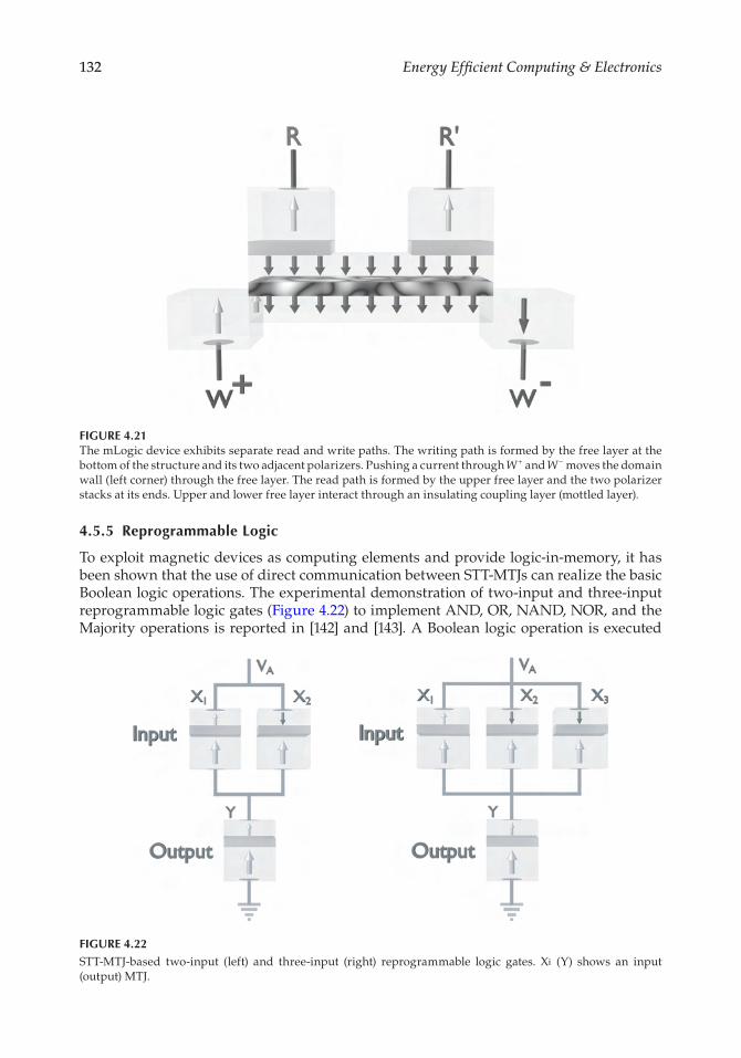
132 Energy Efficient Computing & Electronics
4.5.5 Reprogrammable Logic
To exploit magnetic devices as computing elements and provide logic-in-memory, it has been shown that the use of direct communication between STT-MTJs can realize the basic Boolean logic operations. The experimental demonstration of two-input and three-input reprogrammable logic gates (Figure 4.22) to implement AND, OR, NAND, NOR, and the Majority operations is reported in [142] and [143]. A Boolean logic operation is executed
FIGURE 4.21The mLogic device exhibits separate read and write paths. The writing path is formed by the free layer at the bottom of the structure and its two adjacent polarizers. Pushing a current through W + and W − moves the domain wall (left corner) through the free layer. The read path is formed by the upper free layer and the two polarizer stacks at its ends. Upper and lower free layer interact through an insulating coupling layer (mottled layer).
FIGURE 4.22
STT-MTJ-based two-input (left) and three-input (right) reprogrammable logic gates. Xi (Y) shows an input ( output) MTJ.

133The Exploitation of the Spin-Transfer Torque Effect for CMOS Compatible Computing
in two sequential steps. These steps comprise an appropriate preset operation (parallel or antiparallel state) in the output MTJ. Then a voltage pulse (VA) with a proper amplitude is applied to the gate. Depending on the logic states of the input MTJs (Xi), the preset in the output MTJ (Y), and the voltage level applied to the gate, a conditional switching behavior in the output MTJ is provided, which corresponds to a particular logic operation.
Tables 4.1 and 4.2 illustrate how the AND and OR operation and NAND and NOR opera-tion, respectively, are performed using the two-input reprogrammable gate in two steps. The HRS and the LRS correspond to logical 0 and 1, respectively and the variable xi and y repre-sent the logic state of the input (Xi) and output (Y) MTJs. In order to perform a logic opera-tion, �rst a preset of y = 1 or y = 0 is performed in the output MTJ and then in the following step a proper voltage level (VA < 0 or VA > 0 is applied to the gate to enforce the desired (high-to-low or low-to-high) resistance switching event in the output MTJ, which corresponds to a logic operation (i.e., AND/OR or NAND/NOR). The value of the voltage VA has to be opti-mized to ensure a reliable conditional switching behavior of the output MTJ for any possible input pattern [228]. In fact, this optimization is required for any logic operation to maximize (minimize) the switching probability in the output MTJ (P → 1 or P → 0), when it is a desired (an undesired) switching event in Step 2. One should note that the switching probability of any input MTJ is negligible as the current �owing through the output MTJ splits between the input MTJs, and their currents are below the critical current required for the STT switching. Therefore, the logic state of the input MTJs is left unchanged.
TABLE 4.1
The realized conditional switching behavior is equivalent to the AND and OR operations with a preset of y = 1. Using the two-input reprogrammable gate.
Input Patterns
′y x x←← 1 2AND y x x’ ←← 1 2OR
Step 1 Step 2 Step 1 Step 2
State x1 x2 y ′y y ′y
1 LRS (0) LRS (0) HRS (1) LRS (0) HRS (1) LRS (0)2 LRS (0) HRS (1) HRS (1) LRS (0) HRS (1) HRS (1)3 HRS (1) LRS (0) HRS (1) LRS (0) HRS (1) HRS (1)4 HRS (1) HRS (1) HRS (1) HRS (1) HRS (1) HRS (1)
Desired switching events in the output ( ′y ) are indicated by boldface type.
TABLE 4.2
The realized conditional switching behavior is equivalent to the NAND and NOR operations with a preset of y = 0. Using the two-input reprogrammable gate.
Input Patterns
′y x x←← 1 2NAND ′y x x←← 1 2NOR
Step 1 Step 2 Step 1 Step 2
State x1 x2 y ′y y ′y
1 LRS (0) LRS (0) LRS (0) HRS (1) LRS (0) HRS (1)2 LRS (0) HRS (1) LRS (0) HRS (1) LRS (0) LRS (0)3 HRS (1) LRS (0) LRS (0) HRS (1) LRS (0) LRS (0)4 HRS (1) HRS (1) LRS (0) LRS (0) LRS (0) LRS (0)
Desired switching events in the output ( ′y ) are indicated by boldface type.
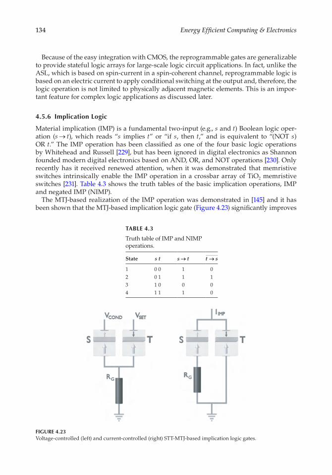
134 Energy Efficient Computing & Electronics
Because of the easy integration with CMOS, the reprogrammable gates are generalizable to provide stateful logic arrays for large-scale logic circuit applications. In fact, unlike the ASL, which is based on spin-current in a spin-coherent channel, reprogrammable logic is based on an electric current to apply conditional switching at the output and, therefore, the logic operation is not limited to physically adjacent magnetic elements. This is an impor-tant feature for complex logic applications as discussed later.
4.5.6 Implication Logic
Material implication (IMP) is a fundamental two-input (e.g., s and t) Boolean logic oper-ation (s t→ ), which reads “s implies t” or “if s, then t,” and is equivalent to “(NOT s) OR t.” The IMP operation has been classi�ed as one of the four basic logic operations by Whitehead and Russell [229], but has been ignored in digital electronics as Shannon founded modern digital electronics based on AND, OR, and NOT operations [230]. Only recently has it received renewed attention, when it was demonstrated that memristive switches intrinsically enable the IMP operation in a crossbar array of TiO2 memristive switches [231]. Table 4.3 shows the truth tables of the basic implication operations, IMP and negated IMP (NIMP).
The MTJ-based realization of the IMP operation was demonstrated in [145] and it has been shown that the MTJ-based implication logic gate (Figure 4.23) signi�cantly improves
TABLE 4.3
Truth table of IMP and NIMP operations.
State s t s t→→ t s→→
1 0 0 1 02 0 1 1 13 1 0 0 04 1 1 1 0
FIGURE 4.23Voltage-controlled (left) and current-controlled (right) STT-MTJ-based implication logic gates.
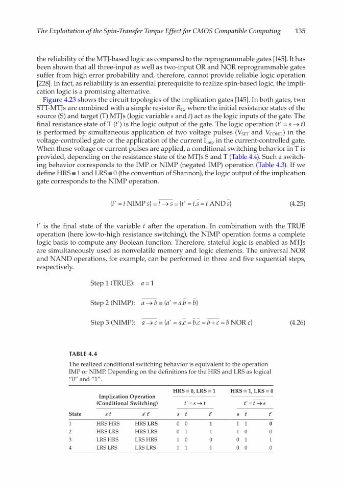
135The Exploitation of the Spin-Transfer Torque Effect for CMOS Compatible Computing
the reliability of the MTJ-based logic as compared to the reprogrammable gates [145]. It has been shown that all three-input as well as two-input OR and NOR reprogrammable gates suffer from high error probability and, therefore, cannot provide reliable logic operation [228]. In fact, as reliability is an essential prerequisite to realize spin-based logic, the impli-cation logic is a promising alternative.
Figure 4.23 shows the circuit topologies of the implication gates [145]. In both gates, two STT-MTJs are combined with a simple resistor RG, where the initial resistance states of the source (S) and target (T) MTJs (logic variable s and t) act as the logic inputs of the gate. The �nal resistance state of T (t’) is the logic output of the gate. The logic operation ( )t’ s t= → is performed by simultaneous application of two voltage pulses (VSET and VCOND) in the voltage-controlled gate or the application of the current Iimp in the current-controlled gate. When these voltage or current pulses are applied, a conditional switching behavior in T is provided, depending on the resistance state of the MTJs S and T (Table 4.4). Such a switch-ing behavior corresponds to the IMP or NIMP (negated IMP) operation (Table 4.3). If we de�ne HRS ≡ 1 and LRS ≡ 0 (the convention of Shannon), the logic output of the implication gate corresponds to the NIMP operation.
{ = } { = . = }t’ t s t s t’ t s t sNIMP AND≡ → ≡ (4.25)
t’ is the �nal state of the variable t after the operation. In combination with the TRUE operation (here low-to-high resistance switching), the NIMP operation forms a complete logic basis to compute any Boolean function. Therefore, stateful logic is enabled as MTJs are simultaneously used as nonvolatile memory and logic elements. The universal NOR and NAND operations, for example, can be performed in three and �ve sequential steps, respectively.
= 1Step 1 (TRUE): a
{ = . = }Step 2 (NIMP): a b a’ a b b→ ≡
{ = . = . = = }Step 3 (NIMP): NORa c a’ a c b c b c b c→ ≡ + (4.26)
TABLE 4.4
The realized conditional switching behavior is equivalent to the operation IMP or NIMP. Depending on the de�nitions for the HRS and LRS as logical “0” and “1”.
Implication Operation (Conditional Switching)
HRS ≡ 0, LRS ≡ 1 HRS ≡ 1, LRS ≡ 0
′t s t== →→ ′t t s== →→
State s t ′s ′t s t ′t s t ′t
1 HRS HRS HRS LRS 0 0 1 1 1 02 HRS LRS HRS LRS 0 1 1 1 0 03 LRS HRS LRS HRS 1 0 0 0 1 14 LRS LRS LRS LRS 1 1 1 0 0 0
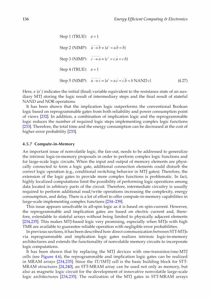
136 Energy Efficient Computing & Electronics
= 1Step 1 (TRUE): a
{ = . = }Step 2 (NIMP): a b a’ a b b→ ≡
{ = . = . }Step 3 (NIMP): c a c’ c a c b→ ≡
= 1Step 4 (TRUE): a
{ = . = . = }Step 5 (NIMP): NANDa c a’ a c c b b c→ ≡ (4.27)
Here, a (a’) indicates the initial (�nal) variable equivalent to the resistance state of an aux-iliary MTJ storing the logic result of intermediary steps and the �nal result of stateful NAND and NOR operations.
It has been shown that the implication logic outperforms the conventional Boolean logic based on reprogrammable gates from both reliability and power consumption point of views [232]. In addition, a combination of implication logic and the reprogrammable logic reduces the number of required logic steps implementing complex logic functions [233]. Therefore, the total time and the energy consumption can be decreased at the cost of higher error probability [233].
4.5.7 Compute-in-Memory
An important issue of nonvolatile logic, the fan-out, needs to be addressed to generalize the intrinsic logic-in-memory proposals in order to perform complex logic functions and for large-scale logic circuits. When the input and output of memory elements are physi-cally connected to form a logic gate, additional connection elements could disturb the correct logic operation (e.g., conditional switching behavior in MTJ gates). Therefore, the extension of the logic gates to provide more complex functions is problematic. In fact, highly localized computations limit the possibility of performing logic operations among data located in arbitrary parts of the circuit. Therefore, intermediate circuitry is usually required to perform additional read/write operations increasing the complexity, energy consumption, and delay. There is a lot of effort to offer compute-in-memory capabilities in large-scale implementing complex functions [234–239].
This issue appears unsolvable in all-spin logic as it is based on spin-current. However, the reprogrammable and implication gates are based on electric current and, there-fore, extendable to stateful arrays without being limited to physically adjacent elements [234,235]. This makes MTJ-based logic very promising, especially when MTJs with high TMR are available to guarantee reliable operation with negligible error probabilities.
In previous sections, it has been described how direct communication between STT-MTJs via reprogrammable and implication logic gates realizes intrinsic logic-in-memory architectures and extends the functionality of nonvolatile memory circuits to incorporate logic computations.
It has been shown that by replacing the MTJ devices with one-transistor/one-MTJ cells (see Figure 4.6), the reprogrammable and implication logic gates can be realized in MRAM arrays [234,235]. Since the 1T/1MTJ cell is the basic building block for STT-MRAM structures [24,240], an STT-MRAM array can be used not only as memory, but also as magnetic logic circuit for the development of innovative nonvolatile large-scale logic architectures [234,235]. The realization of the MTJ gates in STT-MRAM arrays
137The Exploitation of the Spin-Transfer Torque Effect for CMOS Compatible Computing
enables the extension of nonvolatile MRAM from memory to logical computing applica-tions and eliminates the need for sensing ampli�ers and intermediate circuitry as com-pared to other hybrid CMOS/MTJ nonvolatile logic proposals, where the MTJs are used only for nonvolatile storage.
4.6 Spin-Torque Oscillator
Oscillators are important devices ubiquitously needed for many applications [190] and the STT-effect can be exploited to build oscillators. Commonly a spin-torque oscillator (STO) is built as a GMR-pillar or an MTJ. Thus, the GMR or the TMR effect can be used to detect the magnetization oscillation as a high frequency voltage. The precession frequency of STOs is tunable over a wide range of frequencies 5–46 GHz by a DC current as well as by the appli-cation of an external magnetic �eld, which makes them very competitive in comparison to voltage controlled oscillators and Yttrium garnet oscillators [241–244]. They are also very small. STOs are over �fty times smaller than a standard LC-tank voltage controlled oscilla-tor due to the very large required inductor footprint [245]. Their large operation frequency, small size, and low power consumption is very attractive for several microwave-based applications, like broadband oscillators [241–244], fast modulators [246–251], and sensitive �eld/current detectors [252].
There are several ways to categorize STOs. We focus here on their structure and distinguish between nano-contact oscillators, where the current enters though a nano-constriction into an extended magnetic structure and nano-pillar STT oscillators (spin valve or MTJ stack). Nano-contact STOs can be further differentiated by their number of contacts and have been demonstrated for different geometries [253–255]. The nano-pillar STOs can be subdivided into two categories, depending on the magnetization orientation of the free layer: “out-of-plane” with the magnetization perpendicular to the layer and “in-plane” with the magnetization parallel to the layer. Looking at STOs with nano-pillars and in-plane magnetization [256] reveals on one hand high frequency capabilities, but on the other hand the prerequisite of a large external magnetic �eld and low output power levels [257]. In contrast, oscillators with an out-of-plane magnetization of the free layer [258] are able to oscillate without an external magnetic �eld, but suffer under relatively low output power. Additionally, they typically feature lower operation frequencies (≤2 GHz), which limits their potential application as tunable oscillators [257].
Makarov et al. [259,260] proposed a bias-�eld-free STT oscillator with in-plane MgO MTJ, elliptical cross-section, and nonperfect overlap between the free and the �xed layers. This structure exhibits the drawbacks of a weak frequency dependence on the current density and a narrow range of frequencies. A way around these limitations is to use an alternative structure, which employs two MTJ stacks that share a common free layer (cf. Figure 4.24; similar to the NVMFF). This structure allows stable high frequency oscillations without the need of an external magnetic �eld and its operation frequency is widely tunable by varying the current density through the MTJs [261,262]. In [263], it could be demonstrated that in such a structure oscillations up to ≈ 30 GHz are achievable. As further investigations have shown, the structure based on two MTJs with a common shared free layer also exhibits stable oscillations with an out-of-plane magnetization orientation of the free layer [264].
138 Energy Efficient Computing & Electronics
In general, the output power of current STOs is not suf�cient for practical applications yet. Commonly the output power for GMR-based STOs lies in the sub-nW range. CoFeB/MgO/CoFeB based nano-pillar structures achieve higher output power, but still remain in the nW range [265–268]. In order to overcome this problem, the synchronization of several STOs has been proposed [248,254,269–276]. Another solution is to use an external microwave current or �eld to injection lock the synchronization [277–281]. Parametric synchronization with an external microwave �eld frequency close to twice the STO’s free frequency has been reported, a bit more recently [281–284] and bene�ts from the advan-tage that the measurement is not interfered by the external signal. First experimental observation of parametric excitation in a nano-contact STO at cryogenic temperatures and an excitation frequency of twice the STO’s free frequency was achieved by a separately manufactured strip line on top of the STO [285]. Bortolotti et al. [286] were able to para-metrically excite vortex gyration by passing a microwave current through a vortex-based MTJ-STO with a suf�cing Ørsted �eld strength at room temperature. A very encouraging result was shown by Sani et al. [254] in 2013. They were able to mutually synchronize three nano-contact STOs. Nevertheless, even under ideal conditions the parametric exci-tation only shows imperfect locking and the output power as well as the phase noise need further improvement [287].
The above mentioned STOs exploit magnetically hard layers to polarize the electrons before they interact with the free layer to drive precessions. But it is also possible to take advantage of the spin Hall effect for the polarization of the electrons to build spin Hall nano-oscillators (SHNOs). An SHNO comprises a nonmagnetic layer with a strong spin-orbit coupling adjacent to a magnetic layer. These devices are able to create micro-wave signals in the range of 2–10 GHz, which is appealing for applications in the tele-communication domain. These SHNOs work with pure spin signals (cf. Section 4.2.3), only require little power, operate in a wide range of frequencies, and are rather small (≤5 μm) in comparison to state-of-the-art technologies. Several SHNO devices in a vari-ety of geometries have been manufactured and their operation was properly demon-strated, such as a disk with triangular contacts (nano-gap) [288,289], a nano-wire [290], and a nano-constriction [291]. It has been demonstrated that relatively large power and small auto-oscillation linewidth are possible for a localized spin current injection at
FIGURE 4.24This structure exploits one MTJ for driving the oscillations, while the other prevents switching and relaxation into a stable state (opposite current direction). This way large stable oscillations of the common free layer can be not only sustained, but steered over a wide frequency range.
139The Exploitation of the Spin-Transfer Torque Effect for CMOS Compatible Computing
cryogenic temperatures in 2013 [288]. Unfortunately, both features decrease considerably at elevated temperatures due to the availability of additional modes and the arising ther-mal mode hopping [291]. These problems can be avoided by deliberately exciting a single mode; that is, by adjusting the geometric area of the auto-oscillation zone. One would intuitively expect that the auto-oscillation area is correlated to the experimental setup, like the spin injection geometry, but as it turns out the control of the auto-oscillation characteristics is rather tricky [292]. The local injection of a spin signal into a continuous magnetic �lm causes the spontaneous excitation of the bullet auto-oscillation mode [293] and the dimensions of the “bullet” is governed by nonlinear self-localization effects and not the spin injection area [289,294].
4.7 Applications
In this �nal section we highlight a few showcases for spintronic computing, which are likely to be commercialized in the next few years.
4.7.1 Random Number Generator
Since the magnetization of MTJs experiences thermal excitations, their switching shows stochastic behavior and the switching probability of MTJs is governed by the applied cur-rent amplitude. This is commonly considered as an effect that has to be controlled by care-ful circuit design, but one can make a virtue out of necessity by exploiting it for the physical realization of a random number generator [295]. In 2013, a �rst spin-based random-number generator (spin dice) was built by employing a conventional in-plane MTJ and a current adjusted to achieve 50% switching probability [72]. Unfortunately, in-plane MTJs suffer of a rather small magnetic �eld range for bistable states and demand high switching current densities, which caused problems in the practical realization of the spin dice [296]. The next generation utilizes MTJs with perpendicular free layer and a perpendicular synthetic antiferromagnetic bottom reference layer [295,296]. Besides the well known random num-ber generator applications, like Monte Carlo simulations and cryptography, they can also be used to improve analog-to-digital information conversion systems for low energy appli-cations. Lee et al. [297] proposed a very interesting voltage-controlled stochastic oscillator for event-driven random sampling. Due to the exploitation of a VCMA and their deliber-ately reduced thermal barrier, they are able to reduce the power consumption by more than three times and improve the area ef�ciency even by a factor of 20 in comparison to the state-of-the-art.
4.7.2 Ternary Content-Addressable Memory
Content addressable memory (CAM) is the kind of technology that people use every day, but commonly are completely unaware of its existence. Even more, modern databases and search engines, like Google, could not offer high-speed access to data without them. In contrast to RAM, where the user sends an address to the RAM and gets a data word in return, CAMs get a data word from the user, search their entire memory for the data word and, if such entries exist, return a list of addresses where the data word is stored [298]. These memories are designed in a way that they can search their entire memory within
140 Energy Efficient Computing & Electronics
one operation, which makes them very fast but at the same time expensive. The added search capability is realized by additional comparison circuitry in each memory cell, which causes a high power consumption and a considerably increased memory cell foot-print. A ternary CAM (TCAM) extends the functionality of binary CAMs (BCAMs) by adding a third search option “X”—do not care, which gives more freedom for search que-ries but adds additional complexity to the circuit design [299]. The combination of rising demand for (T)CAMs together with their high energy consumption and large layout foot-print makes them very attractive candidates for spintronic complementation. For instance, Govindaraj et al. [300] proposed a 6T 2 STT-MTJ-based NOR-TCAM in 2015 and lately another 9T 2 STT-MTJ based NAND TCAM in 2017 [301]. Considering that a typical CMOS only TCAM cell exhibits 16 transistors, this is a big step forward with respect to integra-tion density and dissipated power. There are TCAMs with smaller memory cell size, like 4T-2MTJ TCAM [302], 3T-2DW BCAM [303], or even 2T-2MTJs [304]. They all feature signi�-cantly smaller memory cells and offer zero standby power, but depending on the applica-tion scenario and the overhead complexity one is able to afford, one or another of these designs will prevail [300,301].
4.7.3 Spin-Transfer Torque Compute-in-Memory (STT-CiM)
One very recent and interesting proposal for a STT-based Compute-in-Memory design was presented by Jain et al. [305]. They suggest to take advantage of the resistive nature of the STT-MRAM cells to perform a range of arithmetic, bitwise, and complex vector operations. The trick is to enable multiple word lines simultaneously and sense the effective resistance of all enabled cells in each bit-line in order to directly perform logic functions depen-dent on the values stored in the cells. Such a scheme is not feasible in SRAMs, because it would cause short circuit paths, but, since the STT-MRAM cells are intrinsically resistors, this problem does not appear. This idea is not new (Section 4.5.7), but the implementation simultaneously addresses process variation issues and allows arithmetic and complex vec-tor operations without modifying either the bit-cell or the data array. The bundle of adjust-ments on different levels (sensing scheme, error correction scheme, and extension of the instruction set) cumulates in an average 4× performance improvement and simultaneous memory system energy reduction.
4.8 Conclusion and Outlook
In this chapter, we tried to give an overview about the many facets of CMOS compatible spintronics and its importance for future beyond Von Neumann computing. Especially STT-switched MTJs have not only become so mature that off-the-shelf MRAM is already available, but the technology as a whole including the process know-how reached a level that we are con�dent that �rst CMOS MTJ hybrids for logic applications will be brought to market very soon. However, MTJs of course also have issues like the still rather high switching currents, reduction of damping, increased thermal stability, and device vari-ability. There are ideas to circumvent (some of) these problems via the spin Hall effect, domain wall motion, or voltage controlled magnetic anisotropies. But domain wall-based MRAM and spin Hall MRAM are by nature three terminal devices and, therefore, require more space, while the voltage controlled magnetic anisotropy coef�cient needs a boost
141The Exploitation of the Spin-Transfer Torque Effect for CMOS Compatible Computing
to make it compatible with advanced CMOS transistors. STT oscillators are an essential building block for digital electronics and show great potential due to their large operation frequencies, small size, and low power consumption. Currently, they suffer under too low output power for many applications, but there are niches where they already can shine like in STO-based random number generators and analog-to-digital information conversion systems for low energy applications.
Overall one can see a gradual evolution on all levels (materials, processing, devices, cir-cuits, and architectures). This evolution drove the introduction of STT-MRAM into market and will also lead to �rst spintronic logic and later beyond Von Neumann products. Most likely, this will happen in high performance computing and database hardware, where reduced cooling power and less power consumption immediately brings a big advantage in operating expenses for high performance computation clusters and big server farms. TCAMs with their rather big and complex memory cells as well as their high power dis-sipation in combination with their crucial role in modern data base applications are perfect replacement candidates. Also FPGAs have a high potential to boost their performance with spintronic logic and will help to familiarize the current generation of developers and engineers with the next generations spintronic technology. FPGAs are very important due to their widespread application in aerospace, medical electronics, application-speci�c inte-gratet circuit (ASIC) prototyping, digital signal processing, image processing, consumer electronics, high performance computing, scienti�c instruments, data mining, and many more. They also open up the next step towards the huge system-on-chip market. More dis-ruptive approaches try to draw from the unique advantages of spintronics and break up the CMOS dominance. For example, ASL or STT logic will take off later, when the CMOS MTJ hybrid logic ecosystem has been established and the companies as well as the market are ready for the next more powerful technology generation. In summary, we can see that spintronics managed to become mature enough for �rst real products, like STT-MRAM, and we are con�dent that it will not stop there and a plethora of nonvolatile spin-based logic is going to appear within the next 5–10 years on the market.
Acknowledgment
This work is supported by the European Research Council through the grant #692653 NOVOFLOP. B. Gunnar Malm wants to acknowledge professor Johan Åkerman and the Applied Spintronics Group at KTH. Special thanks go to Anders Eklund, Sohrab Sani, Stefano Bonetti, and Sunjae Chung.
References
1. D. Shum, D. Houssameddine, S. T. Woo, Y. S. You, J. Wong, K. W. Wong, C. C. Wang et al. CMOS-embedded STT-MRAM arrays in 2x nm nodes for GP-MCU applications. In 2017 Symposium on VLSI Technology, pages T208–T209, 2017.
2. L. Thomas, G. Jan, J. Zhu, H. Liu, Y.-J. Lee, S. Le, R.-Y. Tong et al. Perpendicular spin transfer torque magnetic random access memories with high spin torque ef�ciency and thermal stabil-ity for embedded applications. Journal of Applied Physics, 115(17):172615, 2014.
142 Energy Efficient Computing & Electronics
3. S. Natarajan, M. Agostinelli, S. Akbar, M. Bost, A. Bowonder, V. Chikarmane, S. Chouksey et al. A 14nm logic technology featuring 2nd-generation FinFET, air-gapped interconnects, self-aligned double patterning and a 0.0588
m2 SRAM cell size. In IEEE International Electron Devices Meeting (IEDM), pages 3.7.1–3.7.3, 2014.
4. Intel’s 10 nm technology. https://newsroom.intel.com/newsroom/wp-content/uploads/sites/11/2017/03/10-nm-technology-fact-sheet.pdf. Accessed: July 17, 2017.
5. Samung Electronics 10 nm ramp-up. https://news.samsung.com/global/samsung-electronics-on-track-for-10nm-�nfet-process-technology-production-ramp-up. Accessed: July 17, 2017.
6. TSMC’s 10 nm process for Apple’s A10X fusion chip. http://www.idownloadblog.com/2017/06/30/apples-latest-a10x-fusion-chip-is-built-using-tsmcs-10nm-process/. Accessed: July 17, 2017.
7. B. Doris, M. Ieong, T. Kanarsky, Y. Zhang, R. A. Roy, O. Dokumaci, Z. Ren et al. Extreme scal-ing with ultra-thin Si channel MOSFETs. In IEEE International Electron Devices Meeting (IEDM), pages 267–270, 2002.
8. I. Žutić, J. Fabian, and S.D. Sarma. Spintronics: Fundamentals and applications. Reviews of Modern Physics, 76(2):323–410, 2004.
9. J. Fabian, A. Matos-Abiague, C. Ertler, P. Stano, and I. Žutić. Semiconductor spintronics. Acta Physica Slovaca, 57(4–5):565–907, 2007.
10. J. Kim, A. Paul, P. A. Crowell, S. J. Koester, S. S. Sapatnekar, J. P. Wang, and C. H. Kim. Spin-based computing: Device concepts, current status, and a case study on a high-performance microprocessor. In Proceedings of the IEEE, Vol. 103, pages 106–130, 2015.
11. G. Schmidt, D. Ferrand, L. W. Molenkamp, A.T. Filip, and B.J. Van Wees. Fundamental obstacle for electrical spin injection from a ferromagnetic metal into a diffusive semiconductor. Physical Review B, 62(8):R4790–R4793, 2000.
12. E. I. Rashba. Theory of electrical spin injection: Tunnel contacts as a solution of the conductiv-ity mismatch problem. Physical Review B - Condensed Matter and Materials Physics, 62(24):R16267–R16270, 2000.
13. O. M. J. Van’t Erve, A. L. Friedman, E. Cobas, C. H. Li, J. T. Robinson, and B. T. Jonker. Low-resistance spin injection into silicon using graphene tunnel barriers. Nature Nanotechnology, 7(11):737–742, 2012.
14. R. Jansen. Silicon spintronics. Nature Materials, 11(5):400–408, 2012. 15. B. Huang, D. J. Monsma, and I. Appelbaum. Coherent spin transport through a 350 micron
thick silicon wafer. Physical Review Letters, 99:177209, 2007. 16. J. Li and I. Appelbaum. Lateral spin transport through bulk silicon. Applied Physics Letters,
100(16):162408, 2012. 17. V. Sverdlov. Strain-Induced Effects in Advanced MOSFETs. Computational Microelectronics.
Springer-Verlag, Wien, Austria, 2011. 18. V. Sverdlov and S. Selberherr. Silicon spintronics: Progress and challenges. Physics Reports,
585:1–40, 2015. 19. P. Chuang, S.-C. Ho, L. W. Smith, F. S�gakis, M. Pepper, C.-H. Chen, J.-C. Fan et al. All-electric
all-semiconductor spin �eld-effect transistors. Nature Nanotechnology, 10(1):35–39, 2015. 20. T. Tahara, H. Koike, M. Kameno, T. Sasaki, Y. Ando, K. Tanaka, S. Miwa, Y. Suzuki, and
M. Shiraishi. Room-temperature operation of Si spin MOSFET with high on/off spin signal ratio. Applied Physics Express, 8(11):113004, 2015.
21. A. Makarov, T. Windbacher, V. Sverdlov, and S. Selberherr. CMOS-compatible spintronic devices: A review. Semiconductor Science and Technology, 31(11):113006, 2016.
22. A. Makarov, V. Sverdlov, and S. Selberherr. Emerging memory technologies: Trends, chal-lenges, and modeling methods. Microelectronics Reliability, 52(4):628–634, 2012.
23. S. A. Wolf, J. Lu, M. R. Stan, E. Chen, and D. M. Treger. The promise of nanomagnetics and spintronics for future logic and universal memory. In Proceedings of the IEEE, Vol. 98, pages 2155–2168, 2010.
24. C. Augustine, N. Mojumder, X. Fong, H. Choday, S. P. Park, and K. Roy. STT-MRAMs for future universal memories: Perspective and prospective. In Proceedings of the International Conference on Microelectronics (MIEL), pages 349–355, 2012.
143The Exploitation of the Spin-Transfer Torque Effect for CMOS Compatible Computing
25. W. Zhao and G. Prenat. Spintronics-Based Computing. Springer International Publishing, 2015. 26. M. N. Baibich, J. M. Broto, A. Fert, F. Nguyen Van Dau, F. Petroff, P. Etienne, G. Creuzet,
A. Friederich, and J. Chazelas. Giant magnetoresistance of (001)Fe/(001)Cr magnetic superlattices. Physical Review Letters, 61:2472–2475, 1988.
27. G. Binasch, P. Grünberg, F. Saurenbach, and W. Zinn. Enhanced magnetoresistance in layered magnetic structures with antiferromagnetic interlayer exchange. Physical Review B, 39:4828–4830, 1989.
28. P. Zahn and I. Mertig. Enhanced magnetoresistance. In Handbook of Magnetism and Advanced Magnetic Materials, Vol. 1, Fundamentals and Theory. John Wiley & Sons, Hoboken, NJ, 2007.
29. G. A. Prinz. Spin-polarized transport. Physics Today, 48(4):58–63, 1995. 30. C. Chappert, A. Fert, and F. Nguyen Van Dau. The emergence of spin electronics in data stor-
age. Nature Materials, 6(11):813–823, 2007. 31. S. Tehrani, Jon M. Slaughter, M. DeHerrera, B. N. Engel, N. D. Rizzo, J. Salter et al.
Magnetoresistive random access memory using magnetic tunnel junctions. In Proceedings of the IEEE, Vol. 91, pages 703–714, 2003.
32. M. Julliere. Tunneling between ferromagnetic �lms. Physics Letters A, 54(3):225–226, 1975. 33. H. Imamura and S. Maekawa. Theory of spin-dependent tunneling. In Handbook of Magnetism
and Advanced Magnetic Materials. John Wiley & Sons, Hoboken, NJ, 2007. 34. A. V. Khvalkovskiy, D. Apalkov, S. Watts, R. Chepulskii, R.S. Beach, A. Ong, X. Tang et al. Basic
principles of STT-MRAM cell operation in memory arrays. Journal of Physics D: Applied Physics, 46(8):074001, 2013.
35. J. S. Moodera, Lisa R. Kinder, Terrilyn M. Wong, and R. Meservey. Large magnetoresistance at room temperature in ferromagnetic thin �lm tunnel junctions. Physical Review Letters, 74:3273–3276, 1995.
36. T. Miyazaki and N. Tezuka. Giant magnetic tunneling effect in Fe/Al2O3/Fe junction. Journal of Magnetism and Magnetic Materials, 139(3):L231–L234, 1995.
37. D. Wang, C. Nordman, J.M. Daughton, Z. Qian, and J. Fink. 70% TMR at room temperature for SDT sandwich junctions with CoFeB as free and reference layers. IEEE Transactions on Magnetics, 40(4):2269–2271, 2004.
38. W. H. Butler, X.-G. Zhang, T. C. Schulthess, and J. M. MacLaren. Spin-dependent tunneling conductance of Fe/MgO/Fe sandwiches. Physical Review B, 63:054416, 2001.
39. J. Mathon and A. Umerski. Theory of tunneling magnetoresistance of an epitaxial Fe/MgO/Fe(001) junction. Physical Review B, 63:220403, 2001.
40. M. Bowen, V. Cros, F. Petroff, A. Fert, C. Martínez Boubeta, J. L. Costa-Krämer, J. V. Anguita et al. Large magnetoresistance in Fe/MgO/FeCo(001) epitaxial tunnel junctions on GaAs(001). Applied Physics Letters, 79(11):1655–1657, 2001.
41. S. S. P. Parkin, C. Kaiser, A. Panchula, P. M. Rice, B. Hughes, M. Samant, and S.-H. Yang. Giant tunnelling magnetoresistance at room temperature with MgO(100) tunnel barriers. Nature Materials, 3(12):862–867, 2004.
42. S. Yuasa, T. Nagahama, A. Fukushima, Y. Suzuki, and K. Ando. Giant room-temperature magnetoresistance in single-crystal Fe/MgO/Fe magnetic tunnel junctions. Nature Materials, 3(12):868–871, 2004.
43. S. Yuasa, A. Fukushima, H. Kubota, Y. Suzuki, and K. Ando. Giant tunneling magnetoresis-tance up to 410% at room temperature in fully epitaxial Co/MgO/Co magnetic tunnel junc-tions with BCC Co(001) electrodes. Applied Physics Letters, 89(4):042505, 2006.
44. S. Ikeda, J. Hayakawa, Y. Ashizawa, Y. M. Lee, K. Miura, H. Hasegawa, M. Tsunoda, F. Matsukura, and H. Ohno. Tunnel magnetoresistance of 604% at 300K by suppression of Ta diffusion in CoFeB/MgO/CoFeB pseudo-spin-valves annealed at high temperature. Applied Physics Letters, 93(8):082508, 2008.
45. R. Sbiaa, H. Meng, and S. N. Piramanayagam. Materials with perpendicular magnetic anisotropy for magnetic random access memory. Physica Status Solidi - Rapid Research Letters, 5(12):413–419, 2011.
46. J. C. Slonczewski. Current-driven excitation of magnetic multilayers. Journal of Magnetism and Magnetic Materials, 159(1–2):L1–L7, 1996.
144 Energy Efficient Computing & Electronics
47. L. Berger. Emission of spin waves by a magnetic multilayer traversed by a current. Physical Review B, 54:9353–9358, 1996.
48. J. Grollier, V. Cros, A. Hamzic, J. M. George, H. Jaffrès, A. Fert, G. Faini, J. Ben Youssef, and H. Legall. Spin-polarized current induced switching in Co/Cu/Co pillars. Applied Physics Letters, 78(23):3663–3665, 2001.
49. J. A. Katine, F. J. Albert, R. A. Buhrman, E. B. Myers, and D. C. Ralph. Current-driven magneti-zation reversal and spin-wave excitations in Co/Cu/Co pillars. Physical Review Letters, 84:3149–3152, 2000.
50. E. B. Myers, D. C. Ralph, J. A. Katine, R. N. Louie, and R. A. Buhrman. Current-induced switch-ing of domains in magnetic multilayer devices. Science, 285(5429):867–870, 1999.
51. J.Z Sun. Current-driven magnetic switching in manganite trilayer junctions. Journal of Magnetism and Magnetic Materials, 202(1):157–162, 1999.
52. M. Tsoi, A. G. M. Jansen, J. Bass, W.-C. Chiang, M. Seck, V. Tsoi, and P. Wyder. Excitation of a magnetic multilayer by an electric current. Physical Review Letters, 80:4281–4284, 1998.
53. Y. Huai, F. Albert, P. Nguyen, M. Pakala, and T. Valet. Observation of spin-transfer switching in deep submicron-sized and low-resistance magnetic tunnel junctions. Applied Physics Letters, 84(16):3118–3120, 2004.
54. Z. Diao, D. Apalkov, M. Pakala, Y. Ding, A. Panchula, and Y. Huai. Spin transfer switching and spin polarization in magnetic tunnel junctions with MgO and AlOx barriers. Applied Physics Letters, 87(23):232502, 2005.
55. M. I. Dyakonov and V. I. Perel. Spin relaxation of conduction electrons in noncentrosymetric semiconductors. Fizika Tverdogo Tela, 13:1382–1397, 1971.
56. E. L. Ivchenko, G. E. Pikus, I. I. Farbshtein, V. A. Shalygin, A. V. Shturbin, and L. E. Vorob’ev. Optical activity in tellurium induced by a current. JETP Letters, 29(8):441–444, 1979.
57. Y. Kato, R. C. Myers, A. C. Gossard, and D. D. Awschalom. Observation of the spin Hall effect in semiconductors. Science, 306(5703):1910–1913, 2004.
58. S. O. Valenzuela and M. Tinkham. Direct electronic measurement of the spin Hall effect. Nature, 442(7099):176–179, 2006.
59. J. E. Hirsch. Spin Hall effect. Physical Review Letters, 83:1834–1837, 1999. 60. J. Wunderlich, B. Kaestner, J. Sinova, and T. Jungwirth. Experimental observation of the spin-
Hall effect in a two-dimensional spin-orbit coupled semiconductor system. Physical Review Letters, 94:047204, 2005.
61. T. Kimura, Y. Otani, T. Sato, S. Takahashi, and S. Maekawa. Room-temperature reversible spin Hall effect. Physical Review Letters, 98:156601, 2007.
62. P. K. Amiri, J. G. Alzate, X. Q. Cai, F. Ebrahimi, Q. Hu, K. Wong, C. Grèzes et al. Electric-�eld-controlled magnetoelectric RAM: Progress, challenges, and scaling. IEEE Transactions on Magnetics, 51(11):1–7, 2015.
63. M. Weisheit, S. Fähler, A. Marty, Y. Souche, C. Poinsignon, and D. Givord. Electric �eld-induced modi�cation of magnetism in thin-�lm ferromagnets. Science, 315(5810):349–351, 2007.
64. T. Maruyama, Y. Shiota, T. Nozaki, K. Ohta, N. Toda, M. Mizuguchi, A.A. Tulapurkar et al. Large voltage-induced magnetic anisotropy change in a few atomic layers of iron. Nature Nanotechnology, 4(3):158–161, 2009.
65. Y. Shiota, T. Maruyama, T. Nozaki, T. Shinjo, M. Shiraishi, and Y. Suzuki. Voltage-assisted magnetization switching in ultrathin Fe80Co20 alloy layers. Applied Physics Express, 2(6):063001, 2009.
66. T. Nozaki, H. Arai, K. Yakushiji, S. Tamaru, H. Kubota, H. Imamura, A. Fukushima, and S. Yuasa. Magnetization switching assisted by high-frequency-voltage-induced ferromagnetic resonance. Applied Physics Express, 7(7):073002, 2014.
67. X. Li, K. Fitzell, D. Wu, C. T. Karaba, A. Buditama, G. Yu, K. L. Wong et al. Enhancement of voltage-controlled magnetic anisotropy through precise control of Mg insertion thickness at CoFeB|MgO interface. Applied Physics Letters, 110(5):052401, 2017.
68. K. L. Wang, J. G. Alzate, and P. K. Amiri. Low-power non-volatile spintronic memory: STT-RAM and beyond. Journal of Physics D: Applied Physics, 46(7):074003, 2013.

145The Exploitation of the Spin-Transfer Torque Effect for CMOS Compatible Computing
69. S. E. Barnes, J. Ieda, and S. Maekawa. Rashba spin-orbit anisotropy and the electric �eld con-trol of magnetism. Scientific Reports, 4:4105, 2014.
70. W. Kim, J. H. Jeong, Y. Kim, W. C. Lim, J. H. Kim, J. H. Park, H. J. Shin et al. Extended scalabil-ity of perpendicular STT-MRAM towards sub-20nm MTJ node. In IEEE International Electron Devices Meeting (IEDM), pages 24.1.1–24.1.4, 2011.
71. B. Dieny and M. Chshiev. Perpendicular magnetic anisotropy at transition metal/oxide inter-faces and applications. Reviews of Modern Physics, 89:025008, 2017.
72. S. Yuasa, A. Fukushima, K. Yakushiji, T. Nozaki, M. Konoto, H. Maehara, H. Kubota et al. Future prospects of MRAM technologies. In IEEE International Electron Devices Meeting (IEDM), pages 3.1.1–3.1.4, 2013.
73. S. Wang, H. Lee, F. Ebrahimi, P. K. Amiri, K. L. Wang, and P. Gupta. Comparative evaluation of spin-transfer-torque and magnetoelectric random access memory. IEEE Journal on Emerging and Selected Topics in Circuits and Systems, 6(2):134–145, 2016.
74. S. W. Chung, T. Kishi, J. W. Park, M. Yoshikawa, K. S. Park, T. Nagase, K. Sunouchi et al. 4Gbit density STT-MRAM using perpendicular MTJ realized with compact cell structure. In IEEE International Electron Devices Meeting (IEDM), pages 27.1.1–27.1.4, 2016.
75. D. Apalkov, A. Khvalkovskiy, S. Watts, V. Nikitin, X. Tang, D. Lottis, K. Moon et al. Spin-transfer torque magnetic random access memory (STT-MRAM). Journal of Emerging Technology in Computer System, 9(2):13:1–13:35, 2013.
76. Y. Lu, X. Li, S. H. KANG, and S. Gu. Self-aligned top contact for MRAM fabrication, 2016. EP Patent App. 3095144.
77. M. Piquemal-Banci, R. Galceran, M.-B. Martin, F. Godel, A. Anane, F. Petroff, B. Dlubak, and P. Seneor. 2D-MTJs: Introducing 2D materials in magnetic tunnel junctions. Journal of Physics D: Applied Physics, 50(20):203002, 2017.
78. E. Cobas, A. L. Friedman, O. M. J. van’t Erve, J. T. Robinson, and B. T. Jonker. Graphene as a tunnel barrier: Graphene-based magnetic tunnel junctions. Nano Letters, 12(6):3000–3004, 2012.
79. M.-B. Martin, B. Dlubak, R. S. Weatherup, H. Yang, C. Deranlot, K. Bouzehouane, F. Petroff et al. Sub-nanometer atomic layer deposition for spintronics in magnetic tunnel junctions based on graphene spin-�ltering membranes. ACS Nano, 8(8):7890–7895, 2014.
80. M. Gajek, J. J. Nowak, J. Z. Sun, P. L. Trouilloud, E. J. O’Sullivan, D. W. Abraham, M. C. Gaidis et al. Spin torque switching of 20nm magnetic tunnel junctions with perpendicular anisot-ropy. Applied Physics Letters, 100(13):132408, 2012.
81. H. Sato, E. C. I. Enobio, M. Yamanouchi, S. Ikeda, S. Fukami, S. Kanai, F. Matsukura, and H. Ohno. Properties of magnetic tunnel junctions with a MgO/CoFeB/Ta/CoFeB/MgO record-ing structure down to junction diameter of 11nm. Applied Physics Letters, 105(6):062403, 2014.
82. S. Tan, T. KIM, W. Yang, J. Marks, and T. Lill. Dry plasma etch method to pattern MRAM stack, 2016. US Patent App. 20160308112.
83. N. Sakimura, T. Sugibayashi, R. Nebashi, and N. Kasai. Nonvolatile magnetic �ip-�op for standby-power-free SoCs. In 2008 IEEE Custom Integrated Circuits Conference, pages 355–358, 2008.
84. Y. J. Song, J. H. Lee, H. C. Shin, K. H. Lee, K. Suh, J. R. Kang, S. S. Pyo et al. Highly functional and reliable 8Mb STT-MRAM embedded in 28nm logic. In IEEE International Electron Devices Meeting (IEDM), pages 27.2.1–27.2.4, 2016.
85. J. M. Slaughter, N. D. Rizzo, J. Janesky, R. Whig, F. B. Mancoff, D. Houssameddine, J. J. Sun et al. High density ST-MRAM technology. In IEEE International Electron Devices Meeting (IEDM), pages 29.3.1–29.3.4, 2012.
86. J. J. Kan, C. Park, C. Ching, J. Ahn, L. Xue, R. Wang, A. Kontos et al. Systematic validation of 2x nm diameter perpendicular MTJ arrays and MgO barrier for sub-10 nm embedded STT-MRAM with practically unlimited endurance. In IEEE International Electron Devices Meeting (IEDM), pages 27.4.1–27.4.4, 2016.
87. M. C. Gaidis. Magnetoresistive Random Access Memory. Wiley-VCH Verlag GmbH & Co. KGaA, 2010. 88. J. R. Black. Mass transport of aluminum by momentum exchange with conducting electrons.
In 2005 IEEE International Reliability Physics Symposium, 2005. Proceedings. 43rd Annual, pages 1–6, 2005.
146 Energy Efficient Computing & Electronics
89. K. Itoh. VLSI Memory Chip Design. Advanced Microelectronics. Springer-Verlag, Berlin, Germany, 2001.
90. A. Chen. A review of emerging non-volatile memory (NVM) technologies and applications. Solid-State Electronics, 125:25–38, 2016.
91. T. Endoh, H. Koike, S. Ikeda, and H. Ohno. An overview of nonvolatile emerging memories – Spintronics for working memories. IEEE Journal on Merging and Selected Topics in Circuits and Systems, 6(2):109–119, 2016.
92. J. J. Kan, C. Park, C. Ching, J. Ahn, Y. Xie, M. Pakala, and S. H. Kang. A study on practically unlimited endurance of STT-MRAM. In IEEE Transactions on Electron Devices (IEDM), Vol. 64, pages 3639–3646, 2017.
93. E. Kitagawa, S. Fujita, K. Nomura, H. Noguchi, K. Abe, K. Ikegami, T. Daibou et al. Impact of ultra low power and fast write operation of advaced perpendicular MTJ on power reduction for high-performance mobile CPU. In IEEE International Electron Devices Meeting (IEDM), pages 29.4.1–29.4.4, 2012.
94. T. Ohsawa, S. Miura, H. Honjo, S. Ikeda, T. Hanyu, H. Ohno, and Endoh T. A 500ps/8.5ns array read/write latency 1Mb twin 1T1MTJ STT-MRAM designed in 90nm CMOS/40nm MTJ process with novel positive feedback S/A circuit. In 2014 International Conference on Solid State Devices and Materials, pages 458–459, 2014.
95. Everspin’s STT technology. https://www.everspin.com/ddr3-dram-compatible-mram-spin-torque-technology-0. Accessed: September 7, 2017.
96. D. Apalkov, B. Dieny, and J. M. Slaughter. Magnetoresistive Random Access Memory. Proceedings of the IEEE, 104(10):1796–1830, 2016.
97. Y. M. Lee, J. Hayakawa, S. Ikeda, F. Matsukura, and H. Ohno. Effect of electrode composition on the tunnel magnetoresistance of pseudo-spin-valve magnetic tunnel junction with a MgO tunnel barrier. Applied Physics Letters, 90:212507, 2007.
98. D. Apalkov, S. Watts, A. Driskill-Smith, E. Chen, Z. Diao, and V. Nikitin. Comparison of scaling of in-plane and perpendicular spin transfer switching technologies by micromagnetic simula-tion. IEEE Transactions on Magnetics, 46:2240–2243, 2010.
99. E. Chen, D. Apalkov, Z. Diao, A. Driskill-Smith, D. Druist, D. Lottis, V. Nikitin et al. Advances and future prospects of spin-transfer torque random access memory. IEEE Transactions on Magnetics, 46(6):1873–1878, 2010.
100. B. D. Cullity and C. D. Graham. Introduction to Magnetic Materials. John Wiley & Sons, Hoboken, NJ, 2009.
101. S. Mangin, D. Ravelosona, J. A. Katine, M. J. Carey, B. D. Terris, and E. E. Fullerton. Current-induced magnetization reversal in nanopillars with perpendicular anisotropy. Nature Materials, 5:210–215, 2006.
102. T. Seki, S. Mitani, K. Yakushiji, and K. Takanashi. Magnetization switching in nanopillars with FePt alloys by spin-polarized current. Journal of Applied Physics, 5:08G521, 2006.
103. D. C. Worledge, G. Hu, D. W. Abraham, J. Z. Sun, P. L. Trouilloud, J. Nowak, S. Brown, M. C. Gaidis, E. J. O’Sullivan, and R. P. Robertazzi. Spin torque switching of perpendicular Ta|CoFeB|MgO-based magnetic tunnel junctions. Applied Physics Letters, 98:022501, 2011.
104. H. Sato, M. Yamanouchi, K. Miura, S. Ikeda, H. D. Gan, K. Mizunuma, R. Koizumi, F. Matsukura, and H. Ohno. Junction size effect on switching current and thermal stability in CoFeB/MgO perpendicular magnetic tunnel junctions. Applied Physics Letters, 99:042501, 2011.
105. J. Nogués and I. K. Schuller. Exchange bias. Journal of Magnetism and Magnetic Materials, 192:203–232, 1999.
106. D. M. Edwards, J. Mathon, R. B. Muniz, and M. S. Phan. Oscillations of the exchange in mag-netic multilayers as an analog of de Haas–van Alphen effect. Physical Review Letters, 67(4):493–496, 1991.
107. S. S. P. Parkin and D. Mauri. Spin engineering: Direct determination of the Ruderman-Kittel-Kasuya-Yosida far-�eld range function in ruthenium. Physical Review B, 44(13):7131–7134, 1991.
108. M. D. Stiles. Interlayer exchange coupling. Journal of Magnetism and Magnetic Materials, 200:322–337, 1999.
147The Exploitation of the Spin-Transfer Torque Effect for CMOS Compatible Computing
109. T. Min, Q. Chen, R. Beach, G. Jan, C. Horng, W. Kula, T. Torng et al. A study of write mar-gin of spin torque transfer magnetic random access memory. IEEE Transactions on Magnetics, 46(6):2322–2327, 2010.
110. H. Sato, M. Yamanouchi, S. Ikeda, S. Fukami, F. Matsukura, and H. Ohno. Perpendicular-anisotropy CoFeB-MgO magnetic tunnel junctions with a MgO/CoFeB/Ta/CoFeB/MgO recording structure. Applied Physics Letters, 101:022414, 2012.
111. C. Park, J. J. Kan, C. Ching, J. Ahn, L. Xue, R. Wang, A. Kontos et al. Systematic optimization of 1 Gbit perpendicular magnetic tunnel junction arrays for 28 nm embedded STT-MRAM and beyond. In IEEE International Electron Devices Meeting (IEDM), pages 26.2.1–26.2.4, 2015.
112. W. F. Brown Jr. Thermal �uctuations of a single-domain particle. Physical Review, 130(5):1677–1686, 1963.
113. Z. Li and S. Zhang. Thermally assisted magnetization reversal in the presence of a spin-trans-fer torque. Physical Review B, 69:134416, 2004.
114. R. H. Koch, J. A. Katine, and J. Z. Sun. Time-resolved reversal of spin-transfer switching in a nanomagnet. Physical Review Letters, 92(8):088302, 2004.
115. Z. Diao, M. Pakala, A. Panchula, Y. Ding, D. Apalkov, L.-C. Wang, E. Chen, and Y. Huai. Spin-transfer switching in MgO-based magnetic tunnel junctions. Journal of Applied Physics, 99:08G510, 2006.
116. R. J. Baker. CMOS: Circuit Design, and Simulation, 3rd ed. John Wiley & Sons, Hoboken, NJ, 2010. 117. Y. Taur and T. H. Ning. Fundamentals of Modern VLSI Devices, 2nd ed. Cambridge University
Press, New York, 2009. 118. International Technology Roadmap for Semiconductors (ITRS). http://www.itrs2.net/.
Accessed: October 6, 2017. 119. M. Durlam, P. J. Naji, A. Omair, M. DeHerra, J. Calder, J. M. Slaughter, B. N. Engel et al. A 1-Mbit
MRAM based on 1T1MTJ bit cell integrated with copper interconnects. IEEE Journal of Solid-State Circuits, 38(5):769–773, 2003.
120. R. R. Katti, J. Lintz, L. Sundstrom, T. Marques, S. Scoppettuolo, and D. Martin. Heavy-ion and total ionizing dose (TID) performance of a 1 Mbit magnetoresistive random access memory (MRAM). In 2009 IEEE Radiation Effects Data Workshop, pages 103–105, 2009.
121. C. H. Shang, J. Nowak, R. Jansen, and J. S. Moodera. Temperature dependence of magneto-resistance and surface magnetization in ferromagnetic tunnel junctions. Physical Review B, 58(6):R2917–R2920, 1998.
122. K. Ono, T. Kawahara, R. Takemura, K. Miura, M. Yamanouchi, J. Hayakawa, K. Ito, H. Takahashi, H. Matsuoka, S. Ikeda, and H. Ohno. SPRAM with large thermal stability for high immunity to read disturbance and long retention for high-temperature operation. In 2009 Symposium on VLSI Technology Digest of Technical Papers, pages 228–229, 2009.
123. D. Kobayashi, Y. Kakehashi, K. Hirose, S. Onoda, T. Makino, T. Ohshima, S. Ikeda et al. In�uence of heavy ion irradiation on perpendicular-anisotropy CoFeB-MgO magnetic tunnel junctions. IEEE Transactions on Nuclear Science, 61(4):1710–1716, 2014.
124. D. Chabi, W. Zhao, J.-O. Klein, and C. Chappert. Design and analysis of radiation hardened sensing circuits for spin transfer torque magnetic memory and logic. IEEE Transactions on Nuclear Science, 61(6):3258–3264, 2014.
125. J. M. Daughton and A. V. Pohm. Design of Curie point written magnetoresistance random access memory cells. Journal of Applied Physics, 93:7304–7306, 2003.
126. S. Bandiera, R. C. Sousa, M. Marins de Castro, C. Ducruet, C. Portemont, S. Auffret, L. Vila, I. L. Prejbeanu, B. Rodmacq, and B. Dieny. Spin transfer torque switching assisted by thermally induced anisotropy reorientation in perpendicular magnetic tunnel junctions. Applied Physics Letters, 99:202507, 2011.
127. L. Liu, C.-F. Pai, Y. Li, H. W. Tseng, D. C. Ralph, and R. A. Buhrman. Spin-torque switching with the giant spin Hall effect of tantalum. Science, 336:555–558, 2014.
128. C. Zhang, M. Yamanouchi, H. Sato, S. Fukami, S. Ikeda, F. Matsukura, and H. Ohno. Magnetization reversal induced by in-plane current in Ta/CoFeB/MgO structures with per-pendicular magnetic easy axis. Journal of Applied Physics, 115:17C714, 2014.
148 Energy Efficient Computing & Electronics
129. C.-F. Pai, L. Liu, Y. Li, H. W. Tseng, D. C. Ralph, and R. A. Buhrman. Spin transfer torque devices utilizing the giant spin Hall effect of tungsten. Applied Physics Letters, 101:122404, 2012.
130. M. Yamanouchi, L. Chen, J. Kim, M. Hayashi, H. Sato, S. Fukami, S. Ikeda, F. Matsukura, and H. Ohno. Three terminal magnetic tunnel junction utilizing the spin Hall effect of iridium-doped copper. Applied Physics Letters, 102:212408, 2013.
131. A. Hoffmann. Spin Hall effects in metals. IEEE Transactions on Magnetics, 49(10):5172–5193, 2013.
132. A. Yamaguchi, T. Ono, S. Nasu, K. Miyake, K. Mibu, and T. Shinjo. Real-space observation of current-driven domain wall motion in submicron magnetic wires. Physical Review Letters, 92(7):077205, 2004.
133. H. Numata, T. Suzuki, N. Ohshima, S. Fukami, K. Nagahara, N. Ishiwata, and N. Kasai. Scalable cell technology utilizing domain wall motion for high-speed MRAM. In 2007 Symposium on VLSI Technology Digest of Technical Papers, pages 232–233, 2007.
134. S. Fukami, T. Suzuki, K. Nagahara, N. Ohshima, Y. Ozaki, S. Saito, R. Nebashi et al. Low-current perpendicular domain wall motion cell for scalable high-speed MRAM. In 2009 Symposium on VLSI Technology, pages 230–231, 2009.
135. S. Fukami, M. Yamanouchi, S. Ikeda, and H. Ohno. Domain wall motion device for nonvola-tile memory and logic – Size dependence of device properties. IEEE Transactions on Magnetics, 50(11):3401006, 2014.
136. Y. Seo, X. Fong, and K. Roy. Domain wall coupling-based STT-MRAM for on-chip cache appli-cations. IEEE Transactions on Magnetics, 62(2):554, 2015.
137. H. Liu, D. Bedau, D. Backes, J. A. Katine, J. Langer, and A. D. Kent. Ultrafast switching in magnetic tunnel junction based orthogonal spin transfer devices. Applied Physics Letters, 97:242510, 2010.
138. H. Liu, D. Bedau, D. Backes, J. A. Katine, J. Langer, and A. D. Kent. Precessional reversal in orthogonal spin transfer magnetic random access memory devices. Applied Physics Letters, 101:032403, 2012.
139. N. S. Kim, T. Austin, D. Baauw, T. Mudge, K. Flautner, J. S. Hu, M. J. Irwin, M. Kandemir, and V. Narayanan. Leakage current: Moore’s law meets the static power. Computer, 36:68–75, 2003.
140. S. Ikeda, J. Hayakawa, Y. M. Lee, F. Matsukura, Y. Ohno, T. Hanyu, and H. Ohno. Magnetic tunnel junctions for spintronic memories and beyond. IEEE Transactions on Electron Devices, 54:991–1002, 2007.
141. B. Behin-Aein, D. Datta, S. Salahuddin, and S. Datta. Proposal for an all-spin logic device with built-in memory. Nature Nanotechnology, 5(4):266–270, 2010.
142. A. Lyle, J. Harms, S. Patil, X. Yao, D. Lilja, and J. P. Wang. Direct communication between magnetic tunnel junctions for nonvolatile logic fan-out architecture. Applied Physics Letters, 97:152504, 2010.
143. A. Lyle, S. Patil, J. Harms, B. Glass, X. Yao, D. Lilja, and J. P. Wang. Magnetic tunnel junc-tion logic architecture for realization of simultaneous computation and communication. IEEE Transactions on Magnetics, 47:2970–2973, 2011.
144. J. Das, S. M. Alam, and S. Bhanja. Ultra-low power hybrid CMOS-magnetic logic architecture. IEEE Transactions on Circuits and Systems I: Regular Papers, 59:2008–2016, 2012.
145. H. Mahmoudi, T. Windbacher, V. Sverdlov, and S. Selberherr. Implication logic gates using spin-transfer-torque-operated magnetic tunnel junctions for intrinsic logic-in-memory. Solid-State Electronics, 84:191–197, 2013.
146. B. Dieny, R. Sousa, G. Prenat, L. Prejbeanu, and O. Redon. Emerging non-volatile memories, chap-ter Hybrid CMOS/Magnetic Memories (MRAMs) and Logic Circuits, pages 37–101. Springer US, 2014.
147. J. Butler, M. Shachar, B. Lee, D. Garcia, B. Hu, J. Hong, N. Amos, and S. Khizroev. Recon�gurable and non-volatile vertical magnetic logic gates. Journal of Applied Physics, 115(16):163903, 2014.
148. Cheol Seong Hwang. Prospective of semiconductor memory devices: from memory system to materials. Advanced Electronic Materials, 1(6), 2015.
149. S. Verma, A. A. Kulkarni, and B. K. Kaushik. Spintronics-based devices to circuits: Perspectives and challenges. IEEE Nanotechnology Magazine, 10(4):13–28, 2016.
149The Exploitation of the Spin-Transfer Torque Effect for CMOS Compatible Computing
150. V. Jamshidi, M. Fazeli, and A. Patooghy. Mgate: A universal magnetologic gate for design of energy ef�cient digital circuits. IEEE Transactions on Magnetics, 53:3400813, 2017.
151. V. Jamshidi and M. Fazeli. Design of ultra low power current mode logic gates using magnetic cells. AEU-International Journal of Electronics and Communications, 83:270–279, 2018.
152. S. Matsunaga, J. Hayakawa, S. Ikeda, K. Miura, T. Endoh, H. Ohno, and T. Hanyu. MTJ-based nonvolatile logic-in-memory circuit, future prospects and issues. In 2009 Design, Automation Test in Europe Conference Exhibition, pages 433–435, 2009.
153. T. Hanyu. Challenge of MTJ/MOS-hybrid logic-in-memory architecture for nonvolatile VLSI processor. In 2013 IEEE International Symposium on Circuits and Systems (ISCAS2013), pages 117–120, 2013.
154. M. Natsui, D. Suzuki, N. Sakimura, R. Nebashi, Y. Tsuji, A. Morioka, T. Sugibayashi et al. Nonvolatile logic-in-memory LSI using cycle-based power gating and its application to motion-vector prediction. IEEE Journal of Solid-State Circuits, 50(2):476–489, 2015.
155. B. Jovanović, R.M. Brum, and L. Torres. Logic circuits design based on MRAM: From single to multi-states cells storage. In Spintronics-Based Computing. pages 179–200. Springer, Cham, Switzerland, 2015.
156. T. Hanyu, T. Endoh, D. Suzuki, H. Koike, Y. Ma, N. Onizawa, M. Natsui, S. Ikeda, and H. Ohno. Standby-power-free integrated circuits using MTJ-based VLSI computing. Proceedings of the IEEE, Vol. 104, pages 1844–1863, 2016.
157. T. Endoh, S. Togashi, F. Iga, Y. Yoshida, T. Ohsawa, H. Koike, S. Fukami et al. A 600 MHz MTJ-based nonvolatile latch making use of incubation time in MTJ switching. In IEEE International Electron Devices Meeting (IEDM), pages 4.3.1–4.3.4, 2011.
158. H. Koike, S. Miura, H. Honjo, T. Watanabe, H. Sato, S. Sato, T. Nasuno et al. 1T1MTJ STT-MRAM cell array design with an adaptive reference voltage generator for improving device variation tolerance. In 2015 IEEE International Memory Workshop (IMW), pages 1–4, 2015.
159. H. Koike, T. Ohsawa, S. Ikeda, T. Hanyu, H. Ohno, T. Endoh, N. Sakimura et al. A power-gated MPU with 3-microsecond entry/exit delay using MTJ-based nonvolatile �ip-�op. In 2013 IEEE Asian Solid-State Circuits Conference (A-SSCC), pages 317–320, 2013.
160. N. Sakimura, Y. Tsuji, R. Nebashi, H. Honjo, A. Morioka, K. Ishihara, K. Kinoshita et al. A 90nm 20MHz fully nonvolatile microcontroller for standby-power-critical applications. In 2014 IEEE International Solid-State Circuits Conference Digest of Technical Papers (ISSCC), pages 184–185, 2014.
161. P. Chow, S. O. Seo, J. Rose, K. Chung, G. Paez-Monzon, and I. Rahardja. The design of a SRAM-based �eld-programmable gate array-Part II: Circuit design and layout. IEEE Transactions on Very Large Scale Integration (VLSI) Systems, 7(3):321–330, 1999.
162. I. Kuon, R. Tessier, and J. Rose. FPGA Architecture: Survey and challenges, volume 2. Now Publishers, Hanover, MA, 2008.
163. L. V. Cargnini, Y. Guillemenet, L. Torres, and G. Sassatelli. Improving the reliability of a FPGA using fault-tolerance mechanism based on magnetic memory (MRAM). In 2010 International Conference on Reconfigurable Computing and FPGAs, pages 150–155, 2010.
164. N. Bruchon, L. Torres, G. Sassatelli, and G. Cambon. New nonvolatile FPGA concept using magnetic tunneling junction. In IEEE Computer Society Annual Symposium on Emerging VLSI Technologies and Architectures (ISVLSI’06), page 6, 2006.
165. W. Zhao, E. Belhaire, C. Chappert, and P. Mazoyer. Spin transfer torque (STT)-MRAM–based runtime recon�guration FPGA circuit. ACM Transactions on Embedded Computing Systems, 9(2):14:1–14:16, 2009.
166. S. Paul, S. Mukhopadhyay, and S. Bhunia. A circuit and architecture codesign approach for a hybrid CMOS-STTRAM nonvolatile FPGA. IEEE Transactions on Nanotechnology, 10(3):385–394, 2011.
167. W. Zhao, E. Belhaire, C. Chappert, B. Dieny, and G. Prenat. TAS-MRAM-based low-power high-speed runtime recon�guration (RTR) FPGA. ACM Transactions on Reconfigurable Technology and Systems, 2(2):8:1–8:19, 2009.
168. O. Goncalves, G. Prenat, G. Di Pendina, and B. Dieny. Non-volatile FPGAs based on spintronic devices. In Design Automation Conference (DAC), pages 1–3, 2013.
150 Energy Efficient Computing & Electronics
169. Y. Guillemenet, L. Torres, and G. Sassatelli. Non-volatile run-time �eld-programmable gate arrays structures using thermally assisted switching magnetic random access memories. IET Computers Digital Techniques, 4(3):211–226, 2010.
170. D. Suzuki, M. Natsui, A. Mochizuki, S. Miura, H. Honjo, H. Sato, S. Fukami, S. Ikeda, T. Endoh, H. Ohno, and T. Hanyu. Fabrication of a 3000-6-input-LUTs embedded and block-level power-gated nonvolatile FPGA chip using p-MTJ-based logic-in-memory structure. In 2015 Symposium on VLSI Technology, pages C172–C173, 2015.
171. W. Zhao, E. Belhaire, Q. Mistral, E. Nicolle, T. Devolder, and C. Chappert. Integration of spin-RAM technology in FPGA circuits. In 2006 8th International Conference on Solid-State and Integrated Circuit Technology Proceedings, pages 799–802, 2006.
172. Y. Guillemenet, L. Torres, G. Sassatelli, N. Bruchon, and I. Hassoune. A non-volatile run-time FPGA using thermally assisted switching MRAMS. In 2008 International Conference on Field Programmable Logic and Applications, pages 421–426, 2008.
173. D. Suzuki, M. Natsui, S. Ikeda, H. Hasegawa, K. Miura, J. Hayakawa, T. Endoh, H. Ohno, and T. Hanyu. Fabrication of a nonvolatile lookup-table circuit chip using magneto/ semiconductor-hybrid structure for an immediate-power-up �eld programmable gate array. In 2009 Symposium on VLSI Circuits, pages 80–81, 2009.
174. D. Suzuki, M. Natsui, T. Endoh, H. Ohno, and T. Hanyu. Six-input lookup table circuit with 62% fewer transistors using nonvolatile logic-in-memory architecture with series/ parallel-connected magnetic tunnel junctions. Journal of Applied Physics, 111(7):07E318, 2012.
175. R. Marculescu, U.Y. Ogras, Li-Shiuan Peh, N.E. Jerger, and Y. Hoskote. Outstanding research problems in NoC design: System, microarchitecture, and circuit perspectives. IEEE Transactions on Computer-Aided Design of Integrated Circuits and Systems, 28(1):3–21, 2009.
176. D. E. Nikonov and I. A. Young. Overview of beyond-CMOS devices and a uniform methodol-ogy for their benchmarking. In Proceedings of the IEEE, Vol. 101, pages 2498–2533, 2013.
177. W. Zhao, L. Torres, Y. Guillemenet, L. Vitório Cargnini, Y. Lakys, J.-O. Klein, D. Ravelosona, G. Sassatelli, and C. Chappert. Design of MRAM based logic circuits and its applications. Proceedings of the ACM Great Lakes Symposium on VLSI, pages 431–436, 2011.
178. E. Deng, Y. Zhang, W. Kang, B. Dieny, J.-O. Klein, G. Prenat, and W. Zhao. Synchronous 8-bit non-volatile full-adder based on spin transfer torque magnetic tunnel junction. IEEE Transactions on Circuits and Systems I: Fundamental Theory and Applications, 62(7):1757–1765, 2015.
179. E. Deng, W. Kang, Y. Zhang, J.-O. Klein, C. Chappert, and W. Zhao. Design optimization and analysis of multicontext STT-MTJ/CMOS logic circuits. IEEE Transactions on Nanotechnology, 14(1):169–177, 2015.
180. H. Cai, Y. Wang, W. Zhao, and L.A. de Barros Naviner. Multiplexing sense-ampli�er-based magnetic �ip-�op in a 28-nm FDSOI technology. IEEE Transactions on Nanotechnology, 14(4):761–767, 2015.
181. Crocus Technologies. http://www.crocus-technology.com/technology. Accessed: June 10, 2017.
182. S. Manipatruni, D.E. Nikonov, and I.A. Young. Energy-delay performance of giant spin Hall effect switching for dense magnetic memory. Applied Physics Express, 7(10):103001, 2014.
183. Y. Kim, X. Fong, K.-W. Kwon, M.-C. Chen, and K. Roy. Multilevel spin-orbit torque MRAMs. IEEE Transactions on Electron Devices, 62(2):561–568, 2015.
184. T. Windbacher, V. Sverdlov, S. Selberherr, and H. Mahmoudi. Spin torque magnetic integrated circuit, 2016. EP Patent 2784020.
185. T. Windbacher, H. Mahmoudi, V. Sverdlov, and S. Selberherr. Rigorous simulation study of a novel non-volatile magnetic �ip �op. In Proceedings of the International Conference on Simulation of Semiconductor Processes and Devices (SISPAD), pages 368–371, 2013.
186. T. Windbacher, H. Mahmoudi, V. Sverdlov, and S. Selberherr. Novel MTJ-based shift register for non-volatile logic applications. In Proceedings of the IEEE/ACM International Symposium on Nanoscale Architectures (NANOARCH), pages 36–37, 2013.
187. T. Windbacher, A. Makarov, V. Sverdlov, and S. Selberherr. In�uence of magnetization varia-tions in the free layer on a non-volatile magnetic �ip �op. Solid-State Electronics, 108:2–7, 2015.
151The Exploitation of the Spin-Transfer Torque Effect for CMOS Compatible Computing
188. T. Windbacher, J. Ghosh, A. Makarov, V. Sverdlov, and S. Selberherr. Modelling of multipur-pose spintronic devices. International Journal of Nanotechnology, 12(3/4):313–331, 2015.
189. T. Windbacher, A. Makarov, V. Sverdlov, and S. Selberherr. Novel buffered magnetic logic gate grid. ECS Transactions, 66(4):295–303, 2015.
190. U. Tietze and C. Schenk. Electronic Circuits – Handbook for Design and Applications, 2nd ed. Springer, 2008.
191. T. Windbacher, A. Makarov, V. Sverdlov, and S. Selberherr. The exploitation of magnetization orientation encoded spin-transfer torque for an ultra dense non-volatile magnetic shift regis-ter. In 2016 46th European Solid-State Device Research Conference (ESSDERC), pages 311–314, 2016.
192. T. Windbacher, A. Makarov, V. Sverdlov, and S. Selberherr. Layer coupling and read disturbances in a buffered magnetic logic environment. In Proceedings of SPIE, Vol. 9931, page 9931, 2016.
193. T. Windbacher, A. Makarov, V. Sverdlov, and S. Selberherr. Analysis of a spin-transfer torque based copy operation of a buffered magnetic processing environment. In Proceedings of the 21st World Multi-Conference on Systemics, Cybernetics and Informatics (WMSCI), pages 142–146, 2017.
194. D. E. Nikonov, G. I. Bourianoff, and T. Ghan. Proposal of a spin torque majority gate logic. IEEE Transactions on Electron Devices, 32:1128–1130, 2011.
195. D. E. Nikonov, G.I. Bourianoff, and T. Ghani. Nanomagnetic circuits with spin torque majority gates. In Proceedings of the IEEE Conference on Nanotechnology (IEEE-NANO), pages 1384–1388, 2011.
196. D. E. Nikonov, S. Manipatruni, and I. A Young. Cascade-able spin torque logic gates with input-output isolation. Physica Scripta, 90(7):074047, 2015.
197. D. D. Awschalom and M. E. Flatte. Challenges for semiconductor spintronics. Nature Physics, 3(3):153–159, 2007.
198. B. Behin-Aein, A. Sarkar, S. Srinivasan, and S. Datta. Switching energy-delay of all spin logic devices. Applied Physics Letters, 98(12):1–3, 2011.
199. S. P. Dash, S. Sharma, R. S. Patel, M. P. de Jong, and R. Jansen. Electrical creation of spin polar-ization in silicon at room temperature. Nature, 462(7272):491–494, 2009.
200. S. Srinivasan, A. Sarkar, B. Behin-Aein, and S. Datta. All-spin logic device with inbuilt nonreci-procity. IEEE Transactions on Magnetics, 47(10):4026–4032, 2011.
201. M. C. Chen, Y. Kim, K. Yogendra, and K. Roy. Domino-style spin-orbit torque-based spin logic. IEEE Magnetics Letters, 6:1–4, 2015.
202. Z. Liang and S. S. Sapatnekar. Energy/delay tradeoffs in all-spin logic circuits. IEEE Journal on Exploratory Solid-State Computational Devices and Circuits, 2:10–19, 2016.
203. Z.-Z. Guo. Effects of the channel material parameters on the spin-torque critical current of lateral spin valves. Superlattices and Microstructures, 75:468–476, 2014.
204. S. C. Chang, R. M. Iraei, S. Manipatruni, D. E. Nikonov, I. A. Young, and A. Naeemi. Design and analysis of copper and aluminum interconnects for all-spin logic. IEEE Transactions on Electron Devices, 61(8):2905–2911, 2014.
205. R. K. Kawakami. Spin ampli�cation by controlled symmetry breaking for spin-based logic. 2D Materials, 2(3):034001, 2015.
206. L. Su, W. Zhao, Y. Zhang, D. Querlioz, Y. Zhang, J.-O. Klein, P. Dollfus, and A. Bournel. Proposal for a graphene-based all-spin logic gate. Applied Physics Letters, 106(7):072407, 2015.
207. L. Su, Y. Zhang, J.-O. Klein, Y. Zhang, A. Bournel, A. Fert, and W. Zhao. Current-limiting chal-lenges for all-spin logic devices. Scientific Reports, 5:14905, 2015.
208. D. E. Nikonov and I. Young. Benchmarking of beyond-CMOS exploratory devices for logic integrated circuits. IEEE Journal on Exploratory Solid-State Computational Devices and Circuits, 1:3–11, 2015.
209. J. Hu, N. Haratipour, and S. J. Koester. The effect of output-input isolation on the scaling and energy consumption of all-spin logic devices. Journal of Applied Physics, 117(17):17B524, 2015.
210. S. Manipatruni, D. E. Nikonov, and I. A. Young. Material targets for scaling all-spin logic. Physical Review Applied, 5:014002, 2016.
211. Z. Zhang, Y. Zhang, Z. Zheng, G. Wang, L. Su, Y. Zhang, and W. Zhao. Energy consumption analysis of graphene based all spin logic device with voltage controlled magnetic anisotropy. AIP Advances, 7(5):055925, 2017.
152 Energy Efficient Computing & Electronics
212. K. Y. Camsari, S. Ganguly, and S. Datta. Modular approach to spintronics. Scientific Reports, 5:10571, 2015.
213. P. Bonhomme, S. Manipatruni, R. M. Iraei, S. Rakheja, S. C. Chang, D. E. Nikonov, I. A. Young, and A. Naeemi. Circuit simulation of magnetization dynamics and spin transport. IEEE Transactions on Electron Devices, 61(5):1553–1560, 2014.
214. S. C. Chang, S. Manipatruni, D. E. Nikonov, I. A. Young, and A. Naeemi. Design and analysis of Si interconnects for all-spin logic. IEEE Transactions on Magnetics, 50(9):1–13, 2014.
215. S. Verma, M. S. Murthy, and B. K. Kaushik. All spin logic: A micromagnetic perspective. IEEE Transactions on Magnetics, 51(10):1–10, 2015.
216. T. Moriyama, G. Finocchio, M. Carpentieri, B. Azzerboni, D. C. Ralph, and R. A. Buhrman. Phase locking and frequency doubling in spin-transfer-torque oscillators with two coupled free layers. Physical Review B, 86:060411, 2012.
217. X. Fong, Y. Kim, R. Venkatesan, S. H. Choday, A. Raghunathan, and K. Roy. Spin-transfer torque memories: Devices, circuits, and systems. In Proceedings of the IEEE, Vol. 104, pages 1449–1488, 2016.
218. S. Ghosh, A. Iyengar, S. Motaman, R. Govindaraj, J. W. Jang, J. Chung, J. Park, X. Li, R. Joshi, and D. Somasekhar. Overview of circuits, systems, and applications of spintronics. IEEE Journal on Emerging and Selected Topics in Circuits and Systems, 6(3):265–278, 2016.
219. X. Fong, Y. Kim, K. Yogendra, D. Fan, A. Sengupta, A. Raghunathan, and K. Roy. Spin-transfer torque devices for logic and memory: Prospects and perspectives. IEEE Transactions on Computer-Aided Design of Integrated Circuits and Systems, 35(1):1–22, 2016.
220. S. Fukami, M. Yamanouchi, K. J. Kim, T. Suzuki, N. Sakimura, D. Chiba, S. Ikeda et al. 20-nm magnetic domain wall motion memory with ultralow-power operation. In IEEE International Electron Devices Meeting (IEDM), pages 3.5.1–3.5.4, 2013.
221. J. A. Currivan, Y. Jang, M. D. Mascaro, M. A. Baldo, and C. A. Ross. Low energy magnetic domain wall logic in short, narrow, ferromagnetic wires. IEEE Magnetics Letters, 3:3000104, 2012.
222. J. A. Currivan-Incorvia, S. Siddiqui, S. Dutta, E. R. Evarts, C. A. Ross, and M. A. Baldo. Spintronic logic circuit and device prototypes utilizing domain walls in ferromagnetic wires with tun-nel junction readout. In IEEE International Electron Devices Meeting (IEDM), pages 32.6.1–32.6.4, 2015.
223. K. Huang and R. Zhao. Magnetic domain-wall racetrack memory-based nonvolatile logic for low-power computing and fast run-time-recon�guration. IEEE Transactions on Very Large Scale Integration (VLSI) Systems, 24(9):2861–2872, 2016.
224. J. A. Currivan-Incorvia, S. Siddiqui, S. Dutta, E. R. Evarts, J. Zhang, D. Bono, C. A. Ross, and M. A. Baldo. Logic circuit prototypes for three-terminal magnetic tunnel junctions with mobile domain walls. Nature Communications, 7:10275, 2016.
225. D. Morris, D. Bromberg, J. G. Zhu, and L. Pileggi. mLogic: Ultra-low voltage non-volatile logic circuits using STT-MTJ devices. In Design Automation Conference (DAC), pages 486–491, 2012.
226. D. M. Bromberg, D. H. Morris, L. Pileggi, and J. G. Zhu. Novel STT-MTJ device enabling all-metallic logic circuits. IEEE Transactions on Magnetics, 48(11):3215–3218, 2012.
227. S. S. P. Parkin, M. Hayashi, and L. Thomas. Magnetic domain-wall racetrack memory. Science, 320(5873):190–194, 2008.
228. H. Mahmoudi, T. Windbacher, V. Sverdlov, and S. Selberherr. Reliability analysis and compari-son of implication and reprogrammable logic gates in magnetic tunnel junction logic circuits. IEEE Transactions on Magnetics, 49:5620–5628, 2013.
229. A. Whitehead and B. Russell. Principia Mathematica. Cambridge at the University Press, 1910. 230. C. E. Shannon. A symbolic analysis of relay and switching circuits. Electrical Engineering,
57(12):713–723, 1938. 231. J. Borghetti, G. S. Snider, P. J. Kuekes, J. J. Yang, D. R. Stewart, and R. S. Williams. Memristive
switches enable stateful logic operations via material implication. Nature, 464:873–876, 2010.
153The Exploitation of the Spin-Transfer Torque Effect for CMOS Compatible Computing
232. H. Mahmoudi, T. Windbacher, V. Sverdlov, and S. Selberherr. Performance analysis and com-parison of two 1T/1MTJ-based logic gates. In Proceedings of the International Conference on Simulation of Semiconductor Processes and Devices (SISPAD), pages 163–166, 2013.
233. H. Mahmoudi, T. Windbacher, V. Sverdlov, and S. Selberherr. High performance MRAM-based stateful logic. In International Conference on Ultimate Integration of Silicon (ULIS), pages 117–120, 2014.
234. H. Mahmoudi, T. Windbacher, V. Sverdlov, and S. Selberherr. MRAM-based logic array for large-scale non-volatile logic-in-memory applications. In Proceedings of the 2013 IEEE/ACM International Symposium on Nanoscale Architectures (NANOARCH), pages 26–27, 2013.
235. H. Mahmoudi, T. Windbacher, V. Sverdlov, and S. Selberherr. RRAM implication logic gates, 2014. EP Patent App. 2736044.
236. F. S. Marranghello, M. G. A. Martins, V. Callegaro, A. I. Reis, and R. P. Ribas. Exploring factored forms for sequential implication logic synthesis. In Nanotechnology (IEEE-NANO), 2014 IEEE 14th International Conference on, pages 268–273. IEEE, 2014.
237. T. Breuer, A. Siemon, E. Linn, S. Menzel, R. Waser, and V. Rana. A HfO2-based complementary switching crossbar adder. Advanced Electronic Materials, 1(10), 2015.
238. J. Lee, D. I. Suh, and W. Park. The universal magnetic tunnel junction logic gates representing 16 binary boolean logic operations. Journal of Applied Physics, 117(17):17D717, 2015.
239. G. C. Adam, B. D. Hoskins, M. Prezioso, and D. B. Strukov. Optimized stateful material impli-cation logic for three-dimensional data manipulation. Nano Research, 9(12):3914–3923, 2016.
240. M. Hosomi, H. Yamagishi, T. Yamamoto, K. Bessho, Y. Higo, K. Yamane, H. Yamada et al. A novel nonvolatile memory with spin torque transfer magnetization switching: Spin-RAM. In IEEE International Electron Devices Meeting (IEDM), pages 459–462, 2005.
241. S. I. Kiselev, J. C. Sankey, I. N. Krivorotov, N. C. Emley, R. J. Schoelkopf, R. A. Buhrman, and D. C. Ralph. Microwave oscillations of a nanomagnet driven by a spin-polarized current. Nature, 425(6956):380–383, 2003.
242. W. H. Rippard, M. R. Pufall, S. Kaka, T. J. Silva, and S. E. Russek. Current-driven microwave dynamics in magnetic point contacts as a function of applied �eld angle. Physical Review B, 70:100406, 2004.
243. S. Bonetti, P. K. Muduli, F. Mancoff, and J. Åkerman. Spin torque oscillator frequency ver-sus magnetic �eld angle: The prospect of operation beyond 65 GHz. Applied Physics Letters, 94(10):102507, 2009.
244. S. Bonetti, V. Tiberkevich, G. Consolo, G. Finocchio, P. K. Muduli, F. Mancoff, A. Slavin, and J. Åkerman. Experimental evidence of self-localized and propagating spin wave modes in obliquely magnetized current-driven nanocontacts. Physical Review Letters, 105:217204, 2010.
245. P. Villard, U. Ebels, D. Houssameddine, J. Katine, D. Mauri, B. Delaet, P. Vincent et al. A GHz spintronic-based RF oscillator. IEEE Journal of Solid-State Circuits, 45(1):214–223, 2010.
246. M. R. Pufall, W. H. Rippard, S. Kaka, T. J. Silva, and S. E. Russek. Frequency modulation of spin-transfer oscillators. Applied Physics Letters, 86(8):082506, 2005.
247. P. K. Muduli, Ye. Pogoryelov, S. Bonetti, G. Consolo, F. Mancoff, and J. Åkerman. Nonlinear frequency and amplitude modulation of a nanocontact-based spin-torque oscillator. Physical Review B, 81:140408, 2010.
248. Y. Pogoryelov, P. K. Muduli, S. Bonetti, E. Iacocca, F. Mancoff, and J. Åkerman. Frequency modulation of spin torque oscillator pairs. Applied Physics Letters, 98(19):192501, 2011.
249. Y. Pogoryelov, P. K. Muduli, S. Bonetti, F. Mancoff, and J. Åkerman. Spin-torque oscillator line-width narrowing under current modulation. Applied Physics Letters, 98(19):192506, 2011.
250. P. K. Muduli, Ye. Pogoryelov, F. Mancoff, and J. Åkerman. Modulation of individual and mutu-ally synchronized nanocontact-based spin torque oscillators. IEEE Transactions on Magnetics, 47(6):1575–1579, 2011.
251. P. K. Muduli, Ye. Pogoryelov, Y. Zhou, F. Mancoff, and J. Åkerman. Spin torque oscillators and RF currents-modulation, locking, and ringing. Integrated Ferroelectrics, 125(1):147–154, 2011.
154 Energy Efficient Computing & Electronics
252. A. A. Tulapurkar, Y. Suzuki, A. Fukushima, H. Kubota, H. Maehara, K. Tsunekawa, D. D. Djayaprawira, N. Watanabe, and S. Yuasa. Spin-torque diode effect in magnetic tunnel junctions. Nature, 438(7066):339–342, 2005.
253. H. Maehara, H. Kubota, Y. Suzuki, T. Seki, K. Nishimura, Y. Nagamine, K. Tsunekawa, A. Fukushima, A. M. Deac, K. Ando, and S. Yuasa. Large emission power over 2 µ W with high Q factor obtained from nanocontact magnetic-tunnel-junction-based spin torque oscillator. Applied Physics Express, 6(11):113005, 2013.
254. S. Sani, J. Persson, S.M. Mohseni, Y. Pogoryelov, P. K. Muduli, A. Eklund, G. Malm, M. Käll, A. Dmitriev, and J. Åkerman. Mutually synchronized bottom-up multi-nanocontact spin-torque oscillators. Nature Communications, 4:2731, 2013.
255. E. Iacocca, P. Dürrenfeld, O. Heinonen, J. Åkerman, and R. K. Dumas. Mode-coupling mecha-nisms in nanocontact spin-torque oscillators. Physical Review B, 91:104405, 2015.
256. Z. M. Zeng, P. Upadhyaya, P. K. Amiri, K. H. Cheung, J. A. Katine, J. Langer, K. L. Wang, and H. Jiang. Enhancement of microwave emission in magnetic tunnel junction oscillators through in-plane �eld orientation. Applied Physics Letters, 99(3):032503, 2011.
257. C. H. Sim, M. Moneck, T. Liew, and J.-G. Zhu. Frequency-tunable perpendicular spin torque oscillator. Journal of Applied Physics, 111(7):07C914, 2012.
258. Z. Zeng, G. Finocchio, B. Zhang, P. Khalili Amiri, J. A. Katine, I. N. Krivorotov, Y. Huai et al. Ultralow-current-density and bias-�eld-free spin-transfer nano-oscillator. Scientific Reports, 3:1426, 2013.
259. A. Makarov, V. Sverdlov, and S. Selberherr. Magnetic oscillation of the transverse domain wall in a penta-layer MgO-MTJ. In Proceedings of the International Symposium Nanostructures, pages 338–339, 2013.
260. A. Makarov. Modeling of emerging resistive switching based memory cells. PhD thesis, TU Wien, 2014.
261. A. Makarov, V. Sverdlov, and S. Selberherr. Concept of a bias-�eld-free spin-torque oscillator based on two MgO-MTJs. Extended Abstracts of the International Conference on Solid State Devices and Materials (SSDM), pages 796–797, 2013.
262. A. Makarov, V. Sverdlov, and S. Selberherr. Geometry optimization of spin-torque oscilla-tors composed of two MgO-MTJs with a shared free layer. In Proceedings of the International Conference on Nanoscale Magnetism (ICNM), page 69, 2013.
263. A. Makarov, T. Windbacher, V. Sverdlov, and S. Selberherr. Ef�cient high-frequency spin-torque oscillators composed of two three-layer MgO-MTJs with a common free layer. In Proceedings of the Iberchip Workshop, pages 1–4, 23, 2015.
264. T. Windbacher, A. Makarov, H. Mahmoudi, V. Sverdlov, and S. Selberherr. Novel bias-�eld-free spin transfer oscillator. Journal of Applied Physics, 115(17):17C901–1–17C901–3, 2014.
265. A. V. Nazarov, H. M. Olson, H. Cho, K. Nikolaev, Z. Gao, S. Stokes, and B. B. Pant. Spin transfer stimulated microwave emission in MgO magnetic tunnel junctions. Applied Physics Letters, 88(16):162504, 2006.
266. A. M. Deac, A. Fukushima, H. Kubota, H. Maehara, Y. Suzuki, S. Yuasa, Y. Nagamine, K. Tsunekawa, D. D. Djayaprawira, and N. Watanabe. Bias-driven high-power microwave emission from MgO-based tunnel magnetoresistance devices. Nature Physics, 4(10):803–809, 2008.
267. D. Houssameddine, S. H. Florez, J. A. Katine, J.-P. Michel, U. Ebels, D. Mauri, O. Ozatay et al. Spin transfer induced coherent microwave emission with large power from nanoscale MgO tunnel junctions. Applied Physics Letters, 93(2):022505, 2008.
268. P. K. Muduli, O. Heinonen, and J. Åkerman. Bias dependence of perpendicular spin torque and of free- and �xed-layer eigenmodes in MgO-based nanopillars. Physical Review B, 83:184410, 2011.
269. F. Mancoff, N. D. Rizzo, B. N. Engel, and S. Tehrani. Phase-locking in double-point-contact spin-transfer devices. Nature, 437(7057):393–395, 2005.
270. S. Kaka, M. R. Pufall, W. H. Rippard, T. J. Silva, S. E. Russek, and J. A. Katine. Mutual phase-locking of microwave spin torque nano-oscillators. Nature, 437(7057):389–392, 2005.

155The Exploitation of the Spin-Transfer Torque Effect for CMOS Compatible Computing
271. A. Slavin and V. Tiberkevich. Theory of mutual phase locking of spin-torque nanosized oscil-lators. Physical Review B, 74:104401, 2006.
272. J. Persson, Y. Zhou, and J. Åkerman. Phase-locked spin torque oscillators: Impact of device variability and time delay. Journal of Applied Physics, 101(9):09A503, 2007.
273. B. Georges, J. Grollier, V. Cros, and A. Fert. Impact of the electrical connection of spin trans-fer nano-oscillators on their synchronization: An analytical study. Applied Physics Letters, 92(23):232504, 2008.
274. Xi Chen and R. H. Victora. Phase locking of spin-torque oscillators by spin-wave interactions. Physical Review B, 79:180402, 2009.
275. A. Ruotolo, V. Cros, B. Georges, A. Dussaux, J. Grollier, C. Deranlot, R. Guillemet, K. Bouzehouane, S. Fusil, and A. Fert. Phase-locking of magnetic vortices mediated by anti-vortices. Nature Nanotechnology, 4(8):528–532, 2009.
276. E. Iacocca and J. Åkerman. Destabilization of serially connected spin-torque oscillators via non-Adlerian dynamics. Journal of Applied Physics, 110(10):103910, 2011.
277. W. H. Rippard, M. R. Pufall, S. Kaka, T. J. Silva, S. E. Russek, and J. A. Katine. Injection locking and phase control of spin transfer nano-oscillators. Physical Review Letters, 95:067203, 2005.
278. Y. Zhou, J. Persson, and J. Åkerman. Intrinsic phase shift between a spin torque oscillator and an alternating current. Journal of Applied Physics, 101(9):09A510, 2007.
279. B. Georges, J. Grollier, M. Darques, V. Cros, C. Deranlot, B. Marcilhac, G. Faini, and A. Fert. Coupling ef�ciency for phase locking of a spin transfer nano-oscillator to a microwave cur-rent. Physical Review Letters, 101:017201, 2008.
280. Y. Zhou, J. Persson, S. Bonetti, and J. Åkerman. Tunable intrinsic phase of a spin torque oscil-lator. Applied Physics Letters, 92(9):092505, 2008.
281. S. Urazhdin, P. Tabor, V. Tiberkevich, and A. Slavin. Fractional synchronization of spin-torque nano-oscillators. Physical Review Letters, 105:104101, 2010.
282. S. Y. Martin, N. de Mestier, C. Thirion, C. Hoarau, Y. Conraux, C. Baraduc, and B. Diény. Parametric oscillator based on nonlinear vortex dynamics in low-resistance magnetic tunnel junctions. Physical Review B, 84:144434, 2011.
283. A. Dussaux, A. V. Khvalkovskiy, J. Grollier, V. Cros, A. Fukushima, M. Konoto, H. Kubota et al. Phase locking of vortex based spin transfer oscillators to a microwave current. Applied Physics Letters, 98(13):132506, 2011.
284. A. Hamadeh, N. Locatelli, V. V. Naletov, R. Lebrun, G. de Loubens, J. Grollier, O. Klein, and V. Cros. Perfect and robust phase-locking of a spin transfer vortex nano-oscillator to an exter-nal microwave source. Applied Physics Letters, 104(2):022408, 2014.
285. S. Urazhdin, V. Tiberkevich, and A. Slavin. Parametric excitation of a magnetic nanocontact by a microwave �eld. Physical Review Letters, 105:237204, 2010.
286. P. Bortolotti, E. Grimaldi, A. Dussaux, J. Grollier, V. Cros, C. Serpico, K. Yakushiji et al. Parametric excitation of magnetic vortex gyrations in spin-torque nano-oscillators. Physical Review B, 88:174417, 2013.
287. R. L. Stamps, S. Breitkreutz, J. Åkerman, A. V. Chumak, Y. Otani, G. E. W. Bauer, J.-U. Thiele et al. The 2014 magnetism roadmap. Journal of Physics D: Applied Physics, 47(33):333001, 2014.
288. R. H. Liu, W. L. Lim, and S. Urazhdin. Spectral characteristics of the microwave emission by the spin Hall nano-oscillator. Physical Review Letters, 110:147601, 2013.
289. V. E. Demidov, S. Urazhdin, H. Ulrichs, V. Tiberkevich, A. Slavin, D. Baither, G. Schmitz, and S. O. Demokritov. Magnetic nano-oscillator driven by pure spin current. Nature Materials, 11(12):1028–1031, 2012.
290. Z. Duan, A. Smith, L. Yang, B. Youngblood, J. Lindner, V. E. Demidov, S. O. Demokritov, and I. N. Krivorotov. Nanowire spin torque oscillator driven by spin orbit torques. Nature Communications, 5:5616, 2014.
291. V. E. Demidov, S. Urazhdin, A. Zholud, A. V. Sadovnikov, and S. O. Demokritov. Nanoconstriction-based spin-Hall nano-oscillator. Applied Physics Letters, 105(17):172410, 2014.
292. V. E. Demidov, S. Urazhdin, E. R. J. Edwards, M. D. Stiles, R. D. McMichael, and S. O. Demokritov. Control of magnetic �uctuations by spin current. Physical Review Letters, 107:107204, 2011.
156 Energy Efficient Computing & Electronics
293. A. Slavin and V. Tiberkevich. Spin wave mode excited by spin-polarized current in a magnetic nanocontact is a standing self-localized wave bullet. Physical Review Letters, 95:237201, 2005.
294. H. Ulrichs, V. E. Demidov, and S. O. Demokritov. Micromagnetic study of auto-oscillation modes in spin-Hall nano-oscillators. Applied Physics Letters, 104(4):042407, 2014.
295. A. Fukushima, K. Yakushiji, H. Kubota, and S. Yuasa. Spin dice (physical random number gen-erator using spin torque switching) and its thermal response. 2015 IEEE Magnetics Conference (INTERMAG), pages 1–1, 2015.
296. A. Fukushima, T. Seki, K. Yakushiji, H. Kubota, H. Imamura, S. Yuasa, and K. Ando. Spin dice: A scalable truly random number generator based on spintronics. Applied Physics Express, 7(8):083001, 2014.
297. H. Lee, C. Grezes, A. Lee, F. Ebrahimi, P. Khalili Amiri, and K. L. Wang. A spintronic voltage-controlled stochastic oscillator for event-driven random sampling. IEEE Electron Device Letters, 38(2):281–284, 2017.
298. K. Pagiamtzis and A. Sheikholeslami. Content-addressable memory (CAM) circuits and archi-tectures: A tutorial and survey. IEEE Journal of Solid-State Circuits, 41(3):712–727, 2006.
299. R. Karam, R. Puri, S. Ghosh, and S. Bhunia. Emerging trends in design and applications of memory-based computing and content-addressable memories. In Proceedings of the IEEE, Vol. 103, pages 1311–1330, 2015.
300. R. Govindaraj and S. Ghosh. Design and analysis of 6-T 2-MTJ ternary content addressable memory. In 2015 IEEE/ACM International Symposium on Low Power Electronics and Design (ISLPED), pages 309–314, 2015.
301. R. Govindaraj and S. Ghosh. Design and analysis of STTRAM-based ternary content address-able memory cell. Journal of Emerging Technologies in Computing Systems, 13(4):52:1–52:22, 2017.
302. S. Matsunaga, S. Miura, H. Honjou, K. Kinoshita, S. Ikeda, T. Endoh, H. Ohno, and T. Hanyu. A 3.14 um2 4T-2MTJ-cell fully parallel TCAM based on nonvolatile logic-in-memory architec-ture. In 2012 Symposium on VLSI Circuits, pages 44–45, 2012.
303. Y. Zhang, W. Zhao, J. O. Klein, D. Ravelsona, and C. Chappert. Ultra-high density content addressable memory based on current induced domain wall motion in magnetic track. IEEE Transactions on Magnetics, 48(11):3219–3222, 2012.
304. S. Matsunaga, A. Mochizuki, T. Endoh, H. Ohno, and T. Hanyu. Design of an energy- ef�cient 2T-2MTJ nonvolatile TCAM based on a parallel-serial-combined search scheme. IEICE Electronics Express, 11(3):20131006, 2014.
305. S. Jain, A. Ranjan, K. Roy, and A. Raghunathan. Computing in memory with spin-transfer torque magnetic RAM. Computing Research Repository, abs/1703.02118, 2017.
Related Documents


