EMI Shielding: Improving Sidewall Coverage with Tilt Spray Coating Mike Szuch, Akira Morita, Garrett Wong Nordson ASYMTEK; Mike Sakaguchi, Hiroaki Umeda Tatsuta Electric Wire & Cable Company Limited Nordson ASYMTEK 2747 Loker Ave. West Carlsbad, CA 92705 USA Ph: 760-431-1919; Fax: 760-431-2678 Email: [email protected] Tatsuta Electric Wire & Cable Company Limited 5201 Great America Parkway, Suite320 Santa Clara, CA 95054, USA Ph: 408-850-7166; Fax: 408-562-5734 Email: [email protected] Abstract Bluetooth, Wi-Fi, 3G, LTE, wearables, and the internet-of-things are all examples of technologies that have been introduced to mobile computing in recent years. These technologies and other types of wireless devices rely on different radio frequencies that can interfere with one another causing unwanted electromagnetic interference (EMI). Historically, “metal cans” or “lids” were used to shield entire groups of sensitive components from interference, but this is no longer feasible as manufacturers continue to design thinner, smaller devices that leave very little real-estate to house electronic components. As a result, it has become increasingly important to develop reliable EMI shielding solutions at the individual component level through the application of thin conductive coating. Multiple technologies have been explored to apply EMI shielding to individual components. The leading three technologies are sputtering, plating, and spray coating. Currently, sputtering is the most popular method. However, it is also the most expensive method and has some limitations when coating the sidewalls of components. Reduced sidewall coverage not only affects the overall package shielding performance, but may also lead to issues with shield grounding and reliability. Likewise, plating has been viewed negatively due to environmental considerations, capital expense, and requirements for masking to prevent plating undesired areas. In contrast, spray coating has been viewed as an attractive solution due to the relatively low capital equipment investment, high productivity (UPH), ability to accommodate multiple components and coating patterns, and the reduction of waste when applying expensive EMI shielding materials. Like sputtering, however, one of the significant concerns with spray coating has been reduced coverage along the sidewalls of components when material is sprayed from a vertical position. Additionally, new material formulations are overcoming prior minimum thickness limitations of spray coated materials, allowing coating thicknesses below the 25µm level that allow proper legibility of laser markings on coated components. Nordson ASYMTEK has partnered with a number of fluid formulators to explore the use of a tilted spray applicator to improve directional spray accuracy and sidewall coverage. The following paper presents findings in applying AE5000A-5 EMI shielding material from Tatsuta Electric Wire & Cable Company Limited with a tilted spray applicator. Specifically, an analysis of the sidewall thickness relative to the top layer thickness of the sprayed material is reviewed along with the electrical performance of the shield. Keywords: EMI Shielding, Sidewall Thickness, Spray Coating, Surface Roughness, Tilt IMAPS Device Packaging 2017

Welcome message from author
This document is posted to help you gain knowledge. Please leave a comment to let me know what you think about it! Share it to your friends and learn new things together.
Transcript
EMI Shielding: Improving Sidewall Coverage with Tilt Spray Coating Mike Szuch, Akira Morita, Garrett Wong
Nordson ASYMTEK; Mike Sakaguchi, Hiroaki Umeda
Tatsuta Electric Wire & Cable Company Limited
Nordson ASYMTEK 2747 Loker Ave. West
Carlsbad, CA 92705 USA Ph: 760-431-1919; Fax: 760-431-2678
Email: [email protected]
Tatsuta Electric Wire & Cable Company Limited 5201 Great America Parkway, Suite320
Santa Clara, CA 95054, USA Ph: 408-850-7166; Fax: 408-562-5734
Email: [email protected] Abstract
Bluetooth, Wi-Fi, 3G, LTE, wearables, and the internet-of-things are all examples of technologies that have been introduced to mobile computing in recent years. These technologies and other types of wireless devices rely on different radio frequencies that can interfere with one another causing unwanted electromagnetic interference (EMI). Historically, “metal cans” or “lids” were used to shield entire groups of sensitive components from interference, but this is no longer feasible as manufacturers continue to design thinner, smaller devices that leave very little real-estate to house electronic components. As a result, it has become increasingly important to develop reliable EMI shielding solutions at the individual component level through the application of thin conductive coating.
Multiple technologies have been explored to apply EMI shielding to individual components. The leading three technologies are sputtering, plating, and spray coating. Currently, sputtering is the most popular method. However, it is also the most expensive method and has some limitations when coating the sidewalls of components. Reduced sidewall coverage not only affects the overall package shielding performance, but may also lead to issues with shield grounding and reliability. Likewise, plating has been viewed negatively due to environmental considerations, capital expense, and requirements for masking to prevent plating undesired areas. In contrast, spray coating has been viewed as an attractive solution due to the relatively low capital equipment investment, high productivity (UPH), ability to accommodate multiple components and coating patterns, and the reduction of waste when applying expensive EMI shielding materials. Like sputtering, however, one of the significant concerns with spray coating has been reduced coverage along the sidewalls of components when material is sprayed from a vertical position. Additionally, new material formulations are overcoming prior minimum thickness limitations of spray coated materials, allowing coating thicknesses below the 25µm level that allow proper legibility of laser markings on coated components.
Nordson ASYMTEK has partnered with a number of fluid formulators to explore the use of a tilted spray applicator to improve directional spray accuracy and sidewall coverage. The following paper presents findings in applying AE5000A-5 EMI shielding material from Tatsuta Electric Wire & Cable Company Limited with a tilted spray applicator. Specifically, an analysis of the sidewall thickness relative to the top layer thickness of the sprayed material is reviewed along with the electrical performance of the shield.
Keywords:
EMI Shielding, Sidewall Thickness, Spray Coating, Surface Roughness, Tilt
IMAPS Device Packaging 2017

I. Introduction - Past Experience with Spray Coating of EMI Shielding
Spray coating technology for thin layers of material has been around for decades, primarily used for applying environmental encapsulation and protective coatings to PCBs. Application of this technology to EMI shield spray coating has been highly desirable as the cost of spray coating equipment is typically in the $100,000 range rather than the $1-million range for alternate technologies but is able to produce comparable productivity as the more expensive options. Additionally, the smaller size of the equipment (compared to PVD sputtering or electroplating equipment) and the ability to integrate the equipment in line with a curing oven for the sprayed material allows for significant automation improvements. Early tests with spray coated materials, however, revealed two notable problems: <50% sidewall thickness compared to top surface thickness and EMI shielding performance requiring thicker coatings.
Spray coated shielding materials are made up of many small particles and attach to the target surface with a bonding epoxy or adhesive. Spray coated materials have larger grain boundaries and gaps between conductive particles due to the adhesives used to bind the particles together and to the target component. Surface-level contacts between particles assume conductivity of coating to make a Faraday cage. But the physical contacts cause less conductivity than covalent bonding, sputtering and plating coating provide. This in turn leads to degradation in electrical performance of the coating and generally requires a thicker coating than covalent bonded materials in sputtering and plating processes to ensure conduction and avoidance of “pinhole” failures. Pinholes are gaps between particles that can result in areas where EMI radiation can penetrate the shield and reduce shield efficacy. New fluid formulations with different particle shapes and atomized spray coating technology help to address these challenges with reducing coating thickness while avoiding pinholes with consistent particle distribution.
II. New Material Formulations
Recent testing used Tatsuta AE5000A-5 material, which is revised from their AE5000A-1 fluid that has been proven to provide good EMI shielding performance results at various thicknesses. Figure 1 shows sample test performance of the AE5000A-1 material at 16µm and 25µm thicknesses relative to a tape-adhesive EMI shield material, SF-PC5600. Target
performance for an EMI shielding material is to achieve ≥50dB at ≥1GHz for radiation. More recent testing of EMI shielding is starting to examine performance at lower frequencies where inductive and conductive interference from neighboring devices on a PCB or flex circuit have a more pronounced effect on overall device performance as opposed to RF frequencies from external sources.
Figure 1 – Sample test performance of Tatsuta AE5000A-1 fluid relative to a tape-adhesive EMI
shield material, SF-PC5600
One additional consideration for targeting thickness of the EMI shielding materials is the legibility of any pre-existing laser marking on the target device after coating is applied. Laser marking post-coating is not feasible as the laser marking would create holes in the EMI shield and reduce efficacy. In earlier testing performed by Tatsuta, it was determined that at a maximum target thickness of 15µm for the EMI shield coating, typical device laser marks could still be adequately read. This in turn can further effect the choice of spray coating material for particle size and performance when targeting thinner shield thicknesses.
III. Considerations and Theory for Tilted Spray Coating Technology
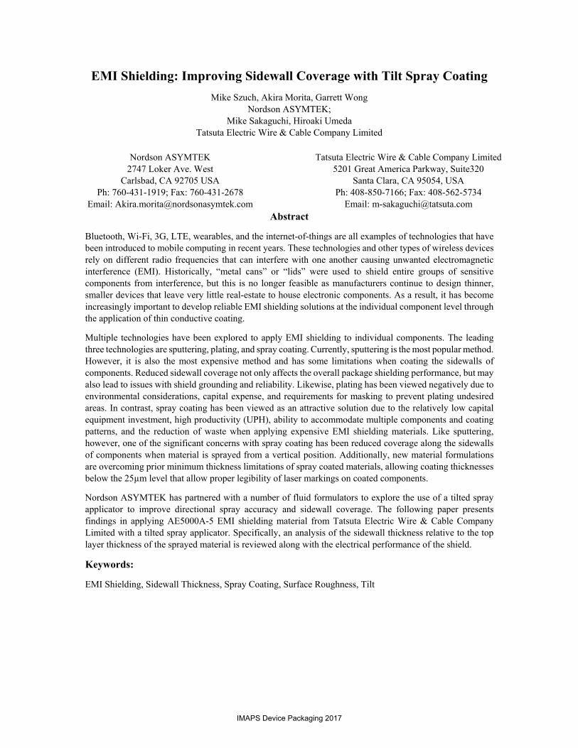
Initial attempts with spray coating of EMI shielding materials also focused on vertical spraying of the fluid. With a vertical spray, the fluid is atomized at the spray nozzle and is applied to the target component in a conical pattern with the bulk of the particles and adhesive travelling in a more vertical direction toward the target.
IMAPS Device Packaging 2017
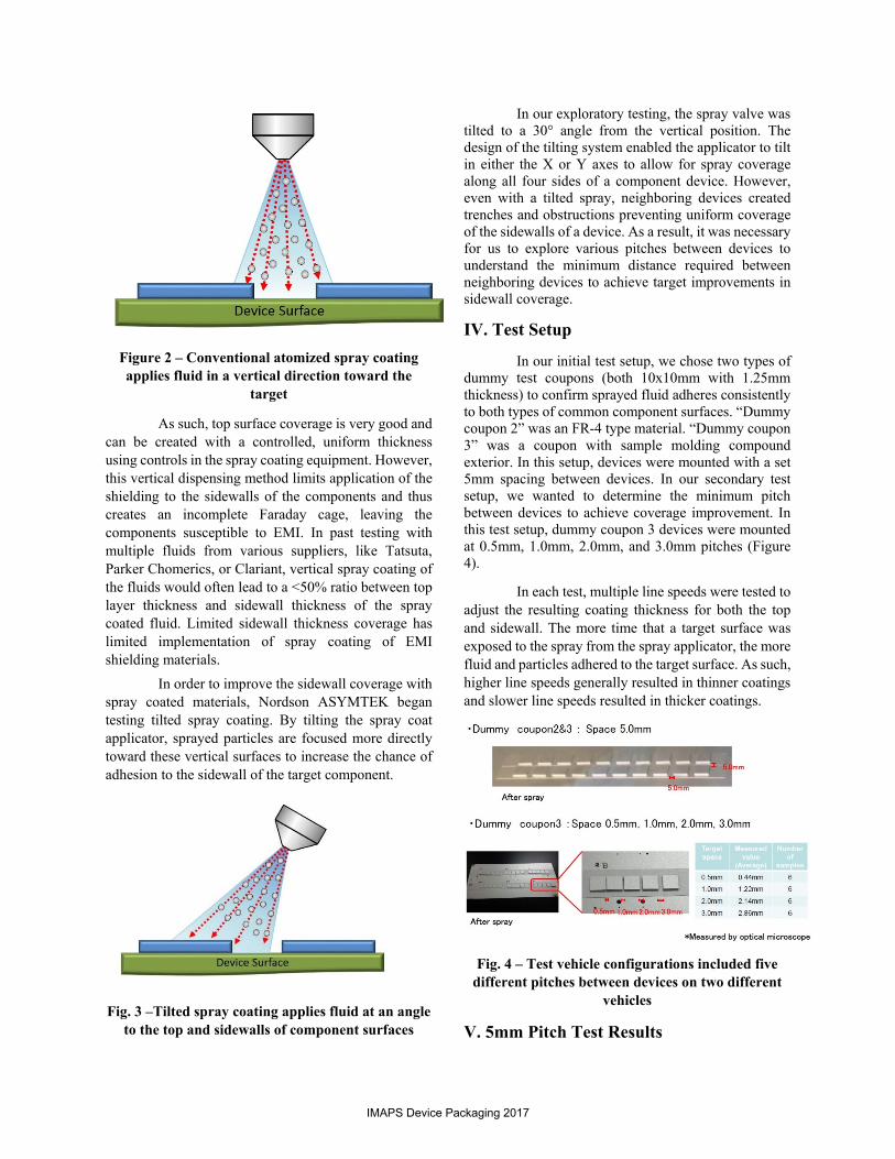
Figure 2 – Conventional atomized spray coating applies fluid in a vertical direction toward the
target
As such, top surface coverage is very good and can be created with a controlled, uniform thickness using controls in the spray coating equipment. However, this vertical dispensing method limits application of the shielding to the sidewalls of the components and thus creates an incomplete Faraday cage, leaving the components susceptible to EMI. In past testing with multiple fluids from various suppliers, like Tatsuta, Parker Chomerics, or Clariant, vertical spray coating of the fluids would often lead to a <50% ratio between top layer thickness and sidewall thickness of the spray coated fluid. Limited sidewall thickness coverage has limited implementation of spray coating of EMI shielding materials.
In order to improve the sidewall coverage with spray coated materials, Nordson ASYMTEK began testing tilted spray coating. By tilting the spray coat applicator, sprayed particles are focused more directly toward these vertical surfaces to increase the chance of adhesion to the sidewall of the target component.
Fig. 3 –Tilted spray coating applies fluid at an angle to the top and sidewalls of component surfaces
In our exploratory testing, the spray valve was tilted to a 30° angle from the vertical position. The design of the tilting system enabled the applicator to tilt in either the X or Y axes to allow for spray coverage along all four sides of a component device. However, even with a tilted spray, neighboring devices created trenches and obstructions preventing uniform coverage of the sidewalls of a device. As a result, it was necessary for us to explore various pitches between devices to understand the minimum distance required between neighboring devices to achieve target improvements in sidewall coverage.
IV. Test Setup
In our initial test setup, we chose two types of dummy test coupons (both 10x10mm with 1.25mm thickness) to confirm sprayed fluid adheres consistently to both types of common component surfaces. “Dummy coupon 2” was an FR-4 type material. “Dummy coupon 3” was a coupon with sample molding compound exterior. In this setup, devices were mounted with a set 5mm spacing between devices. In our secondary test setup, we wanted to determine the minimum pitch between devices to achieve coverage improvement. In this test setup, dummy coupon 3 devices were mounted at 0.5mm, 1.0mm, 2.0mm, and 3.0mm pitches (Figure 4).
In each test, multiple line speeds were tested to adjust the resulting coating thickness for both the top and sidewall. The more time that a target surface was exposed to the spray from the spray applicator, the more fluid and particles adhered to the target surface. As such, higher line speeds generally resulted in thinner coatings and slower line speeds resulted in thicker coatings.
Fig. 4 – Test vehicle configurations included five different pitches between devices on two different
vehicles
V. 5mm Pitch Test Results
IMAPS Device Packaging 2017

The results from the 5mm pitch test for both dummy coupons 2 & 3 resulted in similar thickness results between the component types. Depending upon line speed used (Test 1 speed was fastest with Test 3 speed slowest), top layer coating thickness was ~13µm. Sidewall thicknesses varied from 7 to 9µm depending upon line speed. The ratios between sidewall to top layer thicknesses ranged from 53% to 71%. For both components, higher line speeds resulted in better coating thickness ratios and thinner top layer thickness. Detailed results are shown in Tables I and II.
Table I – Test Results with Dummy Coupon 2 (5mm Pitch)
Table II – Test Results with Dummy Coupon 3 (5mm Pitch)
Figure 5 shows example images from cross-sectioned samples for both dummy coupons. It can be seen that coverage across both sidewalls and top surface are consistent with no pinhole breakages in the coverage. It is important to note from these images that the sprayed shield material also sufficiently covered the corners of the dummy coupons to ensure a consistent shield around the entire device.
Figure 5 – Cross-section images of 5mm pitch coating samples show no pinhole breaks
VI. Variable Pitch Test Results
In examining the sprayed shield coverage on the components, a quick gauge for shield performance can be observed from the surface roughness of sprayed material. Rougher surfaces are more prone to pinhole failures and appear more matte visually. A glossy surface finish generally denotes a more even coating with lower roughness and better consistency. As seen in Figure 7, top layer coverage and appearance was very good. However, sidewall coverage for device pitches below 2mm was poor, such that it was possible to still see underlying features from the test vehicle (copper foil lines) and indicated incomplete shield coverage.
Figure 6 – Sprayed coating delivered good top-layer coating but for device pitches below 2mm, sidewall
coverage was poor
For the testing with the variable pitch mounted dummy coupons, two line speeds were run based upon the results from the 5mm device pitch test results in Test 2 & Test 3. Sidewall thicknesses were then measured for both sides of each device to examine the effect of the
IMAPS Device Packaging 2017

device pitch on the resulting sidewall to top layer thickness ratio. In both cases, the best results were achieved at 3mm pitch between devices and resulted in comparable sidewall thickness ratios as the results from the 5mm pitch test. However results at a 2mm pitch were also notable with >50% sidewall thickness ratio. Below 2mm pitch, the sidewall coverage dropped off significantly, indicating poor coverage and matching with observed results in Figure 6.
In Tables III and IV record the results for the coating thicknesses and coating roughness measurements. Thicknesses were measured through cross-sectioning. Roughness measurements were made using confocal microscopy. Low values in coating roughness confirm spray coating uniformity and absence of pinholes.
Table III – Fast Line Speed, Variable Coupon Pitch Results
Table IV – Slow Line Speed, Variable Coupon Pitch Results
VII. Conclusion
In conclusion, test results with the Tatsuta AE5000A-5 material produced less than 15µm coating thickness with EMI shielding performance, meeting targets at the 1GHz frequency. Furthermore, sidewall to top layer thickness ratio greater than 50% was achieved when using the tilt spray applicator. It is recommended that a minimum of 2mm pitch between devices is used to achieve adequate sidewall coverage, but pitches ≥3mm will provide best coverage. Further improvements to the coverage ratio may be achieved through further fine-tuning of the dispense pattern, line speed, and spray coating parameters. Results with the Tatsuta AE5000A-5 material and Nordson ASYMTEK tilt spray application further provide performance and coverage results to rival existing EMI shielding by sputter coating processes and should be considered as a viable, lower-cost alternative for applying EMI shielding to component devices.
IMAPS Device Packaging 2017
Related Documents