Embedded Security Analysis of RFID Devices Timo Kasper July 10, 2006 Diploma Thesis Ruhr-University Bochum Chair for Communication Security Prof. Dr.-Ing. Christof Paar Co-Advised by: Dipl.-Ing. Dario Carluccio Dipl.-Phys. Kerstin Lemke-Rust

Welcome message from author
This document is posted to help you gain knowledge. Please leave a comment to let me know what you think about it! Share it to your friends and learn new things together.
Transcript

Embedded Security Analysisof RFID Devices
Timo Kasper
July 10, 2006
Diploma Thesis
Ruhr-University Bochum
Chair for Communication Security
Prof. Dr.-Ing. Christof Paar
Co-Advised by:
Dipl.-Ing. Dario Carluccio
Dipl.-Phys. Kerstin Lemke-Rust

Statement
I hereby declare, that the work presented in this thesis is my own work and that tothe best of my knowledge it is original, except where indicated by references to otherauthors.
Hiermit versichere ich, dass ich meine Diplomarbeit selber verfasst und keine anderen alsdie angegebenen Quellen und Hilfsmittel benutzt, sowie Zitate kenntlich gemacht habe.
Date / Datum Timo Kasper
ii
Contents
Statement ii
Nomenclature viii
1 Introduction 11.1 Evolution of RFID . . . . . . . . . . . . . . . . . . . . . . . . . . . . . . 1
1.1.1 History . . . . . . . . . . . . . . . . . . . . . . . . . . . . . . . . . 11.1.2 Standards for Contactless Smartcards . . . . . . . . . . . . . . . . 11.1.3 Relevant Applications . . . . . . . . . . . . . . . . . . . . . . . . 2
1.2 Motivation . . . . . . . . . . . . . . . . . . . . . . . . . . . . . . . . . . . 31.2.1 New Risks . . . . . . . . . . . . . . . . . . . . . . . . . . . . . . . 31.2.2 RF Impacts . . . . . . . . . . . . . . . . . . . . . . . . . . . . . . 31.2.3 Limitations . . . . . . . . . . . . . . . . . . . . . . . . . . . . . . 41.2.4 Privacy Considerations . . . . . . . . . . . . . . . . . . . . . . . . 41.2.5 Towards More Security . . . . . . . . . . . . . . . . . . . . . . . . 5
1.3 Related Work . . . . . . . . . . . . . . . . . . . . . . . . . . . . . . . . . 51.3.1 DEMA . . . . . . . . . . . . . . . . . . . . . . . . . . . . . . . . . 51.3.2 Relay Attack . . . . . . . . . . . . . . . . . . . . . . . . . . . . . 61.3.3 Remote Power Analysis . . . . . . . . . . . . . . . . . . . . . . . . 7
1.4 Possible Applications . . . . . . . . . . . . . . . . . . . . . . . . . . . . . 7
2 Technical Review of the ISO 14443A 82.1 RFID Operation Principle . . . . . . . . . . . . . . . . . . . . . . . . . . 8
2.1.1 Inductive Coupling . . . . . . . . . . . . . . . . . . . . . . . . . . 92.2 Communication Details . . . . . . . . . . . . . . . . . . . . . . . . . . . . 9
2.2.1 Reader → Transponder . . . . . . . . . . . . . . . . . . . . . . . . 92.2.2 Transponder → Reader . . . . . . . . . . . . . . . . . . . . . . . . 102.2.3 Initialisation Phase . . . . . . . . . . . . . . . . . . . . . . . . . . 122.2.4 Timing Specifications . . . . . . . . . . . . . . . . . . . . . . . . . 14
3 System Design and Development 163.1 The Fake Tag . . . . . . . . . . . . . . . . . . . . . . . . . . . . . . . . . 17
3.1.1 Parallel Resonant Circuit . . . . . . . . . . . . . . . . . . . . . . . 173.1.2 Protection Circuit . . . . . . . . . . . . . . . . . . . . . . . . . . . 20
iii

Contents
3.1.3 Generation of a Subcarrier . . . . . . . . . . . . . . . . . . . . . . 213.1.4 Modulation with the Subcarrier . . . . . . . . . . . . . . . . . . . 223.1.5 Load Modulation . . . . . . . . . . . . . . . . . . . . . . . . . . . 223.1.6 Acquire Miller Pulses from the HF field . . . . . . . . . . . . . . . 233.1.7 Pulsed Miller → Miller . . . . . . . . . . . . . . . . . . . . . . . . 253.1.8 Fake Tag Design Flow . . . . . . . . . . . . . . . . . . . . . . . . 26
3.2 The Reader . . . . . . . . . . . . . . . . . . . . . . . . . . . . . . . . . . 313.2.1 The RF Transceiver . . . . . . . . . . . . . . . . . . . . . . . . . . 313.2.2 Impedance Matching . . . . . . . . . . . . . . . . . . . . . . . . . 323.2.3 The RF Output Stage . . . . . . . . . . . . . . . . . . . . . . . . 323.2.4 Pulse Creation . . . . . . . . . . . . . . . . . . . . . . . . . . . . 353.2.5 Miller → Pulsed Miller . . . . . . . . . . . . . . . . . . . . . . . . 363.2.6 Modulated Manchester → Manchester . . . . . . . . . . . . . . . 373.2.7 Extra Time Delay . . . . . . . . . . . . . . . . . . . . . . . . . . . 413.2.8 Communication Link Interface . . . . . . . . . . . . . . . . . . . . 433.2.9 The Microcontroller . . . . . . . . . . . . . . . . . . . . . . . . . . 433.2.10 The Programming Adapter . . . . . . . . . . . . . . . . . . . . . 443.2.11 USB Port . . . . . . . . . . . . . . . . . . . . . . . . . . . . . . . 453.2.12 Design of the Reader – Approach and Hints . . . . . . . . . . . . 46
3.3 Tuning the Antennas for Optimum Performance . . . . . . . . . . . . . . 483.4 Software . . . . . . . . . . . . . . . . . . . . . . . . . . . . . . . . . . . . 51
3.4.1 Development Tools . . . . . . . . . . . . . . . . . . . . . . . . . . 513.4.2 Description of the Source Code . . . . . . . . . . . . . . . . . . . 52
4 Applications and Results 574.1 Low Level Reader . . . . . . . . . . . . . . . . . . . . . . . . . . . . . . . 574.2 Relay Attack . . . . . . . . . . . . . . . . . . . . . . . . . . . . . . . . . 58
4.2.1 World Cup Ticket Remarks . . . . . . . . . . . . . . . . . . . . . 594.2.2 Timing . . . . . . . . . . . . . . . . . . . . . . . . . . . . . . . . . 614.2.3 Implications on Privacy and Security . . . . . . . . . . . . . . . . 61
4.3 Timing Analysis of a Commercial RFID reader . . . . . . . . . . . . . . . 624.3.1 Tag Emulation Measurements . . . . . . . . . . . . . . . . . . . . 624.3.2 Results . . . . . . . . . . . . . . . . . . . . . . . . . . . . . . . . . 62
4.4 Antenna Tests . . . . . . . . . . . . . . . . . . . . . . . . . . . . . . . . . 634.4.1 Enhance Privacy Protection . . . . . . . . . . . . . . . . . . . . . 64
5 Future Prospects 665.1 Improved Man in the Middle Attack . . . . . . . . . . . . . . . . . . . . 66
5.1.1 Data Logging . . . . . . . . . . . . . . . . . . . . . . . . . . . . . 665.1.2 Active MITM . . . . . . . . . . . . . . . . . . . . . . . . . . . . . 67
5.2 Increasing the Range . . . . . . . . . . . . . . . . . . . . . . . . . . . . . 675.3 Improvement of DEMA . . . . . . . . . . . . . . . . . . . . . . . . . . . . 68
iv

Contents
5.4 Power Analysis . . . . . . . . . . . . . . . . . . . . . . . . . . . . . . . . 685.5 Fault Attacks . . . . . . . . . . . . . . . . . . . . . . . . . . . . . . . . . 685.6 Implementation of any Protocol . . . . . . . . . . . . . . . . . . . . . . . 68
6 Conclusion 70
A Bibliography 71
B Layout and Schematics 75
C Source Code Version 0.95 82C.1 board.h . . . . . . . . . . . . . . . . . . . . . . . . . . . . . . . . . . . . 82C.2 em4094lib.c . . . . . . . . . . . . . . . . . . . . . . . . . . . . . . . . . . 83C.3 etcetera.c . . . . . . . . . . . . . . . . . . . . . . . . . . . . . . . . . . . 97C.4 ftlib.c . . . . . . . . . . . . . . . . . . . . . . . . . . . . . . . . . . . . . 102C.5 test.c . . . . . . . . . . . . . . . . . . . . . . . . . . . . . . . . . . . . . . 106C.6 Makefile . . . . . . . . . . . . . . . . . . . . . . . . . . . . . . . . . . . . 109
v
List of Figures
1.1 Separating the chip and the plastic packaging of a smartcard . . . . . . . 6
2.1 General RFID System . . . . . . . . . . . . . . . . . . . . . . . . . . . . 82.2 (Pulsed) Miller Coding . . . . . . . . . . . . . . . . . . . . . . . . . . . . 102.3 Modulation Principle . . . . . . . . . . . . . . . . . . . . . . . . . . . . . 112.4 (Modulated) Manchester Coding . . . . . . . . . . . . . . . . . . . . . . . 122.5 States of a tag during the initialisation phase . . . . . . . . . . . . . . . . 13
3.1 System Overview . . . . . . . . . . . . . . . . . . . . . . . . . . . . . . . 163.2 Operation Principle of the Fake-Tag . . . . . . . . . . . . . . . . . . . . . 173.3 Parallel resonant circuit . . . . . . . . . . . . . . . . . . . . . . . . . . . 183.4 Impedance of a parallel resonant circuit, with Q varied . . . . . . . . . . 193.5 Influence of the Q factor on the received signal . . . . . . . . . . . . . . . 203.6 Typical characteristic curve of a Zener diode . . . . . . . . . . . . . . . . 213.7 Frequency Division by 16 to obtain the Subcarrier . . . . . . . . . . . . . 213.8 Realisation of the switch for the load modulation . . . . . . . . . . . . . 223.9 The adaptive envelope detector of the Fake Tag . . . . . . . . . . . . . . 233.10 Fall times of the RC-circuits . . . . . . . . . . . . . . . . . . . . . . . . . 243.11 Delay induced by the envelope detector . . . . . . . . . . . . . . . . . . . 253.12 Conversion of Miller Pulses to normal Miller coded data . . . . . . . . . 253.13 Transformation of the signal between antenna and communication interface 263.14 The Coffee Cup Tag . . . . . . . . . . . . . . . . . . . . . . . . . . . . . 273.15 Experimental extensions of the Coffee Cup Tag . . . . . . . . . . . . . . 283.16 The Fake Tag, version 1 . . . . . . . . . . . . . . . . . . . . . . . . . . . 293.17 The PCB of version 2 of the Fake Tag . . . . . . . . . . . . . . . . . . . 293.18 Layout and dimensions of the Fake Tag, version 2 . . . . . . . . . . . . . 303.19 The Reader . . . . . . . . . . . . . . . . . . . . . . . . . . . . . . . . . . 313.20 Schematic of the Output Stage . . . . . . . . . . . . . . . . . . . . . . . 333.21 Impedance Matching with a Smith Chart . . . . . . . . . . . . . . . . . . 343.22 Wiring of the monoflop for generation of pulses . . . . . . . . . . . . . . 363.23 Recreation of pulses from the Miller coded input data . . . . . . . . . . . 363.24 Ideal and real signal at the DOUT pin of the EM4094 transceiver . . . . 373.25 The envelope detector of the reader with surrounding circuitry . . . . . . 383.26 Step by step: Demodulation of the transceiver’s DOUT signal . . . . . . 39
vi

List of Figures
3.27 Antenna field, DOUT of EM4094 and relayed signal at the fake tag . . . 403.28 Delay induced by the Internal Signal Processing of the EM4094 Transceiver 403.29 Schematic of the Extra Delay . . . . . . . . . . . . . . . . . . . . . . . . 413.30 Simulation and Measured Performance of the Extra Delay . . . . . . . . 423.31 Manchester Coded Output of the Demodulation Stage . . . . . . . . . . 423.32 The readily assembled program adapter . . . . . . . . . . . . . . . . . . . 443.33 Schematic of the program adapter . . . . . . . . . . . . . . . . . . . . . . 453.34 The completely assembled first version of the reader . . . . . . . . . . . . 473.35 Experimental extensions of the first reader version . . . . . . . . . . . . . 483.36 The PCB of the second version of the reader . . . . . . . . . . . . . . . . 493.37 Setup for the tuning of the antennas . . . . . . . . . . . . . . . . . . . . 50
4.1 Testing the Low Level Reader with a German e-passport . . . . . . . . . 574.2 Principle of a Relay Attack . . . . . . . . . . . . . . . . . . . . . . . . . . 584.3 Relaying a ticket for the world championship . . . . . . . . . . . . . . . . 604.4 Sunlight from behind reveals the secrets of the world championship ticket 614.5 Induced delay during a relay attack . . . . . . . . . . . . . . . . . . . . . 624.6 Measured behaviour of the ACG reader . . . . . . . . . . . . . . . . . . . 634.7 Wire and PCB antennas with different dimensions . . . . . . . . . . . . . 644.8 Setup for range measurements . . . . . . . . . . . . . . . . . . . . . . . . 65
B.1 Layout of the Fake Tag, Version 1 and Version 2 . . . . . . . . . . . . . . 75B.2 Schematic of the Fake Tag, Version 2 . . . . . . . . . . . . . . . . . . . . 76B.3 Top and Bottom Layer of the Program Adapter . . . . . . . . . . . . . . 77B.4 Schematic of the Program Adapter . . . . . . . . . . . . . . . . . . . . . 78B.5 Layout of the Reader, Version 2 . . . . . . . . . . . . . . . . . . . . . . . 79B.6 Top and Bottom Layer of the Reader, Version 2 . . . . . . . . . . . . . . 80B.7 Schematic of the Reader, Version 2 . . . . . . . . . . . . . . . . . . . . . 81
vii

Nomenclature
CLn Cascade Level n
AC Alternating Current
ADC Analog to Digital Converter
AES Advanced Encryption Standard
ASK Amplitude Shift Keying
ATQA Answer To Request, Type A
ATS Answer To Select
CMOS Complementary Metal-Oxide Semiconductor
DC Direct Current
DDR Data Direction Register
DEMA Differential ElectroMagnetic Analysis
DES Data Encryption Standard
DIP Dual In-line Package
DPA Differential Power Analysis
ECC Elliptic Curve Cryptography
EOC End Of Communication
FDT Frame Delay Time
FIFO First In First Out
HF High Frequency
HLTA Halt command, Type A
IC Integrated Circuit
IDE Integrated Development Environment
ISR Interrupt Service Routine
LED Light Emitting Diode
LF Low Frequency
MISO Master In Slave Out
MOSFET Metal-Oxide Semiconductor Field-Effect Transistor
viii

Nomenclature
MOSI Master Out Slave In
MRTD Machine Readable Travel Document
MSB Most Significant Bit
NDA Non Disclosure Agreement
NFC Near Field Communication
NOP No Operation (computer processor instruction)
NRZ Non Return to Zero
NVB Number of Valid Bits
OOK On Off Keying
PC Personal Computer
PCB Printed Circuit Board
RAM Random Access Memory
RATS Request Answer To Select
REQA Request command, Type A
RF Radio Frequency
RFID Radio Frequency IDentification
RISC Reduced Instruction Set Computer
ROM Read Only Memory
SAK Select AcKnowledge
SCK Slave Clock
SEL SELect code command
SMD Surface Mounted Device
SNR Signal to Noise Ratio
SOC Start Of Communication
TTL Transistor-Transistor-Logic
UART Universal Asynchronous Receiver-Transmitter
UHF Ultra High Frequency
UID Unique IDentifier
USB Universal Serial Bus
VCP Virtual Com Port
WUPA Wake-Up command, Type A
ix

1 Introduction
1.1 Evolution of RFID
1.1.1 History
When the notion of Radio-Frequency Identification (RFID) arose in the 1940s, it wasused for identification of objects, i.e., allied airplanes by the military forces [46]. The so-called active tags needed a power supply, had rather large dimensions and carried smallamounts of data, e.g., a fixed unique number. As technology evolved, with modernsilicon wafer manufacturing, chip sizes with an area as small as 0.15×0.15 mm2 and athickness of only 7.5 μm are possible [19], resulting in lower energy consumption. Thisenables passive tags, which draw the energy needed for operation completely from theRF1 field that is generated by a reader device. At the same time, it is now possible to putmuch larger memories and even microcontrollers with crypto co-processors on the chipof the tag, so that applications like contactless, cryptographically enabled smartcardsand their use as credit cards or digital passports are becoming widespread and RFIDcan be an ubiquitous technology.
1.1.2 Standards for Contactless Smartcards
Different standards are available for RFID technology, described in more detail in theRFID handbook [15], operating at frequencies from 135 kHz in the LF2 range to 5.8 GHzin the UHF3 range. The relevant ones for cryptographic applications, almost exclusivelyoperated in the HF4 range at 13.56 MHz, are mentioned briefly. Table 1.1 shows acomparison of the standards with regard to operating frequency, approximate operatingrange and maximum data rate.
The standard for closely coupled smartcards, namely the ISO 10536, was developedbetween 1992 and 1995 and never succeeded in the market, due to high manufacturingcosts and only small advantages compared to contact-based cards.
The ISO 14443 standard for proximity coupling, described in Section 2, is often thechoice for access control and ticketing purposes.
1Radio Frequency2Low Frequency3Ultra High Frequency4High Frequency
1

1 Introduction
Vicinity cards, as specified in the ISO 15693, can be read from a greater distance,compared to proximity cards, at the cost of a lower data rate. In addition, the energyconsumption of an ISO 15693 compliant tag has to be lesser, due to a lower specifiedmagnetic field strength being necessary for operation which, combined with the lowdata rate, very likely makes state-of-the-art cryptography impossible. Note that themaximum operating range, given in Table 1.1, is only achievable using the long distancemode of ISO 15693 compliant tags, for which a data rate of only 1.65 kBit/s is specified.
The NFC5 standard has been pushed mainly by Philips and Sony, is compatible tothe ISO 14443 A standard, and shall be used for short-range communication betweenelectronic devices [43].
Standard Card Type Range Frequency Data Rate
ISO 10536 Close Coupling ≤ 1 cm 4.9152 MHz 9600 Bit/sISO 14443 Proximity Coupling 8 ... 15 cm 13.56 MHz 847.5 kBit/sISO 15693 Vicinity Coupling 1 ... 1.5 m 13.56 MHz 26.48 kBit/sISO 18092 Near Field Communication ≈ 10 cm 13.56 MHz 424 kBit/s
Table 1.1: Comparison of standards for contactless smartcards
1.1.3 Relevant Applications
The ISO 14443 standard [22] is employed by many leading chip manufacturers in var-ious RFID applications, e.g., Mifare identification chips from Philips6, which are usedfor ticketing, during the world championship 2006 in Germany [45] and for public trans-port in the London Underground [4], or Texas Instruments’ chips being implanted inMasterCard’s PayPass [3] and Visa Contactless RFID payment cards [2]. At the RuhrUniversity in Bochum, contact based smartcards have recently been upgraded with acontactless prepaid payment function, which is based on the ISO 14443 standard andenables, for example, the automatic recognition, if a discount is to be granted, dueto the status (student, employee, pensioner, etc.) of the respective person. Anothercrucial application is the digital passport (e-passport), standarised by the InternationalCivil Aviation Organization (ICAO)7, in which an ISO 14443 compliant chip [5] storesbiometric data [8], in addition to the personal particulars.
New inventions like wearable RFID wristbands or transponders implanted in shoes,and even tags injected under the skin of human beings, are nowadays used instead of a keyto gain access to restricted areas. Identification and tracking purposes (e.g., of children,elderly people, patients in a hospital) might become pervasive in the near future. Tagged
5Near Field Communication6http://www.semiconductors.philips.com7http://www.icao.int
2

1 Introduction
money is one more vision, with RFID chips in the paper, to make counterfeiting moredifficult, or tagged airline baggage, to ease automatic transportation.
In general, a wide deployment of the ISO 14443 standard can currently be noticedfor contactless applications demanding for privacy and security, with the resulting needfor high computation power, which at the moment can only be achieved via inductivecoupling (see Section 2.1.1) and a relatively short reading distance.
1.2 Motivation
1.2.1 New Risks
As with every new technology, new threats appeared with the deployment of RFID,beginning in the 1950s, when enemies airplanes pretended to be from the other partyby replaying a previously recorded answer. This demanded for inventions like Feistel’stwo pass authentification challenge, which, in extended variations, is still often usedto prevent such attacks in modern RFID systems [46]. Moreover, the interchangeddata is often encrypted with common block ciphers [35] like AES8 and (Triple-)DES9,or sometimes even public-key algorithms like ECC10, where security or privacy issuesare relevant. Still, modern offenders get physical access to the chip or its field andperform so called side channel attacks [36] like a DPA11 or a DEMA (see Section 1.3.1),which make it possible to obtain a secret key stored on the device by analysing thepower consumption or electromagnetic emanation over the time and correlating it witha data hypothesis and the code being executed. Other implementations of attacks aimat introducing an error during computation of a device, which can ease cryptanalysis.
1.2.2 RF Impacts
The physical interface of contactless smartcards brings new opportunities for possibleattackers, because the wireless transmission of data via the RF12 field can easily beeavesdropped by an attacker, without the carrier of the tag taking note of it. So sniffing,i.e. acquiring and analysing the data transmitted between reader and tag to obtain a cer-tain information, for example someone’s photo or fingerprint, is possible over sometimeslarge ranges. Eavesdropping of communication between ISO 14443 compliant devicesover a distance of several meters has been performed by Finke and Kelter [14]. The com-munication data can be recorded, collected and maybe decrypted later on. People alsocan be tracked, for example by a set of tagged items, which were recently bought and
8Advanced Encryption Standard9Data Encryption Standard
10Elliptic Curve Cryptography11Differential Power Analysis12Radio Frequency
3

1 Introduction
carried around by an individual, whose movings then can be monitored. A relay (pas-sive man-in-the-middle) attack is also feasible, i.e., redirecting the data interchangedbetween reader and tag over a separate communication channel to pretend to be theowner of someone else’s tag. The data could be manipulated in a way that gives someadvantage to the attacker before relaying the data - an active man-in-the-middle attack.The number of possible threats is large and becoming larger, showing the necessity ofwell designed security schemes in the various systems.
1.2.3 Limitations
The energy consumption, i.e., the maximum number of switching transistors of a passiveRFID tag is limited [27], whilst having the advantages of smaller size, lower weight andless cost. Typical implementations using a 0.35 μm process have 5000 gates and consumea current of 15 μA [46]. Furthermore, as the industry wants to keep the prices low,security measures and physical protection on the chip, demanding for much chip area,may be rarely implemented. Hence, certain mechanisms to protect devices against sidechannel- and other attacks will be very lightweight or won’t be found at all on someRFID devices [34].
Some proprietary RFID systems have already been broken, for example the DigitalSignature Transponder (DST), manufactured by Texas Instruments, employed in vehicleimmobilisers that are used additionally to carry out payments. Bono et al.[7] reverseengineered the protocol, decrypted the communication, i.e. figured out the secret key,and, in addition, purchased gasoline and started an automobile by simulating DSTdevices.
1.2.4 Privacy Considerations
Civil Liberties groups and other organisations, e.g., the FoeBud in Germany with their“stop RFID” campaign13, fear the abuse of RFID based applications and warn peoplenot to ignore threats like universal surveillance and violations of the privacy of individ-uals. Medical information getting into the wrong hands might result in unemployment,and tracking of movements, for example by tagging employees at the workplace, in asignificant loss of privacy.
It is important on the one hand not to exaggerate these problems and thus provokefears in the population, and on the other hand not to underestimate these challengesand find solutions, to profit from the advantages of the modern technology and at thesame time protect it from being misused.
13http://www.foebud.org/rfid
4

1 Introduction
1.2.5 Towards More Security
In order to improve the security analysis of RFID systems, tools providing the contactlessinterface and being able to perform known attacks, as well as to analyse the capabilitiesand functionality of the hardware used in an RFID system, need to be developed. As thestandards for contactless smartcards differ very much with regard to operating frequency,communication interface and transmission protocol [15], the hardware for a reasonablesecurity analysis must be quite specialised and tailored to one certain standard.
The RFID tool, that is developed and built up as a part of this diploma thesis, isgenerally applicable to all devices compliant to part 2 (RF power and signal interface)and part 3 (initialisation and anticollision) of the ISO 14443(A) [22], no matter if aproprietary protocol, including cryptography, is implemented on a higher layer.
1.3 Related Work
1.3.1 DEMA
A DEMA14 is a special form of electromagnetic side channel analysis of cryptographic ICsand, as shown by Carluccio et al.[10], can be applied to RFID smartcards. An antennaconnected to an oscilloscope, placed as close as possible to the chip for obtaining ahigh Signal to Noise Ratio (SNR), is used to gather information about the secret keystored on the device, by measuring and evaluating the electromagnetic emanation duringoperation. To reduce the influence of the RF interface on the measurements and tofurther increase the SNR, the chip can be removed from the plastic packaging and theantenna separated from it, as depicted in Figure 1.1. Now, the communication betweenan RFID reader and the smartcard, via the antenna, which remains in the plastic of thecard in the background of the picture, can take place spatially and electrically separatedfrom the measurements with the chip, in the foreground of the picture.
As DEMA is based on a statistical test, for which subsequent measurements haveto be synchronised and superimposed without too much jitter, it is helpful to have areliable signal to trigger the scope.
The protocol of the Philips Mifare DESFire contactless smartcard, i.e., the appliedmutual three pass authentification, has been reverse engineered [9] until to the pointnecessary for carrying out a DEMA to potentially achieve the secret key stored on thedevice. In the attack performed by Carluccio, so-called challenges, needed for the men-tioned authentification protocol, were generated by a commercial RFID reader deviceand had to be extracted from the communication data afterwards, which was very timeconsuming. As the protocol used was readily implemented in the reader, the commu-nication could not be aborted (and then restarted) at any moment, i.e., after willinglysending invalid data.
14Differential Electro Magnetic Analysis
5

1 Introduction
Figure 1.1: Separating the chip and the plastic packaging of a smartcard
1.3.2 Relay Attack
A relay attack, also called a passive man-in-the-middle attack, without being able tomodify the data interchanged between reader and tag, as described by Kfir and Wool [23],was practically carried out by Hancke [17]. The special feature of this attack is, that itworks on the physical layer and therefore can not be prevented by basic authentificationprotocols and encryption of the data interchanged. The antenna of a reader, possessedby the offender, has to be placed close enough to the contactless card or tag of a victim,while a second device emulating a tag is brought into the field of an RFID reader, e.g.,at a cash desk possibly located at a distance from the owner of the card. The data beingtransferred by this reader is acquired and directly forwarded on the bit layer through acommunication link to the reader of the attacker. There, the data is retransmitted tothe card of the victim, which then answers to the request of the remote reader, withoutits owner noticing it. The answer is relayed back via the device emulating a tag to thecashpoint’s reader again and so, as the attacker continues relaying the data, both readerand tag will be convinced, that they are in close vicinity to each other, share the samesecret and carry out their task, e.g., authorise a payment.
Hancke and Kuhn [18] proposed a possible countermeasure against these kind of at-tacks, based on ultra-wideband pulse communication. This method is not being em-ployed in devices currently available on the market, so still the most effective way to cir-cumvent such an attack, for the devices currently in use, is to construct a Faraday’s cagearound the tag, e.g., by wrapping it with aluminum foil (investigated in Section 4.4.1).
6

1 Introduction
1.3.3 Remote Power Analysis
Another power analysis attack requiring no physical contact to the device was performedby Oren and Shamir [34], with RFID tags operating in the UHF range, where so calledbackscattering is used for data transmission from tag to reader, instead of inductivecoupling (see Section 2.1.1) in the HF range, as specified in the ISO 14443. Similar tothe ISO 14443, the data is transferred from a reader to a tag by the use of gaps in thefield of the reader (compare with Section 2.2.1), which at the same time has to providethe energy needed for operation of the tag. During the pauses, the tag draws the energyfrom a built in capacitor, which needs to be recharged when the field is turned on again.This leads to different shaped energy peaks occurring after the gaps, depending on theamount of power consumed by the tag during the pause, noticeable at the antenna ofthe reader. This behaviour was exploited to find an 8-bit password for the kill commandof EPC Global tags. The described method may also be applicable to transponderscompliant to the ISO 14443, which has to be further researched.
1.4 Possible Applications
The devices developed here shall ease the security analysis of cryptographically enabledRFID devices with an ISO 14443A compliant RF interface, and make it possible toperform the following tasks:
• use of a transparent and flexible contactless interface on the bit layer, i.e., animplementation of a low level reader,
• emulation of an RFID tag,
• replay attack,
• relay attack,
• active MITM (man-in-the-middle) attack, i.e. possibility to intervene in the com-munication,
• investigations of conformance to the ISO 1444315,
• (remote) power analysis,
• DEMA,
• fault analysis,
• analysis of protocols, i.e., logging of the communication data,
• fast communication with a PC or other cryptographic hardware via USB,
• testing of different types of antennas and tuning methods in diverse environments.
15experiments with the tool developed in this thesis showed, that an RFID reader did not strictly obeytiming requirements specified in the ISO 14443 and so eventually facilitates relay attacks
7

2 Technical Review of the ISO 14443A
This work focuses on devices compliant to the ISO 14443 A standard, using a data rate offc
128, where fc denotes the carrier frequency of the reader, leading to 13.56 MHz
128= 106 kBit
s
in both directions, as specified in part 2 of the standard [22]. In this thesis, the termstag, card and transponder are used equivalently, and are therefore interchangeable.
2.1 RFID Operation Principle
Figure 2.1: General RFID System
A minimum RFID system consists of two main components, namely a reader gener-ating a field, i.e., a sine wave with a frequency of 13.56 MHz, which supplies the secondcomponent for the system, a so called tag or transponder, with energy1 and often aclock signal for operation of its digital circuits [15]. A chip on the tag contains data,which may be fixed and stored in a ROM, or changeable and stored in a RAM, andfurthermore must have the capability to en- and decode the information interchangedwith the reader. For more sophisticated applications, microcontrollers and operatingsystems for comfortable access to the stored data, and cryptographic co-processors, toencipher the communication, are employed. Both transponder and reader are equippedwith a coupling element, which in the case of the ISO 14443 is a coil with typically3-10 windings, permitting data transfer in both directions. Note, that the term RFIDreader is a rather misleading description for a device that does not only receive datafrom the tag, but of course also transmits data to it, while often being connected toanother system, e.g., a PC (Personal Computer).
1in the case of passive tags
8

2 Technical Review of the ISO 14443A
2.1.1 Inductive Coupling
The wavelength λ of an electromagnetic field is calculated following equation 2.1, where cdenotes the speed of light and f the carrier frequency, which here is equal to 13.56 MHz,as defined in the standard.
λ =c
f=
3 · 108 ms
13.56 MHz≈ 22.1 m (2.1)
Obviously, the derived wavelength is several times greater than the typical operatingdistance between reader and tag, which is approximately 8-15 cm [15]. Accordingly, thefield emitted from the coil of the reader may be treated as purely magnetic2, leading tothe term inductive coupling being used to describe the communication- and energy linkbetween reader and tag.
2.2 Communication Details
According to the ISO 14443, a reader transmits data to a tag by means of switchingthe field temporarily off, i.e., create short gaps in the field, which are detected anddecoded by the tag. The tag answers employing load modulation as described below inSection 2.2.2, which in turn is sensed and decoded on the side of the reader.
The communication is based on a master-slave principle, where the reader is alwaysthe master, and the tag is the slave. The reader talks first, and then listens to the answerof the tag3, while keeping the field alive to supply it with energy.
1. reader sends data to the tag (termed downlink)
2. waiting time until to the answer of the tag
3. tag answers (termed uplink)
4. waiting time until to the next request from the reader
...proceed with 1 until finished.
2.2.1 Reader → Transponder
For the downlink, modified (pulsed) Miller coding is used, where the data is representedas follows.
2similar to the common transformer principle3a so called half duplex system
9

2 Technical Review of the ISO 14443A
Modified Miller Coding
The correlation between NRZ4, Miller code and the modified variant (at the bottom) isdepicted in Figure 2.2.
Figure 2.2: (Pulsed) Miller Coding
• Logic 1 : Pause in the middle of the bit period, i.e. after 64fc
≈ 4.72 μs
• Logic 0
α) previously 0 or SOC 5: Pause at the beginning of the bit period
β) previously 1 : No modulation for the full bit duration.
• SOC : Pause at the beginning of a bit period (equals 0 after 0 )
• EOC 6: Logic 0 followed by no modulation for a full bit period
Pauses have to be created with a duration of approximately 2.5 μs7, with 100% ASK8,i.e., the field has to be completely switched off and on by the reader.
2.2.2 Transponder → Reader
Load Modulation
As explained in Section 2.1.1, the energy consumed by a tag is supplied by the readervia the two transformer-like coupled coils of the RFID system. The resulting feedback of
4Non Return to Zero5Start Of Communication6End Of Communication7more precise between 2 and 3 µs8Amplitude Shift Keying
10

2 Technical Review of the ISO 14443A
the transponder, drawing more or less energy from the field, can be sensed by a varyingamplitude at the antenna of the reader. By switching on and off an additional loadresistor and thereby deliberately taking more energy from the field than during normaloperation, the tag transmits its data to the reader, sometimes referred to as OOK9 in theliterature. As the coupling between tag and reader is weak and the resulting effect onthe field almost not noticeable, a subcarrier of the reader’s carrier frequency is generatedby the tag and used to switch the resistor, leading to the transmitted information beingplaced in sidebands of the carrier and making the detection of the achieved 10 mV changeof useful signal at a carrier amplitude of 100 V10 possible [15].
Figure 2.3: Modulation Principle
Figure 2.3 illustrates the described process: On the left side, a low pass filtered sig-nal containing the information to be transmitted, e.g. a 106 kBit/s data stream, hasbeen modulated with a 847 kHz subcarrier, as described in Section 3.1.5, resulting inthe depicted symmetric frequency spectrum11, which can be obtained by performing aFourier transform (see [13] for details). Modulating this signal again with a 13.56 MHzsine wave leads to the frequency spectrum on the right side of Figure 2.3, where the left,symmetric half of the spectrum is omitted. Obviously, the information is being placedin sidebands beside the carrier frequency.
(Modulated) Manchester Coding
For the uplink, the described load modulation is utilised to transmit Manchester encodeddata, modulated with a subcarrier of fc
16= 847.5 kHz, which shall be synchronous to the
field of the reader. Figure 2.4 illustrates the generation of the modulated code. One bitduration equals eight subcarrier-periods at the data rate of fc
128= 106 kBit/s.
• Logic 1 : Falling edge at the centre, i.e., modulation with the subcarrier for thefirst half of the bit period
9On Off Keying10corresponding to 80dB11all real world signals have a symmetric frequency spectrum
11

2 Technical Review of the ISO 14443A
• Logic 0 : Rising edge at the centre, i.e., modulation with the subcarrier for thesecond half of the bit period
• SOC : Equals logic 1 (see above)
• EOC : No modulation for a full bit period
Figure 2.4: (Modulated) Manchester Coding
Manchester coding may be alternatively viewed as a phase encoding, where each bit isencoded by a positive 90 degree phase transition or a negative 90 degree phase transition,and therefore is sometimes referred to as biphase coding.
Note that, when Manchester coding is employed, a reader can easily detect two cardssending distinct bits simultaneously, as this leads to a modulation for a full bit period.This is of use during the anticollision phase of the ISO 14443 protocol.
2.2.3 Initialisation Phase
Collisions between two tags being in the same field, answering simultaneously to a requestof a reader, and thus preventing it from acquiring valid data from any of the tags,usually don’t play a role due to the short operating range. Hence, the anticollision partof the protocol is not explained here, and, in the following brief description of a typicalcommunication sequence, it is assumed that only one card is present in the field of areader. The following section shall give only an idea of the protocol – further details canbe found in part 3 of the standard [22].
Initialisation Sequence
When getting in the proximity of a reader, into an energizing magnetic field greater thanHmin
12= 1.5 Am
(details in the standard [22], part 2), the card powers up and gets into
12a maximum unmodulated operating field, with a value of Hmax = 7.5 Am , is also defined
12

2 Technical Review of the ISO 14443A
Figure 2.5: States of a tag during the initialisation phase
the idle state.A REQA13 or WUPA14 induces emission of an ATQA15 and a change into the ready
state, where the card waits for a SEL16 of Cascade Level n (CLn) with the parameterNVB17 being 0x20, prompting the card to answer with its UID18 of CLn. The readeracquires this UID and can now issue a SELECT command with the UID of the tag.
The card answers to the SELECT command with its SAK 19 response, which indicates,whether the UID is already complete (or a higher cascade level has to be handled) andif it is part 4 - compliant. As the ISO allows for 3 different lenghts of the UID (4,7 or10 bytes), the above process (SEL etc.) might have to be repeated up to 3 times, eachtime with a higher CL, until the card has received its complete UID and finally goes
13Request command, Type A14Wake-Up command, Type A15Answer To Request, Type A16SELect code command17Number of Valid Bits18Unique IDentifier19Select AcKnowledge
13

2 Technical Review of the ISO 14443A
into the active state. From there on, commands according to a higher layer protocol(ISO14443 [22] part 4, or a proprietary protocol) can be issued.
In case of compliance to part 4, the reader sends an RATS 20 now, containing themaximum possible framesize it can handle, answered by an ATS 21 of the tag. The ATSdefines the maximum framesize accepted by the tag, as well as the bit rate capabilitiesof the tag in both directions.
After having entered at least the active state, a card can enter a halt state for exampleby receiving a HLTA22, from which it only answers to a WUPA, but not to a REQA.The rest is similar to the normal case described above. A card in any state receiving aREQA will become either idle or enter the halt state.
The concrete implementation of the necessary commands is specified in the ISO 14443.
UID Concerns
Every ISO 14443A compliant RFID tag has an own UID, which is often a fixed number,written into the ROM of the chip by the manufacturer, but can also be a randomnumber, dynamically created every time the device powers up - important, for example,to prevent tracking of individuals by scanning the UID of their e-passport. If the firstbyte of the UID equals 0x08, it is a randomly generated number, otherwise it will be aproprietary fixed number. During tests with an e-passport, the described behaviour wasverified.
2.2.4 Timing Specifications
As the timing requirements of the ISO14443A ([22], part 3 and 4) are important for theemulation of a tag or performing a relay attack, which is naturally inducing a certaindelay, they are discussed here in detail.
Request Guard Time
Between the start bits of several consecutive REQA commands, a pause of 7000fc
≈ 516 μs,called request guard time, has to be inserted.
Frame Delay Time
The frame delay time FDT is the time between two frames transmitted in oppositedirections and specified in part 3 of the standard [22].
Tag → Reader: The time between the end of the last pause created by the readeruntil to the first edge of the answer of the tag shall be
20Request Answer To Select21Answer To Select22Halt command, Type A
14

2 Technical Review of the ISO 14443A
After a logic 1 :
FDT =(128 · n + 84)
fc
(2.2)
If the reader sent a logic 0 :
FDT =(128 · n + 20)
fc
(2.3)
For specific commands like REQA or WUPA, the integer value n equals n = 9,which leads to a pause duration of 1236
fc≈ 91.15 μs if the last bit sent by the reader
was a logic 1, or 1172fc
≈ 86.43 μs if it was a logic 0. For all other commands, n ≥ 9applies. In any case, the first edge of the answer of the tag has to be aligned tothe bit grid defined above.
Furthermore ISO 14443 [22] part 4 defines an activation frame waiting time, whichis the maximum time for a card to answer after the EOC of the reader’s requestand equals 65536
fc≈ 4.8 ms.
Reader → Tag: The minimum time between the last modulation of the tag until tothe first gap in the field, generated by the reader, is
FDT =1172
fc
≈ 86.43 μs (2.4)
Note that for the time between a command of the reader and the answer of a tag, exceptfor the case n = 9, only a bit grid with an upper bound is specified, whereas, in theopposite direction, solely a minimum time has to be considered.
15

3 System Design and Development
The system developed in this thesis consists of a multi purpose reader device, whichis equipped with a microcontroller, an RF interface and the ability to do some signalprocessing. A second device, named fake tag, is able to perform load modulation andto gather the information sent by a remote reader. If properly fed with data, thisfake tag appears like an authentic tag to an RFID reader. Between the two units, acommunication link can be established, which is just a cable or can be wireless.
Figure 3.1: System Overview
The RFID tool can be integrated in a complete system, consisting of a PC, the de-veloped reader and fake tag, a digital oscilloscope and more measurement equipmentlike near field probes to quantify electromagnetic emanation. Reader and scope are con-nected to the PC, which controls the process sequence and later combines and furtherhandles the data acquired from scope and reader.
The developed hardware permits automatic recognition of the information interchangedand its transfer to a PC or specialised hardware [25] for cryptographic analysis, maybereal time decrypting of the data transmitted, or other processing.
In addition, stand alone operation of the RFID tool is possible, to execute man-in-the-middle attacks or store data acquired from RFID tags maybe without permission,
16

3 System Design and Development
e.g., in the subway or other crowded places, where the required short reading distancecan be accomplished. If the information is not encrypted, it could be modified and laterreplayed via the fake tag to make an RFID reader believe to have, for example, a validticket in its vicinity.
The RFID tool was built using electronic hobbyist equipment and materials, withcommonly available components. Therefore, since the tool has been developed now, thereproduction is feasible without much competence, at a cost of well beyond 50 e.
3.1 The Fake Tag
Figure 3.2: Operation Principle of the Fake-Tag
The Fake Tag, which is designed to appear like an authentic ISO 14443 compliantRFID transponder, is intended to cooperate with the developed RFID reader (see Sec-tion 3.2) and can be utilised for relay and replay attacks as well as for tag emulation.Unlike a normal (passive) tag, the fake tag described here has an own power supply1,which can also be used for supplying an optional wireless module.
3.1.1 Parallel Resonant Circuit
To be able to communicate with a reader, a tag needs a coil as an antenna to establishthe coupling to the counterpart of the reader. A capacitor is connected in parallel to thisinductance to form a parallel resonant circuit with a resonant frequency correspondingto the carrier frequency of, in this case, 13.56 MHz.
For an ideal parallel resonant circuit, capacitance and inductance are selected ac-cording to equation 3.1, where f0 denotes the carrier frequency of the reader, C thecapacitance and L the inductance of the tuned circuit [50].
1can be a small lithium battery
17

3 System Design and Development
Figure 3.3: Parallel resonant circuit
f0 =1
2π · √LC(3.1)
In practice, first the value for L is derived from the shape and dimensions of the coil2,afterwards the optimal C is calculated according to equation 3.2, and then realised as atrimmable capacitor, so that the circuit can be tuned more precisely later on.
C =1
(2πf0)2 · L (3.2)
If the serial resistance of the coil, representing ohmic losses in the wire, is omitted,and only a parallel resistor RP is taken into account, which incorporates the load andthe parasitic parallel resistance of the capacitor, the circuit in Figure 3.3 is obtained.The input impedance, as a function of the angular frequency ω = 2πf , can then becalculated following equation 3.3.
Z(jω) =jωL
1 + j ωLRP
− ω2LC(3.3)
The tuned resonant circuit behaves similar to a a band-pass filter, that only lets acertain frequency range pass through it.
Quality Factor and Bandwidth
The resistor RP and the capacitor C determine the bandwidth B of the circuit [26], asdefined in equation 3.4.
B =1
2π · RP C(3.4)
2practical examples can be found in Section 3.1.8
18

3 System Design and Development
Furthermore, a quality factor Q can be defined, which is usually the ratio of the energystored to the energy dissipated in a system, but can also be related to the bandwidth,as shown in equation 3.5.
Q =f0
B(3.5)
Combining equations 3.1, 3.4 and 3.5, the quality factor Q of a parallel resonant circuitcan be rewritten as in equation 3.6, i.e., proportional to the parallel resistance RP .
Q = RP ·√
C
L(3.6)
Clearly, once L and C are chosen, the Q factor is solely dependent on RP . Theimpedance of a parallel tuned circuit reaches a maximum at the resonance frequency.It follows that the induced voltage also reaches a maximum. The amplitude of thismaximum is a function of Q and hence the resistance of RP , which is illustrated on theright side of Figure 3.3.
According to equation 3.7, the absolute value of the input impedance, i.e. at theresonant frequency, is equal to RP .
|Z(jω0)| = RP (3.7)
Furthermore, Figure 3.4 depicts the relationship between bandwidth and quality factor(see equation 3.5). The plots of the impedance of the tuned circuit, normalized to itsmaximum value, show: The larger the Q, the narrower the bandwidth B, which is ofconcern for the design of antennas for RFID systems.
Figure 3.4: Impedance of a parallel resonant circuit, with Q varied
To sum up the coherences, in general, a large Q results in a greater maximum of theinduced voltage and therefore a longer read range, at the cost of a decreased bandwidth.This is particularly important for the ISO 14443, because of the relatively high 847 kHzsub carrier frequency. Figure 3.5 illustrates the case at hand, where, for high Q factors,the information in the sidebands of the 13.56 MHz carrier frequency is strongly attenu-ated, compared to the carrier frequency, thus making it difficult for the reader to acquirethe information sent by a tag.
19

3 System Design and Development
Figure 3.5: Influence of the Q factor on the received signal
For a real system, it is difficult to estimate the Q factor, as the load (resistance) variessignificantly during operation of the tag, because it draws its energy from the field, andall its circuitry is connected in parallel to the LC-circuit. Therefore, in practice, theresistance for the optimal Q has to be found experimentally, i.e., by finding the bestread range for the concrete system.
3.1.2 Protection Circuit
Due to resonance step up in the parallel resonant circuit [15], the amplitude of the voltagecan become relatively large, which may damage the remaining circuitry, e.g., the inputsof the LM 311 comparator (see Section 3.1.7). To limit the maximum possible voltageand protect the sensitive devices, two Zener-diodes (D1 and D2) in opposite directions,i.e., anti-serial, and an optional resistor (R1) in series, are connected in parallel to theLC-tank, as depicted in Figure 3.2.
In the forward direction, the characteristic curve of a Zener diode, presented in Fig-ure 3.6, is similar to the curve of a standard pn-diode, i.e., the diode conducts, if thevoltage UD between anode(A) and cathode(K) becomes larger than UF ≈ 0.7 V. In thereverse direction, for a negative UD, in contrast to a standard diode, which will verylikely be destroyed once it starts conducting, a Zener diode is designed to operate with alow resistance in the corresponding operating point, rz. Connecting two Zener diodes inan anti-serial manner results in no current through the path of the diodes, as if they werenot present at all, unless the absolute voltage becomes greater than UZ +UF , when theysuddenly start conducting. Most of the current from the antenna will then flow throughthe diodes and any too high voltage will be dissipated by them. Here, Zener diodes witha voltage UZ = 4.7 V were chosen, so that no voltage greater than 4.7 V + 0.7 V = 5.4 Vwill be applied to the other devices on the fake tag, which is within the absolute max-imum ratings of all devices present. For R1, usually a piece of wire should be inserted,unless the maximum current through the diodes shall be limited.
20
3 System Design and Development
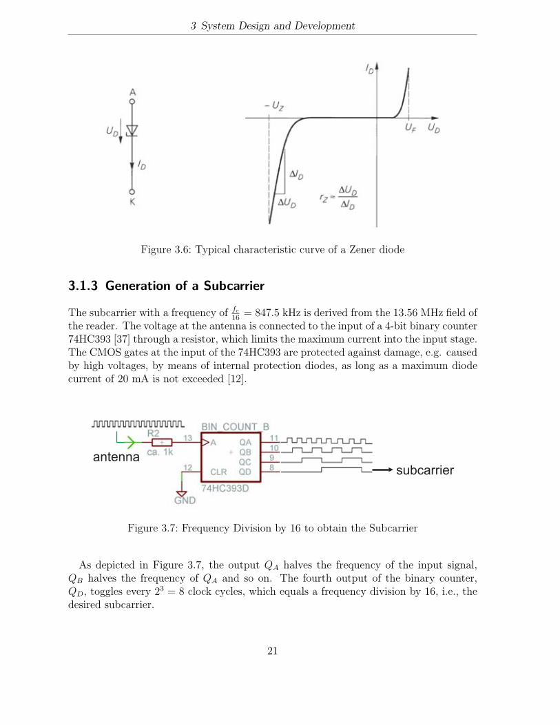
Figure 3.6: Typical characteristic curve of a Zener diode
3.1.3 Generation of a Subcarrier
The subcarrier with a frequency of fc
16= 847.5 kHz is derived from the 13.56 MHz field of
the reader. The voltage at the antenna is connected to the input of a 4-bit binary counter74HC393 [37] through a resistor, which limits the maximum current into the input stage.The CMOS gates at the input of the 74HC393 are protected against damage, e.g. causedby high voltages, by means of internal protection diodes, as long as a maximum diodecurrent of 20 mA is not exceeded [12].
Figure 3.7: Frequency Division by 16 to obtain the Subcarrier
As depicted in Figure 3.7, the output QA halves the frequency of the input signal,QB halves the frequency of QA and so on. The fourth output of the binary counter,QD, toggles every 23 = 8 clock cycles, which equals a frequency division by 16, i.e., thedesired subcarrier.
21

3 System Design and Development
3.1.4 Modulation with the Subcarrier
The modulation is achieved by ANDing the incoming Manchester coded signal withthe subcarrier, which is output by the frequency divider. As depicted in Figure 3.2,a common 74HC08 [39], containing four two-input AND gates, provides the resultingmodulated Manchester code at its output (compare with Figure 2.4). A pin-compatible7409 chip, providing open collector outputs and thus incorporating switching capability,might be used instead of the 7408, if the induced voltage level is kept small enough.
3.1.5 Load Modulation
A resistor has to be connected in parallel to the antenna of the tag to achieve (resis-tive) load modulation of the field generated by the reader, as described theoretically inSection 2.2.2.
Figure 3.8: Realisation of the switch for the load modulation
Figure 3.8 illustrates, how the aforementioned switch is realised with an IRFD 110 [20]n-channel MOSFET3, labeled with T1, allowing for fast switching and a maximum drain-source voltage of 100 V whilst having a low on-resistance of 0.54 Ω. A likewise fastSchottky diode, D1, in series with the adjustable load resistor R1, prevents the internalavalanche diode of the MOSFET from conducting during the negative half cycle of theHF field, when a negative voltage is applied between drain and source, which would leadto irreversible damage of the transistor. The output of the AND gate (see Section 3.1.5)is connected to the gate of the transistor, which will toggle the load resistor on, whenthe gate-source voltage exceeds approximately 3 V. Accordingly, the 848 kHz modulatedManchester code is modulated onto the 13.56 MHz field of the reader and the informationput into sidebands of the carrier frequency (compare with Figure 2.3).
Of course, as the n-channel transistor will only conduct when the voltage at theantenna is positive, load modulation only happens during one half cycle of the sine wave
3Metal-Oxide Semiconductor Field-Effect Transistor
22

3 System Design and Development
of the field. Still, good results were obtained with the described circuit. During thepauses, the field is completely switched off for full periods, while in the load modulationcase the amplitude at the antenna will rise again after one half cycle. So it is easier forthe fake tag to distinct between gaps in the field and load modulation.
3.1.6 Acquire Miller Pulses from the HF field
Figure 3.9: The adaptive envelope detector of the Fake Tag
The fake tag has to be able to distinguish between gaps in the HF field, caused by thereader sending data, and itself sending data, i.e. load-modulating the field. Furthermore,in addition to getting rid of the high frequent fraction of the field, a wide voltage rangeat the parallel LC-circuit must be handled, as the amplitude varies considerably withthe distance between the two coils. To achieve this goal, an LM 311 comparator [33]is used, combined with two envelope detectors at its inputs, as depicted in Figure 3.9,which are both connected in parallel to the antenna. The LM 311 is operated from thesingle 5 V supply present on the PCB and, wired with an appropriate pull up resistor,R4, at its output4, capable of producing appropriate 0 and 5 V levels.
During the positive half cycle of the field, the capacitors of the detectors are ratherquickly charged via the Schottky diodes. While the input at the diodes is negative, areverse flowing current is blocked, so that the capacitors can only discharge by means ofthe connected resistors.
The detector at the negative input of the comparator, formed by D1, C1 = 150 pF andR1 = 1 kΩ, is dimensioned for a fast response time and distinguishes between the field
4for fast reaction, during measurements a value of approximately 2.2 kΩ turned out to be optimal
23

3 System Design and Development
Figure 3.10: Fall times of the RC-circuits
being completely switched off and the load modulation case. With the time constantτ1 = 150 ns, derived in equation 3.8, a fall time of approximately 1.92 μs has beenmeasured, as depicted on the left of Figure 3.10. Note, that the capacitor dischargesso quickly, that the 13.56 MHz input signal from the antenna can be recognised in thewaveform.
τ1 = R1 · C1 = 1 kΩ · 150 pF = 150 ns (3.8)
τ2 = (R2 + R3) · C2 = (8.2 kΩ + 1.8 kΩ) · 220 nF = 2.2 ms (3.9)
The other envelope detector is formed by D2, C2 = 220 nF and the voltage dividerconsisting out of R2 = 8.2 kΩ in series to R3 = 1.8 kΩ. It has a rather large timeconstant of τ2 = 2.2 ms, calculated in equation 3.9, and averages the voltage at theantenna, which is then divided by a factor of 5.6, derived in equation 3.10, and then fedinto the positive input of the LM 311.
(R3
R2 + R3
)−1 = (1.8 kΩ
8.2 kΩ + 1.8 kΩ)−1 = 5.55 (3.10)
As shown in Figure 3.10 on the right side, for this RC-circuit, a fall time of approx-imately 4.5 ms has been measured. The resulting threshold voltage, appearing like aDC voltage during an established communication between reader and tag, is therebyadapted to the current field strength. This makes the circuit immune to noise caused bythe HF field, extends the operating range and ensures fast reaction to the gaps in thefield.
If the field is completely switched off, so that the voltage of the capacitor at theinverting input becomes smaller than the voltage at the non-inverting input, the outputof the comparator will become high, indicating the beginning of a gap in the field,illustrated in the left of Figure 3.11. Zooming into the waveforms, on the right side ofthe figure, a delay of only 545 ns can be observed, induced by the complete envelopedetection stage. The rise time of the output signal is slower compared to the fall time,originating in the open collector output of the LM 311.
24

3 System Design and Development
3.1.7 Pulsed Miller → Miller
The conversion of the pulses received from the reader to normal Miller code is necessaryto reduce the bandwidth needed for the transmission through the communication link(see Section 3.2.8). The output of the comparator is connected to the input of a positiveedge triggered 7474 D-type flip flop [41], whose inverted output is fed back into the Dinput, as depicted in Figure 3.12, leading to a change of the logic state at the outputon every rising edge occurring. The result of the obtained conversion from pulses intotransitions is called a Miller coded signal and wired to the communication interface, to beforwarded to the reader, where the pulses are reestablished and fed into the DIN input ofthe RF transceiver and an input pin of the microcontroller (compare with Section 3.2.4).
The power-on state of the flip flop is undefined, but this does not mean a problem,because, as illustrated in Figure 2.2, Miller coded bits are represented by transmissions,not by levels. The measured function of the stage is presented in Figure 3.13, where thevoltage of the antenna is on top, the acquired Miller pulses below, and the Miller codedsignal with a low bandwidth, for transmission over the communication channel, at thebottom.
Figure 3.11: Delay induced by the envelope detector
Figure 3.12: Conversion of Miller Pulses to normal Miller coded data
25

3 System Design and Development
Figure 3.13: Transformation of the signal between antenna and communication interface
3.1.8 Fake Tag Design Flow
The Coffee Cup Tag
To perform first tests, regarding the performance and tunability of a self made parallelresonant circuit for 13.56 MHz, and to develop an expedient circuit to achieve properload modulation, a simple but effective approach was chosen: A coffee cup, being thefirst obvious object at hand with the corresponding shape, was used to form a circularcoil, and other components were wired directly to it, as shown in Figure 3.14.
If the diameter d of the wire used is much smaller than the diameter of the coil, theapproximation in equation 3.11 can be used [15] for the calculation of the inductance Lof a circular conductor loop.
L = N2μ0R · ln(2R
d) (3.11)
The number of windings, N , was chosen equal to three, and the coated copper wireused has a diameter of d = 0.5 mm, while the radius of the coffee cup was found to beR = 40 mm. Inserting these values and the magnetic constant μ0 = 4π · 10−7 V s
Am, i.e.
the permeability of vacuum, into equation 3.11, results in the inductance of the copperwire coil calculated in equation 3.12.
L = 9 · 4π · 10−7 V s
Am· 40 · 10−3 m · ln(
2 · 40 · 10−3 m
5 · 10−4 m) = 2.3 μH (3.12)
The necessary parallel capacitor with a value of C = 59.9 pF, deduced from equation3.2, is realised as a fixed 47 pF ceramic capacitor in parallel to an adjustable one witha range from 4 pF to 30 pF, hence tuning to resonance is possible.
The Coffee Cup Tag turned out to be suitably tunable and was initially capableof performing load modulation with a subcarrier, i.e., the subcarrier could be either
26

3 System Design and Development
Figure 3.14: The Coffee Cup Tag
switched on or off, which then could be noticed at the amplitude of the measured fieldand at the signal at the DOUT pin of the reader (described below in Section 3.2).The form of the coil was later on fixed with superglue, to ensure mechanical long termstability.
The Fake Tag, Version 1
The Coffee Cup Tag was further extended with more components required for operation,resulting in a rather unconventional and unreliable appearance, depicted in Figure 3.15.
After testing several options for the circuit, the best variant was realised on a PCB,resulting in the first durable version of a device being able to emulate an ISO 14443compliant RFID transponder, termed Fake Tag, which is presented in Figure 3.16.
The inductance of the coil was determined to L = 1.25 μH, leading to a correspondingcapacitance of C = 110 pF, again realised as a 100 pF fixed capacitor in parallel to a6...30 pF variable capacitor. The one-sided layout, which was produced using the Layout
27

3 System Design and Development
Figure 3.15: Experimental extensions of the Coffee Cup Tag
Editor EAGLE 4.13 from CadSoft5, employs SMD6 technology to keep the dimensions ofthe device small, and the wires short, which is particularly important for high frequentsignals.
The Fake Tag, Version 2
For the second (and final) version of the Fake Tag, the complete circuitry is placed insideof the coil, thus achieving a larger coil area and longer operating range. Furthermore, asthis time a two-sided layout has been designed, the number of windings of the antennais doubled. Concerns about the strong magnetic field in the coil, potentially perturbingthe functional performance of the designed circuit, turned out to be baseless duringpertinent tests, if the integrated circuits are properly wired with bypass capacitors closeto their pins, to reduce the noise in the supply voltage.
The resistor for the load modulation is realised as a variable SMD type, and the sizeof the PCB is adapted to fit into a standard cigarette packet (shown on the right ofFigure 3.17), so that it can be easily hidden, e.g., during a real world relay attack.
For calculation of the inductance of the multilayer rectangular antenna, depicted inFigure 3.18, its spiral nature is neglected, i.e., the width and the height of the crosssection is assumed to be much smaller than the width and the length of the coil, so thatequation 3.13 can be used to find an estimation for the value of the inductance [26].Inserting the dimensions in cm, the inductance is obtained in μH.
5http://www.cadsoft.de6Surface Mounted Device
28

3 System Design and Development
Figure 3.16: The Fake Tag, version 1
Figure 3.17: The PCB of version 2 of the Fake Tag
29

3 System Design and Development
L =0.0276 · (CN)2
1.908C + 9b + 10h(3.13)
If w denotes the width and l the length of the coil, while b and h refer to the widthand the height of its cross-section, C in equation 3.13 is equal to C = w + l + 2h, i.e.,C = 5 cm+7.5 cm+2 · 0.1 cm= 12.7 cm. Accordingly, the second version of the FakeTag, with the number of turns N = 6, the height of the cross-section h = 0.1 cm andthe width of the cross-section b = 0.4 cm, has an inductance of L = 5.56 μH, as derivedin equation 3.14.
L =0.0276 · (12.7 cm · 6)2
1.908 · 12.7 cm + 9 · +10 · 0.1 cm)= 5.56μH (3.14)
Figure 3.18: Layout and dimensions of the Fake Tag, version 2
As above, the value of the capacitor to be connected in parallel, for a resonancefrequency of 13.56 MHz, is calculated from equation 3.2 and found to be approximatelyC ≈ 25 pF, so that a single adjustable (SMD-) capacitor of 6...30 pF should be sufficient.
30

3 System Design and Development
Figure 3.19: The Reader
3.2 The Reader
3.2.1 The RF Transceiver
The main part of the analogue front end is provided by the EM 4094 RF-transceiver7
from EM Microelectronics, which possesses a 200 mW push pull transmitter operatingat 13.56 MHz using an external quartz crystal, is capable of 100% ASK and ready forISO 14443A operation at a price of less than 5 e . According to the fact sheet [11],the device is also dedicated for operation compliant to the ISO 14443B or ISO 15693standards and provides interoperability with NFC devices. The received HF-Signal isdemodulated and can be conditioned by an internal 400 kHz to 1 MHz lowpass filter,a 100-, 200-, or 300 kHz highpass filter and selectable receiver gain, thus being able toprocess the required subcarrier frequency of 848 kHz (see Section 2.2.2).
The chip is well suited for the application described here, as its operation is trans-parent, i.e., a high input level on the DIN pin will instantly switch off the field, while alow level switches it on, enabling flexible, direct control of the RF field. The 848 kHzsignal received from the tag is output at the DOUT pin of the chip, from where it hasto be further processed before being treated, e.g., by the microcontroller described inSection 3.2.9.
Several option bits need to be programmed into the chip to set it up for the desiredoperation mode, which is done after every power-on by the microcontroller, via a threepin serial interface.
Unfortunately, to gain access to the full data sheet of the EM 4094, an NDA8 form,available from the website9, has to be filled in. Note, that both Melexis’ MLX90121 [31]and the S6700 Multi-Protocol Transceiver IC [47] from Texas Instruments offer possibil-
7transmitter and receiver8Non Disclosure Agreement9www.emmicroelectronics.com
31

3 System Design and Development
ities very similar to the EM 4094 and are therefore suitable replacements.
3.2.2 Impedance Matching
For convenience, the output stage of the chip has been matched to feed the signal into acommon 50 Ω coaxial cable, so different antennas can be tested by plugging them intothe SMA connector placed on the PCB10.
At the frequency of 13.56 MHz, the HF voltage has to be treated as an electromagneticwave, and undesired effects like power reflections have to be taken into account. Thereflection coefficient Γ, i.e., the ratio of the amplitude of the reflected wave to theincoming wave, is a measure for the reflected power. It can be derived from the outputimpedance of the source, ZL, and the characteristic impedance of the transmission lineconnected to it, Z0, according to equation 3.15.
Γ =ZL − Z0
ZL + Z0
(3.15)
For ZL being equal to Z0, the reflection coefficient will become zero, indicating thatno power is reflected back into the source. Accordingly, to minimise losses and achievethe maximum possible power transmission from the output stage of the reader into thecoaxial cable, the impedances have to be matched, which can be realised with a passivematching circuit using only a few components.
A method of visualising complex impedances and the corresponding reflection coeffi-cient is the so called Smith Chart [29], depicted in Figure 3.21, in which the entire righthalf plane of the complex impedance plane is mapped into a circle. Before drawing theinvolved impedances into the chart, they have to be normalised to the impedance ofthe transmission line, Z0 (which here equals 50 Ω), resulting in equation 3.16, where Z∗
L
denotes the normalised impedance of the source, i.e. Z∗L = ZL
Z0.
Γ =Z∗
L − 1
Z∗L + 1
(3.16)
In a Smith Chart, impedances connected in series can directly be added, while thoseconnected in parallel are obtained by adding the admittances, which are graphicallycreated by rotating the impedance by 180◦. The distance from the center of the chartto the outside of the circle is the reflection coefficient Γ, which is particularly convenientto perform impedance matching, as it is shown for the output stage in the followingsection.
3.2.3 The RF Output Stage
The output impedance of each of the antenna outputs ANT1 and ANT1 of the RFtransceiver is assumed to be resistive with 10 Ω each. To eliminate the DC component,
10Printed Circuit Board
32

3 System Design and Development
Figure 3.20: Schematic of the Output Stage
a 680 pF capacitor (C1 and C2 in Figure 3.20) is connected in series to each output,which at the frequency of 13.56 MHz results in an impedance equal to Z1, as derived inequation 3.17.
Z1 =(R1 + 1
jωC1) · (R2 + 1
jωC2)
(R1 + 1jωC1
) + (R2 + 1jωC2
)
=(10 Ω + 1
j·2π·13.56 MHz·680 pF) · (10 Ω + 1
j·2π·13.56 MHz·680 pF)
(10 Ω + 1j·2π·13.56 MHz·680 pF
) + (10 Ω + 1j·2π·13.56 MHz ·680 pF
)
= 5 − j · 8.6302 Ω (3.17)
The normalised impedance, i.e. Z1
50 Ω= 0.1− j · 0.173 Ω, is marked with an encircled 1
in Figure 3.21. An inductance of 285 nH is connected in series to obtain the impedancecalculated in equation 3.18, where the (parasitic) resistance of the coil, Ri = 0.45 Ω, istaken into account.
Ri + jωL = 0.45 Ω + j · 2π · 13.56 MHz · 285 nH = 0.45 + j · 24.28 Ω (3.18)
The normalised value, 0.009 + j · 0.486 Ω, is added to the impedance 1 in the SmithChart, to obtain the point marked with a 2, corresponding to a normalised impedance of0.109 + j · 0.313 Ω. To determine the total capacitance to be connected in parallel, nowthe admittance,labeled with 3, has to be taken by mirroring at the origin (dashed line inFigure 3.21). From here, the centre of the Smith Chart, where the reflection coefficientis Γ = 0, can obviously be reached by adding a normalised imaginary part of j · 2.85 Ω,corresponding to an overall capacitance Ctot = 669 pF.
33

3 System Design and Development
Figure 3.21: Impedance Matching with a Smith Chart
Reception Stage
During operation, due to resonance step up in the tuned circuit, peak to peak voltagesUAnt between 10 V and 15 V have been measured at the end of the antenna. As theamplitude at the RFIN input of the EM 4094, URFIN , must not exceed 5 V for properreception of the incoming signal, C4 and C5 in Figure 3.20 form a capacitive voltagedivider, through which the signal is fed into the RFIN pin.
URFIN =1
jωC5
1jωC4
+ 1jωC5
· UAnt =C4
C4 + C5
· UAnt
34

3 System Design and Development
=270 pF
270 pF + 510 pF· UAnt = 0.346 · UAnt (3.19)
As derived in equation 3.19, with C4 = 270 pF and C5 = 510 pF, the amplitude atthe input of the transceiver is reduced to a reasonable level of approximately one thirdof the antenna voltage, thus meeting the specifications of the transceiver.
The equivalent capacitance of C4 connected in series to C5 is calculated according toequation 3.20.
C4 · C5
C4 + C5
= 177 pF (3.20)
Hence, a further capacitance C3, with a value of 669 pF−177 pF≈ 490 pF, is to beconnected in parallel to obtain the total capacitance of Ctot = 669 pF, which is requiredfor the desired impedance matching, as derived in Section 3.2.3.
With the above described method, the impedances of the amplifier of the transceiverand the coaxial cable are made equal, and power is transmitted with almost no lossesthrough the waveguide to the antenna. There, a similar matching circuit is required, toadapt the antenna to 50 Ω. The required components can be found for each particularantenna, for example with the help of the Smith Chart, again.
3.2.4 Pulse Creation
In accordance to the ISO 14443A, pulses with a duration of approximately 2.5 μs have tobe created. This is achieved using a monostable multivibrator (monoflop) of the 74123type [42], wired with an external capacitor CEXT and a resistor REXT , whose values arecalculated after equation 3.21, out of the datasheet. In the equation, K is a voltagedependent constant, which, for a 5 V supply of the chip, is equal to 0.45, and tW standsfor the width of the output pulse.
tW = K · REXT · CEXT (3.21)
Hence, with CEXT = 2.2 nF and REXT = 2.7 kΩ, a pulse width of
tW = 0.45 · 2.7 kΩ · 2.2 nF = 2.67 μs (3.22)
is achieved.As depicted in Figure 3.22 , one half of a 74123 (containing two monoflops) is connected
to an output pin of the microcontroller. If it detects a rising edge at its input, a highpulse with the mentioned duration is emitted to the DIN input pin of the EM 4094,resulting in the field being switched off briefly. The workload for the microcontroller islessened this way, so it has some time, for example to prepare the next data to be sent.
Still, as there is also a direct connection from an output pin of the μC to the DINinput, different pulse widths are achievable, at the cost of more processing time by themicrocontroller.
35

3 System Design and Development
Figure 3.22: Wiring of the monoflop for generation of pulses
3.2.5 Miller → Pulsed Miller
Two more monoflops are utilised to convert the Miller coded data, received from thecommunication interface or generated by the microcontroller, into pulsed Miller codeddata, as depicted in Figure 2.2, which is again fed into the DIN pin of the transceiver.The inputs of two chips are wired in such a manner, that a transition of any type leadsto a pulse, as shown in Figure 3.23.
The pull-down resistor, required for an adequate low level at the output of the stage,can be found at the output of the monoflop in Figure 3.22, labeled with R11. The output(pin 13) of the monoflop can be treated as a virtual ground (while it is not emittingpulses), because the 74123 data sheet [42] specifies a maximum output sink current of25 mA, and the chip is therefore capable of pulling the left side of R11 close enough to0 V, in the context of the here developed circuit.
Figure 3.23: Recreation of pulses from the Miller coded input data
36

3 System Design and Development
3.2.6 Modulated Manchester → Manchester
The output at the DOUT pin of the EM 4094 is modulated with a 848 kHz subcarrier,making it difficult to acquire the data on the side of the Atmel and requiring a highbandwidth for the communication channel to the fake tag (see Section 3.2.8). To lowerthe bandwidth significantly and make it easier for the μC to perceive the data sent by thetag, the modulated Manchester code is demodulated, as explained below in this section.For further details and explanations regarding the schematic and corresponding signalwaveforms, please refer to Figure 3.25 and Figure 3.26, in which the whole demodulationprocess is illustrated.
Preparation of the DOUT Signal
Unfortunately, the output of the EM 4094 exhibits a non-ideal behaviour, as depictedin Figure 3.24. Deviant from the ideal waveform, the real signal may start with a highinstead of a low level, and the last pulse of each half bit cycle is elongated. If directlyfed into an envelope detector, the high level at the beginning of the non-ideal waveformwould misleadingly result in the circuit indicating a modulation being present, whilethe last elongated pulse would lead to a longer delay of the output signal and hencea displaced transition (which should be at the centre of the bit period, compare withSection 2.2.2).
Figure 3.24: Ideal and real signal at the DOUT pin of the EM4094 transceiver
The mentioned behaviour is accounted for by using another 74123 monoflop, labeledwith MONFLOP1B in Figure 3.25, which generates short pulses at every rising edge ofthe signal at the DOUT pin of the RF transceiver. With CEXT = 150 pF and REXT =5.6 kΩ, the pulse duration will be approximately 380 ns , as derived in equation 3.23.
tW = 0.45 · 5.6 kΩ · 150 pF = 378 ns (3.23)
Envelope Detection
The resulting waveform, labeled with 2 in Figure 3.26, is fed into a resistance-capacitancecircuit via a diode, similar to the envelope detection circuit of the Fake Tag, describedin Section 3.1.6. This time, as derived in equation 3.24, the voltage at the non-inverting
37

3 System Design and Development
input of the comparator, U+, is held on a constant level of ≈ 650 mV by a resistivevoltage divider formed out of R8 and R9.
U+ = 5 V · R9
R8 + R9
= 5 V · 1.5 kΩ
10 kΩ + 1.5 kΩ= 652.2 mV (3.24)
During simulations with PSpice, a time constant τman of the RC-circuit (R10 andC13 in Figure 3.25), as derived in equation 3.25, turned out to be the optimal trade-offbetween reliability and fast reaction time of the circuit.
τman = R10 · C13 = 2.2 kΩ · 470 pF ≈ 1 μs (3.25)
The corresponding signal for the voltage divider is labeled with a 4, while the voltageof the capacitor at the non-inverting input of the operational amplifier is marked witha 3 in Figures 3.25 and 3.26.
Figure 3.25: The envelope detector of the reader with surrounding circuitry
Depending on the voltage at the capacitor, an LM 311 voltage comparator [33] decides,whether the subcarrier is currently present or not, resulting in the output waveformlabeled with [5]. Having a closer look, a longer high time compared to the low time ofthe signal, caused by the above described demodulation process, can be noticed.
Signal Shaping
The mentioned uneven high and low time is corrected by the circuit following the com-parator, consisting out of a 7400 containing four two-input NAND gates [38], a variableresistor and a fixed capacitor. The signal coming in from the LM 311 is split up in twopaths, one of which leads directly to one of the two inputs of an AND gate, formed out oftwo NAND gates. The inputs of the remaining two NAND gates of the 7400 are shorted,thus acting as inverters, which ensure steep edges of the signal passing through them,
38

3 System Design and Development
while being delayed in between them by means of the RC-circuit, whose time constantτ can be adjusted with the variable resistor.
If a rising edge occurs at the input of the signal shaping stage, and therefore at oneof the two inputs of the AND gate, the output will not change, i.e., be kept low, untilthe signal from the delayed path arrives from the output of the second inverter. Bothinputs of the AND gate now being high, its output will eventually also become high,while the output level will at once change to low, if the incoming signal becomes low.
Hence, only the rising edge is delayed, whereas the point in time of the falling edgewill remain unchanged, at last resulting in the high time of the signal being shortenedby an adjustable amount, and, if properly set up, in normal Manchester encoded dataat the output of the demodulation stage, labeled with a 6 in Figure 3.26.
Figure 3.26: Step by step: Demodulation of the transceiver’s DOUT signal
Blocking the DOUT During Transmission
An undesired effect is, that the EM 4094 senses its own RF output, leading to a meaning-less signal at its DOUT pin during the transmission of data, which is not important fornormal reader operation, but would lead to a faulty performance during a relay attack,if it was forwarded to the fake tag.
The situation is depicted in Figure 3.27: While pauses are created in the RF field(waveform at the top), the DOUT output (waveform in the middle) toggles randomly.Preventing this vacant signal from being relayed is the task of the monoflop at the leftbottom of Figure 3.25, whose input is connected to the DIN pin of the EM 4094, thusemitting a high pulse with a duration of tblock ≈ 21 μs, according to equation 3.26, onoccurrence of a rising edge at the DIN pin.
tblock = 0.45 · R22 · C46 = 0.45 · 4.7 kΩ · 10 nF = 21.15 μs (3.26)
39
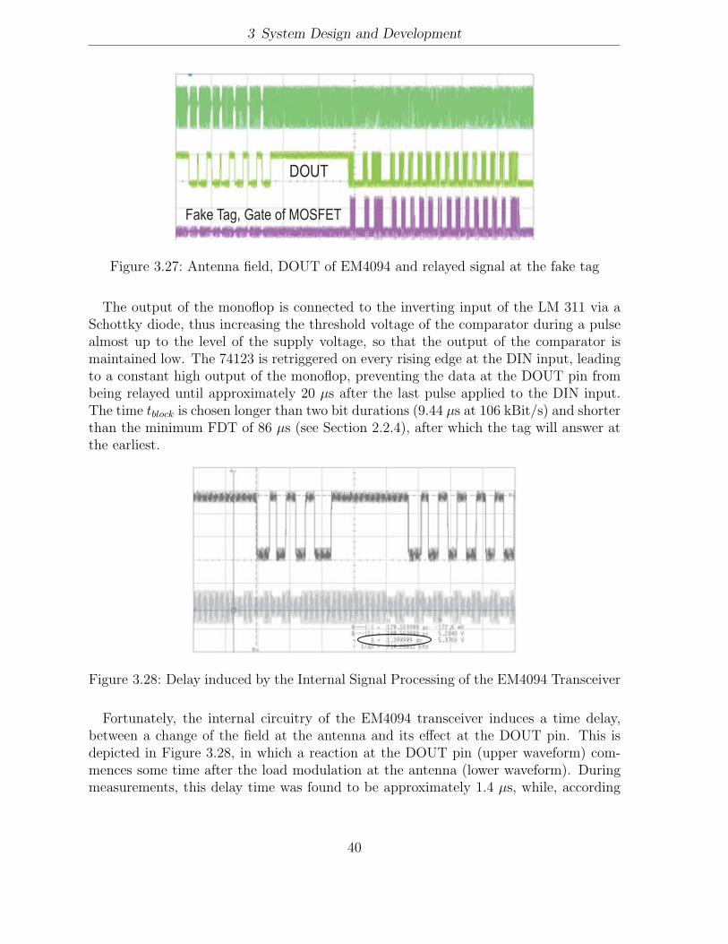
3 System Design and Development
Figure 3.27: Antenna field, DOUT of EM4094 and relayed signal at the fake tag
The output of the monoflop is connected to the inverting input of the LM 311 via aSchottky diode, thus increasing the threshold voltage of the comparator during a pulsealmost up to the level of the supply voltage, so that the output of the comparator ismaintained low. The 74123 is retriggered on every rising edge at the DIN input, leadingto a constant high output of the monoflop, preventing the data at the DOUT pin frombeing relayed until approximately 20 μs after the last pulse applied to the DIN input.The time tblock is chosen longer than two bit durations (9.44 μs at 106 kBit/s) and shorterthan the minimum FDT of 86 μs (see Section 2.2.4), after which the tag will answer atthe earliest.
Figure 3.28: Delay induced by the Internal Signal Processing of the EM4094 Transceiver
Fortunately, the internal circuitry of the EM4094 transceiver induces a time delay,between a change of the field at the antenna and its effect at the DOUT pin. This isdepicted in Figure 3.28, in which a reaction at the DOUT pin (upper waveform) com-mences some time after the load modulation at the antenna (lower waveform). Duringmeasurements, this delay time was found to be approximately 1.4 μs, while, according
40

3 System Design and Development
to the data sheet [42], the propagation delay of a 74HC123, between a rising edge at theinput and a pulse emerging at the output, is well below 100 ns, even under the worstconditions.
As the monoflop reacts much faster to the input data sent to the DIN pin, than theRF transceiver processes the information obtained from the field, relaying of the datafrom the DOUT pin to the fake tag is effectively blocked, long before the first impacts ofthe field being switched off are noticeable at the DOUT pin. The result can be surveyedin Figure 3.27 at the bottom, where, during a true working relay attack, no faulty signalis relayed to the gate of the transistor of the fake tag.
3.2.7 Extra Time Delay
As the demodulation of the signal received from the RF transceiver costs some time (inthis case ≈ 1.5 μs), it can happen, that the answer of the tag is not accepted whenbeing relayed to a remote reader (investigated in Section 4.3.1), because it is not wellsynchronised with the bit grid defined in Section 2.2.4.
Figure 3.29: Schematic of the Extra Delay
For this case a delay circuit, depicted in Figure 3.29, has been developed, with whicha short fixed time delay can be added to the outgoing signal, without altering thewaveform. The delay can be varied from 0 to approximately 7 μs by setting a jumperon the PCB, so that a point in time during the bit period of (106kBit
s)−1 = 9.44 μs can
be adjusted, for which the relayed answer of a tag is accepted as valid.The circuit consists of a 74HC74, containing six inverting Schmitt Triggers with a
typical hysteresis voltage of 0.9 V [41], combined with six resistor-capacitor pairs, eachhaving identical values. Due to the charging and discharging of the capacitor throughthe resistor, a time delay is created after every inverter. The optimal values, which are220 Ω for the resistors and 4.7 nF for the capacitors, were found during simulations per-formed with PSpice, such, that the maximum possible time delay was achieved withouta noticeable change of the waveform of the input signal. As the stages are connectedin series, the achieved time delay for the whole circuit is equal to the sum of the sixindividual delays.
In Figure 3.30, some results of the simulations are presented. The upper left graphshows the input and the (dashed) output signal of a typical Manchester encoded signal
41

3 System Design and Development
Figure 3.30: Simulation and Measured Performance of the Extra Delay
with a 106 kBit/s data rate. Below that, the voltages of the capacitors of every secondinverter, i.e. C1, C3 and C5 in Figure 3.29, are depicted. It is important, that thecapacitor of every stage is charged and discharged to the same voltage levels, so thatthe waveforms of each stage look identical, except for a shift in time. If this criteria isnot met, as will be the case for much larger values for the capacitors or resistors thanthe here chosen ones, the shape of the signal will be altered, e.g. the first pulse couldbe shortened.
By means of a jumper on the PCB (omitted in Figure 3.29), it is possible to choosebetween either no delay at all, i.e., bypass the extra time delay stage, or the signalpresent after the second (pin 4), the fourth (pin 8) or the last (pin 12) inverter of the74HC74. On the right of Figure 3.30, the input signal (at the bottom), and the delayedoutput signal (at the top), are depicted. Together with the time delay caused by otherparts of the developed circuit, e.g., the transceiver (see Figure 3.28) and the envelopedetector (see Section 3.2.6), an overall delay greater than one bit duration is achieved,so that the relayed data can be aligned to the bit grid defined in Section 2.2.4.
Figure 3.31: Manchester Coded Output of the Demodulation Stage
If the variable resistor of the signal shaping circuit, described in Section 3.2.6, is setup properly, an accurate Manchester encoded signal is obtained, as demonstrated inFigure 3.31, where both high and low time of the purposely delayed signal are found tobe equal.
42
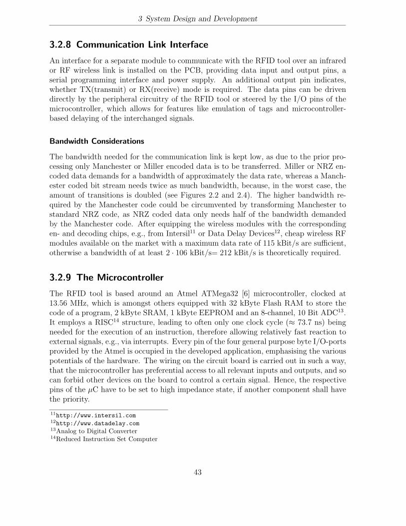
3 System Design and Development
3.2.8 Communication Link Interface
An interface for a separate module to communicate with the RFID tool over an infraredor RF wireless link is installed on the PCB, providing data input and output pins, aserial programming interface and power supply. An additional output pin indicates,whether TX(transmit) or RX(receive) mode is required. The data pins can be drivendirectly by the peripheral circuitry of the RFID tool or steered by the I/O pins of themicrocontroller, which allows for features like emulation of tags and microcontroller-based delaying of the interchanged signals.
Bandwidth Considerations
The bandwidth needed for the communication link is kept low, as due to the prior pro-cessing only Manchester or Miller encoded data is to be transferred. Miller or NRZ en-coded data demands for a bandwidth of approximately the data rate, whereas a Manch-ester coded bit stream needs twice as much bandwidth, because, in the worst case, theamount of transitions is doubled (see Figures 2.2 and 2.4). The higher bandwidth re-quired by the Manchester code could be circumvented by transforming Manchester tostandard NRZ code, as NRZ coded data only needs half of the bandwidth demandedby the Manchester code. After equipping the wireless modules with the correspondingen- and decoding chips, e.g., from Intersil11 or Data Delay Devices12, cheap wireless RFmodules available on the market with a maximum data rate of 115 kBit/s are sufficient,otherwise a bandwidth of at least 2 · 106 kBit/s= 212 kBit/s is theoretically required.
3.2.9 The Microcontroller
The RFID tool is based around an Atmel ATMega32 [6] microcontroller, clocked at13.56 MHz, which is amongst others equipped with 32 kByte Flash RAM to store thecode of a program, 2 kByte SRAM, 1 kByte EEPROM and an 8-channel, 10 Bit ADC13.It employs a RISC14 structure, leading to often only one clock cycle (≈ 73.7 ns) beingneeded for the execution of an instruction, therefore allowing relatively fast reaction toexternal signals, e.g., via interrupts. Every pin of the four general purpose byte I/O-portsprovided by the Atmel is occupied in the developed application, emphasising the variouspotentials of the hardware. The wiring on the circuit board is carried out in such a way,that the microcontroller has preferential access to all relevant inputs and outputs, and socan forbid other devices on the board to control a certain signal. Hence, the respectivepins of the μC have to be set to high impedance state, if another component shall havethe priority.
11http://www.intersil.com12http://www.datadelay.com13Analog to Digital Converter14Reduced Instruction Set Computer
43

3 System Design and Development
3.2.10 The Programming Adapter
For flexible operation and testing, the software running on the microcontroller can beupdated, without the need to remove it from the board, through a developed program-ming adapter, which is depicted in Figure 3.32 and can be plugged into the parallel portof a PC via the appropriate cable. The adapter is similar to the one described on thePonyProg2000 website15 and compatible to the widespread Atmel STK200 AVR StarterKit16.
Figure 3.32: The readily assembled program adapter
Measuring the voltage levels of parallel ports of various PCs, it turned out, thatsometimes a voltage of only approximately 3 V for a high logic level is delivered fromthe PC, which might not be accepted as a logic high by the (5 V-) CMOS compatibleAtmel. Therefore, a 74HCT244 [40], containing eight 3-state buffers, is inserted betweenthe parallel port and the appropriate pins of the ISP17 interface of the microcontroller,i.e. MOSI18, MISO19, SCK20 and Reset, to ensure adequate voltage levels for bothdirections. The schematic and the pin assignment for the cable to the parallel port of
15http://www.lancos.com/prog.html16available from http://www.kanda.com17In System Programming18Master Out Slave In19Master In Slave Out20Slave Clock
44
3 System Design and Development
Figure 3.33: Schematic of the program adapter
the PC is presented in Figure 3.33. Integrated circuits of the HCT type accept the lowerTTL21 levels at their inputs, while CMOS compatible levels are output [1]. Note, thatthree outputs of the 74HCT244 are connected in parallel, wired to the Reset pin of themicrocontroller, to achieve steep edges there. A red LED22 on the programming adapteris lit, if a program is being downloaded into the Flash memory of the Atmel.
3.2.11 USB Port
Fast communication with a PC or other USB equipped hardware is made possible bythe FT245R parallel to USB chip from FTDI23. The device allows to send or receivepackets of eight data bits, adequate to the 8-bit architecture of the microcontroller, bypulling a read or write input pin high and low, once a corresponding strobe pin indicateswhether the device is ready. Fetching or writing out one byte is possible in three clockcycles, as the minimum duration for a pulse to shift data from the input bus of thechip into the internal FIFO buffer is specified with 50 ns in the data sheet [16], which isautomatically met with one clock cycle of the microcontroller taking 75 ns. So, using thesupplied D2XX drivers, it is possible to exploit the maximum possible data transfer rate
21Transistor-Transistor-Logic22Light Emitting Diode23Future Technology Devices International – http://www.ftdichip.com
45
3 System Design and Development
of 1 Megabyte/second between the RFID tool and a PC. In addition, so called VCP24
drivers are available, providing access to the USB port as if it was a normal serial COMport, so that compability with programs implementing a normal serial port is given andany serial terminal program, e.g., Hyper Terminal25, can be utilised. During tests, aserial connection with a baud rate of 921600 bit/second has been established.
3.2.12 Design of the Reader – Approach and Hints
1st Version
After analysing the various capabilities of the I/O ports of the microcontroller, andchoosing the peripheral components described above, like the USB chip, the RF-transceiver,and more, a schematic for the first version of the reader was developed and entered intothe EAGLE Layout Editor, to create the layout, again using SMD technology wherepossible.
During the layout process, the packages of the devices used had to be matched tothe ones available on the market, and some new footprints had to be drawn and addedto the EAGLE libraries. Care had to be taken, where vias from the top layer to thebottom layer of the board were needed, as with the used “home-brew” technology, theconnection between the two layers is not achieved automatically after the etching ofthe PCB, but by afterwards soldering a little piece of wire, sticked through the board,for every via. This implicates, that vias are not possible in certain places, for exampleunder the socket for the microcontroller, where the wire can not be reached and heatedup properly with a soldering iron.
The dimensions of the reader are kept smaller than 80×100 mm, so that only half ofa standard 160×100 mm card is occupied. After transferring the layout onto a doublesided copper-clad board, coated with photo-resist, the PCB was etched and cut out.Afterwards, the holes for the vias and the other components were drilled and a thinplastic coating sprayed on the board, to protect it from corroding due to humidity. Theutilised “Plastik” spray from Cramolin26 turned out to be effortlessly solderable lateron, when the components were assembled. The result of the effort, the low level readerversion 1, is depicted in Figure 3.34.
For the power supply, a cheap unregulated mains adapter with a DC output voltageof approximately 7 to 9 V can be used and plugged into the DC socket on the board,as the voltage is regulated to constant 5 V by means of a 7805 voltage regulator, wiredaccording to the data sheet [32]. A reset of the microcontroller and hence the peripheraldevices can be triggered by means of a pushbutton on the board, as well as four LEDsand an additional pushbutton are provided for general user interaction.
24Virtual Com Port25Terminal program delivered with Microsoft Windows26http://www.cramolin.de
46

3 System Design and Development
Figure 3.34: The completely assembled first version of the reader
An on board RS 232-compliant serial interface to a PC is realised using a MAX 232RS 232 driver and receiver, wired amongst others with 1 μF electrolytic capacitors, asproposed in the data sheet [28]. With its internal voltage doublers and inverters, the 0or 5 V output levels of the RX / TX pins of the internal UART27 of the microcontrollerare translated to the approximately ± 8 V being necessary for the the RS 232 interface.
To ensure operating stability and reduce the influence of the HF field on the analogueand digital circuitry [48], for each device on the designed PCB at least one bypasscapacitor (often with a value of 100 nF) is placed as close as possible to the powerpins of the particular chip. This, of course, also applies to the developed Fake Tag (seeSection 3.1) and the program adapter (see Section 3.2.10).
The rather large DIP28 was chosen for the microcontroller, as it simplifies the layoutof the PCB29 and facilitates measurements, as a scope probe can be directly clampedto the pins of the device, thus making additional test pins unnecessary. As other SMDcomponents were placed underneath the chip, the increase in occupied board area isnegligible.
2nd Version
After the development of the first fake tag (described in Section 3.1.8) and successfullytesting the low level reader functionality, the labour was concentrated on the interactionbetween reader and fake tag. Working towards carrying out a relay attack, severalimprovements of the reader at hand became necessary, and were added to the circuitby means of discrete components. At the point, when the first relay attack had been
27Universal Asynchronous Receiver-Transmitter28Dual In-line Package29the pins of the chip are spaced far enough apart, so that connections can be made between them
47

3 System Design and Development
Figure 3.35: Experimental extensions of the first reader version
carried out successfully, these enhancements had grown to the freely wired and fairlyunreliable “piece of art” depicted in the right bottom corner of Figure 3.35, this makinga redesign inevitable.
All the components required for the extension of the reader were added to the ex-isting Eagle schematic, while the standard serial interface was omitted, as the USBinterface turned out to be an effective replacement. The outer dimensions of the PCBfor the second version of the reader, which is depicted in Figure 3.36, have been retainedunchanged, still being 80×100 mm.
3.3 Tuning the Antennas for Optimum Performance
For maximum operating range of both the reader and the Fake Tag, the respectiveantennas, some of which are depicted in Figure 4.7, have to be tuned to the presentcarrier frequency, matched to the input impedance, for example of a coaxial cable, andafterwards damped with a parallel resistor, to achieve the appropriate trade-off betweenbandwidth and amplitude.
48

3 System Design and Development
Figure 3.36: The PCB of the second version of the reader
Several tuning methods are proposed in the literature, for example in part 6 (testmethods for proximity cards) of the ISO 10373 [21], which are fairly complicated andrequire special equipment. Instead, the system was tuned with common sense, using theinstruments at hand, by the method described as follows.
The RF transceiver on the reader is used as a signal generator, set up to provide apure sine wave with the desired frequency of 13.56 MHz at the antenna output, whichwill be very precise, as originated from a crystal oscillator. The antenna to be tunedis plugged into the socket on the PCB and placed in a neutral environment (no metalsurfaces close to it, etc.). As depicted in Figure 3.37, a magnetic near field probe, whichis connected to an oscilloscope, is fixed at a position above the centre of the antenna,where the waveform on the screen of the scope is not distorted, i.e. a pure sine waveis obtained. The used circular probe is termed RF-R50-1 and part of the near fieldprobe set RF 230, manufactured by Langer EMV-Technik. Before the tuning processcan start, the characteristics of the parallel resonant circuit and the operation principleof the RFID system have to be taken into account.
The quality factor, Q, can be set by adjusting a variable resistor in parallel to the L andC of the particular resonant circuit. As described in Section 3.1.1, for higher Q factorsthe bandwidth becomes narrower, while, at the same time, the maximum amplitude atthe resonance frequency increases (compare with Figure 3.4). If the adjusted frequencyof a tuned circuit with a high Q is slightly displaced from the desired carrier frequency,a significant change of the amplitude of the field will be noticeable, whereas for a low Q,
30http://www.langer-emv.de/en/produkte/prod_rf2.htm
49
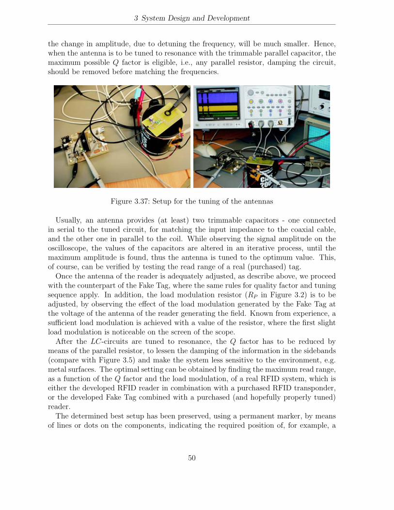
3 System Design and Development
the change in amplitude, due to detuning the frequency, will be much smaller. Hence,when the antenna is to be tuned to resonance with the trimmable parallel capacitor, themaximum possible Q factor is eligible, i.e., any parallel resistor, damping the circuit,should be removed before matching the frequencies.
Figure 3.37: Setup for the tuning of the antennas
Usually, an antenna provides (at least) two trimmable capacitors - one connectedin serial to the tuned circuit, for matching the input impedance to the coaxial cable,and the other one in parallel to the coil. While observing the signal amplitude on theoscilloscope, the values of the capacitors are altered in an iterative process, until themaximum amplitude is found, thus the antenna is tuned to the optimum value. This,of course, can be verified by testing the read range of a real (purchased) tag.
Once the antenna of the reader is adequately adjusted, as describe above, we proceedwith the counterpart of the Fake Tag, where the same rules for quality factor and tuningsequence apply. In addition, the load modulation resistor (RP in Figure 3.2) is to beadjusted, by observing the effect of the load modulation generated by the Fake Tag atthe voltage of the antenna of the reader generating the field. Known from experience, asufficient load modulation is achieved with a value of the resistor, where the first slightload modulation is noticeable on the screen of the scope.
After the LC-circuits are tuned to resonance, the Q factor has to be reduced bymeans of the parallel resistor, to lessen the damping of the information in the sidebands(compare with Figure 3.5) and make the system less sensitive to the environment, e.g.metal surfaces. The optimal setting can be obtained by finding the maximum read range,as a function of the Q factor and the load modulation, of a real RFID system, which iseither the developed RFID reader in combination with a purchased RFID transponder,or the developed Fake Tag combined with a purchased (and hopefully properly tuned)reader.
The determined best setup has been preserved, using a permanent marker, by meansof lines or dots on the components, indicating the required position of, for example, a
50

3 System Design and Development
trimmable capacitor.
3.4 Software
In this section, an overview of the used programs and the interaction between the de-veloped libraries and functions is given. The source code (see appendix) is commentedin detail, so that it should be no problem to understand the concrete implementation,or conclude to the task of the not mentioned operations.
The developed software for the Atmel AVR microcontroller is mostly written in C31
and compiled with the free avr-gcc compiler32. Some of the currently implementedfunctions are listed below.
• set up and control the EM 4094 RF transceiver,
• receive and send data via the USB port,
• precise wait/delay function,
• implementation of standard and short frames, including parity bit generation, asspecified in ISO14443, part 3,
• generation and sending of Manchester coded data = tag emulation,
• generation and sending of Miller coded data = reader functionality,
• the user can switch between the operating modes like relay, tag emulation or readermode.
3.4.1 Development Tools
The free WinAVR development environment33 consisting of compiler, linker, librariesfor various Atmel microcontrollers and an editor, called “Programmers Notepad”, wasfound to be very helpful for comfortable programming and editing of the program code.
A so called Makefile has been created, with all the parameters necessary for theproduction of binary (.hex) files out of the C code, such as the microcontroller type, theprocessor frequency and the name of the file containing the required main() routine.The editor allows user defined tools to be implemented in the environment, so thatcompiling, linking and fast downloading of the binary file to the μC, with the help ofthe Makefile, is effectively done by just one keystroke.
31parts in (inline) assembler32http://www.avrfreaks.net/AVRGCC33http://sourceforge.net/projects/winavr
51

3 System Design and Development
The AVRStudio Integrated Development Environment34, available from the Atmelwebsite35, was found to be suitable for debugging purposes, for example by disassemblingthe generated code and analysing it with respect to the clock cycles needed for theexecution. Furthermore, all the internal registers of the Atmel, as well as the I/O-ports,can be observed and arbitrarily modified.
Some options of the microcontroller, such as the clock source or whether a bootloader is used, have to be set by programming so-called flash fuses of the μC. Thiscan be done with the PonyProg200036 by choosing “Configuration and Security Bits”from the “Command” menu. Previously, the “Interface Setup” has to be altered to“AVR ISP I/O”, and the correct microcontroller type, i.e., AVR micro ATMega32,has to be selected. Note that for all fuses, “0” means programmed, while “1” meansunprogrammed, as described in the data sheet [6]. The optimal setting for the Atmelon the reader board is, to leave all options unchecked in the PonyProg program, exceptfor CKOPT, BOOTSZ1 and BOOTSZ0.
3.4.2 Description of the Source Code
For convenience, the code is separated into several files, the contents of which are de-scribed below. More details about the internal structure of the Atmel ATMega32 canbe found in the data sheet [6].
board.h
A header file board.h contains macros, declarations of variables and prototypes of func-tions, which are needed by the other libraries or the main program. Note, that variablesor functions declared in the header file still have to be defined elsewhere - the declarationjust ensures global access.
Worth mentioning is the definition of the global flags, which are stored in a bit-accessible I/O location of the μC, in this case the otherwise unused EEDR data registerfor the EEPROM. Setting or polling a flag placed in a bit-accessible location takes onlyone clock cycle, thus saving execution time, which is especially important for the realtime processing of data in an ISR37. Currently, only two flags are employed: ISRBusy
indicates, whether a particular ISR is finished with the processing of the current data.The other flag, IsPause, is used to hand over the current data to be sent to a ISR.
34IDE35www.atmel.com36http://www.lancos.com37Interrupt Service Routine
52
3 System Design and Development
em4094lib.c
The library em4094.lib was developed for controlling the EM 4094 chip and further-more encoding and preparing the data to be sent, according to the ISO 14443. CallingEM_Init() results in the DDRs38 of the pins of the Atmel, which are connected to theRF transceiver and the communication interface, being properly set. The EM 4094 isenabled, reset and then initialised (by means of other developed functions) with the ap-propriate option bits for ISO 14443 compliant operation. For comfortable programming,defines have been implemented for the most often used pins, e.g., a DIN_LOW; pulls thecorresponding pin low and a DIN_HIGH; sets it to a high level.
Care has to be taken with regard to the data direction (input/output) of the DIN pin.During the initialisation process, the DIN pin is directly driven by the μC, and thereforeused as an output. Later on, the pulses necessary for sending data are generated by anexternal device (see Section 3.2.4), so that the pin defined as DIN_PULSE is utilised. Thisimplies, that the DIN pin has to be set to tri-state, i.e., input direction, as otherwise twooutputs will try to drive the DIN pin simultaneously, which might damage the devicesand is counterproductive to sending out valid data. This has to be done “manually” inthe main routine, depending on the desired functionality.
After the initialisation, the three timers of the microcontroller are set up with therespective values. The (8-bit-)timer 0 is used, when Miller coded data is to be output.Timer 1, with 16 bit resolution, is utilised in the context of a wait-routine, when a longer,but still exact, pause is required (e.g., the FDT after sending out a REQA command).Timer 2, an 8-bit-timer again, is used for sending out Manchester encoded data, and,like timer 1, is set up for sending out data at a rate of 106 kBit/s. As the microcontrolleris clocked with 13.56 MHz, and the data rate is derived from this frequency, the timingof the resulting data output is very accurate.
Efforts to encode the data from NRZ to Miller or Manchester code in real-time, bymeans of implementing a state machine in the ISRs, have turned out to be unavailing.As every register of the Atmel used in an ISR has to be pushed on the stack39 beforeits execution, the extra time needed for the whole process does by far exceed the only64 clock cycles until to the next call of the ISR, under any circumstances. Hence, theprogram had to be optimised for execution speed during the transmission of data, atthe cost of memory40 usage, and a sequence for pre-processing the data, described forsending out Miller coded frames41, as follows, has to be obeyed.
First, the data to be sent is handed over to the function EM_SendShortFrame orEM_SendStandardFrame, depending on the kind of frame to be sent (see ISO 14443 [22],part 3). The seven bits needed for a short frame are passed over in the form of a byte,
38Data Direction Register39and later on popped off the stack again40there is plenty of memory available on the ATMega32 µC41The principle and names of the functions are similar for Manchester coded data
53

3 System Design and Development
where the MSB42 is ignored and the LSB is sent first. For a standard frame, data isinterchanged in the form of a pointer to an array, where the first byte in the array is sentfirst. The mentioned functions convert the data into the respective format of the framesand store the result in an array termed Frame2Send, in which the data is represented aslisted below (compare to Section 2.2).
0 = SOC, 1 = One, 2 = Zero, 3 = EOC
Note that, as the EOC of Miller encoded data consists out of two bytes, with the firstbyte being equal to a logic 0, the EOC above corresponds to the second byte.
The (odd) parity bit for each data byte, needed for the creation of standard frames,is returned by the EM_Parity function:
uint8_t EM_Parity(uint8_t byte, uint8_t mode)
// returns Parity bit for odd(mode=1) or even(mode=0) parity
{
byte ^= (byte >> 4);
byte ^= (byte >> 2);
byte ^= (byte >> 1);
byte &= 1; //now byte contains the bit to add for EVEN number of ones
return (byte^mode);
}
The parity is effectively calculated as shown above, by XORing one bit with every otherbit, which is the same as a modulo 2 addition of each bit of the data [35]. Please bearin mind, that a zero is coded as a “2” in the Frame2Send array, while the parity routinereturns a “0”.
In the next step, by means of the function EM_DoTheMiller, the data is encoded asrequired by the ISO 14443 standard, in such a way, that one byte in the array representsone half period of a bit to be sent, and thus the ISRs can effectively shift the data tothe DIN pin of the chip. This “waste” of memory has been necessary due to the internal8-bit structure of the microcontroller, which causes accessing a bit in the memory to takelonger than accessing a byte. In the current implementation, insertion of an additionalNOP43 in the corresponding ISR, taking one clock cycle for execution, already leads, inthe worst case, to invalid data being transmitted, because the pointer to the Frame2Sendarray has not been increased (as required for proper operation) before the subsequentcall of the ISR.
A call of EM_SendMiller sets up the timer, such that the ISR is called every halfbit period, i.e., 4.72 μs at a data rate of 106 kBit/s, and activates the correspondentinterrupt, so that at last the data is forwarded to the RF transceiver, as follows.
42Most Significant Bit43No Operation (computer processor instruction)
54

3 System Design and Development
1. get the current value from the Frame2Send array
2. increase the pointer to the Frame2Send array
3. set the IsPause flag, according to the current value
4. set the ISRBusy flag to 1
5. wait for the ISRBusy flag to become 0, indicating that the ISR has finished trans-ferring of the current data
6. proceed with 1 until all data is sent.
Simultaneously, the ISR of timer 0 is executed on every timer overflow occurring,simply performing the below listed operations.
1. if the IsPause flag is set, trigger a pulse at the DIN input of the RF transceiver
2. clear the ISRBusy flag
After all the data is sent out, the interrupt is deactivated again, to not disturb theother duties of the program.
ftlib.c
The library ftlib.c provides definitions, macros and functions for controlling of theFT 245R USB chip, and thus the interface for data transmission from and to the PC.One port of the microcontroller is connected to the eight data input/output pins of theFT 245R, while four more pins are needed to switch between reception or transmissionof data, and for handshaking purposes.
The data to be sent or received is stored in an array termed USBData. An examplefor a macro definition, used to acquire data from the USB chip, is given below:
#define FT_READ(Pointer) RD_LOW; USBData[Pointer++]=FT_DATA_PIN; RD_HIGH
Issueing the command FT_READ(CurrentByte); in a function thus results in the datacurrently present at the FT_DATA_PORT being stored to the position in the USBData array,where CurrentByte points to, and in increasing CurrentByte afterwards.
The function FT_Init has to be called once to initialise the directions of the pinsneeded for communication and enable the internal pull up resistors of the μC, wherenecessary. Before the first call of the FT_Send function, to send an array of data bytesto the USB port, the FT_WR_PIN has to be pulled low. A similar pre-condition appliesto the FT_Send function, for which the FT_RD_PIN is to be set to high before the firstexecution. The number of received bytes in the USBData array is returned, when all datais received from the PC, which is detected by occurrence of a time-out44 of the timer 1.
44currently set to approximately 1 ms
55
3 System Design and Development
etcetera.c
The serial port (only available in the reader version 1) is set up and controlled via severalfunctions in the etcetera.c library45. Furthermore, a function ETC_CheckButton() isprovided, which returns a value different from zero, if the push-button on the PCBwas pressed down in the moment of its execution. The pins of the microcontrollerconnected to the LEDs on the reader are set up by calling ETC_InitLEDs(). Pulling thecorresponding pin of the Atmel low results in the LED being switched on.
test.c
For testing of the so far implemented functions, a test.c program, containing the main()routine, was written. After calling the initialisation routines of the other libraries, de-scribed above, an endless loop is executed, in which a user interaction can take place.
If the reader is connected to a PC via USB, and the FTDI USB VCP driver is properlyinstalled (see Section 3.2.11), a serial terminal program can be used to establish a con-nection with a baud rate up to 921600 bit/second. After triggering a reset via the resetpush-button on the board, the reader will announce his presence by issueing a “Hello!”and the current state, which is the listening mode after a reset. By pressing a key, theuser can change between several operation modes, which are listed below.
• ’l’ - Listen mode - needed to for performing a relay attack or to acquire data
• ’r’ - A REQ is instantly sent out
• ’w’ - A WUP is instantly sent out
• ’a’ - The reader waits for an incoming command from the Fake Tag. After a fixedtime, an ATQ is sent out to the Fake Tag, confirmed by an “ATQ sent.” via theUSB port.
• ’t’ - likewise to ’a’, but the delay time is increased each time ’t’ is pressed, and thevalue handed over to the wait routine is output via the USB port.
The chosen state is indicated by different LEDs being lit on the PCB and by the outputof the reader in the terminal program.
45see comments in the C code for a description
56

4 Applications and Results
4.1 Low Level Reader
Figure 4.1: Testing the Low Level Reader with a German e-passport
The flexible low level reader function has been successfully tested with several ISO 14443compliant tags, which all answered to the commands sent out by the reader. Figure 4.1shows the measurement setup for tests with an electronic passport, issued by the FederalRepublic of Germany, at the moment of the passport sending out an ATQA. A PCBtype antenna serves as the coupling element to the antenna of the ISO 14443 chip, whichwas found to be embedded in the cover of the passport. On the top of the screen ofthe oscilloscope, the generated load modulation generated can be spotted in the field,which is measured by the magnetic near field probe in front of the picture. Below thewaveform of the field is the modulated Manchester code at the DOUT output of the
57
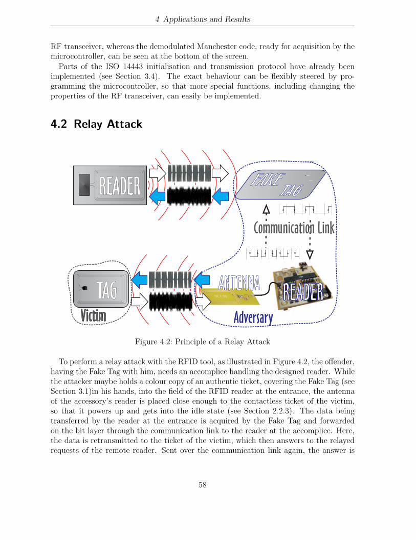
4 Applications and Results
RF transceiver, whereas the demodulated Manchester code, ready for acquisition by themicrocontroller, can be seen at the bottom of the screen.
Parts of the ISO 14443 initialisation and transmission protocol have already beenimplemented (see Section 3.4). The exact behaviour can be flexibly steered by pro-gramming the microcontroller, so that more special functions, including changing theproperties of the RF transceiver, can easily be implemented.
4.2 Relay Attack
Figure 4.2: Principle of a Relay Attack
To perform a relay attack with the RFID tool, as illustrated in Figure 4.2, the offender,having the Fake Tag with him, needs an accomplice handling the designed reader. Whilethe attacker maybe holds a colour copy of an authentic ticket, covering the Fake Tag (seeSection 3.1)in his hands, into the field of the RFID reader at the entrance, the antennaof the accessory’s reader is placed close enough to the contactless ticket of the victim,so that it powers up and gets into the idle state (see Section 2.2.3). The data beingtransferred by the reader at the entrance is acquired by the Fake Tag and forwardedon the bit layer through the communication link to the reader at the accomplice. Here,the data is retransmitted to the ticket of the victim, which then answers to the relayedrequests of the remote reader. Sent over the communication link again, the answer is
58

4 Applications and Results
relayed back via the fake tag to the reader at the entrance. As the exchanged data isfurther on relayed, both remote reader and the transponder in the ticket of the victimwill be convinced, that they are in close vicinity to each other and share the same secret.After less than one second, the entrance could open up and the attacker gain access toa restricted area, without allowance.
A relay attack, as described above, has been successfully carried out using the devel-oped tool with
• a digital passport (e-passport), issued in January 2006 by the Federal Republic ofGermany, with an ISO 14443 chip in its cover,
• an ISO 14443 compliant student identity chip card employed for payments at theRuhr-University in Bochum,
• Philips standard (classic) Mifare and DESFire cryptographically enabled smart-cards,
• an Atmel AT88SC153 contactless smartcard,
• and tickets for the FIFA World Cup 2006 in Germany,
until to the point of at least reading out the UID (see Section 2.2.3) of the tags andfurthermore, in the case of the Mifare classic, until to successful login to the card.
The assembly for executing a relay attack with the designed hardware is depicted inFigure 4.3. On the left of the picture, a ticket for the world championship is placedupright on the chair, with an antenna in front of it, which is establishing the RF connec-tion between the developed reader and the tag implanted in the paper of the ticket. Theso-called smart label, which is a combination of chip and antenna being manufacturedthin enough to be embedded in paper, becomes visible, if the ticket is exposed to asource of light from behind, as demonstrated1 in Figure 4.4. The reader is connectedto the Fake Tag, which is positioned on top of a proprietary reader (in the right topcorner of the picture), via a cable. With this reader, all 64 bytes stored on the MifareUltralight Chip (see Section 4.2.1) were successfully read out remotely, with the relaymode of the RFID tool, thus proving that the proprietary reader takes the Fake Tag asan authentic one.
The minimum overall delay induced by the depicted assembly, in the case of the readerbeing directly connected to the Fake Tag by means of a wire, is approximately 2 μs.
4.2.1 World Cup Ticket Remarks
It turned out, that a Philips Mifare Ultralight chip is embedded in the ticket [45],providing no encryption at all, so that in reality a relay attack is not necessary for an
1for protection of privacy, the personal data printed on the ticket has been altered
59

4 Applications and Results
Figure 4.3: Relaying a ticket for the world championship
offender to spoof the RFID access control. Instead, a replay attack can be performed,the principle of which is much easier. The contents of a ticket, which in case of the MifareUltralight chip is the UID and a maximum of 64 bytes, which are stored in 16 blocks,have to be read out and stored in the memory of the microcontroller, by means of thedeveloped reader2. The communication protocol, which would have to be implementedfor the attack, is fully published in the data sheet [44]. At a crowded place or in aqueue, where the short operating distance of the system can be achieved, the contents ofseveral tickets could thus be recorded. At the entrance, where an RFID reader examinesthe content of the smart labels, the data of a ticket can be replayed via the Fake Tag,making the reader believe to have a valid ticket in its vicinity.
The security of this particular RFID ticketing system probably relies on the fact, thatthe fixed UID of the employed chip is usually determined during manufacturing of thesmart label and cannot be changed later on. A combination of the UID with the datastored on the ticket will very likely refer to the entry of the purchaser of the ticket in adata base. Fortunately, the emulation of both the data stored on the smart label and theUID is effortlessly possible with the developed tool, thus making such a simple attack
2stand-alone operation without connection to a PC is possible
60

4 Applications and Results
feasible. Hence, from my point of view, no security at all is provided by the describedsystem.
Of course, tracking movements of individuals in the stadium, by means of their tickets,is possible, due to the fixed UID.
Figure 4.4: Sunlight from behind reveals the secrets of the world championship ticket
4.2.2 Timing
When performing a relay attack, an extra delay induced by the processing of the signal isinevitable. In practice, the minimum arising time delay will be one bit slice, as definedin Section 2.2.4, which is confirmed in Figure 4.5, where the FDT between a REQAcommand of the reader and the ATQA answer of the tag during a working relay attackis depicted. The first edge of the answer of the transponder, in the middle of the figure,occurs approximately 95 μs after the last gap in the field of a proprietary reader, on topof the figure, which corresponds to the mentioned bit slice duration.
Even if the reader scrutinised the timing requirements demanded by the ISO stan-dard during the initialisation phase (see Section 2.2.4), the attack could be carried outsuccessfully, as the (fixed) bit sequence of an ATQA command could be stored on theμC and then sent out fast enough after an incoming REQA request, to meet the timingspecification.
4.2.3 Implications on Privacy and Security
Employing ISO 14443 RFID tags in security sensitive applications should be regardedvery critically, as the assumption of the contactless interface being secure, i.e., resistantto relay attacks, is proven to be wrong. The card identified by a reader does not have to
61

4 Applications and Results
Figure 4.5: Induced delay during a relay attack
be in the direct vicinity of the reader, as declared by many manufacturers, but can beelsewhere and its data relayed from large distances without the permission of the owner.More endeavours have to be made to enhance the security of the interface, apart fromlimiting the reading range3 to 4 cm [3].
When security or privacy is necessary, an ISO 14443 compliant RFID transpondershould not be able to become active until the owner has performed a certain action,i.e. press a button or open the cover of his e-passport, as this would almost eliminatethe possibility of performing a relay attack.
4.3 Timing Analysis of a Commercial RFID reader
4.3.1 Tag Emulation Measurements
Using the tag emulation mode of the RFID tool, timing measurements have been per-formed with an ACG4 Dual 2.1 passport reader module. The ATQA answer of thedeveloped fake tag to a REQA issued by the ACG reader was intentionally delayed andthe reaction of the reader, i.e. if the answer was accepted as valid or not, was analysed.The ISO 14443 requires the tag to answer after exactly 86.9 μs.
4.3.2 Results
As presented in Figure 4.6, the Fake Tag was not only recognised as an authentic tag, butits ATQA answer accepted as valid, even after more than 200 μs. Every 9.44 μs, which isequal to one bit period of the 106 kBit/s data rate, during a time-slice of approximately2.5 μs, the answer of the tag was repeatedly accepted. Compliance with the strict timing
3anyway being a contradiction to just waving a credit card to carry out payments, as advertised4http://www.acg.de
62

4 Applications and Results
Figure 4.6: Measured behaviour of the ACG reader
requirements of the ISO 14443 (see Section 2.2.4 above) during the initialisation phasecould not be observed, thus facilitating relay attacks (see Section 4.2).
4.4 Antenna Tests
Various kinds of antennas were built, as depicted in Figure 4.7, some layouted on a PCBas proposed in an application report [49], as well as self developed ones made out of thincopper wire. They were tuned to resonance with the carrier frequency of the reader andto the 50 Ω coaxial cable, and tested with regard to operating range and the influenceof different environments.
It turned out, that the tuning can significantly alter the read range of the low levelreader. Sometimes longer distances were achieved, when the antenna of the readerwas slightly detuned. During tests with a 60×30 mm rectangular PCB antenna, for oneparticular setting of the trimmable capacitors, a read range from 0 to 5 cm was achieved,i.e. the contactless smartcard could be placed directly on top of the antenna. When theantenna was tuned for greater read ranges of approximately 10 cm, the card had to beplaced at least 3-5 cm away from the antenna for successful communication – placing thecard directly above the antenna, in this case, resulted in no valid data being acquiredby the RF transceiver.
To be able to compare the achieved maximum and minimum ranges, also as a functionof the tuning, the antenna of the reader was put on the table, and the smartcard withthe transponder was positioned above it by means of a tripod, as depicted in Figure 4.8.The achieved read ranges were read off the scale of a ruler, also fixed to the table.
The achieved operating range is best, if the antenna size of the tag matches thedimensions of the antenna of the reader, and the antennas are properly aligned to each
63

4 Applications and Results
Figure 4.7: Wire and PCB antennas with different dimensions
other, seemingly as then the best inductive coupling is achieved.
4.4.1 Enhance Privacy Protection
Placing the antenna above a metal surface resulted in noticeable decreased field strength,i.e., reading range. Further investigations showed, that aluminum foil shields the deviceand so protects it from being reached by an unauthorised reader. A single layer of foilwrapped around a tag completely prevents reading out its data, this therefore being anappropriate countermeasure against relay attacks.
One might have the idea of putting only one slice of metal foil in his purse, close towhere the contactless card is, i.e., shield the tag from only one side. This results in thereading range being only slightly (approximately 10 %) decreased, thus not providingsecure protection.
64
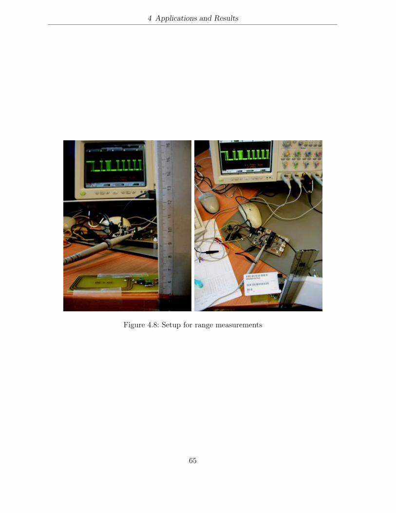
4 Applications and Results
Figure 4.8: Setup for range measurements
65

5 Future Prospects
Before realising any new improvements or enhancements, the produced circuit boardsof the second version of the reader and the Fake Tag should be assembled with thecomponents1 and tested, as more reliable operation is expected on the long run. Ifwireless RF communication between Fake Tag and reader is desired, suitable wirelessmodules can be purchased from Semtech2 (e.g., the DP 1205 drop-in RF transceivermodule), Radiotronix3 and other companies. For a simplified development of embeddedsystems in the future, versions of the layouts and schematics are existing, in which thefragments of the designed circuit, e.g., voltage regulation, μC or RF transceiver, areseparated from each other.
The current software has to be adapted to the new hardware, as several connectionsto the microcontroller have changed, i.e., other pins and ports are used for certain sig-nals. Furthermore, the program on the microcontroller should be extended for acquiringManchester and Miller coded data, and shifting it over to the PC in real-time. Theusage of so-called anticollision frames, as defined in the ISO 14443, may be requiredfor some commands during the initialisation phase of the transmission protocol. Anexample algorithm, written in C, for the generation of a CRC-16 checksum, which isnecessary for these frames, can be found in part 3, annex B of the standard [22].
If a synchronous operation of the microcontroller with the field generated by the RFtransceiver is desired, a 13.56 MHz signal can be utilised, which is provided at theDOUT1 output of the EM 4094 during reception of data from an RFID tag. Beforebeing fed into a ”‘Counter Clock Source”’ pin of the μC, the frequency of the signalis divided by 16 (compare with Section 3.1.3), thus being slow enough to serve as theexternal clock for the counter T0 of the Atmel.
5.1 Improved Man in the Middle Attack
5.1.1 Data Logging
As, in the first place, the μC is not needed for a relay attack (see Section 4.2), it maybe used for logging the data interchanged between tag and reader. All that has to bedone, is to reprogram the microcontroller with the appropriate software, because all the
1which have already been purchased2www.semtech.com3www.radiotronix.com
66

5 Future Prospects
required signals are already interconnected. The recorded data can be sent over the USBport to a PC or other cryptographic hardware. This can be helpful to come to knowabout proprietary, not publicised protocols, as well as to store the acquired informationfor further processing and analyses, such as key-search with cost-effective hardware [25].
5.1.2 Active MITM
Furthermore, the μC could perform an active task by adding an extra delay to thesignals or modify the data relayed → an active man-in-the-middle attack. During theinitialisation, the induced time delay could be eliminated, as described in Section 4.2.2,by replaying previously stored commands, instead of the “real” relayed answer of thetag, at a desired point in time after the request of the reader.
With little effort, higher data rates than 106 kBit/s could be circumvented, by sendingcounterfeited data packets at the appropriate point of the protocol, where reader andtag agree about the transmission speed, which will usually happen at an early stage ofthe particular protocol, where the data is still unencrypted.
Altering data of an encrypted information exchange is lot harder and only a theoret-ical construct, even with the help of specialised cryptographic hardware. The key forencryption of the current session would have to be found out by the attacker in real-time,so that the acquired data could be decrypted, altered, and then encrypted again, beforebeing relayed. If state-of-the-art cryptography is employed, this goal is impossible toachieve.
5.2 Increasing the Range
At the moment, the achieved read range with the developed reader and the antennasused is approximately 5-10 cm. As shown by Kirschenbaum and Wool [24], it is possibleto extend this range to approximately 25 cm. The utilised power amplifier, proposed ina Melexis application note [30], can be modified slightly to fit into the design describedhere, as well as the copper tube antenna suggested by TI [49] could be connected. Itwould be interesting to verify, if the read range of contactless creditcards is really limitedto the advertised 4 cm [3], which does not seem to be very likely.
Instructions for building a device for passive sniffing, i.e., eavesdropping of the com-munication between an ISO 14443 compliant reader and a corresponding tag, are givenby Milosch Meriac4. A similar circuit could be added to the low level reader, while thefunctions to acquire Manchester- or Miller encoded data could remain unchanged.
4http://rfiddump.org/rfid-22C3.pdf
67

5 Future Prospects
5.3 Improvement of DEMA
An improved DEMA, as described above in Section 1.3.1, can be executed, with theRFID tool providing the contactless interface to the smartcard, as well as a reliabletrigger signal for the oscilloscope, issued by the microcontroller. Due to the flexibilityof the low level reader, the performed operations can be aborted at any point in time,bringing advantages with regard to timing.
The major improvement of the developed system with respect to a DEMA is, thatthe time consuming extraction of the challenges from the waveforms recorded duringthe communication, is no more necessary. Instead, these numbers can now be directlyobtained via USB or freely chosen by the attacker. Thus, a significant increase in thespeed for performing a DEMA is expected.
5.4 Power Analysis
It is promising, to use the RFID tool for execution of a (remote) power analysis similarto the one described above in Section 1.3.3. The DOUT1 pin of the EM 4094 can beprogrammed to act as direct analogue output of the received signal, which is proportionalto the energy consumed by a tag. The signal can then either be acquired by the Atmel’sinternal ADC, i.e. the decision about a peak occurring or not, might be made by themicrocontroller itself, or, if a better resolution is required, by an attached oscilloscope.
5.5 Fault Attacks
As the designed low level reader can be arbitrarily programmed, fault attacks are feasible,in which the device is forced to show erroneous performance. An error is introduceddeliberately, by either sending invalid data to the tag or perturb other parameters likethe power supply. The faulty behaviour eventually simplifies cryptanalysis, e.g., todeduce a secret key in combination with a DEMA.
5.6 Implementation of any Protocol
Any protocol based on the physical interface of the ISO 14443 can be implemented,by performing a corresponding software update of the microcontroller on the low levelreader. This of course includes newly developed protocols, but also existent ones, forexample those for MRTDs5 like the e-passport. A comprehensive collection of librarieswritten in C, including the reader side protocol stack of the ISO 14443A (librfid) and thenecessary functions for communication with the e-passport(libmrtd), has been developed
5Machine Readable Travel Documents
68

5 Future Prospects
by Harald Welte and is freely available from the internet6. The adaptation to thedeveloped reader should be fairly straightforward.
The RFID tool may also be extended for a prototype implementation of a distancebounding protocol [18] or other countermeasures against relay attacks, but this willprobably bring a modification or extension of the hardware with it.
6http://openmrtd.org
69

6 Conclusion
A cost effective RFID low level reader and a fake tag have been designed and developed,which can be used for various promising purposes.
With the produced hardware, relay attacks between diverse RFID tags and a com-mercial ISO 14443 RFID reader have been carried out successfully.
Furthermore, possessing the RFID tool, one is in the position to emulate an RFIDtag and thus perform replay attacks.
For fast communication between the low level reader and a PC, or other hardware, aUSB port is provided on the circuit board.
It was discovered, that a commercial RFID reader does not obey certain timing re-quirements specified in the ISO 14443 standard and so eases relay attacks. Even if anRFID reader scrutinised the timing constraints, a method is proposed to still carry outthe attack successfully with the designed hardware.
Employing ISO 14443 RFID tags in security sensitive applications should be regardedvery critically, as the physical interface is proven to be insecure against relay attacks.The card identified by a reader does not have to be in its direct vicinity, as the data canbe forwarded from large distances without permission and even without notification ofthe owner.
Various kinds of antennas, both for the reader and the Fake Tag, were built, tunedto resonance and tested with regard to operating range and the influence of differentenvironments.
If an RFID tag is indispensable, a metal shielding is suggested, to prevent unauthorisedusage of a tag. For security sensitive applications, it is proposed that a tag should notbe able to become active, unless the owner has performed an action, e.g., press a buttonor open the cover of his electronic passport.
Any new protocol based on the ISO 14443A standard can be implemented, whileexisting protocols can be reverse engineered by means of logging the interchanged data.
A DEMA can be sped up significantly with the capabilities of the reader, just as faultattacks and remote power analysis can be investigated with RFID tags. A bunch of otheranalyses and investigations, that can be performed with the RFID tool, is proposed.
The developed tool will hopefully be useful in the research for new RFID securitymeasures, help to find flaws in todays RFID systems and improve the security andprivacy of future applications.
70

A Bibliography
[1] Logic threshold voltage levels. http://www.interfacebus.com/voltage_
threshold.html.
[2] MasterCard and Visa agree to a common contactless communications protocol.http://www.corporate.visa.com/md/nr/press252.jsp.
[3] Texas Instruments to deliver RFID solution for MasterCard PayPass. http://www.ti.com/rfid/docs/news/news_releases/2005/rel01-17-05a.shtml.
[4] Philips’ MIFARE identification chips just the ticket for London’s OysterSmart Card. http://www.semiconductors.philips.com/news/content/file_
910.html, 2002.
[5] Use of contactless ICs in machine readable travel documents - annex 1. Technicalreport, ICAO, 2004. http://www.icao.int/mrtd/download/documents/Annex%
20I%20-%20Contactless%20ICs.pdf.
[6] Atmel. ATMega32 data sheet. http://www.atmel.com/dyn/resources/prod_
documents/doc2503.pdf.
[7] S. Bono, M. Green, A. Stubblefield, A. Juels, and Avi. Security analysis of acryptographically - enabled RFID device. http://rfidanalysis.org/DSTbreak.
pdf, Jan 2005.
[8] BSI - German Ministry of Security. ePass - Der Reisepass mit biometrischen Merk-malen. http://www.bsi.de/fachthem/epass/.
[9] D. Carluccio. Electromagnetic Side Channel Analysis for Embedded Crypto De-vices. Master’s thesis, Chair for Communication Security at the Ruhr UniversityBochum, 2005.
[10] D. Carluccio, K. Lemke, and C. Paar. Electromagnetic Side Channel Anal-ysis of a Contactless Smart Card: First Results. In ECRYPT Work-shop on RFID and Lightweight Crypto, pages 44–51, Graz, Austria, July2005. ECRYPT. http://www.iaik.tu-graz.ac.at/research/krypto/events/
RFID-SlidesandProceedings/Proceedings-WSonRFIDandLWCrypto.zip.
71
A Bibliography
[11] EM Microelectronics. EM4094 fact sheet. http://www.emmicroelectronics.com/webfiles/product/rfid/ds/EM4094_fs.pdf.
[12] Fairchild Semiconductors. Application note 313: DC electrical characteristics ofMM74HC high speed logic. http://www.fairchildsemi.com/an/AN/AN-313.pdf.
[13] A. Fettweis. Elemente nachrichtentechnischer Systeme. Teubner, second edition,1996.
[14] T. Finke and H. Kelter. Radio Frequency Identification Abhormoglichkeiten derKommunikation zwischen Lesegerat und Transponder am Beispiel eines ISO14443-systems. http://www.bsi.de/fachthem/rfid/Abh_RFID.pdf. BSI - German Min-istry of Security.
[15] K. Finkenzeller. RFID Handbook: Fundamentals and Applications in ContactlessSmart Cards and Identification. John Wiley and Sons, 2nd edition, 2003.
[16] FTDI. FT245 USB chip data sheet. http://www.ftdichip.com/Documents/
DataSheets/DS_FT245R_v105.pdf.
[17] G. Hancke. A practical relay attack on ISO 14443 proximity cards. http://www.
cl.cam.ac.uk/~gh275/relay.pdf, 2005.
[18] G. P. Hancke and M. G. Kuhn. An RFID distance bounding protocol. In Proceedingsof IEEE/Create-Net SecureComm, pages 67–73. IEEE Computer Society Press,2005.
[19] Hitachi. World’s smallest and thinnest 0.15 x 0.15 mm, 7.5m thick RFID IC chip.http://www.hitachi.com/New/cnews/060206.html.
[20] International Rectifier. Data sheet for IRFD110 N-channel MOSFET. http://
www.irf.com/product-info/datasheets/data/irfd110.pdf.
[21] ISO/IEC 10373 - 6. Identification cards - test methods - part 6: Proximity cards,2001.
[22] ISO/IEC 14443. Identification cards - Contactless integrated circuit(s) cards - Prox-imity cards - Part 1-4. www.iso.ch, 2001.
[23] Z. Kfir and A. Wool. Picking virtual pockets using relay attacks on contactlesssmartcard systems. Cryptology ePrint Archive, Report 2005/052, 2005. http:
//eprint.iacr.org.
[24] I. Kirschenbaum and A. Wool. How to build a low-cost, extended-range RFIDskimmer. Cryptology ePrint Archive, Report 2006/054, 2006. http://eprint.
iacr.org/.
72

A Bibliography
[25] S. Kumar, C. Paar, J. Pelzl, G. Pfeiffer, A. Rupp, and M. Schimmler. How tobreak DES for 8,980. In International Workshop on Special-Purpose Hardware forAttacking Cryptographic Systems — SHARCS’06, Cologne, Germany, April 2006.
[26] Y. Lee. Antenna circuit design for rfid applications. http://ww1.microchip.com/downloads/en/AppNotes/00710c.pdf. Microchip Application Note 710.
[27] T. Lohmann, M. Schneider, and C. Ruland. Analysis of power constraints for cryp-tographic algorithms in mid-cost RFID tags. In J. Domingo-Ferrer, J. Posegga, andD. Schreckling, editors, Smart Card Research and Advanced Applications, volume3928 of Lecture Notes in Computer Science, pages 278–288. Springer, 2006.
[28] MAXIM. Data sheet for the max232: 5v-powered, multichannel rs-232drivers/receivers. http://pdfserv.maxim-ic.com/en/ds/MAX220-MAX249.pdf.
[29] MAXIM. Application note 742, impedance matching and the smith chart: Thefundamentals. http://www.maxim-ic.com/appnotes.cfm/appnote_number/742,2001.
[30] Melexis. Application note: A power booster for the MLX90121. http://www.
melexis.com/prodfiles/0003881_AN90121_4_1.pdf.
[31] Melexis. MLX90121 datasheet. http://www.melexis.com/prodfiles/0004755_
MLX90121_REV6.pdf.
[32] National Semiconductor. Data sheet for the 7805 voltage regulator and others.http://cache.national.com/ds/LM/LM341.pdf.
[33] National Semiconductor. Datasheet for LM311 voltage comparator. http://www.
national.com/pf/LM/LM311.html#Datasheet.
[34] Y. Oren and A. Shamir. Power analysis of RFID tags. http://www.wisdom.
weizmann.ac.il/~yossio/rfid/.
[35] C. Paar. Lecture Notes Applied Cryptography and Data Security, Dec 2004.
[36] C. Paar. Lecture Notes Implementation of Cryptographic Algorithms, 2004.
[37] Philips. Data sheet for 4 bit binary ripple counter 74393. http://www.
semiconductors.philips.com/pip/74HC393D#datasheet.
[38] Philips. Data sheet for 7400 quad 2-input NAND gate. http://www.
semiconductors.philips.com/acrobat_download/datasheets/74HC_HCT00_3.
pdf.
[39] Philips. Data sheet for 7408 AND gate. http://www.semiconductors.philips.
com/pip/74HC08N.
73

A Bibliography
[40] Philips. Data sheet for 74HC(T)244 3-state octal buffer. http:
//www.semiconductors.philips.com/acrobat_download/datasheets/74HC_
HCT244_3.pdf.
[41] Philips. Data sheet for D type flip-flop 7474. http://www.semiconductors.
philips.com/pip/74F74.html#datasheet.
[42] Philips. Data sheet for monostable multivibrator 74HC/HCT123. http://www.
semiconductors.philips.com/pip/74HCT123D#datasheet.
[43] Philips. Near Field Communication. http://www.semiconductors.philips.com/products/identification/nfc/.
[44] Philips. Data sheet for MIFARE Ultralight Contactless Single-trip TicketIC. http://www.semiconductors.philips.com/acrobat_download/other/
identification/M028630.pdf, 2003.
[45] Philips. Philips scores in German stadiums. On the move, page 3, Mar 2006.
[46] M. R. Rieback, B. Crispo, and A. S. Tanenbaum. The evolution of RFID security.Pervasive Computing, 5(1), Jan-Mar 2006.
[47] Texas Instruments. S6700 RFID transceiver datasheet. http://www.ti.com/rfid/docs/manuals/pdfSpecs/RI-R6C-001A.pdf.
[48] Texas Instruments. The bypass capacitor in high speed environments, Nov 1996.
[49] Texas Instruments. HF antenna cookbook technical application report. http:
//www.ti.com/rfid/docs/manuals/appNotes/HFAntennaCookbook.pdf, 2004.
[50] U. Tietze and C. Schenk. Halbleiter - Schaltungstechnik. Springer, eleventh edition,2001.
74

B Layout and Schematics
Figure B.1: Layout of the Fake Tag, Version 1 and Version 2
75

B Layout and Schematics
Figure B.2: Schematic of the Fake Tag, Version 2
76
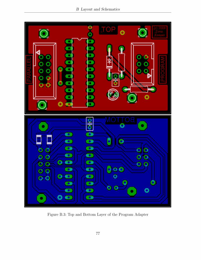
B Layout and Schematics
Figure B.3: Top and Bottom Layer of the Program Adapter
77
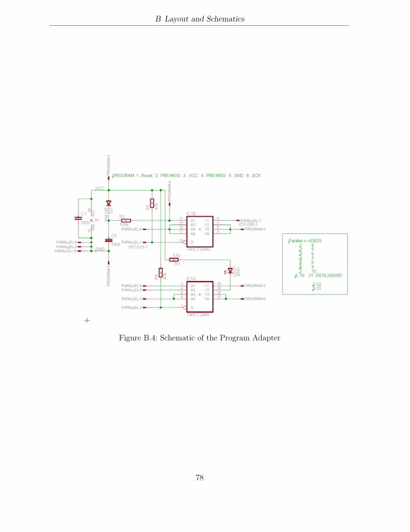
B Layout and Schematics
Figure B.4: Schematic of the Program Adapter
78

B Layout and Schematics
Figure B.5: Layout of the Reader, Version 2
79

B Layout and Schematics
Figure B.6: Top and Bottom Layer of the Reader, Version 2
80

B Layout and Schematics
Figure B.7: Schematic of the Reader, Version 2
81
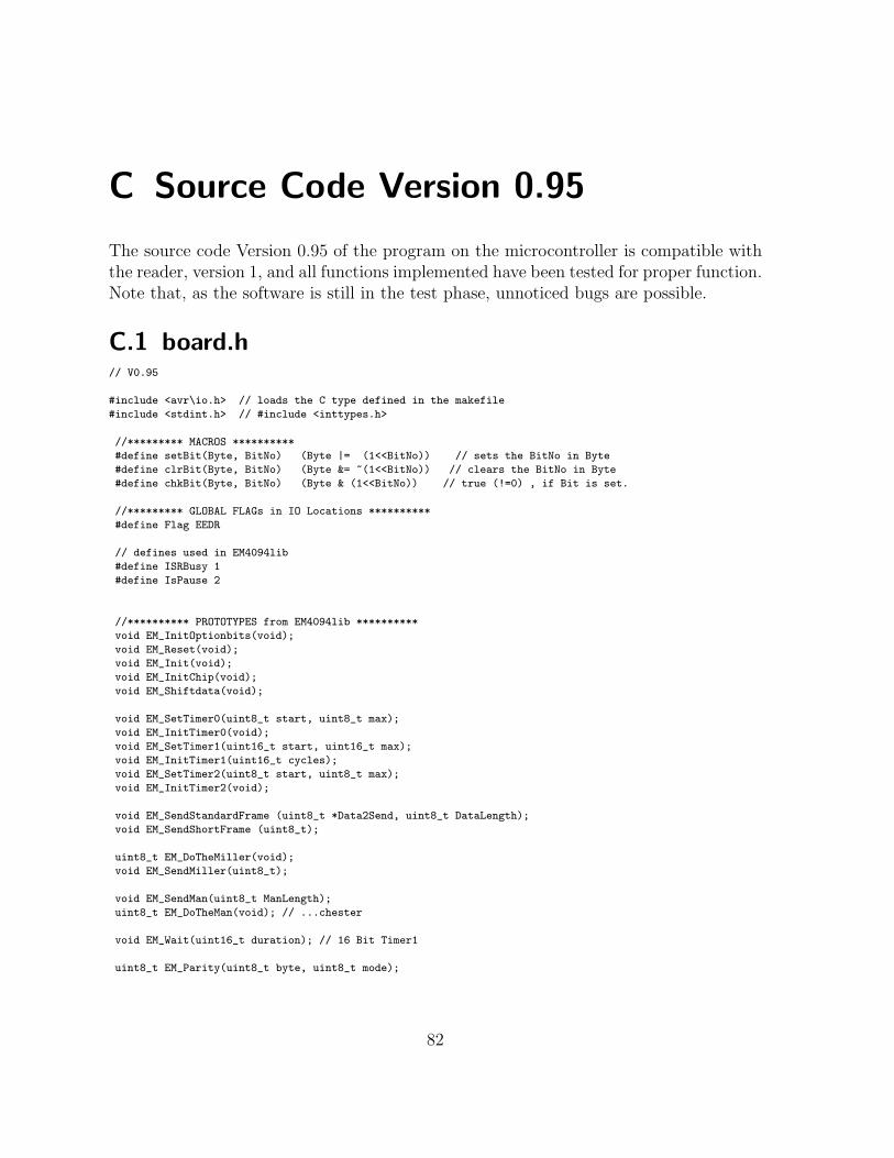
C Source Code Version 0.95
The source code Version 0.95 of the program on the microcontroller is compatible withthe reader, version 1, and all functions implemented have been tested for proper function.Note that, as the software is still in the test phase, unnoticed bugs are possible.
C.1 board.h// V0.95
#include <avr\io.h> // loads the C type defined in the makefile
#include <stdint.h> // #include <inttypes.h>
//********* MACROS **********
#define setBit(Byte, BitNo) (Byte |= (1<<BitNo)) // sets the BitNo in Byte
#define clrBit(Byte, BitNo) (Byte &= ~(1<<BitNo)) // clears the BitNo in Byte
#define chkBit(Byte, BitNo) (Byte & (1<<BitNo)) // true (!=0) , if Bit is set.
//********* GLOBAL FLAGs in IO Locations **********
#define Flag EEDR
// defines used in EM4094lib
#define ISRBusy 1
#define IsPause 2
//********** PROTOTYPES from EM4094lib **********
void EM_InitOptionbits(void);
void EM_Reset(void);
void EM_Init(void);
void EM_InitChip(void);
void EM_Shiftdata(void);
void EM_SetTimer0(uint8_t start, uint8_t max);
void EM_InitTimer0(void);
void EM_SetTimer1(uint16_t start, uint16_t max);
void EM_InitTimer1(uint16_t cycles);
void EM_SetTimer2(uint8_t start, uint8_t max);
void EM_InitTimer2(void);
void EM_SendStandardFrame (uint8_t *Data2Send, uint8_t DataLength);
void EM_SendShortFrame (uint8_t);
uint8_t EM_DoTheMiller(void);
void EM_SendMiller(uint8_t);
void EM_SendMan(uint8_t ManLength);
uint8_t EM_DoTheMan(void); // ...chester
void EM_Wait(uint16_t duration); // 16 Bit Timer1
uint8_t EM_Parity(uint8_t byte, uint8_t mode);
82

C Source Code Version 0.95
//********** PROTOTYPES from etcetera **********
void ETC_InitLEDs(void);
void ETC_Init(void);
void ETC_InitUSART(uint16_t baud);
uint8_t ETC_CheckButton(void);
uint8_t ETC_ReceiveByte(void);
void ETC_TransmitByte (uint8_t data);
//********** PROTOTYPES from ftlib **********
void FT_Init(void);
void FT_Send(uint8_t *USBData, uint8_t length);
uint8_t FT_Receive(uint8_t *USBData);
void FT_InitChip(void);
//********** VARIABLES from etcetera **********
// obsolete flags to be optimised / put into "Flag"
extern volatile uint8_t GogoLED; // flag for RunLEDs - used in former version of em4094lib & test.
extern volatile uint8_t RXflag; // flag for USART Receive
extern volatile uint8_t TXflag; // flag for USART Transmit
extern volatile uint8_t TXdata; // Transmitted data
extern volatile uint8_t RXdata; // Received data
//********** VARIABLES from EM4094lib *********
extern uint8_t MillerArray[256];
extern uint8_t Frame2Send[256];
// note: extern DECLARES variables for use in other libraries, still they must be DEFINED elsewhere!!
C.2 em4094lib.c/***************************************************************************************
*
* Title: Library for EM Microelectronics EM4094 chip
*
* Author: Timo Kasper
*
* Date: 051224 (yymmdd)
*
* Version: 0.95
*
* Purpose: Control EM4094 Chip with Atmel Mega Microcontroller
*
* Software: avrgcc compiler
*
* Hardware: ATMega32 (can be other ATMegas) + EM4094 IC
*
*
*
* Demands: + library shall be adaptable to "any" pin assignment C<==>EM4094.
* + the chip’s possibilities shall be accessible via the library functions.
* + All functions of this library have a default value.
* (see comments of individual functions)
*
*
* Note: contents of this library are strictly confidental.
*
* (c) 2005 Timo Kasper
83

C Source Code Version 0.95
*
***************************************************************************************
*
* The Serial interface is used to control the EM4094 option bits setting.
*
* After reset, the DIN signal is shifted to the internal register on every rising edge in
* DCLK. During first 31 DCLK transitions the DIN data is read to the chip while during the
* 32nd transition the chip enters the normal mode.
*
* During normal mode:
* DIN is the modulation input (high DIN: low reader filed for ASK or no field for OOK).
* DCLK must be low in normal mode.
* DOUT and DOUT1 are data and clock outputs in normal mode.
*
* The EM4094 system selection bits (in the sequence send to chip) are:
* Bit 1 Power up flag
* Bit 2 Modulation index selection 0
* Bit 3 Modulation index selection 1
* Bit 4 Modulation index selection 2
* Bit 5 Short circuit protection enable
* Bit 6 Single or dual RF driver selection
* Bit 7 Dual driver in phase or phase Opposite
* Bit 8 Filter zero selection 1
* Bit 9 Filter zero selection 2
* Bit 10 Filter low pass selection 400kHz
* Bit 11 Receive gain selection 0 (LSB)
* Bit 12 Receiver gain selection 1
* Bit 13 Receiver gain selection 2 (MSB)
* Bit 14 AM PM input channel selection
* Bit 15 AGC on off selection
* Bit 16 AGC attack mode selection
* Bit 17 AGC decay mode selection
* Bit 18 AGC attack rate (lsb)
* Bit 19 AGC attack rate (msb)
* Bit 20 AGC decay wait (lsb)
* Bit 21 AGC decay wait (msb)
* Bit 22 Output selection direct sub-carrier or BPSK 848kHz
* Bit 23 BPSK automatic frequency adjust
* Bit 24 Output selection analog
* Bit 25 Hold delay after modulation selection
* Bit 26 Oscillator gain selection
* Bit 27 External oscillator
* Bit 28 -> 31 Test mode selection (all LOW for normal operation)
*
**************************************************************************************
* board’s pinout:
*
* C | USB
* -------------+--------------------
* PA0...PA7 <--> D0...D7
* PC5 RXF#
* PC4 TXE#
* PC6 RD#
* PC7 WR
*
* C | LEDs etc.
* -------------+--------------------
* PB4 --> Rot1, LowActive
* PD4 --> Rot2, LowActive
* PC3 --> Gelb, LowActive
* PD3 --> Grn, LowActive
* PC2 <-- Pushbutton, LowActive
*
84

C Source Code Version 0.95
* C | EM4094
* -------------+--------------------
* PD7 --> DCLK
* PD6,PD2 <-- DOUT
* PB2 <-- DOUT1
* PB0 <-- DOUT1 / 16 (!)
* PD5 --> DIN
* PB3 --> DIN Pulse
* (note: JP2 ON --> DIN Pulse ACTIVE --> PD5 has to be set "TriState"!!)
* PB1 --> ENABLE
*
* C | Serial
* -------------+--------------------
* PD1 (TXD) --> MAX232 T1IN
* PD0 (RXD) <-- MAX232 R1OUT
*
* PC1 (SDA) (<)--> 2WireInterface Pin1 SDA
* PC0 (SCK) <--(>) 2WireInterface Pin2 SCK
*
**************************************************************************************/
// in board.h, extern variables etc. (everything that is used by all 3 libraries) are declared.
//********** INCLUDES **********
#include <stdint.h> // #include <inttypes.h>
#include <avr\io.h> // loads C type defined in makefile
#include <avr\delay.h>
#include <avr\signal.h> // necessary for ISRs
#include <avr\interrupt.h> // necessary for sei() / cli()
#include "board.h"
// ********** DEFINES **********
#define EOFrame 0xFF
#define MillerValue 63 // for setting of timer 0
#define WaitValue 2300
#define EM_SHDEL 1 // Shift delay (used during shifting serial data)
#define EM_EN_PORT PORTB // Enable Port
#define EM_EN_PIN PINB // Enable Pin
#define EM_EN_DDR DDRB // Enable DDR
#define EM_EN 1 // Enable Bit
#define EM_DIN_PORT PORTD // DIN Port
#define EM_DIN_PIN PIND // DIN Pin
#define EM_DIN_DDR DDRD // DIN DDR
#define EM_DIN 5 // DIN Bit
#define EM_DIN_PULSE_PORT PORTB // DIN_PULSE Port
#define EM_DIN_PULSE_PIN PINB // DIN_PULSE Pin
#define EM_DIN_PULSE_DDR DDRB // DIN_PULSE DDR
#define EM_DIN_PULSE 3 // DIN_PULSE Bit
#define EM_DCLK_PORT PORTD // DCLK Port
#define EM_DCLK_PIN PIND // DCLK Pin
#define EM_DCLK_DDR DDRD // DCLK DDR
85

C Source Code Version 0.95
#define EM_DCLK 7 // DCLK Bit
// DOUT is connected to 2 pins: PD2, PD6 --> DOUT_1, DOUT_2 (!= DOUT1)
#define EM_DOUT_1_PORT PORTD // DOUT Port
#define EM_DOUT_1_PIN PIND // DOUT Pin
#define EM_DOUT_1_DDR DDRD // DOUT DDR
#define EM_DOUT_1 2 // DOUT_1 Bit
#define EM_DOUT_2_PORT PORTD // DOUT Port
#define EM_DOUT_2_PIN PIND // DOUT Pin
#define EM_DOUT_2_DDR DDRD // DOUT DDR
#define EM_DOUT_2 6 // DOUT_2 Bit
#define EM_DOUT1_PORT PORTB // DOUT1 Port (don’t mix up with DOUT_1 !)
#define EM_DOUT1_PIN PINB // DOUT1 Pin
#define EM_DOUT1_DDR DDRB // DOUT1 DDR
#define EM_DOUT1 2 // DOUT1 Bit
#define EM_DOUT1_16_PORT PORTB // DOUT1/16 Port
#define EM_DOUT1_16_PIN PINB // DOUT1/16 Pin
#define EM_DOUT1_16_DDR DDRB // DOUT1/16 DDR
#define EM_DOUT1_16 0 // DOUT1/16 Bit
//For Manchester Code Output
#define EM_MAN_OUT_PORT PORTC
#define EM_MAN_OUT_PIN PINC
#define EM_MAN_OUT_DDR DDRC
#define EM_MAN_OUT 0
//********* MACROS **********
//(setBit/clrBit/chkBit(Byte, BitNo) defined in board.h)
//(only needed for Output ports/pins, NOT for INPUT (e.g. DOUT1,DOUT)
#define EN_HIGH setBit (EM_EN_PORT, EM_EN)
#define EN_LOW clrBit (EM_EN_PORT, EM_EN)
#define DIN_HIGH setBit (EM_DIN_PORT, EM_DIN)
#define DIN_LOW clrBit (EM_DIN_PORT, EM_DIN)
#define DCLK_HIGH setBit (EM_DCLK_PORT, EM_DCLK)
#define DCLK_LOW clrBit (EM_DCLK_PORT, EM_DCLK)
#define MAN_OUT_LOW clrBit (EM_MAN_OUT_PORT, EM_MAN_OUT)
#define MAN_OUT_HIGH setBit (EM_MAN_OUT_PORT, EM_MAN_OUT)
//pulsed DIN:
#define DIN_P_HIGH setBit (EM_DIN_PULSE_PORT, EM_DIN_PULSE)
#define DIN_P_LOW clrBit (EM_DIN_PULSE_PORT, EM_DIN_PULSE)
//Timers: 0. Init Timer Values ,1. INT on, 2. Timer start ; Do S.TH. ; 3. INT off 4. Timer stop.
//T0
#define INT_T0_ON setBit (TIMSK,OCIE0) // ENable Timer0 Interrupt; (TIMSK, Bit OCIE0=1)
#define INT_T0_OFF clrBit (TIMSK,OCIE0) // DISable Timer interrupt; (TIMSK, Bit OCIE0=0)
#define T0_START setBit (TCCR0,CS00) // No Prescaler, TIMER0 RUN
#define T0_STOP clrBit(TCCR0,CS00);clrBit(TCCR0,CS01);clrBit(TCCR0,CS02) // Timer0 STOP
//T1
#define INT_T1_ON setBit (TIMSK,OCIE1A) // ENable Timer1 Output Compare A Interrupt; (TIMSK, Bit OCIE0=1)
#define INT_T1_OFF clrBit (TIMSK,OCIE1A) // DISable Timer1 Output Compare A interrupt; (TIMSK, Bit OCIE0=0)
86

C Source Code Version 0.95
#define T1_START setBit (TCCR1B,CS10) // No Prescaler, TIMER1 RUN
#define T1_STOP clrBit(TCCR1B,CS10);clrBit(TCCR1B,CS11);clrBit(TCCR1B,CS12) // Timer0 STOP
//T2
#define INT_T2_ON setBit (TIMSK,OCIE2) // ENable Timer2 Interrupt; (TIMSK, Bit OCIE2=1)
#define INT_T2_OFF clrBit (TIMSK,OCIE2) // DISable Timer2 interrupt; (TIMSK, Bit OCIE2=0)
#define T2_START setBit (TCCR2,CS20) // No Prescaler, TIMER2 RUN
#define T2_STOP clrBit(TCCR2,CS20);clrBit(TCCR2,CS21);clrBit(TCCR2,CS22) // Timer2 STOP
/* if short delay is needed (without using interrupts):
void _delay_ms ( double __ms )
The maximal possible delay is 262.14 ms / F_CPU in MHz.
void _delay_us ( double __us )
The maximal possible delay is 768 us / F_CPU in MHz.
note: (F_CPU has to be set correctly ion the makefile)
*/
// Note (if needed) NAKED_ISR --> NO registers saved at beginning,
// NO RETI at the END!! (Do manually!)
#define NAKED_ISR(vector) \
void vector (void) __attribute__ ((naked)); \
void vector (void)
//********** VARIABLE DEFINITIONS **********
// DO THE ARRAYS HAVE TO BE INITIALIZED ?
uint8_t Frame2Send[256]; // ends with EOFrame (DEFINED above)
// Frame2Send data format: 0=SOC, 1=One, 2=Zero, 3=EOC2 (EOC1 equals "0")
// 1 Byte IS EQUAL TO ONE HALF BIT :-(
uint8_t MillerArray[256];
uint8_t ManArray[256];
// Bit field
volatile struct
{
// UNSIGNED char ensures, that no bits are used as a +/- flag.
volatile uint8_t Bit1 : 1; // Power up flag
volatile uint8_t Bit2 : 1; // Modulation index selection 0
volatile uint8_t Bit3 : 1; // Modulation index selection 1
volatile uint8_t Bit4 : 1; // Modulation index selection 2
volatile uint8_t Bit5 : 1; // Short circuit protection enable
volatile uint8_t Bit6 : 1; // Single or dual RF driver selection
volatile uint8_t Bit7 : 1; // Dual driver in phase or phase Opposite
volatile uint8_t Bit8 : 1; // Filter zero selection 1
volatile uint8_t Bit9 : 1; // Filter zero selection 2
volatile uint8_t Bit10 : 1; // Filter low pass selection 400kHz
volatile uint8_t Bit11 : 1; // Receive gain selection 0 (LSB)
volatile uint8_t Bit12 : 1; // Receiver gain selection 1
volatile uint8_t Bit13 : 1; // Receiver gain selection 2 (MSB)
volatile uint8_t Bit14 : 1; // AM PM input channel selection
volatile uint8_t Bit15 : 1; // AGC on off selection
volatile uint8_t Bit16 : 1; // AGC attack mode selection
volatile uint8_t Bit17 : 1; // AGC decay mode selection
volatile uint8_t Bit18 : 1; // AGC attack rate (lsb)
volatile uint8_t Bit19 : 1; // AGC attack rate (msb)
volatile uint8_t Bit20 : 1; // AGC decay wait (lsb)
volatile uint8_t Bit21 : 1; // AGC decay wait (msb)
87

C Source Code Version 0.95
volatile uint8_t Bit22 : 1; // Output selection direct sub-carrier or BPSK 848kHz
volatile uint8_t Bit23 : 1; // BPSK automatic frequency adjust
volatile uint8_t Bit24 : 1; // Output selection analog
volatile uint8_t Bit25 : 1; // Hold delay after modulation selection
volatile uint8_t Bit26 : 1; // Oscillator gain selection
volatile uint8_t Bit27 : 1; // External oscillator
volatile uint8_t Bit28 : 1; // Test mode selection (all LOW for normal operation)
volatile uint8_t Bit29 : 1; // Test mode selection (all LOW for normal operation)
volatile uint8_t Bit30 : 1; // Test mode selection (all LOW for normal operation)
volatile uint8_t Bit31 : 1; // Test mode selection (all LOW for normal operation)
// only 4 Byte of memory used
//access with Option.Bit2=0 (e.g.)
} Option;
// *********************************** ISRs **********************************
// keep ISRs short, eventually use global flags
SIGNAL (SIG_OUTPUT_COMPARE0) //from iom32.h, BIG LETTERS!!
{
// 8 Bit Timer
// Purpose: Output of "modified miller" coded data
// 1 Byte of MillerArray contains 1 Nibble Data (4 Bit Periods)
// Count DOWN the Current Bits and UP the Bytes to keep order...
if (chkBit(Flag,IsPause)) // if Current "HalfBit" == 1
{ // Send Pause
DIN_P_HIGH;
DIN_P_LOW;
}
clrBit(Flag,ISRBusy);
}
SIGNAL (SIG_OUTPUT_COMPARE1A)
{
// 16 Bit Timer
// Purpose: WAIT (i.e. just clear flag) for a period between 75 ns and 4,8 ms with a resolution of 75 ns
// e.g. 170 us is approx. 2305 clock cycles.
// Clear Flag
clrBit(Flag,ISRBusy);
}
SIGNAL (SIG_OUTPUT_COMPARE2)
{
// 8 Bit Timer
// Purpose: Output of Manchester coded data
if (chkBit(Flag,IsPause))
MAN_OUT_HIGH; // if IsPause=1 : Man.-Pin = HIGH
else
// asm volatile("nop\n\t"::);
MAN_OUT_LOW; // else (IsPause=0) Man.-Pin = LOW
clrBit(Flag,ISRBusy);
}
88

C Source Code Version 0.95
// ******************************** FUNCTIONS ********************************
void EM_InitOptionbits(void)
//sets "save" (working with existing board) default values for optionbits.
{
Option.Bit1=1; //Power Up
Option.Bit2=1; //OOK modulation
Option.Bit3=0;
Option.Bit4=0;
Option.Bit5=1; //short circuit protection ENabled
Option.Bit6=1; //use ant1 AND ant2
Option.Bit7=0; // * IN PHASE driving!!
Option.Bit8=0; // * 300KHz receiving filter
Option.Bit9=0;
Option.Bit10=0; //high cut off frequency
Option.Bit11=0; //nominal gain
Option.Bit12=0;
Option.Bit13=0;
Option.Bit14=0; //RF input 1 selected
Option.Bit15=1; // * AGC ACTIVATED
Option.Bit16=0; //AGC: attack always
Option.Bit17=0; //AGC: fast decay
Option.Bit18=0; //AGC: "fast attack"
Option.Bit19=0;
Option.Bit20=0; //AGC: decay wait 44us
Option.Bit21=0;
Option.Bit22=0; //BPSK decoder: off (direct subcarrier output)
Option.Bit23=0; //BPSK: no auto freq. adjust
Option.Bit24=1; // ** ENABLED BPSK: analogue output disabled
Option.Bit25=0; //BPSK: no hold delay (?)
Option.Bit26=1; // * oscillator: high gm
Option.Bit27=0; //oscillator: use internal (quartz) oscillator
Option.Bit28=0; //bits for test mode --> all LOW (for normal operation)
Option.Bit29=0;
Option.Bit30=0;
Option.Bit31=0;
}
void EM_InitChip(void)
// to be configured as INPUT: DOUT_1,2 (both ports) , DOUT1
// to be configured as OUTPUT: EN, DIN (*), DIN_PULSE, DCLK
// (*) if JP2 is plugged on --> DIN must TRISTATE while sending miller data!!
// device is enabled after InitChip
// note: ORDER of commands is important (for outputs):
// 1st: set PullUp (PORT)
// THEN set direction (DDR)
// otherwise "LOW-Peak" might occur ?!.
{
89
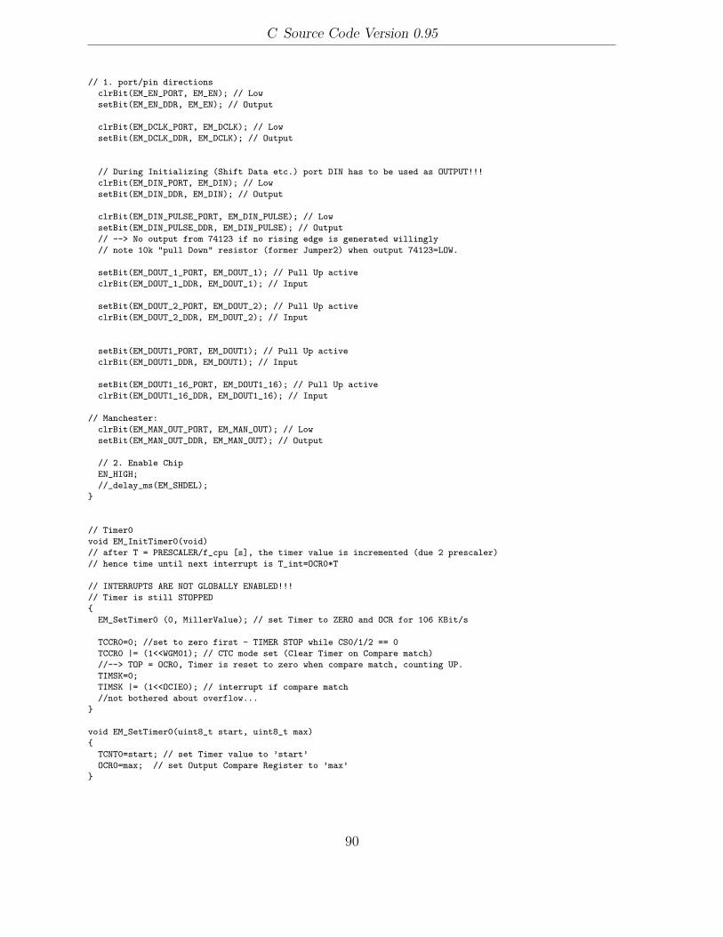
C Source Code Version 0.95
// 1. port/pin directions
clrBit(EM_EN_PORT, EM_EN); // Low
setBit(EM_EN_DDR, EM_EN); // Output
clrBit(EM_DCLK_PORT, EM_DCLK); // Low
setBit(EM_DCLK_DDR, EM_DCLK); // Output
// During Initializing (Shift Data etc.) port DIN has to be used as OUTPUT!!!
clrBit(EM_DIN_PORT, EM_DIN); // Low
setBit(EM_DIN_DDR, EM_DIN); // Output
clrBit(EM_DIN_PULSE_PORT, EM_DIN_PULSE); // Low
setBit(EM_DIN_PULSE_DDR, EM_DIN_PULSE); // Output
// --> No output from 74123 if no rising edge is generated willingly
// note 10k "pull Down" resistor (former Jumper2) when output 74123=LOW.
setBit(EM_DOUT_1_PORT, EM_DOUT_1); // Pull Up active
clrBit(EM_DOUT_1_DDR, EM_DOUT_1); // Input
setBit(EM_DOUT_2_PORT, EM_DOUT_2); // Pull Up active
clrBit(EM_DOUT_2_DDR, EM_DOUT_2); // Input
setBit(EM_DOUT1_PORT, EM_DOUT1); // Pull Up active
clrBit(EM_DOUT1_DDR, EM_DOUT1); // Input
setBit(EM_DOUT1_16_PORT, EM_DOUT1_16); // Pull Up active
clrBit(EM_DOUT1_16_DDR, EM_DOUT1_16); // Input
// Manchester:
clrBit(EM_MAN_OUT_PORT, EM_MAN_OUT); // Low
setBit(EM_MAN_OUT_DDR, EM_MAN_OUT); // Output
// 2. Enable Chip
EN_HIGH;
//_delay_ms(EM_SHDEL);
}
// Timer0
void EM_InitTimer0(void)
// after T = PRESCALER/f_cpu [s], the timer value is incremented (due 2 prescaler)
// hence time until next interrupt is T_int=OCR0*T
// INTERRUPTS ARE NOT GLOBALLY ENABLED!!!
// Timer is still STOPPED
{
EM_SetTimer0 (0, MillerValue); // set Timer to ZERO and OCR for 106 KBit/s
TCCR0=0; //set to zero first - TIMER STOP while CS0/1/2 == 0
TCCR0 |= (1<<WGM01); // CTC mode set (Clear Timer on Compare match)
//--> TOP = OCR0, Timer is reset to zero when compare match, counting UP.
TIMSK=0;
TIMSK |= (1<<OCIE0); // interrupt if compare match
//not bothered about overflow...
}
void EM_SetTimer0(uint8_t start, uint8_t max)
{
TCNT0=start; // set Timer value to ’start’
OCR0=max; // set Output Compare Register to ’max’
}
90
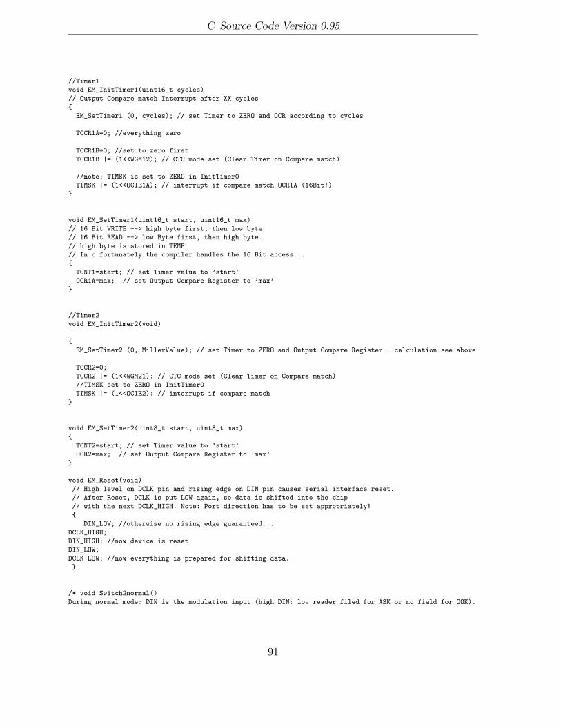
C Source Code Version 0.95
//Timer1
void EM_InitTimer1(uint16_t cycles)
// Output Compare match Interrupt after XX cycles
{
EM_SetTimer1 (0, cycles); // set Timer to ZERO and OCR according to cycles
TCCR1A=0; //everything zero
TCCR1B=0; //set to zero first
TCCR1B |= (1<<WGM12); // CTC mode set (Clear Timer on Compare match)
//note: TIMSK is set to ZERO in InitTimer0
TIMSK |= (1<<OCIE1A); // interrupt if compare match OCR1A (16Bit!)
}
void EM_SetTimer1(uint16_t start, uint16_t max)
// 16 Bit WRITE --> high byte first, then low byte
// 16 Bit READ --> low Byte first, then high byte.
// high byte is stored in TEMP
// In c fortunately the compiler handles the 16 Bit access...
{
TCNT1=start; // set Timer value to ’start’
OCR1A=max; // set Output Compare Register to ’max’
}
//Timer2
void EM_InitTimer2(void)
{
EM_SetTimer2 (0, MillerValue); // set Timer to ZERO and Output Compare Register - calculation see above
TCCR2=0;
TCCR2 |= (1<<WGM21); // CTC mode set (Clear Timer on Compare match)
//TIMSK set to ZERO in InitTimer0
TIMSK |= (1<<OCIE2); // interrupt if compare match
}
void EM_SetTimer2(uint8_t start, uint8_t max)
{
TCNT2=start; // set Timer value to ’start’
OCR2=max; // set Output Compare Register to ’max’
}
void EM_Reset(void)
// High level on DCLK pin and rising edge on DIN pin causes serial interface reset.
// After Reset, DCLK is put LOW again, so data is shifted into the chip
// with the next DCLK_HIGH. Note: Port direction has to be set appropriately!
{
DIN_LOW; //otherwise no rising edge guaranteed...
DCLK_HIGH;
DIN_HIGH; //now device is reset
DIN_LOW;
DCLK_LOW; //now everything is prepared for shifting data.
}
/* void Switch2normal()
During normal mode: DIN is the modulation input (high DIN: low reader filed for ASK or no field for OOK).
91

C Source Code Version 0.95
DCLK must be low in normal mode.
DOUT and DOUT1 are data and clock outputs in normal mode.*/
void EM_Shiftdata(void)
// shifts the previously set option bits to the device
// premises: serial Reset is performed AND DCLK is LOW.
// AFTER this function, EM4094 chip is in NORMAL MODE! (DCLK=LOW,DIN=LOW)
// sequence for 1 bit:
// 1. put (next) option bit to DIN-Pin
// 2. wait EM_SHDEL ms
// 3. DCLK (LOW)-->HIGH (--> data is in shift register)
// 4. wait EM_SHDEL ms
// 5. DCLK (HIGH)-->LOW
// goto 1.
{
char count;
for (count=1;count <= 31;count++)
{
switch(count)
{
// set corresponding option bit
case 1: if (Option.Bit1) DIN_HIGH; else DIN_LOW; break;
case 2: if (Option.Bit2) DIN_HIGH; else DIN_LOW; break;
case 3: if (Option.Bit3) DIN_HIGH; else DIN_LOW; break;
case 4: if (Option.Bit4) DIN_HIGH; else DIN_LOW; break;
case 5: if (Option.Bit5) DIN_HIGH; else DIN_LOW; break;
case 6: if (Option.Bit6) DIN_HIGH; else DIN_LOW; break;
case 7: if (Option.Bit7) DIN_HIGH; else DIN_LOW; break;
case 8: if (Option.Bit8) DIN_HIGH; else DIN_LOW; break;
case 9: if (Option.Bit9) DIN_HIGH; else DIN_LOW; break;
case 10: if (Option.Bit10) DIN_HIGH; else DIN_LOW; break;
case 11: if (Option.Bit11) DIN_HIGH; else DIN_LOW; break;
case 12: if (Option.Bit12) DIN_HIGH; else DIN_LOW; break;
case 13: if (Option.Bit13) DIN_HIGH; else DIN_LOW; break;
case 14: if (Option.Bit14) DIN_HIGH; else DIN_LOW; break;
case 15: if (Option.Bit15) DIN_HIGH; else DIN_LOW; break;
case 16: if (Option.Bit16) DIN_HIGH; else DIN_LOW; break;
case 17: if (Option.Bit17) DIN_HIGH; else DIN_LOW; break;
case 18: if (Option.Bit18) DIN_HIGH; else DIN_LOW; break;
case 19: if (Option.Bit19) DIN_HIGH; else DIN_LOW; break;
case 20: if (Option.Bit20) DIN_HIGH; else DIN_LOW; break;
case 21: if (Option.Bit21) DIN_HIGH; else DIN_LOW; break;
case 22: if (Option.Bit22) DIN_HIGH; else DIN_LOW; break;
case 23: if (Option.Bit23) DIN_HIGH; else DIN_LOW; break;
case 24: if (Option.Bit24) DIN_HIGH; else DIN_LOW; break;
case 25: if (Option.Bit25) DIN_HIGH; else DIN_LOW; break;
case 26: if (Option.Bit26) DIN_HIGH; else DIN_LOW; break;
case 27: if (Option.Bit27) DIN_HIGH; else DIN_LOW; break;
case 28: if (Option.Bit28) DIN_HIGH; else DIN_LOW; break;
case 29: if (Option.Bit29) DIN_HIGH; else DIN_LOW; break;
case 30: if (Option.Bit30) DIN_HIGH; else DIN_LOW; break;
case 31: if (Option.Bit31) DIN_HIGH; else DIN_LOW; break;
}
// shift once
DCLK_HIGH;
DCLK_LOW;
} //end for (--> next bit)
DIN_LOW; // appears reasonable ;-)
92

C Source Code Version 0.95
// shift one more time to enter normal mode !
DCLK_HIGH;
DCLK_LOW;
}
void EM_Init(void)
{
// set variables (struct)
EM_InitOptionbits();
// set Port directions and Enable device
EM_InitChip();
// enable Device is included in InitChip
// reset serial interface of device
EM_Reset();
// shift (previously set) data to the device.
EM_Shiftdata();
// after shiftdata: wait for DOUT=HIGH? - see below
// for test purposes: delay instead
_delay_ms (1);
EM_InitTimer0(); // Initialise the timer used to control MILLER communication
EM_InitTimer1(WaitValue); // Initialise the "wait" timer
EM_InitTimer2(); // Initialise the timer used to control MANCHESTER communication
// IF power Down mode (bit 1 L-->H or EN L-->H) --> startup procedure of chip
// --> DOUT pin = high for 100us, then chip goes 2 normal mode.
// IF short circuit detected between startup --> DOUT remains LOW, DOUT1 goes HIGH.
// note: normal mode --> dout1=clock output 13.56MHz
// and high DIN = No field (in OOK) --> set DIN to low for tests.
// --> eventually take this into account by
// 1. make sure, that power down mode. (e.g. EN=LOW)
// 2. Init and WAIT for DOUT rising edge for say 1-2 ms.
// 3. if not, detect error (maybe even look for DOUT1=HIGH?) --> red LED on.
}
void EM_SendShortFrame (uint8_t Byte2Send) // only 7 Bit, MSB will be ignored.
// Short frame: [SOC b1...b7 EOC] (LSB first)
// routine puts the above pattern into (Frame2Send) array
// 0=SOC, 1=One, 2=Zero, 3=EOC2 (EOC1 equals "0")
{
uint8_t FramePointer=0;
Frame2Send[FramePointer++]=0; // SOC
for (uint8_t CurrentBit=0;CurrentBit<=6;CurrentBit++){
if (Byte2Send&(1<<CurrentBit)) { // Bit "CurrentBit" is SET
// ********** SEND ONE **********
Frame2Send[FramePointer++]=1;
}
else { // Bit "CurrentBit" is NOT SET
// ********** SEND ZERO **********
93

C Source Code Version 0.95
Frame2Send[FramePointer++]=2;
}
} // END FOR
Frame2Send[FramePointer++]=2; // EOC part 1 = "Zero"
Frame2Send[FramePointer++]=3; // EOC part 2
Frame2Send[FramePointer]=EOFrame;
}
//******************************************************************************************
void EM_SendStandardFrame (uint8_t *Data2Send, uint8_t DataLength)
// DataLength=No. of Bytes in Data2Send Array
// limited to max. 28 data Bytes (array size!)
// Standard frame: [SOC b1...b8 P b1...b8 P ...(n times)... EOC] (LSB first, P=odd parity bit)
// routine puts the above pattern into (Frame2Send) array FIRST BYTE of Data2Send IS SENT FIRST!!
// 0=SOC, 1=One, 2=Zero, 3=EOC
{
uint8_t DataPointer=0;
uint8_t FramePointer=0;
uint8_t tmp;
Frame2Send[FramePointer++]=0; // SOC
do
{
for (uint8_t CurrentBit=0;CurrentBit<=7;CurrentBit++){
// Bit2Send = Byte2Send & (1<<CurrentBit); --> LSB sent first if CurrentBit counted UP
if (Data2Send[DataPointer]&(1<<CurrentBit)) { // Bit "CurrentBit" is SET
// ********** SEND ONE **********
Frame2Send[FramePointer++]=1;
}
else { // Bit "CurrentBit" is NOT SET
// ********** SEND ZERO **********
Frame2Send[FramePointer++]=2;
}
} // END FOR
// Add (Odd) Parity Bit
// Careful: if Parity returns Zero, a "2" wants to be put in the frame array !
tmp=EM_Parity(Data2Send[DataPointer],1);
if (tmp==0) Frame2Send[FramePointer++]=(tmp+2); // Zero is "2" in frame array
else Frame2Send[FramePointer++]=tmp;
} while (++DataPointer < DataLength); // DataPointer must never become == DataLength in do..while loop
Frame2Send[FramePointer++]=2; // EOC part 1 = "Zero" (for miller compability)
Frame2Send[FramePointer++]=3; // EOC part 2 = "Real EOC indicator"
Frame2Send[FramePointer]=EOFrame;
}
uint8_t EM_Parity(uint8_t byte, uint8_t mode)
// returns Parity bit for odd(mode=1) or even(mode=0) parity
// !! CAUTION: for Zero, a 0 is returned, but in Frame2Send Zero equals 2 !!
{
byte ^= (byte >> 4);
byte ^= (byte >> 2);
byte ^= (byte >> 1);
94
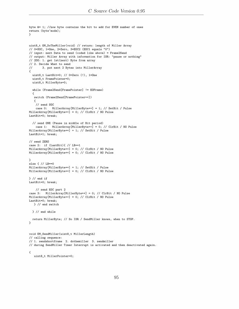
C Source Code Version 0.95
byte &= 1; //now byte contains the bit to add for EVEN number of ones
return (byte^mode);
}
uint8_t EM_DoTheMiller(void) // return: length of Miller Array
// 0=SOC, 1=One, 2=Zero, 3=EOC2 (EOC1 equals "0")
// input: next Data to send (coded like above) = Frame2Send
// output: Miller Array with information for ISR: "pause or nothing"
// 2DO: 1. get 1st(next) Byte from array
// 2. Decide What to send
// 3. put next 2 Bytes into MillerArray
{
uint8_t LastBit=0; // 0=Zero (!), 1=One
uint8_t FramePointer=0;
uint8_t MillerByte=0;
while (Frame2Send[FramePointer] != EOFrame)
{
switch (Frame2Send[FramePointer++])
{
// send SOC
case 0: MillerArray[MillerByte++] = 1; // SetBit / Pulse
MillerArray[MillerByte++] = 0; // ClrBit / NO Pulse
LastBit=0; break;
// send ONE (Pause in middle of Bit period)
case 1: MillerArray[MillerByte++] = 0; // ClrBit / NO Pulse
MillerArray[MillerByte++] = 1; // SetBit / Pulse
LastBit=1; break;
// send ZERO
case 2: if (LastBit){ // LB==1
MillerArray[MillerByte++] = 0; // ClrBit / NO Pulse
MillerArray[MillerByte++] = 0; // ClrBit / NO Pulse
}
else { // LB==0
MillerArray[MillerByte++] = 1; // SetBit / Pulse
MillerArray[MillerByte++] = 0; // ClrBit / NO Pulse
} // end if
LastBit=0; break;
// send EOC part 2
case 3: MillerArray[MillerByte++] = 0; // ClrBit / NO Pulse
MillerArray[MillerByte++] = 0; // ClrBit / NO Pulse
LastBit=0; break;
} // end switch
} // end while
return MillerByte; // So ISR / SendMiller knows, when to STOP.
}
void EM_SendMiller(uint8_t MillerLength)
// calling sequence:
// 1. sendshortframe 2. dothemiller 3. sendmiller
// during SendMiller Timer Interrupt is activated and then deactivated again.
{
uint8_t MillerPointer=0;
95

C Source Code Version 0.95
EM_SetTimer0 (0, MillerValue); // (Re)set Timer0 and Output Compare Register
setBit(Flag,ISRBusy);
// hier "schlimme" nderung (zeitmssig)?
// IsPause=MillerArray[MillerPointer++]; // Prefetch 1st bit value for ISR
// if (MillerArray[MillerPointer++]){setBit(Flag,IsPause);}
// else {clrBit(Flag,IsPause);}
INT_T0_ON;
T0_START;
do {
if (MillerArray[MillerPointer++]){setBit(Flag,IsPause);}
else {clrBit(Flag,IsPause);}
setBit (Flag,ISRBusy);
do {} while (chkBit(Flag,ISRBusy)) ; // react to current Half Bit Period
// IsPause=MillerArray[MillerPointer++]; // Prefetch NEXT bit value for ISR
} while (--MillerLength);
INT_T0_OFF;
T0_STOP;
}
uint8_t EM_DoTheMan(void) // ...chester. return: length of ManArray
// 0=SOC, 1=One, 2=Zero, 3=EOC
// input: next Data to send (coded like above) = Frame2Send
// output: Manchester Array with information for ISR: HIGH or LOW Half Bit Period
// note: modulation with f/16 is done externally with a binary counter.
{
uint8_t FramePointer=0;
uint8_t ManByte=0;
while (Frame2Send[FramePointer] != EOFrame)
{
switch (Frame2Send[FramePointer++])
{
// send SOC (= Logic ONE)
case 0: ManArray[ManByte++] = 1;
ManArray[ManByte++] = 0;
break;
// send ONE
case 1: ManArray[ManByte++] = 1;
ManArray[ManByte++] = 0;
break;
// send ZERO / EOC ?
// note: Miller compability: case 3(EOC) is already included in case 2 !
case 2: if (Frame2Send[FramePointer]==3) { // if next data to be sent = EOC
ManArray[ManByte++] = 0; // ignore this ZERO and put EOC instead
ManArray[ManByte++] = 0;
}
else { // this IS a Zero...
ManArray[ManByte++] = 0; // ...so let’s send it.
ManArray[ManByte++] = 1;
}
break;
} // end switch
96
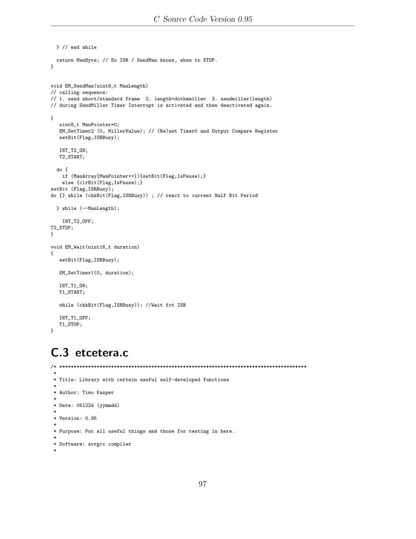
C Source Code Version 0.95
} // end while
return ManByte; // So ISR / SendMan knows, when to STOP.
}
void EM_SendMan(uint8_t ManLength)
// calling sequence:
// 1. send short/standard frame 2. length=dothemiller 3. sendmiller(length)
// during SendMiller Timer Interrupt is activated and then deactivated again.
{
uint8_t ManPointer=0;
EM_SetTimer2 (0, MillerValue); // (Re)set Timer0 and Output Compare Register
setBit(Flag,ISRBusy);
INT_T2_ON;
T2_START;
do {
if (ManArray[ManPointer++]){setBit(Flag,IsPause);}
else {clrBit(Flag,IsPause);}
setBit (Flag,ISRBusy);
do {} while (chkBit(Flag,ISRBusy)) ; // react to current Half Bit Period
} while (--ManLength);
INT_T2_OFF;
T2_STOP;
}
void EM_Wait(uint16_t duration)
{
setBit(Flag,ISRBusy);
EM_SetTimer1(0, duration);
INT_T1_ON;
T1_START;
while (chkBit(Flag,ISRBusy)); //Wait fot ISR
INT_T1_OFF;
T1_STOP;
}
C.3 etcetera.c/* **************************************************************************************
*
* Title: Library with certain useful self-developed functions
*
* Author: Timo Kasper
*
* Date: 051224 (yymmdd)
*
* Version: 0.95
*
* Purpose: Put all useful things and those for testing in here.
*
* Software: avrgcc compiler
*
97

C Source Code Version 0.95
* Hardware: ATMega32 (can be other ATMegas)
*
*
* (c) 2005 Timo Kasper
*
* *************************************************************************************/
// function prototypes put into board.h for convenience
//********** INCLUDES **********
#include <stdint.h> // #include <inttypes.h>
#include <avr\io.h> // loads C type defined in makefile
#include <avr\signal.h> // necessary for ISRs
#include <avr\interrupt.h> //necessary for sei() / cli()
#include "board.h"
// ********** DEFINES **********
#define RED1_PORT PORTB // Port
#define RED1_PIN PINB // Pin
#define RED1_DDR DDRB // DDR
#define RED1 4 // Bit
#define RED2_PORT PORTD // Port
#define RED2_PIN PIND // Pin
#define RED2_DDR DDRD // DDR
#define RED2 4 // Bit
#define GREEN_PORT PORTD // Port
#define GREEN_PIN PIND // Pin
#define GREEN_DDR DDRD // DDR
#define GREEN 3 // Bit
#define YELLOW_PORT PORTC // Port
#define YELLOW_PIN PINC // Pin
#define YELLOW_DDR DDRC // DDR
#define YELLOW 3 // Bit
#define BUTTON_PORT PORTC // Port
#define BUTTON_PIN PINC // Pin
#define BUTTON_DDR DDRC // DDR
#define BUTTON 2 // Bit
// ********** VARIABLE DEFINITIONS **********
// !!all variables read by ISR and main routine have to be volatile!!
// (otherwise data might be put into registers and overwritten before ISR reads them)
// (makes the access to these variables slower-not allowed to put in registers!!)
volatile uint8_t LEDstate, dir;
/* not needed here but might be useful elsewhere:
typedef union
{
uint16_t i16;
struct
{
uint8_t i8l;
uint8_t i8h;
};
98

C Source Code Version 0.95
} convert16to8;
convert16to8 baud;
*/
// ********** FUNCTIONS **********
void ETC_InitLEDs(void)
// inits Port directions etc.
{
// to be optimised: write ONE BYTE instead of multiple bits.
clrBit(RED1_PORT, RED1); // High
setBit(RED1_DDR, RED1); // Output
clrBit(RED2_PORT, RED2); // High
setBit(RED2_DDR, RED2); // Output
clrBit(YELLOW_PORT, YELLOW); // High
setBit(YELLOW_DDR, YELLOW); // Output
clrBit(GREEN_PORT, GREEN); // Low
setBit(GREEN_DDR, GREEN); // Output
setBit(BUTTON_PORT, BUTTON); // Pull Up active
clrBit(BUTTON_DDR, BUTTON); // Input / Tristate
LEDstate=0; //initialize running light
dir=1; // 1 is count UP 0 is count DOWN.
}
uint8_t ETC_CheckButton(void)
{ // TRUE if pressed
uint8_t Button;
Button = chkBit(BUTTON_PIN,BUTTON);
return (!Button);
}
void ETC_Init(void)
// Inits LEDs, USART
{
ETC_InitLEDs();
ETC_InitUSART(ubrr_setting); // different values have to be tested...
}
// OBSOLETE:
// Baud rates: Refer to table p.164 ATMega32 datasheet for setting of UBRR
// and aberration from exact value
// For normal (not 2x) mode: UBRR = fosc/(16*baudrate) - 1
// possible: #define baudrate 115200
// #define ubrr_setting f_cpu / (16 * baudrate ) - 1
// but note: Truncation--> not properly rounded int.
// #define ubrr_setting 6 // 6 is approx.115200 bps @ 13.56MHz (soll 6,35)
#define ubrr_setting 14 // 14 is approx. 57600 bps @ 13.56MHz (soll 13,71)
99

C Source Code Version 0.95
// #define ubrr_setting 87 // 87 is approx. 9600 bps @ 13.56MHz
// #define ubrr_setting 705 // 705 is approx. 1200 bps @ 13.56MHz
//UART
#define INT_TX_ON setBit (UCSRB,UDRIE) // ENable TX Interrupt
#define INT_TX_OFF clrBit (UCSRB,UDRIE) // DISable TX Interrupt
#define INT_RX_ON setBit (UCSRB,RXCIE) // ENable RX Interrupt
#define INT_RX_OFF clrBit (UCSRB,RXCIE) // DISable RX Interrupt
#define TX_ON setBit (UCSRB,TXEN) // ENable TX
#define TX_OFF clrBit (UCSRB,TXEN) // DISable TX
#define RX_ON setBit (UCSRB,RXEN) // ENable RX
#define RX_OFF clrBit (UCSRB,RXEN) // DISable RX
volatile uint8_t GogoLED=0;
volatile uint8_t TXdata; // for TX ISR
volatile uint8_t RXdata; // for RX ISR
// *********************************** ISRs **********************************
// keep ISRs short, eventually use global flags
SIGNAL (SIG_USART_RECV) // received char ready to be picked up
// RXC flag is ("automatically") cleared when reading UDR
// (ONE if new data is available)
// for test purposes: just read out UDR into Rxdata and set flag
{
RXdata=UDR;
// clrBit(Flag,ISRBusy); not needed: look for RXC to become ZERO clrBit(Flag,ISRBusy);
}
SIGNAL (SIG_USART_DATA) // data buffer ready for new char to be transmitted
// UDRE flag is ("automatically") cleared when writing UDR
// --> chkBit(UCSRA,UDRE) is ZERO, when new data has been transferred to UDR
// AFTER RESET, UDRE FLAG IS AUTOMATICALLY SET
{
UDR=TXdata;
//not needed: look for UDRE to become ZERO clrBit(Flag,ISRBusy);
}
uint8_t ETC_ReceiveByte(void)
{
while (!chkBit(UCSRA,RXC));
return UDR;
}
void ETC_TransmitByte (uint8_t data)
{
while (!chkBit(UCSRA,UDRE));
UDR=data;
}
// ********** USART functions **********
// save time --> no parity.
100

C Source Code Version 0.95
void ETC_InitUSART(uint16_t baud)
// !Note: baud is NOT the baudrate, but the value to be written into UBRR!
// Here comes a lot of code with not really much effect...
// what about setting the port directions where the RX/TX pins are?
{
uint8_t tmp;
tmp=0; // just to be on the safe side
// No doubling of transmission speed --> better durability against unprecise baud rate generation
clrBit(tmp,U2X);
// No Multiprocessor mode
clrBit(tmp,MPCM);
UCSRA=tmp;
tmp=0; // just to be on the safe side
// DISable RX complete interrupt
// is already cleared clrBit(tmp,RXCIE);
// DISable USART data register empty interrupt
// is already cleared clrBit(tmp,UDRIE);
// DISable Receiver
// is already cleared clrBit(tmp,RXEN);
// Enable Transmitter
// is already cleared clrBit(tmp,TXEN);
// No 9th Bit needed
// clrBit(tmp,UCSZ2);
UCSRB=tmp;
tmp=0x80; // URSEL=MSB is One --> write to UCSRC
// Set Asynchronous mode
clrBit(tmp,UMSEL);
// No Parity
clrBit(tmp,UPM1);
clrBit(tmp,UPM0);
// 1 Stop Bit
clrBit(tmp,USBS);
// 8 Data Bits
setBit(tmp,UCSZ1);
setBit(tmp,UCSZ0);
UCSRC=tmp;
tmp=0; // URSEL=MSB is Zero --> write to UBRRH
tmp|=(0x0F & (uint8_t)(baud>>8)); // cast --> only lower bits are taken into account
// only write lower 4 Bits !!
UBRRH=tmp; // write higher 4 Bits of UBRR
UBRRL=(uint8_t)baud; // write lower Byte of UBRR
}
/*
void ETC_RunLEDs(void)
{
if (GogoLED)
{
uint8_t temp;
temp=SREG;
cli(); // deactivate interrupts - "disturbance free code" begins
GogoLED=0; // clear flag
// make LEDs running:
101

C Source Code Version 0.95
if (dir) LEDstate++; else LEDstate--;
PORTA = ((PORTA&0xF0) | (0x0F& ~(1<<LEDstate))); //LEDs ON if pin LOW.
// High nibble of port a remains unchanged (="Pull-upped"), low nibble=LEDs.
if ((LEDstate == 3)&& dir) dir=0;//count up AND "last LED" --> change direction.
if ((LEDstate == 0)&& ~dir) dir=1;//count down AND "first LED" --> change direction.
// if fourth LED=on then dir=down. if first LED=on then dir=up.
//"disturbance free code" ends
SREG=temp; // interrupt handling as it was before.
}
}
*/
C.4 ftlib.c/***************************************************************************************
*
* Title: Library for FT245RL chip
*
* Author: Timo Kasper
*
* Date: 051225 (yymmdd)
*
* Version: 0.95
*
* Purpose: Control FTDI FT245RL Chip with Atmel Mega Microcontroller
*
* Software: avrgcc compiler
*
* Hardware: ATMega32 (can be other ATMegas) + FT245RL IC
*
*
*
* Demands: + library shall be adaptable to "any" pin assignment C<==>FT245RL.
* + the chip’s possibilities shall be accessible via the library functions.
*
*
* Receive data at uC from PC:
* 1. wait while RXF# is H (L=data available)
* might not be necessary: >= 2 clockcycles between #RD H->L and RXF# L->H
* 2. #RD=H
* 3. #RD H --> L : Fetch current data from PC# into USB chip
* 4. #RD L : data at D[7...0] is valid until #RD=H
* 5. Fetch data into uC
* DURATION until next RD (step3) must be at least 50ms+80ms=130ms (>=2 clockcycles)
* proceed with 1 until all data is received, i.e. RFX# L for a long time
*
* Send data from uC to PC:
* 1. {wait while TXE# is H (L=chip ready for new data)}
* might not be necessary: >= 2 clockcycles between WR H->L and TXE# L->H
* 2. WR = H
* 3. Write valid data to D[7..0]
* 4. WR H --> L : Transfer data into USB chip
* proceed with 1 until all data sent.
*
*
**************************************************************************************
* pinout: (version 1)
*
* C | USB
102

C Source Code Version 0.95
* -------------+--------------------
* PA0...PA7 <--> D0...D7
* PC5 RXF#
* PC4 TXE#
* PC6 RD#
* PC7 WR
*
**************************************************************************************/
//********** INCLUDES **********
#include <stdint.h> // #include <inttypes.h>
#include <avr\io.h> // loads C type defined in makefile
#include <avr\delay.h>
#include <avr\signal.h> // necessary for ISRs
#include <avr\interrupt.h> // necessary for sei() / cli()
#include "board.h"
// in board.h, extern variables etc. (everything that is used by all libraries) are declared.
/* if short delay needed (without using interrupts):
void _delay_ms ( double __ms )
The maximal possible delay is 262.14 ms / F_CPU in MHz.
void _delay_us ( double __us )
The maximal possible delay is 768 us / F_CPU in MHz.
note: (F_CPU has to be set correctly)
*/
// ********** DEFINES **********
// value for RXtimer:
// x=14000 (--> wait approx. 1ms) should be OK.
#define RXTimer 14000
// working with Bytes --> No need for data pins to be bit adressable
#define FT_DATA_DDR DDRA // DDR
// !! note "non-standard" names
#define FT_DATA_PORT PORTA // Port for output
#define FT_DATA_PIN PINA // Pin for input
//The Rest
#define FT_TXE_PORT PORTC // Port
#define FT_TXE_PIN PINC // Pin
#define FT_TXE_DDR DDRC // DDR
#define FT_TXE 4 // Bit
#define FT_RXF_PORT PORTC // Port
#define FT_RXF_PIN PINC // Pin
#define FT_RXF_DDR DDRC // DDR
#define FT_RXF 5 // Bit
#define FT_RD_PORT PORTC // Port
#define FT_RD_PIN PINC // Pin
#define FT_RD_DDR DDRC // DDR
#define FT_RD 6 // Bit
#define FT_WR_PORT PORTC // Port
#define FT_WR_PIN PINC // Pin
103

C Source Code Version 0.95
#define FT_WR_DDR DDRC // DDR
#define FT_WR 7 // Bit
#define RD_HIGH setBit (FT_RD_PORT, FT_RD)
#define RD_LOW clrBit (FT_RD_PORT, FT_RD)
#define WR_HIGH setBit (FT_WR_PORT, FT_WR)
#define WR_LOW clrBit (FT_WR_PORT, FT_WR)
#define DATA_INPUT FT_DATA_PORT = 0xFF; FT_DATA_DDR = 0x00 // Active Pull Ups, Inputs
#define DATA_OUTPUT FT_DATA_PORT = 0x00; FT_DATA_DDR = 0xFF // Low, Outputs
//********* MACROS **********
//(setBit/clrBit/chkBit(Byte, BitNo) defined in board.h)
// faster - note that between 2 subsequent calls of the 2 macros below must be >=2 cycles
#define FT_WRITE(CurrentByte) WR_HIGH; FT_DATA_PORT=USBData[CurrentByte++]; WR_LOW
#define FT_READ(CurrentByte) RD_LOW; USBData[CurrentByte++]=FT_DATA_PIN; RD_HIGH
// might be needed somewhere: asm volatile("nop\n\t"::);
//********** VARIABLE DEFINITIONS **********
//(none)
// ******************************** FUNCTIONS ********************************
void FT_InitChip(void)
// to be configured as INPUT: TXE, RXF
// to be configured as OUTPUT: RD,WR
// Data Bits are initialized as INPUTS
{// port/pin directions
//INPUTS
setBit(FT_TXE_PORT, FT_TXE); // Pull Up active
clrBit(FT_TXE_DDR, FT_TXE); // Input
setBit(FT_RXF_PORT, FT_RXF); // Pull Up active
clrBit(FT_RXF_DDR, FT_RXF); // Input
DATA_INPUT; // all data bits pullup active,inputs
//OUTPUTS
clrBit(FT_RD_PORT, FT_RD); // Low
setBit(FT_RD_DDR, FT_RD); // Output
clrBit(FT_WR_PORT, FT_WR); // Low
setBit(FT_WR_DDR, FT_WR); // Output
}
uint8_t FT_Receive(uint8_t *USBData) // data received is put in USBData, lenght(bytes, max. 256!) is returned.
{
/* !NOTE RD has to be H before first call (and RXF=L)!
* ! TIMER1 has to be initialised (EM_InitTimer1(WaitValue)) before calling !
*
* Receive data at uC from PC:
* 1. #RD=H
* 2. #RD H --> L : Fetch current data from PC# into USB chip
* 3. #RD L : data at D[7...0] is valid until #RD=H
* DURATION until next RD (step2) must be at least 50ms+80ms=130ms (>=2 clockcycles)
* proceed with 1 until all data is received, i.e. RFX# L for a long time
*/
uint8_t CurrentByte=0;
104

C Source Code Version 0.95
DATA_INPUT; //set direction of corresponding uC pins to input
EM_SetTimer1(0, RXTimer); // set Timer1 Start and Timeout Value for "all data received"
// start RX timeout timer and interrupt here, so that ISRBusy=0 when time out.
// (Timer 1 ISR will clear flag)
setBit(Flag,ISRBusy);
// ISRBusy Flag will only be cleared (ny ISR) of timeout occurs
INT_T1_ON;
T1_START;
do
{
if (!chkBit(FT_RXF_PIN,FT_RXF)) // if data available
{
// Reset RX Timeout-Timer
TCNT1=0;
FT_READ(CurrentByte); // CurrentByte is automatically incremented
}
} while (chkBit(Flag,ISRBusy)); // while no RX timeout
INT_T1_OFF; //RX Timer not needed any more.
T1_STOP;
return CurrentByte; // equals number of received bytes in USBData array
}
void FT_Send(uint8_t *USBData, uint8_t length) // data to be sent (length < 256!) is in USBData
{
/* !NOTE WR has to be L before first call (and TXE = L)!
* 1. WR = H
* 2. Write valid data to D[7..0]
* 3. WR H --> L : Transfer data into USB chip
* proceed with 1 until all data sent.
*/
DATA_OUTPUT; //set direction of corresponding uC pins to output
while (chkBit(FT_TXE_PIN,FT_TXE)); // wait for TXF to become LOW
for (uint8_t CurrentByte=0;CurrentByte<length;) //note: CurrentByte is automatically incremented below!!
{
FT_WRITE(CurrentByte); // CurrentByte is automatically incremented
} // END FOR
}
void FT_Init(void)
{
// set Port directions
FT_InitChip();
// RD has to be set HIGH before first call of FT_Receive!
RD_HIGH;
// WR has to be set LOW before first call of FT_Send!
WR_LOW;
}
105

C Source Code Version 0.95
C.5 test.c// V 0.95
#include <avr\io.h>
#include <stdint.h>
#include "em4094lib.c"
#include <avr\delay.h>
#include "etcetera.c"
#include "board.h"
#include "ftlib.c"
#define onlyones 0xFF
#define onlyzeroes 0x00
#define onlymix 0xAA
#define onlymix2 0x55
#define pattern1 0x64
#define REQA 0x26
#define WUPA 0x52
// "0010011" to be sent --> (reverse,LSB sent first!) (0)1100100 = 0x64
//*********************************** main **********************************
int main (void)
{
uint8_t ML_tmp=0;
uint16_t tmp=0;
uint16_t delay=2020;
uint8_t rcv_length=0;
uint8_t ATQA[2]={0x04, 0x00}; // "Real Tag"’s answer to REQA
// uint8_t USBTest[5]={0x41, 0x42, 0x43, 13,10}; // ASCII "A" and "B",CR,LF
const char* Text ="Current " "state: " "\n\r";
uint8_t USBHello[]={10,13,’H’,’E’,’L’,’L’,’O’,’!’,10,13};
uint8_t USBRCV[100];
USBRCV[0]=’l’;
rcv_length=1;
uint8_t state=’l’; //default state is "listen"
// ----------- INITIALISATION -----------
_delay_ms (100); // wait for EM4094 startup
EM_Init(); // init communication with chip
ETC_Init(); // init the rest
// now: make DIN ready for "listening" mode
// as DIN_Pulse / 74123 makes the pulses...
clrBit(EM_DIN_DDR, EM_DIN); // Input
clrBit(EM_DIN_PORT, EM_DIN); // Tristate (Pull Up = off)
FT_Init(); // Init Directions etc. of FT chip
106

C Source Code Version 0.95
// Timer0 Interrupt = OFF
INT_T0_OFF; // not really needed...
sei(); // Enable Global Interrupts
FT_Send(USBHello,10); // message after reset
FT_Send((uint8_t*)Text,17); // String Test ("Current Mode:")
// ----------- main loop -----------
while(1) //forever
{
switch(state)
{
// set corresponding option bit
case ’l’: // listen
FT_Send(USBRCV,rcv_length); // send received data = new state
FT_Send("-->LISTEN\r\n",11); // display current mode;
// Do nothing but switch yellow LED on
setBit(RED1_PORT, RED1); // High
setBit(RED2_PORT, RED2); // High
setBit(GREEN_PORT, GREEN); // High
clrBit(YELLOW_PORT, YELLOW); // Low = ON
break;
case ’r’: // request
FT_Send(USBRCV,rcv_length); // send received data = new state
FT_Send("-->REQA\r\n",9); // display current mode;
setBit(RED1_PORT, RED1); // High
setBit(RED2_PORT, RED2); // High
clrBit(GREEN_PORT, GREEN); // Low = ON
setBit(YELLOW_PORT, YELLOW); // High
EM_SendShortFrame(REQA); //Send REQA
ML_tmp=EM_DoTheMiller();
EM_SendMiller(ML_tmp);
break;
case ’w’: // wake up
FT_Send(USBRCV,rcv_length); // send received data = new state
FT_Send("-->WUPA\r\n",9); // display current mode;
setBit(RED1_PORT, RED1); // High
setBit(RED2_PORT, RED2); // High
clrBit(GREEN_PORT, GREEN); // Low = ON
setBit(YELLOW_PORT, YELLOW); // High
EM_SendShortFrame(REQA); //Send REQA
ML_tmp=EM_DoTheMiller();
EM_SendMiller(ML_tmp);
break;
case ’a’: //answer to request
FT_Send(USBRCV,rcv_length); // send received data = new state
FT_Send("-->ATQA, waiting for rising edge at DIN pin: ",45);
clrBit(RED1_PORT, RED1); // Low = ON
setBit(RED2_PORT, RED2); // High
107

C Source Code Version 0.95
setBit(GREEN_PORT, GREEN); // High
setBit(YELLOW_PORT, YELLOW); // High
// Prepare Data 2 send
EM_SendStandardFrame(ATQA,2); //Send ATQA
ML_tmp=EM_DoTheMan();
//wait 4 DIN (very simple but working)
while(!chkBit(EM_DIN_PIN,EM_DIN)){}
EM_Wait(delay); // ging: EM_Wait(2280) ??;
EM_SendMan(ML_tmp);
FT_Send("ATQA sent.\n\r",12);
break;
case ’t’: // test
FT_Send(USBRCV,rcv_length); // send received data = new state
FT_Send("-->ATQA, waiting for rising edge at DIN pin: ",45);
setBit(RED1_PORT, RED1); // High
clrBit(RED2_PORT, RED2); // Low = ON
setBit(GREEN_PORT, GREEN); // High
setBit(YELLOW_PORT, YELLOW); // High
// Prepare Data 2 send
EM_SendStandardFrame(ATQA,2); //Send ATQA
ML_tmp=EM_DoTheMan();
//wait 4 DIN (very simple but working)
while(!chkBit(EM_DIN_PIN,EM_DIN)){}
EM_Wait(delay);
EM_SendMan(ML_tmp);
FT_Send("ATQA sent with new delay ",25);
//Current delay
tmp=delay/1000;
USBHello[0]=’0’+tmp;
tmp=(delay%1000)/100;
USBHello[1]=’0’+tmp;
tmp=(delay%100)/10;
USBHello[2]=’0’+tmp;
tmp=(delay%10);
USBHello[3]=’0’+tmp;
USBHello[4]=13; //13=CR
USBHello[5]=10; //10=LF
FT_Send(USBHello,6);
delay=delay+20;
break;
default:
FT_Send(USBRCV,rcv_length); // send received data = new state
FT_Send(" is an invalid command.\n\r",25); // display current mode;
break;
}
// switch yellow LED on and green off --> green LED flash indicates received byte
setBit(GREEN_PORT, GREEN);
clrBit(YELLOW_PORT, YELLOW); // Low = ON
_delay_ms (100);
//wait for input from USB chip
rcv_length=0;
108

C Source Code Version 0.95
while (rcv_length==0){ rcv_length=FT_Receive(USBRCV); }
// switch green LED on --> byte received
clrBit(GREEN_PORT, GREEN); // Low=ON
state=USBRCV[0];
_delay_ms (100);
// TESTING
// DIN_HIGH;
// artificial pause so scope can trigger on pause
/* for (int i=0;i<=50;i++) {DIN_P_HIGH;
DIN_P_LOW; // asm volatile("nop\n\t"::);
} */
} //end of while(1)
} //end of main routine
C.6 Makefile#----------------------------------------------------------------------------
# On command line / in Programmers Notepad:
#
# make all = Make software.
#
# make clean = Clean out built project files.
#
# make coff = Convert ELF to AVR COFF.
#
# make extcoff = Convert ELF to AVR Extended COFF.
#
# make program = Download the hex file to the device, using avrdude.
# Please customize the avrdude settings below first!
#
# make debug = Start either simulavr or avarice as specified for debugging,
# with avr-gdb or avr-insight as the front end for debugging.
#
# make filename.s = Just compile filename.c into the assembler code only.
#
# make filename.i = Create a preprocessed source file for use in submitting
# bug reports to the GCC project.
#
# To rebuild project do "make clean" then "make all".
#----------------------------------------------------------------------------
# MCU name
MCU = atmega32
# Processor frequency.
# This will define a symbol, F_CPU, in all source code files equal to the
# processor frequency. You can then use this symbol in your source code to
# calculate timings. Do NOT tack on a ’UL’ at the end, this will be done
# automatically to create a 32-bit value in your source code.
F_CPU = 13560000
# Output format. (can be srec, ihex, binary)
109

C Source Code Version 0.95
FORMAT = ihex
# Target file name (without extension).
TARGET = test
# List C source files here. (C dependencies are automatically generated.)
SRC = $(TARGET).c
# Timos test project consists solely of one file ;-)
# List Assembler source files here.
# Make them always end in a capital .S. Files ending in a lowercase .s
# will not be considered source files but generated files (assembler
# output from the compiler), and will be deleted upon "make clean"!
# Even though the DOS/Win* filesystem matches both .s and .S the same,
# it will preserve the spelling of the filenames, and gcc itself does
# care about how the name is spelled on its command-line.
ASRC =
# Optimization level, can be [0, 1, 2, 3, s].
# 0 = turn off optimization. s = optimize for size.
# (Note: 3 is not always the best optimization level. See avr-libc FAQ.)
OPT = s
# Debugging format.
# Native formats for AVR-GCC’s -g are dwarf-2 [default] or stabs.
# AVR Studio 4.10 requires dwarf-2.
# AVR [Extended] COFF format requires stabs, plus an avr-objcopy run.
DEBUG = dwarf-2
# List any extra directories to look for include files here.
# Each directory must be seperated by a space.
# Use forward slashes for directory separators.
# For a directory that has spaces, enclose it in quotes.
EXTRAINCDIRS =
# Compiler flag to set the C Standard level.
# c89 = "ANSI" C
# gnu89 = c89 plus GCC extensions
# c99 = ISO C99 standard (not yet fully implemented)
# gnu99 = c99 plus GCC extensions
CSTANDARD = -std=gnu99
# Place -D or -U options here
CDEFS = -DF_CPU=$(F_CPU)UL
# Place -I options here
CINCS =
#---------------- Compiler Options ----------------
# -g*: generate debugging information
# -O*: optimization level
110

C Source Code Version 0.95
# -f...: tuning, see GCC manual and avr-libc documentation
# -Wall...: warning level
# -Wa,...: tell GCC to pass this to the assembler.
# -adhlns...: create assembler listing
CFLAGS = -g$(DEBUG)
CFLAGS += $(CDEFS) $(CINCS)
CFLAGS += -O$(OPT)
CFLAGS += -funsigned-char -funsigned-bitfields -fpack-struct -fshort-enums
CFLAGS += -Wall -Wstrict-prototypes
CFLAGS += -Wa,-adhlns=$(<:.c=.lst)
CFLAGS += $(patsubst %,-I%,$(EXTRAINCDIRS))
CFLAGS += $(CSTANDARD)
#---------------- Assembler Options ----------------
# -Wa,...: tell GCC to pass this to the assembler.
# -ahlms: create listing
# -gstabs: have the assembler create line number information; note that
# for use in COFF files, additional information about filenames
# and function names needs to be present in the assembler source
# files -- see avr-libc docs [FIXME: not yet described there]
ASFLAGS = -Wa,-adhlns=$(<:.S=.lst),-gstabs
#---------------- Library Options ----------------
# Minimalistic printf version
PRINTF_LIB_MIN = -Wl,-u,vfprintf -lprintf_min
# Floating point printf version (requires MATH_LIB = -lm below)
PRINTF_LIB_FLOAT = -Wl,-u,vfprintf -lprintf_flt
# If this is left blank, then it will use the Standard printf version.
PRINTF_LIB =
#PRINTF_LIB = $(PRINTF_LIB_MIN)
#PRINTF_LIB = $(PRINTF_LIB_FLOAT)
# Minimalistic scanf version
SCANF_LIB_MIN = -Wl,-u,vfscanf -lscanf_min
# Floating point + %[ scanf version (requires MATH_LIB = -lm below)
SCANF_LIB_FLOAT = -Wl,-u,vfscanf -lscanf_flt
# If this is left blank, then it will use the Standard scanf version.
SCANF_LIB =
#SCANF_LIB = $(SCANF_LIB_MIN)
#SCANF_LIB = $(SCANF_LIB_FLOAT)
MATH_LIB = -lm
#---------------- External Memory Options ----------------
# 64 KB of external RAM, starting after internal RAM (ATmega128!),
# used for variables (.data/.bss) and heap (malloc()).
#EXTMEMOPTS = -Wl,-Tdata=0x801100,--defsym=__heap_end=0x80ffff
# 64 KB of external RAM, starting after internal RAM (ATmega128!),
# only used for heap (malloc()).
#EXTMEMOPTS = -Wl,--defsym=__heap_start=0x801100,--defsym=__heap_end=0x80ffff
111

C Source Code Version 0.95
EXTMEMOPTS =
#---------------- Linker Options ----------------
# -Wl,...: tell GCC to pass this to linker.
# -Map: create map file
# --cref: add cross reference to map file
LDFLAGS = -Wl,-Map=$(TARGET).map,--cref
LDFLAGS += $(EXTMEMOPTS)
LDFLAGS += $(PRINTF_LIB) $(SCANF_LIB) $(MATH_LIB)
##---------------- Programming Options (avrdude) ----------------
#
## Programming hardware: alf avr910 avrisp bascom bsd
## dt006 pavr picoweb pony-stk200 sp12 stk200 stk500
##
## Type: avrdude -c ?
## to get a full listing.
##
#AVRDUDE_PROGRAMMER = stk500
##
## com1 = serial port. Use lpt1 to connect to parallel port.
#AVRDUDE_PORT = com1 # programmer connected to serial device
#
#AVRDUDE_WRITE_FLASH = -U flash:w:$(TARGET).hex
##AVRDUDE_WRITE_EEPROM = -U eeprom:w:$(TARGET).eep
#
#
## Uncomment the following if you want avrdude’s erase cycle counter.
## Note that this counter needs to be initialized first using -Yn,
## see avrdude manual.
##AVRDUDE_ERASE_COUNTER = -y
#
## Uncomment the following if you do /not/ wish a verification to be
## performed after programming the device.
##AVRDUDE_NO_VERIFY = -V
#
## Increase verbosity level. Please use this when submitting bug
## reports about avrdude. See <http://savannah.nongnu.org/projects/avrdude>
## to submit bug reports.
##AVRDUDE_VERBOSE = -v -v
#
#AVRDUDE_FLAGS = -p $(MCU) -P $(AVRDUDE_PORT) -c $(AVRDUDE_PROGRAMMER)
#AVRDUDE_FLAGS += $(AVRDUDE_NO_VERIFY)
#AVRDUDE_FLAGS += $(AVRDUDE_VERBOSE)
#AVRDUDE_FLAGS += $(AVRDUDE_ERASE_COUNTER)
#---------------- Programming Options for usage of uisp ------------------
# more info: UISP --help
UISP_PROGRAMMER = stk200
UISP_PORT = 0x378
# programmer connected to lpt1
UISP_FILENAME = $(TARGET).hex
# filename of binary file wo be written to device
# at the moment nothing written to eeprom - i.e. simplified
112

C Source Code Version 0.95
UISP_TARGET_DEVICE = $(MCU)
# might be subject to change ( e.g. atmega32 or $(MCU) )
UISP_FLAGS = -dprog=$(UISP_PROGRAMMER) -dpart=$(UISP_TARGET_DEVICE) -dlpt=$(UISP_PORT)
UISP_FLAGS += --erase --upload --verify
UISP_FLAGS += if=$(UISP_FILENAME)
# not bothered about fuses etc. at the moment.
#---------------- Debugging Options ----------------
# For simulavr only - target MCU frequency.
DEBUG_MFREQ = $(F_CPU)
# Set the DEBUG_UI to either gdb or insight.
# DEBUG_UI = gdb
DEBUG_UI = insight
# Set the debugging back-end to either avarice, simulavr.
DEBUG_BACKEND = avarice
#DEBUG_BACKEND = simulavr
# GDB Init Filename.
GDBINIT_FILE = __avr_gdbinit
# When using avarice settings for the JTAG
JTAG_DEV = /dev/com1
# Debugging port used to communicate between GDB / avarice / simulavr.
DEBUG_PORT = 4242
# Debugging host used to communicate between GDB / avarice / simulavr, normally
# just set to localhost unless doing some sort of crazy debugging when
# avarice is running on a different computer.
DEBUG_HOST = localhost
#============================================================================
# Define programs and commands.
SHELL = sh
CC = avr-gcc
OBJCOPY = avr-objcopy
OBJDUMP = avr-objdump
SIZE = avr-size
NM = avr-nm
UISP = uisp
REMOVE = rm -f
COPY = cp
WINSHELL = cmd
# Define Messages
# English
MSG_ERRORS_NONE = Errors: none
MSG_BEGIN = -------- begin --------
MSG_END = -------- end --------
MSG_SIZE_BEFORE = Size before:
MSG_SIZE_AFTER = Size after:
MSG_COFF = Converting to AVR COFF:
MSG_EXTENDED_COFF = Converting to AVR Extended COFF:
113

C Source Code Version 0.95
MSG_FLASH = Creating load file for Flash:
MSG_EEPROM = Creating load file for EEPROM:
MSG_EXTENDED_LISTING = Creating Extended Listing:
MSG_SYMBOL_TABLE = Creating Symbol Table:
MSG_LINKING = Linking:
MSG_COMPILING = Compiling:
MSG_ASSEMBLING = Assembling:
MSG_CLEANING = Cleaning project:
# Define all object files.
OBJ = $(SRC:.c=.o) $(ASRC:.S=.o)
# Define all listing files.
LST = $(SRC:.c=.lst) $(ASRC:.S=.lst)
# Compiler flags to generate dependency files.
#!!!!!!!!ERROR here ????!!!!!!!!!!!!
# GENDEPFLAGS = -MD -MP -MF .dep/$(@F).d
GENDEPFLAGS = -MD -MP -MF $(@F).d
# Combine all necessary flags and optional flags.
# Add target processor to flags.
ALL_CFLAGS = -mmcu=$(MCU) -I. $(CFLAGS) $(GENDEPFLAGS)
ALL_ASFLAGS = -mmcu=$(MCU) -I. -x assembler-with-cpp $(ASFLAGS)
# Default target.
all: begin gccversion sizebefore build sizeafter end
build: elf hex eep lss sym
elf: $(TARGET).elf
hex: $(TARGET).hex
eep: $(TARGET).eep
lss: $(TARGET).lss
sym: $(TARGET).sym
# Eye candy.
# AVR Studio 3.x does not check make’s exit code but relies on
# the following magic strings to be generated by the compile job.
begin:
@echo
@echo $(MSG_BEGIN)
end:
@echo $(MSG_END)
@echo
# Display size of file.
HEXSIZE = $(SIZE) --target=$(FORMAT) $(TARGET).hex
ELFSIZE = $(SIZE) -A $(TARGET).elf
114
C Source Code Version 0.95
AVRMEM = avr-mem.sh $(TARGET).elf $(MCU)
sizebefore:
@if test -f $(TARGET).elf; then echo; echo $(MSG_SIZE_BEFORE); $(ELFSIZE); \
$(AVRMEM) 2>/dev/null; echo; fi
sizeafter:
@if test -f $(TARGET).elf; then echo; echo $(MSG_SIZE_AFTER); $(ELFSIZE); \
$(AVRMEM) 2>/dev/null; echo; fi
# Display compiler version information.
gccversion :
@$(CC) --version
# program the device
program: $(TARGET).hex
$(UISP) $(UISP_FLAGS)
# Generate avr-gdb config/init file which does the following:
# define the reset signal, load the target file, connect to target, and set
# a breakpoint at main().
gdb-config:
@$(REMOVE) $(GDBINIT_FILE)
@echo define reset >> $(GDBINIT_FILE)
@echo SIGNAL SIGHUP >> $(GDBINIT_FILE)
@echo end >> $(GDBINIT_FILE)
@echo file $(TARGET).elf >> $(GDBINIT_FILE)
@echo target remote $(DEBUG_HOST):$(DEBUG_PORT) >> $(GDBINIT_FILE)
ifeq ($(DEBUG_BACKEND),simulavr)
@echo load >> $(GDBINIT_FILE)
endif
@echo break main >> $(GDBINIT_FILE)
debug: gdb-config $(TARGET).elf
ifeq ($(DEBUG_BACKEND), avarice)
@echo Starting AVaRICE - Press enter when "waiting to connect" message displays.
@$(WINSHELL) /c start avarice --jtag $(JTAG_DEV) --erase --program --file \
$(TARGET).elf $(DEBUG_HOST):$(DEBUG_PORT)
@$(WINSHELL) /c pause
else
@$(WINSHELL) /c start simulavr --gdbserver --device $(MCU) --clock-freq \
$(DEBUG_MFREQ) --port $(DEBUG_PORT)
endif
@$(WINSHELL) /c start avr-$(DEBUG_UI) --command=$(GDBINIT_FILE)
# Convert ELF to COFF for use in debugging / simulating in AVR Studio or VMLAB.
COFFCONVERT=$(OBJCOPY) --debugging \
--change-section-address .data-0x800000 \
--change-section-address .bss-0x800000 \
--change-section-address .noinit-0x800000 \
--change-section-address .eeprom-0x810000
115

C Source Code Version 0.95
coff: $(TARGET).elf
@echo
@echo $(MSG_COFF) $(TARGET).cof
$(COFFCONVERT) -O coff-avr $< $(TARGET).cof
extcoff: $(TARGET).elf
@echo
@echo $(MSG_EXTENDED_COFF) $(TARGET).cof
$(COFFCONVERT) -O coff-ext-avr $< $(TARGET).cof
# Create final output files (.hex, .eep) from ELF output file.
%.hex: %.elf
@echo
@echo $(MSG_FLASH) $@
$(OBJCOPY) -O $(FORMAT) -R .eeprom $< $@
%.eep: %.elf
@echo
@echo $(MSG_EEPROM) $@
-$(OBJCOPY) -j .eeprom --set-section-flags=.eeprom="alloc,load" \
--change-section-lma .eeprom=0 -O $(FORMAT) $< $@
# Create extended listing file from ELF output file.
%.lss: %.elf
@echo
@echo $(MSG_EXTENDED_LISTING) $@
$(OBJDUMP) -h -S $< > $@
# Create a symbol table from ELF output file.
%.sym: %.elf
@echo
@echo $(MSG_SYMBOL_TABLE) $@
$(NM) -n $< > $@
# Link: create ELF output file from object files.
.SECONDARY : $(TARGET).elf
.PRECIOUS : $(OBJ)
%.elf: $(OBJ)
@echo
@echo $(MSG_LINKING) $@
$(CC) $(ALL_CFLAGS) $^ --output $@ $(LDFLAGS)
# Compile: create object files from C source files.
%.o : %.c
@echo
@echo $(MSG_COMPILING) $<
$(CC) -c $(ALL_CFLAGS) $< -o $@
# Compile: create assembler files from C source files.
%.s : %.c
$(CC) -S $(ALL_CFLAGS) $< -o $@
# Assemble: create object files from assembler source files.
116

C Source Code Version 0.95
%.o : %.S
@echo
@echo $(MSG_ASSEMBLING) $<
$(CC) -c $(ALL_ASFLAGS) $< -o $@
# Create preprocessed source for use in sending a bug report.
%.i : %.c
$(CC) -E -mmcu=$(MCU) -I. $(CFLAGS) $< -o $@
# Target: clean project.
clean: begin clean_list end
clean_list :
@echo
@echo $(MSG_CLEANING)
$(REMOVE) $(TARGET).hex
$(REMOVE) $(TARGET).eep
$(REMOVE) $(TARGET).cof
$(REMOVE) $(TARGET).elf
$(REMOVE) $(TARGET).map
$(REMOVE) $(TARGET).sym
$(REMOVE) $(TARGET).lss
$(REMOVE) $(OBJ)
$(REMOVE) $(LST)
$(REMOVE) $(SRC:.c=.s)
$(REMOVE) $(SRC:.c=.d)
$(REMOVE) .dep/*
# Include the dependency files.
-include $(shell mkdir .dep 2>/dev/null) $(wildcard .dep/*)
# Listing of phony targets.
.PHONY : all begin finish end sizebefore sizeafter gccversion \
build elf hex eep lss sym coff extcoff \
clean clean_list program debug gdb-config
117
Related Documents