Embedded Electronics for Intelligent Structures David J. Warkentin Edward F. Crawley Stephen D. Senturia April 1991 SERC #2-91 This report is based on the thesis of David J. Warkentin submitted to the Deparment of Aeronautics and Astronautics in partial fulfillment of the requirements for the degree of Master of Science at the Massachusetts Institute of Technology.

Welcome message from author
This document is posted to help you gain knowledge. Please leave a comment to let me know what you think about it! Share it to your friends and learn new things together.
Transcript
Embedded Electronics for
Intelligent Structures
David J. WarkentinEdward F. Crawley
Stephen D. Senturia
April 1991 SERC #2-91
This report is based on the thesis of David J. Warkentin submitted to the
Deparment of Aeronautics and Astronautics in partial fulfillment of the
requirements for the degree of Master of Science at the Massachusetts
Institute of Technology.


ABSTRACT
Intelligent structures with integrated control systems consisting of largenumbers of distributed sensors, actuators, and processors have been proposedfor the precision control of structures. This report examines the feasibility ofphysically embedding the electronic components of such systems. Thehardware implications of functionality distribution are addressed, and it isshown that highly distributed systems can have substantially fewercommunications lines and faster control loop speeds than conventionalapproaches, at the cost of embedding electronic circuit chips. A technique forthe embedding procedure is presented which addresses electrical, mechanical,and chemical compatibility issues. Test specimens with functioningintegrated circuits successfully embedded within graphite/epoxy compositelaminates were subjected to static and cyclic mechanical loads, demonstratingnominal electrical function above normal design load limits. Operation oftest specimens in a high temperature/humidity environement allowed theidentification of a corrosive failure mode of the leads or lead-chip bonds. Theapplication of a single-chip microcomputer to the control of a structuralvibration problem demonstrates the potential for the development ofmonolithic integrated circuit devices capable of performing distributedprocessing tasks required for fully integrated intelligent structures.


ACKNOWLEDGEMENTS
This work was supported by a National Science Foundation Graduate
Fellowship, Air Force Office of Scientific Research Contract # F49620-88-C-
0015, and Professor Crawley's Presidential Young Investigators Award NSF
Grant # 8451627-MSM. Some equipment was supplied by a University
Research Equipment Grant from Micromet Instruments, Inc., Cambridge,
MA.


9
NOMENCLATURE
Chapter 2
A additions
B communication of a single bit
BA communication of an address
BD communication of a word of data
C number of chips
E equivalent operation
e vector of residuals
Fe, Fg residual, global feedback gain matrices
L number of lines
M finite element model mass matrix, multiplications
Mgg global block of transformed system mass matrix
N number of operations
n number of dof's in finite element model of system
NC operations required for centralized control
ne number of finite control elements
NG/G overhead performed by the global controller at the global rate
NGC operations required for global control gains
ngdof number of dof's per global node
ngn number of global nodes
NGR operations required at global loop rate

10
NL/G overhead performed by a local controller at the global rate
NL/L overhead performed by a local controller at the local rate
NLC operations required for local control gains
NLR operations required at local loop rate
PC centralized control loop period
PG global control loop period
PL local control loop period
Q generalized forces in the finite element model
q vector of finite element model degrees of freedom
Qe generalized forces in the finite element model due to residual feedback
Qg generalized forces in the global model
qg vector of global degrees of freedom
T number of communications operations
TC communications operations required for centralized control loop
TG communications operations required for global control loop
Tg interpolation matrix for global degrees of freedom
TL communications operations required for local control loop
u vector of control inputs
r ratio of global loop period to local loop period
( )I,...,IV option number

11
Chapter 3
EL longitudinal elastic modulus
IDS transistor drain-source current
VDS transistor drain-source voltage
VGS transistor gate-source voltage
Chapter 4
a compensator stage gain
b compensator pole frequency, compensator stage gain
D difference equation denominator coefficient
ek compensator input sequence
K(s) compensator design transfer function
Kp(s) Pade time delay approximation
N difference equation numerator coefficient
s Laplace variable
uk compensator intermediate state sequence
vk compensator output sequence
z discrete transform variable
t, t1 time interval between samples
t2 time interval between input and output
tp time delay due to discretization


7
CONTENTS
1 Introduction.............................................................................................................. 13
2 Control Architecture of an Intelligent Structure.............................................. 19
2.1 Control Algorithms: Centralized and Hierarchic.................................... 20
2.1.1 Centralized Full State Feedback......................................................... 22
2.1.2 Hierarchic Control................................................................................ 23
2.2 Distribution of Functionality ....................................................................... 33
2.2.1 Required Functions.............................................................................. 33
2.2.2 Hardware Implications of Functional Distribution...................... 37
3 Feasibility of Embedding Electronic Components in Graphite/EpoxyComposites................................................................................................................ 49
3.1 Overview of Major Issues and Technique ................................................ 49
3.2 Description of Test Articles and Manufacture.......................................... 53
3.2.1 Selection of the device to be embedded........................................... 53
3.2.2 Preparation and layup ......................................................................... 60
3.2.3 Cure assembly........................................................................................ 63
3.2.4 Cure schedule and yields .................................................................... 66
3.2.5 Machining, loading tabs, and instrumentation............................. 70
3.3 Mechanical Load Tests................................................................................... 77
3.3.1 Procedure description.......................................................................... 77
3.3.2 Results..................................................................................................... 80
3.4 Temperature-Humidity-Bias Test............................................................... 94
3.4.1 Procedure description.......................................................................... 94
3.4.2 Results..................................................................................................... 96

8
4 Single-Chip Microcomputer Control ................................................................ 103
4.1 Description of the Experimental Setup.................................................... 104
4.1.1 Actuation, sensing, and dynamic measurements....................... 106
4.1.2 Mathematical model of the plant ................................................... 109
4.2 Single-chip Microcomputer Controller ................................................... 114
4.2.1 Hardware aspects of the 87C196KB................................................... 115
4.2.2 Programming aspects of the 87C196KB........................................... 121
4.3 Control Strategy and Implementation..................................................... 126
4.3.1 Selection of the control strategy ...................................................... 126
4.3.2 Implementation of control............................................................... 132
4.4 Model Predictions and Experimental Results ........................................ 140
4.4.1 Experimental procedure.................................................................... 140
4.4.2 Closed-loop response......................................................................... 143
5 Conclusion .............................................................................................................. 153
References...................................................................................................................... 159

13
CHAPTER 1:
INTRODUCTION
Recently attention has been directed to the problem of precision
structural control for such applications as flexible space structures [2,7,34,36]
and high-performance robotics [4,8,28,35]. The demand for high performance
control of rigid body modes alone tends to imply higher bandwidth
requirements for the controller, which can begin to include the lower
structural mode frequencies. A drive for lower weight also tends to lower the
structural frequencies, increasing this overlap. The control problem thus
becomes more likely to include structural vibrations, whether or not their
control is explicitly specified.
Traditional thinking suggests that this be performed by a limited
number of high authority actuators. This approach requires that the natural
modes of the structure be known to a high degree of accuracy in order to
provide high authority control of the controlled modes, yet avoid spillover
into the modes not modeled by the controller [3]. Such an approach thus has
fundamental limitations in terms of performance and bandwidth of control
delivered. As the structure grows larger and more complex, its dynamic
behavior becomes more difficult to predict. For a space structure, for example,
ground testing becomes less feasible and less reliable; these difficulties lead
can lead to on-orbit open loop behavior that differs substantially from pre-
flight ground test measurements or analytical predictions.
A promising alternative to the traditional approach lies in the use of
structures equipped with large numbers of highly distributed actuators and
sensors. With such a system, software adjustments could be employed to

14
modify and tune closed loop behavior using the distributed sensors and
actuators. This would allow superior control of individual flexible modes
and would make the system less dependent on the precision of a priori
knowledge of mode shapes. The ability to "fine tune" closed loop behavior is
especially important when surface shapes and distances must be accurate to
optical wavelengths, as is the case in adaptive optics. In addition, the
distributed nature of the control system would allow continuous, hierarchical
and impedance control algorithms to be implemented.
Systems with large numbers of distributed actuators and sensors such
as these could benefit from similarly distributed and embedded processing
electronics, yielding intelligent structures [33]. The distribution of electronic
components could be used to exploit the computational benefits of parallel
processing as well as to improve signal to noise ratios, and the embedding of
these distributed components can simplify component interconnection. This
distribution could also confer benefits due to increased robustness to
component failure.
In a fully implemented intelligent structure, though, there is likely to
be a substantial amount of circuitry to support the function of the actuators
and sensors. Some sensors must be powered, and signals from the sensors
must be conditioned and perhaps digitized. Actuators must be powered, and
their driving signals switched. The control processing, either in analog,
digital, or hybrid form, must also be performed by integrated circuits. All of
these functions require distributed signal, power, and algorithm processing
components.
Two possible options for the placement of these processing
components are surface mounting and embedding, both of which have

15
advantages and disadvantages. Surface mounted components would offer
ease of access and maintenance, but would be more easily damaged in service
and would place functional demands on the structural surface which may
conflict with existing requirements. Having components embedded within
the structure could prove to be advantageous where structural surfaces must
be kept "clean," e.g. in the case of a wing whose outer surface must be
aerodynamically smooth and whose interior is occupied by fuel. Embedding
components would also protect them from possible contact damage. A
further advantage of embedding over surface mounting might be a reduction
of the need to cut through many layers of a composite structure to connect the
processing component to an embedded component such as a strain-based
sensor or actuator.
It is the objective of this report to explore the possible advantages and
feasibility of physically embedding electronic components for the control of
intelligent structures. This will entail providing support for the contention
that distributing and embedding components can confer advantages favoring
intelligent structures over traditional approaches; demonstrating a method
for embedding of electronic components in a composite structure; and
demonstrating the plausibility of performing control tasks with circuitry
implemented on a small number of chips.
Substantial work has been performed to date on embedding sensors
and actuators in structures. In the area of mechanical control, the operation
of strain actuators such as piezoelectrics and shape memory alloys has been
demonstrated [12,30]. The analytic modelling and application of piezoelectric
ceramics to the control of beam-like and plate-like structures in particular has
received substantial attention, both in surface-bonded and embedded forms
[11,13]. Among sensors, optical fiber schemes especially have been

16
investigated for use as distributed and embedded strain measurement sensors
[29,32]. Such actuators and sensors could be surface mounted, or embedded in
the intelligent structure.
Algorithms for the mechanical control of structures with large
numbers of highly distributed sensors and actuators have also been
developed. These range from high authority/low authority schemes [19],
through more sophisticated hierarchic arrangements [21], to extremely
decentralized and distributed wave or impedance based algorithms [15].
The problem of embedding electronic components specifically for the
control of intelligent structures has received relatively little attention. The
packaging issues involved, however, are similar in nature to those
encountered during the original development of commercially practical
resin-encapsulated integrated circuits [6]. Furthermore there exists at least
one electronic device designed to operate within a composite part to monitor
the resin state during the cure [5], providing a valuable starting point for the
development of devices meant to withstand the cure and operate within a
load-bearing composite structure.
The approach adopted in this report toward establishing the feasibility
of embedded electronics for intelligent structures has three main aspects. To
begin with, the potential advantages of a distributed, embedded control
system must be supported. This is done by addressing the implications of
distributing different levels of functionality and examining how this affects
the resulting number of communications lines run into the structure, the
number of chips required, and the computational load and speed of the
control system. A comparison is drawn between a conventional centralized
system and a hierarchic one which appears to naturally lend itself to

17
implementation in an intelligent structure.
The realization of a structure with a physically integrated control
system requires the investigation of concerns about the integrity of the
structure as well as the performance of electronics in a load-bearing structure.
To this end, the various issues regarding electrical, mechanical, and chemical
compatibility are examined, followed by the development of an embedding
technique which addresses these issues and the selection of a test device to be
embedded. A series of tests was performed to examine the performance of the
embedded devices and explore possible failure modes. A number of devices
were embedded in laminates which were cured and machined into test
coupons. The effects of the inclusion on the structure and the functionality of
the devices in the presence of stress were tested by subjecting a number of
specimens to quasi-static and cyclic loads. The chemical isolation was
investigated by subjecting other test articles to a high-temperature, high-
humidity environment while under electrical bias to induce corrosion or
other failures associated with moisture and ionic contamination. The test
articles were carefully examined and the nature of the failure mechanisms
was analyzed.
Once the basic feasibility of embedding electronics has been established,
it remains to be shown that significant control tasks can be performed with a
minimum number of chips. A microcomputer is identified which
incorporates on a single chip many components (e.g., A/D and D/A
conversion, high speed communication, memory) which are traditionally
distributed among many separate chips. Closed loop control experiments on
a piezoelectric-actuated cantilever beam were performed to demonstrate the
capability of this single chip microcomputer in performing control tasks. It is
apparent that a wide variety of functions can now be combined to greatly

18
reduce the number of chips required for a complete control system; combined
with the ability to embed electronic components in general, this puts the
development of true intelligent structures within reach. The presence of
communication ports on these single chip microcomputers makes possible
their incorporation into a network of such devices. This system could yield
an efficient distribution of computational load, perhaps in the
implementation of a hierarchic or decentralized controller.
In Chapter 2, the arguments for a distributed and physically integrated
control system for an intelligent structure are presented. Chapter 3 addresses
the electrical, mechanical, and chemical isolation issues involved in
embedding electronic devices in composite structures, and describes the
embedding technique developed and the results of mechanical and
temperature/humidity/bias tests of the specimens manufactured with this
technique. In Chapter 4, the functions of the single-chip microcomputer are
described and the nature and results of the closed-loop control experiments
are presented. Chapter 5 summarizes the results of the work, presents
conclusions on the feasibility of embedding electronics for intelligent
structures, and suggests directions for future work.

CHAPTER 2:
CONTROL ARCHITECTURE OF AN INTELLIGENT
STRUCTURE
The elements of the control system of an intelligent structure range
from the relatively abstract, such as the control algorithm, to the more
concrete, such as the physical components which are used to implement the
necessary functions. Between these two levels lies the communications
system, the form of which is dependent on both the nature of the control
algorithm and the characteristics of the physical components.
As suggested in Chapter 1, an intelligent structure with its large
number of sensors and actuators can benefit from distributed control
algorithms which differ from the centralized schemes traditionally applied to
systems with relatively few sensors and actuators. The physical distribution
of the functional components of the control system can also confer benefits.
The purpose of this chapter is to examine some of the possible
architectures for the control of a structure with a large number of sensors and
actuators. From the large number of possible control schemes, two will be
selected for elaboration. These two will be used to contrast a distributed
architecture with a traditional centralized one; a centralized feedback system
will be compared with a hierarchic system which appears to lend itself to a
high degree of functional distribution. For simplicity, the systems will be
assumed to have available full-state information; output feedback would be a
more realistic but unnecessarily complicating assumption. For both systems,
the implications of physically distributing different levels of functionality of
the control system components will be appraised. The effects of varying the
19

size of the control problem (i.e. the number of sensors and actuators) will also
be considered, as will the implementation of different types of inter-level
communication systems.
The many combinations of control scheme, level of functional
distribution, and problem size could result in a large number of possible
architectures. The evaluation of the two sample cases will be based on the
essentially physical characteristics of the number of required communications
lines and semiconductor chips, as well as achievable control loop speeds.
More sophisticated measures of the performance capabilities of the various
options are beyond the scope of this work, and will certainly depend on
application to specific problems. Nevertheless it is hoped that the arguments
presented in this chapter will provide some motivation for the development
of intelligent structures with both distributed and embedded sensors,
actuators, and processors.
In Section 2.1, some of the characteristics of the centralized and
hierarchic control algorithms to be compared will be described, and a
comparison of the numbers of operations required will be presented. This
will be followed in Section 2.2 by an overview of the functions required by the
control system and a discussion of the implications of the physical
distribution of different levels of functionality. The chapter concludes with a
comparison of the control loop speeds attainable with the two systems
2.1 Control Algorithms: Centralized and Hierarchic
Before examining the physical distribution of components and their
location (i.e., embedded vs. non-embedded), we may briefly consider the
implications of the overall control technique to be used. For the purposes of
20

this study, we will select for comparison two approaches to the functional
arrangement of the calculations for the implementation of a state-space
controller: centralized and hierarchic.. A centralized controller is one in
which a single processor (computer) performs the compensation calculations,
which might consist of optimal state feedback or an estimator with state
feedback [25], or suboptimal output feedback [24,27]. A hierarchic controller
uses processors arranged in two or more levels to perform these calculations
[9].
In general, the better of two discrete-time control algorithms is the one
which requires less time to perform a complete cycle or loop of control tasks,
assuming the performance (in terms of some optimal cost of the continuous-
time versions) is otherwise the same. In order to compare the centralized and
hierarchic controllers in this section, the number of operations to be
performed by each must be examined, along with the effective reduction due
to execution, if any. A full time comparison must be postponed until Section
2.2.2, at which point the time required for data communication will have
been investigated.
In the following discussion, the structure may be idealized as a finite
element model in which measurements of all states are available through the
distributed sensors at every nodal location, and in which forces are applied by
means of the distributed actuators, as illustrated schematically in Figure 2.1.
For a structure with n nodes, this would imply 2n sensors (giving both
displacement and displacement rate) and n actuators. The availablity of all
states naturally lends itself to a fixed-gain full-state feedback scheme. Control
structures based on this approach will be considered sufficient for evaluation
of the relative advantages and disadvantages of distribution, and the resulting
conclusions should be applicable to some extent to more sophisticated
21

methods such as those involving output feedback or dynamic compensation.
q q.
q q.
q q.
q q.
q q.
Q Q Q Q Q
Structure
Figure 2.1 Idealized structure with position (q) and rate (q) sensors as well as anactuator (Q) at every node.
2.1.1 Centralized Full State Feedback
The baseline comparison control algorithm structure will be assumed
to be that of a centralized full-state feedback system [25]. This would
essentially involve the multiplication of the vectors of all position and
velocity measurements by full-rank gain matrices to yield the control forces to
be applied at each actuator. The exact method used for the derivation of these
gain matrices is not especially important, though a conventional choice
might be the LQR technique [25]. This processing structure is illustrated in
Figure 2.2,which shows the block diagram as well as the schematic of signal
paths, the distributed sensors and actuators, and the single level of centralized
processing.
For a centralized controller with a fixed gain control scheme such as
LQR, the computation of the n actuator signals from the 2n sensor signals
involves multiplication of a nx2n matrix by a 2nx1 state vector, resulting in
N C operations:
22

Control
Plant
Processor
Sensors
Actuators
Structure
Figure 2.2 Schematic of structure with centralized processing. Signal paths for afour-node system are shown on the right.
NC = 2n2M + n 2n −1( )A
≅1
38n2 − n( )E
(2.1)
In Equation (2.1), M and A refer to multiplication and addition,
respectively; E is equivalent operation defined to be the same as one
multiplication or three additions. This ratio is based on a comparison of the
times required for the execution of the operations on a device such as the
Intel 80C196KB single-chip microcomputer, described in more detail in
Chapter 4. The proportionality of the computational load to the square of the
number of nodes shows how quickly the burden increases with the size of the
problem and, equivalently, with the number of sensors and actuators.
2.1.2 Hierarchic Control
In contrast to the centralized system, the hierarchic control system to be
considered consists of two levels of processing, local and global, as proposed
in [19, 21] and illustrated in Figure 2.3.
23

LocalProcessors
Structure
GlobalProcessor
Local control
Plant
Global control
Sensors
Actuators
Figure 2.3 Schematic of structure with hierarchic processing.
globalnodes
structuralnodes
FiniteControlElement
FiniteControlElement
Structure
q q q q q q q q
q q qg g g
Figure 2.4 Grouping of nodes into finite control elements. Structural (q) and global(qg) displacements are shown; rates (q, qg) and forces (Q, Qg) aresimilarly grouped.
The hierarchic controller described throughout this chapter is that
developed by Hall et al. in [21] and described more fully by Howe in [22], from
which much of the detail of the operations counts below has been drawn.
This approach involves grouping the n nodes of the system and their
associated degrees of freedom and generalized forces into n e finite control
elements (FCE's). This grouping is illustrated in Figure 2.4, in which the
24

FCE's have been formed from groups of three nodes. Each FCE is bounded on
each side by a global node and has associated with it a local controller.
The computational tasks required for the implementation of this
hierarchic control scheme are illustrated in the top block diagram of Figure
2.5. In the "o" (observation) loop, the local controllers condense the detailed
state information (q, q ) from the sensors to yield a coarser description of the
motion of the structure in terms of the state (qg, q g) of the n gn=n e+1 global
nodes, each of which has n gdof degrees of freedom. This last parameter can be
used to determine in part the level of detail in the global model, and
increasing it also increases the global computational load.
The global control forces Qg are calculated from the reduced state
information. The local controllers perform control calculations on the local
residuals (e , e ), the difference between the actual nodal values and the values
interpolated from the condensed global state model, to obtain Qe. In the "c"
(control) loop, any global component of Qe is subtracted from Qg, and the
result is projected onto the full state system by the local controllers and added
to the Qe to produce u , the commands for the individual actuators.
The lower block diagram indicates the matrix multiplications required
to execute these functions for a fixed-gain implementation. As described in
[21], Fg and Fe are control gain matrices, Tg is the interpolation matrix, M is the
mass matrix of the whole system, and Mgg is mass matrix of the global system
model. It should be noted that the figure shows only the computations for
the displacement states; a parallel "o" loop and residual and global control set
of operations is required for the displacement rates.
25

Structureu q
ΣΣ
LocalControl
GlobalControl
Interpolation
ResidualControl
GlobalControl
Distribution
GlobalControl
ResidualControlFiltering
GlobalMeasurementAggregation
+
–
+
+
oc
q gQ g
eQ e
Structure
MTT
g
Fg
Σ
TT
g
Σ
Tg
Σ
M Tg
M-1
gg M-1
gg
+
–
+
+
+–
c
LocalControl
GlobalControl
o
q gQ g
u q
eQ eF e
Figure 2.5 Block diagram of the calculations required for the hierarchic controlscheme. The parallel blocks for the rate computations (q, e, qg) areomitted for clarity.
This arrangement thus defines two levels of control: the global level,
in which a single controller is responsible for the overall deformation of the
structure as reflected in the low frequency, long wavelength modes
represented in the condensed state model; and the local level, in which a
number of controllers each apply control forces within their own respective
26

domains, based on the measurements of the sensors within those domains.
The uniform, centralized system of the full-state feedback is thus
replaced with a more segmented system, in which specific aspects of the
nature of the problem are used to achieve greater computational efficiency.
The grouping of local nodes into finite control elements mirrors the kind of
grouping and condensation which is used in such structural analysis methods
as component mode synthesis [10]. The response of the structure is naturally
divided into lower frequency, long wavelength vibrations and higher
frequency, short vibrations. The global controller acts on the former to
control the overall deformation of the structure by using the condensed state
description which omits unnecessary detail, while the local controllers act on
the latter using only local information and applying only local forces, thus
taking advantage of the high degree of spatial correlation of those motions.
The determination of the number of computations required for the
hierarchic controller is substantially more complicated than for the baseline
centralized controller. Not only are there more matrix multiplications than
just the application of control gains, but the computations need not all be
performed with the same frequency, and each local controller performs its
tasks in parallel with the others. The hierarchic computation count will now
be presented, starting with the application of the control gains at the global
and local levels, and continuing with the additional overhead required for
the "o" and "c" loops in Figure 2.5. Since each local controller runs in parallel
with the others, all local computations may be represented by counting the
computational load on a just one local controller.
The number of computations for the global controller required to
compute Qg from qg and q g is
27

NGC = 2ngdof
2 ne + 1( )2M + ngdof
ne +1( ) 2ngdofne + 1( ) −1( )A
≅1
38ngdof
2 ne + 1( )2 − ngdofne +1( )( )E
(2.2)
Assuming local control is performed using fully populated gain
matrices at each local controller, the number of computations per local
controller required to compute Qe from e and e is
NLC = 2n
ne
2
M +n
ne
2
n
ne
− 1
A
≅1
38
n
ne
2
−n
ne
E
(2.3)
Comparing Equation (2.1) with Equations (2.2) and (2.3), it may be noted
that n gdof(n e+1) and n/n e appear in the latter two counts in the same way that n
appears in the former. Examining the extreme limits for division into FCEs,
it is apparent that when n e =1, the resulting single local controller reverts to
the centralized case and N LC=N C, while the global controller operations count
N GC shrinks to that of a vestigial two-node system. At the other extreme,
where n e=n -1, the local controller count N LC becomes vestigial and N GC=N C if
each node in the global model has one degree of freedom (n gdof=1), as do the
nodes in the original, unreduced model.
Note that when n/n e and n gdof(n e+1) are both less than n , the operations
counts of Equations (2.2) and (2.3) will both be less than that of Equation (2.1).
Since the local processors and the global processor in the hierarchic system are
running in parallel, this suggests that both the local and global control can be
performed faster than in the case of the centralized system. The local/global
separation attained in the hierarchic system however entails a certain
amount of overhead computation for the operations of the "o" and "c" loops
shown in Figure 2.5; this overhead will now be accounted for.
28

The number of computations required of the global processor
(performed at the global control rate) for the hierarchic interpolation,
aggregation, filtering, and distribution functions is
NG/G = 3ngdof
2 ne + 1( )2M + 3ngdof
2 ne + 1( )2 + ngdofne − 5( )( )A
≅1
312ngdof
2 ne +1( )2 + ngdofne − 5( )( )E
(2.4)
The number of computations each local controller must perform at the global
rate to support these overhead functions is
NL/G = 12ngdof
n
ne
M + 3 4ngdof− 1( ) n
ne
− 2ngdof
A
≅ 16ngdof− 1( ) n
ne
− 2ngdof
E
(2.5)
and the number required for each local controller at the local rate is
NL/L = 3n
ne
A
≅n
ne
E(2.6)
The total number of calculations performed at the global rate by the
global controller and one local controller is then
NGR = NGC + NG/ G
+ NL/G
= 5ngdof
2 ne + 1( )2 + 12ngdof
n
ne
M + 5ng dof
2 ne + 1( )2 + 3 4ngdof− 1( ) n
ne
− 12ng dof
A
≅ 20
3ngdof
2 ne + 1( )2 + 16ngdof− 1( ) n
ne
− 4ngdof
E
(2.7)
and the total performed at the local rate by one local controller is
29

NLR = NLC + NL/L
= 2n
ne
2
M + 2n
ne
n
ne
+ 1
A
≅2
34
n
ne
2
+n
ne
E
(2.8)
Taking n gdof=2, which would be the case for the global model of a beam which
included position and angle at each global node, we find that Equation (2.7)
becomes
NGR ≅
80
3ne + 1( )2
+ 31n
ne
− 8
E
(2.9)
In order to compare the computational load of the hierarchic system
with that of the centralized system, some ad hoc assumptions are required.
The number of FCEs (and hence local controllers), n e, could be chosen to be
ne = n (2.10)
so that the number of global nodes, n gn=n e+1 would be of the same order as
n/n e, the number of structural nodes per local controller. This choice could
be refined based on arguments regarding the relative capabilities of the local
and global controllers. The higher frequency of residual modes acted on by
the local controllers would argue for fewer nodes per local controller and thus
more FCEs, local controllers, and global nodes, and a larger, slower global
control loop which would suffice for the slower nature of the global modes.
Possible demands on the global controller to perform other tasks (such as
control adaptation or damage assessment) would tend to reduce the desirable
size of the global model, increasing the number of nodes per local controller
and reducing the number of local controllers.
Using this assumption about the number of FCEs, Equations (2.9) and
30

(2.8) become
NGR ≅
1
380n + 253 n + 56( )E
(2.11)
NLR ≅
2
34n + n( )E
(2.12)
The comparison of the centralized and hierarchic cases on the basis of
computational load is somewhat problematic, especially since the two levels
of hierarchic control operate in parallel and may operate at different rates.
Neglecting the differing rates, we may separately compare the total number of
operations in the centralized case, N C in Equation (2.1), with the number
performed at the global rate and at the local rate, N GR and N LR in Equations
(2.11) and (2.12). This comparison is presented in Figure 2.6.
100
101
102
103
104
105
106
107
Number of structural nodes, n1 10 100 1000
Num
ber
of e
quiv
alen
t ope
ratio
ns
centralized
hierarchic (global rate)
hierarchic (local rate)
Figure 2.6 Comparison of equivalent computations required by the centralizedsystem and at the global and local rates of the hierarchic system.
This figure can be interpreted in several ways. Comparing the
31

centralized and global rate curves, we see a crossover around 20 structural
nodes, above which the global hierarchic control is less computationally
intensive. This is to be expected, considering the O(n2) dependence of the
centralized controller in Equation (2.1) and the O(n) dependence of Equation
(2.11). Of course, the global controller assumes a lower fidelity model of the
structure, so the computational tasks performed at the local rate must also be
considered. This curve also exhibits a dependence like O(n) because of the
particular selection of the number of local controllers. The computational
load at the local rate per local controller is asymptotically only one-tenth that
at the global rate. This suggests that many local control cycles could be
completed for each global cycle. This would allow the previously described
spectral separation, so that both the global and the local deformations would
effectively be controlled based on models with appropriate levels of detail in
the description of the shape, and at rates appropriate to their frequencies.
This contrasts with the centralized system; in that case, in order to properly
treat the short wavelength deformation, all computations would have to be
performed at a high rate and the global modes would be described with
unnecessary detail, resulting in a less efficient use of computational power.
The above examination neglects such questions as the performance
degradation due to model reduction in the hierarchic system and the
additional time penalty incurred by communication delays. The former issue
is beyond the scope of this preliminary feasibility study, but is addressed at
some length in [22], in which it is shown that the computational savings of
the hierarchic algorithm can be achieved with only slight performance
reductions as compared with the centralized system. The question of
communication delays depends upon specific decisions regarding the means
of data transfer among the various components of the control system, a
32

subject which is addressed in the following section.
2.2 Distribution of functionality
Having described two possible mathematical structures of the control
algorithm, we now turn to the physical components required to implement
the control. While the sensors and actuators themselves are assumed to be
highly distributed, the other components necessary to implement the control
may be distributed to a lesser or greater degree. The advantages of such a
distribution might include improvements in signal quality, by locating
conditioners near sensors; greater ease in handling large numbers of signals,
by distributing the interfaces necessary for a digital bus; and increased control
loop speed, by distributing processors operating in parallel throughout the
structure.
This section will describe the required functions and examine the
implications of different degrees of their distribution. A numerical
comparison of various possibilities will be presented in terms of the numbers
of required physical components such as circuit chips and conductor lines
leaving the structure.
2.2.1 Required Functions
Regardless of the specific architecture chosen, certain functional
components will be common to all the possibilities discussed here. These
functions are shown schematically in Figure 2.7. At the lowest level,
transducer elements are required for the sensing and actuation of physical
variables; these might include strain gages and accelerometers on the sensing
side and piezoelectric or electrostrictive materials on the actuation side. Both
types of transducers will in general require some signal conditioning which
33

might include analog circuitry to obtain desirable sensor or actuator dynamics
or to control noise, as well as signal and power amplification. This analog
circuitry may be referred in general as analog processing.
Actuation
D/Aconversion
Digitalcontrol
Analogcontrol
A/Dconversion
AmplificationSignal
conditioning
Sensing
Digitalprocessing
Analogprocessing
Transducers
Figure 2.7 Levels of functionality required for control system. Arrows indicateinformation flow.
In order to take advantage of the flexibility of programmable digital
processors for control, it is necessary to provide analog-to-digital (A/D) and
digital-to-analog (D/A) conversion between the analog processing level and
the digital control level. These blocks could also incorporate the necessary
interface circuitry for a digital bus of some sort to transfer measurements and
control commands. The highest functional block consists of the digital
control itself, which, as described in Section 2.1, may or may not be divided
34
into hierarchic levels.
The very nature of the problem of controlling a structure requires that
the transducer elements themselves be distributed about the structure, but
many choices are possible regarding the distribution of the higher level
components. Figure 2.8 presents four possible options for the distribution of
the required functions of Figure 2.7. Functional components required for two
structural nodes are shown, and the "edge" of the structure is indicated to
show which functional components are distributed within the structure and
the lines which must be run out of the structure. For the purposes of this
analysis, a function is considered distributed only if the components which
perform that function are themselves located in various places about the
physical structure. All functions outside the structure are considered to be
undistributed Distinctions of this kind, while in some ways strained and
artificial when applied to a spectrum of engineering solutions, are
nevertheless useful in sorting certain options within that spectrum.
The distribution of components introduces the requirement for a
means of addressing them and allowing data transfer to and from them. The
thin and thick lines in Figure 2.8 represent two different types of electrical
connection of components. The thin lines show analog connections:
dedicated signal lines carrying continuous voltage representations of the data,
with addressing implicit in the dedicated nature of the lines. The thick lines
indicate digital buses, in which data are represented by discrete voltage levels
on common conductor lines. This requires the presence of the A/D and D/A
conversion, as well as some kind of digital interface circuitry, which is
assumed to be included on the blocks labeled A/D and D/A.
35

• • •
• • •
• • •
• • •
• • •
Option I
Option II
Option III
Option IV
(edge of structure)
DC
A/D A/D D/A
AP AP AP
S S A
A/D A/D D/A
AP AP AP
S S A
DC
A/D A/D D/A
AP AP AP
S S A
A/D A/D D/A
AP AP AP
S S A
DC
A/D A/D D/A
AP AP AP
S S A
A/D A/D D/A
AP AP AP
S S A
A/D A/D D/A
AP AP AP
S S A
A/D A/D D/A
AP AP AP
S S A
LDC LDC
GDC
Figure 2.8 Four options for distributing functionality. DC=digital computer,AP=analog processing, S=sensor transducer, A=actuator transducer,GDC=global digital computer, LDC=local digital computer.
Option I corresponds to the conventional approach, in which the
transducers alone are distributed, and the connections to them are of analog
form. In option II, analog processing has been distributed along with the
36

transducers, but communication between distributed and non-distributed
components is still by means of analog lines. In option III, A/D and D/A
conversion has also been distributed, allowing a digital bus to be used for
connecting the distributed components.
Option IV assumes a hierarchic controller of the type described in
Section 2.1.2. This option incorporates distributed digital control in the form
of local computers, which communicate with the external global controller by
means of a digital bus. Communication between local computers and lower
level functional components is shown as a digital bus, but this could be
arranged differently; digital conversion and analog processing could be
combined on the same chip as the local computer, resulting in analog
connections for the local groups. As stated earlier, though, only those
conductor lines leaving the structure are being considered here. The
hardware implications of these four options will be described in the next
section.
2.2.2 Hardware Implications of Functional Distribution
A preliminary analysis of the effects of various degrees of distribution
of the required functionality may be performed on the basis of the number of
chips required to perform those functions and the number of conductor lines
which must enter the structure to connect the distributed components with
those not distrubuted. A rationale for estimates of the number of chips and
lines will be developed, and comparisons will be made among the results for
levels of distribution. The cases to be considered are the four options
described in Section 2.2.1, and illustrated schematically in Figure 2.8.
In option I, the case in which only the transducer elements themselves
are physically distributed over the structure, the number of distributed
37

integrated circuit chips is evidently zero. We may assume that each
transducer would require two conductive lines; one to carry the signal and
one to act as a ground reference. This would suffice for a strain gage or other
sensor forming part of a balanced bridge, or for an actuator such as a
piezoceramic. If there are n nodes, and one actuator and two sensors per node
(one sensor for displacement and one for rate), the number of distributed
chips C and the number of lines entering of the structure L may be estimated
for option I to be
CI = 0
LI = 3n + 2 (2.13)
assuming that two grounds are provided, one for all sensors and one for all
actuators. This could be conservative, as each transducer might require a few
additional lines (e.g. dedicated ground or excitation lines), but the number of
lines is in any case likely be roughly equal to a small multiple of the number
of structural nodes.
In option II, analog processing chips are distributed to avoid the
corruption of low level signal over long lines by performing signal
conditioning and amplification near each transducer. For simplicity, the
possibility of analog control (see Figure 2.7) involving interconnection of
nearby sensors and actuators is neglected. Each sensor transducer might be
driven and its signal buffered by a single chip with analog circuitry, and a
similar provision could be made for amplifying the signal to each actuator
transducer. If we assume that all analog circuit chips require common
positive and negative low level voltage supplies (perhaps 5 or 12 volts), and
that the actuator amplifiers may require positive and negative high voltage
supplies, we must add four more lines entering the structure, as well as a chip
for each transducer element, so that the counts for this option are
38
CII = 3n
LII = 3n + 6 (2.14)
In option III, the unwieldy number of conductor lines in systems with
many sensors and actuators is avoided by means of a digital bus. This
requires the distribution of A/D and D/A conversion functions, as well as a
bus interface capability. Assuming that the digital conversion and interface
functions can be combined with the analog processing on a single chip
(indicated in Figure 2.8 by the contact of the blocks for conversion and analog
processing), the total number of chips is the same. The six power and ground
lines also remain unchanged, but the dedicated signal lines to each transducer
are replaced by the lines required for the bus, the nature of which will now be
briefly considered.
The number of bus lines depends on the type of bus implemented,
parallel or serial. A common example of a parallel bus is the IEEE 488
standard [23]. In this type of bus, information is transmitted by making the
voltages on several conductor lines simultaneously correspond to the values
of the bits in a word of data, often an 8-bit byte or a two byte word. Additional
control lines are used to coordinate the transfer between devices in a process
known as handshaking. One line is used by the master device to indicate to
the slaves that the information present on the data lines is valid (i.e., the
voltages have settled). Two other control lines carry handshaking signals
back from the slaves to the master; one to signal readiness to accept
information and one to acknowledge that the information has been received.
The selection of the device desired for data transfer, or addressing, is
accomplished in the IEEE 488 with the same lines which carry data, along
with an additional control line to indicate whether the information present
on the parallel lines is an address or data. A bus which uses the same lines
39

for carrying data and addressing information in this way is said to be
multiplexed. The structure of the both the centralized and hierarchic
controllers described in Section 2.1 is sufficiently well-defined that an explicit
indication of the direction of data transfer is not necessary.
The number of data lines depends on the number of devices to be
addressed and on the size of the unit of data to be transmitted in parallel. If
there are k devices to be addressed, [log2k ] lines are required, where [ ]
indicates the least integer function. We can assume a minimum of 8 such
lines as in the IEEE 488, so that one 8-bit byte at a time may be transferred.
The IEEE standard further calls for a single ground for all data lines and
separate grounds for the four control lines. To these we must add the 6 power
and ground lines identified in option II, as well as a clock signal required by
all finite state devices.
Another possibility for the digital bus would be a serial bus, which
typically consists of one or two lines for signals and a ground return. To these
are added the control lines and their grounds, as well as the usual power and
ground set and a clock line. The total number of lines for a serial bus would
then be 13. The reduction in lines achieved by using a serial bus instead of a
parallel bus is not nearly as noticeable as that achieved using a parallel bus
instead of analog connections. For this reason, and because the slow speed of
serial buses tends to make them unsuitable for real-time control of fast
processes, the buses in options III and IV will be assumed to be of the parallel
type.
In view of these considerations, we find that option III results in the
following chip and line counts:
CIII = 3n
LIII = 16 + max 8, log2 3n[ ]( ) (2.15)
40

Note that the number of chips required remains the same since it has been
assumed that digital and analog circuitry can be implemented on a single
chip.
In option IV, some portion of the digital control itself is distributed in
the form of the local controllers in order to take advantage of the faster
control loop speeds which the operations count discussion of Section 2.1.2
suggested were possible with the hierarchic system. The global controller
communicates with the n e local controllers by means of a parallel bus.
Assuming the local controllers to be implemented as single-chip
microcomputers, the number of distributed chips would increase somewhat
to
CIV = 3n + n
LIV = 16 + max 8,1
2log2 n
(2.16)
where the number of local controllers has again been determined by
assuming n e= n .
The numbers of chips and lines as a function of level of distribution in
options I-IV, Equations (2.13)-(2.16), are summarized in Table 2.1.
41

Table 2.1 Numbers of communications lines and distributed circuit chips fordifferent levels of distributed functionality.
Highest Level of
Distributed
Functionality
Number of chips Number of lines
Option I
(transducers) 0 3n + 2
Option II
(analog processing) 3n 3n + 6
Option III
(digitization) 3n 16 + max 8, log2 3n[ ]( )
Option IV
(digital control) 3n + n 16 + max 8,
1
2log2 n
An examination of the results summarized in this table shows some of
the trades encountered in the decision of the desirable level of functionality
distribution. Distributing analog processing (option II) could improve signal
to noise ratios at the cost of a small increase in the number of conductor lines
and a number of chips proportional to the number of structural nodes. If the
presence of those chips is supportable, however, a substantial savings in
terms of lines can be obtained by distributing digital conversion and bus
interface functions as well (option III). This savings reduces the dependence
of the number of lines from O(n) to O(log2n) which could be very important
for systems with large numbers of sensors and actuators.
The distribution of the digital control in option IV does not appear in
the table to yield much if any advantage except when the system is so large
that the [log23n ] is large compared to [12log2n ]. The real benefits of this option
are to be found in the comparison of control loop speeds achievable with
undistributed and distributed computational power. The number of
42

equivalent operations required for the centralized and hierarchic control
algorithms has been presented in Section 2.1; to derive loop time
comparisons, the time required for these computations must be calculated
and added to the time required for data transfer. Additional time is required
for A/D and D/A conversion, but as this is the same in all cases, it will be
neglected.
The computational load counts of Section 2.1 are expressed in terms of
equivalent operations, each representing one multiplication or three
additions. For a single-chip microcomputer like the Intel 80C196KB used in
the control experiment of Chapter 4, an equivalent operation takes
approximately 20µs. A more powerful processor would be faster, but the use
of this single number will suffice for the purpose of comparing the two
algorithms. The limits on the speed of data transfer on digital buses depends
substantially on the details of propagation delay on conductor lines, line
termination conditions, and driver and receiver characteristics. For the
purposes of this study, a parallel bus data transmission rate of 100000 bits/s
will be assumed.
The number of data transfer operations associated with one control
loop by the centralized controller of option III is given by
TC = 3nBA + 3nBD
= 3n BA + BD( ) (2.17)
where BA and BD represent an address and a data transfer, respectively. 3n
transfers are required since each of the n nodes has two sensors and one
actuator. If we assume that an address consists of 8 bits (BA = 8B) and a word
of data consists of 16 bits (BD = 16B), we get
TC ≅ 72nB (2.18)
43

We can now compute the time required for the centralized controller
in the configuration of option III to complete one control loop. Combining
Equations (2.1) and (2.18) we find the period of the centralized controller loop
to be
PC = NC + TC
≅1
38n2 − n( )E + 72nB
≅ 1
38n2 +107n( )E
(2.19)
where in the final line we have made use of the assumptions that an
equivalent operation is of 20µs duration and that the bus speed is 100000
bits/s, so that transmitting one bit requires 10µs or half an equivalent
operation.
In obtaining the control loop period estimates for the hierarchic system
(option IV), both the global and local computations and data transfers must be
considered. First, Figure 2.5 shows that a complete global loop involves four
transfers of data between the global and each local controller, two transfers
each for the "o" and "c" loops. Each of these transfers entails an addressing
operation. The "c" loop transfers also involve a word of data for a force
component for each of the n gdof global degrees of freedom in the FCE, and the
"o" loop transfers involve one word of data for a displacement and one for a
displacement rate for each of the n gdof global degrees of freedom in the FCE.
The total number of data transfer operations for one complete global loop is
TG = 4BA + 12ngdofBD( )ne
≅ 416 nB (2.20)
where the previous assumptions regarding the number of FCEs n e= n , the
length of addresses and data, and the number of degrees of freedom per global
node n gdof =2 remain in force. To these data transfer operations we must add
44

the equivalent operations for the control and overhead calculations, as given
by Equations (2.2) and (2.4), to get the global loop period
PG = NGC + NG /G + TG
≅1
332n + 62 n + 30( )E +
1
348n + 98 n + 38( )E + 416 nB
≅1
380n + 784 n + 68( )E
(2.21)
The determination of the period of the local loop is somewhat more
complicated, as each local controller must perform some overhead
calculations at the global loop rate rather than the local loop rate. This means
that if we let ρ be the number of local loops performed during each global
loop so that
PG = ρPL (2.22)
then each local controller must perform its local rate computations (N LC, N L/L
from Equations (2.3) and (2.6)) and local data transfers (TL) ρ times during the
global cycle, as well as its global data transfers and global overhead
computations:
PG = ρ NLC + NL/L + TL( )+
1
ne
TG + NL/G
(2.23)
so that the loop period ratio is
ρ =
PG − 1
ne
TG − NL/G
NLC + NL/L + TL (2.24)
Local data transfer is similar in form to that of the centralized controller:
TL = 3ne BA + 3ne BD
= 3ne BA + BD( )≅ 72 nB (2.25)
Combining the results from Equations (2.3), (2.5), (2.6), (2.20), (2.21), (2.24), and
(2.25) and simplifying, we find that
45

ρ ≅80n + 67 n + 80( )E + 1248 n − 1( )B
8n + 2 n( )E + 216 nB
≅80n + 691 n − 544
8n + 110 n (2.26)
Figure 2.9 shows the periods (expressed in terms of equivalent
operations) of the centralized, global, and local loops as a function of the
number of structural nodes. We see that under the given assumptions, the
local loop of the hierarchic system becomes faster than the centralized system
loop for systems with more than 3 nodes, and a similar crossover occurs for
the global loop of the hierarchic system at about 20 nodes. The period of the
local loop asymptotes to 1/10 that of the global loop, so that ρ approaches 10,
as would be expected from the computation counts given in Section 2.1.2 in
Equations (2.11) and (2.12) and plotted in Figure 2.6. The data transfer loads
from Equations (2.20) and (2.25) are of order n , while the computational
loads are of order n , so that computation dominates for large systems. For
small n , the global communications requirements tend to load the local
systems more heavily than for large n , making r smaller and producing the
initially elevated local loop periods apparent in Figure 2.9.
We see that under the given assumptions, the local loop of the
hierarchic system becomes faster than the centralized system loop for systems
with more than 3 nodes, and a similar crossover occurs for the global loop of
the hierarchic system at about 20 nodes. The period of the local loop
asymptotes to 1/10 that of the global loop, so that ρ approaches 10, as would be
expected from the computation counts given in Section 2.1.2 in Equations
46

101
102
103
104
105
106
107
1Number of structural nodes, n
10 100 1000
centralized controller loop
Num
ber
of e
quiv
alen
t ope
ratio
ns
hierarchic (global control loop)
hierarchic (local control loop)
Figure 2.9 Comparison of equivalent operations required by three control loops:the centralized system and global and local loops of the hierarchicsystem. Data transfer and computation loads are both included.
(2.11) and (2.12) and plotted in Figure 2.6. The data transfer loads from
Equations (2.20) and (2.25) are of order n , while the computational loads are
of order n , so that computation dominates for large systems. For small n , the
global communications requirements tend to load the local systems more
heavily than for large n , making r smaller and producing the initially
elevated local loop periods apparent in Figure 2.9.
If we examine the particular case of a problem with n=100 structural
nodes, we can apply Equation (2.19) find that the period of the centralized
control loop is 605ms, 88% of which is due to computational load. Applying
hierarchic control to the same problem, we find from Equations (2.21), (2.22),
and (2.26) that the period of the global loop is 106ms (61% computation) and
that of the local loop is 14ms (45% computation). The global hierarchic loop
47

in this case is 5.7 times faster than the centralized loop, and the local
hierarchic loop is 7.6 times faster than the global loop and 43 times faster than
the centralized loop.
The advantage of the hierarchic control of option IV over the
centralized control of option III is thus apparent. The reduction in the
number of operations achieved by model reduction and parallelism, as
presented in Section 2.1, results in a system which can execute even a global
loop faster than the centralized controller, and can execute a local loop still
faster.
48

49
CHAPTER THREE:
FEASIBILITY OF EMBEDDING ELECTRONIC COMPONENTS
IN GRAPHITE/EPOXY COMPOSITES
In the previous chapter arguments were presented that suggested the
advantages of physically embedding electronic components of control systems
in structural elements to form intelligent structures. The application of this
proposed technology to the solution of an actual design problem presupposes
the capability of performing the embedding. The purpose of this chapter is to
examine issues regarding the feasibility of embedding and to describe an
attempt to develop and demonstrate the basic embedding capability, as well as
efforts to identify basic failure modes with an eye toward future technique
modifications.
This chapter begins with a discussion of the general issues expected to
be of concern in embedding electronic devices. Remarks regarding the
selection of a specific test device to be embedded are then followed by a
description of the device and the technique developed for embedding it in
graphite/epoxy laminates. The manufacture of the test articles is then
detailed, and the tests performed on them are described. Finally, the results of
these tests are presented.
3.1 Overview of Major Issues and Technique
The problem of embedding electronic components in structural
materials can be addressed both from the point of view of a structural
engineer interested in ensuring mechanical performance and integrity in the
presence of non-structural inclusions, and from that of an electrical engineer

50
concerned about the mechanical, electrical, chemical, and other effects of the
surrounding structure on the behavior of the electronic devices. While this
work is primarily concerned with the survival of the embedded devices, basic
structural issues must be addressed first. These considerations will lead to the
selection of an appropriate form of packaging for the electronic devices to be
embedded.
The overriding structural principle must be to keep both the number
and size of such inclusions to a minimum, as they are likely to decrease the
effective elastic modulus of the material and induce stress concentrations.
Such concentrations could serve as sites for the beginning of delaminations
and cracks, leading to premature structural failure of the component. Clearly
electronic devices with some kind of minimal packaging are desired which,
when embedded, present the smallest possible interruption to the fewest
possible number of plies of the composite.
Such a minimal packaging is available in the form of tape automated
bonding (TAB). This is a procedure developed to simplify the connection of
metal leads to the bonding pads of silicon chips bearing integrated circuits
requiring high numbers of such connections [18]. In commercial applications
of TAB, leads are patterned by photolithographic means and the etching of a
metal foil affixed to a polymer carrier tape with frames and sprockets, much
like movie film. The ends of the leads which extend into an open window
punched in each frame of the tape are all simultaneously attached to the
corresponding bonding pads on the chip. The chips on the carrier tape
assembly then proceed through further packaging steps, often involving
encapsulation in plastic or a hermetic metal container and mounting on a
circuit board.

51
The TAB assembly itself, though, has all the necessary electrical
connections for electrical operation, and is not much larger than the chip
itself. The required interconnections with other chips or with sensor or
actuator elements could be formed by extending the length of the leads using
flexible circuits for cables. By eliminating the conventional encapsulation
steps, a functioning electronic part is obtained which, by virtue of its small
profile, would cause minimal interruption of the plies of the composite in
which it is to be embedded.
While the small profile achieved by the use of TAB for minimal
packaging to some extent reduces the concern regarding foreign inclusions in
the structure, the point of view of the electrical engineer must also be
regarded. The conventional outer packaging of electronic devices performs
many vital functions, and discarding it raises a number of issues first
considered during the original development of commercial plastic
encapsulated integrated circuits in the late 1960's and early 1970's [6]. These
may be considered primarily problems of isolation: electrical, chemical, and
mechanical.
Most obvious among these concerns is that of electrical insulation
from the surroundings. Clearly a TAB device must be protected from the
graphite fibers in the surrounding structure which could cause short
circuiting; some kind of insulation layer must be provided. Problems may
also be raised by the presence of the other component of the composite
structure: the resin. Early efforts in the production of plastic encapsulated
chips for commercial use were largely centered around solving problems
associated with corrosion. Ionic contamination, moisture, and the voltages
and currents present in normal circuit operation combined to corrode the
metal in the circuit patterns as well as that in the leads. Ionic contamination
52
can also be a problem for other chip structures as well, since it degrades the
quality of the high-purity oxide layers required for the operation of some field
effect transistors. Conventional packaging materials were developed that are
carefully formulated to avoid the presence of ionic contamination, something
which is not true for structural epoxy resins. In addition to providing
electrical and chemical isolation, the package must also be thermo-
mechanically compatible. At design operating temperatures and under
thermal cycling conditions, mechanical stresses must be kept low enough to
prevent sudden or fatigue failure of the metal leads, the metal and oxide
layers on the chip, and the chip itself. These thermal and mechanical
considerations are also of concern during the composite cure, when the
assembly will be subjected to high temperatures and pressures.
In addition to these standard concerns, the electronic components of an
intelligent structure are within an environment which is meant to perform
under mechanical strain from externally applied loads. This raises concerns
similar to those of thermomechanical compatibility.
In this study, a technique for embedding devices has been developed
which uses a TAB-like process for minimal ply interruption and provides for
electrical and chemical isolation. A series of tests was performed to examine
the performance of the embedded devices with respect to some of the issues
mentioned above, and to explore possible failure modes. A number of
devices were embedded in laminates which were formed into structural test
coupons; the resulting test articles were subjected to quasi-static and cyclic
loads to test the effects of externally applied structural loads on the electronic
behavior of the devices and to provoke stress-induced failures of the silicon
substrate, metal and oxide layers, or leads. Other test articles were subjected to
a high-temperature, high-humidity environment while under electrical bias

53
(THB) to induce corrosion or other failures associated with moisture and
ionic contamination. In the following sections, both the embedding
technique and the tests performed on the resulting test articles are described
in detail.
3.2 Description of Test Articles and Manufacture
In the work presented here, a number of chips attached to flexible leads
by a method similar to TAB were embedded in graphite epoxy laminates, and
the resulting parts were cut into mechanical and THB test articles. The
embedded device will now be described, followed by details of the
manufacture of the test articles.
3.2.1 Selection of the device to be embedded
The first issue addressed was the choice of a TAB packaged chip to use
in the investigations. A device with a very simple functionality was
sufficient to demonstrate an embedding capability. It was not necessary that
the device perform any specific task; a very simple functionality would have
the advantage of a sort of transparency, in that its lack of complexity would
make it easier to distinguish and understand basic failure modes. Since the
difference between very complex and very simple integrated circuits is largely
one of scale of integration, and since the failure mechanisms anticipated did
not depend on specific device characteristics, it was concluded that a very
simple test device would be sufficient to demonstrate the possibility of
embedding integrated circuits in general.
As mentioned previously, the technique of tape automated bonding
was introduced as a means of simplifying the attachment of leads to chips
with large numbers of leads. Discussions with production personnel at a

54
number of electronics manufacturers soon established that a relatively simple
standard component on the level of an op-amp (typically eight leads) or lower
was extremely unlikely to be available in TAB form precisely because the low
lead count made such a bonding technique unnecessary, whereas the use of a
complex device with many leads would complicate analysis of electronic
behavior. A specialty device, however, was found which combined a lead
attachment process similar to TAB with simple electronic functions.
The device chosen for embedding in this work was the low
conductivity integrated circuit dielectric sensor chip manufactured by
Micromet Instruments, Inc [5]. This sensor was designed to measure the
dielectric properties of epoxy resins during cures for the purposes of polymer
research and quality and process control. As it was intended to be embedded
in and cured with composite materials, it was well suited to be the test device
for this study.
The dielectric sensor chip shown in Figure 3.1 consists of a sensing
region with interdigitated electrodes and a circuit region with two NMOS
field effect transistors (FETs) and a thermal diode. A schematic diagram of the
on-chip circuit elements is presented in Figure 3.2. In normal operation, an
excitation in the form of externally generated sinusoidal voltage is applied to
one of the electrodes, producing a corresponding voltage on the other
electrode, the relative amplitude and phase of which depends on the
dielectric and resistive properties of the resin connecting the electrodes. This

55
Dielectric sensorchipSensing
region
Circuitregion
Protectiveepoxy layer
Copper leads(356 mm overall)
Polyimide
RTVlayer
0.5 mm8.9 mm
11.1 mm
Figure 3.1 Enlarged view of Micromet dielectric sensor chip and lead attachment.Typical cross-sections show chip with standard protective epoxy layerand with RTV silicone isolation layer.
receiving electrode is connected to the gate of the signal transistor,
modulating the current passing through it. More external circuitry is used to
form a feedback loop in which the current through the reference transistor is
made to match that of the signal transistor. Since the two FETs are closely
matched in their response characteristics and are at the same temperature, the
gate voltage on the reference transistor mirrors that on the signal transistor.

56
This response voltage, buffered and insensitive to external noise, can be used
to calculate the resin properties which change as the cure progresses.
Commondrain
GateThermaldiode
Source SourceExcitation
Interdigitatedelectrodes
SignalFET
ReferenceFET
Figure 3.2 Schematic of the on-chip dielectric sensor components. The p-side ofthe diode is also the substrate connection. External circuitry is notshown.
As the structural epoxy dielectric and resistive properties were not the
focus of this study, the device was not used as part of the Micromet dielectric
measuring system. Instead, the tests described in later sections involved a
circuit which measured the characteristics of the reference FET. Connections
to the substrate and the source, drain, and gate terminals of this FET were
accessible from four of the leads. Another measure of chip and lead integrity
was afforded by the monitoring of p-n junction voltage drops. These were
measurable across the temperature sensing diode as well as across the
junctions formed by the common drain and substrate and the sources and
substrate.
Details of the packaging and the leads of the sensor are shown in Figure
3.1. The TAB-like features are apparent, with the patterned copper leads
projecting into the window to form the bonds with the chip. The devices
used in this work were embedded with two different kinds of material to
57
provide the necessary electrical, chemical, and mechanical isolation layer, as
shown in the cross-sections in the figure. As normally provided by
Micromet, the devices have a pre-cured layer of electronics-grade epoxy
covering the electronic structures and the copper leads near the bonding
points. This standard protective epoxy, type H70E from Epoxy Technology,
Inc., protects the fragile copper leads and bonds from damage during handling
and provides passivation, protecting the circuit elements from damage due to
ionic contamination. It also serves as a barrier against pieces of conductive
graphite fiber which might otherwise come into contact with the circuit
elements or leads and cause short circuiting. Short circuiting of the electrodes
is prevented by the placement of a layer of glass filter paper over the chip
which blocks the graphite but is porous to the resin matrix, allowing it to
come into contact with the electrodes for dielectric measurements.
It was conjectured that during the loading of the test articles with the
standard protective epoxy layer, the epoxy might serve to transfer loads from
the structure proper to the leads and chip, leading to breaking or debonding of
the leads, or to fracture of the chip itself. A number of devices were therefore
prepared in which the epoxy was omitted and the entire upper surface of the
chip was covered with a layer of RTV silicone rubber, the idea being that the
compliance of the silicone would lead to lower stress concentrations than the
rigid epoxy, thus allowing the attainment of greater structural loads before the
failure of the device. The RTV silicone chosen was Hipec 3-6550
semiconductor protective coating manufactured by Dow Corning. According
to the manufacturers' data sheets, the cured RTV silicone has a Shore A
durometer rating of 24 points and a maximum elongation of 400%, while the
corresponding values for the epoxy are 88 (Shore D) and 1.72%. Like the
epoxy it replaced, the RTV silicone is considered to be electronics-grade; that

58
is, it is sufficiently free of ionic impurities for use as a passivation layer for
integrated circuits. The RTV silicone is sold in the form of a suspension in
xylene which was applied to the surface of the chip in two layers and left
undisturbed at room temperature for 24 hours. During that time, the xylene
evaporated, leaving as a deposit on the chip an RTV silicone layer which had
the consistency of a rubbery, resilient gel. The devices treated in this fashion
were placed in the composite layup in the same manner as those with the
epoxy layer.
The choice of specific ply orientations for the layup of the test articles
was made on the basis of the physical dimensions of the device package, and a
desire to keep the test matrix simple. Although the dependence of the results
of mechanical tests on ply number and orientation would be important to a
designer considering the application of this technique, it was decided that a
single, very simple layup would suffice for the purposes of this work, since
the goal was a feasibility demonstration and the investigation of device
failure modes, rather than the establishment of an exhaustive design data
base. The thickness of the chip with its surrounding polyimide was 0.48 mm
(0.019") and that of the Kapton-encased leads was 0.13 mm (0.005"). Given a
nominal ply thickness of 0.135 mm (0.005") for AS4/3501-6, these dimensions
can be expressed as roughly four plies and one ply, respectively. This
indicated the number of plies which had to be cut to accommodate the
embedded device, and led to the adoption of the layup scheme shown in
Figure 3.3. The nominal description of the ply layup is [0°/90°/0°2]S;
rectangular holes were cut in three of the interior plies, while the fourth was
notched along half its length to accommodate the leads. The outer 0° plies
were to provide out-of-plane load transfer past the chip, while the 90° plies
were included to provide additional strength in the transverse direction and

59
make the coupons less subject to damage in handling.
Details of the preparation, layup, and curing of these laminates are
given in the next two sections.
Lines indicatefiber direction
2 Plies of graphite/epoxycomposite
TAB packaged chipto be embedded
Ply with notch for leads
3 Plies with holes for chip
2 Plies of graphite/epoxycomposite
Figure 3.3 Expanded view of ply layup showing fiber orientation, holes, notch,and device placement.

60
3.2.2 Preparation and layup
The test articles used in this work were manufactured according to
procedures developed at M.I.T.'s Technology Laboratory for Advanced
Composites (TELAC) [26]. These procedures will now be described, as will the
details of additions and modifications to them associated with provisions
made for embedding the chosen device.
The composite material used was AS4/3501-6 graphite epoxy
manufactured by Hercules. It consisted of unidirectional fibers pre-
impregnated with resin, B-stage cured, and formed into a 305 mm wide (12"
nominal) tape rolled onto a spool with a layer of backing paper . This pre-
preg was stored at a constant -18 C (0 F) to maintain its incompletely cured
state for long periods. It was allowed to warm up to room temperature for 30-
60 minutes after removal from the freezer, which increased the tackiness of
the resin and facilitated handling; the layup room was kept at around 24 C (75
F). During the warm-up time the pre-preg was kept in its plastic storage bag
with a silica desiccant to prevent moisture condensation. Once removed
from the storage bag, it was handled with gloves to prevent contamination
from skin oils.
After the pre-preg had warmed to room temperature, it was placed on a
spindle and unrolled a few feet at a time for cutting into plies. Each ply was
cut to measure 305 mm x 356 mm (12" x 14" nominal) using a utility knife
with a razor blade. Rectangular aluminum templates of the correct
dimensions were used as guides for cutting. The templates were 3 mm
(0.125") thick and were covered with teflon coated glass fabric (TCGF) to
prevent adherence of the cut plies to the template. 0° plies were cut in single
pieces with the fibers running parallel to the long axis of the ply, but the 90°
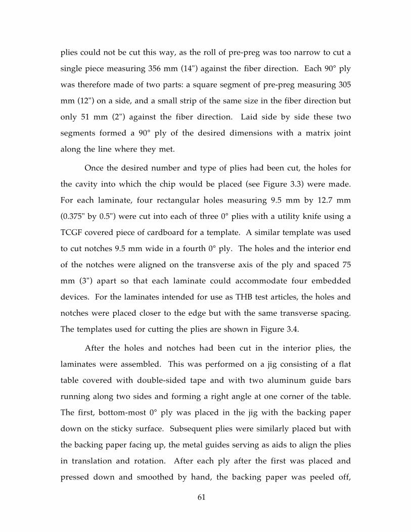
61
plies could not be cut this way, as the roll of pre-preg was too narrow to cut a
single piece measuring 356 mm (14") against the fiber direction. Each 90° ply
was therefore made of two parts: a square segment of pre-preg measuring 305
mm (12") on a side, and a small strip of the same size in the fiber direction but
only 51 mm (2") against the fiber direction. Laid side by side these two
segments formed a 90° ply of the desired dimensions with a matrix joint
along the line where they met.
Once the desired number and type of plies had been cut, the holes for
the cavity into which the chip would be placed (see Figure 3.3) were made.
For each laminate, four rectangular holes measuring 9.5 mm by 12.7 mm
(0.375" by 0.5") were cut into each of three 0° plies with a utility knife using a
TCGF covered piece of cardboard for a template. A similar template was used
to cut notches 9.5 mm wide in a fourth 0° ply. The holes and the interior end
of the notches were aligned on the transverse axis of the ply and spaced 75
mm (3") apart so that each laminate could accommodate four embedded
devices. For the laminates intended for use as THB test articles, the holes and
notches were placed closer to the edge but with the same transverse spacing.
The templates used for cutting the plies are shown in Figure 3.4.
After the holes and notches had been cut in the interior plies, the
laminates were assembled. This was performed on a jig consisting of a flat
table covered with double-sided tape and with two aluminum guide bars
running along two sides and forming a right angle at one corner of the table.
The first, bottom-most 0° ply was placed in the jig with the backing paper
down on the sticky surface. Subsequent plies were similarly placed but with
the backing paper facing up, the metal guides serving as aids to align the plies
in translation and rotation. After each ply after the first was placed and
pressed down and smoothed by hand, the backing paper was peeled off,
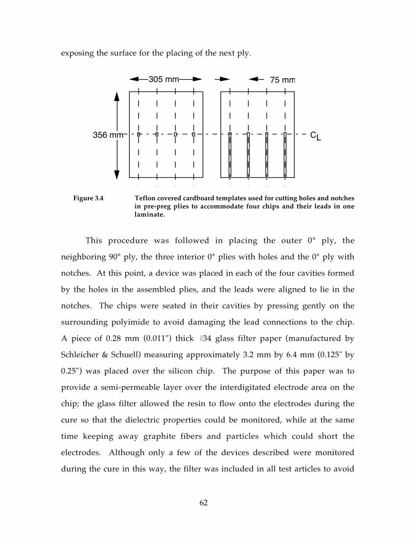
62
exposing the surface for the placing of the next ply.
305 mm
356 mm CL
75 mm
Figure 3.4 Teflon covered cardboard templates used for cutting holes and notchesin pre-preg plies to accommodate four chips and their leads in onelaminate.
This procedure was followed in placing the outer 0° ply, the
neighboring 90° ply, the three interior 0° plies with holes and the 0° ply with
notches. At this point, a device was placed in each of the four cavities formed
by the holes in the assembled plies, and the leads were aligned to lie in the
notches. The chips were seated in their cavities by pressing gently on the
surrounding polyimide to avoid damaging the lead connections to the chip.
A piece of 0.28 mm (0.011") thick #34 glass filter paper (manufactured by
Schleicher & Schuell) measuring approximately 3.2 mm by 6.4 mm (0.125" by
0.25") was placed over the silicon chip. The purpose of this paper was to
provide a semi-permeable layer over the interdigitated electrode area on the
chip; the glass filter allowed the resin to flow onto the electrodes during the
cure so that the dielectric properties could be monitored, while at the same
time keeping away graphite fibers and particles which could short the
electrodes. Although only a few of the devices described were monitored
during the cure in this way, the filter was included in all test articles to avoid

63
introducing undesirable variations. While the glass paper was probably not
needed to prevent shorting of the active electrical components on the devices
with the fairly hard standard protective epoxy layer, it may well have served
this function for the chips covered with the much softer silicone isolation
layer. In either case, the porosity of the glass would not have presented a
barrier to moisture or ionic contaminants.
After placement of the devices and the glass filter paper, the remaining
90° and 0° plies were laid on top of the assembly to complete the layup. The
resulting laminate was then removed from the jig and the remaining pieces
of backing paper were peeled off and replaced by sheets of peel-ply. The peel-
ply layers, permeable nylon sheets manufactured by Burlington Impression
Fabrics, provided a textured finish to the surface of the cured part. Excess
graphite/epoxy and peel-ply were trimmed from the three sides of the
laminate, which was then ready for curing.
3.2.3 Cure assembly
The assembled laminates were cured on an aluminum caul plate. The
caul plate was prepared by coating it with the mold release agent Mold-Wiz
and covering it with a sheet of non-porous teflon coated glass fabric (TCGF).
A T-shaped aluminum dam and an aluminum top plate was positioned on
the caul plate, and strips of adhesive backed corprene rubber (type DK-153T
manufactured by I. G. Marston) were used to hold the aluminum dam in
place and to form the other two sides of the rectangular well in which the
laminate is to be placed, as shown in Figure 3.5. The T-dam and top plates
were removed, and the T-dam was sprayed with the mold release agent
Frekote and replaced on the caul plate.

64
Space forsecond laminate
T-shaped aluminum dam
Corprenerubberstrips
Well forlaminate,top plate
Aluminum caul plate
Figure 3.5 Layout of T-dam and corprene rubber strips on aluminum caul plate toform well for composite laminate.
A diagram illustrating the various components of the cure assembly is
presented in Figure 3.6a. A sheet of non-porous TCGF 25 mm (1") larger than
the laminate on each side was placed in the well and the laminate was placed
on top. At this point allowance had to be made for the leads projecting from
one side of the laminate, as shown in Figure 3.6b. Although the excess fringe
of the peel-ply and non-porous TCGF normally lie on top of the dam, it was
necessary to keep the leads relatively flat to avoid crimping them between the
dam and top plate. Small slits were therefore cut in the peel-ply and
underlying TCGF sheet; the leads ran through these slits and under the
corprene rubber dam, which was temporarily lifted up to allow this. In order
to prevent the corprene rubber dam from adhering to the leads after the cure,
small sleeves of non-porous TCGF were wrapped around the leads.

65
13
4 52
67
9
8
107
11
2
Key: 1. Aluminum Caul Plate2. Non-porous Teflon Coated Glass Fabric3. Vacuum Tape4. Aluminum Dam5. Corprene Rubber Dam6. Laminate Covered with Peel Ply7. Porous Teflon Coated Glass Fabric8. Paper Bleeder9. Aluminum Top Plate10. Glass Cloth Air Breather11. Vacuum Bag
2
2
Figure 3.6a Schematic cross-section of the cure assembly.
The laminate was then covered by an oversize piece of porous TCGF,
followed by four layers of paper bleeder (one for every two plies in the
laminate) to soak up excess resin. Another oversize sheet of TCGF was laid
on top of the bleeder followed by the top plates, which had been coated with
Frekote, and another sheet of TCGF. The entire plate was then covered with
pieces of porous TCGF, followed by a sheet of glass breather cloth. This
provided the air passages necessary for the even application of vacuum to the
assembly. Finally, a bead of vacuum tape was applied along the exposed

66
1
3
3
2
8
5
9
2
6
7
2
Figure 3.6b Detail of routing of leads around corprene rubber dam and throughvacuum tape seal. Legend is that of 3.4a. Note that device leads(heavy line) pass through slits, under corprene rubber dam, and betweenvacuum tape layers.
outside edge of the caul plate and a piece of vacuum bag was placed over the
entire assembly, producing an airtight enclosure open only at the attachment
to the vacuum ports. In order to allow the monitoring of the devices during
the cure, the leads were brought out of the vacuum enclosure by routing
them over the bead of vacuum tape and covering them with a second bead of
tape for the seal to the vacuum bag.
3.2.4 Cure schedule and yields
After the cure assembly was complete, the air within it was evacuated
using a mechanical pump. The vacuum seal was considered sufficiently good
when a vacuum was maintained to within 1" Hg of 29" Hg over five minutes
with the pump shut off. Following successful completion of this test outside
the autoclave, it was repeated inside the autoclave. Then the vacuum was
turned on again and the autoclave was pressurized to 0.59 MPa (85 psig).

67
Upon reaching the desired pressure, the heaters were turned on and the cure
cycle began. The vacuum, pressure, and temperature profiles during the cure
are shown in Figure 3.7.
25
116
177149
Autoclave Temperature (C)
Time (minutes)20 122 36250 110 392
Autoclave Pressure (MPa, gage)
Time (minutes)20 12250 110
0.59
362392
Autoclave Vacuum (MPa)
Time (minutes)20 12250 110
0.10
362392
Figure 3.7 Temperature, pressure, and vacuum histories during the AS4/3501-6graphite/epoxy cure; dashed line is the standard cure, solid is themodified scheduled followed in this work.

68
The two temperature stages perform two functions. During the one
hour hold at 116 C (240 F), the viscosity of the resin decreases and it starts to
flow, allowing the plies to merge and settle under the pressure. The high
temperature stage at 149 C (300 F) drives the epoxy cross-linking reaction to
near completion. The heating is performed by forced air convection past
electric heating coils, and the cooling is effected by passing the air over tubes
containing chilled water. Both the heating and cooling rates are kept to
roughly 3 C/minute (5 F/minute), the latter to prevent the occurrence of
thermal shock.
It should be noted that the standard cure cycle calls for a high
temperature stage of two hours at 177 C (350 F) as opposed the four hours at
149 C (300 F) used in the cures in this work. The conventional profile was
used on the first three trial cures involving ten devices, but six of these
devices were found to fail during the cure, giving a yield of only 40%. Those
failed devices which were monitored during the cure by the Micromet
instrument showed erratic data starting at some point in the high
temperature stage, and measurements of diode drops across some of the leads
with a Fluke 77 multimeter were off scale, indicating open circuits. Since the
resin should have already settled during the low temperature cure stage, and
the temperature was not changing at the time of failure, the phenomenon
could not be explained by mechanical loads induced by mismatch of
coefficients of thermal expansion.
On the hypothesis that the failures might be due to some abrupt change
in the specific volume upon passing through the glassification temperature,
the longer and cooler cycle was tried. Five cures were performed using this
modified schedule. Four of these involved 26 devices with the standard
protective epoxy, of which 15 survived for a yield of 58%, and one cure

69
involved eight devices with the RTV silicone isolation layer, of which three
survived for a yield of 38%.
A final deviation from the standard cure was the omission of an 8
hour post cure at 177 C (350 F) and atmospheric pressure. This post cure is
meant to drive the epoxy reaction still further, producing some increase in
fracture toughness but little change in elastic properties. Since this operation
is generally not performed in industry, and to avoid the possibility of still
further decreases in yields of functional devices, the post cure was eliminated.
Type of Test Type of Test
Article StaticMechanical
CyclicMechanical
Temperature/Humidity/Bias
With epoxy layerE-STAT-1E-STAT-2E-STAT-3
E-CYC-1E-CYC-2E-CYC-3
THB-1THB-2THB-3
With RTV layerR-STAT-1R-STAT-2
R-CYC-1 -
Standard cure,non-functioning
device
NFD-STAT-1NFD-STAT-2
- -
Standard cure, nodevice
ND-STAT-1ND-STAT-2
- -
Table 3.1 List of test articles, ordered by characteristics and type of test.
Table 3.1 presents an overview of all the test articles used in this
investigation and their code designations. Note the inclusion of the four test
articles with non-functioning devices or no devices. These are from the
preliminary trial cures performed with the standard cure schedule, and were
included in the static mechanical tests to provide some indication of the
separate effects that the inclusion of a device and the modified cure might
70
have on the modulus and strength of the coupon.
3.2.5 Machining, loading tabs, and instrumentation
The cured laminates were machined into coupons of the appropriate
sizes using a milling machine fitted with a diamond abrasive disk and a water
jet for cooling and dust removal. The disk rotated at the spindle rate of 1100
RPM, and the table to which the laminates were clamped was translated
under the disk at 200 mm (8") per second. Two kinds of test articles were
machined in this way: those intended for mechanical testing, and those
intended for THB testing.
The mechanical test articles were machined to standard TELAC coupon
dimensions, shown in Figure 3.8. The coupons measured a nominal 356 mm
(14") in length and 50 mm (2") in width. The coupons were milled so that the
device chips were centered both longitudinally and transversely, and the
leads ran half the length of the coupon to emerge at one end. The thickness
of the coupons measured at locations away from the chip varied from 1.04
mm to 1.12 mm (0.041 to 0.044"). The coupons containing the devices with
the standard protective epoxy layer measured 1.14 to 1.17 mm (0.045 to 0.046")
in thickness at the chip location, while the coupons with RTV silicone
isolated devices measured 1.24 mm (0.049"). Since the slight excess resin on
the surfaces tends to give slightly oversized thickness measurements,
especially for thin laminates, while contributing little to the strength or
stiffness, a nominal thickness of 1.07 mm (0.042") was assumed for later stress
calculations.

71
50 mm
356
mm
203
mm
30°
1.08 mm Fiberglassloading tabs
G/E coupon
Fiberglassloading tabs
Embeddedchip
Chipleads
Figure 3.8 Test article for static and cyclic mechanical tests.
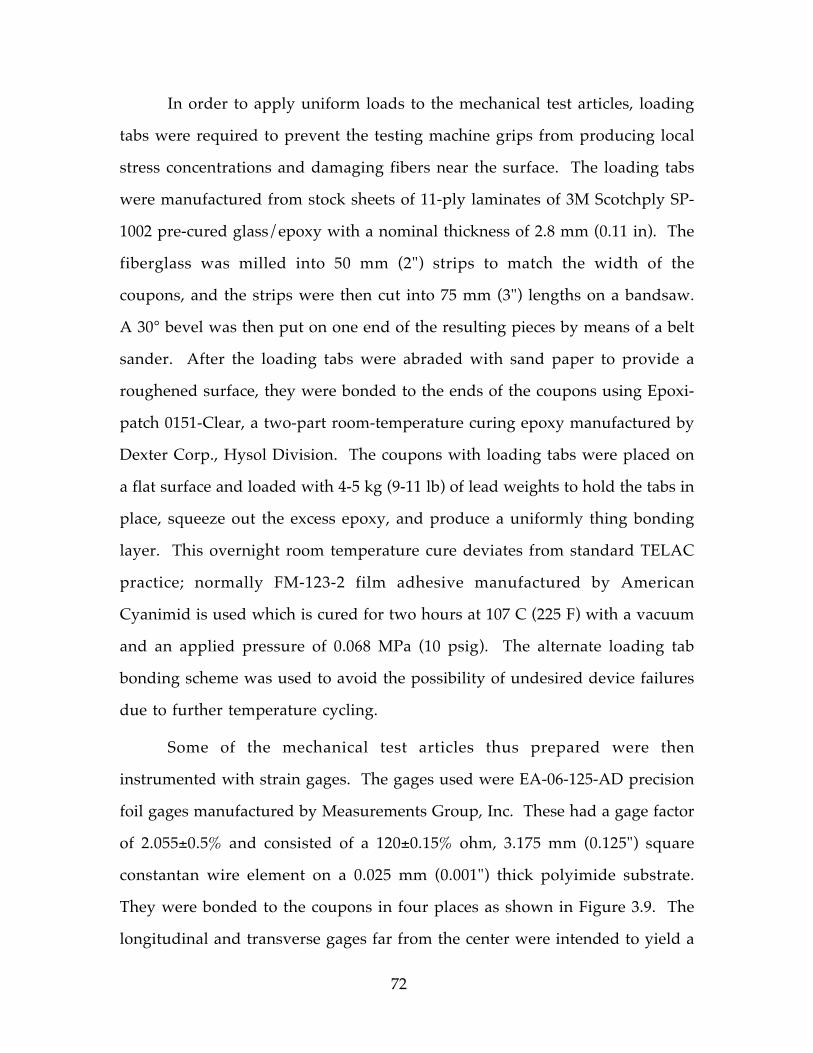
72
In order to apply uniform loads to the mechanical test articles, loading
tabs were required to prevent the testing machine grips from producing local
stress concentrations and damaging fibers near the surface. The loading tabs
were manufactured from stock sheets of 11-ply laminates of 3M Scotchply SP-
1002 pre-cured glass/epoxy with a nominal thickness of 2.8 mm (0.11 in). The
fiberglass was milled into 50 mm (2") strips to match the width of the
coupons, and the strips were then cut into 75 mm (3") lengths on a bandsaw.
A 30° bevel was then put on one end of the resulting pieces by means of a belt
sander. After the loading tabs were abraded with sand paper to provide a
roughened surface, they were bonded to the ends of the coupons using Epoxi-
patch 0151-Clear, a two-part room-temperature curing epoxy manufactured by
Dexter Corp., Hysol Division. The coupons with loading tabs were placed on
a flat surface and loaded with 4-5 kg (9-11 lb) of lead weights to hold the tabs in
place, squeeze out the excess epoxy, and produce a uniformly thing bonding
layer. This overnight room temperature cure deviates from standard TELAC
practice; normally FM-123-2 film adhesive manufactured by American
Cyanimid is used which is cured for two hours at 107 C (225 F) with a vacuum
and an applied pressure of 0.068 MPa (10 psig). The alternate loading tab
bonding scheme was used to avoid the possibility of undesired device failures
due to further temperature cycling.
Some of the mechanical test articles thus prepared were then
instrumented with strain gages. The gages used were EA-06-125-AD precision
foil gages manufactured by Measurements Group, Inc. These had a gage factor
of 2.055±0.5% and consisted of a 120±0.15% ohm, 3.175 mm (0.125") square
constantan wire element on a 0.025 mm (0.001") thick polyimide substrate.
They were bonded to the coupons in four places as shown in Figure 3.9. The
longitudinal and transverse gages far from the center were intended to yield a
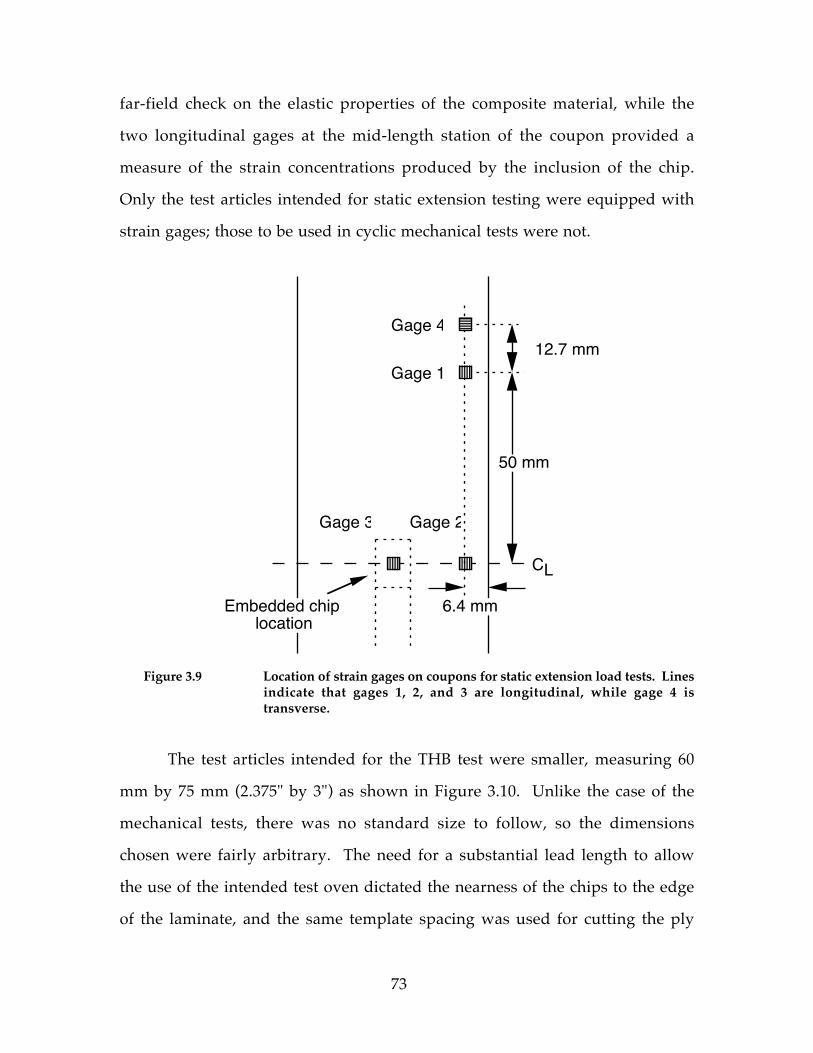
73
far-field check on the elastic properties of the composite material, while the
two longitudinal gages at the mid-length station of the coupon provided a
measure of the strain concentrations produced by the inclusion of the chip.
Only the test articles intended for static extension testing were equipped with
strain gages; those to be used in cyclic mechanical tests were not.
CL
50 mm
12.7 mm
6.4 mmEmbedded chiplocation
Gage 1
Gage 2
Gage 4
Gage 3
Figure 3.9 Location of strain gages on coupons for static extension load tests. Linesindicate that gages 1, 2, and 3 are longitudinal, while gage 4 istransverse.
The test articles intended for the THB test were smaller, measuring 60
mm by 75 mm (2.375" by 3") as shown in Figure 3.10. Unlike the case of the
mechanical tests, there was no standard size to follow, so the dimensions
chosen were fairly arbitrary. The need for a substantial lead length to allow
the use of the intended test oven dictated the nearness of the chips to the edge
of the laminate, and the same template spacing was used for cutting the ply

74
holes and notches as in the laminates intended for use as mechanical test
articles. Since the ratio of length or width to thickness was then
approximately 55-70:1, it could be argued that performance degradation due to
bulk diffusion of moisture and ionic contaminants would be dominated by
travel through the thickness of the test article rather than in the plane. This
argument however does not address the possibility of preferential moisture
migration along the interface between the leads and the composite.
Embedded chiplocation
75 mm
60 mmCL
CL
Figure 3.10 Nominal dimensions of THB test article.
All the THB test articles prepared had embedded devices with the
standard protective epoxy layer rather than the RTV silicone layer. Although
the RTV silicone also provided passivation, it was primarily chosen as a
compliant mechanical isolation layer for comparison with the more rigid
epoxy. The performance of the RTV silicone with respect to protection
against moisture and ionic contamination is relevant, but in this work
additional THB tests on devices embedded with the RTV silicone layer were
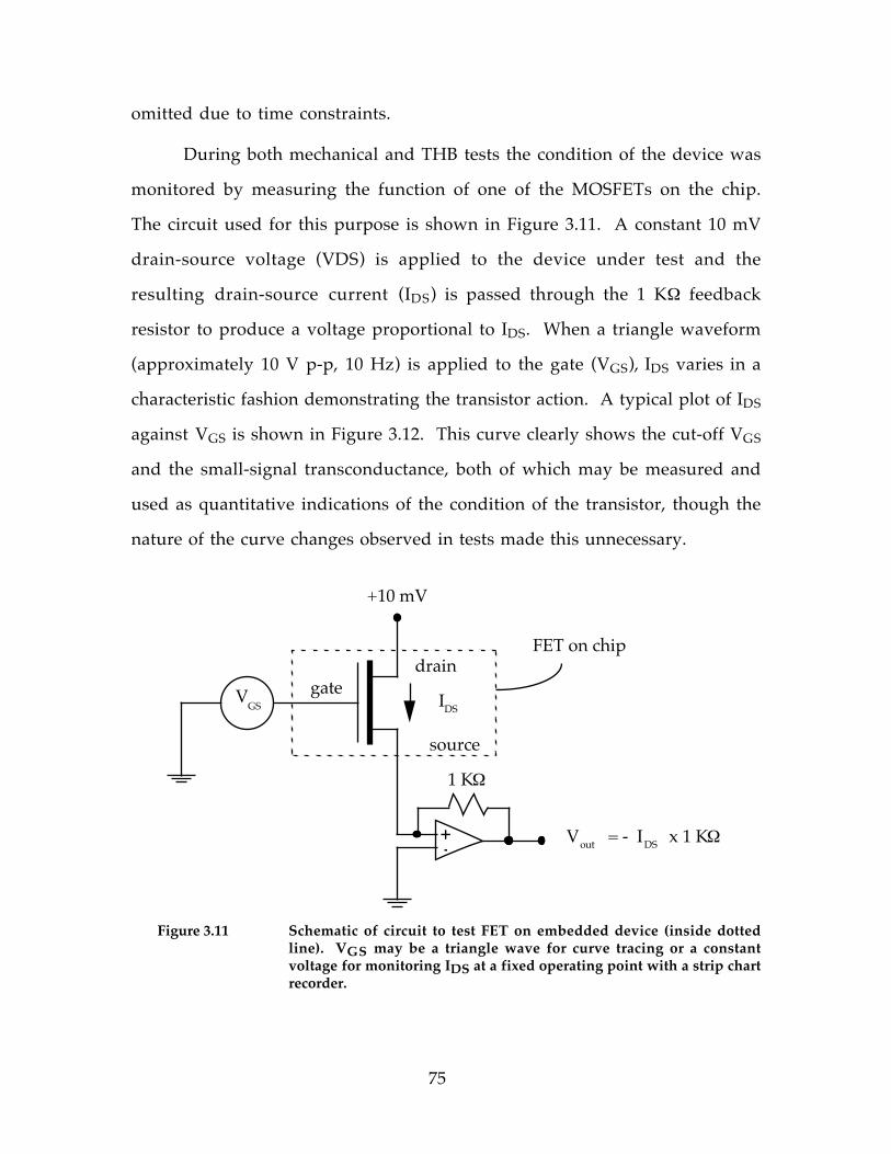
75
omitted due to time constraints.
During both mechanical and THB tests the condition of the device was
monitored by measuring the function of one of the MOSFETs on the chip.
The circuit used for this purpose is shown in Figure 3.11. A constant 10 mV
drain-source voltage (VDS) is applied to the device under test and the
resulting drain-source current (IDS) is passed through the 1 KW feedback
resistor to produce a voltage proportional to IDS. When a triangle waveform
(approximately 10 V p-p, 10 Hz) is applied to the gate (VGS), IDS varies in a
characteristic fashion demonstrating the transistor action. A typical plot of IDS
against VGS is shown in Figure 3.12. This curve clearly shows the cut-off VGS
and the small-signal transconductance, both of which may be measured and
used as quantitative indications of the condition of the transistor, though the
nature of the curve changes observed in tests made this unnecessary.
+10 mV
VGS
drain
source
gateIDS
FET on chip
1 KW
Vout = - x 1 KWIDS+-
Figure 3.11 Schematic of circuit to test FET on embedded device (inside dottedline). VGS may be a triangle wave for curve tracing or a constantvoltage for monitoring IDS at a fixed operating point with a strip chartrecorder.

76
- 5 0
0
5 0
100
150
200
250
300
- 6 - 4 - 2 0 2 4
VGS, V
I DS
, mA
6
transconductance
threshold
Figure 3.12 Typical transistor characteristic curve of drain-source current as afunction of gate-source voltage shows threshold voltage and small-signal transconductance. Drain-source voltage was fixed at 10 mV. Thiscurve was taken on test article THB-3 at 80 C at the start of the test.
Transistor curves obtained with this test circuit were stored on disks
using a Nicolet digital oscilloscope, but this could only provide an
approximately instantaneous picture of the state of the device's electronic
behavior. In order to produce a continuous history of circuit behavior for
tests expected to run for long periods of time, provisions were made to replace
the VGS triangle waveform with a constant voltage. This would produce a
test circuit output voltage proportional to the nominally constant IDS.
Variations in the transistor behavior would then be reflected by changes in
this voltage, which could be continuously plotted for up to four devices using
a four-channel Gould Brush 2400 strip chart recorder with DC amplifiers.
These continuous measurements could be interrupted from time to time to

77
capture complete transistor curve traces using the triangle waveform.
In the next two sections, details are given of tests performed on the test
articles whose preparation and manufacture has just been described. The
performance of the embedded devices under static and cyclic mechanical
loading, with both the standard protective epoxy and RTV silicone layers, is
investigated, followed by testing of susceptibility to damage induced by heat
and moisture in the THB experiment.
3.3 Mechanical Load Tests
Once the capability to produce composite parts with functioning
embedded electronic components has been demonstrated, the application of
such structures as load bearing members immediately raises questions about
the sensitivity of the electronic behavior to applied loads. The basic concern
regarding the function of the embedded devices while the structure is under
load was tested by subjecting the mechanical test articles to an increasing
quasi-static extensional load. The possibility of fatigue failure were explored
by the application of cyclic tension-tension loads. Both of these tests were
expected to indicate failure modes possibly involving lead fracture, lead
debonding, or chip fracture. These tests were further designed to show
whether the transistor function would exhibit an undesirable sensitivity to
strain at any level.
3.3.1 Procedure description
Static extension tests were performed on a total of five test articles with
embedded devices: three with the standard protective epoxy and two with the
RTV silicone isolation layer. Each test article was placed in a MTS 810
Material Test System hydraulic testing machine, and the top and bottom grips
78
were pressurized to 7 MPa (1000 psi). Each of the four strain gages was
connected to a Vishay 2120 strain gage signal conditioner attached to a DEC
PDP 11/34 equipped with A/D converters and running TELAC automatic data
acquisition software. In addition to the strain gage readings, the computer
recorded stroke and load from the actuator and load cell of the MTS machine.
The leads of the embedded device were connected to the transistor test circuit
and the trace of ID S against VG S was monitored on a Nicolet digital
oscilloscope.
After the strain gage amplifiers were balanced and the gripping
pressure was applied, the hydraulic actuator began to apply the extensional
load. The MTS controller was run under stroke control and was programmed
to move the actuator head in a ramp profile to produce an elongation of 12.7
mm (0.5") over a period of 1000 seconds. The computer recorded load, stroke,
and the four strain readings once every 0.5 seconds for the duration of the
test. Transistor curve traces were recorded on magnetic disk before and after
gripping. During the loading, traces were recorded every 15 seconds through
the first 90 seconds and every 30 seconds thereafter. Additional traces were
recorded at unscheduled times when noticeable changes occurred in the
transistor curve. At each recording of the transistor curve a mark was placed
in the data recorded by the computer so that both scheduled and unscheduled
traces could be correlated with the concurrent applied load and strain gage
readings.
During the first round of tests of the test articles with the standard
epoxy layer, the MTS machine was allowed to continue until gross damage to
the laminate was visible and the load level dropped substantially, at which
point the controller and data acquisition system were halted. This was done
to establish the ultimate strength of the coupons for comparison with the
79
loads at which the embedded devices failed. As this resulted in the complete
fragmentation of the silicon chips and the destruction of their delicate lead
connections, subsequent examination of the test articles could yield no
additional information regarding the failure mechanism of the devices. To
allow such analysis, an attempt was made to stop the tests of the test articles
with the RTV silicone layer prior to the complete breaking of the coupons.
These tests were stopped shortly after cessation of device function.
Cyclic extension tests were performed on a total of four test articles
with embedded devices: three with the standard protective epoxy and one
with the RTV silicone isolation layer. Each test article was placed in a MTS
810 Material Test System hydraulic testing machine, and the top and bottom
grips were pressurized to 7 MPa (1000 psi). The leads of the embedded device
were connected to the transistor test circuit and the trace of IDS against VGS
was monitored on a Nicolet digital oscilloscope.
As is usual in fatigue tests and in contrast to the procedure followed in
the static tests, the computer data acquisition system was not used to record
stroke, load, or strain. Since a large number of cycles (perhaps hundreds of
thousands) were originally expected to be completed, data from such
measurements would have been so repetitious as to have been meaningless.
Instead, a procedure more like that employed in the corrosion test was
planned. Since fatigue phenomena generally tend to follow patterns based on
the log of the number of cycles (as suggested by the semi-logarithmic scales
used in standard S/N diagrams) it was decided to record transistor curve
traces on a roughly logarithmic scale, after the first cycle, the third cycle, the
tenth cycle, the thirtieth cycle, and so on. During long periods of cycling the
behavior of the circuits would be monitored by recording the ID S
measurement on the strip chart recorder while under constant VGS bias.

80
The mechanical loading was in the form of a tension-tension
haversine. The test article, once fixed in the grips, was pre-loaded to a tension
corresponding to 1/10 of the maximum to be applied, and the MTS controller
was then programmed to apply a sinusoidal tensile load varying between this
starting level and the maximum. The maximum load was originally chosen
to correspond to a nominal tensile stress of 540 MPa (77 ksi) based load levels
associated with device failures observed in the static tensile tests. This level
and the corresponding 10% minimum load was lowered on some of the later
cyclic tests to 410 and 41 MPa (60 and 6 ksi), respectively, in an attempt to
obtain more cycles before failure. In each test, the first cycle was performed at
0.01 Hz, the next nine at 0.1 Hz, and all subsequent cycles at 1.0 Hz.
3.3.2 Results
In this section, the results of first the static and then the cyclic
mechanical tests will be presented. The effectiveness of the RTV silicone
layer in increasing the attainable loads and number of cycles is demonstrated.
In addition, the effect of the presence of the chip and leads on the strength
and stiffness of the coupons is indicated. An explanation of the device failure
mechanism is given, as are the loads and numbers of cycles at which these
failures occur.
One of the major objectives of these tests was to observe the behavior
of the embedded device when placed under mechanical stress. In all cases,
the transistor characteristic curves observed and recorded on the digital
oscilloscope showed no dependence on load levels, such as might be due to
lead resistance changes with elongation or other gradual effects. The devices
themselves did not act as strain gages, and appeared to be insensitive to the
load applied to the coupon until device failure. The appearance and nature of

81
the failure behavior is described below in some detail following the cyclic test
results; generally speaking, it manifested itself in both the static and cyclic
tests as a sudden replacement of the characteristic curve (like that in Figure
3.12) with a horizontal flat line at or close to zero.
The plots in Figure 3.13 show the load levels at which the embedded
devices failed in test articles E-STAT-1, 2, and 3, all of which incorporated
devices with the standard protective epoxy layer. The device in E-STAT-1
performed properly up to 7700 mstrain and 750 MPa, which are 57% and 71%
of the maximum values of 13500 mstrain and 1050 MPa. E-STAT-2 functioned
up to 9000 mstrain and 1010 MPa, 64% and 83% of the maximum values of
14000 mstrain and 1220 MPa, while E-STAT-3 survived only until 2300 mstrain
and 260 MPa, 16% and 22% of the maximum values of 14200 mstrain and 1180
MPa.
In each case, cracking sounds were heard around 250 MPa (2400
mstrain), possibly indicating matrix failure. Visible laminate damage first
appeared near maximum load in the form of fiber breakage in the outer 0°
plies at the chip location, and concluded with the complete fracture of the
coupon along the transverse centerline. At the end of such a test, the
coupons were damaged to such an extent that the embedded chips were
visible and appeared to be shattered. Further tests to determine the exact
mode of device failure were therefore impossible.

82
0 2500 5000 7500 10000 12500 15000
0
200
400
600
800
Str
ess
(M
Pa
)E -STAT - 1
1000
1200
1400
gage 1 gage 2 gage 3
Strain (mstrain)
device failure at 1010 MPa
Figure 3.13a Stress-strain curves of static tension test article E-STAT-1.Longitudinal strain at three locations is shown along with the loadlevel at which transistor function ceased.
0 2500 5000 7500 10000 12500 15000
0
200
400
600
800
1000
1200
1400
Str
ess
(M
Pa
)
E -STAT - 2
gage 1 gage 2 gage 3
device failure at 750 MPa
Strain (mstrain)
Figure 3.13b Stress-strain curves of static tension test article E-STAT-2.

83
0 2500 5000 7500 10000 12500 15000
0
200
400
600
Str
ess
(M
Pa
)E -STAT - 3
800
1000
1200
1400
gage 1 gage 2 gage 3
Strain (mstrain)
device failure at 260 MPa
Figure 3.13c Stress-strain curves of static tension test article E-STAT-3.
Also shown on the plots in Figure 3.13 are three longitudinal stress-
strain curves of each of the test articles. The strain values are those from the
strain gages 1, 2, and 3, placed as shown in Figure 3.9, while the stress values
were computed by dividing the applied load by a nominal cross-sectional area
of 5.4x10⁻⁵ m2. In all cases, the longitudinal strain measured to the side of the
chip and that measured in the far field are close, while the strain measured
directly over the chip shows a strain concentration of from 1.6 to 2.3, with a
variation possibly due to the difficulty of repeatability in the placement of the
gage directly over the chip. These results suggest that the disturbance in the
otherwise uniform stress and strain fields caused by the inclusion of the chip
is a very localized one and that the ratio of coupon width to device package
width of approximately 5.3 :1 was sufficient to exclude significant interaction
between the strain in the vicinity of the chip and the strain near the free edges

84
of the coupon.
The stress-strain plots from the static tensile tests of the two test articles
with the RTV silicone isolation layer, R-STAT-1 and 2, are shown in Figure
3.14. The overall appearance of these curves is similar to those obtained from
the tests of test articles with the standard epoxy layer shown in Figure 3.13.
The comparison of the strain measurements from the gages directly over the
embedded device location with those from the gages further away shows
localized strain concentrations of 1.8 and 1.9 over the device, also similar to
those observed in the previous tests.
0 2500 5000 7500 10000 12500 15000
0
200
400
600
800
1000
1200
Str
ess
(M
Pa
)
R -STAT - 11400
gage 1 gage 2
device failure at 1030 MPa
Strain (mstrain)
gage 3
Figure 3.14a Stress-strain curves of static tension test article R-STAT-1.Longitudinal strain at three locations is shown along with the loadlevel at which transistor function ceased.
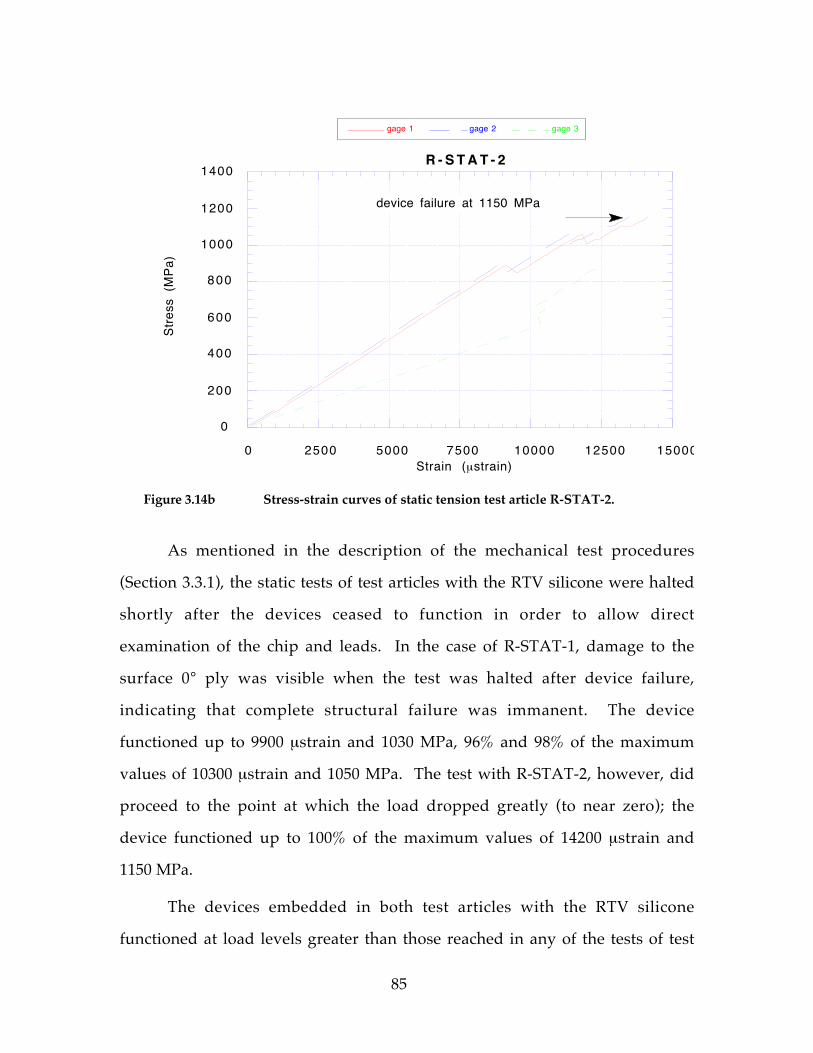
85
0 2500 5000 7500 10000 12500 15000
0
200
400
600
Str
ess
(M
Pa
)R -STAT - 2
800
1000
1200
1400
gage 1 gage 2 gage 3
Strain (mstrain)
device failure at 1150 MPa
Figure 3.14b Stress-strain curves of static tension test article R-STAT-2.
As mentioned in the description of the mechanical test procedures
(Section 3.3.1), the static tests of test articles with the RTV silicone were halted
shortly after the devices ceased to function in order to allow direct
examination of the chip and leads. In the case of R-STAT-1, damage to the
surface 0° ply was visible when the test was halted after device failure,
indicating that complete structural failure was immanent. The device
functioned up to 9900 mstrain and 1030 MPa, 96% and 98% of the maximum
values of 10300 mstrain and 1050 MPa. The test with R-STAT-2, however, did
proceed to the point at which the load dropped greatly (to near zero); the
device functioned up to 100% of the maximum values of 14200 mstrain and
1150 MPa.
The devices embedded in both test articles with the RTV silicone
functioned at load levels greater than those reached in any of the tests of test

86
articles with the epoxy layer. This suggests that although it did not
completely enclose the chip, the RTV layer was in fact successful in
performing its mechanical isolation function and alleviating the stress
concentrations causing damage to the chip or its leads. No other noticeable
changes were observed in the appearance or mechanical behavior of the
coupon as a result of the difference in protective layer, aside from the
previously mentioned 7% increase in coupon thickness at the embedded
device location.
Because of the fragility of the chips and leads without the standard
epoxy layer, the preparation of the test articles with the RTV silicone was
rather difficult, and only a few were produced. In view of the apparent
success of the RTV silicone in the static tests, the originally planned third
static test was abandoned, and the last mechanical test article with the RTV
silicone was instead employed in a cyclic test.
The results of the static mechanical tests are summarized in Table 3.2.
As previously noted (Section 3.2.4), three trial cures were performed using the
standard 350 F TELAC cure for AS4/3501-6 before switching to the modified
300 F cure schedule. Maximum stress and modulus data for some coupons
from these trial cures have been included in the table for comparison. Of
these test articles, two included an embedded (though non-functioning)
device, and two were essentially blanks with the [0°/90°/0°2]S layup but with
neither the embedded device nor the modifications (holes and slots cut in
interior plies) necessary to accommodate a device.

87
Test articletype
Device Failure
Strain Stress
Laminate Maximum
Strain Stress
Long.Elastic
Modulus(mstrain) (MPa) (mstrain) (MPa) EL (GPa)
E-STAT-2 7700 750 13500 1050 97E-STAT-1 9000 1010 14000 1220 113E-STAT-3 2300 260 14200 1180 101R-STAT-1 9900 1030 10300 1050 109R-STAT-2 14200 1150 14200 1150 99
NFD-STAT-1 - - - 1270 108NFD-STAT-2 - - - 1310 117ND-STAT-1 - - - 1420 105ND-STAT-2 - - - 1630 113
Table 3.2 Comparison of results from static extension tests of test articles withand without RTV silicone isolation layer, as well as standard curecoupons with and without embedded devices.
It should be noted that among the four samples with the standard cure,
the presence of the device appears to have had no effect on the longitudinal
elastic modulus, though the maximum stress is decreased by some 15%. The
use of the non-standard cure described above shows an additional reduction
in maximum stress of about 10% and a decrease in modulus of 5%. The large
scatter in the measurements and the small size of the samples make these
values rather tentative. Considering that in the vicinity of the embedded
device half of the plies (4 of 8) and two thirds (4 of 6) of the 0° axial load
bearing plies are interrupted, this is a modest reduction in strength.
The cyclic tests described in Section 3.3.2 were performed on test articles
like those used in the static tests; three had the standard epoxy layer (E-CYC-1,
2, and 3) and one had the RTV silicone isolation layer (R-CYC-1). The test
articles were subjected to tension-tension loads varying sinusoidally between
10% and 100% of a maximum stress level, which was set to roughly 40-50% of
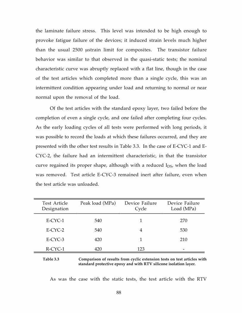
88
the laminate failure stress. This level was intended to be high enough to
provoke fatigue failure of the devices; it induced strain levels much higher
than the usual 2500 mstrain limit for composites. The transistor failure
behavior was similar to that observed in the quasi-static tests; the nominal
characteristic curve was abruptly replaced with a flat line, though in the case
of the test articles which completed more than a single cycle, this was an
intermittent condition appearing under load and returning to normal or near
normal upon the removal of the load.
Of the test articles with the standard epoxy layer, two failed before the
completion of even a single cycle, and one failed after completing four cycles.
As the early loading cycles of all tests were performed with long periods, it
was possible to record the loads at which these failures occurred, and they are
presented with the other test results in Table 3.3. In the case of E-CYC-1 and E-
CYC-2, the failure had an intermittent characteristic, in that the transistor
curve regained its proper shape, although with a reduced IDS, when the load
was removed. Test article E-CYC-3 remained inert after failure, even when
the test article was unloaded.
Test ArticleDesignation
Peak load (MPa) Device FailureCycle
Device FailureLoad (MPa)
E-CYC-1 540 1 270
E-CYC-2 540 4 530
E-CYC-3 420 1 210
R-CYC-1 420 123 -
Table 3.3 Comparison of results from cyclic extension tests on test articles withstandard protective epoxy and with RTV silicone isolation layer.
As was the case with the static tests, the test article with the RTV

89
silicone exhibited a greater tolerance for mechanical loading, failing only after
a total of 123 cycles. This test article showed an intermittent failure similar to
that of E-CYC-1 and E-CYC-2. In post-failure tests, it was observed that the
transistor characteristic curve returned completely to its nominal form when
the test article was unloaded. When the load was reapplied and slowly
increased to around 160 MPa, the curve was replaced by the flat line; after a
few seconds or minutes the curve would begin to reappear intermittently,
becoming more distinct and approaching its nominal form, as illustrated in
Figure 3.15.
- 1 0 0
0
100
200
300
400
500
- 6 - 4 - 2 0 2VGS, V
I DS
, m
A
4 6
a
b
c
Figure 3.15 Transistor characteristic curves of R-CYC-1 during cyclic test. Curve (a)shows the nominal, undamaged behavior; flat line curve (b) shows lossof detectable current under load after fatigue failure; curve (c) showsgradual recovery of transistor behavior during relaxation under tension.
Based on the information gathered from these mechanical tests, it
appears that the failure mode of the device is almost certainly one of lead
breakage or lead debonding. This conclusion is based on experience gained

90
during the curing process, interpretation of the transistor characteristic curve
traces and supporting measurements of diode drops across leads, and direct
examination of cured and uncured devices.
Failure of the devices in all static tests was abrupt and unmistakable;
the typical transistor characteristic curves appeared to instantly change during
the loading ramp to be replaced by flat lines. This would be consistent with
breaking of the drain or source leads, with the shearing off of the oxide and
metal layers on the silicon chip, or with the fracture of the silicon chip itself.
In all cases but one, the chips in these tests were destroyed along with the
coupons, so that these possibilities could not be distinguished.
In the case of R-STAT-1, though, the test was halted before the
complete fracture of the coupon. Some pairs of leads, which normally would
show either low resistance conduction or a diode drop, showed open circuits,
but it was possible to measure a conduction current between the leads to the
common drain and the source of the device's signal transistor. These results
are consistent with the interpretation that the chip and its structures
remained intact, but that most of the leads had broken or debonded. Had the
chip itself or the oxide or metal layers broken, it is unlikely that any leads
would have shown anything other than an open circuit.
The results obtained from the cyclic tests also are consistent with the
presence of a lead failure mode. The intermittent nature of the failures
observed would hardly have been possible had the chip or its structures
broken. The integrity of the field effect transistor, once violated by the
physical fracture of the silicon or by the shearing off of the gate oxide or
metallization layers, could not have been restored by simply bringing the
fragments back in to contact by removing the load. Such a renewal of

91
function could, however, be the result of bringing back into contact the two
ends of a fractured lead, or the end of a debonded lead and its bonding pad. In
these cases, the situation is merely that of a faulty connection; when the two
metallic part are reconnected, the circuit functions as it should.
The curves obtained from the cyclic test of R-CYC-1 shown in Figure
3.15 may be explained by the presence of lead breakage or debonding. When
the connection to the transistor drain or source is solid, curve (a) results;
when it is completely broken, curve (b). The gradual recovery of the signal
under load, curve (b), may be the result of the creep of the RTV silicone layer;
as it relaxes, the metal parts are brought back into contact. In the cyclic tests of
E-CYC-1 and E-CYC-2, it was noted that the curve which reappeared upon
unloading had the general form of the nominal behavior, but showed a
reduced IDS. Since the device was operated at a constant VDS of 10 mV this
could be interpreted as an increased resistance, possibly due to the plastic
deformation of a copper drain or source lead, or to a reduced contact area
either between two broken ends of a lead or between a lead and its contact
pad.
In order to gain further insight into the possible cause of device failure,
direct examinations were made of several embedded devices, specifically E-
CYC-1, R-CYC-1, and R-STAT-1, as well as of a device which had failed during
an unmodified, high temperature cure as described in Section 3.2.3. In each
case, the test article was soaked for several hours in concentrated nitric acid to
etch away the greater part of the surrounding structural epoxy. When the
surface of the chip was largely exposed, a methyl ethyl ketone (MEK) solution
was used to soften the protective epoxy layer, which was then carefully
removed under a microscope with use of small picks and brushes. In the case
of the devices with the RTV silicone layer, a mixture of methylene chloride,

92
methanol, and toluene (5f5 from Sterling-Clark-Lurton Corp.) served the
same purpose.
In all of the examinations the silicon chip itself appeared to be intact.
In test articles E-CYC-1 and R-STAT-1, several leads were observed which had
apparently become bonded from the chip. The device in test article R-CYC-1
showed both loose bonds and cracks completely severing some of the leads.
The fact that the apparently debonded leads were intact and unbent would
seem to be indicative of damage occurring before the stripping for
examination; otherwise the delicate copper leads would have been deformed.
The examination of the failed device cured according to the standard cure
schedule also revealed two partially cracked leads, as well as one debonded
lead. The appearance of a typical crack is shown in Figure 3.16.
copper lead
aluminumbonding pad
cracks
silicon chip
Figure 3.16 Illustration of location of typical crack in copper lead near bond to chip.Examination was performed on unembedded chip.
Since the damage observed could have been incurred during the
removal of the surrounding epoxy, an examination was also made of some
93
devices before embedding, both with and without the standard protective
epoxy applied by the manufacturer. In both cases, cracks were found in the
leads similar to those observed in the test articles. These observations tend to
support the idea that the leads were the weak link in the mechanical tests as
well as during the cure, especially in view of the pre-existing flaws, which
might well account for both the static and cyclic test articles which failed at
low load levels.
In this section, the procedure and results of mechanical tests of the
embedded devices were described. The static tests of the test articles with the
standard protective epoxy showed a degree of success for the method for
embedding described in Section 3.2. The devices were insensitive to the
increasing applied load until failure, which occurred in one case as low as
22% of the maximum coupon load. Indirect evidence and direct examination
indicated lead cracking or debonding (or both) as the most likely device
failure mode.
The test articles with the RTV silicone isolation layer proved more
durable, suggesting that the isolation layer was successful in relieving strain
transfer to the leads and chip and thus postponing device failure to load
levels at which the composite coupon itself completely broke. This layer was
also effective in increasing the number of cycles withstood in the cyclic tests
from 4 or fewer to 123. Though the number of tests was too small to yield
statistically reliable values for reliability predictions, they were sufficient to
demonstrate the success of the embedding technique, the device failure mode,
and the effectiveness of a means for combating that failure mode.
3.4 Temperature-Humidity-Bias Test

94
The remaining test performed on the embedded devices was a
temperature-humidity-bias (THB) test. The devices were subjected to a high
temperature, high humidity environment while being operated at a constant
operating point or bias. The purpose was to check for changes in transistor
behavior as an indication of corrosion due to excessive moisture absorption
or ionic contamination from the structural epoxy. Conventionally packaged
control devices were tested concurrently for comparison of results to the
reliability of commercially available products.
3.4.1 Procedure description
This test was performed on three test articles THB-1, 2, and 3, the
manufacture of which was described in Section 3.2. The test articles were
placed in a Blue M AC-7402HA-1 environmental chamber which was
equipped to maintain a constant temperature of 80 C (176 F) and a constant
relative humidity of 80%. The flexible copper/Kapton leads of the test
articles, which were run between the door and the wall of the chamber
without significantly disturbing the chamber seal, were attached to test
circuits which provided the necessary support both to monitor IDS under
constant bias conditions and to record transistor characteristic curves such as
the one in Figure 3.12 at intervals spaced roughly logarithmically in time,
according to the schedule shown in Figure 3.17. The entire test lasted for 7500
minutes (125 hours), not counting the hour required to bring the chamber
temperature and humidity up to the specified test conditions.

95
1 0 100 1000 10000
end of test at 7500 min.
log. spaced traces
additional traces
Time, min.
Figure 3.17 Plot of the times at which transistor characteristic curves wererecorded during the THB test.
Since the later intervals between curve measurements became rather
long, supplementary curve records were taken at convenient times during
the day. At all other times, the constant bias transistor behavior was
monitored by means of the strip chart recorder as described previously.
Although the purpose of this experiment, like the others, was not to
establish statistically valid estimates of such performance characteristics as
mean lifetime, but rather to seek out possible failure modes, it was deemed
sensible to include in the test a means of providing some measure of
comparison with commercial devices. To this end two control devices were
tested along with the embedded devices. As the closest analog to the devices
under test, a MOSFET in a plastic package, was not available, the controls
chosen were a junction FET (JFET) in a plastic package and a MOSFET in a
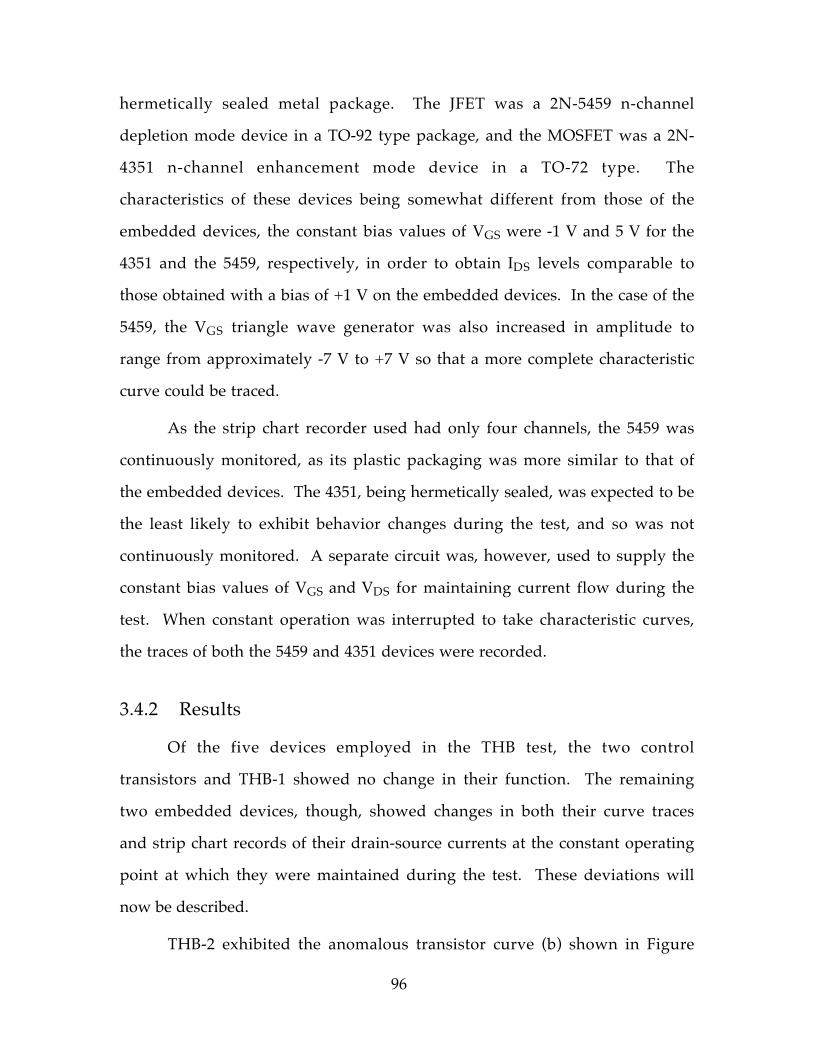
96
hermetically sealed metal package. The JFET was a 2N-5459 n-channel
depletion mode device in a TO-92 type package, and the MOSFET was a 2N-
4351 n-channel enhancement mode device in a TO-72 type. The
characteristics of these devices being somewhat different from those of the
embedded devices, the constant bias values of VGS were -1 V and 5 V for the
4351 and the 5459, respectively, in order to obtain IDS levels comparable to
those obtained with a bias of +1 V on the embedded devices. In the case of the
5459, the VGS triangle wave generator was also increased in amplitude to
range from approximately -7 V to +7 V so that a more complete characteristic
curve could be traced.
As the strip chart recorder used had only four channels, the 5459 was
continuously monitored, as its plastic packaging was more similar to that of
the embedded devices. The 4351, being hermetically sealed, was expected to be
the least likely to exhibit behavior changes during the test, and so was not
continuously monitored. A separate circuit was, however, used to supply the
constant bias values of VGS and VDS for maintaining current flow during the
test. When constant operation was interrupted to take characteristic curves,
the traces of both the 5459 and 4351 devices were recorded.
3.4.2 Results
Of the five devices employed in the THB test, the two control
transistors and THB-1 showed no change in their function. The remaining
two embedded devices, though, showed changes in both their curve traces
and strip chart records of their drain-source currents at the constant operating
point at which they were maintained during the test. These deviations will
now be described.
THB-2 exhibited the anomalous transistor curve (b) shown in Figure

97
3.18. This change was first noted in the trace recorded at 860 minutes into the
7500 minute test, and could be reproduced by testing the same device on
another curve tracing circuit, showing that the effect was a change in the
device, not merely a problem with a specific testing circuit. The change was
intermittent and the curve returned to normal a few minutes later. The
anomaly reappeared in the traces recorded at 3140 and 3540 minutes. At 3540
minutes, measurements were made with the diode indicator of the
multimeter of the voltage drops appearing at several leads with respect to the
substrate. Each voltage drop during the appearance of the anomaly was
slightly elevated above the value measured during normal operation of the
device, and above the corresponding values measured on another properly
operating test device. The anomaly was not observed in later traces.
Comparison of the anomalous curve (b) with the nominal curve (a) in
Figure 3.18 shows, in addition to the obvious hysteresis and substantial non-
zero current for VGS below the threshold voltage, a slight elevation of ID S
when the transistor is turned on. Since the constant bias operating point
during the test held VGS at 1 V, this change was also faintly visible on the
strip chart. Although a change of this small magnitude in the trace could also
be caused by electrical interference by nearby machinery, periods of what
appeared to be elevated IDS occurred intermittently throughout the trace for
this device during the test, the earliest beginning at 275 minutes and lasting
for about 12 minutes.
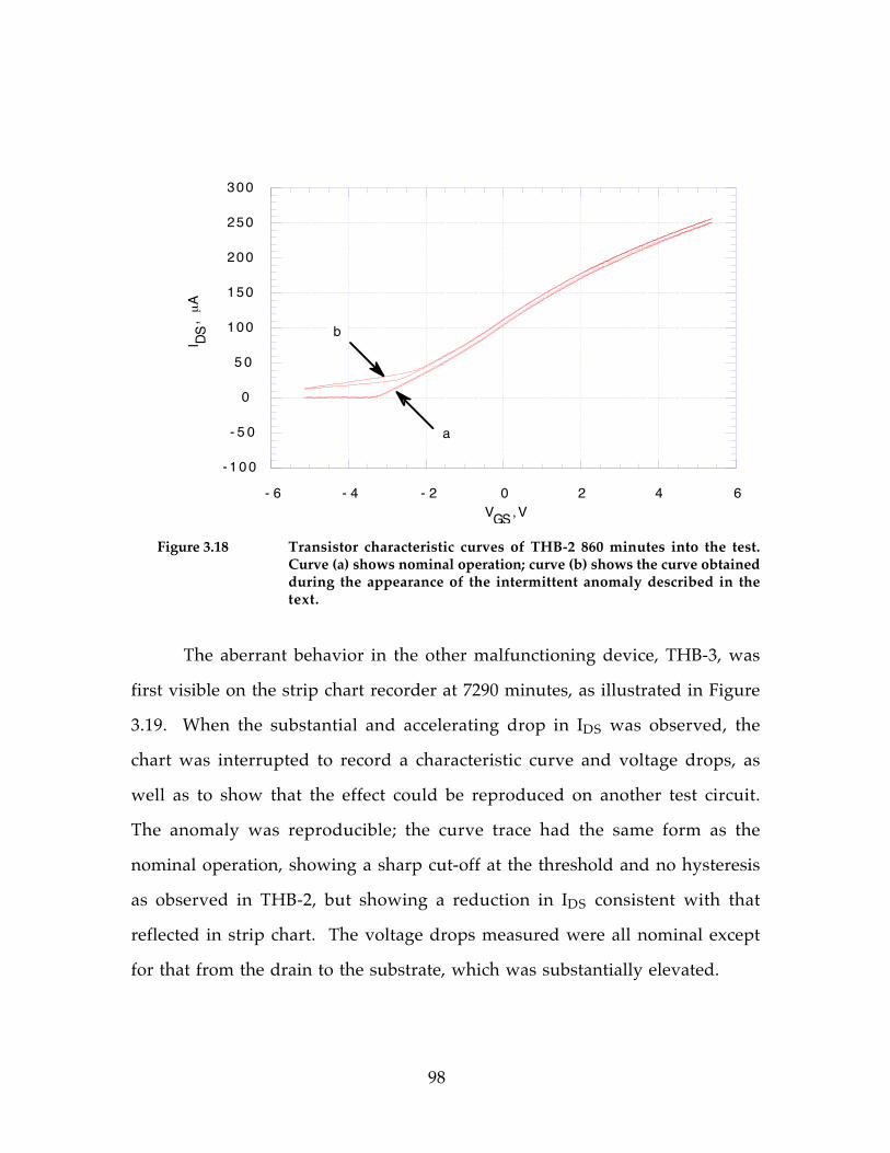
98
- 1 0 0
- 5 0
0
5 0
100
150
200
250
300
- 6 - 4 - 2 0 2VGS,V
I DS
, m
A
a
4 6
b
Figure 3.18 Transistor characteristic curves of THB-2 860 minutes into the test.Curve (a) shows nominal operation; curve (b) shows the curve obtainedduring the appearance of the intermittent anomaly described in thetext.
The aberrant behavior in the other malfunctioning device, THB-3, was
first visible on the strip chart recorder at 7290 minutes, as illustrated in Figure
3.19. When the substantial and accelerating drop in IDS was observed, the
chart was interrupted to record a characteristic curve and voltage drops, as
well as to show that the effect could be reproduced on another test circuit.
The anomaly was reproducible; the curve trace had the same form as the
nominal operation, showing a sharp cut-off at the threshold and no hysteresis
as observed in THB-2, but showing a reduction in IDS consistent with that
reflected in strip chart. The voltage drops measured were all nominal except
for that from the drain to the substrate, which was substantially elevated.

99
-50
0
50
100
150
200
7250 7300 7350 7400 7450 7500
I DS
, mA
Time, min.
Figure 3.19 Time history of source-drain current for THB-3 near the end of the THBtest. Decay of IDS under constant operating conditions is consistentwith gradual degradation of the copper-aluminum bonding of the drainor source leads. Gaps at arrows indicate points at which strip-chartwas disconnected and curve traces were taken.
Both of the anomalies described above could be accounted for by
degradation of one or more lead bonds. In the case of THB-2, the elevated
voltage drop readings for all leads with respect to that attached to the substrate
suggests that the substrate lead itself was faulty. This was supported by later
experimentation by attaching a normal, unembedded device to a curve
tracing circuit but leaving the lead bonded to the substrate disconnected from
the reverse-bias voltage source, thus simulating the effects of a discontinuity
in the substrate lead; a curve similar to (b) in Figure 3.18 was produced.
Fracture of the copper lead itself seems unlikely, since any thermal expansion
(and attendant strain) of the test article would have been completed during
the warm-up, long before the fault appeared. Lead stress could, however,

100
have been due to a slow absorption of moisture by the test article. Another
possible explanation would involve some corrosion mechanism at the
junction of the copper lead and the aluminum bonding pad. Progressive
degradation of this connection could have interrupted the substrate biasing,
while crumbling and shifting of the remaining parts of the copper lead could
explain the intermittent nature of the anomaly.
A similar explanation may be invoked to account for the behavior of
THB-3. In this case, the voltage drop measurements clearly indicate a
problem with the lead or bond associated with the MOSFET drain.
Degradation of this connection could manifest itself as an apparent increase
in resistance; in the presence of a fixed VDS, this would be translated in to a
proportionally reduced IDS. The gradual onset of this condition as shown in
Figure 3.19 is consistent with a progressive corrosion of the copper-
aluminum bond. The partial recovery at 7340 minutes and the pause at 7475
minutes may be due to the crumbling and shifting suggested as an
explanation for the intermittent nature of the behavior of THB-2.
A direct inspection like that described in Section 3.3.2 was made of the
devices in test articles THB-1, 2, and 3. Articles THB-2 and 3 both exhibited
several weak or broken bonds, and THB-3 also had noticeable cracks across
some of its leads. The leads of THB-1 also seemed to be rather fragile, possibly
indicating a degree bond degradation prior to the stage at which electronic
behavior is affected.
In this section, the procedure and results of temperature-humidity-bias
tests of the embedded devices were described. Two of the three devices tested
showed anomalous behavior before the end of the 7500 minute test, while the
third test article and both control devices showed no deviations in function.

101
The behavior of the failed devices was consistent with corrosive damage to
the leads or lead bonds, and weaknesses were observed in these areas by direct
inspection of the devices. This suggests that reliability could possibly be
improved by thickening the fragile copper leads and strengthening the bonds,
which would also be likely to improve the performance of the devices under
mechanical loads.

Related Documents