EMBEDDED CAPACITANCE Presented by Scott Piper, General Motors with special acknowledgement to Gentex corporation

Welcome message from author
This document is posted to help you gain knowledge. Please leave a comment to let me know what you think about it! Share it to your friends and learn new things together.
Transcript

EMBEDDED CAPACITANCE
Presented by
Scott Piper, General Motors with special acknowledgement to Gentex corporation

Case for Embedded Capacitance2
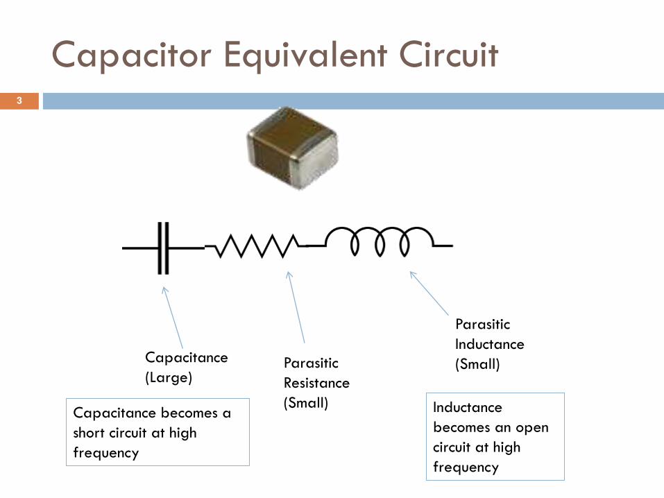
Capacitor Equivalent Circuit
Capacitance
(Large)
Parasitic
Inductance
(Small)Parasitic
Resistance
(Small)Capacitance becomes a
short circuit at high
frequency
Inductance
becomes an open
circuit at high
frequency
3

Impedance vs. Frequency
1µF 0603 Capacitor
Self Resonant
Frequency
4

Real Estate
As designs become
more complex and
microprocessors are
required to do more,
space near an IC is at
a premium
To make things worse,
microprocessor speeds are
increasing requiring low impedance
PDN at high frequency
5

Concept of embedded capacitance6

Parallel Plates Separated by Dielectric
+ + + + + + + + + + + + + + + + + + + + + + + + + + + +
- - - - - - - - - - - - - - - - - - - - - - - - - - - - - - - - - - - - - - - - - - - -
Permittivity
Of Dielectric Plate Area
Plate
Separation
d
Capacitance
7

Multi-layer PCBs
Most PCBs are a
standard thickness
More layers in a PCB
require the layers to
be closer together
This results in more
capacitance between
layers
8

Methodology9

Experimental PCB
PCBs were designed and manufactured for embedded capacitance research
Various Dimensions
4 Layer (two planes and two signal layers)
Most are FR4 cores
Various spacing between planes

Measurement Methodology11
Network Analyzer
Port 1
Z11 was measured
to determine power
distribution network
(PDN) Impedance
PCB
A PCB mounted
coaxial connector was
used to connect the
planes to the network
analyzer
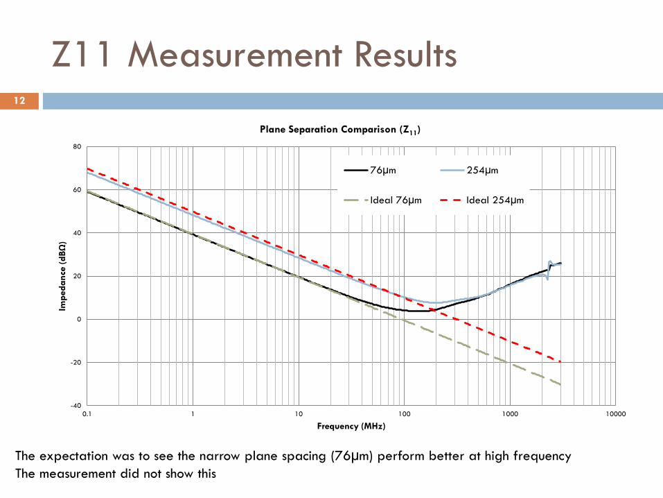
Z11 Measurement Results12
The expectation was to see the narrow plane spacing (76µm) perform better at high frequency
The measurement did not show this
-40
-20
0
20
40
60
80
0.1 1 10 100 1000 10000
Imp
edan
ce (
dBΩ
)
Frequency (MHz)
Plane Separation Comparison (Z11)
76µm 254µm
Ideal 76µm Ideal 254µm

Single port measurement and
simulation13
-50
-40
-30
-20
-10
0
10
20
30
40
50
10 100 1000
Z1
1 (
dB
)
Frequency (MHz)
Single Port Impedance vs. Connector Height
Simulation Data
2mm height
1.1mm height
0.2mm height
• Simulations were
performed using the
Finite Integration
Technique
• It was discovered that
the high frequency
impedance was
dependent upon the
height of the coax
connector
• 0.2mm height was
represented by a port
existing between PCB
planes

New Measurement Methodology14
Network Analyzer
Port 1
PCB
Port 2
To port 1
To port 2
Plane 1
Plane 2

S21 Test Setup
50ΩSource
50ΩLoad
Distributed
Embedded
Capacitance
Path 1 Path 2
15

EM Simulation16
Technique:
Full Wave 3D Solver
Finite Integration Method

EM Simulation vs. Measurement17

6” x 2” PCB with
3 Mils Plane Separation (FR4 Core)
Source and 50 ΩLoad at Center
18

-70
-60
-50
-40
-30
-20
-10
0
10
1 10 100 1000 10000
Rela
tive Im
pedance
(dBΩ
)
Frequency (MHz)
Calculated vs. Simulated Plane Pair Impedance
Z Simulated
Z Calculated
Embedded capacitance works as a parallel plate
capacitor at low frequencies but at higher frequencies
other factors become dominant
19
Impedance of

Capacitors
Energy is stored in a capacitor as an electric field
In the following field plots
A strong electric field indicates the applied energy was
used to charge the planes
A weak electric field indicates that embedded
capacitance was utilized thus generating a magnetic
field.

Electric Field at 10 MHz
-70
-60
-50
-40
-30
-20
-10
0
10
1 10 100 1000 10000
Z Simulated
Z Calculated

Electric Field at 100 MHz
-70
-60
-50
-40
-30
-20
-10
0
10
1 10 100 1000 10000
Z Simulated
Z Calculated

Electric Field at 170 MHz-70
-60
-50
-40
-30
-20
-10
0
10
1 10 100 1000 10000
Z Simulated
Z Calculated

Electric Field at 250 MHz
-70
-60
-50
-40
-30
-20
-10
0
10
1 10 100 1000 10000
Z Simulated
Z Calculated

Electric Field at 800 MHz
-70
-60
-50
-40
-30
-20
-10
0
10
1 10 100 1000 10000
Z Simulated
Z Calculated
Scale
Changed
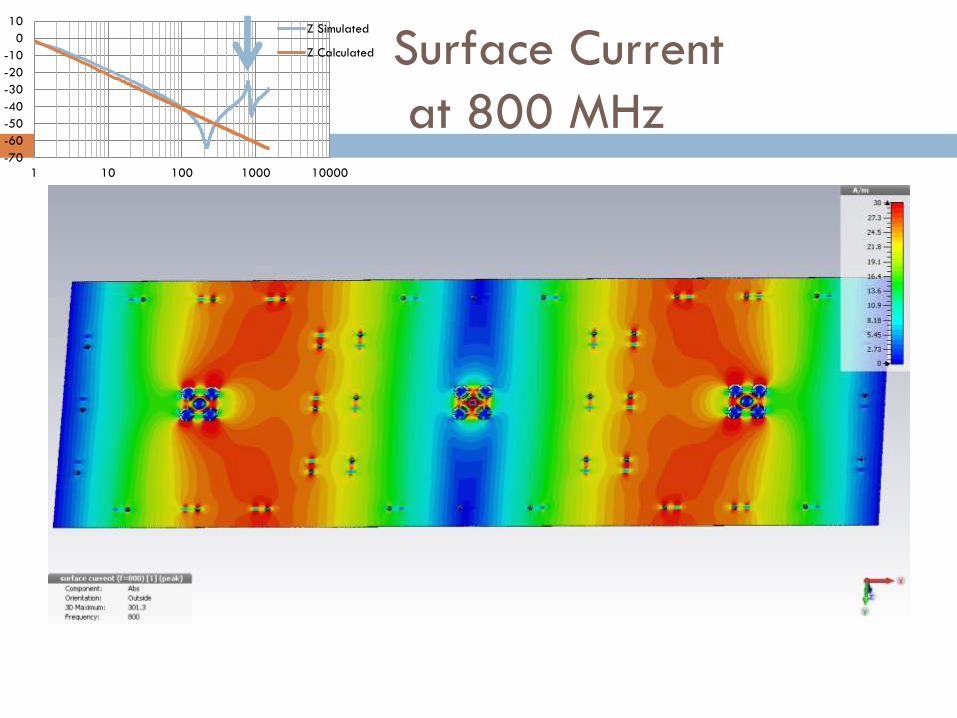
Surface Current
at 800 MHz-70
-60
-50
-40
-30
-20
-10
0
10
1 10 100 1000 10000
Z Simulated
Z Calculated
Scale
Changed

Concept of Embedded Capacitance
Below 100 MHz, PCB capacitance is utilized
throughout the entire PCB and behaves as an ideal
parallel plate capacitor
Above 100 MHz other factors cause impedance to
increase making the PCB not an ideal parallel plate
capacitor
PCBs of various dimensions with
discrete capacitorsDemonstration

Example
4x4 inch PCB with 2 adjacent
plane layers and capacitor pads
Will compare
- 3 mil plane spacing
- 30 mil plane spacing
Each comparison will involve
capacitors located
-1 inch away from the source
- 2 inches away from the source

-80
-70
-60
-50
-40
-30
-20
-10
0
1 10 100 1000
S21 (
dB)
Frequency (MHz)
Decoupling Capacitor Placement
4x4 3 mil close
4x4 3 mil far
4x4 30 mil close
4x4 30 mil far

Capacitor Location
As plane distance decreases, distance between the
capacitors and the excitation source (or load)
becomes less important

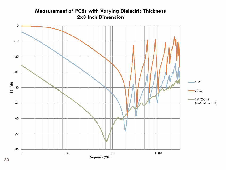
PCBs of various dielectric thicknesses
and the same dimensions32
-80
-70
-60
-50
-40
-30
-20
-10
0
1 10 100 1000
S21 (
dB)
Frequency (MHz)
Measurement of PCBs with Varying Dielectric Thickness2x8 Inch Dimension
3 Mil
30 Mil
3M C0614(0.55 mil not FR4)
33

Dielectric Thickness
Closer plane spacing results in lower plane
impedance at low frequencies as well as high
frequencies
Lower Q factor is also achieved by closer plane
spacing
34

PCBs of various dimensions and the
same dielectric thickness35

-80
-70
-60
-50
-40
-30
-20
-10
0
1 10 100 1000
S21 (
dB)
Frequency (MHz)
Measurement of PCBs with Varying Dimensions3 mil Dielectric Thickness
2x2"
2x6"
36
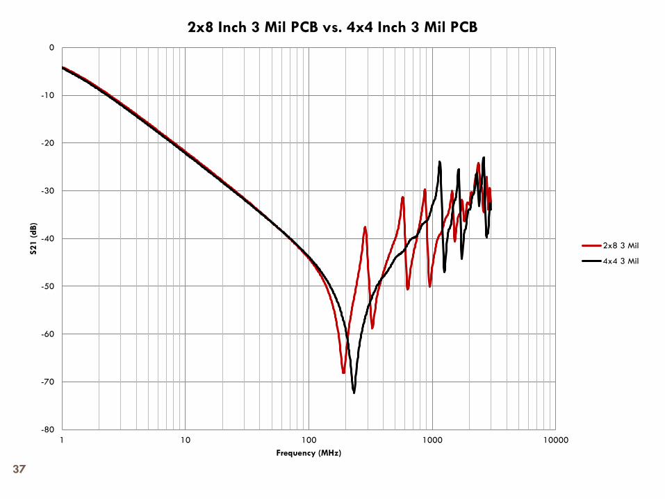
37
-80
-70
-60
-50
-40
-30
-20
-10
0
1 10 100 1000 10000
S21 (
dB)
Frequency (MHz)
2x8 Inch 3 Mil PCB vs. 4x4 Inch 3 Mil PCB
2x8 3 Mil
4x4 3 Mil

Plane Area
Increasing PCB size causes lower impedance at low
frequencies, but does not affect impedance at high
frequencies
PCBs with identical plane area but different length
and width dimensions can have different
impedances at high frequency
38

Impact of Dielectric Material39

Ceramic Core Dielectric <3 mil40
Simulation results
-90
-80
-70
-60
-50
-40
-30
-20
-10
0
1 10 100 1000
S2
1 (
dB
)
Frequency (MHz)
FR4 Core vs Ceramic Core Material
12µm Plane Separation
Ceramic Core FR4 Core

Dielectric Material41
Higher permittivity materials definitely have their
advantages at lower frequency
At higher frequency (in this case around 200MHz
and up) the core material does not provide lower
impedance
Remember: closer plane spacing DOES impact high
frequency impedance
New materials can make it easier (cost effective) to
manufacture PCBs with very close layers

PCBs of various dimensions with
discrete capacitors42

12 x 0.1µF capacitors added43

-90
-80
-70
-60
-50
-40
-30
-20
-10
0
1 10 100
S21 (
dB)
Frequency (MHz)
Measurements of PCBs with and without Capacitors2x8" 3 mil Dielectric
12x0.1µF Caps
No Caps
44

-90
-80
-70
-60
-50
-40
-30
-20
-10
0
1 10 100
S21
(dB)
Frequency (MHz)
Measurements of PCBs with and without Capacitors2x8" with 3 mil Dielectric & 3M Dielectric
12x0.1µF Caps
No Caps
No Caps 3 M Material
45

The Concept
Discrete chip decoupling capacitors
provide low impedance at low
frequencies (<100 MHz) but not at
higher frequencies due to ESL
Embedded capacitance provides low
impedance at high frequencies but
typically do not perform as well as
discrete capacitors in their usable
range
Why not use
both?
46

47
-90
-80
-70
-60
-50
-40
-30
-20
-10
0
1 10 100 1000
S21 (
dB)
Frequency (MHz)
6x23cm PCBs with and without Capacitors76µm Dielectric
12x0.1µF Caps No Caps
PCB DominatesCapacitors Dominate

Radiated Emissions caused by plane
resonance48

Radiated Emissions Setup
Network
AnalyzerPort 1 Port 2
PCB
Antenna
Load
2 m longWires
Anechoic Chamber
1m
Metal Table

-80
-60
-40
-20
0
20
40
60
80
0 100 200 300 400 500 600 700 800 900 1000
S21 (
dB)
and E
lect
ric
Fie
ld (
dBµ
V/m
)
Frequency (MHz)
Comparison Between Decoupling Analysis and Radiated Emissions
Impedance
Measurement
Radiated
Emissions
Measurement
50

Radiated Emissions vs. PCB Impedance51
The measurement shows correlation between plane
resonance and emissions
Inadequate PDN impedance may cause excessive
emissions
PCB geometry is an important factor in emissions
results

Changing PCB resonance frequency52

-90
-80
-70
-60
-50
-40
-30
-20
-10
0
1 10 100 1000
S21 (
dB)
Frequency (MHz)
Measurements of PCBs with and without Capacitors2x8" 3 mil Dielectric
12x0.1µF Caps
No Caps
133 MHz
53
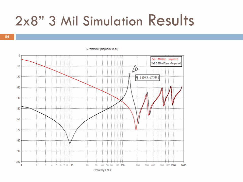
2x8” 3 Mil Simulation Results54

Equivalent Circuit
Short Circuit
at High
Frequency
Still a Capacitor
at High
Frequency
LC Resonance
55

0.1 µF vs. 1 µF Capacitor Values56

Discrete Capacitors and Embedded
Capacitance
Discrete capacitors and embedded capacitance can
interact causing a parallel resonance raising PCB
impedance at some frequencies even as low as 130
MHz for a 2x8” PCB
This resonance is caused by the embedded
capacitance and the ESL of the capacitor
The value of the capacitor is not important
57

Manipulation of the first parallel
resonance58

#1 Change
Plane Spacing59
-90
-80
-70
-60
-50
-40
-30
-20
-10
0
1 10 100 1000
S21 (
dB)
Frequency (MHz)
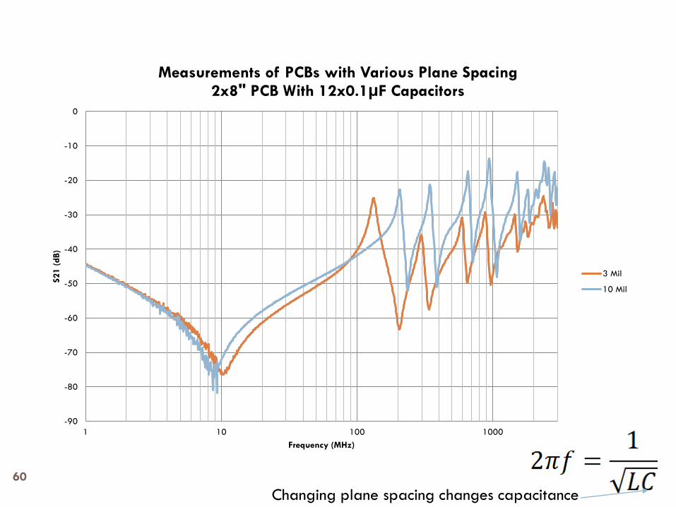
Measurements of PCBs with Various Plane Spacing2x8" PCB With 12x0.1µF Capacitors
3 Mil
10 Mil
60
Changing plane spacing changes capacitance

#2 – Change Number of capacitors61

-90
-80
-70
-60
-50
-40
-30
-20
-10
0
1 10 100 1000
S21 (
dB)
Frequency (MHz)
Measurements of PCBs with Various Number of Capacitors2x8" PCB With 3 Mil Plane Spacing
12x0.1µF Caps
4x0.1µF Caps
62
Changing the number of capacitors changes inductance

#3 Change PCB Dimensions63

-90
-80
-70
-60
-50
-40
-30
-20
-10
0
1 10 100 1000
S21 (
dB)
Frequency (MHz)
Measurement of PCBs with Varying Dimensions3 mil Dielectric Thickness with 12x0.1µF Capacitors
2x8"
2x6"
2x2"
64
PCB
dimensions
affect
capacitance

One Plane Split65

-90
-80
-70
-60
-50
-40
-30
-20
-10
0
1 10 100 1000
S21 (
dB)
Frequency (MHz)
Measurement of PCBs with Varying Dimensions3 mil Dielectric Thickness with 12x0.1µF Capacitors
2x8" Solid
Split Plane2x2" Section
2x2"
66
Splitting the plane will decrease the plane area causing a lower capacitance value

#4 - High ESR Capacitors
0603 Size capacitors made by TDK
Center terminal is not connected to anything
Contains up to 1.2 Ohms of series resistance
More expensive than standard capacitors but
benefit can be seen by replacing some standard
capacitors with high ESR capacitors
67

-90
-80
-70
-60
-50
-40
-30
-20
-10
0
1 10 100 1000
Axis
Title
Axis Title
Measurement of PCBs with Varying Capacitor Types2x8" 3 mil Dielectric Thickness
12x0.1µF
8x0.1µF &4xHigh ESR
68
Resistance in series with the capacitor will create loss at the resonant frequency

Parallel Resonance due to Embedded
Capacitance
Further plane spacing = higher frequency
resonance
More capacitors = higher frequency resonance
Smaller planes = higher frequency resonance
More Series Resistance = less resonance
Is a higher frequency resonance better
than a lower frequency resonance?
….. It depends!
69

Summary70
Plane impedance can be determined using EM simulation and measuring equipment but plane connections may cause error
PCB Power/Ground Plane Separation
Below resonant frequency, the PCB planes behave as a parallel plate capacitor and the capacitance can be easily calculated
Above resonant frequency, plane impedance is more complicated and it depends on several factors including PCB geometry
Dielectric Material
Higher permittivity materials cause higher capacitance below the PCB resonance which can be useful in PDN design
Higher permittivity materials do not make a significant difference in PDN impedance at high frequency but the close plane spacing which generally accompanies high permittivity materials make a great difference
Adding Discrete capacitors
PCB embedded capacitance for most devices still can’t provide low impedance PDN compared to discrete capacitor components on PCBs
Using embedded PCB capacitance along with discrete capacitors can be a good solutionbut will cause a resonance at a frequency depending on the number of capacitors and the amount of PCB capacitance.
Related Documents