E4000 MULTI‐STANDARD CMOS TERRESTRIAL RF TUNER E4000 Datasheet 4v0 Copyright ©2010 Elonics Ltd Document Number :S‐E4000‐DS001 www.elonics.com KEY FEATURES Support for Multiple Broadcast Standards o NorDig 2.0 o MBRAI 2.0 Scalable Power Consumption o 118mW Typical Operation o 15mW in DVB‐H Mode o <60uW Power Down 1.5V Analogue and Digital Supply Operation Variable Gain Low Noise Amplifier (LNA) o Autonomous Automatic Gain Control with RSSI o <4dB Receiver Noise Figure o 64MHz to 1700MHz Input Frequency Range Flexible IF Amplifier and Channel Filter o Programmable Channel Bandwidth o Digital IF Gain Control Flexible Clocking Modes o Master or Slave Mode Device o 16MHz – 32MHz Input Frequency Range o Programmable Output Clock Frequency Range o CMOS or custom low power LVDS Output Levels Fractional‐N Synthesiser with Fully Integrated VCO and Loop Filter I 2 C Compatible Control Bus o 3.3V Tolerant Interface o 4 Addresses 32‐Pin QFN Package o 5 x 5 x 0.9 mm Body Size o Pb‐Free o RoHS Compliant APPLICATIONS TV Enabled Cell Phones Portable Multimedia Players PC and PC Peripherals IPTV Set Top Boxes DESCRIPTION The E4000 is a highly integrated multi‐band RF tuner IC implemented in CMOS, ideal for digital TV and radio broadcast receiver solutions. The digitally programmable multi‐band tuner architecture allows the user to re‐configure the RF front end for different broadcast standards. DVB‐T (174‐240MHz, 470‐858MHz) CMMB Terrestrial (470‐858MHz) D‐TMB (174‐240MHz, 1452‐1492MHz) ISDB‐T (470 – 862MHz) DVB‐H (470 – 858MHz, 1672‐1678MHz) T‐DMB (174 – 240MHz, 1452 – 1492MHz) DAB/DAB+ (174 – 240MHz, 1452 – 1492MHz) GPS L1 band (1575MHz) – (with additional LNA) FM radio (64 – 108MHz) It is designed to interface directly to a digital demodulator, and contains a fully integrated LNA, programmable RF filter, and RF mixers providing superior real world performance. At the heart of the E4000 is Elonics innovative DigitalTune™ architecture, which allows the user to adjust the performance of the tuner for optimum linearity or noise figure according to the signal conditions. It enables manufacturers to significantly improve reception quality, whilst supporting multiple broadcast standards. The E4000 contains a single input LNA with RF filter, whose centre frequency can be programmed over the complete frequency range from 64MHz to 1700MHz. This greatly simplifies antenna management especially for applications that require support for more than one broadcast standard. NIM and half NIM modules

Welcome message from author
This document is posted to help you gain knowledge. Please leave a comment to let me know what you think about it! Share it to your friends and learn new things together.
Transcript

E4000MULTI‐STANDARD CMOS TERRESTRIAL RF TUNER
E4000 Datasheet 4v0 Copyright ©2010 Elonics Ltd Document Number :S‐E4000‐DS001 www.elonics.com
KEY FEATURES
Support for Multiple Broadcast Standards o NorDig 2.0 o MBRAI 2.0
Scalable Power Consumption o 118mW Typical Operation o 15mW in DVB‐H Mode o <60uW Power Down
1.5V Analogue and Digital Supply Operation
Variable Gain Low Noise Amplifier (LNA) o Autonomous Automatic Gain Control
with RSSI o <4dB Receiver Noise Figure o 64MHz to 1700MHz Input Frequency
Range
Flexible IF Amplifier and Channel Filter o Programmable Channel Bandwidth o Digital IF Gain Control
Flexible Clocking Modes o Master or Slave Mode Device o 16MHz – 32MHz Input Frequency
Range o Programmable Output Clock
Frequency Range o CMOS or custom low power LVDS
Output Levels
Fractional‐N Synthesiser with Fully Integrated VCO and Loop Filter
I2C Compatible Control Bus o 3.3V Tolerant Interface o 4 Addresses
32‐Pin QFN Package o 5 x 5 x 0.9 mm Body Size o Pb‐Free o RoHS Compliant
APPLICATIONS
TV Enabled Cell Phones
Portable Multimedia Players
PC and PC Peripherals
IPTV
Set Top Boxes
DESCRIPTION
The E4000 is a highly integrated multi‐band RF tuner IC implemented in CMOS, ideal for digital TV and radio broadcast receiver solutions. The digitally programmable multi‐band tuner architecture allows the user to re‐configure the RF front end for different broadcast standards.
DVB‐T (174‐240MHz, 470‐858MHz)
CMMB Terrestrial (470‐858MHz)
D‐TMB (174‐240MHz, 1452‐1492MHz)
ISDB‐T (470 – 862MHz)
DVB‐H (470 – 858MHz, 1672‐1678MHz)
T‐DMB (174 – 240MHz, 1452 – 1492MHz)
DAB/DAB+ (174 – 240MHz, 1452 – 1492MHz)
GPS L1 band (1575MHz) – (with additional LNA)
FM radio (64 – 108MHz)
It is designed to interface directly to a digital demodulator, and contains a fully integrated LNA, programmable RF filter, and RF mixers providing superior real world performance.
At the heart of the E4000 is Elonics innovative DigitalTune™ architecture, which allows the user to adjust the performance of the tuner for optimum linearity or noise figure according to the signal conditions. It enables manufacturers to significantly improve reception quality, whilst supporting multiple broadcast standards.
The E4000 contains a single input LNA with RF filter, whose centre frequency can be programmed over the complete frequency range from 64MHz to 1700MHz. This greatly simplifies antenna management especially for applications that require support for more than one broadcast standard.
NIM and half NIM modules
E4000
E4000 Datasheet 4v0 S‐E4000‐DS001 August 2010
UNCONTROLLED WHEN PRINTED UNLESS STAMPED OTHERWISECopyright ©2010 Elonics Ltd
Page 2
TABLE OF CONTENTS
KEY FEATURES ‐‐‐‐‐‐‐‐‐‐‐‐‐‐‐‐‐‐‐‐‐‐‐‐‐‐‐‐‐‐‐‐‐‐‐‐‐‐‐‐‐‐‐‐‐‐‐‐‐‐‐‐‐‐‐‐‐‐‐‐‐‐‐‐‐‐‐‐‐‐‐‐‐‐‐‐‐‐‐‐‐‐‐‐‐‐‐‐‐‐‐‐‐‐‐‐‐‐‐‐‐‐‐‐‐‐‐‐‐ 1 APPLICATIONS ‐‐‐‐‐‐‐‐‐‐‐‐‐‐‐‐‐‐‐‐‐‐‐‐‐‐‐‐‐‐‐‐‐‐‐‐‐‐‐‐‐‐‐‐‐‐‐‐‐‐‐‐‐‐‐‐‐‐‐‐‐‐‐‐‐‐‐‐‐‐‐‐‐‐‐‐‐‐‐‐‐‐‐‐‐‐‐‐‐‐‐‐‐‐‐‐‐‐‐‐‐‐‐‐‐‐‐‐‐ 1 DESCRIPTION ‐‐‐‐‐‐‐‐‐‐‐‐‐‐‐‐‐‐‐‐‐‐‐‐‐‐‐‐‐‐‐‐‐‐‐‐‐‐‐‐‐‐‐‐‐‐‐‐‐‐‐‐‐‐‐‐‐‐‐‐‐‐‐‐‐‐‐‐‐‐‐‐‐‐‐‐‐‐‐‐‐‐‐‐‐‐‐‐‐‐‐‐‐‐‐‐‐‐‐‐‐‐‐‐‐‐‐‐‐‐‐ 1 TABLE OF CONTENTS ‐‐‐‐‐‐‐‐‐‐‐‐‐‐‐‐‐‐‐‐‐‐‐‐‐‐‐‐‐‐‐‐‐‐‐‐‐‐‐‐‐‐‐‐‐‐‐‐‐‐‐‐‐‐‐‐‐‐‐‐‐‐‐‐‐‐‐‐‐‐‐‐‐‐‐‐‐‐‐‐‐‐‐‐‐‐‐‐‐‐‐‐‐‐‐‐‐‐‐‐‐ 2 ORDERING INFORMATION ‐‐‐‐‐‐‐‐‐‐‐‐‐‐‐‐‐‐‐‐‐‐‐‐‐‐‐‐‐‐‐‐‐‐‐‐‐‐‐‐‐‐‐‐‐‐‐‐‐‐‐‐‐‐‐‐‐‐‐‐‐‐‐‐‐‐‐‐‐‐‐‐‐‐‐‐‐‐‐‐‐‐‐‐‐‐‐‐‐‐‐‐‐ 5 PACKAGE MARKING DIAGRAM ‐‐‐‐‐‐‐‐‐‐‐‐‐‐‐‐‐‐‐‐‐‐‐‐‐‐‐‐‐‐‐‐‐‐‐‐‐‐‐‐‐‐‐‐‐‐‐‐‐‐‐‐‐‐‐‐‐‐‐‐‐‐‐‐‐‐‐‐‐‐‐‐‐‐‐‐‐‐‐‐‐‐‐‐‐‐‐ 5 PIN FUNCTIONS ‐‐‐‐‐‐‐‐‐‐‐‐‐‐‐‐‐‐‐‐‐‐‐‐‐‐‐‐‐‐‐‐‐‐‐‐‐‐‐‐‐‐‐‐‐‐‐‐‐‐‐‐‐‐‐‐‐‐‐‐‐‐‐‐‐‐‐‐‐‐‐‐‐‐‐‐‐‐‐‐‐‐‐‐‐‐‐‐‐‐‐ ‐‐‐‐‐‐‐‐‐‐‐‐‐‐‐ 7 ABSOLUTE MAXIMUM RATINGS ‐‐‐‐‐‐‐‐‐‐‐‐‐‐‐‐‐‐‐‐‐‐‐‐‐‐‐‐‐‐‐‐‐‐‐‐‐‐‐‐‐‐‐‐‐‐‐‐‐‐‐‐‐‐‐‐‐‐‐‐‐‐‐‐‐ ‐‐‐ ‐‐‐‐‐‐‐‐‐‐‐‐‐‐ 8 MOISTURE SENSITIVITY ‐‐‐‐‐‐‐‐‐‐‐‐‐‐‐‐‐‐‐‐‐‐‐‐‐‐‐‐‐‐‐‐‐‐‐‐‐‐‐‐‐‐‐‐‐‐‐‐‐‐‐‐‐‐‐‐‐‐‐‐‐‐‐‐‐‐‐‐‐‐‐‐‐‐‐ ‐‐‐‐‐‐‐‐‐‐‐‐‐‐‐‐‐‐‐‐‐ 8 RECOMMENDED OPERATING CONDITIONS ‐‐‐‐‐‐‐‐‐‐‐‐‐‐‐‐‐‐‐‐‐‐‐‐‐‐‐‐‐‐‐‐‐‐‐‐‐‐‐‐‐‐‐ ‐‐‐‐‐‐‐‐‐‐‐‐‐‐‐‐‐‐‐‐‐‐‐‐ 8 DC ELECTRICAL CHARACTERISTICS ‐‐‐‐‐‐‐‐‐‐‐‐‐‐‐‐‐‐‐‐‐‐‐‐‐‐‐‐‐‐‐‐‐‐‐‐‐‐‐‐‐‐‐‐‐‐‐‐‐‐‐‐‐‐‐‐‐‐‐‐‐‐‐‐‐‐‐‐‐‐‐‐‐‐‐‐‐‐‐‐‐‐‐ 9 AC ELECTRICAL CHARACTERISTICS ‐‐‐‐‐‐‐‐‐‐‐‐‐‐‐‐‐‐‐‐‐‐‐‐‐‐‐‐‐‐‐‐‐‐‐‐‐‐‐‐‐‐‐‐‐‐‐‐‐ ‐ ‐‐‐‐‐‐‐‐‐‐‐‐‐‐‐‐‐‐‐‐‐‐‐‐‐‐‐ 11 POWER CONSUMPTION ‐‐‐‐‐‐‐‐‐‐‐‐‐‐‐‐‐‐‐‐‐‐‐‐‐‐‐‐‐‐‐‐‐‐‐‐‐‐‐‐‐‐‐‐‐‐‐‐‐‐‐‐‐‐‐‐‐‐‐ ‐‐ ‐‐‐‐‐‐‐‐‐‐‐‐ ‐‐‐‐‐‐‐‐‐‐‐‐‐‐‐‐ 13 TIMING CHARACTERISTICS ‐‐‐‐‐‐‐‐‐‐‐‐‐‐‐‐‐‐‐‐‐‐‐‐‐‐‐‐‐‐‐‐‐‐‐‐‐‐‐‐‐‐‐‐‐‐‐‐‐‐‐ ‐‐ ‐‐ ‐‐‐‐‐‐‐‐‐‐‐ ‐‐‐‐‐ ‐‐‐‐‐‐‐‐‐‐‐‐‐‐ 14 TYPICAL CHARACTERISTICS ‐‐‐‐‐‐‐‐‐‐‐‐‐‐‐‐‐‐‐‐‐‐‐‐‐‐‐‐‐‐‐‐‐‐‐‐‐‐‐‐‐‐‐‐‐‐‐‐ ‐‐ ‐‐‐‐‐‐‐‐‐‐ ‐‐ ‐‐‐‐ ‐‐‐‐‐‐‐‐‐‐‐‐‐‐‐‐‐‐‐ 15 REGISTER MAP ‐‐‐‐‐‐‐‐‐‐‐‐‐‐‐‐‐‐‐‐‐‐‐‐‐‐‐‐‐‐‐‐‐‐‐‐‐‐‐‐‐‐‐‐‐‐‐‐‐‐‐‐‐‐‐‐‐‐‐‐‐ ‐‐‐ ‐‐‐‐‐‐‐‐‐‐‐‐‐‐‐‐ ‐‐‐‐‐‐‐‐‐‐‐‐‐‐‐‐‐‐‐‐‐‐‐‐ 17 DEVICE DESCRIPTION ‐‐‐‐‐‐‐‐‐‐‐‐‐‐‐‐‐‐‐‐‐‐‐‐‐‐‐‐‐‐‐‐‐‐‐‐‐‐‐‐‐‐‐‐‐‐ ‐ ‐‐‐‐‐‐‐‐‐‐‐‐‐‐‐‐‐‐‐‐‐‐‐‐‐‐‐‐‐‐‐‐‐‐‐‐‐‐‐‐‐‐‐‐‐‐‐‐‐ 23 1.1 Two Wire, I2C Interface ‐‐‐‐‐‐‐‐‐‐‐‐‐‐‐‐‐‐‐‐‐‐‐‐‐‐‐‐‐‐‐‐‐‐‐‐‐‐‐‐‐‐‐‐ ‐‐ ‐ ‐‐‐‐‐‐‐‐‐‐‐‐‐‐‐ ‐ ‐‐‐‐‐‐‐‐‐‐‐‐‐‐‐‐‐‐‐‐‐‐‐‐‐‐‐‐‐‐‐‐‐‐‐‐‐‐‐ 23 1.2 Serial Interface Protocol ‐‐‐‐‐‐‐‐‐‐‐‐‐‐‐‐‐‐‐‐‐‐‐‐‐‐‐‐‐‐‐‐‐‐‐‐‐‐‐‐‐ ‐‐‐ ‐‐‐‐‐‐‐‐‐‐‐‐‐ ‐ ‐‐ ‐‐‐‐‐‐‐‐‐‐‐‐‐‐‐‐‐‐‐‐‐‐‐‐‐‐‐‐‐‐‐‐‐‐‐‐‐‐‐‐‐‐‐ 23 1.3 Frequency Synthesiser ‐‐‐‐‐‐‐‐‐‐‐‐‐‐‐‐‐‐‐‐‐‐‐‐‐‐‐‐‐‐‐‐‐‐‐‐‐‐‐ ‐‐‐ ‐‐‐‐‐‐‐‐‐‐‐‐‐‐‐‐ ‐‐‐‐‐‐‐‐‐‐‐‐‐‐‐‐‐‐‐‐‐‐‐‐‐‐‐‐‐‐‐‐‐‐‐‐‐‐‐‐‐‐‐‐‐‐‐‐‐‐ 25 1.4 PLL Feedback divider (/Z) ‐‐‐‐‐‐‐‐‐‐‐‐‐‐‐‐‐‐‐‐‐‐‐‐‐‐‐‐‐‐ ‐‐‐‐‐ ‐‐‐‐‐‐‐‐‐‐‐‐‐‐‐ ‐ ‐‐‐‐‐‐‐‐‐‐‐‐‐‐‐‐‐‐‐‐‐‐‐‐‐‐‐‐‐‐‐‐‐‐‐‐‐‐‐‐‐‐‐‐‐‐‐‐‐‐ 26 1.5 ‘X’, Sigma delta setup ‐‐‐‐‐‐‐‐‐‐‐‐‐‐‐‐‐‐‐‐‐‐‐‐‐‐ ‐‐‐‐‐‐‐‐‐‐‐‐‐‐‐‐‐‐‐‐‐‐‐‐‐‐ ‐‐‐ ‐‐‐‐‐‐‐‐‐‐‐‐‐‐‐‐‐‐‐‐‐‐‐‐‐‐‐‐‐‐‐‐‐‐‐‐‐‐‐‐‐‐‐‐‐‐‐‐‐‐‐‐‐ 26 1.6 R – VCO output divider ‐‐‐‐‐‐‐‐‐‐‐‐‐‐‐‐‐‐‐‐‐‐‐‐‐‐‐ ‐‐‐‐‐‐‐‐‐‐‐‐‐‐‐‐ ‐‐‐‐‐ ‐‐‐‐‐‐‐‐‐‐‐‐‐‐‐‐‐‐‐‐‐‐‐‐‐‐‐‐‐‐‐‐‐‐‐‐‐‐‐‐‐‐‐‐‐‐‐‐‐‐‐‐‐‐‐‐‐ 26 1.7 Three phase mixing ‐‐‐‐‐‐‐‐‐‐‐‐‐‐‐‐‐‐‐‐‐ ‐‐‐‐‐ ‐‐ ‐‐‐‐‐‐‐‐‐‐‐ ‐‐‐‐‐ ‐‐‐‐‐‐‐‐‐‐‐‐‐‐‐‐‐‐‐‐‐‐‐‐‐‐‐‐‐‐‐‐‐‐‐‐‐‐‐‐‐‐‐‐‐‐‐‐‐‐‐‐‐‐‐‐‐‐‐‐‐‐‐‐‐ 26 1.8 Example Frequency synthesizer configuration ‐‐‐‐‐‐‐ ‐‐‐‐ ‐‐‐‐‐‐‐‐‐‐‐‐‐‐‐‐‐‐‐‐‐‐‐‐‐‐‐‐‐‐‐‐‐‐‐‐‐‐‐‐‐‐‐‐‐‐‐‐‐‐‐‐‐‐‐‐‐‐‐‐‐‐‐‐‐ 27 1.9 VCO Calibration ‐‐‐‐‐‐‐‐‐‐‐‐‐‐‐‐‐‐‐‐‐‐‐‐‐‐‐ ‐‐‐‐‐‐‐‐‐‐‐‐‐‐‐‐‐‐‐‐‐‐ ‐‐‐‐‐‐‐‐‐‐‐‐‐‐‐‐‐‐‐‐‐‐‐‐‐‐‐‐‐‐‐‐‐‐‐‐‐‐‐‐‐‐‐‐‐‐‐‐‐‐‐‐‐‐‐‐‐‐‐‐‐‐‐‐‐‐‐‐‐ 27 1.10 E4000 Signal Path ‐‐‐‐‐‐‐‐‐‐‐‐‐‐ ‐‐‐‐‐‐‐‐‐‐‐‐‐‐‐‐‐‐ ‐‐ ‐‐‐‐ ‐‐‐‐‐‐‐‐‐‐‐‐‐‐‐‐‐‐‐‐‐‐‐‐‐‐‐‐‐‐‐‐‐‐‐‐‐‐‐‐‐‐‐‐‐‐‐‐‐‐‐‐‐‐‐‐‐‐‐‐‐‐‐‐‐‐‐‐‐‐‐‐‐‐ 28 1.11 Frequency Band Selection ‐‐ ‐‐ ‐‐‐‐‐‐‐‐‐‐‐‐‐‐‐‐ ‐‐‐‐‐‐‐‐‐‐‐‐‐‐‐‐‐‐‐‐‐‐‐‐‐‐‐‐‐‐‐‐‐‐‐‐‐‐‐‐‐‐‐‐‐‐‐‐‐‐‐‐‐‐‐‐‐‐‐‐‐‐‐‐‐‐‐‐‐‐‐‐‐‐‐‐‐‐‐‐‐ 29 1.12 Gain Control ‐‐‐‐‐‐‐‐‐‐‐‐‐‐‐‐ ‐‐ ‐‐ ‐‐‐‐‐‐‐‐‐‐‐‐ ‐‐‐‐‐‐‐‐‐‐‐‐‐‐‐‐‐‐‐‐‐‐‐‐‐‐‐‐‐‐‐‐‐‐‐‐‐‐‐‐‐‐‐‐‐‐‐‐‐‐‐‐‐‐‐‐‐‐‐‐‐‐‐‐‐‐‐‐‐‐‐‐‐‐‐‐‐‐‐‐‐‐‐‐‐‐‐ 30 1.13 LNA Gain Control ‐‐‐‐ ‐‐‐ ‐‐‐‐‐‐‐‐‐‐‐‐ ‐‐ ‐‐‐‐‐‐‐‐‐‐‐‐‐‐‐‐‐‐‐‐‐‐‐‐‐‐‐‐‐‐‐‐‐‐‐‐‐‐‐‐‐‐‐‐‐‐‐‐‐‐‐‐‐‐‐‐‐‐‐‐‐‐‐‐‐‐‐‐‐‐‐‐‐‐‐‐‐‐‐‐‐‐‐‐‐‐‐‐ 30
1.13.1 LNA ‐ Serial Interface Gain Contro ‐‐‐‐‐‐‐‐‐‐‐‐‐‐‐‐‐‐‐‐‐‐‐‐‐‐‐‐‐‐‐‐‐‐‐‐‐‐‐‐‐‐‐‐‐‐‐‐‐‐‐‐‐‐‐‐‐‐‐‐‐‐‐‐‐‐‐‐‐‐‐‐‐‐‐‐‐‐‐‐‐‐‐‐‐‐‐‐‐‐ 31 1.13.2 LNA ‘digital’ PWM gain control ‐‐‐‐‐‐‐‐‐‐‐‐‐‐‐‐‐‐‐‐‐‐‐‐‐‐‐‐‐‐‐‐‐‐‐‐‐‐‐‐‐‐‐‐‐‐‐‐‐‐‐‐‐‐‐‐‐‐‐‐‐‐‐‐‐‐‐‐‐‐‐‐‐‐‐‐‐‐‐‐‐‐‐‐‐‐‐‐‐‐‐‐‐‐ 32 1.13.3 LNA Autonomous Gain Control ‐‐‐‐‐‐‐‐‐‐‐‐‐‐‐‐‐‐‐‐‐‐‐‐‐‐‐‐‐‐‐‐‐‐‐‐‐‐‐‐‐‐‐‐‐‐‐‐‐‐‐‐‐‐‐‐‐‐‐‐‐‐‐‐‐‐‐‐‐‐‐‐‐‐‐‐‐‐‐‐‐‐‐‐‐‐‐‐‐‐‐‐‐‐ 33 1.13.4 LNA Supervisor Gain Control ‐‐‐‐‐‐‐‐‐‐‐‐‐‐‐‐‐‐‐‐‐‐‐‐‐‐‐‐‐‐‐‐‐‐‐‐‐‐‐‐‐‐‐‐‐‐‐‐‐‐‐‐‐‐‐‐‐‐‐‐‐‐‐‐‐‐‐‐‐‐‐‐‐‐‐‐‐‐‐‐‐‐‐‐‐‐‐‐‐‐‐‐‐‐‐‐‐ 33
1.14 Received Signal Strength Indicator (RSSI) ‐‐‐‐‐‐‐‐‐‐‐‐‐‐‐‐‐‐‐‐‐‐‐‐‐‐‐‐‐‐‐‐‐‐‐‐‐‐‐‐‐‐‐‐‐‐‐‐‐‐‐‐‐‐‐‐‐‐‐‐‐‐‐‐‐‐‐‐‐‐‐‐‐‐‐‐‐‐‐‐‐‐‐‐‐‐‐ 34 1.15 Mixer Gain Control ‐‐‐‐‐‐‐‐‐‐‐‐‐‐‐‐‐‐‐‐‐‐‐‐‐‐‐‐‐‐‐‐‐‐‐‐‐‐‐‐‐‐‐‐‐‐‐‐‐‐‐‐‐‐‐‐‐‐‐‐‐‐‐‐‐‐‐‐‐‐‐‐‐‐‐‐‐‐‐‐‐‐‐‐‐‐‐‐‐‐‐‐‐‐‐‐‐‐‐‐‐‐‐‐‐‐‐‐‐‐‐‐‐‐‐ 34
1 15.1 Mixer Gain – Serial Interface Control ‐‐‐‐‐‐‐‐‐‐‐‐‐‐‐‐‐‐‐‐‐‐‐‐‐‐‐‐‐‐‐‐‐‐‐‐‐‐‐‐‐‐‐‐‐‐‐‐‐‐‐‐‐‐‐‐‐‐‐‐‐‐‐‐‐‐‐‐‐‐‐‐‐‐‐‐‐‐‐‐‐‐‐‐‐‐‐ 34 1.15.2 Mixer Gain – Autonomous Control‐‐‐‐‐‐‐‐‐‐‐‐‐‐‐‐‐‐‐‐‐‐‐‐‐‐‐‐‐‐‐‐‐‐‐‐‐‐‐‐‐‐‐‐‐‐‐‐‐‐‐‐‐‐‐‐‐‐‐‐‐‐‐‐‐‐‐‐‐‐‐‐‐‐‐‐‐‐‐‐‐‐‐‐‐‐‐‐‐‐ 35
1.16 LNA Gain enhancement ‐‐‐‐‐‐‐‐‐‐‐‐‐‐‐‐‐‐‐‐‐‐‐‐‐‐‐‐‐‐‐‐‐‐‐‐‐‐‐‐‐‐‐‐‐‐‐‐‐‐‐‐‐‐‐‐‐‐‐‐‐‐‐‐‐‐‐‐‐‐‐‐‐‐‐‐‐‐‐‐‐‐‐‐‐‐‐‐‐‐‐‐‐‐‐‐‐‐‐‐‐‐‐‐‐‐‐‐‐‐ 35 1.17 IF Gain Control ‐‐‐‐‐‐‐‐‐‐‐‐‐‐‐‐‐‐‐‐‐‐‐‐‐‐‐‐‐‐‐‐‐‐‐‐‐‐‐‐‐‐‐‐‐‐‐‐‐‐‐‐‐‐‐‐‐‐‐‐‐‐‐‐‐‐‐‐‐‐‐‐‐‐‐‐‐‐‐‐‐‐‐‐‐‐‐‐‐‐‐‐‐‐‐‐‐‐‐‐‐‐‐‐‐‐‐‐‐‐‐‐‐‐‐‐‐‐‐‐‐‐ 35
1.17.1 IF gain – Linearity / Sensitivity Mode ‐‐‐‐‐‐‐‐‐‐‐‐‐‐‐‐‐‐‐‐‐‐‐‐‐‐‐‐‐‐‐‐‐‐‐‐‐‐‐‐‐‐‐‐‐‐‐‐‐‐‐‐‐‐‐‐‐‐‐‐‐‐‐‐‐‐‐‐‐‐‐‐‐‐‐‐‐‐‐‐‐‐‐‐‐‐‐ 35 1.17.2 IF Gain – Serial Interface Control ‐‐‐‐‐‐‐‐‐‐‐‐‐‐‐‐‐‐‐‐‐‐‐‐‐‐‐‐‐‐‐‐‐‐‐‐‐‐‐‐‐‐‐‐‐‐‐‐‐‐‐‐‐‐‐‐‐‐‐‐‐‐‐‐‐‐‐‐‐‐‐‐‐‐‐‐‐‐‐‐‐‐‐‐‐‐‐‐‐‐‐‐ 36 1.17.3 IF Gain – Digital PWM Control‐‐‐‐‐‐‐‐‐‐‐‐‐‐‐‐‐‐‐‐‐‐‐‐‐‐‐‐‐‐‐‐‐‐‐‐‐‐‐‐‐‐‐‐‐‐‐‐‐‐‐‐‐‐‐‐‐‐‐‐‐‐‐‐‐‐‐‐‐‐‐‐‐‐‐‐‐‐‐‐‐‐‐‐‐‐‐‐‐‐‐‐‐‐‐‐ 40 1.17.4 IF Gain – Digital Control ‐‐‐‐‐‐‐‐‐‐‐‐‐‐‐‐‐‐‐‐‐‐‐‐‐‐‐‐‐‐‐‐‐‐‐‐‐‐‐‐‐‐‐‐‐‐‐‐‐‐‐‐‐‐‐‐‐‐‐‐‐‐‐‐‐‐‐‐‐‐‐‐‐‐‐‐‐‐‐‐‐‐‐‐‐‐‐‐‐‐‐‐‐‐‐‐‐‐‐‐‐‐‐‐ 41
1.18 Output Common Mode Voltage ‐‐‐‐‐‐‐‐‐‐‐‐‐‐‐‐‐‐‐‐‐‐‐‐‐‐‐‐‐‐‐‐‐‐‐‐‐‐‐‐‐‐‐‐‐‐‐‐‐‐‐‐‐‐‐‐‐‐‐‐‐‐‐‐‐‐‐‐‐‐‐‐‐‐‐‐‐‐‐‐‐‐‐‐‐‐‐‐‐‐‐‐‐‐‐‐‐‐‐ 42 1.19 RF Filter ‐‐‐‐‐‐‐‐‐‐‐‐‐‐‐‐‐‐‐‐‐‐‐‐‐‐‐‐‐‐‐‐‐‐‐‐‐‐‐‐‐‐‐‐‐‐‐‐‐‐‐‐‐‐‐‐‐‐‐‐‐‐‐‐‐‐‐‐‐‐‐‐‐‐‐‐‐‐‐‐‐‐‐‐‐‐‐‐‐‐‐‐‐‐‐‐‐‐‐‐‐‐‐‐‐‐‐‐‐‐‐‐‐‐‐‐‐‐‐‐‐‐‐‐‐‐‐‐‐‐‐ 43 1.20 IF Filter ‐‐‐‐‐‐‐‐‐‐‐‐‐‐‐‐‐‐‐‐‐‐‐‐‐‐‐‐‐‐‐‐‐‐‐‐‐‐‐‐‐‐‐‐‐‐‐‐‐‐‐‐‐‐‐‐‐‐‐‐‐‐‐‐‐‐‐‐‐‐‐‐‐‐‐‐‐‐‐‐‐‐‐‐‐‐‐‐‐‐‐‐‐‐‐‐‐‐‐‐‐‐‐‐‐‐‐‐‐‐‐‐‐‐‐‐‐‐‐‐‐‐‐‐‐‐‐‐‐‐‐‐ 44 1.21 Mixer Filter ‐‐‐‐‐‐‐‐‐‐‐‐‐‐‐‐‐‐‐‐‐‐‐‐‐‐‐‐‐‐‐‐‐‐‐‐‐‐‐‐‐‐‐‐‐‐‐‐‐‐‐‐‐‐‐‐‐‐‐‐‐‐‐‐‐‐‐‐‐‐‐‐‐‐‐‐‐‐‐‐‐‐‐‐‐‐‐‐‐‐‐‐‐‐‐‐‐‐‐‐‐‐‐‐‐‐‐‐‐‐‐‐‐‐‐‐‐‐‐‐‐‐‐‐‐‐ 44 1.22 IF RC Filter ‐‐‐‐‐‐‐‐‐‐‐‐‐‐‐‐‐‐‐‐‐‐‐‐‐‐‐‐‐‐‐‐‐‐‐‐‐‐‐‐‐‐‐‐‐‐‐‐‐‐‐‐‐‐‐‐‐‐‐‐‐‐‐‐‐‐‐‐‐‐‐‐‐‐‐‐‐‐‐‐‐‐‐‐‐‐‐‐‐‐‐‐‐‐‐‐‐‐‐‐‐‐‐‐‐‐‐‐‐‐‐‐‐‐‐‐‐‐‐‐‐‐‐‐‐‐‐‐ 45 1.23 IF Channel Filter ‐‐‐‐‐‐‐‐‐‐‐‐‐‐‐‐‐‐‐‐‐‐‐‐‐‐‐‐‐‐‐‐‐‐‐‐‐‐‐‐‐‐‐‐‐‐‐‐‐‐‐‐‐‐‐‐‐‐‐‐‐‐‐‐‐‐‐‐‐‐‐‐‐‐‐‐‐‐‐‐‐‐‐‐‐‐‐‐‐‐‐‐‐‐‐‐‐‐‐‐‐‐‐‐‐‐‐‐‐‐‐‐‐‐‐‐‐‐‐‐ 46 1.24 Combined Filter Response ‐‐‐‐‐‐‐‐‐‐‐‐‐‐‐‐‐‐‐‐‐‐‐‐‐‐‐‐‐‐‐‐‐‐‐‐‐‐‐‐‐‐‐‐‐‐‐‐‐‐‐‐‐‐‐‐‐‐‐‐‐‐‐‐‐‐‐‐‐‐‐‐‐‐‐‐‐‐‐‐‐‐‐‐‐‐‐‐‐‐‐‐‐‐‐‐‐‐‐‐‐‐‐‐‐‐‐ 48

E4000
E4000 Datasheet 4v0 S‐E4000‐DS001 August 2010
UNCONTROLLED WHEN PRINTED UNLESS STAMPED OTHERWISECopyright ©2010 Elonics Ltd
Page 3
1.25 DC Offset Correction ‐‐‐‐‐‐‐‐‐‐‐‐‐‐‐‐‐‐‐‐‐‐‐‐‐‐‐‐‐‐‐‐‐‐‐‐‐‐‐‐‐‐‐‐‐‐‐‐‐‐‐‐‐‐‐‐‐‐‐‐‐‐‐‐‐‐‐‐‐‐‐‐‐‐‐‐‐‐‐‐‐‐‐‐‐‐‐‐‐‐‐‐‐‐‐‐‐‐‐‐‐‐‐‐‐‐‐‐‐‐‐‐‐‐ 48 1.26 DC Offset Control ‐‐‐‐‐‐‐‐‐‐‐‐‐‐‐‐‐‐‐‐‐‐‐‐‐‐‐‐‐‐‐‐‐‐‐‐‐‐‐‐‐‐‐‐‐‐‐‐‐‐‐‐‐‐‐‐‐‐‐‐‐‐‐‐‐‐‐‐‐‐‐‐‐‐‐‐‐‐‐‐‐‐‐‐‐‐‐‐‐‐‐‐‐‐‐‐‐‐‐‐‐‐‐‐‐‐‐‐‐‐‐‐‐‐‐‐‐‐ 49 1.27 Dynamic DC Offset Correction ‐‐‐‐‐‐‐‐‐‐‐‐‐‐‐‐‐‐‐‐‐‐‐‐‐‐‐‐‐‐‐‐‐‐‐‐‐‐‐‐‐‐‐‐‐‐‐‐‐‐‐‐‐‐‐‐‐‐‐‐‐‐‐‐‐‐‐‐‐‐‐‐‐‐‐‐‐‐‐‐‐‐‐‐‐‐‐‐‐‐‐‐‐‐‐‐‐‐‐‐‐‐ 49
1.27.1 Look‐Up table ‐‐‐‐‐‐‐‐‐‐‐‐‐‐‐‐‐‐‐‐‐‐‐‐‐‐‐‐‐‐‐‐‐‐‐‐‐‐‐‐‐‐‐‐‐‐‐‐‐‐‐‐‐‐‐‐‐‐‐‐‐‐‐‐‐‐‐‐‐‐‐‐‐‐‐‐‐‐‐‐‐‐‐‐‐‐‐‐‐‐‐‐‐‐‐‐‐‐‐‐‐‐‐‐‐‐‐‐‐‐‐‐‐‐‐‐ 49 1.27.2 Time Varying DC Offset Compensation ‐‐‐‐‐‐‐‐‐‐‐‐‐‐‐‐‐‐‐‐‐‐‐‐‐‐‐‐‐‐‐‐‐‐‐‐‐‐‐‐‐‐‐‐‐‐‐‐‐‐‐‐‐‐‐‐‐‐‐‐‐‐‐‐‐‐‐‐‐‐‐‐‐‐‐‐‐‐‐‐‐‐‐‐ 50
1.28 Clock Output ‐‐‐‐‐‐‐‐‐‐‐‐‐‐‐‐‐‐‐‐‐‐‐‐‐‐‐‐‐‐‐‐‐‐‐‐‐‐‐‐‐‐‐‐‐‐‐‐‐‐‐‐‐‐‐‐‐‐‐‐‐‐‐‐‐‐‐‐‐‐‐‐‐‐‐‐‐‐‐‐‐‐‐‐‐‐‐‐‐‐‐‐‐‐‐‐‐‐‐‐‐‐‐‐‐‐‐‐‐‐‐‐‐‐‐‐‐‐‐‐‐‐‐‐ 51 1.29 Clock Input ‐‐‐‐‐‐‐‐‐‐‐‐‐‐‐‐‐‐‐‐‐‐‐‐‐‐‐‐‐‐‐‐‐‐‐‐‐‐‐‐‐‐‐‐‐‐‐‐‐‐‐‐‐‐‐‐‐‐‐‐‐‐‐‐‐‐‐‐‐‐‐‐‐‐‐‐‐‐‐‐‐‐‐‐‐‐‐‐‐‐‐‐‐‐‐‐‐‐‐‐‐‐‐‐‐‐‐‐‐‐‐‐‐‐‐‐‐‐‐‐‐‐‐‐‐‐‐ 53 1.30 Reset ‐‐‐‐‐‐‐‐‐‐‐‐‐‐‐‐‐‐‐‐‐‐‐‐‐‐‐‐‐‐‐‐‐‐‐‐‐‐‐‐‐‐‐‐‐‐‐‐‐‐‐‐‐‐‐‐‐‐‐‐‐‐‐‐‐‐‐‐‐‐‐‐‐‐‐‐‐‐‐‐‐‐‐‐‐‐‐‐‐‐‐‐‐‐‐‐‐‐‐‐‐‐‐‐‐‐‐‐‐‐‐‐‐‐‐‐‐‐‐‐‐‐‐‐‐‐‐‐‐‐‐‐‐‐‐ 53 1.31 Power Save Modes ‐‐‐‐‐‐‐‐‐‐‐‐‐‐‐‐‐‐‐‐‐‐‐‐‐‐‐‐‐‐‐‐‐‐‐‐‐‐‐‐‐‐‐‐‐‐‐‐‐‐‐‐‐‐‐‐‐‐‐‐‐‐‐‐‐‐‐‐‐‐‐‐‐‐‐‐‐‐‐‐‐‐‐‐‐‐‐‐‐‐‐‐‐‐‐‐‐‐‐‐‐‐‐‐‐‐‐‐‐‐‐‐‐‐‐‐ 54
1.31.1 Power Down Mode ‐‐‐‐‐‐‐‐‐‐‐‐‐‐‐‐‐‐‐‐‐‐‐‐‐‐‐‐‐‐‐‐‐‐‐‐‐‐‐‐‐‐‐‐‐‐‐‐‐‐‐‐‐‐‐‐‐‐‐‐‐‐‐‐‐‐‐‐‐‐‐‐‐‐‐‐‐‐‐‐‐‐‐‐‐‐‐‐‐‐‐ ‐ ‐‐‐‐‐‐‐‐‐‐‐‐‐ 54 1.31.2 Standby Mode ‐‐‐‐‐‐‐‐‐‐‐‐‐‐‐‐‐‐‐‐‐‐‐‐‐‐‐‐‐‐‐‐‐‐‐‐‐‐‐‐‐‐‐‐‐‐‐‐‐‐‐‐‐‐‐‐‐‐‐‐‐‐‐‐‐‐‐‐‐‐‐‐‐‐‐‐‐‐‐‐‐‐‐‐‐‐‐‐‐‐‐‐ ‐‐‐ ‐‐‐‐‐‐‐‐‐‐‐‐‐‐‐ 54
1.32 Initialisation ‐‐‐‐‐‐‐‐‐‐‐‐‐‐‐‐‐‐‐‐‐‐‐‐‐‐‐‐‐‐‐‐‐‐‐‐‐‐‐‐‐‐‐‐‐‐‐‐‐‐‐‐‐‐‐‐‐‐‐‐‐‐‐‐‐‐‐‐‐‐‐‐‐‐‐‐‐‐‐‐‐‐‐‐‐‐‐‐‐‐‐‐‐‐‐‐‐‐‐‐ ‐‐‐‐‐‐ ‐‐‐‐‐‐‐‐‐‐‐‐‐‐‐‐‐ 55
APPLICATION INFORMATION ‐‐‐‐‐‐‐‐‐‐‐‐‐‐‐‐‐‐‐‐‐‐‐‐‐‐‐‐‐‐‐‐‐‐‐‐‐‐‐‐‐‐‐‐‐‐‐‐‐‐‐‐‐‐‐‐‐‐‐‐‐‐ ‐‐‐‐ ‐‐‐‐‐‐‐‐‐‐‐‐‐‐‐‐‐‐‐ 56 PACKAGE DESCRIPTION ‐‐‐‐‐‐‐‐‐‐‐‐‐‐‐‐‐‐‐‐‐‐‐‐‐‐‐‐‐‐‐‐‐‐‐‐‐‐‐‐‐‐‐‐‐‐‐‐‐‐‐‐‐‐‐‐‐‐‐‐‐‐‐‐‐‐‐‐‐‐‐‐ ‐‐‐‐‐‐‐‐‐‐‐‐‐‐‐‐‐‐‐‐‐‐ 57 REVISION HISTORY ‐‐‐‐‐‐‐‐‐‐‐‐‐‐‐‐‐‐‐‐‐‐‐‐‐‐‐‐‐‐‐‐‐‐‐‐‐‐‐‐‐‐‐‐‐‐‐‐‐‐‐‐‐‐‐‐‐‐‐‐‐‐‐‐‐‐‐‐‐‐‐‐‐ ‐‐‐‐‐‐‐‐‐‐‐‐‐‐‐‐‐‐‐‐‐‐‐‐‐‐‐ 58 LEGAL NOTICES ‐‐‐‐‐‐‐‐‐‐‐‐‐‐‐‐‐‐‐‐‐‐‐‐‐‐‐‐‐‐‐‐‐‐‐‐‐‐‐‐‐‐‐‐‐‐‐‐‐‐‐‐‐‐‐‐‐‐‐‐‐‐‐‐‐‐‐‐‐‐‐ ‐‐‐‐‐ ‐‐‐‐‐‐‐‐‐‐‐‐‐‐‐‐‐‐‐‐‐‐‐‐‐‐‐‐ 59
E4000
E4000 Datasheet 4v0 S‐E4000‐DS001 August 2010
UNCONTROLLED WHEN PRINTED UNLESS STAMPED OTHERWISECopyright ©2010 Elonics Ltd
Page 4
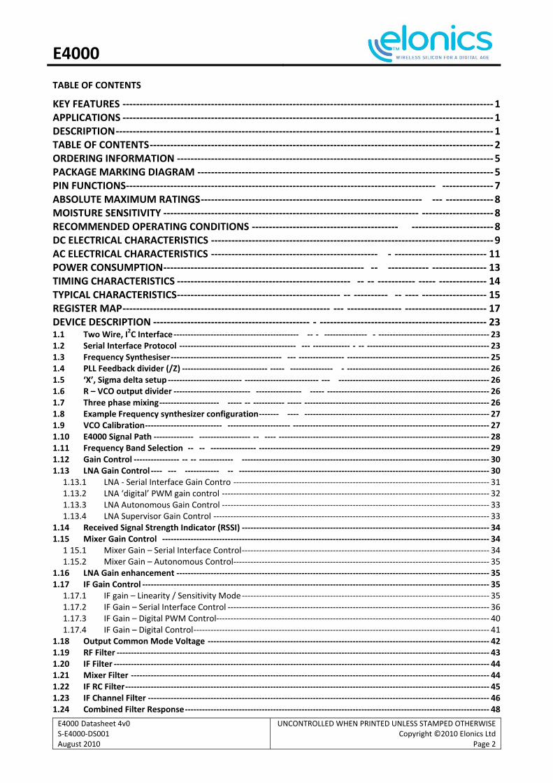
BLOCK DIAGRAM

E4000
E4000 Datasheet 4v0 S‐E4000‐DS001 August 2010
UNCONTROLLED WHEN PRINTED UNLESS STAMPED OTHERWISECopyright ©2010 Elonics Ltd
Page 5
ORDERING INFORMATION
Order Code Ambient Temperature Range
Package Moisture Sensitivity Level
Peak Soldering Temperature
E4000EQG ‐40 to +85 °C QFN‐32 5x5mm body (Pb‐free)
MSL1 260°C
E4000EQGD ‐40 to +85 °C QFN‐32 5x5mm body (Pb‐free , dry packed and vacuum sealed)
MSL1 260°C
E4000EQGR ‐40 to +85 °C QFN‐32 5x5mm body (Pb‐free, tape and reel)
MSL1 260°C
Notes
1) Tube quantity = 95
2) Reel quantity = 3500
PACKAGE MARKING DIAGRAM
Line 1 Elonics Logo – Fixed
Line 2 E4000 – Fixed (Device Name) EQG ‐ Fixed
Line 3 YYWW – Variable (Date Code) Z – Variable (Trace code e.g. A, B, C … X, Y, Z – lots molded in the same work week MMC –Variable (Manufacturing code)
E4000EQG YYWWZMMC

E4000
E4000 Datasheet 4v0 S‐E4000‐DS001 August 2010
UNCONTROLLED WHEN PRINTED UNLESS STAMPED OTHERWISECopyright ©2010 Elonics Ltd
Page 6
PIN INFORMATION
Top view
AGND
VBG
REXT
RFSHIELD
RFIN
LNAGND
LNAGND2
LNAVDD
QVOUTP
CKOUTN
GAIN0
ST
BY
B
IVOUTP
GAIN1
IVOUTN
CKOUTP
IFG
ND
A0
IFV
DD
QVOUTN
PL
L_V
DD
XT
AL
PL
L_G
ND
S
CL
K
SD
AT
PD
NB
A1
AV
DD
CL
OC
KIN
TU
N_
DG
ND
1
TU
N_
DG
ND
0
TU
N_
DV
DD
Elonics E4000
QFN32 5x5mm
1
E4000
E4000 Datasheet 4v0 S‐E4000‐DS001 August 2010
UNCONTROLLED WHEN PRINTED UNLESS STAMPED OTHERWISECopyright ©2010 Elonics Ltd
Page 7
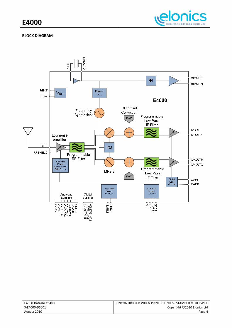
PIN FUNCTIONS
Pin Name Type Description
1 AGND Ground 0V. Connect to Tuner analogue ground
2 VBG Analogue Output Band gap voltage. A 10nF decoupling capacitor should be placed between this pin and 0V. The capacitor should be placed close to this pin.
3 REXT Analogue Output Reference current generation. A 10k, 1%, resistor should be placed between this pin and 0V.
4 RFSHIELD Ground RF Shield, connect to LNAGND
5 RFIN Analogue Input RF input. 50R impedance.
6 LNAGND Ground 0V
7 LNAGND2 Ground 0V, connect to LNAGND
8 LNAVDD Supply 1.5V
9 IFVDD Supply 1.5V
10 IFGND Ground 0V
11 A0 Digital Input Tuner I2C device address control (bit 0). (3 3V tolerant).
12 A1 Digital Input Tuner I2C device address control (bit 1). (3.3V tolerant).
13 STBYB Digital Input Normal operation = 1.5V (3.3V tolerant). Standby = 0V. If unused, connect AVDD
14 PDNB Digital Input Normal operation = 1.5V 3.3V tolerant). Power down = 0V. If unused, connect AVDD
15 SDAT Digital I / O I2C data. Pull up to 1 5V (3.3V tolerant). Pull up resistor > 4.5kΩ
16 SCLK Digital Input I2C clock input. (3V3 tolerant).
17 QVOUTN Analogue Output Q Channe Output ‐ve
18 QVOUTP Analogue Output Q Channe Output +ve
19 IVOUTN Analogue Output I Channel Output ‐ve
20 IVOUTP Analogue Output I Channel Output +ve
21 GAIN0 Digital/PWM Gain control input. Either digital IF or IF PWM input (3V3 tolerant).
22 GAIN1 Digital/PWM Gain control input. Either digital IF or RF PWM input (3V3 tolerant).
23 CKOUTN LVDS or CMOS output
Clock Output –ve. If unused, should be left as ‘no connect’.
24 CKOUTP LVDS or CMOS output
Clock Output +ve. If unused, should be left as ‘no connect’.
25 TUN_DVDD Supply 1.5V
26 TUN_DGND0 Ground 0V
27 TUN_DGND1 Ground 0V
28 CLOCKIN Oscillator Connect to crystal OR Clock input from external source (1.5V logic levels).
29 XTAL Oscillator Connect to crystal. If unused, should be left as ‘no connect’.
30 PLL_GND Ground 0V. Do not connect directly to LNAGND
31 PLL_VDD Supply 1.5V
32 AVDD Supply 1.5V

E4000
E4000 Datasheet 4v0 S‐E4000‐DS001 August 2010
UNCONTROLLED WHEN PRINTED UNLESS STAMPED OTHERWISECopyright ©2010 Elonics Ltd
Page 8
ABSOLUTE MAXIMUM RATINGS
Condition Min Max Units
Storage Temperature ‐65 +150 °C
Supply Voltage (LNAVDD, PLL_VDD, IFVDD, TUN_DVDD, AVDD)
GND ‐ 0.3 GND + 1.65 V
Analogue Inputs/Outputs GND ‐ 0.3 AVDD +0.3 V
Digital Inputs GND ‐ 0.3 +3.6 V
I2C Interface Inputs GND ‐ 0.3 +3.6 V
RF Input Power +10 dBm
Lead Temperature (10s soldering) +260 C
Stresses beyond those listed may cause permanent damage to the device or may impair device reliability. The device should be operated within ‘recommended operating conditions’.
This is an ESD Sensitive Device manufactured in a CMOS process. It is therefore susceptible to damage from excessive voltage such as is caused by static discharge. Proper ESD precautions must be taken during handling, storage and operation of this device MOISTURE SENSITIVITY
Devices are qualified to IPC/JEDEC J‐STD‐020B, determining moisture sensitivity and acceptable storage conditions. The rating of this product is as indicated within the Ordering Information section of this datasheet. RECOMMENDED OPERATING CONDITIONS
Condition Min Typ Max Units
Operating Temperature ‐40 +25 +85 °C
Supply Voltage (TUN_DVDD, LNAVDD, PLL_VDD, IFVDD, AVDD)
+1.4 +1.5 +1.6 V
Ground Voltage 0 V
Analogue Inputs 0 +1.6 V
Digital Inputs (Except CLOCKIN, pin 28) 0 +3.6 V
CLOCKIN 0.7 +1.6 V
Device Function and Electrical Characteristics can only be maintained if operating conditions are adhered to.
E4000
E4000 Datasheet 4v0 S‐E4000‐DS001 August 2010
UNCONTROLLED WHEN PRINTED UNLESS STAMPED OTHERWISECopyright ©2010 Elonics Ltd
Page 9
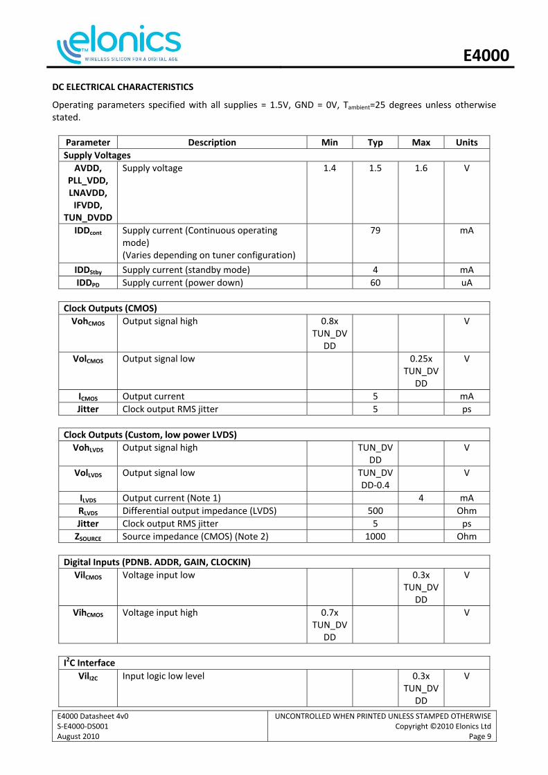
DC ELECTRICAL CHARACTERISTICS
Operating parameters specified with all supplies = 1.5V, GND = 0V, Tambient=25 degrees unless otherwise stated.
Parameter Description Min Typ Max Units
Supply Voltages
AVDD, PLL_VDD, LNAVDD, IFVDD,
TUN_DVDD
Supply voltage 1.4 1.5 1.6 V
IDDcont Supply current (Continuous operating mode) (Varies depending on tuner configuration)
79 mA
IDDStby Supply current (standby mode) 4 mA
IDDPD Supply current (power down) 60 uA
Clock Outputs (CMOS)
VohCMOS Output signal high 0.8x TUN_DV
DD
V
VolCMOS Output signal low 0.25x TUN_DV
DD
V
ICMOS Output current 5 mA
Jitter Clock output RMS jitter 5 ps
Clock Outputs (Custom, low power LVDS)
VohLVDS Output signal high TUN_DVDD
V
VolLVDS Output signal low TUN_DVDD‐0.4
V
ILVDS Output current (Note 1) 4 mA
RLVDS Differential output impedance (LVDS) 500 Ohm
Jitter Clock output RMS jitter 5 ps
ZSOURCE Source impedance (CMOS) (Note 2) 1000 Ohm
Digital Inputs (PDNB. ADDR, GAIN, CLOCKIN)
VilCMOS Voltage input low 0.3x TUN_DV
DD
V
VihCMOS Voltage input high 0.7x TUN_DV
DD
V
I2C Interface
VilI2C Input logic low level 0.3x TUN_DV
DD
V

E4000
E4000 Datasheet 4v0 S‐E4000‐DS001 August 2010
UNCONTROLLED WHEN PRINTED UNLESS STAMPED OTHERWISECopyright ©2010 Elonics Ltd
Page 10
VihI2C Input logic high level 0.7x TUN_DV
DD
V
VolI2C Output logic level low (Note 3) 0.4 V
NOTES 1. LVDS output current is programmable. 2. If load impedance is different may require a termination resistor. 3. Pull up resistor on I2C data line should be >4k7 Ohms.

E4000
E4000 Datasheet 4v0 S‐E4000‐DS001 August 2010
UNCONTROLLED WHEN PRINTED UNLESS STAMPED OTHERWISECopyright ©2010 Elonics Ltd
Page 11
AC ELECTRICAL CHARACTERISTICS
RF
FIN Input Frequency Range 64 1700 MHz
NFFM Noise figure (FM) 4.5 dB
NFVHF Noise figure (VHF) 4.5 dB
NFUHF Noise Figure (UHF) 3.8 dB
NFL‐BAND Noise figure (L‐Band) 4.3 dB
IIP3 Input referred IP3 point (minimum gain) 5 dBm
S1150R Input Return loss (50R system) ‐15 dB
S1175R Input return loss (75R system) ‐20 dB
Programmable RF tracking Filter (Note 4)
FC RF Filter Centre Frequency (programmable between)
350 1700 MHz
F3BW RF Filter 3dB Bandwidth 200 MHz
FREJ RF out of band rejection (>150% FC) 10 dB
Typical Gain (Note 5)
Gt Total Gain range 2 99 dB
G1 LNA Gain Range ‐5 30 dB
G2 Mixer Gain Range 4 12 dB
G3 IF Gain Range 4 57 dB
ΔG3 Step Size 1 dB
Gf Gain flatness (IF frequency band) (Note 6) ±1dB dB
Reference oscillator
Fosc Frequency 16 26 32 MHz
Cosc Load (presented by E4000) 10 pF
Posc Crystal power capability 100 µW
NOTES 4. RF filters track with LNA onfiguration. When operating at f< 240MHz filter is low pass type. For f>350MHz filter is band pass type 5. Gain is programmab e. Values quoted detail the typical range to which gains can be set. 6. Filters minimised. DC – 4MHz
Frequency Synthesiser (Note 7)
FVCO VCO frequency range 2600 3900 MHz
/R R (VCO output) divider ratio 2 48
FLO Local Oscillator Frequency Range 64 1700 MHz
FΔLO Local Oscillator Frequency Step Size(Note8) 10 20000 Hz
Integrated phase noise (1kHz – 8MHz) -29 dBc
Phase Noise @ 10kHz -80 dBc /Hz
Phase Noise @ 2MHz -125 dBc /Hz
/Z Z (phase detector) divide ratio 64 255

E4000
E4000 Datasheet 4v0 S‐E4000‐DS001 August 2010
UNCONTROLLED WHEN PRINTED UNLESS STAMPED OTHERWISECopyright ©2010 Elonics Ltd
Page 12
IF Channel Filtering
Fc Channel Filter corner frequency (Note 9) 2.15 5.50 MHz
A20M Attenuation at 10MHz (fc=4MHz,) 70 dB
IQ Baseband Outputs
Vpp Differential Peak to Peak Output Voltage 1000 mV
Vcm Common Mode Voltage (Note 10) 0.58 V
Rout Single Ended Output Impedance 250 Ohm
Load Output load 15k Ohm
Output load capacitance 10 pF
AIMB Differential I to Q Amplitude Imbalance 0.2 dB
PIMB Differential I to Q Phase Imbalance 5 degree
NOTES 7. Section 1.3 documents Frequency Synthesizer configuration for various states. 8. LO frequency step size varies depending on /R ratio set. 9. Programmable with 0.2MHz step size. 10. Common mode output voltage is programmable
E4000
E4000 Datasheet 4v0 S‐E4000‐DS001 August 2010
UNCONTROLLED WHEN PRINTED UNLESS STAMPED OTHERWISECopyright ©2010 Elonics Ltd
Page 13
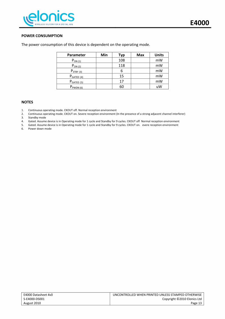
POWER CONSUMPTION
The power consumption of this device is dependent on the operating mode.
Parameter Min Typ Max Units
PON (1) 108 mW
PON (2) 118 mW
PSTBY (3) 6 mW
PGATED (4) 15 mW
PGATED (5) 17 mW
PPWDN (6) 60 uW
NOTES
1. Continuous operating mode. CKOUT off. Normal reception environment 2. Continuous operating mode. CKOUT on. Severe reception environment (In the presence of a strong adjacent channel interferer) 3. Standby mode 4. Gated. Assume device is in Operating mode for 1 cycle and Standby for 9 cycles. CKOUT off Normal reception environment 5. Gated. Assume device is in Operating mode for 1 cycle and Standby for 9 cycles. CKOUT on. evere reception environment 6. Power down mode
E4000
E4000 Datasheet 4v0 S‐E4000‐DS001 August 2010
UNCONTROLLED WHEN PRINTED UNLESS STAMPED OTHERWISECopyright ©2010 Elonics Ltd
Page 14
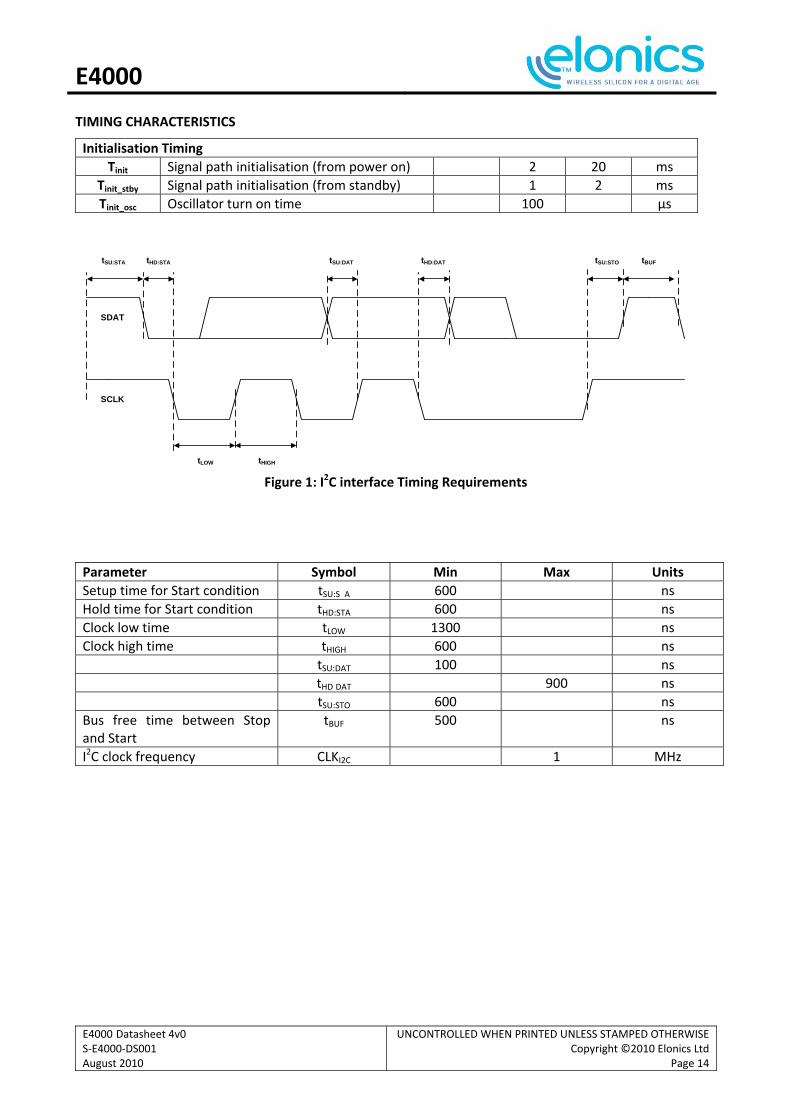
TIMING CHARACTERISTICS
Initialisation Timing
Tinit Signal path initialisation (from power on) 2 20 ms
Tinit_stby Signal path initialisation (from standby) 1 2 ms
Tinit_osc Oscillator turn on time 100 μs
tSU:STA tHD:STA
tHIGHtLOW
tSU:DAT tHD:DAT tBUFtSU:STO
SDAT
SCLK
Figure 1: I2C interface Timing Requirements
Parameter Symbol Min Max Units
Setup time for Start condition tSU:S A 600 ns
Hold time for Start condition tHD:STA 600 ns
Clock low time tLOW 1300 ns
Clock high time tHIGH 600 ns
tSU:DAT 100 ns
tHD DAT 900 ns
tSU:STO 600 ns
Bus free time between Stop and Start
tBUF 500 ns
I2C clock frequency CLKI2C 1 MHz

E4000
E4000 Datasheet 4v0 S‐E4000‐DS001 August 2010
UNCONTROLLED WHEN PRINTED UNLESS STAMPED OTHERWISECopyright ©2010 Elonics Ltd
Page 15
TYPICAL CHARACTERISTICS
Operating parameters are specified for all supplies = 1.5V, GND = 0V, Tambient=25 degrees unless otherwise stated.
Supply current vs. RF input power to tuner (maintaining 1Vp‐p differential output amplitude)
Supply curren vs. ope ating frequency
Supply current vs. operating voltage
E4000 gain vs. frequency (normalised)
IIP3 vs. RF input power (E4000 gains set to maintain 1Vp‐p diff output swing)
7072
74767880
8284
-100 -80 -60 -40 -20 0
RF input power (dBm)
Su
pp
ly c
urr
ent
(mA
)
71
7273
7475
7677
7879
80
0 500 1000 1500 2000
Frequency (MHz)
Supply
curr
ent (m
A)
72
7374
7576
77
1.4 1.45 1.5 1.55 1.6
Supply voltage (V)
Su
pp
ly c
urr
ent
(mA
)
-10
-5
0
5
10
0 400 800 1200 1600
Frequency (MHz)
Gai
n (
dB
)
-80
60
40
20
0
20
-100 -80 -60 -20 0
RF input power (dBm)
IIP3
(dB
m)
Baseband channel filter can be disabled at low input power, reducing supply current

E4000
E4000 Datasheet 4v0 S‐E4000‐DS001 August 2010
UNCONTROLLED WHEN PRINTED UNLESS STAMPED OTHERWISECopyright ©2010 Elonics Ltd
Page 16
Return loss vs. frequency vs. LNA gain setting (75R environment).
Return loss vs. frequency vs. LNA gain setting (50R environment)
Programmable, baseband channel filter frequency response, (4.1MHz filter corner frequency setting is shown)
Programmable, RF filter frequency response, (666MHz setting is shown).
Local oscillator phase noise vs. frequency offset from carrier
-60
-50
-40
-30
-20
-10
0
0 500 1000 1500 2000
Frequency (MHz)
S11
(dB
)
-30
-25
-20
-15
-10
-5
0
0 500 1000 1500 2000
Frequency (MHz)
S11
(d
B)
-80.00
-60.00
-40.00
-20.00
0.00
0 5 10 15 20
Frequency (MHz)
Att
enu
atio
n (
dB
)
-10
-9
-8
-7
-6
-5-4
-3
-2
-1
0
400 500 600 700 800 900
Frequency (MHz)
Att
enu
atio
n (
dB
)
-130
-120
-110
-100
-90
-80
-70
-60
1000 10000 100000 1000000
Frequency offset from carrier (Hz)
Ph
ase
no
ise
(dB
c/H
z)
LNA gain = 25dB
LNA gain = 0dB

E4000
E4000 Datasheet 4v0 S‐E4000‐DS001 August 2010
UNCONTROLLED WHEN PRINTED UNLESS STAMPED OTHERWISECopyright ©2010 Elonics Ltd
Page 17
REGISTER MAP
Colour Explanation Green Reserved register Yellow User control register R/W Purple User control register R Blue User should not over-write default values
Bit number
Address 7 (MSB)
6 5 4 3 2 1 0 (LSB)
0x00h ‘Master 2’
Reserved Default = 00000
POR detect = 1 after a reset.
Write 1 to clear
register
Standb 1=normal operation 0 = standby
mode
RESET 1=reset 0=normal operation
0x01h ‘Master2’
Reserved Default = 00000000
0x02h ‘Master3’
Elonics identifier Default = 01000000
0x03h ‘Master4’
Elonics identifier Default = 00000000
0x04h ‘Master5’
Elonics identifier Default = 00000011
0x05h ‘Input clock’
Reserved Default=0000000
E4000 Clock select 00 = Crystal clock source
(default) 01= Divided PLL
Do not write to this register
0x06h ‘Reference
clock’
Reserved Default=000
Output clock frequency 00 = Cry tal freq ÷ 1
(default) 01= Crystal freq ÷ 2 10 = Crystal freq ÷ 4
Clock output logic
0=LVDS 1=CMOS (default)
CMOS configuration Or
LVDS drive strength
See 1.28
0x07h ‘Synth1’
Reserved Default = 000
Input clock freq range 00=16‐32MHz (default)
Always write 00
Frequency band 00=VHF II 01=VHF III
10=UHF(default) 11=L band
PLL locked 1=locked
0x08h ‘Synth2’
Reserved Default=00000000
0x09h ‘Synth3’
Feedback divider ‘/Z’ See section 1.4
0x0ah ‘Synth ’
Sigma delta ‘X’ (LSB) See section 1.5
0x0bh ‘Synth5’
Sigma delta ‘X’ (MSB) See section 1.5
0x0dh ‘Synth7’
Reserved Default=00000
Enable 3 phase mixing
0=disable (default) See 1.7
VCO output divider ‘/R’ Default =001 See section 1.6

E4000
E4000 Datasheet 4v0 S‐E4000‐DS001 August 2010
UNCONTROLLED WHEN PRINTED UNLESS STAMPED OTHERWISECopyright ©2010 Elonics Ltd
Page 18
Bit number
Address 7
6 5 4 3 2 1 0
0x0eh ‘Synth8’
Reserved Default =00
VCO cal warning flag
VCO range low flag.
User should update loop when a value 1 is read (bit 2)
VCO range high flag
User should update loop when a value 1 is read (bit 2)
VCO cal update
Write 1 to update when in supervisor mode
VCO cal mode 00= auto cal off
01=auto cal on (default) 10=supervisor mode
11=auto cal off
0x0fh ‘Synth9’
Reserved Default=0000
VCO range Default = 1000
0x10h ‘filt1’
Reserved Default=0000
RF filter Default = 0000 See section 1 19
0x11h ‘filt2’
Mixer filter Default=0000
See section 1.21
IF C filt r Defaul =0000
See section 1.22
0x12h ‘filt3’
Reserved Default=00
Filter disable 1=disable 0=enable (default) See 0
IF channel filter Default = 00000 See section 0
0x14h ‘Gain1’
Reserved Default=0000
LNA gain 00X0=‐5dB (default)
00X1=‐2.5dB 0100=0dB 0101=2.5dB 0110=5dB 0111=7.5dB 1000=10dB 1001=12.5dB 1010=15dB 1011=17.5dB 1100=20dB 1101=25dB 111X=30dB
See section1.13.1
0x15h ‘Gain2’
Reserved Default=0000000
Mixer gain 0=4dB (default)
1=12dB See 1.15
0x16h ‘Gain3’
Reserved Default=0
IF stage 4 gain 00=0dB 01=1dB 10=2dB(default)
11=3dB See section 0
IF stage 3 gain 00=0dB 01=3dB(default)
10=6dB 11=9dB
See section 0
IF stage 2 gain 00=0dB 01=3dB
10=6dB 11=9dB(default) See section 0
IF stage 1 gain
0=‐3dB 1=6dB(defa
ult) See 0
0x17h ‘Gain4’
Reserved Default=00
IF stage 6 gain 000=3dB(default)
001=6dB 010=9dB 011=12dB 100=15dB
See section 0
IF stage 5 gain 000=3dB(default)
001=6dB 010=9dB 011=12dB 100=15dB
See section 0

E4000
E4000 Datasheet 4v0 S‐E4000‐DS001 August 2010
UNCONTROLLED WHEN PRINTED UNLESS STAMPED OTHERWISECopyright ©2010 Elonics Ltd
Page 19
Bit number
Address 7
6 5 4 3 2 1 0
0x1Ah ‘AGC1’
LNA gain high flag
User should update loop when a value 1 is read (bit 5)
LNA gain low flag
User should update loop when a value 1 is read (bit 5)
LNA update Write 1 to update in supervise mode
Linearity mode
See section 1.17.1
Default = 1
Gain control mode See section 1.12 Default = 0000
0x1Bh ‘AGC2’
LNA autonomous control – calibration value
0x1Ch ‘AGC3’
Received signal strength indicator See section 0
0x1Dh ‘AGC4’
LNA – autonomous control – High threshold Write threshold value when E4000 is initialised
0x1Eh ‘AGC5’
LNA – autonomous control – Low threshold Write threshold value when E4000 is initialised
0x1Fh ‘AGC6’
Reserved Default = 0
Reserved Always write = 00
LNA calibration request
LNA – autonomous control – Averaging time Default=0000 See 1.13.3
0x20h ‘AGC7’
Reserved Default = 00
RF gain control – gain step size 0 = 2.5dB
(default) 1 = 5dB
Mixer threshold See 1.15.2
Mixer gain control mode 1 = auto
0x21h ‘AGC8’
Sensitivity / Linearity mode switch point Default = 0101101 (45dB)
See section 1.17 1
Sensitivity / linearity mode – control 1 = auto control 0 = user control (default)
0x24h ‘AGC11’
Reserved Default = 00000
LNA gain enhancement level Default = 00
LNA gain enhance enable
0x25h ‘AGC11’
Reserved Default = 000000
Linearity monitor reset flag
Do not write to this register
Linearity monitor flag Do not write
to this register
0x29h ‘DC1’
Reserved Default = 0000000
DC offset cal request
Write 1 See section 0
0x2Ah ‘DC2’
Reserved Default = 00
I channel DC offset See section 0
0x2Bh ‘DC3’
Reserved Default = 00
Q channel DC offset See section 0
0x2Ch ‘DC4’
Reserved Default = 00
Q channel offset range See section 0
Reserved Default = 00
I channel offset range See section 0
E4000
E4000 Datasheet 4v0 S‐E4000‐DS001 August 2010
UNCONTROLLED WHEN PRINTED UNLESS STAMPED OTHERWISECopyright ©2010 Elonics Ltd
Page 20
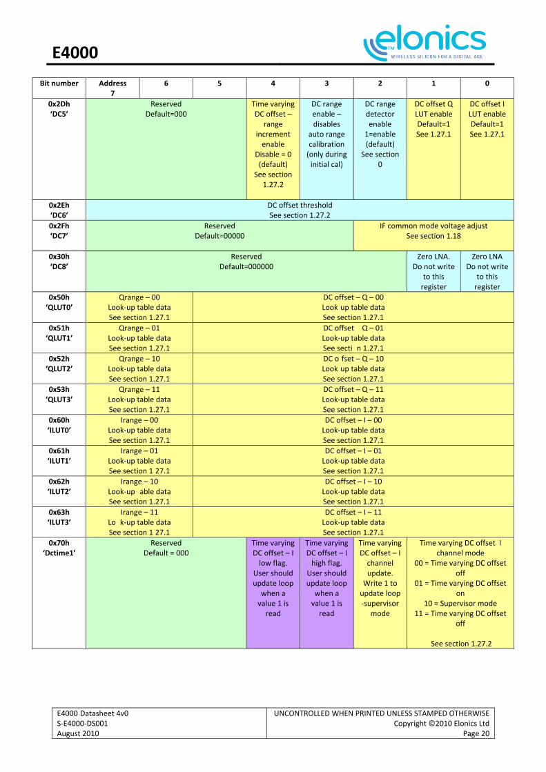
Bit number
Address 7
6 5 4 3 2 1 0
0x2Dh ‘DC5’
Reserved Default=000
Time varying DC offset –
range increment enable
Disable = 0 (default)
See section 1.27.2
DC range enable – disables
auto range calibration (only during initial cal)
DC range detector enable 1=enable (default)
See section 0
DC offset Q LUT enable Default=1 See 1.27.1
DC offset I LUT enable Default=1 See 1.27.1
0x2Eh ‘DC6’
DC offset threshold See section 1.27.2
0x2Fh ‘DC7’
Reserved Default=00000
IF common mode voltage adjust See section 1.18
0x30h ‘DC8’
Reserved Default=000000
Zero LNA. Do not write
to this register
Zero LNA Do not write
to this register
0x50h ‘QLUT0’
Qrange – 00 Look‐up table data See section 1.27.1
DC offset – Q – 00 Look up table data See section 1.27.1
0x51h ‘QLUT1’
Qrange – 01 Look‐up table data See section 1.27.1
DC offset Q – 01 Look‐up table data See secti n 1.27.1
0x52h ‘QLUT2’
Qrange – 10 Look‐up table data See section 1.27.1
DC o fset – Q – 10 Look up table data See section 1.27.1
0x53h ‘QLUT3’
Qrange – 11 Look‐up table data See section 1.27.1
DC offset – Q – 11 Look‐up table data See section 1.27.1
0x60h ‘ILUT0’
Irange – 00 Look‐up table data See section 1.27.1
DC offset – I – 00 Look‐up table data See section 1.27.1
0x61h ‘ILUT1’
Irange – 01 Look‐up table data See section 1 27.1
DC offset – I – 01 Look‐up table data See section 1.27.1
0x62h ‘ILUT2’
Irange – 10 Look‐up able data See section 1.27.1
DC offset – I – 10 Look‐up table data See section 1.27.1
0x63h ‘ILUT3’
Irange – 11 Lo k‐up table data See section 1 27.1
DC offset – I – 11 Look‐up table data See section 1.27.1
0x70h ‘Dctime1’
Reserved Default = 000
Time varying DC offset – I low flag.
User should update loop when a value 1 is read
Time varying DC offset – I high flag.
User should update loop when a value 1 is read
Time varying DC offset – I channel update. Write 1 to update loop ‐supervisor
mode
Time varying DC offset I channel mode
00 = Time varying DC offset off
01 = Time varying DC offset on
10 = Supervisor mode 11 = Time varying DC offset
off
See section 1.27.2

E4000
E4000 Datasheet 4v0 S‐E4000‐DS001 August 2010
UNCONTROLLED WHEN PRINTED UNLESS STAMPED OTHERWISECopyright ©2010 Elonics Ltd
Page 21
Bit number
Address 7
6 5 4 3 2 1 0
0x71h ‘Dctime2’
Reserved Default = 000
Time varying DC offset – Q low flag. User should update loop when a value 1 is read
Time varying DC offset – Q high flag. User should update loop when a value 1 is read
Time varying DC offset – Q channel update. Write 1 to update loop ‐ supervisor
mode
Time varying DC offset Q channel mode
00 = Time varying DC offset off
01 = Time varying DC offset on
10 = Supervisor mode 11 = Time varying DC offset
off See section 1.27.2
0x72h ‘Dctime3’
Time varying DC offset threshold See section 1.27.2
Do not write to this register
0x73h ‘Dctime4’
Reserved Default = 00000
Time varying DC offset – timer control See section 1.27.2
Do not write to this register
0x74h ‘PWM1’
PWM upper threshold – Gain0 Default = 00000011 See section 1.17.3
0x75h ‘PWM2’
PWM lower threshold – Ga n0 Default = 11111100 See section 1.17.3
0x76h ‘PWM3’
PWM upper threshold – Gain1 Default = 00000011 Se section 1.13.2
0x77h ‘PWM4’
PWM lower threshold – Gain1 Default = 11111100 See section 1 13.2
0x78h ‘Bias’
Reserved Default = 000000
Quadgen driver bias Default =11
Reference current control See section 1.11
0x79h Rese ved Default = 0000
Quadgen bias Default = 00
Reference current control Do not write to this register
Divider bias Default = 00
Reference current control Do not write to this register
0x7ah Clock output power down key Writing 10010110 will power down E4000 clock output
See section 0
0x7bh Cont ol bit Always write
0
Channel filter calibration value See section 0
Channel filter cal. Write 1 to instruct a calibration
0x7dh Reserved Default = 0000000
I2C register address – address increment See 1.3
E4000
E4000 Datasheet 4v0 S‐E4000‐DS001 August 2010
UNCONTROLLED WHEN PRINTED UNLESS STAMPED OTHERWISECopyright ©2010 Elonics Ltd
Page 22
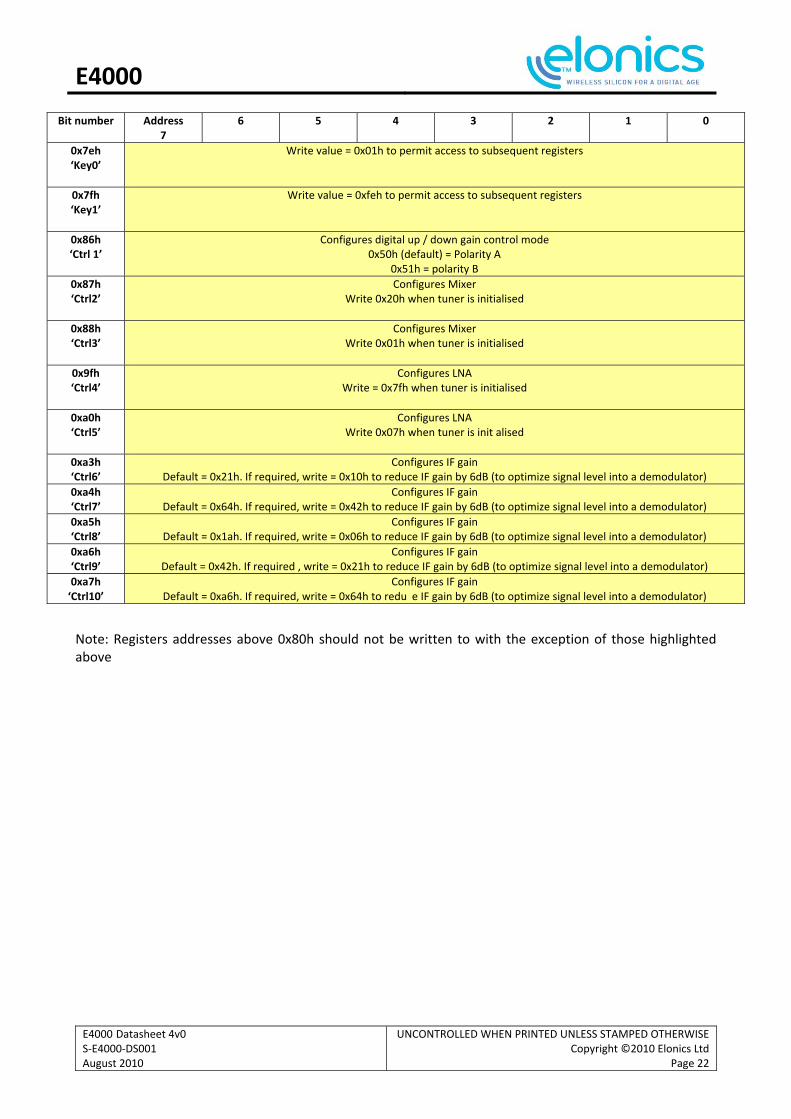
Bit number
Address 7
6 5 4 3 2 1 0
0x7eh ‘Key0’
Write value = 0x01h to permit access to subsequent registers
0x7fh ‘Key1’
Write value = 0xfeh to permit access to subsequent registers
0x86h ‘Ctrl 1’
Configures digital up / down gain control mode 0x50h (default) = Polarity A
0x51h = polarity B
0x87h ‘Ctrl2’
Configures Mixer Write 0x20h when tuner is initialised
0x88h ‘Ctrl3’
Configures Mixer Write 0x01h when tuner is initialised
0x9fh ‘Ctrl4’
Configures LNA Write = 0x7fh when tuner is initialised
0xa0h ‘Ctrl5’
Configures LNA Write 0x07h when tuner is init alised
0xa3h ‘Ctrl6’
Configures IF gain Default = 0x21h. If required, write = 0x10h to reduce IF gain by 6dB (to optimize signal level into a demodulator)
0xa4h ‘Ctrl7’
Configures IF gain Default = 0x64h. If required, write = 0x42h to reduce IF gain by 6dB (to optimize signal level into a demodulator)
0xa5h ‘Ctrl8’
Configures IF gain Default = 0x1ah. If required, write = 0x06h to reduce IF gain by 6dB (to optimize signal level into a demodulator)
0xa6h ‘Ctrl9’
Configures IF gain Default = 0x42h. If required , write = 0x21h to reduce IF gain by 6dB (to optimize signal level into a demodulator)
0xa7h ‘Ctrl10’
Configures IF gain Default = 0xa6h. If required, write = 0x64h to redu e IF gain by 6dB (to optimize signal level into a demodulator)
Note: Registers addresses above 0x80h should not be written to with the exception of those highlighted above
E4000
E4000 Datasheet 4v0 S‐E4000‐DS001 August 2010
UNCONTROLLED WHEN PRINTED UNLESS STAMPED OTHERWISECopyright ©2010 Elonics Ltd
Page 23
DEVICE DESCRIPTION
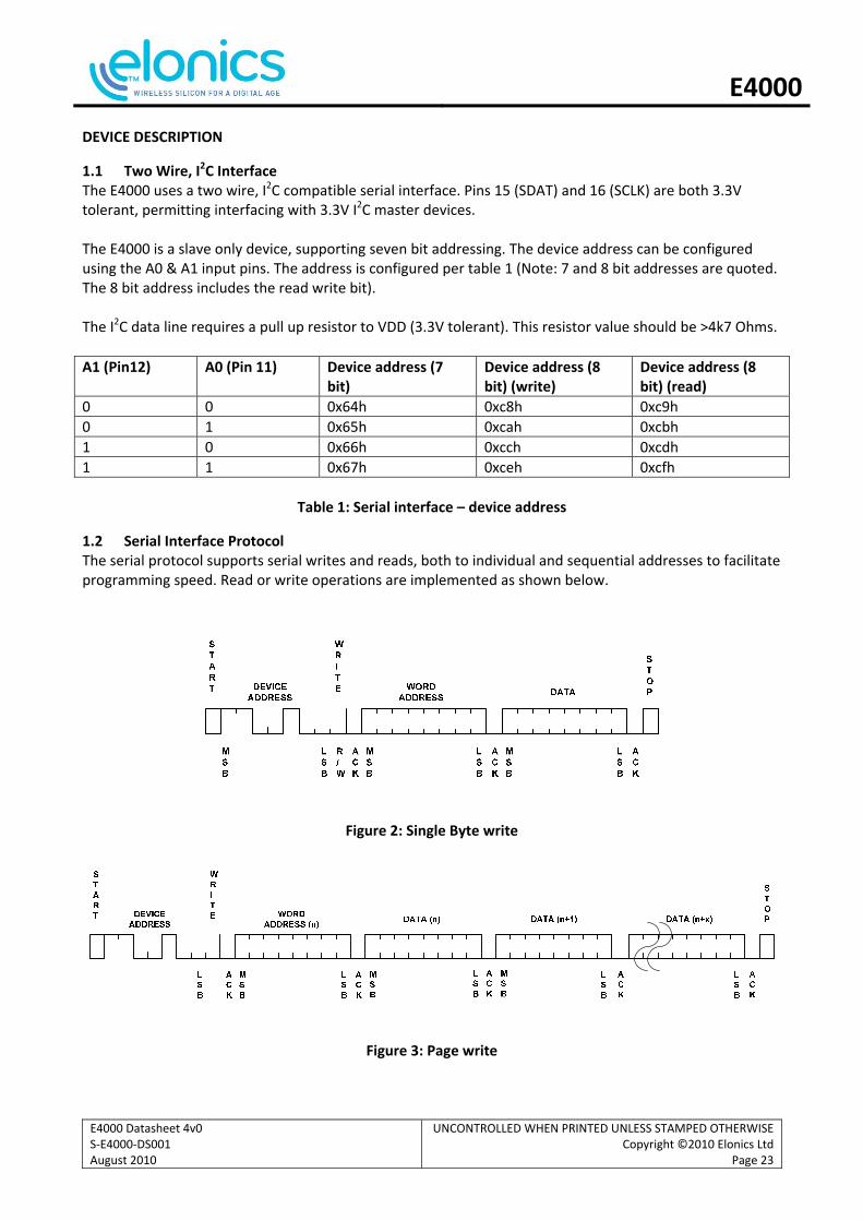
1.1 Two Wire, I2C Interface The E4000 uses a two wire, I2C compatible serial interface. Pins 15 (SDAT) and 16 (SCLK) are both 3.3V tolerant, permitting interfacing with 3.3V I2C master devices. The E4000 is a slave only device, supporting seven bit addressing. The device address can be configured using the A0 & A1 input pins. The address is configured per table 1 (Note: 7 and 8 bit addresses are quoted. The 8 bit address includes the read write bit). The I2C data line requires a pull up resistor to VDD (3.3V tolerant). This resistor value should be >4k7 Ohms.
Table 1: Serial interface – device address
1.2 Serial Interface Protocol The serial protocol supports serial writes and reads, both to individual and sequential addresses to facilitate programming speed. Read or write operations are implemented as shown below.
Figure 2: Single Byte write
Figure 3: Page write
A1 (Pin12) A0 (Pin 11) Device address (7 bit)
Device address (8 bit) (write)
Device address (8 bit) (read)
0 0 0x64h 0xc8h 0xc9h
0 1 0x65h 0xcah 0xcbh
1 0 0x66h 0xcch 0xcdh
1 1 0x67h 0xceh 0xcfh

E4000
E4000 Datasheet 4v0 S‐E4000‐DS001 August 2010
UNCONTROLLED WHEN PRINTED UNLESS STAMPED OTHERWISECopyright ©2010 Elonics Ltd
Page 24
Figure 4: Single byte read
Figure 5: Sequen ial read
A dummy read or write command should be sent to the E4000 after the tuner is first powered on or is reset. This will not be ‘acknowledged’ but will configure the E4000 I2C interface. After this point I2C read and write commands behave normally. Register 0x7Dh [0] may be used to control whether a sequential read or write increments register address between each read. To configure to continuous read from the same register set this bit = 0. This feature may be useful to a user who wishes to continuously read the same register during operation of the tuner.

E4000
E4000 Datasheet 4v0 S‐E4000‐DS001 August 2010
UNCONTROLLED WHEN PRINTED UNLESS STAMPED OTHERWISECopyright ©2010 Elonics Ltd
Page 25
1.3 Frequency Synthesiser
Figure 6: Frequency Synthesizer architecture
The architecture of the E4000 Frequency synthesizer is shown in figure 6. This generates the local oscillator which is used in the mixer to down‐convert RF to baseband. The VCO output is divided by ‘R’ to generate the local oscillator for the down conversion mixer. The VCO output is also passed to the feedback divider, where its frequency is divided before being sent to the phase / frequency detector. The sigma delta dynamically dithers the division between ‘Z’ and alternative divider settings. This permits set ing of a non integer divider value giving high accuracy in the frequencies to which the local oscillator can be locked. The architecture of this divider ensures that the local oscillator maintains low phase noise across the range of settings. The phase detector compares the divided VCO frequency with the reference oscillator frequency and generates a tuning voltage to pull the VCO to the correct frequency. The divider and sigma delta values need to be set as per the formulae
fVCO = fOscillator * (Z + X/Y) (equation 1)
And
fLO = fVCO /R (equation 2) Where Y = 65536 and fOscillator is the crystal frequency (e.g. 26MHz). Values R, X, Y and Z are configurable using the tuner serial interface. To generate a 0Hz IF frequency, the local oscillator frequency should be set so that it is the same as the RF frequency. The VCO should be operated within the range of 2600 to 3900MHz.

E4000
E4000 Datasheet 4v0 S‐E4000‐DS001 August 2010
UNCONTROLLED WHEN PRINTED UNLESS STAMPED OTHERWISECopyright ©2010 Elonics Ltd
Page 26
1.4 PLL Feedback divider (/Z) The /N divider is controlled by register 0x09h. For example – to set N=99 Set 0x09h = 99(decimal)
1.5 ‘X’, Sigma delta setup The value of X is defined by registers 0x0Ah [7:0] (LSB) & 0x0Bh [7:0] (MSB). This can be set between 0 and 65535. For example, to set X = 5041 (5041 decimal = 13b1 hex) Register 0x0ah = b1h = 177 (decimal) Register 0x0bh = 13h = 19 (decimal)
1.6 /R – VCO output divider
The output divider, R, is set as per table 2. Note the difference in settings when using three phase mixing (described in section 1.7).
Output divider ‘/R’ [2:0] 0x0dh [2:0]
Division (3 phase mixing disabled)
Division (3 phase mixing enabled)
000 2 4
001 4 8
010 6 12
011 8 16
100 12 24
101 16 32
110 20 40
111 24 48
Table 2: Output divider
1.7 Three phase mixing Three phase mixing combines high speed clocks to create a local oscillator clock with slower edge speeds. This is used to reduce the high frequency harmonics, which when operating at low frequencies would be within the tuner bandwidth. This feature prevents interferer signals mixing with harmonics of the local oscillator frequency, increasing the dynamic range of the tuner.. It is recommended that three phase mixing should be used for VHF operation and not for UHF or L band operation. This is enabled or disabled using register 0x0Dh [3]. Note the effect enabling this feature has on the /R division as shown in table 2.
E4000
E4000 Datasheet 4v0 S‐E4000‐DS001 August 2010
UNCONTROLLED WHEN PRINTED UNLESS STAMPED OTHERWISECopyright ©2010 Elonics Ltd
Page 27
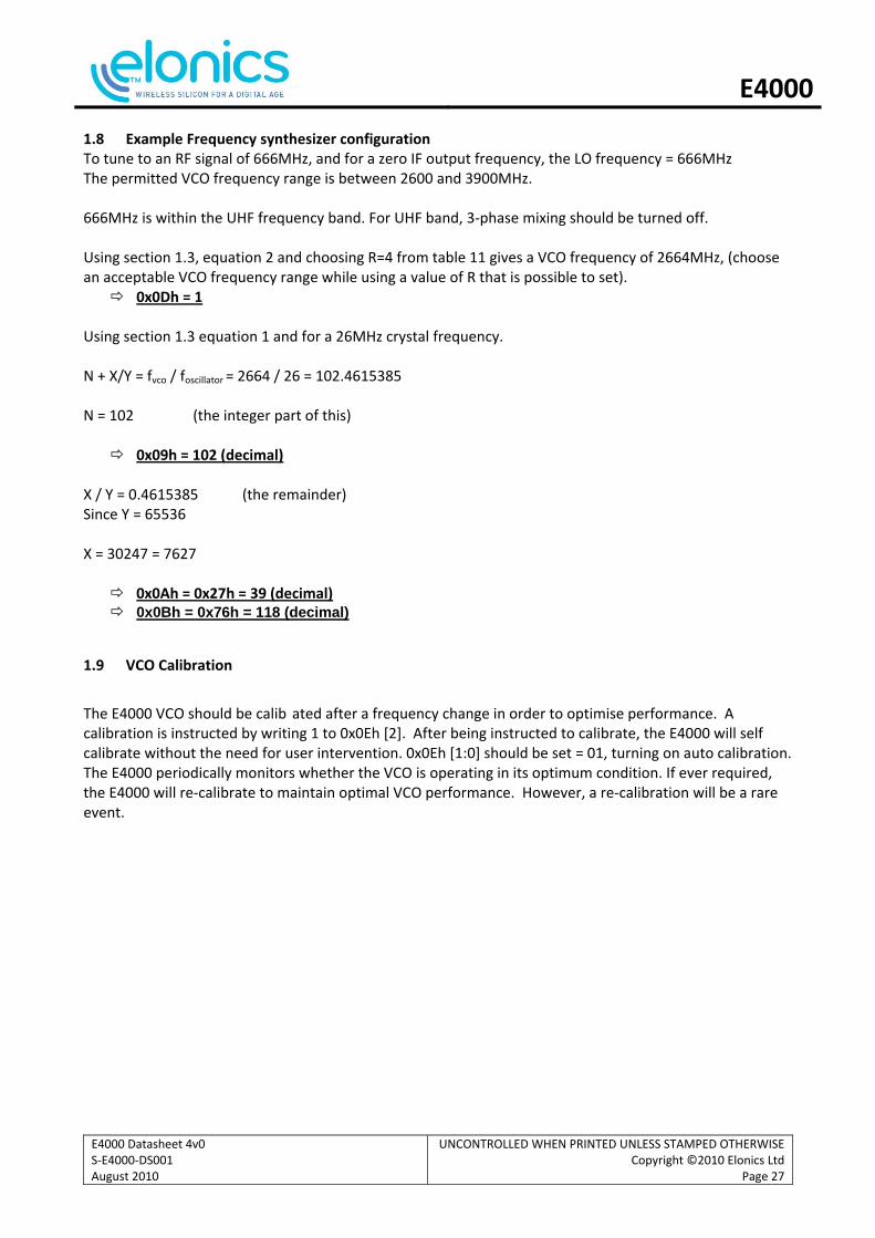
1.8 Example Frequency synthesizer configuration To tune to an RF signal of 666MHz, and for a zero IF output frequency, the LO frequency = 666MHz The permitted VCO frequency range is between 2600 and 3900MHz. 666MHz is within the UHF frequency band. For UHF band, 3‐phase mixing should be turned off. Using section 1.3, equation 2 and choosing R=4 from table 11 gives a VCO frequency of 2664MHz, (choose an acceptable VCO frequency range while using a value of R that is possible to set). 0x0Dh = 1
Using section 1.3 equation 1 and for a 26MHz crystal frequency. N + X/Y = fvco / foscillator = 2664 / 26 = 102.4615385 N = 102 (the integer part of this) 0x09h = 102 (decimal)
X / Y = 0.4615385 (the remainder) Since Y = 65536 X = 30247 = 7627 0x0Ah = 0x27h = 39 (decimal) 0x0Bh = 0x76h = 118 (decimal)
1.9 VCO Calibration
The E4000 VCO should be calib ated after a frequency change in order to optimise performance. A calibration is instructed by writing 1 to 0x0Eh [2]. After being instructed to calibrate, the E4000 will self calibrate without the need for user intervention. 0x0Eh [1:0] should be set = 01, turning on auto calibration. The E4000 periodically monitors whether the VCO is operating in its optimum condition. If ever required, the E4000 will re‐calibrate to maintain optimal VCO performance. However, a re‐calibration will be a rare event.

E4000
E4000 Datasheet 4v0 S‐E4000‐DS001 August 2010
UNCONTROLLED WHEN PRINTED UNLESS STAMPED OTHERWISECopyright ©2010 Elonics Ltd
Page 28
1.10 E4000 Signal Path
Figure 7: Block diagram of the E4000 signal path The E4000 signal path contains a wideband LNA (64MHz to 1 7GHz). The RF signal is filtered, reducing the effect of far out blocking signals. The signal is then down‐converted to baseband by the mixer, with I and Q phase channels generated. The IF signal is filtered to attenuate adjacent channel interferers. Signals are then amplified such that levels are optimal for sampling by the baseband’s ADCs. Tuner gain can be varied from 2 to 99dB providing a large dynamic range of signal reception. The LNA frequency response is optimised for different frequency bands as described in section 1.11. Gains can be controlled by various methods, as described in section 1.12. These include on chip autonomous control or baseband control using a PWM interface, digital up / down interface or using register writes via the 2C serial interface. Filters can be configured as described in section 1.19 to 0. Unwanted DC offsets in the IF gain path are eliminated as described in section 1.25.

E4000
E4000 Datasheet 4v0 S‐E4000‐DS001 August 2010
UNCONTROLLED WHEN PRINTED UNLESS STAMPED OTHERWISECopyright ©2010 Elonics Ltd
Page 29
1.11 Frequency Band Selection
The frequency band should be initialised as per table 3. This register configures the LNA to have optimum gain at the frequency of operation.
Band Register 0x07h [2:1]
VHF II (64 – 108MHz) 00
VHF III (170 – 240MHz) 01
UHF (default) (470 – 858MHz) 10
L (1452 – 1680MHz) 11
Table 3: Frequency band selection
When selecting frequency bands the user should also configure register 0x78h [1:0]. This sets bias currents used as references, such that the tuner is optimized for operation in the different frequency bands.
Band Register 0x78h [1:0]
VHF II (64 – 108M) 11
VHF III (170 – 240M) 11
UHF (default) (470 – 858MHz) 11
L (1452 – 1680MHz) 00
Table 4: Frequency band ‐ bias current reference optimisation
E4000
E4000 Datasheet 4v0 S‐E4000‐DS001 August 2010
UNCONTROLLED WHEN PRINTED UNLESS STAMPED OTHERWISECopyright ©2010 Elonics Ltd
Page 30
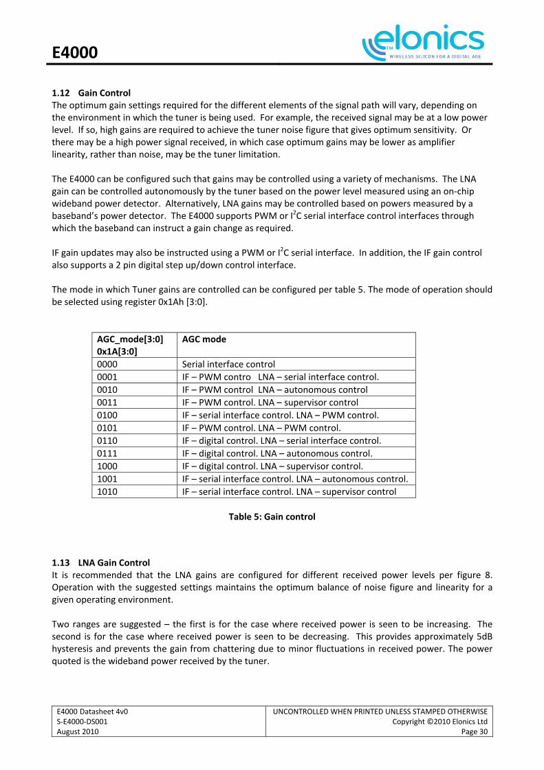
1.12 Gain Control The optimum gain settings required for the different elements of the signal path will vary, depending on the environment in which the tuner is being used. For example, the received signal may be at a low power level. If so, high gains are required to achieve the tuner noise figure that gives optimum sensitivity. Or there may be a high power signal received, in which case optimum gains may be lower as amplifier linearity, rather than noise, may be the tuner limitation. The E4000 can be configured such that gains may be controlled using a variety of mechanisms. The LNA gain can be controlled autonomously by the tuner based on the power level measured using an on‐chip wideband power detector. Alternatively, LNA gains may be controlled based on powers measured by a baseband’s power detector. The E4000 supports PWM or I2C serial interface control interfaces through which the baseband can instruct a gain change as required. IF gain updates may also be instructed using a PWM or I2C serial interface. In addition, the IF gain control also supports a 2 pin digital step up/down control interface. The mode in which Tuner gains are controlled can be configured per table 5. The mode of operation should be selected using register 0x1Ah [3:0].
AGC_mode[3:0] 0x1A[3:0]
AGC mode
0000 Serial interface control
0001 IF – PWM contro LNA – serial interface control.
0010 IF – PWM control LNA – autonomous control
0011 IF – PWM control. LNA – supervisor control
0100 IF – serial interface control. LNA – PWM control.
0101 IF – PWM control. LNA – PWM control.
0110 IF – digital control. LNA – serial interface control.
0111 IF – digital control. LNA – autonomous control.
1000 IF – digital control. LNA – supervisor control.
1001 IF – serial interface control. LNA – autonomous control.
1010 IF – serial interface control. LNA – supervisor control
Table 5: Gain control
1.13 LNA Gain Control It is recommended that the LNA gains are configured for different received power levels per figure 8. Operation with the suggested settings maintains the optimum balance of noise figure and linearity for a given operating environment. Two ranges are suggested – the first is for the case where received power is seen to be increasing. The second is for the case where received power is seen to be decreasing. This provides approximately 5dB hysteresis and prevents the gain from chattering due to minor fluctuations in received power. The power quoted is the wideband power received by the tuner.

E4000
E4000 Datasheet 4v0 S‐E4000‐DS001 August 2010
UNCONTROLLED WHEN PRINTED UNLESS STAMPED OTHERWISECopyright ©2010 Elonics Ltd
Page 31
Figure 8: LNA gain control
When using autonomous or supervisor modes, the RF gain control will automatically follow this profile. LNA gain step size is approximately 2.5dB. If desired, the user can instruct a larger step size to be used (5dB). This is controlled by register 0x20 [5].
1.13.1 LNA ‐ Serial Interface Gain Control
The LNA gain can be controlled using register writes via the serial interface. Gains are configured as per table 6.
Table 6: LNA – serial interface control
LNA Gain thresholds
10-
5-
0
5
10
15
20
25
30
35
-50 -40 -30 -20 -10
Input Power (dBm)
LN
A G
ain
(d
B)
Increasing power
Decreasing power
LNA gain 0x14h [3:0]
LNA gain(dB) (typical)
00X0 ‐5
00X1 ‐2.5
0100 0
0101 2.5
0110 5
0111 7.5
1000 10
1001 12.5
1010 15
1011 17.5
1100 20
1101 25
111X 30
E4000
E4000 Datasheet 4v0 S‐E4000‐DS001 August 2010
UNCONTROLLED WHEN PRINTED UNLESS STAMPED OTHERWISECopyright ©2010 Elonics Ltd
Page 32
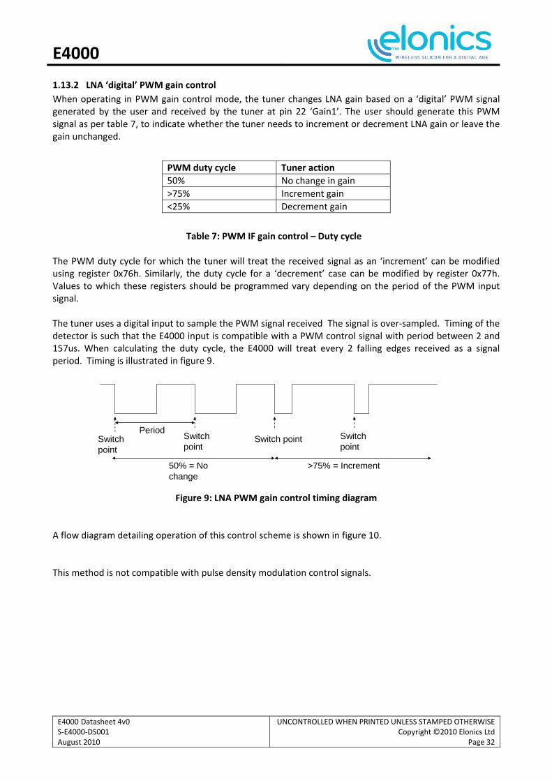
1.13.2 LNA ‘digital’ PWM gain control
When operating in PWM gain control mode, the tuner changes LNA gain based on a ‘digital’ PWM signal generated by the user and received by the tuner at pin 22 ‘Gain1’. The user should generate this PWM signal as per table 7, to indicate whether the tuner needs to increment or decrement LNA gain or leave the gain unchanged. Table 7: PWM IF gain control – Duty cycle The PWM duty cycle for which the tuner will treat the received signal as an ‘increment’ can be modified using register 0x76h. Similarly, the duty cycle for a ‘decrement’ case can be modified by register 0x77h. Values to which these registers should be programmed vary depending on the period of the PWM input signal. The tuner uses a digital input to sample the PWM signal received The signal is over‐sampled. Timing of the detector is such that the E4000 input is compatible with a PWM control signal with period between 2 and 157us. When calculating the duty cycle, the E4000 will treat every 2 falling edges received as a signal period. Timing is illustrated in figure 9.
Figure 9: LNA PWM gain control timing diagram A flow diagram detailing operation of this control scheme is shown in figure 10. This method is not compatible with pulse density modulation control signals.
PWM duty cycle Tuner action
50% No change in gain
>75% Increment gain
<25% Decrement gain
PeriodSwitch pointSwitch
point
>75% = Increment 50% = No change
Switch point
Switch point

E4000
E4000 Datasheet 4v0 S‐E4000‐DS001 August 2010
UNCONTROLLED WHEN PRINTED UNLESS STAMPED OTHERWISECopyright ©2010 Elonics Ltd
Page 33
Figure 10: LNA PWM gain control – flow diagram
1.13.3 LNA Autonomous Gain Control
The tuner is capable of determining when the LNA gain needs to be changed and modifying this gain such that optimal operation is maintained. An on‐chip wideband power detector measures the signal amplitude received by the tuner (in the bandwidth 64 – 1700MHz). The detector will measure average received signal power over a period of time per table 8. If the value is above or below the threshold levels set in registers 0x1Dh and 0x1Eh, then the gain will be updated When changing gains, the control loop will step sequentially through the possible settings until the desired signal level is reached.
Register 0x1F [3:0] AGC control loop update rate (us)
0000 60
0001 120
0010 240
0011 480
0100 960
0101 1920
0110 3840
0111 7680
1000 15360
1001 30720
1010 61440
Table 8: AGC control loop update rate
1.13.4 LNA Supervisor Gain Control
In supervisor mode, the LNA control loop operates as per 1.13.3 ‘LNA autonomous control’. However, the control loop will not update gains until instructed to by the user. The E4000 will indicate whether a LNA gain change is required by setting register 0x1Ah [7 or 6] = 1. If a gain change is required, the user should write 0x1Ah [5] = 1 which will instruct the loop to update gain.

E4000
E4000 Datasheet 4v0 S‐E4000‐DS001 August 2010
UNCONTROLLED WHEN PRINTED UNLESS STAMPED OTHERWISECopyright ©2010 Elonics Ltd
Page 34
1.14 Received Signal Strength Indicator (RSSI) The received signal strength measured by the tuner can be observed by the user through register 0x1Ch. The RSSI will function across a range of input powers (‐50 to ‐10dBm). This is the range of input powers over which the LNA gain should be modified to maintain linearity. For received powers lower than this the LNA should be set to maximum gain. The RSSI indicator can be accessed when operating in autonomous or supervisor gain control mode but not when using PWM or serial interface control. The RSSI register is scaled vs. received power as per figure 11.
Figure 11: RSSI detector register value vs. detector input power Note: The power shown in figu e 11 is the RMS input power to the RSSI detector. This relates to the E4000 input power per the formula‐
E4000 input power = RSSI detector power – LNA gain
1.15 Mixer Gain Control
1.15.1 Mixer Gain – Serial Interface Control
The Mixer may be controlled using register writes via the serial interface. Gains are set as per table 9. The mixer gain should be set high when a low signal level is received (<~ ‐35dBm) and set low when a high signal level is received at the input to the tuner (> ~ ‐35dBm). The E4000 received power can be monitored using the RSSI indicator
Table 9: Mixer gain control
Mixer gain 0x15h [0]
Mixer gain(dB) (typical)
0 4
1 12

E4000
E4000 Datasheet 4v0 S‐E4000‐DS001 August 2010
UNCONTROLLED WHEN PRINTED UNLESS STAMPED OTHERWISECopyright ©2010 Elonics Ltd
Page 35
1.15.2 Mixer Gain – Autonomous Control
The Mixer may be configured such that a gain change occurs automatically as the LNA gain is changed. This feature is enabled by setting 0x20h [0] = 1. Register 0x20h [4:1] should be programmed with the desired threshold value for which the user wishes mixer gain to change. This threshold corresponds to a LNA gain value as shown in table 6. It is recommended that the user configures 0x20h = 0x15h. This would mean that the mixer gain switches state when LNA gain is set to 7.5dB. For higher LNA gains, Mixer gain = 12dB. For 7.5dB or lower gains, Mixer gain = 4dB. Since the LNA gain control includes Hysteresis, the mixer gain will not toggle around a point due to small fluctuations in input power.
1.16 LNA Gain enhancement
It is recommended that register 0x24h is written = 5 on initialization of the tuner. This will enable the LNA gain enhancement mode. This is an automated control feature that will ncrease the NA gain by an additional 5dB when LNA and mixer are set to maximum gain levels. This mode s intended to optimize tuner noise figure in cases where gain is high, (small signals are rece ved). The LNA gain numbers quoted throughout this document assume that this register is programmed to the recommended value.
1.17 IF Gain Control IF gains can be controlled using the methods described n sections 1.17.1 to 1.17.4.
1.17.1 IF gain – Linearity / Sensitivity Mode
In some circumstances it may be preferable to optimise the IF gains for noise (for optimum sensitivity) or linearity (large signal handling, such as in the presence of an adjacent channel interferer). The user can set whether the tuner optimises gains for optimum sensitivity or linearity using 0x1Ah [4]. The mode may be switched by the user based on the tuner’s received signal power (sensitivity mode <~‐60dBm) or based on the user detecting the presence on an adjacent channel interferer.
Table 10: IF gain control mode Alternatively, the tuner can be configured to automatically switch between sensitivity and linearity modes. This feature is controlled using register 0x21h. Bits 6 to 1 can be programmed to the tuner gain at which the user wishes the device to switch between linearity & sensitivity modes. For example, default setting = 45dB. When LNA + mixer + IF gain is <45dB, the tuner will operate in linearity mode. Some Hysteresis is included to prevent modes switching around due to small fluctuations in power. Automated control of this gain optimisation mode is enabled by setting 0x21h [0] = 1.
AGC ramp 0x1A 4]
IF gain mode
0 Linearity
1 Sensitivity

E4000
E4000 Datasheet 4v0 S‐E4000‐DS001 August 2010
UNCONTROLLED WHEN PRINTED UNLESS STAMPED OTHERWISECopyright ©2010 Elonics Ltd
Page 36
1.17.2 IF Gain – Serial Interface Control
Table 11: IF stage 1 gain control
Table 12: IF stage 2 gain control
Table 13: IF stage 3 gain control
Table 14: IF stage 4 gain control
Table 15: IF stage 5 gain control
IF stage 1 gain 0x16h [0]
IF stage 1 gain(dB) (typical)
0 ‐3
1 6
IF stage 2 gain 0x16h [2:1]
IF stage 2 gain(dB) (typical)
00 0
01 3
10 6
11 9
IF stage 3 gain 0x16h [4:3]
IF stage 3 gain(dB) (typical)
00 0
01 3
10 6
11 9
IF stage 4 gain 0x16h [6:5]
IF stage 4 gain(dB) (typical)
00 0
01 1
1x 2
IF stage 5 gain 0x17h [2:0]
IF stage 5 gain(dB) (typical)
000 3
001 6
010 9
011 12
1xx 15

E4000
E4000 Datasheet 4v0 S‐E4000‐DS001 August 2010
UNCONTROLLED WHEN PRINTED UNLESS STAMPED OTHERWISECopyright ©2010 Elonics Ltd
Page 37
Table 16: IF stage 6 gain control
IF stage 6 gain 0x17h [5:3]
IF stage 6 gain(dB) (typical)
000 3
001 6
010 9
011 12
1xx 15

E4000
E4000 Datasheet 4v0 S‐E4000‐DS001 August 2010
UNCONTROLLED WHEN PRINTED UNLESS STAMPED OTHERWISECopyright ©2010 Elonics Ltd
Page 38
Linearity Mode
Register 0x16h Register 0x17h IF Stage 1 IF Stage 2 IF Stage 3 IF Stage 4 IF Stage 5 IF Stage 6 Total Gain (dB)
0x7f 0x24 9 9 9 3 15 15 60
0x5f 0x24 9 9 9 2 15 15 59
0x3f 0x24 9 9 9 1 15 15 58
0x1f 0x24 9 9 9 0 15 15 57
0x5d 0x24 9 6 9 2 15 15 56
0x3d 0x24 9 6 9 1 15 15 55
0x1d 0x24 9 6 9 0 15 15 54
0x5b 0x24 9 3 9 2 15 15 53
0x3b 0x24 9 3 9 1 15 15 52
0x1b 0x24 9 3 9 0 15 15 51
0x59 0x24 9 0 9 2 15 15 50
0x39 0x24 9 0 9 1 15 15 49
0x19 0x24 9 0 9 0 15 15 48
0x5c 0x24 0 6 9 2 15 15 47
0x3c 0x24 0 6 9 1 15 15 46
0x1c 0x24 0 6 9 0 15 15 45
0x5a 0x24 0 3 9 2 15 15 44
0x3a 0x24 0 3 9 1 15 15 43
0x1a 0x24 0 3 9 0 15 15 42
0x58 0x24 0 0 9 2 15 15 41
0x38 0x24 0 0 9 1 15 15 40
0x18 0x24 0 0 9 0 15 15 39
0x50 0x24 0 0 6 2 15 15 38
0x30 0x24 0 0 6 1 15 15 37
0x10 0x24 0 0 6 0 15 15 36
0x48 0x24 0 0 3 2 15 15 35
0x28 0x24 0 0 3 1 15 15 34
0x08 0x24 0 0 3 0 15 15 33
0x40 0x24 0 0 0 2 15 15 32
0x20 0x24 0 0 0 1 15 15 31
0x00 0x24 0 0 0 0 15 15 30
0x40 0x23 0 0 0 2 12 15 29
0x20 0x23 0 0 0 1 12 15 28
0x00 0x23 0 0 0 0 12 15 27
0x40 0x22 0 0 0 2 9 15 26
0x20 0x22 0 0 0 1 9 15 25
0x00 0x22 0 0 0 0 9 15 24
0x40 0x21 0 0 0 2 6 15 23
0x20 0x21 0 0 0 1 6 15 22
0x00 0x21 0 0 0 0 6 15 21
0x40 0x20 0 0 0 2 3 15 20
0x20 0x20 0 0 0 1 3 15 19
0x00 0x20 0 0 0 0 3 15 18
0x40 0x18 0 0 0 2 3 12 17
0x20 0x18 0 0 0 1 3 12 16
0x00 0x18 0 0 0 0 3 12 15
0x40 0x10 0 0 0 2 3 9 14
0x20 0x10 0 0 0 1 3 9 13
0x00 0x10 0 0 0 0 3 9 12
0x40 0x08 0 0 0 2 3 6 11
0x20 0x08 0 0 0 1 3 6 10
0x00 0x08 0 0 0 0 3 6 9
0x40 0x00 0 0 0 2 3 3 8
0x20 0x00 0 0 0 1 3 3 7
0x00 0x00 0 0 0 0 3 3 6
E4000
E4000 Datasheet 4v0 S‐E4000‐DS001 August 2010
UNCONTROLLED WHEN PRINTED UNLESS STAMPED OTHERWISECopyright ©2010 Elonics Ltd
Page 39
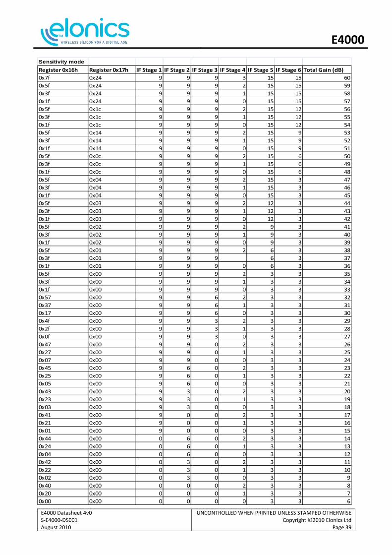
Sensitivity mode
Register 0x16h Register 0x17h IF Stage 1 IF Stage 2 IF Stage 3 IF Stage 4 IF Stage 5 IF Stage 6 Total Gain (dB)
0x7f 0x24 9 9 9 3 15 15 60
0x5f 0x24 9 9 9 2 15 15 59
0x3f 0x24 9 9 9 1 15 15 58
0x1f 0x24 9 9 9 0 15 15 57
0x5f 0x1c 9 9 9 2 15 12 56
0x3f 0x1c 9 9 9 1 15 12 55
0x1f 0x1c 9 9 9 0 15 12 54
0x5f 0x14 9 9 9 2 15 9 53
0x3f 0x14 9 9 9 1 15 9 52
0x1f 0x14 9 9 9 0 15 9 51
0x5f 0x0c 9 9 9 2 15 6 50
0x3f 0x0c 9 9 9 1 15 6 49
0x1f 0x0c 9 9 9 0 15 6 48
0x5f 0x04 9 9 9 2 15 3 47
0x3f 0x04 9 9 9 1 15 3 46
0x1f 0x04 9 9 9 0 15 3 45
0x5f 0x03 9 9 9 2 12 3 44
0x3f 0x03 9 9 9 1 12 3 43
0x1f 0x03 9 9 9 0 12 3 42
0x5f 0x02 9 9 9 2 9 3 41
0x3f 0x02 9 9 9 1 9 3 40
0x1f 0x02 9 9 9 0 9 3 39
0x5f 0x01 9 9 9 2 6 3 38
0x3f 0x01 9 9 9 6 3 37
0x1f 0x01 9 9 9 0 6 3 36
0x5f 0x00 9 9 9 2 3 3 35
0x3f 0x00 9 9 9 1 3 3 34
0x1f 0x00 9 9 9 0 3 3 33
0x57 0x00 9 9 6 2 3 3 32
0x37 0x00 9 9 6 1 3 3 31
0x17 0x00 9 9 6 0 3 3 30
0x4f 0x00 9 9 3 2 3 3 29
0x2f 0x00 9 9 3 1 3 3 28
0x0f 0x00 9 9 3 0 3 3 27
0x47 0x00 9 9 0 2 3 3 26
0x27 0x00 9 9 0 1 3 3 25
0x07 0x00 9 9 0 0 3 3 24
0x45 0x00 9 6 0 2 3 3 23
0x25 0x00 9 6 0 1 3 3 22
0x05 0x00 9 6 0 0 3 3 21
0x43 0x00 9 3 0 2 3 3 20
0x23 0x00 9 3 0 1 3 3 19
0x03 0x00 9 3 0 0 3 3 18
0x41 0x00 9 0 0 2 3 3 17
0x21 0x00 9 0 0 1 3 3 16
0x01 0x00 9 0 0 0 3 3 15
0x44 0x00 0 6 0 2 3 3 14
0x24 0x00 0 6 0 1 3 3 13
0x04 0x00 0 6 0 0 3 3 12
0x42 0x00 0 3 0 2 3 3 11
0x22 0x00 0 3 0 1 3 3 10
0x02 0x00 0 3 0 0 3 3 9
0x40 0x00 0 0 0 2 3 3 8
0x20 0x00 0 0 0 1 3 3 7
0x00 0x00 0 0 0 0 3 3 6
E4000
E4000 Datasheet 4v0 S‐E4000‐DS001 August 2010
UNCONTROLLED WHEN PRINTED UNLESS STAMPED OTHERWISECopyright ©2010 Elonics Ltd
Page 40
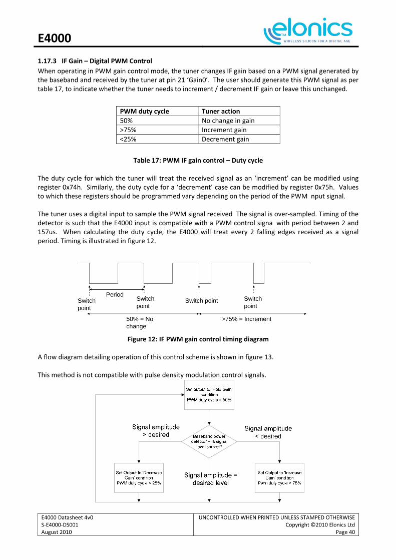
1.17.3 IF Gain – Digital PWM Control
When operating in PWM gain control mode, the tuner changes IF gain based on a PWM signal generated by the baseband and received by the tuner at pin 21 ‘Gain0’. The user should generate this PWM signal as per table 17, to indicate whether the tuner needs to increment / decrement IF gain or leave this unchanged.
Table 17: PWM IF gain control – Duty cycle The duty cycle for which the tuner will treat the received signal as an ‘increment’ can be modified using register 0x74h. Similarly, the duty cycle for a ‘decrement’ case can be modified by register 0x75h. Values to which these registers should be programmed vary depending on the period of the PWM nput signal. The tuner uses a digital input to sample the PWM signal received The signal is over‐sampled. Timing of the detector is such that the E4000 input is compatible with a PWM control signa with period between 2 and 157us. When calculating the duty cycle, the E4000 will treat every 2 falling edges received as a signal period. Timing is illustrated in figure 12.
Figure 12: IF PWM gain control timing diagram A flow diagram detailing operation of this control scheme is shown in figure 13. This method is not compatible with pulse density modulation control signals.
PWM duty cycle Tuner action
50% No change in gain
>75% Increment gain
<25% Decrement gain
PeriodSwitch pointSwitch
point
>75% = Increment 50% = No change
Switch point
Switch point

E4000
E4000 Datasheet 4v0 S‐E4000‐DS001 August 2010
UNCONTROLLED WHEN PRINTED UNLESS STAMPED OTHERWISECopyright ©2010 Elonics Ltd
Page 41
Figure 13: IF PWM gain control – flow diagram
1.17.4 IF Gain – Digital Control
It is possible to control IF gain using a 2 pin digital control interface. The gain is changed depending on the state of Pins 21 ‘Gain0’ and 22 ‘gain1’. Gains are incremented or decremented in steps of 1dB. The default truth table is shown in Table 18.
Digital control ‘Gain 1 / Gain 0’
Tuner action
00 Decrease gain
01 Hold gain
10 Hold gain
11 Increase gain
Table 18: IF gain – digital interface control
An alternative logic scheme is provided. This logic can be can be selected by setting 0x86h = 0x51h. A truth table is shown in table 19.
Digital control ‘Gain 1 / Gain 0’
Tuner action
00 Hold gain
01 Increase gain
10 Decrease gain
11 Hold gain
Table 19: IF gain – digital interface control
Figure 14 details the flow diagram that should be followed when using this gain control interface.
Figure 14: Digital up/down gain control interface – flow diagram

E4000
E4000 Datasheet 4v0 S‐E4000‐DS001 August 2010
UNCONTROLLED WHEN PRINTED UNLESS STAMPED OTHERWISECopyright ©2010 Elonics Ltd
Page 42
Note: A ‘no change’ condition must be sent between sequential increment or sequential decrement commands. Each state should be maintained for > 130ns in order for the E4000 to sample levels and instruct a gain change.
1.18 Output Common Mode Voltage The common mode output voltage of the tuner defaults to 0.58V. It is possible to increase this DC voltage level as per table 20.
Register 0x2Fh [2:0] Common mode voltage (mV)
000 580
001 650
010 650
011 700
100 850
101 900
110 900
111 950
Table 20: Output common mode voltage
It may be possible to programme the tuner output common mode voltage level to match the Baseband ADC common mode voltage level, eliminating the requirement for DC blocking capacitors. If this feature is used it should be noted that tuner linear ty may degrade as common mode voltage is increased. It should also be noted that in some circumstances, voltages may vary by up to +/‐160mV vs. nominal value, (due to a combination of process / temperature variation and tuner DC offsets). If DC blocking capacitors are removed, the baseband ADC would be required to tolerate this variation.
E4000
E4000 Datasheet 4v0 S‐E4000‐DS001 August 2010
UNCONTROLLED WHEN PRINTED UNLESS STAMPED OTHERWISECopyright ©2010 Elonics Ltd
Page 43
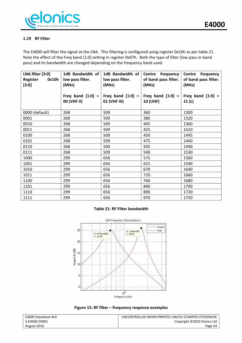
1.19 RF Filter
The E4000 will filter the signal at the LNA. This filtering is configured using register 0x10h as per table 21. Note the effect of the Freq band [1:0] setting in register 0x07h. Both the type of filter (low pass or band pass) and its bandwidth are changed depending on the frequency band used.
LNA filter [3:0] Register 0x10h [3:0]
1dB Bandwidth of low pass filter. (MHz) Freq band [1:0] = 00 (VHF II)
1dB Bandwidth of low pass filter. (MHz) Freq band [1:0] = 01 (VHF III)
Centre frequency of band pass filter. (MHz) Freq band [1:0] = 10 (UHF)
Centre frequency of band pass filter. (MHz) Freq band [1:0] = 11 (L)
0000 (default) 268 509 360 1300
0001 268 509 380 1320
0010 268 509 405 1360
0011 268 509 425 1410
0100 268 509 450 1445
0101 268 509 475 1460
0110 268 509 505 1490
0111 268 509 540 1530
1000 299 656 575 1560
1001 299 656 615 1590
1010 299 656 670 1640
1011 299 656 720 1660
1100 299 656 760 1680
1101 299 656 840 1700
1110 299 656 890 1720
1111 299 656 970 1750
Table 21: RF Filter bandwidth
Figure 15: RF filter – frequency response examples

E4000
E4000 Datasheet 4v0 S‐E4000‐DS001 August 2010
UNCONTROLLED WHEN PRINTED UNLESS STAMPED OTHERWISECopyright ©2010 Elonics Ltd
Page 44
1.20 IF Filter
The IF path contains 3 filtering sections that are used to attenuate adjacent channel interferers and provide anti‐alias filtering such that high frequencies are eliminated. Optimum filter settings will vary depending on the channel bandwidth, adjacent channel interferer size, ADC sampling speed and ADC anti‐alias filter response.
1.21 Mixer Filter
This filter section is located between the mixer and 1st IF gain stage. Filter attenuation is configured as per table 22 and figure 16.
Table 22: Mixer filter settings
Figure 16: Mixer filter settings
Reg 0x11h[7:4] 0.2dB Bandwidth
0xxx 27
1000 4.6
1001 4.2
1010 3.8
1011 3.4
1100 3
1101 2.7
1110 2 3
1111 1.9
E4000
E4000 Datasheet 4v0 S‐E4000‐DS001 August 2010
UNCONTROLLED WHEN PRINTED UNLESS STAMPED OTHERWISECopyright ©2010 Elonics Ltd
Page 45
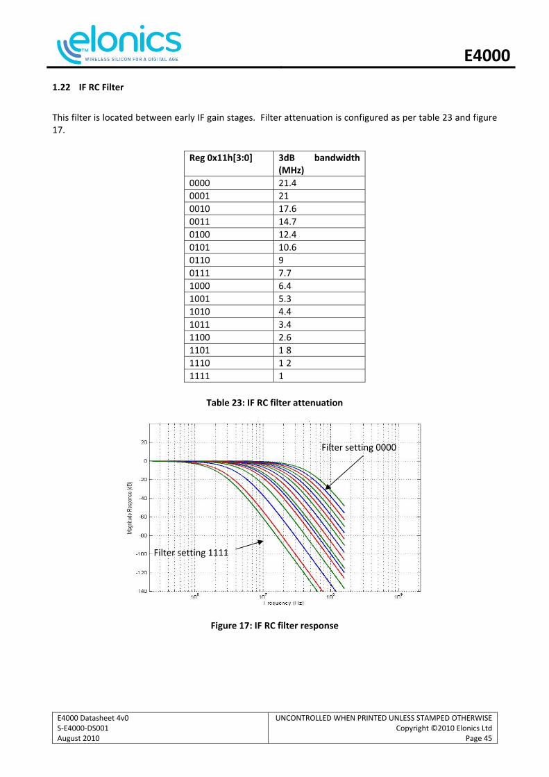
1.22 IF RC Filter
This filter is located between early IF gain stages. Filter attenuation is configured as per table 23 and figure 17.
Table 23: IF RC filter attenuation
Figure 17: IF RC filter response
Reg 0x11h[3:0] 3dB bandwidth (MHz)
0000 21.4
0001 21
0010 17.6
0011 14.7
0100 12.4
0101 10.6
0110 9
0111 7.7
1000 6.4
1001 5.3
1010 4.4
1011 3.4
1100 2.6
1101 1 8
1110 1 2
1111 1
Filter setting 1111
Filter setting 0000

E4000
E4000 Datasheet 4v0 S‐E4000‐DS001 August 2010
UNCONTROLLED WHEN PRINTED UNLESS STAMPED OTHERWISECopyright ©2010 Elonics Ltd
Page 46
1.23 IF Channel Filter
The channel filter is a sharp roll off filter, attenuating adjacent channel interferers. Response is as per table 24 and figure 18.
IF channel filter setting Register 0x12h [4:0]
Filter corner frequency (MHz)
IF channel filter setting Register 0x12h [4:0]
Filter corner frequency (MHz)
00000 5.5 10000 3
00001 5.3 10001 2.95
00010 5 10010 2.9
00011 4.8 10011 2.8
00100 4.6 10100 2 75
00101 4.4 10101 2.7
00110 4.3 10110 2.6
00111 4.1 10111 2.55
01000 3.9 11000 2.5
01001 3.8 11001 2.45
01010 3.7 11010 2 4
01011 3.6 11011 2.3
01100 3.4 11100 2.28
01101 3.3 11101 2.24
01110 3.2 11110 2.2
01111 3.1 11111 2.15
Table 24: IF channel filter
Figure 18: IF channel filter response The channel filter’s corner frequency may vary slightly from chip to chip. The E4000 contains a calibration feature by which the user can optimise the channel filter setting. To instruct a filter calibration the user should write register 0x7Bh [0] = 1. The calibration will calculate a value based on frequency error vs. nominal corner frequency. This is stored in register 0x7Bh [6:1]. Scaling is as per figure 19. For example, when using a 26MHz reference clock a value of 45 is observed. This indicates that filter corner frequency is 10% lower than nominal value in table 24. The user can select the optimum filter
Setting 00000
Setting 11111
Filter responses for settings 11111, 10111, 01111, 01011, 00111, 00000 are illustrated

E4000
E4000 Datasheet 4v0 S‐E4000‐DS001 August 2010
UNCONTROLLED WHEN PRINTED UNLESS STAMPED OTHERWISECopyright ©2010 Elonics Ltd
Page 47
setting based on this value. If a corner frequency of 3.9MHz is desired, the optimum setting would be the 4.3MHz (nominal) filter setting (4.3MHz nominal ‐ 10% = 3.87MHz actual). Calibration value vs. filter scaling required is shown in figure 19. Alternatively the formula below can be used to calculate the filter scaling required.
Percentage error = 100 ‐ (64 x RC filter cal value / Reference clock frequency (MHz))
Figure 19: Filter calibration If desired it is possible for the user not to use the filter calibration. If so, it is recommended that the filter corner frequency is set 350kHz above the wanted band edge.
Filter calibration
-200
-150
-100
-50
0
50
100
150
0 20 40 60 80
RC filter value
Fil
ter
% e
rro
r clock =16MHz
clock =26MHz
clock =32MHz
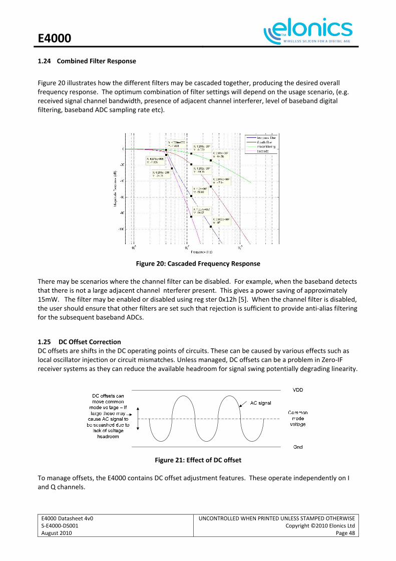
E4000
E4000 Datasheet 4v0 S‐E4000‐DS001 August 2010
UNCONTROLLED WHEN PRINTED UNLESS STAMPED OTHERWISECopyright ©2010 Elonics Ltd
Page 48
1.24 Combined Filter Response
Figure 20 illustrates how the different filters may be cascaded together, producing the desired overall frequency response. The optimum combination of filter settings will depend on the usage scenario, (e.g. received signal channel bandwidth, presence of adjacent channel interferer, level of baseband digital filtering, baseband ADC sampling rate etc).
Figure 20: Cascaded Frequency Response
There may be scenarios where the channel filter can be disabled. For example, when the baseband detects that there is not a large adjacent channel nterferer present. This gives a power saving of approximately 15mW. The filter may be enabled or disabled using reg ster 0x12h [5]. When the channel filter is disabled, the user should ensure that other filters are set such that rejection is sufficient to provide anti‐alias filtering for the subsequent baseband ADCs.
1.25 DC Offset Correction DC offsets are shifts in the DC operating points of circuits. These can be caused by various effects such as local oscillator injection or circuit mismatches. Unless managed, DC offsets can be a problem in Zero‐IF receiver systems as they can reduce the available headroom for signal swing potentially degrading linearity.
Figure 21: Effect of DC offset
To manage offsets, the E4000 contains DC offset adjustment features. These operate independently on I and Q channels.

E4000
E4000 Datasheet 4v0 S‐E4000‐DS001 August 2010
UNCONTROLLED WHEN PRINTED UNLESS STAMPED OTHERWISECopyright ©2010 Elonics Ltd
Page 49
1.26 DC Offset Control There are three mechanisms for DC offset control; an initial calibration, a look‐up table and a time varying tracking of DC offset. These mechanisms are described in sections 0 to1.27.2. The DC offset is dependent on the device and on the frequency of operation. The E4000 will perform a calibration routine in order to reduce offsets to a low level. This routine is performed after a reset or can be instructed to run by the user. Register 0x29h [0] should be set =1 to request a DC offset calibration. Note 1: The DC range detector should be left enabled when performing this calibration (default setting). (Register 0x2Dh [2]). It is also possible to set DC offset manually. The resolution of I and Q channel offset controls are set using register 0x2Ch. ‘High resolution’ gives very fine voltage steps vs. ‘low’ resolution (for maximum tuner gain ~ 40mV vs. 300mV step size) but does not cover as large a voltage range. The highest resolution setting that works for a given device is recommended as this will give most accurate control. The offset itself may be programmed using registers 0x2Ah and 0x2Bh.
1.27 Dynamic DC Offset Correction The E4000 gain will be changed as received input powers vary This can result in DC offsets changing. The E4000 has two methods of dynamic tracking to compensate for this change. For fastest tracking of DC offsets it is recommended that both the look‐up table (1.27.1) and time varying DC offset compensation (1.27.2) are used. The look‐up table moves DC offset to approximately the correct level while the time varying compensation subsequently fine tunes to reach the optimum level.
1.27.1 Look‐Up table
The first method of dynamic tracking is to program and use the look‐up tables in registers 0x50h to 0x53h and 0x60h to 0x63h. The DC offset will be changed to the values stored in these registers as mixer and IF stage 0 gains are varied. This compensates for any variation seen in DC offset as gains are changed. Look‐up tables are enabled as default (register 0x2Dh [1:0]). If this method is not used, this feature should be disabled. The naming convention for the registers is such that the first number refers to the mixer gain set in register 0x15h [0] The next number refers to IF stage 1 gain which is set by register 0x16h [0]. I.e. DC offset Q–00 stores the value that will compensate for Q channel DC offset and will be automatically entered into register 0x2Bh [5:0] when gains are changed such that 0x15h [0] = 0 and 0x16h [0] = 0. Similarly Qrange–00 refers to the Q range setting set in register 0x2C [5:4]. If the look‐up table feature is enabled, the user should populate the table as part of the tuner initialisation. The user must cycle through each combined gain setting of the mixer and IF gain stage 1. The mixer gain is set in register 0x15h [0] and IF stage 1 gain is set by register 0x16h [2:0]. A DC offset calibration should be instructed at each gain setting and the resulting values read. The values should then be programmed into the look up table. It is recommended that this initialization is performed with other IF gains set to maximum values.

E4000
E4000 Datasheet 4v0 S‐E4000‐DS001 August 2010
UNCONTROLLED WHEN PRINTED UNLESS STAMPED OTHERWISECopyright ©2010 Elonics Ltd
Page 50
1.27.2 Time Varying DC Offset Compensation
A further method of tracking time varying DC offset changes is to use the E4000’s DC offset monitor. This is enabled as per table 25.
Table 25: Time varying DC offset control
This monitor detects whether the DC offset goes above or below a threshold set by 0x72h [7:0]. If so, a control loop will increment or decrement the DC offset value until an acceptable level is reached. The control loop timing is set by register 0x73h [2:0]. Both registers should remain set at default values. If register 0x2Dh [3] is set = 1, this configures the time varying DC offset to allow the controller to increment DC offset range. If a minimum or maximum level of DC offset i reached, the DC offset range will be increased, allowing a larger range of offset tracking if required. A supervisory mode of operation is also provided in which the control loop runs as described above. However, the tuner will not change DC offset until instructed to by the user. If 0x70h [4 or 3] = 1, an I channel DC offset increment or decrement is required. Writing a value of 1 to 0x70h [2] will instruct the E4000 to perform this update. Similarly Q channel updates can be controlled using register 0x71h. It is recommended that time varying DC offset is used to ensure accurate correction of DC offsets.
Dynamic tracking mode
Dynamic DC offset I channel mode [1:0] 0x70h [1:0]
Dynamic DC offset Q channel mode [1:0] 0x71h [1:0]
Off 00 00
Auto (recommended) 01 01
Supervisor 10 10
Off 11 11
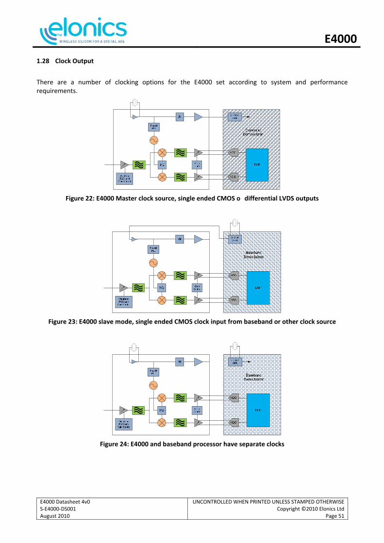
E4000
E4000 Datasheet 4v0 S‐E4000‐DS001 August 2010
UNCONTROLLED WHEN PRINTED UNLESS STAMPED OTHERWISECopyright ©2010 Elonics Ltd
Page 51
1.28 Clock Output
There are a number of clocking options for the E4000 set according to system and performance requirements.
Figure 22: E4000 Master clock source, single ended CMOS o differential LVDS outputs
Figure 23: E4000 slave mode, single ended CMOS clock input from baseband or other clock source
Figure 24: E4000 and baseband processor have separate clocks
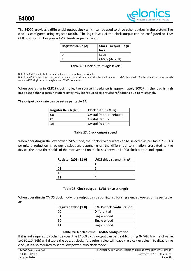
E4000
E4000 Datasheet 4v0 S‐E4000‐DS001 August 2010
UNCONTROLLED WHEN PRINTED UNLESS STAMPED OTHERWISECopyright ©2010 Elonics Ltd
Page 52
The E4000 provides a differential output clock which can be used to drive other devices in the system. The clock is configured using register 0x06h. The logic levels of the clock output can be configured to 1.5V CMOS or custom low power LVDS levels as per table 26.
Table 26: Clock output logic levels Note 1: In CMOS mode, both normal and inverted outputs are provided. Note 2: CMOS voltage levels are such that these can clock a baseband using the low power LVDS clock mode The baseband can subsequently switch to LVDS logic levels or single ended CMOS clock levels.
When operating in CMOS clock mode, the source impedance is approximately 1000R. If the load is high impedance then a termination resistor may be required to prevent reflections due to mismatch. The output clock rate can be set as per table 27.
Register 0x06h [4:3] Clock output (MHz)
00 Crystal freq ÷ 1 (default)
01 Crystal freq ÷ 2
10 Crystal freq ÷ 4
Table 27: Clock output speed
When operating in the low power LVDS mode, the clock driver current can be selected as per table 28. This permits a reduction in power dissipation, depending on the differential termination presented to the device, the input thresholds of the receiver and on the losses between E4000 clock output and input.
Table 28: Clock output – LVDS drive strength
When operating in CMOS clock mode, the output can be configured for single ended operation as per table 29
Table 29: Clock output – CMOS configuration If it is not required by other devices, the E4000 clock output can be disabled using 0x7Ah. A write of value 10010110 (96h) will disable the output clock. Any other value will leave the clock enabled. To disable the clock, it is also required to set to low power LVDS clock mode.
Register 0x06h [2] Clock output logic level
0 LVDS
1 CMOS (default)
Register 0x06h [1 0] LVDS drive strength (mA)
00 1
01 2
10 3
11 4
Register 0x06h [1:0] CMOS clock configuration
00 Differential
01 Single ended
10 Single ended
11 Single ended

E4000
E4000 Datasheet 4v0 S‐E4000‐DS001 August 2010
UNCONTROLLED WHEN PRINTED UNLESS STAMPED OTHERWISECopyright ©2010 Elonics Ltd
Page 53
Typically, the output clock will initialise 100μs after the tuner is powered on.
1.29 Clock Input
It is possible to generate the E4000 clock using an external device and to input the clock into pin 28 ‘CLOCKIN’. This is an alternative clock configuration mode to the on‐chip oscillator described in section 0. If a clock signal is present this will be detected by the E4000 and the on‐chip oscillator will be turned off. aThe input clock source must have a minimum DC voltage level of 0.7V. This pin will not tolerate 3.3V logic inputs. If it is desired to use a 3.3V logic signal to clock the tuner then a pot ntia divider should be connected externally to the tuner to reduce voltage swing. Clock input frequency should be within the range 16 to 30MHz. Clock input jitter should be <5ps RMS to avoid reduction in tuner performance.
1.30 Reset
In reset mode all registers are reset to their default conditions and all digital state machines initialised. The chip can be instructed to perform a reset using the I2C register 0x00h [0]. This register is self clearing. Also, the E4000 will monitor the supply voltage. If this drops be ow 0.8V for longer than 100ns, a reset will be applied automatically. Register 0x00h [2] contains a power on reset detector. The E4000 will set this to 1 after power up or after a reset occurs. Writing 1 to this bit causes the register to clear. This can subsequently be read to determine whether the tuner has undergone a reset.
E4000
E4000 Datasheet 4v0 S‐E4000‐DS001 August 2010
UNCONTROLLED WHEN PRINTED UNLESS STAMPED OTHERWISECopyright ©2010 Elonics Ltd
Page 54
1.31 Power Save Modes
1.31.1 Power Down Mode
The device enters power down mode under the control of the PDNB input (pin 14). In power down mode all the analogue circuits are disabled and clocks stopped. The clock outputs and Crystal oscillator pins do not function. The E4000 will be operational 20ms after the power down input goes high, Tinit_pd.
Figure 25: PDNB Start Up Timing
1.31.2 Standby Mode
The device enters standby mode under the control of the STBYB input (pin 13). Alternatively, this can be controlled using the I2C register 0x00h [1]. In standby mode much of the analogue circuitry is disabled. However, the clock output and serial interface are left running. After exiting s andby mode, the tuner will configure as it was set before the standby occurred. The standby mode is intended for time‐slicing use in DVB‐H applications The E4000 data path will be operationa 2ms after the STBYB input goes high, Tinit_stby.
Figure 26: STBYB Start Up Timing
STBYB
IVOUTP/N,
QVOUTP/N
t
v
Tinit_stby (2ms)
PDNB
IVOUTP/N,
QVOUTP/N
t
v
Tinit_pd

E4000
E4000 Datasheet 4v0 S‐E4000‐DS001 August 2010
UNCONTROLLED WHEN PRINTED UNLESS STAMPED OTHERWISECopyright ©2010 Elonics Ltd
Page 55
1.32 Initialisation
Pow
er a
pplie
d
Cry
stal
osc
illat
or e
nabl
edT
uner
out
put c
lock
av
alai
labl
e
I2 C c
omm
unic
atio
ns
enab
led
Fre
quen
cy
synt
hesi
zer
and
data
pa
th o
pera
tiona
l
Figure 27: Typical initialisation timeline
The tuner will typically take around 2ms from powe being applied to being fully operational. A clock output will typically be available after 100us. I2C communications are possible after 110us. Frequency synthesizer and data path operational is defined as he point where the E4000 initialisation is complete but does not include the user configuration of the tuner, (e.g. gain control). When supply domains are connected together no power supply sequencing is required. However, if a user decides to separate the tuner’s different supply domains, care should be taken with supply sequencing. AVDD should be present when PLL_VDD is turned on. IFVDD should be ramped after other supplies.

E4000
E4000 Datasheet 4v0 S‐E4000‐DS001 August 2010
UNCONTROLLED WHEN PRINTED UNLESS STAMPED OTHERWISECopyright ©2010 Elonics Ltd
Page 56
APPLICATION INFORMATION
CLOCK N
RFIN_1RF
NPUT
C4
100pF
GAIN0
GAIN1
AGCCONTROL
INPUTS
A0
A1
I2C ADDRESS
ELECT
STBYB
5RFIN_1
21
22
GA N0
GA N1
1
12
13STBYB
A0
A1
TUNER AVDD (+1.5V)
28
29XTAL
CLOCK N
26
27
25
TUN_DGND0
TUN_DGND1
TUN_DVDD
2
3
VBG
REXT
IVOUTP
IVOUTN
IF OUTPUTS
C9
C800nF
100nF
20
19
IVOUTP
IVOUTN
QVOUTP
QVOUTN
C7
C6100nF
100nF
18
17
QVOUTP
QVOUTN
AGND0
LNAGND2
LNAGND
FGND
PLL_GND
1
7
6
30
10
FIT OPTION
LNAVDD8
IFVDD
PLL_VDD9
31
L2100nH
TUNER DVDD (+1 5V)
L6100nH
L3100nH
C10100pF
C110nF
R110k
C3
100pF
AVDD32
IMPORTANT NOTES1. E4000 metal paddle (bottom of package) should be connected to TUNER GROUND2. Pins 4, 6, 7 should be connected to a common LNAGND plane, separate from the tuner ground plane3. C6,7,8,9 Optional dependent on ability to match output common mode voltage to input common mode voltage of baseband demodulator input
C12
100pF
C2
100nF
SDAT
SCLK
MICRO CONTROL
I/F
15
16
SDAT
SCLK
PDNB14
PDNBHARDWARE
CONTROL I/F
CKOUTP24
CKOUTP
CKOUTN23
CKOUTN
RFSHIELD4
C5
100pF
C11
100pF
L5100nH
L1100nH
CONNECT TO LNAGND
Tuner Ground
Tuner Ground
Tuner Ground
L4100nH
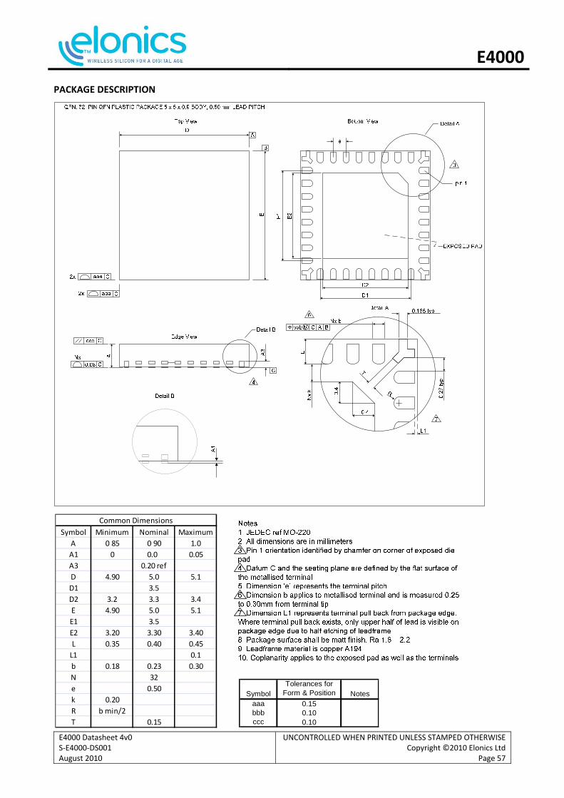
E4000
E4000 Datasheet 4v0 S‐E4000‐DS001 August 2010
UNCONTROLLED WHEN PRINTED UNLESS STAMPED OTHERWISECopyright ©2010 Elonics Ltd
Page 57
PACKAGE DESCRIPTION
Symbol Minimum Nominal Maximum
A 0 85 0 90 1.0
A1 0 0.0 0.05
A3 0.20 ref
D 4.90 5.0 5.1
D1 3.5
D2 3.2 3.3 3.4
E 4.90 5.0 5.1
E1 3.5
E2 3.20 3.30 3.40
L 0.35 0.40 0.45
L1 0.1
b 0.18 0.23 0.30
N 32
e 0.50
k 0.20
R b min/2
T 0.15
Common Dimensions
SymbolTolerances for
Form & Position Notesaaa 0.15bbb 0.10ccc 0.10

E4000
E4000 Datasheet 4v0 S‐E4000‐DS001 August 2010
UNCONTROLLED WHEN PRINTED UNLESS STAMPED OTHERWISECopyright ©2010 Elonics Ltd
Page 58
REVISION HISTORY
Date Release Description of Changes Changed Pages
10 Dec 08 1v0 Preliminary technical release
26 Mar 09 2v0 Updated parametric data
21 Jan 10 2v1 Updated external package and component diagram
27 Jan 10 2v2 Part number updated with dry pack option 5
27 April 10 3v0 Updated to pre‐production status, updated component diagram
26 May 10 3v1 Updated pin names
19 August 10
4v0 Updated to Production release status

E4000
E4000 Datasheet 4v0 S‐E4000‐DS001 August 2010
UNCONTROLLED WHEN PRINTED UNLESS STAMPED OTHERWISECopyright ©2010 Elonics Ltd
Page 59
LEGAL NOTICES
Product information is current as of publication date. Elonics Ltd (“Elonics”) products and services are sold subject to Elonics’ terms and conditions of sale, delivery and payment supplied at the time of order acknowledgement. Elonics warrants performance of its products to the specifications in effect at the date of shipment. Elonics reserves the right to make changes to its products and specifications or to discontinue any product or service without notice. Customers should therefore obtain the latest version of relevant information from Elonics to verify that the information is current. Testing and other quality control techniques are utilised to the extent Elonics deems necessary to support its warranty. Specific testing of all parameters of each device is not necessarily performed unless required by law or regulation. In order to minimise risks associated with customer applications, the customer must use adequate design and operating safeguards to minimise inherent or procedural hazards. Elonics is not liable for applications assistance or customer product design. The customer is solely responsible for its selection and use of Elonics products. Elonics is not liable for such selection or use nor for use of any circuitry other than circuitry entirely embodied in a Elonics product. Elonics produ ts are not intended for use in life support systems, appliances, nuclear systems or systems where malfunction can reasonably be expected to result in personal injury, death or severe property or environmental damage. Any use of products by the customer for such purposes is at the customer’s own risk. Elonics does not grant any licence (express or implied) under any patent right, copyright, mask work right or other intellectual property right of Elonics covering or relating to any combination, machine, or process in which its products or services might be or are used. Any provision or publication of any third party’s products or services does not constitute Elonics approval, licence, warranty or endorsement thereof. Any third party trademarks contained in this document belong to the respective third party owner. Reproduction of information from Elonics datasheets is permissible only if reproduction is without alteration and is accompanied by all associated copyright, proprietary and other notices (including this notice) and conditions. Elonics is not liable for any unauthorised alteration of such information or for any reliance placed thereon. Any representations made, warranties given, and/or liabilities accepted by any person that differ from those contained in this datasheet or in Elonics standard terms and conditions of sale, delivery and payment are made, given and/or accepted at that person’s own risk. Elonics is not liable for any such representations, warranties or iabilities or for any reliance placed thereon by any person.
Contact Details
Elonics Ltd Alba Centre Livingston
United Kingdom
T. +44 (0)1506 402 360 F. +44 (0)1506 402 361 E. [email protected]
Related Documents