Low-loss and energy efficient modulation in silicon photonic waveguides by adiabatic elimination scheme Michael Mrejen, Haim Suchowski, Nicolas Bachelard, Yuan Wang, and Xiang Zhang Citation: Appl. Phys. Lett. 111, 033105 (2017); doi: 10.1063/1.4994024 View online: http://dx.doi.org/10.1063/1.4994024 View Table of Contents: http://aip.scitation.org/toc/apl/111/3 Published by the American Institute of Physics

Welcome message from author
This document is posted to help you gain knowledge. Please leave a comment to let me know what you think about it! Share it to your friends and learn new things together.
Transcript
Low-loss and energy efficient modulation in silicon photonic waveguides by adiabaticelimination schemeMichael Mrejen, Haim Suchowski, Nicolas Bachelard, Yuan Wang, and Xiang Zhang
Citation: Appl. Phys. Lett. 111, 033105 (2017); doi: 10.1063/1.4994024View online: http://dx.doi.org/10.1063/1.4994024View Table of Contents: http://aip.scitation.org/toc/apl/111/3Published by the American Institute of Physics
Low-loss and energy efficient modulation in silicon photonic waveguidesby adiabatic elimination scheme
Michael Mrejen,1,a) Haim Suchowski,1,a) Nicolas Bachelard,1 Yuan Wang,1
and Xiang Zhang1,2,b)
1Nanoscale Science and Engineering Center, University of California, Berkeley, California 94720, USA2Materials Sciences Division, Lawrence Berkeley National Laboratory, 1 Cyclotron Road, Berkeley,California 94720, USA
(Received 16 March 2017; accepted 3 July 2017; published online 19 July 2017)
High-speed Silicon Photonics calls for solutions providing a small footprint, high density, and
minimum crosstalk, as exemplified by the recent development of integrated optical modulators.
Yet, the performances of such modulators are hindered by intrinsic material losses, which results in
low energy efficiency. Using the concept of Adiabatic Elimination, here, we introduce a scheme
allowing for the low-loss modulation in densely packed waveguides. Our system is composed of
two waveguides, whose coupling is mediated by an intermediate third waveguide. The signal is car-
ried by the two outer modes, while the active control of their coupling is achieved via the interme-
diate dark mode. The modulation is performed by the manipulation of the central-waveguide mode
index, leaving the signal-carrying waveguides unaffected by the loss. We discuss how Adiabatic
Elimination provides a solution for mitigating signal losses and designing relatively compact,
broadband, and energy-efficient integrated optical modulators. Published by AIP Publishing.[http://dx.doi.org/10.1063/1.4994024]
The past decade has seen major advances in Silicon
Photonics with the demonstration of CMOS-compatible
integrated modulators, which operate at low power with
micron-scale footprints. Most of these devices physically rely
on silicon nonlinear optical processes, such as Raman scatter-
ing, self- and cross-phase modulation, and four-wave mix-
ing.1–3 Although silicon has excellent linear and nonlinear
optical properties (e.g., high linear and nonlinear refractive
indices), the performances of the aforementioned devices are
ultimately limited by nonlinear material losses. In this paper,
we demonstrate that Adiabatic Elimination (AE)—recently
introduced in the context of waveguides4—offers a unique
route to minimize losses in optical modulation. By decoupling
the signal-carrying waveguides and the control waveguide, the
AE offers an approach that effectively reduces the nonlinear
losses while maintaining an efficient nonlinear index modula-
tion over a large bandwidth in a relatively small footprint. We
first describe the effect of nonlinear losses in the AE scheme.
Then, we discuss the time-dependent nonlinear model
employed to study these losses considering the Free Carrier
(FC) generation and absorption as well as the nonlinear losses
induced by the Kerr effect. We further explain how the differ-
ent degrees of freedom of AE waveguide systems allow for the
optimization of performances in terms of both modulation
speed and depth. Finally, a comparison with existing modula-
tion schemes is presented.
In modulators, the signal and the control typically share
the same waveguide. For this reason, the nonlinear losses
induced by the control directly affect the signal. It is there-
fore desirable to decouple the control waveguide from the
signal-carrying waveguide(s). In that regard, we consider a
planar arrangement of three waveguides, where the signal
evolves in the two outer waveguides (Fig. 1). The different
coupling and phase mismatch satisfy the AE condition
jDb12j; jDb23j � V12;V23; (1)
where Dbij stands for the phase mismatch between wave-
guides i and j and Vij stands for the corresponding coupling.
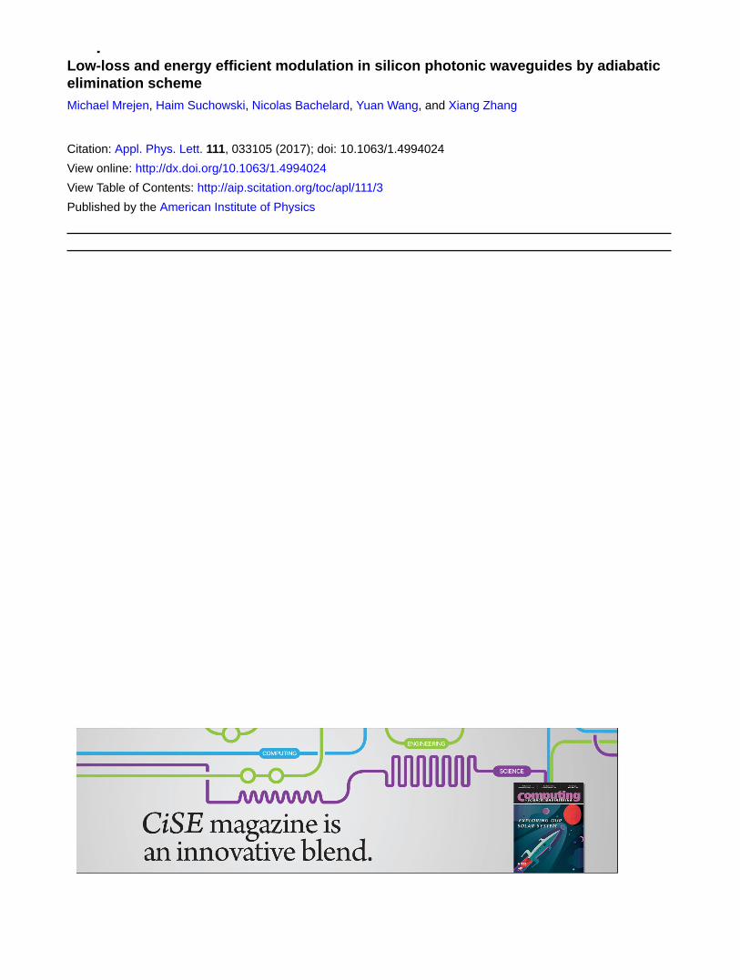
FIG. 1. Schematic of the Adiabatic Elimination modulation scheme where
three collinear waveguides are packed beyond the diffraction limit. This
results in strong couplings between all the waveguides (all are strongly cou-
pled). In this regime, in addition to strong couplings, there must be a strong
detuning between the waveguide modes such as jDb12j,jDb23j�V12,V23,
with Dbij being the phase mismatch between waveguides i and j and Vij
being the coupling between them. Once the AE regime is reached, the mid-
dle waveguide is effectively decoupled from the outer waveguides.
However, controlling the mode index of the decoupled middle waveguide
affects the propagation dynamics of a signal propagating back and forth
between the outer waveguides and thus modulates the output power out of
waveguides 1 and 3. The mode index control mechanism in the middle
waveguide can be electrical, optical, thermal, or mechanical.
a)Present address: Raymond and Beverly Sackler School of Physics and
Astronomy, Tel Aviv University, Tel Aviv 69978, Israel.b)Author to whom correspondence should be addressed: xiang@berkeley.
edu
0003-6951/2017/111(3)/033105/4/$30.00 Published by AIP Publishing.111, 033105-1
APPLIED PHYSICS LETTERS 111, 033105 (2017)
In contrast to conventional waveguide modulators, the losses
in the AE scheme are mainly induced by the control applied
only on the middle waveguide, which supports a dark mode.4
Therefore, the control-induced losses do not affect the signal,
which is carried by the two outer modes. Moreover, since the
modulation is achieved through the manipulation of the mid-
dle-waveguide-mode refractive index, the control mecha-
nism can independently be electrical, thermal, optical, or
mechanical. Without the loss of generality, here, the control
is achieved through the propagation of an optical pulse in the
middle waveguide.
The real part of the refractive index is modulated by the
Kerr effect originating from silicon’s third order nonlinear-
ity, v(3), and the loss is induced by Two Photon Absorption
(TPA) and Free Carrier Absorption (FCA). We model the
propagation of the control pulse by a modified Non-Linear
Schr€odinger Equation (NLSE)5,6
@A
@zþ al
2A ¼ ijjAj2A� af
2A; (2)
where A is the slowly varying amplitude, al the linear loss, jthe nonlinear coefficient, and af the TPA loss. In Eq. (2), the
effects of dispersion are neglected. Indeed, if the group veloc-
ity dispersion in silicon wires can be significantly enhanced
compared to bulk silicon, it does not mean that a sensible tem-
poral distortion is induced over a short distance.7 In our case,
we estimate that a 140 fs-long pulse propagating over 300 lm
is only broadened by 150 fs.4 The nonlinear coefficient in Eq.
(2) reads j ¼ n2k0
Aeffþ i C
2, where n2 ¼ 2� 10�18 m2
W is the Kerr
coefficient and C is derived from the TPA coefficient
bTPA ¼ Aeff C ¼ 5� 10�12m=W.5,6 The effective area of the
middle-waveguide mode, Aeff , is defined as6
Aeff ¼Ð ÐjEyj2dxdy
� �2
Ð ÐjEyj4dxdy
: (3)
In the following, we consider a silicon buried in the silica
substrate middle-waveguide of width 275 nm and height
340 nm, which sustains a TM mode whose effective area is
estimated from Eq. (3) to be Aeff ¼ 0:11lm2. FCA is
included by af ¼ rN, where r ¼ 1:45� 10�21m2 for sili-
con6 and N is the carrier density produced by TPA. The car-
rier density is related to the field amplitude by6
@N
@t¼ bTPA
2ht0
jAj4
A2eff
� N
sc; (4)
where sc is the effective carrier lifetime (sc ¼ 0:5 ns).6,8 For a
repetition rate (80 MHz) lower than 1=sc, the free carriers
mostly recombine between two pulses. This simplification
reduces the problem to a single-pulse propagation. Combining
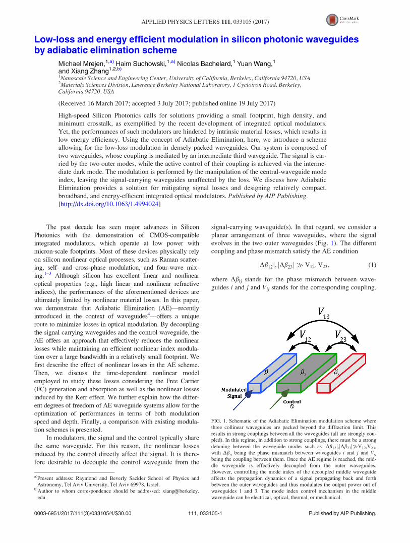
Eqs. (2) and (4), we plot in Fig. 2(a) the pulse propagation for
an input peak power of 400 W. The output pulse matches the
input-pulse shape, meaning that the long-lived FCA effect is
negligible. A weak FCA is further confirmed in Fig. 2(b),
showing the evolution of the FC density, N during the pulse
propagation. At any time and for any propagation length, Fig.
2(b) shows that the FC density induced by the pulse is several
orders of magnitude lower than the typical carrier
concentrations needed to affect tangibly the index of refraction
of silicon (1017–1018 cm�3 (Ref. 9) compared to 1011 cm�3
here). Therefore, under previously reported experimental con-
ditions, the fast Kerr nonlinearity dominates the slow FC
effect. It should be noted that the nonlinear Kerr effect is con-
sidered instantaneous because it relies on bound electrons, and
therefore, the all-optical modulation can be ultrafast (as already
been observed in Ref. 4). However, should a fast (>1 GHz)
electronic modulation be desired, considerations such as the
capacitance of the electrodes and travelling-wave configuration
have to be taken into account as in any modulator, which are
beyond the scope of the present work.
Having determined the mechanism at the origin of the
modulation, we can also evaluate the loss expected from an
optical control performed through the Kerr effect. The NLSE
[Eq. (2)] allows us to evaluate the attenuation induced by the
imaginary part of the refractive index j
lnIout
Iin
� �¼ � 4pj
klprop: (5)
We deduce from Eq. (5) that the loss induced by the control
pulse in the middle waveguide is ImðnÞ ¼ j ¼ 4:6� 10�5.
The AE condition is also satisfied when the middle wave-
guide is lossy either because of linear losses originating from
the imaginary part of the refractive index (e.g., plasmonic and
near resonant interactions) or because of nonlinear losses origi-
nating from the imaginary part of nonlinear susceptibility (e.g.,
TPA in Silicon Photonics). In that regard, the AE modulation
scheme offers a route to loss tolerant modulation. When losses
are present in the middle waveguide, the corresponding mode
FIG. 2. (a) Results from the modified NLSE showing no temporal distortion
due to FC after propagation of the 400 W peak power pump pulse in the mid-
dle waveguide (blue curve: pump beam at the input; red curve: pump beam
at the output). (b) Spatio-temporal dependence of the pump-induced free
carrier concentration along a 300 lm long Silicon waveguide. It is apparent
that the FC is significantly negligible compared to sensible concentrations
used to modulate the refractive index.
033105-2 Mrejen et al. Appl. Phys. Lett. 111, 033105 (2017)
index is modified to include an imaginary part, while the
signal-carrying mode indices remain real: b1 ¼ 2pk neff
1 ; b2
¼ 2pk neff
2 þ ijeff2 ; b3 ¼ 2p
k neff3 . Nevertheless, since the AE mini-
mizes the signal propagation in the middle waveguide, it leads
to a dramatic reduction in the effective signal loss coefficient
by several orders of magnitude.
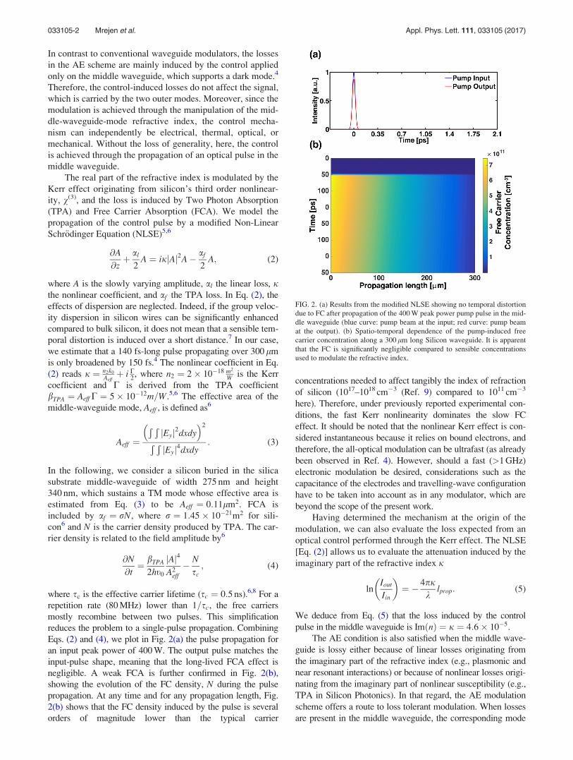
To show this behavior, we compare two cases. In the first
case, we consider a three waveguide AE configuration, where
the imaginary part of the middle-waveguide refractive index
is set to j2 ¼ 4:6� 10�5 as estimated in the previous para-
graph. The second case is a two-waveguide coupler where the
coupling yields an equivalent inversion length compared to
the first AE case. Although the losses considered here are
induced by the strong control pump through TPA and FCA,
the analysis presented here is valid for other loss mechanisms
such as metallic contacts or plasmonic waveguides. In a
numerical analysis carried out using an EigenMode
Expansion (EME) method10 on COMSOL, we have simulated
the propagation of a signal injected in waveguide #1 (outer
waveguide see Fig. 1). In the two-waveguide case, the loss is
considered in both waveguides since the intense pump oscil-
lates between the 2 waveguides and induces TPA and FCA in
both waveguides. For the three-waveguide AE case, the loss is
considered in the middle waveguide, as the intense pump
propagates only along the middle waveguide.
As shown in Figs. 3(a) and 3(b), the effective loss experi-
enced by the signal in the three-waveguide AE configuration is
significantly reduced compared to the standard two-waveguides
coupler (0.28 dB compared to 6.88 dB), despite the fact that the
same loss coefficient is considered in both cases. The origin of
the lower effective loss is related to the nature of the signal
propagation in the outer waveguides in the AE scheme. The
rate of light transfer to the middle waveguide is equal to the
rate of transfer from the middle waveguide, meaning that the
effective signal propagation there is significantly reduced. For
this reason, the AE of the lossy middle waveguide dramatically
reduces the overall loss of the modulator while still allowing
coupling control through the middle waveguide.
Several degrees of freedom available in the AE scheme,
namely, the direct couplings V12;V23, the indirect coupling
V13, and the phase mismatches Db12;Db23;Db13, allow for
the tuning of the effective coupling between the outer wave-
guides. This effective coupling can be exploited to improve
the extinction ratio and to reduce the power consumption. A
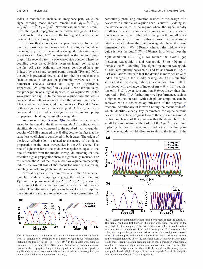
particularly promising direction resides in the design of a
device with a middle waveguide near its cutoff. By doing so,
the device operates in the regime where the signal rapidly
oscillates between the outer waveguides and then becomes
much more sensitive to the index change in the middle con-
trol waveguide. To exemplify this approach, we have simu-
lated a device where the outer waveguides have the same
dimensions (W1¼W3¼220 nm), whereas the middle wave-
guide is near the cutoff (W2¼170 nm). In order to meet the
right condition (V13 >V2
12
Db), we reduce the overall gap
(between waveguide 1 and waveguide 3) to 470 nm to
increase the V13 coupling. The signal injected in waveguide
#1 oscillates quickly between #1 and #3 as shown in Fig. 4.
Fast oscillations indicate that the device is more sensitive to
index changes in the middle waveguide. Our simulation
shows that in this configuration, an extinction ratio of 20 dB
is achieved with a change of index of Dn ¼ 9 � 10�4 requir-
ing only 8 pJ (power consumption 9 times lower than that
reported in Ref. 4). A further improved performance, such as
a higher extinction ratio with sub pJ consumption, can be
achieved with a dedicated optimization of the degrees of
freedom. Additionally, it is worth noting the recent review11
which identifies clearly key parameters for optoelectronic
devices to be able to progress toward the attoJoule regime. A
central conclusion of this review is that the device has to be
small for a modulator on the order of 0.03 lm3. In our case,
replacing the control waveguide (middle) with a thin plas-
monic waveguide would allow us to shrink the length of the
FIG. 3. Tolerance to the induced loss in an AE three-waveguide configura-
tion. (a) Simulation of propagation in a three-waveguide AE configuration
including the loss of ImðnÞ ¼ j ¼ 4:6� 10�5 in the middle waveguide as
evaluated from the generalized NLS model. We observe very minute signal
loss since the propagation length of the signal in the middle waveguide is
significantly reduced. As a comparison, an equivalent two-waveguide sys-
tem is calculated under the same conditions (b).
FIG. 4. Adiabatic elimination with the middle waveguide near the cutoff. (a)
The signal oscillates fast between the outer waveguides because of the
increased effective coupling. The fast oscillations make the configuration
more sensitive to modulation of the middle waveguide. To demonstrate this
point, we compare the modulation performances of the configuration tested
in Ref. 4 with the proposed configuration near the cutoff. (b) As we can see,
in the configuration used in Ref. 1, the signal oscillates slowly in waveguide
1, and thus, it requires a significant amount of index change in waveguide 2
to achieve a sensible output modulation in waveguide 1. (c) On the other
hand, in the configuration near the cutoff, the signal oscillates very fast in
waveguide 1 and a slight change of index in waveguide 2 results in a signifi-
cant modulation of output from waveguide 1.
033105-3 Mrejen et al. Appl. Phys. Lett. 111, 033105 (2017)
device bringing the active volume of the device to the order
of 0.05 lm3. As pointed above, we emphasize that the AE
configuration, by minimizing the amount of optical power
transiting in the control waveguide, makes this plasmonic
approach feasible with respect to metallic losses.
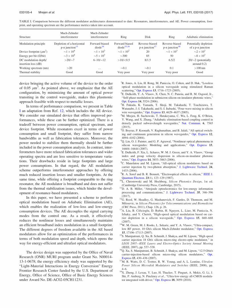
In terms of performance comparison, we present in Table
I an adaptation from Ref. 12, which includes the AE device.
We consider our simulated device that offers improved per-
formances, while these can be further optimized. There is a
tradeoff between power consumption, optical spectrum, and
device footprint. While resonators excel in terms of power
consumption and small footprint, they suffer from narrow
bandwidths as well as fabrication tolerances. Moreover, the
power needed to stabilize them thermally should be further
included in the power consumption analysis. In contrast, inter-
ferometers have more relaxed fabrication tolerances and wider
operating spectra and are less sensitive to temperature varia-
tions. Their drawbacks reside in large footprints and large
power consumptions. In that regard, the AE modulation
scheme outperforms interferometer approaches by offering
much reduced insertion losses and smaller footprints. At the
same time, while offering a footprint comparable to the ring
resonator, the AE modulator is broadband and does not suffer
from the thermal stabilization issues, which hinder the devel-
opment of resonance-based modulators.
In this paper, we have presented a scheme to perform
optical modulation based on Adiabatic Elimination (AE),
which enables the realization of low-loss and low-energy
consumption devices. The AE decouples the signal carrying
modes from the control one. As a result, it effectively
reduces the nonlinear losses and simultaneously maintains
an efficient broadband index modulation in a small footprint.
The different degrees of freedom available in the AE based
modulators allow for an optimization of the performances in
terms of both modulation speed and depth, which opens the
way for energy-efficient and ultrafast optical modulators.
The device design was supported by the Office of Naval
Research (ONR) MURI program under Grant No. N00014-
13-1-0678; the energy efficiency study was supported by the
“Light-Material Interactions in Energy Conversion” Energy
Frontier Research Center funded by the U.S. Department of
Energy, Office of Science, Office of Basic Energy Sciences
under Award No. DE-AC02-05CH11231.
1R. Jones, A. Liu, H. Rong, M. Paniccia, O. Cohen, and D. Hak, “Lossless
optical modulation in a silicon waveguide using stimulated Raman
scattering,” Opt. Express 13, 1716–1723 (2005).2E. Dulkeith, Y. A. Vlasov, X. Chen, N. C. Panoiu, and R. M. Osgood, Jr.,
“Self-phase-modulation in submicron silicon-on-insulator photonic wires,”
Opt. Express 14, 5524 (2006).3H. Fukuda, K. Yamada, T. Shoji, M. Takahashi, T. Tsuchizawa, T.
Watanabe, J.-I. Takahashi, and S.-I. Itabashi, “Four-wave mixing in silicon
wire waveguides,” Opt. Express 13, 4629–4637 (2005).4M. Mrejen, H. Suchowski, T. Hatakeyama, C. Wu, L. Feng, K. O’Brien,
Y. Wang, and X. Zhang, “Adiabatic elimination-based coupling control in
densely packed subwavelength waveguides,” Nat. Commun. 6, 7565
(2015).5€O. Boyraz, P. Koonath, V. Raghunathan, and B. Jalali, “All optical switch-
ing and continuum generation in silicon waveguides,” Opt. Express 12,
4094–4102 (2004).6Q. Lin, O. J. Painter, and G. P. Agrawal, “Nonlinear optical phenomena in
silicon waveguides: Modeling and applications,” Opt. Express 15,
16604–16644 (2007).7E. Dulkeith, F. Xia, L. Schares, W. M. J. Green, and Y. A. Vlasov, “Group
index and group velocity dispersion in silicon-on-insulator photonic
wires,” Opt. Express 14, 3853–3863 (2006).8C. Manolatou and M. Lipson, “All-optical silicon modulators based on
carrier injection by two-photon absorption,” J. Lightwave Technol. 24,
1433 (2006).9R. A. Soref and B. R. Bennett, “Electrooptical effects in silicon,” IEEE J.
Quantum Electron. 23(1), 123–129 (1987).10L. Chrostowski and M. Hochberg, Silicon Photonics Design, 1st ed.
(Cambridge University Press, Cambridge, 2015).11D. A. B. Miller, “Attojoule optoelectronics for low-energy information
processing and communications,” J. Lightwave Technol. 35, 346–396
(2017).12G. Reed, W. Headley, G. Mashanovich, F. Gardes, D. Thomson, and M.
Milosevic, in Silicon Photonics for Telecommunications and Biomedicine(CRC Press, 2011), Chap. 126, p. 26.
13A. Liu, B. Ciftcioglu, D. Rubin, H. Nguyen, L. Liao, M. Paniccia, N.
Izhaky, and Y. Chetrit, “High-speed optical modulation based on car-
rier depletion in a silicon waveguide,” Opt. Express 15, 660–668
(2007).14W. M. Green, M. J. Rooks, L. Sekaric, and Y. A. Vlasov, “Ultra-compact,
low RF power, 10 Gb/s silicon Mach-Zehnder modulator,” Opt. Express
15, 17106–17113 (2007).15S. Manipatruni, Q. Xu, B. Schmidt, J. Shakya, and M. Lipson, “High speed
carrier injection 18 Gb/s silicon micro-ring electro-optic modulator,” in
LEOS 2007—IEEE Lasers and Electro-Optics Society Annual Meeting(IEEE, 2007), pp. 537–538.
16Q. Xu, S. Manipatruni, B. Schmidt, J. Shakya, and M. Lipson, “12.5 Gbit/s
carrier-injection-based silicon micro-ring silicon modulators,” Opt.
Express 15, 430–436 (2007).17M. R. Watts, D. C. Trotter, R. W. Young, and A. L. Lentine, Ultralow
Power Silicon Microdisk Modulators and Switches (IEEE, 2008), pp.
4–6.18X. Zheng, J. Lexau, Y. Luo, H. Thacker, T. Pinguet, A. Mekis, G. Li, J.
Shi, P. Amberg, N. Pinckney et al., “Ultra-low-energy all-CMOS modula-
tor integrated with driver,” Opt. Express 18, 3059 (2010).
TABLE I. Comparison between the different modulator architectures demonstrated to date: Resonators, interferometers, and AE. Power consumption, foot-
print, and operating spectrum are the performance metrics taken into account.
Structure
Mach-Zehnder
interferometer
Mach-Zehnder
interferometer Ring Disk Ring Adiabatic elimination
Modulation principle Depletion of a horizontal
p-n junction13
Forward biased
diode14
Forward biased
diode15,16
Reverse-biased
p-n junction17
Reverse-biased
p-n junction18
Potentially depletion
of a p-n junction
Device footprint (lm2) �1� 104 �1� 103 �1� 102 20 �1� 103 �2� 102
Energy per bit (fJ/bit) �3� 104 �5� 103 �300 85 50 �8� 103
DC modulation depth/
insertion loss (dB)
>20/�7 6–10/�12 >10/<0.5 8/1.5 6.5/2 20/�2 (potentially
around 0.2)
Working spectrum (nm) >20 … �0.1 �0.1 0.1 >100 nm
Thermal stability Good Good Very poor Very poor Very poor Good
033105-4 Mrejen et al. Appl. Phys. Lett. 111, 033105 (2017)
Related Documents