Materials Science-Poland, Vol. 27, No. 3, 2009 Electrostriction and electromechanical coupling in elastic dielectrics at nanometric interfaces O.P. THAKUR, A. KUMAR SINGH * School of Applied Sciences, Netaji Subhas Institute of Technology, Sector-3, Dwarka, New Delhi-110078, India Electrostrictive coefficients, expressed in terms of dielectric parameters and elastic constants, are ob- tained for elastic dielectrics. In most of the recent experiments concerning determination of electrostric- tive parameters in elastic dielectrics, several researchers used incorrect equations without considering the contribution from the edge effect, the shear stresses and suitable boundary conditions. This led to wrong predictions of experimental results particularly for materials with high Poisson ratios. Errors in the esti- mation of induced strains, varying from an underestimation of 202% to an overestimation of 168%, have been pointed out in the case of polycarbonate (PC). However, the contribution from the boundary condi- tions is very difficult to predict correctly and hence it is still unresolved. The electromechanical properties of the nanometric interface are also discussed. Due to significant electrostrictive and piezoelectric charac- teristics of the nanometric interface, PC has a great potential for electromechanical applications as elec- tromechanical transducers, sensors and actuators. Key words: nanodielectric; electrostriction; elastomer 1. Introduction The objective of this work is to provide a clear understanding of the possible mechanism involving various dielectric and mechanical parameters for electric field induced strains in elastic dielectrics. The elastic deformation of a dielectric material under the forces exerted by electrostatic fields is called electrostriction. The mechani- cal deformation (stresses and strains) induced in a dielectric material (generally non piezoelectric) under the influence of an electric field occurs in two processes. The Maxwell stress effect occurs due to variation in the electric field distribution under strain, and the phenomena of electrostriction occur due to variation in the dielectric properties of the material under strain. The deformed material is no longer isotropic, _________ * Corresponding author, e-mail: [email protected]

Welcome message from author
This document is posted to help you gain knowledge. Please leave a comment to let me know what you think about it! Share it to your friends and learn new things together.
Transcript
Materials Science-Poland, Vol. 27, No. 3, 2009
Electrostriction and electromechanical coupling in elastic dielectrics at nanometric interfaces
O.P. THAKUR, A. KUMAR SINGH*
School of Applied Sciences, Netaji Subhas Institute of Technology, Sector-3, Dwarka, New Delhi-110078, India
Electrostrictive coefficients, expressed in terms of dielectric parameters and elastic constants, are ob-tained for elastic dielectrics. In most of the recent experiments concerning determination of electrostric-tive parameters in elastic dielectrics, several researchers used incorrect equations without considering the contribution from the edge effect, the shear stresses and suitable boundary conditions. This led to wrong predictions of experimental results particularly for materials with high Poisson ratios. Errors in the esti-mation of induced strains, varying from an underestimation of 202% to an overestimation of 168%, have been pointed out in the case of polycarbonate (PC). However, the contribution from the boundary condi-tions is very difficult to predict correctly and hence it is still unresolved. The electromechanical properties of the nanometric interface are also discussed. Due to significant electrostrictive and piezoelectric charac-teristics of the nanometric interface, PC has a great potential for electromechanical applications as elec-tromechanical transducers, sensors and actuators.
Key words: nanodielectric; electrostriction; elastomer
1. Introduction
The objective of this work is to provide a clear understanding of the possible mechanism involving various dielectric and mechanical parameters for electric field induced strains in elastic dielectrics. The elastic deformation of a dielectric material under the forces exerted by electrostatic fields is called electrostriction. The mechani-cal deformation (stresses and strains) induced in a dielectric material (generally non piezoelectric) under the influence of an electric field occurs in two processes. The Maxwell stress effect occurs due to variation in the electric field distribution under strain, and the phenomena of electrostriction occur due to variation in the dielectric properties of the material under strain. The deformed material is no longer isotropic,
_________
*Corresponding author, e-mail: [email protected]
O.P. THAKUR, A. KUMAR SINGH 840
and the scalar permittivity (ε) becomes a dielectric tensor (εij) due to anisotropic di-electric properties, in the case of an elastic dielectric material.
In equilibrium, the total forces, i.e. the total internal body forces Fint and the total external forces Fext such as forces due to a gravitational field, in every volume element of elastic dielectrics must be balanced to a zero value [1]:
3
int1
0 or 0ijext i
j j
TF F g
xρ
=
∂+ = + =
∂∑ (1)
where Fext = ρgi is an external force due to a gravitational field gi in a vertically downward direction Γ and Tij is the mechanical stress tensor. If there is another exter-nal force instead of a gravitational force, then the vector ρgi on the right hand side of above Eq. (1) must be replaced accordingly. But in the absence of external field, we have
3
10ij
j j
Tx=
∂=
∂∑ (2)
The strain tensor, Sij, describes the state of an elastic dielectric material subjected to a small deformation, and is given as
1 for2
jiij ji
j i
ssS S i jx x
⎛ ⎞∂∂= = + ≠⎜ ⎟⎜ ⎟∂ ∂⎝ ⎠
(3)
where s is a displacement vector. As the deformation is extremely small, only the first order terms in Sij have been
considered in the variation of components of the dielectric tensor εij and the dielectric tensor is given as
01 2ij ij ij kk ija S a Sε ε δ δ= + + (4)
where ε0 is the permittivity of the undeformed body, and a1 and a2 are two parameters
describing the variation in the dielectric properties of the material under shear and bulk deformations, respectively. The general form of the dielectric tensor, εij, for the deformed material is
0ij ij ijkl kla Sε ε= + (5)
where aijkl is a constant tensor of rank four. For linear and anisotropic dielectric under small deformation, the variation in the
dielectric tensor εij is given as
Electrostriction and electromechanical coupling in elastic dielectrics 841
3 3
1 1ij ijkl kl
k la Sδε δ
= =
=∑∑ (6)
and the coefficients
ijijkl
kl
aSε∂
=∂
(7)
represent a tensor of rank four characteristic of dielectrics, and also have different values at different points in an inhomogeneous dielectric medium. However, all but two classes of coefficients are approximately zero, namely the body strain coefficients aiiii and aiijj and the shear strain coefficients aijij [1].
Electromechanical phenomena have been observed in several macroscopic systems such as polycrystalline ceramics, ceramic polymer composites, several organic polymers, biopolymers, single crystals, systems with a liquid component, etc. However, this effect is very small in the case of solid dielectrics. Experimental data on the subject are not abun-dant, and the researchers [2, 3] frequently used an incorrect formula in the derivation of elastic strain with respect to the Maxwell stress effect, particularly in the case of polyure-thane elastomer (a cross-linked polymer), assuming various unrealistic approximations [4]. A linear electromechanical effect does not exist in the case of elastomers and Hooke’s law based on thermodynamic consideration (Helmoholtz free energy and Gibbs free energy concept) should not be applied for elastomers up to a large extent due to its nonlinear elas-tic behaviour. Electromechanical coupling effects in the case of non-piezoelectric material such as polyurethane elastomers have been exploited in the areas of fundamental sensors and actuators [5, 6]. Due to potential applications in sensing and actuation, the electrostric-tive response is very important [7].
The coupling between electrical and mechanical fields at the nanometric scale has been poorly exploited up to now. The interface between two dissimilar macroscopic phases in mutual contact has invariably different properties from the bulk on the either side in continuum. The electric fields at the interface induce a mechanical stress in addition to influencing polarization and conduction phenomena. The exploitation of the interface as electromechanical transducers is the real challenge in the development of nanometric dielectrics.
2. Electrostriction in elastic dielectrics: A theoretical approach
Fundamental assumptions of the theoretical approach to electrostriction in elastic dielectrics are as follows:
A. In unstrained state, electric and elastic properties are assumed to be isotropic. B. On application of an electric field, variations in permittivity are dependent on
the components of strain and as a result, the material becomes electrically anisotropic . C. In static equilibrium, the elastic forces induced during deformations will bal-
ance the mechanical forces induced by the static field.
O.P. THAKUR, A. KUMAR SINGH 842
D. The relation between the mechanical stress (Tij) and the strain (Sij) is governed by Hook’s law.
E. Deformation is extremely small. F. The dependence of D on E is linear even in an anisotropic dielectric and D and
E are parallel only along preferred axes, i.e.
3
01
i ij jj
D Eε ε=
= ∑
where ε0 is the permittivity of a free space. The Maxwell stress tensor [8] results from a force produced by the electric field
and is given as
( ) ( )0 0 0 20 01 22
2 2ij ij i j ijT T a E E a Eε εε ε δ= + − − + (8)
where 0ijT is the stress tensor in the absence of an electric field. Generally we tend to
neglect 0ijT in isotropic dielectrics but in the case of a dielectric interface, the presence
of a significant number of point defects introduces distortion in the interfacial region. In the case of a size difference of two particles from two phases, elastic stress and strains are created. A larger atom introduces compressive stress and the corresponding strain around it, while a smaller interacting atom creates a tensile stress–strain field. An interstitial atom also produces strain around the void it occupies.
If the direction of the electric field is assumed to be along the X3 axis (k direction) in the Cartesian coordinate system, the principal stresses induced electrically are
0 0 2 1 233 33 0 0
1 12
a aT T Eε εε+⎛ ⎞= − −⎜ ⎟
⎝ ⎠ (9)
0 0 2 211 22 11 0 0
1 12
aT T T Eε εε
⎛ ⎞= = + +⎜ ⎟⎝ ⎠
(10)
Where a1 = ∂ε/∂S1 = ∂ε/∂S2, due to strain in the X1X2 plane, and a2 = ∂ε/∂S3, expresses the increment in the field direction, i.e. along the X3 axis. 0
11T and 033T are the stresses
even in the absence of an external field, however these stresses are independent of the direction in the case of isotropic dielectrics, and it should not be neglected at the inter-face having a significant number of point defects. However, it is very difficult to evaluate 0
ijT precisely. For a linear elastic dielectric material (described by Hooke’s law), the electrically
induced stresses will also generate elastic stress and strain in equilibrium condition and the elastic stress tensor Tij [9] is given in terms of the elastic strain tensor, Sij, Young modulus Y and Poisson’s ratio, σ, by
Electrostriction and electromechanical coupling in elastic dielectrics 843
1 1 2ij ij kk ij
YT S Sσ δσ σ⎛ ⎞= +⎜ ⎟+ −⎝ ⎠
(11)
conversely
( )1 1ij ij kk ijS T TY
σ σ δ⎡ ⎤= + −⎣ ⎦ (12)
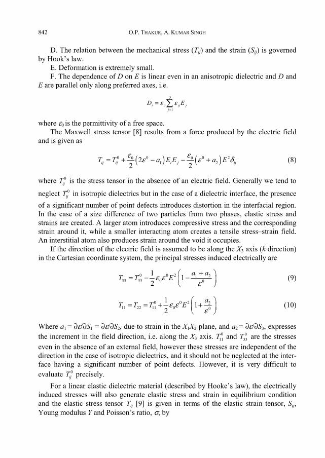
If the force acts only along the X3 direction, i.e. along the direction of the electric field E, then we have S11 = S22 = 0, and if the sides of dielectric material are also fixed (Fig. 1), we have S32 = S31 = 0.
Fig. 1. Schematic diagrams illustrating the effect of electric field E (acting along the X3 direction) on the elastic dielectric material enclosed between two parallel rigid electrodes: a) sides of a dielectric
slab are rigidly fixed as a result of this; no expansion in a lateral direction takes place, i.e., S31 = S32 = 0, b) sides of slab are open and a longitudinal compressive strain S33 acts along the X3 direction,
whereas the shear strains, S31 = S32, act along the X1 and X2 directions
For such a unilateral deformation, the principal elastic stresses and strains are
11 22 33(1 )(1 2 )YT T S
σ σ= =
+ − (13)
( )( )( )33 33
11 1 2
YT S
σσ σ
−=
+ − (14)
( )( )33
1 1 2(1 )
pS
Yσ σ
σ+ −
=−
(15)
where T33 = p is a compressive force, i.e. pressure. On substituting the principal value of the Maxwell stress tensor (assuming 0 0
11 33 0T T= = ) from Eqs. (9) and (10) into Eq. (12), we can express the principal elastic strains as
O.P. THAKUR, A. KUMAR SINGH 844
( ) 20 2 11
11 22 0 0 0
1 21 12
aaS S E Yσσε ε
ε ε−⎛ − ⎞
= = − +⎜ ⎟⎝ ⎠
(16)
( ) ( )1 20 2 133 0 0
1 21 1 22
a aS E Y
σε ε σ
ε−⎛ + − ⎞
= − + −⎜ ⎟⎝ ⎠
(17)
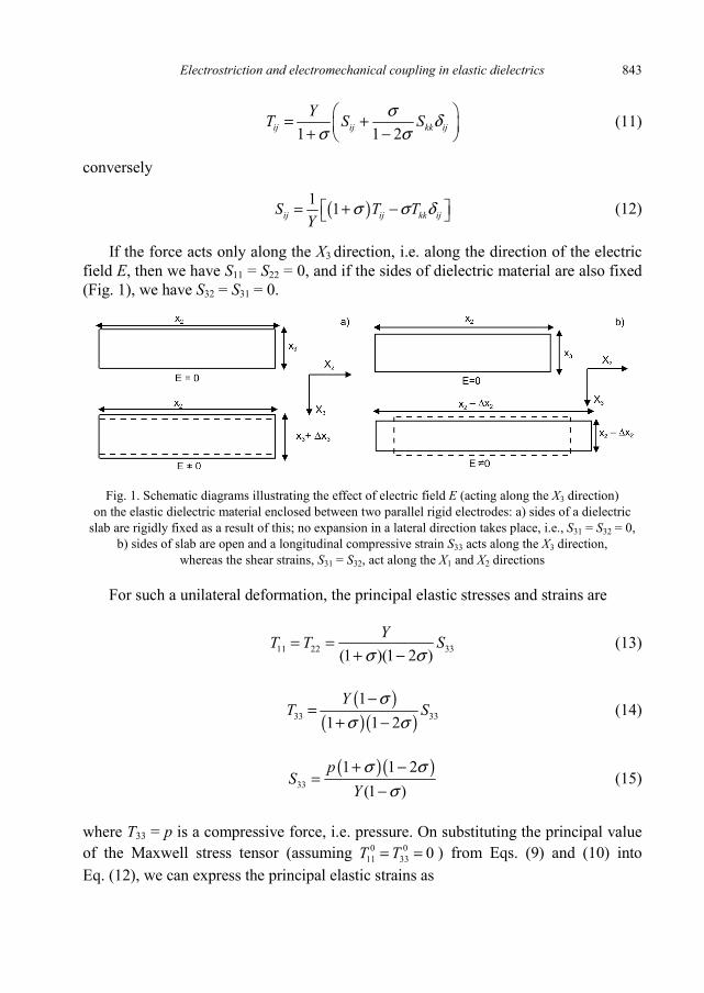
Fig. 2. Schematic diagram illustrating an elastic dielectric subjected to one normal electrical stress
along the X3 direction, causing compressive longitudinal strain S32 and two tensile shear strains,
S31 and S32 along the X1 and X2 directions, respectively, as the electric field has only one component along the X3 direction. If E also has other components, then there are other principal strains S11 = S22 ≠ 0
The principal elastic strain, S33, represents the relative change in thickness of the interface, whereas the strain, S11 or S22, represents the relative change in the diameter of the capacitor, as described in [4], which is not correct in the case of a parallel plate capacitor in which S31 or S32 actually represent the lateral change in dimension, as E has only a component along X3 (Fig. 2), i.e. only one normal component of stress, T33, along with its two shearing components, T31 or T32. On comparing Eqs. (16) and (17) with a general equation for electrostriction ij ijkl k lS E Eγ= (18)
we get
2 211 22 31 33 33,S S E S Eγ γ= = = − (19)
where γ31 and γ33 are the electrostrictive coefficients. A negative sign for the strain S33 indicates that it is a contraction along X3 and S11 and S22 are tractions, so causing ex-pansion along the X1 and X2 directions.
3. Interface as an electromechanical transducer
Macroscopic electromechanical behaviour arises from interactions occurring at the nanometric interface. At the nanodielectric interface between two phases, the segrega-tion of charge clusters and double layer polarization are responsible for producing
Electrostriction and electromechanical coupling in elastic dielectrics 845
electrostriction in the presence of a non-uniform electric field. If the electric field E is changed to E + ΔE, the change in S33 becomes
33 33 0 33Δ 2 Δ ΔS E E Eλ μ= − = (20)
where μ33 is the piezoelectric coefficient. Similarly, the coefficient μ31 and μ32 can be found along the X1 and X2 directions. The piezoelectric transverse coefficients have been frequently used [10] in piezoelectric thin film devices. The average value of compressive elastic strain induced along the X3 direction is
33 30
ΔK S dxλ
∫ (21)
where λ is the Debye–Hückel length. Similarly, the expression for the tensile strains (ΔS32 and ΔS31) along the X1 and X2 directions can be obtained.
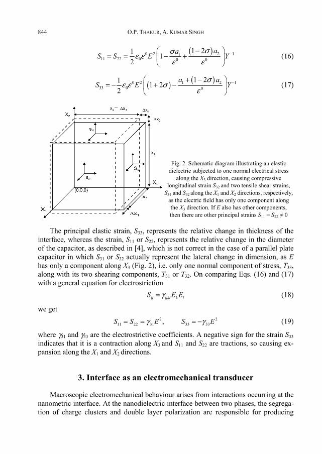
Fig. 3. Schematic diagram showing the formation of electric double layer formed due to segregation of
charge clusters at an electrode–electrolyte interface. The distribution of a nonuniform electric field in
noncentrosymmetric interface is also shown
At the electrode–electrolyte interface (Fig. 3) having decaying electric fields from the electrode surface, the only modification required for the calculation of E2 is
2 23 3
0
1 ( )E E x dxλ
λ= ∫ (22)
The integration is over the thickness of the double layer, i.e. the Debye–Hückel length λ. If E has only one component along the X3 direction, we should consider the longi-
tudinal component S33 and the transverse components S32 and S31, and neglect the prin-
O.P. THAKUR, A. KUMAR SINGH 846
cipal strains, S11 and S22, as E has no components along the X1 and X2 direction but the actual boundary conditions satisfied (after deformations) at the interface between an electrode and dielectric are the points of main concern, and it is very difficult to cor-rectly predict the contributions from boundary conditions. If E has small components along the X1 and X2 directions, we should not neglect the principal elastic strains S11
and S22.
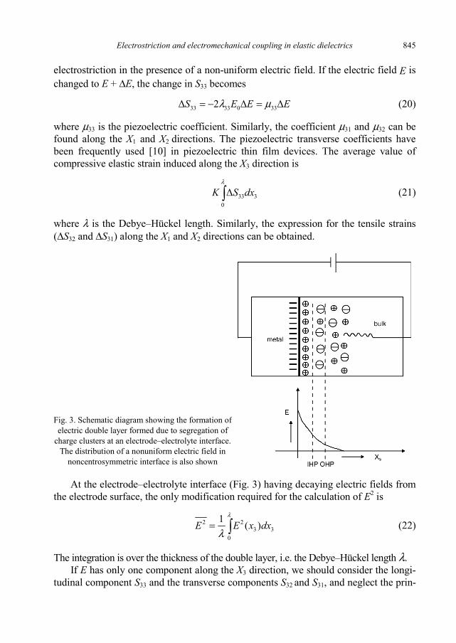
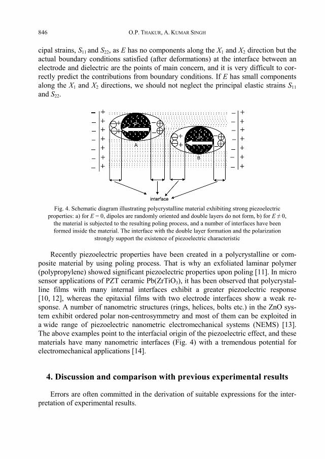
Fig. 4. Schematic diagram illustrating polycrystalline material exhibiting strong piezoelectric properties: a) for E = 0, dipoles are randomly oriented and double layers do not form, b) for E ≠ 0,
the material is subjected to the resulting poling process, and a number of interfaces have been formed inside the material. The interface with the double layer formation and the polarization
strongly support the existence of piezoelectric characteristic
Recently piezoelectric properties have been created in a polycrystalline or com-posite material by using poling process. That is why an exfoliated laminar polymer (polypropylene) showed significant piezoelectric properties upon poling [11]. In micro sensor applications of PZT ceramic Pb(ZrTiO3), it has been observed that polycrystal-line films with many internal interfaces exhibit a greater piezoelectric response [10, 12], whereas the epitaxial films with two electrode interfaces show a weak re-sponse. A number of nanometric structures (rings, helices, bolts etc.) in the ZnO sys-tem exhibit ordered polar non-centrosymmetry and most of them can be exploited in a wide range of piezoelectric nanometric electromechanical systems (NEMS) [13]. The above examples point to the interfacial origin of the piezoelectric effect, and these materials have many nanometric interfaces (Fig. 4) with a tremendous potential for electromechanical applications [14].
4. Discussion and comparison with previous experimental results
Errors are often committed in the derivation of suitable expressions for the inter-pretation of experimental results.
Electrostriction and electromechanical coupling in elastic dielectrics 847
4.1. Contributions from shear stresses
The electromechanical response of the polyurethane elastomer (Dow 2103-80AE) has been obtained and the relative change in the thickness of a dielectric slab between the electrodes of a capacitor has been experimentally determined [3] without consider-ing lateral stresses, the edge effect, boundary conditions and the tensor form of permit-tivity. The equation used may be written as:
0 230 33
3
12
x E Sx Y
Δ ε ε= = (23)
However the correct mathematical expression can be seen from Eq. (17), which indi-cates that neglecting the lateral stress and the Poisson ratio leads to underestimation of Δx3/x3. Similarly, another researcher [2] used Maxwell’s principal stress (Eq. (9)) for the determination of relative change in the thickness of a dielectric slab, neglecting the contri-butions from lateral elastic stresses and the edge effect. Here, the expression used was
0 23 1 20 0
3
1 12
x a aEx Y
Δ ε εε+⎛ ⎞= − −⎜ ⎟
⎝ ⎠ (24)
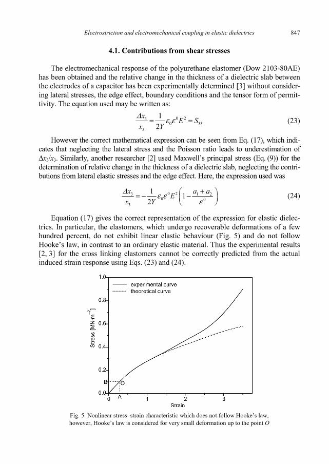
Equation (17) gives the correct representation of the expression for elastic dielec-trics. In particular, the elastomers, which undergo recoverable deformations of a few hundred percent, do not exhibit linear elastic behaviour (Fig. 5) and do not follow Hooke’s law, in contrast to an ordinary elastic material. Thus the experimental results [2, 3] for the cross linking elastomers cannot be correctly predicted from the actual induced strain response using Eqs. (23) and (24).
Fig. 5. Nonlinear stress–strain characteristic which does not follow Hooke’s law, however, Hooke’s law is considered for very small deformation up to the point O
O.P. THAKUR, A. KUMAR SINGH 848
Theoretically, Poisson’s ratio (σ) varies from –1 to 0.5 but in practice no material is available with σ < 0 [9]. Poisson’s ratio for polymers has been found to be ca. 0.5 [15]. Neglect of lateral stresses, particularly in the case of elastic dielectrics or poly-mers with high Poisson’s ratio, and using Eq. (9) leads to incorrect estimation of the electrically induced strain. On putting σ = 0.5 in Eq. (17), we get
0 2 1133 0
0
1 22
aS E Yε εε
−⎡ ⎤= − −⎢ ⎥
⎣ ⎦ (25)
and this is quite different from Eq. (9), in the sense that the contribution from the term a2 has been cancelled due to the presence of the (l – 2σ) term in Eq. (17). Actually the longitudinal principal strain S33 calculated from Eq. (25) is twice the value of the strain calculated in [3] from Eq. (23) for a material with σ = 0.5 and a1 = 0. Errors in the estimations of induced strains can be pointed out in the case of polycarbonate (PC). The following data for polycarbonate are given [16]: |a1| = 1.404, |a2| = 2.6, 2 2.6a = , ε0 = 2.9* at 1 MHz, σ = 0.37 at 1 MHz.
Comparing Eqs. (23) and (24) with Eq. (17), after substituting the above data, an overestimation of 168% and an underestimation of 202%, respectively, have been found.
The use of the correct Eq. (17) is necessary, particularly for the material having a high Poisson’s ratio. Using the dielectric constant and the elastic compliance data, the contribution of the Maxwell stress to the total strain response can be determined.
If the sides of the dielectric slab/interface are rigidly fixed, the effective stiffness (T33/S33) is governed by Eq. (14). The dielectric parameters, a1 and a2, are experimen-tally obtained [16] by determining dε33/dS33 in constrained and unconstrained condi-tions, and using Eq. (4). However, the linearity of the theory of electrostriction fails if the deformations are not quadratic in the applied field, particularly at a higher field strength.
In the case of dielectrics with a non-uniform field, e.g. cylindrical capacitor and nanometric interface, we should use either Eq. (22) or deal with the problem sepa-rately to evaluate 2E for the situation. In the presence of a non-uniform electric field with a high field strength, the phenomenon of dielectrophoresis takes place. However, it is in general a weak effect, particularly in the case of a solid dielectric.
4.2. Contributions from edge effects
Due to free edges of plates of a capacitor, the distribution of charge over them is not uniform. Hence a correction due to edge effects [8] is very much required for all practical purposes in which the thickness of the dielectric slab is comparable to its _________
*www.matweb.com.
Electrostriction and electromechanical coupling in elastic dielectrics 849
lateral dimension i.e., Δx3 ≈ (cross sectional area of plate)1/2. However, this correction may be neglected in the case of a thin film capacitor and a nanometric interface having a lateral dimension that is much greater relative to its thickness (typically of order a few nm).
4.3. Contribution from boundary conditions
For experimental study [3, 16], a parallel plate capacitor with a dielectric film/slab has been considered, due to its simple, symmetrical geometry. However, due to elec-trostrictive deformation, the permittivity of different regions (Fig. 1 shows two re-gions, one with an air gap and other with a dielectric medium) is different, thus the solution to the field or potential must be different although having the same general form of solution (to the Laplace equation). Appropriate electrical boundary conditions must be satisfied at the interface between the two regions.
For the mechanical boundary conditions, Eq. (1) must be satisfied in equilibrium, i.e. the external forces on the boundary may be regarded as a continuation of the inter-nal stress distribution.
However, it is very difficult to predict exact boundary conditions at the interface between electrodes and the dielectric or between two regions with different permittivi-ties. If the field is applied exactly along the X3 direction, the strain components, S33 (normal/bulk strain along X3), and S31 and S32 (shear strains along the X1 and X2 direc-tions) play the major role in the electromechanical phenomena exhibited by the inter-face in nanometric dielectrics [17].
5. Conclusion
In elastic dielectrics, shear and lateral stresses play a major role in the correct es-timation of induced elastic strain. Thus neglecting the contribution from lateral and shear stresses leads to overestimation or underestimation of the results. However, the boundary conditions at the interface between electrode and the dielectrics are the points of main concern, as it is very difficult to predict exact mechanical and electrical boundary conditions in deformed dielectrics. It has also been pointed out that nanometric dielectric interfaces, which are non-centrosymmetric systems, have tre-mendous potential for electromechanical applications. A lot of work has to be done, particularly in the field of biology, cellular polymers, biopolymers, intercellular biomembranes, etc. at the nanoscale level, in order to exploit nanometric interfaces for various applications as sensors, actuators and transducers.
References
[1] STRATTON J.A., Electromagnetic Theory, McGraw-Hill, New York, 1941. [2] SHKEL Y.M., KLINGENBERG D.J., J. Appl. Phys., 80 (1996), 4567.
O.P. THAKUR, A. KUMAR SINGH 850
[3] ZHANG Q.M., SU J., KIM C.H., TING R., CAPPS R., J. Appl. Phys., 81 (1997), 2770. [4] KRAKOVSKÝ L., ROMIJN T., POSTHUMA DE BOER A., J. Appl. Phys., 85 (1999), 628. [5] LADABAUM I., KHURI-YAKUB B.T., SPOLIANSKY D., Appl. Phys. Lett., 68 (1996), 7. [6] HERBERT J.M., Ferroelectric Transducers and Sensors, Gordon and Breach, New York, 1982. [7] Electroactive Polymer (EAP) Actuators as Artificial Muscles: Reality, Potential and Challenges, 2nd
Ed., Y. Bar-Cohen (Ed.), SPIE Press, Bellingham, WA, Vol. PM 136, 2004. [8] LANDAU L.D., LIFSHITZ L.M., Electrodynamics of Continuous Media, 2nd Ed., Pergamon Press, Ox-
ford, 1984. [9] LANDAU L.D., LIFSHITZ L.M., Theory of Elasticity, Pergamon Press, Oxford, 1970.
[10] KANNO I., KOTERA H., WASA K., Sensors Act. A, 107 (2003), 68. [11] MONTANARI G.C., IEEE Trans. DEI, 10 (2003), 615. [12] KANNO I., FUJII S., KAMADA T., TAKAYAMA R., Appl. Phys. Lett., 70 (1997), 1378. [13] WANG Z.L., Materials Today (2004), 26. [14] LEWIS T.J., J. Phys. D: Appl. Phys., 38 (2005), 202. [15] FERRY J.D., Viscoelastic Properties of Polymers, Wiley, New York, 1980. [16] LEE H.Y., PENG Y., SHKEL Y.M., J. Appl. Phys., 98 (2005), 074104. [17] THAKUR O.P., SINGH A.K., Electromechanical Phenomena at the Interface in Nanometric Dielec-
trics, Proc. 2nd Int. Conf. on Sensing Technology, ICST, Palmerston North, New Zealand, pp. 188–192, 2007.
Received 16 May 2008 Revised 28 November 2008
Related Documents