HAL Id: tel-03650450 https://tel.archives-ouvertes.fr/tel-03650450 Submitted on 25 Apr 2022 HAL is a multi-disciplinary open access archive for the deposit and dissemination of sci- entific research documents, whether they are pub- lished or not. The documents may come from teaching and research institutions in France or abroad, or from public or private research centers. L’archive ouverte pluridisciplinaire HAL, est destinée au dépôt et à la diffusion de documents scientifiques de niveau recherche, publiés ou non, émanant des établissements d’enseignement et de recherche français ou étrangers, des laboratoires publics ou privés. Electrostatics of charges in thin dielectric and ferroelectric films Svitlana Kondovych To cite this version: Svitlana Kondovych. Electrostatics of charges in thin dielectric and ferroelectric films. Other [cond- mat.other]. Université de Picardie Jules Verne, 2017. English. NNT: 2017AMIE0031. tel-03650450

Welcome message from author
This document is posted to help you gain knowledge. Please leave a comment to let me know what you think about it! Share it to your friends and learn new things together.
Transcript
HAL Id: tel-03650450https://tel.archives-ouvertes.fr/tel-03650450
Submitted on 25 Apr 2022
HAL is a multi-disciplinary open accessarchive for the deposit and dissemination of sci-entific research documents, whether they are pub-lished or not. The documents may come fromteaching and research institutions in France orabroad, or from public or private research centers.
L’archive ouverte pluridisciplinaire HAL, estdestinée au dépôt et à la diffusion de documentsscientifiques de niveau recherche, publiés ou non,émanant des établissements d’enseignement et derecherche français ou étrangers, des laboratoirespublics ou privés.
Electrostatics of charges in thin dielectric andferroelectric films
Svitlana Kondovych
To cite this version:Svitlana Kondovych. Electrostatics of charges in thin dielectric and ferroelectric films. Other [cond-mat.other]. Université de Picardie Jules Verne, 2017. English. NNT : 2017AMIE0031. tel-03650450
UNIVERSITY OF PICARDIE JULES VERNE
Electrostatics of charges in
dielectric and ferroelectric films
by
Svitlana KONDOVYCH
A thesis submitted in partial fulfillment for the
degree of Doctor of Philosophy
Laboratory of Condensed Matter Physics (EA 2081)
33, rue Saint-Leu - 80039 Amiens Cedex 1
2017
Electrostatics of charges
in dielectric and ferroelectric films
– ABSTRACT –
We explore the various types of electrostatic interaction between charges in
thin films with high dielectric permittivity, including the special case of the
two-dimensional logarithmic Coulomb interaction, and propose a method of
tuning the interaction regime using the external gate electrode. Changing the
gate-to-film distance, one may alter the electrostatic screening length of the
dielectric sample and control the ranges of different interaction types.
We investigate next the electrostatics of extended charges in dielectric media,
modeling the electrostatic potential distribution for charged wires, stripes and
domain walls, with either homogeneous or periodic linear charge density. Bas-
ing on the calculated dependencies of the potential on the system geometry
and material parameters, we discuss several possible applications: i) we suggest
the non-destructive method for measuring the dielectric constant of substrate-
deposited thin films by a two-wire capacitor; ii) we study the domain structure
formation in ferroelectric films with in-plane polarization.
We show that for the in-plane striped 180 domain structure, induced by the
discontinuity of the order parameter at the film edge, the equilibrium domain
width violates the Kittel’s square root law, being instead inversely proportional
to the film thickness. The calculations for the in-plane domains, generated by
the microscope tip or charged domain wall in the ferroelectric slab, demonstrate
the conformity of the optimal domain length to the characteristic electrostatic
length of the sample, and accord with the experimental data.
Keywords: electrostatic interactions, charge, dielectric, ferroelectric, domain.
This work was supported by EC-FP7 ITN-NOTEDEV project
Electrostatique des charges dans les couches
minces dielectriques et ferroelectriques
– RESUME –
Nous explorons la variete des types d’interactions electrostatiques entre les
charges dans des films minces a haute permittivite dielectrique, y compris
l’interaction de Coulomb bidimensionnel logarithmique. Nous proposons une
methode de reglage du regime d’interaction dans le couche a l’aide de l’electrode
externe. Nous etudions ensuite les electrostatiques des charges etendues dans
les materiaux dielectriques: des fils et des bandes charges de maniere homogene
ou periodique. En s’appuyant sur les potentiels electrostatiques calcules de ces
objets, nous abordons plusieurs applications possibles. Tout d’abord, nous
suggerons la methode non destructive pour mesurer la constante dielectrique
des films minces deposes par un substrat par un condensateur a deux fils.
Ensuite, nous etudions la formation des domaines dans des films ferroelectriques
avec la polarisation dans le plan. L’apparition de la texture en domaines est
causee soit par le bord charge d’un echantillon de taille finie, soit par l’existence
d’une paroi de domaine charge dans le film. Les deux phenomenes augmentent
l’energie electrostatique de l’echantillon, ce qui stimule l’apparence des do-
maines pour minimiser l’energie totale. Nous montrons que la taille equilibre
du domaine depend de la geometrie de l’echantillon et, pour les domaines dans
le plan, elle viole la loi racine carree de Kittel, etant inversement proportion-
nelle a l’epaisseur du film.
Mots-Cles: interaction electrostatique, charge, dielectrique, ferroelectrique,
domaine.
Les travaux de recherche etaient finances par le Projet Europeen FP7-MC-
ITN-NOTEDEV.
iv
Resume v
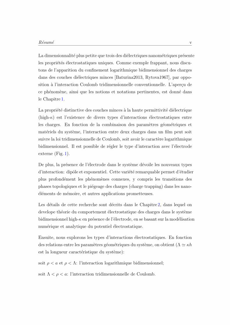
La dimensionnalite plus petite que trois des dielectriques nanometriques presente
les proprietes electrostatiques uniques. Comme exemple frappant, nous discu-
tons de l’apparition du confinement logarithmique bidimensionnel des charges
dans des couches dielectriques minces [Baturina2013, Rytova1967], par oppo-
sition a l’interaction Coulomb tridimensionnelle conventionnelle. L’apercu de
ce phenomene, ainsi que les notions et notations pertinentes, est donne dans
le Chapitre 1.
La propriete distinctive des couches minces a la haute permittivite dielectrique
(high-κ) est l’existence de divers types d’interactions electrostatiques entre
les charges. En fonction de la combinaison des parametres geometriques et
materiels du systeme, l’interaction entre deux charges dans un film peut soit
suivre la loi tridimensionnelle de Coulomb, soit avoir le caractere logarithmique
bidimensionnel. Il est possible de regler le type d’interaction avec l’electrode
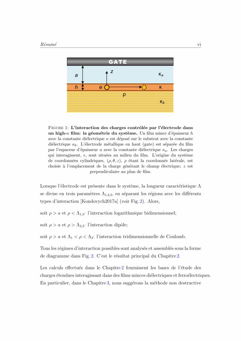
externe (Fig. 1).
De plus, la presence de l’electrode dans le systeme devoile les nouveaux types
d’interaction: dipole et exponentiel. Cette variete remarquable permet d’etudier
plus profondement les phenomenes connexes, y compris les transitions des
phases topologiques et le piegeage des charges (charge trapping) dans les nano-
elements de memoire, et autres applications prometteuses.
Les details de cette recherche sont decrits dans le Chapitre 2, dans lequel on
develope theorie du comportement electrostatique des charges dans le systeme
bidimensionnel high-κ en presence de l’electrode, en se basant sur la modelisation
numerique et analytique du potentiel electrostatique.
Ensuite, nous explorons les types d’interactions electrostatiques. En fonction
des relations entre les parametres geometriques du systeme, on obtient (Λ ' κh
est la longueur caracteristique du systeme):
soit ρ < a et ρ < Λ: l’interaction logarithmique bidimensionnel;
soit Λ < ρ < a: l’interaction tridimensionnelle de Coulomb.
Resume vi
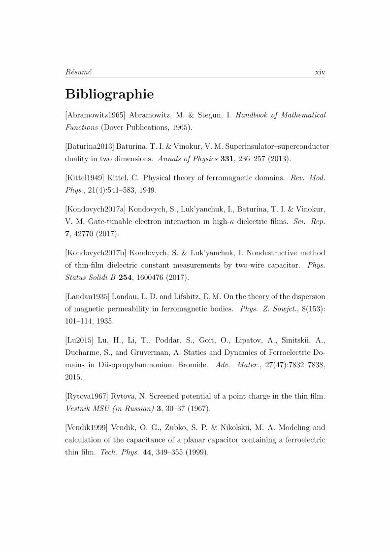
h
κa
κ
κb
ρ
a
GATE
e
z
Figure 1: L’interaction des charges controlee par l’electrode dansun high-κ film: la geometrie du systeme. Un film mince d’epaisseur havec la constante dielectrique κ est depose sur le substrat avec la constantedielectrique κb. L’electrode metallique en haut (gate) est separee du filmpar l’espaceur d’epaisseur a avec la constante dielectrique κa. Les chargesqui interagissent, e, sont situees au milieu du film. L’origine du systemede coordonnees cylindriques, (ρ, θ, z), ρ etant la coordonnee laterale, estchoisie a l’emplacement de la charge generant le champ electrique; z est
perpendiculaire au plan de film.
Lorsque l’electrode est presente dans le systeme, la longueur caracteristique Λ
se divise en trois parametres Λ1,2,3, en separant les regions avec les differents
types d’interaction [Kondovych2017a] (voir Fig. 2). Alors,
soit ρ > a et ρ < Λ1,3: l’interaction logarithmique bidimensionnel;
soit ρ > a et ρ > Λ2,3: l’interaction dipole;
soit ρ > a et Λ1 < ρ < Λ2: l’interaction tridimensionnelle de Coulomb.
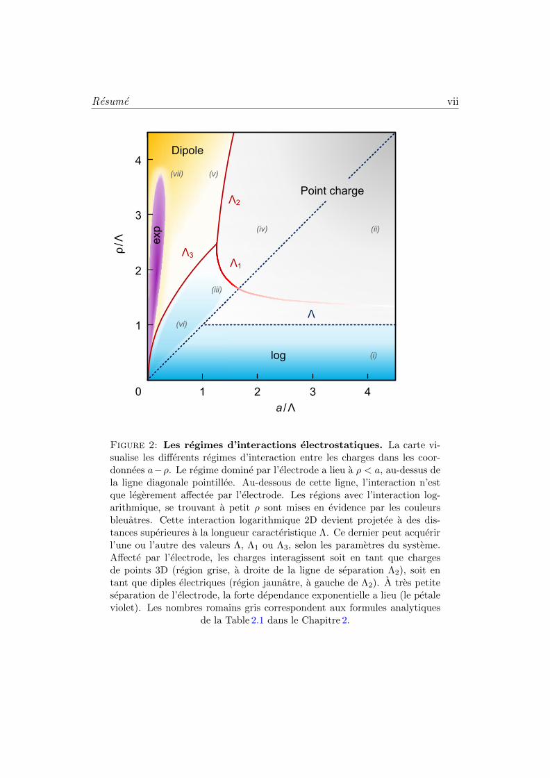
Tous les regimes d’interaction possibles sont analyses et assembles sous la forme
de diagramme dans Fig. 2. C’est le resultat principal du Chapitre 2.
Les calculs effectues dans le Chapitre 2 fournissent les bases de l’etude des
charges etendues interagissant dans des films minces dielectriques et ferroelectriques.
En particulier, dans le Chapitre 3, nous suggerons la methode non destructive
Resume vii
1 2 3 4
a /Λ
log
Dipole
Point charge
exp
Λ2
Λ3
1
2
3
4
ρ/Λ
0
Λ
(i)
(ii)(iv)
(v)(vii)
(vi)
(iii)
Λ1
Figure 2: Les regimes d’interactions electrostatiques. La carte vi-sualise les differents regimes d’interaction entre les charges dans les coor-donnees a−ρ. Le regime domine par l’electrode a lieu a ρ < a, au-dessus dela ligne diagonale pointillee. Au-dessous de cette ligne, l’interaction n’estque legerement affectee par l’electrode. Les regions avec l’interaction log-arithmique, se trouvant a petit ρ sont mises en evidence par les couleursbleuatres. Cette interaction logarithmique 2D devient projetee a des dis-tances superieures a la longueur caracteristique Λ. Ce dernier peut acquerirl’une ou l’autre des valeurs Λ, Λ1 ou Λ3, selon les parametres du systeme.Affecte par l’electrode, les charges interagissent soit en tant que chargesde points 3D (region grise, a droite de la ligne de separation Λ2), soit entant que diples electriques (region jaunatre, a gauche de Λ2). A tres petiteseparation de l’electrode, la forte dependance exponentielle a lieu (le petaleviolet). Les nombres romains gris correspondent aux formules analytiques
de la Table 2.1 dans le Chapitre 2.
Resume viii
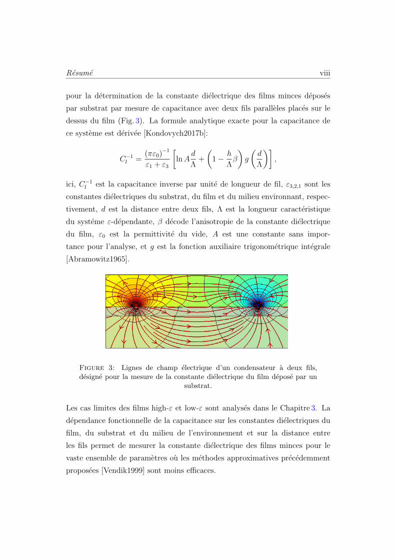
pour la determination de la constante dielectrique des films minces deposes
par substrat par mesure de capacitance avec deux fils paralleles places sur le
dessus du film (Fig. 3). La formule analytique exacte pour la capacitance de
ce systeme est derivee [Kondovych2017b]:
C−1l =
(πε0)−1
ε1 + ε3
[lnA
d
Λ+
(1− h
Λβ
)g
(d
Λ
)],
ici, C−1l est la capacitance inverse par unite de longueur de fil, ε3,2,1 sont les
constantes dielectriques du substrat, du film et du milieu environnant, respec-
tivement, d est la distance entre deux fils, Λ est la longueur caracteristique
du systeme ε-dependante, β decode l’anisotropie de la constante dielectrique
du film, ε0 est la permittivite du vide, A est une constante sans impor-
tance pour l’analyse, et g est la fonction auxiliaire trigonometrique integrale
[Abramowitz1965].
Figure 3: Lignes de champ electrique d’un condensateur a deux fils,designe pour la mesure de la constante dielectrique du film depose par un
substrat.
Les cas limites des films high-ε et low-ε sont analyses dans le Chapitre 3. La
dependance fonctionnelle de la capacitance sur les constantes dielectriques du
film, du substrat et du milieu de l’environnement et sur la distance entre
les fils permet de mesurer la constante dielectrique des films minces pour le
vaste ensemble de parametres ou les methodes approximatives precedemment
proposees [Vendik1999] sont moins efficaces.
Resume ix
Enfin, dans le Chapitre 4, nous etudions la formation de domaines dans le plan
dans les films minces avec une anisotropie uniaxiale dans le plan du parametre
de l’ordre.
La discontinuite du parametre d’ordre (polarisation ou aimantation) a prox-
imite du bord du film conduit a l’apparence des champs de depolarisation
(demagnetisation), agrandissant ainsi l’energie de l’echantillon, ce qui peut
rendre l’existence de domaines dans le systeme energetiquement favorable et
conduire a la formation de la structure de domaines.
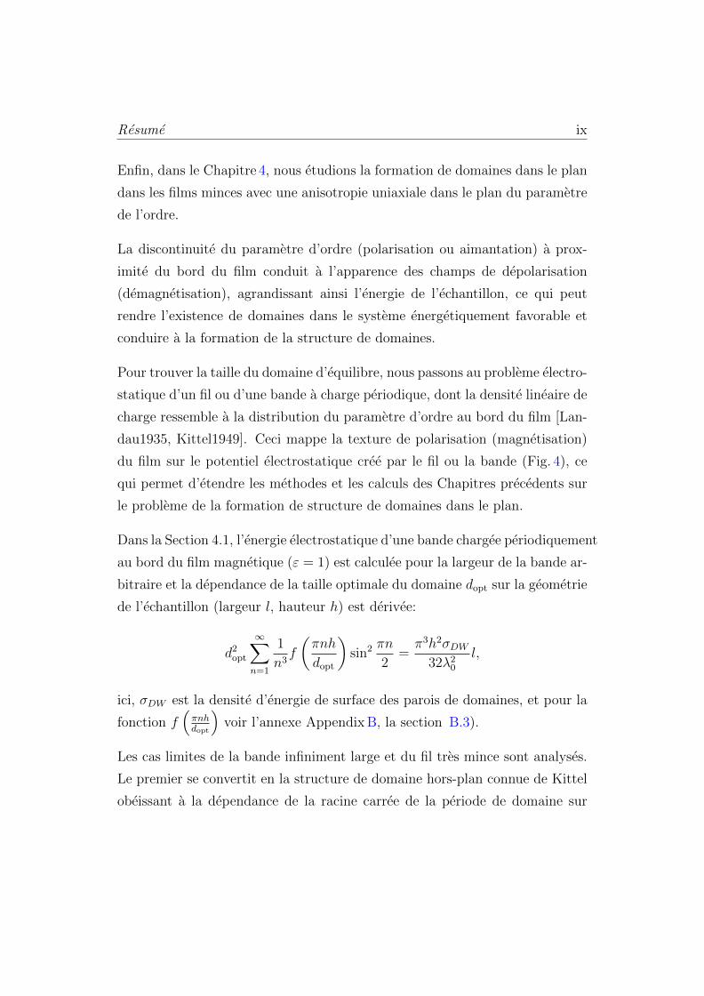
Pour trouver la taille du domaine d’equilibre, nous passons au probleme electro-
statique d’un fil ou d’une bande a charge periodique, dont la densite lineaire de
charge ressemble a la distribution du parametre d’ordre au bord du film [Lan-
dau1935, Kittel1949]. Ceci mappe la texture de polarisation (magnetisation)
du film sur le potentiel electrostatique cree par le fil ou la bande (Fig. 4), ce
qui permet d’etendre les methodes et les calculs des Chapitres precedents sur
le probleme de la formation de structure de domaines dans le plan.
Dans la Section 4.1, l’energie electrostatique d’une bande chargee periodiquement
au bord du film magnetique (ε = 1) est calculee pour la largeur de la bande ar-
bitraire et la dependance de la taille optimale du domaine dopt sur la geometrie
de l’echantillon (largeur l, hauteur h) est derivee:
d2opt
∞∑n=1
1
n3f
(πnh
dopt
)sin2 πn
2=π3h2σDW
32λ20
l,
ici, σDW est la densite d’energie de surface des parois de domaines, et pour la
fonction f(πnhdopt
)voir l’annexe Appendix B, la section B.3).
Les cas limites de la bande infiniment large et du fil tres mince sont analyses.
Le premier se convertit en la structure de domaine hors-plan connue de Kittel
obeissant a la dependance de la racine carree de la periode de domaine sur
Resume x
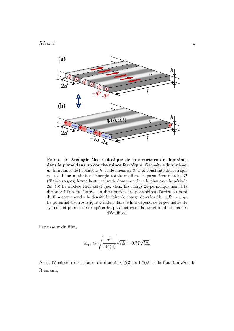
Figure 4: Analogie electrostatique de la structure de domainesdans le plane dans un couche mince ferroıque. Geometrie du systeme:un film mince de l’epaisseur h, taille lineaire l h et constante dielectriqueε. (a) Pour minimiser l’energie totale du film, le parametre d’ordre P(fleches rouges) forme la structure de domaines dans le plan avec la periode2d. (b) Le modele electrostatique: deux fils chargs 2d-periodiquement a ladistance l l’un de l’autre. La distribution des parametres d’ordre au borddu film correspond a la densite lineaire de charge dans les fils: ±P 7→ ±λ0.Le potentiel electrostatique ϕ induit dans le film depend de la geometrie dusysteme et permet de recuperer les parametres de la structure du domaines
d’equilibre.
l’epaisseur du film,
dopt '
√π2
14ζ(3)
√l∆ = 0.77
√l∆,
∆ est l’epaisseur de la paroi du domaine, ζ(3) ≈ 1.202 est la fonction zeta de
Riemann;
Resume xi
tandis que le deuxieme cas demontre la proportionnalite lineaire de la periode
de domaine sur la taille du film et la proportionnalite inverse de son epaisseur:
dopt '∆
2
l
h.
Une autre facon d’obtenir les domaines dans le plan dans les films minces est
de creer une paroi de domaine dans le materiau. Par exemple, la paroi chargee
de domaine, induite dans le DIPA-B ferroelectrique moleculaire par la pointe
du microscope a force piezoresponse [Lu2015], provoque l’apparition des tete-
a-tete (ou queue-a-queue, selon la charge de la paroi de domaine) domaines
dans le plan (Fig. 5 and Fig. 6).
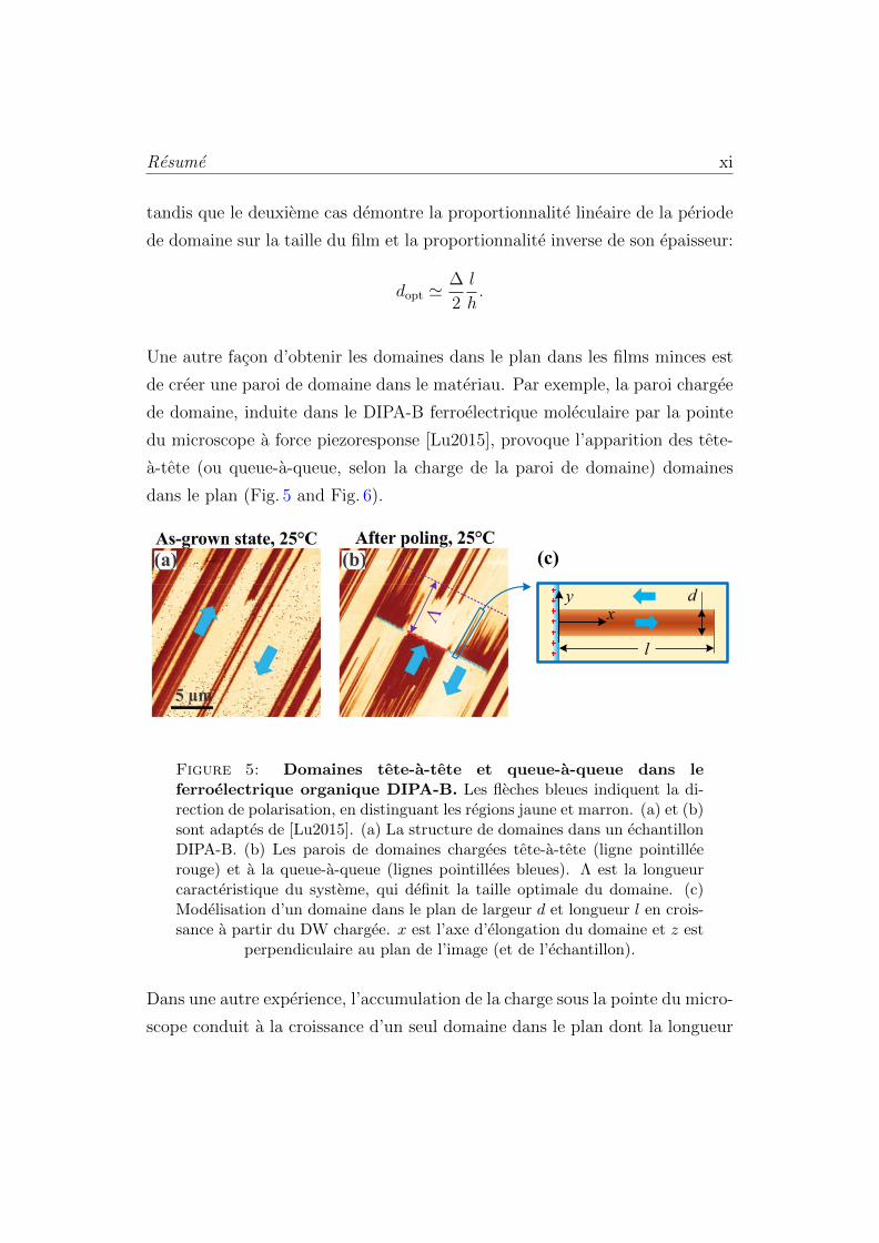
(c)
l
dx
y
Figure 5: Domaines tete-a-tete et queue-a-queue dans leferroelectrique organique DIPA-B. Les fleches bleues indiquent la di-rection de polarisation, en distinguant les regions jaune et marron. (a) et (b)sont adaptes de [Lu2015]. (a) La structure de domaines dans un echantillonDIPA-B. (b) Les parois de domaines chargees tete-a-tete (ligne pointilleerouge) et a la queue-a-queue (lignes pointillees bleues). Λ est la longueurcaracteristique du systeme, qui definit la taille optimale du domaine. (c)Modelisation d’un domaine dans le plan de largeur d et longueur l en crois-sance a partir du DW chargee. x est l’axe d’elongation du domaine et z est
perpendiculaire au plan de l’image (et de l’echantillon).
Dans une autre experience, l’accumulation de la charge sous la pointe du micro-
scope conduit a la croissance d’un seul domaine dans le plan dont la longueur
Resume xii
et la largeur dependent de la tension appliquee. Le travail de recherche ef-
fectue dans le Chapitre 4 contribue a la theorie des phenomenes discutes, en
particulier:
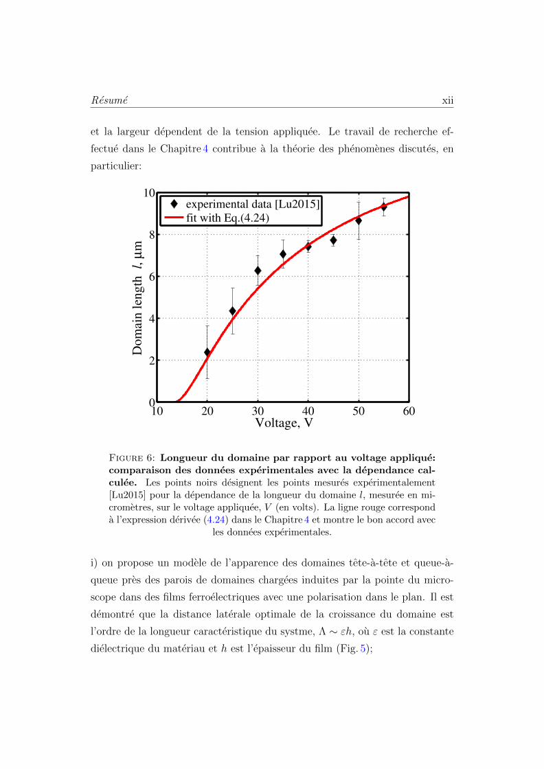
Voltage, V
Dom
ain l
ength
l,
µm
10 20 30 40 50 600
2
4
6
8
10experimental data [Lu2015]
fit with Eq.(4.24)
Figure 6: Longueur du domaine par rapport au voltage applique:comparaison des donnees experimentales avec la dependance cal-culee. Les points noirs designent les points mesures experimentalement[Lu2015] pour la dependance de la longueur du domaine l, mesuree en mi-crometres, sur le voltage appliquee, V (en volts). La ligne rouge corresponda l’expression derivee (4.24) dans le Chapitre 4 et montre le bon accord avec
les donnees experimentales.
i) on propose un modele de l’apparence des domaines tete-a-tete et queue-a-
queue pres des parois de domaines chargees induites par la pointe du micro-
scope dans des films ferroelectriques avec une polarisation dans le plan. Il est
demontre que la distance laterale optimale de la croissance du domaine est
l’ordre de la longueur caracteristique du systme, Λ ∼ εh, ou ε est la constante
dielectrique du materiau et h est l’epaisseur du film (Fig. 5);
Resume xiii
ii) l’expression de la dependance de la distance laterale de la croissance du
domaine l induite par la pointe du microscope sur le voltage applique V est
derivee,
V −1 = V −10 ln
[A
Λ√h√
−Φ−1 (l/Λ)+
1
2
],
demontrant le bon accord avec les donnees experimentales (Fig. 6). La fonction
Φ−1 est decrite dans l’annexe Appendix A.
Les expressions et le raisonnement de ce Chapitre peuvent etre utilises pour
d’autres etudes sur les structures de domaines dans des films ferroelectriques
et ferromagnetiques avec une anisotropie dans le plan du parametre d’ordre,
pour differentes geometries et differents parametres materiels.
Resume xiv
Bibliographie
[Abramowitz1965] Abramowitz, M. & Stegun, I. Handbook of Mathematical
Functions (Dover Publications, 1965).
[Baturina2013] Baturina, T. I. & Vinokur, V. M. Superinsulator–superconductor
duality in two dimensions. Annals of Physics 331, 236–257 (2013).
[Kittel1949] Kittel, C. Physical theory of ferromagnetic domains. Rev. Mod.
Phys., 21(4):541–583, 1949.
[Kondovych2017a] Kondovych, S., Luk’yanchuk, I., Baturina, T. I. & Vinokur,
V. M. Gate-tunable electron interaction in high-κ dielectric films. Sci. Rep.
7, 42770 (2017).
[Kondovych2017b] Kondovych, S. & Luk’yanchuk, I. Nondestructive method
of thin-film dielectric constant measurements by two-wire capacitor. Phys.
Status Solidi B 254, 1600476 (2017).
[Landau1935] Landau, L. D. and Lifshitz, E. M. On the theory of the dispersion
of magnetic permeability in ferromagnetic bodies. Phys. Z. Sowjet., 8(153):
101–114, 1935.
[Lu2015] Lu, H., Li, T., Poddar, S., Goit, O., Lipatov, A., Sinitskii, A.,
Ducharme, S., and Gruverman, A. Statics and Dynamics of Ferroelectric Do-
mains in Diisopropylammonium Bromide. Adv. Mater., 27(47):7832–7838,
2015.
[Rytova1967] Rytova, N. Screened potential of a point charge in the thin film.
Vestnik MSU (in Russian) 3, 30–37 (1967).
[Vendik1999] Vendik, O. G., Zubko, S. P. & Nikolskii, M. A. Modeling and
calculation of the capacitance of a planar capacitor containing a ferroelectric
thin film. Tech. Phys. 44, 349–355 (1999).
Contents
Abstract iii
Resume (en francais) iv
List of Figures xvii
Abbreviations xvii
Physical and Mathematical Constants xix
Symbols xx
1 Introduction: Charges in dielectric media 1
1.1 Charges in three dimensions . . . . . . . . . . . . . . . . . . . . 2
1.1.1 Where electrostatic begins . . . . . . . . . . . . . . . . . 2
1.1.2 Maxwell and Poisson equations . . . . . . . . . . . . . . 3
1.1.3 Electrostatic potential distribution . . . . . . . . . . . . 3
1.1.4 A charge inside a bulk dielectric . . . . . . . . . . . . . . 4
1.2 Charge interaction in dielectric thin film . . . . . . . . . . . . . 5
1.3 State of the art and objectives . . . . . . . . . . . . . . . . . . . 9
2 Charge confinement in high-κ dielectric films 13
2.1 Model: a point charge in a high-κ film . . . . . . . . . . . . . . 14
2.2 Electrostatic potential . . . . . . . . . . . . . . . . . . . . . . . 16
2.2.1 Numerical solution of Poisson equations . . . . . . . . . 16
2.2.2 Analytical solution and the interaction diagram . . . . . 18
xv
Contents xvi
2.2.3 A zoo of interaction regimes . . . . . . . . . . . . . . . . 20
2.3 Discussion and experimental outlook . . . . . . . . . . . . . . . 26
3 Extended linear charges in dielectric films 31
3.1 Capacitance measurement methods in thin dielectric films . . . 32
3.2 Electrostatics of a charged wire in a dielectric thin film . . . . . 34
3.3 Two-wire capacitance measurement . . . . . . . . . . . . . . . . 37
3.3.1 High-ε film, ε2 ≥ ε3 ε1 . . . . . . . . . . . . . . . . . . 39
3.3.2 Low-ε film, ε3 ≥ ε2 ε1 . . . . . . . . . . . . . . . . . . 41
3.4 Discussion and experimental outlook . . . . . . . . . . . . . . . 41
4 In-plane domains and domain walls in ferroic films 46
4.1 Periodic Kittel domain structure in thin ferroic films with in-plane anisotropy . . . . . . . . . . . . . . . . . . . . . . . . . . . 48
4.1.1 In-plane 180 stripe domains: geometry and model . . . 48
4.1.2 General expression for the electrostatic energy of the pe-riodically charged stripe . . . . . . . . . . . . . . . . . . 51
4.1.3 Optimal domain size . . . . . . . . . . . . . . . . . . . . 53
4.1.3.1 Wide charged edge: transition to the Kittel’sproblem . . . . . . . . . . . . . . . . . . . . . . 54
4.1.3.2 Narrow charged edge: in-plane domains in thinfilm . . . . . . . . . . . . . . . . . . . . . . . . 55
4.2 In-plane domain structure in an organic ferroelectric DIPA-B . . 58
4.2.1 Model of the striped domains in DIPA-B . . . . . . . . . 59
4.2.2 Electrostatic energy and domain growth distance . . . . 61
4.3 Creation of a single in-plane domain in DIPA-B organic ferro-electric . . . . . . . . . . . . . . . . . . . . . . . . . . . . . . . . 64
4.4 Discussion and experimental outlook . . . . . . . . . . . . . . . 68
Conclusions and main results 74
A Properties of the function Φn(z) 77
B Optimal domain size in the in-plane domain structure 81
B.1 Electrostatic energy derivation . . . . . . . . . . . . . . . . . . . 81
B.2 Analysis of the integral expressions . . . . . . . . . . . . . . . . 83
B.3 Total energy minimization and the optimal domain size . . . . . 86
List of Figures
1.1 Charged particle in the middle of a three-layer dielectric structure 5
1.2 Asymptotic behaviour of the potential . . . . . . . . . . . . . . 8
2.1 Gate-controlled charge interaction in a high-κ film: system ge-ometry . . . . . . . . . . . . . . . . . . . . . . . . . . . . . . . . 15
2.2 Electrostatic potential distribution in a high-κ film . . . . . . . 17
2.3 Spatial distribution of the potential and electric field lines . . . 18
2.4 Electrostatic potential in the presence of the gate . . . . . . . . 21
2.5 The square root law for the gate-dependent screening length . . 22
2.6 Sketch of the regimes of electrostatic interactions . . . . . . . . 25
3.1 Model of a two-wire capacitor . . . . . . . . . . . . . . . . . . . 35
3.2 Spatial distribution of the electrostatic potential for a two-wiresystem . . . . . . . . . . . . . . . . . . . . . . . . . . . . . . . . 36
3.3 Auxiliary trigonometric integral function g(ξ) . . . . . . . . . . 38
3.4 Dependence of the capacitance on the distance between thewires for various values of dielectric constants . . . . . . . . . . 40
3.5 Determination of the dielectric constant of the low-ε film . . . . 42
4.1 Electrostatic mapping of the in-plane stripe domain structurein a ferroic thin film . . . . . . . . . . . . . . . . . . . . . . . . 49
4.2 Periodically charged linear systems . . . . . . . . . . . . . . . . 51
4.3 Meijer G-function and its asymptotes . . . . . . . . . . . . . . . 53
4.4 Head-to-head and tail-to-tail in-plane domains . . . . . . . . . . 58
4.5 Estimation of the optimal domain length . . . . . . . . . . . . . 62
4.6 Modeling of the tip-induced in-plane domains in DIPA-B . . . . 64
4.7 Domain length vs. applied voltage: fitting the experimental data 68
xvii
Abbreviations
AFM Antiferromagnetic
BC Boundary Condition
BKT Berezinskii-Kosterlitz-Thouless (transition)
CDW Charged Domain Wall
CTM Charge-trapping Memory
DIPA-B Diisopropylammonium bromide
DW Domain Wall
FE Ferroelectric
FM Ferromagnetic
PFM Piezoresponse Force Microscopy
SI Systeme International d’unites, The International System of Units
SGS The Centimetre-Gram-Second system of units
xviii
Physical and Mathematical
Constants
Euler’s constant γ ≈ 0.577
Exponent of the Euler’s constant eγ = c ≈ 1.781
Vacuum permittivity ε0 ≈ 8.854 ×10¹² F/m
Riemann zeta function ζ(2) = π2/6 ≈ 1.645
ζ(3) ≈ 1.202
xix
Symbols
(ρ, θ, z) the cylindrical coordinates m
(x, y, z) the Cartesian coordinates m
a, h, d, l geometric parameters, distances m
α small cutoff parameter m
Λ the characteristic electrostatic screening length m
ε, κ dielectric permeability (dielectric constant)
ϕ, φ electrostatic potential V
e, q charge C
U electrostatic interaction energy J
C capacitance F
η anisotropy factor (of dielectric permeability)
P order parameter
P electric polarization C/m2
M magnetization A/m
λ, ql linear charge density C/m
E electric field V/m
F ,Ftotal (total) energy density J/m
Fel electrostatic energy density J/m
FDW domain wall energy density J/m
xx
Symbols xxi
σDW domain wall surface tension J/m2
dopt optimal (equilibrium) domain width m
∆ domain wall thickness m
V voltage V
n,m, ν indices, integer numbers
k Fourrier transform variable 1/m
δn the n-dimensional Dirac delta-function m−n
f, g auxiliary trigonometric integral functions
Jν Bessel function of order ν
Hν Struve function of order ν
Nν Neumann function of order ν
Kν Macdonald function of order ν
Φν difference of Struve and Neumann functions
G,G Meijer G-function
ζ Riemann zeta function
Chapter 1
Introduction: Charges in
dielectric media
Electrostatics is one of the pillars of natural sciences. Its role can’t be overesti-
mated, as it deals with one of four existing interaction types, the electrostatic
interaction, that is crucial for the existence of matter itself.
In spite of the long history of the electrostatics, still, there are many unexplored
questions related to it. One of them arised recently, with the beginning of the
era of nanotechnology, when it appeared that properties of thin films and other
meso- and nanoobjects differ from those in the bulk, and the question is, – how
exactly they are different. Large variety of phenomena connected to the small
size and low dimensionality of the meso- and nanosystems has been observed
and explained; many others, though obtained in the experiments, still are not
fully understood and need detailed theoretical investigation. Starting with the
basic brick of electrostatics, the electrostatic interaction between charges, my
hope is to get closer to this understanding.
1
I. Introduction: Charges in dielectric media 2
1.1 Charges in three dimensions
1.1.1 Where electrostatic begins
The electrostatic interaction force between two stationery point charges q1
(located in a point of space with the radius vector r1) and q2 (located in r2)
in a vacuum obeys the Coulomb’s law,
F = kq1q2r2 − r1
|r2 − r1|3, (1.1)
where k is a constant that depends on the chosen system of units (e.g. k = 1
in the SGS units, k = (4πε0)−1 in the SI units, ε0 is the vacuum permittivity).
In this Thesis, we work within the SI system of measurement.
For a huge set of problems, the expression (1.1) is a primary means to model
and describe the electrostatic phenomena. For the simplest case of one charge
q, placed in the origin of the coordinate system, the electric field related to it,
is a force that a test charge located in r experiences,
E = kqr
|r|3. (1.2)
When it comes to a number of charges interacting in vacuum, distributed
with the spatial density qΩ in the volume Ω, we can apply the superposition
principle, in order to determine the force acting on a probe charge:
E(r) = k
∫Ω
qΩ(r′)r − r′
|r − r′|3d3r′. (1.3)
Such summation appears to be quite complicated mathematically, except for
a few well-known problems with simple geometry and homogeneous charge
distribution. In a real material, one should take into account the interaction
between all the particles, which is often hard to solve even numerically. How-
ever, there are several analytical tools of electrostatics that might help.
I. Introduction: Charges in dielectric media 3
1.1.2 Maxwell and Poisson equations
In the electrostatic approximation, the electric field satisfies the following
Maxwell’s equations (in the differential form):
divE = 4πkqΩ, rotE = 0. (1.4)
The first is called the Maxwell-Gauss equation. The second, Maxwell-Faraday
equation, shows that the electric field is irrotational, thus the gradient exists:
E = −∇ϕ. (1.5)
Combined with the first equation in (1.4), it provides the relation between the
potential and the charge density: the Poisson’s equation (or Laplace equation,
if qΩ = 0).
∇2ϕ = −4πkqΩ. (1.6)
1.1.3 Electrostatic potential distribution
Recovering the solution of the Poisson’s equation (1.6), thus determining the
electric field (or potential) in every point of space given the spatial density
of the distributed free charge (on the surface of conductors) constitute the
main problem of electrostatics. The uniqueness theorem for Poisson’s equation
claims, that once the function for the potential is found (up to a constant) and
it satisfies the requirements of the continuity and smoothness, which are often
referred to as boundary conditions, that is the right and unique solution. This
fact generated the variety of analytical methods for obtaining the potential
distribution in a given system, among which:
– the Fourier transform method, the Wiener-Hopf method, and other mathe-
matical methods for solving the differential equations;
I. Introduction: Charges in dielectric media 4
– the method of images;
– the conformal mapping techniques;
– simple guess; and others.
The Poisson’s equation may be as well solved numerically in many cases.
1.1.4 A charge inside a bulk dielectric
Now, let us put a point charge in an infinite bulk dielectric material. The elec-
tric field induced by the charge causes dielectric polarization in the material:
positive charges shift toward the field, while negative charges shift oppositely.
The density of created dipole moments is called the electric polarization and
is usually denoted as P.
The polarizability of the material, i.e. the measure of how easily it polarizes
in the electric field, is determined by the dielectric susceptibility χ, which is a
tensor in general case of anisotropic material: P = ε0χE.
In its turn, χ determines the dielectric permeability (dielectric constant) ε =
χ+ 1. In the isotropic case, this remarkable characteristic of the dielectric ma-
terial simply lowers the electric field by ε times. Thus, the Poisson’s equation
inside the isotropic dielectric will acquire the form:
∇2ϕ = −4πk
εqΩ,
and its solution for the case of a point charge q in an infinite 3D bulk dielectric:
ϕ =kq
εr; E =
kq
ε
r
|r|3.
In the following Section it is discussed, how this ∝ 1/r behavior of the elec-
trostatic potential changes when the charge is placed in a thin dielectric film
instead of the bulk.
I. Introduction: Charges in dielectric media 5
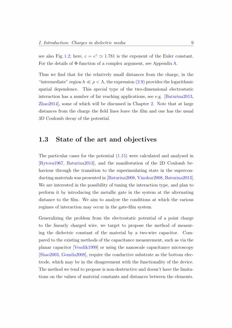
1.2 Charge interaction in dielectric thin film
qh
ε1
ε2
ε3
ρ
z
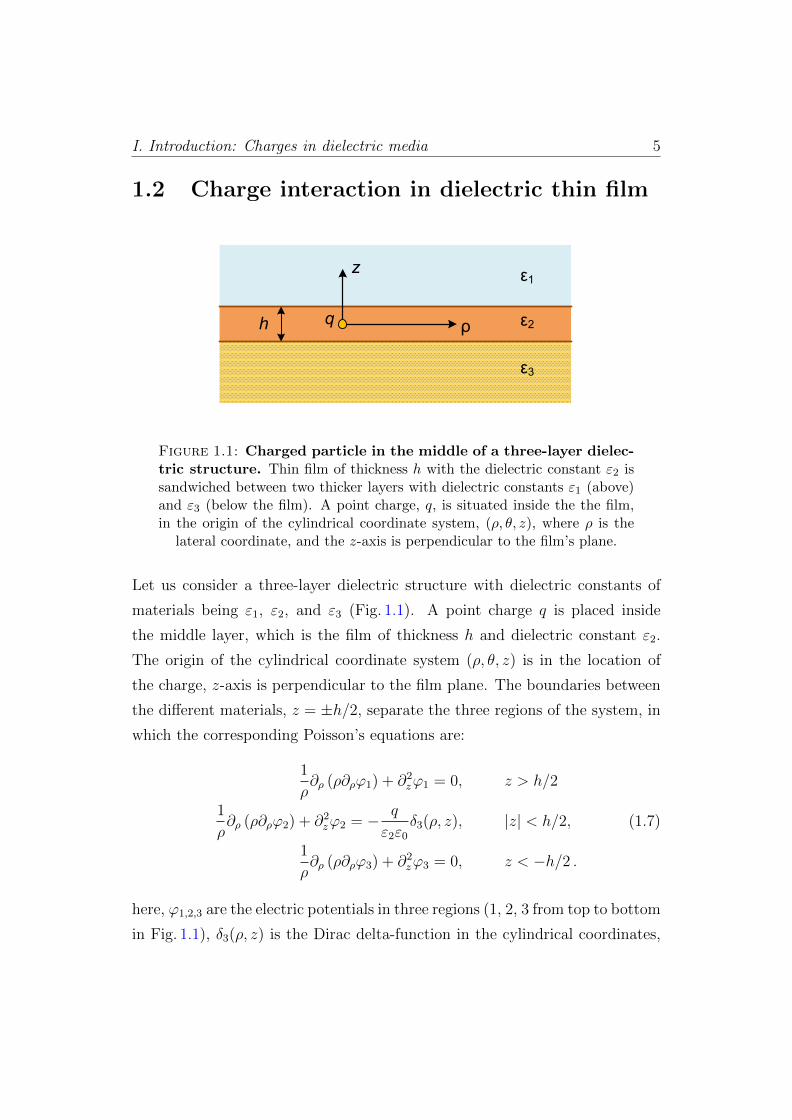
Figure 1.1: Charged particle in the middle of a three-layer dielec-tric structure. Thin film of thickness h with the dielectric constant ε2 issandwiched between two thicker layers with dielectric constants ε1 (above)and ε3 (below the film). A point charge, q, is situated inside the the film,in the origin of the cylindrical coordinate system, (ρ, θ, z), where ρ is the
lateral coordinate, and the z-axis is perpendicular to the film’s plane.
Let us consider a three-layer dielectric structure with dielectric constants of
materials being ε1, ε2, and ε3 (Fig. 1.1). A point charge q is placed inside
the middle layer, which is the film of thickness h and dielectric constant ε2.
The origin of the cylindrical coordinate system (ρ, θ, z) is in the location of
the charge, z-axis is perpendicular to the film plane. The boundaries between
the different materials, z = ±h/2, separate the three regions of the system, in
which the corresponding Poisson’s equations are:
1
ρ∂ρ (ρ∂ρϕ1) + ∂2
zϕ1 = 0, z > h/2
1
ρ∂ρ (ρ∂ρϕ2) + ∂2
zϕ2 = − q
ε2ε0
δ3(ρ, z), |z| < h/2, (1.7)
1
ρ∂ρ (ρ∂ρϕ3) + ∂2
zϕ3 = 0, z < −h/2 .
here, ϕ1,2,3 are the electric potentials in three regions (1, 2, 3 from top to bottom
in Fig. 1.1), δ3(ρ, z) is the Dirac delta-function in the cylindrical coordinates,
I. Introduction: Charges in dielectric media 6
ε0 is the vacuum permittivity (we work in the SI units from now on). The
boundary conditions at the material interfaces (z = ±h/2) are:
ϕ1 = ϕ2; ε2∂zϕ2 = ε1∂zϕ1, z = +h/2, (1.8)
ϕ2 = ϕ3; ε2∂zϕ2 = ε3∂zϕ3, z = −h/2 .
We look for the solution of equations (1.7) in the form:
ϕ1 =
∞∫0
A1e−kzJ0 (kρ) dk; (1.9)
ϕ2 =q
4πε0ε2
∞∫0
e−k|z|J0 (kρ) dk +
∞∫0
B1e−kzJ0 (kρ) dk +
∞∫0
B2ekzJ0 (kρ) dk;
ϕ3 =
∞∫0
A2ekzJ0 (kρ) dk.
Here, J0 is the zero order Bessel function. Applying the boundary conditions
(1.8), we obtain the set of four linear equations. Solving them gives us the
unknown coefficients A1 (k) , A2 (k) , B1 (k) , B2 (k). Since we are interested in
the potential ϕ2 inside the film, the coefficients we need:
B1 = − q
4πε0ε2
β3
(β1 + ekh
)β1β3 − e2kh
, B2 = − q
4πε0ε2
β1
(β3 + ekh
)β1β3 − e2kh
, (1.10)
with
β1 =1− ε1/ε2
1 + ε1/ε2
and β3 =1− ε3/ε2
1 + ε3/ε2
. (1.11)
Then, the potential inside the film reads as:
ϕ2 = − q
4πε0ε2
∞∫0
[−e−k|z| +
β3
(β1 + ekh
)β1β3 − e2kh
e−kz +β1
(β3 + ekh
)β1β3 − e2kh
ekz
]J0 (kρ) dk.
(1.12)
I. Introduction: Charges in dielectric media 7
Employing the sum of a geometric series and using the following table integral
[Gradshteyn2014],∞∫
0
e−pxJ0 (bx) dx =1√
p2 + b2,
we can find the solution in the following form:
ϕ2 =q
4πε0ε2
1√ρ2 + z2
+ (1.13)
+q
4πε0ε2
[Ξ(2h+ z) + Ξ(2h− z) +
1
β1
Ξ(h+ z) +1
β3
Ξ(h− z)
],
where
Ξ(ξ) =∞∑m=0
(β1β3)m+1√ρ2 + (2mh+ ξ)2
(1.14)
Albeit the expression (1.14) gives the exact formula for the electrostatic poten-
tial induced by a point charge in thin film, it needs some further simplifications
to extract the peculiar features of the potential behaviour at various distances.
First, we argue that the distance between interacting free charges in a film is
much larger than the film thickness, ρ h. This allows to neglect the depen-
dence on z coordinate (we take z = 0), and to expand the integral expression
(1.12) over the small parameter kh 1:
ϕ2(ρ) =1
4πε0
2q
ε1 + ε3
∞∫0
J0 (kρ)
kΛ + 1dk, (1.15)
where the characteristic length of the system, Λ, is introduced:
Λ =(ε2 + ε1) (ε2 + ε3)
ε2 (ε1 + ε3)h. (1.16)
Hereupon the potential can be easily integrated:
ϕ2(ρ) =qΛ−1
4ε0(ε1 + ε3)
[H0
( ρΛ
)− Y0
( ρΛ
)]. (1.17)
I. Introduction: Charges in dielectric media 8
The similar result for the potential at ρ h, but for the particular case of ε1 =
ε3 and ε2 ε1,3 was obtained in [Rytova1967]. Here, H0 (x) and N0 (x) are
the zero order Struve and Neumann functions, respectively [Abramowitz1965].
Since this difference of two special functions will often appear while solving 2D
electrostatic problems, it is reasonable to establish the notation:
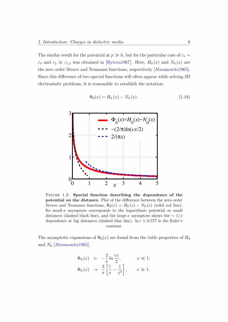
Φ0(x) = H0 (x)−N0 (x) . (1.18)
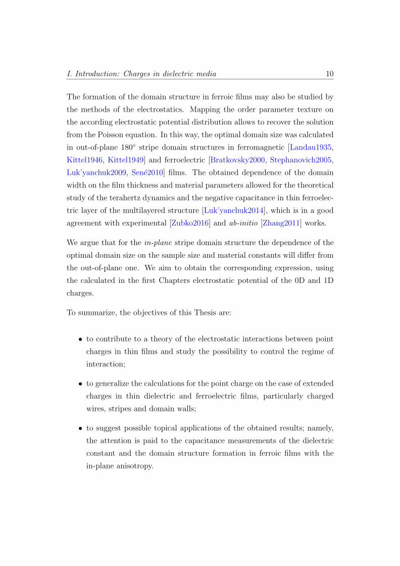
x
0 1 2 3 4 50
1
2
3 Φ
0(x)=H
0(x)−N
0(x)
−(2/π)ln(cx/2)
2/(πx)
Figure 1.2: Special function describing the dependence of thepotential on the distance. Plot of the difference between the zero orderStruve and Neumann functions, Φ0(x) = H0 (x) − N0 (x) (solid red line).Its small-x asymptote corresponds to the logarithmic potential at smalldistances (dashed black line), and the large-x asymptote shows the ∼ 1/xdependence at big distances (dashed blue line). ln c ' 0.577 is the Euler’s
constant.
The asymptotic expansions of Φ0(x) are found from the table properties of H0
and N0 [Abramowitz1965],
Φ0 (x) ' − 2
πlncx
2, x 1;
Φ0 (x) → 2
π
[1
x− 1
x3
], x 1.
I. Introduction: Charges in dielectric media 9
see also Fig. 1.2; here, c = eγ ' 1.781 is the exponent of the Euler constant.
For the details of Φ-function of a complex argument, see Appendix A.
Thus we find that for the relatively small distances from the charge, in the
“intermediate” region h ρ < Λ, the expression (2.9) provides the logarithmic
spatial dependence. This special type of the two-dimensional electrostatic
interaction has a number of far reaching applications, see e.g. [Baturina2013,
Zhao2014], some of which will be discussed in Chapter 2. Note that at large
distances from the charge the field lines leave the film and one has the usual
3D Coulomb decay of the potential.
1.3 State of the art and objectives
The particular cases for the potential (1.15) were calculated and analyzed in
[Rytova1967, Baturina2013], and the manifestation of the 2D Coulomb be-
haviour through the transition to the superinsulating state in the supercon-
ducting materials was presented in [Baturina2008, Vinokur2008, Baturina2013].
We are interested in the possibility of tuning the interaction type, and plan to
perform it by introducing the metallic gate in the system at the alternating
distance to the film. We aim to analyze the conditions at which the various
regimes of interaction may occur in the gate-film system.
Generalizing the problem from the electrostatic potential of a point charge
to the linearly charged wire, we target to propose the method of measur-
ing the dielectric constant of the material by a two-wire capacitor. Com-
pared to the existing methods of the capacitance measurement, such as via the
planar capacitor [Vendik1999] or using the nanoscale capacitance microscopy
[Shao2003, Gomila2008], require the conductive substrate as the bottom elec-
trode, which may be in the disagreement with the functionality of the device.
The method we tend to propose is non-destructive and doesn’t have the limita-
tions on the values of material constants and distances between the elements.
I. Introduction: Charges in dielectric media 10
The formation of the domain structure in ferroic films may also be studied by
the methods of the electrostatics. Mapping the order parameter texture on
the according electrostatic potential distribution allows to recover the solution
from the Poisson equation. In this way, the optimal domain size was calculated
in out-of-plane 180 stripe domain structures in ferromagnetic [Landau1935,
Kittel1946, Kittel1949] and ferroelectric [Bratkovsky2000, Stephanovich2005,
Luk’yanchuk2009, Sene2010] films. The obtained dependence of the domain
width on the film thickness and material parameters allowed for the theoretical
study of the terahertz dynamics and the negative capacitance in thin ferroelec-
tric layer of the multilayered structure [Luk’yanchuk2014], which is in a good
agreement with experimental [Zubko2016] and ab-initio [Zhang2011] works.
We argue that for the in-plane stripe domain structure the dependence of the
optimal domain size on the sample size and material constants will differ from
the out-of-plane one. We aim to obtain the corresponding expression, using
the calculated in the first Chapters electrostatic potential of the 0D and 1D
charges.
To summarize, the objectives of this Thesis are:
• to contribute to a theory of the electrostatic interactions between point
charges in thin films and study the possibility to control the regime of
interaction;
• to generalize the calculations for the point charge on the case of extended
charges in thin dielectric and ferroelectric films, particularly charged
wires, stripes and domain walls;
• to suggest possible topical applications of the obtained results; namely,
the attention is paid to the capacitance measurements of the dielectric
constant and the domain structure formation in ferroic films with the
in-plane anisotropy.
Bibliography
[Abramowitz1965] Abramowitz, M. & Stegun, I. Handbook of Mathematical
Functions (Dover Publications, 1965).
[Baturina2008] Baturina, T. I. et al. Hyperactivated resistance in TiN films on
the insulating side of the disorder-driven superconductor-insulator transi-
tion. JETP Lett. 88, 752–757 (2008).
[Baturina2013] Baturina, T. I. & Vinokur, V. M. Superinsulator–supercon-
ductor duality in two dimensions. Annals of Physics 331, 236–257 (2013).
[Bratkovsky2000] Bratkovsky, A. M. & Levanyuk, A. P. Abrupt Appearance
of the Domain Pattern and Fatigue of Thin Ferroelectric Films. Phys.
Rev. Lett. 84, 3177 (2000).
[Gomila2008] Gomila, G., Toset, J. & Fumagalli, L. Nanoscale capacitance
microscopy of thin dielectric films. J. Appl. Phys. 104, 024315 (2008).
[Gradshteyn2014] Gradshteyn, I. S. & Ryzhik, I. M. Table of integrals, series,
and products (Academic press, 2014).
[Kittel1946] Kittel, C. Theory of the structure of ferromagnetic domains in
films and small particles. Phys. Rev. 70(11-12), 965–971 (1946).
[Kittel1949] Kittel, C. Physical theory of ferromagnetic domains. Rev. Mod.
Phys. 21(4), 541–583 (1949).
[Landau1935] Landau, L. D. and Lifshitz, E. M. On the theory of the disper-
sion of magnetic permeability in ferromagnetic bodies. Phys. Z. Sowjet.
8, 101–114 (1935).
11
I. Introduction: Charges in dielectric media 12
[Luk’yanchuk2009] Luk’yanchuk, I. A., Lahoche, L., and Sene, A. Universal
properties of ferroelectric domains. Phys. Rev. Lett. 102, 147601 (2009).
[Luk’yanchuk2014] Luk’yanchuk, I., Pakhomov, A., Sene, A., Sidorkin, A.,
and Vinokur, V. Terahertz Electrodynamics of 180 Domain Walls in
Thin Ferroelectric Films. https://arxiv.org/abs/1410.3124, 2014.
[Rytova1967] Rytova, N. Screened potential of a point charge in the thin film.
Vestnik MSU (in Russian) 3, 30–37 (1967).
[Sene2010] Sene, A. Theory of Domains and Nonuniform Textures in Ferro-
electrics. (University of Picardie Jules Verne, PhD thesis edition, 2010).
[Shao2003] Shao, R., Kalinin, S. V. & Bonnell, D. A. Local impedance imag-
ing and spectroscopy of polycrystalline ZnO using contact atomic force
microscopy. Appl. Phys. Lett. 82, 1869–1871 (2003).
[Stephanovich2005] Stephanovich, V. A., Lukyanchuk, I. A. & Karkut, M. G.
Domain-Enhanced Interlayer Coupling in Ferroelectric/ Paraelectric Su-
perlattices. Phys. Rev. Lett. 94, 047601 (2005).
[Vendik1999] Vendik, O. G., Zubko, S. P. & Nikolskii, M. A. Modeling and cal-
culation of the capacitance of a planar capacitor containing a ferroelectric
thin film. Tech. Phys. 44, 349–355 (1999).
[Vinokur2008] Vinokur, V. M. et al. Superinsulator and quantum synchro-
nization. Nature 452, 613–615 (2008).
[Zubko2016] Zubko, P. et al. Negative capacitance in multidomain ferroelectric
superlattices. Nature 534(7608), 524–528 (2016).
[Zhao2014] Zhao, C., Zhao, C. Z., Taylor, S. & Chalker, P. R. Review on
non-volatile memory with high-k dielectrics: flash for generation beyond
32 nm. Materials 7, 5117–5145 (2014).
[Zhang2011] Zhang, Q., Herchig, R., and Ponomareva, I. Nanodynamics of
Ferroelectric Ultrathin Films. Phys. Rev. Lett., 107(17), 2011.
Chapter 2
Charge confinement in high-κ
dielectric films
Dielectric thin films with the high value of dielectric constant are often referred
to as “high-κ” thin films and attract intense experimental and theoretical at-
tention, see Ref. [Osada2012] and references therein. Following this established
term, the notation of the dielectric constant (dielectric permeability) in this
Chapter is replaced by “κ” instead of traditional notation, “ε”, which is used
in the rest of the Thesis, while both relate to the same physical quantity.
The interest to high-κ 2D systems is motivated by their high technological
perspective for design and fabrication of nanoscale devices. They cover a
wide spectrum of physical systems [Baturina2013, Castner1975, Grannan1981,
Hess1982, Yakimov1997, Watanabe2000] ranging from traditional dielectrics
and ferroelectrics to strongly disordered thin metallic and superconducting
films experiencing metal-insulator and superconductor-insulator transitions,
respectively.
The major feature of high-κ systems leading to their unique properties, is that
the electric field induced by the trapped charge remains confined within the
13
II. Charge confinement in high-κ dielectric films 14
film. This ensures the electrostatic integrity and stability with respect to ex-
ternal perturbations and gives rise to the 2D character of the Coulomb interac-
tions between the charges [Rytova1967, Chaplik1972, Keldysh1979]. Namely,
the potential produced by the charge, located inside the high-κ sheet of thick-
ness h, sandwiched between media with κa and κb permeabilities, exhibits the
logarithmic distance dependence, ϕ(ρ) ∝ ln(ρ/Λ), extending till the funda-
mental screening length of the potential dimensional crossover (1.16), which in
the notations of this Chapter is written as
Λ =κh
κa + κb. (2.1)
The screening length, Λ, is a major parameter controlling the electric properties
of the high-κ films. Thus, their applications require reliable and simple ways
of tuning Λ which, at the same time, maintain robustness of the underlying
dielectric properties of the system. As it is shown below, this is achieved by the
clever location of the control gate. Adjusting the distance between the high-κ
film and the gate, we vary the screening length of the logarithmic interaction
and obtain a wealth of the electrostatic behaviors at different spatial scales,
enabling to control the scalability and capacitance of the system. In what
follows we describe the electrostatic properties of the generic high-κ device
with the tunable distance to the control gate.
2.1 Model: a point charge in a high-κ film
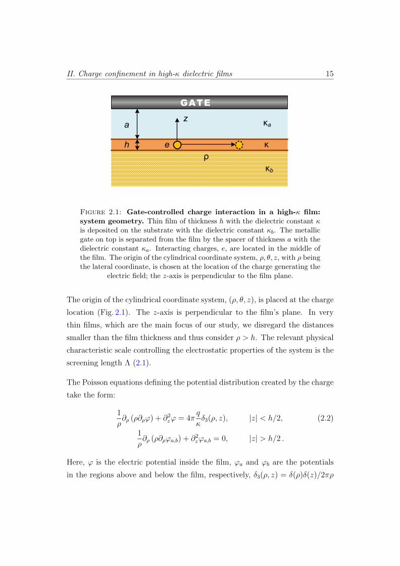
The geometry of the system is presented in Fig. 2.1. A point charge, e < 0,
is located inside a high-κ film of the thickness h, deposited on a dielectric
substrate with the dielectric constant κb. Above the film, there is a metallic
gate, which is separated from the film by a layer of the thickness a with the
dielectric constant κa.
II. Charge confinement in high-κ dielectric films 15
h
κa
κ
κb
ρ
a
GATE
e
z
Figure 2.1: Gate-controlled charge interaction in a high-κ film:system geometry. Thin film of thickness h with the dielectric constant κis deposited on the substrate with the dielectric constant κb. The metallicgate on top is separated from the film by the spacer of thickness a with thedielectric constant κa. Interacting charges, e, are located in the middle ofthe film. The origin of the cylindrical coordinate system, ρ, θ, z, with ρ beingthe lateral coordinate, is chosen at the location of the charge generating the
electric field; the z-axis is perpendicular to the film plane.
The origin of the cylindrical coordinate system, (ρ, θ, z), is placed at the charge
location (Fig. 2.1). The z-axis is perpendicular to the film’s plane. In very
thin films, which are the main focus of our study, we disregard the distances
smaller than the film thickness and thus consider ρ > h. The relevant physical
characteristic scale controlling the electrostatic properties of the system is the
screening length Λ (2.1).
The Poisson equations defining the potential distribution created by the charge
take the form:
1
ρ∂ρ (ρ∂ρϕ) + ∂2
zϕ = 4πq
κδ3(ρ, z), |z| < h/2, (2.2)
1
ρ∂ρ (ρ∂ρϕa,b) + ∂2
zϕa,b = 0, |z| > h/2 .
Here, ϕ is the electric potential inside the film, ϕa and ϕb are the potentials
in the regions above and below the film, respectively, δ3(ρ, z) = δ(ρ)δ(z)/2πρ
II. Charge confinement in high-κ dielectric films 16
is the 3D Dirac delta-function in the cylindrical coordinates, q = e and q =
e/4πε0 in CGS and SI systems respectively, ε0 is the vacuum permittivity (for
simplicity, the notation from Chapter 1, q/(4πε0), is replaced by q here). The
electrostatic boundary conditions at the film surfaces (z = ±h/2) are:
ϕ = ϕa; κ∂zϕ = κa∂zϕa, z = +h/2, (2.3)
ϕ = ϕb; κ∂zϕ = κb∂zϕb, z = −h/2 ,
and ϕa = 0 at z = a+ h/2 at the interface with the electrode.
Then, the energy of the interaction with the second identical electron located
at the distance ρ (see Fig. 2.1, the test electron is shown by a dashed circle) is
given by U (ρ) = 2eϕ (ρ). For numerical calculations we use typical values of
parameters for a InO film deposited on the SiO2 substrate [Baturina2013]: the
film dielectric constant, κ ' 104, the substrate dielectric constant, κb = 4, and
the dielectric constant for the air gap between the film and the gate, κa = 1.
2.2 Electrostatic potential
2.2.1 Numerical solution of Poisson equations
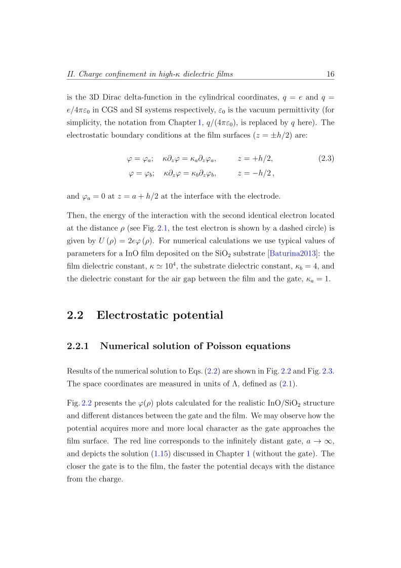
Results of the numerical solution to Eqs. (2.2) are shown in Fig. 2.2 and Fig. 2.3.
The space coordinates are measured in units of Λ, defined as (2.1).
Fig. 2.2 presents the ϕ(ρ) plots calculated for the realistic InO/SiO2 structure
and different distances between the gate and the film. We may observe how the
potential acquires more and more local character as the gate approaches the
film surface. The red line corresponds to the infinitely distant gate, a → ∞,
and depicts the solution (1.15) discussed in Chapter 1 (without the gate). The
closer the gate is to the film, the faster the potential decays with the distance
from the charge.
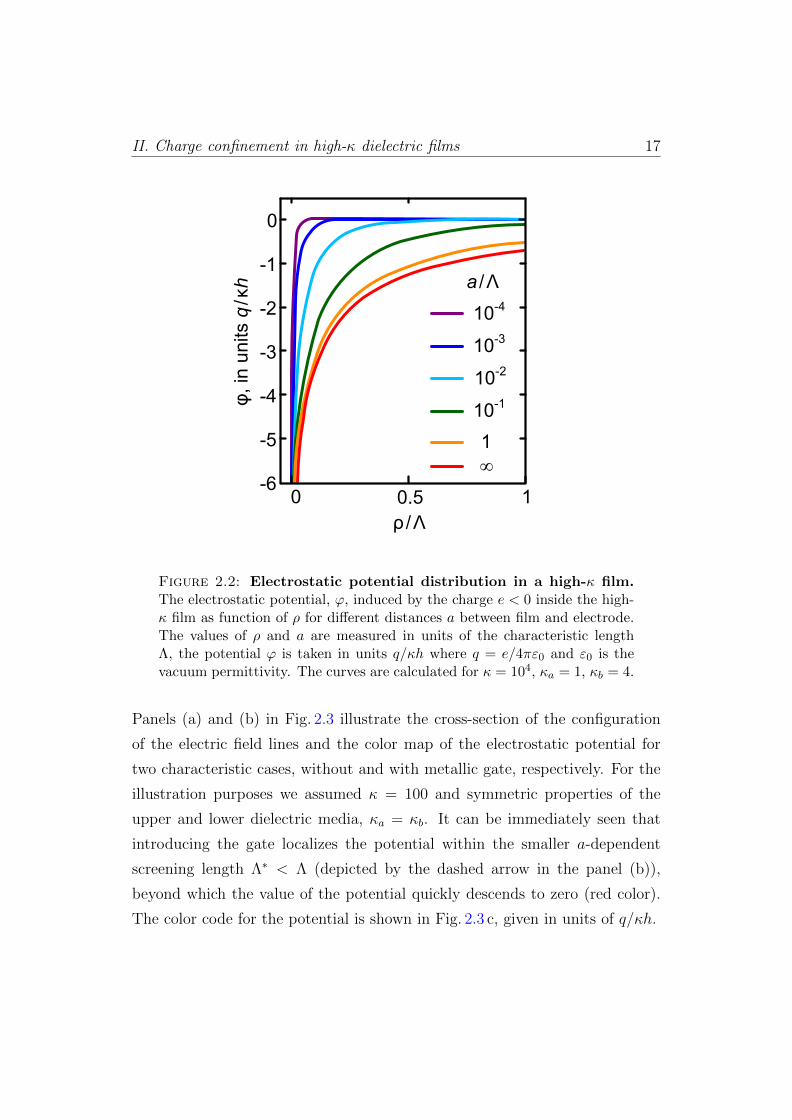
II. Charge confinement in high-κ dielectric films 17
-6
-5
-4
-3
-2
-1
0
ρ/Λ
φ, i
n un
its q
/κh
0 0.5 1
a /Λ
10-4
10-3
10-2
10-1
1
Figure 2.2: Electrostatic potential distribution in a high-κ film.The electrostatic potential, ϕ, induced by the charge e < 0 inside the high-κ film as function of ρ for different distances a between film and electrode.The values of ρ and a are measured in units of the characteristic lengthΛ, the potential ϕ is taken in units q/κh where q = e/4πε0 and ε0 is thevacuum permittivity. The curves are calculated for κ = 104, κa = 1, κb = 4.
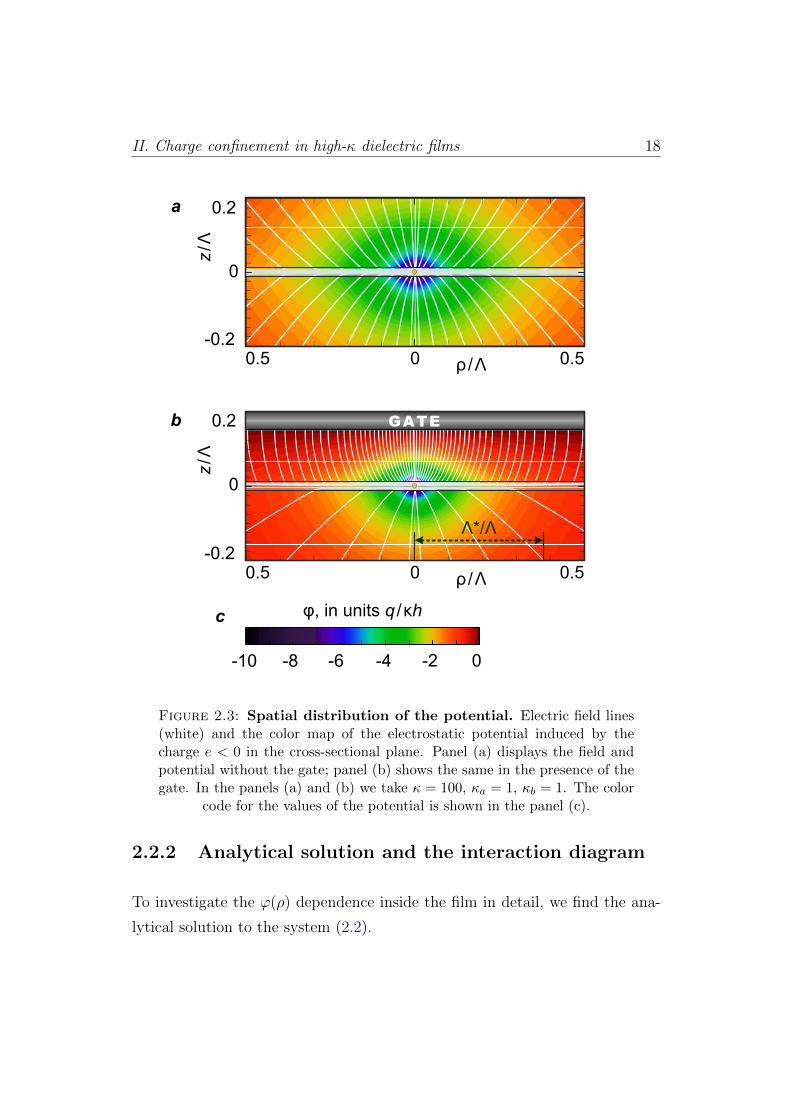
Panels (a) and (b) in Fig. 2.3 illustrate the cross-section of the configuration
of the electric field lines and the color map of the electrostatic potential for
two characteristic cases, without and with metallic gate, respectively. For the
illustration purposes we assumed κ = 100 and symmetric properties of the
upper and lower dielectric media, κa = κb. It can be immediately seen that
introducing the gate localizes the potential within the smaller a-dependent
screening length Λ∗ < Λ (depicted by the dashed arrow in the panel (b)),
beyond which the value of the potential quickly descends to zero (red color).
The color code for the potential is shown in Fig. 2.3 c, given in units of q/κh.
II. Charge confinement in high-κ dielectric films 18
a
b
φ, in units q /κh
0 -2-4-6-8-10
0
0.2
-0.2
z/Λ
ρ /Λ 0 0.50.5
0
0.2
-0.2
z/Λ
0 0.50.5
GATE
Λ*/Λ
ρ/Λ
c
Figure 2.3: Spatial distribution of the potential. Electric field lines(white) and the color map of the electrostatic potential induced by thecharge e < 0 in the cross-sectional plane. Panel (a) displays the field andpotential without the gate; panel (b) shows the same in the presence of thegate. In the panels (a) and (b) we take κ = 100, κa = 1, κb = 1. The color
code for the values of the potential is shown in the panel (c).
2.2.2 Analytical solution and the interaction diagram
To investigate the ϕ(ρ) dependence inside the film in detail, we find the ana-
lytical solution to the system (2.2).
II. Charge confinement in high-κ dielectric films 19
We seek the solution of equations (2.2) in the form:
ϕa =
∞∫0
A1 (k) e−kzJ0 (kρ) dk +
∞∫0
A2 (k) ekzJ0 (kρ) dk; (2.4)
ϕ =q
κ
∞∫0
e−k|z|J0 (kρ) dk +
∞∫0
B1 (k) e−kzJ0 (kρ) dk +
∞∫0
B2 (k) ekzJ0 (kρ) dk;
ϕb =
∞∫0
D (k) ekzJ0 (kρ) dk.
Here J0 is the zero order Bessel function. Making use the electrostatic bound-
ary conditions (2.3) we get a system of linear equations for coefficients A1,2,
B1,2 and D:
q
κ+B1 +B2e
kh = A1 + A2ekh,
q
κ+B1 −B2e
kh =κaκA1 −
κaκA2e
kh,
q
κ+B1e
kh +B2 = D, (2.5)
q
κ−B1e
kh +B2 =κbκD,
A1 + A2e2kaekh = 0.
In particularly, for B1,2 we obtain:
B1,2 = − qκ
β1,2
(β2,1 + ekh
)β1β2 − e2kh
, (2.6)
with
β1 =1− κb/κ1 + κb/κ
and β2 =tanh ka− κa/κtanh ka+ κa/κ
. (2.7)
We are interested in distances, ρ, larger than the film thickness h. In this case,
the main contribution to integrals (2.4) is coming from k h−1. Expanding
II. Charge confinement in high-κ dielectric films 20
(2.6) over the small parameter kh, assuming that κ κa, κb in (2.7) and
substituting the resulting coefficients B1,2 into the integral for ϕ in (2.4) we
obtain the following expression:
ϕ(ρ) = 2q
κh
∞∫0
J0 (kρ)
k + κa coth(ka)+κbκh
dk. (2.8)
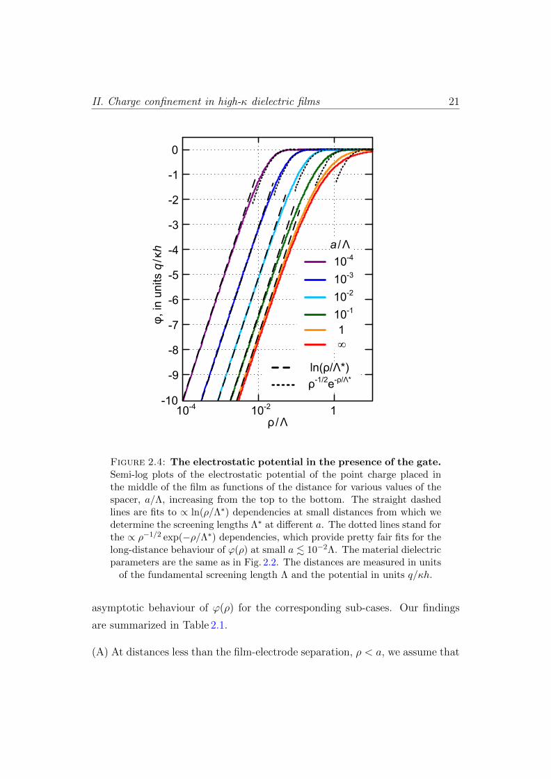
Shown in Fig. 2.4 is the semi-log plot of the potential versus the distance calcu-
lated for the same parameters as in Fig. 2.2. We clearly observe the change of
behaviour from the logarithmic one to the fast decay at longer distances. The
corresponding screening length at which the crossover occurs, Λ∗, is evaluated
via the abscissa section by the straight line corresponding to ϕ(ρ) ∝ ln(ρ/Λ∗)
at small ρ.
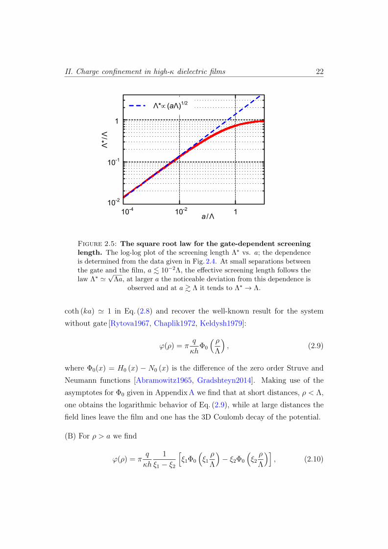
Plotting the dependance of Λ∗ on a in a double-log scale (Fig. 2.5), we find
Λ∗ ∝√a at a . 10−1Λ. At larger a, the Λ∗(a) dependence starts to deviate
from the square root behaviour, and, eventually, at sufficiently large a the
influence of the gate vanishes and Λ∗ saturates to Λ. Inspecting more carefully
the transition region around a ∼ 10−1Λ, one observes that the functional
dependence of the screened potential changes its character. At these scales
the potential is pretty well described as ϕ(ρ) ∝ exp(−ρ/Λ∗) with the same
Λ∗ ∝√a (see Fig. 2.4) at a . 10−1Λ. At a & 10−1Λ the potential decays as a
power ϕ(ρ) ∝ ρ−n, with n . 3.
2.2.3 A zoo of interaction regimes
To gain insight into the observed behaviours of the potential, we undertake the
detailed analysis of two asymptotic cases, ρ > a and ρ < a, in which the exact
formulae for ϕ(ρ) can be obtained. Considering possible relations between a
and other relevant spatial scales, we derive, with the logarithmic accuracy, the
II. Charge confinement in high-κ dielectric films 21
-10
-9
-8
-7
-6
-5
-4
-3
-2
-1
0
a /Λ
10-4
10-3
10-2
10-1
1
ln(ρ/Λ*)
ρ-1/2e-ρ/Λ*
ρ /Λ
φ, i
n un
its q
/κh
10-4 10-2 1
Figure 2.4: The electrostatic potential in the presence of the gate.Semi-log plots of the electrostatic potential of the point charge placed inthe middle of the film as functions of the distance for various values of thespacer, a/Λ, increasing from the top to the bottom. The straight dashedlines are fits to ∝ ln(ρ/Λ∗) dependencies at small distances from which wedetermine the screening lengths Λ∗ at different a. The dotted lines stand forthe ∝ ρ−1/2 exp(−ρ/Λ∗) dependencies, which provide pretty fair fits for thelong-distance behaviour of ϕ(ρ) at small a . 10−2Λ. The material dielectricparameters are the same as in Fig. 2.2. The distances are measured in units
of the fundamental screening length Λ and the potential in units q/κh.
asymptotic behaviour of ϕ(ρ) for the corresponding sub-cases. Our findings
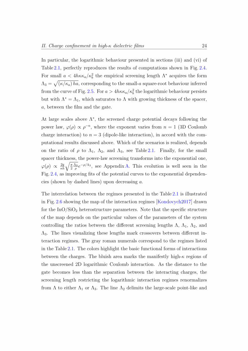
are summarized in Table 2.1.
(A) At distances less than the film-electrode separation, ρ < a, we assume that
II. Charge confinement in high-κ dielectric films 22
Λ* (aΛ)1/2
a /Λ
Λ*/
Λ
10-4 10-2 110-2
10-1
1
Figure 2.5: The square root law for the gate-dependent screeninglength. The log-log plot of the screening length Λ∗ vs. a; the dependenceis determined from the data given in Fig. 2.4. At small separations betweenthe gate and the film, a . 10−2Λ, the effective screening length follows thelaw Λ∗ '
√Λa, at larger a the noticeable deviation from this dependence is
observed and at a & Λ it tends to Λ∗ → Λ.
coth (ka) ' 1 in Eq. (2.8) and recover the well-known result for the system
without gate [Rytova1967, Chaplik1972, Keldysh1979]:
ϕ(ρ) = πq
κhΦ0
( ρΛ
), (2.9)
where Φ0(x) = H0 (x) − N0 (x) is the difference of the zero order Struve and
Neumann functions [Abramowitz1965, Gradshteyn2014]. Making use of the
asymptotes for Φ0 given in Appendix A we find that at short distances, ρ < Λ,
one obtains the logarithmic behavior of Eq. (2.9), while at large distances the
field lines leave the film and one has the 3D Coulomb decay of the potential.
(B) For ρ > a we find
ϕ(ρ) = πq
κh
1
ξ1 − ξ2
[ξ1Φ0
(ξ1ρ
Λ
)− ξ2Φ0
(ξ2ρ
Λ
)], (2.10)
II. Charge confinement in high-κ dielectric films 23
ρ < a
(i)
ρ < Λ
ϕ(ρ) ' −2 qκh
ln Cρ2Λ
(ii)
ρ > Λ
ϕ(ρ) ' 2 q(κa+κb)ρ
ρ > a
a > 4hκκaκ2b
(iii)
ρ < Λ1 < Λ2
ϕ ' −2 qκh
ln Cρ2Λ1
(iv)
Λ1 < ρ < Λ2
ϕ ' 2(κ2b−4κaκh/a)1/2
qρ
(v)
Λ1 < Λ2 < ρ
ϕ ' 2 κbκ2a
qa2
ρ3
a < 4hκκaκ2b
(vi)
ρ < Λ3
ϕ ' −2 qκh
ln Cρ2Λ3
(vii)
ρ > Λ3
ϕ ' 2 κbκ2a
qa2
ρ3
Table 2.1: Regimes of the interaction. There are two major regions,short distances, ρ < a, where interaction is only weakly influenced by thegate (upper panel), and large distances, ρ > a, where the gate presencerenormalizes the interaction (bottom panel). Logarithmic dependence on ρappears below the respective screening lengths, Λ, Λ1 and Λ3. Above theselengths the potential decays according to the power law. The constant
C = eγ ' 1.781... is the exponent of the Euler constant γ.
where
ξ1,2 =1
2(κa + κb)
[κb ±
√κ2b − 4κaκh/a
].
Depending on a, the length-scaling parameters, ξ1 and ξ2 can be either the
real numbers, if a > 4hκκa/κ2b , or the complex mutually conjugated numbers,
if a < 4hκκa/κ2b . This leads to the different regimes of the potential decay
(see Table 1) that are controlled by the new screening lengths, Λ1,2 = Λ/ξ1,2
(Λ1 < Λ2) in the former case and Λ3 = Λ/ |ξ1| = Λ/ |ξ2| in the latter one.
II. Charge confinement in high-κ dielectric films 24
In particular, the logarithmic behaviour presented in sections (iii) and (vi) of
Table 2.1, perfectly reproduces the results of computations shown in Fig. 2.4.
For small a < 4hκκa/κ2b the empirical screening length Λ∗ acquires the form
Λ3 =√
(κ/κa)ha, corresponding to the small-a square-root behaviour inferred
from the curve of Fig. 2.5. For a > 4hκκa/κ2b the logarithmic behaviour persists
but with Λ∗ = Λ1, which saturates to Λ with growing thickness of the spacer,
a, between the film and the gate.
At large scales above Λ∗, the screened charge potential decays following the
power law, ϕ(ρ) ∝ ρ−n, where the exponent varies from n = 1 (3D Coulomb
charge interaction) to n = 3 (dipole-like interaction), in accord with the com-
putational results discussed above. Which of the scenarios is realized, depends
on the ratio of ρ to Λ1, Λ2, and Λ3, see Table 2.1. Finally, for the small
spacer thickness, the power-law screening transforms into the exponential one,
ϕ(ρ) ∝ 2qκh
√π2
Λ3
ρe−ρ/Λ3 , see Appendix A. This evolution is well seen in the
Fig. 2.4, as improving fits of the potential curves to the exponential dependen-
cies (shown by dashed lines) upon decreasing a.
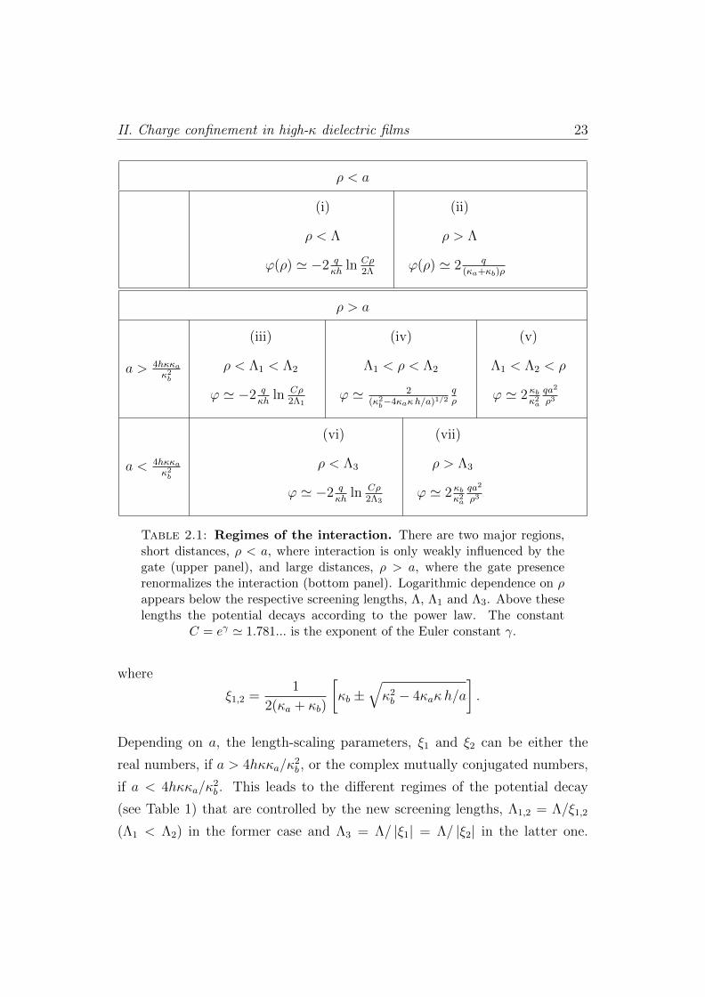
The interrelation between the regimes presented in the Table 2.1 is illustrated
in Fig. 2.6 showing the map of the interaction regimes [Kondovych2017] drawn
for the InO/SiO2 heterostructure parameters. Note that the specific structure
of the map depends on the particular values of the parameters of the system
controlling the ratios between the different screening lengths Λ, Λ1, Λ2, and
Λ3. The lines visualizing these lengths mark crossovers between different in-
teraction regimes. The gray roman numerals correspond to the regimes listed
in the Table 2.1. The colors highlight the basic functional forms of interactions
between the charges. The bluish area marks the manifestly high-κ regions of
the unscreened 2D logarithmic Coulomb interaction. As the distance to the
gate becomes less than the separation between the interacting charges, the
screening length restricting the logarithmic interaction regimes renormalizes
from Λ to either Λ1 or Λ3. The line Λ2 delimits the large-scale point-like and
II. Charge confinement in high-κ dielectric films 25
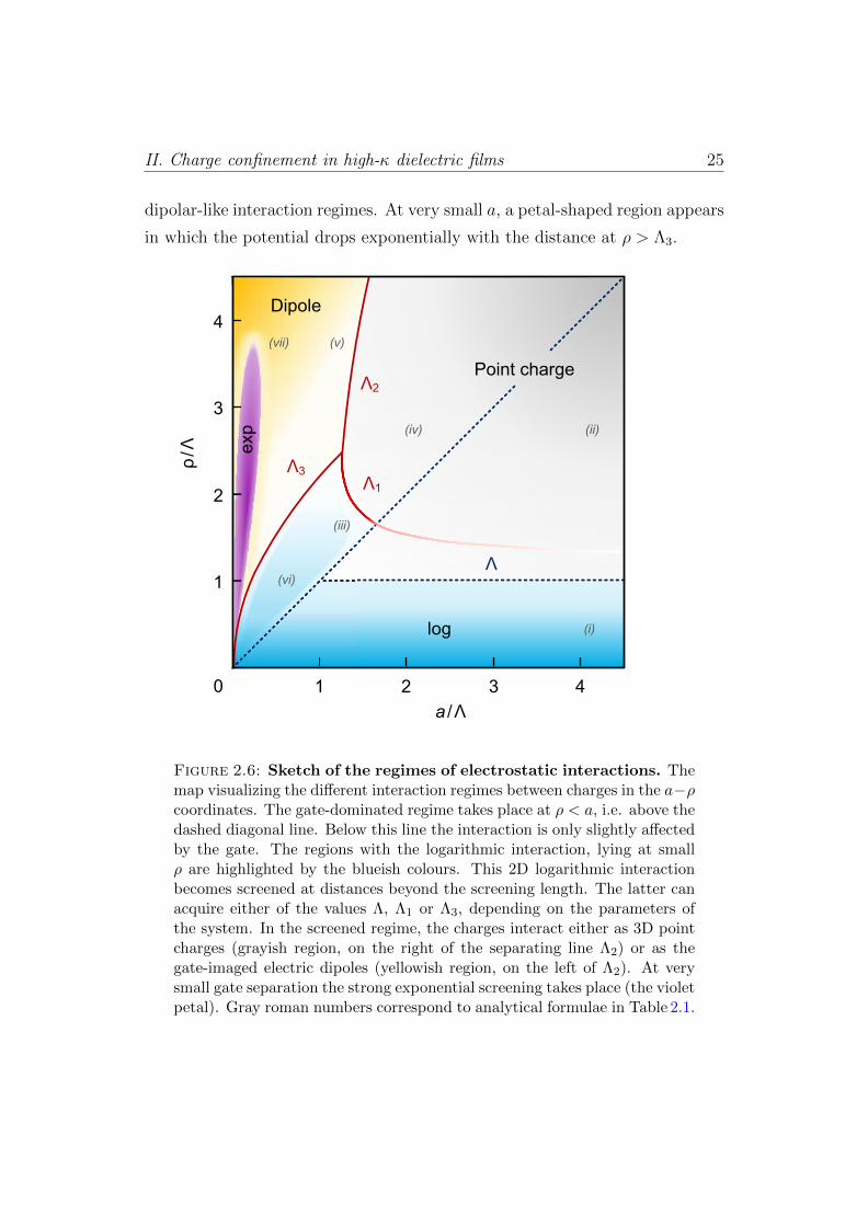
dipolar-like interaction regimes. At very small a, a petal-shaped region appears
in which the potential drops exponentially with the distance at ρ > Λ3.
1 2 3 4
a /Λ
log
Dipole
Point charge
exp
Λ2
Λ3
1
2
3
4
ρ/Λ
0
Λ
(i)
(ii)(iv)
(v)(vii)
(vi)
(iii)
Λ1
Figure 2.6: Sketch of the regimes of electrostatic interactions. Themap visualizing the different interaction regimes between charges in the a−ρcoordinates. The gate-dominated regime takes place at ρ < a, i.e. above thedashed diagonal line. Below this line the interaction is only slightly affectedby the gate. The regions with the logarithmic interaction, lying at smallρ are highlighted by the blueish colours. This 2D logarithmic interactionbecomes screened at distances beyond the screening length. The latter canacquire either of the values Λ, Λ1 or Λ3, depending on the parameters ofthe system. In the screened regime, the charges interact either as 3D pointcharges (grayish region, on the right of the separating line Λ2) or as thegate-imaged electric dipoles (yellowish region, on the left of Λ2). At verysmall gate separation the strong exponential screening takes place (the violetpetal). Gray roman numbers correspond to analytical formulae in Table 2.1.
II. Charge confinement in high-κ dielectric films 26
2.3 Discussion and experimental outlook
The achieved results, summarized in Table 2.1 as well as conveniently sketched
in Fig. 2.6, describe a wealth of electrostatic regimes in which the high-κ sheets
can operate depending on the distance to the control gate.
The implications of the tunability of the electrostatic interaction type are far
reaching. The possibility to drive the electrostatic properties of the high-κ 2D
systems generates the technological advantages for their use as nanoscale ca-
pacitor components, novel memory elements and switching devices of enhanced
performance. The profound application of the high-κ sheets is the fabrication
of the charge-trapping memory (CTM) units [Zhao2014], enabling the storage
of the multiple bits in a single memory cell, thus overcoming the scalability
limit of a standard flash memory. The challenging task crucial to the device
realization is establishing the effective tunability of CTM units allowing for
controlling the strength and spatial scale of charge distribution. Based on the
results hereinabove, one possible solution is to introduce the controlled gate
in the system and govern the charge density in the film by changing the dis-
tance to the gate thus adjusting the length of the electrostatic screening. The
reduction of the Coulomb repulsion from the 2D long-range logarithmic to the
point- or dipolar- and even to the exponential ones will crucially scale down
the memory element size, increasing the capacity and reliability of the high-κ
films-based flash memory circuits.
A striking manifestation of the 2D logarithmic Coulomb behaviour is the
phenomenon of superinsulation in strongly disordered superconducting films
[Vinokur2008, Baturina2013, Baturina2008, Kalok2012]. There, in the critical
vicinity of the superconductor-insulator transition, the superconducting film
acquires an anomalously high dielectric constant κ, the Cooper pairs inter-
act according to the logarithmic law, and the system experiences the charge
Berezinskii-Kosterlitz-Thouless (BKT) transition into a state with the infinite
resistance. The general consequence of the logarithmic Coulomb interaction, is
II. Charge confinement in high-κ dielectric films 27
that the high-κ sheets exhibit the so-called phenomenon of the global Coulomb
blockade resulting in a logarithmic scaling of characteristic energies of the sys-
tem with the relevant screening length, which is the smallest of either Λ or the
lateral system size. In the CTM element discussed before, this is the logarith-
mic scaling of its capacitance. In the Cooper pair insulator, this comes out as
the logarithmic scaling of the energy controlling the in-plane tunneling con-
ductivity [Fistul2008, Vinokur2008, Baturina2011], thus being the foundation
of the charge BKT transition. Adjusting the gate spacer, one can can regulate
the effects of diverging dielectric constant near the metal- and superconductor-
insulator transitions [Baturina2013]. Tuning the range of the charge confine-
ment offers a perfect laboratory for the study of effects of screening on the
BKT transition and related phenomena.
Bibliography
[Abramowitz1965] Abramowitz, M. & Stegun, I. Handbook of Mathematical
Functions (Dover Publications, 1965).
[Baturina2008] Baturina, T. I., Mironov, A. Y., Vinokur, V., Baklanov, M. &
Strunk, C. Hyperactivated resistance in TiN films on the insulating side of
the disorder-driven superconductor-insulator transition. JETP Lett. 88,
752–757 (2008).
[Baturina2011] Baturina, T. I. et al. Nanopattern-stimulated superconductor-
insulator transition in thin TiN films. EPL (Europhys. Lett.) 93, 47002
(2011).
[Baturina2013] Baturina, T. I. & Vinokur, V. M. Superinsulator–supercon-
ductor duality in two dimensions. Annals of Physics 331, 236–257 (2013).
[Castner1975] Castner, T. G., Lee, N. K., Cieloszyk, G. S. & Salinger, G. L.
Dielectric anomaly and the metal-insulator transition in n-type silicon.
Phys. Rev. Lett. 34, 1627–1630 (1975).
[Chaplik1972] Chaplik, A. & Entin, M. Charged impurities in very thin layers.
Sov. Phys. JETP 34, 1335–1339 (1972).
[Fistul2008] Fistul, M., Vinokur, V. & Baturina, T. Collective Cooper-pair
transport in the insulating state of Josephson-junction arrays. Phys. Rev.
Lett. 100, 086805 (2008).
28
II. Charge confinement in high-κ dielectric films 29
[Gradshteyn2014] Gradshteyn, I. S. & Ryzhik, I. M. Table of integrals, series,
and products (Academic press, 2014).
[Grannan1981] Grannan, D. M., Garland, J. C. & Tanner, D. B. Critical
behavior of the dielectric constant of a random composite near the perco-
lation threshold. Phys. Rev. Lett. 46, 375–378 (1981).
[Hess1982] Hess, H. F., DeConde, K., Rosenbaum, T. F. & Thomas, G. A. Gi-
ant dielectric constants at the approach to the insulator-metal transition.
Phys. Rev. B 25, 5578–5580 (1982).
[Kalok2012] Kalok, D. et al. Non-linear conduction in the critical region of
the superconductor-insulator transition in TiN thin films. J. Phys.: Conf.
Ser. 400, 022042 (2012).
[Keldysh1979] Keldysh, L. Coulomb interaction in thin semiconductor and
semimetal films. JETP Lett. 29, 658–661 (1979).
[Kondovych2017] Kondovych, S., Luk’yanchuk, I., Baturina, T. I. & Vinokur,
V. M. Gate-tunable electron interaction in high-κ dielectric films. Sci.
Rep. 7, 42770 (2017).
[Osada2012] Osada, M. & Sasaki, T. Two-dimensional dielectric nanosheets:
Novel nanoelectronics from nanocrystal building blocks. Advanced Mate-
rials 24, 210–228 (2012).
[Rytova1967] Rytova, N. Screened potential of a point charge in the thin film.
Vestnik MSU (in Russian) 3, 30–37 (1967).
[Vinokur2008] Vinokur, V. M. et al. Superinsulator and quantum synchro-
nization. Nature 452, 613–615 (2008).
[Watanabe2000] Watanabe, M., Itoh, K. M., Ootuka, Y. & Haller, E. E. Local-
ization length and impurity dielectric susceptibility in the critical regime
of the metal-insulator transition in homogeneously doped p-type Ge. Phys.
Rev. B 62, R2255–R2258 (2000).
II. Charge confinement in high-κ dielectric films 30
[Yakimov1997] Yakimov, A. & Dvurechenskii, A. Metal-insulator transition
in amorphous Si1−cMnc obtained by ion implantation. JETP Lett. 65,
354–358 (1997).
[Zhao2014] Zhao, C., Zhao, C. Z., Taylor, S. & Chalker, P. R. Review on
non-volatile memory with high-k dielectrics: flash for generation beyond
32 nm. Materials 7, 5117–5145 (2014).
Chapter 3
Extended linear charges in
dielectric films
Charge carrying elements are usual parts of novel nanodevices, thus requiring
the careful investigation of their physical properties and their impact on the
other parts of the device and on the overall functionality of the system. To
describe properly the electrostatic interactions between the extended charges
in materials, we utilize the methods and results discussed in Chapters 1 and
2, generalizing the calculations from zero-dimensional to one-dimensional sys-
tems, namely linear charges. The next two Chapters are devoted to the deriva-
tion of the electrostatic potential distribution created by linear charged objects,
– such as charged wires, stripes, and charged domain walls, – inside dielectric
and ferroelectric materials.
Once the electrostatics of a charged wire is known, one example of the possible
application could be the use of two interacting wires as a capacitor, allowing the
determination of the material dielectric constant via capacitance measurement.
The details of the corresponding analytical modeling constitute the essence of
this Chapter.
31
III. Extended linear charges in dielectric films 32
3.1 Capacitance measurement methods in thin
dielectric films
Miniaturization of electronic devices down to the nano-scale has become pos-
sible by achieving the unprecedentedly efficient material functionalities not
available in bulk systems. A large variety of novel nanoscale materials ex-
tends from thin films and superlattices [Shi2003, Lakhtakia2005, Ramesh2007,
Zhang2010, Hass2013], nanowires [Zhang2016], to nanoparticles and particle
composites (see e.g. [Chatzigeorgiou2015] and references therein), the unique
properties of which open a way to various implementations for nanoelectron-
ics. In particular, tailoring the properties of substrate-deposited thin films by
strain has attracted particular attention due to technological feasibility and
various potential applications such as sensors, actuators, nonvolatile memo-
ries, bio-membranes, photovoltaic cells, tunable microwave circuits and micro-
and nano- electromechanical systems [Shi2003, Lakhtakia2005, Ramesh2007,
Zhang2010, Hass2013]. Control and measurement of the dielectric constant ε of
thin films present one of the major objectives of strain-engineering technology
to achieve the optimal dielectric properties of constructed nanodevices.
The arising difficulty, however, is that the conventional technique for measure-
ment of ε, consisting in the determination of capacitance of a two-electrode
plate capacitor, C = ε0εS/h (where ε0 is the vacuum permittivity, S is the elec-
trode surface and h is the distance between plates), is not suitable here. The
bottom-electrode deposition at the film-substrate interface, if ever possible,
perturbs the functionality and integrity of the device, whereas the top-electrode
can influence the optical characterization of the system. In addition, defect-
provided leakage currents across thin film can distort the results. The emer-
gent technique of nanoscale capacitance microscopy [Shao2003, Gomila2008]
that measures the capacitance between an atomic force microscope tip and the
film is also limited by the same requirement of film deposition on a conductive
substrate.
III. Extended linear charges in dielectric films 33
A non-destructive way to overcome these difficulties consists in employing a
capacitor in which both electrodes are located outside but in close proximity
to the film. The capacitance of the system will depend on its geometry and
in particular on the dielectric constants of film and substrate that finally per-
mits to measure ε. However, determination of such functional dependence is
the complicated electrostatic problem that, in general, requires cumbersome
numerical calculations. The semi-analytical method of capacitance calculation
for a particular case of planar capacitor in which two semi-infinite electrode
plates with parallel, linearly aligned edges are deposited on the top of the film
was proposed by Vendik et al. [Vendik1999]. This geometry attracted the
experimental audience due to the simplicity and intuitive clarity of the result-
ing formula. Under the reasonable experimental conditions, the capacitance
of the planar capacitor was found to be inversely proportional to the width
of the edge-separated gap transmission line, d, and can be approximated as
C = ε0εS/d where S is the cross-sectional area of the film below the elec-
trode edge. This expression is formally equivalent to the capacitance of a
parallel-plate capacitor of thickness d, in which the electrodes correspond to
the cross-sectional regions.
Note, however, that Vendik’s method is limited to the case when the dielectric
constant of the film (we set it as ε2) is much bigger than the dielectric constants
of the environment media, ε1, and the substrate, ε3, and when the transmis-
sion gap is thinner than the film thickness [Deleniv1999]. This restriction is
related to the used “partial capacitance” or “magnetic wall” approximations
in which the film, the substrate and the environment space are assumed to be
electrostatically independent of each other and the electric field lines do not
emerge from the deposited film. Being justified for the upper subspace, which
is normally air with ε1 = 1, the partial capacitance approximation can be not
accurate enough if the dielectric constant of the substrate is bigger than (or
comparable to) that of the film.
III. Extended linear charges in dielectric films 34
The objective of the present work is to propose the procedure for non-destructive
measurements of the dielectric constant of the films, valid for any types of the
substrate and environment media. We consider the geometry in which two par-
allel wire electrodes are placed on top of the film and derive the exact formula
for the capacitance of such system. Our calculations don’t imply the partial
capacitance approximation and therefore are valid for nanofilm-substrate de-
vices based on the vast class of materials, extending from semiconductors to
oxide multiferroics.
3.2 Electrostatics of a charged wire in a dielec-
tric thin film
The geometry of the system is shown in Fig. 3.1. Two parallel wires with
opposite linear charge densities, ±ql, are located on top of the ferroelectric
film. The distance between the wires, d, is much larger than their radius, R,
and the film thickness, h. We also account for anisotropy of the film, assuming
that the in-plane (transverse) dielectric constant differs from the out-of-plane
(longitudinal) one, ε2, by the anisotropy factor η2 and is equal to η2ε2. The
origin of the rectangular coordinate system is selected in the middle of the
film, just below the left wire. The z-axis is directed perpendicular to the film
plane, the y-axis is directed along the wires and the x-axis is perpendicular to
them. Thus, left and right wires have the coordinates (0, y, h/2) and (d, y, h/2)
correspondingly. The translational symmetry of this system in y-direction
permits to reduce the consideration to the 2D space, (x, z).
Using the methods of electrostatics we calculate the distribution of the elec-
trostatic potential induced by one of the wires (left one in Fig. 3.1). The
corresponding Poisson equations have to be written separately for each con-
stituent part of the system – the external environment space (region 1), film
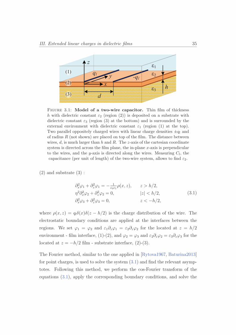
III. Extended linear charges in dielectric films 35
Figure 3.1: Model of a two-wire capacitor. Thin film of thicknessh with dielectric constant ε2 (region (2)) is deposited on a substrate withdielectric constant ε3 (region (3) at the bottom) and is surrounded by theexternal environment with dielectric constant ε1 (region (1) at the top).Two parallel oppositely charged wires with linear charge densities ±ql andof radius R (not shown) are placed on top of the film. The distance betweenwires, d, is much larger than h and R. The z-axis of the cartesian coordinatesystem is directed across the film plane, the in-plane x-axis is perpendicularto the wires, and the y-axis is directed along the wires. Measuring Cl, thecapacitance (per unit of length) of the two-wire system, allows to find ε2.
(2) and substrate (3) :
∂2xϕ1 + ∂2
zϕ1 = − 1ε0ε1
ρ(x, z), z > h/2,
η2∂2xϕ2 + ∂2
zϕ2 = 0, |z| < h/2,
∂2xϕ3 + ∂2
zϕ3 = 0, z < −h/2,
(3.1)
where ρ(x, z) = qlδ(x)δ(z − h/2) is the charge distribution of the wire. The
electrostatic boundary conditions are applied at the interfaces between the
regions. We set ϕ1 = ϕ2 and ε1∂zϕ1 = ε2∂zϕ2 for the located at z = h/2
environment - film interface, (1)-(2), and ϕ2 = ϕ3 and ε2∂zϕ2 = ε3∂zϕ3 for the
located at z = −h/2 film - substrate interface, (2)-(3).
The Fourier method, similar to the one applied in [Rytova1967, Baturina2013]
for point charges, is used to solve the system (3.1) and find the relevant asymp-
totes. Following this method, we perform the cos-Fourier transform of the
equations (3.1), apply the corresponding boundary conditions, and solve the
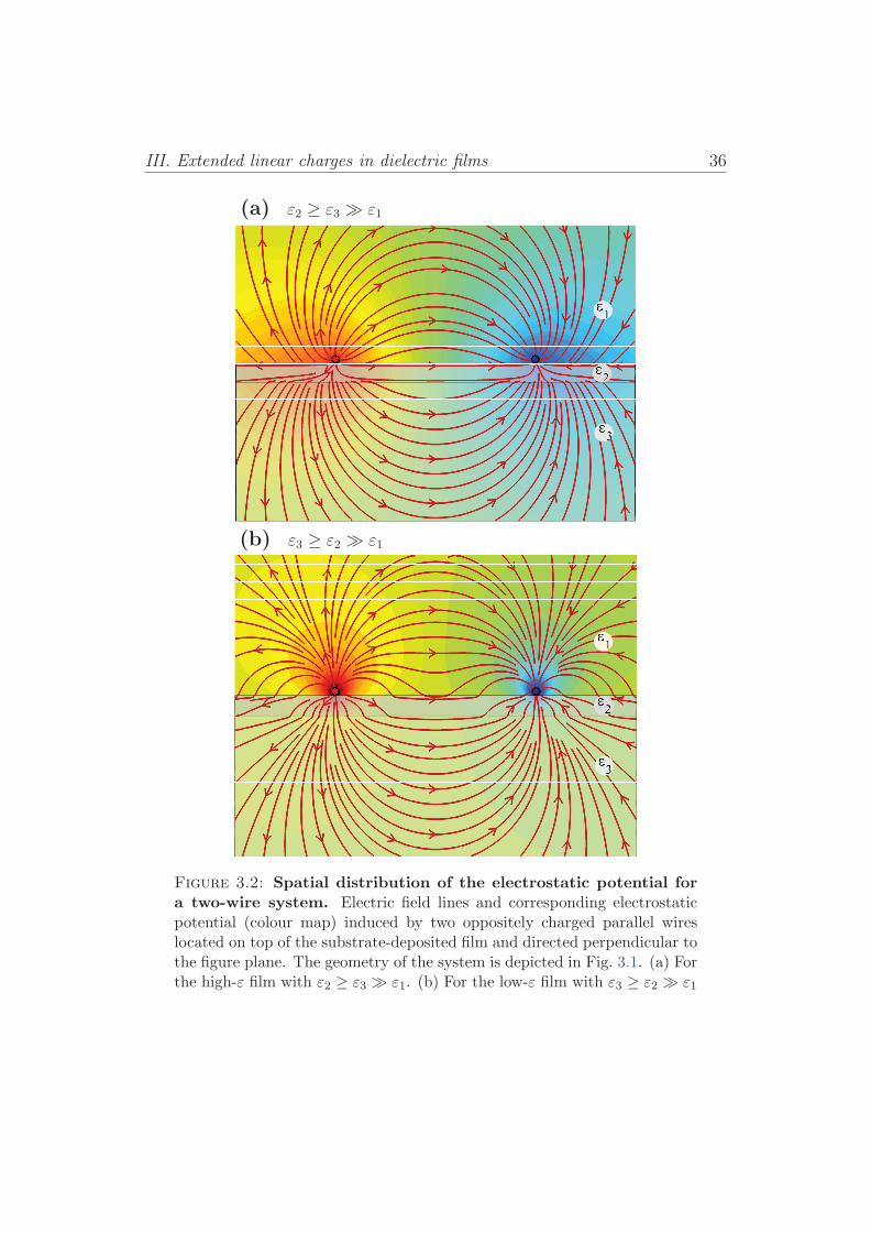
III. Extended linear charges in dielectric films 36
(a) ε2 ≥ ε3 ε1
(b) ε3 ≥ ε2 ε1
Figure 3.2: Spatial distribution of the electrostatic potential fora two-wire system. Electric field lines and corresponding electrostaticpotential (colour map) induced by two oppositely charged parallel wireslocated on top of the substrate-deposited film and directed perpendicular tothe figure plane. The geometry of the system is depicted in Fig. 3.1. (a) Forthe high-ε film with ε2 ≥ ε3 ε1. (b) For the low-ε film with ε3 ≥ ε2 ε1
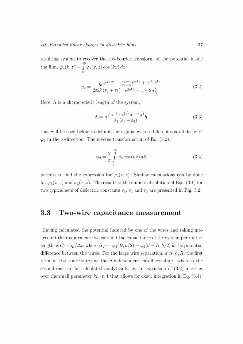
III. Extended linear charges in dielectric films 37
resulting system to recover the cos-Fourier transform of the potential inside
the film, ϕ2(k, z) =∞∫0
ϕ2(x, z) cos (kx) dx:
ϕ2 =qle
ηkh/2
2ε0k (ε2 + ε1)
ε2−ε3ε2+ε3
e−kz + eηkhekz
e2ηkh − 1 + 2η hΛ
. (3.2)
Here, Λ is a characteristic length of the system,
Λ = η(ε2 + ε1) (ε2 + ε3)
ε2 (ε1 + ε3)h, (3.3)
that will be used below to delimit the regions with a different spatial decay of
ϕ2 in the x-direction. The inverse transformation of Eq. (3.2),
ϕ2 =2
π
∞∫0
ϕ2 cos (kx) dk, (3.4)
permits to find the expression for ϕ2(x, z). Similar calculations can be done
for ϕ1(x, z) and ϕ3(x, z). The results of the numerical solution of Eqs. (3.1) for
two typical sets of dielectric constants ε1, ε2 and ε3 are presented in Fig. 3.2.
3.3 Two-wire capacitance measurement
Having calculated the potential induced by one of the wires and taking into
account their equivalence we can find the capacitance of the system per unit of
length as Cl = ql/∆ϕ where ∆ϕ = ϕ2(R, h/2)− ϕ2(d−R, h/2) is the potential
difference between the wires. For the large wire separation, d h,R, the first
term in ∆ϕ contributes as the d-independent cutoff constant, whereas the
second one can be calculated analytically, by an expansion of (3.2) in series
over the small parameter kh 1 that allows for exact integration in Eq. (3.4).
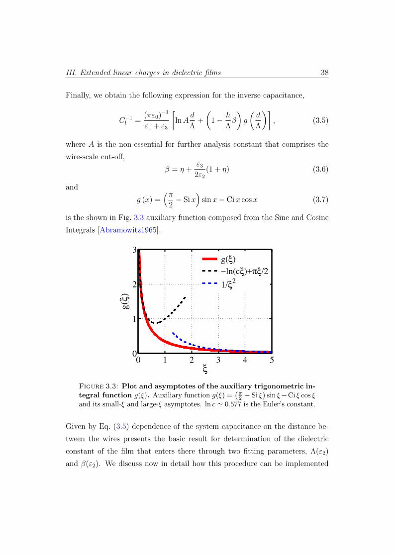
III. Extended linear charges in dielectric films 38
Finally, we obtain the following expression for the inverse capacitance,
C−1l =
(πε0)−1
ε1 + ε3
[lnA
d
Λ+
(1− h
Λβ
)g
(d
Λ
)], (3.5)
where A is the non-essential for further analysis constant that comprises the
wire-scale cut-off,
β = η +ε3
2ε2
(1 + η) (3.6)
and
g (x) =(π
2− Six
)sinx− Cix cosx (3.7)
is the shown in Fig. 3.3 auxiliary function composed from the Sine and Cosine
Integrals [Abramowitz1965].
ξ
g(ξ
)
0 1 2 3 4 50
1
2
3 g(ξ)
−ln(cξ)+πξ/2
1/ξ2
Figure 3.3: Plot and asymptotes of the auxiliary trigonometric in-tegral function g(ξ). Auxiliary function g(ξ) =
(π2 − Si ξ
)sin ξ−Ci ξ cos ξ
and its small-ξ and large-ξ asymptotes. ln c ' 0.577 is the Euler’s constant.
Given by Eq. (3.5) dependence of the system capacitance on the distance be-
tween the wires presents the basic result for determination of the dielectric
constant of the film that enters there through two fitting parameters, Λ(ε2)
and β(ε2). We discuss now in detail how this procedure can be implemented
III. Extended linear charges in dielectric films 39
in practice, considering for simplicity the isotropic film with η = 1, encom-
passed by the external environment with ε1 ε2, ε3 that gives β = 1 + ε3/ε2
and Λ = (1 + ε2/ε3)h. We analyze separately the cases of high-ε and low-
ε films (with ε2 ≥ ε3 ε1 and ε3 ≥ ε2 ε1 correspondingly) that have
different electrostatic behavior. As shown in Fig. 3.2, wires-induced electric
field lines are “repelled” from the film in the first case (Fig. 3.2,a) and “cap-
tured” by the film in the second one (Fig. 3.2,b). Fig. 3.4 presents given
by Eq. (3.2) dependence of the inverse capacitance C−1l , measured in units
(πε0ε3)−1 = 3.6 × 10⁴ε−13 µm/pF, on the relative distance between the wires,
d/h, for both cases.
3.3.1 High-ε film, ε2 ≥ ε3 ε1
For a large ratio ε2/ε3 the characteristic scale λ can be comparable and even
larger than the linear size of the system, and therefore the g-function can be
expanded over the small parameter d/Λ as g (d/Λ) ' − ln (cd/Λ) + πd/2Λ
[Abramowitz1965], (Fig. 3.3), where ln c is the Euler’s constant, ln cn→∞=
Σnk=1 k
−1− lnn ' 0.577. Then, the resulting expression for C−1l can be simpli-
fied to:
C−1l = const +
1
ε0ε2
d
2h, (3.8)
that permits to measure ε2 via the linear slope of dependence C−1l (d) at d→ 0
(Fig. 3.4,a). This method is analogous to that for geometry of planar capacitor
with semi-infinite plates [Vendik1999] due to the similar linear dependence on
the distance between electrodes. Presented in Fig. 3.4,a numerical analysis
shows, however, some restrictions for the application of this method. The
distance between electrodes at which the linearity is manifested should be
rather small (but still larger than R and h) and the parameter ε2/ε3 should be
large enough.
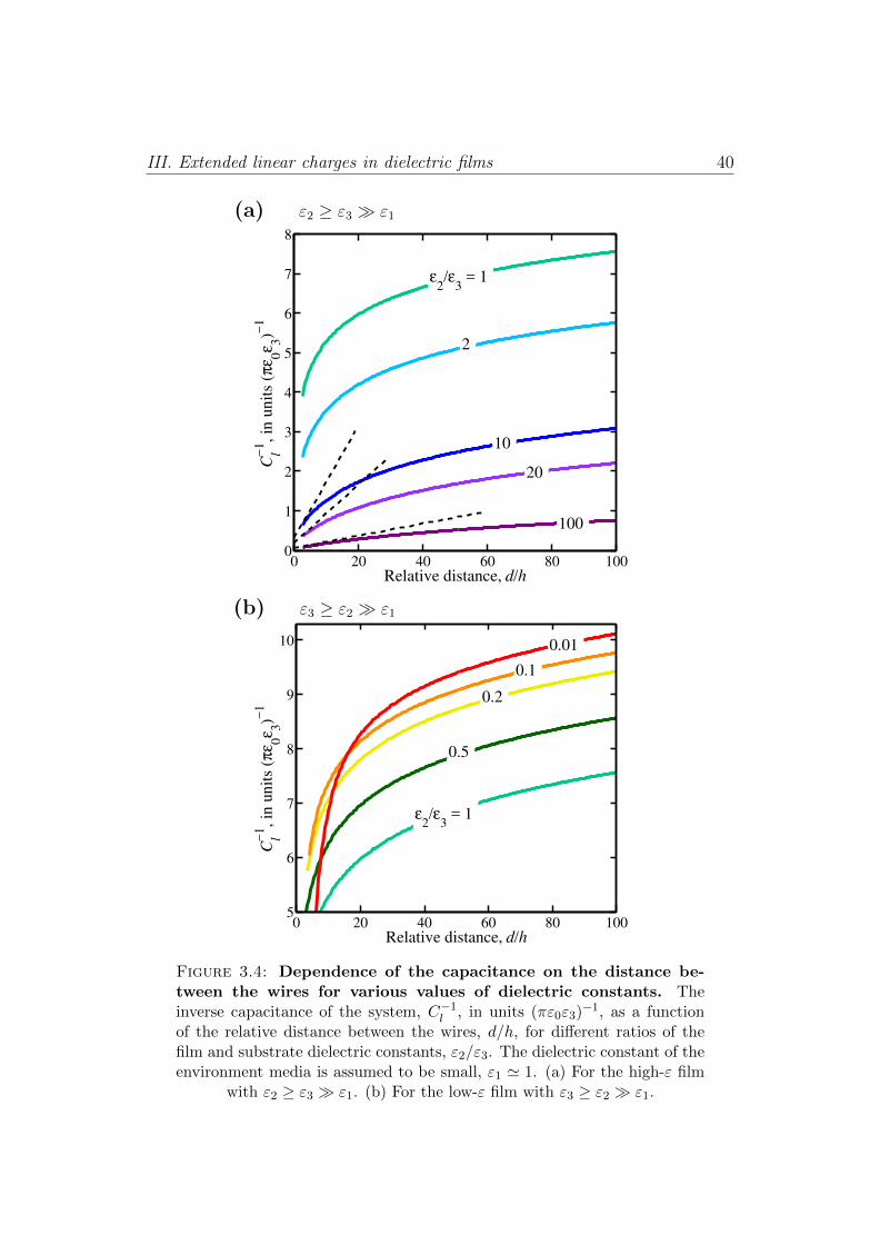
III. Extended linear charges in dielectric films 40
(a) ε2 ≥ ε3 ε1
100
20
10
2
ε2/ε
3 = 1
Relative distance, d/h
Cl−
1,
in u
nit
s (π
ε0ε
3)−
1
0 20 40 60 80 1000
1
2
3
4
5
6
7
8
(b) ε3 ≥ ε2 ε1
ε2/ε
3 = 1
0.5
0.2
0.1
0.01
Relative distance, d/h
Cl−
1, in
unit
s (π
ε0ε
3)−
1
0 20 40 60 80 1005
6
7
8
9
10
Figure 3.4: Dependence of the capacitance on the distance be-tween the wires for various values of dielectric constants. Theinverse capacitance of the system, C−1
l , in units (πε0ε3)−1, as a functionof the relative distance between the wires, d/h, for different ratios of thefilm and substrate dielectric constants, ε2/ε3. The dielectric constant of theenvironment media is assumed to be small, ε1 ' 1. (a) For the high-ε film
with ε2 ≥ ε3 ε1. (b) For the low-ε film with ε3 ≥ ε2 ε1.
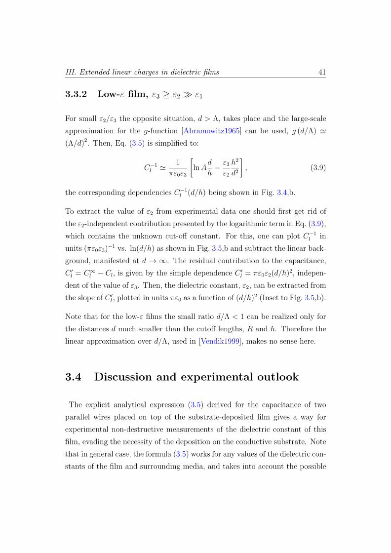
III. Extended linear charges in dielectric films 41
3.3.2 Low-ε film, ε3 ≥ ε2 ε1
For small ε2/ε3 the opposite situation, d > Λ, takes place and the large-scale
approximation for the g-function [Abramowitz1965] can be used, g (d/Λ) '(Λ/d)2. Then, Eq. (3.5) is simplified to:
C−1l '
1
πε0ε3
[lnA
d
h− ε3
ε2
h2
d2
], (3.9)
the corresponding dependencies C−1l (d/h) being shown in Fig. 3.4,b.
To extract the value of ε2 from experimental data one should first get rid of
the ε2-independent contribution presented by the logarithmic term in Eq. (3.9),
which contains the unknown cut-off constant. For this, one can plot C−1l in
units (πε0ε3)−1 vs. ln(d/h) as shown in Fig. 3.5,b and subtract the linear back-
ground, manifested at d → ∞. The residual contribution to the capacitance,
C ′l = C∞l − Cl, is given by the simple dependence C ′l = πε0ε2(d/h)2, indepen-
dent of the value of ε3. Then, the dielectric constant, ε2, can be extracted from
the slope of C ′l , plotted in units πε0 as a function of (d/h)2 (Inset to Fig. 3.5,b).
Note that for the low-ε films the small ratio d/Λ < 1 can be realized only for
the distances d much smaller than the cutoff lengths, R and h. Therefore the
linear approximation over d/Λ, used in [Vendik1999], makes no sense here.
3.4 Discussion and experimental outlook
The explicit analytical expression (3.5) derived for the capacitance of two
parallel wires placed on top of the substrate-deposited film gives a way for
experimental non-destructive measurements of the dielectric constant of this
film, evading the necessity of the deposition on the conductive substrate. Note
that in general case, the formula (3.5) works for any values of the dielectric con-
stants of the film and surrounding media, and takes into account the possible
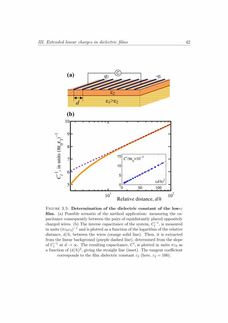
III. Extended linear charges in dielectric films 42
ql
d
-ql
ε3>ε2
ε2
C(a)
(b)
101
102
5
6
7
8
9
10
Relative distance, d/h
Cl−
1,
in u
nit
s (π
ε0ε
3)−
1
0 50 1000
5
10
15
(d/h)2
C′/πε0×10
−3
Figure 3.5: Determination of the dielectric constant of the low-εfilm. (a) Possible scenario of the method application: measuring the ca-pacitance consequently between the pairs of equidistantly placed oppositelycharged wires. (b) The inverse capacitance of the system, C−1
l , is measuredin units (πε0ε3)−1 and is plotted as a function of the logarithm of the relativedistance, d/h, between the wires (orange solid line). Then, it is extractedfrom the linear background (purple dashed line), determined from the slopeof C−1
l at d→∞. The resulting capacitance, C ′, is plotted in units πε0 asa function of (d/h)2, giving the straight line (inset). The tangent coefficient
corresponds to the film dielectric constant ε2 (here, ε2 = 100).
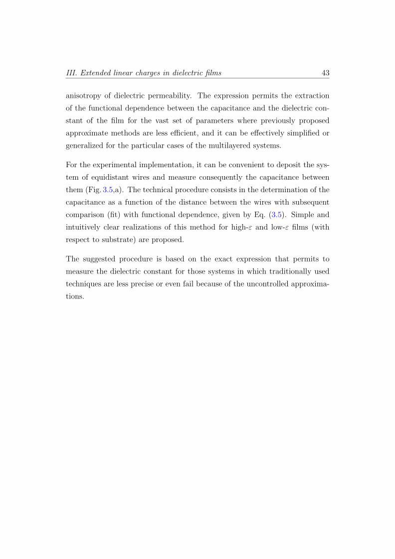
III. Extended linear charges in dielectric films 43
anisotropy of dielectric permeability. The expression permits the extraction
of the functional dependence between the capacitance and the dielectric con-
stant of the film for the vast set of parameters where previously proposed
approximate methods are less efficient, and it can be effectively simplified or
generalized for the particular cases of the multilayered systems.
For the experimental implementation, it can be convenient to deposit the sys-
tem of equidistant wires and measure consequently the capacitance between
them (Fig. 3.5,a). The technical procedure consists in the determination of the
capacitance as a function of the distance between the wires with subsequent
comparison (fit) with functional dependence, given by Eq. (3.5). Simple and
intuitively clear realizations of this method for high-ε and low-ε films (with
respect to substrate) are proposed.
The suggested procedure is based on the exact expression that permits to
measure the dielectric constant for those systems in which traditionally used
techniques are less precise or even fail because of the uncontrolled approxima-
tions.
Bibliography
[Abramowitz1965] Abramowitz, M. & Stegun, I. Handbook of Mathematical
Functions (Dover Publications, 1965).
[Baturina2013] Baturina, T. I. & Vinokur, V. M. Superinsulator–supercon-
ductor duality in two dimensions. Annals of Physics 331, 236–257 (2013).
[Chatzigeorgiou2015] Chatzigeorgiou, G., Javili, A. & Steinmann, P. Inter-
face properties influence the effective dielectric constant of composites.
Philosophical Magazine 95, 3402–3412 (2015).
[Deleniv1999] Deleniv, A. N. On the question of the error in the partial ca-
pacitance method. Tech. Phys. 44, 356–360 (1999).
[Gomila2008] Gomila, G., Toset, J. & Fumagalli, L. Nanoscale capacitance
microscopy of thin dielectric films. J. Appl. Phys. 104, 024315 (2008).
[Hass2013] Hass, G., Francombe, M. H. & Hoffman, R. W. Physics of Thin
Films: Advances in Research and Development (Elsevier, 2013).
[Kondovych2017] Kondovych, S. & Luk’yanchuk, I. Nondestructive method of
thin-film dielectric constant measurements by two-wire capacitor. Phys.
Status Solidi B 254, 1600476 (2017).
[Lakhtakia2005] Lakhtakia, A. & Messier, R. Sculptured thin films: nanoengi-
neered morphology and optics (SPIE press Bellingham, WA, 2005).
44
III. Extended linear charges in dielectric films 45
[Ramesh2007] Ramesh, R. & Spaldin, N. A. Multiferroics: progress and
prospects in thin films. Nature materials 6, 21–29 (2007).
[Rytova1967] Rytova, N. S. Screened potential of a point charge in the thin
film. Vestnik MSU (in Russian) 3, 30–37 (1967).
[Shao2003] Shao, R., Kalinin, S. V. & Bonnell, D. A. Local impedance imag-
ing and spectroscopy of polycrystalline ZnO using contact atomic force
microscopy. Appl. Phys. Lett. 82, 1869–1871 (2003).
[Shi2003] Shi, D. Functional thin films and functional materials: new concepts
and technologies (Springer Science & Business Media, 2003).
[Vendik1999] Vendik, O. G., Zubko, S. P. & Nikolskii, M. A. Modeling and cal-
culation of the capacitance of a planar capacitor containing a ferroelectric
thin film. Tech. Phys. 44, 349–355 (1999).
[Zhang2016] Zhang, A. Zheng, G. & Leiber, C. Nanowires: Building Blocks
for Nanoscience and Nanotechnology (Springer International Publishing,
2016).
[Zhang2010] Zhang, S. Nanostructured thin films and coatings: mechanical
properties (CRC Press, 2010).
Chapter 4
In-plane domains and domain
walls in ferroic films
Nano-sized particles, wires and thin films, which are the common parts of
modern nanoelectronic devices, possess a number of peculiar physical prop-
erties compared with bulk materials, due to significant increase of the sur-
face/interface impact [Dawber2005, Scott2007]. In ferroic materials at meso-
and nanoscale, the finite-size, shape and surface effects highly influence the
equilibrium state of the sample, including the domain structure formation.
High sensitivity of domain-patterned thin ferroic films to external fields allows
to drive and control their functionalities for implementation into up-to-date
technologies, e.g. information storage devices, terahertz emitters and detec-
tors, nanoantennas etc. Ferromagnetic (FM), ferroelectric (FE) and multifer-
roic films often perform as field-tuned parts of multilayered heterostructures,
and thus domain distribution in one layer can affect the state of the other layer,
or domain dynamics in the ferroic layer may change the dynamic properties of
the whole structure. Great variety of domain structure types and their depen-
dance on many parameters (crystal anisotropy, temperature, sample geometry,
46
IV. In-plane domains and domain walls in ferroic films 47
mechanical stress, external fields applied etc.) make domain-textured mate-
rials attractive not only for industrial applications, but also for fundamental
studies in material physics.
Stripe-like 180 domain structure in thin FM, and, in recent years, FE films
and multilayers with out-of-plane uniaxial anisotropy is being intensively stud-
ied, showing a wealth of unique properties. The periodic out-of plain domain
texture was observed in thin films and superlattices, [Streiffer2002, Zubko2010,
Zubko2012, Hruszkewycz2013], and its behaviour is in agreement with theoreti-
cal models [Bratkovsky2000, Kornev2004, Stephanovich2005, Luk’yanchuk2009,
Sene2010, Mokry2004, Aguado-Puente2008] As the most striking example of
the discovered phenomena we may cite the recently theoretically predicted
[Luk’yanchuk2014a] and experimentally confirmed [Zubko2016] existence of
the negative capacitance in thin ferroelectric domain-patterned layer.
For the striped out-of-plane domain structures in FM and FE thin films, the
equilibrium domain width d depends on film’s thikhness h as d ∼√h, as it
was predicted for ferromagnets by Landau and Lifshitz [Landau1935] and Kittel
[Kittel1946, Kittel1949]. Though this square-root law is suitable in many cases,
and was approved and specified for particular systems, it should be stressed
that for thin FM and FE films with in-plane magnetization/polarization easy
axis, the relation between the domain period and sample size can differ. In
this Chapter, we use the methods of electrostatics to perform the analytical
calculation and capture this difference in the domain distribution law between
the out-of-plane and in-plane orientations of the order parameter in ferroic
materials.
Note that we consider two ways of the in-plane domain structure forma-
tion. The first is based on the finite sample size, and domains appear due
to the existence of the discontinuity of the order parameter at the sample
edge. Such finite-size-induced in-plane domain formation was discussed for
the FM (see, e.g. [Kashuba1993, Gulyaev2002]) and antiferromagnetic (AFM)
IV. In-plane domains and domain walls in ferroic films 48
[Folven2010, Gomonay2014] flat nanoparticles. The modeling of the in-plane
magnetic domain structure is performed in the first Section of this Chapter.
The second possible way to induce the striped domain structure appearance is
to create a domain wall inside a sample by the external means. For example,
generating a charged domain wall (CDW) in the FE slab with the electri-
cally biased microscope tip [Lu2015] caused the formation of head-to-head (or
tail-to-tail, depending on the charge of the CDW) stripe domains, which are
modelled in the second Section. The analysis of a particular case of the tip-
induced polarization switching and hence creation of a single in-plane domain
completes the Chapter.
4.1 Periodic Kittel domain structure in thin
ferroic films with in-plane anisotropy
4.1.1 In-plane 180 stripe domains: geometry and model
Consider a thin film (thickness h, linear size l h) with the uniaxial in-
plane anisotropy (electric or magnetic) of the order parameter P , which in the
case of the ferroelectric material denotes the electric polarization P, and can
be replaced by the magnetization vector M for magnetic systems with ε =
1. Analogously to the conventional problem with out-of-plane geometry, we
argue that the discontinuity of the order parameter at the film’s edge produces
magnetic field, which enhances energy of the system. In order to diminish the
total energy, the striped in-plane periodic domain structure occurs in the film
(Fig. 4.1,a), with the period 2d. In this Chapter we work within the Kittel
approximation [Kittel1949], assuming the temperatures much lower than the
transition temperature.
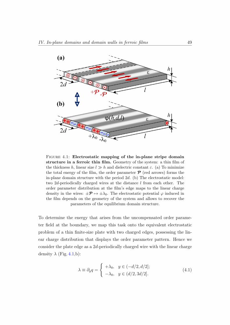
IV. In-plane domains and domain walls in ferroic films 49
Figure 4.1: Electrostatic mapping of the in-plane stripe domainstructure in a ferroic thin film. Geometry of the system: a thin film ofthe thickness h, linear size l h and dielectric constant ε. (a) To minimizethe total energy of the film, the order parameter P (red arrows) forms thein-plane domain structure with the period 2d. (b) The electrostatic model:two 2d-periodically charged wires at the distance l from each other. Theorder parameter distribution at the film’s edge maps to the linear chargedensity in the wires: ±P 7→ ±λ0. The electrostatic potential ϕ induced inthe film depends on the geometry of the system and allows to recover the
parameters of the equilibrium domain structure.
To determine the energy that arises from the uncompensated order parame-
ter field at the boundary, we map this task onto the equivalent electrostatic
problem of a thin finite-size plate with two charged edges, possessing the lin-
ear charge distribution that displays the order parameter pattern. Hence we
consider the plate edge as a 2d-periodically charged wire with the linear charge
density λ (Fig. 4.1,b):
λ ≡ ∂yq =
+λ0, y ∈ (−d/2, d/2];
−λ0, y ∈ (d/2, 3d/2].(4.1)
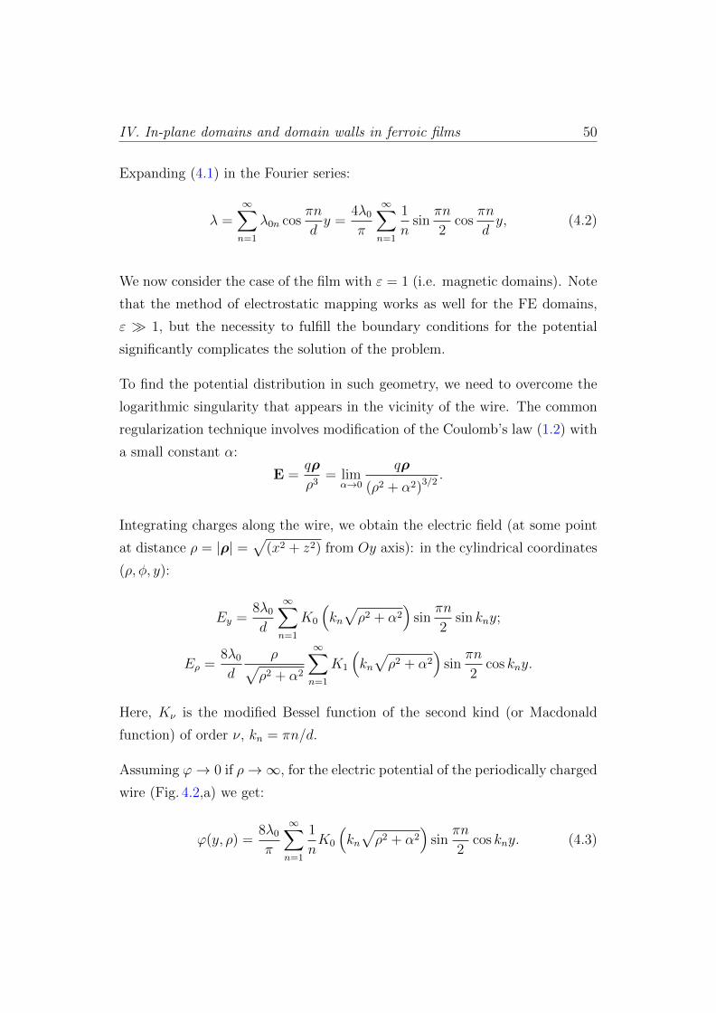
IV. In-plane domains and domain walls in ferroic films 50
Expanding (4.1) in the Fourier series:
λ =∞∑n=1
λ0n cosπn
dy =
4λ0
π
∞∑n=1
1
nsin
πn
2cos
πn
dy, (4.2)
We now consider the case of the film with ε = 1 (i.e. magnetic domains). Note
that the method of electrostatic mapping works as well for the FE domains,
ε 1, but the necessity to fulfill the boundary conditions for the potential
significantly complicates the solution of the problem.
To find the potential distribution in such geometry, we need to overcome the
logarithmic singularity that appears in the vicinity of the wire. The common
regularization technique involves modification of the Coulomb’s law (1.2) with
a small constant α:
E =qρ
ρ3= lim
α→0
qρ
(ρ2 + α2)3/2.
Integrating charges along the wire, we obtain the electric field (at some point
at distance ρ = |ρ| =√
(x2 + z2) from Oy axis): in the cylindrical coordinates
(ρ, φ, y):
Ey =8λ0
d
∞∑n=1
K0
(kn√ρ2 + α2
)sin
πn
2sin kny;
Eρ =8λ0
d
ρ√ρ2 + α2
∞∑n=1
K1
(kn√ρ2 + α2
)sin
πn
2cos kny.
Here, Kν is the modified Bessel function of the second kind (or Macdonald
function) of order ν, kn = πn/d.
Assuming ϕ→ 0 if ρ→∞, for the electric potential of the periodically charged
wire (Fig. 4.2,a) we get:
ϕ(y, ρ) =8λ0
π
∞∑n=1
1
nK0
(kn√ρ2 + α2
)sin
πn
2cos kny. (4.3)
IV. In-plane domains and domain walls in ferroic films 51
z
yx
dh
yx
z
d
(a) (b)
++ ++
++
++ ++
++
Figure 4.2: Periodically charged linear systems. The simplest modelfor the periodically charged edge: (a) charged wire or (b) charged stripe withthe linear charge density being the rectangular function ±λ0 with period 2d.y-axis of the Cartesian coordinate system is directed along the wire (stripe);
the stripe thickness h defines the direction of z-axis.
4.1.2 General expression for the electrostatic energy of
the periodically charged stripe
The result 4.3 for the charged wire is helpful for the problem in Fig. 4.1, when
the film is very thin, h l, so that we are allowed to neglect the size of
the charged edge. However, it is interesting to generalize the problem for the
thicker films and study the influence of the edge size on the final result. So,
the objective is to find the electrostatic potential distribution created by the
periodically charged stripe of width h shown in Fig. 4.2,b.
One way to obtain the sought-for potential (denoted as φ) is to integrate the
already found expression for the charged wire (4.3) along the stripe width h,
φ =
∫dϕ(y, ρ) = (4.4)
=8λ0
πh
∞∑n=1
1
nsin
πn
2cos (kny)
h/2∫−h/2
K0
(kn
√x2 + (z − z′)2 + α2
)dz′,
Denoting the integral in the expression above as S,
IV. In-plane domains and domain walls in ferroic films 52
S (x, z) =
h/2∫−h/2
K0
(kn
√x2 + (z − z′)2 + α2
)dz′,
we may find the energy per unit of length along the charged plate, averaged
on period, in the form (for derivation, see Appendix B, part B.1):
Fel =1
2
∫φdq =
8λ20
π2h2
∞∑n=1
1
n2sin2 πn
2
h/2∫−h/2
S (x = 0, z) dz. (4.5)
Taking into account the the regularization constant α is small compared to sys-
tem size, the integral in (4.5) can be estimated as (see Appendix B, part B.2):
h/2∫−h/2
S (x = 0, z) dz ≈ −h2
[2
k2nh
2+
1
2knhG(k2nh
2
4
)]. (4.6)
Here, G denotes a particular case of Meijer G-function [Abramowitz1965]:
G(k2nh
2
4
)≡ G2,1
1,3
(1;−−1
2, 1
2; 0
∣∣∣∣∣ k2nh
2
4
), (4.7)
which has the following asymptotics (Fig. 4.3):
ξ → 0 : G2,11,3
(1;−−1
2, 1
2; 0
∣∣∣∣∣ ξ2
)∼ −2
ξ− 6ξ + 4ξ ln cξ;
ξ →∞ : G2,11,3
(1;−−1
2, 1
2; 0
∣∣∣∣∣ ξ2
)→ −2π. (4.8)
With this estimation, the electrostatic energy per unit of stripe length (4.5)
acquires the form:
Fel = −4λ20
π2
∞∑n=1
1
n2sin2 πn
2
[4
k2nh
2+
1
knhG(k2nh
2
4
)]. (4.9)
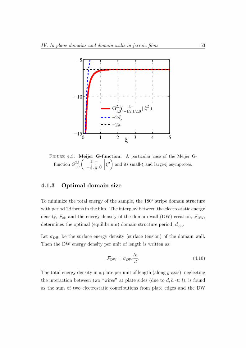
IV. In-plane domains and domain walls in ferroic films 53
ξ
0 1 2 3 4 5−15
−10
−5
G1,3
2,1(
1;−
−1/2,1/2;0 | ξ
2 )
−2/ξ
−2π
Figure 4.3: Meijer G-function. A particular case of the Meijer G-
function G2,11,3
(1;−−1
2 ,12 ; 0
∣∣∣∣ ξ2
)and its small-ξ and large-ξ asymptotes.
4.1.3 Optimal domain size
To minimize the total energy of the sample, the 180 stripe domain structure
with period 2d forms in the film. The interplay between the electrostatic energy
density, Fel, and the energy density of the domain wall (DW) creation, FDW,
determines the optimal (equilibrium) domain structure period, dopt.
Let σDW be the surface energy density (surface tension) of the domain wall.
Then the DW energy density per unit of length is written as:
FDW = σDWlh
d. (4.10)
The total energy density in a plate per unit of length (along y-axis), neglecting
the interaction between two “wires” at plate sides (due to d, h l), is found
as the sum of two electrostatic contributions from plate edges and the DW
IV. In-plane domains and domain walls in ferroic films 54
energy density:
Ftotal = 2Fel + FDW. (4.11)
Minimization of the total energy (4.11) with respect to the domain structure
half-period d allows to obtain the expression for the optimal domain width dopt
(for derivation see Appendix B, part B.3):
d2opt
∞∑n=1
1
n3f
(πnh
dopt
)sin2 πn
2=π3h2σDW
32λ20
l, (4.12)
where we use the notation
f
(πnh
d
)= f (knh) = K1 (knh)− 2
knh− 1
4G(k2nh
2
4
).
Next, we consider two limit cases, in which the expression (4.12) simplifies:
1) very thick charged edge; and 2) narrow, wire-like charged edge.
4.1.3.1 Wide charged edge: transition to the Kittel’s problem
In the case of the large stripe width, h l, the task converts to a well-
known problem of the out-of-plane stripe domain structure. It is easy to show,
limiting the film thickness in the expression (4.12) to infinity, h → ∞, then
K1 is exponentially small and f(πnhd
)→ π/2 hence:
d2opt
∞∑n=1
1
n3sin2 πn
2=π2h2σDW
16λ20
l. (4.13)
Note that for the case of an infinitely large plate, h→∞, the integral in (4.5)
is known (see Appendix B, part B.2), and leads to the same expression. Next,
taking into account that
∞∑n=1
1
n3sin2 πn
2=
∞∑m=0
1
(2m+ 1)3=
7
8ζ(3),
IV. In-plane domains and domain walls in ferroic films 55
ζ(3) ≈ 1.202 is a Riemann zeta function, and DW surface tension for 180
domain walls can be estimated using the order parameter P as σDW ∼ P2∆
[Landau1984], with ∆ being a DW thickness, ∆ d. Also, the performed
electrostatic mapping (Fig. 4.1) implies λ0 ∼ Ph, and hence
d2opt =
8
7ζ(3)
π2h2σDW16λ2
0
l ' π2∆
14ζ(3)l, (4.14)
we obtain the famous Kittel’s square root law [Kittel1946, Kittel1949]:
dopt '
√π2
14ζ(3)
√l∆ = 0.77
√l∆. (4.15)
4.1.3.2 Narrow charged edge: in-plane domains in thin film
The second limit case of the expression (4.12) turns us back to the main
objective of this Chapter: study of in-plane 180 domain structure in thin
films. When h l, d, then using (4.8) and the series representation K1(ξ) '1ξ
+ ξ2
ln cξ2− ξ
4, we get f
(πnhd
)' πnh
2dand the expression (4.12) simplifies to:
dopt
∞∑n=1
1
n2sin2 πn
2=π2hσDW
16λ20
l. (4.16)
The sum in (4.16) gives another Riemann zeta function,
∞∑n=1
1
n2sin2 πn
2=
∞∑m=0
1
(2m+ 1)2=
3
4ζ(2),
ζ(2) = π2
6. Substituting everything to the expression gives:
dopt '∆
2
l
h. (4.17)
IV. In-plane domains and domain walls in ferroic films 56
Note that this result can be also directly obtained using the expression (4.3)
for the charged wire potential. Similar calculations were performed and dis-
cussed in [Gulyaev2002] for the in-plane ferromagnetic domain structure. The
electrostatic energy density per unit of wire length can be written as:
Fel =1
2
∫ϕdq =
1
2
1
2d
2d∫0
(ϕλ)ρ=0 dy =8λ2
0
π2
∞∑m=0
1
(2m+ 1)2K0
(π (2m+ 1)
dα
).
Recalling that α is a small regularization parameter, we may expand the Mac-
donald function in series K0 (ξ) ' − ln cξ2
, and get
Fel ' −8λ2
0
π2
[lncπα
2d
∞∑m=0
1
(2m+ 1)2 +∞∑m=0
ln (2m+ 1)
(2m+ 1)2
].
here, c ≈ 1.781 is the exponential of the Euler constant. Using the relations
[Prudnikov1986]:
∞∑k=0
1
(2k + 1)2 =3
4ζ(2),
∞∑k=0
ln (2k + 1)
(2k + 1)2 = −1
4ζ (2) ln 2− 3
4ζ ′ (2) ,
and ζ(2) = π2/6, we finally obtain:
Fel = λ20 ln
Ad
α,
where A ≡ 2 3√2cπ
exp(
6π2 ζ′ (2)
)unites all the numerical constants. Note that
the singularity is hidden in the term −λ20 lnα, which limits to the infinity if
α→ 0, but this term does not depend on the system’s geometry and thus will
not affect the equilibrium domain structure.
The total energy density of the film can thus be written as:
F = 2Fel + FDW = 2λ20 ln
Ad
α+ σDW
lh
d,
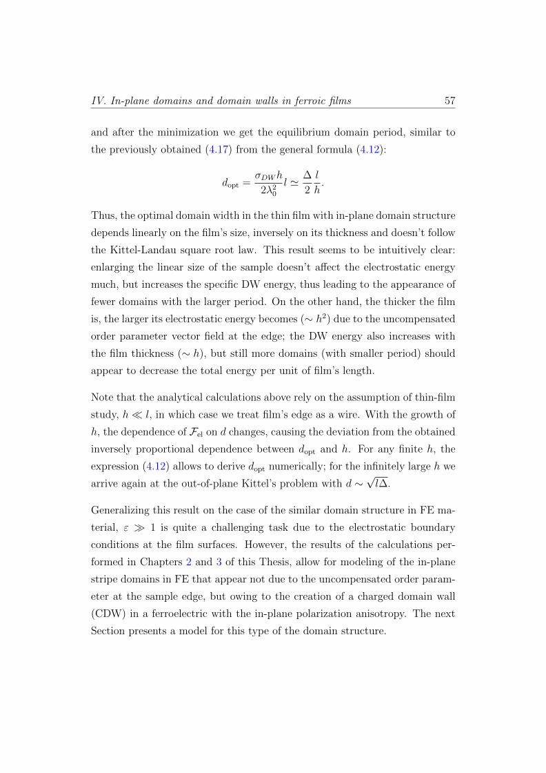
IV. In-plane domains and domain walls in ferroic films 57
and after the minimization we get the equilibrium domain period, similar to
the previously obtained (4.17) from the general formula (4.12):
dopt =σDWh
2λ20
l ' ∆
2
l
h.
Thus, the optimal domain width in the thin film with in-plane domain structure
depends linearly on the film’s size, inversely on its thickness and doesn’t follow
the Kittel-Landau square root law. This result seems to be intuitively clear:
enlarging the linear size of the sample doesn’t affect the electrostatic energy
much, but increases the specific DW energy, thus leading to the appearance of
fewer domains with the larger period. On the other hand, the thicker the film
is, the larger its electrostatic energy becomes (∼ h2) due to the uncompensated
order parameter vector field at the edge; the DW energy also increases with
the film thickness (∼ h), but still more domains (with smaller period) should
appear to decrease the total energy per unit of film’s length.
Note that the analytical calculations above rely on the assumption of thin-film
study, h l, in which case we treat film’s edge as a wire. With the growth of
h, the dependence of Fel on d changes, causing the deviation from the obtained
inversely proportional dependence between dopt and h. For any finite h, the
expression (4.12) allows to derive dopt numerically; for the infinitely large h we
arrive again at the out-of-plane Kittel’s problem with d ∼√l∆.
Generalizing this result on the case of the similar domain structure in FE ma-
terial, ε 1 is quite a challenging task due to the electrostatic boundary
conditions at the film surfaces. However, the results of the calculations per-
formed in Chapters 2 and 3 of this Thesis, allow for modeling of the in-plane
stripe domains in FE that appear not due to the uncompensated order param-
eter at the sample edge, but owing to the creation of a charged domain wall
(CDW) in a ferroelectric with the in-plane polarization anisotropy. The next
Section presents a model for this type of the domain structure.
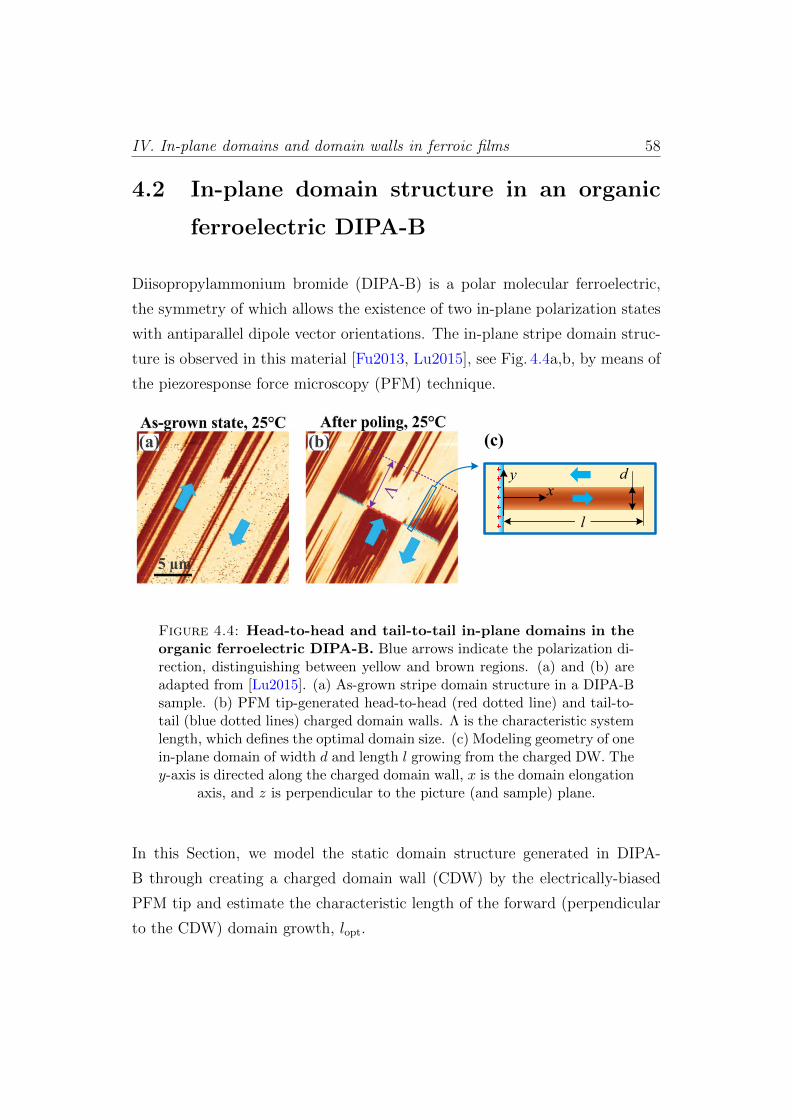
IV. In-plane domains and domain walls in ferroic films 58
4.2 In-plane domain structure in an organic
ferroelectric DIPA-B
Diisopropylammonium bromide (DIPA-B) is a polar molecular ferroelectric,
the symmetry of which allows the existence of two in-plane polarization states
with antiparallel dipole vector orientations. The in-plane stripe domain struc-
ture is observed in this material [Fu2013, Lu2015], see Fig. 4.4a,b, by means of
the piezoresponse force microscopy (PFM) technique.
(c)
l
dx
y
Figure 4.4: Head-to-head and tail-to-tail in-plane domains in theorganic ferroelectric DIPA-B. Blue arrows indicate the polarization di-rection, distinguishing between yellow and brown regions. (a) and (b) areadapted from [Lu2015]. (a) As-grown stripe domain structure in a DIPA-Bsample. (b) PFM tip-generated head-to-head (red dotted line) and tail-to-tail (blue dotted lines) charged domain walls. Λ is the characteristic systemlength, which defines the optimal domain size. (c) Modeling geometry of onein-plane domain of width d and length l growing from the charged DW. They-axis is directed along the charged domain wall, x is the domain elongation
axis, and z is perpendicular to the picture (and sample) plane.
In this Section, we model the static domain structure generated in DIPA-
B through creating a charged domain wall (CDW) by the electrically-biased
PFM tip and estimate the characteristic length of the forward (perpendicular
to the CDW) domain growth, lopt.
IV. In-plane domains and domain walls in ferroic films 59
4.2.1 Model of the striped domains in DIPA-B
To model the formation of the domain structure in DIPA-B microcrystals, let
us consider a sample of the thickness h and dielectric tensor main components
(ε2x, ε2y, ε2z) deposited on the substrate with the dielectric constant ε3 and
surrounded by medium with the dielectric constant ε1 (usually air with ε1 = 1).
In the experimental work [Lu2015] the substrate is Pt-coated Si, thus there is
a conducting layer under the FE slab, which we will take into account later.
Assume that there is a tip-induced CDW along (0, y, [−h/2 h/2]) with the
surface charge density qs. Fig. 4.4c shows the sample from above: the z-axis
of the Cartesian coordinate system is perpendicular to the picture plane, thus
the sample thickness h is not shown. The y-axis goes along the CDW, while
the x-axis is perpendicular to it. The domains grow from the CDW along the
x-axis; one of them is shown schematically in the Figure, having the width d
and length l.
The model of such a system resembles the one described in Chapter 3, however,
there are several nuances we need to take into account. First, we consider
having a wide (almost the thickness of the film h) CDW tail-to-tail (or head-to-
head) instead of the near-surface charged “wire” (with the coordinates (0, y, a)
and the linear charge density ql), as it was in the previous Chapter. The
second difference is due to the properties of the material: DIPA-B is a uniaxial
ferroelectric with the in-plane polar axis in the slab (x-axis in Fig. 4.4c), so
ε2y = ε2z 6= ε2x, and we need to include the dielectric constant anisotropy
factor η2 = ε2x/ε2z. The equations (3.1) for the electrostatic potential ϕ1,2,3
(above the slab, in the slab, and in the substrate, respectively) then transform
into:
∂2xϕ1 + ∂2
zϕ1 = 0, z > h/2,
ε2x∂2xϕ2 + ε2z∂
2zϕ2 = − qs
ε0δ(x), |z| < h/2,
∂2xϕ3 + ∂2
zϕ3 = 0, z < −h/2,(4.18)
IV. In-plane domains and domain walls in ferroic films 60
δ(x) is the Dirac delta-function. The boundary conditions are: ϕ1 = ϕ2 and
ε1∂zϕ1 = ε2z∂zϕ2 at z = h/2; ϕ2 = ϕ3 and ε2z∂zϕ2 = ε3∂zϕ3 at z = −h/2.
Using the Fourier method and applying the BCs, we reconstruct the expression
for the cos-Fourier transform of the electrostatic potential ϕ2 at the surface of
the film (z = h/2) induced by a charged stripe, at distances larger than the
film thickness (x h):
ϕ2 'qsh
2ε0 (ε1 + ε3)
1
k (kΛ + 1).
Here, the characteristic length (3.3) with the anisotropic factor appears:
Λ = η(ε2z + ε1) (ε2z + ε3)
ε2z (ε1 + ε3)h. (4.19)
The inverse cos-Fourier transform leads to the answer for the potential,
ϕ2 = − qsh
πε0(ε1 + ε3)
[ln(cx
Λ
)+ g
(xΛ
)],
where ln c is the Euler’s constant, ln cn→∞= Σn
k=1 k−1 − lnn ' 0.577; and the
g-function, defined as g (t) =(π2− Si t
)sin t− Ci t cos t, is one of the auxiliary
trigonometric integral functions, see Fig. 3.3.
Note that for the discussed case of the ferroelectric plate deposited on the
conducting substrate, we may apply the method of images and solve for the
“mirrored” in the conducting layer system instead; then, h 7→ 2h, ε3 = ε1. The
parameters for the DIPA-B system from [Lu2015]: ε2z ≈ 40, ε2x ≈ 80, ε1 = 1,
thus ε2x,z ε1, then the characteristic length, Λ, simplifies to: Λ = ηε2zh =√ε2xε2zh, and the resulting expression for the potential:
ϕ2 = − qshπε0
[ln
(c
x√ε2xε2zh
)+ g
(x
√ε2xε2zh
)].
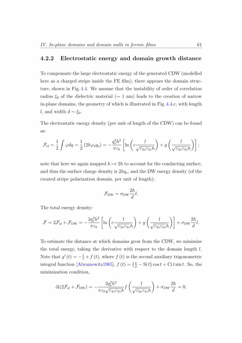
IV. In-plane domains and domain walls in ferroic films 61
4.2.2 Electrostatic energy and domain growth distance
To compensate the large electrostatic energy of the generated CDW (modelled
here as a charged stripe inside the FE film), there appears the domain struc-
ture, shown in Fig. 4.4. We assume that the instability of order of correlation
radius ξ0 of the dielectric material (∼ 1 nm) leads to the creation of narrow
in-plane domains, the geometry of which is illustrated in Fig. 4.4,c, with length
l, and width d ∼ ξ0.
The electrostatic energy density (per unit of length of the CDW) can be found
as:
Fel =1
2
∫ϕdq =
1
2(2hϕ2qs) = −q
2sh
2
πε0
[ln
(c
l√ε2xε2zh
)+ g
(l
√ε2xε2zh
)];
note that here we again mapped h 7→ 2h to account for the conducting surface,
and thus the surface charge density is 2hqs, and the DW energy density (of the
created stripe polarization domain, per unit of length):
FDW = σDW2h
dl.
The total energy density:
F = 2Fel + FDW = −2q2sh
2
πε0
[ln
(c
l√ε2xε2zh
)+ g
(l
√ε2xε2zh
)]+ σDW
2h
dl.
To estimate the distance at which domains grow from the CDW, we minimize
the total energy, taking the derivative with respect to the domain length l.
Note that g′ (t) = −1t
+ f (t), where f (t) is the second auxiliary trigonometric
integral function [Abramowitz1965], f (t) =(π2− Si t
)cos t+ Ci t sin t. So, the
minimization condition,
∂l(2Fel + FDW) = − 2q2sh
2
πε0√ε2xε2zh
f
(l
√ε2xε2zh
)+ σDW
2h
d= 0,
IV. In-plane domains and domain walls in ferroic films 62
brings us to the following relation:
f
(l
√ε2xε2zh
)= σDW
πε0√ε2xε2z
q2sd
,
or, in terms of the characteristic length Λ =√ε2xε2zh,
f
(l
Λ
)= σDW
πε0Λ
q2shd
. (4.20)
The solution of this equation gives the favourable value of domain length l =
lopt. Depending on the geometric and material parameters, the right side of
the equation (4.20) will define the value of the function f(l/Λ) (see Fig. 4.5),
which allows to extract the corresponding value of lopt.
l/Λ
0 1 2 3 4 50
0.5
1
1.5
2 f(l/Λ)
f(l/Λ) ≈ 0.56
lopt
≈ 1.2Λ
Figure 4.5: Auxiliary trigonometric integral function f(l/Λ) andextracting the optimal domain length. The value of the auxiliaryfunction f( lΛ) =
(π2 − Si lΛ
)cos l
Λ + Ci lΛ sin lΛ is given by the Eq.(4.20) and
defines the equilibrium domain size in the system. For a DIPA-B sample[Lu2015], this value is estimated around 0.56 (dashed horizontal black line),thus the optimal domain length lopt is of order of the characteristic length
Λ, approximately equal to 1.2Λ (dashed vertical blue line).
IV. In-plane domains and domain walls in ferroic films 63
For the parameters from [Lu2015], the sample thickness h = 0.15 µm, the di-
electric constants ε2x ≈ 80, ε2z ≈ 40, then the screening length Λ =√ε2xε2zh ≈
8 µm. This distance is shown in Fig. 4.4,b by the purple arrow and it marks the
average length of the formed domains. Let us demonstrate that the optimal
domain length is indeed of order of Λ.
Given that the surface tension of domain walls is connected to the polarization
as [Luk’yanchuk2014b] σDW ' ξ0ε0ε2x
P 2, and the surface charge density may be
estimated as q2s = 4P 2, we obtain:
f
(l
Λ
)= π
√ε2z
ε2x
ξ0
4d.
Assuming that the domain width is of order of the correlation radius, d ∼ ξ0,
the approximate value of the function is:
f
(l
Λ
)≈ 0.56,
which gives for the optimal domain length:
lopt ≈ 1.2Λ.
Note that the distance of forward domain growth is mainly defined by the
thickness of the slab, which Λ is proportional to, the interrelation between the
domain width and the correlation radius, which we assume to be of the same
order, and of the dielectric permeability of the material.
The estimation hereinabove is in the agreement with the result that was exper-
imentally observed in [Lu2015]: the growth of the in-plain domains from the
tip-generated CDW is favourable up to the lengths around the characteristic
length Λ.
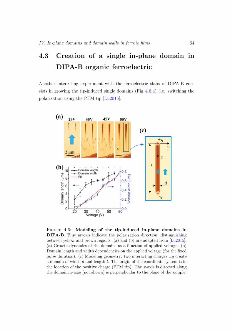
IV. In-plane domains and domain walls in ferroic films 64
4.3 Creation of a single in-plane domain in
DIPA-B organic ferroelectric
Another interesting experiment with the ferroelectric slabs of DIPA-B con-
sists in growing the tip-induced single domains (Fig. 4.6,a), i.e. switching the
polarization using the PFM tip [Lu2015].
(c)
d
l
+q
-q
y
x
Figure 4.6: Modeling of the tip-induced in-plane domains inDIPA-B. Blue arrows indicate the polarization direction, distinguishingbetween yellow and brown regions. (a) and (b) are adapted from [Lu2015].(a) Growth dynamics of the domains as a function of applied voltage. (b)Domain length and width dependencies on the applied voltage (for the fixedpulse duration). (c) Modeling geometry: two interacting charges ±q createa domain of width d and length l. The origin of the coordinate system is inthe location of the positive charge (PFM tip). The x-axis is directed alongthe domain, z-axis (not shown) is perpendicular to the plane of the sample.
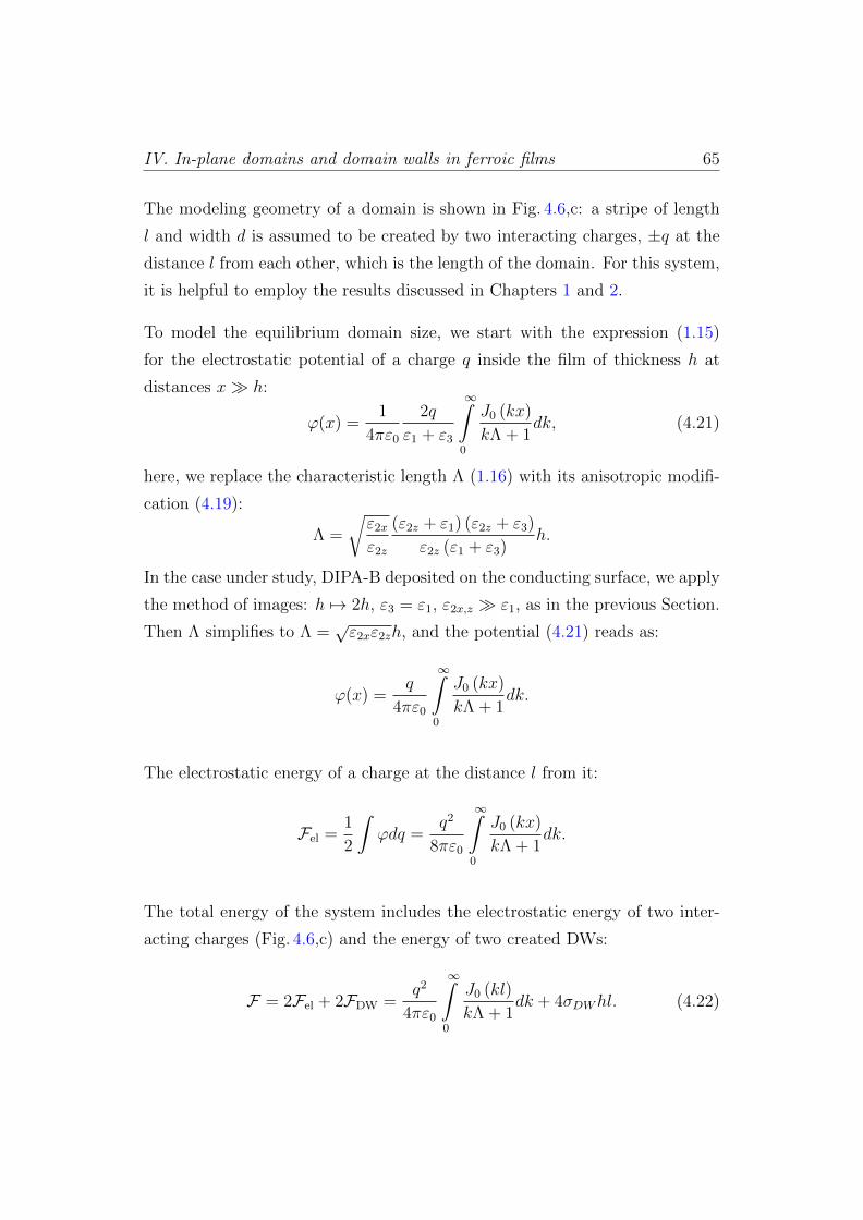
IV. In-plane domains and domain walls in ferroic films 65
The modeling geometry of a domain is shown in Fig. 4.6,c: a stripe of length
l and width d is assumed to be created by two interacting charges, ±q at the
distance l from each other, which is the length of the domain. For this system,
it is helpful to employ the results discussed in Chapters 1 and 2.
To model the equilibrium domain size, we start with the expression (1.15)
for the electrostatic potential of a charge q inside the film of thickness h at
distances x h:
ϕ(x) =1
4πε0
2q
ε1 + ε3
∞∫0
J0 (kx)
kΛ + 1dk, (4.21)
here, we replace the characteristic length Λ (1.16) with its anisotropic modifi-
cation (4.19):
Λ =
√ε2x
ε2z
(ε2z + ε1) (ε2z + ε3)
ε2z (ε1 + ε3)h.
In the case under study, DIPA-B deposited on the conducting surface, we apply
the method of images: h 7→ 2h, ε3 = ε1, ε2x,z ε1, as in the previous Section.
Then Λ simplifies to Λ =√ε2xε2zh, and the potential (4.21) reads as:
ϕ(x) =q
4πε0
∞∫0
J0 (kx)
kΛ + 1dk.
The electrostatic energy of a charge at the distance l from it:
Fel =1
2
∫ϕdq =
q2
8πε0
∞∫0
J0 (kx)
kΛ + 1dk.
The total energy of the system includes the electrostatic energy of two inter-
acting charges (Fig. 4.6,c) and the energy of two created DWs:
F = 2Fel + 2FDW =q2
4πε0
∞∫0
J0 (kl)
kΛ + 1dk + 4σDWhl. (4.22)
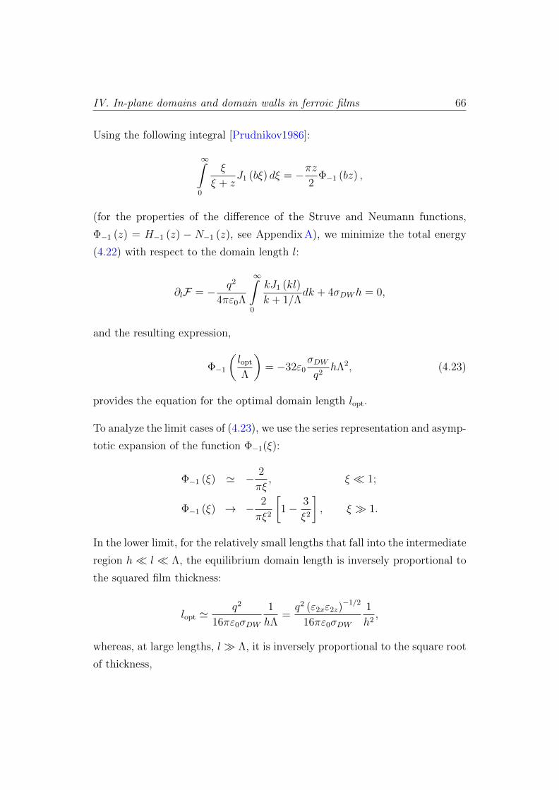
IV. In-plane domains and domain walls in ferroic films 66
Using the following integral [Prudnikov1986]:
∞∫0
ξ
ξ + zJ1 (bξ) dξ = −πz
2Φ−1 (bz) ,
(for the properties of the difference of the Struve and Neumann functions,
Φ−1 (z) = H−1 (z) − N−1 (z), see Appendix A), we minimize the total energy
(4.22) with respect to the domain length l:
∂lF = − q2
4πε0Λ
∞∫0
kJ1 (kl)
k + 1/Λdk + 4σDWh = 0,
and the resulting expression,
Φ−1
(lopt
Λ
)= −32ε0
σDWq2
hΛ2, (4.23)
provides the equation for the optimal domain length lopt.
To analyze the limit cases of (4.23), we use the series representation and asymp-
totic expansion of the function Φ−1(ξ):
Φ−1 (ξ) ' − 2
πξ, ξ 1;
Φ−1 (ξ) → − 2
πξ2
[1− 3
ξ2
], ξ 1.
In the lower limit, for the relatively small lengths that fall into the intermediate
region h l Λ, the equilibrium domain length is inversely proportional to
the squared film thickness:
lopt 'q2
16πε0σDW
1
hΛ=q2 (ε2xε2z)
−1/2
16πε0σDW
1
h2,
whereas, at large lengths, l Λ, it is inversely proportional to the square root
of thickness,
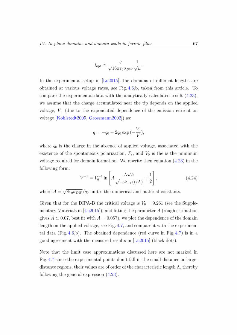
IV. In-plane domains and domain walls in ferroic films 67
lopt 'q√
16πε0σDW
1√h.
In the experimental setup in [Lu2015], the domains of different lengths are
obtained at various voltage rates, see Fig. 4.6,b, taken from this article. To
compare the experimental data with the analytically calculated result (4.23),
we assume that the charge accumulated near the tip depends on the applied
voltage, V , (due to the exponential dependence of the emission current on
voltage [Kohlstedt2005, Grossmann2002]) as:
q = −q0 + 2q0 exp (−V0
V),
where q0 is the charge in the absence of applied voltage, associated with the
existence of the spontaneous polarization, Ps, and V0 is the is the minimum
voltage required for domain formation. We rewrite then equation (4.23) in the
following form:
V −1 = V −10 ln
[A
Λ√h√
−Φ−1 (l/Λ)+
1
2
], (4.24)
where A =√
8ε0σDW/q0 unites the numerical and material constants.
Given that for the DIPA-B the critical voltage is V0 = 9.261 (see the Supple-
mentary Materials in [Lu2015]), and fitting the parameter A (rough estimation
gives A ' 0.07, best fit with A = 0.057), we plot the dependence of the domain
length on the applied voltage, see Fig. 4.7, and compare it with the experimen-
tal data (Fig. 4.6,b). The obtained dependence (red curve in Fig. 4.7) is in a
good agreement with the measured results in [Lu2015] (black dots).
Note that the limit case approximations discussed here are not marked in
Fig. 4.7 since the experimental points don’t fall in the small-distance or large-
distance regions, their values are of order of the characteristic length Λ, thereby
following the general expression (4.23).
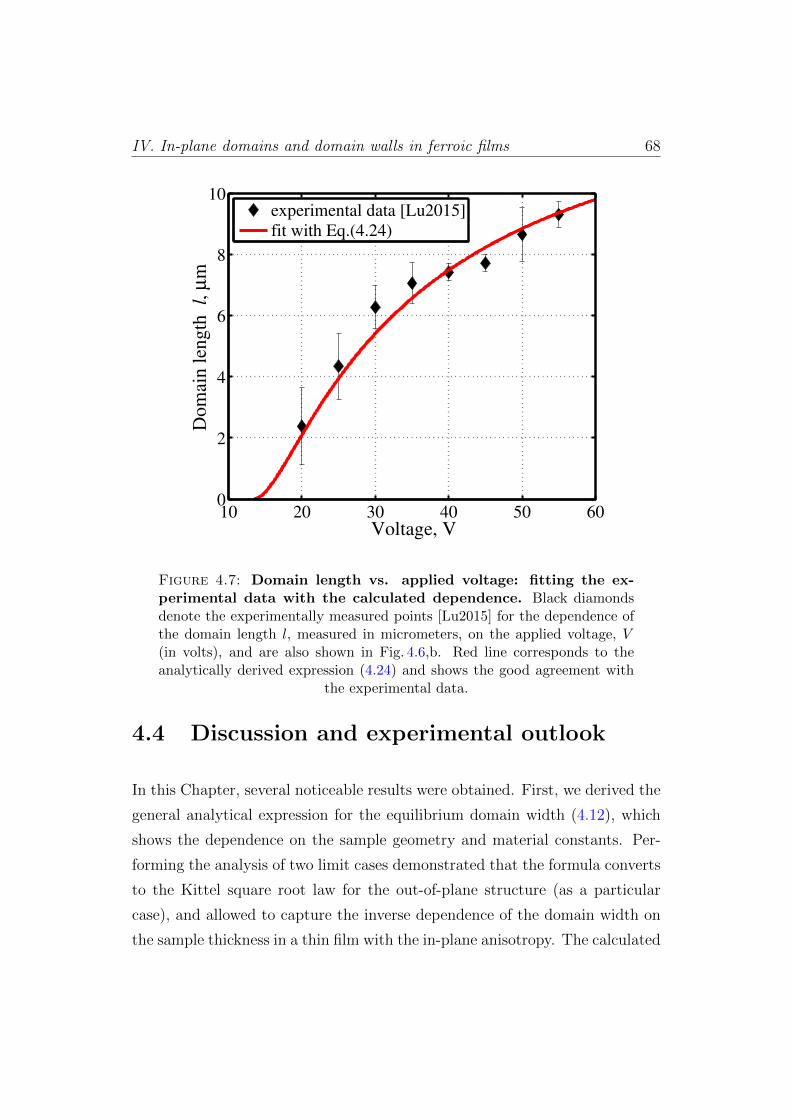
IV. In-plane domains and domain walls in ferroic films 68
Voltage, V
Dom
ain l
ength
l,
µm
10 20 30 40 50 600
2
4
6
8
10experimental data [Lu2015]
fit with Eq.(4.24)
Figure 4.7: Domain length vs. applied voltage: fitting the ex-perimental data with the calculated dependence. Black diamondsdenote the experimentally measured points [Lu2015] for the dependence ofthe domain length l, measured in micrometers, on the applied voltage, V(in volts), and are also shown in Fig. 4.6,b. Red line corresponds to theanalytically derived expression (4.24) and shows the good agreement with
the experimental data.
4.4 Discussion and experimental outlook
In this Chapter, several noticeable results were obtained. First, we derived the
general analytical expression for the equilibrium domain width (4.12), which
shows the dependence on the sample geometry and material constants. Per-
forming the analysis of two limit cases demonstrated that the formula converts
to the Kittel square root law for the out-of-plane structure (as a particular
case), and allowed to capture the inverse dependence of the domain width on
the sample thickness in a thin film with the in-plane anisotropy. The calculated
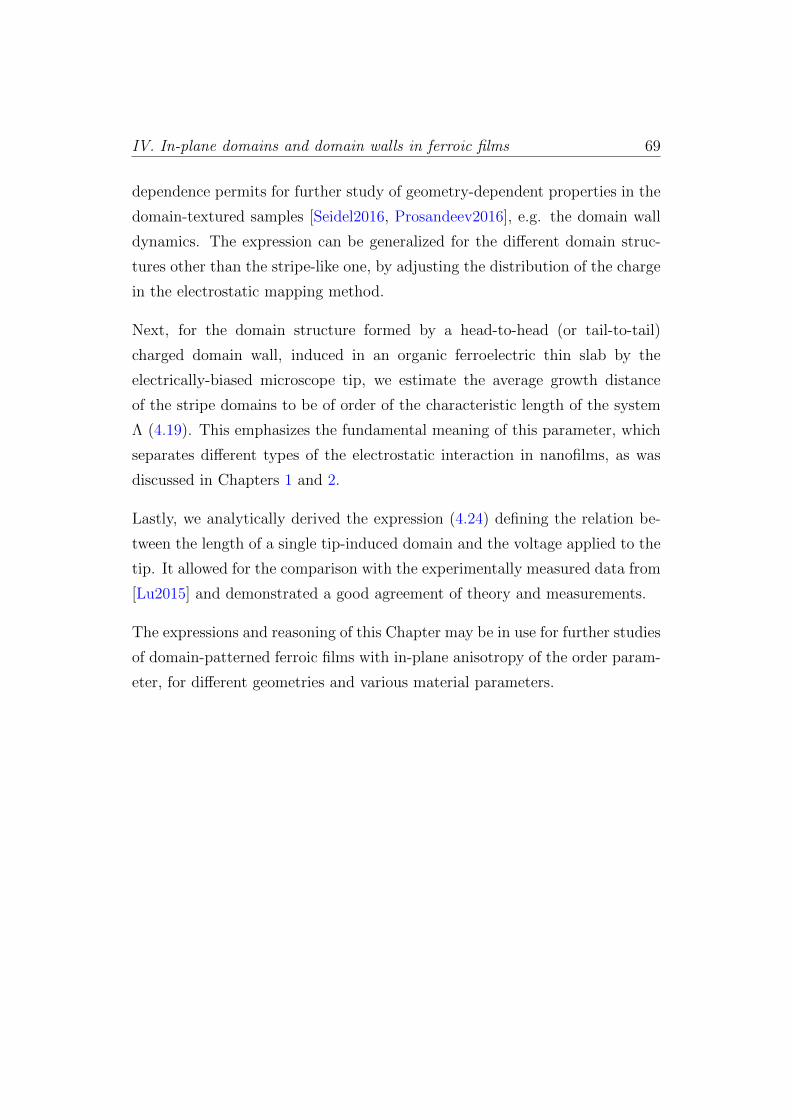
IV. In-plane domains and domain walls in ferroic films 69
dependence permits for further study of geometry-dependent properties in the
domain-textured samples [Seidel2016, Prosandeev2016], e.g. the domain wall
dynamics. The expression can be generalized for the different domain struc-
tures other than the stripe-like one, by adjusting the distribution of the charge
in the electrostatic mapping method.
Next, for the domain structure formed by a head-to-head (or tail-to-tail)
charged domain wall, induced in an organic ferroelectric thin slab by the
electrically-biased microscope tip, we estimate the average growth distance
of the stripe domains to be of order of the characteristic length of the system
Λ (4.19). This emphasizes the fundamental meaning of this parameter, which
separates different types of the electrostatic interaction in nanofilms, as was
discussed in Chapters 1 and 2.
Lastly, we analytically derived the expression (4.24) defining the relation be-
tween the length of a single tip-induced domain and the voltage applied to the
tip. It allowed for the comparison with the experimentally measured data from
[Lu2015] and demonstrated a good agreement of theory and measurements.
The expressions and reasoning of this Chapter may be in use for further studies
of domain-patterned ferroic films with in-plane anisotropy of the order param-
eter, for different geometries and various material parameters.
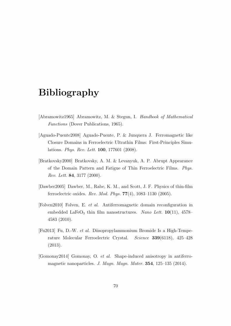
Bibliography
[Abramowitz1965] Abramowitz, M. & Stegun, I. Handbook of Mathematical
Functions (Dover Publications, 1965).
[Aguado-Puente2008] Aguado-Puente, P. & Junquera J. Ferromagnetic like
Closure Domains in Ferroelectric Ultrathin Films: First-Principles Simu-
lations. Phys. Rev. Lett. 100, 177601 (2008).
[Bratkovsky2000] Bratkovsky, A. M. & Levanyuk, A. P. Abrupt Appearance
of the Domain Pattern and Fatigue of Thin Ferroelectric Films. Phys.
Rev. Lett. 84, 3177 (2000).
[Dawber2005] Dawber, M., Rabe, K. M., and Scott, J. F. Physics of thin-film
ferroelectric oxides. Rev. Mod. Phys. 77(4), 1083–1130 (2005).
[Folven2010] Folven, E. et al. Antiferromagnetic domain reconfiguration in
embedded LaFeO3 thin film nanostructures. Nano Lett. 10(11), 4578–
4583 (2010).
[Fu2013] Fu, D.-W. et al. Diisopropylammonium Bromide Is a High-Tempe-
rature Molecular Ferroelectric Crystal. Science 339(6118), 425–428
(2013).
[Gomonay2014] Gomonay, O. et al. Shape-induced anisotropy in antiferro-
magnetic nanoparticles. J. Magn. Magn. Mater. 354, 125–135 (2014).
70
IV. In-plane domains and domain walls in ferroic films 71
[Grossmann2002] Grossmann, M., Lohse, O., Bolten, D., Boettger, U., and
Waser, R. The interface screening model as origin of imprint in
PbZrxTi1−xO3 thin films. II. Numerical simulation and verification. J.
Appl. Phys. 92(5), 2688–2696 (2002).
[Gulyaev2002] Gulyaev Y. V., Zilberman P. E., Elliott R. J., and Epshtein E.
M. Magnetostatic energy and stripe domain structure in a ferromagnetic
plate of finite width with in-plane anisotropy. Phys. Solid State 44(6),
1111–1116 (2002).
[Hruszkewycz2013] Hruszkewycz, S. O., et al. Imaging Local Polarization in
Ferroelectric Thin Films by Coherent X-Ray Bragg Projection Ptychog-
raphy. Phys. Rev. Lett. 110, 177601 (2013).
[Kashuba1993] Kashuba, A., and Pokrovsky, V. L. Stripe Domain Structures
in a Thin Ferromagnetic Film. Phys. Rev. Lett. 70(20), 3155–3158 (1993).
[Kittel1946] Kittel, C. Theory of the structure of ferromagnetic domains in
films and small particles. Phys. Rev. 70(11-12), 965–971 (1946).
[Kittel1949] Kittel, C. Physical theory of ferromagnetic domains. Rev. Mod.
Phys. 21(4), 541–583 (1949).
[Kohlstedt2005] Kohlstedt, H., Pertsev, N. A., Rodriguez Contreras, J., and
Waser, R. Theoretical current-voltage characteristics of ferroelectric tun-
nel junctions. Phys. Rev. B 72(12), 125341 (2005).
[Kornev2004] Kornev, I., Fu, H., and Bellaiche, L. Ultrathin Films of Ferro-
electric Solid Solutions under a Residual Depolarizing Field. Phys. Rev.
Lett. 93, 196104 (2004).
[Landau1935] Landau, L. D. and Lifshitz, E. M. On the theory of the disper-
sion of magnetic permeability in ferromagnetic bodies. Phys. Z. Sowjet.
8, 101–114 (1935).
IV. In-plane domains and domain walls in ferroic films 72
[Landau1984] Landau, L. D., Lifshits, E. M., and Pitaevskii, L. P. Electrody-
namics of continuous media, volume 8. (Pergamon, Oxford [Oxfordshire];
New York, 1984).
[Lu2015] Lu, H., Li, T., Poddar, S., Goit, O., Lipatov, A., Sinitskii, A.,
Ducharme, S., and Gruverman, A. Statics and Dynamics of Ferroelec-
tric Domains in Diisopropylammonium Bromide. Adv. Mater. 27(47),
7832–7838 (2015).
[Luk’yanchuk2009] Luk’yanchuk, I. A., Lahoche, L., and Sene, A. Universal
Properties of Ferroelectric Domains. Phys. Rev. Lett. 102(14), 147601
(2009).
[Luk’yanchuk2014a] Luk’yanchuk, I., Pakhomov, A., Sene, A., Sidorkin, A.,
and Vinokur, V. Terahertz Electrodynamics of 180 Domain Walls in
Thin Ferroelectric Films. https://arxiv.org/abs/1410.3124, 2014.
[Luk’yanchuk2014b] Luk’yanchuk, I., Sharma, P., Nakajima, T., Okamura, S.,
Scott, J. F., and Gruverman, A. High-symmetry polarization domains in
low-symmetry ferroelectrics. Nano Lett. 14(12), 6931–6935 (2014).
[Matzen2014] Matzen, S. et al. Super switching and control of in-plane fer-
roelectric nanodomains in strained thin films. Nat. Commun. 5, 4415
(2014).
[Mokry2004] Mokry, P., Tagantsev, A. K., & Setter, N. Size effect on per-
mittivity in ferroelectric polydomain thin films. Phys. Rev. B 70, 172107
(2004).
[Prosandeev2016] Prosandeev, S. et al. Ferroelectric Vortices and Related Con-
figurations. Nanoscale Ferroelectrics and Multiferroics, 700–728. (John
Wiley & Sons, Ltd, Chichester, UK, 2016).
[Prudnikov1986] Prudnikov, A. P., Brychkov, Yu. A., and Marichev, O. I.
Integrals and Series. (New York, 1986).
IV. In-plane domains and domain walls in ferroic films 73
[Scott2007] Scott, J. F. Applications of Modern Ferroelectrics. Science 315
(5814), 954–959 (2007).
[Seidel2016] Seidel, J., editor. Topological structures in ferroic materials: do-
main walls, vortices and skyrmions. Springer series in materials science,
228. (Springer, Cham, 2016).
[Sene2010] Sene, A. Theory of Domains and Nonuniform Textures in Ferro-
electrics. (University of Picardie Jules Verne, PhD thesis edition, 2010).
[Stephanovich2005] Stephanovich, V. A., Lukyanchuk, I. A. & Karkut, M. G.
Domain-Enhanced Interlayer Coupling in Ferroelectric/ Paraelectric Su-
perlattices. Phys. Rev. Lett. 94, 047601 (2005).
[Streiffer2002] Streiffer, S. K., et al. Observation of Nanoscale 180 Stripe
Domains in Ferroelectric PbTiO3 Thin Films. Phys. Rev. Lett. 89, 067601
(2002).
[Zubko2010] Zubko, P., Stucki, N., Lichtensteiger C., and Triscone, J.-M. X-
Ray Diffraction Studies of 180 Ferroelectric Domains in PbTiO3/SrTiO3
Superlattices under an Applied Electric Field. Phys. Rev. Lett. 104,
187601 (2010).
[Zubko2012] Zubko, P., et al. Electrostatic Coupling and Local Structural
Distortions at Interfaces in Ferroelectric/Paraelectric Superlattices. Nano
Lett. 12, 2846–2851 (2012).
[Zubko2016] Zubko, P., Wojde l J. C., Hadjimichael, M., Fernandez-Pena, S.,
Sene, A., Luk’yanchuk, I., Triscone, J.-M., and Iniguez, J. Negative ca-
pacitance in multidomain ferroelectric superlattices. Nature 534(7608),
524–528 (2016).
Conclusions and main results
The lower dimensionality of the nanosized dielectrics brings up the unique
electrostatic properties. As a pronounced example, we have discussed the
appearance of the two-dimensional logarithmic confinement of the charges in
thin dielectric films, as opposed to the conventional three-dimensional Coulomb
interaction. The overview of this phenomena, along with the relevant notions
and notations, is given in Chapter 1.
The distinctive property of high dielectric permittivity (high-κ) thin films is
the existence of various types of electrostatic interactions between charges.
Depending on the combination of the geometric and material parameters of
the system, the interaction between two charges in a film can either follow
the three-dimensional Coulomb law, or have the two-dimensional logarithmic
character. It is possible to tune the range of interaction with the external
gate electrode; moreover, the presence of the gate in the system unravels the
new interaction types: dipole-like and exponential screening. This remarkable
variety opens a way to further study of related phenomena, including the topo-
logical phase transitions and the scalability and charge-trapping in nanosized
memory elements, and hopefully resulting in the promising applications. The
details of this research are outlined in Chapter 2, in which:
• a theory of the electrostatic behavior of charges in the two-dimensional
high-κ system in the presence of the gate is developed, basing on the
numerical and analytical modeling of the electrostatic potential;
74
Conclusions and main results 75
• the types of the electrostatic interactions, depending on the relations be-
tween the material and geometric parameters of the system, are analyzed
and assembled in Table 2.1 and Fig. 2.6.
The calculations performed in Chapter 2 provide the foundation for the inves-
tigation of the extended charges interacting in thin dielectric and ferroelectric
films. Particularly, in Chapter 3:
• the electrostatic potential of a homogeneously charged wire placed on the
substrate-deposited thin film was calculated for the arbitrary values of
the dielectric constants of the film, substrate and surrounding medium;
• the exact analytical expression for capacitance of the system of two par-
allel wires is derived;
• a method for the determination of the dielectric constant ε of thin films
is proposed, based on the capacitance measurement with the two-wire
capacitor. The limit cases of high-ε and low-ε films are analyzed.
Finally, in Chapter 4, we study the formation of stripe-like in-plane domains
in thin films with in-plane uniaxial anisotropy of the order parameter.
The discontinuity of the order parameter (polarization or magnetization) near
the film edge results in appearance of depolarizing (demagnetizing) fields, thus
enhancing the sample energy, which can make the existence of domains in the
system energetically favourable and lead to the domain structure formation.
To find the equilibrium domain size, we move to the electrostatic problem of a
periodically charged wire or stripe, the linear charge density of which resem-
bles the distribution of the order parameter at the film edge. This maps the
polarization (magnetization) texture of the film on the electrostatic potential
created by the wire or stripe, allowing to extend the methods and calcula-
tions of the previous Chapters on the problem of the in-plane striped domain
structure formation.
Conclusions and main results 76
Another way to obtain the in-plane domains in thin films is to create a domain
wall in the material. For example, the charged domain wall, induced in the
molecular ferroelectric DIPA-B by the tip of piezoresponse force microscope,
causes the appearance of head-to-head (or tail-to-tail, depending on the domain
wall charge) stripe in-plane domains. In another experiment, accumulating
the charge below the microscope tip leads to the growth of a single in-plane
domain, the length and width of which depend on the voltage applied. The
research work performed in Chapter 4 contributes to the theory of the discussed
phenomena, specifically:
• the electrostatic energy of a periodically step-like charged stripe at the
edge of magnetic film (ε=1) is calculated for the arbitrary stripe width,
and the optimal domain size dependence on the sample geometry is de-
rived. The limit cases of the infinitely wide stripe and the thin wire
are analyzed. The former converts to the known Kittel’s out-of-plain
domain structure obeying the square root dependence of the domain pe-
riod on the film thickness, whereas the latter demonstrates the linear
proportionality of the domain period on the films size and the inverse
proportionality on its thickness;
• a model of the appearance of the head-to-head and tail-to-tail domains
near the tip-induced charged domain walls in ferroelectric films with
in-plane polarization is proposed. It is shown that the optimal lateral
distance of domain growth is of order of the characteristic length of the
system, Λ ∼ εh, where ε is the dielectric constant of the material and h
is the film thickness;
• the expression for the dependence of the equilibrium distance of the tip-
induced domain growth on the applied voltage is derived, demonstrating
the good agreement with the experimental data.
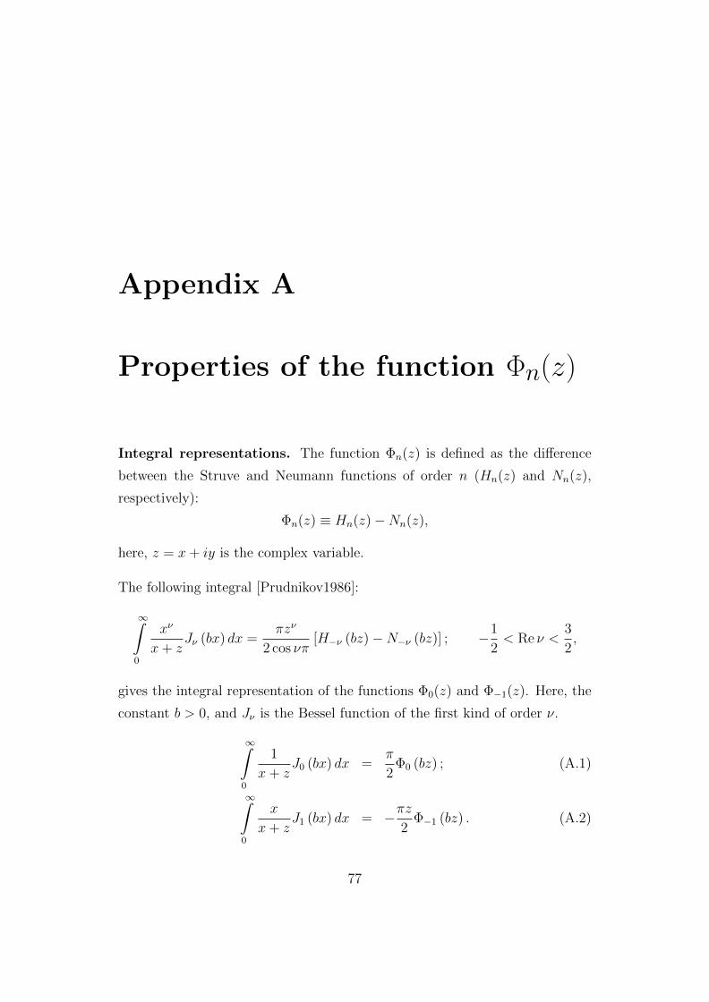
Appendix A
Properties of the function Φn(z)
Integral representations. The function Φn(z) is defined as the difference
between the Struve and Neumann functions of order n (Hn(z) and Nn(z),
respectively):
Φn(z) ≡ Hn(z)−Nn(z),
here, z = x+ iy is the complex variable.
The following integral [Prudnikov1986]:
∞∫0
xν
x+ zJν (bx) dx =
πzν
2 cos νπ[H−ν (bz)−N−ν (bz)] ; −1
2< Re ν <
3
2,
gives the integral representation of the functions Φ0(z) and Φ−1(z). Here, the
constant b > 0, and Jν is the Bessel function of the first kind of order ν.
∞∫0
1
x+ zJ0 (bx) dx =
π
2Φ0 (bz) ; (A.1)
∞∫0
x
x+ zJ1 (bx) dx = −πz
2Φ−1 (bz) . (A.2)
77
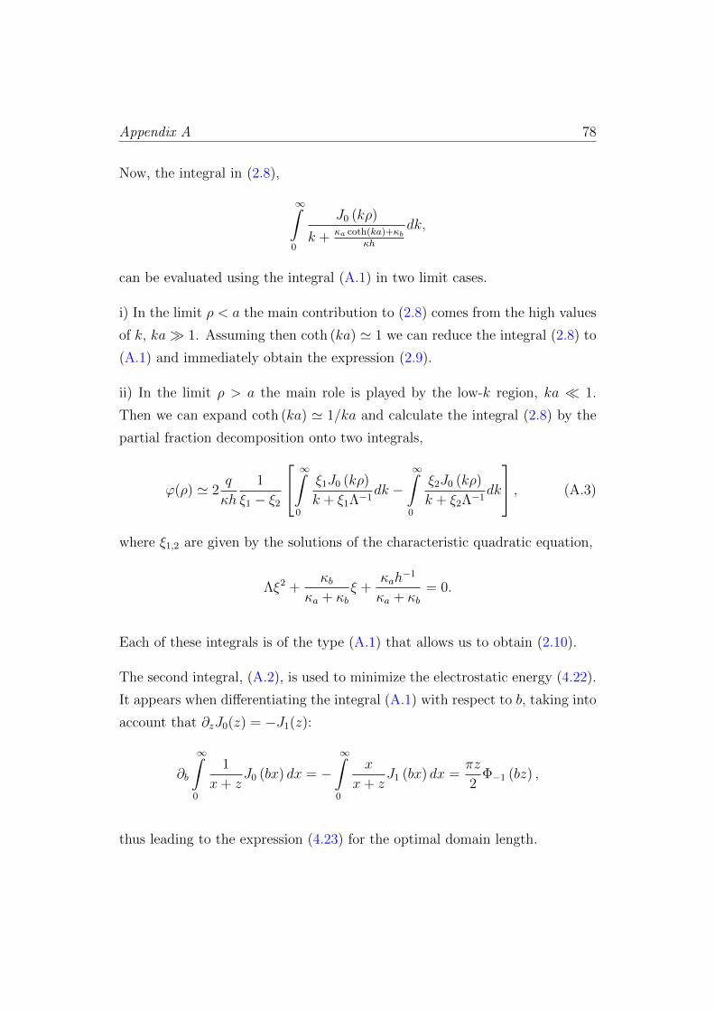
Appendix A 78
Now, the integral in (2.8),
∞∫0
J0 (kρ)
k + κa coth(ka)+κbκh
dk,
can be evaluated using the integral (A.1) in two limit cases.
i) In the limit ρ < a the main contribution to (2.8) comes from the high values
of k, ka 1. Assuming then coth (ka) ' 1 we can reduce the integral (2.8) to
(A.1) and immediately obtain the expression (2.9).
ii) In the limit ρ > a the main role is played by the low-k region, ka 1.
Then we can expand coth (ka) ' 1/ka and calculate the integral (2.8) by the
partial fraction decomposition onto two integrals,
ϕ(ρ) ' 2q
κh
1
ξ1 − ξ2
∞∫0
ξ1J0 (kρ)
k + ξ1Λ−1dk −
∞∫0
ξ2J0 (kρ)
k + ξ2Λ−1dk
, (A.3)
where ξ1,2 are given by the solutions of the characteristic quadratic equation,
Λξ2 +κb
κa + κbξ +
κah−1
κa + κb= 0.
Each of these integrals is of the type (A.1) that allows us to obtain (2.10).
The second integral, (A.2), is used to minimize the electrostatic energy (4.22).
It appears when differentiating the integral (A.1) with respect to b, taking into
account that ∂zJ0(z) = −J1(z):
∂b
∞∫0
1
x+ zJ0 (bx) dx = −
∞∫0
x
x+ zJ1 (bx) dx =
πz
2Φ−1 (bz) ,
thus leading to the expression (4.23) for the optimal domain length.
Appendix A 79
Limit expansions. The series representation for the function of complex
variable Φn(z) can be found from the corresponding properties of Hn and Nn
[Abramowitz1965, Gradshteyn2014]. In the case of zero order function Φ0(z)
it can be approximated at small z as:
Φ0 (z) ' − 2
πlncz
2,
where c = eγ ' 1.781 is the exponent of the Euler constant. The limit expan-
sions for Φ0(z) are also shown in Fig. 1.2.
For small z, the Struve function H−1(z) → 2π, hence the series for the Φ−1(z)
are mainly defined by the Neumann function N−1(z),
Φ−1 (z) ' N−1 (z) ' 2
πz.
At large |z| 1 there exists the asymptotic expansion (here, Γ denotes the
gamma function),
Φn (z)→ 1
π
k−1∑m=0
Γ(m+ 1
2
)(z/2)n−1−2m
√πΓ(n+ 1
2−m
) +O(|z|n−1−2k
).
For example, for the zero order Φ the above expression is reduced to:
Φ0 (z) ' 2
π
(z−1 − z−3
),
which is suitable over the whole complex plane except the vicinity of the imag-
inary axis z = iy, where the real part of this expansion vanishes and the non-
analytic contribution prevails. The latter can be accounted for, by presenting
Re Φ0 (iy) via the Macdonald function K0,
Re Φ0 (iy) =2
πK0 (y) ,
Appendix A 80
that is approximated at y 1 as K0(y) '√
2πye−y.
And finally, for the function Φ−1(z) the asymptotic expansion reads as:
Φ−1 (z)→ − 2
πz2
[1− 3
z2
],
allowing us to analyze the expression for the optimal domain length (4.23).
—————————————————————————————————–
[Abramowitz1965] Abramowitz, M. & Stegun, I. Handbook of Mathematical
Functions (Dover Publications, 1965).
[Gradshteyn2014] Gradshteyn, I. S. & Ryzhik, I. M. Table of integrals, series,
and products (Academic press, 2014).
[Prudnikov1986] Prudnikov, A. P., Brychkov, Yu. A., and Marichev, O. I.,
Integrals and Series (New York, 1986).
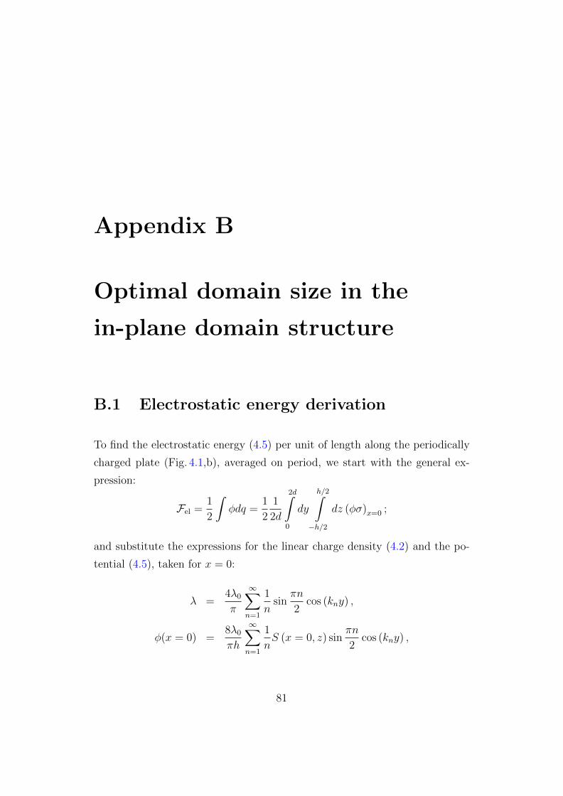
Appendix B
Optimal domain size in the
in-plane domain structure
B.1 Electrostatic energy derivation
To find the electrostatic energy (4.5) per unit of length along the periodically
charged plate (Fig. 4.1,b), averaged on period, we start with the general ex-
pression:
Fel =1
2
∫φdq =
1
2
1
2d
2d∫0
dy
h/2∫−h/2
dz (φσ)x=0 ;
and substitute the expressions for the linear charge density (4.2) and the po-
tential (4.5), taken for x = 0:
λ =4λ0
π
∞∑n=1
1
nsin
πn
2cos (kny) ,
φ(x = 0) =8λ0
πh
∞∑n=1
1
nS (x = 0, z) sin
πn
2cos (kny) ,
81
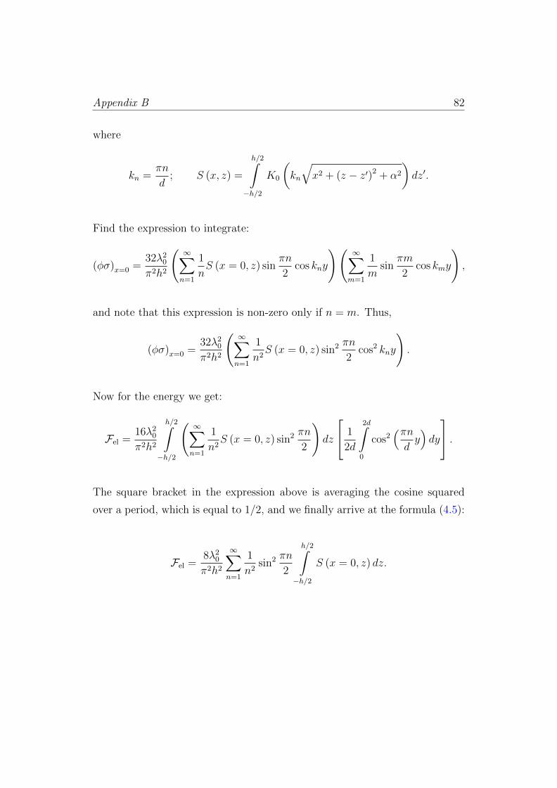
Appendix B 82
where
kn =πn
d; S (x, z) =
h/2∫−h/2
K0
(kn
√x2 + (z − z′)2 + α2
)dz′.
Find the expression to integrate:
(φσ)x=0 =32λ2
0
π2h2
(∞∑n=1
1
nS (x = 0, z) sin
πn
2cos kny
)(∞∑m=1
1
msin
πm
2cos kmy
),
and note that this expression is non-zero only if n = m. Thus,
(φσ)x=0 =32λ2
0
π2h2
(∞∑n=1
1
n2S (x = 0, z) sin2 πn
2cos2 kny
).
Now for the energy we get:
Fel =16λ2
0
π2h2
h/2∫−h/2
(∞∑n=1
1
n2S (x = 0, z) sin2 πn
2
)dz
1
2d
2d∫0
cos2(πndy)dy
.
The square bracket in the expression above is averaging the cosine squared
over a period, which is equal to 1/2, and we finally arrive at the formula (4.5):
Fel =8λ2
0
π2h2
∞∑n=1
1
n2sin2 πn
2
h/2∫−h/2
S (x = 0, z) dz.
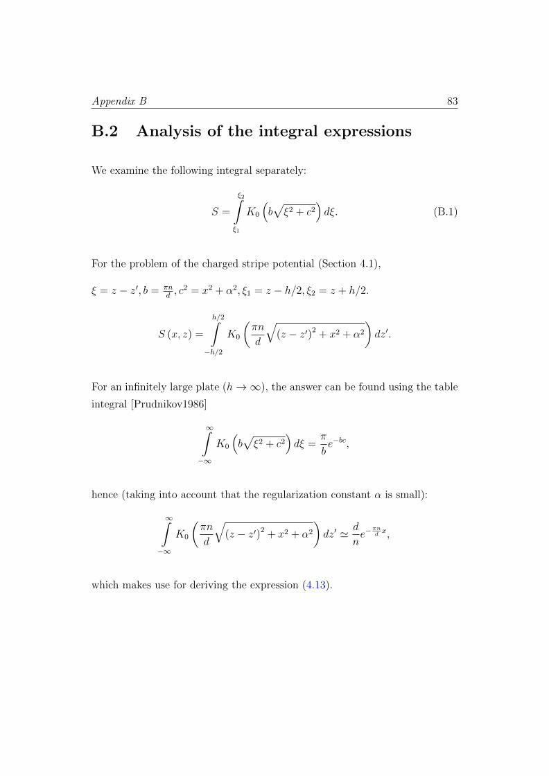
Appendix B 83
B.2 Analysis of the integral expressions
We examine the following integral separately:
S =
ξ2∫ξ1
K0
(b√ξ2 + c2
)dξ. (B.1)
For the problem of the charged stripe potential (Section 4.1),
ξ = z − z′, b = πnd, c2 = x2 + α2, ξ1 = z − h/2, ξ2 = z + h/2.
S (x, z) =
h/2∫−h/2
K0
(πn
d
√(z − z′)2 + x2 + α2
)dz′.
For an infinitely large plate (h→∞), the answer can be found using the table
integral [Prudnikov1986]
∞∫−∞
K0
(b√ξ2 + c2
)dξ =
π
be−bc,
hence (taking into account that the regularization constant α is small):
∞∫−∞
K0
(πn
d
√(z − z′)2 + x2 + α2
)dz′ ' d
ne−
πndx,
which makes use for deriving the expression (4.13).
Appendix B 84
For the case of the finite plate, we can analyze the integral (B.1), using the se-
ries representation of the zero order Macdonald function K0 [Gradshteyn2014]:
K0(s) =∞∑m=0
(s/2)2m
(m!)2
[ψ(m+ 1)− ln
s
2
],
where ψ denotes the digamma function.
Substituting, for our case, s = πnd
√(z − z′)2 + x2 + α2, we can integrate each
term of the sum. For the sake of convenience, note that we are interested in
the integral S (x = 0, z), so take x = 0, c2 = x2 + α2 7→ α2. The result is:
S (x = 0, z) =∞∑k=0
(πnα2d
)2k 1
(k!)2
k∑
m=0
Cmk
(ψ (k + 1)− ln πn
2d
)α2m (2m+ 1)
ξ2m+1+
+k∑
m=0
αCmk
2m+ 1
[(−1)m+1 arctan
ξ
α+
m∑l=0
(−1)l
2m− 2l + 1
(ξ
α
)2m−2l+1]−
− 1
2
k∑m=0
Cmk
α2m (2m+ 1)
[ξ2m+1 ln
(ξ2 + α2
)]∣∣∣∣∣ξ=z+h
2
ξ=z−h2
.
Here, Cmk = k!
m!(k−m)!, and the limits of integration are from ξ = z − h
2to
ξ = z + h2.
The next step is to integrate the obtained expression, which means to find
the electrostatic energy (4.5). At this step, we neglect the terms of order of
the small cutoff parameter α and higher. We end up with a relatively simple
relation:
h/2∫−h/2
S (x = 0, z) dz ' h2
∞∑k=0
(πnh
2d
)2k1
(k!)2
ψ (k + 1)
(2k + 1) (k + 1)−
− 1
2k + 1ln
(πnh
2d
)2
+1
2 (k + 1)ln
(πnh
2d
)2
− 1
2 (k + 1)2 +2
(2k + 1)2
.
Appendix B 85
Having calculated the following sums separately (ξ ≡ πnh2d
):
∞∑k=0
ξ2k
(k + 1) (k!)2 =1
ξI1 (2ξ) ;
∞∑k=0
ξ2k
(k + 1)2 (k!)2 =1
ξ2[I0 (2ξ)− 1] ;
∞∑k=0
ξ2k
(2k + 1) (k!)2 = I0 (2ξ) +π
2I0 (2ξ) L1 (2ξ)− π
2I1 (2ξ) L0 (2ξ) ;
∞∑k=0
ξ2k
(2k + 1)2 (k!)2 =π
2
1
ξ
ξ∫0
[I0 (2t) L1 (2t)− I1 (2t) L0 (2t)] dt+
+1
ξ
ξ∫0
I0 (2t) dt = z2,3
(1
2,1
2; 1,
3
2,3
2; ξ2
);
∞∑k=0
ψ (k + 1) ξ2k
(k + 1) (2k + 1) (k!)2 =I0 (2ξ)− 2
2ξ2− 2z2,3
(1
2,1
2; 1,
3
2,3
2; ξ2
)+
+
[I0 (2ξ)− I1 (2ξ)
2ξ+π
2I0 (2ξ) L1 (2ξ)− π
2I1 (2ξ) L0 (2ξ)
]ln ξ2 −
− 1
4ξG2,1
1,3
(1;−−1
2, 1
2; 0
∣∣∣∣∣ ξ2
),
substituting them, we arrive at the result (4.6), kn = πnd
:
h/2∫−h/2
S (x = 0, z) dz ≈ −h2
[2
k2nh
2+
1
2knhG2,1
1,3
(1;−−1
2, 1
2; 0
∣∣∣∣∣ k2nh
2
4
)].
Notations: Iν is the modified Bessel function of order ν; Lν is the modified
Struve function or order ν; zp,q – the hypergeometric function, G2,11,3 is the
Meijer G-function (see Fig. 4.3). For the properties of the mentioned functions
see [Abramowitz1965].
Appendix B 86
B.3 Total energy minimization and the opti-
mal domain size
To find the equilibrium domain width, let us differentiate the total energy
(4.11) with respect to the domain structure half-period d and equate it to
zero:
∂d (2Fel + FDW) = 0.
Find the derivatives of two energies separately. The electrostatic energy is
given by (4.9):
Fel = −4λ20
π2
∞∑n=1
1
n2sin2 πn
2
[(2d
πnh
)2
+d
πnhG2,1
1,3
(1;−−1
2, 1
2; 0
∣∣∣∣∣(πnh
2d
)2)]
.
Here, G2,11,3 is the Meijer G-function (see Fig. 4.3). Making use of its property
[Abramowitz1965]:
∂ξG2,11,3
(1;−−1
2, 1
2; 0
∣∣∣∣∣ ξ2
)=
2
ξG2,0
0,2
(−−1
2, 1
2
∣∣∣∣∣ ξ2
)=
4
ξK1 (2ξ) ,
with K1 being the first order modified Bessel function of the second kind
(Macdonald function), we find that:
∂dFel = −16λ20
π3h
∞∑n=1
1
n3sin2 πn
2
[2
knh+
1
4G(k2nh
2
4
)−K1 (knh)
].
Here, kn = πnhd
, and G(k2nh
2
4
)≡ G2,1
1,3
(1;−−1
2, 1
2; 0
∣∣∣∣∣ k2nh24
).
For the energy of the domain wall (4.10) we get:
∂dFDW = −σDWlh
d2.
Appendix B 87
Hence, the minimization of the total energy results in the following equation
for the optimal domain width dopt:
32λ20
π3h
∞∑n=1
1
n3f (knh) sin2 πn
2− σDW
lh
d2opt
= 0,
where kn = πnhdopt
and we use the notation
f (knh) = K1 (knh)− 2
knh− 1
4G(k2nh
2
4
).
Thus we arrived to the result (4.12):
d2opt
∞∑n=1
1
n3f
(πnh
dopt
)sin2 πn
2=π3h2σDW
32λ20
l.
—————————————————————————————————–
[Abramowitz1965] Abramowitz, M. & Stegun, I. Handbook of Mathematical
Functions (Dover Publications, 1965).
[Gradshteyn2014] Gradshteyn, I. S. & Ryzhik, I. M. Table of integrals, series,
and products (Academic press, 2014).
[Prudnikov1986] Prudnikov, A. P., Brychkov, Yu. A., and Marichev, O. I.,
Integrals and Series (New York, 1986).
Related Documents