Cyrous Rostamzadeh, Senior IEEE Member, February 17, 2011 Electrostatic Discharge Analysis of Multi Layer Ceramic Capacitors Cyrous Rostamzadeh, Robert Bosch LLC – USA February 17, 2011

Welcome message from author
This document is posted to help you gain knowledge. Please leave a comment to let me know what you think about it! Share it to your friends and learn new things together.
Transcript
Cyrous Rostamzadeh, Senior IEEE Member, February 17, 2011
Electrostatic Discharge Analysis of Multi Layer Ceramic
Capacitors
Cyrous Rostamzadeh, Robert Bosch LLC – USAFebruary 17, 2011

Cyrous Rostamzadeh, Senior IEEE Member, February 17, 2011
Mr. Kimball WilliamsThank you for your Colossal Contributions and Dedication to
IEEE EMC Society.You have educated, trained, inspired, managed and encouraged
many of the EMC Engineers and Technicians in the SE Michigan area.
You are well respected by everyone throughout the EMC Society and Automotive Community.
I had the privilege to prepare this presentation, per your invitation, and I hope you will continue to guide the EMC Society long after your retirement from the Professional
Responsibilities as of February 2012, thank you.

Cyrous Rostamzadeh, Senior IEEE Member, February 17, 2011
Mr. Kimball Williams
Cyrous Rostamzadeh, Senior IEEE Member, February 17, 2011
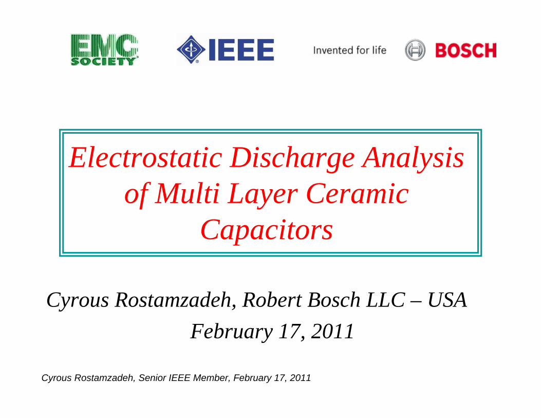
A privilege for me to be educated, mentored, collaborated
with some of the finest minds of EMC…

Cyrous Rostamzadeh, Senior IEEE Member, February 17, 2011
Dr.Clayton Paul
Dr. Al Reuhli (IBM)

Cyrous Rostamzadeh, Senior IEEE Member, February 17, 2011
2001
1994
Dr. Howard JohnsonSignal Integrity

Cyrous Rostamzadeh, Senior IEEE Member, February 17, 2011
Professor Flavio CanaveroPolitecnico di Torino
Professor Christos ChristopouplosUniversity of Nottingham

Cyrous Rostamzadeh, Senior IEEE Member, February 17, 2011
Professor Sergio PignariPolitecnico di Milano
Professor Farhad RachidiSwiss Federal Institute of Technology (EPFL)
Cyrous Rostamzadeh, Senior IEEE Member, February 17, 2011
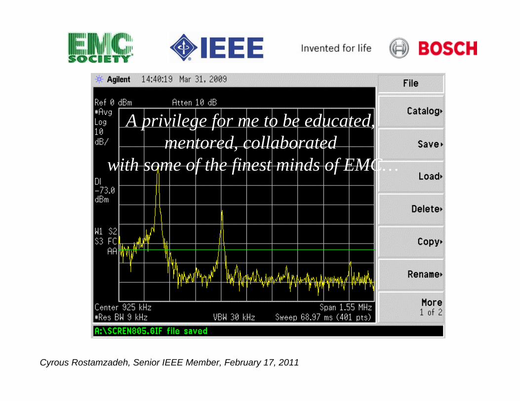
Professor James DrewniakProfessor James DrewniakMissouri ST UniversityMissouri ST University
Professor David PommerenkeProfessor David PommerenkeMissouri ST UniversityMissouri ST University
Dr. Bruce Archambeault Dr. Bruce Archambeault IBM, RTPIBM, RTP
Henry Henry OttOtt
Cyrous Rostamzadeh, Senior IEEE Member, February 17, 2011
Gordon Mapes, Phil Bator, Andy Macko, Mike Bosley,Arnie Nielsen,Gordon Mapes, Phil Bator, Andy Macko, Mike Bosley,Arnie Nielsen,Terry North, Victor Lau, Mark Steffka, Kimball Williams, Howard Terry North, Victor Lau, Mark Steffka, Kimball Williams, Howard Kendall, Don Seyerle, Rick Grunow, Jim Muccioli, Thorsten SchneiKendall, Don Seyerle, Rick Grunow, Jim Muccioli, Thorsten Schneider, der, Tom Livernois, Rick Lombardi, Richard Wiese, Bill Sperber, ScottTom Livernois, Rick Lombardi, Richard Wiese, Bill Sperber, Scott Lytle, Lytle, Keith Frazier, Lloyd Elsworth, Laura Ball, Larry Banasky, Larry Keith Frazier, Lloyd Elsworth, Laura Ball, Larry Banasky, Larry J. J. Boguslawski, Chingchi Chen, Samuel R. Connor, Prof. Marcello Boguslawski, Chingchi Chen, Samuel R. Connor, Prof. Marcello D'Amore, Dr. Phil Fanson, Bill Gilmore, Poul Anderson, Dr. FlaviD'Amore, Dr. Phil Fanson, Bill Gilmore, Poul Anderson, Dr. Flavia a Grassi, Dr. Todd Hubing, Dr. Chris Holloway, Professor Michel IaGrassi, Dr. Todd Hubing, Dr. Chris Holloway, Professor Michel Ianoz, noz, Dr. Thomas A. Jerse, Rob Kado, Richard Kautz, Jarek Tracz, JackDr. Thomas A. Jerse, Rob Kado, Richard Kautz, Jarek Tracz, Jack King, King, Joe Kramer, Roy Leventhal, Filippo Marliani, Scott Mee, Prof. AnJoe Kramer, Roy Leventhal, Filippo Marliani, Scott Mee, Prof. Antonio tonio Orlandi, Vipul Patel, Sreeniwas Ranganathan, Andrew J. Shune, JaOrlandi, Vipul Patel, Sreeniwas Ranganathan, Andrew J. Shune, James mes P. Spivey, John P. Sundeen, Daniel M Traynor, Dr. Al Wexler, Dr.P. Spivey, John P. Sundeen, Daniel M Traynor, Dr. Al Wexler, Dr. David David Hill, Dr. Perry Wilson, Doug Smith, Dr. Erping Li, Dustin WillimHill, Dr. Perry Wilson, Doug Smith, Dr. Erping Li, Dustin Willim, Mark , Mark Wisnewski, Matthew Yager, Paul Sarna, Jack Meyer, Mark MilesWisnewski, Matthew Yager, Paul Sarna, Jack Meyer, Mark Miles……
Cyrous Rostamzadeh, Senior IEEE Member, February 17, 2011
Back to basics…
Electric Currents
Cyrous Rostamzadeh, Senior IEEE Member, February 17, 2011
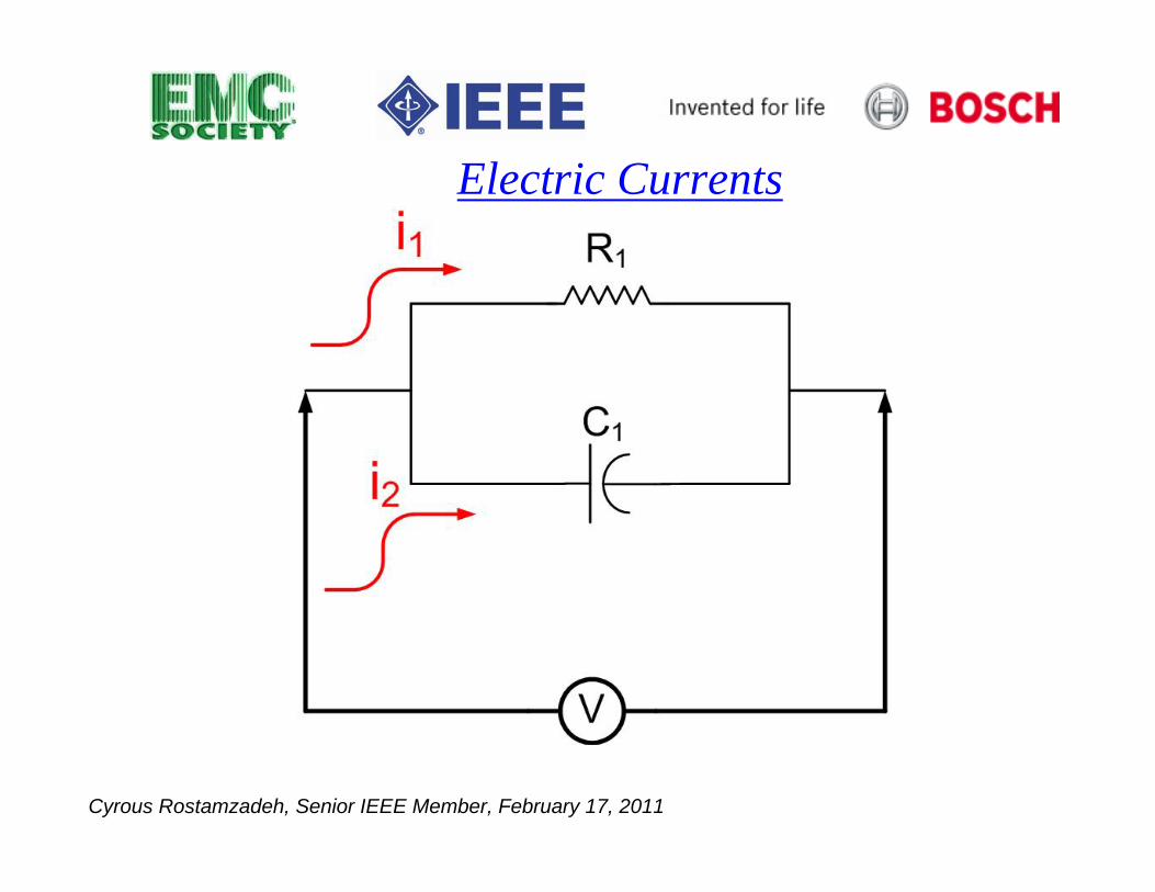
Electric Currents
Cyrous Rostamzadeh, Senior IEEE Member, February 17, 2011
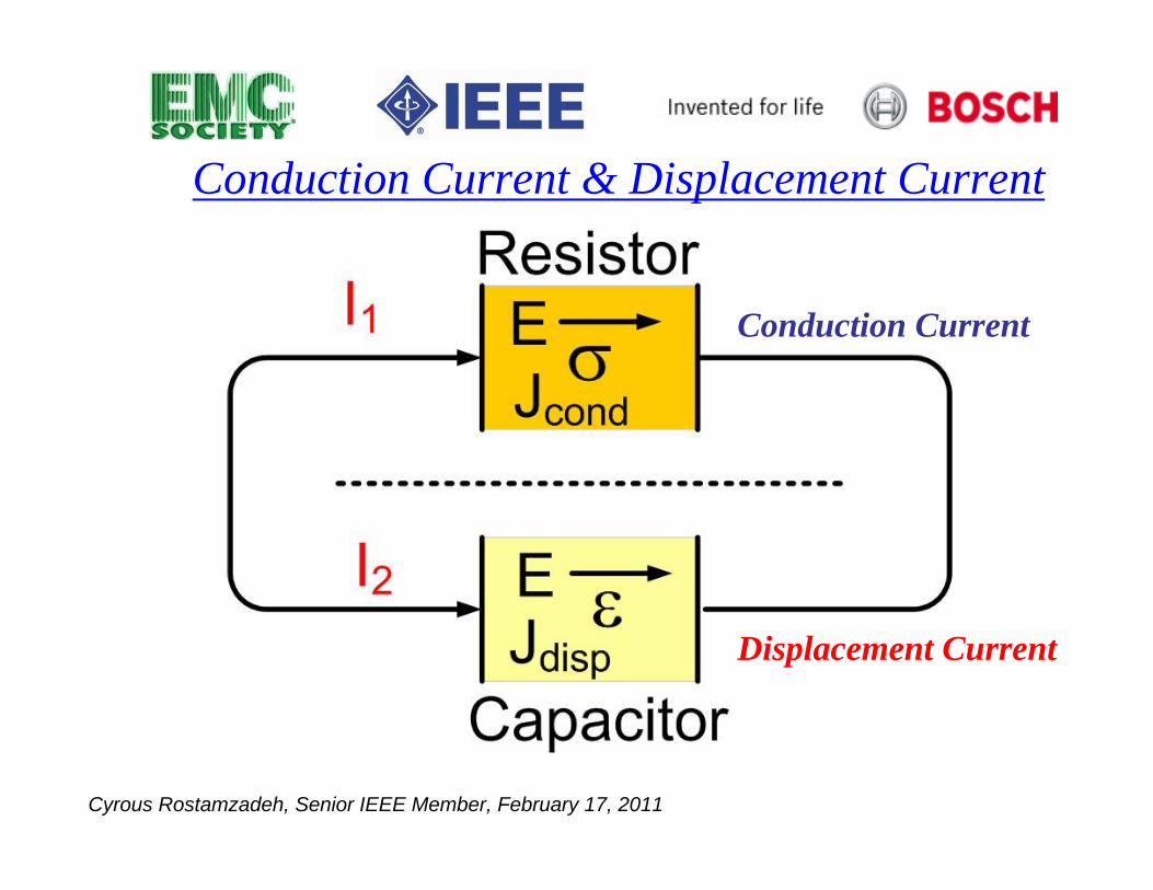
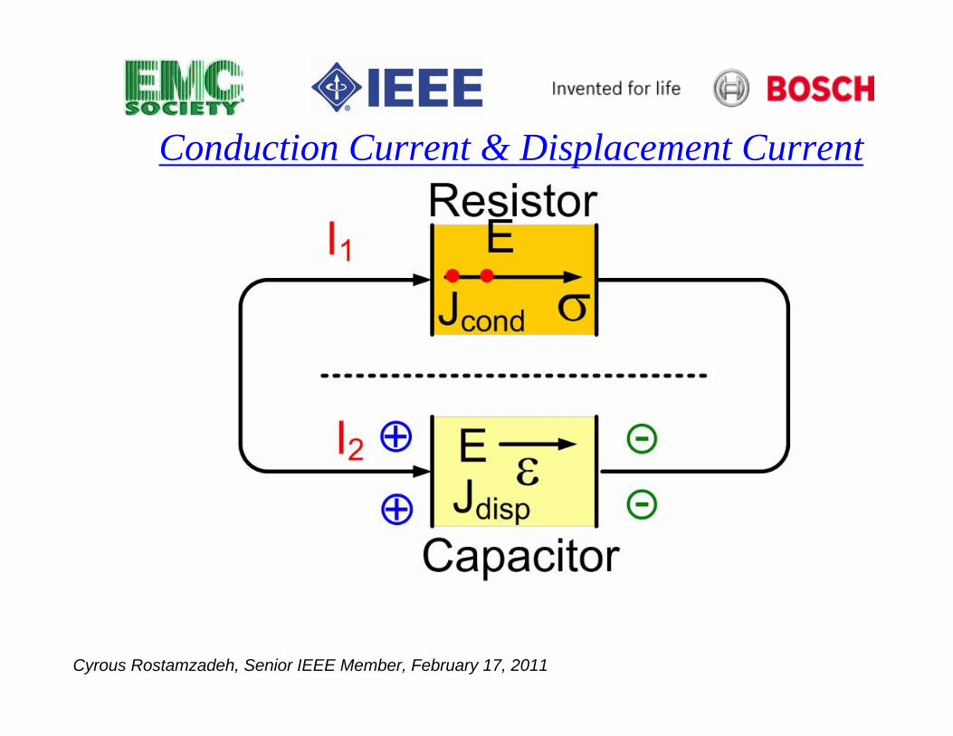
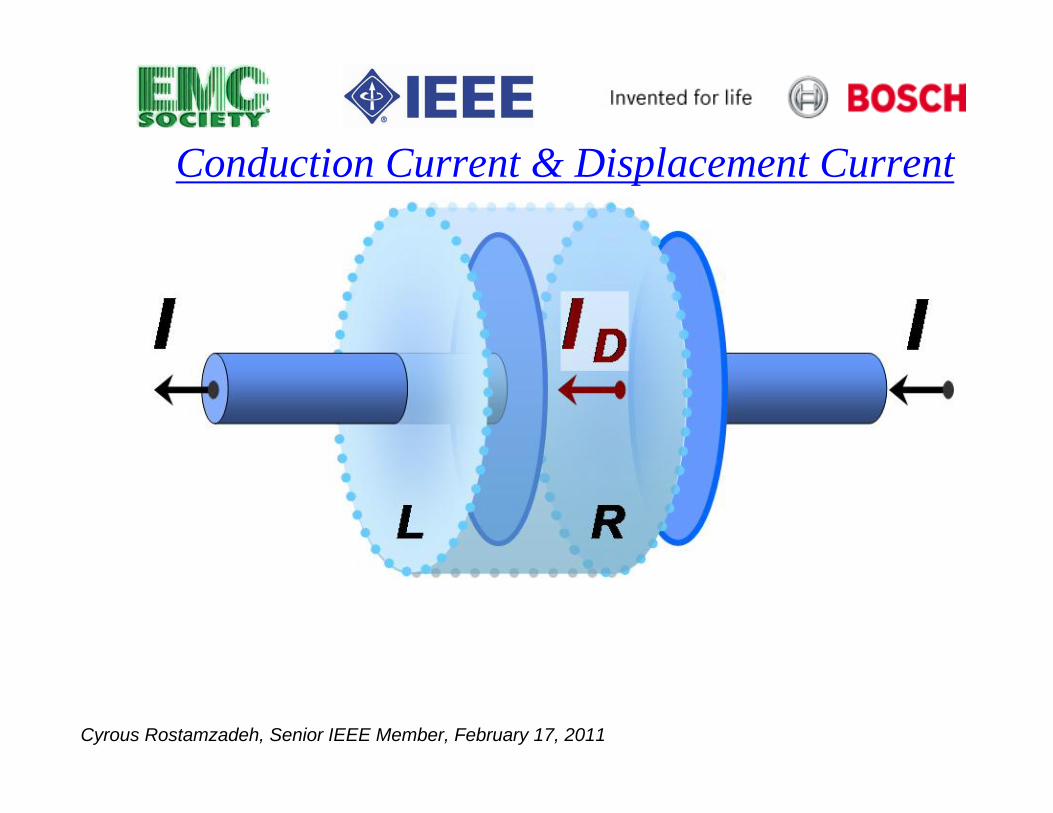
Conduction Current
Displacement Current
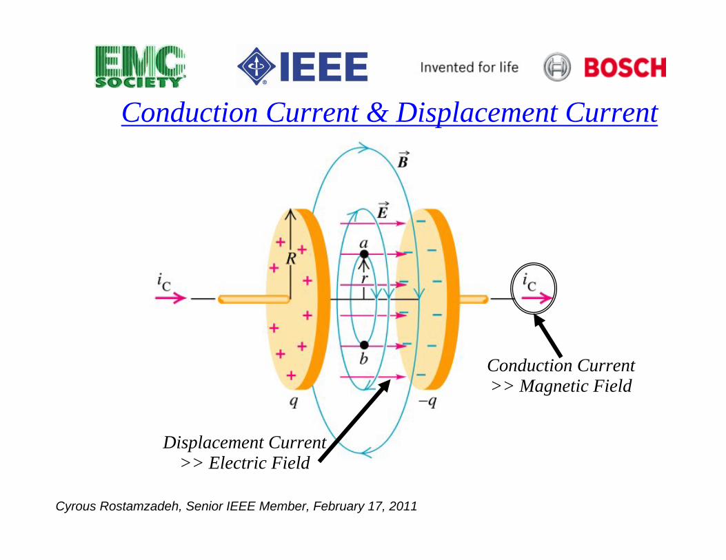
Conduction Current & Displacement Current
Cyrous Rostamzadeh, Senior IEEE Member, February 17, 2011
Conduction Current & Displacement Current
Cyrous Rostamzadeh, Senior IEEE Member, February 17, 2011
Conduction Current & Displacement Current
Cyrous Rostamzadeh, Senior IEEE Member, February 17, 2011
Conduction Current & Displacement Current
Conduction Current >> Magnetic Field
Displacement Current >> Electric Field

Cyrous Rostamzadeh, Senior IEEE Member, February 17, 2011
Motivation and ObjectivesMulti layer Ceramic Capacitors are utilized for ESD
Protection of Connector I/O Pins→ Low Cost, Small Footprint (i.e., 0603 - X7R Class II) ideal for High Density Electronic Control Modules.
ButNeed to determine ESD Robustness or any Degradation due to ESD:
Pre_ESD and Post_ESD Impedance vs. Frequency Characterization. Optical Examination of Dielectric Structure after ESD Exposure.
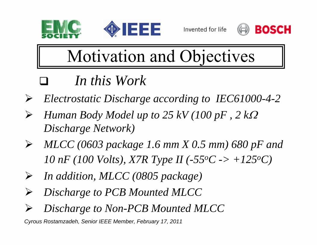
Cyrous Rostamzadeh, Senior IEEE Member, February 17, 2011
Motivation and ObjectivesIn this Work
Electrostatic Discharge according to IEC61000-4-2Human Body Model up to 25 kV (100 pF , 2 kΩDischarge Network)MLCC (0603 package 1.6 mm X 0.5 mm) 680 pF and 10 nF (100 Volts), X7R Type II (-55oC -> +125oC)In addition, MLCC (0805 package)Discharge to PCB Mounted MLCCDischarge to Non-PCB Mounted MLCC

Cyrous Rostamzadeh, Senior IEEE Member, February 17, 2011
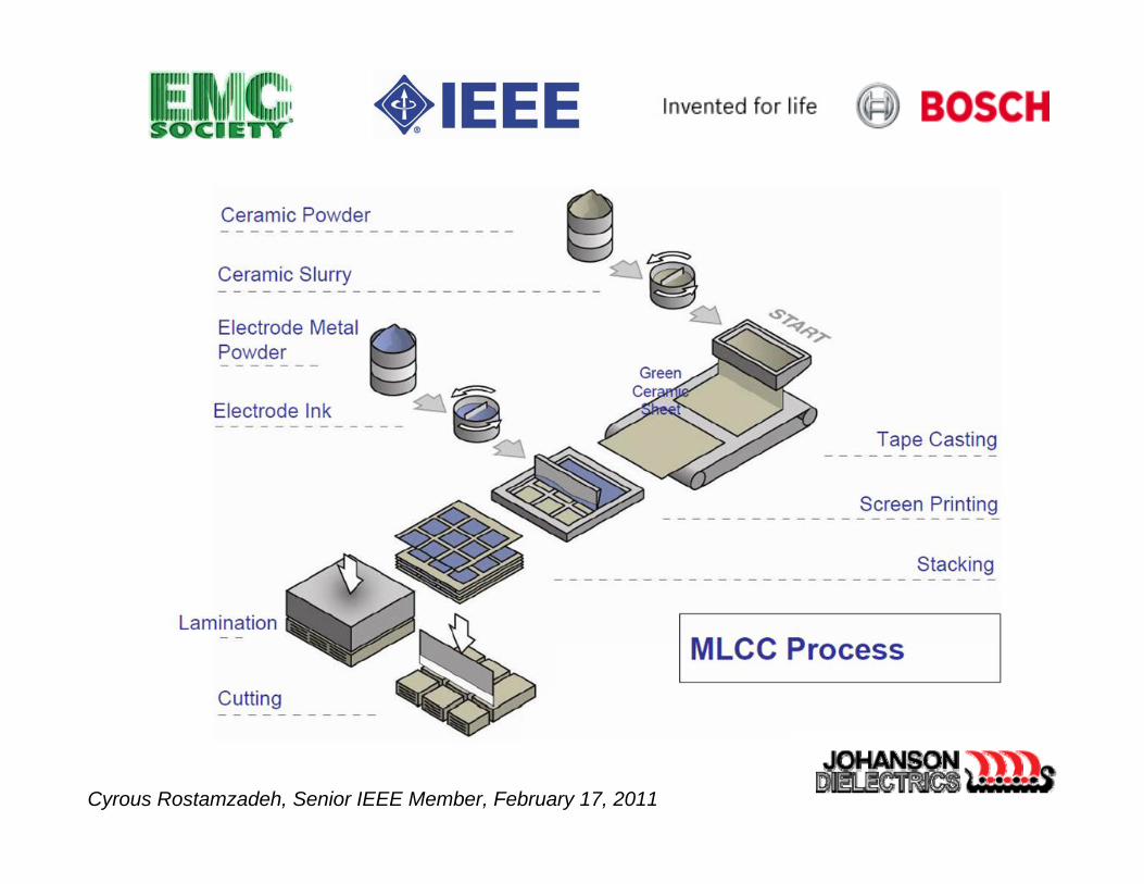
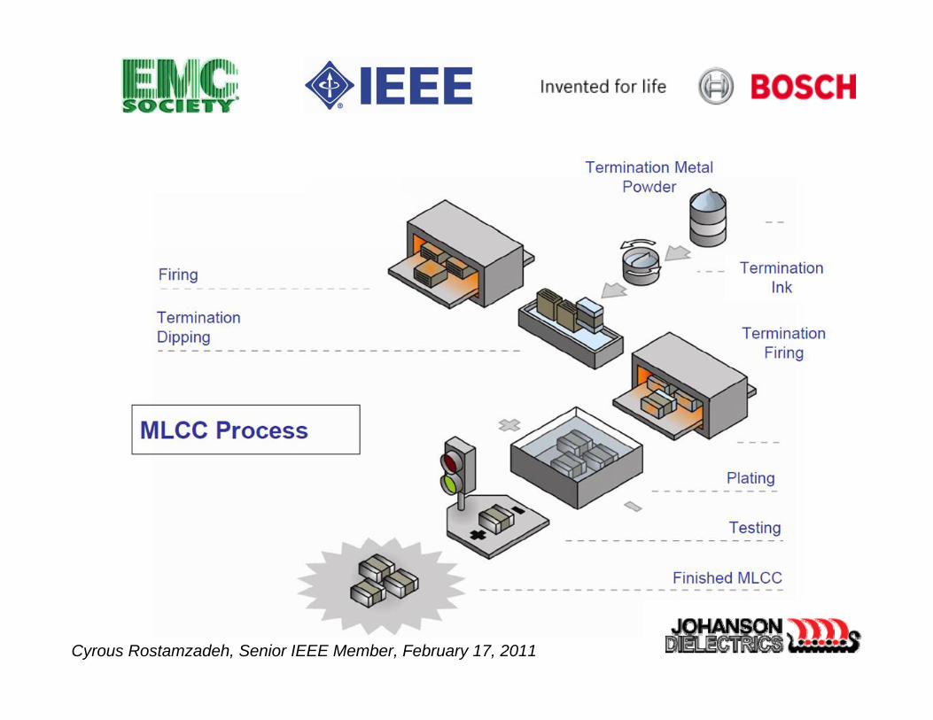
MLCC ProcessMLCC Process
Cyrous Rostamzadeh, Senior IEEE Member, February 17, 2011
Cyrous Rostamzadeh, Senior IEEE Member, February 17, 2011
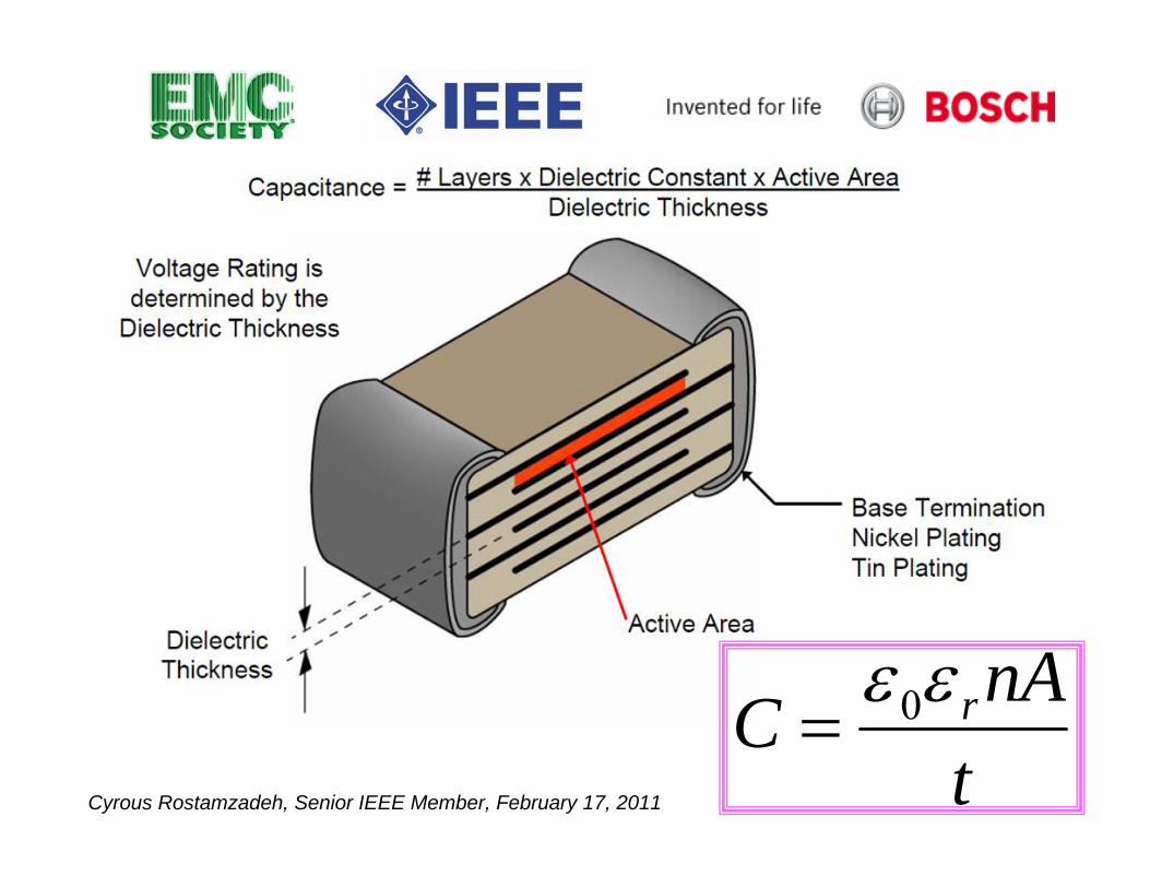
Cyrous Rostamzadeh, Senior IEEE Member, February 17, 2011 tnAC rεε 0=
Cyrous Rostamzadeh, Senior IEEE Member, February 17, 2011

Cyrous Rostamzadeh, Senior IEEE Member, February 17, 2011

Cyrous Rostamzadeh, Senior IEEE Member, February 17, 2011
Ceramic MLCC TypesCeramic MLCC TypesC0G, X7R, X5R, X8R, X8LC0G, X7R, X5R, X8R, X8L
Class I – Most stable over Temperature and Voltage, & Frequency but Lowest Volumetric Efficiency (C0G or NPOC0G or NPO)
Class II – Lower Accuracy and Stability (+/- 15%, -55 0C –> 125 0C)X7RX7R
Class III – Highest Volumetric Efficiency, but Poor Accuracy & Stability
Cyrous Rostamzadeh, Senior IEEE Member, February 17, 2011
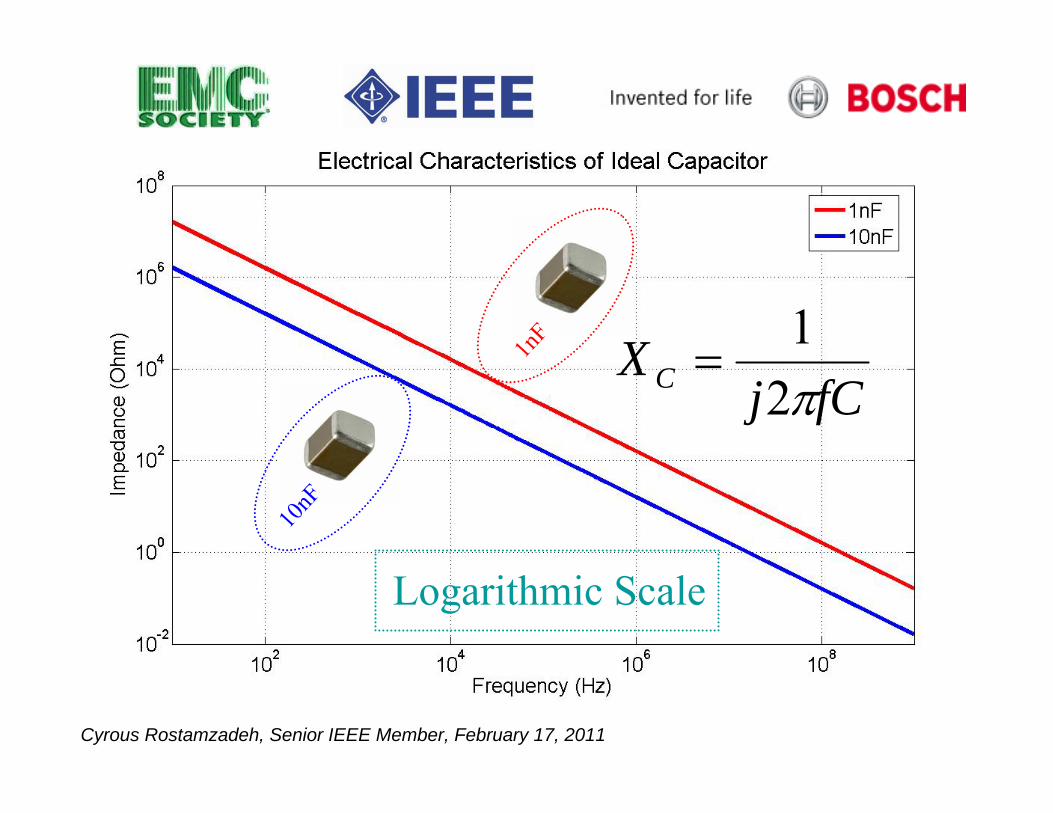
MLCC CharacteristicsMLCC Characteristics
An Electrical ModelAn Electrical Model……
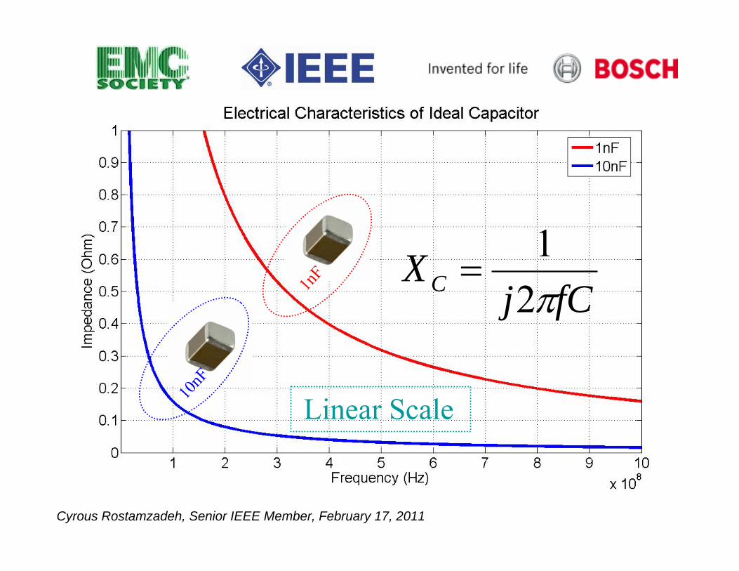
Cyrous Rostamzadeh, Senior IEEE Member, February 17, 2011
1nF
10nF
Linear Scale
fCjX C π2
1=
Cyrous Rostamzadeh, Senior IEEE Member, February 17, 2011
1nF
10nF
Logarithmic Scale
fCjX C π2
1=

Cyrous Rostamzadeh, Senior IEEE Member, February 17, 2011
fCjX C π2
1=
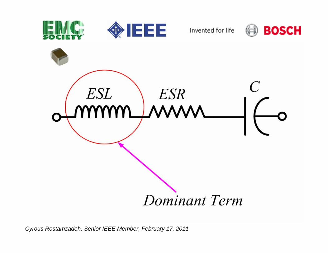
What is in a ModelWhat is in a Model……C
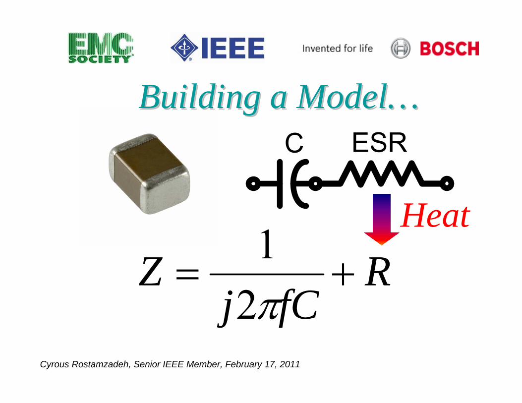
Cyrous Rostamzadeh, Senior IEEE Member, February 17, 2011
RfCj
Z +=π21
Building a ModelBuilding a Model……
Heat

Cyrous Rostamzadeh, Senior IEEE Member, February 17, 2011
fLjRfCj
Z ππ
221
++=
Building a ModelBuilding a Model……
Heat
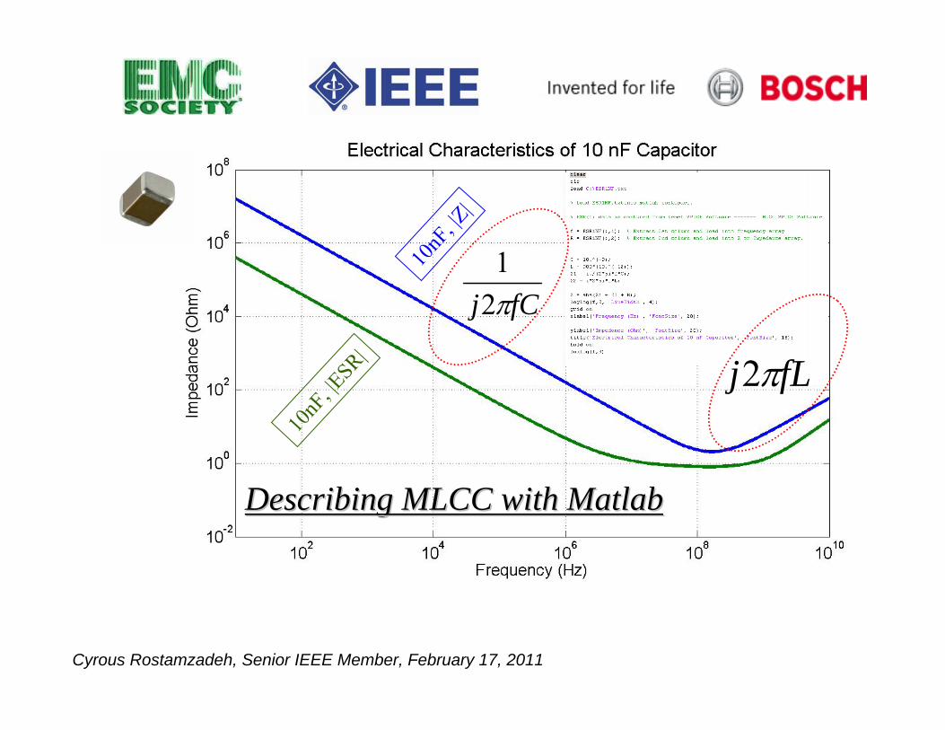
Cyrous Rostamzadeh, Senior IEEE Member, February 17, 2011
10nF
, |Z|
10nF
, |ESR|
fCj π21
fLj π2
Describing MLCC with MatlabDescribing MLCC with Matlab
Cyrous Rostamzadeh, Senior IEEE Member, February 17, 2011
10 mΩ
100 mΩ
1 nF Superior for freq. > 50 MHz
0603 (100 V) MLCC Characteristics
Cyrous Rostamzadeh, Senior IEEE Member, February 17, 2011

Cyrous Rostamzadeh, Senior IEEE Member, February 17, 2011
CjX−δ
Dissipation FactorDissipation Factor
ESR
Impedance PlaneImpedance Plane
QXESRDF
C
1)tan( === δ
DF = Resistive power Loss in ESR / Reactive Power oscillating inDF = Resistive power Loss in ESR / Reactive Power oscillating in CapacitorCapacitor
Loss

Cyrous Rostamzadeh, Senior IEEE Member, February 17, 2011
ESR is a function of FrequencyESR is a function of Frequency
Cyrous Rostamzadeh, Senior IEEE Member, February 17, 2011
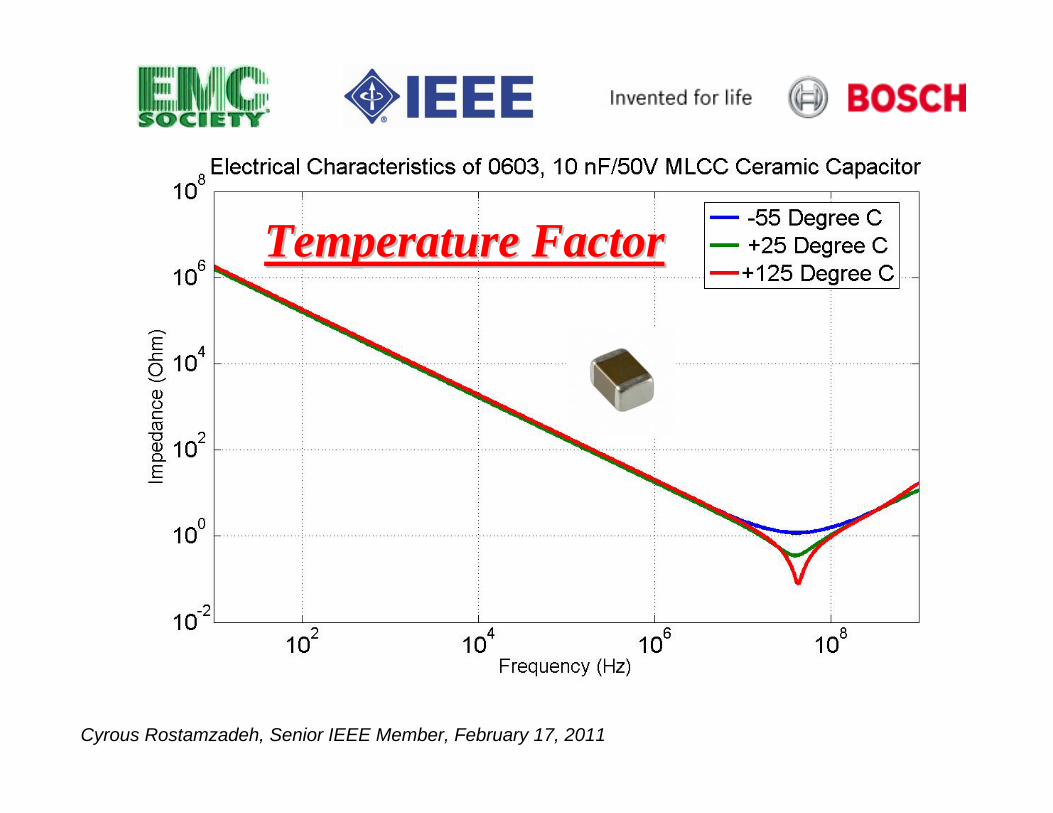
Temperature FactorTemperature Factor

Cyrous Rostamzadeh, Senior IEEE Member, February 17, 2011
an ESD Eventan ESD Event……
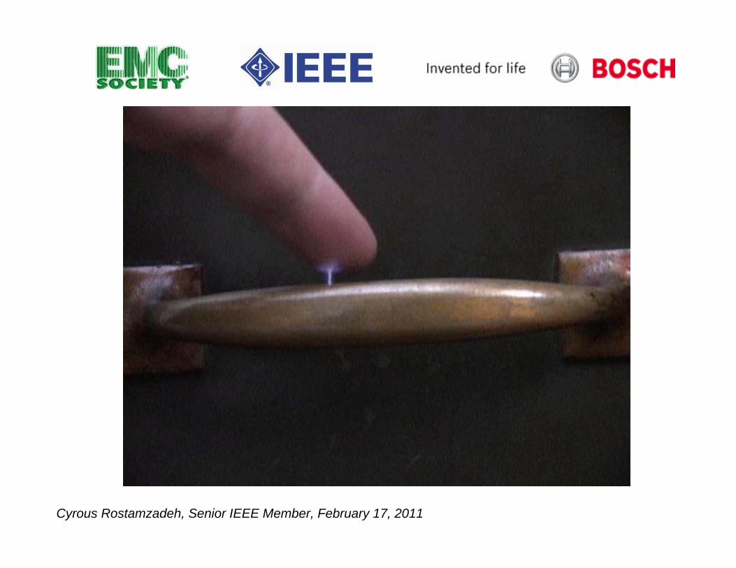
Cyrous Rostamzadeh, Senior IEEE Member, February 17, 2011
Cyrous Rostamzadeh, Senior IEEE Member, February 17, 2011
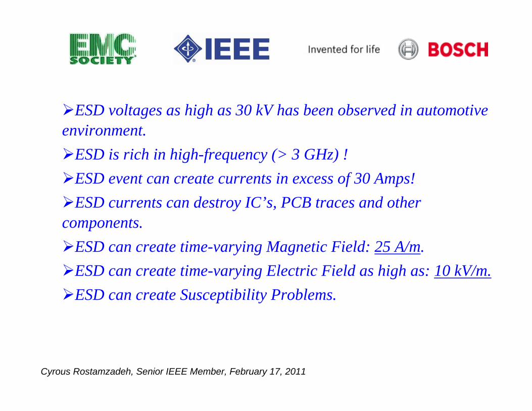
ESD voltages as high as 30 kV has been observed in automotive environment.
ESD is rich in high-frequency (> 3 GHz) !ESD event can create currents in excess of 30 Amps!ESD currents can destroy IC’s, PCB traces and other
components.ESD can create time-varying Magnetic Field: 25 A/m.ESD can create time-varying Electric Field as high as: 10 kV/m.ESD can create Susceptibility Problems.
Cyrous Rostamzadeh, Senior IEEE Member, February 17, 2011
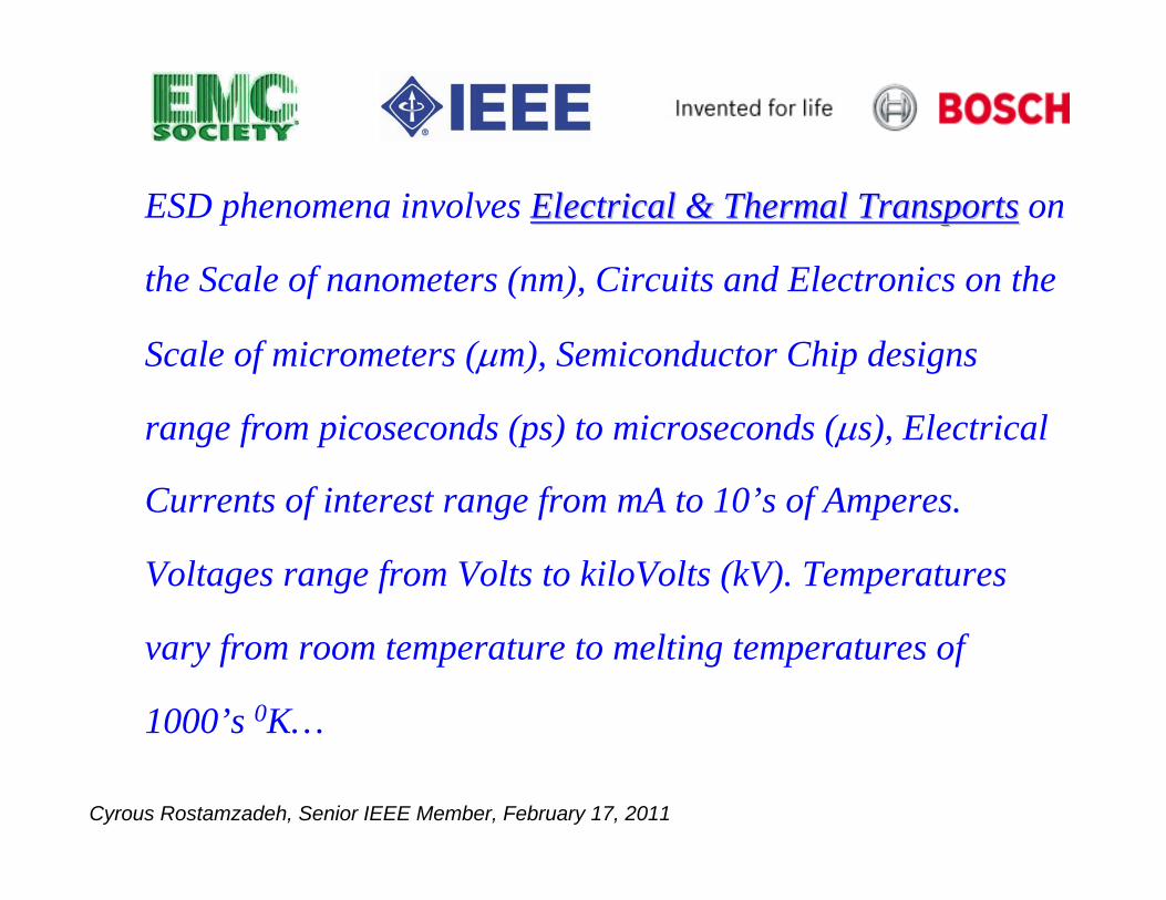
ESD phenomena involves Electrical & Thermal TransportsElectrical & Thermal Transports on
the Scale of nanometers (nm), Circuits and Electronics on the
Scale of micrometers (µm), Semiconductor Chip designs
range from picoseconds (ps) to microseconds (µs), Electrical
Currents of interest range from mA to 10’s of Amperes.
Voltages range from Volts to kiloVolts (kV). Temperatures
vary from room temperature to melting temperatures of
1000’s 0K…
Cyrous Rostamzadeh, Senior IEEE Member, February 17, 2011
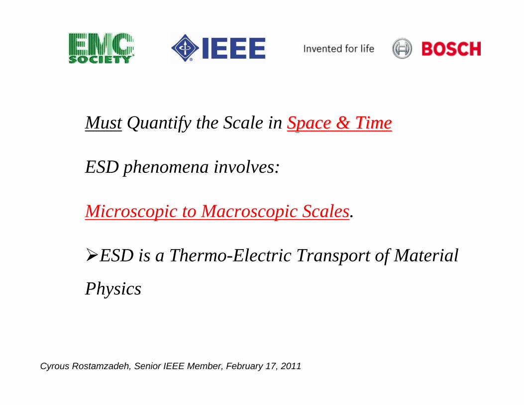
Must Quantify the Scale in Space & TimeSpace & Time
ESD phenomena involves:
Microscopic to Macroscopic Scales.
ESD is a Thermo-Electric Transport of Material
Physics

Cyrous Rostamzadeh, Senior IEEE Member, February 17, 2011
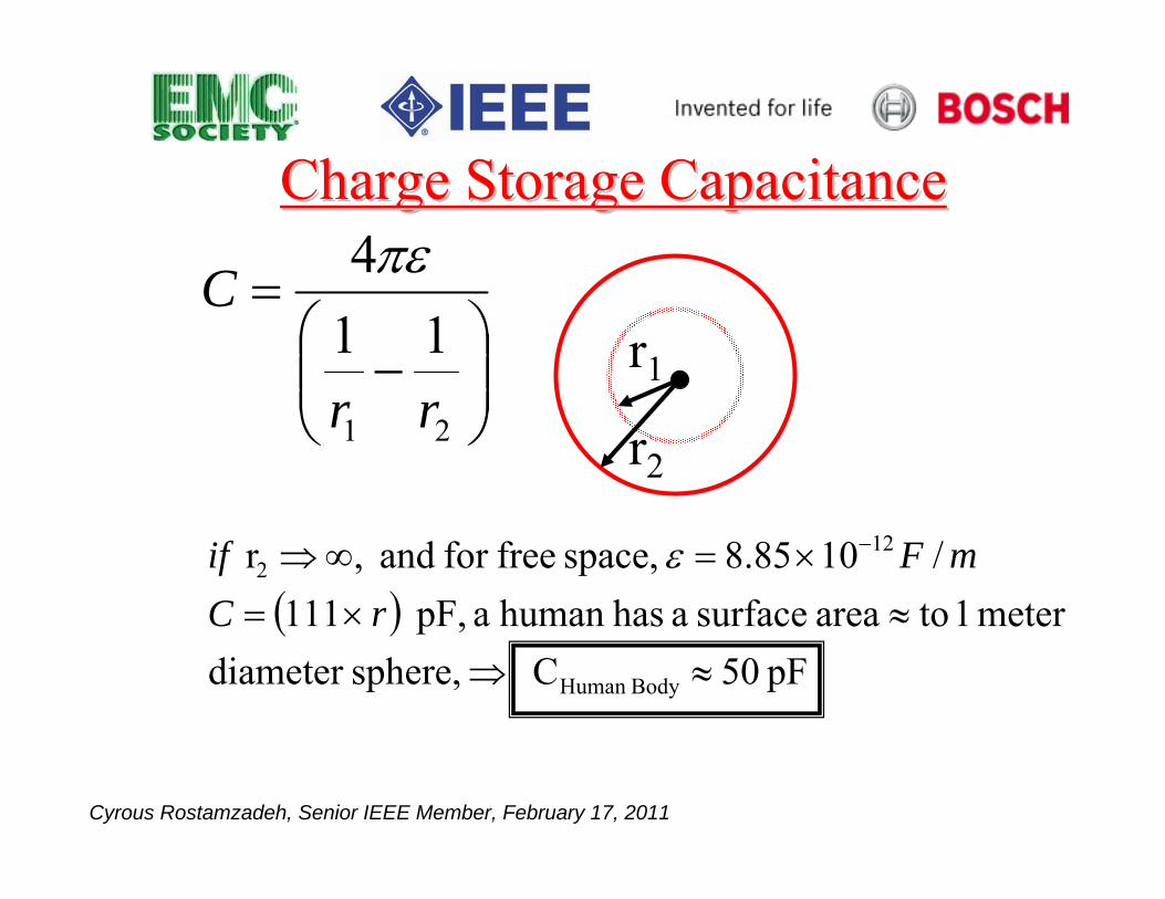
Capacitance – ESD Charge Storage Element
Cyrous Rostamzadeh, Senior IEEE Member, February 17, 2011
⎟⎟⎠
⎞⎜⎜⎝
⎛−
=
21
114
rr
C πε
r1
r2
( ) pF 50C sphere,diameter
meter 1 toarea surfacea has humana pF, 111/1085.8 space, freefor and ,r
BodyHuman
122
≈⇒≈×=
×=∞⇒ −
rCmFif ε
Charge Storage CapacitanceCharge Storage Capacitance
Cyrous Rostamzadeh, Senior IEEE Member, February 17, 2011
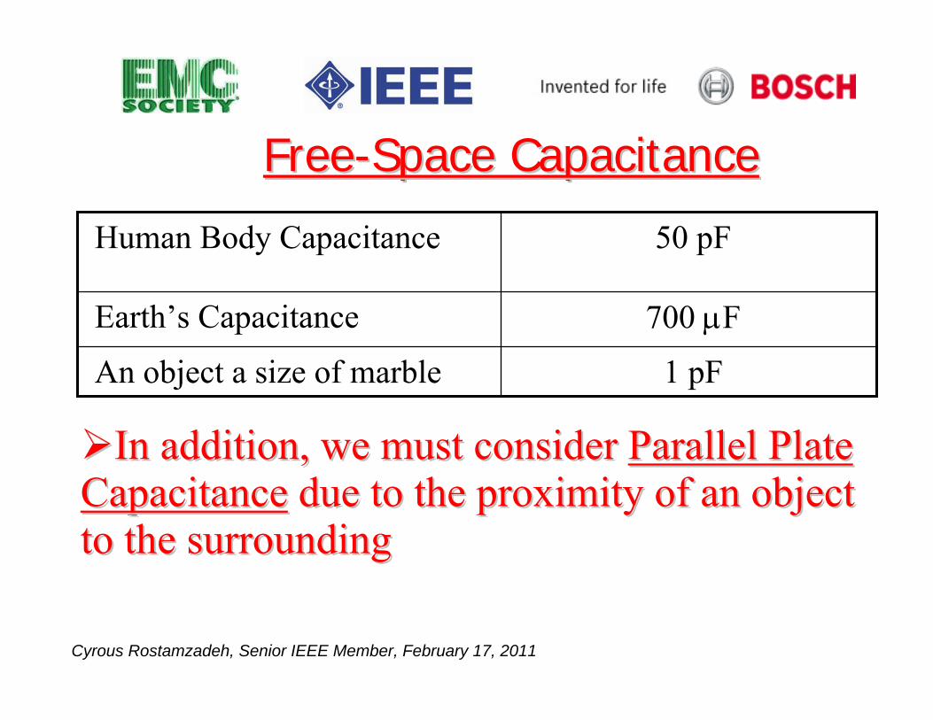
FreeFree--Space CapacitanceSpace Capacitance
1 pFAn object a size of marble
700 µFEarth’s Capacitance
50 pFHuman Body Capacitance
In addition, we must consider In addition, we must consider Parallel Plate Parallel Plate CapacitanceCapacitance due to the proximity of an object due to the proximity of an object to the surroundingto the surrounding

Cyrous Rostamzadeh, Senior IEEE Member, February 17, 2011
100 pF
50 pF to infinity
50 - 100 pF
500 Ω to 10 kΩ
Self-Capacitance
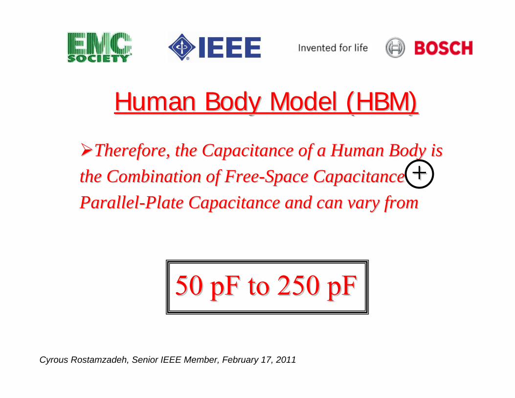
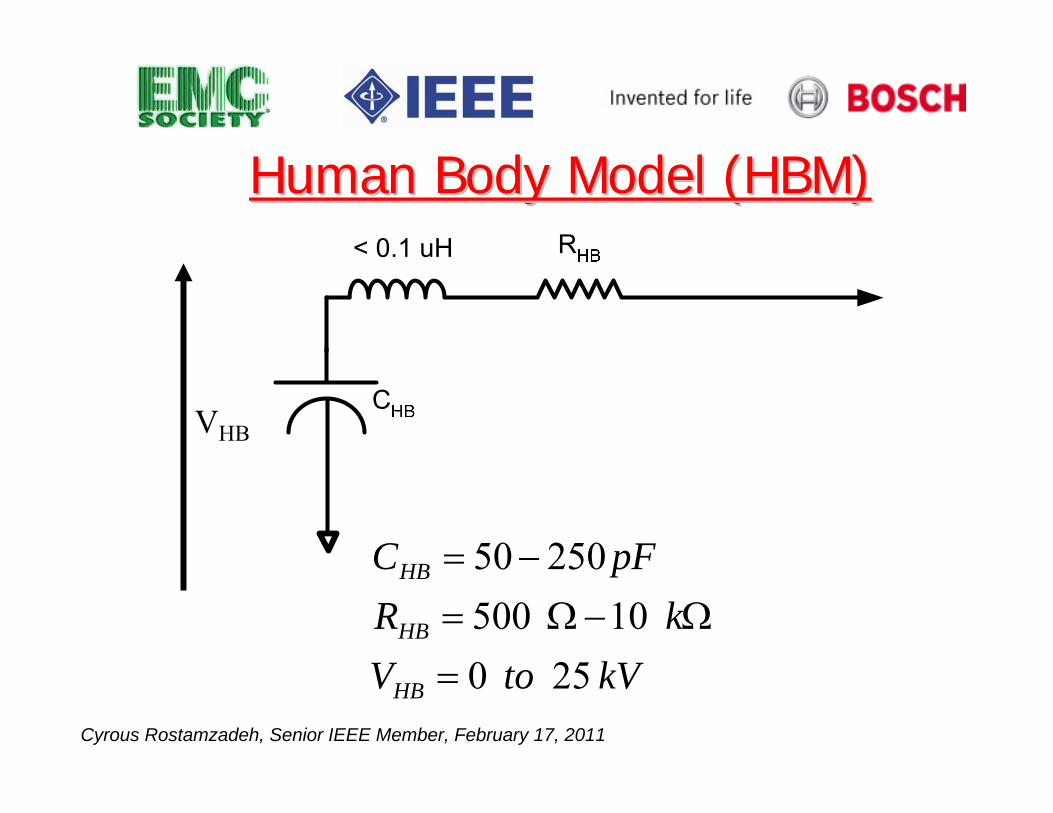
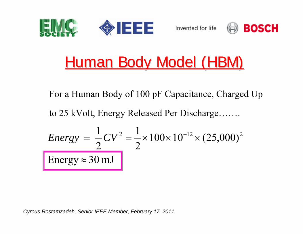
Human Body Model (HBM)Human Body Model (HBM)
Cyrous Rostamzadeh, Senior IEEE Member, February 17, 2011
Human Body Model (HBM)Human Body Model (HBM)
Therefore, the Capacitance of a Human Body is Therefore, the Capacitance of a Human Body is the Combination of Freethe Combination of Free--Space Capacitance Space Capacitance ++ParallelParallel--Plate Capacitance and can vary fromPlate Capacitance and can vary from
50 pF to 250 pF50 pF to 250 pF
Cyrous Rostamzadeh, Senior IEEE Member, February 17, 2011
kVtoVkR
pFC
HB
HB
HB
25 0 10 500
25050
=Ω−Ω=
−=
VHB
Human Body Model (HBM)Human Body Model (HBM)
Cyrous Rostamzadeh, Senior IEEE Member, February 17, 2011
mJ 30 Energy
)000,25(1010021
21 2122
≈
×××== −CVEnergy
For a Human Body of 100 pF Capacitance, Charged Up
to 25 kVolt, Energy Released Per Discharge…….
Human Body Model (HBM)Human Body Model (HBM)

Cyrous Rostamzadeh, Senior IEEE Member, February 17, 2011
The Discharge of a Human (via a small, hand-held metal piece) is basis for the current waveform most often used IEC 61000-4-2 standard.
Human Body Model (HBM)Human Body Model (HBM)

Cyrous Rostamzadeh, Senior IEEE Member, February 17, 2011
GM3097 (July 2006)
Ford EMC_CS_2009
Chrysler CS-11809ISO 10605 (2001) & IEC 61000ISO 10605 (2001) & IEC 61000--44--22 Standards with some Modifications.
Ambient Temperature: 23 +/- 3oC Relative Humidity 20 to 40% Prefer 20oC and 30% RH.Contact Rise Time: tr < 1 nsAir Discharge Rise Time: tr < 20 ns. Discharge Networks: 150 pF/2 kΩ and 330 pF/2 kΩ
OEM ESD Test SpecificationsOEM ESD Test Specifications

Cyrous Rostamzadeh, Senior IEEE Member, February 17, 2011
ESD Impact…
Cyrous Rostamzadeh, Senior IEEE Member, February 17, 2011
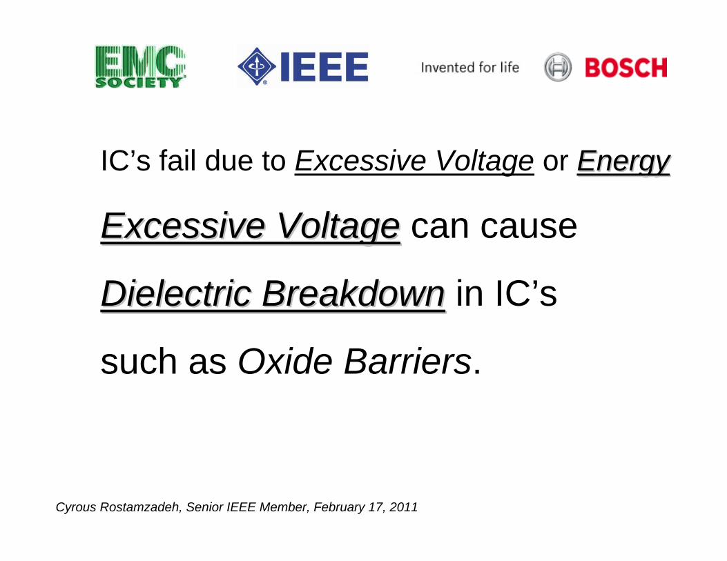
IC’s fail due to Excessive Voltage or EnergyEnergy
Excessive VoltageExcessive Voltage can cause
Dielectric BreakdownDielectric Breakdown in IC’s
such as Oxide Barriers.
Cyrous Rostamzadeh, Senior IEEE Member, February 17, 2011
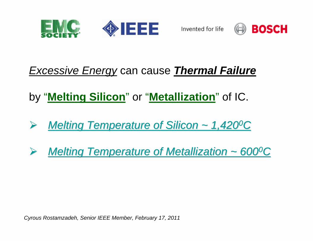
Excessive Energy can cause Thermal Failure
by “Melting Silicon” or “Metallization” of IC.
Melting Temperature of Silicon ~ 1,420Melting Temperature of Silicon ~ 1,42000CC
Melting Temperature of Metallization ~ 600Melting Temperature of Metallization ~ 60000CC
Cyrous Rostamzadeh, Senior IEEE Member, February 17, 2011
ESD Mathematical Analysis

Cyrous Rostamzadeh, Senior IEEE Member, February 17, 2011
⎟⎟⎠
⎞⎜⎜⎝
⎛ −•
⎟⎟⎠
⎞⎜⎜⎝
⎛+
⎟⎟⎠
⎞⎜⎜⎝
⎛
•+⎟⎟⎠
⎞⎜⎜⎝
⎛ −•
⎟⎟⎠
⎞⎜⎜⎝
⎛+
⎟⎟⎠
⎞⎜⎜⎝
⎛
•=4
3
3
2
2
2
1
1
1
1 exp
1
exp
1
)(τ
τ
ττ
τ
τ t
t
t
kit
t
t
kiti n
n
n
n
, exp/1
1
2
2
11 ⎟
⎟
⎠
⎞
⎜⎜
⎝
⎛⎟⎟⎠
⎞⎜⎜⎝
⎛−=
nnkττ
ττ
⎟⎟
⎠
⎞
⎜⎜
⎝
⎛⎟⎟⎠
⎞⎜⎜⎝
⎛−=
nnk
/1
3
4
4
32 exp
ττ
ττ
τ4 = 58 nsτ2 = 1.7 nsI2 = 10.1 Ampn = 3τ3 = 6 nsτ1 = 1.3 nsI1 = 21.9 Amp
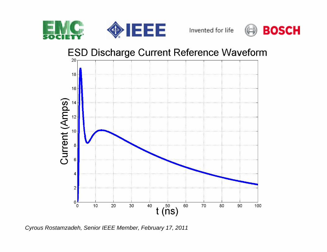
Cyrous Rostamzadeh, Senior IEEE Member, February 17, 2011
Cyrous Rostamzadeh, Senior IEEE Member, February 17, 2011
Cyrous Rostamzadeh, Senior IEEE Member, February 17, 2011
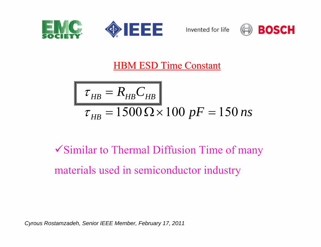
HBM ESD Time ConstantHBM ESD Time Constant
nspFCR
HB
HBHBHB
150 100 1500 =×Ω==
ττ
Similar to Thermal Diffusion Time of many
materials used in semiconductor industry

Cyrous Rostamzadeh, Senior IEEE Member, February 17, 2011
ESD is a Non-Linear Electro-Thermal Physical Event.
Very Difficult to Model Accurately.
Simple Linear Model is insightful.
Cyrous Rostamzadeh, Senior IEEE Member, February 17, 2011
ESD Modeling…
Cyrous Rostamzadeh, Senior IEEE Member, February 17, 2011
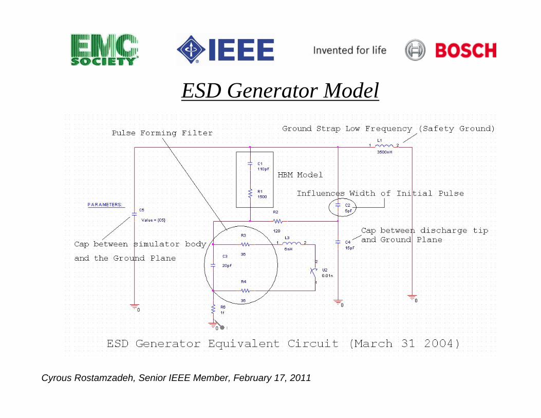
ESD Generator Model

Cyrous Rostamzadeh, Senior IEEE Member, February 17, 2011
VGen = 8 kVESD Generator Model

Cyrous Rostamzadeh, Senior IEEE Member, February 17, 2011
VHBM = 25 kVESD HBM Model
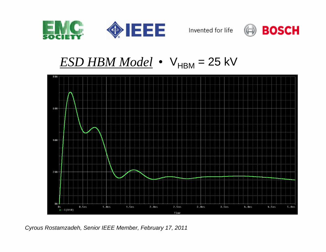
Cyrous Rostamzadeh, Senior IEEE Member, February 17, 2011
• VHBM = 25 kVESD HBM Model

Cyrous Rostamzadeh, Senior IEEE Member, February 17, 2011
ESD Protection Schemes
Cyrous Rostamzadeh, Senior IEEE Member, February 17, 2011
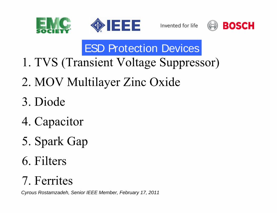
ESD Protection Devices1. TVS (Transient Voltage Suppressor)2. MOV Multilayer Zinc Oxide3. Diode4. Capacitor5. Spark Gap6. Filters7. Ferrites
Cyrous Rostamzadeh, Senior IEEE Member, February 17, 2011
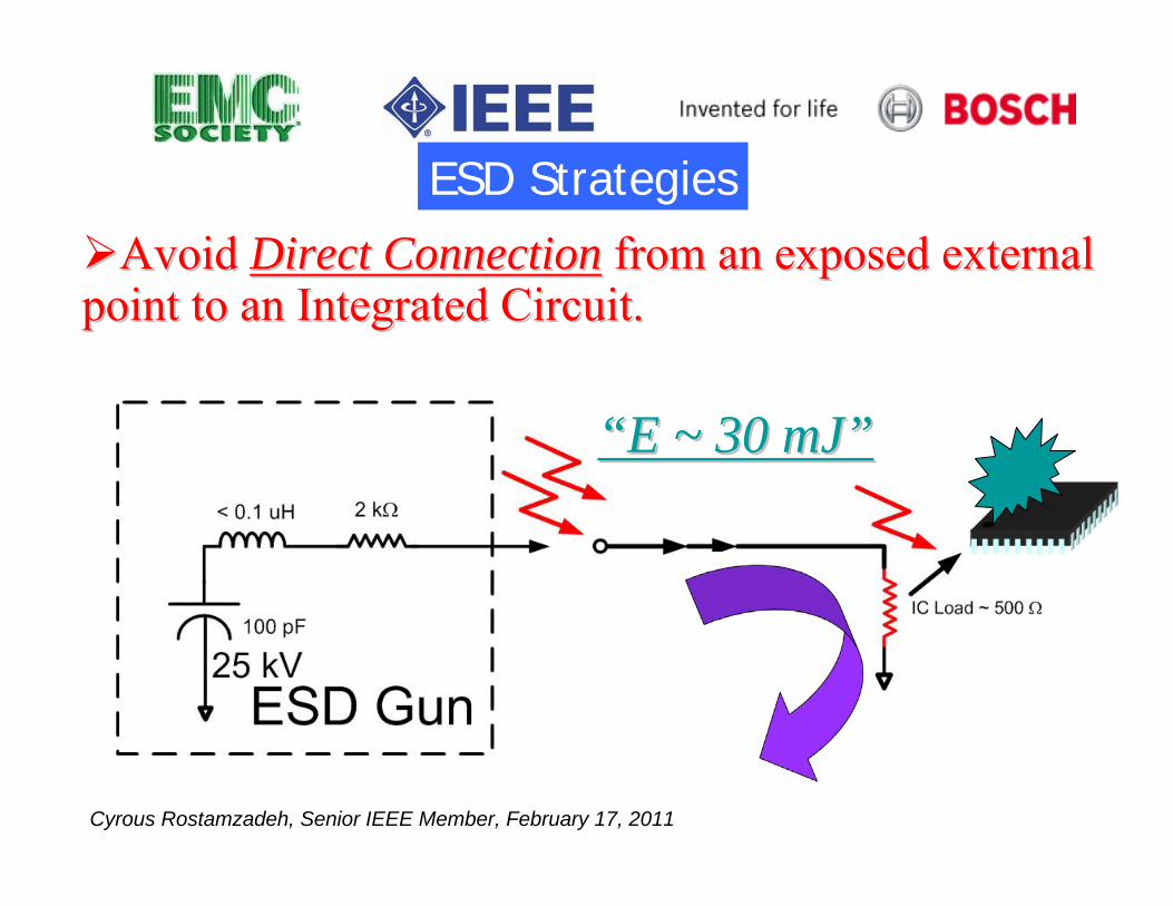
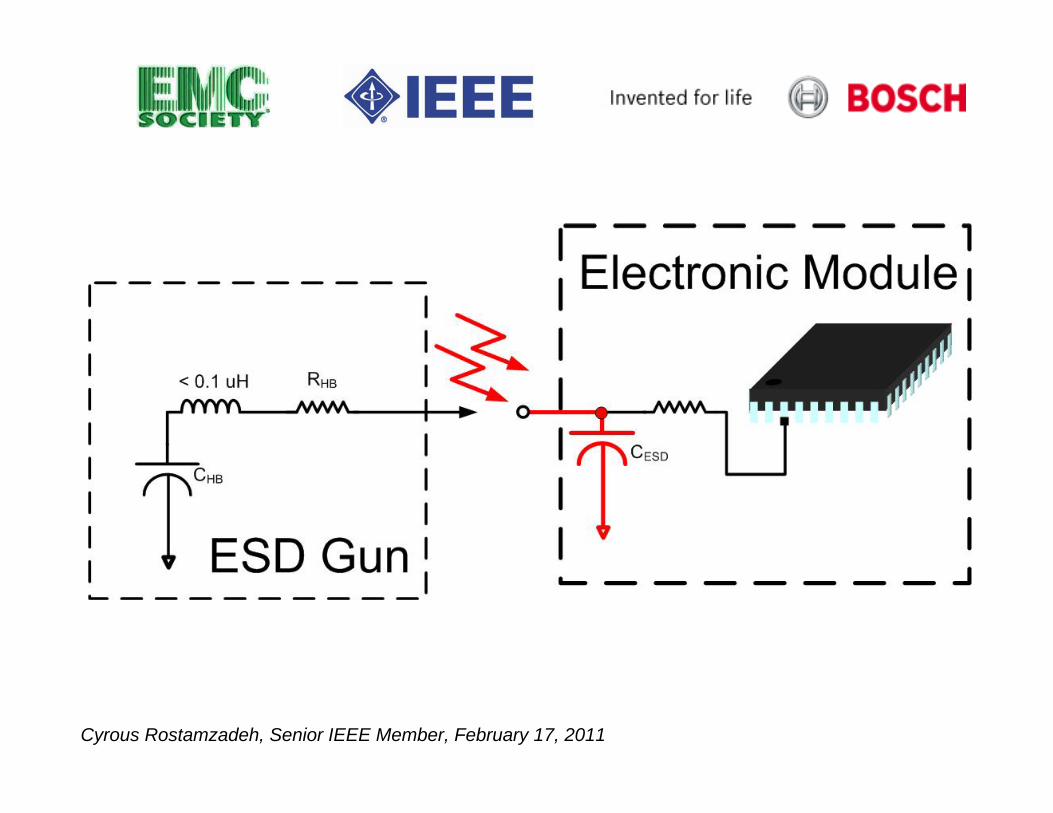
Avoid Avoid Direct ConnectionDirect Connection from an exposed external from an exposed external point to an Integrated Circuit.point to an Integrated Circuit.
ESD Strategies
““E ~ 30 mJE ~ 30 mJ””

Cyrous Rostamzadeh, Senior IEEE Member, February 17, 2011
ESD Strategies
In no case should there be a directIn no case should there be a direct
connection from an Integrated Circuitconnection from an Integrated Circuit
to an exposed external point.to an exposed external point.

Cyrous Rostamzadeh, Senior IEEE Member, February 17, 2011
ESD Strategies
Divert or limit the ESD Energy awayDivert or limit the ESD Energy away
from Circuit Inputs using Filters orfrom Circuit Inputs using Filters or
Transient Suppressors.Transient Suppressors.
Cyrous Rostamzadeh, Senior IEEE Member, February 17, 2011
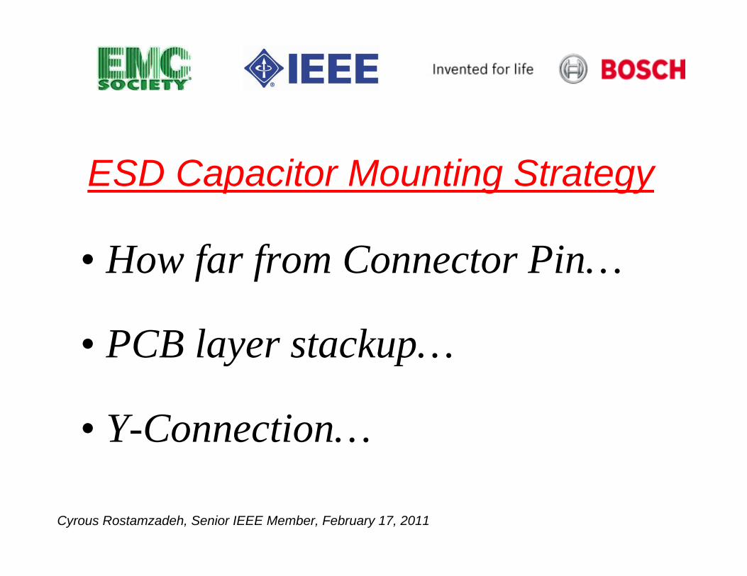
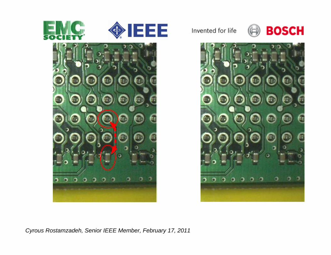
ESD Capacitor Mounting Strategy
• How far from Connector Pin…
• PCB layer stackup…
• Y-Connection…

Cyrous Rostamzadeh, Senior IEEE Member, February 17, 2011
ESD Capacitor Failure Mode
Voltage – Pressure
Current – Force
Dielectric Breakdown
Cyrous Rostamzadeh, Senior IEEE Member, February 17, 2011
Cyrous Rostamzadeh, Senior IEEE Member, February 17, 2011
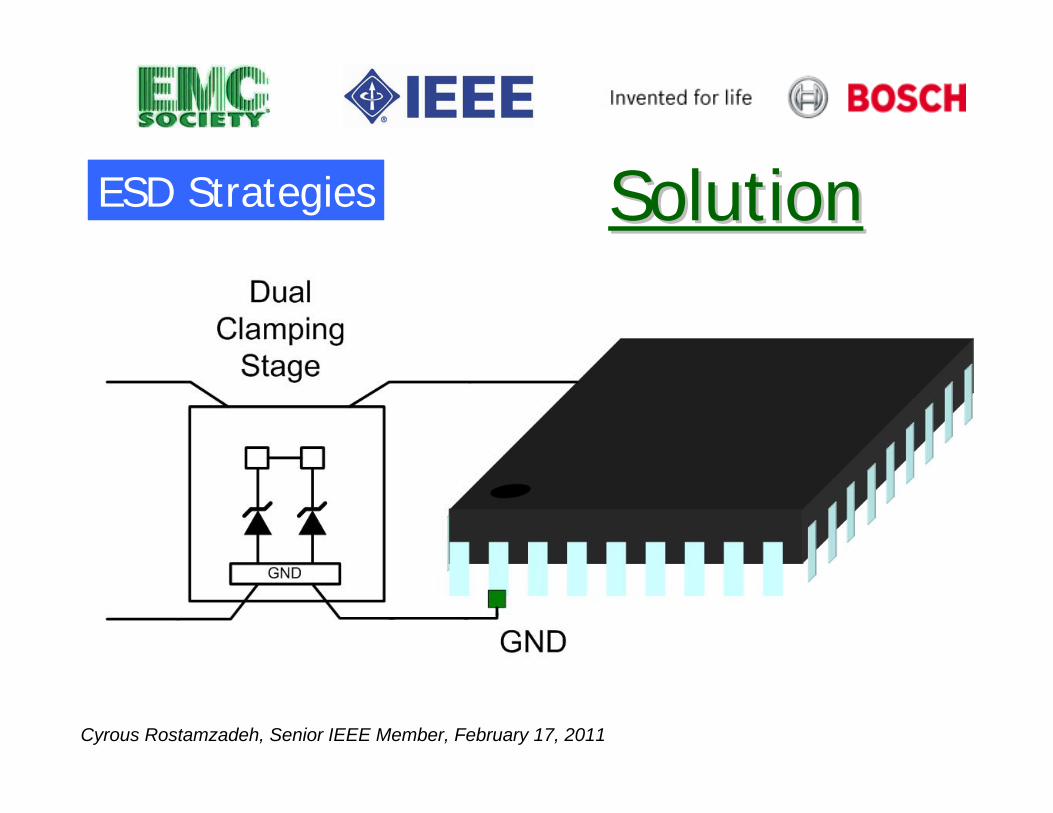
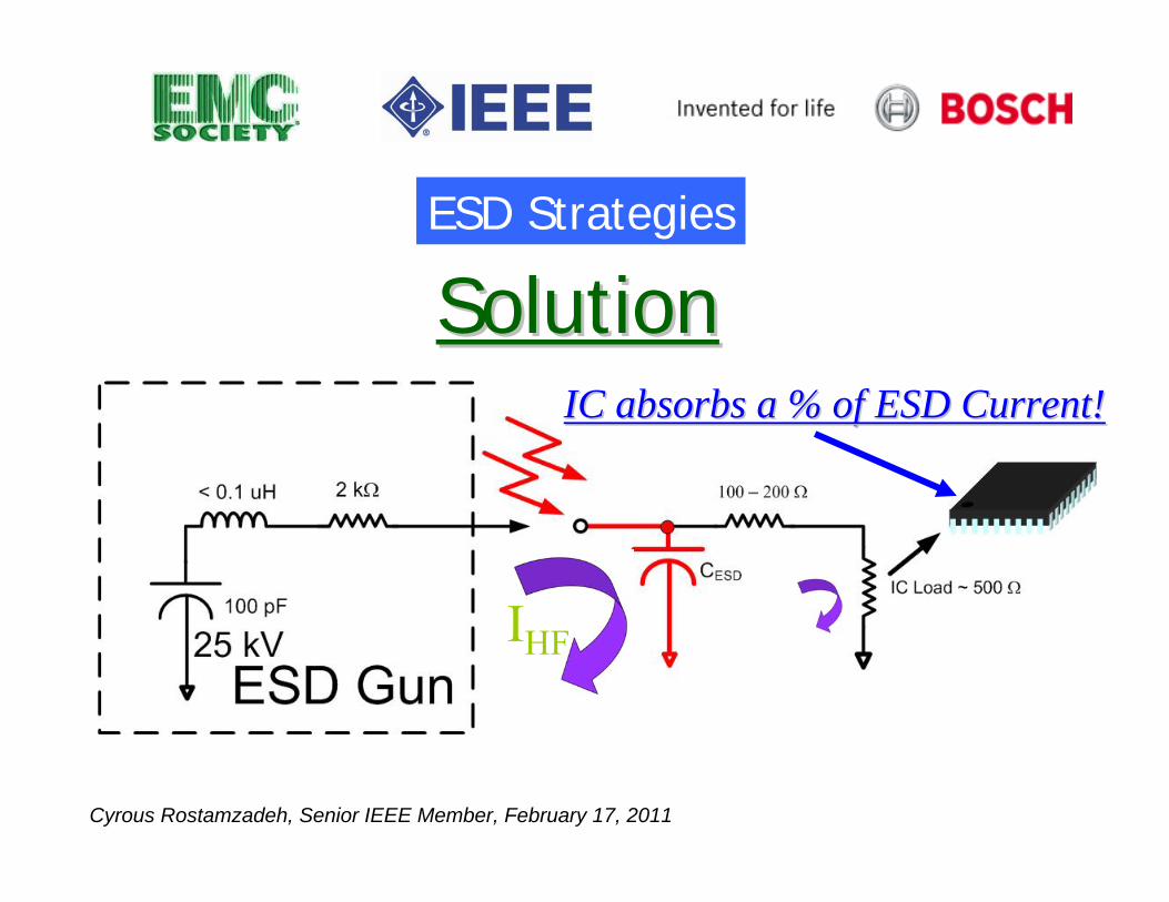
SolutionSolutionESD Strategies
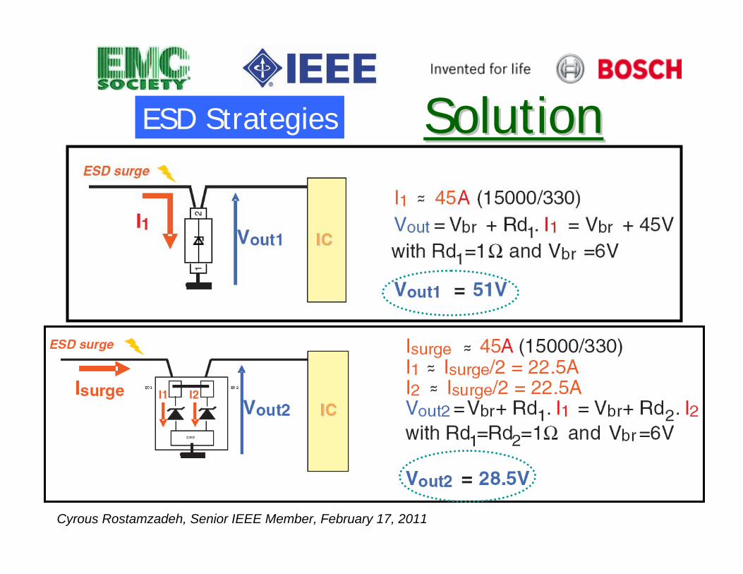
Cyrous Rostamzadeh, Senior IEEE Member, February 17, 2011
ESD Strategies SolutionSolution

Cyrous Rostamzadeh, Senior IEEE Member, February 17, 2011
SolutionSolutionESD Strategies

Cyrous Rostamzadeh, Senior IEEE Member, February 17, 2011
Use LOW Capacitance Protection
ESD Strategies
Cyrous Rostamzadeh, Senior IEEE Member, February 17, 2011
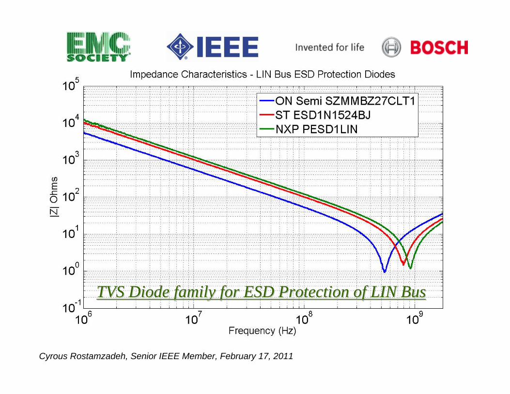
TVS Diode family for ESD Protection of LIN BusTVS Diode family for ESD Protection of LIN Bus

Cyrous Rostamzadeh, Senior IEEE Member, February 17, 2011
TVS Diode Bias ImpactTVS Diode Bias Impact
Cyrous Rostamzadeh, Senior IEEE Member, February 17, 2011
IHF
SolutionSolutionESD Strategies
IC absorbs a % of ESD Current!IC absorbs a % of ESD Current!
Cyrous Rostamzadeh, Senior IEEE Member, February 17, 2011
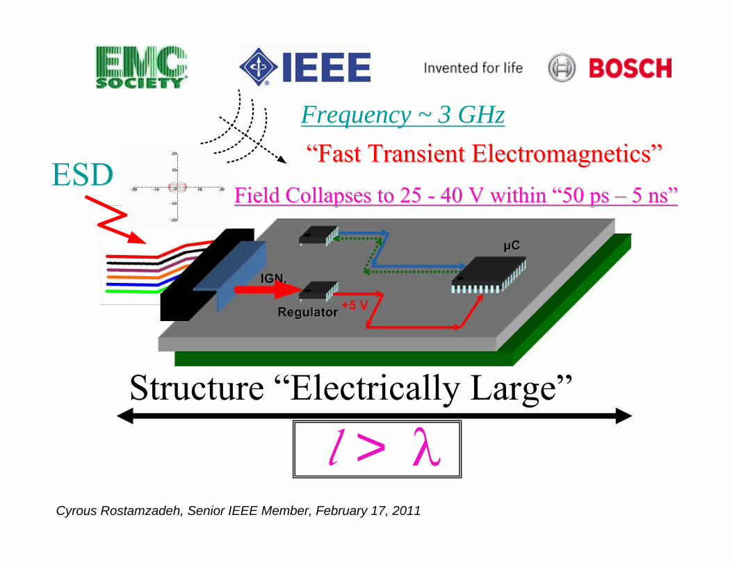
l > λ
ESD““Fast Transient ElectromagneticsFast Transient Electromagnetics””
Structure “Electrically Large”
Frequency ~ 3 GHz
Field Collapses to 25 Field Collapses to 25 -- 40 V within 40 V within ““50 ps 50 ps –– 5 ns5 ns””

Cyrous Rostamzadeh, Senior IEEE Member, February 17, 2011
High Frequency Design Practice ESD
Cyrous Rostamzadeh, Senior IEEE Member, February 17, 2011
Spark Gap “Protection Mechanism”

Cyrous Rostamzadeh, Senior IEEE Member, February 17, 2011
Spark Gap
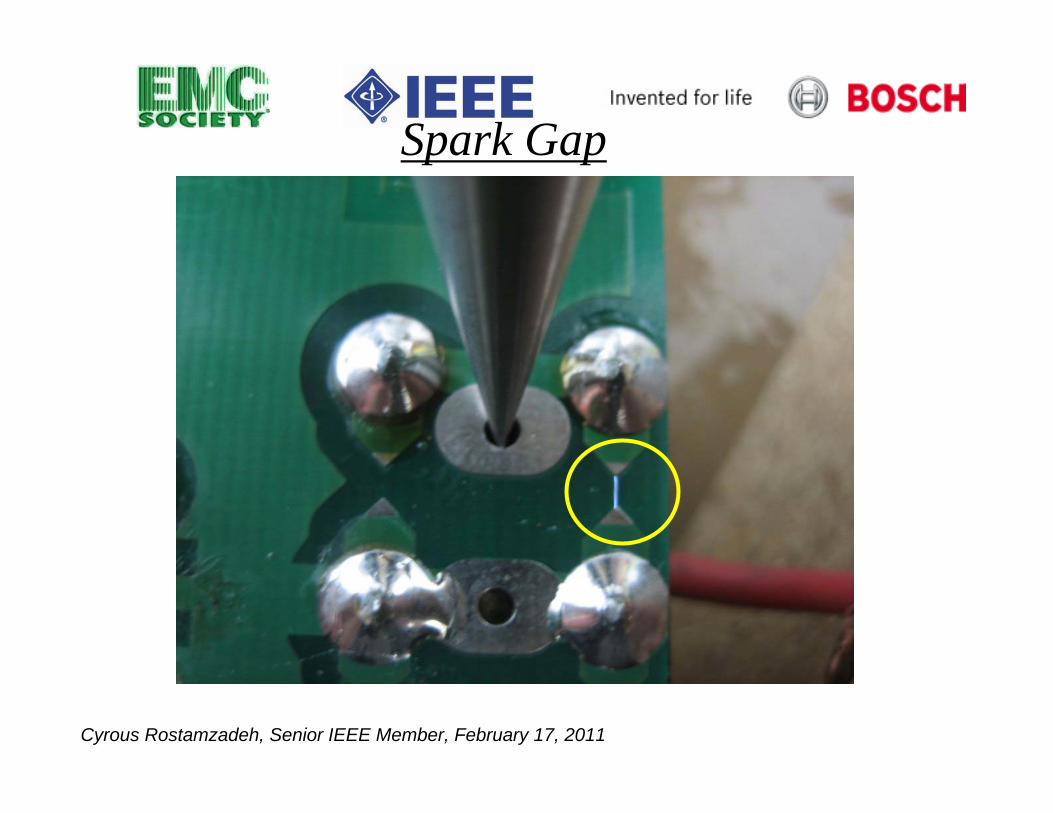
Cyrous Rostamzadeh, Senior IEEE Member, February 17, 2011
Spark Gap
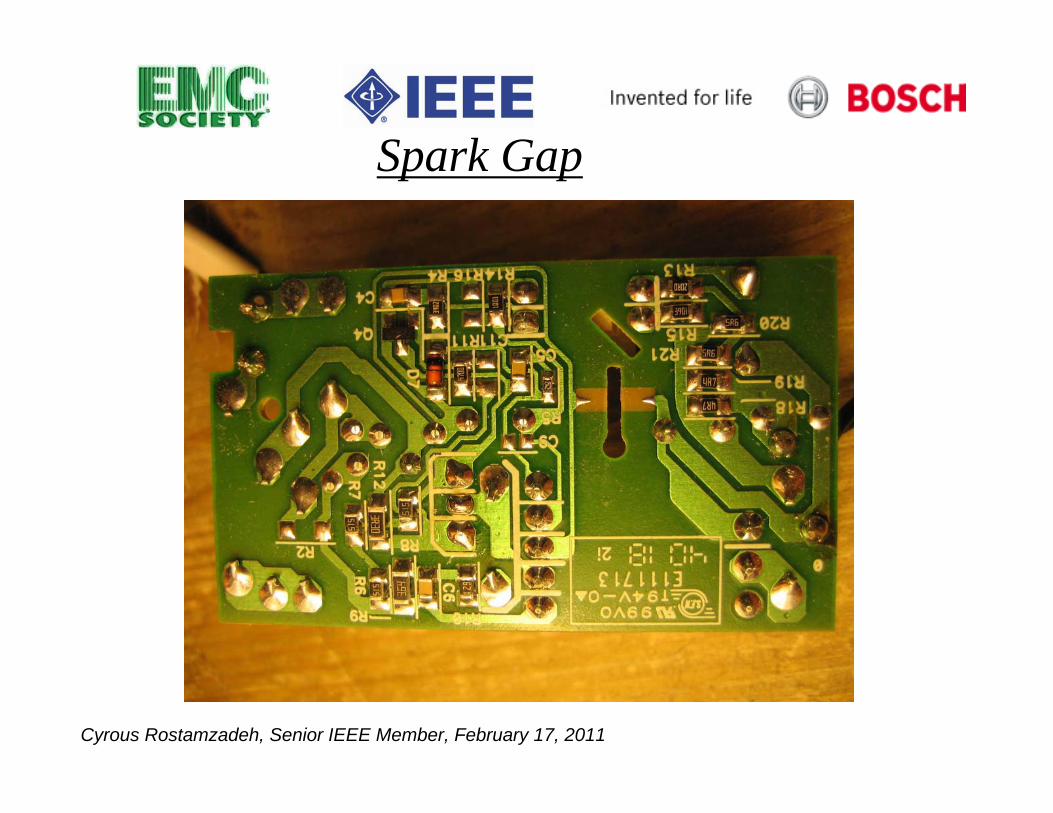
Cyrous Rostamzadeh, Senior IEEE Member, February 17, 2011
Spark Gap
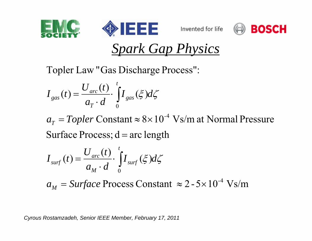
Cyrous Rostamzadeh, Senior IEEE Member, February 17, 2011
Vs/m 105-2 Constant Process
)()()(
length arc d Process; SurfacePressure Normalat Vs/m 108 Constant
)()()(
:Process" Discharge Gas" LawTopler
4-0
4-0
×≈=
⋅⋅
=
=×≈=
⋅⋅
=
∫
∫
Surfacea
dIdatUtI
Toplera
dIdatUtI
M
t
surfM
arcsurf
T
t
gasT
arcgas
ζξ
ζξ
Spark Gap Physics
Cyrous Rostamzadeh, Senior IEEE Member, February 17, 2011
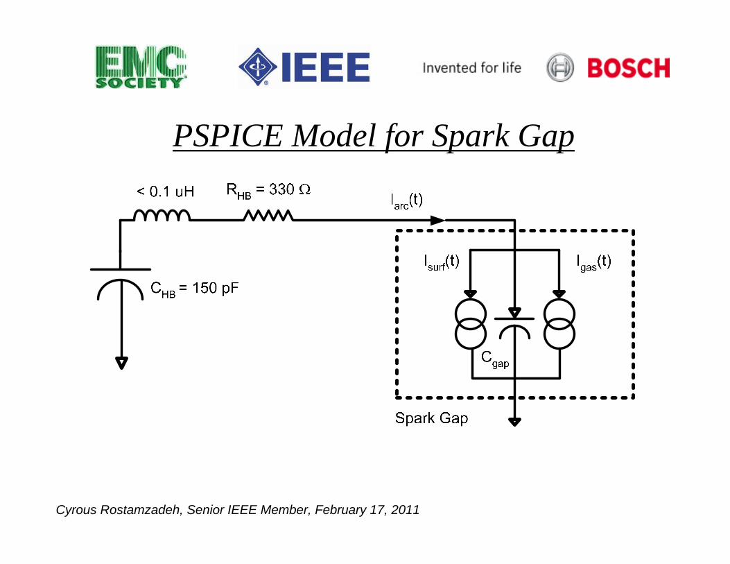
PSPICE Model for Spark Gap

Cyrous Rostamzadeh, Senior IEEE Member, February 17, 2011
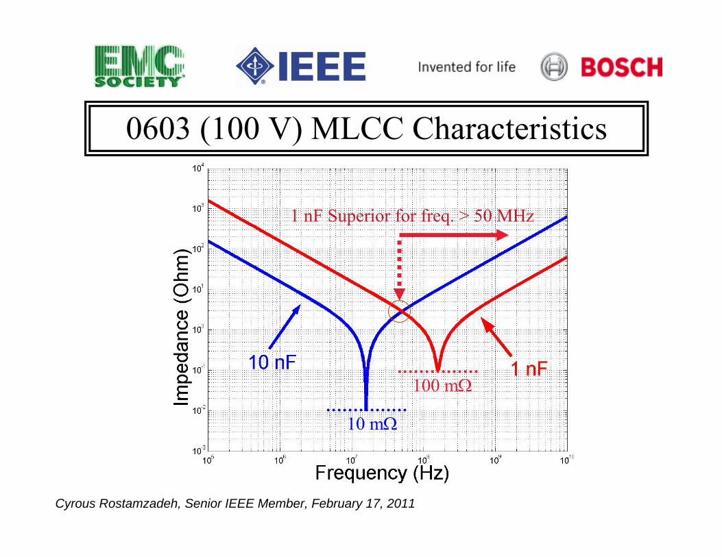
0201 0402 0603 0805 1206 1210 1812 1825 2220 2225
MLCC Package SizeMLCC Package Size
Cyrous Rostamzadeh, Senior IEEE Member, February 17, 2011
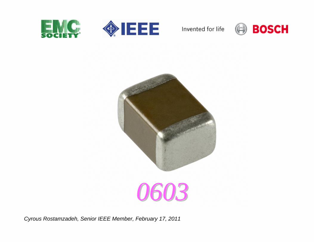
06030603

Cyrous Rostamzadeh, Senior IEEE Member, February 17, 2011
ESD Capacitors ESD Capacitors –– Mounting StrategyMounting Strategy

Cyrous Rostamzadeh, Senior IEEE Member, February 17, 2011
Strategic Insertion Topology of MLCC ConceptStrategic Insertion Topology of MLCC Concept……
MurataMurataTDKTDK
EPCOSEPCOS

Cyrous Rostamzadeh, Senior IEEE Member, February 17, 2011
FlashFlash
µµCC
RegulatorRegulator
IGN.IGN.
+5 V+5 V
ESD Capacitors – Mounting Strategy

Cyrous Rostamzadeh, Senior IEEE Member, February 17, 2011
TVS Diode Mounting Strategy

Cyrous Rostamzadeh, Senior IEEE Member, February 17, 2011
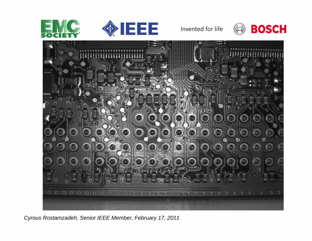
ESD Capacitors Mounted @ PCB Connector Pins

Cyrous Rostamzadeh, Senior IEEE Member, February 17, 2011
ESD Event (High Frequency Current through ESD MLCC)
PCB Mounted MLCC Exposed to HBM ESD
Cyrous Rostamzadeh, Senior IEEE Member, February 17, 2011
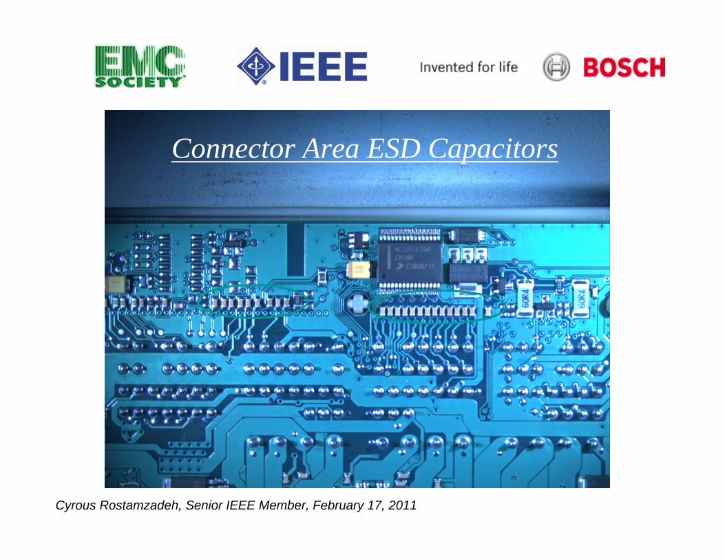
Connector Area ESD Capacitors

Cyrous Rostamzadeh, Senior IEEE Member, February 17, 2011
Connector Area ESD Capacitors
Cyrous Rostamzadeh, Senior IEEE Member, February 17, 2011
Cyrous Rostamzadeh, Senior IEEE Member, February 17, 2011
Cyrous Rostamzadeh, Senior IEEE Member, February 17, 2011
Electrical Characteristics

Cyrous Rostamzadeh, Senior IEEE Member, February 17, 2011
180 pF/50V, C0G – X7R

Cyrous Rostamzadeh, Senior IEEE Member, February 17, 2011
1 nF/50 V, C0G – X7R

Cyrous Rostamzadeh, Senior IEEE Member, February 17, 2011
X7R
Cyrous Rostamzadeh, Senior IEEE Member, February 17, 2011
ESR - function of Frequency
Cyrous Rostamzadeh, Senior IEEE Member, February 17, 2011
MLCC Supported via 2 cm2 cm Long Wires Exposed to HBM ESD

Cyrous Rostamzadeh, Senior IEEE Member, February 17, 2011
MLCC GeometriesMLCC Geometries
2.ESD Enhanced
1.Standard MLCCplates do notoverlap over
indicated regions

Cyrous Rostamzadeh, Senior IEEE Member, February 17, 2011
When not intersecting When intersecting
The Electric Flux Density is higher on the terminal electrode edge.
Cyrous Rostamzadeh, Senior IEEE Member, February 17, 2011
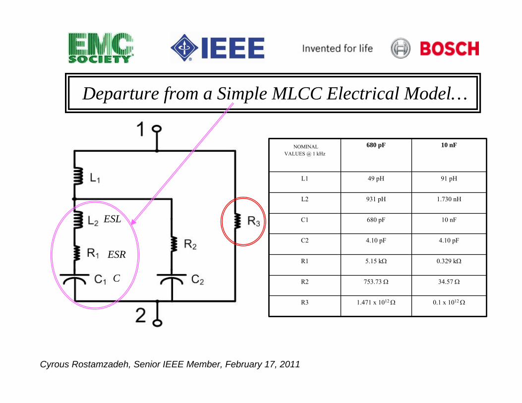
Departure from a Simple MLCC Electrical Model…
0.1 x 10¹² Ω1.471 x 10¹² ΩR3
34.57 Ω753.73 ΩR2
0.329 kΩ5.15 kΩR1
4.10 pF4.10 pFC2
10 nF680 pFC1
1.730 nH931 pHL2
91 pH49 pHL1
10 nF680 pFNOMINALVALUES @ 1 kHz
C
ESR
ESL
Cyrous Rostamzadeh, Senior IEEE Member, February 17, 2011
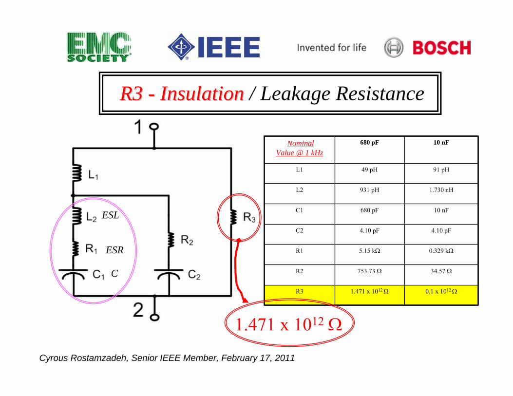
R3 R3 -- InsulationInsulation / Leakage Resistance
0.1 x 10¹² Ω1.471 x 10¹² ΩR3
34.57 Ω753.73 ΩR2
0.329 kΩ5.15 kΩR1
4.10 pF4.10 pFC2
10 nF680 pFC1
1.730 nH931 pHL2
91 pH49 pHL1
10 nF680 pFNominalValue @ 1 kHz
C
ESR
ESL
1.471 x 10¹² Ω
Cyrous Rostamzadeh, Senior IEEE Member, February 17, 2011
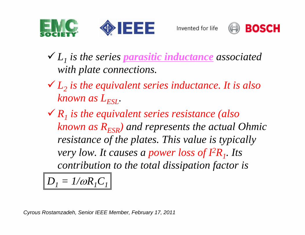
L1 is the series parasitic inductance associated with plate connections.L2 is the equivalent series inductance. It is also known as LESL. R1 is the equivalent series resistance (also known as RESR) and represents the actual Ohmic resistance of the plates. This value is typically very low. It causes a power loss of I2R1. Its contribution to the total dissipation factor is
D1 = 1/ωR1C1
Cyrous Rostamzadeh, Senior IEEE Member, February 17, 2011
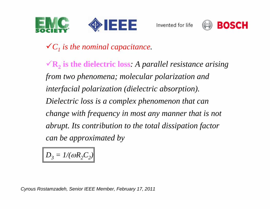
C1 is the nominal capacitance.
R2 is the dielectric loss: A parallel resistance arising from two phenomena; molecular polarization and interfacial polarization (dielectric absorption). Dielectric loss is a complex phenomenon that can change with frequency in most any manner that is not abrupt. Its contribution to the total dissipation factor can be approximated by
D3 = 1/(ωR2C2)

Cyrous Rostamzadeh, Senior IEEE Member, February 17, 2011
C2 is the parallel dielectric absorption capacitor.R3 is the leakage resistance, or insulation resistance: A parallel resistance due to leakage current in the capacitor. This value is typically very high. It causes a power loss of V2/R3. Its contribution to the total dissipation factor is
D2 = 1/(ωR3C1)

Cyrous Rostamzadeh, Senior IEEE Member, February 17, 2011
Z
ESR
10nF/50V – X7R

Cyrous Rostamzadeh, Senior IEEE Member, February 17, 2011
ESR
Z 680pF/50V – X7R

Cyrous Rostamzadeh, Senior IEEE Member, February 17, 2011
MLCC Pre-ESD & Post ESD
ImpedanceCharacterization

Cyrous Rostamzadeh, Senior IEEE Member, February 17, 2011
Pre-ESD

Cyrous Rostamzadeh, Senior IEEE Member, February 17, 2011
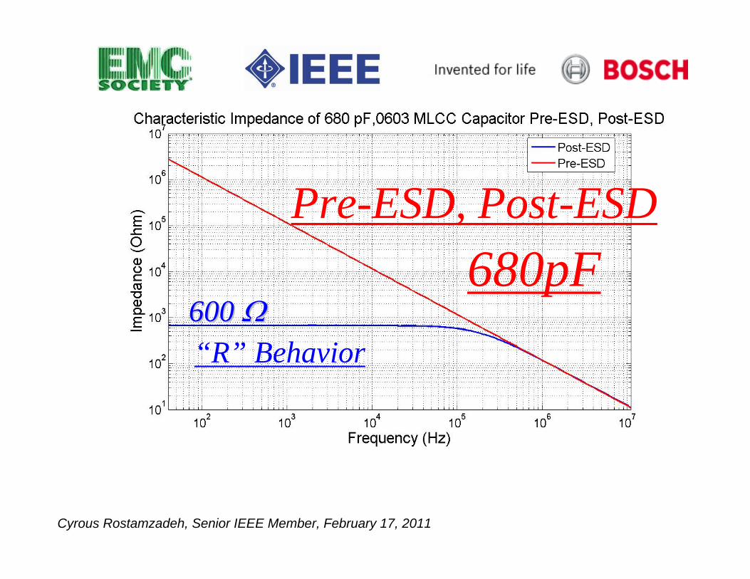
Pre-ESD, Post-ESD
“R” Behavior
10nF
Cyrous Rostamzadeh, Senior IEEE Member, February 17, 2011
“R” Behavior
Pre-ESD, Post-ESD680pF
600 600 ΩΩ

Cyrous Rostamzadeh, Senior IEEE Member, February 17, 2011
Post-ESD680pF, 10nF
Cyrous Rostamzadeh, Senior IEEE Member, February 17, 2011
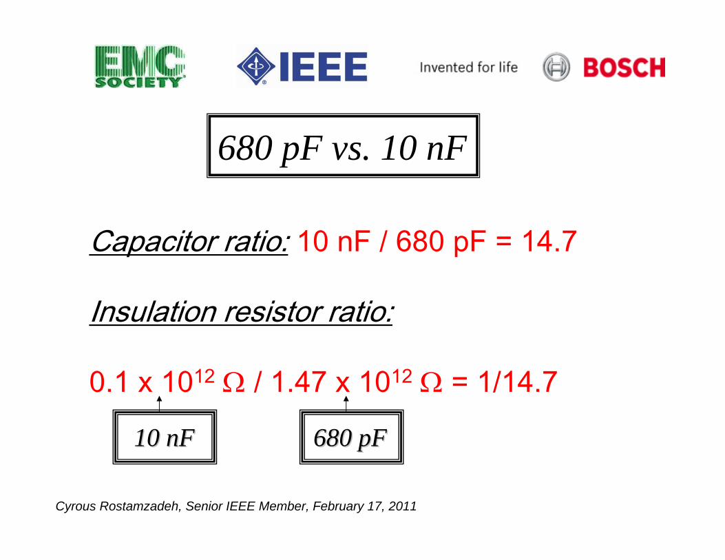
Capacitor ratio: 10 nF / 680 pF = 14.7
Insulation resistor ratio:
0.1 x 10¹² Ω / 1.47 x 10¹² Ω = 1/14.7
680 pF vs. 10 nF
10 10 nFnF 680 pF680 pF
Cyrous Rostamzadeh, Senior IEEE Member, February 17, 2011
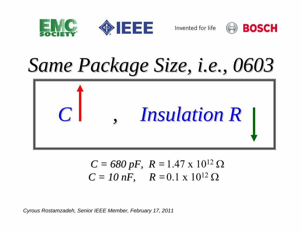
Same Package Size, i.e., 0603Same Package Size, i.e., 0603
CC , , Insulation RInsulation R
C = 680 pF, R = C = 680 pF, R = 1.47 x 10¹² ΩC = 10 C = 10 nFnF, R = , R = 0.1 x 10¹² Ω

Cyrous Rostamzadeh, Senior IEEE Member, February 17, 2011
Post-ESD, R3 - Leakage Resistance ‘Degradation’
13
31
21~
|| :
CRf
RCsFrequencielowAt
π
Pre-ESD: C1 = 680 pF, R3 = 1.471 x 10¹² ΩPost-ESD: C1 = 680 pF, R3 = 500 Ω (40 Hz – 200 kHz)Pre-ESD: C1 = 10 nF, R3 = 0.1 x 10¹² ΩPost-ESD: C1 = 10 nF, R3 = 500 Ω (40 Hz – 20 kHz)

Cyrous Rostamzadeh, Senior IEEE Member, February 17, 2011
Post-ESD5.7nF, 0805

Cyrous Rostamzadeh, Senior IEEE Member, February 17, 2011
ESD ImpactESD Impact
Cyrous Rostamzadeh, Senior IEEE Member, February 17, 2011
MLCC Post ESD Optical Imaging
Cyrous Rostamzadeh, Senior IEEE Member, February 17, 2011
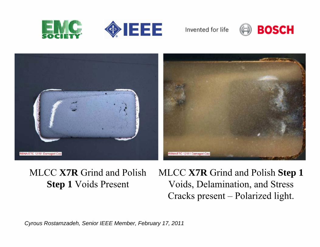
MLCC X7R Grind and PolishStep 1 Voids Present
MLCC X7R Grind and Polish Step 1Voids, Delamination, and StressCracks present – Polarized light.
Cyrous Rostamzadeh, Senior IEEE Member, February 17, 2011
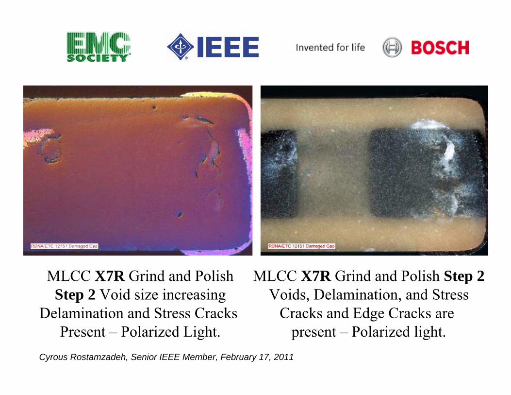
MLCC X7R Grind and PolishStep 2 Void size increasing
Delamination and Stress Cracks Present – Polarized Light.
MLCC X7R Grind and Polish Step 2Voids, Delamination, and Stress
Cracks and Edge Cracks are present – Polarized light.
Cyrous Rostamzadeh, Senior IEEE Member, February 17, 2011
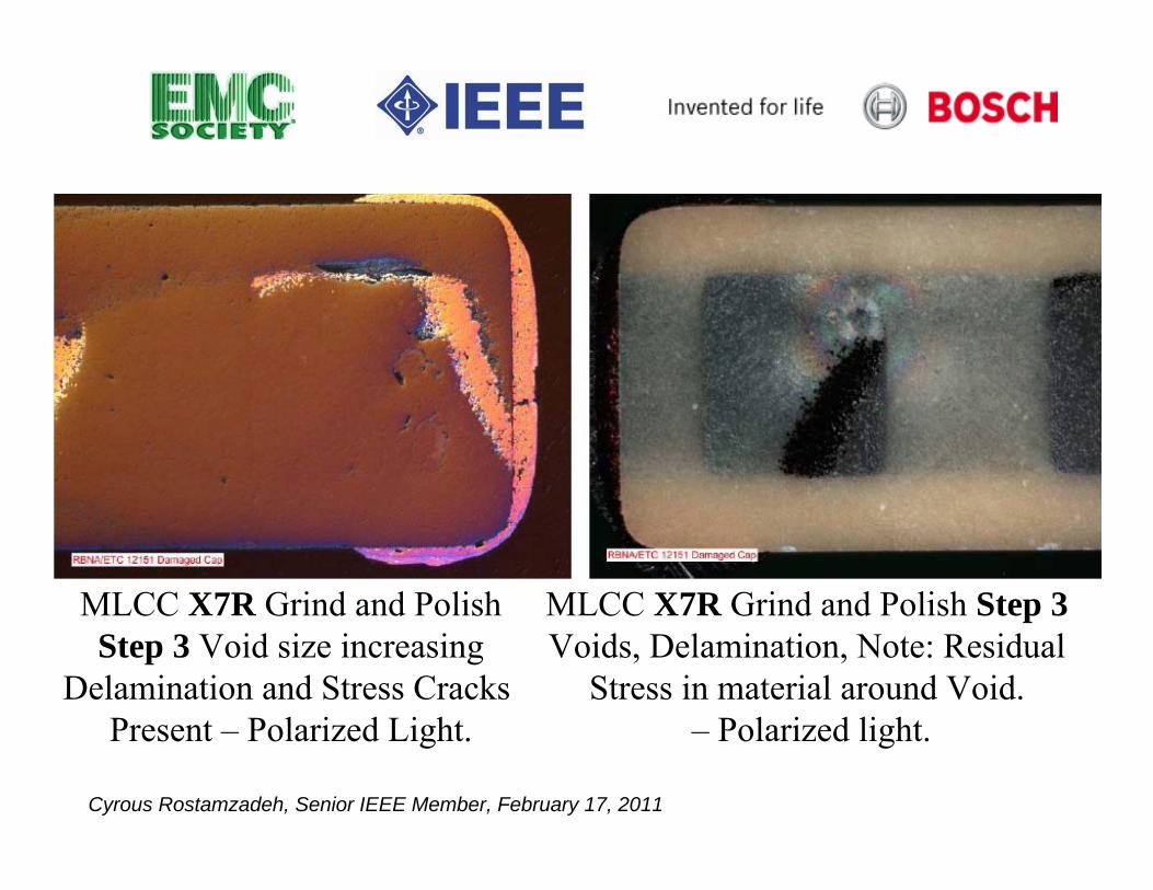
MLCC X7R Grind and PolishStep 3 Void size increasing
Delamination and Stress Cracks Present – Polarized Light.
MLCC X7R Grind and Polish Step 3Voids, Delamination, Note: Residual
Stress in material around Void.– Polarized light.

Cyrous Rostamzadeh, Senior IEEE Member, February 17, 2011
MLCC X7R Grind and PolishStep 4 Void size increasing
Delamination - Polarized Light.
MLCC X7R Grind and Polish Step 4Voids, Delamination, and Stress Cracks present – Polarized light.
Cyrous Rostamzadeh, Senior IEEE Member, February 17, 2011
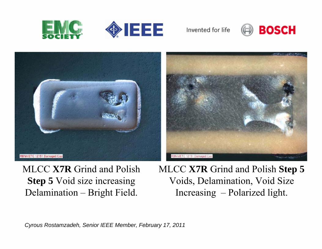
MLCC X7R Grind and PolishStep 5 Void size increasingDelamination – Bright Field.
MLCC X7R Grind and Polish Step 5Voids, Delamination, Void Size
Increasing – Polarized light.

Cyrous Rostamzadeh, Senior IEEE Member, February 17, 2011
MLCC X7R Bubble Discovered end cap

Cyrous Rostamzadeh, Senior IEEE Member, February 17, 2011
MLCC C0G Void / Micro Cracks MLCC C0G Void / Micro CracksPolarized DIC

Cyrous Rostamzadeh, Senior IEEE Member, February 17, 2011

Cyrous Rostamzadeh, Senior IEEE Member, February 17, 2011

Cyrous Rostamzadeh, Senior IEEE Member, February 17, 2011

Cyrous Rostamzadeh, Senior IEEE Member, February 17, 2011

Cyrous Rostamzadeh, Senior IEEE Member, February 17, 2011
Z
ESR

Cyrous Rostamzadeh, Senior IEEE Member, February 17, 2011
ESR
Z

Cyrous Rostamzadeh, Senior IEEE Member, February 17, 2011
Conclusion0603 style MLCC’s exposed to +/- 15 kV ESD, develop
permanent damage to their dielectric material (severe leakage, low frequency resistor type behavior up to 200 kHz).
0805 style MLCC’s in excess of 10 nF, will withstand ESD damage.
A parallel combination of low capacitance TVS or MOVwith a 10 nF, 0603 MLCC an “EMC design guideline” to perform as an RF filter and ESD protection @ module connector pins.
Cyrous Rostamzadeh, Senior IEEE Member, February 17, 2011
Thank you for yourThank you for your
ParticipationParticipation
Related Documents