Electrostatic Comb Drive for Resonant Sensor and Actuator Applications By William Chi-Keung Tang B.S. (University of California) 1980 M.S. (University of California) 1982 DISSERTATION Submitted in partial satisfaction of the requirements for the degree of DOCTOR OF PHILOSOPHY in ENGINEERING ELECTRICAL ENGINEERING AND COMPUTER SCIENCES in the GRADUATE DIVISION of the UNIVERSITY OF CALIFORNIA at BERKELEY Approved: Chair: . . . . . . . . . . . . . . . . . . . . . . . . . . . . . . . . . . . . . . . . . . . . . . . . . . . . Date . . . . . . . . . . . . . . . . . . . . . . . . . . . . . . . . . . . . . . . . . . . . . . . . . . . . . . . . . . . . . . . . . . . . . . . . . . . . . . . . . . . . . . . . . . . . . . . . . . . . . . . . . . *********************************

Welcome message from author
This document is posted to help you gain knowledge. Please leave a comment to let me know what you think about it! Share it to your friends and learn new things together.
Transcript

Electrostatic Comb Drive for Resonant Sensor and Actuator Applications
By
William Chi-Keung Tang
B.S. (University of California) 1980M.S. (University of California) 1982
DISSERTATION
Submitted in partial satisfaction of the requirements for the degree of
DOCTOR OF PHILOSOPHY
in
ENGINEERINGELECTRICAL ENGINEERING AND COMPUTER SCIENCES
in the
GRADUATE DIVISION
of the
UNIVERSITY OF CALIFORNIA at BERKELEY
Approved:Chair: . . . . . . . . . . . . . . . . . . . . . . . . . . . . . . . . . . . . . . . . . . . . . . . . . . . .
Date. . . . . . . . . . . . . . . . . . . . . . . . . . . . . . . . . . . . . . . . . . . . . . . . . . . . .
. . . . . . . . . . . . . . . . . . . . . . . . . . . . . . . . . . . . . . . . . . . . . . . . . . . . .
*********************************
Electrostatic Comb Drive
for
Resonant Sensor and Actuator Applications
Copyright © 1990
William Chi-Keung Tang
ELECTROSTATIC COMB DRIVE
FOR
RESONANT SENSOR AND ACTUATOR APPLICATIONS
by
William Chi-Keung Tang
ABSTRACT
Interdigitated finger (comb) structures are demonstrated to be effective for electrostatically
exciting the resonance of polycrystalline-silicon (polysilicon) microstructures parallel to
the plane of the substrate. Linear plates suspended by a pair of folded-cantilever truss
as well as torsional plates suspended by spiral and serpentine springs are fabricated from
a 2 µm-thick phosphorus-doped low-pressure chemical-vapor deposited (LPCVD)
polysilicon film. Three experimental methods are used to characterize quasi-static and
resonant motions: microscopic illumination, observation with a scanning-electron
microscope (SEM), and capacitive sensing using a frequency-modulation technique.
Resonant frequencies of the laterally-driven structures range from 8 kHz to 80 kHz and
quality factors range from 20 to 130 at atmospheric pressure, to about 50,000 in vacuum
(10–7 torr). For linear structures suspended with compliant springs, a static electro-
mechanical transfer function of 40 nm·V–2 is demonstrated. Resonant vibration
amplitudes of up to 20 µm peak-to-peak are observed.

First-order mechanical theory is found to be adequate for calculating spring
constants and resonant frequencies, using a Young’s modulus between 140 and 150 GPa
and neglecting residual strain in the released structures. Finger gap is found to have a
more pronounced effect on comb characteristics than finger width or length, as expected
from simple theory. A finite-element program is used to simulate the vertical levitation
associated with the comb drive. This phenomenon is due to electrostatic repulsion by
image charges mirrored in the ground plane beneath the suspended structure and is
characterized as an electrostatic spring. As a result, the applied dc bias modulates the
vertical resonant frequency. By electrically isolating alternating drive-comb fingers and
applying voltages of equal magnitude and opposite sign, levitation can be reduced by an
order of magnitude, while reducing the lateral drive force by less than a factor of two.
These results agree well with first-order theory incorporating results from finite-element
simulation.
A two-dimensional manipulator based on an orthogonally coupled comb-drive pair
is designed and analyzed for use with a resonant micromotor and a microdynamometer.
These devices can be fabricated and tested with the same technology and methods as the
basic comb-drive structures.
Approved by ______________________________
Committee Chairman

i
DEDICATION
To our parents
and
the memory of my father.

ii
ACKNOWLEDGEMENTS
The successful completion of this thesis critically depends on the countless contributions
from people throughout my academic life, including my formative years as an
undergraduate at Berkeley. I am forever in debt to the many who provided me with
friendship and comradeship, whom I cannot acknowledge by their names here.
Prof. Roger T. Howe, my research advisor, has not only provided the necessary
financial support and technical guidance, but has also inspired me with his broad vision
on the field of micromechanics and his enthusiasm towards life. Without his invaluable
encouragement and suggestions, this work would never be possible.
I am also grateful to the other professors at the Berkeley Sensor & Actuator
Center, Prof. Richard S. Muller, Prof. Albert P. Pisano, and Prof. Richard M. White,
whose expertise from different perspectives of engineering greatly enriched my
intellectual development. My appreciation also goes to the many industrial members of
BSAC, whose active interest and critical reviews on the subject stimulated major
motivation to pursue the research in light of potential engineering applications.
I would like to thank many current and former BSAC students who gave much
needed assistance to this project. Clark Nguyen helped with electrical characterization;
Jon Bernstein suggested the modulation technique; Jeff Chang, Dave Schultz and Mike
Judy shared laborious time looking through the microscope; Charles Hsu, Reid Brennen
and Martin Lim kept me company in the microfabrication laboratory; Long-Sheng Fan,
iii
Leslie Field, Carlos Mastrangelo and Yu-Chong Tai made many important suggestions on
processing details; and Tanya Faltens assisted with the SEM testing. In addition, Richard
Moroney, Bob Ried, Mike Judy, Charles Hsu and Leslie Field helped to make my job to
manage the ever-growing student population in 373 Cory easier, especially in matters of
sanitation, recycling and library organization.
I am proud of the Berkeley Microfabrication Laboratory staff, whose diligent
efforts in maintaining and improving the performance of the many complicated
equipments is instrumental not only to the completion of this project, but also to many
forefront researches in other disciplines in the Department of EECS.
I thank my family, especially Victor, who labored hard during our difficult years
as new immigrants to support my college education. My father-in-law Rev. Yuen has
become one of the laymen who understand micromechanics through his constant concern
for my graduate life. The fellowship I enjoyed from many friends was invaluable in
maintaining a balanced life, especially the time I spent with Albert and Liz Mak, Kelvin
and May Chau, Alein and Melissa Chun, René Chun, Velda Mark, Kevin Chan, Ivan
Chiang and Tony Chan.
Lastly and most importantly I thank my wife Pauline for her genuine understand-
ing and encouragement when I had to spend long nights in the lab. She took care of my
needs so I could concentrate on my work. When papers were due, she shared the tedious
work of cutting and pasting. She is one of the other laymen who understand micro-
mechanics through repeatedly listening to my practice talks. “Thanks,” from my heart!

iv
TABLE OF CONTENTS
LIST OF FIGURES ............................................................................ vii
LIST OF TABLES ............................................................................. xiii
Chapter 1 INTRODUCTION .............................................................. 1
1.1 Sensors and Actuators for Micromechanical Systems ................................... 1 1.2 Vertical vs Lateral Drive Approaches.............................................................. 4 1.3 Dissertation Outline ......................................................................................... 9
Chapter 2 THEORY OF ELECTROSTATIC COMB DRIVE ................ 10
2.1 Lateral Mode of Motion ................................................................................. 11 2.1.1 Lateral-Mode Linearity of Comb Drive ............................................ 11 2.1.2 Finite-Element Simulation of ∂C/∂x .................................................. 11 2.1.3 Transfer Function ................................................................................ 16
2.2 Vertical Mode of Motion ............................................................................... 22 2.2.1 Origin of Induced Vertical Motion ..................................................... 22 2.2.2 Finite-Element Simulation ................................................................. 27 2.2.3 Vertical Transfer Function .................................................................. 32 2.2.4 Vertical Resonant Frequency .............................................................. 33 2.2.5 Levitation Control Method ................................................................. 39
2.3 Mechanical Analysis ...................................................................................... 42 2.3.1 Linear Lateral Resonant Structures .................................................... 42 2.3.1.1 Spring Constant of Folded-Beam Support ......................... 44 2.3.1.2 Spring Constant of Double-Folded Beams ........................ 50 2.3.1.3 Lateral Resonant Frequency ............................................... 53 2.3.1.4 Quality Factor ...................................................................... 57 2.3.2 Torsional Lateral Resonant Structures .............................................. 59 2.3.2.1 Spiral Support ...................................................................... 61 2.3.2.2 Serpentine Support .............................................................. 61 2.3.2.3 Resonant Frequency and Quality Factor ............................ 63
v
2.4 Summary......................................................................................................... 65
Chapter 3 LATERAL STRUCTURE FABRICATION .......................... 66
3.1 Fabrication Sequence ..................................................................................... 66
3.2 Fabrication Characteristics and Performance ............................................... 74 3.2.1 Thin-Film Stress Consideration and Control Method ..................... 74 3.2.2 Thin-Film Etching and Vertical Sidewalls ....................................... 79 3.2.3 Single-Mask Process ......................................................................... 83
3.3 Summary......................................................................................................... 87
Chapter 4 TESTING TECHNIQUES AND RESULTS ......................... 88
4.1 Testing Techniques ......................................................................................... 89 4.1.1 Direct Observations ........................................................................... 89 4.1.2 Electrical Testing ............................................................................... 94
4.2 Microstructural Parameters ............................................................................ 99 4.2.1 Thickness of Deposited Polysilicon Film ........................................ 99 4.2.2 Plasma-Etching Results ................................................................... 101
4.3 Lateral-Mode Measurements ....................................................................... 104 4.3.1 Resonant Frequencies and Young's Modulus ................................. 107 4.3.2 Lateral-Mode Quality Factors ........................................................ 109 4.3.3 Capacitance Gradient, ∂C/∂x .......................................................... 115
4.4 Vertical-Mode Measurements ...................................................................... 119 4.4.1 DC Levitation Results ..................................................................... 123 4.4.2 Vertical and Lateral Drive Capacities ............................................. 129 4.4.3 Vertical Resonant Frequencies ........................................................ 131
4.5 Summary....................................................................................................... 134
Chapter 5 ACTUATOR APPLICATION EXAMPLE .......................... 135
5.1 Two-Dimensional Manipulator ................................................................... 135 5.2 Resonant Micromotor Application .............................................................. 138 5.3 Stability and Design Considerations ........................................................... 143 5.4 Summary....................................................................................................... 150
vi
Chapter 6 CONCLUSIONS ............................................................ 151
6.1 Evaluation of Thin-Film Electrostatic-Comb Drive ................................... 151 6.2 Scaling Consideration and Alternative Process .......................................... 153 6.3 Future Research ............................................................................................ 155
REFERENCES ................................................................................ 156
Appendix A PROCESS FLOW........................................................ 164
Appendix B C-PROGRAMMING SOURCE CODES .......................... 176
B.1 Manhattan Archimedean Spiral .................................................................. 176 B.2 Rotated-Box Archimedean Spiral ................................................................ 182 B.3 Rotated-Box Concentric Comb Drive ......................................................... 188 B.4 Manhattan Lateral Comb Drive ................................................................... 196 B.5 Manhattan-to-Rotated-Box Conversion ...................................................... 201 B.6 Rotated-Box Sawtooth ................................................................................. 206

vii
LIST OF FIGURES Chapter 1
1.1 A typical electrostatically excited microbridge. ............................................. 4
1.2 A microbridge with vertical differential drive. ............................................... 6
1.3 Layout of a linear lateral resonator. ................................................................. 7
Chapter 2
2.1 Electric field distribution in a comb-finger gap. ........................................... 12
2.2 Electric field distribution after the movable finger displaces by Δx into the slot. .................................................................................................... 12
2.3 Cross section of a movable comb finger with two adjacent electrodes and an underlying ground plane for electrostatic simulation. ...................... 13
2.4 Simulated ∂C/∂x vs g at different h, with w = 4 µm and d = 2 µm. ............. 14
2.5 A linear resonator electrostatically driven from one side and sensed capacitively at the other side. ......................................................................... 17
2.6 A conceptual pawl-ratchet resonant motor using the comb drive as the actuating element. .................................................................................... 23
2.7 Cross section of the ratchet wheel and pawl tip after unbalanced levitation force is induced on the comb structure. ........................................ 24
2.8 Cross section of the potential contours (dashed) and electric fields (solid) of a comb finger under levitation force induced by two adjacent electrodes. ........................................................................................ 26
2.9 Maxwell output showing potential contours at z = 0. ................................... 28
2.10 Maxwell output at z = 1 µm. .......................................................................... 29

viii
2.11 Maxwell output at z = 2 µm. .......................................................................... 30
2.12 Simulated Fz vs z at different VP. Fz is normalized to per-comb-finger (finger dimensions: h = g = 2 µm, w = 4 µm). ................................... 31
2.13 The vertical forces acting on a movable comb finger................................... 32
2.14 Theoretical levitation (z) vs VP on dimensionless axes. The scales on each axis are to be fitted to experimental results. ......................................... 34
2.15 Theoretical frequency ratio ω1/ ω 0 vs VP on dimensionless axes. The scales on each axis are to be fitted to experimental results. ......................... 38
2.16 Cross section of the potential contours (dashed) and electric fields (solid) around a movable comb finger when differential bias is applied to the two adjacent electrodes. .......................................................... 40
2.17 Potential contours (dashed) and electric fields (solid) around a movable comb finger when differential bias is applied to the two adjacent electrodes and the striped ground conductors. ............................... 40
2.18 Crossover layout for electrical isolation of alternating drive elec-trodes. .............................................................................................................. 41
2.19 Layout of a linear resonant structure supported by a pair of folded-beam suspensions. .......................................................................................... 43
2.20 Mode shape of a folded-beam support when the resonant plate is displaced by X0 under a force of Fx. ............................................................. 44
2.21 Mode shape of segment [AB]. ....................................................................... 45
2.22 Cross section of a beam as a result of nonideal plasma-etching process for polysilicon. .................................................................................. 47
2.23 Crab-leg flexure design [47]. ......................................................................... 50
2.24 Resonant structure suspended by a pair of double-folded beams. ............... 51
2.25 Mode shape of a double-folded suspension when the resonant plate is displaced by X0 under a force of Fx. .............................................................. 52

ix
2.26 Major dissipative processes of a laterally-driven resonant plate. ................ 58
2.27 Layout of a torsional resonator with two spirals........................................... 60
2.28 Dimensions of the serpentine spring. ............................................................ 62
Chapter 3
3.1 Process sequence of a lateral resonant structure. .......................................... 67
3.2 SEM of a linear resonator with 140 µm-long folded beams. ....................... 69
3.3 Optical micrograph of the alternating-comb structure with striped ground conductors underneath the comb fingers. ......................................... 70
3.4 SEM of the alternating-comb drive showing the crossover structure.......... 70
3.5 SEM of the close-up view of the crossover structure. .................................. 71
3.6 SEM of the close-up view of the linear comb-drive fingers, showing the surface topography of the deposited polysilicon film. ........................... 71
3.7 SEM of two, two-turn Archimedean spirals supporting a torsional resonant plate. ................................................................................................. 72
3.8 SEM of one of the four serpentine springs supporting a torsional resonant plate. ................................................................................................. 72
3.9 SEM of the concentric comb structure. ......................................................... 73
3.10 SEM of a structure supported by a pair of double-folded beams. ............... 73
3.11 SEM of a constrained structure fabricated without stress anneal. ............... 75
3.12 SEM of a set of clamped-clamped diagnostic bridges, each beam is 10 µm wide and 2 µm thick, with the length varying from 100 µm to 300 µm. ........................................................................................................... 75

x
3.13 Optical micrograph of a set of diagnostic microbridges from an unannealed wafer. Nomaski illumination reveals that bridges 120 µm and longer are buckled. ........................................................................... 77
3.14 Optical micrograph of a set of microbridges from an annealed wafer. Nomaski illumination shows a buckling length of 220 µm. ........................ 77
3.15 Optical micrograph of a wafer with PSG blistering on top of silicon-rich nitride as a result of one-hour annealing at 1050°C. ............................. 78
3.16 Cross section of the comb fingers as a result of nonideal plasma etching, reducing the drive efficiency. .......................................................... 79
3.17 Optical micrograph of a structure with enlarged anchors as a result of wet etching. ..................................................................................................... 82
3.18 Single-mask processing steps. ....................................................................... 84
3.19 Layout of a single-mask resonator. ................................................................ 85
Chapter 4
4.1 Test setup for a linear resonator. .................................................................... 90
4.2 Test setup for a torsional resonator. ............................................................... 91
4.3 Test setup using an SEM. ............................................................................... 93
4.4 Electrical test setup with modulation technique. .......................................... 96
4.5 Electrical test setup using frequency-doubling effect. .................................. 97
4.6 Position of the wafers inside the LPCVD polysilicon tube. ....................... 100
4.7 SEM of a microstructure etched with excessive energy. ............................ 102
4.8 SEM of a microstructure etched with insufficient energy. ......................... 102
4.9 SEM of a microstructure etched with optimum energy. ............................. 103
4.10 Comb-structure dimensions. ........................................................................ 104

xi
4.11 Measured and calculated Q vs beam length. ............................................... 110
4.12 Q vs finger gap. ............................................................................................ 112
4.13 SEM of a vibrating structure under high vacuum (10–7 torr). .................... 113
4.14 Time- and frequency-domain methods for Q evaluation. .......................... 114
4.15 Measured and calculated values of the transfer functions. ......................... 116
4.16 ∂C/∂x vs. finger gap. .................................................................................... 117
4.17 Optical micrograph of prototype V1 with 15 drive fingers. ....................... 121
4.18 Optical micrograph of prototype V2 with 13 drive fingers. ....................... 122
4.19 Optical micrograph of prototype V4 with 12 drive fingers. ....................... 122
4.20 Levitation as a result of a common voltage applied to all electrodes. ....... 124
4.21 SEM of a V2 prototype comb levitated under 10 V dc bias. Note that the drive fingers, because of the positive bias, appear darkened in the SEM. ............................................................................................................. 125
4.22 The three forces acting on the movable comb finger. ................................ 125
4.23 Measured and calculated levitation for prototype V1. ............................... 127
4.24 Vertical displacement of prototype V1 for varying voltage on one electrode from -15 V to +15 V, while holding the other electrode fixed at +15 V. .............................................................................................. 128
4.25 SEM of prototype V1 under ±10 V balanced biasing on the alternating drive fingers, indicating almost no levitation. Fingers at higher potentials appear darkened due to voltage-contrast effect in SEM. ............................................................................................................. 129
4.26 SEM of prototype V1 driven into vertical resonance under a 50 mV ac drive on top of a 5 V dc bias. .................................................................. 131

xii
4.27 Measured and fitted vertical resonant frequencies of prototype V1 as a function of dc bias. .................................................................................... 132
Chapter 5
5.1 Basic design of an orthogonally coupled comb-drive pair to form a two-dimensional manipulator. ..................................................................... 136
5.2 Resonant-structure micromotor concept [30]. ............................................ 139
5.3 Resonant micromotor implemented with the comb drive as the actuating element. ........................................................................................ 140
5.4 Pawl and gear wheel in resting position. ..................................................... 141
5.5 Pawl and gear wheel interference. ............................................................... 141
5.6 Improved pawl-ratchet engagement with elliptical pawl motions. ............ 142
5.7 Modified resonant micromotor with differential elliptical drives. ............. 143
5.8 Push-pull comb-drive actuator. .................................................................... 145
5.9 Mode shape of an orthogonally coupled serpentine spring pair under a force Fx. ..................................................................................................... 146
5.10 Microdynamometer with Archimedean spiral supports. ............................ 149

xiii
LIST OF TABLES
2.I Adjusted α and β at different h ............................................................................ 15
2.II Simulation results of serpentine springs with Wm = 28 µm, and a 2 µm × 2 µm cross section ................................................................................................... 63
2.III Simulation results of serpentine springs with Nm = 8 at different Wm [µm] ........ 63
4.I Polysilicon film thickness profile ........................................................................ 99
4.II Polysilicon film thickness profile from a two-step deposition experimental run ...................................................................................................................... 100
4.III Comb drive features of types A and B, with comb width = 4 µm, length = 40 µm, overlap = 20 µm .................................................................................... 105
4.IV Type C comb dimensions ................................................................................... 106
4.V Predicted and measured resonant frequencies of prototypes A and B ............... 107
4.VI Predicted and measured resonant frequencies of the torsional structures .......... 107
4.VII Predicted and measured resonant frequencies of the C-series prototypes ......... 108
4.VIII Different comb designs for levitation control .................................................... 121
4.IX Normalized γz and γx per drive finger for V-series prototypes .......................... 130

1
Chapter 1
INTRODUCTION
1.1 SENSORS AND ACTUATORS FOR MICROMECHANICAL SYSTEMS
In the past decade, the application of bulk- and surface-micromachining techniques greatly
stimulated research in micromechanical structures and devices [1–5]. Advancements in
this field are motivated by potential applications in batch-fabricated integrated sensors and
silicon microactuators. These devices promise new capabilities, as well as improved
performance-to-cost ratio over conventional hybrid sensors. Micromachined transducers
that can be fabricated compatibly with an integrated circuit process are the building
blocks for integrated microsystems with added functionality, such as closed-loop control
and signal conditioning. Furthermore, miniaturized transducers are powerful tools for
research in the micron-sized domain in the physical, chemical and biomedical fields.
As one class of microactuators, rotary electrostatic micromotors have been studied
extensively over the past several years [6–9]. They have served as vehicles for research
on friction and electrostatic control and modelling techniques in the micron-sized domain.
Another class of microactuators includes deformable diaphragms, such as those used in
micropumps and microvalves [10–15]. The diaphragms are actuated perpendicular to the
surface of the silicon substrate, using an embedded piezoelectric film [13], electrostatic
1 INTRODUCTION 2
forces [14], or thermal expansion [11, 15]. These devices can easily be made an order of
magnitude smaller than the conventionally manufactured pumps and valves, and thus can
be potentially applied in the biomedical field.
Integrated-sensor research is rigorously pursued because of the broad demand for
low-cost, high-precision, and miniature replacements for existing hybrid sensors. In
particular, resonant sensors are attractive for precision measurements because of their high
sensitivity to physical or chemical parameters and their frequency-shift output. These
devices utilize the high sensitivity of the frequency of a mechanical resonator to physical
or chemical parameters that affect its potential or kinetic vibrational energy [16–19].
Existing hybrid resonant sensors include quartz mechanical resonators [19, 20], quartz
bulk-wave resonators [21, 22], and surface-acoustic-wave oscillators [23, 24]. Resonant
microsensors promise better reproducibility through well-controlled material properties
and precise matching of micromachined structures. Furthermore, batch fabrication with
existing IC technology should reduce manufacturing cost of resonant microsensors.
Microfabricated resonant structures for sensing pressure [25–27], acceleration [28], and
vapor concentration [29] have been demonstrated.
Besides high-precision measurement, resonant structures can also be used as
actuators. An example is the resonant-structure micromotor concept, where a tuning-fork-
like resonator is used to turn a gear wheel with the vibrational energy [30]. Mechanical
vibration of microstructures can be excited in several ways, including piezoelectric films
[25], thermal expansion [28, 31], electrostatic forces [16, 26, 32, 33], and magnetostatic

1 INTRODUCTION 3
forces [27]. Vibration can be sensed by means of piezoelectric films [25], piezoresistive
strain gauges [31], optical techniques [31, 33, 34], and capacitive detection [16, 26, 29, 32].
Electrostatic excitation combined with capacitive (electrostatic) detection is an attractive
approach for silicon microstructures because of simplicity and compatibility with
micromachining technology [16, 17].

1 INTRODUCTION 4
1.2 VERTICAL vs LATERAL DRIVE APPROACHES
Previous resonant microstructures are typically driven vertically; i.e., in a direction
perpendicular to the silicon substrate. Figure 1.1 illustrates a vertically-driven
microbridge made of deposited polysilicon film. The bridge is typically 1 to 2 µm thick,
and is separated from the underlying electrode and the substrate by a distance of 1 to 2 µm.
Vibration is excited in the z direction electrostatically with the bridge forming a parallel-
plate-capacitor drive with the underlying electrode. Motion can be detected
electrostatically by sensing the change in capacitance.
Figure 1.1 A typical electrostatically excited microbridge.

1 INTRODUCTION 5
There are several drawbacks to the vertical driving and sensing of micromechanical
structures. First, the electrostatic force is nonlinear unless the amplitude of vibration is
limited to a small fraction of the capacitor gap. The electrostatic force in the z direction is
given by
212z
E CF Vz z
∂ ∂= =∂ ∂
(1.1)
where E is the stored energy in the capacitor, C is the capacitance, and V is the applied
voltage. For an idealized parallel-plate capacitor, the capacitance is given by
ACzε= (1.2)
where ε is the permittivity, and A is the plate area. Therefore, / is a nonlinear, time-
dependent parameter; and thus the vibration amplitude must be limited to a small fraction
of the average capacitor gap to maintain useful linearity. Frequency-jump phenomena have
been observed when a microbridge is driven into large-amplitude oscillation [35].
Second, the quality factor Q of the resonance is very low at atmospheric pressure
because of squeeze-film damping in the micron-sized capacitor gap [36, 37]. A quality
factor limited only by internal damping in the bridge material can be obtained by
resonating the structure in vacuum. However, in this case, the parallel-plate excitation is
often so efficient that steady-state ac excitation voltages must be limited to the mV range.
Such low voltage levels complicate the design of the sustaining amplifier [35]. Third, in
actuator applications, it is difficult to mechanically couple small vertical motions to
perform useful work. Adding vertical features leads to a complicated fabrication process

1 INTRODUCTION 6
and yield loss due to mask-to-mask misalignment. For example, in order to drive a
microbridge differentially, another electrode must be added on top of the bridge, as
illustrated in Fig. 1.2. This involves two extra masking steps, one to pattern the anchor for
the top electrode, and the other to pattern the top electrode itself.
Driving planar microstructures parallel to the substrate addresses the above
problem [38–40]. The flexibility of planar design can be exploited to incorporate a
variety of elaborate geometric structures, such as differential capacitive excitation and
detection, without an increase in process complexity. Figure 1.3 shows the layout of a
linear resonant structure which can be driven electrostatically from one side and sensed
capacitively at the other side with interdigitated finger (comb) structures. Alternatively,
the structure can be driven differentially (push-pull) using the two combs, with the motion
Figure 1.2 A microbridge with vertical differential drive.

1 INTRODUCTION 7
Figure 1.3 Layout of a linear lateral resonator.

1 INTRODUCTION 8
sensed by the impedance shift at resonance [35]. The resonator is fabricated using
deposited film and sacrificial layer technique. The resonant plate and the stationary
electrodes are formed with a layer of 2 µm-thick deposited polysilicon film anisotropically
etched from one masking step, eliminating mask-to-mask misalignment. The separation of
the structure from the substrate is determined by the thickness of the sacrificial layer, which
is typically 2 to 3 µm.
Another advantage of the laterally-driven structure is that the vibration amplitude
can be of the order of 10 to 20 µm for certain comb and suspension designs, making them
attractive for actuator applications. The use of weaker fringing fields to excite resonance is
advantageous for high-Q structures (resonating in vacuum), since this results in larger
steady-state ac excitation voltages. Furthermore, the quality factor for lateral vibration at
atmospheric pressure is substantially higher than for vibration normal to the substrate
[36, 37]. Couette flow in the gap between the structure and the substrate occurs for lateral
motion of the structure, which is much less dissipative than squeeze-film damping.

1 INTRODUCTION 9
1.3 DISSERTATION OUTLINE
The goal of this thesis is to establish a foundation for electrostatically exciting and
sensing suspended micromachined transducer elements based on the comb-drive
technology, with the perspectives on potential resonant sensor and actuator applications.
In-depth theoretical studies and finite-element simulations on the normal lateral mode of
operation as well as the vertical-mode behavior of the comb drive and spring suspensions
are first presented. The surface-micromachining techniques employed in this study are
then described, with a discussion of fabrication issues affecting the performance of the
suspended resonators. Comparisons of the experimental results on static and dynamic
behaviors of the resonant structures with theories on both the lateral and vertical
characteristics are presented and evaluated, followed by the discussion of an example of
applying the comb drive as an actuator. Finally, a discussion on the scaling issues of
surface-micromachined comb drives leads to a consideration on potential future research.

10
Chapter 2
THEORY OF ELECTROSTATIC COMB DRIVE
Because of the inherent linearity of the electrostatic comb-drive structures, the analysis
of the first-order 2-dimensional theory is relatively straightforward. In the previous
chapter, we showed that the operation of the vertically-driven microbridge is nonlinear
by discussing the time-dependent characteristics of the capacitance variation with respect
to the direction of motion ( /C z∂ ∂ ). In this chapter, we first establish the first-order
linearity of the electrostatic comb drive in its normal lateral mode of motion by analyzing
/C x∂ ∂ and then derive the lateral transfer function. Although we are mainly interested
in the lateral-mode operation, vertical motions are frequently observed, and may serve
significant purposes in certain applications [40]. In any case, it is desirable to control
vertical motions while lateral motions are excited. We present the initial results of the
electrostatic simulations of the vertical behavior of the comb drive with a 2-D finite-
element program, which lead to the development of the first-order theory for the vertical
mode of motion. Finally, a mechanical analysis of the spring suspensions for both linear
and torsional resonators is presented, with special emphasis on the folded-beam design
as an attractive suspension for linear resonant structures.

11
2.1 LATERAL MODE OF MOTION
2.1.1 Lateral-Mode Linearity of Comb Drive
The electrostatic-comb structure can be used either as a drive or a sense element [38].
The induced driving force and the output sensitivity are both proportional to the variation
of the comb capacitance C with the lateral displacement x of the structure, /C x∂ ∂ . A key
feature of the electrostatic-comb drive is that /C x∂ ∂ is a constant independent of the
displacement ∆ , as long as ∆ is less than the finger overlap. We can model the
capacitance between the movable comb fingers and the stationary fingers as a parallel
combination of two capacitors, one due to the fringing fields, Cf, and the other due to the
normal fields, Cn (Figs. 2.1 and 2.2). Figure 2.2 illustrates the change in the field
distribution after the comb finger in Fig. 2.1 is displaced into the slot between the two
adjacent electrodes. By considering the difference between Figs. 2.1 and 2.2, it becomes
obvious that Cf is independent of the displacement, ∆ , while Cn is linearly proportional
to ∆ . In a more realistic 3-dimensional modelling, both Cf and Cn contain out-of-plane
fringing fields. However, the argument for linearity remains the same. The fact that
/C x∂ ∂ is independent of ∆ will be referred to frequently in the transfer function analysis.
2.1.2 Finite-Element Simulation of ∂C/∂x
The complete modelling of the electrostatic-comb structure requires the use of a 3-
dimensional finite-element program. However, since we are interested in motions only
on the x-y plane, we can reduce the problem to a 2-dimensional one.
2.1 LATERAL MODE OF MOTION 12
Figure 2.1 Electric field distribution in a comb-finger gap.
Figure 2.2 Electric field distribution after the movable finger displaces by Δx into the slot.
2.1 LATERAL MODE OF MOTION 13
In this approach, we use the 2-D electrostatic package Maxwell [41] to simulate
the cross section along the y-z plane through the comb fingers, as shown in Fig. 2.3. The
output of the simulation is the per-unit-length capacitance between the comb finger and
the two adjacent electrodes. The results are the capacitance gradient /C x∂ ∂ , the
capacitance for a given unit length (along the x direction) of the comb fingers as a
function of the finger width (w), finger thickness (h), finger gap (g), and separation from
the substrate ground plane (d). The most significant results are plotted in Fig. 2.4.
Figure 2.3 Cross section of a movable comb finger with two adjacent
electrodes and an underlying ground plane for electrostatic simulation.

2.1 LATERAL MODE OF MOTION 14
Figure 2.4 Simulated ∂C/∂x vs. g at different h, with w = 4 µm and d = 2 µm.

2.1 LATERAL MODE OF MOTION 15 Although the 2-D simulation results may not be numerically accurate, nevertheless,
it provides some qualitative insights. In particular, /C x∂ ∂ changes substantially with h
and g β− . The curves at different values of h in Fig. 2.4 are obtained by fitting with the
following equation to the simulation points, with α and β as the adjustable parameters:
2C hgx
βαε −∂ =∂
(2.1)
where ε is the permittivity, with a value of 8.854 pF·m–1 used in the simulation. The
adjusted values of α and β are listed in Table 2.I below.
Table 2.I Adjusted α and β at different h
h = 1 µm h = 2 µm h = 4 µm h = 8 µm h = 12 µm
α 2.19 1.61 1.33 1.17 1.12
β 0.78 0.85 0.89 0.93 0.95
When the value of h is increased to over 8 µm, both α and β approach 1, as expected of a
parallel combination of two identical, idealized parallel-plate capacitors. The presence of
the ground plane at 2 µm distance (d = 2 µm) weakens /C x∂ ∂ by roughly 30% for the
nominal h = 2 µm; while varying the finger width to any value over 1 µm has little effect
on /C x∂ ∂ . In order to obtain an efficient comb drive, a large /C x∂ ∂ is desirable, and can
be achieved by designing dense comb fingers with narrow finger gaps from thick
polysilicon films.

2.1 LATERAL MODE OF MOTION 16 2.1.3 Transfer Function
With the linearity and /C x∂ ∂ established, we now proceed with the derivation of the
lateral transfer function. The linear resonator shown in Fig. 1.3 can be driven
electrostatically with the comb structure from one side and sensed capacitively at the
other side as illustrated in Fig. 2.5. Alternatively, the structure can be driven differential-
ly (push-pull) using the two combs, with the motion sensed by the impedance shift at
resonance [35]. In analyzing the electromechanical transfer function, we consider the
former, two-port configuration.
At the drive port, the induced electrostatic force in the x direction, xF , is given by
2x D
12
CF = vx
∂∂
(2.2)
where vD is the drive voltage across the structure and the stationary drive electrode. For a
drive voltage D P d( ) sin( )v t = V v tω+ , where PV is the dc bias at the drive port and vd is the
ac drive amplitude, Eq. (2.2) becomes
2 2 2P P d d
2 2 2P d P d d
1 2 sin ( ) ( )sin2
1 1 12 sin ( ) cos (2 )2 2 2
xCF = V + V v t +v tx
C= V + v + V v t v tx
ω ω
ω ω
∂ ⎡ ⎤⎣ ⎦∂
∂ ⎡ ⎤−⎢ ⎥∂ ⎣ ⎦
(2.3)
Note that the right-hand side of this equation is a constant plus a sum of two harmonic
functions. Given the system spring constant in the x direction, xk , and a damping factor, c,

2.1 LATERAL MODE OF MOTION 17
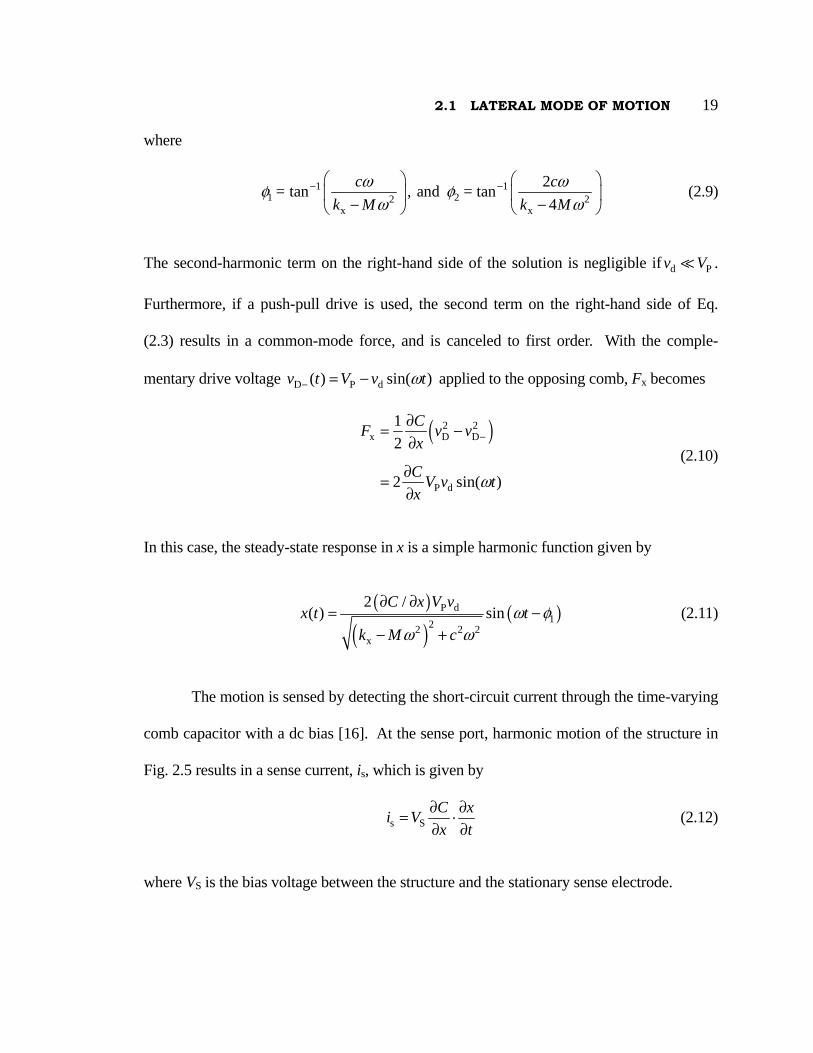
Figure 2.5 A linear resonator electrostatically driven from one side and sensed capacitively at the other side.

2.1 LATERAL MODE OF MOTION 18 the equation of motion is a second-order-differential equation given by
x x ( )Mx cx k x F t+ + = (2.4)
where M is the effective mass of the structure. Using the principle of superposition, the
steady-state solution of Eq. (2.4) is the sum of the steady-state solutions of the following
equations [42]:
2 2x P d
1 12 2
CMx cx k x V vx
∂ ⎛ ⎞+ + = +⎜ ⎟∂ ⎝ ⎠ (2.5)
x P d sin( )CMx cx k x V v tx
ω∂+ + =∂
(2.6)
2x d
1 cos(2 )4
CMx cx k x v tx
ω∂+ + = −∂
(2.7)
Therefore, the steady-state response is given by
( )
( )( )
( )
( )( )
2 2P d
x
P d122 2 2
x
2d
222 2 2x
1 1( )2 2
/sin
/cos 2
4 4 4
Cx t V vk x
C x V vt
k M c
C x vt
k M c
ω φω ω
ω φω ω
∂ ⎛ ⎞= +⎜ ⎟∂ ⎝ ⎠
∂ ∂+ −
− +
∂ ∂− −
− +
(2.8)
2.1 LATERAL MODE OF MOTION 19 where
1 11 22 2
x x
2tan and tan4
c c = , = k M k M
ω ωφ φω ω
− −⎛ ⎞ ⎛ ⎞⎜ ⎟ ⎜ ⎟
− −⎝ ⎠ ⎝ ⎠ (2.9)
The second-harmonic term on the right-hand side of the solution is negligible if d Pv V .
Furthermore, if a push-pull drive is used, the second term on the right-hand side of Eq.
(2.3) results in a common-mode force, and is canceled to first order. With the comple-
mentary drive voltage D P d( ) sin( )v t V v tω− = − applied to the opposing comb, Fx becomes
( )2 2
x D D
P d
12
2 sin( )
CF v vx
C V v tx
ω
−∂= −∂
∂=∂
(2.10)
In this case, the steady-state response in x is a simple harmonic function given by
( )
( )( )P d
122 2 2x
2 /( ) sin
C x V vx t t
k M cω φ
ω ω
∂ ∂= −
− + (2.11)
The motion is sensed by detecting the short-circuit current through the time-varying
comb capacitor with a dc bias [16]. At the sense port, harmonic motion of the structure in
Fig. 2.5 results in a sense current, is, which is given by
s SC xi Vx t
∂ ∂= ⋅∂ ∂
(2.12)
where VS is the bias voltage between the structure and the stationary sense electrode.

2.1 LATERAL MODE OF MOTION 20 Finally, the transconductance of the resonant structure is defined by S d( ) /G j I Vω = .
Substituting the time derivative of Eq. (2.8) into Eq. (2.12), we can express the output si in
terms of the input dv :
( )
( )( )
( )
( )( )
2P S d
s 122 2 2x
2 2S d
222 2 2x
/( ) cos
/sin 2
2 4 4
C x V V vi t t
k M c
C x V vt
k M c
ωω φ
ω ω
ωω φ
ω ω
∂ ∂= −
− +
∂ ∂+ −
− +
(2.13)
At this point, we simplify the analysis by assuming d Pv V , and thus the second-harmonic
term can be ignored. Therefore,
( )
( )( )1
2P S
22 2 2x
/( ) j tC x V V
G j t ek M c
ω φωω
ω ω
−∂ ∂=
− + (2.14)
The magnitude of ( )G j tω is doubled for the case of a push-pull drive. At mechanical
resonance, 2 2r x /k Mω ω= = , and the magnitude of the transconductance is evaluated to be
( )2r r P S
x( ) /QG j t V V C x
kω ω= ∂ ∂ (2.15)
where Q is the quality factor of the system, and is given by [42]
x
r
kQcω
= (2.16)
The value of ( )/C x∂ ∂ of the resonators can be evaluated experimentally by measuring
placehold.

2.1 LATERAL MODE OF MOTION 21 the quality factor and the transconductance at resonance and substituting the results in Eq.
(2.15).

22
2.2 VERTICAL MODE OF MOTION
One of the potential applications of lateral resonators actuated with the electrostatic comb
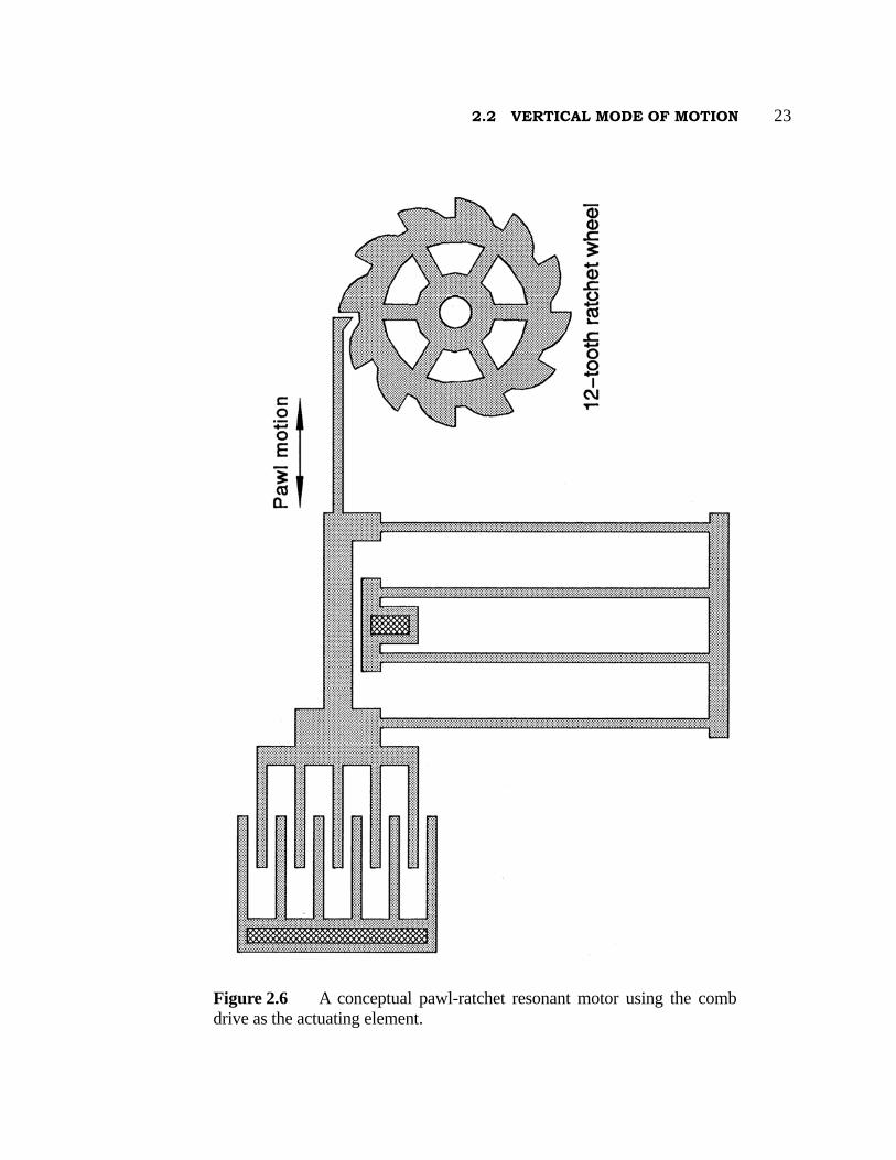
drive is resonant microactuators [30]. Figure 2.6 illustrates a schematic surface-
micromachined resonant micromotor based on a pawl-ratchet mechanism. For efficient
mechanical coupling between the vibrating pawl and the toothed wheel, it is essential that
both structures remain co-planar. However, 2 µm-thick polysilicon resonators with
compliant folded-beam suspensions have been observed to levitate over 2 µm when driven
by an electrostatic comb biased with a dc voltage of 30 V. The comb levitation results in an
unbalanced upward force applied to one side of the folded-beam suspension, causing the
pawl tip to deflect downward and to miss the ratchet wheel completely. Figure 2.7 shows a
possible outcome if the comb is levitated by more than the thickness of the polysilicon film.
This effect must be understood in order to design functioning resonant microactuators, with
the possibility that levitation by the comb structures may offer a convenient means for
selective pawl engagement.
In this section, the electrostatic forces responsible for levitation are analyzed, along
with the discussion of the modified comb design with independently biased fingers for
levitation control.
2.2.1 Origin of Induced Vertical Motion
Levitation phenomenon of the comb-drive structure is due to electrostatic repulsion by
image charges mirrored in the ground plane beneath the suspended structure. The ground
2.2 VERTICAL MODE OF MOTION 23
Figure 2.6 A conceptual pawl-ratchet resonant motor using the comb drive as the actuating element.

2.2 VERTICAL MODE OF MOTION 24
Figure 2.7 Cross section of the ratchet wheel and pawl tip after unbal-anced levitation force is induced on the comb structure.
2.2 VERTICAL MODE OF MOTION 25 plane is essential for successful electrostatic actuation of micromechanical structures
because of the need to shield the structures from relatively large vertical fields [43, 44].
It has been observed that if the underlying nitride and oxide passivation layers are not
covered with a grounded polysilicon shield, the application of a dc bias voltage will cause
the structures to be stuck down to the substrate. Furthermore, varying the bias voltage
causes the structures to behave unpredictably.
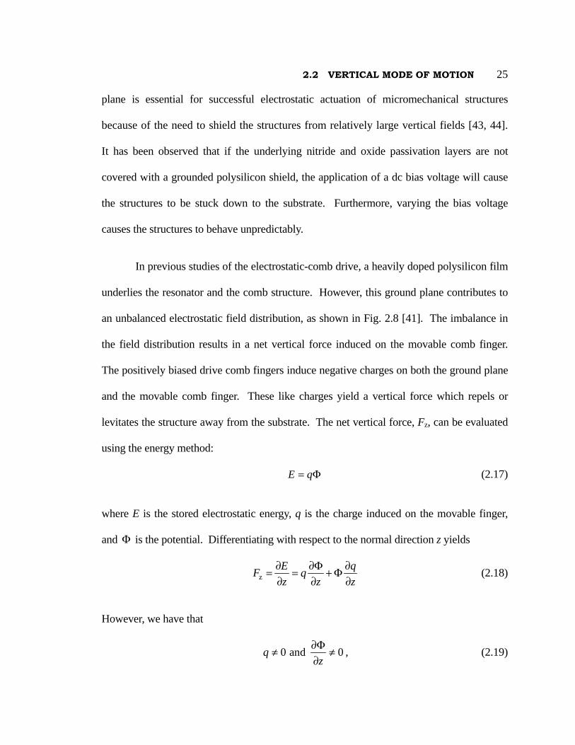
In previous studies of the electrostatic-comb drive, a heavily doped polysilicon film
underlies the resonator and the comb structure. However, this ground plane contributes to
an unbalanced electrostatic field distribution, as shown in Fig. 2.8 [41]. The imbalance in
the field distribution results in a net vertical force induced on the movable comb finger.
The positively biased drive comb fingers induce negative charges on both the ground plane
and the movable comb finger. These like charges yield a vertical force which repels or
levitates the structure away from the substrate. The net vertical force, Fz, can be evaluated
using the energy method:
E q= Φ (2.17)
where E is the stored electrostatic energy, q is the charge induced on the movable finger,
and Φ is the potential. Differentiating with respect to the normal direction z yields
zE qF qz z z
∂ ∂Φ ∂= = +Φ∂ ∂ ∂
(2.18)
However, we have that
0 and 0qz
∂Φ≠ ≠∂
, (2.19)

2.2 VERTICAL MODE OF MOTION 26
and thus,
z 0F ≠ . (2.20)
Whether this force causes significant static displacement or excites a vibrational mode of
the structure depends on the compliance of the suspension and the quality factor for vertical
displacements.
Figure 2.8 Cross section of the potential contours (dashed) and electric
fields (solid) of a comb finger under levitation force induced by two adjacent electrodes.
2.2 VERTICAL MODE OF MOTION 27 2.2.2 Finite-Element Simulation
Using Maxwell [41] to simulate the cross section of the comb fingers biased with a dc
voltage, we obtain the potential contour plots at different elevations, three of which are
shown in Figs. 2.9 to 2.11. The simulations provide simultaneous outputs of the vertical
force induced on the movable comb fingers. The vertical force, zF , is then plotted against
levitation, z, at different dc bias voltages, resulting in Fig. 2.12.
There are several important observations from Fig. 2.12. First, the stable
equilibrium levitation, 0z , is the same for any nonzero bias voltages. Thus, in the absence
of a restoring spring force, the movable comb fingers will be levitated to 0z upon the
application of a dc bias. Second, given z, zF is proportional to the square of the applied dc
bias, 2PV . And at any PV , zF is roughly proportional to (–z) as long as z is less than 0z .
Thus,
( ) ( )0 02 2
z P z z P 00 0
for z z z z
F V F V z zz z
γ− −
∝ ⇒ ≈ < (2.21)
where the constant of proportionality, zγ [pN·V–2], is defined as the vertical drive capacity.
An important interpretation of Eq. (2.21) is that since ( )zF z∝ − , the levitation
force behaves like an electrostatic spring, such that ( )z e 0F k z z= − , where ek is the

2.2 VERTICAL MODE OF MOTION 28
Figure 2.9 Maxwell output showing potential contours at z = 0.

2.2 VERTICAL MODE OF MOTION 29
Figure 2.10 Maxwell output at z = 1 µm.

2.2 VERTICAL MODE OF MOTION 30
Figure 2.11 Maxwell output at z = 2 µm.

2.2 VERTICAL MODE OF MOTION 31
electrostatic spring constant,
2
Pe z
0
Vkz
γ= (2.22)
Both Eqs. (2.21) and (2.22) will be used extensively in the following discussions on
vertical transfer function and vertical resonance.
Figure 2.12 Simulated Fz vs z at different VP. Fz is normalized to per-comb-finger (finger dimensions: h = g = 2 µm, w = 4 µm).

2.2 VERTICAL MODE OF MOTION 32 2.2.3 Vertical Transfer Function
The total vertical force acting on the comb fingers includes the levitation force, zF , and
the passive restoring spring force, kF , generated by the mechanical suspensions of the
system, as illustrated in Fig. 2.13. The vertical dc transfer characteristics can be
evaluated by solving
net z k 0F F F= − = (2.23)
where netF is the net force acting on the movable comb finger, and
k zF k z= (2.24)
Figure 2.13 The vertical forces acting on a movable comb finger.
2.2 VERTICAL MODE OF MOTION 33 where zk is the vertical spring constant. Substituting Eqs. (2.21) and (2.24) into Eq. (2.23)
we have
( )02
P0
0z zz z
V k zz
γ−
− = (2.25)
Solving for z in terms of PV yields
2
0 z P2
z 0 z P
z Vzk z V
γγ
=+
(2.26)
Equation (2.26) is plotted in Fig. 2.14. The initial slope of the curve is largely
dependent on zγ , which determines the threshold voltage where levitation reaches 90%
of the maximum, and the asymptotic value approaches 0z . Therefore, in certain
applications where vertical levitation is undesirable, both zγ and 0z should be minimized.
The method to control vertical levitation is discussed in section 2.2.5 of this chapter.
2.2.4 Vertical Resonant Frequency
In this section, we consider the case where the resonators are not damped vertically, such
as for the case of vibrations in vacuum. This assumption is justified on the ground that
the levitation force is much weaker than the force generated by a conventional vertically-
driven microbridge with an efficient parallel-plate-capacitor drive [16]. Therefore,
because of squeeze-film damping, vertical vibration in air is not significant for the weak
levitation force.

2.2 VERTICAL MODE OF MOTION 34
Thus, in the absence of damping, the governing equation of motion is a second-
order-differential equation, given by
2
net 2zF M
t∂=∂
(2.27)
where M is the effective mass of the vibrating structure.
The net vertical force, netF , which is zero in dc analysis [Eq. (2.23)], is now a
sinusoidal function when the bias voltage, PV , is replaced with a generalized drive
ddffdfff
Figure 2.14 Theoretical levitation (z) vs VP on dimensionless axes. The
scales on each axis are to be fitted to experimental results.

2.2 VERTICAL MODE OF MOTION 35 voltage, D ( )v t :
( )0 2
net z k z D z0
z zF F F v k z
zγ
−= − = − (2.28)
Thus, Eq. (2.27) becomes
( ) 2
0 2z D z 2
0
z z zv k z Mz t
γ− ∂− =
∂ (2.29)
For a drive voltage D ( )v t given by
D P d( ) sin( )v t V v tω= + (2.30)
where PV is the dc bias and dv is the ac drive amplitude, we can assume the sinusoidal
steady-state solution in z to be
P d( ) sin( )z t z z tω φ= + − (2.31)
where Pz is the average dc levitation, dz is the vibration amplitude, and φ is the phase
difference between the electrical drive signal and the mechanical response.
Substituting Eqs. (2.30) and (2.31) into Eq. (2.29) yields
[ ] [ ]
[ ]
20 P d2d z P d
0
z P d
sin( )sin( ) sin( )
sin( )
z z z tM z t V v t
z
k z z t
ω φω ω φ γ ω
ω φ
− + −− − = +
− + −
(2.32)

2.2 VERTICAL MODE OF MOTION 36 Since netF is zero when only dc bias is applied, we have
( )0 P 2
net z z Pd.c.0
0Pz z
F V k zz
γ−
= − = (2.33)
Using Eq. (2.33) to eliminate dc terms in Eq. (2.32) leads to
[ ]2 2 2zd 0 P d P d d
0
2zd P z d
0
sin( ) sin( ) 2 sin( ) sin ( )
sin( ) sin( )
M z t z z z t V v t v tz
z t V k z tz
γω ω φ ω φ ω ω
γ ω φ ω φ
⎡ ⎤− − = − − − +⎣ ⎦
− − − −(2.34)
At this point, in order to find the linear resonant behavior, we eliminate the second-
order terms:
2 20 P zd z P d P z d
0 0sin( ) 2 sin( ) sin( )z zM z t V v t V k z t
z zγω ω φ γ ω ω φ
⎛ ⎞−− − = − + −⎜ ⎟⎝ ⎠
(2.35)
Expressing dz in terms of dv :
0 Pz P d
0d
2 2zP z
0
2sin( ) sin( )
z z V vzz t t
V k Mz
γω φ ωγ ω
−
− =+ −
(2.36)
which describes a classical undamped system under harmonic force. The undamped
vertical resonant frequency, 1ω , under the influence of applied voltage can then be solved
as

2.2 VERTICAL MODE OF MOTION 37
12 2
z z P 01
/k V zMγω
⎛ ⎞+= ⎜ ⎟⎝ ⎠
(2.37)
and φ is identically zero for 1ω ω≠ .
An important observation is that the vertical resonant frequency is a strong function
of the applied dc bias, PV . If we define the mechanical resonant frequency (under zero
bias) as 0ω , such that
12z
0kM
ω ⎛ ⎞= ⎜ ⎟⎝ ⎠
(2.38)
We can quantify the frequency shift as a ratio given by
12 2
z z P 01
0 z
/k V zkγω
ω⎛ ⎞+= ⎜ ⎟⎝ ⎠
(2.1)
which is plotted in Fig. 2.15. The frequency ratio 1 2/ω ω asymptotically approaches a
straight line, such that
P
12
1 z
0 0 zlim
V z kω γω→∞
⎛ ⎞ ⎛ ⎞=⎜ ⎟ ⎜ ⎟
⎝ ⎠ ⎝ ⎠ (2.2)
Equation (2.39) is consistent with the observation made in section 2.2.2, that the
levitation force behaves like an electrostatic spring, with a spring constant 2e z P 0/k V zγ=

2.2 VERTICAL MODE OF MOTION 38
[Eq. (2.22)]. If we substitute Eq. (2.22) into Eq. (2.39), we then have
12
z e1
0 z
k kk
ωω
⎛ ⎞+= ⎜ ⎟⎝ ⎠
(2.3)
which shows that the electrostatic spring constant adds to the mechanical spring constant
for determining the resonant frequency.
The comb can therefore be useful for controlling the vertical resonance. In the
case where the vertical mechanical spring constant of the suspension is very close to the
Figure 2.15 Theoretical frequency ratio ω1/ω0 vs. VP on dimensionless axes. The scales on each axis are to be fitted to experimental results.
2.2 VERTICAL MODE OF MOTION 39 lateral one, i.e., z xk k≈ , the undesirable simultaneous excitation of both vertical and
lateral modes of motion can be conveniently avoided by shifting away the vertical
resonant frequency with a dc bias voltage.
2.2.5 Levitation Control Method
In addition to shifting the vertical resonant frequency, it is desirable to control the dc
levitation effect as well. There are several means to reduce the levitation force. By
eliminating the ground plane and removing the substrate beneath the comb structures with
bulk-micromachining techniques, the field distribution becomes balanced. Alternatively, a
top ground plane suspended above the comb drive will achieve a balanced vertical force on
the comb. However, both of these approaches require significantly more complicated
fabrication sequences.
A simpler solution is to modify the comb drive itself. Reversing the polarity on
alternating drive fingers results in an altered field distribution, as shown in Fig. 2.16.
Following the analysis in Eqs. (2.17) to (2.20), we now have 0Φ = and / 0z∂Φ ∂ ≈ , and
thus
z 0E qF qz z z
∂ ∂Φ ∂= = +Φ ≈∂ ∂ ∂
(2.4)
To further suppress levitation, the ground plane is modified such that underneath
each comb finger there is a strip of conductor biased at the same potential, as illustrated in
Fig. 2.17. The polysilicon layer is used to form the crossovers to electrically isolate
2.2 VERTICAL MODE OF MOTION 40
Figure 2.16 Cross section of the potential contours (dashed) and electric fields (solid) around a movable comb finger when differential bias is applied to the two adjacent electrodes.
Figure 2.17 Potential contours (dashed) and electric fields (solid) around
a movable comb finger when differential bias is applied to the two adjacent electrodes and the striped ground conductors.

2.2 VERTICAL MODE OF MOTION 41 alternating comb fingers (Fig. 2.18). Simulation shows that the levitation force is
suppressed by over an order of magnitude compared to the original biasing scheme.
Figure 2.18 Crossover layout for electrical isolation of alternating drive electrodes.

42
2.3 MECHANICAL ANALYSIS
In the previous sections, we have completed the analysis for both the lateral and vertical
electrostatic characterizations of the comb drive, using the terms xk and zk to represent
the mechanical spring constants. In this section, we will analyze various mechanical
spring designs for both classes of linear and torsional resonators, deriving equations for
the spring constants as well as for the lateral resonant frequencies. Finally, we will
discuss the quality factor Q.
2.3.1 Linear Lateral Resonant Structures
The design criteria for the suspensions of a large-amplitude, lateral resonator actuated
with comb drives are two-fold. First, the suspensions should provide freedom of travel
along the direction of the comb-finger motions (x), while restraining the structure from
moving sideways (y) to prevent the comb fingers from shorting to the drive electrodes.
Therefore, the spring constant along the y direction must be much higher than that along
the x direction, i.e., y xk k . Second, the suspensions should allow for the relief of the
built-in stress of the structural polysilicon film as well as axial stress induced by large
vibrational amplitudes.
Folded-beam suspension design fulfills these two criteria. Figure 1.3 (repeated
here as Fig. 2.19 for convenience) is the layout of a linear resonant structure supported by
a pair folded-beam suspensions. As we will show, this design allows large deflection in
the x direction (perpendicular to the length of the beams) while providing stiffness in
2.3 MECHANICAL ANALYSIS 43
placehold placehold placehold placehold placehold placehold placehold placehold
placehold
Figure 2.19 Layout of a linear resonant structure supported by a pair of folded-beam suspensions.

2.3 MECHANICAL ANALYSIS 44
the y direction (along the length of the beams). Furthermore, the only anchor points for the
whole structure are near the center, thus allowing the parallel beams to expand or contract
in the y direction, relieving most of the built-in and induced stress. This section describes
the analysis of the spring constant of the folded-beam support, the lateral resonant
frequency and the quality factor of lateral resonators similar to Fig. 2.19.
2.3.1.1 Spring Constant of Folded-Beam Support
Figure 2.20 shows the mode shape of the folded-beam support when the resonant plate is
statically displaced by a distance 0X under an applied force xF in the positive x
Figure 2.20 Mode shape of a folded-beam support when the resonant plate is displaced by X0 under a force of Fx.

2.3 MECHANICAL ANALYSIS 45
direction. Each of the beams has a length L, width w, and thickness h. We can simplify the
analysis by considering segment [AB], which is illustrated in Fig. 2.21. The following
analysis assumes that the outer connecting truss for the 4 beam segments is rigid, which is
justified because of its wider design. Therefore, as part of the boundary conditions, the
slopes at both ends of the beams are identically zero. Also, since geometric shortening in
the y direction is identical for all 4 beams, there is no induced axial stress as a result of
large deflections.
Since the resonant plate is supported by 4 identical beams, the force acting on
x
zfor2 3Fx(y)= (3 - 2 ) 0 y LLy y
4(12 )EI≤ ≤ (2.5)
Figure 2.21 Mode shape of segment [AB].

2.3 MECHANICAL ANALYSIS 46
each beam is x / 4F . The equation of deflection for [AB] is given by [45]
( ) ( )2 3x
z( ) 3 2 for 0
4 12Fx y Ly y y L
EI= − ≤ ≤ (2.43)
where E is the Young’s modulus for polysilicon and zI is the moment of inertia of the
beam cross section with respect to the z axis. Note that since this beam segment has a
slope of zero at either ends, it cannot be considered as a cantilever beam. Examining Fig.
2.20, we know that segment [AB] is deflected by 0 / 2X at point B. So with the boundary
condition of 0( ) / 2x L X= , we have
( )3 30 x
z
3x
0z
3 22 48
24
X F L LEI
F LXEI
= −
⇒ =
(2.44)
Thus, the system spring constant in the x direction is
x zx 3
0
24F EIkX L
= = (2.45)
Similarly, the equation for vertical deflection under an induced vertical force, Fz, is
given by
( )2 3z
x( ) 3 2 for 0
48Fz y Ly y y LEI
= − ≤ ≤ (2.46)
where xI is the moment of inertia with respect to the x axis. The vertical spring constant,
2.3 MECHANICAL ANALYSIS 47
zk , is
xz 3
24EIkL
= (2.47)
Finally, to complete the evaluation, we need to express the moments of inertia I in
terms of physical dimensions. For an ideal beam with rectangular cross section, having a
width w and a thickness h, the moments of inertia are [45]:
3 3
z x and 12 12hw h wI I= = (2.48)
However, due to fabrication difficulties, the cross section of the beams may be slightly
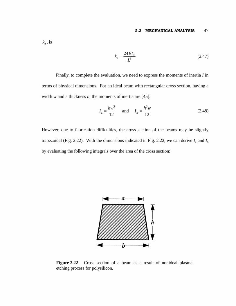
trapezoidal (Fig. 2.22). With the dimensions indicated in Fig. 2.22, we can derive Iz and Ix
by evaluating the following integrals over the area of the cross section:
Figure 2.22 Cross section of a beam as a result of nonideal plasma-etching process for polysilicon.

2.3 MECHANICAL ANALYSIS 48
( )( )
( )
2 2 2z
3 2 22
x
48
4
36( )
hI x dA a b a b
h a ab bI z dA
a b
= = + +
+ += =
+
∫
∫ (2.49)
It should be noted that since the cross sections of the beams are not far from being
rectangular, the shift in the neutral axis is negligible. Otherwise, second order effects must
be considered in stress calculations [46].
Due to the parallel-beam design, the suspension is very stiff in the y direction.
One possible mechanism that causes the resonant plate and the comb fingers to move
sideways is when four of the parallel beams are stretched while the other four are
compressed. The spring constant along the length of a beam, yk , is given by [45]
yAEkL
= (2.50)
where A is the cross-sectional area of the beam. As in the previous sections, we can
assume that the outer connecting trusses are rigid. Therefore, the ratio of the system
spring constant in the y direction ( y8k ) to that in the x direction [ xk , Eq. (2.45)] is
2 2
y3 3 2
x z
8 8 / 4 424 /
k AE L whL Lk EI L w h w
= = = (2.51)
For a typical folded-beam design with L = 200 µm and w = 2 µm, this ratio is evaluated
to be 40,000. Thus, motion in the y direction due to beam extension and compression is
very unlikely.

2.3 MECHANICAL ANALYSIS 49
Another possible mechanism that causes the structure to move sideways is when
at least 4 of the 8 parallel beams buckle under a force applied in the y direction, yF . As a
worst case consideration, we can use Euler’s simple buckling criterion to evaluate the
critical force, yF , required to buckle a pinned-pinned beam with length L [45]:
2
zy 2
EIFL
π= (2.52)
Comparing Eqs. (2.45) and (2.52), for a typical resonant structure with 200 µm-long
folded beams, the force yF required to buckle 4 of the supporting beams is over 60 times
higher than the force xF required to pull the structure statically by 5 µm in the x direction.
During vibration, xF required to sustain resonance is reduced by the quality factor Q,
which is typically between 20 to 100 in air, and 50,000 in vacuum. Furthermore, the most
probable origin of yF is comb-finger misalignment, which is very minimal because all the
critical features are defined with one mask during fabrication. Therefore, the folded-beam
design is attractive for structures actuated with dense comb drives.
An alternative suspension design for linear resonant structures is the “crab-leg”
flexure illustrated in Fig. 2.23 [47]. The advantage of this suspension is that the y x/k k
ratio can be designed to a given value by adjusting the dimensions of the crab-leg
segments. However, built-in stress is not relieved with this design because the
suspensions are anchored on the outer perimeter of the structure. Also, extensional axial
stress may become dominant during large-amplitude vibration.

2.3 MECHANICAL ANALYSIS 50
2.3.1.2 Spring Constant of Double-Folded Beams
A natural extension of the folded-beam suspension concept is the double-folded beam
design illustrated in Fig. 2.24. This design provides the advantage of compactness in
addition to all the benefits realized with the single-folded design. The spring constant for
the double-folded beam can be evaluated by recognizing that each of the 8 pairs of
parallel beams deflect by 0X /4 (compared to 0X /2 for the single-folded design), and each
of them experiences a force of xF /4 (Fig. 2.25). Thus, one of the boundary conditions
Figure 2.23 Crab-leg flexure design [47].

2.3 MECHANICAL ANALYSIS 51
Figure 2.24 Resonant structure suspended by a pair of double-folded beams.

2.3 MECHANICAL ANALYSIS 52
for segment [AB] becomes 0( )x L X= /4, resulting in
( )3 30 x
x
x z xx 32
0
3 24 48
122
X F L LEI
F EI kkX L
= −
⇒ = = =
(2.53)
where the subscript 2 denotes a double-folded system. This derivation can be further
extended to n-tuple-folded beam designs, each with 4n pairs of parallel beams. Upon the
application of a force xF to the system, each beam deflects by 0X /2n, leading to a
Figure 2.25 Mode shape of a double-folded suspension when the resonant plate is displaced by X0 under a force of Fx.

2.3 MECHANICAL ANALYSIS 53
boundary condition for each beam segment as 0( )x L X= /2n. Therefore,
30 x
x
x z xx 3
0
2 48
24n
X F Ln EI
F EI kkX nnL
=
⇒ = = =
(2.54)
2.3.1.3 Lateral Resonant Frequency
To evaluate the lateral resonant frequency of the original folded-beam system, we use
Rayleigh’s energy method [16]:
max max. . . .K E P E= (2.55)
where max. .K E is the maximum kinetic energy during a vibration cycle, and max. .P E is the
maximum potential energy. We will first evaluate max. .K E .
It is assumed that during the motion, the beams all displace with mode shapes
equal to their deflections under static loads. K.E. reaches its maximum when the structure
is at maximum velocity, and is given by
max p t b
2 2 2p p t t b b
. . . . . . . .
1 1 12 2 2
K E K E K E K E
v M v M v dM
= + +
= + + ∫ (2.56)
where M’s and v’s are the masses and maximum velocities, and subscripts p, t and b refer to
the plate, the sum of the two horizontal trusses and the sum of the eight parallel beam
segments, respectively. Since the horizontal trusses displace at half the velocity of the

2.3 MECHANICAL ANALYSIS 54
plate, we have
0p 0 t and
2Xv X vω ω= = (2.57)
And so the K.E. for the plate and the two horizontal trusses are
2 2 2p p p 0 p
1 1. .2 2
K E v M X Mω= = (2.58)
and
2 2t 0 t
1. .8
K E X Mω= (2.59)
The velocity profile of the beam segments is proportional to the mode shape at
maximum displacement. The mode shape is taken as the static displacement curve under
static loading, a common and sufficient assumption given that the beams do not resonate
themselves. We first consider beam segment [AB] (Fig. 2.21). The equation of deflection
[Eq. (2.43)] and one of the boundary conditions are repeated here for convenience:
( )2 3x
z( ) 3 2 for 0
48Fx y Ly y y LEI
= − ≤ ≤ (2.60)
and
3
0 x
z( )
2 48X F Lx L
EI= = (2.61)

2.3 MECHANICAL ANALYSIS 55
Substituting Eq. (2.61) into Eq. (2.60) to eliminate the F/ zEI term, we have
2 3
0( ) 3 22
X y yx yL L
⎡ ⎤⎛ ⎞ ⎛ ⎞= −⎢ ⎥⎜ ⎟ ⎜ ⎟⎝ ⎠ ⎝ ⎠⎢ ⎥⎣ ⎦
(2.62)
So the velocity profile for segment [AB] is
2 3
0b [AB]( ) 3 2
2X y yv y
L Lω
⎡ ⎤⎛ ⎞ ⎛ ⎞= −⎢ ⎥⎜ ⎟ ⎜ ⎟⎝ ⎠ ⎝ ⎠⎢ ⎥⎣ ⎦
(2.63)
leading to the K.E. for [AB] as
22 32 20
[AB] [AB]0
22 2 2 30 [AB]
0
2 20 [AB]
1. . 3 22 4
3 28
13280
L
L
X y yK E dML L
X M y y dyL L L
X M
ω
ω
ω
⎡ ⎤⎛ ⎞ ⎛ ⎞= −⎢ ⎥⎜ ⎟ ⎜ ⎟⎝ ⎠ ⎝ ⎠⎢ ⎥⎣ ⎦
⎡ ⎤⎛ ⎞ ⎛ ⎞= −⎢ ⎥⎜ ⎟ ⎜ ⎟⎝ ⎠ ⎝ ⎠⎢ ⎥⎣ ⎦
=
∫
∫ (2.64)
where [AB]M is the mass of the segment [AB].
Similarly, we proceed with evaluating [CD]. .K E by first finding the velocity profile:
2 3
b 0[CD]3( ) 12
y yv y XL L
ω⎡ ⎤⎛ ⎞ ⎛ ⎞= − −⎢ ⎥⎜ ⎟ ⎜ ⎟
⎝ ⎠ ⎝ ⎠⎢ ⎥⎣ ⎦ (2.65)
Then
22 2 2 30 [CD]
[CD]0
2 20 [CD]
3. . 12 2
83280
LX M y yK E dyL L L
X M
ω
ω
⎡ ⎤⎛ ⎞ ⎛ ⎞= − −⎢ ⎥⎜ ⎟ ⎜ ⎟⎝ ⎠ ⎝ ⎠⎢ ⎥⎣ ⎦
=
∫ (2.66)
2.3 MECHANICAL ANALYSIS 56
where [CD]M is the mass of segment [CD], and is identical to [AB]M . Since the total mass
of the 8 parallel beams is bM , we have
[AB] [CD] b18
M M M= = (2.67)
Therefore,
b [AB] [CD]
2 2 2 20 b 0 b
2 20 b
. . 4 . . 4 . .
13 83560 560
635
K E K E K E
X M X M
X M
ω ω
ω
= +
= +
=
(2.68)
Collecting the results in Eqs. (2.58), (2.59) and (2.68) and substituting them into Eq.
(2.56) yields
2 2max 0 p t b
1 1 6. .2 8 35
K E X M M Mω ⎛ ⎞= + +⎜ ⎟⎝ ⎠
(2.69)
We now evaluate max. .P E as the work done to achieve maximum deflection:
0 0
2max x x x 0
0 0
1. .2
X X
P E F dx k xdx k X= = =∫ ∫ (2.66)
Equating the right-hand sides of Eqs. (2.69) and (2.70) yields the final result for the
resonant frequency:

2.3 MECHANICAL ANALYSIS 57
2 2 2x 0 0 p t b
12
x
p t b
1 1 1 62 2 8 35
1 124 35
k X X M M M
k
M M M
ω
ω
⎛ ⎞= + +⎜ ⎟⎝ ⎠
⎛ ⎞⎜ ⎟
⇒ = ⎜ ⎟⎜ ⎟+ +⎝ ⎠
(2.71)
The denominator on the right-hand side of this equation can be lumped together as the
effective mass of the system, M:
p t b1 124 35
M M M M= + + (2.72)
such that
12xk
Mω ⎛ ⎞= ⎜ ⎟
⎝ ⎠ (2.73)
2.3.1.4 Quality Factor
One of the advantages of laterally-driven resonant structures is that the damping in the
lateral direction is much lower than in the vertical direction. Therefore, when operated in
air, undesired vertical motions are conveniently damped. There are a number of
dissipative processes during lateral motion, all of them affecting the quality factor Q.
The dominant influences include Couette flow underneath the plate, air drag on the top
surface, damping in the comb gaps and direct air resistance related to the thickness of the
structure [48] (Fig. 2.26). For a micron-sized gap between the plate and the substrate,
energy dissipation through Couette flow underneath the plate dominates strongly over air

2.3 MECHANICAL ANALYSIS 58
drag on the top surface. If we consider Couette flow alone, then we can estimate the
quality factor Q as [37,48]:
xp
dQ MkAμ
= (2.74)
where µ is the absolute viscosity of air (typically 1.8 × 10⁻⁵ N·s·m–2), d is the offset
between the plate and the substrate, and M is the effective mass of the resonator.
The other dissipative processes including air friction and turbulent flow generated
placehold
Figure 2.26 Major dissipative processes of a laterally-driven resonant plate.

2.3 MECHANICAL ANALYSIS 59
in the comb-finger gaps as well as direct air resistance are difficult to analyze. Since some
of the comb-drive structures studied in this thesis are designed with as many as 18 movable
comb fingers to maximize drive efficiency, air friction between the comb fingers may
become the dominant factor in determining Q in air for these structures, and need to be
evaluated experimentally [49]. Nevertheless, Eq. (2.74) serves as the upper bound for
attainable Q in air.
When resonated in vacuum, vibrational energy is mostly dissipated to the substrate
through the anchors [19], or in the polysilicon structure itself. The quality factor in vacuum
can be further improved by employing tuning-fork design techniques such that the
vibrating structures are dynamically balanced by being anchored only at the nodes of free
oscillation [50].
2.3.2 Torsional Lateral Resonant Structures
Another class of structures is driven into torsional resonance by a set of concentric
interdigitated electrodes. Figure 2.27 shows one of the designs with two Archimedean
spirals as supporting beams. An advantage of the torsional resonant structures is that they
are anchored only at the center, enabling radial relaxation of the built-in residual stress in
the polysilicon film. Another benefit of the torsional approach is that four or more pairs of
balanced concentric-comb structures can be placed at the perimeter of the ring, allowing a
high degree of flexibility for differential drive and sense. Since both the drive and the
sense ports are differentially balanced, excitation of undesired oscillation modes is avoided
and signal corruption by feedthrough is minimized.

2.3 MECHANICAL ANALYSIS 60
Figure 2.27 Layout of a torsional resonator with two spirals.

2.3 MECHANICAL ANALYSIS 61
2.3.2.1 Spiral Support
The torsional spring constant of the Archimedean spiral is given by [51]:
3
1 [µN·µm·rad ]12
EhWkLθ
−= (2.75)
where L, W and h are the unfolded length, width and thickness of the spiral, respectively.
The advantage of spiral spring is that high compliance can be achieved in a compact
space. However, the spring is equally compliant in all directions on the x-y plane [51],
making it less ideal as a support where motion restrictions in certain directions are
needed.
2.3.2.2 Serpentine Support
An alternative to the spiral spring as a support for torsional resonators is the serpentine
spring illustrated in Fig. 2.28. Finite-element program can be used conveniently to evaluate
the spring constants for serpentine springs. SuperSAP [52] has been used extensively to
simulate the spring constants of serpentine springs with various dimensions (Fig. 2.28).
Unlike spiral springs, the compliance of serpentine springs is anisotropic. The spring
constant along the length of the spring ( rk ) is much higher than perpendicular spring
constant ( tk ). This is particularly advantageous as supports for torsional resonators, where
translational motions are undesirable.
The simulation results for rk and tk are tabulated in Tables 2.II and 2.III.
Increasing the number of meanders ( mN ) at the expense of space improves the spring

2.3 MECHANICAL ANALYSIS 62
constant ratio, rk / tk , and also minimizes tk . Narrowing the meander width ( mW )
improves rk / tk , but tk also becomes higher. The spring constant ratio reaches the
maximum in the limiting case of mW = 0, where the spring becomes a cantilever beam.
For practical design consideration, both the number of meanders ( mN ) and mW should be
chosen to obtain an optimally small tk and a sufficiently large rk / tk ratio.
Figure 2.28 Dimensions of the serpentine spring.
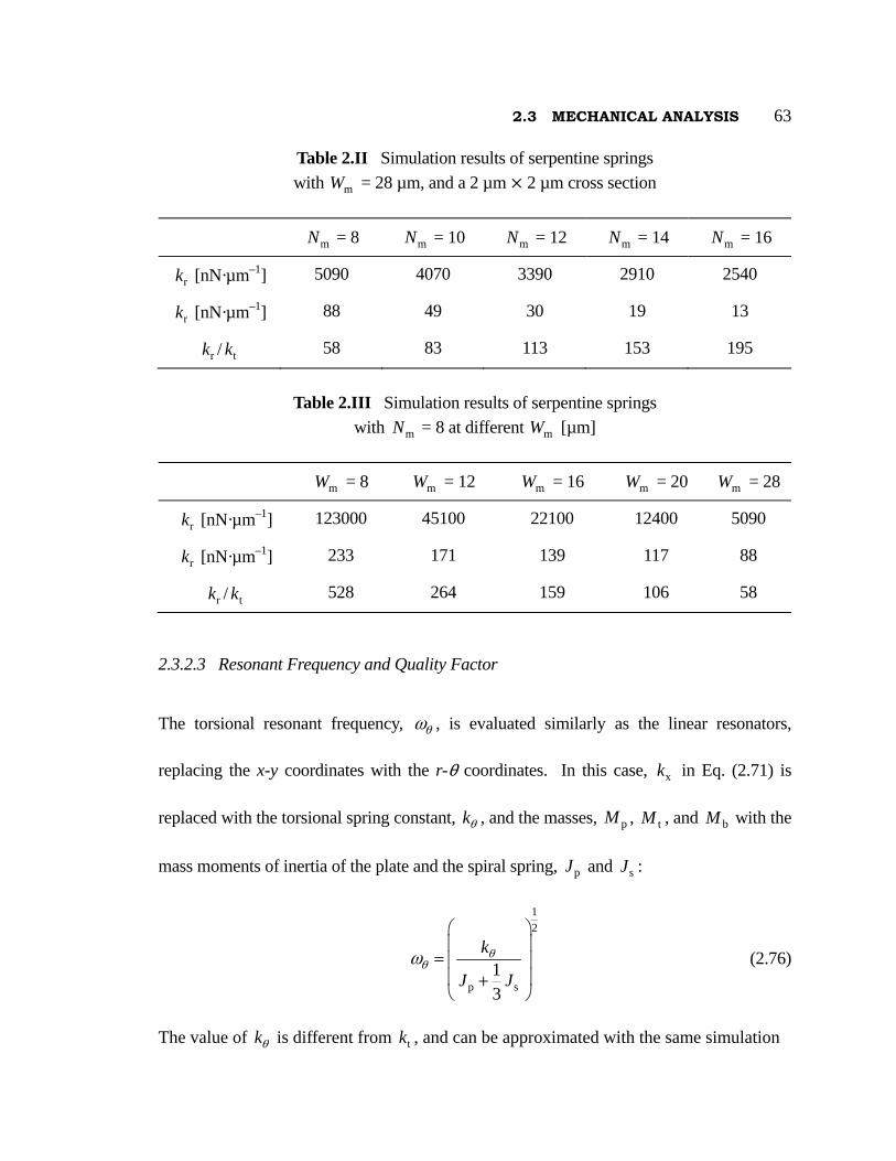
2.3 MECHANICAL ANALYSIS 63
Table 2.II Simulation results of serpentine springs with mW = 28 µm, and a 2 µm × 2 µm cross section
mN = 8 mN = 10 mN = 12 mN = 14 mN = 16
rk [nN·µm–1] 5090 4070 3390 2910 2540
rk [nN·µm–1] 88 49 30 19 13
rk / tk 58 83 113 153 195
Table 2.III Simulation results of serpentine springs with mN = 8 at different mW [µm]
mW = 8 mW = 12 mW = 16 mW = 20 mW = 28
rk [nN·µm–1] 123000 45100 22100 12400 5090
rk [nN·µm–1] 233 171 139 117 88
rk / tk 528 264 159 106 58
2.3.2.3 Resonant Frequency and Quality Factor
The torsional resonant frequency, θω , is evaluated similarly as the linear resonators,
replacing the x-y coordinates with the r-θ coordinates. In this case, xk in Eq. (2.71) is
replaced with the torsional spring constant, kθ , and the masses, pM , tM , and bM with the
mass moments of inertia of the plate and the spiral spring, pJ and sJ :
12
p s13
k
J Jθ
θω⎛ ⎞⎜ ⎟
= ⎜ ⎟⎜ ⎟+⎝ ⎠
(2.76)
The value of kθ is different from tk , and can be approximated with the same simulation
2.3 MECHANICAL ANALYSIS 64
program. The value of J can be found by evaluating the following integral over the
surface area of the structure or the spring:
2 3J r dM h r d drρ θ= =∫ ∫∫ (2.77)
where ρ is the density of polysilicon (2.3 × 10³ kg·m–3).
The quality factor is estimated similarly to Eq. (2.74) by assuming Couette flow
underneath the plate to be the dominant dissipation, and is given by
2p
dQ Jkr dA θμ
=∫
(2.78)
The same consideration concerning the role of air friction between the comb fingers
applies.

65
2.4 SUMMARY
We have discussed the first-order theory for the electrostatic characteristics of comb-drive
structures with respect to both the normal lateral mode of vibration as well as vertical
levitation effects. The results of these analyses form the foundation for designing laterally-
driven actuators with controlled vertical motion. The linearity of the lateral mode and the
frequency-shifting effect of the vertical mode greatly simplify the mode-decoupling
procedures. Differential biasing on alternating comb drive fingers can be employed to
suppress dc levitation by an order of magnitude. Finally, the mechanical-spring supports
including the folded-beam suspension for linear resonators and the spiral and serpentine
springs for torsional-resonant structures are analyzed. The folded-beam support (and the
extension to n-tuple-folded beams) is particularly advantageous for large-displacement
linear actuator applications.

66
Chapter 3
LATERAL STRUCTURE FABRICATION
The fabrication process for the electrostatic-comb drives and associated lateral structures
is a straightforward application of the surface-micromachining technology. Both plasma
and wet-chemical etchings are used to define features on different low-pressure chemical-
vapor-deposited (LPCVD) thin films, concluding with a final removal of a sacrificial
layer to free the suspended microstructures. This chapter highlights the important
processing steps, followed by a discussion on various performance-related fabrication
issues. The step-by-step process flow is detailed in Appendix A.
3.1 FABRICATION SEQUENCE
The structures are fabricated with the five-mask process illustrated in Fig. 3.1 [38,39]. A
significant advantage of this technology is that all the critical features are defined with
one mask, eliminating errors due mask-to-mask misalignment. The process begins with a
standard POCL3 blanket n+ diffusion, which defines the substrate ground plane, after
which the wafer is passivated with a layer of 1500 Å-thick LPCVD nitride deposited on
top of a layer of 5000 Å-thick thermal SiO2. Contact windows to the substrate ground
plane are then opened [Fig. 3.1(a)] using a combination of reactive-ion etching (RIE) in
an SF6 plasma and wet etching in 5:1 buffered-HF bath.

3.1 FABRICATION SEQUENCE 67
Figure 3.1 Process sequence of a lateral resonant structure.
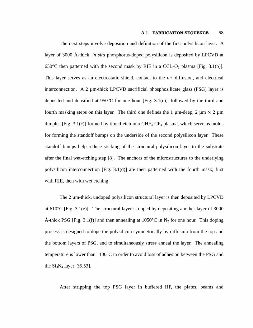
3.1 FABRICATION SEQUENCE 68
The next steps involve deposition and definition of the first polysilicon layer. A
layer of 3000 Å-thick, in situ phosphorus-doped polysilicon is deposited by LPCVD at
650°C then patterned with the second mask by RIE in a CCl4-O2 plasma [Fig. 3.1(b)].
This layer serves as an electrostatic shield, contact to the n+ diffusion, and electrical
interconnection. A 2 µm-thick LPCVD sacrificial phosphosilicate glass (PSG) layer is
deposited and densified at 950°C for one hour [Fig. 3.1(c)], followed by the third and
fourth masking steps on this layer. The third one defines the 1 µm-deep, 2 µm × 2 µm
dimples [Fig. 3.1(c)] formed by timed-etch in a CHF3-CF4 plasma, which serve as molds
for forming the standoff bumps on the underside of the second polysilicon layer. These
standoff bumps help reduce sticking of the structural-polysilicon layer to the substrate
after the final wet-etching step [8]. The anchors of the microstructures to the underlying
polysilicon interconnection [Fig. 3.1(d)] are then patterned with the fourth mask; first
with RIE, then with wet etching.
The 2 µm-thick, undoped polysilicon structural layer is then deposited by LPCVD
at 610°C [Fig. 3.1(e)]. The structural layer is doped by depositing another layer of 3000
Å-thick PSG [Fig. 3.1(f)] and then annealing at 1050°C in N2 for one hour. This doping
process is designed to dope the polysilicon symmetrically by diffusion from the top and
the bottom layers of PSG, and to simultaneously stress anneal the layer. The annealing
temperature is lower than 1100°C in order to avoid loss of adhesion between the PSG and
the Si3N4 layer [35,53].
After stripping the top PSG layer in buffered HF, the plates, beams and
placehold placehold.

3.1 FABRICATION SEQUENCE 69
electrostatic-comb drive and sense structures are defined in the final masking step [Fig.
3.1(g)]. The structures are anisotropically patterned by RIE in a CCl4 plasma, in order to
achieve nearly vertical sidewalls. Figure 3.1(h) illustrates the final cross section after the
wafer is immersed in 5:1 buffered HF to remove the sacrificial PSG. The wafer is then
left immersed in stagnant deionized (DI) water for at least two hours [54] followed by
repeated rinse until water resistivity reaches 16 MΩ-cm. The process concludes with
drying the wafer under an IR lamp for 10 minutes. Figures 3.2-3.10 are scanning-
electron and optical micrographs of the completed structures.
Figure 3.2 SEM of a linear resonator with 140 µm-long folded beams.

3.1 FABRICATION SEQUENCE 70
Figure 3.3 Optical micrograph of the alternating-comb structure with striped ground conductors underneath the comb fingers.
Figure 3.4 SEM of the alternating-comb drive showing the crossover structure.
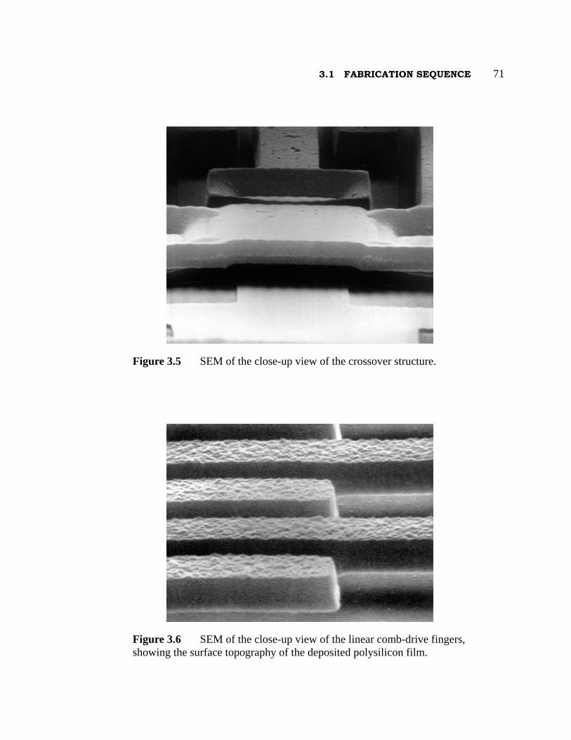
3.1 FABRICATION SEQUENCE 71
Figure 3.5 SEM of the close-up view of the crossover structure.
Figure 3.6 SEM of the close-up view of the linear comb-drive fingers, showing the surface topography of the deposited polysilicon film.
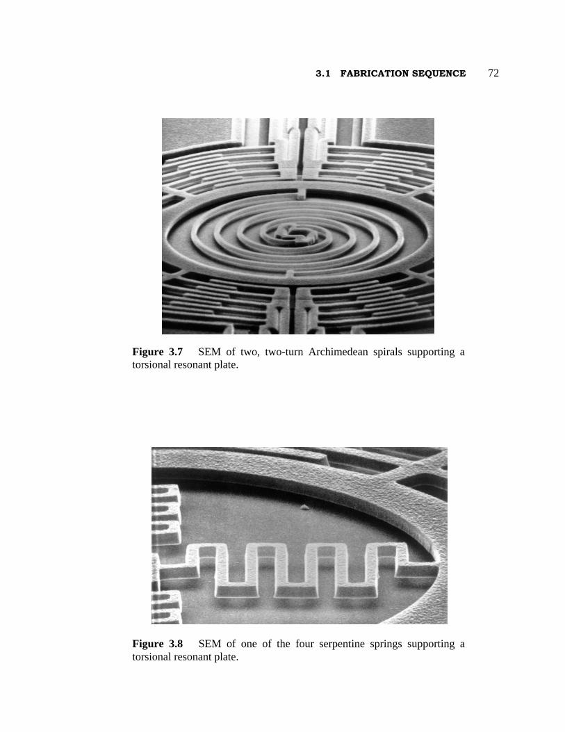
3.1 FABRICATION SEQUENCE 72
Figure 3.7 SEM of two, two-turn Archimedean spirals supporting a torsional resonant plate.
Figure 3.8 SEM of one of the four serpentine springs supporting a torsional resonant plate.

3.1 FABRICATION SEQUENCE 73
Figure 3.9 SEM of the concentric comb structure.
Figure 3.10 SEM of a structure supported by a pair of double-folded beams.
74
3.2 FABRICATION CHARACTERISTICS AND PERFORMANCE
Having described the fabrication sequence, we now identify and discuss several important
processing issues that affect the yield and performance of the finished structures.
3.2.1 Thin-Film Stress Consideration and Control Method
Residual stress in LPCVD polysilicon thin films has been a major design limitation for
micromechanical devices, which has motivated many research efforts for its characteriza-
tion and control [55-61]. In particular, the presence of strain gradients through the
thickness of the structural film results in suspended microstructures deflecting towards or
away from the substrate. Constrained structures, such as clamped-clamped beams, buckle
under compressive stress in the film [55].
The microstructures studied here can stick to the substrate after the final drying
process [62]. The yield of free-standing structures is zero on wafers for which the one-
hour stress anneal at 1050C is omitted (Fig. 3.11). When the stress anneal is included
in the process, 70% of the structures are free-standing. Most of the 30% which are
initially attached to the substrate are without standoff bumps, and can be easily freed with
a probe tip; the high flexibility of the structures allows manipulation without breakage.
No amount of probing, however, can free any of the unannealed structures.
A series of clamped-clamped diagnostic microbridges (Fig. 3.12) is included in
the design to estimate the average residual strain in the structural polysilicon film from
the minimum buckling length [56]. The moment of the residual strain is quantitatively
place
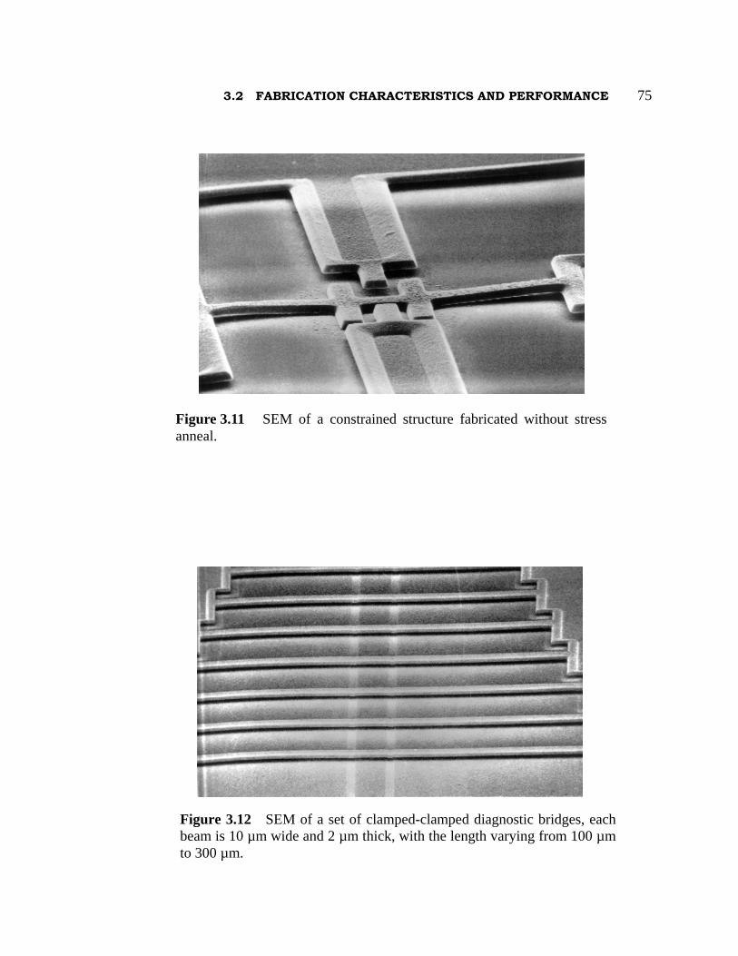
3.2 FABRICATION CHARACTERISTICS AND PERFORMANCE 75
Figure 3.11 SEM of a constrained structure fabricated without stress anneal.
Figure 3.12 SEM of a set of clamped-clamped diagnostic bridges, each beam is 10 µm wide and 2 µm thick, with the length varying from 100 µm to 300 µm.

3.2 FABRICATION CHARACTERISTICS AND PERFORMANCE 76
studied by a series of clamped-free cantilever beams. Since the microbridges have “step-
up” anchors, it is expected that end effects will have to be modeled carefully to obtain an
accurate value of the residual strain [57]. Moreover, the sticking of the diagnostic
microbridges and cantilevers to the substrate during drying is also a source of error in
calculating the strain and its moment [63].
For the unannealed samples, the cantilevers longer than 150 µm have a tendency to
deflect and attach to the substrate, while the minimum buckling length for microbridges is
about 120 µm (Fig. 3.13). Using Euler's simple criterion for buckling a clamped-clamped
beam [56], the strain is estimated to be 10–3. Annealed samples have apparently
undeflected cantilevers under optical and SEM observation and have a buckling length of
about 220 µm (Fig. 3.14), indicating a residual strain of about 3 × 10⁻⁴. These estimated
values are typical of residual strain for phosphorus-doped polysilicon [56].
However, annealing temperatures higher than 1100°C may adversely affect the
adhesion of PSG to stoichiometric-nitride passivation layer; and PSG on top of silicon-
rich nitride blisters at temperature higher than 1000°C. Figure 3.15 shows a wafer with
PSG on silicon-rich nitride damaged as a result of annealing at 1050°C for one hour.
Furthermore, if CMOS devices are present, the temperature ceiling is further reduced to
less than 900°C [64], where stress annealing is ineffective. Other processing approaches
such as rapid-thermal annealing (RTA) [65] or the use of as-deposited low-stress
polysilicon film [61] are possible alternatives.
Although stoichiometric nitride is preferred if high annealing temperature cannot

3.2 FABRICATION CHARACTERISTICS AND PERFORMANCE 77
Figure 3.13 Optical micrograph of a set of diagnostic microbridges from an unannealed wafer. Nomaski illumination reveals that bridges 120 µm and longer are buckled.
Figure 3.14 Optical micrograph of a set of microbridges from an annealed wafer. Nomaski illumination shows a buckling length of 220 µm.
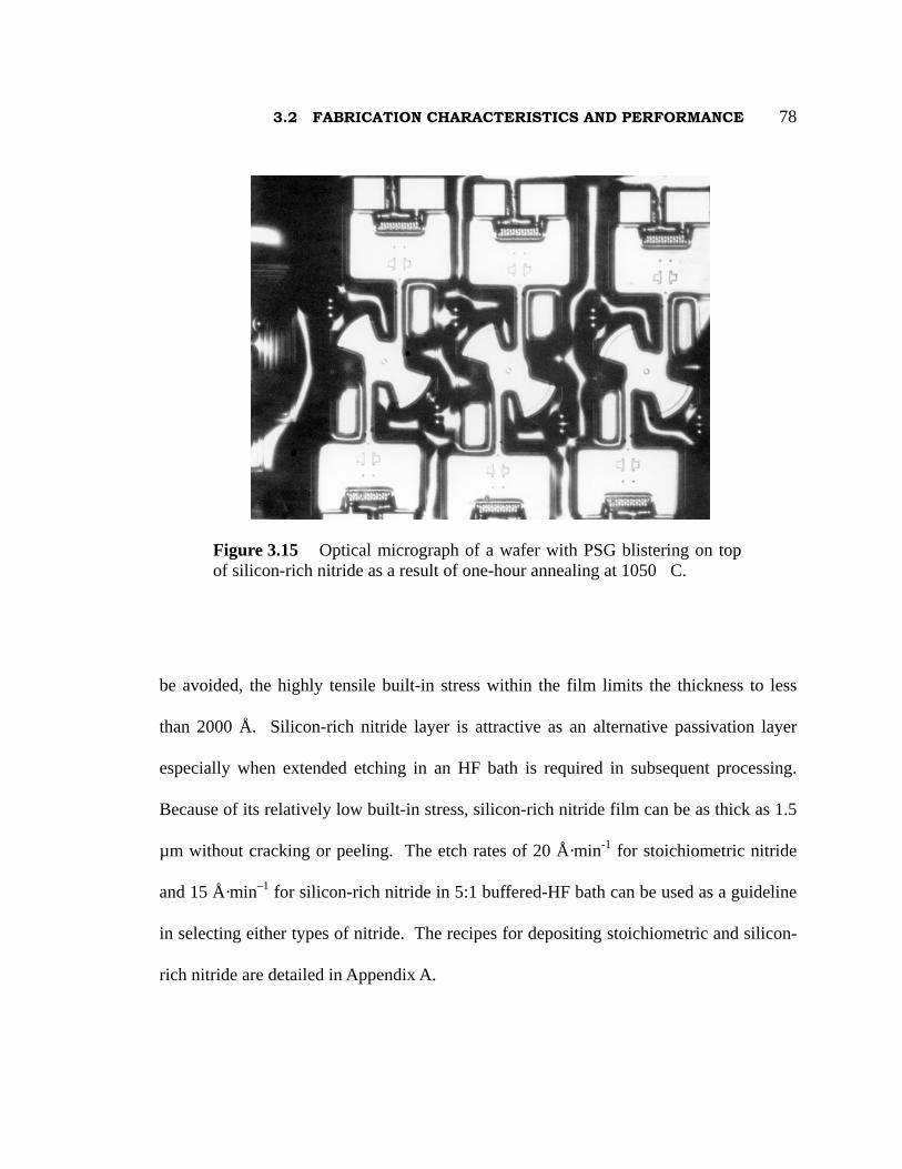
3.2 FABRICATION CHARACTERISTICS AND PERFORMANCE 78
be avoided, the highly tensile built-in stress within the film limits the thickness to less
than 2000 Å. Silicon-rich nitride layer is attractive as an alternative passivation layer
especially when extended etching in an HF bath is required in subsequent processing.
Because of its relatively low built-in stress, silicon-rich nitride film can be as thick as 1.5
µm without cracking or peeling. The etch rates of 20 Å·min-1 for stoichiometric nitride
and 15 Å·min–1 for silicon-rich nitride in 5:1 buffered-HF bath can be used as a guideline
in selecting either types of nitride. The recipes for depositing stoichiometric and silicon-
rich nitride are detailed in Appendix A.
Figure 3.15 Optical micrograph of a wafer with PSG blistering on top of silicon-rich nitride as a result of one-hour annealing at 1050C.
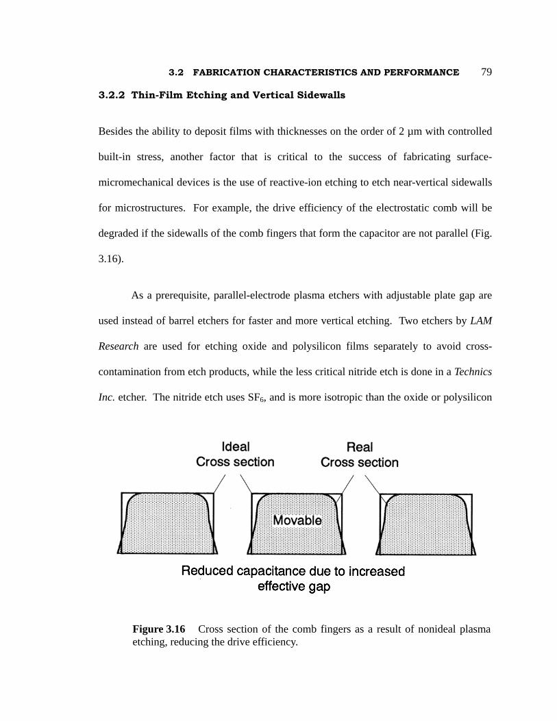
3.2 FABRICATION CHARACTERISTICS AND PERFORMANCE 79
3.2.2 Thin-Film Etching and Vertical Sidewalls
Besides the ability to deposit films with thicknesses on the order of 2 µm with controlled
built-in stress, another factor that is critical to the success of fabricating surface-
micromechanical devices is the use of reactive-ion etching to etch near-vertical sidewalls
for microstructures. For example, the drive efficiency of the electrostatic comb will be
degraded if the sidewalls of the comb fingers that form the capacitor are not parallel (Fig.
3.16).
As a prerequisite, parallel-electrode plasma etchers with adjustable plate gap are
used instead of barrel etchers for faster and more vertical etching. Two etchers by LAM
Research are used for etching oxide and polysilicon films separately to avoid cross-
contamination from etch products, while the less critical nitride etch is done in a Technics
Inc. etcher. The nitride etch uses SF6, and is more isotropic than the oxide or polysilicon
Figure 3.16 Cross section of the comb fingers as a result of nonideal plasmaetching, reducing the drive efficiency.

3.2 FABRICATION CHARACTERISTICS AND PERFORMANCE 80
etches.
For critically long etch steps such as those needed to open anchor windows for the
microstructures through the 2 µm-thick sacrificial-PSG layer and for patterning the
structural-polysilicon films, double photoresist layers (2 µm thick), hardened by baking at
120°C for at least 5 hours, are used as the etch mask. Also, we repeat several short etch
steps between 30-second to 1-minute duration with at least one minute idle between etches
to avoid excessive heat buildup [54]. If the reactive interface is allowed to heat up in a long
etch step, the masking photoresist will erode prematurely and the etch rate becomes
unpredictable. The radio-frequency (RF) power, the flow rates of different gases and the
electrode gap are optimized to obtain the most vertical sidewalls with sufficient selectivities
with respect to the photoresist and the underlying film. The optimized recipe is detailed in
Appendix A. Other work done at Berkeley has used a thin-PSG layer as a mask for etching
2 µm-thick undoped polysilicon films with promising results [66–68].
When etched in a CHF3-CF4 plasma, the selectivity of PSG with respect to either
silicon or silicon nitride is poor. Therefore, with a carefully characterized etch rate before
each run, the etch is timed to leave about 3000 Å or more of PSG, which is subsequently
removed by a highly selective timed etch in a 5:1 buffered-HF bath. Another complication
is that small windows are etched slower than bigger ones in the reactive-ion etcher. A 5 µm × 5 µm opening may be cleared at only half the rate of a completely exposed PSG film.
Longer wet-etch time must be allowed to clear contact holes of all sizes. Therefore, a
maximum of 1 µm undercut on anchor contacts may result, which must be compensated
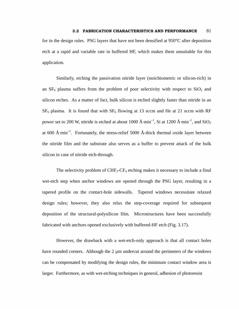
3.2 FABRICATION CHARACTERISTICS AND PERFORMANCE 81
for in the design rules. PSG layers that have not been densified at 950°C after deposition
etch at a rapid and variable rate in buffered HF, which makes them unsuitable for this
application.
Similarly, etching the passivation nitride layer (stoichiometric or silicon-rich) in
an SF6 plasma suffers from the problem of poor selectivity with respect to SiO2 and
silicon etches. As a matter of fact, bulk silicon is etched slightly faster than nitride in an
SF6 plasma. It is found that with SF6 flowing at 13 sccm and He at 21 sccm with RF
power set to 200 W, nitride is etched at about 1000 Å·min–1, Si at 1200 Å·min–1, and SiO2
at 600 Å·min–1. Fortunately, the stress-relief 5000 Å-thick thermal oxide layer between
the nitride film and the substrate also serves as a buffer to prevent attack of the bulk
silicon in case of nitride etch-through.
The selectivity problem of CHF3-CF4 etching makes it necessary to include a final
wet-etch step when anchor windows are opened through the PSG layer, resulting in a
tapered profile on the contact-hole sidewalls. Tapered windows necessitate relaxed
design rules; however, they also relax the step-coverage required for subsequent
deposition of the structural-polysilicon film. Microstructures have been successfully
fabricated with anchors opened exclusively with buffered-HF etch (Fig. 3.17).
However, the drawback with a wet-etch-only approach is that all contact holes
have rounded corners. Although the 2 µm undercut around the perimeters of the windows
can be compensated by modifying the design rules, the minimum contact window area is
larger. Furthermore, as with wet-etching techniques in general, adhesion of photoresist
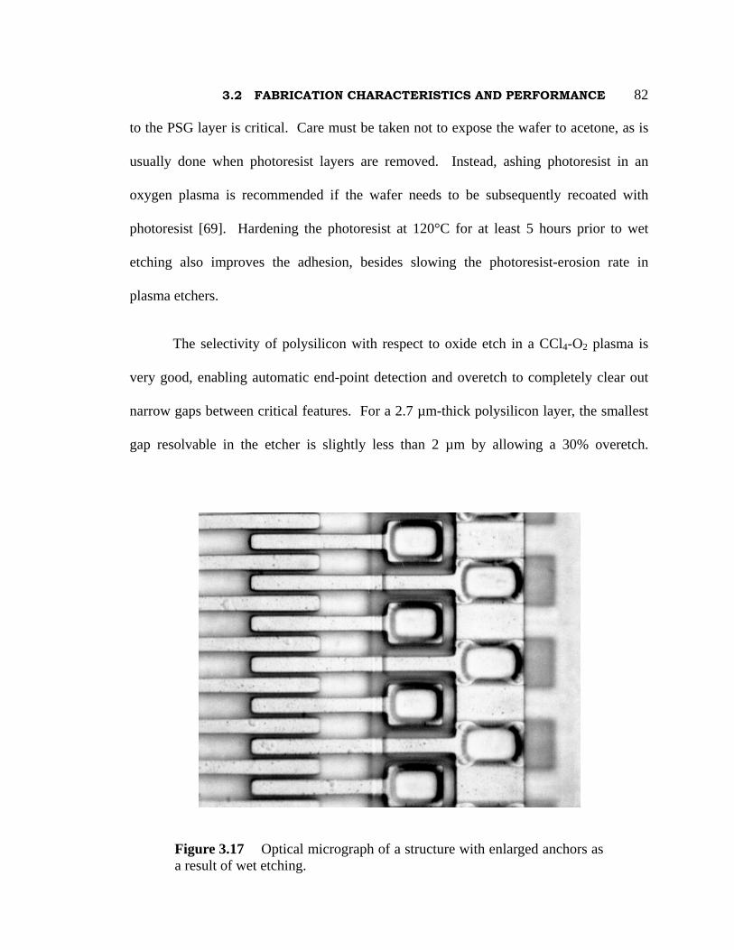
3.2 FABRICATION CHARACTERISTICS AND PERFORMANCE 82
to the PSG layer is critical. Care must be taken not to expose the wafer to acetone, as is
usually done when photoresist layers are removed. Instead, ashing photoresist in an
oxygen plasma is recommended if the wafer needs to be subsequently recoated with
photoresist [69]. Hardening the photoresist at 120°C for at least 5 hours prior to wet
etching also improves the adhesion, besides slowing the photoresist-erosion rate in
plasma etchers.
The selectivity of polysilicon with respect to oxide etch in a CCl4-O2 plasma is
very good, enabling automatic end-point detection and overetch to completely clear out
narrow gaps between critical features. For a 2.7 µm-thick polysilicon layer, the smallest
gap resolvable in the etcher is slightly less than 2 µm by allowing a 30% overetch.
Figure 3.17 Optical micrograph of a structure with enlarged anchors as a result of wet etching.
3.2 FABRICATION CHARACTERISTICS AND PERFORMANCE 83
Although increased overetch may clear out even smaller gaps, the resulting extended
photoresist erosion may cause rounding of the top edges and loss in feature resolution.
3.2.3 Single-Mask Process
The power and flexibility of the lateral-drive approach can be further demonstrated with
the single-mask process. Since all the critical features of the basic electrostatic-comb
drive are fabricated out of the same structural polysilicon layer, it is possible to include
only one photolithography step in the process to built a functioning comb structure, as
illustrated in Fig. 3.18.
The fabrication steps are similar with the complete process flow described in
section 3.1 with two exceptions. First, all lithography steps other than the one required to
pattern the structural polysilicon layer are omitted. Second, the final sacrificial etch with
buffered HF is carefully timed to free the moving parts of the structures but leave some
PSG under the polysilicon layer as pedestal anchors. The layouts of the structures are
redesigned to include large pad areas where PSG pedestals are needed, and etch holes are
distributed over the moving parts to ensure their quick release. Figure 3.19 is a sample
layout of a single-mask resonator.
Besides simplicity in processing, quick turn-around and high yield, single-mask
resonators offer additional advantages. With the absence of anchor windows, extended
PSG etching in plasma and step-coverage problems are eliminated. The sacrificial PSG
layers can then be made as thick as the deposition step allows, increasing the distance

3.2 FABRICATION CHARACTERISTICS AND PERFORMANCE 84
Figure 3.18 Single-mask processing steps.

3.2 FABRICATION CHARACTERISTICS AND PERFORMANCE 85
Figure 3.19 Layout of a single-mask resonator.

3.2 FABRICATION CHARACTERISTICS AND PERFORMANCE 86
between the resonator and the substrate ground plane. Damping due to air drag (Couette
flow) underneath the resonant plate is minimized (see sections. 2.3.1.3 and 2.3.2.3), and
the induced levitation force on the structure from the image charges on the ground plane
becomes less significant (see section 2.2.1).
The drawbacks, however, are that the big pads required to form the PSG pedestals
preclude a compact resonator design, and crossovers for electrical isolation to form the
differentially-balanced, alternating-comb drives (see section 2.2.5) are no longer
available. Nevertheless, for certain applications such as diagnostic test structures for
material properties, the fabrication simplicity may far outweigh these shortcomings.
Besides polysilicon as structural material and PSG as sacrificial layer, other
alternatives exist that involve different technologies. These possibilities are explored in
the final chapter.

87
3.3 SUMMARY
In this chapter, we have described the polysilicon surface-micromachining techniques for
fabricating the laterally-driven microstructures. The five-mask process involves standard
equipments available in a conventional IC-fabrication laboratory. The performance of the
finished structures is critically dependent on the mechanical characteristics of the
deposited polysilicon layer, especially the built-in stress within the film. The effects of
stress annealing at high temperature and the final sacrificial etch affect the choice of the
passivation nitride layer. Different combinations of plasma- and wet-etching techniques
are optimized to obtain the most vertical sidewalls. Finally, we have described the single-
mask process that offers the advantages of simplicity and functionality to demonstrate the
power and flexibility of the lateral-drive approach.
88
Chapter 4
TESTING TECHNIQUES AND RESULTS
This chapter presents a collection of the test results from three different process runs.
The first run includes both linear and torsional resonator prototypes with different
characteristics to verify the basic principles of the lateral-drive approach and to
demonstrate fabrication feasibility [38]. The second test chip is used to further
characterize the electromechanical behaviors of the comb-drive structures [39]. The final
test run is dedicated to study the vertical mode of motions and to compare the
effectiveness of various control methods [40]. The experimental results from these three
runs are organized to parallel Chapter 2, in which we have developed the first-order
theory for both the lateral and vertical modes of operations of the electrostatic-comb
drive.
The testing techniques involved in these experiments are first described. We then
discuss the experimental results of the lateral motions of the linear and torsional
resonators, followed by an analysis of the data collected on the vertical behavior of the
microstructures. We are mainly interested in the resonant frequencies and quality factors
of different resonator prototypes, from which we deduce the Young’s modulus of the
polysilicon film used and verify the first-order theory developed in Chapter 2.

89
4.1 TESTING TECHNIQUES
Since the vibration amplitudes of the resonators are sufficiently large (as much as 10 to
20 µm laterally), direct observations under a microscope as well as inside a scanning-
electron microscope (SEM) can be used to collect reasonably accurate data. Electrical
testing techniques that circumvent direct-signal feedthrough are developed to objectively
verify the observed results.
4.1.1 Direct Observations
An optically-based, wafer-level test setup includes a probe station with a set of zoom
objectives capable of 1000× maximum magnification, four probe-tip manipulators, and a
video camera. The optical-light source assembly can be optionally modified and replaced
with a stroboscopic light, the frequency of which can be triggered externally. Signals are
fed to the wafer under test through a series resistor (≥ 1 MΩ) to provide short-circuit
protection. The electronic equipment used is conventional, including dc voltage sources
with a maximum output of 50 V, function generators capable of 1 MHz sinewave output
at 10 V zero-to-peak amplitude, digital multimeters, and oscilloscopes.
Both sinusoidal and dc bias voltages are applied to the structures via probes
contacting the numbered polysilicon pads, as illustrated in Figs. 4.1 and 4.2. For the
linear structures, the sinusoidal drive voltage is applied to one set of fixed electrode
fingers via pad 1, while a dc bias is supplied to pad 2 (connected to the dormant sense
fingers) and pad 3 (connected to the first-level polysilicon ground plane and to the
placehold placehold placehold placehold placehold placehold placehold placehold
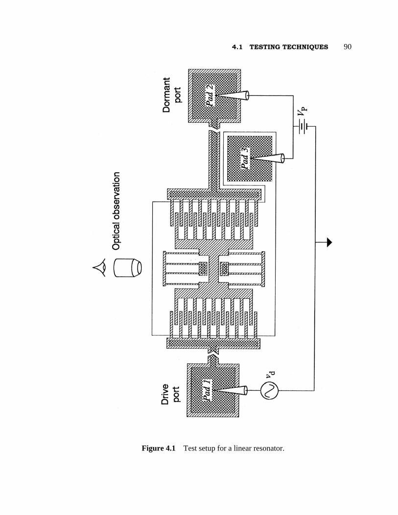
4.1 TESTING TECHNIQUES 90
placehold placehold placehold placehold placehold placehold placehold placehold
placehold placehold placehold placehold placehold placehold placehold placehold
placehold placehold placehold placehold placehold placehold placehold placehold
placehold placehold placehold placehold placehold placehold placehold placehold
placehold placehold placehold placehold placehold placehold placehold placehold
placehold placehold placehold placehold placehold placehold placehold placehold
placehold placehold placehold placehold placehold placehold placehold placehold
placehold placehold placehold placehold placehold placehold placehold placehold
placehold placehold placehold placehold placehold placehold placehold placehold
placehold placehold placehold placehold placehold placehold placehold placehold
placehold placehold placehold placehold placehold placehold placehold placehold
placehold placehold placehold placehold placehold placehold placehold placehold
placehold placehold placehold placehold placehold placehold placehold placehold
placehold placehold placehold placehold placehold placehold placehold placehold
placehold placehold placehold placehold placehold placehold placehold placehold
placehold placehold placehold placehold placehold placehold placehold placehold
placehold placehold placehold placehold placehold placehold placehold placehold
placehold placehold placehold placehold placehold placehold placehold placehold
placehold placehold placehold placehold placehold placehold placehold placehold
placehold placehold placehold placehold placehold placehold placehold placehold
placehold placehold placehold placehold placehold placehold placehold placehold
placehold placehold placehold placehold placehold placehold placehold placehold
placehold placehold placehold placehold placehold placehold placehold placehold
Figure 4.1 Test setup for a linear resonator.

4.1 TESTING TECHNIQUES 91
placehold placehold placehold placehold placehold placehold placehold placehold
placehold placehold placehold placehold placehold placehold placehold placehold
placehold placehold placehold placehold placehold placehold placehold placehold
placehold placehold placehold placehold placehold placehold placehold placehold
placehold placehold placehold placehold placehold placehold placehold placehold
placehold placehold placehold placehold placehold placehold placehold placehold
placehold placehold placehold placehold placehold placehold placehold placehold
placehold placehold placehold placehold placehold placehold placehold placehold
placehold placehold placehold placehold placehold placehold placehold placehold
placehold placehold placehold placehold placehold placehold placehold placehold
placehold placehold placehold placehold placehold placehold placehold placehold
placehold placehold placehold placehold placehold placehold placehold placehold
placehold placehold placehold placehold placehold placehold placehold placehold
placehold placehold placehold placehold placehold placehold placehold placehold
placehold placehold placehold placehold placehold placehold placehold placehold
placehold placehold placehold placehold placehold placehold placehold placehold
placehold placehold placehold placehold placehold placehold placehold placehold
placehold placehold placehold placehold placehold placehold placehold placehold
placehold placehold placehold placehold placehold placehold placehold placehold
placehold placehold placehold placehold placehold placehold placehold placehold
placehold placehold placehold placehold placehold placehold placehold placehold
placehold placehold placehold placehold placehold placehold placehold placehold
placehold placehold placehold placehold placehold placehold placehold placehold
Figure 4.2 Test setup for a torsional resonator.

4.1 TESTING TECHNIQUES 92
suspended structure through the folded-beams). The diffused ground plane is electrically
tied to the first polysilicon layer through a contact window (not shown in the drawing).
For the torsional structure in Fig. 4.2, the sinusoidal voltage is applied to the drive fingers
via pad 1, and the dormant sense fingers, ground plane and resonant structure are biased
via pad 2 and pad 3.
In order to provide large-amplitude lateral motion in air for visual observation, dc
biases of up to 40 V and drive-voltage amplitudes (zero-to-peak) of up to 10 V are used.
Resonant frequencies are determined by tuning the frequency of the function generator
until the blur envelope of the vibrating structure observed through the eyepieces or on the
video monitor reaches a maximum. Some of the structures are designed with a vernier
scale, which makes the amplitude estimation more accurate. The –3 dB bandwidth of the
vibration is then estimated by tuning the driving frequency away from resonance, until
the blur decreases to roughly 70% of the maximum. The quality factor Q is then deduced
from the –3 dB bandwidth using the following formula:
r
2 1
fQf f
=−
(4.1)
where rf is the resonant frequency and ( 2 1f f− ) is the –3 dB bandwidth. The results
from Eq. (4.1) are combined with the recorded dc bias and drive voltage level to evaluate
∂C/∂x using Eqs. (2.11) and (2.16).
The experiment is repeated with the microscope light assembly replaced with a
strobe light, which is triggered at a frequency 100 times less than that of the ac drive.

4.1 TESTING TECHNIQUES 93 Besides providing a more stable image, the mode shape of the resonating structure can
also be observed.
Finally, for testing under vacuum inside an SEM, the wafer is diced and bonded in
a standard dual-in-line package (DIP), which is then mounted at a tilt angle inside the
SEM chamber (Fig. 4.3). The SEM acceleration voltage is limited to about 1.6 kV to
minimize charging from the scanning electron beams. Electrical signals are supplied to
the chip with connectors through the chamber. The HP 4192A LF Impedance Analyzer is
used as a signal generator for vacuum testing because of its capability to resolve
Figure 4.3 Test setup using an SEM.
4.1 TESTING TECHNIQUES 94
frequencies at 10–3 Hz step and to generate signals at voltage amplitude down to 5 mV
level with 1 mV steps.
Although cumbersome and time-consuming to set up, testing inside an SEM
provides many advantages. First, in the absence of air damping, the measured resonant
frequencies are very accurate because of the extremely narrow bandwidth. The dc bias
and drive voltages required to sustain the high-Q resonance can also be lowered to 5 V
and 50 mV amplitude respectively, and thus possible nonlinear effects due to large drive
voltages are minimized. Furthermore, vertical motions are very difficult to observe using
the optical techniques because the mechanical vibrations are in the line of vision. Also,
since visual observation of resonance relies on maximizing the vibration amplitude, the
low Q due to heavy squeeze-film damping in air hampers accurate measurements of the
vertical resonant frequencies. Testing the sample mounted at a tilt angle inside the SEM
avoids these problems associated with vertical-mode testing.
Testing by direct observation requires careful judgement on the part of the
operator in deciding the size of the blur envelope of a vibrating structure, therefore, in
order to minimize relative errors between data points, testing must be done in a consistent
manner by the same operator without interruption during data collection.
4.1.2 Electrical Testing
To objectively verify the results obtained by observation, electrical testing techniques are
developed. Both the linear resonator (Fig. 4.1) and the torsional structure (Fig. 4.2) are
placehold placehold placehold placehold placehold placehold placehold placehold

4.1 TESTING TECHNIQUES 95
originally designed to allow for electrical detection of the structural vibration. In the two-
port arrangement, an HP 4195 Spectrum Analyzer would be connected to pad 2 of either
structures through a transimpedance amplifier to sense the current induced in the sense
electrode by motion of the structure.
However, the weak motional current is difficult to detect without an on-chip buffer
circuit [65]. Furthermore, the direct signal feedthrough from the drive port to the sense
electrode through the large probe-to-probe parasitic capacitance is at least 10 times stronger
than the desired motional signal.
To circumvent this problem, a modulation technique is used [70], in which a high-
frequency ac signal is superimposed on top of the dc bias applied to the structure through the
ground plane, as shown in Fig. 4.4. This signal serves as a carrier which is modulated by the
time-varying sense capacitance. As a result, electrical feedthrough from fixed parasitic
capacitors and the sense current due to the vibrating structure are separated in the frequency
domain.
An alternative approach without the use of a carrier signal is to connect the
structure to electrical ground and apply a pure ac signal to the drive port to create a
frequency-doubling effect (Fig. 4.5). The frequency of the drive signal must now be at
half of the resonant frequency of the structure in order to excite oscillation. With a drive
placehold placehold placehold placehold placehold placehold placehold placehold
placehold placehold placehold placehold placehold placehold placehold placehold
placehold placehold placehold placehold placehold placehold placehold placehold
placehold placehold placehold placehold placehold placehold placehold placehold

4.1 TESTING TECHNIQUES 96
placehold placehold placehold placehold placehold placehold placehold placehold
placehold placehold placehold placehold placehold placehold placehold placehold
placehold placehold placehold placehold placehold placehold placehold placehold
placehold placehold placehold placehold placehold placehold placehold placehold
placehold placehold placehold placehold placehold placehold placehold placehold
placehold placehold placehold placehold placehold placehold placehold placehold
placehold placehold placehold placehold placehold placehold placehold placehold
placehold placehold placehold placehold placehold placehold placehold placehold
placehold placehold placehold placehold placehold placehold placehold placehold
placehold placehold placehold placehold placehold placehold placehold placehold
placehold placehold placehold placehold placehold placehold placehold placehold
placehold placehold placehold placehold placehold placehold placehold placehold
placehold placehold placehold placehold placehold placehold placehold placehold
placehold placehold placehold placehold placehold placehold placehold placehold
placehold placehold placehold placehold placehold placehold placehold placehold
placehold placehold placehold placehold placehold placehold placehold placehold
placehold placehold placehold placehold placehold placehold placehold placehold
placehold placehold placehold placehold placehold placehold placehold placehold
placehold placehold placehold placehold placehold placehold placehold placehold
placehold placehold placehold placehold placehold placehold placehold placehold
placehold placehold placehold placehold placehold placehold placehold placehold
placehold placehold placehold placehold placehold placehold placehold placehold
placehold placehold placehold placehold placehold placehold placehold placehold
Figure 4.4 Electrical test setup with modulation technique.

4.1 TESTING TECHNIQUES 97
placehold placehold placehold placehold placehold placehold placehold placehold
placehold placehold placehold placehold placehold placehold placehold placehold
placehold placehold placehold placehold placehold placehold placehold placehold
placehold placehold placehold placehold placehold placehold placehold placehold
placehold placehold placehold placehold placehold placehold placehold placehold
placehold placehold placehold placehold placehold placehold placehold placehold
placehold placehold placehold placehold placehold placehold placehold placehold
placehold placehold placehold placehold placehold placehold placehold placehold
placehold placehold placehold placehold placehold placehold placehold placehold
placehold placehold placehold placehold placehold placehold placehold placehold
placehold placehold placehold placehold placehold placehold placehold placehold
placehold placehold placehold placehold placehold placehold placehold placehold
placehold placehold placehold placehold placehold placehold placehold placehold
placehold placehold placehold placehold placehold placehold placehold placehold
placehold placehold placehold placehold placehold placehold placehold placehold
placehold placehold placehold placehold placehold placehold placehold placehold
placehold placehold placehold placehold placehold placehold placehold placehold
placehold placehold placehold placehold placehold placehold placehold placehold
placehold placehold placehold placehold placehold placehold placehold placehold
placehold placehold placehold placehold placehold placehold placehold placehold
placehold placehold placehold placehold placehold placehold placehol.
Figure 4.5 Electrical test setup using frequency-doubling effect.
4.1 TESTING TECHNIQUES 98
voltage D d sin( )v v tω= , the induced force on the comb finger is given by
[ ]
[ ]
2d
2d
1 sin( )2
1 1 cos(2 )4
CF v tx
C v tx
ω
ω
∂=∂
∂= −∂
(4.2)
Therefore, the separation of the motional current from the signal feedthrough is
accomplished.
In this chapter, all the electrical measurements reported are done with the
modulation technique because a stronger induced electrostatic force can be obtained by
using a higher dc bias at the drive port (see section 2.1.3 of Chapter 2).
Since some of the earliest prototype structures do not have a standoff bump, they
may be temporarily stuck to the substrate (see section 3.1 of Chapter 3). Therefore, in
order to decide whether a structure is freed, as a standard practice, a dc voltage of 50 V is
applied to the comb structure before each testing. If the structure does not deflect
statically, it can be easily freed with a gentle probing.
We begin the analysis of the test results with a discussion on the microstructural
parameters, which affect the performance of the finished structures. The measurement
results are then organized and presented as two subtopics: lateral-mode and vertical-mode
measurements.

99
4.2 MICROSTRUCTURAL PARAMETERS
There are two very important structural parameters that affect the performance of the
fabricated microstructures: the deposited film thickness and the plasma-etching results.
Although they do not affect the yield of the working structures, these two parameters play
an important role in the uniformity and performance of the finished products.
4.2.1 Thickness of Deposited Polysilicon Film
Due to the characteristics of the LPCVD furnace, there is a rather large wafer-to-wafer
variation of deposited film thickness, especially the structural polysilicon film. The
thickness profile from a batch of wafers processed from the second run is obtained using
an Alpha-Step surface profiler, and is listed in Table 4.I, with their relative position inside
the furnace tube illustrated in Fig. 4.6.
Table 4.I Polysilicon film thickness profile
Position 1 2 3 4 5 6 7 8 9
Thickness [µm] 2.21 2.11 2.04 2.00 2.07 1.96 1.89 1.84 1.80
Table 4.I shows that films that are deposited on wafers closest to the gas sources
tend to be thicker, with a maximum thickness variation of ±10% from average. Although
the lateral resonant frequencies are not dependent on the thickness of the structures,
∂C/∂x, and thus the lateral drive capacity, as well as the vertical mode of motions, are
strong functions of the structural-film thickness.
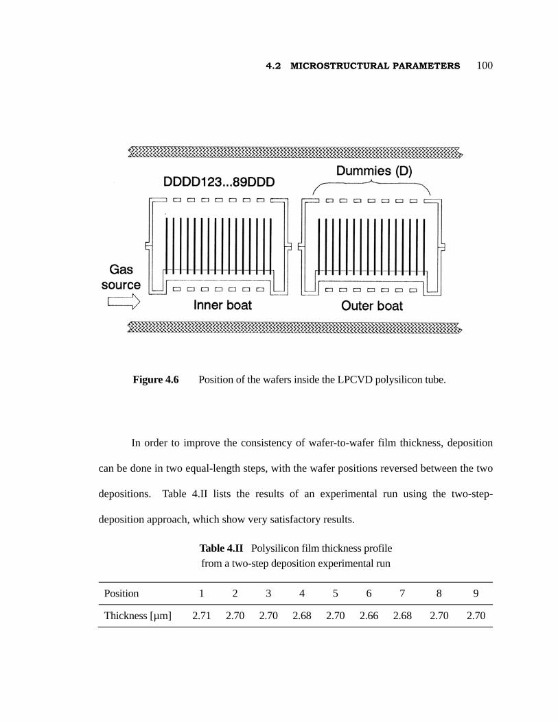
4.2 MICROSTRUCTURAL PARAMETERS 100
In order to improve the consistency of wafer-to-wafer film thickness, deposition
can be done in two equal-length steps, with the wafer positions reversed between the two
depositions. Table 4.II lists the results of an experimental run using the two-step-
deposition approach, which show very satisfactory results.
Table 4.II Polysilicon film thickness profile from a two-step deposition experimental run
Position 1 2 3 4 5 6 7 8 9
Thickness [µm] 2.71 2.70 2.70 2.68 2.70 2.66 2.68 2.70 2.70
Figure 4.6 Position of the wafers inside the LPCVD polysilicon tube.

4.2 MICROSTRUCTURAL PARAMETERS 101
Another alternative is to modify the furnace tube such that reactive gases are distributed
with an injector throughout the length of the furnace.
4.2.2 Plasma-Etching Results
The sidewall profiles of the structural-polysilicon film after reactive-ion etched in CCl4-
O2 plasma depend on, among others factors, the erosion rate of the photoresist mask and
the vertical kinetic energy of the reactive ions [71]. If the photoresist mask is being
continuously eroded away during etching, the sidewall will be angled even when etching
is anisotropic. To slow down mask erosion during etch, selectivity of etching polysilicon
with respect to the photoresist must be increased. This is usually accomplished by
hardening the photoresist mask or by etching at a low ion energy level. However, low-
energy etching results in less anisotropicity, which leads to excessive undercutting of the
polysilicon material. Therefore, the reactive energy must be characterized carefully.
Figure 4.7 is an SEM of a microstructure etched with excessive energy, causing
the top edges to be rounded. Figure 4.8 is an SEM of another structure showing
excessive undercutting, a result of low-energy etch. An optimally etched structure is
shown in Fig. 4.9, which has slightly sloped but straight sidewalls. The optimized recipe
is detailed in Appendix A.
Etch uniformity across a wafer is mostly a function of the reactor geometry and
therefore hard to control. The center of a wafer is usually etched faster because it is in
the center of the plasma discharge and is nearest to the gas sources. Etch nonuniformity
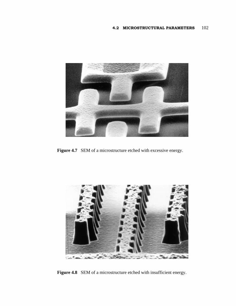
4.2 MICROSTRUCTURAL PARAMETERS 102
placehold placehold placehold placehold placehold placehold placehold placehold
placehold.
Figure 4.7 SEM of a microstructure etched with excessive energy.
Figure 4.8 SEM of a microstructure etched with insufficient energy.

4.2 MICROSTRUCTURAL PARAMETERS 103
placehold placehold placehold placehold placehold placehold placehold placehold
placehold placehold placehold placehold placehold placehold placehold placehold
placehold placehold placehold placehold placehold placehold placehold placehold
placehold
is evidenced by the fact that the resonant frequencies of the same prototype resonators at
the center of the wafer are lower than those near the edge. This is due to narrowed
supporting beams as a result of excessive undercutting near the center of the wafer. The
difference can be as much as 20% in the worst case. By decreasing the etch power and
increasing the amount of overetch, uniformity could be slightly improved, at the expense
of losing anisotropicity. The use of non-erodible mask may also improve the uniformity.
Figure 4.9 SEM of a microstructure etched with optimum energy.

104
4.3 LATERAL-MODE MEASUREMENTS
Two series of lateral-resonator prototypes with different electrostatic comb designs (type
A and type B) are used to verify the stress-relieving property of the folded-beam support
and to evaluate the Young's modulus of the polysilicon film used. The features of these
two types are tabulated in Table 4.III. Each series consists of resonant structures with
beam length from 80 to 200 µm. The different comb-structure dimensions are illustrated
in Fig. 4.10.
Figure 4.10 Comb-structure dimensions.

4.3 LATERAL-MODE MEASUREMENTS 105
Table 4.III Comb drive features of types A and B, with comb width = 4 µm, length = 40 µm, overlap = 20 µm
Type Number of fingers
Finger gap [µm]
Plate mass, Mp [×10–12 kg]
Truss mass, Mt [× 10–12 kg]
A 9 3 35.88 4.23
B 11 2 39.93 4.23
The spring constant, xk , of each structure is calculated with Eqs. (2.45) and
(2.49), with the given beam length and the following beam cross-section dimensions
obtained with the Vickers line-width measurement system on the tested die:
top width, a = 1.95 µm and bottom width, b = 2.05 µm.
The polysilicon film thickness is measured with the Alpha-Step surface profiler, and is
found to be 2.05 µm. The resonant frequencies can then be calculated from Eq. (2.71)
(see section 2.3.1.3 of Chapter 2), using a value of 2.3 × 10³ kg·m–3 for ρ, the density of
polysilicon.
In addition, two torsional structures, one supported with two, two-turn
Archimedean spirals and the other with four serpentine springs which are included in the
same (first) process run. These are tested to verify the differential-drive technique as well
as the rotational stability of the angular vibrations.
The spring constant for the spiral is calculated from Eq. (2.75), while that for the
serpent is obtained with finite-element simulations. Eqs. (2.76) and (2.77) are then used
to evaluate the torsional resonant frequencies (section 2.3.2.3 of Chapter 2).
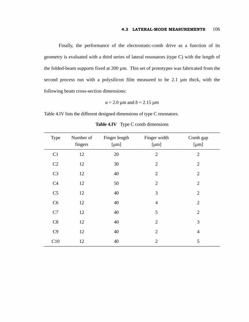
4.3 LATERAL-MODE MEASUREMENTS 106
Finally, the performance of the electrostatic-comb drive as a function of its
geometry is evaluated with a third series of lateral resonators (type C) with the length of
the folded-beam supports fixed at 200 µm. This set of prototypes was fabricated from the
second process run with a polysilicon film measured to be 2.1 µm thick, with the
following beam cross-section dimensions:
a = 2.0 µm and b = 2.15 µm
Table 4.IV lists the different designed dimensions of type C resonators.
Table 4.IV Type C comb dimensions
Type Number of fingers
Finger length [µm]
Finger width [µm]
Comb gap [µm]
C1 12 20 2 2
C2 12 30 2 2
C3 12 40 2 2
C4 12 50 2 2
C5 12 40 3 2
C6 12 40 4 2
C7 12 40 5 2
C8 12 40 2 3
C9 12 40 2 4
C10 12 40 2 5

4.3 LATERAL-MODE MEASUREMENTS 107
4.3.1 Resonant Frequencies and Young’s Modulus
The measured resonant frequencies for types A and B linear resonators are listed in Table
4.V and those for the torsional structures are listed in Table 4.VI. The predicted resonant
frequencies in Tables 4.V and 4.VI are found from Eqs. (2.71) and (2.76) of Chapter 2
with the Young’s modulus E adjusted to give the best fit to the experimental data. From
this first process run, E is found to be 140 GPa.
Table 4.V Predicted and measured resonant frequencies of prototypes A and B
Type A Type B
Beam Length [µm]
Predicted [kHz]
Measured [kHz]
Predicted [kHz]
Measured [kHz]
80 75.5 75.0 ± 0.05 71.8 72.3 ± 0.05
100 53.7 54.3 ± 0.05 51.1 50.8 ± 0.05
120 40.6 41.1 ± 0.1 38.7 39.4 ± 0.1
140 32.0 32.0 ± 0.2 30.5 30.0 ± 0.2
160 26.0 25.9 ± 0.2 24.8 25.0 ± 0.2
180 21.7 21.5 ± 0.3 20.7 20.3 ± 0.3
200 18.4 18.2 ± 0.3 17.6 17.5 ± 0.3
Table 4.VI Predicted and measured resonant frequencies of the torsional structures
Supporting Beam Type
Predicted [kHz]
Measured [kHz]
Spiral 10.5 9.7 ± 0.3
Serpent 60.7 59.4 ± 0.2

4.3 LATERAL-MODE MEASUREMENTS 108
In order to verify the visual-observation results, three different test approaches are
used to obtain the resonant frequencies for the C-series prototypes: visual testing with
continuous-optical illumination, observation with strobe light, and electrical testing with
modulation technique. The results are listed in Table 4.VII., which shows that the results
obtained from the three testing methods independently agree with the calculated results.
Table 4.VII Predicted and measured resonant frequencies of the C-series prototypes
Measured
Type Calculated Optical ± 0.05
Strobe ± 0.05
Electrical ± 0.05
C1 23.4 22.9 23.1 22.8
C2 22.6 22.3 22.4 22.9
C3 21.9 22.1 22.0 22.0
C4 21.3 21.5 21.6 21.6
C5 20.4 20.9 20.5 20.3
C6 19.1 19.2 19.3 19.3
C7 18.1 18.8 18.4 18.0
C8 21.3 21.1 21.2 21.4
C9 20.8 20.5 20.7 21.0
C10 20.2 20.0 19.9 19.8
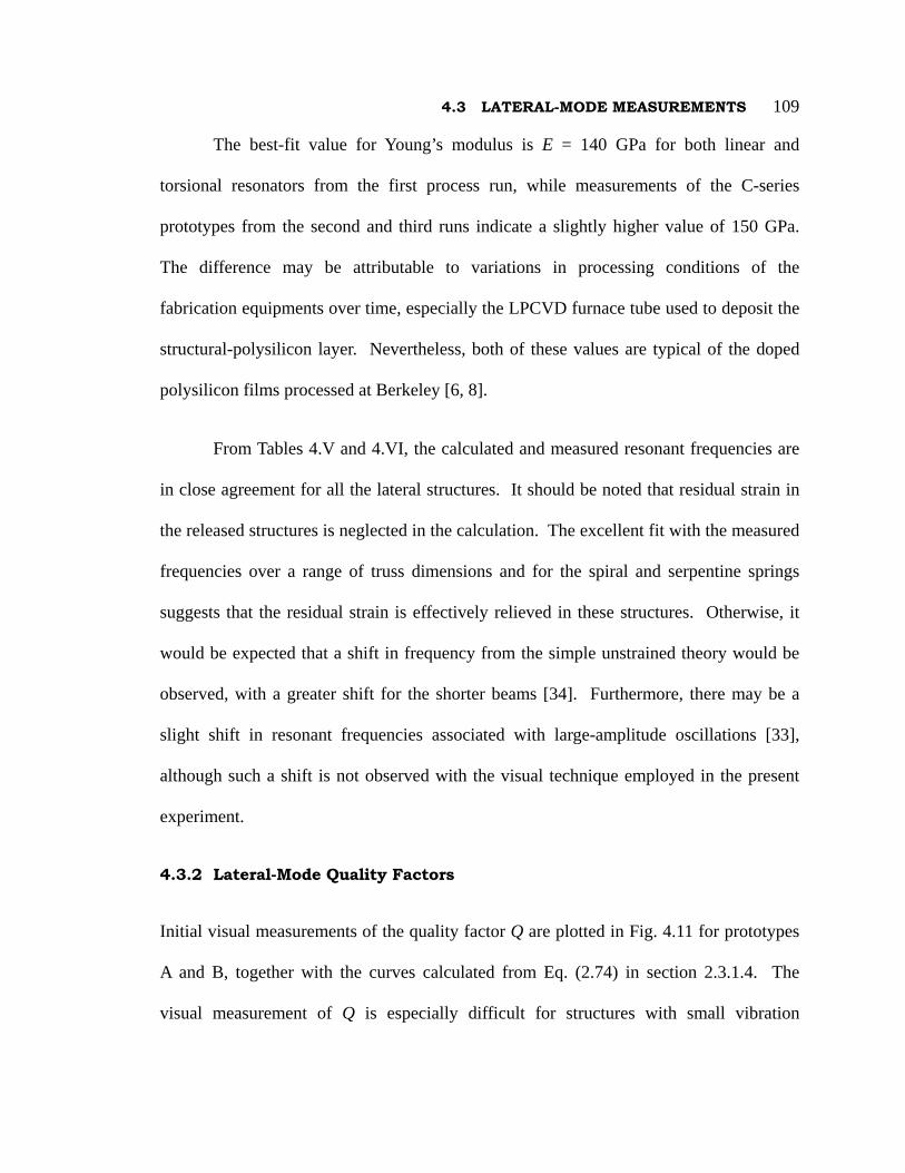
4.3 LATERAL-MODE MEASUREMENTS 109
The best-fit value for Young’s modulus is E = 140 GPa for both linear and
torsional resonators from the first process run, while measurements of the C-series
prototypes from the second and third runs indicate a slightly higher value of 150 GPa.
The difference may be attributable to variations in processing conditions of the
fabrication equipments over time, especially the LPCVD furnace tube used to deposit the
structural-polysilicon layer. Nevertheless, both of these values are typical of the doped
polysilicon films processed at Berkeley [6, 8].
From Tables 4.V and 4.VI, the calculated and measured resonant frequencies are
in close agreement for all the lateral structures. It should be noted that residual strain in
the released structures is neglected in the calculation. The excellent fit with the measured
frequencies over a range of truss dimensions and for the spiral and serpentine springs
suggests that the residual strain is effectively relieved in these structures. Otherwise, it
would be expected that a shift in frequency from the simple unstrained theory would be
observed, with a greater shift for the shorter beams [34]. Furthermore, there may be a
slight shift in resonant frequencies associated with large-amplitude oscillations [33],
although such a shift is not observed with the visual technique employed in the present
experiment.
4.3.2 Lateral-Mode Quality Factors
Initial visual measurements of the quality factor Q are plotted in Fig. 4.11 for prototypes
A and B, together with the curves calculated from Eq. (2.74) in section 2.3.1.4. The
visual measurement of Q is especially difficult for structures with small vibration
4.3 LATERAL-MODE MEASUREMENTS 110
placehold placehold placehold placehold placehold placehold placehold placehold
placehold
Figure 4.11 Measured and calculated Q vs. beam length.

4.3 LATERAL-MODE MEASUREMENTS 111
amplitudes, which is reflected in the larger error bars for these points. The calculated
quality factors are consistently higher than the measured values, indicating that the
assumption of including only Couette flow underneath the plate in evaluating Q is an
oversimplification for these structures. However, the calculated values of Q are within a
factor of two of the actual measurements and may be useful for design purposes. The
highest measured Q is about 130 for a structure with 80 µm-long folded-beam suspension.
In order to study the contribution of the comb-finger damping to the quality
factor, the C-series prototypes are tested for Q with all three testing methods. The gap
between comb fingers is found to be the most important design parameter for the quality
factor. Figure 4.12 is a plot of the optical and electrical measurements of the quality
factor Q for the set of test structures with different finger gaps (prototypes C3, C8–C10).
An important observation from Fig. 4.12 is that Q is low for structures with either small
finger gaps or widely separated fingers. Tightly spaced fingers lead to higher air-drag
damping, while widely spaced ones must be attached to a wider structure for support, and
hence also resulting in more air damping.
In order to evaluate the quality factor of the resonator in vacuum, one of the type
A linear resonators with 140 µm-long folded-beam support is packaged and tested inside
an SEM at a pressure of 10–7 torr. Figure 4.13 is an SEM of the vibrating structure
driven by a 100 mV-amplitude ac voltage on top of a 5 V dc bias. The vibration
amplitude is estimated to be 10 µm peak-to-peak. In the SEM, this structure resonates
at rf = 31,636.91 ± 0.02 Hz. The quality factor is evaluated with both time- and

4.3 LATERAL-MODE MEASUREMENTS 112
placehold placehold placehold placehold placehold placehold placehold placehold
placehold
Figure 4.12 Q vs. finger gap.

4.3 LATERAL-MODE MEASUREMENTS 113
placehold placehold placehold placehold placehold placehold placehold placehold
placehold placehold placehold placehold placehold placehold placehold placehold
placehold placehold placehold placehold placehold placehold placehold placehold
placehold placehold placehold placehold placehold placehold placehold placehold
placehold placehold placehold placehold placehold placehold placehold placehold
placehold placehold placehold placehold placehold placehold placehold placehold
placehold placehold placehold placehold placehold placehold placehold placehold
frequency-domain methods:
rr
2 11.43 and fQ Tf Q
f f≈ =
− (4.3)
where T is the time for the oscillation amplitude to drop from 90% to 10% of its full
amplitude after stopping the drive, and ( 2 1f f− ) is the –3 dB bandwidth (Fig. 4.14). The
values of Q are 49,000 ± 2,000 and 50,000 ± 5,000 from the time- and frequency-domain
methods, respectively.
The vibration of the structure is lateral to the substrate, without any indication of
placehold placehold ehold placehold placehold placehold placehold placehold placehold
Figure 4.13 SEM of a vibrating structure under high vacuum (10–7 torr).

4.3 LATERAL-MODE MEASUREMENTS 114
placehold placehold placehold placehold placehold placehold placehold placehold
placehold
Figure 4.14 Time- and frequency-domain methods for Q evaluation.

4.3 LATERAL-MODE MEASUREMENTS 115
torsional or vertical motion. It is important to note that the mechanical resonant frequency
of the vertical mode is very close to that of the designed lateral mode due to the almost
square cross section of the suspensions. A purely lateral vibration is excited as a result of
the shift in the vertical resonant frequency due to the unbalanced comb drive (see section
2.2 of Chapter 2).
4.3.3 Capacitance Gradient, ∂C/∂x
With the value of Q measured and the spring constant kx established, we need only to
measure the electromechanical transfer function at resonance to evaluate ∂C/∂x with Eq.
(2.11) of Chapter 2. Alternatively, we can measure the static displacement of the
structure under a dc bias, and use the solution of Eq. (2.5) to calculate ∂C/∂x, without
having to know Q a priori.
Figure 4.15 is a comparison of the experimental results for prototypes A and B with
the calculated values from Eq. (2.11), for which ∂C/∂x for the two types of comb drives is a
fitting parameter. The type A drive is found to have ∂C/∂x = 58 aF·µm–1 and type B has
∂C/∂x = 150 aF·µm–1.
The C-series prototypes are used to study the effects of different comb designs on
∂C/∂x. It is found that the comb gap has the most effect on the values of ∂C/∂x. Figure
4.16 is a plot of ∂C/∂x as a function of the finger gap, which shows the expected sharp
increase with reduced gaps. Both Figs. 4.12 and 4.16 indicate that the three different
measurement techniques are in good agreement within experimental errors. These two

4.3 LATERAL-MODE MEASUREMENTS 116
placehold placehold placehold placehold placehold placehold placehold placehold
placehold
Figure 4.15 Measured and calculated values of the transfer functions.

4.3 LATERAL-MODE MEASUREMENTS 117
Figure 4.16 ∂C/∂x vs. finger gap.

4.3 LATERAL-MODE MEASUREMENTS 118
plots also provide the empirical basis for designing electrostatic-comb drive.

119
4.4 VERTICAL-MODE MEASUREMENTS
Prototypes from the third process run (V-series) are used to study vertical-mode
excitation. They are designed with 400 µm-long folded-beam supports to provide
compliance in both the out-of-plane (z) and the lateral (x) directions. The polysilicon-
film thickness of the device under test is measured to be 1.94 µm with Alpha-Step. The
cross-sectional dimensions are a = 2.2 µm and b = 2.8 µm from Vickers linewidth
measurements. These dimensions are somewhat wider than the designed 2 µm due to a
combination of slight underexposure and underdevelopment on the photoresist. Note also
that the sidewalls from this process run are more angled than that from the first and
second run, due to the change of the photolithography system. The new photoresist
(Olin-Hunt 6512, I-line resolution) that is used in this run erodes slightly faster than the
original KTI 820 G-line resist under the same etching conditions and parameters in CCl4-
O2 plasma.
The comb drives of all V-series prototypes have lateral vernier scales to measure
lateral deflections. The structures are first resonated laterally to evaluate the Young’s
Modulus from the measured resonant frequencies, using Eqs. (2.45), (2.49) and (2.71)
from sections 2.3.1.1 and 2.3.1.3 of Chapter 2. The same value for the Young's modulus
is then used for the vertical-motion calculations based on the fact that polysilicon is
materially isotropic.
The value for the Young’s modulus is found to be 150 GPa, similar to the value
found from the second process run but slightly higher than the 140 GPa value from the
placehold placehold placehold placehold placehold

4.4 VERTICAL-MODE MEASUREMENTS 120
first run. The lateral spring constant is then calculated to be
( )( )2 2x 32
hk a b a b EL
= + + =140 nN·µm–1 (4.4)
Similarly, the vertical spring constant is evaluated as
( )
( )
3 2 2
z 3
2 4
3
h a ab bk E
L a b
+ += =
+86 nN·µm–1 (4.5)
Vertical motions are tested entirely in a low-voltage (1.6 kV) SEM to minimize
charging effects due to the scanning-electron beams. All structures are wired together to
make possible the measurement of a number of structures in a single SEM session. The
angle of tilt of the sample inside the SEM chamber and the magnification are fixed for
comparison between different structures. Vertical displacements are evaluated by
accurately measuring the SEM images with a set of standard linewidths.
The comb dimensions for all the V-series prototypes are nominally 40 µm long, 4
µm wide, with a gap of 2 µm. However, underetch is evidenced by the cross-sectional
dimension of the supporting beam, and thus 0.1 µm and 0.3 µm are added to all top and
bottom perimeters, respectively. The structures are offset from the substrate by 2.0 µm.
The different interdigitation designs in the V series are listed in Table 4.VIII. Figures
4.17–4.19 are the optical micrographs of some of the comb designs.
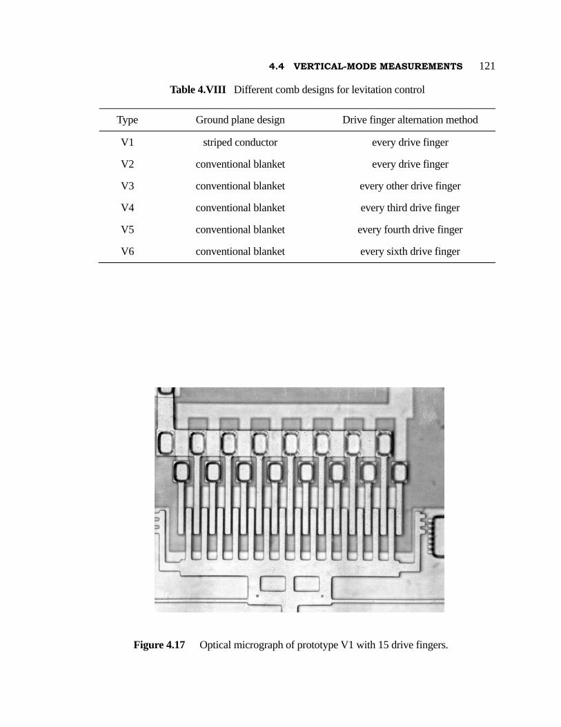
4.4 VERTICAL-MODE MEASUREMENTS 121
Table 4.VIII Different comb designs for levitation control
Type Ground plane design Drive finger alternation method
V1 striped conductor every drive finger
V2 conventional blanket every drive finger
V3 conventional blanket every other drive finger
V4 conventional blanket every third drive finger
V5 conventional blanket every fourth drive finger
V6 conventional blanket every sixth drive finger
Figure 4.17 Optical micrograph of prototype V1 with 15 drive fingers.

4.4 VERTICAL-MODE MEASUREMENTS 122
Figure 4.18 Optical micrograph of prototype V2 with 13 drive fingers.
Figure 4.19 Optical micrograph of prototype V4 with 12 drive fingers.

4.4 VERTICAL-MODE MEASUREMENTS 123
The following presents the comparison of the effectiveness of different designs
after an evaluation of the levitation phenomenon.
4.4.1 DC Levitation Results
Levitation is first measured by applying a voltage of 0 to 25 V to all drive fingers on one
of the V1 prototypes with 18 movable comb fingers and 19 fixed drive fingers, the result
of which is plotted in Fig. 4.20. Figure 4.21 is an SEM of a V2 prototype levitated under
a 10 V dc bias. The vertical displacement increases with applied voltage and reaches an
equilibrium near 20 V where the attractive forces between the displaced interdigitated
fingers offset the repulsive electrostatic forces between the ground plane and movable
fingers (see section 2.2 of Chapter 2). The initial negative deflection for a grounded
comb, shown in Fig. 4.20, cannot be attributed to gravity. Charging effects in the
exposed underlying dielectric films between the interdigitated striped ground plane are a
likely source of this offset displacement. To account for the initial negative deflection,
we hypothesize a fixed-charge force, cF , which attracts the structure to the substrate:
( )c 2Fz dβ=+
(4.6)
where d is the nominal offset of the structure from the substrate and β is the constant of
proportionality. Figure 4.22 illustrates the addition of cF to the system. The term cF is
now added to Eq. (2.23) of section 2.2.3 of Chapter 2 as
net z k c 0F F F F= − − = (4.7)
Equations (2.21) and (2.24) of section 2.2.3 are combined with Eq. (4.6) to substitute the
placehold placehold

4.4 VERTICAL-MODE MEASUREMENTS 124
Figure 4.20 Levitation as a result of a common voltage applied to all electrodes.
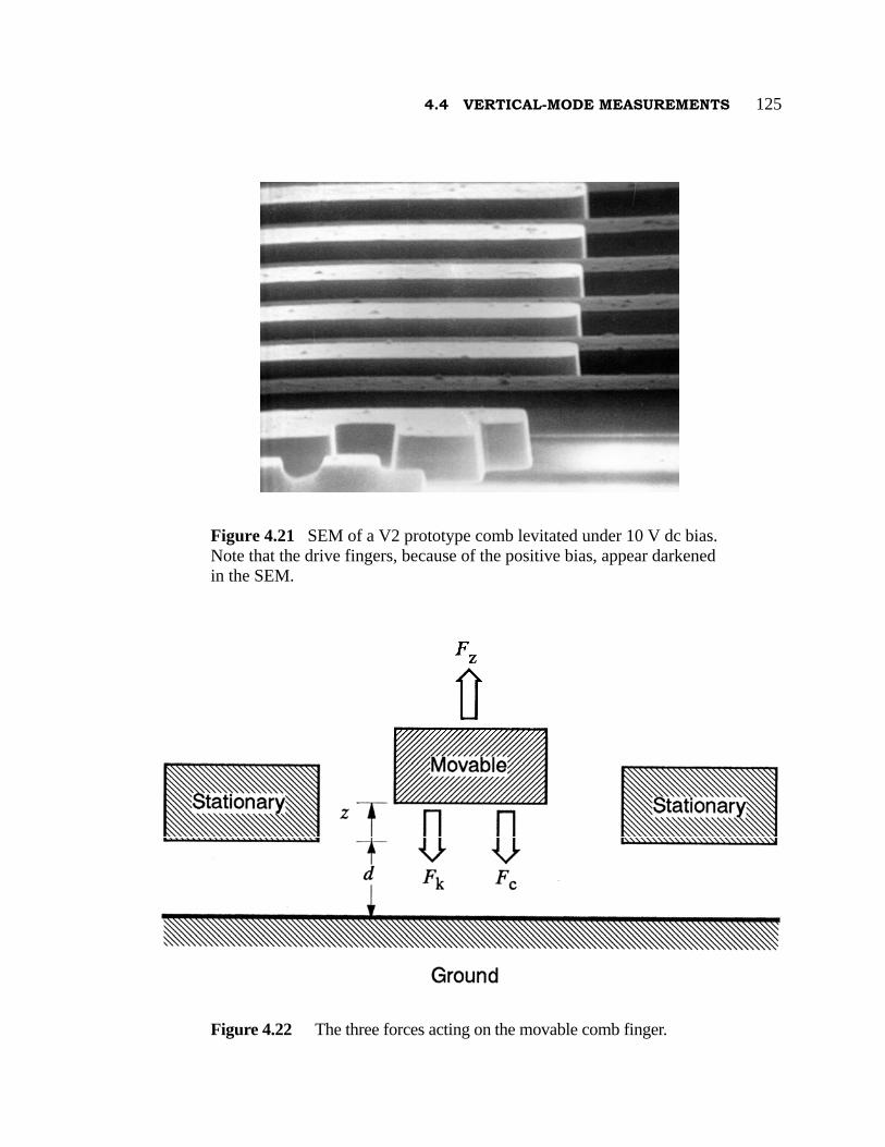
4.4 VERTICAL-MODE MEASUREMENTS 125
Figure 4.21 SEM of a V2 prototype comb levitated under 10 V dc bias. Note that the drive fingers, because of the positive bias, appear darkened in the SEM.
Figure 4.22 The three forces acting on the movable comb finger.

4.4 VERTICAL-MODE MEASUREMENTS 126
terms in Eq. (4.7), yielding an implicit function as follows
( )( )
12 2
zP
z 0 0
//
k z z dV
z z zβ
γ
⎛ ⎞+ +⎜ ⎟=⎜ ⎟−⎝ ⎠
(4.8)
Figure 4.23 is the result of fitting the curve to the data in Fig. 4.20 by adjusting
0z , zγ and β. The best-fitted values are 0z = 400 nm, zγ = 47 pN·V–2 per drive finger,
and β = 23.6 nN·µm2. The equilibrium levitation ( 0z ) of 0.4 µm is much less than the
observed 2 µm levitation in some structures with soft spring supports and a blanket
ground plane.
The effectiveness of levitation control by alternating the potentials on every drive
finger of prototype V1 is evaluated next. Figure 4.24 is a plot of the measured vertical
displacement resulting from holding one set of an alternating drive fingers at +15 V and
varying the other set of electrodes from –15 V to +15 V. This structure is the same as that
tested in Fig. 4.20. As expected, negative voltages in the range of –10 V to –15 V
suppress the lifting behavior. As the disparity between the magnitudes of the voltages
increases, more lifting occurs, with the limiting case of +15 V applied to all drive fingers
yielding the same vertical displacement as found in Fig. 4.20. Figure 4.25 is the SEM of
prototype V1 under a ±10 V balanced biasing on the alternating drive fingers, indicating
almost no levitation. Note that the voltage-contrast effect inside the SEM causes the
drive fingers at a higher potential to appear darkened.

4.4 VERTICAL-MODE MEASUREMENTS 127
Figure 4.23 Measured and calculated levitation for prototype V1.

4.4 VERTICAL-MODE MEASUREMENTS 128
Figure 4.24 Vertical displacement of prototype V1 for varying voltage on one electrode from -15 V to +15 V, while holding the other electrode fixed at +15 V.

4.4 VERTICAL-MODE MEASUREMENTS 129
4.4.2 Vertical and Lateral Drive Capacities
It is found that, besides suppressing the vertical levitation, the balanced-biasing approach
on the alternating drive fingers induces a weaker lateral force on the structure than the
unbalanced comb. The balanced comb is advantageous only if the tradeoff between
levitation suppression and loss of lateral drive is favorable. In order to quantify the
comparison of the lateral and vertical force reductions, we define the lateral drive
capacity, xγ , of an electrostatic-comb drive as the lateral force induced per square of the
placehold placehold placehold placehold placehold placehold placehold placehold
Figure 4.25 SEM of prototype V1 under ±10 V balanced biasing on the alternating drive fingers, indicating almost no levitation. Fingers at higher potentials appear darkened due to voltage-contrast effect in SEM.

4.4 VERTICAL-MODE MEASUREMENTS 130
applied voltage:
xx 2
P
FV
γ = [pN·V–2] (4.9)
The value of xγ is normalized to each drive finger, and is found to be 16 ± 1 pN·V–2 per
drive finger for all the unbalanced comb designs. Both zγ and xγ for the V-series
prototypes are tabulated in Table 4.IX. The reductions in γ are defined as the ratios of the
drive capacities of the unbalanced comb to those of the balanced one.
Table 4.IX Normalized zγ and xγ per drive finger for V-series prototypes
Type zγ at z = 0
± 1 pN·V–2
xγ
± 1 pN·V–2
zγ
reduction
xγ
reduction
Unbalanced 47 16 - -
V1 3 10 16:1 1.6:1
V2 26 8 1.8:1 2:1
V3 30 11 1.6:1 1.5:1
V4 35 12 1.3:1 1.3:1
V5 36 14 1.3:1 1.1:1
V6 38 14 1.2:1 1.1:1
Although none of the comb designs completely eliminates the levitation as
predicted by idealized theory, which assumes evenly spaced comb fingers with vertical
sidewalls, the V1 prototype stands out as the best approach, with a 16:1 reduction on the
vertical drive capacity while suffering only a 1.6:1 reduction in induced lateral force. All
of the other interdigitation methods are ineffective.

4.4 VERTICAL-MODE MEASUREMENTS 131
4.4.3 Vertical Resonant Frequencies
The vertical resonant frequencies for prototype V1 are found by stepping the output
frequency of an HP 4192A LF Impedance Analyzer at 0.1 Hz steps at different dc biases
from 5.0 V to 15.0 V, and fixing the ac drive amplitude at 50 mV. Figure 4.26 is the SEM
of prototype V1 driven into vertical resonance. The vibration amplitude is estimated to
be 2 µm peak-to-peak. The results are plotted in Fig. 4.27, with the theoretical curve
fitted to the data with 0z and zγ adjusted to 400 nm and 47 pN·V–2, respectively.
Figure 4.26 SEM of prototype V1 driven into vertical resonance under
a 50 mV ac drive on top of a 5 V dc bias.
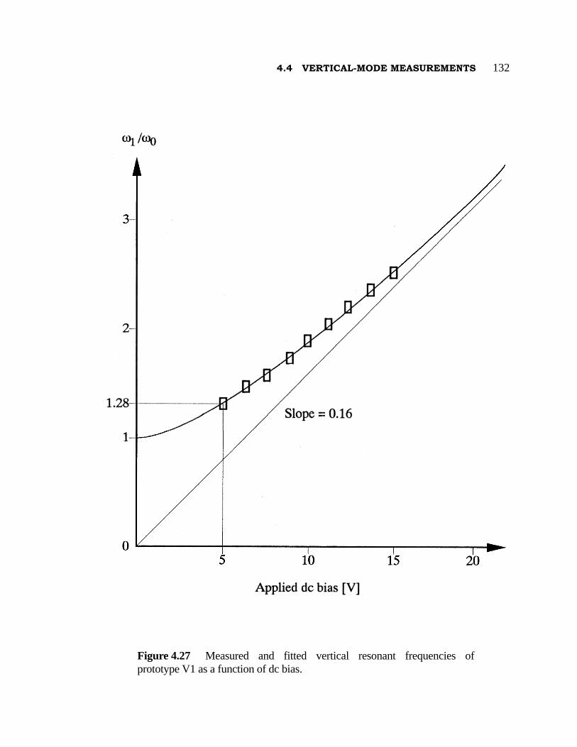
4.4 VERTICAL-MODE MEASUREMENTS 132
Figure 4.27 Measured and fitted vertical resonant frequencies of
prototype V1 as a function of dc bias.
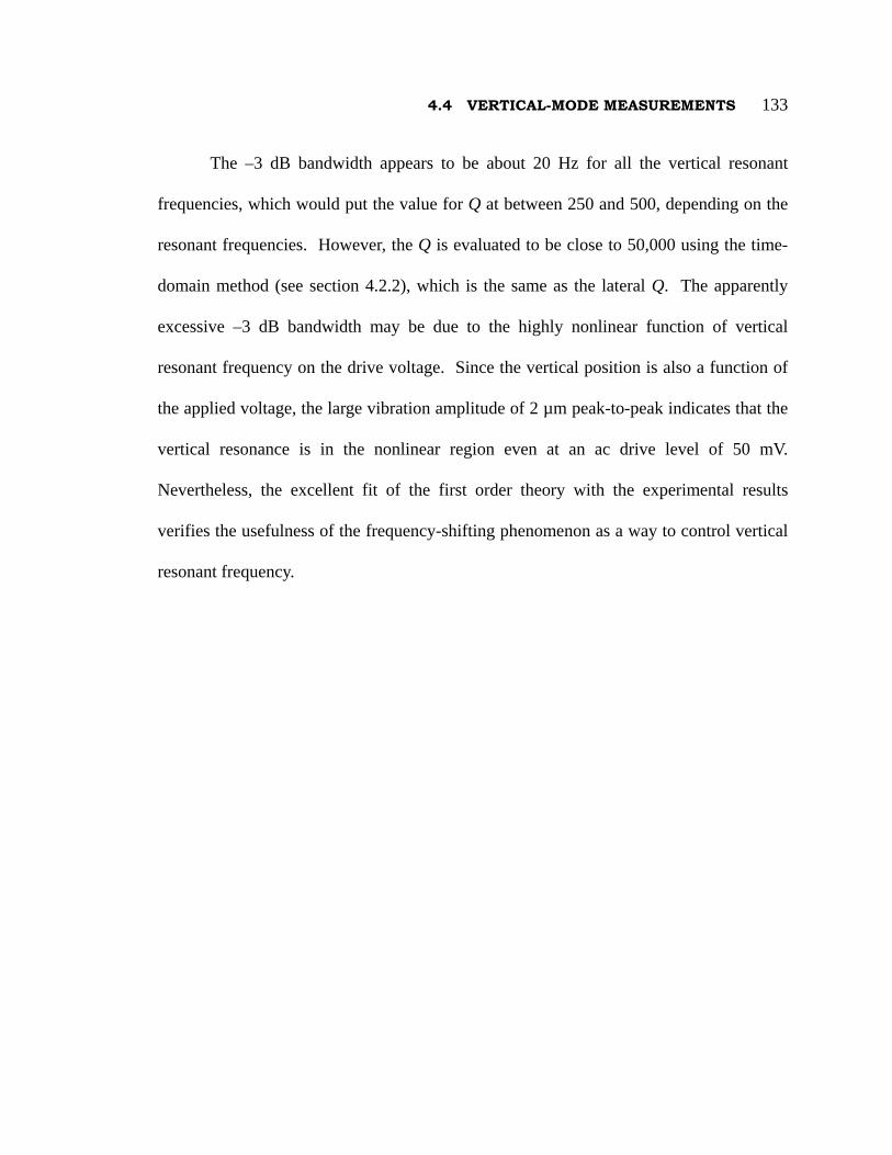
4.4 VERTICAL-MODE MEASUREMENTS 133
The –3 dB bandwidth appears to be about 20 Hz for all the vertical resonant
frequencies, which would put the value for Q at between 250 and 500, depending on the
resonant frequencies. However, the Q is evaluated to be close to 50,000 using the time-
domain method (see section 4.2.2), which is the same as the lateral Q. The apparently
excessive –3 dB bandwidth may be due to the highly nonlinear function of vertical
resonant frequency on the drive voltage. Since the vertical position is also a function of
the applied voltage, the large vibration amplitude of 2 µm peak-to-peak indicates that the
vertical resonance is in the nonlinear region even at an ac drive level of 50 mV.
Nevertheless, the excellent fit of the first order theory with the experimental results
verifies the usefulness of the frequency-shifting phenomenon as a way to control vertical
resonant frequency.

134
4.5 SUMMARY
In this chapter we have presented the measurement techniques and have analyzed the
static and dynamic characteristics of both the lateral and vertical modes of operations.
The large-amplitude resonance, which is characteristic of the electrostatic comb drive
with the folded-beam suspension, enables straightforward measurements of the motions
by direct observations with either optical microscope or SEM. The modulation-based
testing technique provides an electrical verification of the observed measurements.
Although the nonuniform thickness and built-in stress of the deposited polysilicon film
and the less-than-ideal plasma etching step affect the characteristics of the finished
structures slightly, the basic functional advantages of the comb-drive structure such as
large vibration amplitude, linearity, and the ability to control vertical motions are
realized. The robustness of the laterally-driven microstructures is further demonstrated
by the excellent fit of the first-order theories with the measurement results for both lateral
and vertical modes of operation.

135
Chapter 5
ACTUATOR APPLICATION EXAMPLE
In the previous chapters, we have established the first-order theory, described the
processing techniques and compared the experimental and theoretical results of the lateral
and vertical modes of motion of the electrostatic-comb structures. This chapter describes
the design and theory of a two-dimensional manipulator as an example of applying the
comb drive as an actuating element. The manipulator can be used potentially to improve
the performance of a resonant micromotor. The structure can be analyzed with an
approach similar to that developed in Chapter 2 and fabricated with the same surface-
micromachining technique described in Chapter 3.
5.1 TWO-DIMENSIONAL MANIPULATOR
In robotics system applications, complicated multidimensional motions are usually
achieved by mechanically coupling an array of one-dimensional actuators capable of
performing periodic rotary or linear motions. Stepper motors and electromagnetic
resonators are common examples of one-dimensional periodic actuators.
One of the simplest forms of actuator coupling based on the electrostatic-comb
drive is illustrated in Fig. 5.1, which shows the basic design of an orthogonally coupled
placehold.

5.1 TWO-DIMENSIONAL MANIPULATOR 136
Figure 5.1 Basic design of an orthogonally coupled comb-drive pair to form a two-dimensional manipulator.

5.1 TWO-DIMENSIONAL MANIPULATOR 137
comb-drive pair to form a two-dimensional manipulator. The combs are resonated by
sinewave signals at 90°-phase difference to achieve circular or elliptical motions on the
pawl tip. If the lateral-drive capacities of the combs are sufficiently high to statically
deflect the suspensions, then any arbitrary motions can be obtained by independently
driving the combs at off-resonant, low-frequency modes.

138
5.2 RESONANT MICROMOTOR APPLICATION
The two-dimensional manipulator can be far more versatile than a single comb-drive
resonator in many applications. An example is the resonant-structure micromotor
concept briefly described in Section 2.2 of Chapter 2. The original suggested micromotor
is based on a tuning-fork actuating element, where the vibration energy is used to turn a
gear wheel with a ratchet-and-pawl mechanism (Fig. 5.2) [30]. This concept can be
implemented using a comb drive as the actuator as illustrated in Fig. 5.3.
A critical design issue is the interaction between the pawl tip and the gear tooth,
where tooth interference and friction must be considered carefully [72]. Figure 5.4 is the
close-up view of the pawl tip and the gear wheel in resting position. When the vibration
of the pawl builds up to a sufficient amplitude to push forward the gear wheel, the
subsequent tooth will move into a position where the pawl motion is interfered, as
illustrated in Fig. 5.5. The frictional force between the pawl and the tooth, if sufficiently
large, may drag the wheel in the backward direction when the pawl retracts. One or more
passive ratchets are usually placed along the perimeter of the wheel to prevent backward
motion. However, excessive friction between the gear teeth and the pawls and ratchets
may prove fatal to the micromotor.
In order to reduce friction and to eliminate the need for passive ratchets, it is
desirable to engage the gear wheel with elliptical pawl tip motions (Fig. 5.6). To further
reduce the stress on the hub, two pawls can be used on the opposite sides of the wheel to
eliminate translational force at the center of the wheel.

5.2 RESONANT MICROMOTOR APPLICATION 139
Figure 5.2 Resonant-structure micromotor concept [30].

5.2 RESONANT MICROMOTOR APPLICATION 140
Figure 5.3 Resonant micromotor implemented with the comb drive as the actuating element.
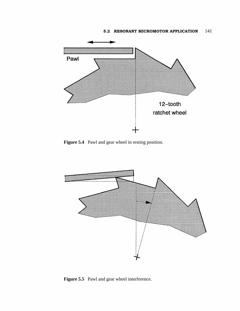
5.2 RESONANT MICROMOTOR APPLICATION 141
Figure 5.4 Pawl and gear wheel in resting position.
Figure 5.5 Pawl and gear wheel interference.

5.2 RESONANT MICROMOTOR APPLICATION 142
Figure 5.6 Improved pawl-ratchet engagement with elliptical pawl motions.

143
5.3 STABILITY AND DESIGN CONSIDERATIONS
Operation of the two-dimensional manipulator requires that the coupled pawls are
compliant in sideways motion to avoid inducing excessive sideways force on the comb
drive. The simulation results of the spring constants of serpentine-spring supports
described in Section 2.3.2.2 of Chapter 2 can be used as a design guideline for the
coupled pawls. Figure 5.7 is the redesigned gear wheel with a pair of orthogonally
coupled serpentine springs as flexible pawls. Note that square teeth are used instead of
saw teeth such that the gear wheel can be turned in either directions. In this case, push-
placehold.
Figure 5.7 Modified resonant micromotor with differential elliptical drives.

5.3 STABILITY AND DESIGN CONSIDERATIONS 144
pull drives are needed for the pawls.
In order to provide push-pull capability and increased lateral drive capacity for
off-resonant operation, the comb-drive structure is modified as shown in Fig. 5.8.
Alternating drive fingers are employed in the design to minimize the effect of levitation.
A single-folded supporting beam is used instead of the more compact double-folded one
to obtain better lateral stiffness.
As an example, Fig. 5.9 is the simulated mode shape of an orthogonally coupled
pawl when a force is induced on the x-axis actuator. The dimensions of each of the
serpentine spring in this example are (see Section 2.3.2.2 of Chapter 2)
m 8N = , m 8W = µm, and beam cross section = 2 µm × 2 µm.
The spring constant for this coupled pawl in the x direction, kx, is simulated to be 619
nN·µm–1, which is more than two-and-a-half times higher than the 233 nN·µm–1 value for
simple bending of a single serpentine pawl with the same dimensions (see Section 2.3.2.2
of Chapter 2). The value for yk , the coupled spring constant in the y direction, is equal to
xk since the two serpentine supports are identically dimensioned. It is desirable for xk to
be as small as possible such that the lateral load on the y-axis actuator is minimized.
Similarly, a small yk minimizes the lateral load on the x-axis actuator. The resonant
frequency for the whole manipulator is calculated from the system spring constant, which
is the sum of the spring constant of the folded-beam support and that of the orthogonally
coupled pawl.
For the particular design illustrated in Fig. 5.8, the orthogonally coupled serpentine
placehold

5.3 STABILITY AND DESIGN CONSIDERATIONS 145
Figure 5.8 Push-pull comb-drive actuator.

5.3 STABILITY AND DESIGN CONSIDERATIONS 146
Figure 5.9 Model shape of an orthogonally couled serpentine spring pair under a force xF .

5.3 STABILITY AND DESIGN CONSIDERATIONS 147
pawl is designed with the following dimensions:
m 33N = , m 8W = µm, and beam cross section = 2 µm × 2 µm.
The simulated spring constant of this design is
x pawl 8.8k = nN·µm–1 (5.1)
The spring constant of the 300 µm-long, one-sided, single-folded spring support is
calculated with Eq. (2.45) (see Section 2.3.1.1 of Chapter 2). Since we now have a one-
sided support, the spring constant is
3
zx 3 3beam
24 892
EI EhwkL L
= = = nN·µm–1 (5.2)
which is more than ten times the value of x pawlk . Given the even higher ratio of y beamk
to x beamk , the sideways bending of the pawl will have negligible effect on the normal
operation of the associated comb drive. The resonant frequency is then calculated with
Eq. (2.71) of Section 2.3.1.3 of Chapter 2, and is found to be 3.82 kHz.
The lateral drive capacity ( xγ ) for the push-pull actuator in Fig. 5.8 is evaluated
to be 0.74 nN·V–2 based on the experimental results described in Chapter 4. Thus, a ±30
V differential bias applied to the two sides of the push-pull comb drive will induce a
static deflection of
( )
2 2x
1beam pawl
2 (30 V) 0.74 nN·V 13.6 µm89 8.8 nN·µmx x
Fxk k
−
−× ×Δ = = =
+ +
which is more than sufficient to statically manipulate the gear wheel.
In order to shed light on the forces between the pawls and the gear teeth, a
placehold.

5.3 STABILITY AND DESIGN CONSIDERATIONS 148
microdynamometer is designed with similar dimensions as the resonant micromotor,
except that the gear wheel is supported by a pair of Archimedean spirals with two needles
added to the perimeter of the wheel to indicate the amount of deflection (Fig. 5.10).
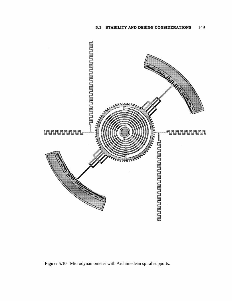
5.3 STABILITY AND DESIGN CONSIDERATIONS 149
Figure 5.10 Microdynamometer with Archimedean spiral supports.
150
5.4 SUMMARY
We have discussed the theory of the two-dimensional manipulator as an extension of the
electrostatic-comb drive to demonstrate possible applications in resonant micromotor and
microdynamometer. The major potential advantage of the proposed manipulator is its
increased versatility without adding processing steps. Initial calculations indicated that it
is feasible to statically move the manipulator pawl tip in any arbitrary large-amplitude
planar motions parallel to the substrate. However, the theory is yet to be verified.

151
Chapter 6
CONCLUSIONS
We conclude the thesis with this final chapter by evaluating the surface-micromachined
electrostatic-comb drive in light of the research goal, which is to establish a foundation
for electrostatically exciting and sensing suspended micromachined transducer elements.
The merits and weaknesses of the lateral-drive approach are evaluated, based on the
potential applications of resonant sensors and actuators for micromechanical systems, and
we point to the direction for future research.
6.1 EVALUATION OF THIN-FILM ELECTROSTATIC-COMB DRIVE
Since tribology at the micron-sized domain is not well understood, the general
development of microactuators is concentrated either in basic research on friction and
other related micromechanical properties, or in frictionless or minimal-friction devices.
The key to the development of a frictionless microstructure is the availability of robust
flexure suspensions that can sustain repetitive cycles of motion in a predetermined
manner. Also, an efficient and compatible periodic energy source is needed for
excitation. We have taken the full advantage of the well-established planar-IC
technology to develop and demonstrate suspended planar micromechanical devices
capable of large-amplitude motions that are driven and sensed electrostatically.

6 CONCLUSIONS 152
LPCVD polycrystalline silicon is chosen as the material for the spring
suspensions and other associated mechanical parts simply because of its mature
micromachining technology. Plasma-etched microstructures are superior in their fracture
toughness because of its ability to disperse stress concentrations due to the absence of
sharply angled corners.
Arbitrary shapes can be easily patterned in one masking step with the lateral-drive
approach. At the minimum, one masking step is sufficient to fabricate functioning
electrostatic-comb drives. The linearity and efficiency of the electrostatic-comb drive have
been shown to be advantageous for microactuator applications. Since the levitation
phenomenon has been sufficiently analyzed and a control method has been experimentally
verified, it can be used as a functioning feature of the electrostatic-comb drive. Finally, a
two-dimensional manipulator design is theoretically feasible as an example of building
geometrically sophisticated planar structures without adding processing steps.
However, the limited thickness of all thin-film processed microstructures, including
the electrostatic-comb drive, may inherently restrict its usefulness in certain applications.
The following section discusses this issue from the perspective of geometrical scaling.

6 CONCLUSIONS 153
6.2 SCALING CONSIDERATION AND ALTERNATIVE PROCESS
As discussed in Section 2.1.2 of Chapter 2, since ∂C/∂x≈2αεhg–β per drive finger, it is
desirable to decrease the finger gap g and increase the thickness h to enhance the drive
efficiency. Also, increased film thickness is advantageous for improving mechanical
stability of the finished structures. However, for a 2 µm-thick polysilicon film,
conventional photolithography and plasma-etching techniques would place a lower limit
on resolving g to probably no less than 1 µm. Also, a near-vertical sidewall would be
more difficult to obtain at decreased gap clearances. To increase h, a thick polysilicon
film can be deposited at the expense of long deposition time and accelerated need for
furnace tube maintenance. However, thicker films are progressively more difficult to
pattern because of the obscured alignment mark, except in the case of the single-mask
process. The use of non-erodible mask would become necessary for the extended
plasma-etch step for thick films. To form the non-erodible mask, a two-step approach is
usually adopted where an intermediate layer of photoresist is first patterned to define the
mask which is then used to pattern the underlying polysilicon film after the photoresist
layer is optionally removed. This two-step approach may degrade the feature resolution,
and thus increasing the minimum resolvable g. Therefore, the processing steps described
in Chapter 3, if not extensively modified, are best suited for film thickness of 4 µm or
less, with a gap clearance of at least 1 µm.
Extending beyond conventional IC technology, recent research has provided
alternatives to create microstructures with high aspect ratios [73–75]. Using deep-etch,
placehold

6 CONCLUSIONS 154
high-energy X-ray lithography with a synchrotron and specialized developer, polymeric
photoresist as thick as 300 µm has been patterned to form the mold for depositing metals
onto the exposed areas of the underlying conductive substrate by electroforming [73].
Minimum separation between structures as small as 3 µm was achieved, with excellent
vertical sidewalls [73]. The use of deep UV source for lithography has also been reported
to obtain structures as thick as 8 µm without the need for synchrotron [74]. If a suitable
sacrificial material is used with these processes, the single-mask electrostatic-comb drive,
which does not require mask alignment through the thick photoresist, can be realized with
excellent drive efficiency and mechanical stability.
Another processing approach was also recently introduced which uses a
combination of deep-boron diffusion as a wet-etch stop and a long plasma etch with thick
CVD oxide as a mask to create thick microstructures from the bulk substrate silicon
material [75]. The etched microstructures are electrostatically bonded onto a glass
substrate with patterned metal interconnects, followed by a final wet etch to remove the
sacrificial silicon. This process promises structure thickness as high as 20 µm and a gap
separation as small as 1 µm, providing pedestal supports without step-coverage problems.
Although on-chip integration with signal-processing circuits is extremely difficult
with these processes, the greatly enhanced drive efficiency will provide sufficiently
strong signals and sensitivity that closed-loop operation may be possible even with an
adjacent hybrid-packaged IC chip.
6 CONCLUSIONS 155
6.3 FUTURE RESEARCH
An immediate research topic is to demonstrate the feasibility of the two-dimensional
manipulator described in Chapter 5 as an actuator for the resonant micromotor and the
microdynamometer. Since these designs require long structural beams and a third
polysilicon layer to form the center hub for the motor, additional process development
may be necessary to address the need to further reduce the built-in differential stress,
step-coverage problem and extended final sacrificial etch. If the use of silicon-rich
nitride as passivation layer becomes necessary for the extended wet etch, rapid-thermal
annealing (RTA) may be explored as an alternative for the polysilicon stress anneal to
avoid nitride layer blistering [35].
The present process compatibility with IC technology can be exploited to develop
on-chip circuit integration to achieve closed-loop operation [64]. There is a need to
demonstrate the feasibility of RTA to stress anneal the polysilicon film without
permanently damaging the CMOS circuits and the tungsten metalization [64].
Finally, extending beyond the use of polysilicon to build microstructures and PSG
as sacrificial material, alternative materials based on different technologies may be
advantageous for the comb-drive design, as discussed in the previous section. The same
approach may be explored to build the single-mask electrostatic-comb drive for improved
drive efficiency and reduced built-in stress.

156
REFERENCES
[1] K. E. Petersen, “Silicon as a mechanical material,” Proceedings of the IEEE, vol. 70, pp. 420–457, May 1982.
[2] R. S. Muller, “From IC’s to microstructures: materials and technologies,” Proceedings, IEEE Micro Robots and Teleoperators Workshop, Hyannis, Mass., November 9–11, 1987.
[3] M. Mehregany, K. J. Gabriel, and W. S. N. Trimmer, “Integrated fabrication of polysilicon mechanisms,” IEEE Trans. Electron Devices, vol. ED-35, pp. 719–723, 1988.
[4] T. A. Lober and R. T. Howe, “Surface-micromachining processes for electrostatic microactuator fabrication,” Technical Digest, IEEE Solid-State Sensor and Actuator Workshop, Hilton Head Island, SC., June 6–9, 1988, pp. 59–62.
[5] K. Hjort, J.-A. Schweitz, and B. Hök, “Bulk and surface micromachining of GaAs structures,” Technical Digest, IEEE Micro Electro Mechanical Systems Workshop, Napa Valley, CA., February 11–14, 1990, pp. 73–76.
[6] Y.-C. Tai, “IC-processed polysilicon micromechanics: technology, material, and devices,” Ph.D. Thesis, Dept. of Electrical Engineering and Computer Sciences, University of California at Berkeley, Berkeley, CA., Sept. 1989.
[7] M. Mehregany, “Microfabricated silicon electric mechanisms,” Ph.D. Thesis, Dept. of Electrical Engineering and Computer Science, Massachusetts Institute of Technology, May 1990.
[8] L.-S. Fan, “Integrated micromachinary: moving structures on silicon chips,” Ph.D. Thesis, Dept. of Electrical Engineering and Computer Sciences, University of California at Berkeley, Berkeley, CA., Dec. 1989.
[9] W. S. N. Trimmer, K. J. Gabriel and R. Mahadevan, “Silicon electrostatic motors,” Technical Digest, 4th International Conference on Solid-State Sensors and Actuators, Tokyo, Japan, June 2–5, 1987, pp. 857–860.
REFERENCES 157 [10] M. Esashi, S. Shoji, and A. Nakano, “Normally close microvalve and micropump
fabricated on a silicon wafer,” Technical Digest, IEEE Micro Electro Mechanical Systems Workshop, Salt Lake City, Utah, February 20–22, 1989, pp. 29–34.
[11] H. Jerman, “Electrically-activated micromachined diaphragm valves,” Technical Digest, IEEE Solid-State Sensor and Actuator Workshop, Hilton Head Island, SC., June 4–7, 1990, pp. 65–69.
[12] F. Pourahmadi, L. Cristel, K. Petersen, J. Mallon, and J. Bryzek, “Variable-flow micro-valve structure fabricated with silicon fusion bonding,” Technical Digest, IEEE Solid-State Sensor and Actuator Workshop, Hilton Head Island, SC., June 4–7, 1990, pp. 78–81.
[13] F. C. M. van de Pol, H. T. G. van Lintel, M. Elwenspoek, and J. H. J. Fluitman, “A thermopneumatic micropump based on micro-engineering techniques,” Proceedings vol. 2, 5th International Conference on Solid-State Sensors and Actuators, Montreux, Switzerland, June 25–30, 1989, pp. 198–202.
[14] M. A. Huff, M. S. Mettner, T. A. Lober, and M. A. Schmidt, “A pressure-balanced electrostatically-actuated microvalve,” Technical Digest, IEEE Solid-State Sensor and Actuator Workshop, Hilton Head Island, SC., June 4–7, 1990, pp. 123–127.
[15] M. J. Zdeblick, “A planar process for an electric-to-fluidic valve,” Ph.D. Thesis, Dept. of Electrical Engineering, Stanford University, June 1988.
[16] R. T. Howe, “Resonant microsensors,” Technical Digest, 4th International Conference on Solid-State Sensors and Actuators, Tokyo, Japan, June 2–5, 1987, pp. 843–848.
[17] M. A. Schmidt and R. T. Howe, “Resonant structures for integrated sensors,” Technical Digest, IEEE Solid-State Sensor and Actuator Workshop, Hilton Head Island, SC., June 2–5, 1986, pp. 94–97.
[18] R. M. Langdon, “Resonator sensors—a review,” J. Phys. E: Sci. Inst., vol. 18, pp. 103–115, 1985.
[19] E. P. EerNisse and J. M. Paros, “Practical considerations for miniature quartz resonator force transducers.” Proceedings, 37th Annual Symposium on Frequency Control, pp. 255–260, 1983.
REFERENCES 158 [20] W. C. Albert, “Vibrating quartz crystal beam accelerometer,” Proceedings, 28th ISA
International Instrumentation Symposium, pp. 33–44, 1982.
[21] E. Karrer and R. Ward, “A low-range quartz resonator pressure transducer,” ISA Trans., vol. 16, pp. 90–98, 1977.
[22] J. Hlavay and G. G. Guilbault, “Application of the piezoelectric crystal detector in analytical chemistry,” Analytical Chemistry, vol. 49, pp. 1890–1898, 1977.
[23] H. Wohltjen, “Mechanism of operation and design considerations for surface acoustic wave device vapour sensors,” Sensors and Actuators, vol. 5, pp. 307–325, 1984.
[24] S. J. Martin, K. S. Schweizer, A. J. Ricco, and T. E. Zipperian, “Gas sensing with surface acoustic wave devices,” Technical Digest, 3rd International Conference on Solid-State Sensors and Actuators, Philadelphia, Penn., June 11–14, 1985, pp. 71–73.
[25] J. G. Smits, H. A. C. Tilmans, and T. S. J. Lammerink, “Pressure dependence of resonant diaphragm pressure sensors,” Technical Digest, 3rd International Conference on Solid-State Sensors and Actuators, Philadelphia, Penn., June 11–14, 1985, pp. 93–96.
[26] J. C. Greenwood, “Etched silicon vibrating sensor,” J. Phys. E: Sci. Inst., vol. 17, pp. 650–652, 1984.
[27] K. Ikeda, H. Kuwayama, T. Kobayashi, T. Watanabe, T. Nishikawa, and T. Yoshida, “Silicon pressure sensor with resonant strain gauges built into diaphragm,” Technical Digest, 7th Sensor Symposium, Tokyo, Japan, May 30–31, 1988, pp. 55–58.
[28] D. C. Satchell and J. C. Greenwood, “Silicon microengineering for accelerometers,” Proc. Inst. of Mech. Eng., vol. 1987–2, Mechanical Technology of Inertial Devices, Newcastle, England, April 7–9, 1987, pp. 191–193.
[29] R. T. Howe and R. S. Muller, “Resonant-microbridge vapor sensor,” IEEE Trans. Electron Devices, vol. ED-33, pp. 499–506, 1986.

REFERENCES 159 [30] A. P. Pisano, “Resonant-structure micromotors,” Technical Digest, IEEE Micro
Electro Mechanical Systems Workshop, Salt Lake City, Utah, February 20–22, 1989, pp. 44–48.
[31] W. Benecke, A. Heuberger, W. Reithmüller, U. Schnakenberg, H. Wölfelschneider, R. Kist, G. Knoll, S. Ramakrishnan, and H. Höfflin, “Optically excited mechanical vibrations in micromachined silicon cantilever structures,” Technical Digest, 4th International Conference on Solid-State Sensors and Actuators, Tokyo, Japan, June 2–5, 1987, pp. 838–842.
[32] H. C. Nathanson, W. E. Newell, R. A. Wickstrom, and J. R. Davis, Jr., “The resonant gate transistor,” IEEE Trans. Electron Devices, vol. ED-14, pp. 117–133, 1967.
[33] K. E. Petersen and C. R. Guarnieri, “Young’s modulus measurements of thin films using micromechanics,” J. Appl. Phys., vol. 50, pp. 6761–6766, 1979.
[34] D. W. DeRoo, “Determination of Young’s modulus of polysilicon using resonant micromechanical beams,” M.S. Report, Dept. of Electrical and Computer Engineering, University of Wisconsin-Madison, Jan. 1988.
[35] M. W. Putty, “Polysilicon resonant microstructures,” M.S. Report, Dept. of Electrical Engineering and Computer Science, The University of Michigan, Ann Arbor, Mich., Sept. 1988.
[36] M. A. Schmidt, “Microsensors for the measurement of shear forces in turbulent boundary layers,” Ph.D. Thesis, Massachusetts Institute of Technology, Cambridge, Mass., May 1988.
[37] M. A. Schmidt, R. T. Howe, S. D. Senturia, and J. H. Haritonidis, “Design and calibration of a microfabricated floating-element shear-stress sensor,” IEEE Trans. Electron Devices, vol. ED-35, pp. 750–757, 1988.
[38] W. C. Tang, T.-C. H. Nguyen, and R. T. Howe, “Laterally driven polysilicon resonant microstructures,” Sensor and Actuators, vol. 20, pp. 25–32, 1989.
[39] W. C. Tang, T.-C. H. Nguyen, M. W. Judy, and R. T. Howe, “Electrostatic-comb drive of lateral polysilicon resonators,” Proceedings vol. 2, 5th International Conference on Solid-State Sensors and Actuators, Montreux, Switzerland, June 25–30, 1989, pp. 328–331.
REFERENCES 160 [40] W. C. Tang, M. G. Lim, and R. T. Howe, “Electrostatically balanced comb drive for
controlled levitation,” Technical Digest, IEEE Solid-State Sensor and Actuator Workshop, Hilton Head Island, SC., June 4–7, 1990, pp. 23–27.
[41] Maxwell Solver, Electrostatic Package v. 4.20, Ansoft Corp., 4 Station Square, 660 Commerce Court Building, Pittsburgh, Pa. 15219.
[42] S. S. Rao, Mechanical Vibrations, Reading: Addison-Wesley, 1986.
[43] Y.-C. Tai, L. S. Fan, and R. S. Muller, “IC-processed micromotors: design, technology, and testing,” Technical Digest, IEEE Micro Electro Mechanical Systems Workshop, Salt Lake City, Utah, February 20–22, 1989, pp. 1–6.
[44] M. Mehregany, P. Nagarkar, S. D. Senturia, and J. H. Lang, “Operation of microfabricated harmonic and ordinary side-drive motors,” Technical Digest, IEEE Micro Electro Mechanical Systems Workshop, Napa Valley, CA., February 12–14, 1990, pp. 1–8.
[45] J. M. Gere and S. P. Timoshenko, Mechanics of Materials, 2nd ed. Belmont: Wadsworth, 1984.
[46] A. P. Pisano, University of California at Berkeley, personal communication.
[47] A. P. Pisano and Y.-H. Cho, “Mechanical design issues in laterally-driven microstructures,” Proceedings vol. 2, 5th International Conference on Solid-State Sensors and Actuators, Montreux, Switzerland, June 25–30, 1989, pp. 1060–1064.
[48] F. M. White, Viscous Fluid Flow, New York: McGraw-Hill, 1974.
[49] C. J. Chen, L.-D. Chen, and F. M. Holly, Jr., eds., Turbulence Measurements and Flow Modeling, Washington: Harper & Row, 1987.
[50] L. D. Clayton, S. R. Swanson, and E. P. Eernisse, “Modifications of the double-ended tuning fork geometry for reduced coupling to its surroundings: finite element analysis and experiments,” IEEE Trans. Ultrasonics, Ferroelectrics, and Frequency Control, vol. UFFC-34, pp. 243–252, 1987.
[51] A. M. Wahl, Mechanical Springs, 1st ed. Cleveland: Penton, 1945.
[52] SuperSAP, Algor Interactive Systems, Inc., Essex House, Pittsburgh, Penn. 15206.

REFERENCES 161 [53] R. T. Howe, “Integrated silicon electromechanical vapor sensor,” Ph.D. Thesis,
Dept. of Electrical Engineering and Computer Sciences, University of California at Berkeley, Berkeley, CA., Dec. 1984.
[54] L. A. Field, University of California at Berkeley, personal communication.
[55] R. T. Howe and R. S. Muller, “Polycrystalline and amorphous silicon micro-mechanical beams: annealing and mechanical properties,” Sensors and Actuators, vol. 4, pp. 447–454, 1983.
[56] H. Guckel, T. Randazzo, and D. W. Burns, “A simple technique for the determina-tion of mechanical strain in thin films with application to polysilicon,” J. Appl. Phys., vol. 57, no. 5, pp. 1671–1675, 1985.
[57] T. A. Lober, J. Huang, M. A. Schmidt, and S. D. Senturia, “Characterization of the mechanisms producing bending moments in polysilicon micro-cantilever beams by interferometric deflection measurements,” Technical Digest, IEEE Solid-State Sensor and Actuator Workshop, Hilton Head Island, SC., June 6–9, 1988, pp. 92–95.
[58] H. Guckel, D. W. Burns, H. A. C. Tilmans, D. W. DeRoo, and C. R. Rutigliano, “Mechanical properties of fine grained polysilicon: the repeatability issue,” Technical Digest, IEEE Solid-State Sensor and Actuator Workshop, Hilton Head Island, SC., June 6–9, 1988, pp. 96–99.
[59] L. S. Fan, R. S. Muller, W. Yun, R. T. Howe, and J. Huang, “Spiral microstructures for the measurement of average strain Gradients in thin films,” Technical Digest, IEEE Micro Electro Mechanical Systems Workshop, Napa Valley, CA., February 11–14, 1990, pp. 177–181.
[60] H. Guckel, D. W. Burns, H. A. C. Tilmans, C. C. G. Visser, D. W. DeRoo, T. R. Christenson, P. J. Klomberg, J. J. Sniegowski, and D. H. Jones, “Processing conditions for polysilicon films with tensile strain for large aspect ratio micro-structures,” Technical Digest, IEEE Solid-State Sensor and Actuator Workshop, Hilton Head Island, SC., June 6–9, 1988, pp. 51–54.
[61] L. S. Fan and R. S. Muller, “As-deposited low-strain LPCVD polysilicon,” Technical Digest, IEEE Solid-State Sensor and Actuator Workshop, Hilton Head Island, SC., June 6–9, 1988, pp. 55–58.
REFERENCES 162 [62] T. A. Lober and R. T. Howe, “Surface-micromachining processes for electrostatic
microactuator fabrication,” Technical Digest, IEEE Solid-State Sensor and Actuator Workshop, Hilton Head Island, SC., June 6–9, 1988, pp. 59–62.
[63] D. W. Burns, “Micromechanics of integrated sensors and the planar processed pressure transducer,” Ph.D. Thesis, Dept. of Electrical and Computer Engineering, University of Wisconsin-Madison, May 1988.
[64] W. Yun, W. C. Tang, and R. T. Howe, “Fabrication technologies for integrated microdynamic systems,” Technical Digest, 3rd Toyota Conference, Aichi-ken, Japan, October 22–25, 1989, pp. 17-1–17-15.
[65] M. W. Putty, S. C. Chang, R. T. Howe, A. L. Robinson, and K. D. Wise, “Process integration for active polysilicon resonant microstructures,” Sensors and Actuators, vol. 20, pp. 143–151, 1989.
[66] J. Huang, University of California at Berkeley, unpublished data.
[67] M. G. Lim, University of California at Berkeley, unpublished data.
[68] M. W. Judy, University of California at Berkeley, unpublished data.
[69] D. Hebert, University of California at Berkeley, personal communication.
[70] J. J. Bernstein, Charles Stark Draper Laboratory, personal communication.
[71] D. M. Manos and D. L. Flamm, ed., Plasma etching, an introduction, Boston: Academic Press, 1989.
[72] A. P. Pisano, University of California at Berkeley, personal communication.
[73] W. Ehrfeld, F. Götz, D. Münchmeyer, W. Schelb, and D. Schmidt, “LIGA process: sensor construction techniques via X-Ray lithography,” Technical Digest, IEEE Solid-State Sensor and Actuator Workshop, Hilton Head Island, SC., June 6–9, 1988, pp. 1–4.
[74] H. Guckel, T. R. Christenson, K. J. Skrobis, D. D. Denten, B. Choi, E. G. Lovell, J. W. Lee, S. S. Bajikar, and T. W. Chapman, “Deep X-ray and UV lithographies for micromechanics,” Technical Digest, IEEE Solid-State Sensor and Actuator Workshop, Hilton Head Island, SC., June 4–7, 1990, pp. 118–122.

REFERENCES 163 [75] K. Suzuki and H. Tanigawa, “Alternative process for silicon linear micro-actuators,”
Technical Digest, IEE of Japan 9th Sensor Symposium, Tokyo, Japan, 1990, pp. 125–128.

164
Appendix A PROCESS FLOW
The following describes the standard processing steps used in all three experimental runs,
except for slight variations in fabrication details.
A.1 Defused Ground Plane Definition
equipment: tylan8 recipe name: POCL3 recipe highlights: 1. Initial temperature = 750°C 2. Load wafers 3. Ramp temperature up to 1000°C in 20 min 4. Stabilize temperature for 10 min 5. Turn on POCl3 for 2 hr 6. Shut off POCl3 7. Ramp temperature down to 750°C in 20 min 8. End
A.2 Wet Oxidation
target: 5000 Å wet oxide (growth rate ≈ 4600 Å·hr–1) equipment: tylan1 or 2 recipe name: SWETOXB recipe highlights: 1. Initial temperature = 750°C 2. Initial N2 flow rate = 1000 sccm 3. Load wafers 4. Ramp temperature up to 1000°C in 15 min 5. Loop back for 2 min until temperature stabilizes 6. Change N2 flow rate to 200 sccm 7. Preoxidation (dry) with O2 flowing at 4000 sccm for 5 min 8. Turn off N2 9. Wet oxidation with steam and O2 at 200 sccm for 1 hr 5 min 10. Turn off steam

A. PROCESS FLOW 165 11. Purge with O2 flowing at 4000 sccm for 5 min 12. Turn off O2 13. Anneal with N2 flowing at 4000 sccm for 20 min 14. Change N2 flow rate to 1000 sccm 15. Ramp temperature down to 750°C in 20 min 16. End
A.3a Nitride Deposition (alternative 1)
target: 1700 Å stoichiometric nitride (deposition rate ≈ 1700 Å·hr–1) equipment: tylan9 recipe name: SNITC recipe highlights: 1. Initial temperature = 750°C 2. Initial N2 flow rate = 1000 sccm 3. Load wafers 4. Change N2 flow rate to 100 sccm 5. Short pump for 2 min 6. Ramp temperature up to 800°C in 12 min 7. Loop back for 2 min until temperature stabilizes 8. Turn off N2 9. Hard pump for 2 min 10. Leak check for 2 min 11. Pre-deposition purge for 2 min with NH3 = 75 sccm 12. Deposition with SiH2Cl2 = 25 sccm, NH3 = 75 sccm, pressure = 160 mtorr,
time = 1 hr 13. Post-deposition purge for 40 sec with SiH2Cl2 turned off 14. Turn off NH3 and hard pump for 1 min 15. Flush with N2 flowing at 100 sccm and hold for user acknowledgement
A.3b Nitride Deposition (alternative 2)
target: 5000 Å silicon-rich, low-stress nitride (deposition rate ≈ 2200 Å·hr–1) equipment: tylan9 recipe name: SNITC.V recipe highlights: 1. Initial temperature = 750°C 2. Initial N2 flow rate = 1000 sccm

A. PROCESS FLOW 166 3. Load wafers 4. Change N2 flow rate to 180 sccm 5. Short pump for 2 min 6. Ramp temperature up to 835°C in 12 min 7. Loop back for 2 min until temperature stabilizes 8. Turn off N2 9. Hard pump for 2 min 10. Leak check for 30 sec 11. Turn on N2, flow rate = 180 sccm 12. Short pump for 3 min 13. Turn off N2 14. Second hard pump for 2 min 15. Second leak check for 2 min 16. Pre-deposition purge for 1 min 30 sec with NH3 = 16 sccm 17. Set pressure control 18. Deposition with SiH2Cl2 = 64 sccm, NH3 = 16 sccm, pressure = 300 mtorr,
time = 2 hr 20 min 19. Post-deposition purge for 40 sec with SiH2Cl2 turned off and pressure control
turned off 20. Turn off NH3 and hard pump for 1 min 21. Flush with N2 flowing at 180 sccm and hold for user acknowledgement
A.4 Diffusion Contact Definition
target: 2 μm-thick patterned negative photoresist equipments: Eaton wafer track, GCA Wafer Stepper, MTI Omnichuck Developer,
Technics-c plasma etcher recipe highlights: 1. Dehydrate at 120°C for 1 hr 2. Expose to HMDS vapor for 1 min 3. Spin on KTI 820 negative G-line photoresist: thickness = 2 μm 4. Soft bake with Eaton hot chuck at 120°C for 1 min 5. Expose with GCA Wafer Stepper: exposure time = 1.5× dark field 6. Post-exposure bake at 120°C for 1 min with Eaton hot chuck. 7. Develop with 2:1 KTI 934 developer in Omnichuck: time = standard 8. Descum in Technics-c: O2 = 50 sccm, power = 50 W, time = 1 min 9. Hard bake at 120°C for > 5 hr

A. PROCESS FLOW 167 A.5 Diffusion Contact Etch
target: etch through nitride and oxide (nitride plasma-etch rate ≈ 1200 Å·min–1, oxide wet-etch rate ≈ 8000 Å·min–1)
equipments: technics-c, wet sink recipe highlights: 1. Timed plasma etch for nitride: SF6 = 13 sccm, He = 21 sccm, power = 200
W, time ≈ 1 min 30 sec 2. Timed wet etch for oxide: 10:1 diluted-HF bath, time ≈ 45 sec
A.6 Clean
target: prepare wafers for doped-polysilicon deposition equipments: Technics-c, wet sinks recipe highlights: 1. Photoresist ashing in Technics-c: O2 = 50 sccm, power = 400 W, time = 10
min 2. Cleaning: piranha clean in Sink8 for 20 min, rinse in DI water up to 10
MΩ·cm 3. Final cleaning: piranha clean in Sink6 for 20 min, rinse in DI water up to 14
MΩ·cm 4. Brief dip (5 sec) in 10:1 HF 5. Final rinse with DI water to 16MΩ·cm 6. Spin dry at 2000 rpm for 2 min
A.7 First Polysilicon Deposition
target: 3000 Å-thick doped polysilicon (deposition rate ≈ 2400 Å·hr–1) equipments: tylan11 recipe name: SDOPOLYG recipe highlights: 1. Initial temperatures: load zone = 644°C, center = 650°C, source zone =
656°C 2. Initial N2 flow rate = 1000 sccm 3. Load wafers 4. Change N2 flow rate to 35 sccm 5. Short pump for 2 min 6. Wait for temperature to recover after loading

A. PROCESS FLOW 168 7. Loop back until temperature stabilizes 8. Turn off N2 9. Hard pump for 2 min 10. Leak check for 1 min 11. Hard pump for 1 min 12. Turn on phosphine: PH3 = 1.0 sccm, time = 1 min 13. Deposition: SiH4 = 120 sccm, pressure = 310 mtorr, time = 1 hr 15 min 14. Pump: SiH4 = PH3 = 0, time = 1 min 15. Purge: N2 = 50 sccm 16. Hold for user acknowledgement
A.8 First Poly Definition
target: 1 μm-thick patterned negative photoresist equipments: Eaton wafer track, GCA Wafer Stepper, MTI Omnichuck Developer,
Technics-c plasma etcher recipe highlights: 1. Dehydrate at 120°C for 1 hr 2. Expose to HMDS vapor for 1 min 3. Spin on KTI 820 negative G-line photoresist: thickness = 1 μm 4. Soft bake with Eaton hot chuck at 120°C for 1 min 5. Expose with GCA Wafer Stepper: exposure time = standard bright field 6. Post-exposure bake at 120°C for 1 min with Eaton hot chuck. 7. Develop with 2:1 KTI 934 developer in Omnichuck: time = standard 8. Hard bake at 120°C for > 5 hr
A.9 First Poly Etch
target: pattern poly1 (etch rate ≈ 3200 Å·min–1) equipments: lam1, wet sink recipe highlights: 1. Brief dip in 5:1 buffered HF to remove oxide 2. Rinse to 10 MΩ·cm in Sink8 3. Spin dry at 2000 rpm for 2 min 4. Lam1 etch with automatic 90% endpoint detection after 20 sec and 25%
overetch: pressure = 280 mtorr, power = 300 W, gap = 1.5 cm, CCl4 = 130 sccm, O2 = 15 sccm, He = 130 sccm

A. PROCESS FLOW 169 A.10 Clean
target: prepare wafers for PSG deposition equipments: Technics-c, wet sinks recipe highlights: 1. Photoresist ashing in Technics-c: O2 = 50 sccm, power = 400 W, time = 10
min 2. Cleaning: piranha clean in Sink8 for 20 min, rinse in DI water up to 10
MΩ·cm 3. Final cleaning: piranha clean in Sink6 for 20 min, rinse in DI water up to 14
MΩ·cm 4. Brief dip (5 sec) in 10:1 HF 5. Final rinse with DI water to 16MΩ·cm 6. Spin dry at 2000 rpm for 2 min
A.11 First PSG Deposition
target: 2 μm of PSG (deposition rate ≈ 8000 Å·hr–1) equipment: tylan12 recipe name: SDOLTOD recipe highlights: 1. Initial temperature = 450°C 2. Initial N2 flow rate = 1000 sccm 3. Load wafers 4. Change N2 flow rate to 100 sccm 5. Pump for 2 min 6. Stabilize temperature for 15 min or loop back 7. Turn off N2 8. Hard pump for 2 min 9. Leak check for 1 min 10. Hard pump for 1 min 11. gasflow stabilization: SiH4 = 60 sccm, PH3 = 5 sccm, O2 = 90 sccm, pressure
= 300 mtorr, time = 1 min 12. Deposition: time = 2 hr 30 min 13. Pump for 1 min, gases shut down 14. Purge for 1 min, N2 = 100 sccm 15. Second pump for 1 min, with N2 turned off 16. Second purge for 1 min, N2 = 100 sccm

A. PROCESS FLOW 170 17. Hold for user acknowledgement
A.12 PSG Densification
target: densify PSG at 950°C for 1 hr equipment: tylan7 recipe name: N2ANNEAL recipe highlights: 1. Initial temperature = 750°C 2. Initial N2 flow rate = 1000 sccm 3. Load wafers 4. Change N2 flow rate to 2000 sccm 5. Ramp temperature up to 950°C in 15 min 6. Stabilize temperature for 5 min 7. Anneal: N2 = 2000 sccm, time = 1 hr 8. Ramp temperature down to 750°C in 5 min 9. End
A.13 Dimple Definition
target: 1 μm-thick patterned negative photoresist equipments: Eaton wafer track, GCA Wafer Stepper, MTI Omnichuck Developer,
Technics-c plasma etcher recipe highlights: 1. Dehydrate at 120°C for 1 hr 2. Expose to HMDS vapor for 1 min 3. Spin on KTI 820 negative G-line photoresist: thickness = 1 μm 4. Soft bake with Eaton hot chuck at 120°C for 1 min 5. Expose with GCA Wafer Stepper: exposure time = standard dark field 6. Post-exposure bake at 120°C for 1 min with Eaton hot chuck. 7. Develop with 2:1 KTI 934 developer in Omnichuck: time = standard 8. Descum in Technics-c: O2 = 50 sccm, power = 50 W, time = 1 min 9. Hard bake at 120°C for 5 hr
A.14 Dimple Etch
target: pattern 1 μm-deep dimple (etch rate ≈ 4000 Å·min–1) equipments: lam2

A. PROCESS FLOW 171 recipe highlights: 1. Etch: pressure = 2.8 torr, power = 350 W, gap = 0.38 cm, CHF3 = 30 sccm,
CF4 = 90 sccm, He = 120 sccm, time = 1 min 2. Idle: power = 0, gases continue, time = 1 min 3. Etch: pressure = 2.8 torr, power = 350 W, gap = 0.38 cm, CHF3 = 30 sccm,
CF4 = 90 sccm, He = 120 sccm, time = 1 min 4. Idle: power = 0, gases continue, time = 1 min 5. Etch: pressure = 2.8 torr, power = 350 W, gap = 0.38 cm, CHF3 = 30 sccm,
CF4 = 90 sccm, He = 120 sccm, time = 30 sec
A.15 Clean
target: prepare wafers for second photoresist coating equipments: Technics-c, wet sinks recipe highlights: 1. Photoresist ashing in Technics-c: O2 = 50 sccm, power = 400 W, time = 10
min 2. Cleaning: piranha clean in Sink8 for 20 min, rinse in DI water up to 10
MΩ·cm 3. Spin dry at 2000 rpm for 2 min
A.16 Anchor Definition
target: 2 μm-thick patterned negative photoresist equipments: Eaton wafer track, GCA Wafer Stepper, MTI Omnichuck Developer,
Technics-c plasma etcher recipe highlights: 1. Dehydrate at 120°C for 1 hr 2. Expose to HMDS vapor for 1 min 3. Spin on KTI 820 negative G-line photoresist: thickness = 2 μm 4. Soft bake with Eaton hot chuck at 120°C for 1 min 5. Expose with GCA Wafer Stepper: exposure time = 1.5× dark field 6. Post-exposure bake at 120°C for 1 min with Eaton hot chuck. 7. Develop with 2:1 KTI 934 developer in Omnichuck: time = standard 8. Descum in Technics-c: O2 = 50 sccm, power = 50 W, time = 1 min 9. Hard bake at 120°C for > 5 hr

A. PROCESS FLOW 172 A.17 Anchor Etch
target: open anchors (etch rate ≈ 8000 Å·min–1 both plasma and wet) equipments: lam2, wet sink recipe highlights: 1. Lam2 etch: pressure = 2.8 torr, power = 350 W, gap = 0.38 cm, CHF3 = 30
sccm, CF4 = 90 sccm, He = 120 sccm, time = 1 min 2. Idle: power = 0, gases continue, time = 1 min 3. Lam2 etch: pressure = 2.8 torr, power = 350 W, gap = 0.38 cm, CHF3 = 30
sccm, CF4 = 90 sccm, He = 120 sccm, time = 1 min 4. Wet wafer in DI for 30 sec 5. 5:1 buffered HF etch for 1 min 6. Rinse up to 10 MΩ·cm
A.18 Clean
target: prepare wafers for structural-polysilicon deposition equipments: Technics-c, wet sinks recipe highlights: 1. Photoresist ashing in Technics-c: O2 = 50 sccm, power = 400 W, time = 10
min 2. Cleaning: piranha clean in Sink8 for 20 min, rinse in DI water up to 10
MΩ·cm 3. Final cleaning: piranha clean in Sink6 for 20 min, rinse in DI water up to 14
MΩ·cm 4. Brief dip (5 sec) in 10:1 HF 5. Final rinse with DI water to 16MΩ·cm 6. Spin dry at 2000 rpm for 2 min
A.19 Second Polysilicon Deposition
target: 2 μm-thick undoped polysilicon (deposition rate ≈ 7000 Å·hr–1) equipment: tylan11 recipe name: SUNPOLYA recipe highlights: 1. Initial temperatures: load zone = 605°C, center = 610°C, source zone =
615°C 2. Initial N2 flow rate = 1000 sccm

A. PROCESS FLOW 173 3. Load wafers 4. Change N2 flow rate to 100 sccm 5. Short pump for 2 min 6. Temperature recover and stabilization 7. Turn off N2 8. Hard pump for 2 min 9. Leak check for 1 min 10. Turn on N2, flow rate = 200 sccm 11. Pump down for 30 sec 12. Turn off N2 13. Gasflow stabilization: SiH4 = 120 sccm, time = 1 min 14. Deposition: time = 2 hr 50 min 15. Hard pump for 30 sec, gas off 16. Purge: N2 = 100 sccm for 1 min 17. Hold for user acknowledgement
A.20 Second PSG Deposition
target: 3000 Å of top PSG (deposition rate ≈ 8000 Å·hr–1) equipment: tylan12 recipe name: SDOLTOD recipe highlights: 1. Initial temperature = 450°C 2. Initial N2 flow rate = 1000 sccm 3. Load wafers 4. Change N2 flow rate to 100 sccm 5. Pump for 2 min 6. Stabilize temperature for 15 min or loop back 7. Turn off N2 8. Hard pump for 2 min 9. Leak check for 1 min 10. Hard pump for 1 min 11. gasflow stabilization: SiH4 = 60 sccm, PH3 = 5 sccm, O2 = 90 sccm, pressure
= 300 mtorr, time = 1 min 12. Deposition: time = 22 min 13. Pump for 1 min, gases shut down 14. Purge for 1 min, N2 = 100 sccm

A. PROCESS FLOW 174 15. Second pump for 1 min, with N2 turned off 16. Second purge for 1 min, N2 = 100 sccm 17. Hold for user acknowledgement
A.21 Doping and Stress Anneal
target: dope and stress anneal 2nd poly at 1050°C for 1 hr equipment: tylan7 recipe mane: N2ANNEAL recipe highlights: 1. Initial temperature = 750°C 2. Initial N2 flow rate = 1000 sccm 3. Load wafers 4. Change N2 flow rate to 2000 sccm 5. Ramp temperature up to 1050°C in 15 min 6. Stabilize temperature for 5 min 7. Anneal: N2 = 2000 sccm, time = 1 hr 8. Ramp temperature down to 750°C in 5 min 9. End
A.22 Strip Top PSG
target: remove top PSG equipment: wet sink recipe highlights: 1. Wet wafer in DI water for 30 sec 2. Dip in 5:1 buffered HF until wafer dewet 3. rinse up to 10 MΩ·cm 4. Spin dry at 2000 rpm for 2 min
A.23 Second Poly Definition
target: 2 μm-thick patterned negative photoresist equipments: Eaton wafer track, GCA Wafer Stepper, MTI Omnichuck Developer,
Technics-c plasma etcher recipe highlights: 1. Dehydrate at 120°C for 1 hr 2. Expose to HMDS vapor for 1 min 3. Spin on KTI 820 negative G-line photoresist: thickness = 2 μm

A. PROCESS FLOW 175 4. Soft bake with Eaton hot chuck at 120°C for 1 min 5. Expose with GCA Wafer Stepper: exposure time = 1.5× bright field 6. Post-exposure bake at 120°C for 1 min with Eaton hot chuck. 7. Develop with 2:1 KTI 934 developer in Omnichuck: time = standard 8. Hard bake at 120°C for > 5 hr
A.24 Second Poly Etch
target: pattern poly2 (etch rate ≈ 3200 Å·min–1) equipments: lam1, wet sink recipe highlights: 1. Brief dip in 5:1 buffered HF to remove oxide 2. Rinse to 10 MΩ·cm in Sink8 3. Spin dry at 2000 rpm for 2 min 4. Lam1 etch: pressure = 280 mtorr, power = 300 W, gap = 1.5 cm, CCl4 = 130
sccm, O2 = 15 sccm, He = 130 sccm, time = 1 min 5. Idle: power = 0, gases flowing, time = 1 min 6. Repeat steps 4 and 5 six times 7. Overetch: 25% of total etch time
A.25 Clean and Sacrificial Etch
target: free structures equipments: Technics-c, wet sinks recipe highlights: 1. Photoresist ashing in Technics-c: O2 = 50 sccm, power = 400 W, time = 10
min 2. Cleaning: piranha clean in Sink8 for 20 min, rinse in DI water up to 10
MΩ·cm 3. Final cleaning: piranha clean in Sink6 for 20 min, rinse in DI water up to 16
MΩ·cm 4. Sacrificial etch in 10:1 diluted HF: time = 2 hr 5. Final rinse with DI water to 16MΩ·cm 6. Dry under an IR lamp for 10 min

176
Appendix B C-PROGRAMMING SOURCE CODES
Appendix B is a collection of some selected C-programming source codes developed for
laying out various novel planar structures suitable for KIC. The GCA 3600 Pattern
Generator used at the Berkeley Microfabrication Laboratory is capable of exposing
sequences of regular or rotated rectangles, which can be used to generate rounded or
curved features in addition to the conventional Manhattan layout. The following C-
source codes are designed to automate part of the layout process for complicated
geometries.
B.1 Manhattan Archimedean Spiral
This program generates a KIC file of an Archimedean spiral with Manhattan boxes, the
dimensions are specified by the user.
#include <stdio.h> #include <math.h> /* A program to generate spiral pattern in .kic format * * Input is the maximum radius, the number of turns * and the width of * the spiral. * * Ouput is a complete spiral. * Radius is R = (Ro - a * theta), * where theta is measured from positive x-axis. * * Written by William C. Tang, 6/30/88 */

B.1 Manhattan Archimedean Spiral 177
double theta1, theta2, alpha; double rmax, rmin, turnnum, w; double getxy(); int j; FILE *fptr; main() double r1; double y0f, y1f; int x0, y0, y1; int xin; int jj; int tx = 0; int ty = 0; int xc, yc, dx, dy; int xc0 = 0; int yc0=0; int dx0=0; int dy0=0; char a[10], inp[80]; printf("\n\nA file \"spiral.k\" will be created or overwritten.\n\n"); printf("Enter maximum outer radius (um): "); gets(inp); rmax = atof(inp); printf("Enter minimum outer radius (um): "); gets(inp); rmin = atof(inp); printf("Enter number of turns (increments of 0.25): "); gets(inp); turnnum = atof(inp); printf("Enter spiral width (um): "); gets(inp); w = atof(inp); printf("Which layer? ");

B.1 Manhattan Archimedean Spiral 178
scanf("%s", a); fptr = fopen("spiral.k", "w"); fprintf(fptr, "(Symbol spiral.k);\n"); fprintf(fptr, "9 spiral.k;\nDS 0 1 1;\nL %s;\n", a); /* Initialization */ rmax *= 5.0; rmin *= 5.0; w *= 5.0; alpha = (rmax-rmin)/(2.0*M_PI*turnnum); for (j=0; j<turnnum*4.0 ; j++) r1 = rmax - j * alpha * M_PI/2.0; theta1 = 0.0; theta2 = 0.0; x0 = r1 - 0.5; xin = r1 - w - 0.5; while (x0 > -1 && xin > 0) y0f = getxy(x0, r1, 0); if (x0 > xin) y1f = 0.0; else y1f = getxy(x0, r1, 1); y0 = y0f + 0.5; y1 = y1f + 0.5; jj = j % 4; switch (jj) case 0: xc = x0 * 200 + 100; yc = (y0 + y1) * 100; dx = 200;
B.1 Manhattan Archimedean Spiral 179
dy = (y0 - y1) * 200; break; case 1: xc = (y0 + y1) * -100; yc = x0 * 200 + 100; dx = (y0 - y1) * 200; dy = 200; break; case 2: xc = x0 * -200 - 100; yc = (y0 + y1) * -100; dx = 200; dy = (y0 - y1) * 200; break; case 3: xc = (y0 + y1) * 100; yc = x0 * -200 - 100; dx = (y0 - y1) * 200; dy = 200; break; default : printf("Cannot identify remainder: %d\n", jj); /* endswitch */ if (dx == dx0 && xc == xc0) if (yc0>yc) yc0 -= dy /2; else yc0 += dy /2; dy0 += dy; else if (dy == dy0 && yc == yc0) if (xc0>xc) xc0 -= dx /2; else xc0 += dx /2; dx0 += dx;

B.1 Manhattan Archimedean Spiral 180
else fprintf(fptr, "B %d, %d, %d, %d;\n", dx0, dy0, xc0, yc0); dy0 = dy; dx0 = dx; xc0 = xc; yc0 = yc; x0 -= 1; fprintf(fptr, "B %d, %d, %d, %d;\n", dx0, dy0, xc0, yc0); fprintf(fptr, "DF;\nE"); fclose(fptr); double getxy(x, rma, whe) double rma; int x, whe; double yf, dx, dtheta1, dtheta2; double r0, thet; double xx = rma; switch (whe) case 0: r0 = rma; thet = theta1; break; case 1: r0 = rma - w; thet = theta2;

B.1 Manhattan Archimedean Spiral 181
break; /* endswitch */ dtheta1 = 0.5/r0; while ((xx-x) > 0.5) thet += dtheta1; xx = (r0 - alpha * thet) * cos(thet); dx = xx - (r0 - alpha * (thet-dtheta1)) * cos(thet-dtheta1); while ((x +0.5 -xx) > 1e-9 || (xx-x-0.5) > 1e-9) dtheta2 = dtheta1 * (x + 0.5 - xx)/dx; thet += dtheta2; xx = (r0 - alpha * thet) * cos(thet); yf = (r0 - alpha * thet) * sin(thet); switch (whe) case 0: theta1 = thet; break; case 1: theta2 = thet; break; /* endswitch */ return (yf);

182
B.2 Rotated-Box Archimedean Spiral
This program generates a KIC file of an Archimedean spiral with rotated boxes, the
dimensions are specified by the user.
/* This program generate a number of four-sided
* polygons to make up an achemidean spiral. * The user will input * spiral outer radius, * spiral inner radius, * beam width, and * number of turns. * * This program also calculate the spiral length and * spring constants with given parameters. * * Written by William C. Tang (tang@resonance) * University of California, Berkeley * 10/23/89 */ #include <stdio.h> #include <math.h> double w, t, y, r, ri, ro, alpha, theta; double scaler, nt, nb, gap; double l = 0.0; double ktheta, k; double dr, dr2, dc, dx; double x, xa, xb, xc, xd; double y, ya, yb, yc, yd; double dtheta; int xai, xbi, xci, xdi; int yai, ybi, yci, ydi; int i, n; int count; char a[10], b[10], c[10], d[10]; FILE *fptr;

B.2 Rotated-Box Archimedean Spiral 183
main () scaler = 1.0; printf("\n\nA clockwise archimedean spiral will be created using 4-sided polygons.\n"); printf("A file with specified name will be created or overwritten if exists.\n\n"); printf("Enter outer radius (um): "); scanf("%F", &ro); printf("Enter inner radius (um): "); scanf("%F", &ri); printf("Enter beam width (um): "); scanf("%F", &w); printf("Enter # of turns: "); scanf("%F", &nt); if (nt>0.999) gap = (ro - ri)/nt - w; printf("\nGap between beams are %6.2f um.\n", gap); printf("\nEnter thickness (um): "); scanf("%F", &t); printf("Enter Young's modulus (N/um2, e.g., 0.15): "); scanf("%F", &y); printf("Enter number of simulation points (e.g. 500): "); scanf("%d", &i); /* Initialization */ dr = (ro-ri)/i; dr2 = dr * dr; /* numerical integration */ for (n=0; n<(i+1); n++) r = ro - dr * n; dc = (r * 2 * M_PI * nt) / i; dx = sqrt(dc*dc + dr2); l += dx;

B.2 Rotated-Box Archimedean Spiral 184
/* output */ printf("\nLength of Sprial is %8.2f um\n", l); ktheta = (M_PI * y * t * w * w * w) /(l*0.002160); k = ktheta * 180 / (M_PI * ro * ro); printf("k-theta is %11.4e (uN-um)/deg.\n", ktheta); printf("k is %11.4e uN/um\n", k); /* continue */ printf("\nWhich layer for structure? "); scanf("%s", a); printf("Enter file name : "); scanf("%s", b); printf("Enter increment angle (deg): "); scanf("%F", &dtheta); dtheta *= M_PI/180.0; /* Open a file */ fptr = fopen(b,"w"); fprintf(fptr, "(Symbol %s);\n9 %s;\nDS 0 1 1;\nL %s;\n",b, b, a); /* Calculate initial parameters */ ri *= 1000.0/scaler; ro *= 1000.0/scaler; w *= 1000.0/scaler; nb = nt*2*M_PI / dtheta; dr = (ro - ri) / nb; r = ro + dr; xb = 0.0; yb = r; for (count=1; count<nb+2; count++) xa = xb; ya = yb; r -= dr;

B.2 Rotated-Box Archimedean Spiral 185
x = xa; y = ya; turn(); xb = x; yb = y; /* calculate alpha */ x = xb - xa; y = yb - ya; if (x > -0.1 && x < 0.1) if (y > 0.0) alpha = M_PI /2.0; else alpha = -1.0* M_PI/ 2.0; else alpha = atan(y/x); if (x < -0.1) alpha += M_PI; xc = xb + w * sin(alpha); yc = yb - w * cos(alpha); xd = xa + xc - xb; yd = ya + yc - yb; output(); /* closing lines */ fprintf(fptr, "DF;\nE\n"); fclose(fptr); printf("Done!\n\n"); turn() if (x > -0.1 && x < 0.1)

B.2 Rotated-Box Archimedean Spiral 186
if (y > 0.0) theta = M_PI /2.0; else theta = -1.0* M_PI/ 2.0; else theta = atan(y/x); if (x < -0.1) theta += M_PI; theta -= dtheta; x = r * cos(theta); y = r * sin(theta); output() double fl; if (xa < -0.1) fl = -0.5; else fl = 0.5; xai = xa + fl; if (xb < -0.1) fl = -0.5; else fl = 0.5; xbi = xb + fl; if (xc < -0.1) fl = -0.5; else fl = 0.5; xci = xc + fl; if (xd < -0.1) fl = -0.5; else fl = 0.5; xdi = xd + fl; if (ya < -0.1) fl = -0.5; else fl = 0.5; yai = ya + fl; if (yb < -0.1) fl = -0.5; else fl = 0.5; ybi = yb + fl; if (yc < -0.1) fl = -0.5; else fl = 0.5; yci = yc + fl; if (yd < -0.1) fl = -0.5; else fl = 0.5; ydi = yd + fl; xai *= scaler; xbi *= scaler; xci *= scaler; xdi *= scaler;

B.2 Rotated-Box Archimedean Spiral 187
yai *= scaler; ybi *= scaler; yci *= scaler; ydi *= scaler; fprintf(fptr, "P %d %d %d %d %d %d %d %d;\n", xai, yai, xbi, ybi, xci, yci, xdi, ydi);

188
B.3 Rotated-Box Concentric Comb Drive
This program generates a KIC file of a concentric comb drive with rotated boxes, the
dimensions are specified by the user.
/* This program generate a number of four-sided * polygons to make up a concentric comb fingers. * The user will input * # of fingers, * overlap of the outer finger * finger gap, * finger width, and * radius of curvature. * * Written by William C. Tang (tang@janus) * University of California, Berkeley * 10/17/89 */ #include <stdio.h> #include <math.h> double w, w0, g, o, l, l0, r, r0, width, theta, alpha, angle; double scaler; double x, xa, xb, xc, xd; double y, ya, yb, yc, yd; int nf, nt; int xai, xbi, xci, xdi; int yai, ybi, yci, ydi; int count, count0; char a[10], b[10], c[10], d[10]; FILE *fptr; main ()

B.3 Rotated-Box Concentric Comb Drive 189
printf("A set of concentric comb finger will be created using 4-sided\n"); printf("polygons. A file with specified name will be created or\n"); printf("overwritten if exists.\n\n"); printf("Enter number of fingers: "); scanf("%d", &nf); printf("Enter finger length [out finger, 4 multiple] (um): "); scanf("%F", &l); printf("Enter finger overlap [out finger] (um): "); scanf("%F", &o); printf("Enter finger width (um): "); scanf("%F", &w); printf("Enter finger gap (um): "); scanf("%F", &g); width = (g *2 + w + 4)*(nf-1) + w; printf("\nTotal comb width is %f um.\n\n", width); printf("Enter radius of curvature [outmost finger] (um): "); scanf("%F", &r); /* printf("Enter minimum resolution (1 or multiple of 2 or 5): "); scanf("%F", &scaler); */ scaler=1.0; printf("\nWhich layer for structure? "); scanf("%s", a); printf("Which layer for anchor? "); scanf("%s", c); printf("Which layer for ground? "); scanf("%s", d); printf("Enter file name : "); scanf("%s", b); printf("\n\n"); /* Open a file */

B.3 Rotated-Box Concentric Comb Drive 190
fptr = fopen(b,"w"); fprintf(fptr, "(Symbol %s);\n9 %s;\nDS 0 1 1;\nL %s;\n",b, b, a); /* Calculate initial parameters */ theta = 4.0 / r; alpha = (l-o) / r; nt = l/4; r *= 1000.0/scaler; w *= 1000.0/scaler; g *= 1000.0/scaler; o *= 1000.0/scaler; l *= 1000.0/scaler; w0 = 4000.0/scaler; r0 = r + w + w0 + 2*g; /* printf("\nr0 is %f\n", r0); */ /* Generate movable fingers */ for (count0=1; count0<(nf + 1); count0++) r0-= (w + 2 * g + w0); l0 = l * r0/(r*1000); printf("Finger #%d is %f um\n", count0, l0); xa = 0.0; ya = r0; xb = r0 * sin(theta); yb = ya - r0 * ( 1 - cos(theta)); xc = xb - w * (1-cos(theta))/(sqrt(2 - 2 * cos(theta))); yc = yb - w * sin(theta) / (sqrt(2 - 2 * cos(theta))); xd = xa - xb + xc; yd = ya - yb + yc; output(); for (count=1; count<nt; count++)

B.3 Rotated-Box Concentric Comb Drive 191
angle = -1 * theta; rotate(); output(); /* Generate stationary fingers */ r0 = r + w0*2 + w + g*3; for (count0=1; count0<(2+nf); count0++) r0-= (w + 2 * g + w0); xa = 0.0; ya = r0; xb = r0 * sin(theta); yb = ya - r0 * ( 1 - cos(theta)); xc = xb - w0 * (1-cos(theta))/(sqrt(2-2 * cos(theta))); yc = yb - w0 * sin(theta) / (sqrt(2-2 * cos(theta))); xd = xa - xb + xc; yd = ya - yb + yc; angle = -1* alpha; rotate(); output(); for (count=1; count<nt; count++) angle = -1 * theta; rotate(); output(); /* Generate anchors */ xa = 0.0; ya = r + g + w0 * 2; xb = 28000.0/scaler;

B.3 Rotated-Box Concentric Comb Drive 192
yb = ya; xc = xb; yc = ya - (nf + 1) * (w + 2 * g + w0) - w0 + g; xd = 0.0; yd = yc; angle = (o - 2*l)/r; rotate(); output(); fprintf(fptr, "L %s;\n", c); xa = 4000.0/scaler; ya = r + g + w0 * 2- 4000.0/scaler; xb = 24000.0/scaler; yb = ya; xc = xb; yc = ya - (nf+1) * (w+2*g+w0) - w0 + g + 8000.0/scaler; xd = xa; yd = yc; angle = (o - 2*l)/r; rotate(); output(); /* generate ground */ fprintf(fptr, "L %s;\n", d); theta = (l*2-o-10)/(20*r); xa = (r + g + w0*2) * sin(theta); ya = (r + g + w0*2) * cos(theta); xb = xa; yb = ya - (nf + 1) * (w + 2 * g + w0) - w0 + g; xc = -1 * xa;

B.3 Rotated-Box Concentric Comb Drive 193
yc = yb; xd = xc; yd = ya; output(); for (count=1; count<8; count++) angle = -2 * theta; rotate(); output(); /* closing lines */ printf("\n\n"); fprintf(fptr, "DF;\nE\n"); fclose(fptr); rotate() x = xa; y = ya; turn(); xa = x; ya = y; x = xb; y = yb; turn(); xb = x; yb = y; x = xc; y = yc; turn(); xc = x; yc = y; x = xd; y = yd; turn(); xd = x; yd = y; turn() double radius, gamma; radius = sqrt(x*x + y*y); if (x > -0.1 && x < 0.1) if (y > 0.0) gamma = M_PI /2.0; else gamma = -1.0* M_PI/ 2.0; else

B.3 Rotated-Box Concentric Comb Drive 194
gamma = atan(y/x); if (x < -0.1) gamma += M_PI; gamma += angle; x = radius * cos(gamma); y = radius * sin(gamma); output() double fl; if (xa < -0.1) fl = -0.5; else fl = 0.5; xai = xa + fl; if (xb < -0.1) fl = -0.5; else fl = 0.5; xbi = xb + fl; if (xc < -0.1) fl = -0.5; else fl = 0.5; xci = xc + fl; if (xd < -0.1) fl = -0.5; else fl = 0.5; xdi = xd + fl; if (ya < -0.1) fl = -0.5; else fl = 0.5; yai = ya + fl; if (yb < -0.1) fl = -0.5; else fl = 0.5; ybi = yb + fl; if (yc < -0.1) fl = -0.5; else fl = 0.5; yci = yc + fl; if (yd < -0.1) fl = -0.5; else fl = 0.5; ydi = yd + fl; xai *= scaler; xbi *= scaler; xci *= scaler; xdi *= scaler; yai *= scaler; ybi *= scaler; yci *= scaler;

B.3 Rotated-Box Concentric Comb Drive 195
ydi *= scaler; fprintf(fptr, "P %d %d %d %d %d %d %d %d;\n", xai, yai, xbi, ybi, xci, yci, xdi, ydi);

196
B.4 Manhattan Lateral Comb Drive
This program generates a KIC file of a lateral comb drive with Manhattan boxes, the
dimensions are specified by the user.
/* This program generate a kic file of lateral * structures with specified comb dimensions. * The user will input * # of comb fingers, * finger length, width, and gap. * * Written by William C. Tang (tang@resonance) * University of California, Berkeley * 10/24/89 */ #include <stdio.h> #include <string.h> #include <math.h> int num, length, width, gap; int num1, num2; int xc, yc, xd, yd, xc2, xd2; int count; char anum[20], alength[10], awidth[10], agap[10]; char alen1, alen2; char all[50]; FILE *fptr; main () printf("Enter number of fingers (even # only): "); scanf("%s", anum); printf("Enter finger length (x10um): "); scanf("%s", alength); printf("Enter finger width (um): "); scanf("%s", awidth); printf("Enter finger gap (um): ");
B.4 Manhattan Lateral Comb Drive 197
scanf("%s", agap); /* Initialize */ num = atoi(anum); length = atoi(alength); width = atoi(awidth); gap = atoi(agap); num1 = num / 10; num2 = num % 10; strcat(all,"f"); strcat(all,anum); strcat(all,"l"); strcat(all,alength); strcat(all,"w"); strcat(all,awidth); strcat(all,"g"); strcat(all,agap); strcat(all,".k"); fptr = fopen(all,"w"); fprintf(fptr, "(Symbol %s);\n9 %s;\nDS 0 1 1;\n",all, all); /* Generate core */ fprintf(fptr, "9 ladimple.k;\nC 0 T 0 0;\n"); fprintf(fptr, "9 beam200.k;\nC 0 T 0 0;\n"); fprintf(fptr, "9 F.k;\nC0 T 280000 14000;\n"); fprintf(fptr, "9 a%d.k;\nC 0 T 298000 14000;\n", num1); fprintf(fptr, "9 a%d.k;\nC 0 T 312000 14000;\n", num2); fprintf(fptr, "9 L.k;\nC0 T 336000 14000;\n"); fprintf(fptr, "9 a%s.k;\nC 0 T 352000 14000;\n", alength); fprintf(fptr, "9 W.k;\nC0 T 376000 14000;\n"); fprintf(fptr, "9 a%s.k;\nC 0 T 410000 14000;\n", awidth); fprintf(fptr, "9 G.k;\nC 0 T 434000 14000;\n"); fprintf(fptr, "9 a%s.k;\nC 0 T 456000 14000;\n", agap); yc = ( (num-1) * (4+2*gap+width) + 10 + width ) * 500; fprintf(fptr, "9 marku.k;\nC 0 T 0 %d;\n", yc);
B.4 Manhattan Lateral Comb Drive 198
fprintf(fptr, "9 markl.k;\nC 0 T 0 -%d;\n", yc); /* Generate NI */ fprintf(fptr, "L NI;\n"); xd = 1000 * (1 + 15 * (length -1)); xc = 62000 + xd/2; xd2 = 128000 + xd; xc2 = 62000 + xd2/2; yc += (gap + 8) * 1000; if (yc > 94000) yc += 10000; fprintf(fptr, "B %d 20000 %d %d;\n", xd2, xc2, yc); fprintf(fptr, "B %d 20000 -%d %d;\n", xd2, xc2, yc); fprintf(fptr, "B %d 20000 %d -%d;\n", xd2, xc2, yc); fprintf(fptr, "B %d 20000 -%d -%d;\n", xd2, xc2, yc); else yd = 114000 - yc; yc += yd/2; fprintf(fptr, "B %d %d %d %d;\n", xd2, yd, xc2, yc); fprintf(fptr, "B %d %d -%d %d;\n", xd2, yd, xc2, yc); fprintf(fptr, "B %d %d %d -%d;\n", xd2, yd, xc2, yc); fprintf(fptr, "B %d %d -%d -%d;\n", xd2, yd, xc2, yc); fprintf(fptr, "B %d 228000 %d 0;\n", xd, xc); fprintf(fptr, "B %d 228000 -%d 0;\n", xd, xc); xc += xd/2 + 78000; fprintf(fptr, "B 100000 100000 %d 64000;\n", xc); fprintf(fptr, "B 100000 100000 -%d 64000;\n", xc); fprintf(fptr, "B 100000 100000 %d -64000;\n", xc); fprintf(fptr, "B 100000 100000 -%d -64000;\n", xc); /* Generate ND */ fprintf(fptr, "L ND;\n");

B.4 Manhattan Lateral Comb Drive 199
fprintf(fptr, "B 60000 12000 0 0;\n"); fprintf(fptr, "B 14000 44000 37000 0;\n"); fprintf(fptr, "B 14000 44000 -37000 0;\n"); yd = ( (num - 1) * (4+2*gap+width) + 6 + width ) * 1000; fprintf(fptr, "B 10000 %d 49000 0;\n", yd); fprintf(fptr, "B 10000 %d -49000 0;\n", yd); yd += (8 + 2 * gap) * 1000; xc = (62 + length * 15) * 1000; fprintf(fptr, "B 16000 %d %d 0;\n", yd, xc); fprintf(fptr, "B 16000 %d -%d 0;\n", yd, xc); xc += 82000; fprintf(fptr, "B 150000 16000 %d 0;\n", xc); fprintf(fptr, "B 150000 16000 -%d 0;\n", xc); /* Generate fingers */ xc = (54 + length * 5) * 1000; xc2 = xc + length * 5000; fprintf(fptr, "B %s0000 4000 %d 0;\n", alength, xc2); fprintf(fptr, "B %s0000 4000 -%d 0;\n", alength, xc2); for (count=0; count < num/2; count++) yc = (4+2*gap+width+2*count * (4+2*gap+width) ) * 500; fprintf(fptr, "B %s0000 %s000 %d %d;\n", alength, awidth, xc, yc); fprintf(fptr, "B %s0000 %s000 %d -%d;\n", alength, awidth, xc, yc); fprintf(fptr, "B %s0000 %s000 -%d %d;\n", alength, awidth, xc, yc); fprintf(fptr, "B %s0000 %s000 -%d -%d;\n", alength, awidth, xc, yc); yc += (2*gap + 4 + width) * 500; fprintf(fptr, "B %s0000 4000 %d %d;\n", alength, xc2, yc);

B.4 Manhattan Lateral Comb Drive 200
fprintf(fptr, "B %s0000 4000 %d -%d;\n", alength, xc2, yc); fprintf(fptr, "B %s0000 4000 -%d %d;\n", alength, xc2, yc); fprintf(fptr, "B %s0000 4000 -%d -%d;\n", alength, xc2, yc); /* Generate NM */ fprintf(fptr, "L NM;\n"); xc = (142 + length * 15) * 1000; fprintf(fptr, "B 158000 8000 %d 0;\n", xc); fprintf(fptr, "B 158000 8000 -%d 0;\n", xc); yd = ( (num-1) * (4+2*gap+width) + 6 + width ) * 1000; yd += (2 * gap - 4) * 1000; xc = (62 + length * 15) * 1000; fprintf(fptr, "B 8000 %d %d 0;\n", yd, xc); fprintf(fptr, "B 8000 %d -%d 0;\n", yd, xc); /* Closing lines */ fprintf(fptr, "DF;\nE\n"); fclose(fptr);

201
B.5 Manhattan-to-Rotated-Box Conversion
This program generates a KIC file of the rotated results of a layout with Manhattan boxes.
/* This program generate a number of four-sided * polygons to represent the rotated results of * a kic file. * * Written by William C. Tang (tang@resonance) * University of California at Berkeley * 4/7/89 * 11/14/89 */ #include <stdio.h> #include <math.h> double ang, angle; double x, x1, x2, x3, x4; double y, ya, y2, y3, y4; int xc, yc, dx, dy; int x1i, x2i, x3i, x4i; int y1i, y2i, y3i, y4i; int ni, count; int x1n, x2n, x3n, x4n; int y1n, y2n, y3n, y4n; char a[20]; char b[20]; char line[512]; char key[16], semi[16]; FILE *fptri, *fptro; main () printf("A set of polygons representing the rotated results of\n"); printf("a kic file will be created and written to a specified file.\n");

B.5 Manhattan-to-Rotated-Box Conversion 202
printf("Enter input file name: "); scanf("%s", a); fptri = fopen(a,"r"); printf("Enter output file name: "); scanf("%s", a); fptro = fopen(a,"w"); printf("Enter increment angle (deg): "); scanf("%F", &angle); angle *= M_PI/180.0; printf("Enter # of increments: "); scanf("%d", &ni); /* printf("Enter layer name: "); scanf("%s", b); */ /* initialize */ fprintf(fptro, "(Symbol %s);\n9 %s;\nDS 0 1 1;\n", a, a); fgets(line,512,fptri); fgets(line,512,fptri); fgets(line,512,fptri); while(fgets(line,512,fptri) != NULL) if (line[0] == 'P') polytran(); for (count=1; count<(ni+1); count++) rotate(); output(); else if (line[0] == 'B') translate(); for (count=1; count<(ni+1); count++)
B.5 Manhattan-to-Rotated-Box Conversion 203
rotate(); output(); else fprintf(fptro, "%s", line); /* fprintf(fptro, "DF;\nE\n"); */ fclose(fptro); printf("\n Done! \n"); translate() sscanf(line, "%s %d %d %d %d %s", key, &dx, &dy, &xc, &yc, semi); x1 = xc + dx/2; ya = yc + dy/2; x2 = x1; y2 = yc - dy/2; x3 = xc - dx/2; y3 = y2; x4 = x3; y4 = ya; polytran()

B.5 Manhattan-to-Rotated-Box Conversion 204
sscanf(line, "%s %d %d %d %d %d %d %d %d %s", key, &x1n, &y1n, &x2n, &y2n, &x3n, &y3n, &x4n, &y4n, semi); /* printf("line is %s %d %d %d %d %d %d %d %d%s", key, x1n, y1n, x2n, y2n, x3n, y3n, x4n, y4n, semi); */ x1 = x1n ; ya = y1n; x2 = x2n ; y2 = y2n; x3 = x3n ; y3 = y3n; x4 = x4n ; y4 = y4n; rotate() x = x1; y = ya; turn(); x1 = x; ya =y; x = x2; y = y2; turn(); x2 = x; y2 =y; x = x3; y = y3; turn(); x3 = x; y3 =y; x = x4; y = y4; turn(); x4 = x; y4 =y; turn() double radius, gamma; radius = sqrt (x*x + y*y); if (x > -0.1 && x < 0.1) if (y > 0.0) gamma = M_PI /2.0; else gamma = -1.0* M_PI/ 2.0; else gamma = atan(y/x); if (x < -0.1) gamma += M_PI;

B.5 Manhattan-to-Rotated-Box Conversion 205
gamma += angle; x = radius * cos(gamma); y = radius * sin(gamma); output() double fl; if (x1 < -0.1) fl= -0.5; else fl=0.5; x1i = x1 + fl; if (x2 < -0.1) fl= -0.5; else fl=0.5; x2i = x2 + fl; if (x3 < -0.1) fl= -0.5; else fl=0.5; x3i = x3 + fl; if (x4 < -0.1) fl= -0.5; else fl=0.5; x4i = x4 + fl; if (ya < -0.1) fl= -0.5; else fl=0.5; y1i = ya + fl; if (y2 < -0.1) fl= -0.5; else fl=0.5; y2i = y2 + fl; if (y3 < -0.1) fl= -0.5; else fl=0.5; y3i = y3 + fl; if (y4 < -0.1) fl= -0.5; else fl=0.5; y4i = y4 + fl; fprintf(fptro, "P %d %d %d %d %d %d %d %d;\n", x1i, y1i, x2i, y2i, x3i, y3i, x4i, y4i);

206
B.6 Rotated-Box Sawtooth
This program generates a KIC file of a set of sawtooth for resonant micromotors, the
dimensions are specified by the user.
/* This program generate a number of four-sided * polygons to make up the sawteeth of a circular * blate. The user will input * # of teeth, * half distance between the tips of two * adjacent teeth (stroke), * tooth top flat width, and * outer and inner radii of supporting ring. * The program then report the corresponding * addendum radius, * dedendum radius, and * tooth height. * The user will then be asked to decide whether to * continue with the generation. * * Written by William C. Tang (tang@janus) * University of California, Berkeley * 4/5/89 */ #include <stdio.h> #include <math.h> double ra, rd, stroke, height, theta, alpha, flat, angle; double x, xa, xb, xc, xd, xe, xf, xg; double y, ya, yb, yc, yd, ye, yf, yg; double xh, xi, xj, xk; double yh, yi, yj, yk; double rin, rout, scaler; int nt, ns; int xai, xbi, xci, xdi, xei, xfi, xgi; int yai, ybi, yci, ydi, yei, yfi, ygi; int xhi, xii, xji, xki; int yhi, yii, yji, yki; int count;

B.6 Rotated-Box Sawtooth 207
char a[10], b[10]; FILE *fptr; main () printf("A set of sawteeth will be generated using rectangu-lar\n"); printf("polygons. A file with specified name will be created or\n"); printf("overwritten if exists.\n\n"); printf("Enter number of teeth (multiple of 4 only): "); scanf("%d", &nt); printf("Enter stroke length (um): "); scanf("%F", &stroke); /* Calculate initial parameters */ theta = 2 * M_PI / nt; ra = stroke / sin(theta); rd = stroke / tan(theta); height = ra - rd; printf("\n\n stroke is (um) %f \n", stroke); printf("\n\n Addendum radius is (um) %f \n", ra); printf(" Dedendum radius is (um) %f \n", rd); printf(" theta is %f \n", theta); printf(" Tooth height is (um) %f \n\n", height); printf(" ctrl-c to quit.\n\n"); printf("Enter tooth flat top width (um): "); scanf("%F", &flat); printf("Enter ring outer radius (um): "); scanf("%F", &rout); printf("Enter ring inner radius (um): "); scanf("%F", &rin); printf("Enter number of spokes: "); scanf("%d", &ns); /* printf("Enter minimum resolution (1 or multiple of 2 or 5): "); scanf("%F", &scaler); */ scaler=1.0;

B.6 Rotated-Box Sawtooth 208
printf("\nWhich layer? "); scanf("%s", a); printf("\nEnter file name :"); scanf("%s", b); /* Open a file */ fptr = fopen(b,"w"); fprintf(fptr, "(Symbol %s);\n9 %s;\nDS 0 1 1;\nL %s;\n",b, b, a); /* Calculate first teeth coordinates */ ra *= 1000.0/scaler; rd *= 1000.0/scaler; flat *= 1000.0/scaler; rin *= 1000.0/scaler; rout *= 1000.0/scaler; xa = ra; ya = 0.0; xb = ra; yb = -1.0 * flat; xc = 0.9 * rd; yc = -1.0 * flat; xd = 0.9 * rd; yd = 0.0; output(); for (count=1; count<nt; count++) angle = theta; rotate(); output(); xc = rd * cos(theta); yc = -rd * sin(theta);

B.6 Rotated-Box Sawtooth 209
xb = ra; yb = -1.0 * flat; xa = ra - flat * (yb-yc) / (xb-xc); ya = 0.0; xc -= (xb - xc)/2; yc -= (yb - yc)/2; xd = xc + xa - xb; yd = yc + ya - yb; output(); for (count=1; count<nt; count++) angle = theta; rotate(); output(); xc = rd * 0.9; yc = 0.0; angle = theta; x = xc; y = yc; turn(); xd = x; yd = y; xb = rd * 0.99; yb = (xc - xd) * (xb - xc) / yd; xa = xb - xc + xd; ya = yb + yd; output(); for (count=1; count<nt; count++) angle = theta; rotate(); output(); /* add ring */

B.6 Rotated-Box Sawtooth 210
xb = rout; yb = 0.0; xa = rout * cos(M_PI/18.0); ya = rout * sin(M_PI/18.0); xc = rin; yc = (xa - xb) * (xb - xc) / ya; xd = xc + xa - xb; yd = ya + yc; output(); for (count=1; count<36; count++) angle = M_PI/18.0; rotate(); output(); /* add spokes */ xb = rd; yb = 0.0; ya = 5000.0/scaler; xa = sqrt(rd * rd - ya * ya); xc = (rout + rin) / 2.0; yc = (xa - xb) * (xb - xc) / ya; xd = xc + xa - xb; yd = ya + yc; output(); for (count=1; count<ns; count++) angle = 2.0 * M_PI/ns; rotate(); output();

B.6 Rotated-Box Sawtooth 211
/* closing lines */ fprintf(fptr, "DF;\nE\n"); fclose(fptr); rotate() x = xa; y = ya; turn(); xa = x; ya = y; x = xb; y = yb; turn(); xb = x; yb = y; x = xc; y = yc; turn(); xc = x; yc = y; x = xd; y = yd; turn(); xd = x; yd = y; turn() double radius, gamma; radius = sqrt(x*x + y*y); if (x > -0.1 && x < 0.1) if (y > 0.0) gamma = M_PI /2.0; else gamma = -1.0* M_PI/ 2.0; else gamma = atan(y/x); if (x < -0.1) gamma += M_PI; gamma += angle; x = radius * cos(gamma); y = radius * sin(gamma); output() double fl;

B.6 Rotated-Box Sawtooth 212
if (xa < -0.1) fl = -0.5; else fl = 0.5; xai = xa + fl; if (xb < -0.1) fl = -0.5; else fl = 0.5; xbi = xb + fl; if (xc < -0.1) fl = -0.5; else fl = 0.5; xci = xc + fl; if (xd < -0.1) fl = -0.5; else fl = 0.5; xdi = xd + fl; if (ya < -0.1) fl = -0.5; else fl = 0.5; yai = ya + fl; if (yb < -0.1) fl = -0.5; else fl = 0.5; ybi = yb + fl; if (yc < -0.1) fl = -0.5; else fl = 0.5; yci = yc + fl; if (yd < -0.1) fl = -0.5; else fl = 0.5; ydi = yd + fl; xai *= scaler; xbi *= scaler; xci *= scaler; xdi *= scaler; yai *= scaler; ybi *= scaler; yci *= scaler; ydi *= scaler; fprintf(fptr, "P %d %d %d %d %d %d %d %d;\n", xai, yai, xbi, ybi, xci, yci, xdi, ydi);
Related Documents


![Analysis of resonant pull-in of micro-electromechanical ...enforcing a set of so-called “self-oscillation” conditions (Barkhausen criterion) [11]. Although the electrostatic closed-loop](https://static.cupdf.com/doc/110x72/5eb309fb76dcc17e202ef8a4/analysis-of-resonant-pull-in-of-micro-electromechanical-enforcing-a-set-of-so-called.jpg)


