in: United Nat The Abdus Salam International Centre for Theoretical Physics SMR: 1643/9 WINTER COLLEGE ON OPTICS ON OPTICS AND PHOTONICS INNANOSCIENCE AND NANOTECHNOLOGY (7-18 February 2005) "Electrons and Excitons in Semiconductor Nanostructures presented by: K. Rustagi Indian Institute of Technology Mumbai India These are preliminary lecture notes, intended only for distribution to participants. Scrada Costiera I I, 34014 Trieste, Italy - Tel. +39 040 2240 I I I ; Fax +39 040 224 163 - [email protected], www.ictp.it

Welcome message from author
This document is posted to help you gain knowledge. Please leave a comment to let me know what you think about it! Share it to your friends and learn new things together.
Transcript
in:United Nat
The Abdus SalamInternational Centre for Theoretical Physics
SMR: 1643/9
WINTER COLLEGE ON OPTICS ON OPTICS AND PHOTONICSINNANOSCIENCE AND NANOTECHNOLOGY
(7-18 February 2005)
"Electrons and Excitons in SemiconductorNanostructures
presented by:
K. RustagiIndian Institute of Technology
MumbaiIndia
These are preliminary lecture notes, intended only for distribution to participants.
Scrada Costiera I I, 34014 Trieste, Italy - Tel. +39 040 2240 I I I ; Fax +39 040 224 163 - [email protected], www.ictp.it

Electrons And Excitons in Semiconductor Nanostructures
Kailash Rustagi
IIT,Mumbai ,lndia
rustagi® phy.iitb.ac.in
Till 31 October 2004 at:
Centre for Advanced Technology, Indore

PROBLEM:
NANOSTRUCTURES ARE MESOSCOPIC:
i.e., MUCH LARGER THAN SMALL MOLECULES
MUCH TOO SMALL TO BE TREATED AS INFINITE SOLID;
Kx, Ky Kz NOT A GOOD QUANTUM NUMBER ( DIMENSIONALITY IMPORTANT)
LARGE FRACTION OF ATOMS AT THE SURFACE (RECONSTRUCTION)
SOLUTION TWO APPROACHES
BOTTOM UP i.e. MOLECULAR METHODS AT LARGER SIZES
TOP DOWN i.e. SOLID STATE METHODS i.e. BULK SOLID
WITH QUANTUM CONFINEMENT EFFECTS
THIS IS ELABORATED IN THESE LECTURES
GOOD APPROXIMATION IF STRUCTURE IS STABILIZED TO BULK LIKEMOSTLY TRUE FOR SEMICONDUCTORS
BUT SOME OTHER QUANTUM CONFINED SYSTEMS TOO
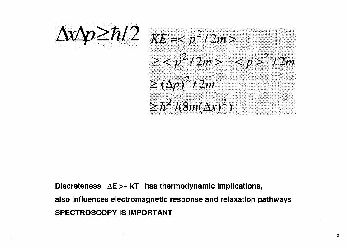
KE=<p2/2m>
><p2/2m>-<p>2 12m
>(Ap)2/2m
Discreteness AE >~ kT has thermodynamic implications,
also influences electromagnetic response and relaxation pathways
SPECTROSCOPY IS IMPORTANT
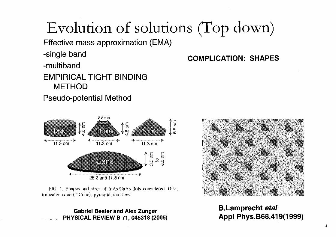
Evolution of solutions (Top down)Effective mass approximation (EMA)
-single band
-multibandEMPIRICAL TIGHT BINDING
METHOD
Pseudo-potential Method
COMPLICATION: SHAPES
11.3 nm
2,3 nm* V.
11.3 nm
/ • . ' • • '
i
11.3 nm
ec
CD
26,2 and 11,3 nm
FIG. L Shapes and sizes of InAs/GaAs dots considered. Disk,iruncateci cone (I,Couc)s pyramid, and lens.
0^
b
[ '
> i~
Gabriel Bester and Alex ZungerPHYSICAL REVIEW B 71, 045318 (2005)
B.Lamprecht efa/Appl Phys.B68,419(1999)
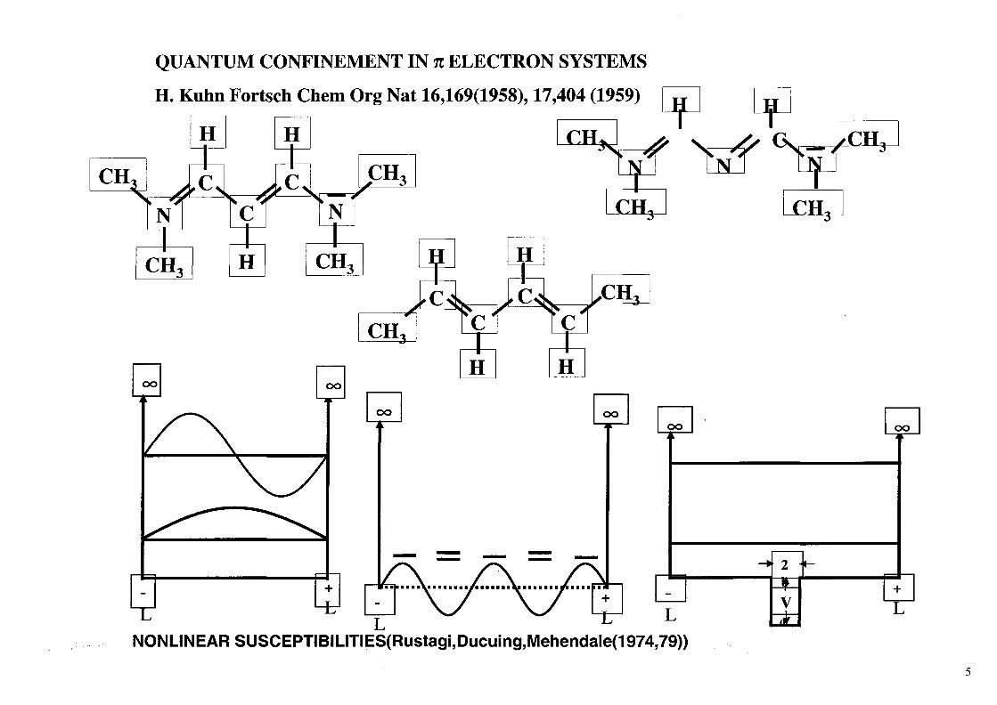
QUANTUM CONFINEMENT IN n ELECTRON SYSTEMS
H. Kuhn Fortsch Chem Org Nat 16,169(1958), 17,404 (1959)
CH
Nz
oo
L
H
H
H
N
CH,
oo
+-t
CH,
CIL
oo
H
cH
oo
CH.J \
1 " 3 '
NONLINEAR SUSCEPTIBILITIES(Rustagi,Ducuing,Mehendale(1974,79))
oo
-
ooi
L
2 •
IfV
i
dr
t-
4
L
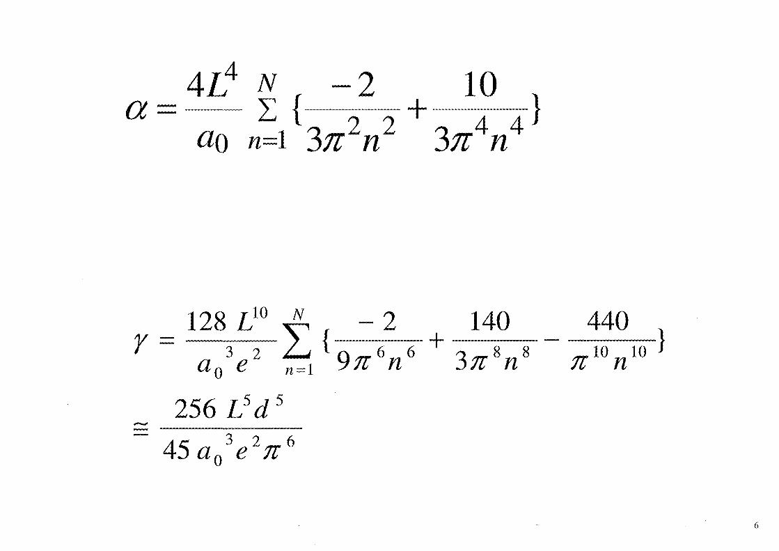
ys J4Ta0
2
V
/«y .|128 L10
3 20 e n
26 . 6 8
256 5 .r 5

10r32
io-3 3
10-3 4
io-3 5
10-36
<Y> en uesTT I Dodecapreno
J P-Carotene
FTGURE VI 1 6
Comparaison
theorie - experienceans
/6-Carotene
Allo-ocimene
HexeneHexan
Doubles liaisons
J_ 2 3 6 11 19
RESONANT ENHANCEMENT
J.-P.Hermann These(1974)
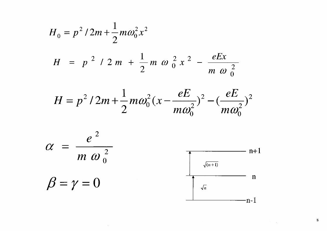
1 2 2
2 °
H = p2 I 2rn + —m a* I x2 eEx
m co o
= p /2m +—mco()(x2 2
020
x
a =m co 0
n+l
n
-n-1

One dimensional metal One dimensional semiconductor
G
Anax ~ + A/If
Localized perturbation in the middlelowers energy of alternate levels
i:B IL
ENVELOPE APPROXIMATION GOOD
G/2

JP =<n H'\n>
....depends on |\|/|2
at impurity position
IN QUANTUM CONFINED SYSTEMSEFFECT OF SUBSTITUTIONDEPENDS ON POSITION OF THEIMPURITY
10

For linear conjugated chains:
Rustagi and Ducuing Opt Comm 10,258(1974)
Nonlinearity increases rapidly with chain length
And with "anharmonicity"
which can be increased by chemical substitution
Mehendale and Rustagi Opt Comm 28,359(1979)
In NONLINEAR OPTICAL PROPERTIES OF POLYMERS(MRS, 1988)S.H. Stevenson et al (DUPONT)
....as predicted by Rustagi, significant enhancement of third-ordernonlinear polarizability in a linear conjugated system can be achieved bysimple structural modifications which act mainly to increase theanharmonicity of its representative effective oscillator,.
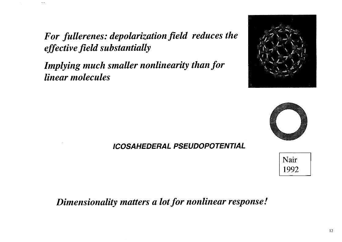
For fullerenes: depolarization field reduces theeffective field substantially
Implying much smaller nonlinearity than forlinear molecules
ICOSAHEDERAL PSEUDOPOTENTIAL
Dimensionality matters a lot for nonlinear response!
12

Interbandtransitions
donor
Acceptor
13

EFFECTIVE MASS OR ENVELOPE FUNCTION METHOD
H = KE + V'periodic +Viimp
= i//{r)uc(r)
(p2 llniif +VimP)y/(r) = £y/{r)imp
effective mass
n2/mi/=d2E/dkidkj
Main Assumption : V- varies slowly over lattice constant
GENERALIZED TO DEGENERATE VALENCE BANDS
Kohn and Luttmger (1955) D . _ „ . . / 4 f t M V ,x u u •*• RJ Elliot (1956) for excitonsfor shallow impurities
14

Quantum confined systems
* imp • * confinement
y confinement = V(z)
con
yconfinement
= y/(r)uc(r)
Quantum Well
finement = V(x, y) Quantum Wire
Quantum Dot/BOX
(p2 I Iniif + Vconfinement )V(?) = eij/{f)
15

Quantum Wells
Assume: confinement potential slowly varying
uc, uvsame in the two materials
SOLVE ENVELOPE FUNCTION EQUATIONS
MATCH AT THE BOUNDARY z= +L,-L
PROBLEMS:
1. Barrier height? Quite often inferred indirectlyfrom optical spectroscopy using rather simpletheories, so still changing
Wlbarrier +
pz/2m ->pz(llm (z))pz
e.g., M.AItarelli in lnterfaces,Quantum wells,and superlattices,
eds Leavens and Taylor,Plenum (1988)
Refs: G.Bastard" Wave mechanics applied to semiconductor heterostructures,Les Edision de Phys(1988)
C.Weisbuch and B.Vinter Quantum Semiconductor structures,Academic (1991)
16

Spherical Quantum Dot/-I 1 / 2 1
ni
\R
\
J
n2m R
zeros of the spherical Bessel function
Cylindrical Quantum Dot
— t s in i F=L2.
O fP
n = 1 - - - 9
17

MULTI BAND EFFECTIVE MASS CALCULATION
W-372
u3/2=
X-iY>l/j2\X+iY>T/42
8
MI/2 =| X-iY>1~/46 +V273| Z
E(k) = (fi212m)(nk2
2 , 4 2 ,,,2\/r_2r_2 . 7,2 r 2
J.M.Luttinger Phys Rev 102,1030(1956)18

P3/2 ~S R 0
Pl/2 0 R
v
R
0
0 P-i/2 S
R S' P-3/2
Pill = P-3/2 = Vik2 + y2(k2+k*-2k2)
Pi/2 = £-1/2 =Vik2- V2 ikl +k2y- 2k2)
R = -(V3 / 2)(y2 + 73 )(kx -i
= 2/Sy3kz(kx-iky)
\
J
3 - y2 )(kx + iky
Yl Luttinger parameters
k /V To get envelope equation
J.M.Luttinger Phys Rev 102,1030(1956)19
For semiconductor quantum dots grown by soft chemical methodsconfinement potential is relatively large and can be assumed to beinfinite.In semiconductors confined by a larger gap semiconductor the bandoffset is generally small ~ 0.1 to 1eV Resulting finite well problem isgenerally more difficult to solve
Also boundary conditions uncertain, but perturbative treatment possible forsmall variations in shape.
20

Empirical Tight Binding methodP.E. Lippens and M. Lannoo, sps*Phys. Rev. B 39,10 935 (1989)
S. Sapra, N. Shanthi, and D.D. Sarma,Phys. Rev. B 66, 205202 (2002)S. Sapra, and D.D. Sarma,Phys. Rev. B 69,125304 (2004)
for II-VI COMPOUND QUANTUM DOTS sp3d5
"Direct diagonalization methods are practical only for clustersizes containing less than ;1500 atoms. For larger clusters, weuse the Lanczos iterative method"
ZnS ZnSe ZnTe CdS CdSe CdTea(A) 5.41 5.67 6.10 5.82 6.05 6.48Ns N d(A)12 1285 36.49 38.24 41.14 39.25 40.80 43.70
EFFECTIVE BOND ORBITAL MODEL(Y.C. CHANG)
REDUCED NUMBER OF ORBITALS CAN MANAGE LARGER PARTICLES
ALSO FEWER PARAMETERS, BUT NOT FROM BASIC THEORIES21

VALENCE BAND MODEL 6orbitals = x T, x I, y T, y I, z T, z I,Y.-C. Chang PRB 37,8215(1988)
< Ra IH I R'ct >=
I SR-R'AExyTaTa' ( 1 " Sact) + [ExxTa + Ezz (1
|R,a> orbital at /? and a= x,y,z x nearest neighbor displacement vectorsE site energy, Exx,Exy,Ezz interaction energies
Conduction Valence Band Model
r
Nair,Ramaniah,Rustagi PRB 45,5969(1992)
22
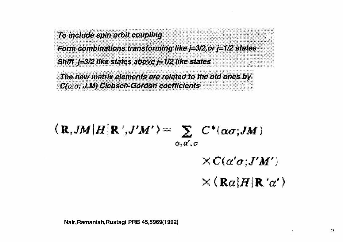
To include spin orbit coupling
Form combinations transforming like j=3/2,or j=1/2 states
Shift j=3/2 like states above j=1/2 like states
The new matrix elements are related to the old ones byC(a,o; J,M) Clebsch-Gordon coefficients
C*(aa;JM)
Xda'oiJ'M'
Nair,Ramaniah,Rustagi PRB 45,5969(1992)23

USE SYMMETRY TO REDUCE MATRIX SIZE
FORM LINEAR COMBINATIONS THAT TRANSFORM LIKEIRREDUCIBLE REPRESENTATIONS OF TETRAHEDRAL GROUP
Uy
n th component of F, irreducible representation
24

FITTING PARAMETERS NEAR ZONE CENTER
Me *flf /21S
TABLE II. Tight-binding parameters for VBM and CVBM* which reproduce band strecture close tothe F point accurately* ^'0—^/2moa2
: _ _ ______
VBM CVBM
f'Eg
+ A J J
jc s-jg" — fgjG* -4-4F
Nair,Ramaniah,Rustagi PRB 45,5969(1992)
25
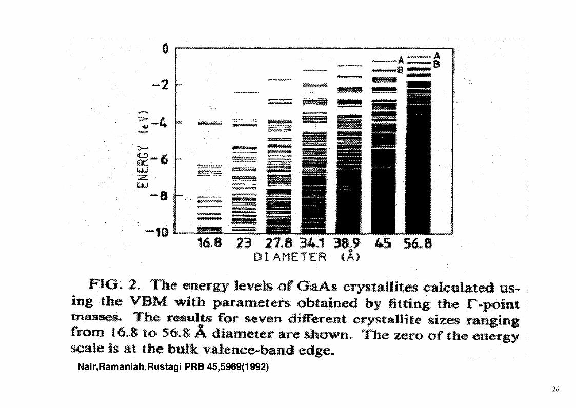
.8 23 2X8 34J 38.9 45DIAMETER t i l
FIG. 2, The energy levels «*Ing. the VBM with parametersmasses- The results far seven, diirenent crfroro 16,8 to 56,8 A diameter mm shown.scale is al the bulk eb
Nair,Ramaniah,Rustagi PRB 45,5969(1992)
of the mmmn
26

- 2 -
16 J 23 .27,8 34 J 38-9 45 56-8
CVBM. The positions of the bulkedges are indicated by dotted lines
Nair,Ramaniah,Rustagi PRB 45,5969(1992)27

35UJf
2.5
s
• * « ^
i
DIAMETER
IG. % The sizecrystallites. Theciil&tion usingmass cakwlatiiand a single-band model forcleg represent experimental
of- the aiGiton position in CdSthe reswJi of a tight-binding cal-
da&hftd line is given by an effective-model for the valence
a (Ret 7).
Nair,Ramaniah,Rustagi PRB 45,5969(1992)28

TABLE 1. The onfmerneiil energies <in -cV) for a few cop*mm% valefNte-tnMid levels in- CtfS quantum dtols, The symmetry
Diameter U»e-te«l MulEMA
70 a03tt G.07fr<Fif> 0,07
J» 0.130 0L234i (rfr+J a 19
J47 err) -mis
12ft O.S?6(r/) 0.43QLfiO6> 0 V )0.743 er r *0.791 ( r r > 0^46
Refs: Colvin et al PRL 66,2786(1991), Nair et al PRL 68,893(1992)29

DIAMETER (A3
FIG. 5, The siie dependence of a few topmost valence-bandlevels (circles, crosses, and dote) in GiAs crystallites obtainedusing VBM, The solid lines represent the corresponding resultsgiven by a multiband effec-tive mass calculation, The notationn T~ stands for the nth level of TJ
Nair,Ramaniah,Rustagi PRB 45,5969(1992)
30

§ 0,2 0,4 0,6 0.8 1 0 0-2 0.4 0.6 0-8 I
FIG, 6, The lowest two / = 0 EM A envelope functions for theconduction band obtained ysiug a single parabolic tend modelwith a confining potential of 10 eV jsolid line) compared wilkthe corresponding wav£ function given by CVBM for GaAscrystallites (open circles). The results for two crystallite si»esare shown,
Nair,Ramaniah,Rustagi PRB 45,5969(1992)
31
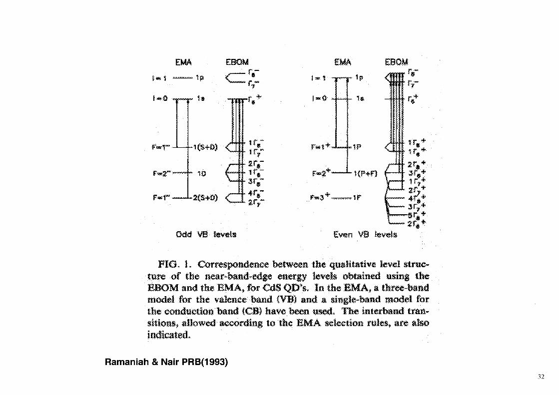
t • 1
1*0
EBOM
-1CS+D)
IP
irT
1 0-
EBOM
Odd ¥i ;
-IF
Even VB fevets
turn of the itear-banjdrEBOM md the EMA,formodel for the valencthe conduction band {CB
bttwetn the qualitative level atrne-energy leveb obtained using the-:
Q P U .In.:-the EMAt a three-bandCVTO and a single-band modBl for
been used. Hie interbaiid tran-the EMA ateciion rutei, are also
Indicated.
Ramaniah & Nair PRB(1993)32

WAVE VICTOR
FIG. 1. The calculated band stmcture of tinconduction bands for GaAs along the T-X direction using aneffective bond-orbitai model with parameters obtained by Itttagthe bulk F-point masses. The dashed lines are obtained in avalence-band rawd«l (VBM), while the soUd'fines are given bythe CVBM which inclwdes a condnctlon^band orbital a!s»; both•give identical dispersions for the heavy-hole band. The parabol-ic dispersions given by the band-edge masses are also shown(dotted lines).
Nair,Ramaniah,Rustagi PRB 45,5969(1992)
33
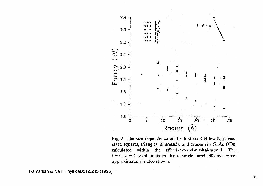
>CD
2.4 -
2.3 -
2.2 -
C 1-9
r*# r
* • *
*I I
I
1,7
0 • $ 10 IS 2.0
Radius (A)Fig. 2. The size dependence of lite first six Cstars, squats, triangles* diamonds, and crossescalculated within the effective-bondI = 0 , it ss 1 level predicted by a singleapproximation is also shown.
levels, (pluses.in GaAs QDs,1-modeL The
ive mas
Ramaniah & Nair, PhysicaB212,245 (1995)34

tu
Fig, L TIthe
Ramaniah & Nair, PhysicaB212,245 (1995)
35

SELECTION RULESband index,
= YJ\dkAb(k)efk:rubl(r)
\eik-rAn(k)dk
Fnlmv
36
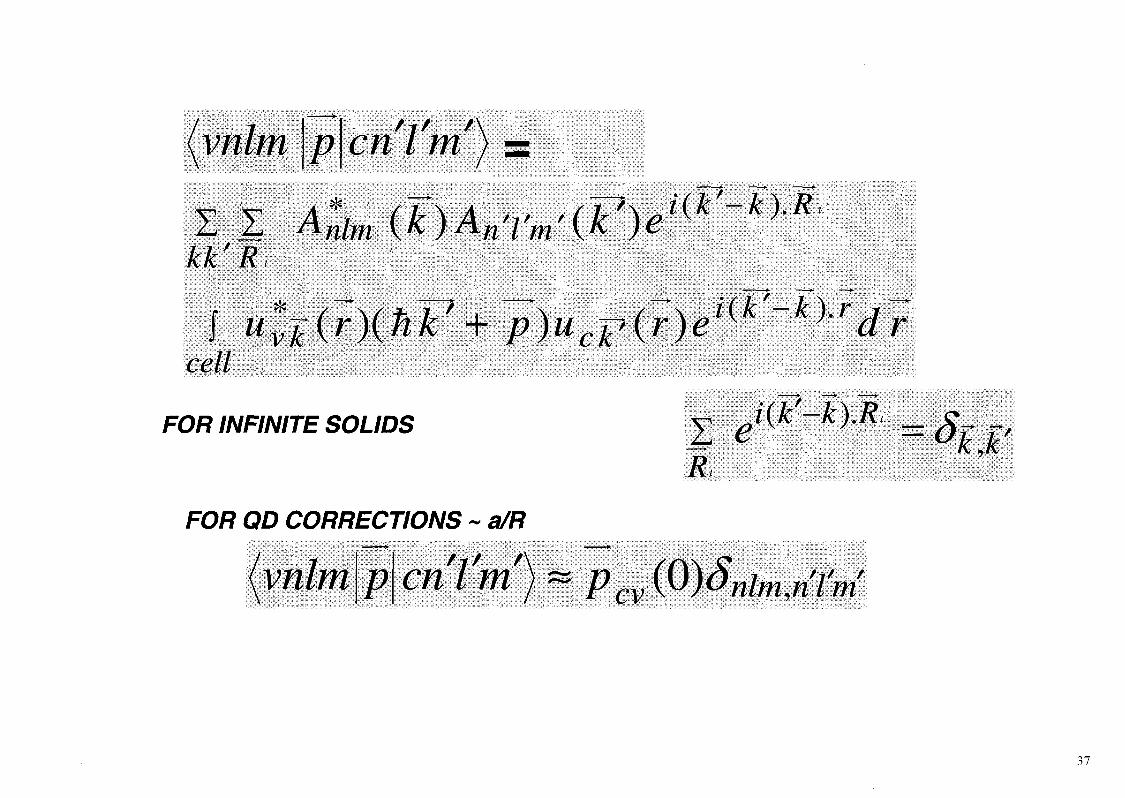
vnlm
Z Zkk'R,
p*
i lm ) —
(k)An'i'm'(k')e i(k'-k).R,
p)ucell
FOR INFINITE SOLIDS
ck'
Z e' _ ?
FOR QD CORRECTIONS ~ a/R
vnlm p cril'm) « pc v
37

IF Pcv(0) =
(vnlm\p en I'm
M jUV
cv dkk=0
\
Transition Rate - 1/R2
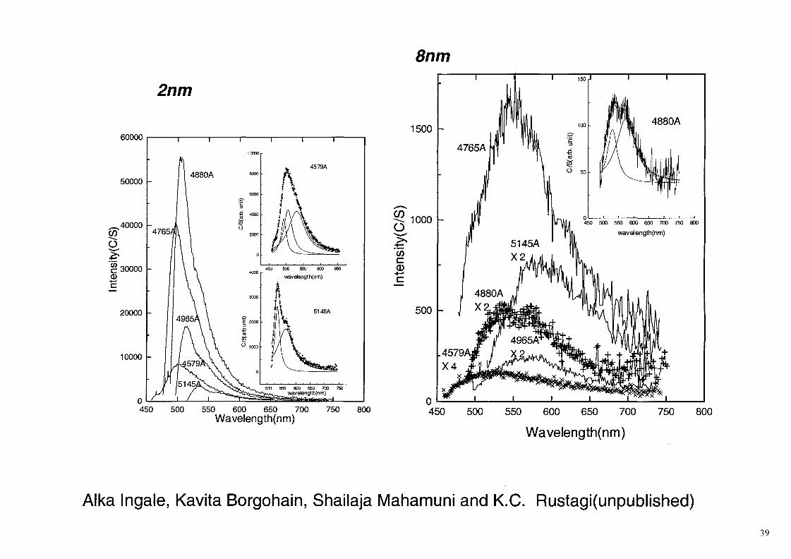
Alka Ingale, Kavita Borgohain, Shailaja Mahamuni and K.C. Rustagi(unpublished)38
8nm
C/)
O
'55CD
2nm
60000
50000 -
40000 -
30000 -
20000 -
10000 -
450 500
1
• /
f 51/ i
i
4880A
1
\ \
\ \ \
/ i
1
arb.
uni
S£o
C/S
(ait)
uni
t)
10000
8000
6000
4000
2000
0
4000
3000
2000
1000
0
1
¥450
A
t
500
i i
% 4579A
'A500 550 600 650
wavelength(nm)
I 5145A
550 600 650 700 750wavelengthfnm)
550 600 650 700 750
Wavelength(nm)800
1500 -
CO
oCO
CD
1000 -
500 -
450 500 550 600 650 700 750 800
wavelength(nm)
450 500 550 600 650 700
Wavelength(nm)
750 800
Alka Ingale, Kavita Borgohain, Shailaja Mahamuni and K.C. Rustagi(unpublished)
39

structural changes also change energy levels!
Ai RI-V:I-:\V H 71. I M M I
< vlnnhicaMy shaped /inc-hlcudc semiconductor quantum dots do not have cylindricalsymmetry: Atomistic symmetry, atomic relaxation, and piezooloctric effects
ne] 1J»JS:CT ;uid Alex Zi.Mp.erNational litiwwiihtc r.mi^y Uihumtory, (iotth-n. ('oforutfo •Sfiihl, USA
n<i-«-civ«il 1 April .'(KM: published 11 .'anuaiy .'OO.M
Se.lt ii.w*mhled quaimim dots ate ol^en modeled l»y continuum models (elfective mass 01 k p ) Ili i i! issmnetin1 syniiiietiy of the dot tc hi.' that oi its owral l /•comc'.iic slripi:. Lens shaped or conical dots aie thus assumedto have cvwilitiuous eylhuin(\il s=\jnjiK.'tty ('.,.. W!K*U.'H> :>yi"imi(l.il ilM* me !i-;siu:n\i tn have (',-.. syimiKitiy.However, considering, t:i;it the III V tints are m:ide ol" .'ilmn^ mnuif-ed on llie (it:hixi:d) positions ci' ;i .'iil:le:ivii.' lattice, one would expect tl.e lushest [>ossihle syiu;netiy in these stnictuurs to he Cj... hi tiiis syin1'ioup :ill Maies :'.ie .siri<',ly di^e-.iei.'.te and thuie nc no n priori iwistm to expect. e.,f.. the I'lechon / ' >\u(nssually the .second ;i:id third eii-cHi)n !evd> of (JomiiKmi oihit.il P cl:aiacter) to he cli^-eiieiiitc. ('<mtii:uuuinioik'ls. hovu-viM. p:edict thes-.1 states To he. eiierp.eiically (U*;\;MKMi:te unle>s tin hre^uhir .shape is postulated. WeS'IOW that, in fact, the tine (aloir.i.Mie) .synmietiv oT the dots is ivviirtled when tin- elVecls i'.t'(i) inleil:ici;ilsynuiiL-tiy, (ii) .ltoiniMic si rain, i.nd (iii) piivoelectiicity me taken into HIVOIIMI. W:.* (junntity the contnhution>(M" each of" thestr etlbcts separ.'itoly liy culciihitin^', tin: splitting of election I* levels 1oi dit'leienl dot shapes atdilleiciit levels of Iheniy. We rind 111-it lor mi ideal Mniate-h.'iscd pyr.iuin<;il luAs-'Cia^s dot \\\v. inttM facialsynsnietiy oTtln.- uureiaxed do: splits the P level by J.{J meV, atomistic lelaxatmu iidds a splitliuf-, of IK.* nieV(zero ilcoiitiiniiMii elasticity is used to cdcukit*.1 strain) and piezoelectricity i educes the >pl:tlinf- by X.4 meV.lor n total splitting of 1 .;.S meV. We iii i lhcr ;:liow ihut tin: :itonustic efleets \\) and (ii) favor an oiientation el"ihe ek'ctror. m n v functions ;iloii>\ the [ I lf!| diieclion while el led {ii i) favoir- tlie | J10| directiiMi. Wlieiea1-eilects (i) r (ii) prev.nl for ,i pyi;n.u!al i loi, foi :i lens y.iaped dot. eliect (iii) is dominant. We sh.»v.- thul tlsefc hand U p • net hod. applied to puamii lal inAsXi.iAs dots ilesenk's iiiconectly '.he :-.phltm{' and o:de;- of1* levels { li i:ieV insicau of I I meV piitlnif',) and yields ;!n- oi iei:i.i:ion |"I1O| iuMead o f ; 1 IO|.
40

ENVELOPE FUNCTIONS FOR OTHER SHAPES
41
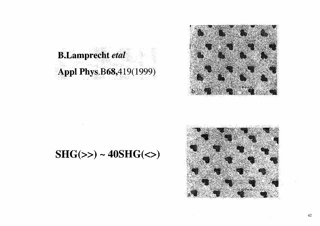
B.Lamprecht etal
Appl Phys.B68,419(1999)
SHG(») ~ 40SHG(<>)
V.-,
#
42

METAL NANOPARTICLES
Third harmonic generation in metals was measured by Burns andBloembergen in 1969
Theory? Free particle nonlinearity negligible
Surface? Collisions? Higher order multipoles?
In nanoparticles: %V\ff= % ( 3 )m e t a l / 2 | / | 2
, = 99?metal
Size quantization main cause of nonlinearity
43

0
Po
Fiasy solutions for apexanglc=7i/inlcger(X)
X=l means hemisphere
44

Cylindep X = 1 X = 4
cLU
0.1
0.09
0.08
0.07
0.06
;0.05
0.04
0.03
0.02
0.01
01
values
1 8
45

Sphere Sector (X=1) Sector (X = 4) lvalues
0.5
"«*»«»»——™~~«»^™~»««
o1
1 2 3 4 5 6 7 8
46

Spherical Quantum Dot
2 1 / 2
RJi
\
R\ J
Eto 2m R2 5 N / b nl zeros of the spherical Bessel function.
Hemispherical Quantum Dot:
Out of these solutions,select those which vanish at z=0 plane
Lowest state 1=1
For same volume :
I hemispherical QI) has larger confinement energy
47
Effect of electron-electron interaction Dielectric Confinement
Screening - depolarization field,sensitive to shapeplasmon resonance -Correlated motion :beyond single particle picture
Generalized Kohn Theorem
Interacting electrons in Harmonic oscillator potential absorb only at coo
Screened y = single particle y . local field factor
) =1
_abc
~3 J
L x ( edq
xx
2 , 2\l/2
For long molecules: L
48
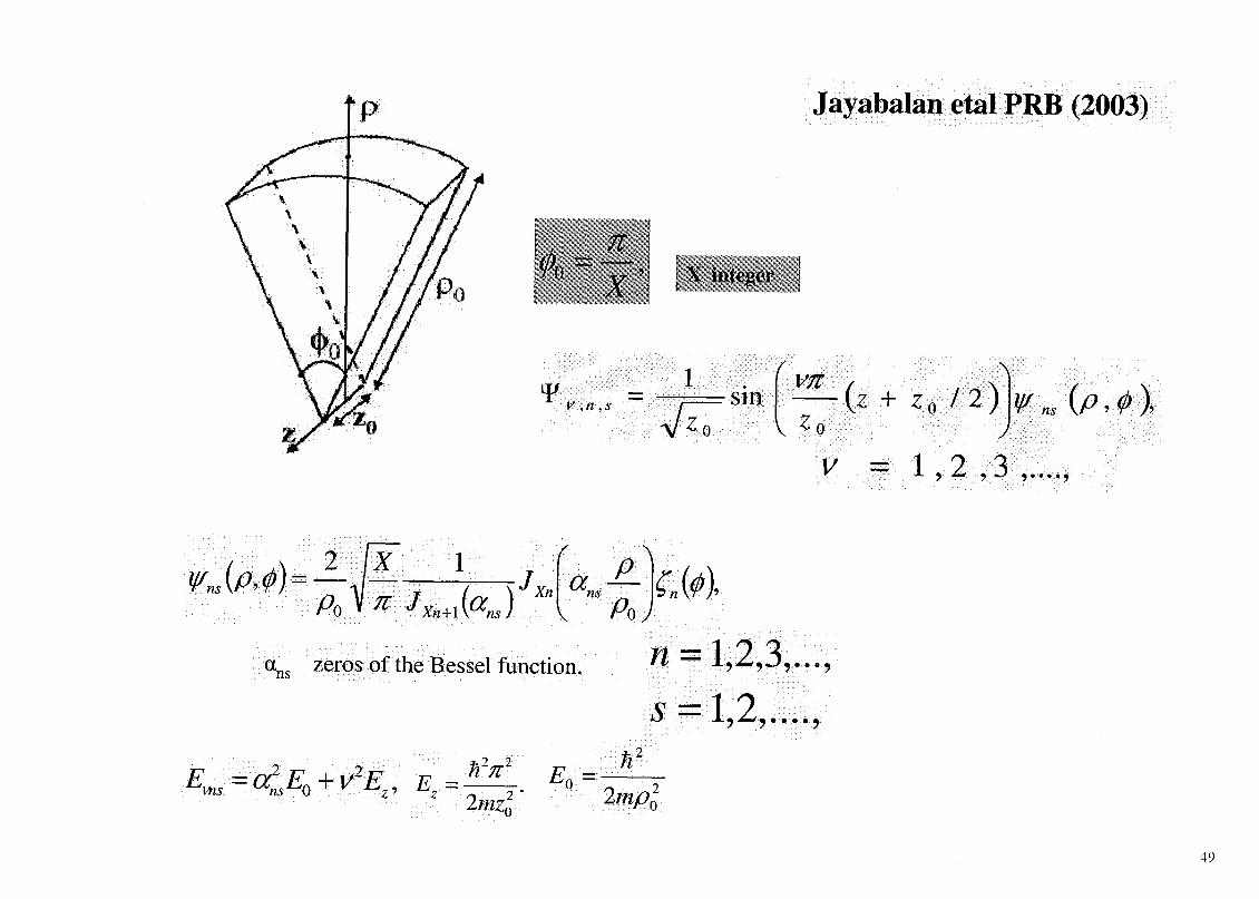
Po
Jayabalan etal PRB (2003)
n :'0 "" TT-' | X integer \
v ,n ,s sin + Zo 1 2 )0
v = 1 2
2Xn a. P
ns\
ans zeros of the Bessel function. IV
49

Electronic density Jayabalan etal PRB (2003)
o
50

1000-
CD
oI—
X
2CD
DC 100-
0.011/X
Jayabalan etal PRB (2003)51

100 -
oX
caCD
DC
1 0 -
1 -
0.01
1/X
Jayabalan etal PR B (2003)52

\
(a) (b) (c)
Jayabalan etal PR B(2003)
53

EXCITONS
Exciton wave function has the form:
= y/(rhr2)uc(r\)uv(r2)Envelope function varies slowly and obeys wave equation:
2m 1 2m 2
With boundary condition:
—0 for
Nair,Sinha,Rustagi PRB (1987) 54

LIMITING CASES(Efros & Efros(1982))
Strong confinement Confinement energy<coulomb energy
Weak confinement: Confinement energy<coulomb energy
Exciton with quantized center of mass motion
J7 77E = E8 ex 2MR2
* t* in
Not compatible with boundary conditions
55
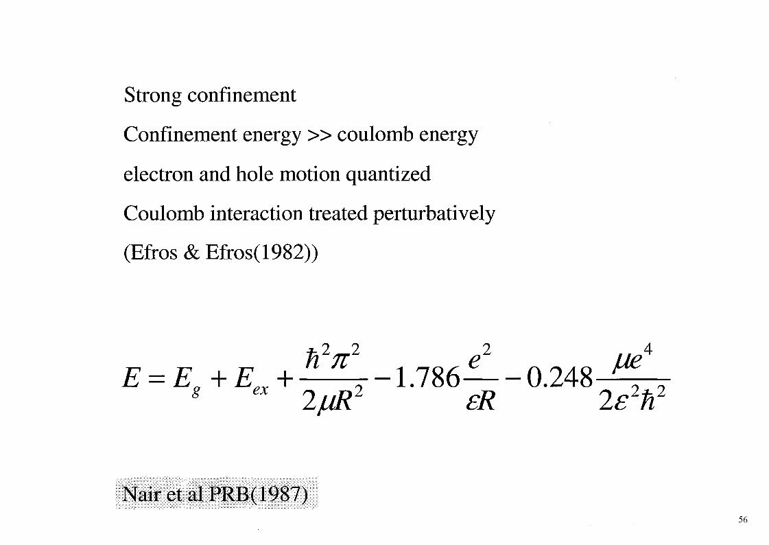
Strong confinement
Confinement energy » coulomb energy
electron and hole motion quantized
Coulomb interaction treated perturbatively
(Efros&Efros(1982))
2 4
-1.786-—0.2488 " e x 2juR2 sR 2s2fi2
NairetalPRB(1987)56

NairetalPRB(1987)
Variational calculation with trial wave function:
/R
a, i sin( vri /R)
r2/Rfor
0 outside*
Centre of mass quantization?
= E*+EeX8 2M(R + d)
See Also Kayanuma SSC (1986),PRB (1988)57
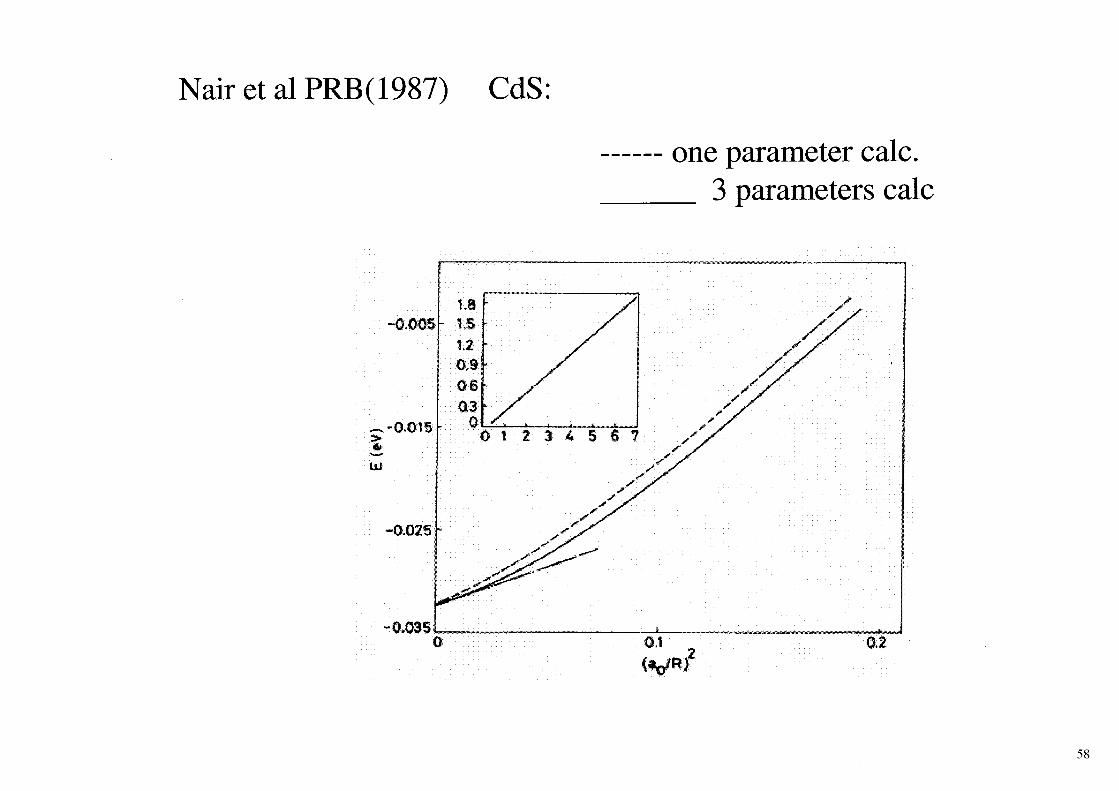
NairetalPRB(1987) CdS:
one parameter calc.3 parameters calc
-0,005 -
-0015>4b
UJ
-0.025 *
0.03S
58

Nair et al PRB( 1987) CuCl
0.5
59

Biexcitons in Quantum dots and nonlinear response
Nair and Takagahara PRB 55,5153(1997)
_ _
Xexp,-rd l
II•71
Zffli'T2
"1 •I J
%S'AMs-&<
£'
2'
i / j
60

Nair and Takagahara PRB 55,5153(1997)
fa) without exchange
Radius (R/a-_)
FIG. 2. Calculated energies of the hicsciton states ia) without and fb-di with the electron-hole exchange interaction included.JU', A'VO (XVO',), XXI t and XX2^ respectively, denotse the biexciton ground state and the weakly correlated exciton-pair states withJ~ 0. lj and 2. Notettions are the same as in Fig. I.
61

i 12
T retina IL ~ 194_4?rie V4.
80 100
FJG. 3. The calculated size dependence of the biexciton bindingenergy in CuCl quantum dots. Two sets of results corresponding tothe exdton Rydberg. E% —194.4 meV and 213 mcV are shown. Tlieexperimental results of Ref. 40 are also shown.
62
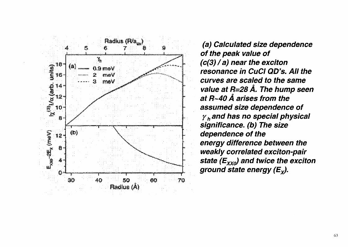
.9 m©V2 meV
40 50 t €0Radius (A)
Calculated size dependenceof the peak value of(c(3)/a) near the excitonresonance in CuCI QD's. All thecurves are scaled to the samevalue at R=28 A. The hump seenat R~40 A arises from theassumed size dependence ofyh and has no special physical
significance, (b) The sizedependence of theenergy difference between theweakly correlated exciton-pairstate (Exxo) and twice the excitonground state energy (Ex).
63

Experimental details from K Matsuda et al PRL 91 (2004)
(a)
Q
6
CL
i.eoPhoton
Probe
64
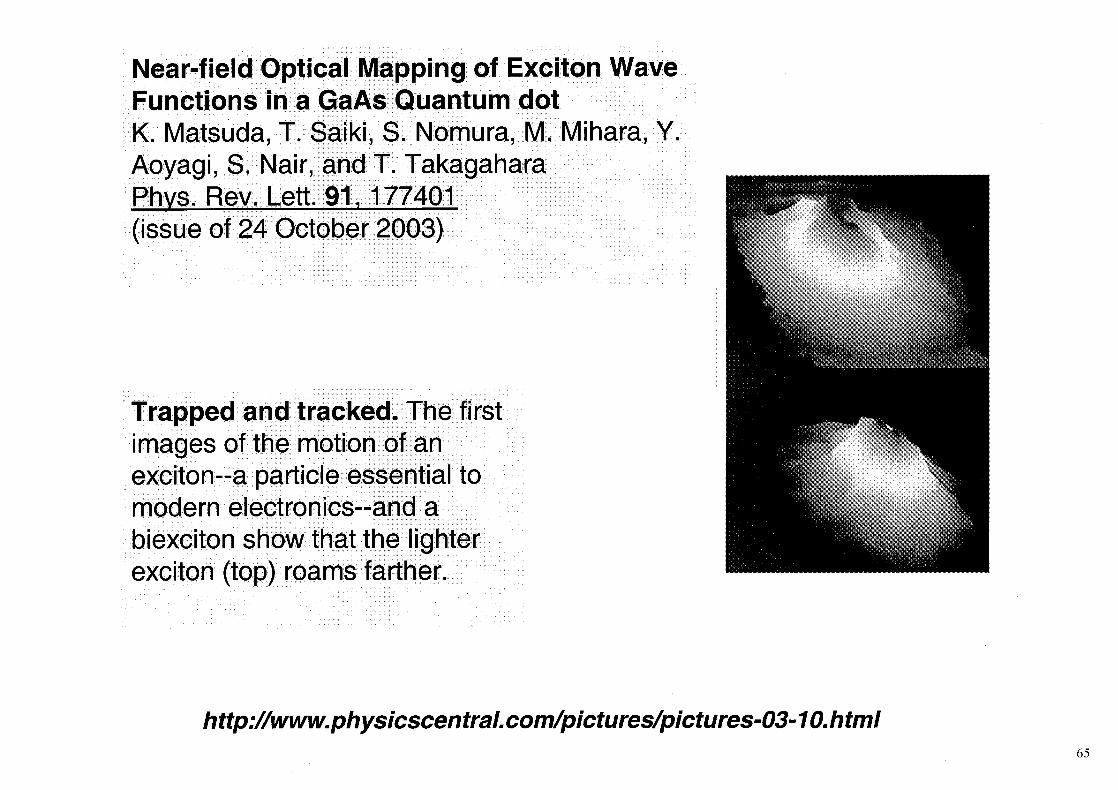
Near-field Optical Mapping of Exciton WaveFunctions in a GaAs Quantum dotK. Matsuda, T. Saiki, S. Nomura, M. Mihara, Y.Aoyagi, S. Nair, and T. TakagaharaPhvs. Rev. Lett. 91, 177401(issue of 24 October 2003)
Trapped and tracked. The firstimages of the motion of anexciton-a particle essential tomodern electronics--and abiexciton show that the lighterexciton (top) roams farther.
http://www.physicscentral.com/pictures/pictures-03-10.html65
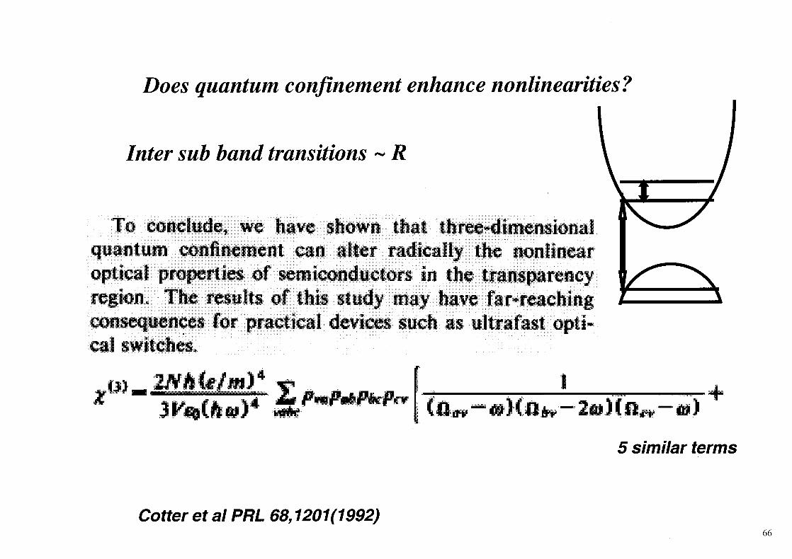
Does quantum confinement enhance nonlinearities ?
Inter sub band transitions ~ R
To conclude-, we have shown that three-dimensionalquantum confinement can liter radically the nonlinearoptical properties of semiconductors in the transparencyregion. The results of this study may have faroeachiiigconsequences for practical devices such as ultra fast opti-cal switches
—m)
5 similar terms
Cotter et al PRL 68,1201(1992)66

0.5FIG. I. The solid curves show a typical model calculation of
X{" for a sphere of radius a—5 nm with m,-—0.15m, m,.'-0.8/w, tuo -1 .17 eV < 1.06 /im), At ' -35 meV, j /M-0 .2 , and>; — 0.01. The dashed curves are for the same semiconductor pa-rameters and number density, but different radii a. The curvesare plotted vs the normalized photon energy Aoi/fio, taking Ko
as a variable parameter. The distinctive features of these curvesarc found to be typical of quantum-confined particles (and arerobust to changes in parameters), but quite different from thoseof bulk semiconductors [21. Values of Im* 0 ' (solid circles) andRe*0 1 (open circles) measured at l.06-/mi wavelength for 24semiconductor-doped glass samples are shown.
Cotter et al PRL 68,1201(1992)
67

RQ716
9f* BWSffP^&&vy/i ~f8jQ|
Pig, 2L Reflectivity versus intensity for some SDG'e, Data, aimtaken with/f bt and p in temporal coincidence and with parallelpoLarLEations. Sample thicknesi;, 3 mm Solid linea? JJ5 *K IQ ]dotted lines, R m 1^, The intenEity at the interference maximaof f and 6 is =" S-GI 'M 1$,
Banfi et al JOSA B 12,621(1995)68
Cotter et al( 1992): Semiconductor doped glasses havelarge third order non-linearity of electronic origin(75pspulses)
Quantum confinement enhances nonlinearity!
Pavia group: fifth order nonlinearity at relatively lowintensities (35 ps pulses)
Bindra
Repeated DFWM and z-scan with 20ps pulses
Nonlinearity apparently fifth order at low intensitythird order at higher intensities!
So THE PROBLEM IS REAL!
69

Resolution:
Nonlinearity is indeed fifth order, but at higherintensities there is saturation of DFWM signal due tononlinear absorption
Probe beam intensity is much reduced because of TwoPhoton absorption and linear absorption by thegenerated e,h's
Similarly , z -scan signal at higher intensities saturates
Bindra et al PRB (1999)5Opt Comm (2000)70

FIG. 7. Sample length is ditridjod into equal segments oF thiiak-Az. Tba fimmui. and backward pump beams? ibr ,r - 0 M Ucne
.. _ j r au inoixkiil: an Jkos z and zw of thi saiTipb?
S/nc/ra ef al PRB (1999)
mm)
FIG. 3, Energy tatnanuaiism ftr fetwrard pump beam (a) wtenonly forward pomp beam is present, fb) in the presence of all inter-acting beams. The solid line shows the rodnction ctfpeak intensityof Forwsrd pump beam M, the piesenGC of all hcEims.
71
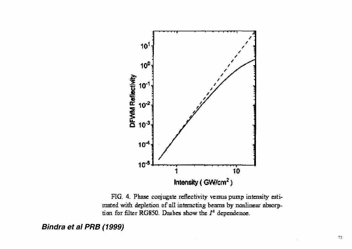
FIG. 4. Pluas conjugate ;rdleeti¥ity VEIBUS pump inmated witii depktkm of ell interaetiiig beami bynmi For £Q,ter RGI50. Dailra siiow ihe /* dcp^idcnoe.
Bindra et al PRB (1999)72

Intensity dependenceAn/I and T
p-v
200 i-
a
X 2
2.0
1.5
10
O.i
0.0
Bindm et al Opt Comm (2000)
•
i r1.2
^ : • • • • * ' •
I
p-0.2cm/QW
1 , 1 . 1 . 1
4 i-
6.6S
10
I
15
m
1.2
an•i
1.2<M OS
UJU*0 2 4 i :: S
0 ^
0.0
1.2
0.0
0,4
S
, i
0 10 20 30
II73

100 fs
m
OJ
-20
6ps
ion
rran
smi
ized
Nor
mal
1 «
0 . 6 -
0 . 2 -
O Oo o 1
\ /1/49
-10 -S 0Z(cm)
10
FIG. 1. Closed-aperture z-scan for the sample RG850 with 6 ps pulses.
V
\vit!» » - ( b ) .
TPA generated e-h pairs
Generated carrier absorption
0 10
FIG. 3. dosed-aperture z man for the sample RQ850.. Circls are te ex-perimental data points. Solid line is the fit obtained with TPA coefficient=6xlG~La> raw1, free carrier cros; seclion=—LSXlO"22 cm1 and «2
= 14x 10"20 m 2 ! " 1 . Curve (b) is obtained by neglecting the effect of n2 <Curve 4c) is; obtained by neglecting the effect of fifth-order nonliniearity.
Bindra and Kar APL79,3761(2001)74
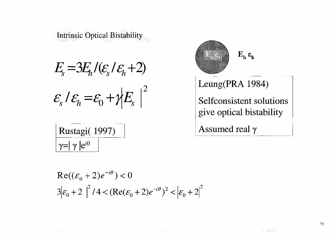
Intrinsic Optical Bistability
Rustagi( 1997)
Leung(PRA 1984)
Selfconsistent solutionsgive optical bistability
Assumed real y
75

ad + (l - a)d
zz
F = F
2k = Er
2m
2m
*
M£
Warburton etal PRL(1998)
0.05
76
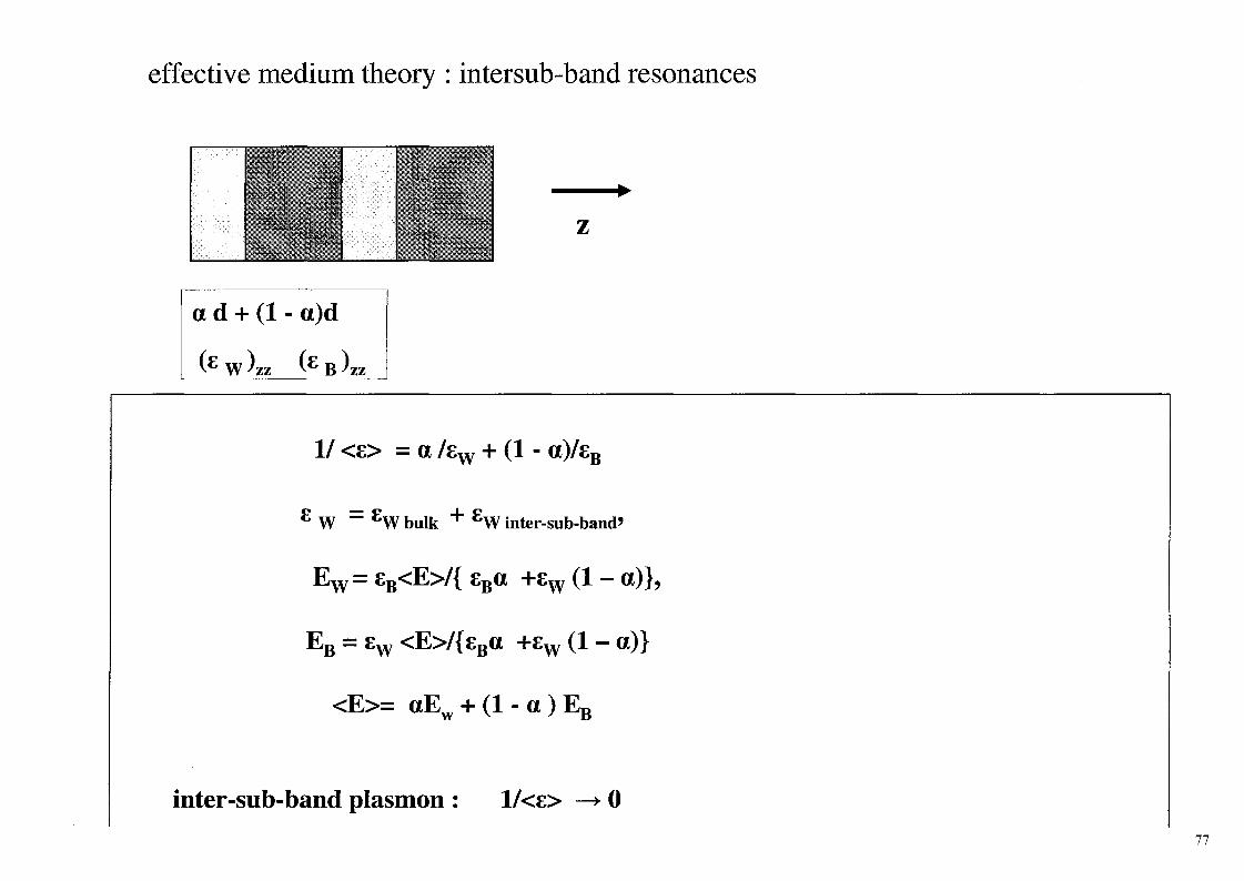
effective medium theory : intersub-band resonances
a d + (1 - a)d
1/ <£> = a /£w + (1 - a)/£ji
£ W = £ W bulk + £ W inter-sub-band?
E w = £B<E>/{ £Ba +£ w (1
EB = £ w <E>/{£Ba +£ w (1
<E>= aEw + (1 - a ) EB
inter-sub-band plasmon : !/<£> —
- « ) }
77

s—.
X
100 110 120 130 140 150 160 170577 K376 K293 K214- K125 K1.0 K
80 9O 100 110 120 13O 140 150 160 170
S Mukhopadhyay+KCR(1999)78

C/}
0 100 200 300 400
Scaled Incident Intensity (y)
500 600
S Mukhopadhyay+KCR(1999)79

SUMMARY
EMPIRICAL PSEUDOPOTENTIAL AND TIGHT BINDING CALCULATIONSBECOMING RELIABLE FOR SPHERICAL QUANTUM DOT SPECTRA
SELECTION RULES LESS STRICT FOR SMALL QUANTUM DOTS
NEAR FIELD METHODS EXCITING FOR SINGLE QD SPECTROSCOPY
SHAPE DEPENDENCE OF QUANTUM CONFINEMENT ANDDEPOLARIZATION FIELDS IMPORTANT
80
ACKNOWLEDGEMENTS:
Selvakumar Nair,
Lavanya Ramaniah
K S Bindra
Alka Ingale
J. Jayabalan
References:
H. Kuhn Fortsch Chem Org Nat 16,169(1958), 17,404 (1959)
Semiconductor Quantum Dots - Physics,Spectroscopy and Applications
Y.Masumoto and T.Takagahara (eds) Springer (2002)
81

One importantadvantage of the TB theory is thit It can treat even non-sphericsl shapes quite easily, whereas it would be practi-cally impossible to solve the corresponding envelope-function equations.
Nair,Ramaniah,Rustagi PRB 45,5969(1992)
82
Related Documents
![Transition from spin-orbit to hyperfine interaction ... · traditional, direct excitons (DXs) in semiconductor quantum wells [25]. Because hole spin relaxation is usually much faster](https://static.cupdf.com/doc/110x72/5e1f39f844e5b7747314401b/transition-from-spin-orbit-to-hyperine-interaction-traditional-direct-excitons.jpg)