Electronics 1 Lecture 4 Bipolar Junction Transistors. Structure, Characteristics, Basic Circuit Configurations, Biasing Literature 1. Tony R. Kuphaldt: Lessons In Electric Circuits, Volume II – AC, 2007 2. Tony R. Kuphaldt: Lessons In Electric Circuits, Volume III – Semiconductors, 2009 3. Tietze U, Schenk Ch: Electronic Circuits – Handbook for Design and Applications, Springer, 2008, ISBN: 3540004297 4. Horowitz, Hill W: The Art of Electronics, Cambridge University Press, 1989, ISBN: 0521370957

Welcome message from author
This document is posted to help you gain knowledge. Please leave a comment to let me know what you think about it! Share it to your friends and learn new things together.
Transcript
Electronics 1
Lecture 4
Bipolar Junction Transistors. Structure, Characteristics, Basic Circuit Configurations, Biasing
Literature1. Tony R. Kuphaldt: Lessons In Electric Circuits, Volume II – AC, 20072. Tony R. Kuphaldt: Lessons In Electric Circuits, Volume III – Semiconductors, 20093. Tietze U, Schenk Ch: Electronic Circuits – Handbook for Design and Applications,
Springer, 2008, ISBN: 35400042974. Horowitz, Hill W: The Art of Electronics, Cambridge University Press, 1989,
ISBN: 0521370957
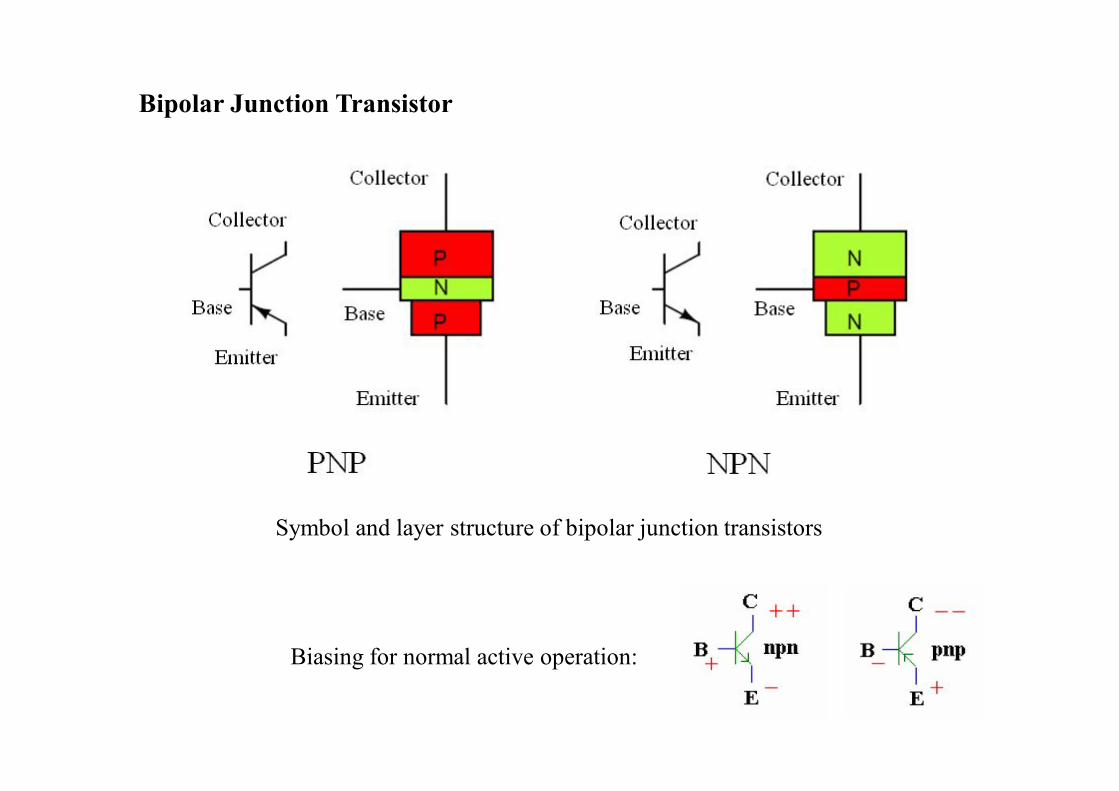
Bipolar Junction Transistor
Symbol and layer structure of bipolar junction transistors
Biasing for normal active operation:
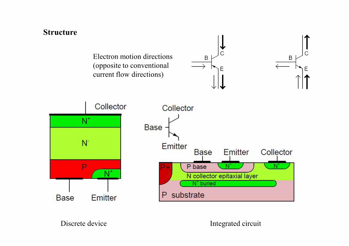
Structure
Discrete device Integrated circuit
Electron motion directions (opposite to conventional current flow directions)
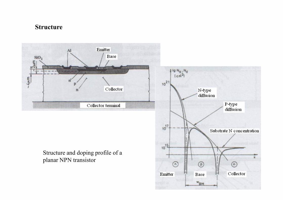
Structure
Structure and doping profile of a planar NPN transistor
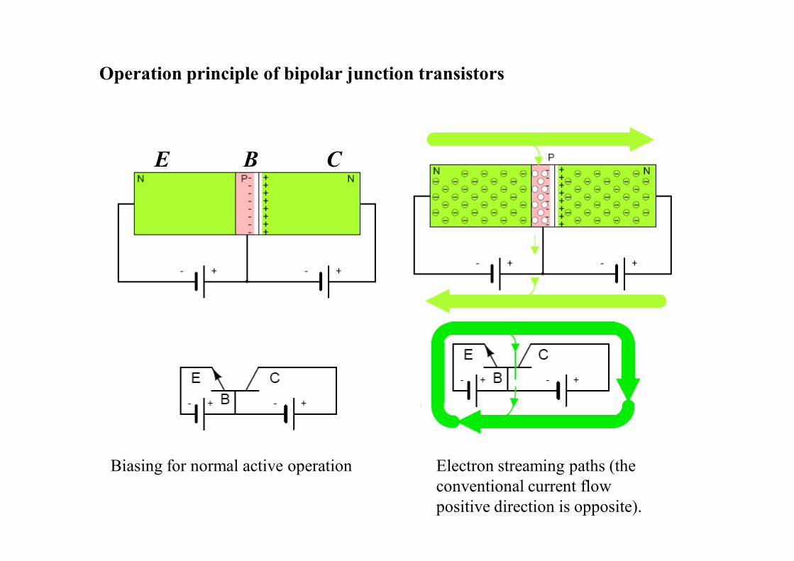
Operation principle of bipolar junction transistors
Electron streaming paths (the conventional current flow positive direction is opposite).
Biasing for normal active operation
E B C
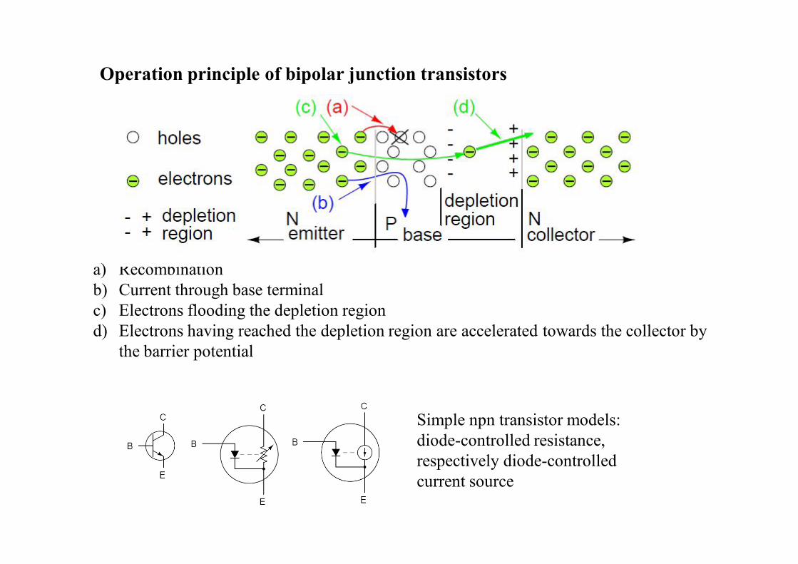
a) Recombinationb) Current through base terminalc) Electrons flooding the depletion regiond) Electrons having reached the depletion region are accelerated towards the collector by
the barrier potential
Operation principle of bipolar junction transistors
Simple npn transistor models: diode-controlled resistance, respectively diode-controlled current source
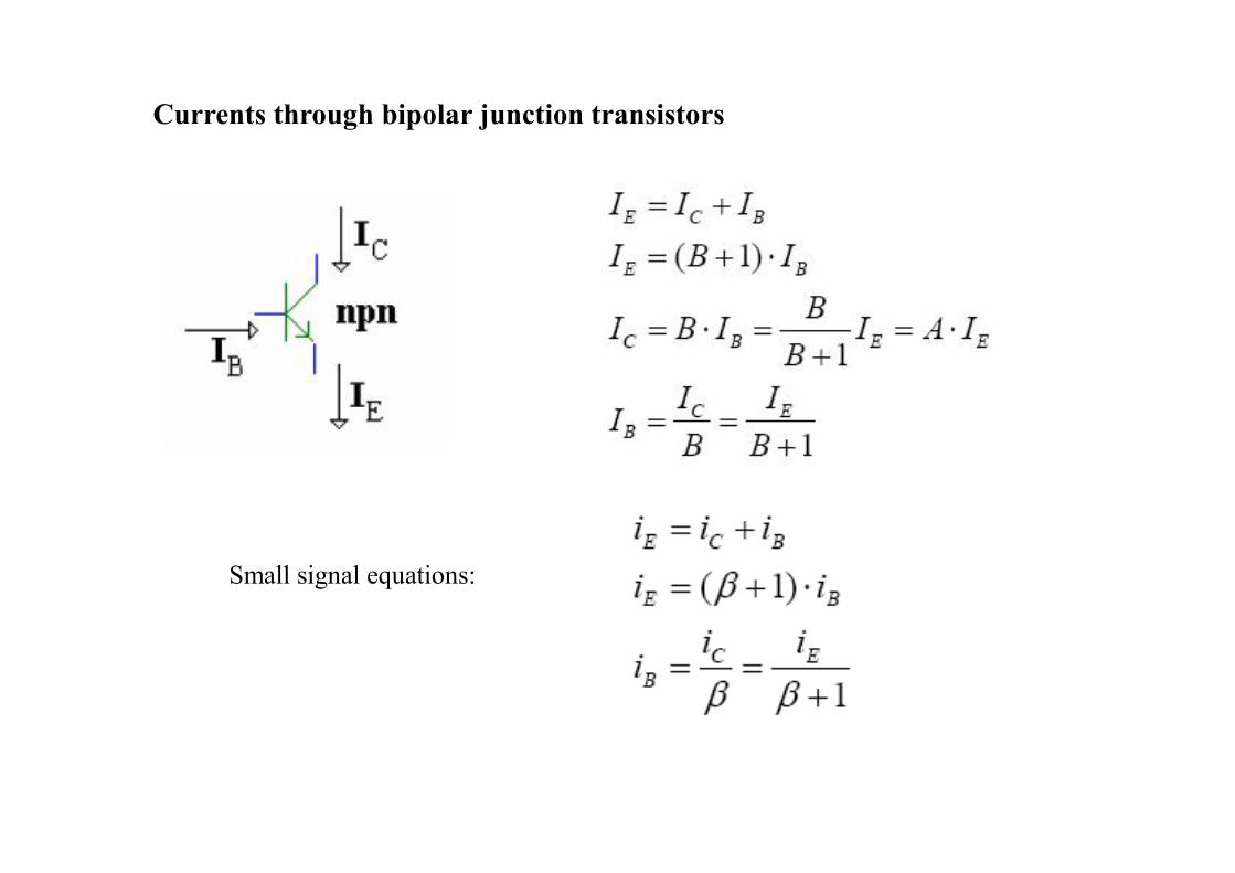
Currents through bipolar junction transistors
Small signal equations:
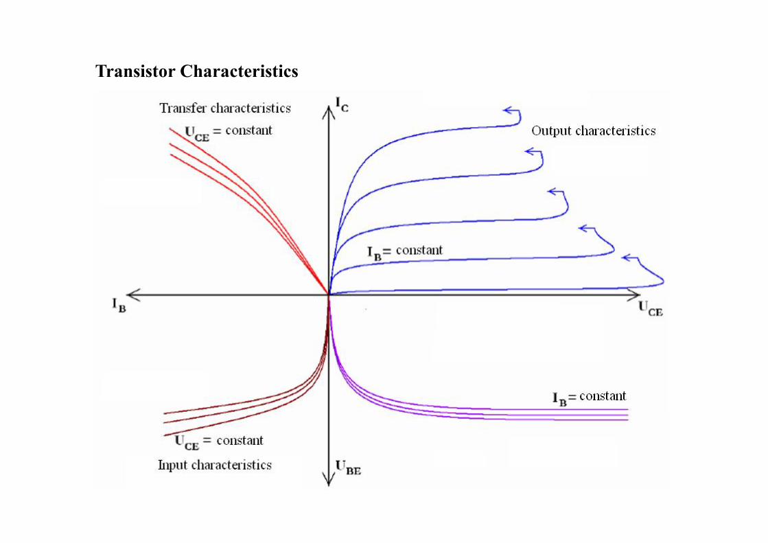
Transistor Characteristics
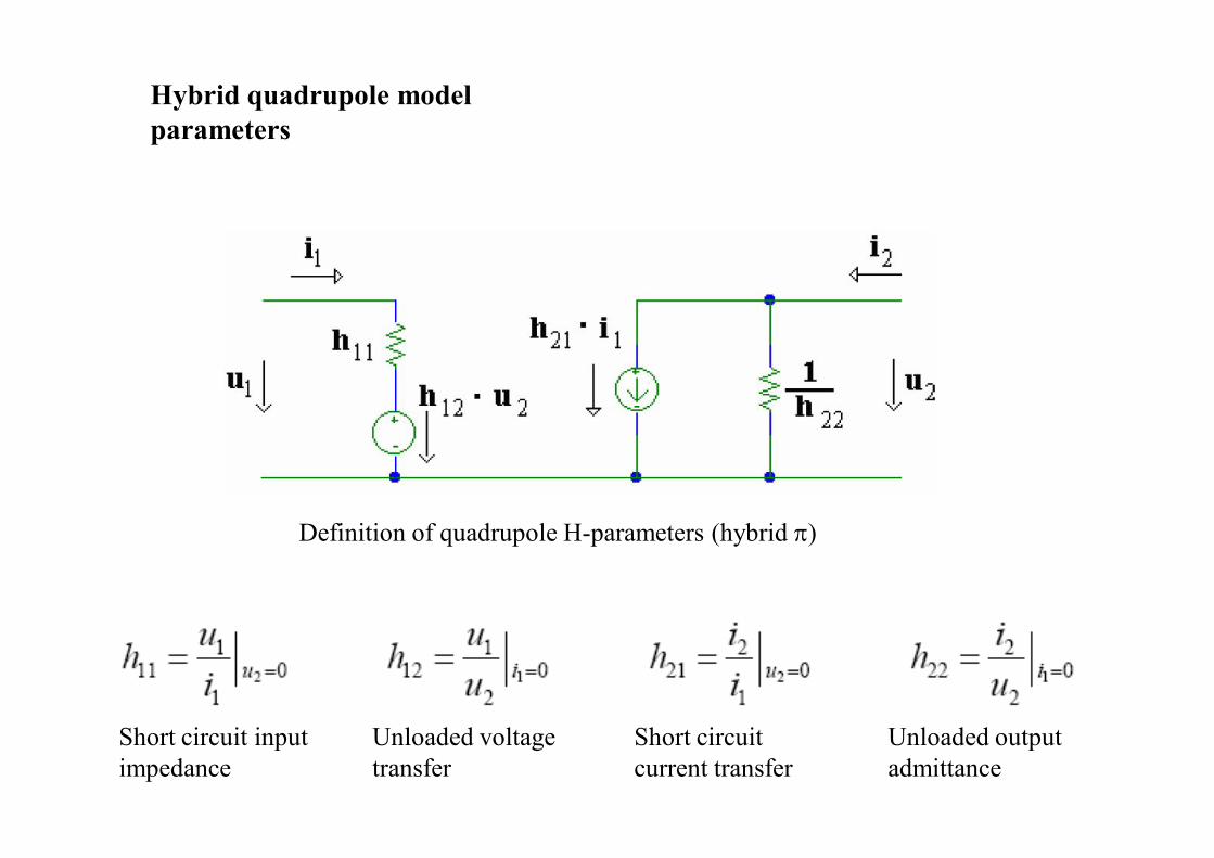
Hybrid quadrupole model parameters
Definition of quadrupole H-parameters (hybrid p)
Short circuit input impedance
Unloaded voltage transfer
Short circuit current transfer
Unloaded output admittance
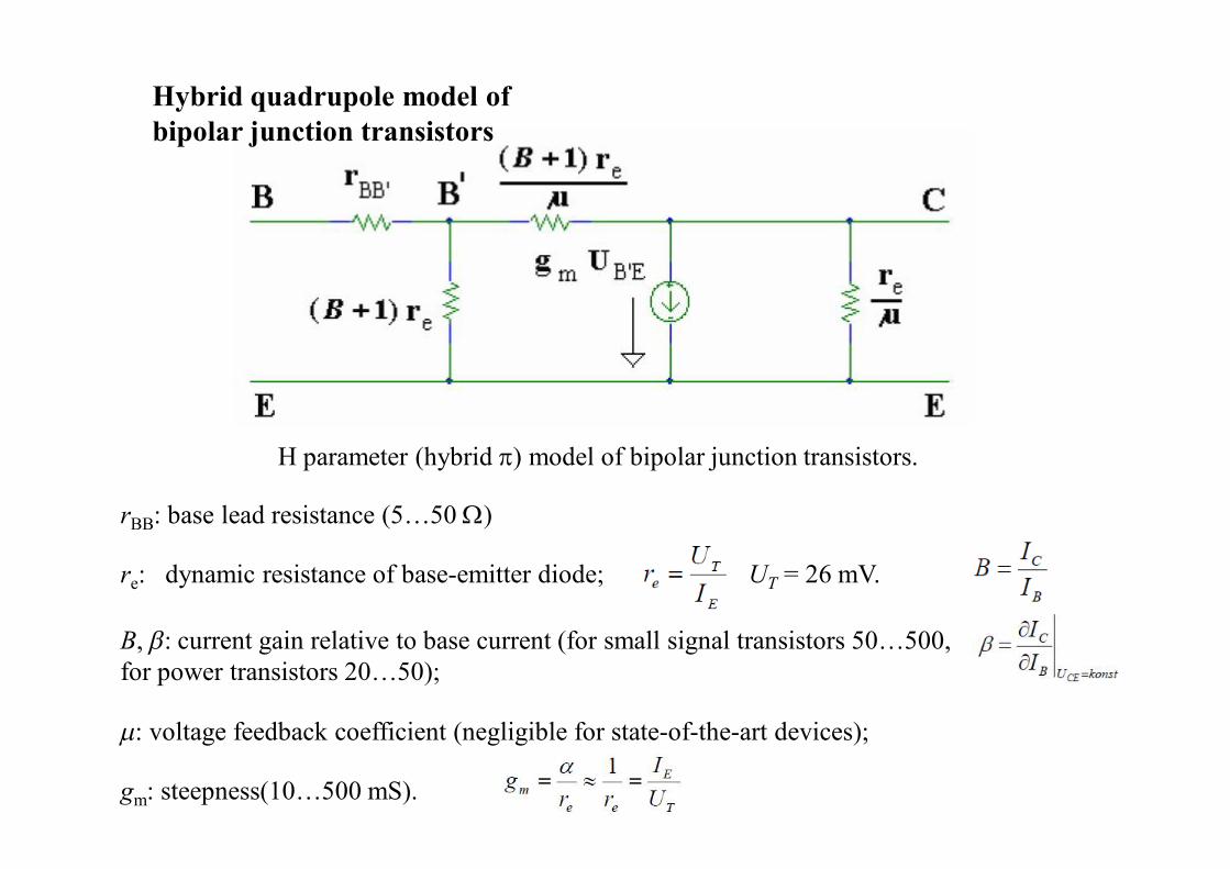
H parameter (hybrid p) model of bipolar junction transistors.
rBB: base lead resistance (5…50 W)
re: dynamic resistance of base-emitter diode; UT = 26 mV.
B, b: current gain relative to base current (for small signal transistors 50…500, for power transistors 20…50);
m: voltage feedback coefficient (negligible for state-of-the-art devices);
gm: steepness(10…500 mS).
Hybrid quadrupole model of bipolar junction transistors
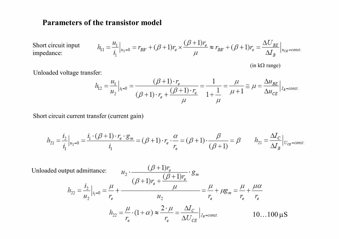
Parameters of the transistor model
10…100 mS
Short circuit input impedance:
Unloaded voltage transfer:
Unloaded output admittance:
Short circuit current transfer (current gain)
(in kW range)
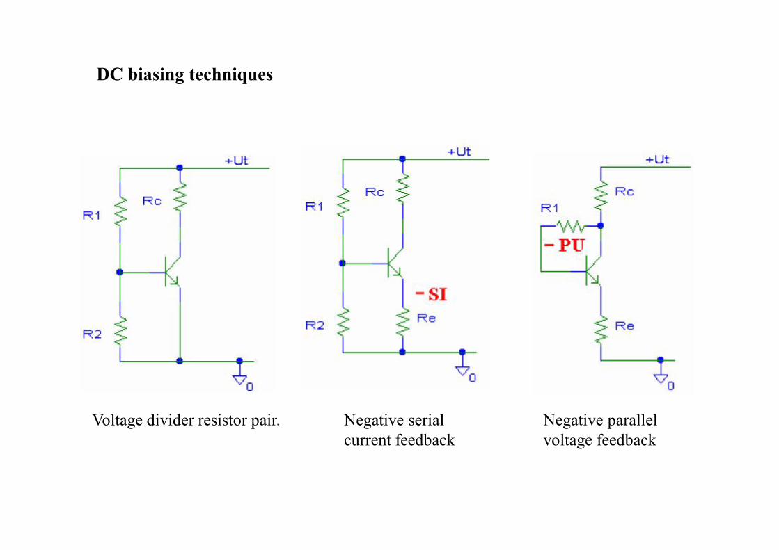
DC biasing techniques
Voltage divider resistor pair. Negative serial current feedback
Negative parallel voltage feedback
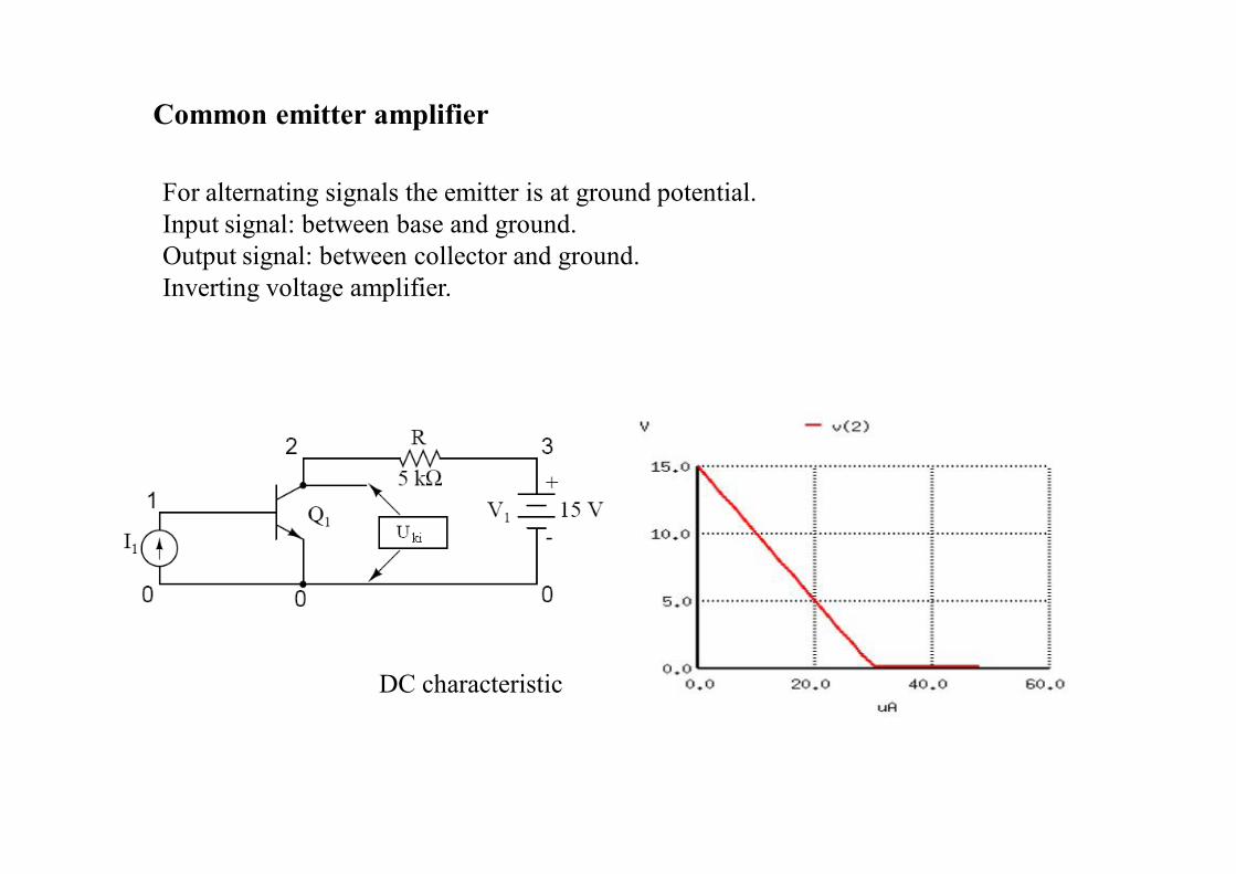
Common emitter amplifier
For alternating signals the emitter is at ground potential.Input signal: between base and ground.Output signal: between collector and ground.Inverting voltage amplifier.
DC characteristic
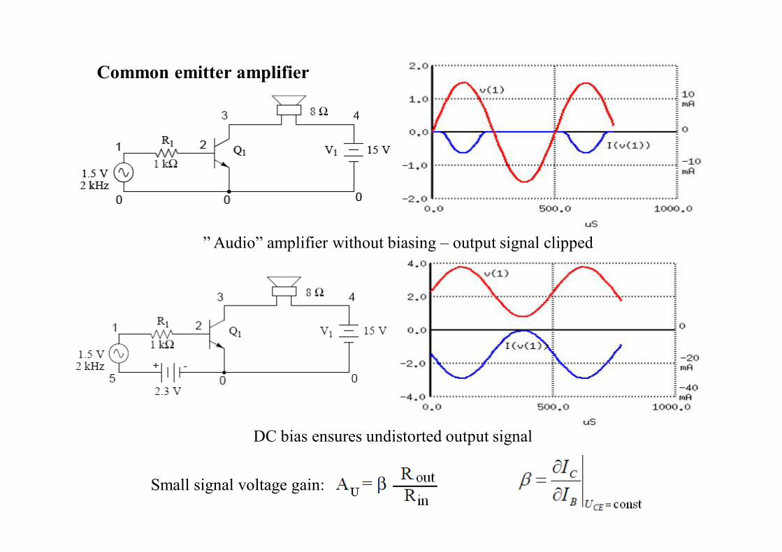
Common emitter amplifier
” Audio” amplifier without biasing – output signal clipped
DC bias ensures undistorted output signal
Small signal voltage gain:
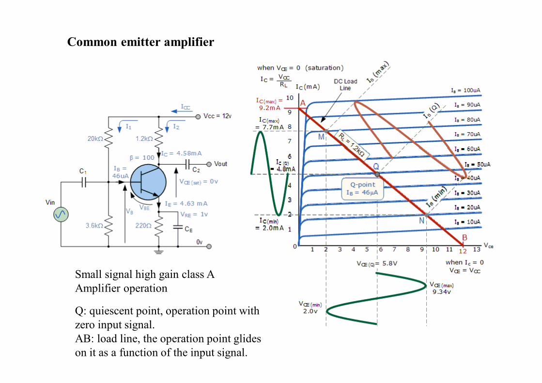
Common emitter amplifier
Small signal high gain class AAmplifier operation
Q: quiescent point, operation point with zero input signal.AB: load line, the operation point glides on it as a function of the input signal.
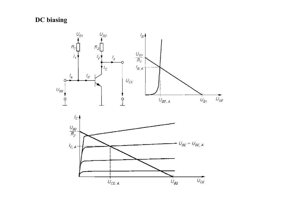
DC biasing
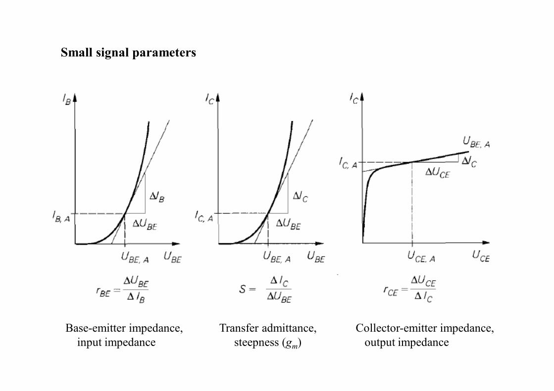
Small signal parameters
Base-emitter impedance, Transfer admittance, Collector-emitter impedance,input impedance steepness (gm) output impedance
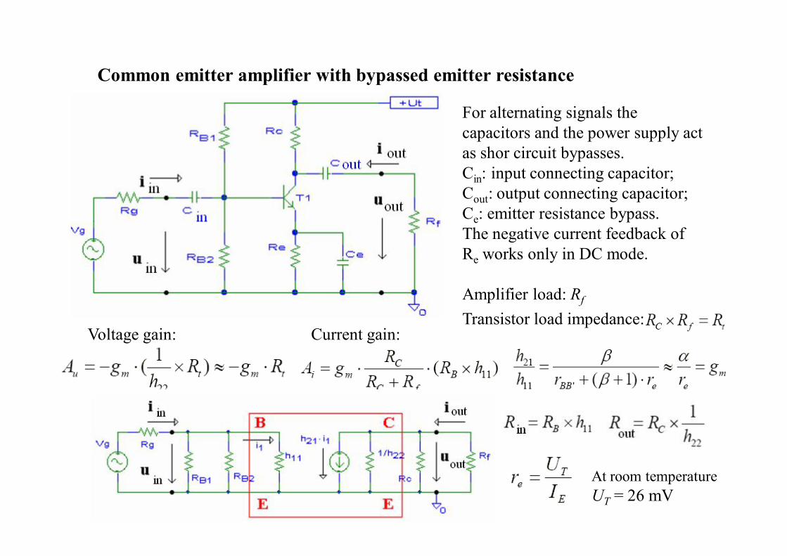
Common emitter amplifier with bypassed emitter resistance
Voltage gain: Current gain:
For alternating signals the capacitors and the power supply act as shor circuit bypasses.Cin: input connecting capacitor;Cout: output connecting capacitor;Ce: emitter resistance bypass.The negative current feedback of Re works only in DC mode.
Amplifier load: RfTransistor load impedance:
At room temperatureUT = 26 mV
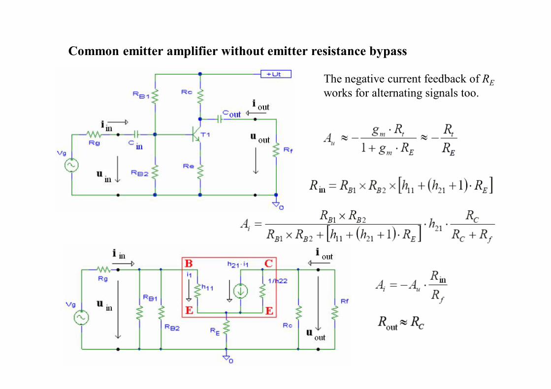
Common emitter amplifier without emitter resistance bypass
The negative current feedback of REworks for alternating signals too.
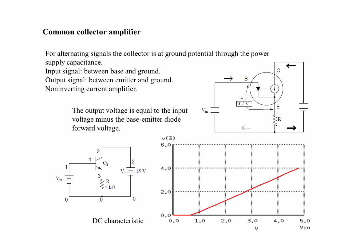
Common collector amplifier
For alternating signals the collector is at ground potential through the power supply capacitance.Input signal: between base and ground.Output signal: between emitter and ground.Noninverting current amplifier.
DC characteristic
The output voltage is equal to the input voltage minus the base-emitter diode forward voltage.
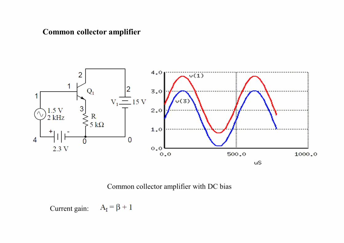
Common collector amplifier
Current gain:
Common collector amplifier with DC bias
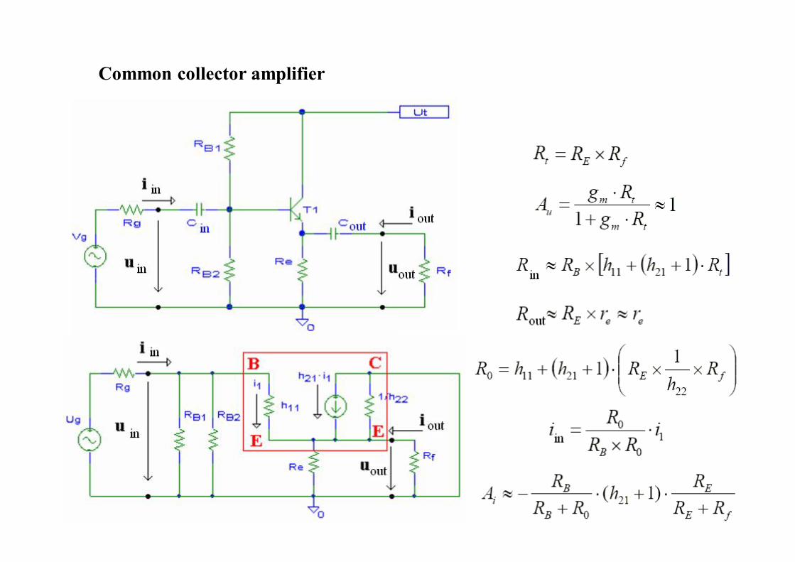
Common collector amplifier
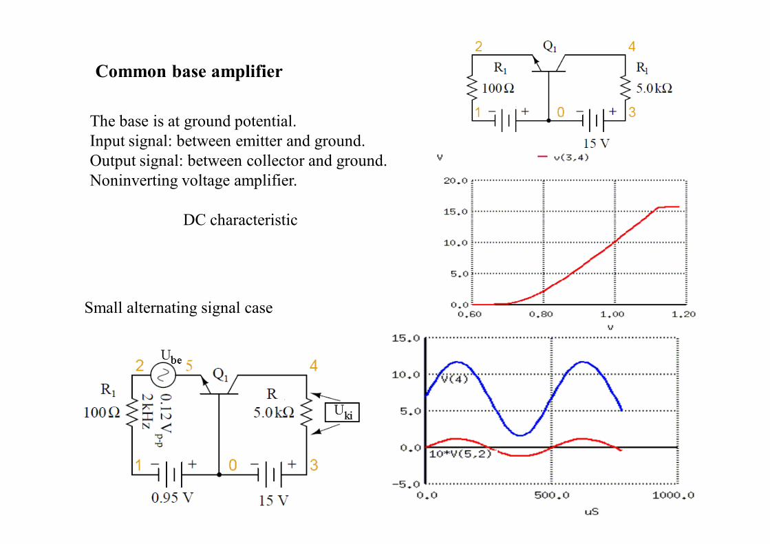
Common base amplifier
Small alternating signal case
The base is at ground potential.Input signal: between emitter and ground.Output signal: between collector and ground.Noninverting voltage amplifier.
DC characteristic
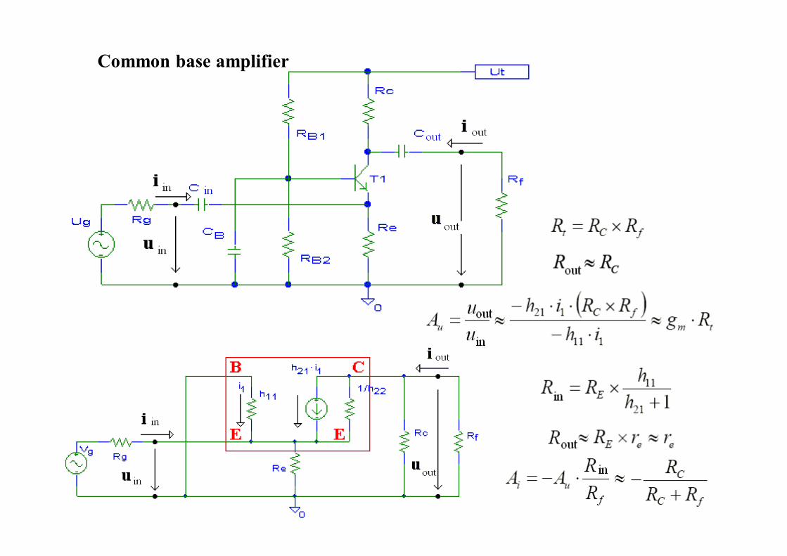
Common base amplifier
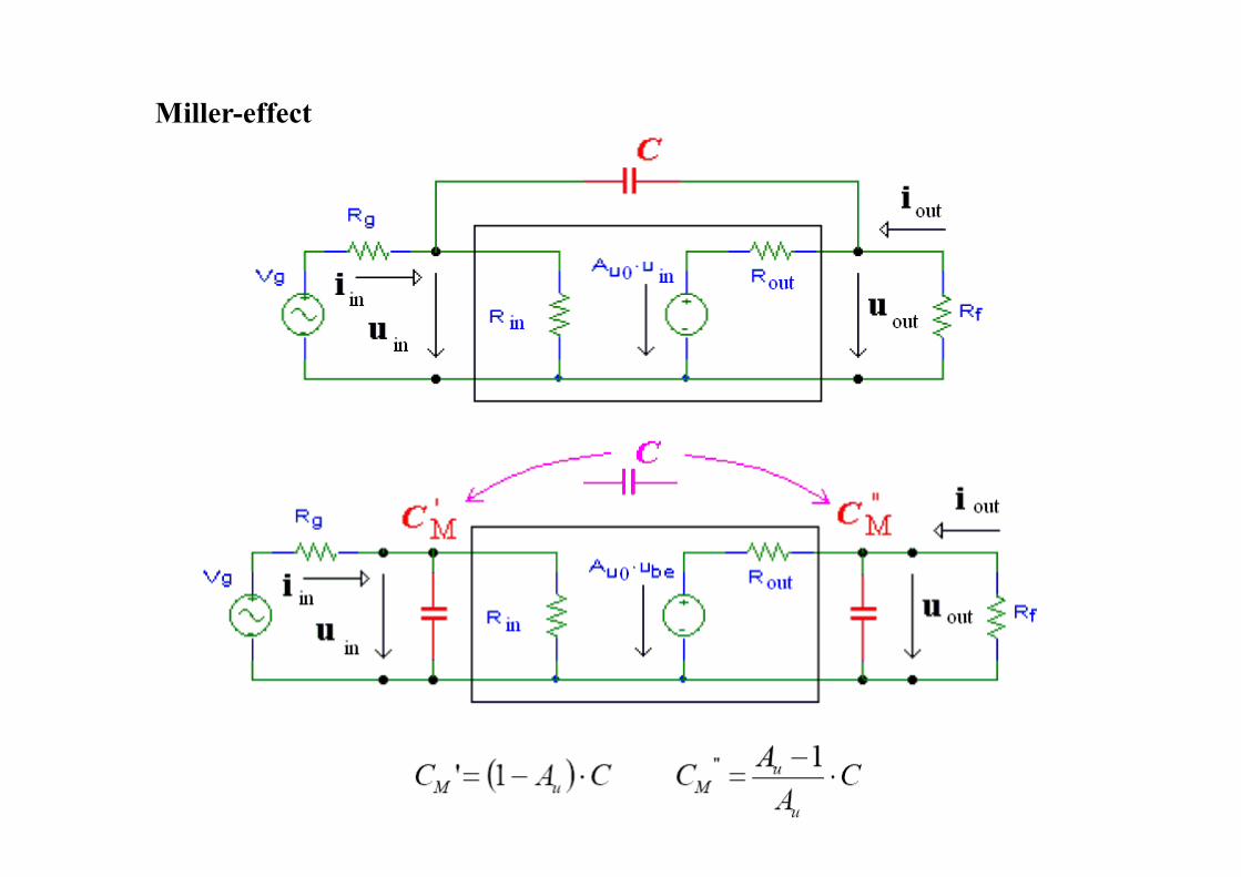
Miller-effect
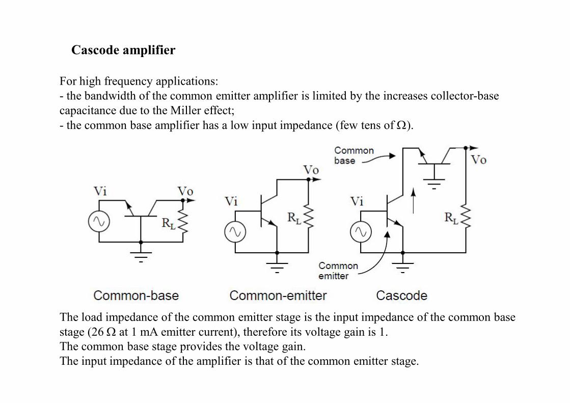
Cascode amplifier
For high frequency applications:- the bandwidth of the common emitter amplifier is limited by the increases collector-base capacitance due to the Miller effect;- the common base amplifier has a low input impedance (few tens of W).
Földelt bázisú Földelt emitteres Kaszkód
The load impedance of the common emitter stage is the input impedance of the common base stage (26 W at 1 mA emitter current), therefore its voltage gain is 1.The common base stage provides the voltage gain.The input impedance of the amplifier is that of the common emitter stage.
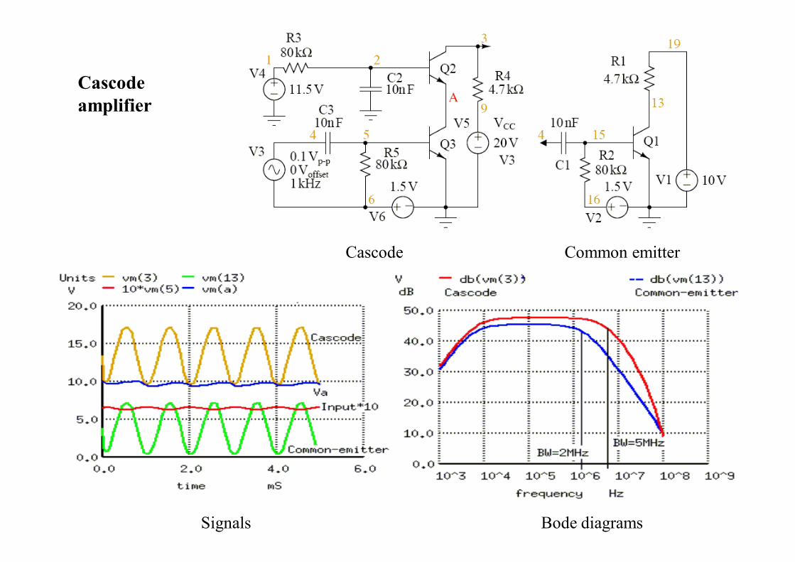
Cascode amplifier
Cascode Common emitter
Signals Bode diagrams
Related Documents