POUR L'OBTENTION DU GRADE DE DOCTEUR ÈS SCIENCES acceptée sur proposition du jury: Prof. R. Houdré, président du jury Prof. O. Yazyev, directeur de thèse Dr J. Fernández-Rossier, rapporteur Prof. J. Fabian, rapporteur Prof. A. Kis, rapporteur Electronic Transport in 2D Materials with Strong Spin-orbit Coupling THÈSE N O 7390 (2017) ÉCOLE POLYTECHNIQUE FÉDÉRALE DE LAUSANNE PRÉSENTÉE LE 10 MARS 2017 À LA FACULTÉ SCIENCES DE BASE CHAIRE DE PHYSIQUE NUMÉRIQUE DE LA MATIÈRE CONDENSÉE PROGRAMME DOCTORAL EN PHYSIQUE Suisse 2017 PAR Artem PULKIN

Welcome message from author
This document is posted to help you gain knowledge. Please leave a comment to let me know what you think about it! Share it to your friends and learn new things together.
Transcript

POUR L'OBTENTION DU GRADE DE DOCTEUR ÈS SCIENCES
acceptée sur proposition du jury:
Prof. R. Houdré, président du juryProf. O. Yazyev, directeur de thèse
Dr J. Fernández-Rossier, rapporteurProf. J. Fabian, rapporteur
Prof. A. Kis, rapporteur
Electronic Transport in 2D Materialswith Strong Spin-orbit Coupling
THÈSE NO 7390 (2017)
ÉCOLE POLYTECHNIQUE FÉDÉRALE DE LAUSANNE
PRÉSENTÉE LE 10 MARS 2017
À LA FACULTÉ SCIENCES DE BASECHAIRE DE PHYSIQUE NUMÉRIQUE DE LA MATIÈRE CONDENSÉE
PROGRAMME DOCTORAL EN PHYSIQUE
Suisse2017
PAR
Artem PULKIN

AbstractThe thesis describes the computational study of structural, electonic and transport properties
of monolayer transition metal dichalcogenides (TMDs) in the stable 2H and the metastable
1T’ phases. Several aspects have been covered by the study including the electronic properties
of the topological quantum spin Hall (QSH) state in the 1T’ monolayer phase as well as the
effects of strain, periodic line defects, interfaces and edges of monolayer TMDs. The electronic
properties of the bulk monolayer phases were described by the ab-initio density functional
theory (DFT) framework while the electronic and transport properties of 1D defects were
calculated using the non-equilibrium Green’s function (NEGF) formalism and its extensions.
A specific focus was made on the transport of spin-polarized charge carriers across line defects
in the monolayer 2H phase. Subject to energy, pseudomomentum and spin conservation, the
size of the transport gap is governed by both bulk properties of a material and symmetries of
a line defect. Outside the transport gap energy region, the charge carriers are discriminated
with respect to their spin resulting in the spin polarization of the transmitted current.
Next, the properties of the metastable monolayer 1T’ phase, its edges and interfaces with the
2H structural phase were studied. The presence of a sufficiently large band gap is important
for the observation of the QSH phase in the family of materials by probing the topologically
protected boundary states. The meV-order band gaps of the 1T’ phase of monolayer TMDs
were found to be sensitive to materials’ lattice constants suggesting the control of the band gap
size by strain. In particular, the electronic band structure and the size of the band gap in mono-
layer 1T’-WSe2 were found to be in agreement with experimental spectroscopy studies. The
topologically protected states at the edges of the monolayer 1T’ phase as well as at the bound-
aries between the topological 1T’ phase and the trivial 2H phase of monolayer TMDs were
studied. The dispersion of edge bands depends on the atomic structure of the boundary/ter-
mination. Specific atomic structure configurations were suggested to observe experimentally
the topological protection of the charge carrier transport against back-scattering.
Finally, in the context of lateral semiconducting device engineering, the electronic and trans-
verse transport properties of phase boundaries between the 2H and the 1T’ phases as well as
the dimerization defects in the 1T’ phase were investigated. Both kinds of defects considered
exhibit a relatively large transmission probability for the charge carriers crossing the defects.
However, the differences between the shapes of bulk bands of the two phases open a sizeable
transport gap for charge carriers crossing periodic domain boundaries between the monolayer
2H and 1T’ phases. The calculated formation energies of dimerization defects were found to
be relatively low suggesting their high concentration in real samples of monolayer 1T’-TMDs.
i

Additionally, the thesis includes studies of magnetic dopants on the surface of Bi2Te3 and
atomic vacancies in monolayer 2H-MoSe2 where the electronic properties of point defects
were calculated and compared to experimental results. The two possible adsorption sites of
Fe on the surface of Bi2Te3 both show a large out-of-plane magnetic anisotropy in agreement
with experiments. The calculated local electronic properties of Se vacancies in monolayer 2H-
MoSe2 show the presence of in-gap states which are not observed in experiment. Nevertheless,
the combination of theoretical and experimental scanning tunneling microscopy images
allowed the unambiguous identification of the vacancy defect.
Keywords: 2D materials, transition metal dichalcogenides, TMDs, line defects, domain bound-
aries, spin-orbit coupling, density functional theory, ballistic transport, non-equilibrium
Green’s function, NEGF, spin current, quantum spin Hall effect, QSH, topological insulators.
ii

RésuméCette thèse décrit l’étude computationnelle des propriétés structurelles, électroniques et de
transport des dichalcogénures de métaux de transition (TMDs) monocouches, tant dans
la phase stable 2H que dans la phase métastable 1T’. Plusieurs aspects ont été couverts en
étudiant les propriétés électroniques dans l’état topologique de l’effet Hall quantique de
spin (QSH) dans la phase 1T’ monocouche, ainsi que l’effet de la pression, de défauts de
ligne périodiques, d’interfaces et d’effets de bord. Les propriétés électroniques des phases
immaculées ont été décrites par la théorie ab-initio de la fonctionnelle de la densité (DFT),
alors que les propriétés électroniques et de transport des défauts 1D ont été calculées à l’aide
du formalisme des fonctions de Green hors équilibre (NEGF) et ses extensions.
Une attention particulière a été portée au transport de porteurs de charge polarisés de spin
au travers de défauts de ligne dans la phase 2H monocouche. Sujette à la conservation de
l’énergie, du pseudo-moment et du spin, la taille du gap de transport est gouvernée à la fois
par les propriétés de la phase immaculée que par les symétries du défaut de ligne. En-dehors
de la région d’énergie du gap de transport, les porteurs de charge sont discriminés par rapport
à leur spin, résultant en une polarisation de spin du courant transmis.
Ensuite, les propriétés de la phase métastable 1T’, ses bords et interfaces avec la phase structu-
relle 2H ont été étudiées. La présence d’une bande interdite suffisamment large est importante
pour l’observation de la phase QSH dans cette famille de matériaux en sondant les états
de bord topologiquement protégés. Les bandes interdites de l’ordre de quelques meV de la
phase 1T’ des TMDs monocouches se sont révélés être sensibles aux constantes de réseau des
matériaux, suggérant un contrôle de la taille de la bande interdite par des effets de pression.
En particulier, la structure de bandes électronique et la taille de la bande interdite dans la
monocouche du matériau 1T’-WSe2 calculés sont en bonne correspondance avec des études
expérimentales de spectroscopie. Les états topologiquement protégés localisés sur les bords
dans la phase 1T’ monocouche, ainsi qu’à l’interface avec la phase triviale 2H, ont été étu-
diés. La dispersion des bandes de bord dépend de la structure atomique à la terminaison et
l’interface, respectivement. Des configurations atomiques spécifiques ont été suggérées afin
d’observer expérimentalement la protection topologique des porteurs de charge contre la
rétrodiffusion.
Finalement, dans le contexte d’ingénierie de dispositif latéraux semi-conducteurs, les proprié-
tés électroniques et de transport de frontières entre les phases 2H et 1T’, ainsi que des effets de
défaut de dimérisation dans la phase 1T’, ont été étudiées. Les deux types de défaut considérés
ont révélé comporter une haute probabilité de transmission pour les porteurs de charge à
iii

travers les défauts. Cependant, les différences entre les formes des bandes dans les deux
phases ouvre un gap de transport de taille pour les porteurs de charge traversant les frontières
de phase périodiques entre les phases 2H et 1T’ monocouches. Les énergies de formation
calculées des défauts de dimérisation se sont révélées relativement petites, suggérant une
forte concentration dans des échantillons réels de monocouches de TMDs dans la phase 1T’.
En plus, cette thèse comporte des études de dopants magnétiques sur la surface du Bi2Te3 et de
vacances atomiques dans le 2H-MoS2 monochouche, où les propriétés de défauts ponctuels
ont été calculées et comparées avec des résultats expérimentaux. Les deux sites d’absorption
possible du Fe sur la surface de Bi2Te3 révèlent une forte anisotropie magnétique hors du
plan, en accord avec les expériences. Les propriétés électroniques locales de vacance de Se
dans le 2H-MoS2 monocouche révèlent la présence d’états dans la bande interdite qui ne sont
pas observés expérimentalement. Néanmoins, la combinaison théorique et expérimentale
d’images de microscopie à effet tunnel ont permis une identification non-ambiguë de la
vacance.
Mot clés : matériaux 2D, dichalcogénures de métaux de transition, TMDs, défauts de ligne,
limites de domaines, couplage spin-orbite, théorie de la fonctionnelle de la densité, transport
ballistique, fonctions de Green hors équilibre, NEGF, effet Hall quantique de spin, QSH, isolants
topologiques.
iv

ContentsAbstract (English/Français) i
List of figures vii
List of tables ix
1 Introduction 1
1.1 Modern electronics: successes and problems . . . . . . . . . . . . . . . . . . . . 1
1.2 Electron spin . . . . . . . . . . . . . . . . . . . . . . . . . . . . . . . . . . . . . . . . 2
1.3 Novel materials for applications in electronics . . . . . . . . . . . . . . . . . . . . 4
1.3.1 2D materials . . . . . . . . . . . . . . . . . . . . . . . . . . . . . . . . . . . . 5
1.3.2 Topological insulators . . . . . . . . . . . . . . . . . . . . . . . . . . . . . . 7
1.3.3 Defects in materials . . . . . . . . . . . . . . . . . . . . . . . . . . . . . . . 11
1.3.4 Charge carrier transport in solid state . . . . . . . . . . . . . . . . . . . . . 13
2 Methodology 17
2.1 Density functional theory (DFT) . . . . . . . . . . . . . . . . . . . . . . . . . . . . 17
2.1.1 Kohn-Sham equations . . . . . . . . . . . . . . . . . . . . . . . . . . . . . . 17
2.1.2 Limitations of DFT . . . . . . . . . . . . . . . . . . . . . . . . . . . . . . . . 18
2.1.3 DFT in crystals, the Bloch theorem and the Brillouin zone . . . . . . . . . 19
2.1.4 Core electrons and pseudopotentials . . . . . . . . . . . . . . . . . . . . . 23
2.1.5 Electron spin and spin-orbit coupling in DFT . . . . . . . . . . . . . . . . 24
2.1.6 Single-electron basis in DFT . . . . . . . . . . . . . . . . . . . . . . . . . . 26
2.2 Ballistic transport at nanoscale with DFT . . . . . . . . . . . . . . . . . . . . . . . 28
2.2.1 Green’s function formalism . . . . . . . . . . . . . . . . . . . . . . . . . . . 29
2.2.2 Transport of electron spin . . . . . . . . . . . . . . . . . . . . . . . . . . . . 44
2.2.3 Optimizing computational costs with the Green’s function method . . . 45
2.3 Simulating scanning tunneling microscopy (STM) images . . . . . . . . . . . . . 47
3 Spin and valley transport across regular line defects in semiconducting TMDs 51
3.1 Bulk properties of monolayer 2H-TMDs . . . . . . . . . . . . . . . . . . . . . . . . 52
3.2 Line defects in monolayer 2H-MoS2 and other TMDs . . . . . . . . . . . . . . . . 55
3.3 Ballistic transport across periodic line defects in a monolayer 2H-MoS2 . . . . . 57
3.3.1 The transport gap . . . . . . . . . . . . . . . . . . . . . . . . . . . . . . . . . 57
v
Contents
3.3.2 Transport simulations and the spin polarization of charge carrier current 60
3.4 Ballistic transport across inversion domain boundary in monolayer 2H-MoSe2 63
3.5 Conclusions . . . . . . . . . . . . . . . . . . . . . . . . . . . . . . . . . . . . . . . . 65
4 Electronic properties of the distorted 1T structural phase in monolayer TMDs 67
4.1 Bulk properties of the monolayer 1T’ phase . . . . . . . . . . . . . . . . . . . . . 68
4.1.1 Electronic structure properties of monolayer 1T’-WSe2 . . . . . . . . . . 70
4.1.2 Properties of monolayer 1T’-TMDs under strain . . . . . . . . . . . . . . . 72
4.1.3 Summary . . . . . . . . . . . . . . . . . . . . . . . . . . . . . . . . . . . . . . 76
4.2 Edges of monolayer 1T’-TMDs . . . . . . . . . . . . . . . . . . . . . . . . . . . . . 77
4.2.1 Summary . . . . . . . . . . . . . . . . . . . . . . . . . . . . . . . . . . . . . . 80
4.3 Electronic properties of structural phase boundaries in monolayer WSe2 . . . . 81
4.3.1 Summary . . . . . . . . . . . . . . . . . . . . . . . . . . . . . . . . . . . . . . 85
4.4 Electronic properties of dimerization defects in monolayer 1T’-WSe2 . . . . . . 86
4.4.1 Summary . . . . . . . . . . . . . . . . . . . . . . . . . . . . . . . . . . . . . . 89
4.5 Conclusions . . . . . . . . . . . . . . . . . . . . . . . . . . . . . . . . . . . . . . . . 90
5 Simulating STM images of point defects in spin-orbit systems 91
5.1 Magnetic adatoms on the surface of Bi2Te3 . . . . . . . . . . . . . . . . . . . . . . 91
5.1.1 Thermodynamical properties of adatoms . . . . . . . . . . . . . . . . . . . 93
5.1.2 Electronic and magnetic properties of adatoms . . . . . . . . . . . . . . . 93
5.1.3 Conclusions . . . . . . . . . . . . . . . . . . . . . . . . . . . . . . . . . . . . 95
5.2 Selenium vacancies in monolayer 2H-MoSe2 . . . . . . . . . . . . . . . . . . . . . 95
5.2.1 Electronic properties of Se vacancies . . . . . . . . . . . . . . . . . . . . . 97
5.2.2 Conclusions . . . . . . . . . . . . . . . . . . . . . . . . . . . . . . . . . . . . 97
6 Outlook 101
A Appendix 103
A.1 On left and right eigenvalues . . . . . . . . . . . . . . . . . . . . . . . . . . . . . . 103
A.2 Valley filtering with line defects . . . . . . . . . . . . . . . . . . . . . . . . . . . . . 104
A.3 Simulation details: charge carrier transport in monolayer 2H-MoS2 . . . . . . . 106
A.4 Simulation details: spin polarization of the transmission probability in mono-
layer 2H-MoS2 . . . . . . . . . . . . . . . . . . . . . . . . . . . . . . . . . . . . . . . 107
A.5 Projected band structure in MoS2 and other TMDs . . . . . . . . . . . . . . . . . 110
A.6 Simulation details: periodic zigzag terminations of monolayer 1T’-TMDs . . . . 112
A.7 Local densities of states at the zigzag terminations of monolayer 1T’-TMDs . . 113
A.8 Simulation details: Fe adatoms on the surface of Bi2Te3 . . . . . . . . . . . . . . 113
A.9 Simulation details: point defects in MoSe2 . . . . . . . . . . . . . . . . . . . . . . 113
Bibliography 124
Curriculum Vitae 125
vi

List of Figures1.1 An example of an integrated circuit: TL431 voltage regulator . . . . . . . . . . . 3
1.2 A next-generation integrated circuit prepared from a bilayer MoS2 . . . . . . . . 4
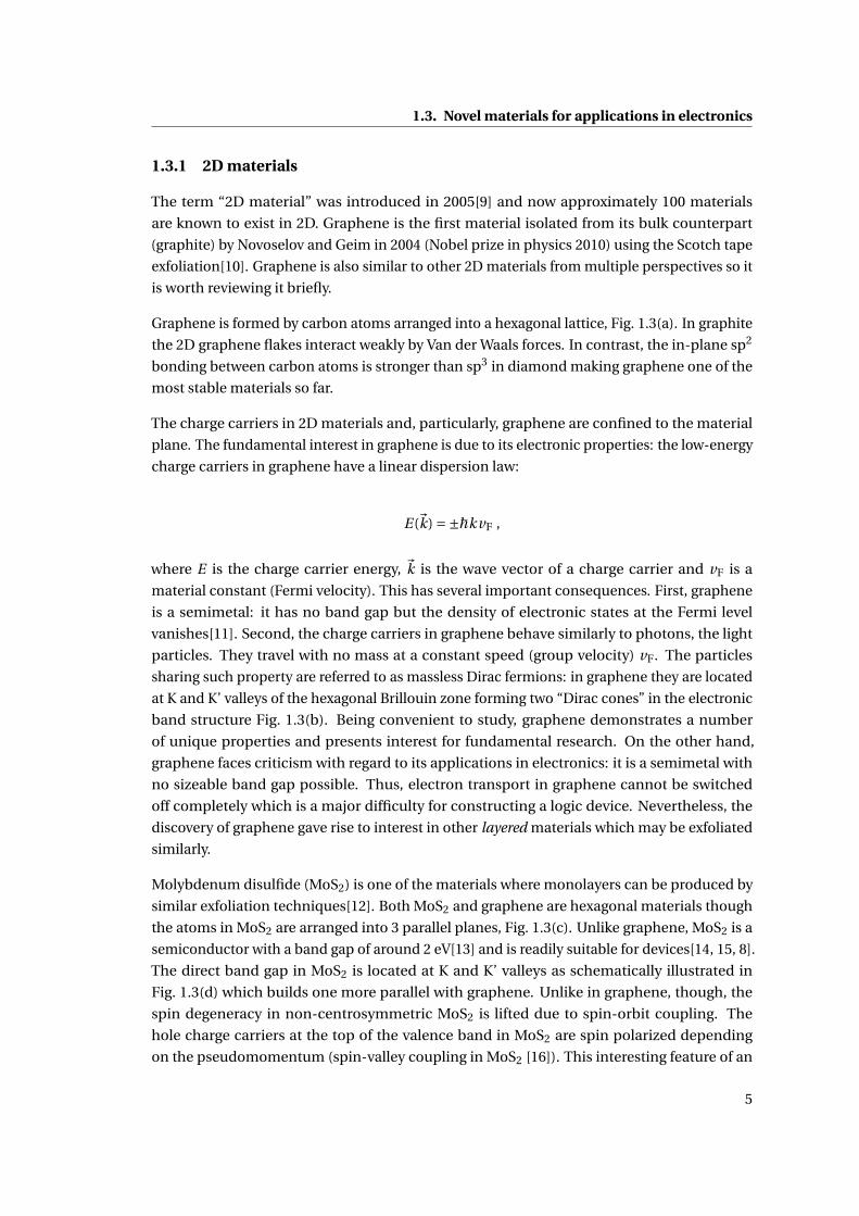
1.3 Atomic and electronic structures of 2D materials . . . . . . . . . . . . . . . . . . 6
1.4 Representatives of 2D materials . . . . . . . . . . . . . . . . . . . . . . . . . . . . 7
1.5 Band structures of the quantum spin Hall phase and the topologically trivial
phase of the Kane-Mele model . . . . . . . . . . . . . . . . . . . . . . . . . . . . . 8
1.6 Torus enclosing the origin point (black) as an illustration to topologically non-
trivial Bloch Hamiltonian . . . . . . . . . . . . . . . . . . . . . . . . . . . . . . . . 10
1.7 Models of line defects in MoS2 . . . . . . . . . . . . . . . . . . . . . . . . . . . . . 13
1.8 Defects observed in MoS2 . . . . . . . . . . . . . . . . . . . . . . . . . . . . . . . . 14
2.1 The periodic reciprocal space for a 2D hexagonal lattice . . . . . . . . . . . . . . 22
2.2 A sketch of a pseudopotential used in density functional theory simulations . . 25
2.3 A schematic illustration of a two-terminal ballistic transport setup . . . . . . . . 28
2.4 Ideal and defective 2D systems . . . . . . . . . . . . . . . . . . . . . . . . . . . . . 30
2.5 Structure of a nanowire device Hamiltonian . . . . . . . . . . . . . . . . . . . . . 32
2.6 Boundary conditions and unknown amplitudes in the transport setup . . . . . 36
2.7 A supercell model for the transport calculations . . . . . . . . . . . . . . . . . . . 46
3.1 The crystal structure and symmetries of monolayer 2H-TMDs . . . . . . . . . . 53
3.2 Electronic band structures of 6 2D TMDs. The electronic band gap Eg and the
largest spin-orbit splitting in the valence band ∆ are indicated in each case. . . 54
3.3 Fermi surfaces in monolayer 2H-MoS2 . . . . . . . . . . . . . . . . . . . . . . . . 55
3.4 Atomic structures of periodic line defects in monolayer 2H-MoS2 . . . . . . . . 56
3.5 The transport gap in a monolayer 2H-MoS2 . . . . . . . . . . . . . . . . . . . . . 58
3.6 A schematic illustration of bulk states of a monolayer 2H-MoS2 in the leads
projected onto the 1D BZ of the defect . . . . . . . . . . . . . . . . . . . . . . . . . 59
3.7 Transport properties across line defects in monolayer 2H-MoS2 . . . . . . . . . 61
3.8 The single-particle Hartree potential of monolayer 2H-MoS2 defects . . . . . . 62
3.9 Atomic microscopy images of defective monolayer 2H-MoSe2 . . . . . . . . . . 64
3.10 Electronic and transport properties of an inversion domain boundary in MoSe2 64
4.1 Structural phases of 2D TMDs: 2H, 1T and 1T’ . . . . . . . . . . . . . . . . . . . . 68
4.2 Electronic band structures of monolayer 1T’-TMDs . . . . . . . . . . . . . . . . . 69
vii
List of Figures
4.3 Electron and hole pockets in semimetallic monolayer 1T’-TMDs . . . . . . . . . 70
4.4 Experimental observation of the monolayer 1T’ phase in WSe2 . . . . . . . . . . 71
4.5 Evolution of the electronic properties of monolayer 1T’-TMDs upon the change
of lattice parameters . . . . . . . . . . . . . . . . . . . . . . . . . . . . . . . . . . . 74
4.6 The location of the conduction band minimum (CBM) in the Brillouin zone of
monolayer 1T’-TMDs as a function of lattice parameters . . . . . . . . . . . . . . 75
4.7 The topological invariant phase in strained monolayer 1T’-TMDs . . . . . . . . 76
4.8 Atomic structures of zigzag terminations in monolayer 1T’-TMDs and their
formation energies . . . . . . . . . . . . . . . . . . . . . . . . . . . . . . . . . . . . 78
4.9 The k-resolved density of states localized at the energetically preferred zigzag
terminations of monolayer 1T’-TMDs . . . . . . . . . . . . . . . . . . . . . . . . . 79
4.10 Momentum-resolved localized density of electronic states of zigzag terminations
suitable for the protected charge carrier ballistic transport experiment . . . . . 80
4.11 Atomic structures of the 2H-1T’ phase boundaries along the zigzag direction of
monolayer WSe2 . . . . . . . . . . . . . . . . . . . . . . . . . . . . . . . . . . . . . 82
4.12 Electronic structure of phase boundaries in monolayer WSe2 . . . . . . . . . . . 83
4.13 Charge carrier transmission function of the 2H-1T’ phase boundaries in mono-
layer WSe2 . . . . . . . . . . . . . . . . . . . . . . . . . . . . . . . . . . . . . . . . . 85
4.14 Relative transmissions of phase boundaries in WSe2 . . . . . . . . . . . . . . . . 86
4.15 Atomic structures of 1T’ periodic dimerization defects in monolayer WSe2 . . . 87
4.16 Electronic structure properties of dimerization defects in monolayer 1T’-WSe2 89
5.1 Fe dopants on the surface of Bi2Te3 . . . . . . . . . . . . . . . . . . . . . . . . . . 92
5.2 Electronic properties of Fe adatoms on the surface of Bi2Te3 . . . . . . . . . . . 94
5.3 Atomic structure and electronic properties of point defects in monolayer 2H-
MoSe2 . . . . . . . . . . . . . . . . . . . . . . . . . . . . . . . . . . . . . . . . . . . . 96
5.4 Density of electronic states for the selenium vacancy defect in monolayer 2H-
MoSe2 . . . . . . . . . . . . . . . . . . . . . . . . . . . . . . . . . . . . . . . . . . . . 98
5.5 STM images of the selenium vacancy in monolayer 2H-MoSe2: theory vs experi-
ment . . . . . . . . . . . . . . . . . . . . . . . . . . . . . . . . . . . . . . . . . . . . 99
A.1 A mirror-symmetric line defect in graphene . . . . . . . . . . . . . . . . . . . . . 105
A.2 An illustration of Fermi surfaces, branches and bulk states used in the calculation
of angle-dependent properties . . . . . . . . . . . . . . . . . . . . . . . . . . . . . 109
A.3 The local density of states of the six zigzag terminations presented in Fig. 4.8 . . 114
viii

List of Tables2.1 Basis sets: pros and cons . . . . . . . . . . . . . . . . . . . . . . . . . . . . . . . . . 27
3.1 Equilibrium lattice parameters a and h of monolayer 2H-TMDs (PBE-DFT level
of theory). . . . . . . . . . . . . . . . . . . . . . . . . . . . . . . . . . . . . . . . . . 52
4.1 Properties of a band gap in monolayer 1T’-TMDs . . . . . . . . . . . . . . . . . . 69
4.2 The magnitude of the transport gap for charge carriers propagating across phase
boundaries in monolayer WSe2 . . . . . . . . . . . . . . . . . . . . . . . . . . . . . 84
4.3 Formation energies of dimerization defects in monolayer 1T’-WSe2 . . . . . . . 88
5.1 Magnetic properties of Fe adatoms on the surface of Bi2Te3: magnetic moments
and anisotropies calculated by projecting occupied Bloch states onto atomic
orbitals. . . . . . . . . . . . . . . . . . . . . . . . . . . . . . . . . . . . . . . . . . . . 95
ix

1 Introduction
1.1 Modern electronics: successes and problems
Advances in modern technology are sometimes associated with the development of electronic
devices. They are built of electric circuits where currents serve a particular purpose: supply a
power for mechanical motion, light sources, heaters, etc. In the digital era a very simple idea
was developed: an electric current may carry information. The information is simply encoded
in the fact of the presence of the current: [switch is on = current flows = the bulb is lighted =
1] versus [switch is off = no current = the bulb is not lighted = 0]. The transfer of information
requires constantly switching circuits on and off done by electronic logic devices. Higher
switching speeds are reached by minimizing the power consumption of devices. The most
straightforward way to do it is to reduce the device size increasing resistances and reducing
currents according to Ohm’s law,
Resistance ∼ device length
section area.
Such approach and above law work well for ’classical’ devices larger than several nanometers
(nm, 1 nm = 10−9m) where electron is a classical particle (ball) having position and velocity.
At the time of writing this thesis (2016) this approach is almost depleted: the most advanced
consumer devices hit a feature size of 14 nm[1]. Thus, qualitatively new developments with
deeper understanding of electron properties are demanded.
Soon after discovering the electron particle (1897) it was realized that it behaves differently
in different materials. This led to a concept of an electronic structure of a solid material. Not
only the material itself but it’s temperature, impurities and defects influence the electronic
structure. This fact is widely used in modern silicon electronics where a single material
(Si) acts as a conductor (conducts electrons), an insulator (blocks electron transport) and
a semiconductor (switchable conductor). An example of a Si-based device is presented in
Fig. 1.1. There, different regions of Si have different roles resulting in a rather complicated
1

Chapter 1. Introduction
device consisting of multiple (up to 1010) blocks.
The bulk Si is, probably, the most studied material so far where the most important electronic
structure properties (the band gap magnitude and the charge carrier concentration) can be
varied precisely within certain ranges. On the other hand, the Si approaching 1 nm thickness
(or atomically thin Si) demonstrates completely different electronic properties[2] because
electrons become extremely confined along one of the dimensions. Thus, to be able to
compete with Si an insight is required into material properties in 2D.
While novel materials promise quantitative performance boost, the qualitative changes are
preferred. The last breakthrough in this field happened in 1947 with the invention of a solid-
state transistor[4] used till now. Researchers, however, discuss various possibilities to operate
information by using light or electron spin. This would not only raise existing performance
limits but also re-think of what information actually is: from binary representation (on/off)
one would have a quantum superposition of “on” and “off” states. Thus, existing algorith-
mic problems can be be solved in a completely different manner commonly referred to as
“quantum computing”. The basic building block of a quantum computer, electron spin, is
introduced in the following chapter.
1.2 Electron spin
While it is a well-known fact for the general public that an electron carries the electric charge,
it is a little bit less known about what electron spin is. Conventionally, spin is presented as
an arrow attached to electron and pointing upward or downward. Unlike charge, spin is an
additional degree of freedom of elementary particles: it creates a magnetic moment, thus, it
can be changed by magnetic field. A rigid definition is given in Ref. [5], for example:
Spin is an intrinsic form of angular momentum (vector) carried by elementary particles,
composite particles (hadrons), and atomic nuclei.
The size of the spin is the same across all particles of a given kind. Thus, elementary particles
are classfied by the magnitude of spin: fermions have half-integer spins (1/2 for electron) while
integer values of spin are attributed to bosons (1 for a photon). Fermions and bosons have
fundamentally different properties in terms of particle statistics and commutation relations in
quantum physics.
The most intriguing fact about spin is that it cannot be measured completely: quantum
mechanics prohibits such experiment. It is possible to project the spin onto arbitrary direction
and obtain its value (+1/2 or −1/2 for electron) with a well-defined quantum mechanical
probability. Such measurement necessarily changes the spin and destroys the initial quantum
mechanical state of an electron. This fact is widely used in quantum cryptography providing a
way to track eavesedropping.
2

1.2. Electron spin
Figure 1.1 – An example of an integrated circuit (IC): TL431 voltage regulator. (a) Photographsof IC inside a package as it appears in consumer electronic devices reproduced with permissionfrom Ref. [3]. (b) IC under microscope. The different tones of pink/purple denote silicon withdifferent doping. The light colors correspond to metallic coating acting as connector wires.The red labels specify basic building blocks of an IC: resistors, capacitors and transistors. (c)An equivalent scheme of the TL431 with the corresponding elements from (b).
As it is evident from the above, the idea of a spin (or, more general, a quantum mechanical
state) carrying information attracted a lot of attention and evolved into quantum computing[6].
There, primitive data types (integers, floats) and operations (sums, products) are replaced by
vectors and linear operators. Interestingly, quantum informatics already has its own appli-
cations without any proof of a sizeable “quantum computer” have been built. For example,
3

Chapter 1. Introduction
Figure 1.2 – A next-generation integrated circuit prepared from a bilayer MoS2. The chargecarrier channel thickness approaches 1 nm. The image is reproduced with permission fromRef. [8].
the Shor’s algorithm for factorization of numbers[7] demonstrated weaknesses of existing
cryptographic protocols and stimulated development of different algorithms.
The spin is being used in conventional electronics since 1951: the information stored on
magnetic tapes, floppy disks and hard disc drives is essentially a macroscopic magnetization
formed by electron spins. From the performance point of view it is more efficient to use a
single spin instead of magnetization. To be able to operate spin by all-electric means under
normal conditions suitable materials are desired.
1.3 Novel materials for applications in electronics
There is no simple answer to the question whether 2D or any other novel material are better
than the well-established silicon framework for electronics applications. It has been pointed
out, however, that Si is used to the maximum of its possibilities, thus, it has to be replaced by
another material. 2D materials are promising candidates which can be prepared relatively
easily and stacked on top of each other to form an electronic device (Fig. 1.2) similarly to
existing industrial protocols for Si.
4
1.3. Novel materials for applications in electronics
1.3.1 2D materials
The term “2D material” was introduced in 2005[9] and now approximately 100 materials
are known to exist in 2D. Graphene is the first material isolated from its bulk counterpart
(graphite) by Novoselov and Geim in 2004 (Nobel prize in physics 2010) using the Scotch tape
exfoliation[10]. Graphene is also similar to other 2D materials from multiple perspectives so it
is worth reviewing it briefly.
Graphene is formed by carbon atoms arranged into a hexagonal lattice, Fig. 1.3(a). In graphite
the 2D graphene flakes interact weakly by Van der Waals forces. In contrast, the in-plane sp2
bonding between carbon atoms is stronger than sp3 in diamond making graphene one of the
most stable materials so far.
The charge carriers in 2D materials and, particularly, graphene are confined to the material
plane. The fundamental interest in graphene is due to its electronic properties: the low-energy
charge carriers in graphene have a linear dispersion law:
E(~k) =±ħkvF ,
where E is the charge carrier energy, ~k is the wave vector of a charge carrier and vF is a
material constant (Fermi velocity). This has several important consequences. First, graphene
is a semimetal: it has no band gap but the density of electronic states at the Fermi level
vanishes[11]. Second, the charge carriers in graphene behave similarly to photons, the light
particles. They travel with no mass at a constant speed (group velocity) vF. The particles
sharing such property are referred to as massless Dirac fermions: in graphene they are located
at K and K’ valleys of the hexagonal Brillouin zone forming two “Dirac cones” in the electronic
band structure Fig. 1.3(b). Being convenient to study, graphene demonstrates a number
of unique properties and presents interest for fundamental research. On the other hand,
graphene faces criticism with regard to its applications in electronics: it is a semimetal with
no sizeable band gap possible. Thus, electron transport in graphene cannot be switched
off completely which is a major difficulty for constructing a logic device. Nevertheless, the
discovery of graphene gave rise to interest in other layered materials which may be exfoliated
similarly.
Molybdenum disulfide (MoS2) is one of the materials where monolayers can be produced by
similar exfoliation techniques[12]. Both MoS2 and graphene are hexagonal materials though
the atoms in MoS2 are arranged into 3 parallel planes, Fig. 1.3(c). Unlike graphene, MoS2 is a
semiconductor with a band gap of around 2 eV[13] and is readily suitable for devices[14, 15, 8].
The direct band gap in MoS2 is located at K and K’ valleys as schematically illustrated in
Fig. 1.3(d) which builds one more parallel with graphene. Unlike in graphene, though, the
spin degeneracy in non-centrosymmetric MoS2 is lifted due to spin-orbit coupling. The
hole charge carriers at the top of the valence band in MoS2 are spin polarized depending
on the pseudomomentum (spin-valley coupling in MoS2 [16]). This interesting feature of an
5

Chapter 1. Introduction
Figure 1.3 – Atomic and electronic structures of 2D materials. (a) Atomic structure of graphene.(b) Electronic band structure of graphene from Ref. [11]. The Dirac cones are located in thecorners of the hexagonal Brillouin zone. (c) Atomic structure of a monolayer molybdenumdisulfide. (d) Schematic illustration of the electronic band structure of a monolayer MoS2.The hexagon represents the Brillouin zone of MoS2. The color represents spin polarization ofelectrons (spin-up blue and spin-down red).
electronic band structure of MoS2 was confirmed by several optical experiments[17, 18, 19].
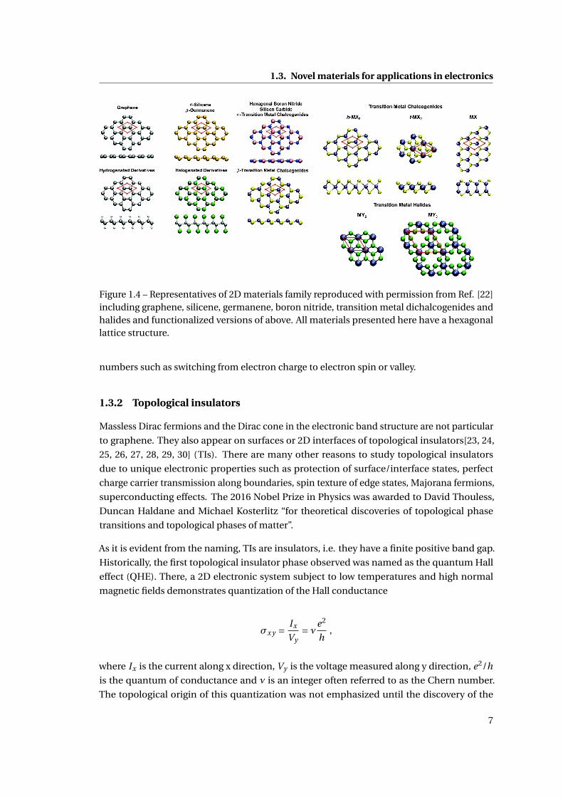
More 2D materials can be derived by using elements of the same atomic group. For example,
carbon, silicon and germanium belonging to group 14 form graphene, silicene and germanene
in Fig. 1.4. Similarly, molybdenum and tungsten from group 6 together with sulfur, selenium
and tellurium from group 16 form six transition metal dichalcogenides (TMDs). Inside each
group of materials the electronic properties differ mostly quantitatively. Apart from graphene
and MoS2, many other 2D materials have already been found suitable for electronic devices,
for example, WSe2 [20] and silicene[21]. Further developments in 2D material applications are
associated with conceptually new ways to encode information in the charge carrier quantum
6
1.3. Novel materials for applications in electronics
Figure 1.4 – Representatives of 2D materials family reproduced with permission from Ref. [22]including graphene, silicene, germanene, boron nitride, transition metal dichalcogenides andhalides and functionalized versions of above. All materials presented here have a hexagonallattice structure.
numbers such as switching from electron charge to electron spin or valley.
1.3.2 Topological insulators
Massless Dirac fermions and the Dirac cone in the electronic band structure are not particular
to graphene. They also appear on surfaces or 2D interfaces of topological insulators[23, 24,
25, 26, 27, 28, 29, 30] (TIs). There are many other reasons to study topological insulators
due to unique electronic properties such as protection of surface/interface states, perfect
charge carrier transmission along boundaries, spin texture of edge states, Majorana fermions,
superconducting effects. The 2016 Nobel Prize in Physics was awarded to David Thouless,
Duncan Haldane and Michael Kosterlitz “for theoretical discoveries of topological phase
transitions and topological phases of matter”.
As it is evident from the naming, TIs are insulators, i.e. they have a finite positive band gap.
Historically, the first topological insulator phase observed was named as the quantum Hall
effect (QHE). There, a 2D electronic system subject to low temperatures and high normal
magnetic fields demonstrates quantization of the Hall conductance
σx y = Ix
Vy= νe2
h,
where Ix is the current along x direction, Vy is the voltage measured along y direction, e2/h
is the quantum of conductance and ν is an integer often referred to as the Chern number.
The topological origin of this quantization was not emphasized until the discovery of the
7
Chapter 1. Introduction
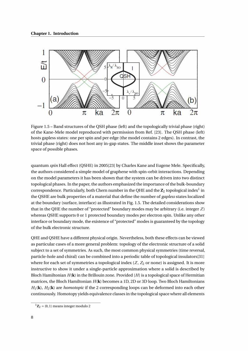
Figure 1.5 – Band structures of the QSH phase (left) and the topologically trivial phase (right)of the Kane-Mele model reproduced with permission from Ref. [23]. The QSH phase (left)hosts gapless states: one per spin and per edge (the model contains 2 edges). In contrast, thetrivial phase (right) does not host any in-gap states. The middle inset shows the parameterspace of possible phases.
quantum spin Hall effect (QSHE) in 2005[23] by Charles Kane and Eugene Mele. Specifically,
the authors considered a simple model of graphene with spin-orbit interactions. Depending
on the model parameters it has been shown that the system can be driven into two distinct
topological phases. In the paper, the authors emphasized the importance of the bulk-boundary
correspondence. Particularly, both Chern number in the QHE and the Z2 topological index1 in
the QSHE are bulk properties of a material that define the number of gapless states localized
at the boundary (surface, interface) as illustrated in Fig. 1.5. The detailed considerations show
that in the QHE the number of “protected” boundary modes may be arbitrary (i.e. integer Z )
whereas QSHE supports 0 or 1 protected boundary modes per electron spin. Unlike any other
interface or boundary mode, the existence of “protected” modes is guaranteed by the topology
of the bulk electronic structure.
QHE and QSHE have a different physical origin. Nevertheless, both these effects can be viewed
as particular cases of a more general problem: topology of the electronic structure of a solid
subject to a set of symmetries. As such, the most common physical symmetries (time reversal,
particle-hole and chiral) can be combined into a periodic table of topological insulators[31]
where for each set of symmetries a topological index (Z , Z2 or none) is assigned. It is more
instructive to show it under a single-particle approximation where a solid is described by
Bloch Hamiltonian H (k) in the Brillouin zone. Provided {H } is a topological space of Hermitian
matrices, the Bloch Hamiltonian H(k) becomes a 1D, 2D or 3D loop. Two Bloch Hamiltonians
H1(k), H2(k) are homotopic if the 2 corresponding loops can be deformed into each other
continuously. Homotopy yields equivalence classes in the topological space where all elements
1Z2 = {0,1} means integer modulo 2
8

1.3. Novel materials for applications in electronics
of the same class are topologically equivalent. Thus, it is possible to define a topological
invariant (Chern number, Z2 index, winding number, etc.) which is same for topologically
equivalent Hamiltonians and different for inequivalent ones. The number of classes roughly
characterizes the topological space: for example, only two classes exist for QSH Hamiltonians:
a trivial one and a non-trivial one. Conventionally, all Hamiltonians similar to the vacuum2
are assigned a trivial class.
As an instructive example of the topological characterization of Bloch Hamiltonians consider
a two-band tight-binding model. The most general way to write it is to use Pauli matrices
σx,y,z :
H(~k) = E0(~k)+ ∑i=x,y,z
hi (~k) ·σi . (1.1)
For simplicity, let’s assume that the energy origin E0(~k) = 0. With this condition it becomes
possible to perform a one-to-one mapping of a 2x2 Hermitian matrix H(~k) onto the 3D space
where each point has real coordinates {hi }. The two eigenvalues of the matrix are simply
distances from the origin to a particular point:
E(~k) =±√
h2x (~k)+h2
y (~k)+h2z (~k) (1.2)
At this point one usually states the intention to characterize topology of gapped Hamiltonians.
Here, we assume that the system has a single electron per unit cell, thus, out of the two bands
E1,2(~k) only one is occupied. Without any loss of generality, the Fermi level is set at zero. All
of the above is expressed in a single condition E(~k) 6= 0 for any~k. It excludes origin from the
mapped 3D space.
Provided H is equivalent to a single point in the 3D space, the multitude of H(~k) for all possible~k defines some shape. Being a point in the Brillouin zone,~k is a cyclic coordinate in all its
dimensions. Thus3, H(~k) is a 1D loop if~k has a single component (1D Brillouin zone) and the
surface of a torus if it has 2 components (2D Brillouin zone).
Let’s now consider the classification of Hamiltonians in a 1D Brillouin zone represented by
loops in a 3D space. The loops cannot go through the origin, still, it is intuitively clear that any
loop can be deformed into another one continuously without “crossing” the origin. Thus, all
1D Hamiltonians are topologically equivalent.
To demonstrate the case of a non-trivial topology let’s consider 2D Hamiltonians~k = (kx ,ky )
represented by tori. It appears that not every torus can be continuously deformed into
another one without crossing the origin. Thus, there are topologically nonequivalent 2D
Hamiltonians. An illustration is given in Fig. 1.6 where the origin point is enclosed by the
torus. The topological invariant for the 2D Hamiltonian (winding number) is equivalent to the
2Vacuum may be viewed as a solid with an infinite band gap3Provided H(~k) is continuous
9

Chapter 1. Introduction
Figure 1.6 – Torus enclosing the origin point (black) as an illustration to topologically non-trivial Bloch Hamiltonian. The origin points representing the gap closing cannot be continu-ously transferred outside the torus without pinning it. It is equivalent to the statement thattopologically non-trivial Hamiltonian cannot become topologically trivial without closing thegap.
number of times the torus wraps the origin4. Since no Hamiltonian symmetries have been
considered this picture corresponds to the QHE where the winding number is Chern number.
The Kane-Mele model is a model of a band insulator. Practically, to understand whether a band
insulator is in its trivial state or not one calculates the corresponding topological invariant
as it was done by Kane and Mele. The vast majority of real insulating materials, however, are
trivial in terms of the band topology. Thus, one has to make an intelligent choice to discover
TIs, such as focusing on compounds with large relativistic effects. There, reordering of atomic
orbitals caused by the interaction with heavy atomic nuclei may induce a topological phase.
Upon leaving the topological insulator phase and entering the trivial one the band order has
to be restored such that the gap closes and reopens again. Thus, there exist boundary gapless
modes. These states are decoupled from the bulk states by a bulk band gap. In the case of
a 2D Z2 topological insulator there is a single spin-up and a single spin-down in-gap mode,
Fig. 1.5(left). They have opposite group velocities, the fact known as spin-momentum locking.
Provided there are no spin-flip processes, the edge of a TI acts as an ideal nanowire: most
scattering processes become prohibited due to the lack of a counter-propagating mode.
The first transport experiment confirming the edge states was preformed with 2D HgTe quan-
tum wells where a quantized conductance was observed[24]. It was shown that above certain
thickness dc ∼ 60Å the quantum well is driven into topologically non-trivial state yielding edge
states.
While 2D topological insulators host edge modes, 3D topological insulators host 2D surface
states. Among the first candidates to host the 3D TI phase are bismuth calcogenides Bi2Se3
and Bi2Te3 showing gapless modes in angle-resolved photoemission spectroscopy (ARPES)
experiments reported in Refs. [32, 33, 34, 35, 36, 37] where electronic structure of TI surface
4Provided self-crossings are allowed, a torus may wrap a particular point an arbitrary number of times.
10
1.3. Novel materials for applications in electronics
was probed. The states are located at the Γ point and behave similarly to the ones in graphene:
they form a Dirac cone with a linear dispersion law. Unlike in graphene, though, the states
lack spin degeneracy and are helical meaning that the direction of spin polarization is locked
to the group velocity[38] of the charge carrier as in 2D TIs.
Overall, TIs are materials with unique electronic properties suitable for electronic applica-
tions. The TIs are characterized by band inversions caused by relativistic effects and the
appearance of edge modes. The transport with boundary modes may find applications in
both conventional and next-generation electronics where the scattering processes limit device
performance otherwise. The spin polarization of the states may also be useful for spintronics
or quantum computing.
1.3.3 Defects in materials
The materials presented on Figs. 1.3,1.4 are crystals: the atoms forming materials are arranged
in a lattice with a long-range translational order. The order may be complemented by a
local structural disorder known as crystal defects. Defects modify electronic properties of a
material in various ways: scatter charge carriers, absorb or donate electrons, change electronic
structure of the material. Thus, it is important to understand how the defects are formed and
what is their role in structural and electronic properties of a material.
An infinitely large number of possible defects can be characterized by two key parameters:
defect type (intrinsic or impurity defect) and dimensionality (0D, 1D or 2D). Intrinsic defects
may be atomic vacancies, antisites, domain boundaries while impurities come from envi-
ronment, for example, oxidation and hydrogenation. Point, line and planar defects refer to
dimensionality.
Each defect has an energy associated with its formation. This energy has to be introduced
to the system for the defect to be formed: for example, to form a vacancy one breaks several
atomic bonds. The sources of such energy are perturbations: thermal, chemical or induced
by the light or an electric current. If it appears that the formation energy is negative than the
existing atomic structure of the material is globally unstable. To derive formation energy one
usually calculates potential energy of a system with a defect E1 and compares it to the one
without E0
Edefect = E1 −E0 .
While the definition is very simple, calculating E1 and E0 is sometimes associated with a num-
ber of difficulties. To be meaningful, the formation energy implicitly assumes an underlying
process where the number of atoms does not change. For the hydrogen adatom on graphene,
for example, this means taking H2 molecule from a gas, breaking the hydrogen bond and
attaching both atoms to carbon. Alternatively, the source of H atom may be liquid (such as acid
11

Chapter 1. Introduction
solution) with different energies E0 and E1. Thus, Edefect is not universal. The solution here is
to introduce the chemical potential of particles[39] µ which depends on the environmental
conditions. In the example of hydrogenated graphene one writes the following definition
instead
Edefect = E1 −NCµC −NHµH ,
where µ and N are the chemical potential and the particle number of corresponding (carbon,
hydrogen) atoms. The advantage of such definition is that it does not involve initial state energy
E0 explicitly. However, provided such state is known, one may write additional conditions for
chemical potentials. For example, if all carbon atoms come from graphene, then the chemical
potential is equilibrated to the total energy of graphene Egraphene:
Egraphene = NCµC .
Similarly, if all hydrogen atoms come from H2 molecule sthen
EH2 = 2µH .
The formation energy of defects is important for the thermodynamic description of mate-
rial equilibrium with the surrounding environment. There are defects, however, which are
rather described by kinetics than thermodynamics. The formation energy of line and plane
defects is roughly proportional to the size of the defect and may reach arbitrarily high values.
These defects are usually formed during material growth which is typically a non-equilibrium
process.
For example, a grain boundary in 2D is a line defect. In chemical vapor deposited (CVD) MoS2
line defects originate from crystalographic misalignment of bulk MoS2 grains. There, multiple
MoS2 crystals start growing on same substrate. A crystallographic orientation of each grain,
however, is chosen at the beginning of the process randomly. Once two grains extend towards
each other the mismatch in the initial orientation is compensated by a line defect. A model of
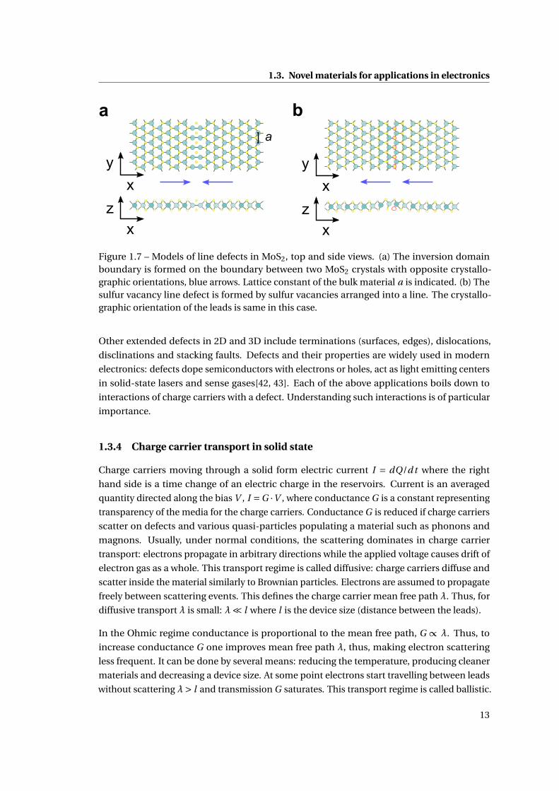
such defect is presented in Fig. 1.7(a). Since crystallographic orientations are bulk properties,
this defect cannot be removed without destroying one of the bulk domains completely. In
contrast, the sulfur vacancy line can be avoided by adding missing sulfurs locally, Fig. 1.7(b).
There, bulk crystal orientations coincide.
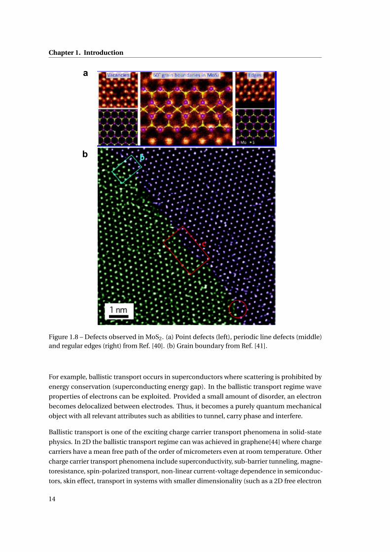
In experiments, the defects in 2D are identified using microscopy techniques such as scan-
ning tunneling microscopy (STM), transmission electron microscopy (TEM), atomic force
microscopy (AFM). An example of resulting images is given in Fig. 1.8 where different kinds of
defects (point and line) in a monolayer MoS2 are presented.
12
1.3. Novel materials for applications in electronics
Figure 1.7 – Models of line defects in MoS2, top and side views. (a) The inversion domainboundary is formed on the boundary between two MoS2 crystals with opposite crystallo-graphic orientations, blue arrows. Lattice constant of the bulk material a is indicated. (b) Thesulfur vacancy line defect is formed by sulfur vacancies arranged into a line. The crystallo-graphic orientation of the leads is same in this case.
Other extended defects in 2D and 3D include terminations (surfaces, edges), dislocations,
disclinations and stacking faults. Defects and their properties are widely used in modern
electronics: defects dope semiconductors with electrons or holes, act as light emitting centers
in solid-state lasers and sense gases[42, 43]. Each of the above applications boils down to
interactions of charge carriers with a defect. Understanding such interactions is of particular
importance.
1.3.4 Charge carrier transport in solid state
Charge carriers moving through a solid form electric current I = dQ/d t where the right
hand side is a time change of an electric charge in the reservoirs. Current is an averaged
quantity directed along the bias V , I =G ·V , where conductance G is a constant representing
transparency of the media for the charge carriers. Conductance G is reduced if charge carriers
scatter on defects and various quasi-particles populating a material such as phonons and
magnons. Usually, under normal conditions, the scattering dominates in charge carrier
transport: electrons propagate in arbitrary directions while the applied voltage causes drift of
electron gas as a whole. This transport regime is called diffusive: charge carriers diffuse and
scatter inside the material similarly to Brownian particles. Electrons are assumed to propagate
freely between scattering events. This defines the charge carrier mean free path λ. Thus, for
diffusive transport λ is small: λ¿ l where l is the device size (distance between the leads).
In the Ohmic regime conductance is proportional to the mean free path, G ∝ λ. Thus, to
increase conductance G one improves mean free path λ, thus, making electron scattering
less frequent. It can be done by several means: reducing the temperature, producing cleaner
materials and decreasing a device size. At some point electrons start travelling between leads
without scattering λ> l and transmission G saturates. This transport regime is called ballistic.
13
Chapter 1. Introduction
Figure 1.8 – Defects observed in MoS2. (a) Point defects (left), periodic line defects (middle)and regular edges (right) from Ref. [40]. (b) Grain boundary from Ref. [41].
For example, ballistic transport occurs in superconductors where scattering is prohibited by
energy conservation (superconducting energy gap). In the ballistic transport regime wave
properties of electrons can be exploited. Provided a small amount of disorder, an electron
becomes delocalized between electrodes. Thus, it becomes a purely quantum mechanical
object with all relevant attributes such as abilities to tunnel, carry phase and interfere.
Ballistic transport is one of the exciting charge carrier transport phenomena in solid-state
physics. In 2D the ballistic transport regime can was achieved in graphene[44] where charge
carriers have a mean free path of the order of micrometers even at room temperature. Other
charge carrier transport phenomena include superconductivity, sub-barrier tunneling, magne-
toresistance, spin-polarized transport, non-linear current-voltage dependence in semiconduc-
tors, skin effect, transport in systems with smaller dimensionality (such as a 2D free electron
14

1.3. Novel materials for applications in electronics
gas or a 1D nanowire transport), transport through quantum dots, Coulomb blockade, Kondo
effects and many more. Most of these phenomena are already implemented in real devices
making the study of electron transport one of the most important topics in the solid-state
physics and materials science.
15


2 Methodology
2.1 Density functional theory (DFT)
Density functional theory (DFT) is a tool to describe and calculate electronic, mechanical and
optical properties of materials and molecules. It is usually referred to as ab-initio (Latin “from
the beginning”) to make contrast with empirical approaches relying on experimental data1.
DFT starts from properties of individual elementary particles (electrons, protons) to form a
complete description of a material. This section is dedicated to key points about DFT and the
role of charge density in description of materials’ electronic properties.
2.1.1 Kohn-Sham equations
Electronic properties include different aspects of behavior of electrons: motion, interaction,
correlations. In solid state, electrons are found only in the vicinity of positively charged
atomic nuclei of the solid forming a Coulomb potential well. The mass of a single atomic
nucleus is 3-4 magnitudes larger than the mass of an electron. Thus, any kind of excitation
will cause electrons to reach equilibrium much faster than heavy atomic nuclei. This means
that above certain time scale (femtoseconds), electrons are in equilibrium with an underlying
atomic structure which may be considered to be “pinned” to the surrounding space. Thus,
the atomic nuclei can be simplified to classical point objects with mass and charge, the Born-
Oppenheimer approximation. The quantum mechanical nature of the atomic nucleus is
completely neglected. This allows to write the following electronic Hamiltonian:
H = T +V +U =N∑i
(− ħ2
2mi∇2
i
)+
N∑i
V (~ri )+N∑
i< jU (~ri ,~r j ) , (2.1)
where T is the kinetic energy of electrons, V is the external potential created by nuclei and
U is the interaction between electrons. Above equation works well in solid state but still too
difficult to solve unless a very special case occurs (such as U = 0). The reason for that lies in
1Modern DFT, however, often includes empricial constants in approximate exchange-correlation functionals
17
Chapter 2. Methodology
the quantum mechanical nature of electrons: each of them exists in a dedicated space such
that for N electrons one has a 3N -dimensional wavefunction to be found: ψ(r1,r2, ...,rN). The
complexity to solve Eq. 2.1 grows exponentially with the number of electrons and is commonly
believed to be too high. A rather obvious simplification here is to limit consideration from
3N -dimensional space to 3D with a single-particle picture of electron interactions. Two of
the three terms in Eq. 2.1 are single-particle terms: both kinetic energy and external potential
are defined for a single electron. In contrast, the third term U representing electron-electron
interaction is meaningless for a single electron. The mean-field approximation overcomes
this issue.
The mean-field approximation takes different forms in different solid-state problems but the
idea is always the same: replace the two-particle potential by interaction of a particle with a
particle density. The mean field captures all classical aspects of interaction and is a starting
point for more advanced methods (such as the configuration interaction approach). Under
the mean-field approach, the Coulomb interaction U in Eq. 2.1 becomes an interaction with a
charge density, a spin exchange interaction becomes an interaction with magnetic moments
and so on. The mean-field approximation is usually designed in a way to be able to reproduce
exact interaction in non-correlated systems which can be solved exactly.
In DFT, the mean field is presented by the exchange-correlation functional replacing the
electron-electron interaction term and depending on the charge density ρ(r) in the most
general way[45]. The Hamiltonian becomes a functional of the charge density ρ(r):
HKS(ρ(r))ψi =(− ħ2
2m∇2 +V (r)+µxc
[ρ (r)
])= Eiψi , (2.2)
where µxc is the exchange-correlation functional of the charge density ρ. This Hamiltonian is
a Kohn-Sham Hamitlonian introduced in 1965[46]. It is complemented by the corresponding
charge density in the real space
ρ(r) =∑i
f (Ei )∣∣ψi (r)
∣∣2 (2.3)
where f (E) is the Fermi-Dirac energy distribution function. Above two equations are Kohn-
Sham equations to be solved self-consistently. Resulting solution minimizes the Kohn-Sham
total energy functional Etot(ρ) and is an exact ground state charge density with an exact total
energy Etot according to Hohenberg-Kohn theorems.
2.1.2 Limitations of DFT
So does DFT solve the many-body problem in general? The answer is “no” because the exact
exchange-correlation functional and, thus, the Hamiltonian are unknown2. However, there
2Knowing exact exchange-correlation functional makes no sense anyway: computing it will likely involve asmuch resources as the original problem Eq. 2.1 does.
18

2.1. Density functional theory (DFT)
are reasonable approximations to the contribution Exc of electron exchange and correlation
effects to the total energy called local density[46] and generalized gradient[47] approximations
(LDA and GGA):
E LDAxc =
∫εLDA(ρ(r))ρ(r) dr , (2.4)
E GGAxc =
∫εGGA(ρ(r),∇ρ(r))ρ(r) dr . (2.5)
The symbol ε(...) is a simple function, thus, both approximations are local. These approxima-
tions provide a reasonable description of an overwhelmingly large number of experimentally
available systems. Otherwise more advanced techniques can be used, such as hybrid func-
tional approaches, the GW approximation, DFT+U schemes, etc. Some of these techniques
include empirical terms to fit experimental data. Moreover, the sole fact of the choice between
approximations makes DFT empiric as reflected in several studies[48, 49].
Without knowing an exact exchange-correlation functional DFT is rather an empiric model
than a formally valid approximation: it is difficult to estimate and systematically reduce errors
of the total energy or any other quantity computed by DFT. In other words, it is impossible
to know how good LDA, GGA or any other approximation solves the electronic Hamiltonian
Eq. 2.1.
The Hohenberg-Kohn theorems stating existence of an exact total energy functional Etot(ρ(r))
are not practical either: they refer to the ground state only and do not guarantee existence of
expressions for other important quantities to compute (such as excited states of a solid, for
example). Thus, the single-particle states ψi in Eqs. 2.2,2.3 lack physical meaning, especially
for strongly-correlated systems.
Nevertheless, DFT describes well most nanoscale systems without strong correlations. This in-
cludes crystals and isolated systems, conductors and insulators, systems with magnetic order,
disordered systems including liquid, amourphous materials and alloys, materials with defects
and many more. The success of DFT may be attributed to the fact that it is relatively simple to
understand and undemanding; the solutions of Eq. 2.2 can be predicted and reproduced. This
makes DFT a leading computational tool and a gold standard in material science, solid-state
physics and chemistry fields.
2.1.3 DFT in crystals, the Bloch theorem and the Brillouin zone
Crystal is a solid material extending infinitely in one or more directions with atoms preserving
long-range translational order. Inside a crystal, a lattice can be defined where atoms occupy
well-defined positions, such as a hexagonal lattice in graphene, Fig, 1.4. Crystalline lattices
are periodic: the atoms occupying lattice cites can by exchanged by simply shifting the whole
19

Chapter 2. Methodology
lattice by some vector ~d . All such possible vectors are called translation vectors referring to
the translational symmetry of the lattice. Depending on whether a lattice is 1D, 2D or 3D
there exist D = 1,2 or 3 linearly independent lattice vectors ~ai forming a basis set for possible
translations:
~d = {ni } = ∑i=1..D
ni ~ai , (2.6)
where ni are integers. The vectors ~ai form a unit cell of the lattice while various sets of vectors~d form supercells. However, the choice of vectors ~ai and a unit cell is not unique. For example,
negative vectors −~ai also satisfy Eq. 2.6, thus, they form another unit cell having the same
volume.
A unit cell of a crystal contains a finite amount of atoms, for example, 2 carbon atoms in
graphene and a single molybdenum atom together with 2 sulfur atoms in MoS2. Thus, a
periodic crystal is described by a single unit cell with a few atoms inside it. For the quantum
mechanical treatment, it is possible to replace an infinite crystalline solid by a single unit cell
by using the Bloch theorem. It gives an integral of motion, the pseudomomentum k, for an
electronic wavefunction in a periodic environment. Mathematically, the Bloch theorem allows
to diagonalize an infinite matrix with a periodic structure. For example, consider following
tridiagonal matrix H which may be viewed as a single-band model Hamiltonian of an infinite
atomic chain where each atom with the energy ε interacts with nearest neighbors only through
the hopping integral λ:
H =
. . . . . . . . . . . . .
. . . ε λ 0 0 . . .
. . . λ∗ ε λ 0 . . .
. . . 0 λ∗ ε λ . . .
. . . 0 0 λ∗ ε . . .
. . . . . . . . . . . . .
. (2.7)
Hamiltonian H is Hermitian though it is not important for the Bloch theorem. The eigenvalue
equation Hψ= Eψ results in the following equation for the wavefunction element ψi
λψi−1 +εψi +λ∗ψi+1 = Eψi , (2.8)
where i is the index of an atom, an arbitrary integer. Generally, to solve the above system
of equations one needs to fix 2 arbitrary values of ψ (boundary conditions) as well as the
energy E . Or the other way, for each energy E the wavefunction ψ is a linear combination of
two orthogonal functions, i.e. all states are doubly degenerate. To find both states a Fourier
transform is performed such that
ψi+1 = cψi , (2.9)
20
2.1. Density functional theory (DFT)
yielding following quadratic equation
λc−1 +ε+λ∗c = E . (2.10)
The above quadratic equation has two solutions in general3. Thus the ansatz, Eq. 2.9 diagonal-
izes the Hamiltonian Eq. 2.7. The eigenstates are simply ψi = c iψ0, the fact known as Bloch
theorem for |c| = 1. In the latter case, a complex phase κ is gained for the wavefunction in
each cosequetive unit cell
ψn =ψ0e i nκ . (2.11)
Finally, if |c| 6= 1 the state ψ cannot be normalized: it grows to infinity in positive or negative
direction. Such states may exist in a finite system but they are usually irrelevant for bulk
crystals. By substituting Eq. 2.11 into Eq. 2.8 it is possible to derive the energy dispersion as a
function of κ
E(κ) = ε+2Reλ ·cosκ+2Imλ · sinκ . (2.12)
The quantity κ is a Bloch wave number, the integral of motion of Hamiltonian Eq. 2.7.
To complete the picture of the Bloch approach, consider a real space periodic Hamiltonian
originating from, for example, DFT description of a crystalline solid. There, the translational
invariance is expressed as H (~r ) = H (~r + ~d) where ~d is a lattice vector. The shifted wavefunction
gains phase
ψ(~r + ~d) =ψ(~r ) ·e i~k·~d . (2.13)
Re-writing above gives
ψ(~r2) =ψ(~r1) ·e i~k·(~r2−~r1) , (2.14)
where~r1,2 correspond to same point in different unit cells of the crystal. Finally, the Bloch
function φ is defined as
ψ(~r2)e−i~k·~r2 =ψ(~r1) ·e−i~k·~r1 =φ(~r2) =φ(~r1) . (2.15)
As it is evident, it is periodic in solid and differs from the wavefunction by a Bloch factor e i~k·~r
ψ(~r ) =φ(~r )e i~k·~r . (2.16)
The Bloch function is an eigenstate of the Bloch Hamiltonian defined as a Fourier transform
3Including infinitely large solutions. Cases with coinciding solutions (ε−E)2 = 4|λ|2 correspond to band edgesand are not considered.
21

Chapter 2. Methodology
Figure 2.1 – The periodic reciprocal space for a 2D hexagonal lattice such as graphene. Thereciprocal unit cell is highlighted in blue while the (first) Brillouin zone is a green hexagon.The high-symmetry points Γ, M, M1,2, K, K’ are indicated.
of the periodic Hamiltonian inside the unit cell (U.C.):
H(~k) =∫
U.C.
d~r e i~k·~r ·H(~r ) . (2.17)
Calculating the Hamiltonian in real ~r -space and transforming it into reciprocal ~k-space is
often a part of self-consistent procedure to solve DFT Eqs. 2.2,2.3.
Diagonalizing H(~k) yields energy eigenvalues En(~k) depending on the wave vector~k and the
band index n. En(~k) is usually referred to as electronic band structure, examples are given in
Fig. 1.3 (b,d). Since H(~k) is periodic in reciprocal space it is possible to define the reciprocal
unit cell. The (first) Brillouin zone is defined on the basis of the reciprocal unit cell, see Fig. 2.1
as an example. The Brillouin zone has its center~k = 0 and contains locus of points that are
closer to the origin than to any other periodic replica of Γ. Though both the reciprocal unit
cell and the Brillouin zone can be used to describe reciprocal space, the former one usually
contains more relevant symmetries such as the hexagonal symmetry in the example in Fig. 2.1.
The Bloch description is essentially a Fourier transform of the Hamiltonian given in Eq. 2.17.
It simplifies the eigenvalue equation, however, many more problems have to be solved during
the self-consistent cycle. One more example where the Fourier transform gives unbeatable
performance is the calculation of a Coulomb potential Vc (~r ) from periodic charge density ρ(~r ).
The Laplace equation connecting both has the following form
∆Vc (~r ) = ρ(~r ) , (2.18)
where ∆ is the Laplace second derivative operator. Depending on the boundary conditions,
different methods can be used to solve it. The simplest case, however, is when periodic
22

2.1. Density functional theory (DFT)
boundary conditions are assumed. In this case, it is possible to transform the above equation
into reciprocal space where it becomes a trivial expression
Vc (~k)
k2 = ρ(~k) . (2.19)
In 3D, the time needed to perform the Fourier transform scales with the number of grid points
along one of the dimensions N as N 3 log N which is much better than if boundary conditions
would have been located at infinity with time scaling of N 6. Thus, even isolated systems
without PBC are usually considered to be periodic within large enough unit cell to avoid
interaction between replicas.
2.1.4 Core electrons and pseudopotentials
As it was described in the previous section, a typical subject of the DFT is a periodic unit of a
solid – the unit cell containing several atoms. The number of electrons in a unit cell is a sum
of atomic numbers of all unit cell atoms Zi . Sometimes this number is small (there are 24
electrons per unit cell of graphene for example), but may also grow to thousands if a more
complex problem is considered. A further simplification was developed to reduce the number
of electrons considered called the pseudopotential approximation.
To understand the pseudopotential approximation, consider an atomic nucleus with Z protons
creating a Coulomb potential V (~r ) = −Z /|r |. It is known since Niels Bohr (1913) that such
potential hosts discrete electronic orbitals with energies varying from tens to fractions of eV.
Electrons with smaller energies form the valence shell of an atom while the rest of electrons
are localized around the nucleus (core electrons). The size of the corresponding orbitals is
much smaller than the interatomic distance, thus, the core electrons do not participate in
most properties such as chemical bonding, low-energy excitations and transport. The idea
behind pseudopotential approximation is to remove core electrons from the consideration by
replacing Coulomb potential with a pseudopotential.
To construct a pseudopotential one performs the following steps:
1. Choose an atom and perform an all-electron calculation of electronic states ψaei and
corresponding energies Ei within selected DFT formalism;
2. Choose an energy threshold Ethreshold and assign all states below this energy Ei <Ethreshold to be core states:
• smaller Ethreshold includes more electrons in the valence, thus, the pseudopotential
becomes more exact and more computationally expensive;
• larger Ethreshold includes more electrons in the core instead: these electrons be-
come “frozen” and the pseudopotential becomes less transferrable but also com-
putationally cheaper;
23

Chapter 2. Methodology
3. Pick a core radius rc above which the valence electronic wavefunction of the future
pseudopotential ψpsi matches exactly the corresponding all-electron wavefunction
ψaei (r ) =ψps
i (r )|r>rc . This parameter discards properties of the valence wavefunctions
inside the core similarly to the core states being discarded. Thus:
• the core radius rc should be smaller than, literally, half of the bond length between
atoms in a solid;
• but it should be larger4 than the distance to the outermost radial node of ψaei ;
• larger rc gives more freedom to construct a “softer” pseudopotential with smoother
wavefunctions and better convergence properties;
• in contrast, smaller rc in hard pseudopotentials will reproduce bonding better for
the cost of performance. Resulting pseudopotential becomes more universal and
transferable between different solids;
• rc may be chosen individually for each state ψpsi ;
4. Construct pseudowavefunctions ψpsi inside the core matching various conditions such
as softness, conservation of norm and matching of logarithmic derivatives. This step
ensures various physical quantities such as lattice constant, binding energy, etc are
reproduced correctly.
5. Restore the pseudopotential by calculating Vps = ∑i|ψps
i ⟩Ei ⟨ψpsi | −T , where T is the
kinetic energy operator. For Vps to be local one has to take necessary measures at the
previous step.
6. For convenience, one also has to remove Hartree and exchange-correlation contribu-
tions which will be taken into account when this pseudopotential is used in a calculation
of a solid.
As it was pointed out, the pseudopotential has to be transferable: it should reproduce as many
experimentally available quantities as possible. Constructing such pseudopotential, however,
is a trial and error process.
2.1.5 Electron spin and spin-orbit coupling in DFT
The physics of an electron spin σ=↑,↓ in DFT may be presented by spin-dependent charge
density ρσ(~r ) and wavefunctions ψσ(~r ). In the simplest case of a scalar-relativistic approxi-
mation, the whole Kohn-Sham Hamiltonian is split into two spin-dependent parts Hσ solved
separately. In spin-neutral systems the Hamiltonians become equal: H↑ = H↓. In this case,
every electronic state is at least doubly degenerate and hosts pairs of electrons with opposite
spins. Upon adding magnetic field or spontaneous spin polarization the energy levels become
4To make the pseudopotential local the nodes ψ(r )ae = 0 cannot be reproduced by the pseudowavefunctionψ
psi , see Fig. 2.2
24

2.1. Density functional theory (DFT)
Figure 2.2 – A sketch of a pseudopotential Vps and the corresponding wavefunction ψps versusCoulomb potential of the atomic nucleus and the all-electron wavefunction ψae (dashes).
split: one of the spin occupies a more energetically favorable configuration while the other
one stays at higher energies, the effect named after Dutch physicist P. Zeeman. Corresponding
energy gain is
∆=−~µB ·~B , (2.20)
where ~B is a vector of magnetic field or an exchange field and µB is Bohr’s magneton: electron
magnetic moment. According to the above formula, the vector field causes a non-zero spin
polarization.
The Zeeman term, however, is the consequence of a more general relativistic Dirac Hamil-
tonian for an electron traveling at relativistic speeds. It was proposed in 1928 and has the
following form
iħdψ
d t= (
c~α ·~p +βme c2)ψ , (2.21)
where ħ is the Planck’s constant, ψ is a four-component wavefunction, c is the speed of light,
~p is a momentum of an electron, me is electron mass and α, β are 4x4 matrices
αx,y,z =[
0 σx,y,z
σx,y,z 0
], β=
1 0 0 0
0 1 0 0
0 0 −1 0
0 0 0 −1
, (2.22)
σi are Pauli spin operators
σx =[
0 1
1 0
], σy =
[0 −i
i 0
], σz =
[1 0
0 −1
]. (2.23)
25

Chapter 2. Methodology
The external electromagnetic field is introduced via a scalar potential φ and a vector potential~A interacting with electron charge q
iħdψ
d t= (
c~α · [~p −q~A]+βme c2 +qφ)ψ . (2.24)
To identify the most important terms, the wavefunction is split into a couple of two-component
spinors ψ1, ψ2 (electron and positron wavefunctions). It becomes possible to write down the
following system
iħdψ1
d t = c~σ · [~p −q~A]ψ2 +(me c2 +qφ
)ψ1
iħdψ2
d t = c~σ · [~p −q~A]ψ1 +(−me c2 +qφ
)ψ2 .
(2.25)
Its time-independent form is
0 = c~σ · [~p −q~A]ψ2 +(−E +qφ
)ψ1
0 = c~σ · [~p −q~A]ψ1 +(−E −2me c2 +qφ
)ψ2 .
(2.26)
Note that me c2 is a constant energy shift. Taking me c2 to be the largest energy scale in the
problem, it is possible to expand the above two equations in powers of 1/c. The solution of
the system up to the second order is the following
[(~p −q~A)2
2me+qφ− ħq
2me~σ ·~B − p4
8m3e c2
+ ħ2q
8m2e c2
∆− ħq
4m2c2~σ · [(~p −q~A)×∇]]
ψ1 = Eψ1 ,
(2.27)
where ~B = ∇× ~A - magnetic field, ∆ - Laplace operator. The first three terms in the above
constitute a non-relativistic Hamiltonian of an electron in electric and magnetic fields. In
particular, the third term is the Zeeman term introduced in the beginning of the section. The
rest of the terms are known as relativistic corrections to the energy: mass, Darwin and spin-
orbit couplings (the last term). The spin-orbit term, in particular, couples electron spin and
momentum. It is non-local and, thus, cannot be reduced to magnetic field action. The wave-
functionψ=ψ1 is the spinor wavefunction containing superposition of the electronic spin-up
and spin-down states. Thus, the general form of the Kohn-Sham spin-orbit Hamiltonian is
non-local in spin Hσ,σ′ 6= 0. Similarly, the charge density matrix ρσ,σ′ has spins coupled.
Relativistic treatment is especially important for solids with heavy atoms where electron
momentum p is large. There, the spin-orbit coupling causes energy splittings in the band
structure and spin polarization of bands like in the case of MoS2 illustrated in Fig. 1.3(d).
2.1.6 Single-electron basis in DFT
To be able to solve Kohn-Sham equations numerically one has two write every relevant quan-
tum mechanical operator in some basis set. The most popular basis sets used in existing
26

2.1. Density functional theory (DFT)
Plane waves Localized basis sets Mixed basis sets
Origin eigenstates of the mo-mentum operator p
atomic or atomic-like(gaussian) wavefunc-tions
both types of statesform the basis
In r -space e i k0r localized bothIn k-space δ(k −k0) quasi-delocalized both
Parameters cutoff kmax specifyingnumber of planewaves
various parameters de-scribing the numberand shapes of wave-functions
both
Completeness when kmax →∞ non-systematic as in plane wavesOrthogonality 3 7 7
Pros Easy to introduce; sys-tematic convergencewith respect to kmax;describes well valenceand free electrons; nooverhead with respectto the Fourier trans-form
Compact flexible basissets for both smalland large systems;work well for isolatedmolecules; natu-ral basis for orbitalanalysis and all-electron calculations;computationallyundemanding
Combines the ad-vantages of both; de-signed for descriptionof complex systemssuch as a molecule ona metallic surface
Cons Impossible to usewithout pseudopoten-tial approximation;isolated, truncatedsystems such as sur-faces and moleculesrequire significantlylarger basis sets
No systematic con-vergence; free-likeelectrons requireadditional basis func-tions; the number ofparameters to tweak isroughly equal to thenumber of electronsin the system; numer-ical problems relatedto non-orthogonality
The steepest learningcurve; numericalproblems related tonon-orthogonality;efficient implemen-tation requires enor-mous effort; introduc-tion of new featuresis delayed because ofthe above
Table 2.1 – Comparison of basis sets used in DFT simulations.
DFT simulation programs in materials science are either plane waves, localized basis sets or a
mixture of both. Table 2.1 contains a short summary on the three options.
27

Chapter 2. Methodology
Figure 2.3 – A schematic illustration of a two-terminal ballistic transport setup. The sulfurvacancy line defect in MoS2 plays a role of a potential barrier for ballistic charge carriers. Theincoming mode from one of the leads is split into reflected mode as well as the transmittedmode traveling to another lead.
2.2 Ballistic transport at nanoscale with DFT
While DFT is a study about ground state properties, experimental spectroscopic studies probe
materials by driving them into an excited state and reading out the response. A number of
extensions to DFT have been developed to simulate different kinds of a non-equilibrium state
which also includes particle transport phenomena. As it was already pointed out previously,
DFT does not guarantee correctness of any other quantity except total energy and charge
density unless exchange and correlation effects can be neglected. It is the case in the ballistic
transport regime where two-particle scattering effects are rare. While the concept of ballistic
transport was introduced previously in this section practical some aspects are covered.
The ballistic transport regime is defined as a regime where the distance between charge carrier
reservoirs (contacts, leads) is smaller than the mean free path (the mean distance between
charge carrier two-particle scattering events). The leads host electronic states which are the
endpoints for electronic transport. The states in the leads are referred to as lead modes in
Fig. 2.3. Ballistic charge carriers are transmitted between lead modes via channels in the
scattering region. The channels define the charge carrier current resistance R which can be
measured. Once a voltage is applied the charge carriers will start moving towards negative bias
and will soon reach a dynamical equilibrium resulting in a stationary regime for the charge
density in the scattering region.
Depending on resistance R, some charge carriers will reflect from the scattering region back
to the origin lead. The rest of the charge carriers will transmit further. The probability of being
transmitted through the scattering region is called transmission probability T . Transmission
probability is a function of various parameters such as energy of the charge carrier, shape of
the lead modes and electrostatic potential in the scattering region. Transmission probability
28

2.2. Ballistic transport at nanoscale with DFT
has no units and takes values from 0 (no transmission, all charge carriers reflected) to 1 (all
charge carriers transmitted). Based on values of T , the scattering region is characterized to
be reflective or transparent by analogy with reflection of light. The resistance R is inversely
proportional to the sum of transmission probabilities of all channels Ti
R = h
e2 ∑i
Ti. (2.28)
The quantity 2e2
h combining electron charge e and Planck’s constant h is called conductance
quantum: a maximum possible conductance achieved by a single charge carrier transmis-
sion channel. The resulting charge carrier current is computed using the Landauer-Buttiker
formula
I = e
h
∫dET (E) f ′(E) , (2.29)
where f ′(E) is the perturbation to the equilibrium distribution function and T is the sum of
transmission probabilities at a given energy.
The total energy E of a ballistic charge carrier is conserved if no inelastic processes are present.
For 2D (atomic layers) and 3D (bulk) leads we will also consider conservation of the pseudo-
momentum~k|| orthogonal to the transport direction provided the entire system is a subject to
periodic boundary conditions. For example, the pseudomomentum along the periodic line
defect shown in Fig. 2.3 is conserved. After integrating out all conserved quantities the scatter-
ing problem becomes a 1D quantum mechanical problem for a particle traveling through the
barrier. It can be solved efficiently using the Green’s function formalism.
2.2.1 Green’s function formalism
The Green’s function formalism is widely adopted for calculation of ballistic transport proper-
ties, see Refs. [50, 51, 52] for examples. It allows to take into account semi-infinite leads in an
exact way via their surface Green’s functions and self-energies. This method is general enough:
it does not make any assumptions of the underlying structural and electronic properties such
as the presence of band gap, magnetic ordering, dimensions of the setup or number of leads.
There are several pre-requisites that have to be satisfied, though:
1. The leads are assumed to be ideal: all defects are present in the scattering region only.
2. The setup should be effectively one-dimensional. The treatment of 2D and 3D systems
is also possible by introducing conserved projections of the pseudomomentum.
3. The Hamiltonian should be written in a tri-block-diagonal form. Practically, this means
that the basis set for the Hamiltonian is localized and Hamiltonian matrix elements are
truncated at a finite distance.
29

Chapter 2. Methodology
Figure 2.4 – Ideal and defective 2D systems. (a) A pristine graphene monolayer possessinga periodic atomic structure. The nearest neighbor tight-binding Hamiltonian of graphenewithout spin-orbit coupling λSO = 0 from Ref. [23] consists of 5 Hamiltonian matrices hi
expressed in a localized atomic-like basis set (p orbitals of carbon). Corresponding hoppingvectors ~Ri in Eq. 2.30 are expressed in terms of lattice vectors: ~R0 = 0, ~R1 =~a2, ~R2 =~a1, ~R3 =−~a2, ~R4 =−~a1. (b) A line defect in monolayer MoS2. The setup with a regular line defect isperiodic only along its line. To describe a periodic line defect in MoS2 one should considerconservation of pseudomomentum along the defect line k||.
Procedure described further follows the mode matching approach from Ref. [53] while certain
aspects of it have been simplified, improved and generalized by the author of this thesis. The
recipe is outlined below.
Step 0: Integrate out projected pseudomomentum k||
Before proceeding to the Green’s function approach to electron transport dimensions of the
system have to be reduced. This is done by integrating out projection of the pseudomomentum
k|| commuting with the initial Hamiltonian.
The Bloch form of a bulk periodic Hamiltonian expressed in a localized basis set is a finite sum
of blocks with Bloch pre-factors
H(~k) =∑i
hi e i~k~Ri , (2.30)
where hi are finite-sized Hamiltonian matrices describing interactions between the unit cell
at the origin and its displaced replica translated by the vector ~Ri
Ri = ni~a1 +mi~a2 +ki~a3 = (n,m,k)i , (2.31)
where ~ai are unit cell vectors, see also Fig. 2.4(a).
In the bulk geometry, Fig. 2.4(a), the pseudomomentum ~k is a conserved quantity. In the
device (defect) geometry, Fig. 2.4(b), one of the translation symmetries is no longer present.
30

2.2. Ballistic transport at nanoscale with DFT
It is still possible to apply the Fourier transform expressed in Eq. 2.30 to other dimension(s).
The pseudomomentum ~k becomes projection of the pseudomomentum onto the defect~k|| = (k2,k3), Fig. 2.4(b). In this way a 2D or a 3D problem is reduced to a 1D problem H(k||).
The latter can be viewed as nanowire with a point defect where~k|| is an external parameter.
Further in this section dependence on~k|| is omitted.
Step 1: Prepare the 1D device problem
Notation
• i index of the lead
• j index of the unit cell inside the lead; 0 stands for the unit cell in close proximity
to the device region; runs to +∞• r index of the lead mode (eigenstate)
• E energy of the charge carrier
• H infinite Hamiltonian matrix
• hd finite diagonal part of H corresponding to the device (scattering region)
• hi finite diagonal part of H corresponding to the lead i
• S infinite right-hand-side overlap matrix of the generalized eigenvalue equation
(GEE) for the Hamiltonian written in a non-orthogonal basis set Hψ= ESψ
• ψ arbitrary (right) solution of the GEE at energy E
• ψ arbitrary left solution of the GEE at energy E
• ψd part of ψ in the device region
• ψi , j part of ψ in the unit cell j of lead i
• φ(i ,r ), j r -th mode of the lead i in the unit cell j
• c(i ,r ) Bloch factor of the eigenmode r in the lead i
• W matrix present in the single-side form of GEE Wψ= 0: W = H−ES
• wd finite diagonal part of W corresponding to the device
• wi finite diagonal part of W corresponding to the unit cell of the lead i
• ai finite upper-diagonal part of W corresponding to interactions between
neighboring unit cells of the lead i
• bi finite lower-diagonal part of W corresponding to interactions between neigh-
boring unit cells of the lead i
• ai d finite upper-diagonal part of W corresponding to interactions between the
device and the closest unit cell j = 0 of the lead i
31

Chapter 2. Methodology
Figure 2.5 – Structure of a nanowire device Hamiltonian. (a) Schematic picture of the transportdevice setup. Several semi-infinite nanowires (leads) are connected to the same device. (b)A semi-infinite tri-block-diagonal Hamiltonian matrix of the setup is presented in panel (b)with a close-up of the device region in panel (c). The color of Hamiltonian blocks correspondsto leads’ and device color on panel (a). The white color represents zeros in the Hamiltonianmatrix.
• bi d finite lower-diagonal part of W corresponding to interactions between the
device and the closest unit cell j = 0 of the lead i
• F±i Bloch matrices for positive and negative modes in the lead i
Consider a ballistic setup where a nanoscale device connected to several semi-inifite periodic
leads, Fig. 2.5(a). It is possible to express this setup in a semi-infinite Hamiltonian, Fig. 2.5(b)
where ballistic charge carriers are the eigenstates of this Hamiltonian delocalized over multiple
leads. Thus, the eigenstates of such Hamiltonian provide transport channels for the charge
carriers.
As outlined previously, the Hamiltonian is expected to be in a tri-block-diagonal form where
the main diagonal in Fig. 2.5(c) corresponds to interactions within unit cell of the leads hi , i is
the lead index, and within the device region hd . The off-diagonal blocks couple leads and the
32

2.2. Ballistic transport at nanoscale with DFT
device region in the nearest-neighbor manner including “forward” coupling terms between
neighboring leads ai and coupling of the closest lead unit cell to the device ai d . Similarly, the
backward coupling terms bi , bi d are defined. Since Hamiltonian is Hermitian, h = h†, a† = b.
The nanowire device problem is the eigenvalue equation Hψ= Eψ. An alternative way to write
it is the following
(H−E)ψ= (H−E ·1)ψ= W(E)ψ= 0 . (2.32)
The matrix W(E) is tri-block-diagonal as well:
Wψ=
... ... ... ... ... ... ... ... ... ... ...
... wi ai
... w2 a2
... w1 a1
... bi wi ai
... b2 w2 a2
... b1 w1 a1
... bi wi ai d
... b2 w2 a2d
... b1 w1 a1d
... bi d b2d b1d wd
·
...
ψi ,2
ψ2,2
ψ1,2
ψi ,1
ψ2,1
ψ1,1
ψi ,0
ψ2,0
ψ1,0
ψd
= 0 , (2.33)
where w = h−E . The formal symbolic expression of the above equation consists of three types
of equations:∑i
bi dψi ,0 =−wdψd , (2.34)
biψi ,1 +ai dψd =−wiψi ,0 (2.35)
and
biψi , j+1 +aiψi , j−1 =−wiψi , j , j > 0 . (2.36)
The last type of equations correspond to bulk modes of lead i and are of the same form as
Eq. 2.8. It is easy to show5 that above equations need∑i
Ni boundary conditions, Ni being
number of rows (columns) in hi . In the transport problems the boundary conditions are
amplitudes of the leads’ modes. Thus the next step is to consider leads separately.
5For example, specify all ψi ,0
33
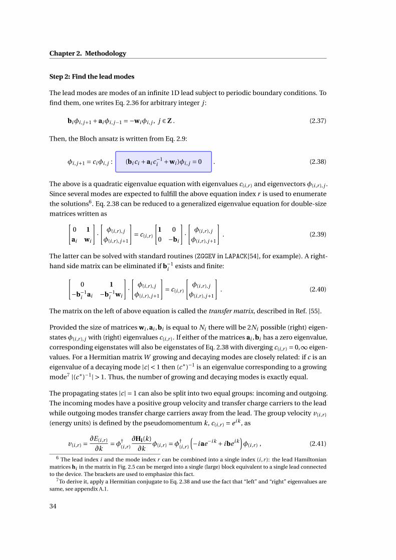
Chapter 2. Methodology
Step 2: Find the lead modes
The lead modes are modes of an infinite 1D lead subject to periodic boundary conditions. To
find them, one writes Eq. 2.36 for arbitrary integer j :
biφi , j+1 +aiφi , j−1 =−wiφi , j , j ∈ Z . (2.37)
Then, the Bloch ansatz is written from Eq. 2.9:
φi , j+1 = ciφi , j : (bi ci +ai c−1i +wi )φi , j = 0 . (2.38)
The above is a quadratic eigenvalue equation with eigenvalues c(i ,r ) and eigenvectors φ(i ,r ), j .
Since several modes are expected to fulfill the above equation index r is used to enumerate
the solutions6. Eq. 2.38 can be reduced to a generalized eigenvalue equation for double-size
matrices written as[0 1
ai wi
]·[φ(i ,r ), j
φ(i ,r ), j+1
]= c(i ,r )
[1 0
0 −bi
]·[φ(i ,r ), j
φ(i ,r ), j+1
]. (2.39)
The latter can be solved with standard routines (ZGGEV in LAPACK[54], for example). A right-
hand side matrix can be eliminated if b−1i exists and finite:[
0 1
−b−1i ai −b−1
i wi
]·[φ(i ,r ), j
φ(i ,r ), j+1
]= c(i ,r )
[φ(i ,r ), j
φ(i ,r ), j+1
]. (2.40)
The matrix on the left of above equation is called the transfer matrix, described in Ref. [55].
Provided the size of matrices wi ,ai ,bi is equal to Ni there will be 2Ni possible (right) eigen-
states φ(i ,r ), j with (right) eigenvalues c(i ,r ). If either of the matrices ai ,bi has a zero eigenvalue,
corresponding eigenstates will also be eigenstates of Eq. 2.38 with diverging c(i ,r ) = 0,∞ eigen-
values. For a Hermitian matrix W growing and decaying modes are closely related: if c is an
eigenvalue of a decaying mode |c| < 1 then (c∗)−1 is an eigenvalue corresponding to a growing
mode7 |(c∗)−1| > 1. Thus, the number of growing and decaying modes is exactly equal.
The propagating states |c| = 1 can also be split into two equal groups: incoming and outgoing.
The incoming modes have a positive group velocity and transfer charge carriers to the lead
while outgoing modes transfer charge carriers away from the lead. The group velocity v(i ,r )
(energy units) is defined by the pseudomomentum k, c(i ,r ) = e i k , as
v(i ,r ) =∂E(i ,r )
∂k=φ†
(i ,r )
∂Hi(k)
∂kφ(i ,r ) =φ†
(i ,r )
(−i ae−i k + i be i k
)φ(i ,r ) , (2.41)
6 The lead index i and the mode index r can be combined into a single index (i ,r ): the lead Hamiltonianmatrices hi in the matrix in Fig. 2.5 can be merged into a single (large) block equivalent to a single lead connectedto the device. The brackets are used to emphasize this fact.
7To derive it, apply a Hermitian conjugate to Eq. 2.38 and use the fact that “left” and “right” eigenvalues aresame, see appendix A.1.
34

2.2. Ballistic transport at nanoscale with DFT
or,
v(i ,r ) = iφ†(i ,r )
(bc(i ,r ) −ac∗(i ,r )
)φ(i ,r ) . (2.42)
The number of incoming modes vi < 0 is equal to the number of outgoing modes vi > 0.
The group velocity calculated using Eq. 2.42 for non-propagating modes is zero. To show it
consider φn , cn and φm and cm is an arbitrary pair of solutions of Eq. 2.38 (the lead index i
and the unit cell index j are omitted):{(bcn +ac−1
n +w)φn = 0
(bcm +ac−1m +w)φm = 0 .
(2.43)
Multiplying the first equation to the left by φ†m and the second one by φ†
n yields{φ†
m(bcn +ac−1n +w)φn = 0
φ†n(bcm +ac−1
m +w)φm = 0 .(2.44)
Provided H is Hermitian, the conjugate operation applied to the second equation results in
φ†m(bc−1∗
m +ac∗m +w)φn = 0 . (2.45)
Subtracting the first equation in the system from the above eliminates w
φ†mbφn
(c−1∗
m − cn)+φ†
maφn(c∗m − c−1
n
)= 0 . (2.46)
Finally, multiplying the above equation by cnc∗m yields
φ†mbφn · cn
(1− cnc∗m
)+φ†maφn · c∗m
(c∗mcn −1
)= 0 ⇔[φ†
mbφn · cn −φ†maφn · c∗m
]· (1− cnc∗m
)= 0 .(2.47)
For n = m the quantity in square brackets is the group velocity up to i multiplier
v(i ,r )(1−|c(i ,r )|2) = 0 . (2.48)
Thus, all modes having |c| 6= 1 do not transmit charge carriers since the corresponding group
velocity v(i ,r ) = 0. A generalized velocity vnm will be used further. It is defined as
vnm = iφ†m
(b · cn −a · c∗m
)φn . (2.49)
vnm has a property
vnm(1− cnc∗m) = 0 , (2.50)
where both n and m identify modes, i.e. contain lead i and mode r indices.
35
Chapter 2. Methodology
Figure 2.6 – Boundary conditions and unknown amplitudes in the transport setup. Eachsquare represents an amplitude of the mode r in the lead i Ar
i . The entire row representsa wavefunction in one of the leads: it consists of incoming modes (green), outgoing modes(blue) and growing/decaying modes (red). The total number of amplitudes needed to describethe wavefunction in the lead i is equal to 2Ni . In the transport setup half of all amplitudes arefixed (left-hand side) while the other half is calculated. The source of electrons is representedby a sole incoming mode represented by the unity amplitude indicated by the arrow.
To sum up, a generic wavefunction of the lead i in the unit cell j , ψi , j , is expressed as a sum of
2Ni eigenmodes with complex amplitudes A(i ,r )
ψi , j =2Ni∑r=1
A(i ,r ) ·(c(i ,r )
) j ·φ(i ,r ),0 =∑
growing,|c|>1+ ∑
decaying,|c|<1+ ∑
incoming,v>0+ ∑
outgoing,v<0. (2.51)
In the transport setup some of the A(i ,r ) are boundary conditions, while, the other ones are
unknown. Specifically, all growing modes are discarded A(i ,r )> = 0: they diverge in the leads,
thus, lack physical meaning. To be able to calculate transmission probabilities, one assumes
that there is a single positive mode (i ,r )+s from the source lead with a unity amplitude
A(i ,r )+s = 1. Otherwise all other positive modes are absent: A(i ,r )+ = 0, (i ,r )+ 6= (i ,r )+s . It is
easy to see that the number of amplitudes defined so far is exactly equal to required number of
boundary conditions∑i
Ni , see Fig. 2.6. Thus, it is possible to derive another half of amplitudes
for decaying A(i ,r )< and outgoing A(i ,r )− modes.
Since all amplitudes Ari are split into two equal groups, the boundary conditions and the
unknown amplitudes in Fig. 2.6, it is also possible to split the wavefunctionψi , j into two terms
ψi , j =ψ+i , j +ψ−
i , j , (2.52)
where each term groups half of the sum from Eq. 2.51
ψ+i , j =
∑growing,|c|>1
+ ∑incoming,v>0
=∑r
c j(i ,r )φ(i ,r ),0 =
(F+
i
) j ·ψ+i ,0 ,
36
2.2. Ballistic transport at nanoscale with DFT
ψ−i , j =
∑decaying,|c|<1
+ ∑outgoing,v<0
=∑r
c j(i ,r )φ(i ,r ),0 =
(F−
i
) j ·ψ−i ,0 .
The quantities F are the Bloch matrices having the same combined spectrum as the transfer
matrix in Eq. 2.40
F+i = ∑
r∈{>,+}φ(i ,r ), j · c(i ,r ) · φ†
(i ,r ), j , F−i = ∑
r∈{<,−}φ(i ,r ), j · c(i ,r ) · φ†
(i ,r ), j . (2.53)
The row vector φ†(i ,r ), j is reciprocal to lead modes φ†
(i ,r ), j ·φ(i ,r ′), j = δr,r ′ provided the states
selected form a complete basis (proof omitted). It is easy to show that the above definitions do
not depend on the chosen j . The powers of Bloch matrices are simply(F±
i
)p = ∑r∈{...}
φ(i ,r ), j · cp(i ,r ) · φ†
(i ,r ), j . (2.54)
The Bloch matrices satisfy the following matrix equation:
bi F±i +ai
(F±
i
)−1 +wi = 0 , (2.55)
A final note on the Bloch matrices is related to the velocity expression in Eq. 2.49 which can be
re-written as:
vnm = iφ†m
(bi F+
i − (F+
i
)† ai
)φn , n,m ∈ {+} , (2.56)
vnm = iφ†m
(bi F−
i − (F−
i
)† ai
)φn , n,m ∈ {−} . (2.57)
The expression includes self-energies of the lead i defined as
Σi = bi F−i . (2.58)
The quantity i(bi F−
i − (F−
i
)† ai
)= i
(Σi −Σ†
i
)is the gamma-function
Γi = i(Σi −Σ†
i
), vnm =φ†
mΓiφn . (2.59)
37

Chapter 2. Methodology
Step 3: Solve the nanowire device problem
The next step is to determine all ψ−i , j for given ψ+
i , j by solving the corresponding system of
linear equations. To demonstrate it, Eqs. 2.34,2.35 are written using Eqs. 2.52 for j = 0∑i
bi dψ−i ,0 +wdψd =−∑
ibi dψ
+i ,0 , (2.60)
(bi F−i +wi )ψ−
i ,0 +ai dψd =−(bi F+i +wi )ψ+
i ,0 = ai(F+
i
)−1ψ+
i ,0 , (2.61)
where the right-hand side of the second equation was simplified using Eq. 2.55. Explicitly,
bi F−
i +wi ai d
b2F−2 +w2 a2d
b1F−1 +w1 a1d
bi d b2d b1d wd
·
ψ−
i ,0
ψ−2,0
ψ−1,0
ψd
=
ai
(F+
i
)−1ψ+
i ,0
a2(F+
2
)−1ψ+
2,0
a1(F+
1
)−1ψ+
1,0
−∑i
bi dψ+i ,0
. (2.62)
The left-hand-side matrix is the inverse of the Green’s function G of the scattering region. It
includes lead self-energies Σi from Eq. 2.58. This result is the same as the one presented in
Ref. [53] Eq. 19, except the right-hand-side term Q0c0(+) with Q0 defined in Eq. 14 of the above
reference. There, the lead-device matrices ai d , bi d are implicitly assumed to be projected
versions of ai bi such that
ai d = ai ·pi , bi d = qi ·bi (2.63)
where pi , qi are rectangular projection matrices, pi = q†i . Such notation change substituted
into Eq. 2.61 yields
piψd = (F+
i
)−1ψ+
i ,0 +(F−
i
)−1ψ−
i ,0 =ψi ,−1 , (2.64)
where ψi ,−1 is the lead mode as if the lead is continued to j = −1. Collecting above two
substitutions into Eq. 2.60 or Eq. 2.34 and replacing ψi ,0 in favor of ψi ,−1 by means of Bloch
matrices Eq. 2.52 results in the following∑i
qi biψi ,0 = ... =∑i
qi bi
[F+
i ψ+i ,−1 −F−
i ψ+i ,−1 +F−
i piψd
]=−wdψd . (2.65)
In the above equation, ψ+i ,−1 play the role of boundary conditions, similarly to ψ+
i ,0 in Eq. 2.62,
while ψd is an unknown. By moving ψd to the left and using self-energies from Eq. 2.58 a
simpler form of Eq. 2.62 is recovered[wd +∑
iqiΣi pi
]ψd =∑
iqi bi
(F+
i −F−i
)ψ+
i ,−1 . (2.66)
38

2.2. Ballistic transport at nanoscale with DFT
Similarly to Eq. 2.62, the left-hand-side matrix is the inverse of the Green’s function matrix G
G =[
wd +∑i
qiΣi pi
]−1
=[
wd +∑i
bi d b−1i Σi a−1
i ai d
]−1
. (2.67)
Note that usually qi , pi are dropped from the above expression assuming the former ones are
simple matrices consisting of zeros and ones. This creates unnecessary confusion especially
when considering real implementations: it usually requires to “include” a unit cell of each lead
into the scattering region matrix wd and to use special indexing rules.
Step 4: Calculate transmission probabilities
To calculate transmission probabilities one takes a special form of the right-hand-side vector
in Eq. 2.62 or Eq. 2.66 in accordance with Fig. 2.6
ψ+i , j = 0, i 6= is ; ψ+
i , j =φ(i ,r+)s , j , i = is , (2.68)
where the incoming “+” mode rs of the lead is is taken as a source of electrons. The charge
carriers scatter into an outgoing drain mode (i ,r−)d of the lead id with an amplitude
A(i ,r+)s→(i ,r−)d = φ†(i ,r−)d , jψ
−id , j . (2.69)
For id 6= is , Eq. 2.64 yields pidψd = ψid ,−1 = ψ−id ,−1, thus, Eq. 2.66 results in the following
amplitude
A(i ,r+)s→(i ,r−)d = φ†(i ,r−)d ,−1
(pid Gqis
)bis
(F+
is−F−
is
)φ(i ,r+)s ,−1 . (2.70)
Note that j =−1 is taken: while the amplitude A generally depends on the unit cell j where
the above projection is performed, its magnitude is constant for the propagating modes. The
amplitude of reflected waves can be found in a similar fashion. Reflected modes belong to the
source electrode, thus Eq. 2.64 reads
pisψd =ψis ,−1 =ψ−is ,−1 +φ(i ,r+)s ,−1 . (2.71)
To derive the amplitude, the outgoing part of the wavefunction in the source ψis ,−1 should be
projected onto one of the outgoing states φ(i ,r−)s ,−1
A(i ,r+)s→(i ,r−)s = φ†(i ,r−)s ,−1
(pid Gqis
)bis
(F+
is−F−
is
)φ(i ,r+)s ,−1 − φ†
(i ,r−)s ,−1φ(i ,r+)s ,−1 (2.72)
39

Chapter 2. Methodology
Transmission and reflection probabilities are proportional to the absolute of the above ampli-
tude squared:
tn→m = vm
vn|An→m |2 . (2.73)
It is normalized by velocity and takes values from 0 to 1. The total transmission from the
source to the drain lead includes the sum over incoming and outgoing modes in these leads
Tis→id = ∑n ∈ {(i ,r+)s , |c| = 1}
m ∈ {(i ,r−)d , |c| = 1}
tn→m . (2.74)
The above formulas together with Eq. 2.28 are sufficient to calculate a two-terminal resistance.
It is instructive, however, to recover Caroli expression[56, 57] for the total transmission
Tis→id = Tr Γid pid GqisΓis pis G†qid . (2.75)
The above equation and Eq. 2.70 essentially use the same components: the Green’s function G
and the gamma-functions Γ in the form of velocities vn , see Eq. 2.59. The main issue, however,
is that Eq. 2.70 together with Eq. 2.73 give a non-zero transmission probability for growing or
decaying modes φ, φ. Writing transmission probability explicitly yields
tn→m = vm
vn· φ†
m
(pid Gqis
)bis
(F+
is−F−
is
)φn ·φ†
n
(bis
(F+
is−F−
is
))† (pid G†qis
)φm . (2.76)
Above expression is zero if m denotes a decaying mode since vm =φ†mΓidφm = 0 in this case,
see Eq. 2.50. It diverges, however, if φn is a growing mode: vn = 0. A workaround is to consider
a part of the above expression bis
(F+
is−F−
is
)φn
bis
(F+
is−F−
is
)φn =
(bis F+
is−Σis
)φn =
(bis F+
is+ iΓis −Σ†
is
)φn =
iΓisφn +(bis F+
is−Σ†
is
)φn = iΓisφn +
(bis F+
is−
(F−
is
)†ais
)φn .
(2.77)
The operator in brackets multiplied by an incoming mode is always zero(bis F+
is−
(F−
is
)†ais
)φn = 1
(bis F+
is−
(F−
is
)†ais
)φn =∑
j∈{−}φ j φ
†j
(bis F+
is−
(F−
is
)†ais
)φn = ∑
j∈{−}φ j
[φ†
j
(bis F+
is−
(F−
is
)†ais
)φn
]=∑
j∈{−}φ j
[φ†
j
(bis cn − c∗j ais
)φn
]= ∑
j∈{−}φ j vn j = 0
(2.78)
40

2.2. Ballistic transport at nanoscale with DFT
since n is an incoming mode while j denotes outgoing and decaying modes such that 1−cnc∗j 6=0 in Eq. 2.508. Proceeding with Eq. 2.76,
tn→m = vm
vn· φ†
m
(pid Gqis
)Γisφn ·φ†
nÆis
(pid G†qis
)φm . (2.79)
Using Eqs. 2.59,2.50 it is a rather simple task to prove that Γisφn = vnφn . Canceling velocities
vn yields
tn→m = vm · φ†m
(pid Gqis
)φn ·φ†
nÆis
(pid G†qis
)φm . (2.80)
Also, Γidφm = vmφm such that
tn→m = φ†m
(pid Gqis
)φn ·φ†
nÆis
(pid G†qis
)Γidφm . (2.81)
The above expression produces the same exact values for transmission probabilities between
propagating modes as Eq. 2.76. However, it has an advantage of all non-physcial transmission
probabilities between growing and decaying modes being zero:
Γφ= vφ= 0, |c| 6= 1 ⇔ v = 0 . (2.82)
The total transmission becomes
Tis→id = ∑n ∈ {(i ,r+)s , |c| = 1}
m ∈ {(i ,r−)d , |c| = 1}
tn→m = ∑n ∈ {(i ,r+)s}
m ∈ {(i ,r−)d }
tn→m =
∑m,n
φ†m
(pid Gqis
)φn ·φ†
nÆis
(pid G†qis
)Γidφm =∑
mφ†
m(pid Gqis
)∑nφn ·φ†
nÆis
(pid G†qis
)Γidφm =∑
mφ†
m(pid Gqis
)1Γ†
is
(pid G†qis
)Γidφm = Tr
(pid Gqis
)Γ†
is
(pid G†qis
)Γid .
(2.83)
The above is the Caroli expression from Eq. 2.75 up to Γ†is= Γis and a circular permutation of a
matrix product under the trace operation.
Extension to non-orthogonal basis sets
Using the bracket notation, the Schroedinger equation is
H |⟩ = E |⟩ , (2.84)
8For a more rigorous proof one has to show that the basis {φ j } is full and consider possible degeneracies ofeigenvalues c in Eq. 2.50. The latter is done in Ref. [53] while the former is also required to construct Bloch matricesin Eq. 2.53
41

Chapter 2. Methodology
where |⟩ is an eigenstate, E is its energy. Consider a non-orthogonal basis {|i ⟩} with a conjugate
basis {∣∣i⟩} such that
⟨i∣∣i⟩ = δi j , δ is the Kronecker symbol. Expressing |⟩ in the above non-
orthogonal basis set yields
|⟩ = 1 |⟩ =∑i
∣∣i⟩⟨i∣∣⟩=∑
iψi |i ⟩ . (2.85)
Substituting it into Eq. 2.84 gives
H∑
iψi |i ⟩ = E
∑iψi |i ⟩ , (2.86)
which, in turn, has the matrix form⟨j
∣∣∣∣∣H∑iψi
∣∣∣∣∣i⟩=∑
iH j iψi = E
∑i
S j iψi , (2.87)
where S j i =⟨
j∣∣i⟩ is the overlap matrix of the basis set and H j i =
⟨j∣∣H∣∣i⟩ are Hamiltonian
matrix elements. Both matrices are Hermitian. Looking back at Eq. 2.32 one extends it to
include the overlap matrix
Hψ= ESψ⇔ (H−ES)ψ= 0 ⇒ W = H−ES . (2.88)
In the case of S = 1 the basis set is orthogonal. Thus, all quantities expressed in terms of the
matrix W, including the Caroli expression, remain valid.
On iterative algorithms and the imaginary energy
The implementation suggested in the present section consists of several steps:
1. Integrate out the pseudomomentum k|| using the Fourier transform
2. For each lead:
(a) calculate modes at a given energy E by solving Eq. 2.38 or Eq. 2.39 or Eq. 2.40;
(b) calculate mode velocities using Eq. 2.42;
(c) group modes into positive and negative according to their velocities and Bloch
coefficients;
(d) construct Bloch matrices F, self-energiesΣ and Gamma-functionsΓusing Eqs. 2.53,2.58,2.59.
3. Calculate the Green’s function G using Eq. 2.67 and the total transmission using Eq. 2.75.
Common implementations, however, obtain lead self-energies without preceding steps using
iterative solution of the corresponding matrix equation[58, 59, 52] equivalent to Eq. 2.55:
F = (−w−bF)−1 a (2.89)
42

2.2. Ballistic transport at nanoscale with DFT
While more advanced techniques have been developed for iterative solutions of an above
equation the most straightforward way to do it is to calculate the right-hand side iteratively:
Fi+1 = (−w−bFi )−1 a , (2.90)
where i denotes the iteration step with an arbitrary initial guess F0. The quantity limi→+∞
Fi is
expected to converge to one of the solutions of Eq. 2.55. The convergence criterion can be
derived by considering a small deviation from the solution Fi = Fsol +∆i such that
∆i+1 = (−w−b [Fsol +∆i ])−1 a−Fsol =(aF−1
sol −b∆i)−1
a−Fsol . (2.91)
To the first order in ∆ it reads
∆i+1 ≈ Fsola−1b∆i Fsol . (2.92)
The above, generally, does not vanish with increasing i unless all eigenvalues of Fsol are less
than one by modulus. Thus, there are two important properties of the iterative algorithm
described above. First, the iterative algorithm does not converge if there is a single propagating
state present at a given energy. Second, the iterative algorithm finds only one9 of the solutions
F−. The convergence problem is solved by introducing an imaginary part to the energy E − iη
in Eqs. 2.32,2.88 such that the resulting matrix is no longer Hermitian W 6= W† and propagating
states start growing or decaying. To be consistent, however, the perturbation is required to
transform outgoing states into decaying ones. To show that it is indeed the case, consider a
perturbation to Eq. 2.38([b+β]
[c +∆c]+ [a+α] [c +∆c]−1 + [w+ω])[φ+dφ
]= 0 , (2.93)
where α,β,ω are small deviations from the corresponding matrix blocks, α† =−β, ω† =−ω.
∆c and dφ are small perturbations of eigenvalues and eigenvectors respectfully. The above
equation in the first order of the small parameter reads
(bc +ac−1 +w
)dφ+
(b∆c −a
∆c
c2
)φ+ (
βc +αc−1 +ω)φ= 0 . (2.94)
Following the usual procedure for the development of the perturbation theory one multiplies
the above equation by φ† from the left side. Provided φ is a propagating state c∗ = c−1 the first
term becomes zero. Thus,
∆c =−φ†(βc +αc−1 +ω)
φ
φ†(b−a/c2
)φ
=−i cφ†
(βc +αc−1 +ω)
φ
v, (2.95)
9To find F+ one has to iterate an equivalent (reverse) equation F =−b−1 (w+aF−1)
43
Chapter 2. Methodology
where v is the group velocity defined in Eq. 2.42. For orthogonal basis sets, α = β = 0 and
ω= iη1 such that
∆c = cη
v. (2.96)
Provided η > 0, v < 0, the sum |c +∆c| < 1 i.e. outgoing states become decaying ones. This
argument also holds for non-orthogonal basis sets provided all eigenvalues of an overlap
matrix S in Eq. 2.88 are greater than zero.
To summarize this section, the Green’s function method allows calculation of transmission
probabilities and electrical conductivity in a multi-terminal device configuration provided
proper boundary conditions and a tight-binding single-particle Hamiltonian.
2.2.2 Transport of electron spin
The charge carriers in solids carry not only charges but also magnetic moments (spins). The
Green’s function method described previously can also be applied to calculating spin transport
properties and more. To do that, slight modifications of Eq. 2.75 are necessary.
Consider the wavefunction of the outgoing wave in the lead i to be ψ−i , j , j is the index of a
unit cell. Provided a spin (or any other quantity) operator is O, the expectation value of the
operator in the unit cell j is
o(
j)=ψ−†
i , j Oψ−i , j . (2.97)
Does o(
j)
indeed depend on the unit cell j ? The general answer is yes. To show it, one writes
the above expression as an explicit function of j using Eq. 2.53:
o(
j)= ∑
r,r ′c j∗
(i ,r )cj(i ,r ′)φ
†(i ,r ),0Oφ−
(i ,r ′),0 =∑r,r ′
(c∗(i ,r )c(i ,r ′)
) jφ†
(i ,r ),0Oφ−(i ,r ′),0 . (2.98)
The complex phase of c∗(i ,r )c(i ,r ′) is, generally, arbitrary for r 6= r ′. Thus, its mean value over j is
zero. The mean value of quantity O becomes
⟨o⟩ =∑r
∣∣c(i ,r )∣∣2 j
φ†(i ,r ),0Oφ−
(i ,r ),0 . (2.99)
For decaying modes∣∣c(i ,r )
∣∣< 1, thus,∣∣c(i ,r )
∣∣2 j → 0, j →∞. This has a simple physical interpre-
tation: away from the scattering region there are no decaying modes, thus, the summation
can be performed over propagating states only. The current of quantity O transported into the
drain lead may be introduced in a fashion similar to Landauer-Buttiker current Eq. 2.29
jO = 1
h
∫dE
∑m,n
t {O}m→n(E) · f ′(E) , (2.100)
44

2.2. Ballistic transport at nanoscale with DFT
where
t {O}m→n(E) = tm→n(E) ·φ†nOφn , (2.101)
with the corresponding notation taken from Eq. 2.81. The quantity in Eq. 2.101 may be
viewed as a transmission “colored” by the operator O in the drain lead. In the case of spin
O = 12 sz , the above quantity takes values in the interval [−1/2,1/2] depending both on the
transparency of the device and polarization of the spin, thus, having properties of a spin
current. Provided the lead Hamiltonian is scalar-relativistic, however, it is more convenient to
split the corresponding lead matrices into two non-interacting parts in spin space W↑ and W↓and to use the usual Caroli formula.
The quantity φ†nOφn does not necessarily need to be an operator in brackets: it can be any
kind of a “coloring” function. For example, the valley polarization νn considered further can
be presented as
νn = sgn Arg φ†nF−φn .
2.2.3 Optimizing computational costs with the Green’s function method
The device in the previous sections was accounted for via a finite-size matrix wd . The most
computationally demanding step for calculating transport properties, however, is the inversion
in Eq. 2.67 to obtain the Green’s function. The latter has the same shape as wd . Thus, to
improve the performance of DFT for (non-equilibrium) Green’s functions (NEGF) one has to
optimize calculations involving the device matrix wd .
The supercell approach
In the simplest case, the device is a defect in otherwise periodic structure: for example, a line
defect in Fig. 2.4(b). The defect perturbs the structure locally as can be seen, for example,
by calculating deviations from equilibrium atomic positions. The latter typically decays
with the distance to the defect but it is never exactly zero. Thus, one has to make a choice
and to consider a region in the vicinity of the defect (the scattering region) where lattice
deformations are important for a given problem. The lattice outside this region is assumed
to be unperturbed. Even if lattice deformations can be neglected completely there are local
perturbations of charge and potential distributions affecting charge carrier transport. The
scattering region should be large enough to include important perturbations.
The size of the scattering region is a simple numeric parameter which can be converged. Thus,
a typical work flow would involve calculations with larger and larger scattering regions until
the desired error in quantities of interest is reached. Typically, among the latters are the charge
carrier transmission probability, the electronic band structure of the device, relaxed atomic
45

Chapter 2. Methodology
Figure 2.7 – A supercell model for the transport calculations. A line defect in a monolayer2H-WSe2 is shown as an example (side view). The key regions in the transport setup areindicated.
positions, or other parameters.
The NEGF DFT generally requires much more computational resources than conventional
DFT in periodic boundary conditions (PBC) for the same number of atoms. There are two
basic reasons for such behavior:
1. Compared to the conventional DFT, the NEGF DFT treats the energy E as an external
parameter and requires a significant amount of resources to perform integrations over
the energy.
2. The solution of the Poisson’s equation for the electrostatic potential φ: ∆φ= ρ (ρ is the
charge density) is less computationally expensive than the one under fixed boundary
conditions corresponding to left and right leads.
Thus, one would prefer to employ PBC DFT for large calculations. It becomes possible through
the supercell approach.
The supercell is a structure containing the scattering region together with an additional
amount of bulk leads. The periodic boundary conditions in this case are satisfied if bulk
structures of the leads are exactly the same (it is usually the case for inversion-symmetric
materials). Otherwise an additional complementary defect has to be introduced as shown in
Fig. 2.7. The size of the supercell is roughly twice that of the scattering region such that the 2
defects do not interact. The supercell should also be large enough to allow the lead material
away from the defects to have bulk-like electronic and structural properites.
The supercell approach can be used to replace “expensive” NEGF DFT at various computation
46

2.3. Simulating scanning tunneling microscopy (STM) images
stages. It is typically used at the first stage when relaxing the atomic structure of the device. The
second stage is to calculate the self-consistent Hamiltonian of the defect where the supercell
approach can also be applied. Specifically, the large Hamiltonian of the supercell is cut into
corresponding matrices related to device hd , leads hi and their interaction ai d . At the last
stage, the above matrices are used to calculate transmission probabilities and currents.
Model Hamiltonians
The model Hamiltonians are constructed in a way to have a minimum possible number of
electronic basis functions, yet, to capture the relevant physics in a given system. An example
is a tight-binding model of graphene including two π orbitals only. The reduced number of
bands allows calculation of charge carrier transport properties in larger systems or systems
with a larger periodicity. On the other hand, model Hamiltonians are not universal: they are
usually constrained to an atomic structure of a bulk material, thus, they may fail to describe
the device region containing surfaces, defects, etc.
One of the most popular ways to create a model Hamiltonian is to express selected bands
in terms of maximally localized Wannier functions[60]. The method allows construction
of a tight-binding Hamiltonian from the ab-initio electronic structure of the material. The
tight-binding Hamiltonian is written in localized basis set of orthogonal molecular orbitals of
the solid. Provided a good initial guess, the “wannierization” procedure makes the basis set as
local as possible, thus, reducing the number of neighbors of each orbital to, ideally, nearest
neighbors only.
2.3 Simulating scanning tunneling microscopy (STM) images
STM is a very common atomic microscopy technique where the surface of a material is probed
by an atomic-sized tip in the real space. The resolution of the method approaches the size of
an atom which is a major advantage over, for example, optical methods. The STM images are
used to identify atomic structure and electronic properties of 2D materials and surfaces. In the
present work, several point defects were identified by comparing experimental and simulated
STM images. Following is a brief introduction into the method.
The key object in STM is the metallic tip scanning the surface of a material. The tip can move in
the surface plane (an angstrom-scale displacement is typically done by piezoelectric crystals)
and adjusts its height according to the underlying surface structure. This is possible via the
feedback mechanism provided by the tunneling current value depends exponentially on the
tip vertical coordinate. The characteristic length is of the order of an interatomic distance and
47
Chapter 2. Methodology
is defined by the work function of an electron φ
λ= ħ8mφ
∼ 1Å , (2.102)
where m is the electron mass.
The practical realization of an STM microscope is rather simple and can be done with a
reasonable effort from commonly available electronic components. The main idea is to supply
the voltage bias between the sample and an atomically sharp tip, measure the small tunneling
current I and to displace the tip by adjusting the voltage bias to piezoelectric crystals Vpiezo.
By keeping I constant one recovers Vpiezo as a function of the spacial position of the tip which
gives a topographic image of the surface in the “constant current” mode.
To simulate STM images by ab-initio methods one essentially needs to perform a transport
simulation of the tunneling current. However, since the tip and the sample are only weakly
coupled it is possible to perform the perturbation theory with a small sample-tip coupling
operator M, the Tersoff-Hamann approach[61]:
I = 2πe
ħ∑µ,ν
f(Eµ−EF
)(1− f (Eν+eV −EF )
)∣∣⟨µ∣∣M∣∣ν⟩∣∣2δ(Eµ−Eν) , (2.103)
where V is the voltage applied, EF is the Fermi level, f is Fermi distribution function and the
sum is taken over tip states µ and sample states ν. As a further assumption, one sets⟨µ∣∣M = ⟨r |
where the right-hand-side is the eigenstate of a coordinate operator (i.e. delta-function in
real space). This is approximately valid for tips with a single atom and a single s orbital at the
Fermi level. The resulting expression at zero temperature becomes proportional to the local
density of states integrated over the voltage bias
I ∼EF∫
EF−eV
dE∑ν
|⟨r |ν⟩|2δ(Eν−E) . (2.104)
Calculation of the above quantity is typically implemented in modern DFT codes as a sum-
mation in the reciprocal space where the Hamiltonian is diagonalized on the k-point grid,
and states which match the energy region are added to the total weight. This method usually
provides a reasonable zeroth approximation and is commonly used in ab-initio studies solely
or in comparison with experimental data. More advanced methods such as an aforementioned
NEGF transport simulation provide quantitative improvements to the images simulated[62] at
48

2.3. Simulating scanning tunneling microscopy (STM) images
a considerably higher computational cost.
49

3 Spin and valley transport across reg-ular line defects in semiconductingTMDsAs introduced previously, the monolayer 2H-TMDs (M X2, M = Mo,W, X = S,Se,Te) are 2D
semiconducting materials for novel applications in electronics and beyond. So far these
materials have been considered mostly in the context of conventional electronics[15, 14, 63]
and photovoltaics[64, 20] where the electronic band gap 1 to 2 eV[12, 13, 65, 66] is exploited.
However, more recent optical experiments[17, 18, 19] revealed that the low-energy charge
carriers in these materials belong to one of the two degenerate valleys in the Brillouin zone: K
and K’. By coupling to the circularly polarized light it becomes possible to excite the charge
carriers from one of the valleys selectively while keeping the other one intact. This opened
a new prospect for exploiting another degree of freedom of an electron which is the valley
degree of freedom.
The valleys are specific to the electronic band structure of the material. Typically, the mul-
tivalley material has a pair of valence band maxima in the case of an insulator or a pair of
electron/hole pockets in the case of a semimetal connected by a symmetry, such as time-
reversal. The valley degree of freedom can be used to store information[67, 68] in a similar
fashion to the electron spin in spintronics[69, 70, 71, 72]. Unlike spins-polarized electrons,
however, electrons belonging to one of the valleys exist only in the valley-supporting material
and once the charge carrier leaves the bulk of this material it loses this degree of freedom
and becomes indistinguishable from the rest of charge carriers. This is not the case for the
spin degree of freedom causing charge carriers to carry a magnetic moment regardless of
the surrounding media. Thus, spintronics is more universal in terms of applications than
valleytronics.
Having both valley and spin indexing for the charge carriers in material is beneficial for
applications. Surprisingly, such scenario is realized in monolayer 2H-TMDs where the bands
at K and K’ valleys are spin-split and, thus, the spin and valley indexes are coupled[16]. The
effect of the spin-orbit coupling, however, is much larger for holes: the charge carriers in
a rather large energy region close to the valence band maximum prefer to align their spins
perpendicular to the material plane either upwards or downwards depending on the valley.
Thus, any kind of discrimination with respect to the charge carrier valley results in the spin
51

Chapter 3. Spin and valley transport across regular line defects in semiconducting TMDs
imbalance which can be used as a source of spin-polarized charge carriers.
Though several optical experiments[17, 18, 19] demonstrate selective population of valleys
by the hole quasiparticles there is no direct evidence of spin polarization or magnetism
induced in the material. Such evidence could be obtained in optical transport experiments
where the charge carriers get excited by the light and eventually decay into the magnetic
lead. Depending on the light polarization one expects different values of the charge carrier
current due to magnetoresistive effects. It is more practically convenient, however, to perform
transport experiments where the spin polarization of current is operated by all-electric means.
Being the basic building blocks of a 2D device, the line defects are expected to discriminate
charge carriers with respect to their valleys in graphene[73]. As we have shown in Ref. [74]
a similar idea for monolayer 2H-TMDs results in spin- and valley-polarized currents. This
chapter is dedicated to a more detailed detailed discussion of the results presented previously.
3.1 Bulk properties of monolayer 2H-TMDs
As demonstrated in previous sections, understanding bulk properties of materials is the first
step to study charge carrier transport phenomena. This section discusses key features of
electronic structures of monolayer 2H-TMDs and differences between them.
The monolayer 2H-TMDs are semiconducting materials in the hexagonal lattice. The unit
cell of monolayer 2H-TMDs is a rhombus and contains 3 atoms: one high-symmetry position
is occupied by a metal and the other one hosts a pair chalcogens, see Fig. 3.1(a). The third
high-symmetry position of the hexagonal lattice remains unoccupied. The metallic atoms
are 6-coordinated to the nearest chalcogens while latter have 3 neighboring metals and one
chalcogen. The plane hosting metallic atoms is symmetrically sandwiched between the two
parallel atomic planes with chalcogen atoms. The largest inter-plane distance h indicated in
Fig. 3.1(a) deviates slightly across the family of materials as summarized in the following table.
Table 3.1 – Equilibrium lattice parameters a and h of monolayer 2H-TMDs (PBE-DFT level oftheory).
MoS2 MoSe2 MoTe2 WS2 WSe2 WTe2
a,Å 3.140 3.273 3.497 3.145 3.275 3.504h,Å 3.116 3.331 3.613 3.133 3.350 3.630
As one can see from the above table the lattice parameters and, especially, the lattice constant
a are mainly influenced by the choice of the chalcogen rather than the metal.
The monolayer 2H-TMDs naturally exist in a 3D bulk form where 2D layers of these materials
are weakly coupled by the van der Waals interaction. The crystalline phases are characterized
by different stacking orders and periodicities, such as 2 layers per unit cell in the 2H phase
and 3 layers per unit cell in the 3R phase[75]. The 2D layers of monolayer 2H-TMDs can be
exfoliated similarly to other 2D materials such as graphene.
52

3.1. Bulk properties of monolayer 2H-TMDs
Figure 3.1 – The crystal structure and symmetries of monolayer 2H-TMDs. (a) Top and sideviews of monolayer 2H-TMDs. The unit cell is shown in bold. The 2 lattice parameters, aand h, are indicated. (b) The D3h point group to which materials’ atomic structure belongsto. There is a σh mirror symmetry plane (gray) and a three-fold rotational symmetry C3 withan axis perpendicular to the plane. Other symmetries are 3 2-fold rotational symmetries C2
and 3 mirror symmetry planes σv containing the C3 axis. (c) The reciprocal unit cell (dashedrhombus) and the (first) Brillouin zone (hexagon). The same color is used for equivalent areasin the reciprocal space. The 6 high-symmetry points Γ, K, K’, M1,2,3 are indicated.
The crystal structure of monolayer 2H-TMDs belongs to the D3h point group displayed in
Fig. 3.1(b). The relevant symmetries are the C3 axis and the mirror symmetry in the material
plane. There is no inversion symmetry in this material. Thus, monolayer 2H-TMDs are polar
materials where the metallic atoms donate electrons to chalcogens. Correspondingly, the
covalent bonds formed between neighboring metals and chalcogens have a slightly polar
character.
The symmetries described are also relevant to the reciprocal space of the crystal lattice. The
first Brillouin zone (BZ) displayed in Fig. 3.1(c) is a hexagon where the two non-equivalent K
and K’ points (valleys) are its vertices. The time-reversal symmetry in this family of materials
protects the spin degeneracy of bands at time-reversal invariant points Γ and M1,2,3 as well
as all three Γ−M lines[76]. In the rest of the BZ, the lack of inversion symmetry in the lattice
yields a pronounced spin character of bands such that the K and K’ valleys host charge carriers
with opposite spins. The lattice mirror symmetry results in the spin polarization of states to
be perpendicular to material’s plane.
There is a large spin-orbit splitting in the valence band of these materials caused by relativistic
effects induced by heavy atomic cores, see Fig. 3.2. The effect is most pronounced at the afore-
mentioned K and K’ valleys. There, tungsten-based compounds exhibit approximately twice
larger band splitting ∆ESO of valence bands compared to molybdenum-based compounds.
53

Chapter 3. Spin and valley transport across regular line defects in semiconducting TMDs
1.51.00.50.00.51.01.5
Ener
gy (e
V)
MoS2Eg = 1.7 eV
ESO = 145 meV
MoSe2Eg = 1.5 eV
ESO = 184 meV
MoTe2Eg = 1.1 eV
ESO = 218 meV
K M1.51.00.50.00.51.01.5
Ener
gy (e
V)
WS2Eg = 1.7 eV
ESO = 414 meV
K M
WSe2Eg = 1.3 eV
ESO = 457 meV
K M
WTe2Eg = 0.9 eV
ESO = 475 meV
Figure 3.2 – Electronic band structures of 6 2D TMDs. The electronic band gap Eg and thelargest spin-orbit splitting in the valence band ∆ are indicated in each case.
The spin-orbit effects are not uniform across the band structure: while the hole charge carriers
at K, K’ points are split by hundreds of meV in energy, their electron counterparts exhibit a
splitting less by an order of magnitude. There are also high-symmetry directions connecting Γ
and M points in the reciprocal space where energy levels are spin-degenerate. Thus, all 3 M
points are equivalent. As already outlined, it is not the case for K and K’ points: while the band
dispersion there is same, the spin textures of the bands are opposite.
Both p- and n-type doping is possible for monolayer 2H-TMDs. Chalcogen vacancies are typi-
cally identified under metal-rich conditions resulting in the positive doping. This effectively
shifts the Fermi level into valence bands such that hole pockets appear at the K and K’ points
in the Brillouin zone, Fig. 3.3 (bottom row). Being a circle at low doping levels, the constant
energy contours possess a 3-fold rotational symmetry and become triangular-warped deeper
in the valence energy region. The electron pockets appearing at negative doping levels also
exhibit a nearly circular shape, Fig. 3.3 (top row). Increased doping levels lead to rather hexag-
onal shape of Fermi surfaces which is also in agreement with the 3-fold symmetry. It is also
possible to identify additional electron pockets at points with lower symmetry for EF = 200
meV which are believed to be responsible for the charge density wave structural transitions in
this family of materials[77].
Overall, monolayer 2H-TMDs are similar both in terms of atomic and electronic structures.
There are quantitative differences in terms of lattice constants, the band gap magnitudes,
spin-orbit splitting values, effective masses of charge carriers and the energy levels at Γ and K,
K’ valleys. The direct band gap in monolayer 2H-TMDs, however, is always found at K and
K’ high-symmetry points in the reciprocal space. Thus, a similar charge carrier transport
54

3.2. Line defects in monolayer 2H-MoS2 and other TMDs
kx (1/Å)
1
0
1k y
(1/Å
) K'K
EF = 200 meVEF = 200 meV
kx (1/Å)
k y (1
/Å) K'
K
EF = 100 meVEF = 100 meV
kx (1/Å)
k y (1
/Å) K'
K
EF = 50 meVEF = 50 meV
2 1 0 1 2kx (1/Å)
1
0
1
k y (1
/Å) K'
K
EF = 50 meVEF = 50 meV
2 1 0 1 2kx (1/Å)
k y (1
/Å) K'
K
EF = 100 meVEF = 100 meV
2 1 0 1 2kx (1/Å)
k y (1
/Å) K'
K
EF = 200 meVEF = 200 meV
Figure 3.3 – Fermi surfaces in monolayer 2H-MoS2 at different doping levels. The top rowcorresponds to the negatively doped material (the Fermi level is indicated with respect to thebottom of the conduction band) while the bottom row corresponds to the positive doping(valence band top is set as the origin for EF). Both reciprocal unit cell (black) and the fristBrillouin zone (grey) are shown.
behavior is expected in all materials.
3.2 Line defects in monolayer 2H-MoS2 and other TMDs
Several kinds of line defects have been observed in monolayer 2H-TMDs[78, 40, 79, 80, 81].
For example, in a monolayer 2H-MoS2 the line defects occur between domains with different
orientations as shown in Fig. 1.8. Among them, the simplest ones are inversion domain
boundaries with examples given in Fig. 3.4(c,d). Inversion domain boundaries occur between
domains with opposite crystallographic orientations. It is not the case of a sulfur vacancy line
defect presented in Ref. [78]. There, the defect was created within the same crystallic domain
of a monolayer 2H-MoS2 in a controlled manner using an electron beam.
The relaxed SVL, IDB1 and IDB2 defect structures presented in Fig. 3.4 are consistent with the
corresponding microscopy images. Missing sulfur atoms in the SVL defect induce a tensile
strain in the corresponding atomic layer and bend the material plane. The under-coordinates
molybdenum atoms tend to form a covalent bond in this case reducing the interatomic
distance from 3.2 Å to 2.9Å. Unlike SVL, the IDB1 defect keeps the mirror symmetry in the
material plane intact. There, the sulfur sublattice is effectively defect-free while molybdenum
atoms occupy different high-symmetry positions at both sides of the defect and, thus, form
the defect. The distance between Mo atoms at the defect is decreased down to 2.6 Å, thus,
suggesting strain in the material plane. Otherwise, the coordination between molybdenum
55
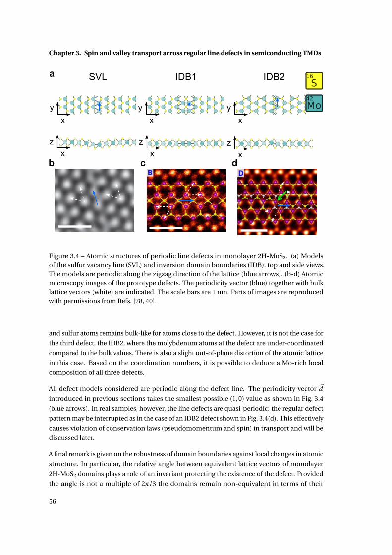
Chapter 3. Spin and valley transport across regular line defects in semiconducting TMDs
Figure 3.4 – Atomic structures of periodic line defects in monolayer 2H-MoS2. (a) Modelsof the sulfur vacancy line (SVL) and inversion domain boundaries (IDB), top and side views.The models are periodic along the zigzag direction of the lattice (blue arrows). (b-d) Atomicmicroscopy images of the prototype defects. The periodicity vector (blue) together with bulklattice vectors (white) are indicated. The scale bars are 1 nm. Parts of images are reproducedwith permissions from Refs. [78, 40].
and sulfur atoms remains bulk-like for atoms close to the defect. However, it is not the case for
the third defect, the IDB2, where the molybdenum atoms at the defect are under-coordinated
compared to the bulk values. There is also a slight out-of-plane distortion of the atomic lattice
in this case. Based on the coordination numbers, it is possible to deduce a Mo-rich local
composition of all three defects.
All defect models considered are periodic along the defect line. The periodicity vector ~d
introduced in previous sections takes the smallest possible (1,0) value as shown in Fig. 3.4
(blue arrows). In real samples, however, the line defects are quasi-periodic: the regular defect
pattern may be interrupted as in the case of an IDB2 defect shown in Fig. 3.4(d). This effectively
causes violation of conservation laws (pseudomomentum and spin) in transport and will be
discussed later.
A final remark is given on the robustness of domain boundaries against local changes in atomic
structure. In particular, the relative angle between equivalent lattice vectors of monolayer
2H-MoS2 domains plays a role of an invariant protecting the existence of the defect. Provided
the angle is not a multiple of 2π/3 the domains remain non-equivalent in terms of their
56

3.3. Ballistic transport across periodic line defects in a monolayer 2H-MoS2
orientation. Thus, the corresponding inversion domain boundary is guaranteed to exist and
the local changes of the atomic structure cannot terminate or eliminate the defect without
destroying one of the bulk crystals completely. Such topological protection is the case for
most of intrinsic line defects in monolayer 2H-MoS2 and inversion domain boundaries in
particular. In contrast, a pristine monolayer 2H-MoS2 flake can be recovered from the SVL
model by simply donating the missing sulfur atoms.
3.3 Ballistic transport across periodic line defects in a monolayer
2H-MoS2
The ballistic transport in monolayer 2H-TMDs is particularly interesting from the point of view
of interplay between conservation laws (energy, pseudomomentum, spin), the spin texture of
bulk bands and the spin-valley coupling. The simulations show that all (1,0) defects presented
in Fig. 3.4 are non-magnetic, thus, the whole setup is spin-neutral. This eliminates several spin
relaxation channels (spin waves, relaxation on local magnetic moments) suggesting a larger
spin lifetime in monolayer 2H-TMDs. On the other hand, the periodicity of defects imposes
certain conditions on the charge carrier pseudomomentum and, thus the valley index. Finally,
the whole picture is complemented by the spin-valley coupling discussed previously. The
excess of conditions to be satisfied may prohibit the charge carrier transmission at the level of
symmetries and may cause a transport gap.
3.3.1 The transport gap
To understand the role of the conservation laws in the charge carrier ballistic transport con-
sider 2 cases schematically illustrated in Fig. 3.5(a,b). The first case corresponds to, for example,
the SVL defect where the leads have a matching crystallographic orientation. There, the bal-
listic transport channels connect bulk wavefunctions with exactly the same spatial and spin
character. In particular, the transport channels corresponding to the K and K’ points of the BZ
transmit charge carriers without changing spin. However, provided the drain lead is rotated
with respect to the charge carrier source, the endpoint of the transmission channel is changed.
This generally reduces the transmission probability: naively, the overlap between incoming
and transmitted states becomes non-unity. In the case of IDBs, however, the reduction of
transmission probability is exaggerated up to no charge carrier transmission at all because the
single-particle bulk states corresponding the channel are orthogonal in the spin space. This
is schematically illustrated in Fig. 3.5(b) where the same channel connects bulk states with
different spin and valley character. An alternative point of view on this process is following:
the rotation of one of the leads in real space causes rotation of the corresponding BZ such that
the K and K’ points are swapped. The charge carriers, however, tend to conserve their spin
and, thus the valley due to the spin-valley coupling. The conflict between these two processes
prohibits charge carrier transport.
57

Chapter 3. Spin and valley transport across regular line defects in semiconducting TMDs
Figure 3.5 – The transport gap for charge carriers travelling across line defects. (a) A schematicillustration of a non-topological line defect (top) and the corresponding band diagram of thecharge carrier transmission (bottom). The matching colors in the bottom panel indicate thevalue of spin polarization of the two topmost valence bands in leads. The arrows indicateallowed charge carrier transport channels. (b) The topological line defect case. The oppositeorientations of bulk lattices in the top panel cause mismatch of spin in transport indicated withcolors in the bottom panel. The crossed arrows indicate closed ballistic transport channels.
The above transport gap argument can be summarized in the following picture of the electronic
band structure of a defect. Consider a defect with a periodicity vector ~d . This vector can be
expressed as a sum of bulk unit vectors ~a,~b with integer pre-factors n,m for both left (L) and
right (R) leads:
~d = nL~aL +mL~bL = nR~aR +mR
~bR . (3.1)
The periodicity vector ~d in the real space defines the 1D Brillouin zone of the defect. The
only coordinate of the reciprocal space of the defect is the aforementioned projection of the
pseudomomentum k||. To discover the spin-conserving and spin-flip channels one projects
the leads’ modes onto the 1D BZ, see Appendix A.5 for the details. Examples of such projection
for both leads are demonstrated in Fig. 3.6. While the Γ point can be projected onto k|| = 0 only,
there are several possibilities for other high-symmetry points K and K’. They can be projected
58

3.3. Ballistic transport across periodic line defects in a monolayer 2H-MoS2
Figure 3.6 – A schematic illustration of bulk states of a monolayer 2H-MoS2 in the leadsprojected onto the 1D BZ of the defect. The color indicates spin polarization of states at agiven E , k||: red and blue are spin-up and spin-down states only while magenta indicates thatstates with both spin polarization are available. (a) The case of a small defect periodicity vectorwith a large 1D BZ. (b) The case of a large defect periodicity vector with a small 1D BZ. Thetransport gap Et is indicated in both cases.
either onto ± 4π3d or onto Γ, depending on n and m (d =
∣∣∣~d ∣∣∣):
(n −m) mod 3 = 0 : k|| (K) = k|| (Γ) = 0 ;
(n −m) mod 3 = 1 : k|| (K) = 2π3d ;
(n −m) mod 3 =−1 : k|| (K) =− 2π3d .
(3.2)
The transport gap occurrs if
(nL −mL) mod 3 6= (nR −mR ) mod 3 , (3.3)
i.e. if K valleys hosting spin-up states from different leads are projected differently. The
resulting magnitude of the transport gap Et is defined as the maximum possible energy where
the charge carrier transmission is restored:
Et = min
[∆ESO,∆EK−Γ,
h2
72m?a2
a
d
], (3.4)
where the effective mass of charge carriers m?, the lattice constant a and the Planck constant
h are included. The details of the above expression can also be found in Appendix A.5.
The Eq. 3.4 claims the transport gap to be inversely proportional to the defect periodicity d .
59
Chapter 3. Spin and valley transport across regular line defects in semiconducting TMDs
This is a formal illustration of the fact that in the limit of a non-periodic line defect when
d →+∞ the pseudomomentum is not conserved, thus, the charge carriers are always allowed
to scatter to the preferred valley hosting bulk states with the spin required. The intermediate
case of a large but finite d is illustrated in Fig. 3.6(b). There, the BZ gets smaller while the
valleys effectively overlap more allowing an intra-valley scattering at energies close to the
Fermi level.
Another remark is related to the Γ valley where bulk states are spin-degenerate. As illustrated
in Fig. 3.6(a) the highest-energy states at the Γ valley set the lower limit for the transport gap,
though, according to band structures presented in Fig. 3.2 it is not a relevant factor in both
selenides and tellurides where ∆ESO <∆EK−Γ.
The discussion above is based on the fact that the non-magnetic defects do conserve spin of
charge carriers. This is not exactly true: there is an out-of-plane easy axis for charge carrier
spins in monolayer 2H-TMDs. If the defect is bent, the axis is changed accordingly to match
the local effective plane of a monolayer material. For example, both SVL and IDB2 defects
in Fig. 3.4 are subjects to out-of-plane deformations. Thus, a charge carrier approaching
these defects with an out-of-plane spin will form a non-zero overlap with charge carriers from
the opposite valley with an opposite spin due to spin precession around a local easy axis.
The non-zero overlap between spin states assists charge carrier transmission via a spin-flip
channel which is otherwise closed. The ab-initio simulations presented further provide a
qualitative measure to this effect.
3.3.2 Transport simulations and the spin polarization of charge carrier current
As outlined in the beginning of this chapter, the valley and, thus, spin polarization of charge
carriers in monolayer 2H-MoS2 can be induced by light. Another opportunity to induce
the valley polarization using transport across line defects was suggested for graphene[73].
There, otherwise equivalent valleys are discriminated by allowing ballistic currents to cross
the periodic line defect at oblique angles. This results in the valley polarization of the current
flowing across the defect. In monolayer 2H-TMDs, the valley polarization of hole charge
carriers is equivalent to the spin polarization due to the spin-valley coupling. Thus, a similar
setup in monolayer 2H-TMDs is expected to give rise to spin currents (the physical background
of the original proposal and its relevance to monolayer 2H-TMDs are given in Appendix A.2).
The argument is supported by the results of ab-initio transport simulations presented in this
section.
In particular, three defects from Fig. 3.4 were considered. Each defect was relaxed following the
NEGF1 transport simulations described in the previous chapter. Other details of simulations
are given in Appendix A.3.
1While the NEGF abbreviation stands for the non-equilibrium Green’s function the actual calculations werecarried out under zero voltage bias which may be viewed as an equilibrium setup.
60
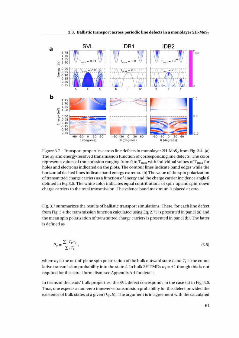
3.3. Ballistic transport across periodic line defects in a monolayer 2H-MoS2
Figure 3.7 – Transport properties across line defects in monolayer 2H-MoS2 from Fig. 3.4. (a)The k|| and energy-resolved transmission function of corresponding line defects. The colorrepresents values of transmission ranging from 0 to Tmax with individual values of Tmax forholes and electrons indicated on the plots. The contour lines indicate band edges while thehorizontal dashed lines indicate band energy extrema. (b) The value of the spin polarizationof transmitted charge carriers as a function of energy and the charge carrier incidence angle θdefined in Eq. 3.5. The white color indicates equal contributions of spin-up and spin-downcharge carriers to the total transmission. The valence band maximum is placed at zero.
Fig. 3.7 summarizes the results of ballistic transport simulations. There, for each line defect
from Fig. 3.4 the transmission function calculated using Eq. 2.75 is presented in panel (a) and
the mean spin polarization of transmitted charge carriers is presented in panel (b). The latter
is defined as
Pσ =∑
i Tiσi∑i Ti
, (3.5)
where σi is the out-of-plane spin polarization of the bulk outward state i and Ti is the cumu-
lative transmission probability into the state i . In bulk 2H TMDs σi =±1 though this is not
required for the actual formalism, see Appendix A.4 for details.
In terms of the leads’ bulk properties, the SVL defect corresponds to the case (a) in Fig. 3.5.
Thus, one expects a non-zero transverse transmission probability for this defect provided the
existence of bulk states at a given (k||,E). The argument is in agreement with the calculated
61
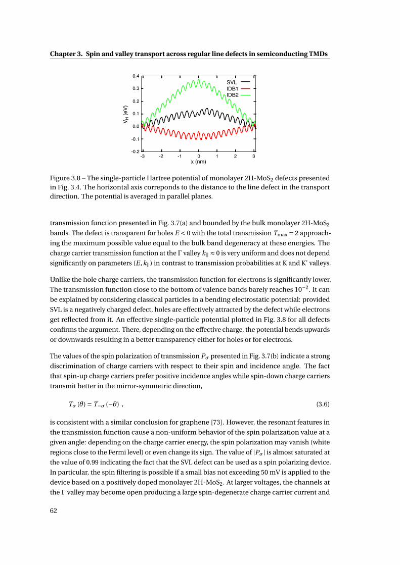
Chapter 3. Spin and valley transport across regular line defects in semiconducting TMDs
-3 -2 -1 0 1 2 3x (nm)
-0.2
-0.1
0.0V H
(eV)
0.1
0.2
0.3
0.4SVLIDB1IDB2
Figure 3.8 – The single-particle Hartree potential of monolayer 2H-MoS2 defects presentedin Fig. 3.4. The horizontal axis correponds to the distance to the line defect in the transportdirection. The potential is averaged in parallel planes.
transmission function presented in Fig. 3.7(a) and bounded by the bulk monolayer 2H-MoS2
bands. The defect is transparent for holes E < 0 with the total transmission Tmax = 2 approach-
ing the maximum possible value equal to the bulk band degeneracy at these energies. The
charge carrier transmission function at the Γ valley k|| ≈ 0 is very uniform and does not depend
significantly on parameters (E ,k||) in contrast to transmission probabilities at K and K’ valleys.
Unlike the hole charge carriers, the transmission function for electrons is significantly lower.
The transmission function close to the bottom of valence bands barely reaches 10−2. It can
be explained by considering classical particles in a bending electrostatic potential: provided
SVL is a negatively charged defect, holes are effectively attracted by the defect while electrons
get reflected from it. An effective single-particle potential plotted in Fig. 3.8 for all defects
confirms the argument. There, depending on the effective charge, the potential bends upwards
or downwards resulting in a better transparency either for holes or for electrons.
The values of the spin polarization of transmission Pσ presented in Fig. 3.7(b) indicate a strong
discrimination of charge carriers with respect to their spin and incidence angle. The fact
that spin-up charge carriers prefer positive incidence angles while spin-down charge carriers
transmit better in the mirror-symmetric direction,
Tσ (θ) = T−σ (−θ) , (3.6)
is consistent with a similar conclusion for graphene [73]. However, the resonant features in
the transmission function cause a non-uniform behavior of the spin polarization value at a
given angle: depending on the charge carrier energy, the spin polarization may vanish (white
regions close to the Fermi level) or even change its sign. The value of |Pσ| is almost saturated at
the value of 0.99 indicating the fact that the SVL defect can be used as a spin polarizing device.
In particular, the spin filtering is possible if a small bias not exceeding 50 mV is applied to the
device based on a positively doped monolayer 2H-MoS2. At larger voltages, the channels at
the Γ valley may become open producing a large spin-degenerate charge carrier current and
62
3.4. Ballistic transport across inversion domain boundary in monolayer 2H-MoSe2
resulting in a much lower value of |Pσ|. It is also possible to achieve significant values of Pσ for
electron charge carriers though the transparency of the defect in this case is much lower.
Unlike the SVL defect, both IDBs satisfy Eq. 3.3 and, thus, correspond to the transport gap
case schematically illustrated in Fig. 3.5. Thus, there is no transport of low-energy hole charge
carriers in this case. The argument is in agreement with the corresponding simulation results
presented in Fig. 3.7(a). Deeper in the valence energy region spin-conserving channels become
available and the charge carrier transmission is restored there. The relevant channels releasing
the ballistic transport regime are first found at the Γ valley for the IDB2 defect while in the
case of IDB1 the transmission probabilities there are relatively low.
The aforementioned transport gap is reproduced perfectly for the IDB1 defect. Instead, the
IDB2 case shows a small residual transmission in the energy gap region presented in Fig. 3.7(a).
There, the spin-flip transmission channels are open. As discussed, both defects are non-
magnetic, however, the IDB2 defect violates the out-of-plane direction as an easy spin axis due
to bending of the defect structure. The bulk spin-up and spin-down states become coupled in
this case.
One more feature related to the charge carrier transport is the fact that the IDB1 and the
IDB2 defects accumulate opposite effective charges. The over-coordinated sulfur atoms in
the first case gain an additional positive charge while under-coordinated molybdenum atoms
in the second defect are charged negatively compared to their bulk counterparts. This is in
agreement with the single-particle potential profiles presented in Fig. 3.8.
3.4 Ballistic transport across inversion domain boundary in mono-
layer 2H-MoSe2
As a part of a joint project together with experimental groups of Ute Kaiser at the University of
Ulm and Andras Kis at EPFL as well as the theoretical group of Arkady V. Krasheninnikov at
the Aalto University the transport properties of an inversion domain boundary in monolayer
2H-MoSe2 were studied. The defective material exhibited crystalline monolayer 2H-MoSe2
flakes with various orientations separated by ordered line defects as shown in the microscopy
images in Fig. 3.9. Among the line defects observed are the simplest (1,0) inversion domain
boundary shown in Fig. 3.9(b) and small-angle domain boundaries presented in the original
work[80]. The inversion domain boundary is similar to the IDB1 defect considered in the
previous section for a monolayer 2H-MoS2. Thus, similar transport properties are expected.
To verify this, the NEGF calculations have been carried out of the relaxed defect model.
The resulting transmission function, Fig. 3.10(a), and the potential profile, Fig. 3.10(b) strongly
resemble those of the monolayer 2H-MoS2 IDB1 model presented in Figs. 3.7(a),3.8. The
atomic structure of the defect presented in Fig. 3.10(b) does not show any new qualitative fea-
tures either. Both defects are charged positively resulting in a better transmission probability
for electrons. Similarly to the defect in monolayer 2H-MoS2, transmission probabilities at the
63

Chapter 3. Spin and valley transport across regular line defects in semiconducting TMDs
Figure 3.9 – Atomic microscopy images of defective monolayer 2H-MoSe2 showing polycrys-talline structure of the sample. (a) A large-scale microscopy image of monolayer 2H-MoSe2.The different colors correspond to different crystallographic orientations of monolayer 2H-MoSe2 grains. (b) Inversion domain boundary in monolayer 2H-MoSe2 imaged. A schematicatomic structure is overlaid.
Figure 3.10 – Electronic and transport properties of an inversion domain boundary in MoSe2.(a) k||-resolved transmission function values (left) and the integrated transmission (right) as afunction of a charge carrier energy E . (b) The single-particle Hartree potential profile acrossthe inversion domain boundary averaged over planes. The top view of the relaxed atomicstructure is also shown.
Γ valley for the monolayer 2H-MoSe2 model are rather small. The expected transport gap in
these calculations that did not focus on spin- and valley-polarized transport is not captured
by the model: the spin degree of freedom for the Kohn-Sham wavefunction was ignored in
favor of simplicity of the description. According to Eq. 3.4 as well as the bulk band structure
data presented in Fig. 3.2 the magnitude of the transport gap expected in monolayer MoSe2 is
rather defined by the spin-orbit splitting value ∆ESO = 184 meV being smaller than the value
of ∆Ek−Γ for this material.
To summarize, the inversion domain boundary defects in monolayer monolayer 2H-MoS2
and MoSe2 are very similar from the point of view of electronic and transport properties.
The simulations do not show any qualitative differences between the defect models despite
being done at a slightly different methodological level. Nevertheless, the transport gap in a
monolayer 2H-MoSe2 is expected to be substationally larger compared to the one in monolayer
64
3.5. Conclusions
2H-MoS2 due to lower energies of holes at the Γ valley. This also suggests better spin filtering
capabilities of a monolayer 2H-MoSe2 where the spin-degenerate ballistic charge carrier
current originating from the Γ valley is irrelevant.
3.5 Conclusions
As demonstrated, the ballistic charge carrier transport across periodic line defects in a mono-
layer 2H-MoS2 is governed by several conservation laws. The conservation of spin together
with the spin-valley coupling cause charge carrier transport properties to be strongly discrimi-
nated with respect to the spin value. For non-topological defects, high spin polarization of
charge carrier currents are predicted. For inversion domain boundaries, the conservation
of spin causes suppression of spin-flip channels resulting in a transport gap extended into
the valence energy region. The defect orientation and periodicity plays a defining role in this
process. The electric charge accumulated on line defects causes discrimination of transmitted
charge carriers with respect to their energy. The conclusions are also applicable to other mono-
layer 2H-TMDs with qualitatively same structural and electronic properties. The transmission
probabilities obtained for an inversion domain boundary in monolayer 2H-MoSe2 show a
qualitatively same picture. Overall, the phenomena discussed may find applications in 2D
electronics and spintronics where line defects could constitute a lateral device.
65


4 Electronic properties of the distorted1T structural phase in monolayerTMDsThe 2H structural phase is the thermodynamically stable phase of monolayer MoS2, MoSe2,
MoTe2, WS2, WSe2. However, monolayer WTe2 as well as other monolayer TMDs such as ReS2
realize a different atomic structure. There, one of the chalcogen atoms shifts inside the unit
cell parallel to the material plane resulting in the 1T lattice structure presented in Fig. 4.1.
However, monolayer 1T-TMDs are usually not stable. They are subjects to a spontaneous
breaking of the translation symmetry accompanied by the formation of metallic zigzag chains
and a slight change of unit cell vectors. The resulting 1T’ lattice structure is illustrated in
Fig. 4.1.
The spontaneous breaking of the translation symmetry leading to the 1T’ phase may occur
along one of the three equivalent crystallographic directions of the hexagonal lattice. The
resulting 1T’ unit cell contains six atoms compared to three atoms in the unit cell of the
1T phase. The ratio between 1T’ lattice constants a and b shown in Fig. 4.1 resembles the
original hexagonal symmetry: a/b ≈p3. Unlike the original 2H lattice, both 1T and 1T’ lattice
structures contain inversion centers indicated in Fig. 4.1. Combined with the time reversal
symmetry preserved by the material, the inversion symmetry results in the two-fold spin
degeneracy of all bulk states in monolayer 1T’-TMDs.
Among the monolayer TMDs being discussed, the 1T’ phase is a ground state phase for
WTe2 only, however, other TMDs can be stabilized in this phase by n-doping the material via
lithium or sodium intercalation[82, 83, 84, 85]. Depending on the details of an experimental
realization, the undistorted 1T phase was also reported in observations[79, 86].
The monolayer 1T’ phase is widely discussed in terms of its electronic properties. Having
the same chemical composition, monolayer 1T’ TMDs make a good lateral contact with the
semiconducting monolayer 2H phase[87]: the low Schottky barrier at the interface results in a
high transparency of the junction to transverse charge carriers. A non-trivial band ordering
of the monolayer 1T’ phase[88] attracts interest in the topological insulator community. The
quantum spin Hall (QSH) phase predicted for the family of materials may find applications
provided the bulk band gap of the monolayer 1T’ phase is large enough. By the time of
67
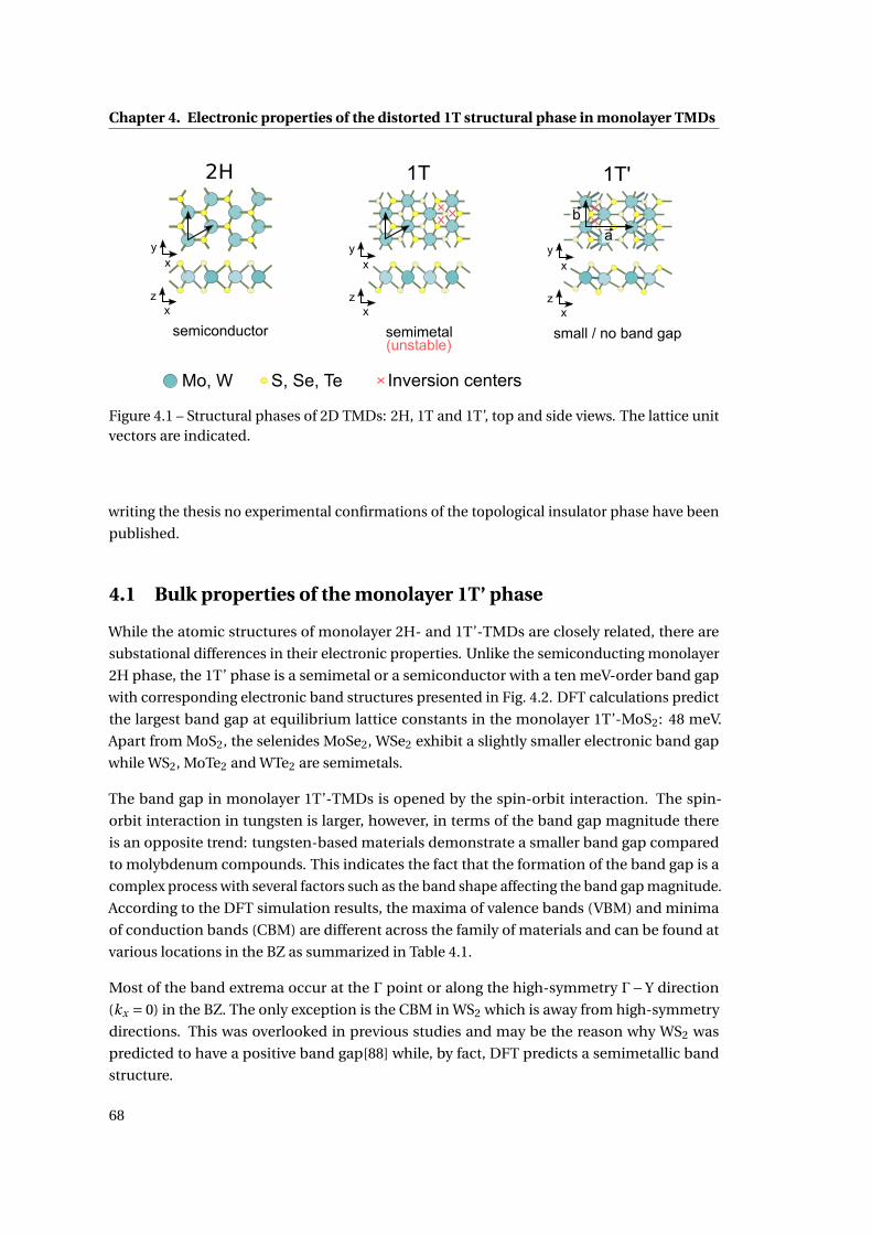
Chapter 4. Electronic properties of the distorted 1T structural phase in monolayer TMDs
Figure 4.1 – Structural phases of 2D TMDs: 2H, 1T and 1T’, top and side views. The lattice unitvectors are indicated.
writing the thesis no experimental confirmations of the topological insulator phase have been
published.
4.1 Bulk properties of the monolayer 1T’ phase
While the atomic structures of monolayer 2H- and 1T’-TMDs are closely related, there are
substational differences in their electronic properties. Unlike the semiconducting monolayer
2H phase, the 1T’ phase is a semimetal or a semiconductor with a ten meV-order band gap
with corresponding electronic band structures presented in Fig. 4.2. DFT calculations predict
the largest band gap at equilibrium lattice constants in the monolayer 1T’-MoS2: 48 meV.
Apart from MoS2, the selenides MoSe2, WSe2 exhibit a slightly smaller electronic band gap
while WS2, MoTe2 and WTe2 are semimetals.
The band gap in monolayer 1T’-TMDs is opened by the spin-orbit interaction. The spin-
orbit interaction in tungsten is larger, however, in terms of the band gap magnitude there
is an opposite trend: tungsten-based materials demonstrate a smaller band gap compared
to molybdenum compounds. This indicates the fact that the formation of the band gap is a
complex process with several factors such as the band shape affecting the band gap magnitude.
According to the DFT simulation results, the maxima of valence bands (VBM) and minima
of conduction bands (CBM) are different across the family of materials and can be found at
various locations in the BZ as summarized in Table 4.1.
Most of the band extrema occur at the Γ point or along the high-symmetry Γ−Y direction
(kx = 0) in the BZ. The only exception is the CBM in WS2 which is away from high-symmetry
directions. This was overlooked in previous studies and may be the reason why WS2 was
predicted to have a positive band gap[88] while, by fact, DFT predicts a semimetallic band
structure.
68

4.1. Bulk properties of the monolayer 1T’ phase
ky (2b )
1.0
0.5
0.0
0.5
1.0En
ergy
(eV)
MoS2
ky (2b )
MoSe2
ky (2b )
MoTe2
0.4 0.2 0.0 0.2 0.4ky (2
b )
1.0
0.5
0.0
0.5
1.0
Ener
gy (e
V)
WS2
0.4 0.2 0.0 0.2 0.4ky (2
b )
WSe2
0.4 0.2 0.0 0.2 0.4ky (2
b )
WTe2
YX A
ky
kx
Figure 4.2 – Electronic band structures of monolayer 1T’-TMDs projected onto the largestreciprocal vector ky . Colors are used to indicate high-symmetry paths Y−Γ−Y (red) andA−X−A (green) shown on the inset illustrating the rectangular BZ.
Table 4.1 – Properties of a band gap in monolayer 1T’-TMDs: locations of band extrema(VBM,CBM), magnitudes of the band gap Eg and magnitudes of the band gap at the Γ point∆Γ.
MoS2 MoSe2 MoTe2 WS2 WSe2 WTe2
CBM Γ−Y Γ−Y Γ−Y elsewhere Γ−Y Γ−YVBM Γ−Y Γ−Y Γ Γ Γ (flat band) Γ
insulator 3 3 7 7 3 7
Eg (meV) 48 35 −184 −44 29 −84∆Γ (meV) 500 780 543 125 649 1017
In semimetals, the band extrema correspond to the location of hole and electron pockets in
the 2D BZ shown in Fig. 4.3. There, WS2 indeed shows 4 relatively small symmetric electron
pockets and a single hole pocket at the Γ point. Two larger electron pockets are predicted for
MoTe2 and WTe2 showing similar behavior in terms of electronic band strcutres.
Semiconducting monolayer 1T’-TMDs were predicted to be topological insulators[88] in the
non-trivial QSH phase. The corresponding topological invariant classifies band insulators
under the time-reversal symmetry and takes two possible values ν=±1 depending on whether
the band order is vacuum-like, ν = 1, or not, ν = −1. The bulk-boundary correspondence
discussed previously induces at least two gapless modes at the edge of a topological insulator
or wherever the topological phase changes. The edge modes of the QSH phase are time-
reversal-symmetric and usually have opposite spins. This causes various phenomena specific
to the boundary of the QSH phase such as the spin-momentum locking or Majorana fermion
69
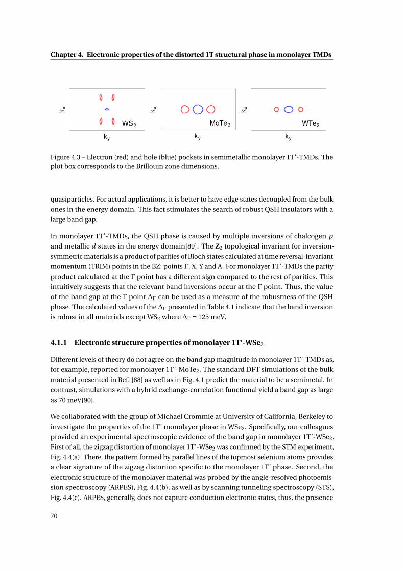
Chapter 4. Electronic properties of the distorted 1T structural phase in monolayer TMDs
ky
k x
WS2
ky
k x
MoTe2
ky
k x
WTe2
Figure 4.3 – Electron (red) and hole (blue) pockets in semimetallic monolayer 1T’-TMDs. Theplot box corresponds to the Brillouin zone dimensions.
quasiparticles. For actual applications, it is better to have edge states decoupled from the bulk
ones in the energy domain. This fact stimulates the search of robust QSH insulators with a
large band gap.
In monolayer 1T’-TMDs, the QSH phase is caused by multiple inversions of chalcogen p
and metallic d states in the energy domain[89]. The Z2 topological invariant for inversion-
symmetric materials is a product of parities of Bloch states calculated at time reversal-invariant
momentum (TRIM) points in the BZ: points Γ, X, Y and A. For monolayer 1T’-TMDs the parity
product calculated at the Γ point has a different sign compared to the rest of parities. This
intuitively suggests that the relevant band inversions occur at the Γ point. Thus, the value
of the band gap at the Γ point ∆Γ can be used as a measure of the robustness of the QSH
phase. The calculated values of the ∆Γ presented in Table 4.1 indicate that the band inversion
is robust in all materials except WS2 where ∆Γ = 125 meV.
4.1.1 Electronic structure properties of monolayer 1T’-WSe2
Different levels of theory do not agree on the band gap magnitude in monolayer 1T’-TMDs as,
for example, reported for monolayer 1T’-MoTe2. The standard DFT simulations of the bulk
material presented in Ref. [88] as well as in Fig. 4.1 predict the material to be a semimetal. In
contrast, simulations with a hybrid exchange-correlation functional yield a band gap as large
as 70 meV[90].
We collaborated with the group of Michael Crommie at University of California, Berkeley to
investigate the properties of the 1T’ monolayer phase in WSe2. Specifically, our colleagues
provided an experimental spectroscopic evidence of the band gap in monolayer 1T’-WSe2.
First of all, the zigzag distortion of monolayer 1T’-WSe2 was confirmed by the STM experiment,
Fig. 4.4(a). There, the pattern formed by parallel lines of the topmost selenium atoms provides
a clear signature of the zigzag distortion specific to the monolayer 1T’ phase. Second, the
electronic structure of the monolayer material was probed by the angle-resolved photoemis-
sion spectroscopy (ARPES), Fig. 4.4(b), as well as by scanning tunneling spectroscopy (STS),
Fig. 4.4(c). ARPES, generally, does not capture conduction electronic states, thus, the presence
70

4.1. Bulk properties of the monolayer 1T’ phase
of the band gap cannot be deduced from Fig. 4.4(b) directly. Instead, the STS data clearly
shows a deep depression close to the Fermi level in Fig. 4.4(c).
Figure 4.4 – Experimental observation of the monolayer 1T’ phase in WSe2. (a) STM imageof the monolayer 1T’-WSe2. The high-contrast regions correspond to the topmost chainsof selenium atoms. (b) Angle-resolved photoemission spectroscopy (ARPES) data of themonolayer 1T’-WSe2 electronic structure in the valence energy region. The correspondingcalculated bulk bands are overlaid. The white arrow indicated two minima of conductionbands (two electron pockets in experiment) connected with a nesting vector. (c) The scanningtunneling spectroscopy (STS) data of the monolayer material (experiment) compared to thecalculated density of states (theory). (d) The quasiparticle interference pattern measured forthe monolayer 1T’-WSe2 at energies 100 meV above the top of the valence bands. The Brillouinzone is marked by a yellow frame. The corresponding simulated interference signal is shownin the green frame.
To support the experimental observations, I performed calculations of electronic band struc-
ture properties of the monolayer 1T’-WSe2 using DFT. Specifically, the electronic band struc-
ture, the density of electronic states and the autocorrelation function of the band structure in
k-space were computed to compare to the experimental data.
71

Chapter 4. Electronic properties of the distorted 1T structural phase in monolayer TMDs
As introduced in the previous section, the monolayer 1T’-WSe2 is a semiconductor with a
30 meV band gap also present in the DOS plot in Fig. 4.4(c). The electronic band structure
showing the band gap location agrees well with the ARPES data, Fig. 4.4(b). The quasiparticle
interference (QPI) pattern gives an information on possible nesting vectors in the reciprocal
space of monolayer 1T’-WSe2. It provides an important information about the dispersion of
the conduction band. Practically, the QPI signal is as simple as a Fourier transform of the STS
data at a given energy. Thus, the corresponding theoretical analogue can be obtained directly
from the calculated band structure as, for example, described in Ref. [91]. The QPI pattern
for monolayer 1T’-WSe2 is presented in Fig. 4.4(d). It strongly resembles the corresponding
simulated image (green frame) with 3 similar regions of a large signal displaced along the ky
reciprocal vector. The displacement roughly corresponds to the length of the reciprocal vector
connecting electron pockets shown in Fig. 4.4(b).
The combination of experimental and theoretical evidences allows one to conclude that
monolayer 1T’-WSe2 is indeed a semiconducting material in the QSH phase. The presence
of the band inversion at the Γ point is confirmed by the ARPES data being in agreement with
the theoretical predictions. During the theoretical ab-initio investigation of its properties,
however, it was found that the band gap obtained in the relaxed material is highly sensitive to
the level of methodology similar to the aforementioned issue of monolayer 1T’-MoTe2. The
closing of the band gap, however, may destroy the topological phase in the family of materials.
Thus, it is important to study possible mechanisms of the band gap closing and to investigate
inconsistencies between different methodologies.
Specifically, the variations of materials’ lattice parameters were found to have a major impact
on the presence and the magnitude of the band gap. The following section discusses the
electronic properties of monolayer 1T’-TMDs under strain from the theoretical perspective.
The study is also presented in Ref. [92].
4.1.2 Properties of monolayer 1T’-TMDs under strain
The monolayer 1T’-WSe2 discussed previously is a semiconductor under the DFT-PBE (Perdew-
Burke-Ernzerhof[93]) approach. The LDA exchange-correlation functional[94], however, re-
sults in a semimetallic band structure for this material. The major difference between simu-
lated electronic band structures may be due to the smaller unit cell predicted under the local
density approximation. This hypothesis was verified by performing simulations of electronic
properties of the four monolayer 1T’-TMDs: MoS2, MoSe2, WS2, WSe2 across the range of
lattice constants.
A series of DFT electronic structure simulations of monolayer 1T’-TMDs has been performed
with varying bulk lattice constants. The maximum deviation of lattice constants was set to
5% of the equilibrium values predicted at the PBE level of theory. The whole range of lattice
constants was sampled on a 19x19 mesh. At each point of the lattice parameter space, atomic
structures of bulk materials were relaxed and electronic band structures were calculated on a
72
4.1. Bulk properties of the monolayer 1T’ phase
60x90 k-point grid to capture the band gap location and magnitude accurately. Additionally,
equilibrium structural and electronic properties were calculated for both LDA and PBEsol[95]
exchange-correlation functionals. The latter is commonly used for a more accurate description
of structural and electronic properties of 3D materials’ surfaces and 2D materials.
The calculated magnitude of the band gap is presented in Fig. 4.5(a-d). The former is found
to be sensitive to lattice constants in all four materials. The semiconducting phase spans an
island-like region in the lattice parameter space. Thus, a relatively small deformation may
close the band gap in monolayer 1T’-TMDs. The required deviations from equilibrium PBE
lattice constants may be as small as 0.5% in the case of monolayer 1T’-WSe2 or as large as 4%
in the case of monolayer 1T’-MoS2.
The difference in predicted lattice constants between methodologies, however, is larger, as in-
dicated in Fig. 4.5(a-d). This results in the aforementioned inconsistency between predictions.
Specifically, the exchange-correlation functionals considered agree in terms of the band gap
magnitude only for monolayer 1T’-WS2 where semimetallicity is predicted. Otherwise LDA
always predicts a material to be a semimetal while PBE claims semiconductivity. According to
Fig. 4.5, the PBEsol exchange-correlation functional results in intermediate lattice constants
corresponding to either a finite band gap or no band gap depending on the material. The
problem of inconsistency between predictions of the band gap magnitude is resolved by cal-
culating the electronic band structure in a fixed unit cell using all three exchange-correlation
functionals. Such calculation yields surprisingly good agreement in terms of the band gap
magnitude. This confirms our initial hypothesis that the difference in values of the band gap
magnitude is mostly due to the difference between equilibrium lattice structures predicted
by exchange-correlation functionals. Thus, for a proper comparison with experimental data
experimental lattice structures should be used in DFT simulations.
For the possible applications of the QSH phase, one is interested in increasing the magnitude
of the bulk band gap. According to Fig. 4.5, the bulk band gap can be increased by applying
strain. A moderate strain along the largest lattice vector a may tune the band gap magnitude
in monolayer 1T’-MoS2 to slighty larger magnitudes up to 57 meV. Though the predicted band
gap magnitude in non-strained monolayer 1T’-TMDs is maximal in MoS2, other materials of
the family exhibit larger band gap magnitudes with the strain applied. According to Fig. 4.5(d)
a band gap as large as 120 meV is found in strained monolayer 1T’-WSe2. The maximal band
gap encountered in monolayer 1T’-MoSe2 is 30 meV smaller and requires larger deformations,
though, this value is not saturated. To open the band gap in monolayer 1T’-WS2 a compressive
strain is required which may limit applications of the gapped phase in this material. Otherwise
the maximal band gap magnitude in monolayer 1T’-WS2, 63 meV, is comparable to the one in
monolayer 1T’-MoS2.
The mechanism of a semiconductor-semimetal transition in the materials depends on the
direction of strain. Fig. 4.5(e) illustrates electronic band structures of monolayer 1T’-MoS2 as
an example. There, the band gap closing occurs at various points of the BZ. The monolayer
73
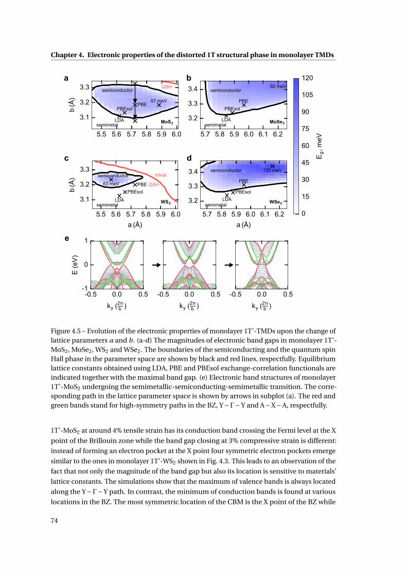
Chapter 4. Electronic properties of the distorted 1T structural phase in monolayer TMDs
5.5 5.6 5.7 5.8 5.9 6.0
3.1
3.2
3.3
b(Å
)
semimetal
semiconductor
MoS2
PBE57 meV
LDA
PBEsol
QSHa
5.7 5.8 5.9 6.0 6.1 6.2
3.2
3.3
3.4
semimetal
semiconductor
MoSe2
PBE
92 meV
LDA
PBEsol
b
5.5 5.6 5.7 5.8 5.9 6.0a (Å)
3.1
3.2
3.3
b(Å
)
semimetal
semiconductor
WS2
PBE63 meV
LDA
PBEsolQSH
trivial
c
5.7 5.8 5.9 6.0 6.1 6.2a (Å)
3.2
3.3
3.4
semimetal
semiconductor
WSe2
PBE
120 meV
LDAPBEsol
d
-0.5 0.0 0.5ky (2
b )
-1
0
1
E (e
V)
e
-0.5 0.0 0.5ky (2
b )-0.5 0.0 0.5
ky (2b )
0
15
30
45
60
75
90
105
120
Eg,
meV
Figure 4.5 – Evolution of the electronic properties of monolayer 1T’-TMDs upon the change oflattice parameters a and b. (a-d) The magnitudes of electronic band gaps in monolayer 1T’-MoS2, MoSe2, WS2 and WSe2. The boundaries of the semiconducting and the quantum spinHall phase in the parameter space are shown by black and red lines, respectfully. Equilibriumlattice constants obtained using LDA, PBE and PBEsol exchange-correlation functionals areindicated together with the maximal band gap. (e) Electronic band structures of monolayer1T’-MoS2 undergoing the semimetallic-semiconducting-semimetallic transition. The corre-sponding path in the lattice parameter space is shown by arrows in subplot (a). The red andgreen bands stand for high-symmetry paths in the BZ, Y−Γ−Y and A−X−A, respectfully.
1T’-MoS2 at around 4% tensile strain has its conduction band crossing the Fermi level at the X
point of the Brillouin zone while the band gap closing at 3% compressive strain is different:
instead of forming an electron pocket at the X point four symmetric electron pockets emerge
similar to the ones in monolayer 1T’-WS2 shown in Fig. 4.3. This leads to an observation of the
fact that not only the magnitude of the band gap but also its location is sensitive to materials’
lattice constants. The simulations show that the maximum of valence bands is always located
along the Y−Γ−Y path. In contrast, the minimum of conduction bands is found at various
locations in the BZ. The most symmetric location of the CBM is the X point of the BZ while
74
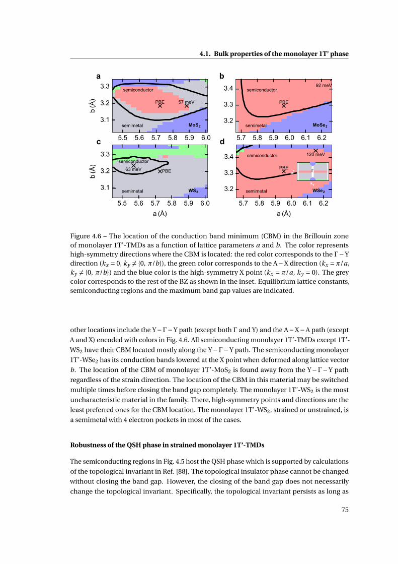
4.1. Bulk properties of the monolayer 1T’ phase
5.5 5.6 5.7 5.8 5.9 6.0
3.1
3.2
3.3b
(Å)
semimetal
semiconductor
MoS2
PBE 57 meV
a
5.7 5.8 5.9 6.0 6.1 6.2
3.2
3.3
3.4
semimetal
semiconductor
MoSe2
PBE
92 meV
b
5.5 5.6 5.7 5.8 5.9 6.0a (Å)
3.1
3.2
3.3
b(Å
)
semimetal
semiconductor
WS2
PBE63 meV
c
5.7 5.8 5.9 6.0 6.1 6.2a (Å)
3.2
3.3
3.4
semimetal
semiconductor
WSe2
PBE
120 meV
d
ky
k x
Figure 4.6 – The location of the conduction band minimum (CBM) in the Brillouin zoneof monolayer 1T’-TMDs as a function of lattice parameters a and b. The color representshigh-symmetry directions where the CBM is located: the red color corresponds to the Γ−Ydirection (kx = 0, ky 6= {0, π/b}), the green color corresponds to the A−X direction (kx =π/a,ky 6= {0, π/b}) and the blue color is the high-symmetry X point (kx = π/a, ky = 0). The greycolor corresponds to the rest of the BZ as shown in the inset. Equilibrium lattice constants,semiconducting regions and the maximum band gap values are indicated.
other locations include the Y−Γ−Y path (except both Γ and Y) and the A−X−A path (except
A and X) encoded with colors in Fig. 4.6. All semiconducting monolayer 1T’-TMDs except 1T’-
WS2 have their CBM located mostly along the Y−Γ−Y path. The semiconducting monolayer
1T’-WSe2 has its conduction bands lowered at the X point when deformed along lattice vector
b. The location of the CBM of monolayer 1T’-MoS2 is found away from the Y−Γ−Y path
regardless of the strain direction. The location of the CBM in this material may be switched
multiple times before closing the band gap completely. The monolayer 1T’-WS2 is the most
uncharacteristic material in the family. There, high-symmetry points and directions are the
least preferred ones for the CBM location. The monolayer 1T’-WS2, strained or unstrained, is
a semimetal with 4 electron pockets in most of the cases.
Robustness of the QSH phase in strained monolayer 1T’-TMDs
The semiconducting regions in Fig. 4.5 host the QSH phase which is supported by calculations
of the topological invariant in Ref. [88]. The topological insulator phase cannot be changed
without closing the band gap. However, the closing of the band gap does not necessarily
change the topological invariant. Specifically, the topological invariant persists as long as
75
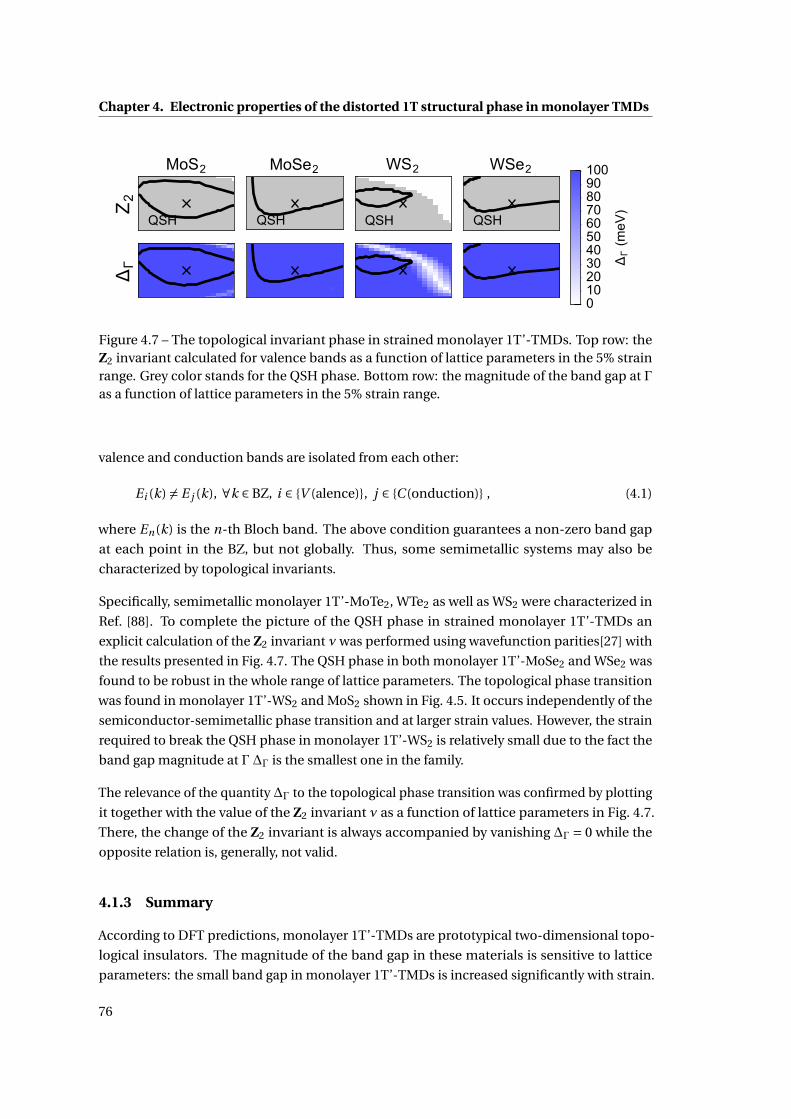
Chapter 4. Electronic properties of the distorted 1T structural phase in monolayer TMDs
QSH
Z 2
MoS2
QSH
MoSe2
QSH
WS2
QSH
WSe2
0102030405060708090100
(meV
)
Figure 4.7 – The topological invariant phase in strained monolayer 1T’-TMDs. Top row: theZ2 invariant calculated for valence bands as a function of lattice parameters in the 5% strainrange. Grey color stands for the QSH phase. Bottom row: the magnitude of the band gap at Γas a function of lattice parameters in the 5% strain range.
valence and conduction bands are isolated from each other:
Ei (k) 6= E j (k), ∀k ∈ BZ, i ∈ {V (alence)}, j ∈ {C (onduction)} , (4.1)
where En(k) is the n-th Bloch band. The above condition guarantees a non-zero band gap
at each point in the BZ, but not globally. Thus, some semimetallic systems may also be
characterized by topological invariants.
Specifically, semimetallic monolayer 1T’-MoTe2, WTe2 as well as WS2 were characterized in
Ref. [88]. To complete the picture of the QSH phase in strained monolayer 1T’-TMDs an
explicit calculation of the Z2 invariant ν was performed using wavefunction parities[27] with
the results presented in Fig. 4.7. The QSH phase in both monolayer 1T’-MoSe2 and WSe2 was
found to be robust in the whole range of lattice parameters. The topological phase transition
was found in monolayer 1T’-WS2 and MoS2 shown in Fig. 4.5. It occurs independently of the
semiconductor-semimetallic phase transition and at larger strain values. However, the strain
required to break the QSH phase in monolayer 1T’-WS2 is relatively small due to the fact the
band gap magnitude at Γ ∆Γ is the smallest one in the family.
The relevance of the quantity ∆Γ to the topological phase transition was confirmed by plotting
it together with the value of the Z2 invariant ν as a function of lattice parameters in Fig. 4.7.
There, the change of the Z2 invariant is always accompanied by vanishing ∆Γ = 0 while the
opposite relation is, generally, not valid.
4.1.3 Summary
According to DFT predictions, monolayer 1T’-TMDs are prototypical two-dimensional topo-
logical insulators. The magnitude of the band gap in these materials is sensitive to lattice
parameters: the small band gap in monolayer 1T’-TMDs is increased significantly with strain.
76

4.2. Edges of monolayer 1T’-TMDs
The largest magnitude of the band gap obtained occurs in selenides. It is also possible to
close the band gap at various points in the BZ depending on the strain direction. The induced
electron pockets appear either along high-symmetry directions in the BZ or away from them.
The latter scenario was completely overlooked in previous studies where the band gap for
both relaxed and strained materials was determined from electronic band structures along
high-symmetry paths only. As a result, monolayer 1T’-WS2 was claimed to be a semiconductor
while, by fact, it is a semimetal. Moreover, the possibility for a strain-induced semiconducting
phase is very limited in this material. The band inversion at the Γ point was found to be
responsible for the QSH phase in all monolayer 1T’-TMDs. The observed topological strain-
induced phase transition is accompanied by the closing of the band gap at the corresponding
point.
4.2 Edges of monolayer 1T’-TMDs
The edges of a topologically non-trivial QSH phase in monolayer 1T’-TMDs may host topo-
logically protected boundary modes. They are characterized by various unique properties
such as protected charge carrier transport, the spin texture of states and Majorana fermions.
The local conditions at the boundary play a crucial role in the above properties. For example,
a termination carrying a non-zero magnetic moment breaks the topological protection and
the underlying time-reversal symmetry. The edge mode may also cross the Fermi level more
than once lifting protection of the charge carrier transport. Depending on the local atomic
structure of a termination, various scenarios can be realized. Thus, the study of electronic
properties of particular terminations is crucial for understanding how topological insulators
can be used in practice.
The suggested edges to consider are periodic terminations along the shortest lattice vector
in monolayer 1T’-TMDs: the zigzag edges. The latter include six different structures with a
(1,0) periodicity corresponding to balanced, metal-rich and chalcogen-rich conditions and
presented in Fig. 4.8(a). Within each pair, one of the structures is terminated closer to the
zigzag chain while the other one includes an additional metallic atom. To investigate possible
atomic reconstruction effects at the edges the structural relaxation calculations were carried
out. A brief summary of simulation details are given in Appendix A.6.
The relaxed structures presented in Fig. 4.8(a) demonstrate only slight distortions compared
to the bulk lattice. The most significant structural changes are found in balanced terminations
(1) and (2) as well as in the chalcogen-rich termination (c1) where chalcogen atoms at the
edge are undercoordinated. There is also a significant structural distortion at the metal-rich
termination (m1) where the 3 rows of metallic atoms clusterize.
The six terminations considered differ in their formation energies Eb defined as
Eb = 1
2
(Eribbon −NMµM −NCµC
), (4.2)
77
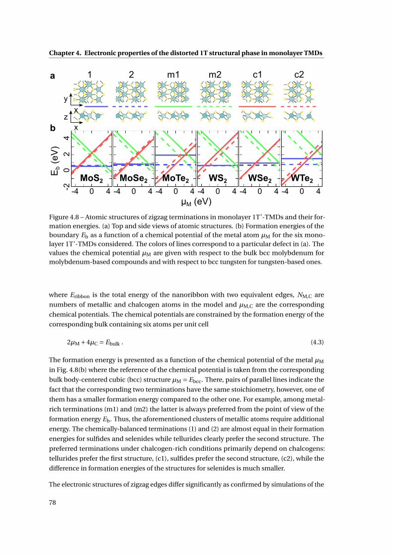
Chapter 4. Electronic properties of the distorted 1T structural phase in monolayer TMDs
Figure 4.8 – Atomic structures of zigzag terminations in monolayer 1T’-TMDs and their for-mation energies. (a) Top and side views of atomic structures. (b) Formation energies of theboundary Eb as a function of a chemical potential of the metal atom µM for the six mono-layer 1T’-TMDs considered. The colors of lines correspond to a particular defect in (a). Thevalues the chemical potential µM are given with respect to the bulk bcc molybdenum formolybdenum-based compounds and with respect to bcc tungsten for tungsten-based ones.
where Eribbon is the total energy of the nanoribbon with two equivalent edges, NM,C are
numbers of metallic and chalcogen atoms in the model and µM,C are the corresponding
chemical potentials. The chemical potentials are constrained by the formation energy of the
corresponding bulk containing six atoms per unit cell
2µM +4µC = Ebulk . (4.3)
The formation energy is presented as a function of the chemical potential of the metal µM
in Fig. 4.8(b) where the reference of the chemical potential is taken from the corresponding
bulk body-centered cubic (bcc) structure µM = Ebcc. There, pairs of parallel lines indicate the
fact that the corresponding two terminations have the same stoichiometry, however, one of
them has a smaller formation energy compared to the other one. For example, among metal-
rich terminations (m1) and (m2) the latter is always preferred from the point of view of the
formation energy Eb. Thus, the aforementioned clusters of metallic atoms require additional
energy. The chemically-balanced terminations (1) and (2) are almost equal in their formation
energies for sulfides and selenides while tellurides clearly prefer the second structure. The
preferred terminations under chalcogen-rich conditions primarily depend on chalcogens:
tellurides prefer the first structure, (c1), sulfides prefer the second structure, (c2), while the
difference in formation energies of the structures for selenides is much smaller.
The electronic structures of zigzag edges differ significantly as confirmed by simulations of the
78

4.2. Edges of monolayer 1T’-TMDs
-1
0
1
Ener
gy (e
V)
1Bala
nced
MoS2
2
MoSe2
2
MoTe2
2
WS2
2
WSe2
2
WTe2
-1
0
1
Ener
gy (e
V)
m2M-ri
ch
m2 m2 m2 m2 m2
0 1ky ( /b)
-1
0
1
Ener
gy (e
V)
c2C-ri
ch
0 1ky ( /b)
c10 1
ky ( /b)
c10 1
ky ( /b)
c20 1
ky ( /b)
c20 1
ky ( /b)
c1
Figure 4.9 – The k-resolved density of states localized at the energetically preferred zigzagterminations of the six monolayer 1T’-TMDs presented in Fig. 4.8. The blue and red colorsin each plot represent the contribution of out-of-plane spin-polarized states, spin-up andspin-down, to the total weight. The corresponding labels of atomic structures from Fig. 4.8are indicated in each plot. The full range of plots including non-preferred terminations ispresented in Appendix A.7.
local k-dependent density of electronic states presented in Fig. 4.9. The latter was calculated
as an imaginary part of the Green’s function trace from Eq. 2.67
n (E) =−Im Tr G (E) (4.4)
Up to eight spin-polarized modes are identified at the boundary. The character and the disper-
sion of edge modes depends on the termination structure. Thus, experimental observations
of the local electronic structure at the boundary, such as STS, may be able to identify the kind
of a boundary precisely. Specifically, chemically-balanced zigzag edges host only few modes
mostly away from the Fermi level. Instead, metal-rich boundaries demonstrate a rather high
density of electronic states close to the band gap. The electronic structure of a chalcogen-rich
termination in monolayer 1T’-TMDs depends on the kind of preferred termination: while
the (c1) termination hosts a pair of bands crossing the Fermi level, it is not the case for the
(c2) termination. Thus, the choice of a material also influences the electronic structure of a
boundary by means of the structure preferred. Provided the same atomic structure of the edge,
however, the electronic structures of different materials presented in Fig. 4.9 (see also Fig. A.3)
are very similar.
Most of the edge states are spin-polarized out of the material plane as indicated by color in
Fig. 4.9. The spin polarization is usually preserved along a particular band selected. Both
observations, however, are not the case for metal-rich termination (m2) especially in tungsten-
79

Chapter 4. Electronic properties of the distorted 1T structural phase in monolayer TMDs
Y Y-0.1
0.0
0.1
Ener
gy (e
V)
WSe2 (2)Y Y
WSe2 (c2)
Figure 4.10 – Momentum-resolved localized density of electronic states of zigzag terminationssuitable for the protected charge carrier ballistic transport experiment. The correspondingzigzag termination structure label is indicated in both plots. The horizontal lines are examplesof energies at which the ballistic charge carriers are protected from backscattering.
based compounds. There, pairs of bands in the conduction energy region become spin-
hybridized resulting in a non-uniform spin character of the band. The easy spin axis for
hybridized edge states is away from the normal direction.
The topologically protected spin modes are identified for all boundaries by the odd number
of Fermi level crossings. It is in agreement with the bulk-boundary correspondence of the
QSH phase. The time-reversal symmetry is preserved by all zigzag edges. Thus, no magnetic
moments are present and the spin degeneracy at TRIM points Γ and Y remains protected.
Depending on the particular dispersion of the edge modes, the edge may support protected
charge carrier ballistic transport. From this point of view, the most promising zigzag edges
are those of monolayer 1T’-WSe2 where two counter-propagating spin modes are present in
the bulk band gap energy region as shown in Fig. 4.10. For both chemically balanced and
chalcogen-rich terminations there exist ballistic charge carriers which are protected from
backscattering. To identify them, one has to choose the energy of charge carriers carefully as,
for example, illustrated by horizontal lines in Fig. 4.10. At the energies indicated, there exist
only two quasiparticles with opposite spins and group velocities. Spin-neutral perturbations
(such as local non-magnetic impurities, for example) do not couple these states. This, in
turn, results in a completely suppressed back-scattering of the edge charge carriers and the
protected charge carrier transport phenomena.
4.2.1 Summary
Periodic zigzag edges of monolayer 1T’-TMDs have been characterized in terms of structure,
formation energy and electronic properties. For each material, among six terminations consid-
ered, three have a lower formation energy. These edges host localized gapless modes protected
by the topologically non-trivial QSH phase and the underlying time-reversal symmetry. The
spin texture of the corresponding modes as well as the odd number of Fermi level crossings
80
4.3. Electronic properties of structural phase boundaries in monolayer WSe2
confirm that the states observed have a topological origin. As such, the protected charge
carrier transport becomes possible provided the material and the edge are chosen carefully.
Specifically, the two suggested zigzag edges in monolayer 1T’-WSe2 are prototypical ideal
nanowires where the charge carrier back-scattering is suppressed in a rather narrow energy
region inside the band gap.
4.3 Electronic properties of structural phase boundaries in mono-
layer WSe2
The topologically protected modes at the zigzag edges of monolayer 1T’-TMDs discussed
in the previous section indicate the change of the topological invariant when leaving a 2D
material bulk towards vacuum. The latter plays a role of a trivial insulating medium, however,
it can be replaced by any topologically trivial insulating material with a finite band gap. The
topologically protected edge states should persist as long as the trivial insulating material
respects the symmetries of the corresponding topological classification. For example, the 2H
structural phase of monolayer TMDs is in a trivial insulating QSH state under time-reversal
symmetry and can complement the 1T’ phase to induce topologically protected edge states.
The phase boundary between monolayer 2H- and 1T-TMDs prefers zigzag directions of the
crystal lattice according to several experimental studies[87, 79, 86]. Also, recently, multiple
2H-1T’ phase boundaries were observed in monolayer MoS2 separating strips of the two
phases parallel to the zigzag direction in the 2H phase[96]. The above studies mostly focus
on transverse transport properties of a 2D metal-insulator interface. A relatively low Schottky
potential barrier developed at the boundary allows an efficient injection of charge carriers
into the semiconducting 2H phase of the material compared to more common contacts to
gold or other bulk metals. The “patterning” of the metallic phase from the semiconducting 2H
phase in TMDs is a practical way to build a lateral 2D device which is a major advantage over
other materials.
The topological aspects of the phase boundary, however, have not yet been discussed. This
section is dedicated to electronic structure properties of 2H-1T’ interfaces in WSe2 – a rep-
resentative material where the band gap of the QSH phase can be tuned towards the largest
values in the family.
As discussed, the 1T’ phase of monolayer TMDs is formed from the stable 2H phase by shifting
one of the chalcogen planes towards the previously unoccupied high-symmetry position in the
hexagonal lattice. Thus, it is reasonable to expect that the lateral junction of the phases involves
only a minor distortion of the other two atomic planes. There are only several configurations
of a periodic phase boundary along the zigzag direction summarized in Fig. 4.11 where eight
possible relaxed phase boundary structures are presented. Among them, four structures
contain a 7-coordinated metal atom at the boundary (chalcogen-rich conditions) and four
other structures contain a 5-coordinated tungsten atom (metal-rich conditions). Another
81

Chapter 4. Electronic properties of the distorted 1T structural phase in monolayer TMDs
Figure 4.11 – Atomic structures of the 2H-1T’ phase boundaries along the zigzag directionof monolayer WSe2: top and side views. The colored line indicated tungsten-rich (blue) orselenium-rich (yellow) conditions.
degree of freedom to consider is the possibility to choose the crystallographic orientation
of the polar monolayer 2H-TMD: panels (1-4) in Fig. 4.11 contain atomic structures with
the same orientation of the monolayer 2H phase while panels (5-8) illustrate cases with the
opposite orientation. Lastly, the boundary may or may not contain unpaired metal atoms
which would otherwise form zigzag chains in the monolayer 1T’-phase1.
The starting point for the description of electronic properties of the interface is the relative
alignment of bulk bands presented in Fig. 4.12(a). In contrast to 3D materials, the band
alignments in 2D do not generally depend on the interface structure. Thus, the relative
alignment of bulk bands in 2D can be found by preforming bulk calculations and matching
the vacuum levels. In the case of WSe2, this results in a type-III heterojunction: the small band
gap of the 1T’ phase remains at lower energies and does not overlap with the band gap of the
2H monolayer phase. The supercell configurations with a phase boundary, however, result
in the Fermi level of the 1T’ phase material2 to be inside the band gap energy region of the
2H phase. The problem of the mismatch was previously reported for non-polar materials[97]
and, essentially, is due to long-range electrostatic potentials spanning the supercell model.
The weak logarithmic behavior of the potential prevents reasonably-sized supercell models to
correctly reproduce the bulk band alignment. In experimental setups, however, the long-range
potential is typically screened by localized charge carriers in the material or by the substrate.
The bulk states of both 2H and 1T’ monolayer phases can also be identified in Fig. 4.12(b)
where the local density of states at the phase boundary is presented. The overall picture of the
electronic structure is quite complicated since spin-degenerate bulk states of the 1T’ phase
overlap with spin-polarized bulk states of the 2H phase together with several spin modes
localized at the boundary. Compared to the “clean” bands presented in Fig. 4.10, neither of
1This possibility, however, may effectively result in a strain applied across the phase boundary: for example,atomic and electronic structures 1 and 3, 6 and 8 presented in Figs. 4.11, 4.12(b) respectfully are very similar.
2The Fermi level is fixed to the middle of a small band gap in monolayer 1T’-WSe2
82
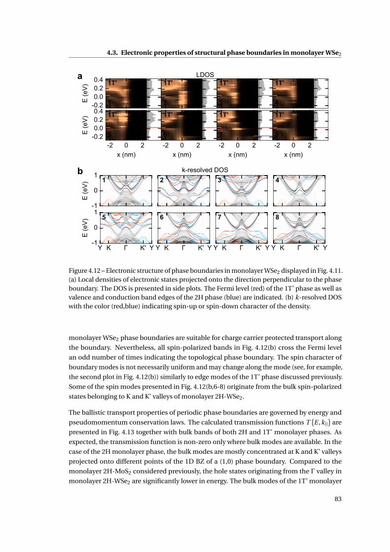
4.3. Electronic properties of structural phase boundaries in monolayer WSe2
-0.20.00.20.4
E (e
V)1T' 2H
1
a
-2 0 2x (nm)
-0.20.00.20.4
E (e
V)
1T' 2H
5
1T' 2H
2
-2 0 2x (nm)
1T' 2H
6
1T' 2H
3
-2 0 2x (nm)
1T' 2H
7
1T' 2H
4
-2 0 2x (nm)
1T' 2H
8
LDOS
-1
0
1
E (e
V)
1b
Y K K' Y-1
0
1
E (e
V)
5
2
Y K K' Y
6
3
Y K K' Y
7
4
Y K K' Y
8
k-resolved DOS
Figure 4.12 – Electronic structure of phase boundaries in monolayer WSe2 displayed in Fig. 4.11.(a) Local densities of electronic states projected onto the direction perpendicular to the phaseboundary. The DOS is presented in side plots. The Fermi level (red) of the 1T’ phase as well asvalence and conduction band edges of the 2H phase (blue) are indicated. (b) k-resolved DOSwith the color (red,blue) indicating spin-up or spin-down character of the density.
monolayer WSe2 phase boundaries are suitable for charge carrier protected transport along
the boundary. Nevertheless, all spin-polarized bands in Fig. 4.12(b) cross the Fermi level
an odd number of times indicating the topological phase boundary. The spin character of
boundary modes is not necessarily uniform and may change along the mode (see, for example,
the second plot in Fig. 4.12(b)) similarly to edge modes of the 1T’ phase discussed previously.
Some of the spin modes presented in Fig. 4.12(b,6-8) originate from the bulk spin-polarized
states belonging to K and K’ valleys of monolayer 2H-WSe2.
The ballistic transport properties of periodic phase boundaries are governed by energy and
pseudomomentum conservation laws. The calculated transmission functions T(E ,k||
)are
presented in Fig. 4.13 together with bulk bands of both 2H and 1T’ monolayer phases. As
expected, the transmission function is non-zero only where bulk modes are available. In the
case of the 2H monolayer phase, the bulk modes are mostly concentrated at K and K’ valleys
projected onto different points of the 1D BZ of a (1,0) phase boundary. Compared to the
monolayer 2H-MoS2 considered previously, the hole states originating from the Γ valley in
monolayer 2H-WSe2 are significantly lower in energy. The bulk modes of the 1T’ monolayer
83
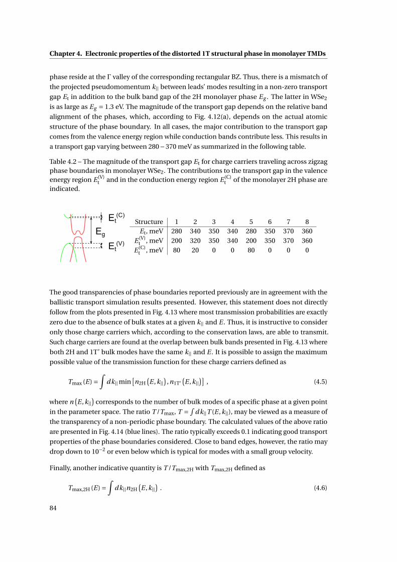
Chapter 4. Electronic properties of the distorted 1T structural phase in monolayer TMDs
phase reside at the Γ valley of the corresponding rectangular BZ. Thus, there is a mismatch of
the projected pseudomomentum k|| between leads’ modes resulting in a non-zero transport
gap Et in addition to the bulk band gap of the 2H monolayer phase Eg . The latter in WSe2
is as large as Eg = 1.3 eV. The magnitude of the transport gap depends on the relative band
alignment of the phases, which, according to Fig. 4.12(a), depends on the actual atomic
structure of the phase boundary. In all cases, the major contribution to the transport gap
comes from the valence energy region while conduction bands contribute less. This results in
a transport gap varying between 280−370 meV as summarized in the following table.
Table 4.2 – The magnitude of the transport gap Et for charge carriers traveling across zigzagphase boundaries in monolayer WSe2. The contributions to the transport gap in the valenceenergy region E (V)
t and in the conduction energy region E (C)t of the monolayer 2H phase are
indicated.
Structure 1 2 3 4 5 6 7 8Et, meV 280 340 350 340 280 350 370 360
E (V)t , meV 200 320 350 340 200 350 370 360
E (C)t , meV 80 20 0 0 80 0 0 0
The good transparencies of phase boundaries reported previously are in agreement with the
ballistic transport simulation results presented. However, this statement does not directly
follow from the plots presented in Fig. 4.13 where most transmission probabilities are exactly
zero due to the absence of bulk states at a given k|| and E . Thus, it is instructive to consider
only those charge carriers which, according to the conservation laws, are able to transmit.
Such charge carriers are found at the overlap between bulk bands presented in Fig. 4.13 where
both 2H and 1T’ bulk modes have the same k|| and E . It is possible to assign the maximum
possible value of the transmission function for these charge carriers defined as
Tmax (E) =∫
dk|| min[n2H
(E ,k||
),n1T′
(E ,k||
)], (4.5)
where n(E ,k||
)corresponds to the number of bulk modes of a specific phase at a given point
in the parameter space. The ratio T /Tmax, T = ∫dk||T (E ,k||), may be viewed as a measure of
the transparency of a non-periodic phase boundary. The calculated values of the above ratio
are presented in Fig. 4.14 (blue lines). The ratio typically exceeds 0.1 indicating good transport
properties of the phase boundaries considered. Close to band edges, however, the ratio may
drop down to 10−2 or even below which is typical for modes with a small group velocity.
Finally, another indicative quantity is T /Tmax,2H with Tmax,2H defined as
Tmax,2H (E) =∫
dk||n2H(E ,k||
). (4.6)
84

4.3. Electronic properties of structural phase boundaries in monolayer WSe2
0.8
1.0
Tmax = 1
1
-1.0
-0.8
E (e
V)
Tmax = 1
0.8
1.0
Tmax = 1
5
-1.0
-0.8
E (e
V)
Tmax = 1
Tmax = 1
2
Tmax = 0. 1
Tmax = 10 2
6
Tmax = 1
0.8
1.0
Tmax = 1
3
-1.0
-0.8
E (e
V)
Tmax = 1
0.8
1.0
Tmax = 10 2
7
Y K K' Y-1.0
-0.8
E (e
V)
Tmax = 1
Tmax = 1
4
Tmax = 0. 1
Tmax = 10 2
8
Y K K' Y
Tmax = 1
0
Tmax
Figure 4.13 – Charge carrier transmission function of the 2H-1T’ phase boundaries in mono-layer WSe2 displayed in Fig. 4.11. The color indicates the value of transmission normalizedby the corresponding maximum indicated in each subplot. The contours of bulk 2H and 1T’monolayer phase bands are shown in each plot.
It is proportional to a maximum possible conductance in the 2H monolayer phase in the
ballistic transport regime. Thus, the above ratio can be used to compare different materials
in terms of their contact properties to the semiconducting 2H phase. The calculated ratio is
presented in Fig. 4.14 as a function of the energy E using red lines. Obviously, T /Tmax,2H <T /Tmax though both values are of the same magnitude. As a result, T /Tmax,2H is typically
between 10−1 and 10−2, however, it may reach higher values away from the band gap region.
4.3.1 Summary
The zigzag boundaries between monolayer 2H and 1T’ phases of WSe2 were evaluated from
the point of view of structural, electronic and transport properties. The topological character
of the boundary is found be consistent with the number, spin character and energy dispersion
85

Chapter 4. Electronic properties of the distorted 1T structural phase in monolayer TMDs
1
0.1
0.01
T/T r
ef 1
-1 -0.8Energy (eV)
1
0.1
0.01
T/T r
ef 5
0.8 1
2
-1 -0.8Energy (eV)
6
0.8 1
3
-1 -0.8Energy (eV)
7
0.8 1
4
-1 -0.8Energy (eV)
8
0.8 1
Figure 4.14 – Relative transmissions T /Tref of the phase boundaries in WSe2 displayed inFig. 4.11. The blue plots compare the transmission function T to the maximum possibletransmission Tref via the open channels of a particular heterojunction. The red plots comparethe transmission function T to the maximum possible transmission Tref in the 2H phase ofthe monolayer WSe2. The edges of a transport gap are indicated by vertical lines.
of electronic bands at the boundary. The possibility of employing 2H-1T’ phase boundaries
for topologically protected charge carrier transport, however, is unclear since multiple in-gap
states contribute to transport properties inside the bulk band gap of monolayer 1T’-WSe2.
Otherwise the high transparency of boundaries for transverse charge carriers is confirmed by
the transport calculations. The contribution to the transport gap of around 300 meV is found
to be consistent with alignment of bulk bands of both monolayer phases in WSe2.
4.4 Electronic properties of dimerization defects in monolayer 1T’-
WSe2
Several previous sections were dedicated to line defects and domain boundaries in the 2H
phase as well as phase boundaries between the 2H and 1T’ phases of monolayer TMDs. To
complete the family of line defects in monolayer TMDs, the dimerization defects in the 1T’
phase have been studied.
Unlike the line defects considered, the dimerization defects in the monolayer 1T’ phase are
stoichiometric. Stoichiometric defects are characterized by lower formation energies and
higher concentrations under thermodynamic equilibrium. In the context of the previous
discussion, the semimetallic 1T’ phase plays a role of a lateral contact in a semcindocting 2D
device. Thus, the electronic properties of the 1T’ monolayer phase are important. The high
defect concentration may affect the properties of the monolayer 1T’-TMDs. From the point
of view of applications, one would also expect a quasi-amorphous phase of the monolayer
1T’ phase where the concentration of dimerization defects is maximal. Such phase may
demonstrate completely different properties compared to the crystalline monolayer 1T’-TMD.
This gives an additional degree of freedom when engineering a 2D device similar to crystalline
86

4.4. Electronic properties of dimerization defects in monolayer 1T’-WSe2
Figure 4.15 – Atomic structures of 1T’ periodic dimerization defects in monolayer WSe2: topand side views. (1) A dimerization defect along the shortest unit cell dimension (zigzag). (2) Adimerization defect along the longest unit cell dimension (armchair). (3) A 120◦ dimerizationdefect separating domains with different orientations of the monolayer 1T’-WSe2 lattices.
and amorphous silicon currently used in nanoelectronics.
At the time of writing of this thesis, not much information exists on dimerization defects
in the 1T’ phase of monolayer TMDs. A quasi-crystalline phase of a sodium-intercalated
multilayer 1T-MoS2 observed in Ref. [84] provides a hint of how a 1T’ dimerization defect could
look like. In particular, the dimerization defect may join domains with different directions
of the zigzag distortion as shown in Fig. 4.15(3). This case corresponds to approximately
120◦ rotation of corresponding crystallographic directions at both sides of the defect. Other
possibilities include breaking of the zigzag distortion without rotating the lattice as illustrated
in Fig. 4.15(1,2). There, periodic dimerization defects are parallel to the shortest or to the
longest vector of a monolayer 1T’-TMD unit cell. All defects keep the underlying monolayer
1T phase intact, thus, the relaxed structures presented in Fig. 4.15 experience only slight
structural distortions at the defect. For consistency with the previous section, the discussion
further is constrained to monolayer 1T’-WSe2 only.
The “zigzag” dimerization defect illustrated in Fig. 4.15(1) originates from a single unpaired
line of tungsten atoms. The relaxed structure, however, prefers to form a triple metallic chain
by merging the single and the bulk-like double chains. Thus, tungsten atoms in the middle
become over-coordinated. The corresponding distance between tungsten atoms 3.04 Å slightly
exceeds the corresponding bulk value of 2.81 Å but is still much smaller than the off-chain
W-W distance in the bulk 4.05 Å.
The “armchair” dimerization defect illustrated in Fig. 4.15(2) breaks metallic chains and rejoins
them in a zip-like manner. As introduced, the periodicity vector for the line defect is bigger in
this case: it is equal to the largest dimension of the unit cell. Both zigzag and armchair defects
87
Chapter 4. Electronic properties of the distorted 1T structural phase in monolayer TMDs
Table 4.3 – Formation energies of dimerization defects in monolayer 1T’-WSe2. The ener-gies are given per unit length. Formation energies of chemically balanced zigzag edges ofmonolayer 1T’-WSe2 from Fig. 4.8 are given for comparison purposes.
Zigzag defect (1) Armchair defect (2) 120◦ defect (3) Edge 1 Edge 2Eform, meV/Å 265 131 58 286 200
connect domains of monolayer 1T’-WSe2 with the same crystallographic orientation. Thus,
they can be avoided by a parallel shift of atoms at one side of the defect. It is not the case for
the 120◦ dimerization defect, Fig. 4.15(3). Unlike the previous defects, it does not possess an
inversion symmetry at the defect line: it joins two 2D crystals rotated with respect to each
other by approximately 120◦. As such, the directions of dimerizations in the two crystals are
different in this case and require a rotation in real space to match.
The dimerization defects considered differ significantly in terms of their formation energies,
Eform in Table 4.3. The most preferred defect is the 120◦ dimerization defect with the for-
mation energy as low as 58 meV per angstrom. The armchair defect is more than two times
expensive in energy while the zigzag defect requires four times more energy to form. This
observation has two important consequences. First, the relatively low formation energy of the
120◦ dimerization defect may cause its high concentrations in real samples as argued in the
beginning of this section. Second, the breaking of the zigzag dimerization of metallic atoms
in the zigzag defect as well as in certain zigzag edges, Fig. 4.8(a), requires significantly more
energy. Compared to chemically-balanced zigzag terminations, the dimerization defects break
less chemical bonds, thus, are expectedly lower in their formation energies3.
All three periodic dimerization defects considered result in different 1D defect Brillouin zones
both in terms of its size and orientation with respect to the leads. The largest BZ is for the
zigzag defect while the smallest one is for the 120◦ dimerization defect. The high-symmetry
points Γ, X, Y of the monolayer 1T’ phase BZ are projected differently as indicated in respective
panels in Fig. 4.16(a). There, either Γ and X or Γ and Y or X and Y are projected onto the same
point of the 1D BZ. This fact prevents the direct comparison of electronic structure properties
of the three defects.
Among the three dimerization defects, only the zigzag dimerization defect shows a clear
presence of localized gapless modes shown in Fig. 4.16(a,1). In contrast, the dimerization
defect along the armchair edge does not cause closing of the small band gap. In both cases,
all localized states are spin-degenerate due to the presence of time-reversal and inversion
symmetries. The 120◦ dimerization defect is different from this perspective: the states localized
at the defect have a pronounced spin character as shown in the inset in Fig. 4.16(a,3). It is
possible because of the lack of an inversion symmetry in the atomic structure. The band gap
is closed or less than the imaginary part of the energy used in Green’s function calculations, 5
3While the formation energy of the edge presented in Table 4.3 belongs to a single monolayer bulk phase of a 1T’TMD, the formation energies of dimerization defects are “split” between the two grains connected by the defect.
88

4.4. Electronic properties of dimerization defects in monolayer 1T’-WSe2
Y ,X Y-1
0
1E
(eV)
1a
X ,Y X
2
X,Y X,Y
3
0.40
0.25
k-resolved DOS
Y , X Y-1
0
1
E (e
V)
1b
X , Y X
2
X, Y X, Y
3
0
3Transmission
Figure 4.16 – Electronic structure properties of dimerization defects in monolayer 1T’-WSe2
from Fig. 4.15. (a) The k-resolved density of electronic states. The blue and red colors on thethird panel indicate the spin-up and spin-down character, respectively, of the density for thenon-inversion-symmetric grain boundary. The inset shows density of states in the vicinity ofthe band gap. (b) The k-resolved charge carrier transmission functions T for charge carrierstraveling across dimerization defects. The color indicates the value of transmission. The bulkbands plotted along high-symmetry directions are shown for the first defect.
meV in this case.
The calculated transmission functions for transverse charge carriers indicate a high trans-
parency of all three defects, Fig. 4.16(b). This can be attributed to the fact that all 3 defects
preserve the lattice structure and stoichiometry to a large extent. Moreover, unlike the mono-
layer 2H phase, the 1T’ phase is non-polar and has a much smaller band gap, thus, the small
charges accumulated at the defects are screened effectively. This reduces the effects of an
electrostatic repulsion in the charge carrier transport. While, looking at Fig. 4.16(b), the trans-
mission across the first defect is subjectively smaller, it effectively corresponds to the smallest
period among all three defects. Thus, the pseudomomentum conservation law for this defect
is pronounced most: there is a large region in the (k||,E) space bounded by the band edges
(red lines in the figure) where no bulk modes are present and no charge carriers transmit.
4.4.1 Summary
The structure, electronic and charge carrier transport properties of simplest stoichiometric
dimerization defects in the 1T’ phase of monolayer WSe2 were investigated. The relaxed
structures of dimerization defects exhibit only moderate structural reconstruction such as the
formation of a triple line of metallic atoms at the line defect along the shortest lattice vector.
89

Chapter 4. Electronic properties of the distorted 1T structural phase in monolayer TMDs
Otherwise local environments of atoms at the defects do not change. Nevertheless, a clear
presence of localized modes at the zigzag defect was observed. In the case of an armchair
defect, however, the modes do not close the band gap in the material. The absence of an
inversion symmetry for the 120◦ dimerization defect lifts the spin degeneracy and causes
localized modes to be spin-polarized. The charge carriers, both holes and electrons, exhibit
high transmission probabilities across all defects considered. It is attributed to the fact that
the monolayer 1T’ phase is non-polar and has a small band gap causing additional charges
accumulated at defects to be screened effectively.
4.5 Conclusions
The 1T’ phase of monolayer TMDs attracts interest from various perspectives. On the one
hand, being semimetallic, it complements the semiconducting 2H phase with applications in
lateral 2D devices. On the other hand, it is a topologically non-trivial phase in the QSH regime
with applications in spintronics and quantum computing. The studied sensitivity of the band
gap and the band order in the 1T’ phase to strain provides a way to both maximize the band
gap and to close it, depending on application requirements. For gapped systems, the QSH
phase was confirmed by studying edges of monolayer 1T’-TMDs. The spin-polarized edge
modes were also confirmed for semimetallic tellurides as well as WS2 which was previously
considered to be a semiconductor. Specific edges of the monolayer 1T’ phase were suggested
for protected transport experiment making TMDs to be the first realistic QSH insulator.
The study of structural and electronic transport properties of phase boundaries between the
2H and 1T’ monolayer phases as well as line defects in the 1T’ phase complements the study
of line defects in the 2H semiconducting materials presented in the previous chapter. The
transparency of 2H-1T’ boundaries for transverse ballistic charge carriers is affected by the
transport gap caused by the difference between shapes of bands of the two phases. Both phase
boundaries and line defects in the monolayer 1T’ phase are transparent for charge carriers
though the relative alignment of bands of the two phases does play a role in the transport
process. The good transparency of defects is in agreement with previous experimental studies
and the fact that the charges in narrow-band-gap materials are screened effectively.
90

5 Simulating STM images of point de-fects in spin-orbit systems
Scanning probe microscopies such as scanning tunneling microscopy (STM) provide an
important insight into the surface structure and properties at the atomistic-scale level. As
described in one of previous sections, such level of spatial resolution is possible with the
help of an atomically sharp tip scanning the material and measuring tunneling conductance.
As a result, a topographic image is recovered where individual atoms and molecules can be
recognized.
An image generated by STM may still be a challenge to interpret due to the fact that a rather
complicated process of electron tunneling is involved in its generation. For example, the
same surface defect may have a qualitatively different contrast in images taken under different
conditions of the STM setup. However, by combining different experimental and theoretical
techniques it becomes possible to identify the defect atomic structure and its electronic
properties.
This chapter describes results of research performed in a close collaboration with experimental
groups towards identifying point defects in two systems: a surface of a Bi2Te3 topological
insulator and a monolayer 2H-MoSe2.
5.1 Magnetic adatoms on the surface of Bi2Te3
As discussed in previous chapters, 3D TIs, such as Bi2Te3, host topologically protected metallic
states on the surface. However, if the time reversal symmetry is broken, the topological
protection is lifted and the electronic band gap on the surface may be opened[98]. One of the
ways to break the time-reversal symmetry is to introduce local magnetic moments. This can
be done by depositing magnetic adatoms, such as Fe, on the surface of a 3D TI. The properties
of such dopants motivated the joint research presented in Ref. [99] where I contributed the
structural identification of dopants and calculations of their magnetic properties.
Two kinds of dopants were identified in the STM experiment. The dopants were observed
as triangular and trefoil-shaped features, see Fig. 5.1. The underlying sublattice formed
91

Chapter 5. Simulating STM images of point defects in spin-orbit systems
26
Fe
experimentH3
T4
FeBi
52
Te83
Bi
xy
xz
xy
xy
xz
xz
simulation
Figure 5.1 – Fe dopants on the surface of Bi2Te3 in 3 possible configurations: H3 (Fe above Te),T4 (Fe above Bi) and FeBi (Fe substituting topmost Bi). The relaxed structures are presentedon the left. The simulated STM images together with corresponding STM images observedin experiment are presented on the right. The STM bias voltage from experiment −0.4 Vcorresponds to the simulated local density of hole-like states. White scale bars are 1 nm.
by the topmost Te atoms is also visible in the experimental images. This allows assigning
dopants to different high-symmetry positions of the lattice: H3 (on top of the tellurium atom
in the third topmost layer) and T4 (on top of the bismuth atom in the second topmost layer).
To identify which high-symmetry position corresponds to which STM image the electronic
structure calculations and simulations of STM images have been performed. By comparing
experimental and simulated images in Fig. 5.1 it is possible to assign the atomic structure of
the H3 adatom to the trefoil-shaped signal and the one of the T4 structure to the triangular-
shaped signal. As expected, the iron atom in the H3 configuration relaxes deeper into the
surface of Bi2Te3, thus, producing a less intense signal in the STM image. In contrast, the
second topmost layer of Bi atoms in the T4 configuration prevents further depression of Fe
into the material resulting in a bright spot in the image. To verify that the Fe adatom in the T4
configuration does not replace the underlying Bi we also performed simulations with the latter
removed from the atomic structure. The resulting STM image, bottom row of Fig. 5.1, shows a
very weak signal from the impurity which was not identified in the original experimental data.
92

5.1. Magnetic adatoms on the surface of Bi2Te3
5.1.1 Thermodynamical properties of adatoms
The adatoms deposited in the experiment were found to be immobile at cryogenic tempera-
tures of T = 10 K. The concentration of Fe adatoms in the H3 atomic configuration, however,
was found to be slightly larger. As reported in Ref. [99], the ratio between concentrations
ρH3/ρT4 ≈ 3/2. These two facts suggest that the H3 configuration is thermodynamically more
stable than the T4 configuration, while the potential barrier between the configurations is too
large for thermally-activated transition between them.
To verify this hypothesis the total energy profile between the H3 and the T4 configurations
was plotted using the nudged elastic band (NEB) method[100]. The calculation details are
given in Appendix A.8. The resulting potential profile shown in Fig. 5.2(a) implies that the
H3 configuration to be more energetically favorable. Depending on the inclusion of the
on-site Coulomb repulsion term for the d-states of Fe[101] U = 3 eV, the energy difference
between the configurations is 0.25 eV (without) or 0.37 eV (with the Coulomb repulsion).
The energy barrier separating configurations is around 1 eV. The barrier is too high for the
thermal diffusion at T = 10K, thus, under experimental conditions the Fe atoms are immobile.
The relative concentrations of the impurities are rather defined by the kinetic aspect of the
deposition process and, in principle, are not related directly to the relative energies of the two
configurations.
5.1.2 Electronic and magnetic properties of adatoms
As mentioned earlier, magnetic impurities may open a band gap1 in the surface Dirac cone
via exchange interaction with helical surface states[98, 35, 37] depending on the direction of
the magnetic moment. The electronic structure results of the STS experiment did not show
any evidence of coupling of helical spins and magnetic moments of Fe adatoms. On the other
hand, the x-ray absorption spectroscopy and x-ray magnetic circular dichroism experiment
results[99] show an out-of-plane magnetic anisotropy of Fe adatoms which, in principle, is
expected to open the band gap in the Dirac cone. To provide an additional insight into the
electronic propertie of Fe adatoms on the surface of Bi2Te3 ab-initio DFT simulations were
carried out.
The electronic band structures calculated for both H3 and T4 atomic configurations and
presented in Fig. 5.2(c,d) do not allow any definitive conclusions with regard to the band gap
since the Dirac cone at the Γ point is buried in a multitude of metallic states due to impurity.
This is due to a relatively small 2x2 supercell employed in the calculations: the Fe adatom
interacts with its images resulting in dispersive bands with a high weight of Fe orbitals shown
in Fig. 5.2(c,d). Similarly, the densities of electronic states plotted in Fig. 5.2(b) do not exhibit
any sharp peaks either.
To understand the magnetic properties of adatoms several DFT simulations were performed.
1Provided the Fermi level is at the Dirac cone touching point
93
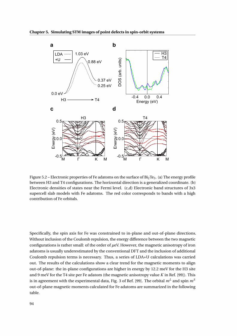
Chapter 5. Simulating STM images of point defects in spin-orbit systems
Figure 5.2 – Electronic properties of Fe adatoms on the surface of Bi2Te3. (a) The energy profilebetween H3 and T4 configurations. The horizontal direction is a generalized coordinate. (b)Electronic densities of states near the Fermi level. (c,d) Electronic band structures of 3x3supercell slab models with Fe adatoms. The red color corresponds to bands with a highcontribution of Fe orbitals.
Specifically, the spin axis for Fe was constrained to in-plane and out-of-plane directions.
Without inclusion of the Coulomb repulsion, the energy difference between the two magnetic
configurations is rather small: of the order of µeV. However, the magnetic anisotropy of iron
adatoms is usually underestimated by the conventional DFT and the inclusion of additional
Coulomb repulsion terms is necessary. Thus, a series of LDA+U calculations was carried
out. The results of the calculations show a clear trend for the magnetic moments to align
out-of-plane: the in-plane configurations are higher in energy by 12.2 meV for the H3 site
and 9 meV for the T4 site per Fe adatom (the magnetic anisotropy value K in Ref. [99]). This
is in agreement with the experimental data, Fig. 3 of Ref. [99]. The orbital mL and spin mS
out-of-plane magnetic moments calculated for Fe adatoms are summarized in the following
table.
94

5.2. Selenium vacancies in monolayer 2H-MoSe2
Table 5.1 – Magnetic properties of Fe adatoms on the surface of Bi2Te3: magnetic momentsand anisotropies calculated by projecting occupied Bloch states onto atomic orbitals.
mS (µBohr) mL (µBohr) K (meV)H3 2.7 0.7 12.2T4 2.5 0.3 9
5.1.3 Conclusions
Results of our theoretical simulations of Fe impurities on the surface of Bi2Te3 are well in
line with experiments. Simulations of STM images allowed us to assign unambiguously H3
and T4 atomic configurations of Fe adatoms to the corresponding experimental results. As
confirmed by the NEB method, the large energy barrier separating two configurations allows
simultaneous observation of both kinds of impurities at experimental conditions. While
there is no conclusive agreement on electronic properties of Fe adatoms, their magnetic
properties are in a good agreement between theory and experiment. The calculated orbital
and spin magnetic moments suggest that Fe adatoms are in a high-spin state. The out-of-
plane magnetic anisotropy of Fe observed in this work is also in agreement with previous
predictions[102, 103] and observations[104].
5.2 Selenium vacancies in monolayer 2H-MoSe2
As discussed in previous chapters, 2D materials are susceptible to various structural defects in-
cluding line and point defects. Our experimental colleagues from Lawrence Berkeley National
Laboratory observed several kinds of point defects in MoSe2 with STM signal changing both
qualitatively and quantitatively as a function of the voltage applied to the STM tip. Surprisingly,
the defects did not show any sign of in-gap states in STS measurements. In contrast, all defects
in a sister material MoS2 are predicted to have in-gap states[105]. We attempted to perform a
similar study for monolayer 2H-MoSe2: to identify the defects and to calculate their electronic
properties.
For 2D MoS2, the most expected point defect predicted[105] is the sulfur vacancy VS. Ac-
cordingly, the selenium vacancy VSe is the most expected point defect in MoSe2. Provided
the stoichiometric balance between molybdenum and selenium atoms is shifted towards
selenium-deficient conditions, one may also expect a defect configuration of a molybdenum
atom substituting one MoSe or two Mo2Se selenium atoms. I performed electronic structure
calculations of the above defects in a supercell geometry (computational details are given in
Appendix A.9) with results presented in Fig. 5.3.
As expected, all defects induce in-gap states localized at the defect, last column in Fig. 5.3.
The defects induce several empty and occupied states in the band gap energy region as
demonstrated in the corresponding DOS plots in Fig. 5.3. The simulated STM images also
indicate the presence of defect states in all cases. The largest intensity obtained during
95
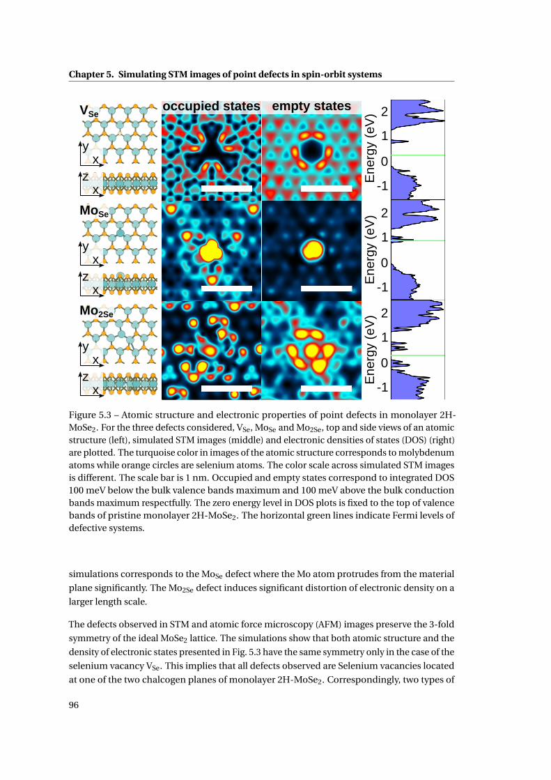
Chapter 5. Simulating STM images of point defects in spin-orbit systems
VSe
MoSe
Mo2Se
occupied states empty states
xy
xz
xy
xy
xz
xz
Ene
rgy
(eV
) 2
1
0
-1
Ene
rgy
(eV
) 2
1
0
-1
Ene
rgy
(eV
) 2
1
0
-1
Figure 5.3 – Atomic structure and electronic properties of point defects in monolayer 2H-MoSe2. For the three defects considered, VSe, MoSe and Mo2Se, top and side views of an atomicstructure (left), simulated STM images (middle) and electronic densities of states (DOS) (right)are plotted. The turquoise color in images of the atomic structure corresponds to molybdenumatoms while orange circles are selenium atoms. The color scale across simulated STM imagesis different. The scale bar is 1 nm. Occupied and empty states correspond to integrated DOS100 meV below the bulk valence bands maximum and 100 meV above the bulk conductionbands maximum respectfully. The zero energy level in DOS plots is fixed to the top of valencebands of pristine monolayer 2H-MoSe2. The horizontal green lines indicate Fermi levels ofdefective systems.
simulations corresponds to the MoSe defect where the Mo atom protrudes from the material
plane significantly. The Mo2Se defect induces significant distortion of electronic density on a
larger length scale.
The defects observed in STM and atomic force microscopy (AFM) images preserve the 3-fold
symmetry of the ideal MoSe2 lattice. The simulations show that both atomic structure and the
density of electronic states presented in Fig. 5.3 have the same symmetry only in the case of the
selenium vacancy VSe. This implies that all defects observed are Selenium vacancies located
at one of the two chalcogen planes of monolayer 2H-MoSe2. Correspondingly, two types of
96
5.2. Selenium vacancies in monolayer 2H-MoSe2
intensity signatures corresponding to the VSe defect are visible in STM: one corresponds to
the vacancy just below the STM tip (the vacancy side) and the other one corresponds to the
vacancy below the material plane (the back side).
5.2.1 Electronic properties of Se vacancies
To further understand electronic properties of Se vacancies in MoSe2 additional electronic
structure simulations were performed. Motivated by the STS data showing no in-gap states
of the defect, the specific focus was made on defect electronic states. As shown in Fig. 5.3,
a single selenium vacancy hosts localized electronic levels close to the edge of conduction
band. For the charge-neutral system these states remain unoccupied. Upon adding electrons
to the system these states start getting populated and the Fermi level of the system moves
up in energy. To understand, whether this is the only effect on the electronic band structure,
additional simulations were carried out.
To simulate a charged selenium vacancy two additional models were considered. The first
model, VSe +e, included an additional electron explicitly such that the total charge of the
supercell model was equal to the electron charge −e. The second model, HSe, realized another
possibility of a hydrogen adatom absorbed by the defect. The latter donates an electron to
the defect, thus, only minor change in electronic properties compared to the VSe +e case is
expected. Both models were relaxed prior to calculating the density of states.
The calculated densities of electronic states presented in Fig. 5.4 show that the localized
states are still present in the band gap energy region in all cases considered. As expected, the
Fermi level shifts towards the conduction band. In the case of a hydrogen adatom, the spin
degeneracy of states is lifted and the total magnetic moment of the model is equal to µBohr.
Four separate peaks corresponding to localized states at the defect are visible in Fig. 5.5. In
either case, charging of defects does not explain the absence of in-gap states in experiment.
There is a good agreement between experimental and simulated STM images in Fig. 5.5. All
vacancy-side images, experimental and simulated, exhibit a contrast depression correspond-
ing to the defect center. The contrast peaks have the same symmetry when comparing the
simulated and the experimental images. The agreement between the images corresponding
to the back side of the defect, however, is not uniform. Specifically, the simulated signal
depressions and peaks corresponding to the positive bias (empty states) are quite similar to
those obtained in experiment. Instead, the images obtained at the negative tip bias (occupied
states) disagree both in terms of location of signal peaks and their symmetry.
5.2.2 Conclusions
Though the results of experiments and theoretical simulations do not agree in terms of the
presence of in-gap states, they do provide an insight into electronic properties of Se vacan-
cies in MoSe2. The Se vacancy can be identified unambigously via the three-fold symmetry
97

Chapter 5. Simulating STM images of point defects in spin-orbit systems
1 0 1 2Energy (eV)
DO
S, a
.u.
MoSe2
VSe
HSe
VSe + e
Figure 5.4 – Density of electronic states for the selenium vacancy defect in monolayer 2H-MoSe2. The four plots correspond to pristine monolayer 2H-MoSe2, the selenium vacancymodel VSe, the hydrogenated selenium vacancy HSe and the negatively charged vacancy VSe +ein a non-magnetic configuration. The Fermi level is indicated in each case.
preserved by the defect. The DFT predicts in-gap localized defect states regardless of defect
kind and its charge state. However, no clue of localized in-gap states was observed in the
experiment. One of the reasons for such behavior may be low tunneling rates between the
defect state and bulk valence bands as explained in Ref. [106]: the charge carriers may prefer
to tunnel directly into the bulk states while the charge carriers localized at the defect are,
effectively, immobile. Further experiments as well as charge carrier tunneling simulations
may provide additional understanding of the effect.
98
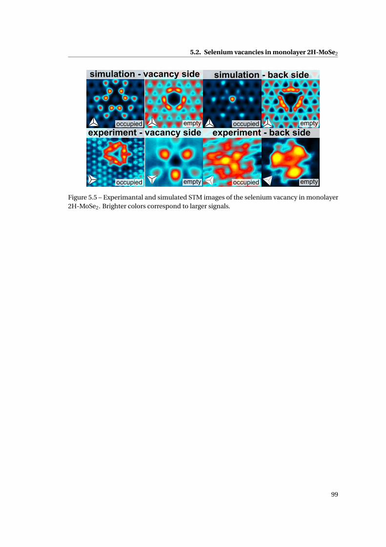
5.2. Selenium vacancies in monolayer 2H-MoSe2
Figure 5.5 – Experimantal and simulated STM images of the selenium vacancy in monolayer2H-MoSe2. Brighter colors correspond to larger signals.
99

6 Outlook
Though the 2D materials remain “hot” topic in a modern materials science, the attention
to the first monolayer material, graphene, seems to saturate. From this perspective, the
recently-discovered family of monolayer materials with a large enough band gap is a promis-
ing discovery with applications in the nanoscale electronics. The relatively short history of
monolayer transition metal dichalcogenides (TMDs) partially resembles the one of graphene
with a particular research focus on the most important properties for applications in electron-
ics: structure, defects, transport properties. However, there are also structural, optical and spin
phenomena which have not been observed in any other material making monolayer TMDs
unique. Among such phenomena is the role of electron spin and the spin-orbit coupling in
materials’ electronic and transport properties.
Each of the spin phenomena considered in the present study is related to a particular applica-
tion, namely, the spin-valley coupling in monolayer 2H-TMDs provides a way to convert the
charge carrier valley into its spin. The transport gap may be exploited in the engineering of
a lateral semiconducting logic device where the domain boundaries either allow or prohibit
charge carrier transport depending on symmetries of a line defect. The spin filtering of charge
carriers is useful for spintronics: as demonstrated, the line defects in monolayer 2H-MoS2 can
be used to generate spin-polarized currents in a non-magnetic media by all-electric means.
Thus, from the experimental perspective, it is of a primary importance to achieve high-quality
material samples suitable for ballistic transport devices. On the theoretical side, the study of
charge carrier scattering mechanisms in monolayer TMDs is required for a better understand-
ing of the diffusive transport in these materials. In particular, the conservation laws being
in the core of the phenomena studied (spin polarization of current, transport gap) have to
be adjusted to the diffusive transport regime accessible experimentally. The methodologi-
cal part could be extended towards a better description of ballistic transport properties in
semiconducting materials. The existing density functional theory non-equilibrium Green’s
function technique has to be extended towards a better description of transport properties of
materials with a band gap. Specifically, the charge accumulation at the defect, the treatment
of long-range electrostatic potentials and the incorrect band alignment of materials in contact
101

Chapter 6. Outlook
are known issues to overcome.
Another very popular topic in solid-state physics, the topology of electronic states, was also
discussed in the thesis on the example of a metastable structural 1T’ phase of monolayer
TMDs. The electronic properties of the quantum spin Hall phase as well as the transport
properties of phase boundaries presented are well in line with the experimental results. The
study can be extended in several ways. First, the line defects presented are rather a “good guess”
of what can be observed in experiment. Consecutively, a more complete study of possible
line defects should be performed with a particular accent on the comparison with the future
experiments. Second, the existence and the magnitude of the small band gap in monolayer
1T’-TMDs remains an open question. While a number of DFT, GW and hybrid functional
studies of the monolayer 1T’ phase are published, still no agreement is available. One of the
possible sources of the disagreement was discussed in the thesis, namely, the sensitiveness
of the band gap magnitude to the lattice constants. Further investigations, including the
investigation of many-body effects in the electronic properties of monolayer 1T’-TMDs, are
yet to be done.
102

A Appendix
A.1 On left and right eigenvalues
For a Hermitian matrix H = H† the left and right eigenstates are simply connected via a
Hermitian conjugation
Hψ= Eψ ⇒ ψ†H =ψ†E∗ . (A.1)
This gives a well-known fact that a Hermitian matrix has real eigenvalues
E =ψ†Eψ=ψ†(Eψ) =ψ†(Hψ) = (ψ†H)ψ=ψ†E∗ψ= E∗ . (A.2)
As a consequence of the above, the eigenvalues of left eigenstates E∗ are the same as eigenval-
ues of right eigenstates E .
The above proof does not hold for non-Hermitian matrices A 6= A†. As a result, the left and
right eigenstates of non-Hermitian matrices are different. Does this also mean that “left” and
“right” eigenvalues are different as well? The answer is no, however, it is impossible to show it
in a matrix-only way: a determinant property is used. Specifically,
Aψ=λψ⇔ (A−λ)ψ= 0 ⇔ det(A−λ) = 0 . (A.3)
Left equation similarly leads to
ψA =ψλ⇔ψ(A−λ) = 0 ⇔ det([A−λ]T)= 0 . (A.4)
The determinant of a matrix and the one of its transpose are exactly equivalent, thus, the
above polynomial equations are exactly the same. Their roots are the same as well, thus, the
sets of left eigenvalues and right eigenvalues are equal. Importantly, this holds for an arbitrary
kind of an eigenvalue equations
F(λ)ψ= 0, ψF(λ) = 0 (A.5)
103

Appendix A. Appendix
including generalized eigenvalue problem
Aψ=λBψ⇔ F =λB−A (A.6)
and higher-order eigenvalue equations
Aψ+λBψ+λ2Cψ= 0 ⇔ F = A+λB+λ2C . (A.7)
For this reason there is no need in “left” and “right” eigenvalues: they are the same.
A.2 Valley filtering with line defects
In the original work[73] of Daniel Gunlycke and Carter White the valley-polarized charge carrier
transport across a line defect in graphene was predicted. Since the idea of spin-polarized
transport in TMDs is based on similar concepts I will briefly review the results of their study.
Consider a mirror-symmetric line defect in graphene such as the one in Fig A.1. How does the
symmetry affect the eigenstates in this system? To answer this question the authors propose
to split the entire lattice into two sublattices colored by blue and gray1 in Fig. A.1. There are
two possible ways to do it as illustrated on the left-hand side and on the right-hand side of the
figure. Because of the mirror symmetry, however, these color schemes are equivalent. Thus,
an operator cross-mapping the sublattices in graphene commutes with the single-particle
Hamiltonian of the entire system. Such operator is presented by the Pauli matrix σx coupling
sublattices A and B in the original study. For more complete description it is possible introduce
the following operator
M =
0 1 0
1 0 0
0 0 1
, (A.8)
where M1,2 = M2,1 = 1 cross-maps blue A and gray B sublattices and M3,3 = 1 maps graphene
atoms M in the middle (black in Fig. A.1) onto themselves. By above symmetry arguments,
this operator commutes with the Hamiltonian. Thus, both can be diagonalized with the same
set of eigenstates. There are two families of eigenstates of M corresponding to eigenvalues
m =±1. They can be expressed as
ψm=1 = c1 (|A⟩+ |B⟩)+ c2 |M⟩ , ψm=−1 = 1p2
(|A⟩− |B⟩) , (A.9)
1Note that the coloring is not mirror-symmetric
104
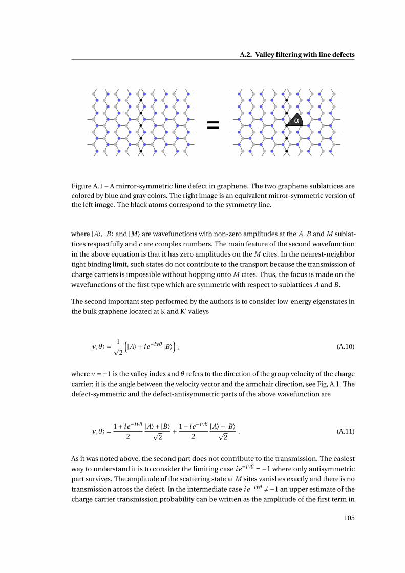
A.2. Valley filtering with line defects
Figure A.1 – A mirror-symmetric line defect in graphene. The two graphene sublattices arecolored by blue and gray colors. The right image is an equivalent mirror-symmetric version ofthe left image. The black atoms correspond to the symmetry line.
where |A⟩, |B⟩ and |M⟩ are wavefunctions with non-zero amplitudes at the A, B and M sublat-
tices respectfully and c are complex numbers. The main feature of the second wavefunction
in the above equation is that it has zero amplitudes on the M cites. In the nearest-neighbor
tight binding limit, such states do not contribute to the transport because the transmission of
charge carriers is impossible without hopping onto M cites. Thus, the focus is made on the
wavefunctions of the first type which are symmetric with respect to sublattices A and B .
The second important step performed by the authors is to consider low-energy eigenstates in
the bulk graphene located at K and K’ valleys
|ν,θ⟩ = 1p2
(|A⟩+ i e−iνθ |B⟩
), (A.10)
where ν=±1 is the valley index and θ refers to the direction of the group velocity of the charge
carrier: it is the angle between the velocity vector and the armchair direction, see Fig, A.1. The
defect-symmetric and the defect-antisymmetric parts of the above wavefunction are
|ν,θ⟩ = 1+ i e−iνθ
2
|A⟩+ |B⟩p2
+ 1− i e−iνθ
2
|A⟩− |B⟩p2
. (A.11)
As it was noted above, the second part does not contribute to the transmission. The easiest
way to understand it is to consider the limiting case i e−iνθ =−1 where only antisymmetric
part survives. The amplitude of the scattering state at M sites vanishes exactly and there is no
transmission across the defect. In the intermediate case i e−iνθ 6= −1 an upper estimate of the
charge carrier transmission probability can be written as the amplitude of the first term in
105
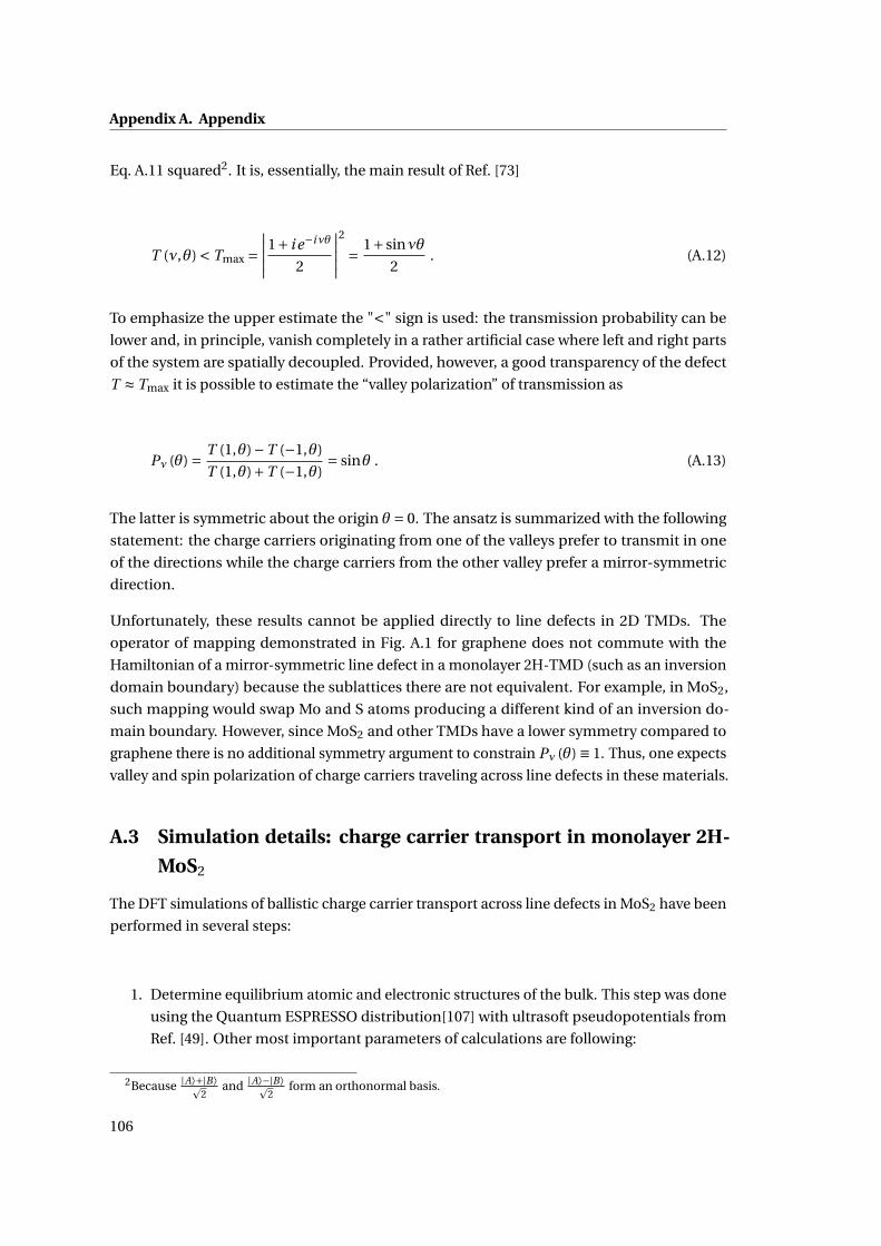
Appendix A. Appendix
Eq. A.11 squared2. It is, essentially, the main result of Ref. [73]
T (ν,θ) < Tmax =∣∣∣∣∣1+ i e−iνθ
2
∣∣∣∣∣2
= 1+ sinνθ
2. (A.12)
To emphasize the upper estimate the "<" sign is used: the transmission probability can be
lower and, in principle, vanish completely in a rather artificial case where left and right parts
of the system are spatially decoupled. Provided, however, a good transparency of the defect
T ≈ Tmax it is possible to estimate the “valley polarization” of transmission as
Pν (θ) = T (1,θ)−T (−1,θ)
T (1,θ)+T (−1,θ)= sinθ . (A.13)
The latter is symmetric about the origin θ = 0. The ansatz is summarized with the following
statement: the charge carriers originating from one of the valleys prefer to transmit in one
of the directions while the charge carriers from the other valley prefer a mirror-symmetric
direction.
Unfortunately, these results cannot be applied directly to line defects in 2D TMDs. The
operator of mapping demonstrated in Fig. A.1 for graphene does not commute with the
Hamiltonian of a mirror-symmetric line defect in a monolayer 2H-TMD (such as an inversion
domain boundary) because the sublattices there are not equivalent. For example, in MoS2,
such mapping would swap Mo and S atoms producing a different kind of an inversion do-
main boundary. However, since MoS2 and other TMDs have a lower symmetry compared to
graphene there is no additional symmetry argument to constrain Pν (θ) ≡ 1. Thus, one expects
valley and spin polarization of charge carriers traveling across line defects in these materials.
A.3 Simulation details: charge carrier transport in monolayer 2H-
MoS2
The DFT simulations of ballistic charge carrier transport across line defects in MoS2 have been
performed in several steps:
1. Determine equilibrium atomic and electronic structures of the bulk. This step was done
using the Quantum ESPRESSO distribution[107] with ultrasoft pseudopotentials from
Ref. [49]. Other most important parameters of calculations are following:
2Because |A⟩+|B⟩p2
and |A⟩−|B⟩p2
form an orthonormal basis.
106

A.4. Simulation details: spin polarization of the transmission probability in monolayer2H-MoS2
wavefunction cutoff 80 Ry
density cutoff 1000 Ry
k grid 18x18
energy convergence criterion 10−6 Ry
force convergence criterion 10−5 RyaBohr
pressure convergence criterion 1 bar
size of the unit cell in the vacuum direction 2 nm
2. Determine the equilibrium atomic structure of the defect. The structural optimization
calculations were done in supercell configurations where the line defects were separated
by at least 1.5 nm in the transport direction, see the atomic structure presentid in Fig. 2.7
for an example.
3. Determine transport properties using NEGF technique. The last step was performed
using the OpenMX code[108]. The size of the unit cell in the vacuum direction was
increased to 10 nm for the correct description of electrostatic effects. The localized basis
set Mo:s2p2d2f1 S:s2p3d1 was found to correctly reproduce the bulk band structure
obtained previously. The scattering regions where deviations from the bulk charge
density and potential are allowed were 3-5 nm large along the transport direction.
The electrostatic potential obtained in the Dirichlet boundary conditions was used to
obtain transport properties including transmission. The leads’ bulk states were perfectly
aligned in energy: the voltage bias was assumed to be zero.
A.4 Simulation details: spin polarization of the transmission prob-
ability in monolayer 2H-MoS2
In 2D systems with a 1D defect, the total transmission function value T defined by the Caroli
expression, Eq. 2.75, is a function of the pseudomomentum projection k||. In Lanauer-Buttiker
formula, Eq. 2.29, this dependence was omitted. To include it, one typically assumes the
contacts to be much larger than the size of the device and takes the transmission function
average
T (E) =0.5∫
k||=−0.5
dk||T (E ,k||) , (A.14)
where k|| is a coordinate in the BZ expressed in reciprocal lattice units.
However, to be able to generate spin-polarized currents using line defects in MoS2 one has to
break the k|| –(−k||
)symmetry because otherwise
Pσ(E) =0.5∫
k||=−0.5
dk||Pσ(E ,k||) = 0 , (A.15)
107

Appendix A. Appendix
where Pσ(E ,k||) is defined in Eq. 3.5. This is done by considering an opposite limiting case
where contacts’ size is much smaller than the distance between them. This allows to force the
ballistic current to propagate along some well-defined direction θ within small angle dθ. The
corresponding Lanauer-Buttiker formula is
d I = dθ · e
h
∫dE ·τ(E ,θ) f ′(E) , (A.16)
where the angle θ is calculated for a given lead mode
θ = arctanv||vtr
= arctan∂E/∂k||∂E/∂ktr
, (A.17)
where E(~k) is a dispersion of the energy band the state belongs to and ktr is a projection of
the pseudomomentum along the transport direction. The τ function resembles the total
transmission for a given angle θ. For consistency, after integrating Eq. A.16 the original current
value should be recovered
I = e
h
∫dθ
∫dE ·τ(E ,θ) f ′(E) . (A.18)
The above expression is very similar to the original Eq. 2.29 with Eq. A.14 substituted
I = e
h
∫dk||
∫dE ·T (E ,k||) f ′(E) . (A.19)
Thus, it should be possible to define τ by corresponding the above two equations using the
Dirac δ-function. The problem, however, is that neither map k|| → θ nor θ→ k|| exist as a
function. Thus, one has to split integration into branches shown as colored arcs in Fig. A.2.
Within each branch, the bulk states can be parametrized by both k|| and, more importantly, θ.
Eqs. A.18, A.19 can be written as
I = e
h
∫dE f ′(E)
∑b∈{branches}
θmaxb∫
θ=θminb
dθ ·τb(E ,θ) (A.20)
and
I = e
h
∫dE f ′(E)
∑b∈{branches}
kmaxb∫
k||=kminb
dk|| ·Tb(E ,k||) . (A.21)
The above equations are satisfied, for example, if
τb(E ,θ) = ∂k||(θ)
∂θTb(E ,k|| (θ)) . (A.22)
By taking the sum over specific branches, see Fig. A.2(c), the angle-dependent transmission is
108
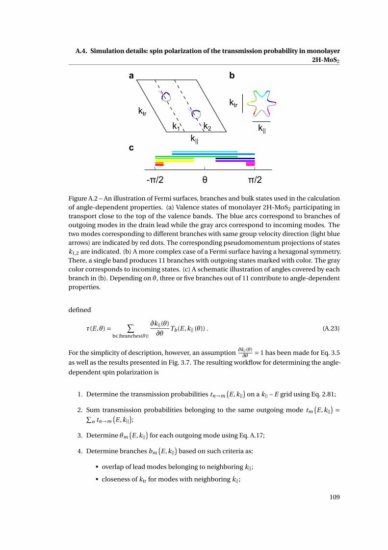
A.4. Simulation details: spin polarization of the transmission probability in monolayer2H-MoS2
Figure A.2 – An illustration of Fermi surfaces, branches and bulk states used in the calculationof angle-dependent properties. (a) Valence states of monolayer 2H-MoS2 participating intransport close to the top of the valence bands. The blue arcs correspond to branches ofoutgoing modes in the drain lead while the gray arcs correspond to incoming modes. Thetwo modes corresponding to different branches with same group velocity direction (light bluearrows) are indicated by red dots. The corresponding pseudomomentum projections of statesk1,2 are indicated. (b) A more complex case of a Fermi surface having a hexagonal symmetry.There, a single band produces 11 branches with outgoing states marked with color. The graycolor corresponds to incoming states. (c) A schematic illustration of angles covered by eachbranch in (b). Depending on θ, three or five branches out of 11 contribute to angle-dependentproperties.
defined
τ(E ,θ) = ∑b∈{branches(θ)}
∂k||(θ)
∂θTb(E ,k|| (θ)) . (A.23)
For the simplicity of description, however, an assumption∂k||(θ)∂θ = 1 has been made for Eq. 3.5
as well as the results presented in Fig. 3.7. The resulting workflow for determining the angle-
dependent spin polarization is
1. Determine the transmission probabilities tn→m(E ,k||
)on a k|| – E grid using Eq. 2.81;
2. Sum transmission probabilities belonging to the same outgoing mode tm(E ,k||
) =∑n tn→m
(E ,k||
);
3. Determine θm(E ,k||
)for each outgoing mode using Eq. A.17;
4. Determine branches bm(E ,k||
)based on such criteria as:
• overlap of lead modes belonging to neighboring k||;
• closeness of ktr for modes with neighboring k||;
109

Appendix A. Appendix
• smoothness and extreme points of function θ(k||
);
This step requires a heuristic analysis on a fine enough grid of k||;
5. Combine above quantities into θb(E ,k||
)and tb (E ,θ). The latter should be interpolated
on a grid of values of θ within an interval[θmin
b ,θmaxb
]. The quantities θmin,max
b are either
extreme points of θ(k||
)or equal to ±π/2;
6. Calculate∂k||(θ)∂θ by inverting function θb
(E ,k||
)or assume the former to be equal to one;
7. Calculate the total transmission using Eq. A.23 as well as the spin transmission using a
modified expression
τσ(E ,θ) = ∑b∈{branches(θ)}
∂k||(θ)
∂θTb(E ,k|| (θ)) ·σb
(E ,k||(θ)
). (A.24)
8. Calculate Pσ(E ,θ) = τσ(E ,θ)/τ(E ,θ).
A.5 Projected3 band structure in monolayer 2H-MoS2 and other 2D
materials
To understand the charge carrier transmission across a periodic line defect one has to consider
the interplay between bulk states of the leads. This is done by projecting the bulk band
structure onto a 1D Brillouin zone of a line defect. In other words one has to map the 2D BZ~K = (kx ,ky ) to the 1D BZ k||. This is closely related to the “folding”4 of the band structure. A
brief mathematical introduction is given further.
Consider a (crystal) basis A such that the Cartesian coordinates ~R are related to the crystal
coordinates~r via the following matrix-vector product
~R = A~r . (A.25)
The matrix A has unit vectors of a crystal as its columns. Similarly, the corresponding reciprocal
basis B having reciprocal unit vectors as its columns connects Cartesian coordinates of a wave
vector ~K and its reciprocal crystal coordinates~k
~K = B~k . (A.26)
The defining relation between the real and the reciprocal basises is the inverse-transpose
operation (an optional 2π factor is omitted)
B = (A−1)T
. (A.27)
3Not to confuse with orbital-projected band structure4The term “folding” rather means producing shifted replicas in the context of the discussion
110

A.5. Projected band structure in MoS2 and other TMDs
Though the basis A contains unit vectors it is possible to define another basis A′ to, for example,
describe a supercell. The general relation between the basis and its alternate version is the
matrix product
A′ = AN , (A.28)
where the square matrix N contains integers similar to Eq. 2.6. The new basis A′ may describe
a unit cell or a supercell, depending on available symmetries and values in N. In either case its
reciprocal counterpart is described by the matrix
B′ =(A′−1
)T. (A.29)
Provided A′ is a supercell basis, the electronic band structure of a material gets “folded” such
that multiple points in the original BZ are projected onto the same point in the new BZ. Lets
find the mapping. Consider ~K = (kx ,ky ) having the same reciprocal Cartesian coordinates in
both basis sets
~K = B~k = B′~k ′ . (A.30)
The new reciprocal lattice coordinates~k ′ are simply
~k ′ = (B′)−1 B~k = A′TB~k = NTATB~k = NT~k . (A.31)
As a relevant example, consider the hexagonal lattice of monolayer 2H-TMDs. The lattice unit
cell can be defined as
A = (~a1,~a2) =[
a a/2
0p
32 a
]. (A.32)
The reciprocal unit cell demonstrated in Fig. 3.1(c) is
B = (A−1)T =
[1/a 0
−1/p
3a 2/p
3a
]. (A.33)
It is easy to identify the crystal coordinates of points K and K’ to be
k (K) =[
1/3
2/3
], k
(K′)= [
2/3
1/3
]. (A.34)
The 1D Brillouin zone of a defect can be obtained in the limit when one of the supercell vectors
approaches infinity. It can be written symbolically for the left lead as
A′ = AN = A
[nL ∞mL ∞
], (A.35)
111
Appendix A. Appendix
where nL , mL are integer coordinates of the defect periodicity vector defined in Eq. 3.1. Using
Eq. A.31 it is deduces that
~k ′ (K) =[
k|| (K)
·
]=
[nL mL
∞ ∞
][1/3
2/3
]=
[nL+2mL
3
·
]. (A.36)
Since the reciprocal lattice is periodic the reciprocal crystal coordinates are defined up to an
arbitrary integer i
{k|| (K)
}= {nL +2mL
3+ i , i ∈ Z
}=
{(nL −mL) mod 3
3+ i , i ∈ Z
}. (A.37)
Similarly,
{k||
(K′)}= {
(mL −nL) mod 3
3+ i , i ∈ Z
}= {−k|| (K)
}. (A.38)
Above equation results in Eq. 3.2 up to a factor π.
Finally, the size of the transport gap is simply deduced by looking at Fig. 3.6. Under the first
approximation, the quasi-free hole charge carriers at K and K’ exhibit the following dispersion
law
E =−ħ2 |δk|22m∗ , (A.39)
where m∗ is the positive effective mass and δk is a small distance to K or K’ in the reciprocal
space. The spin-conserving channels are released either at the edges of a 1D BZ (if neither K,
K’ point is projected onto k|| = 0) or at k|| = 2π6d (if one of the leads has its K,K’ points projected
onto k|| = 0). In either case the corresponding δk = 2π6d which immediately yields expression in
Eq. 3.4.
A.6 Simulation details: periodic zigzag terminations of monolayer
1T’-TMDs
The structures of zigzag terminations were obtained by relaxing inversion-symmetric zigzag
nanoribbons of various widths up to 7 nm using the Quantum ESPRESSO distribution[107]
with non-relativistic ultrasoft pseudopotentials from Ref. [49]. The nanoribbon images were
decoupled by, at least, 1 nm in the material plane and by 2 nm away from it. Other most
important parameters of simulations are following:
wavefunction cutoff 65 Ry
density cutoff 1000 Ry
k points 12
energy convergence criterion 10−6 Ry
force convergence criterion 10−3 RyaBohr
(default)
112

A.7. Local densities of states at the zigzag terminations of monolayer 1T’-TMDs
To calculate local densities of states presented in Fig.4.9 the nanoribbon Hamiltonian was
expressed in the localized basis set by means of the OpenMX code[108]. Afterwards, one of
the equivalent nanoribbon edges was replaced by a semi-infinite bulk material. The resulting
structure was used to obtain the local density of states of the edge using the NEGF technique.
A.7 Local densities of states at the zigzag terminations of monolayer
1T’-TMDs
The local densities of electronic states of all zigzag terminations are presented in Fig. A.3.
A.8 Simulation details: Fe adatoms on the surface of Bi2Te3
The models of Fe adatoms on the surface of Bi2Te3 were relaxed in 2x2 supercells of Bi2Te3
slabs using the Quantum ESPRESSO distribution[107]. The slab contained 3 quintuple layers
of Bi2Te3 resulting in 60 atoms per supercell plus one Fe adatom. Other most important
parameters of simulations are the following
wavefunction cutoff 50 Ry
density cutoff 300 Ry
k grid 2x2
energy convergence criterion 10−4 Ry (default)
force convergence criterion 10−3 RyaBohr
(default)
size of the unit cell in the vacuum direction 2.5 nm
Hubbard U 3 eV
The nudged elastic band calculations were carried out with five images (one “climbing”
image[109]).
A.9 Simulation details: point defects in MoSe2
The models of point defects were relaxed in 5x5 supercells of monolayer 2H-MoSe2 using the
Quantum ESPRESSO distribution[107] with nonrelativistic ultrasoft pseudopotentials from
Ref. [49]. The most important parameters of the simulations are the following
wavefunction cutoff 65 Ry
density cutoff 1000 Ry
k grid 3x3
energy convergence criterion 10−6 Ry
force convergence criterion 10−3 RyaBohr
(default)
size of the unit cell in the vacuum direction 2 nm
The simulated STM images presented in Fig. 5.3 were obtained by integrating the local
113
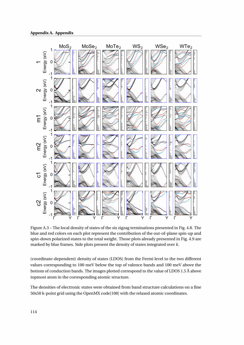
Appendix A. Appendix
-1
0
1En
ergy
(eV)
1MoS2
-1
0
1
Ener
gy (e
V)2
-1
0
1
Ener
gy (e
V)m
1
-1
0
1
Ener
gy (e
V)m
2
-1
0
1
Ener
gy (e
V)c1
Y-1
0
1
Ener
gy (e
V)c2
MoSe2
Y
MoTe2
Y
WS2
Y
WSe2
Y
WTe2
Y
Figure A.3 – The local density of states of the six zigzag terminations presented in Fig. 4.8. Theblue and red colors on each plot represent the contribution of the out-of-plane spin-up andspin-down polarized states to the total weight. Those plots already presented in Fig. 4.9 aremarked by blue frames. Side plots present the density of states integrated over k.
(coordinate-dependent) density of states (LDOS) from the Fermi level to the two different
values corresponding to 100 meV below the top of valence bands and 100 meV above the
bottom of conduction bands. The images plotted correspond to the value of LDOS 1.5 Å above
topmost atom in the corresponding atomic structure.
The densities of electronic states were obtained from band structure calculations on a fine
50x50 k-point grid using the OpenMX code[108] with the relaxed atomic coordinates.
114

Bibliography
[1] Products (Formerly Skylake), 2016.
[2] S. Lebègue and O. Eriksson. Electronic structure of two-dimensional crystals from
\textit{ab initio} theory. Physical Review B, 79(11):115409, March 2009.
[3] Ken Shirriff. Reverse-engineering the TL431: the most common chip you’ve never heard
of, 2014.
[4] J. Bardeen and W. H. Brattain. The Transistor, A Semi-Conductor Triode. Physical Review,
74(2):230–231, July 1948.
[5] Eugen Merzbacher. Quantum Mechanics. Wiley, 3 edition, January 1998.
[6] Paul Benioff. The computer as a physical system: A microscopic quantum mechani-
cal Hamiltonian model of computers as represented by Turing machines. Journal of
Statistical Physics, 22(5):563–591, May 1980.
[7] P. Shor. Polynomial-Time Algorithms for Prime Factorization and Discrete Logarithms
on a Quantum Computer. SIAM Journal on Computing, 26(5):1484–1509, October 1997.
[8] Han Wang, Lili Yu, Yi-Hsien Lee, Yumeng Shi, Allen Hsu, Matthew L. Chin, Lain-Jong
Li, Madan Dubey, Jing Kong, and Tomas Palacios. Integrated Circuits Based on Bilayer
MoS2 Transistors. Nano Letters, 12(9):4674–4680, September 2012.
[9] K. S. Novoselov, D. Jiang, F. Schedin, T. J. Booth, V. V. Khotkevich, S. V. Morozov, and
A. K. Geim. Two-dimensional atomic crystals. Proceedings of the National Academy of
Sciences of the United States of America, 102(30):10451–10453, July 2005.
[10] K. S. Novoselov, A. K. Geim, S. V. Morozov, D. Jiang, Y. Zhang, S. V. Dubonos, I. V. Grig-
orieva, and A. A. Firsov. Electric Field Effect in Atomically Thin Carbon Films. Science,
306(5696):666–669, October 2004.
[11] A. H. Castro Neto, F. Guinea, N. M. R. Peres, K. S. Novoselov, and A. K. Geim. The
electronic properties of graphene. Reviews of Modern Physics, 81(1):109–162, January
2009.
115
Bibliography
[12] Andrea Splendiani, Liang Sun, Yuanbo Zhang, Tianshu Li, Jonghwan Kim, Chi-Yung
Chim, Giulia Galli, and Feng Wang. Emerging Photoluminescence in Monolayer MoS2.
Nano Letters, 10(4):1271–1275, 2010.
[13] Kin Fai Mak, Changgu Lee, James Hone, Jie Shan, and Tony F. Heinz. Atomically Thin
MoS_{2}: A New Direct-Gap Semiconductor. Physical Review Letters, 105(13):136805,
September 2010.
[14] Branimir Radisavljevic, Michael Brian Whitwick, and Andras Kis. Integrated Circuits and
Logic Operations Based on Single-Layer MoS2. ACS Nano, 5(12):9934–9938, December
2011.
[15] B. Radisavljevic, A. Radenovic, J. Brivio, V. Giacometti, and A. Kis. Single-layer MoS2
transistors. Nature Nanotechnology, 6(3):147–150, March 2011.
[16] Di Xiao, Gui-Bin Liu, Wanxiang Feng, Xiaodong Xu, and Wang Yao. Coupled Spin and
Valley Physics in Monolayers of MoS_{2} and Other Group-VI Dichalcogenides. Physical
Review Letters, 108(19):196802, May 2012.
[17] Hualing Zeng, Junfeng Dai, Wang Yao, Di Xiao, and Xiaodong Cui. Valley polarization in
MoS2 monolayers by optical pumping. Nature Nanotechnology, 7(8):490–493, August
2012.
[18] Kin Fai Mak, Keliang He, Jie Shan, and Tony F. Heinz. Control of valley polarization in
monolayer MoS2 by optical helicity. Nature Nanotechnology, 7(8):494–498, August 2012.
[19] Ting Cao, Gang Wang, Wenpeng Han, Huiqi Ye, Chuanrui Zhu, Junren Shi, Qian Niu,
Pingheng Tan, Enge Wang, Baoli Liu, and Ji Feng. Valley-selective circular dichroism of
monolayer molybdenum disulphide. Nature Communications, 3:887, June 2012.
[20] Zhaoqiang Zheng, Tanmei Zhang, Jiandomg Yao, Yi Zhang, Jiarui Xu, and Guowei Yang.
Flexible, transparent and ultra-broadband photodetector based on large-area WSe 2
film for wearable devices. Nanotechnology, 27(22):225501, 2016.
[21] Li Tao, Eugenio Cinquanta, Daniele Chiappe, Carlo Grazianetti, Marco Fanciulli, Madan
Dubey, Alessandro Molle, and Deji Akinwande. Silicene field-effect transistors operating
at room temperature. Nature Nanotechnology, 10(3):227–231, March 2015.
[22] Pere Miró, Martha Audiffred, and Thomas Heine. An atlas of two-dimensional materials.
Chemical Society Reviews, 43(18):6537, May 2014.
[23] C. L. Kane and E. J. Mele. ${Z}_{2}$ Topological Order and the Quantum Spin Hall Effect.
Physical Review Letters, 95(14):146802, September 2005.
[24] B. Andrei Bernevig, Taylor L. Hughes, and Shou-Cheng Zhang. Quantum Spin Hall Effect
and Topological Phase Transition in HgTe Quantum Wells. Science, 314(5806):1757–1761,
December 2006.
116

Bibliography
[25] B. Andrei Bernevig and Shou-Cheng Zhang. Quantum Spin Hall Effect. Physical Review
Letters, 96(10):106802, March 2006.
[26] Markus König, Steffen Wiedmann, Christoph Brüne, Andreas Roth, Hartmut Buhmann,
Laurens W. Molenkamp, Xiao-Liang Qi, and Shou-Cheng Zhang. Quantum Spin Hall
Insulator State in HgTe Quantum Wells. Science, 318(5851):766–770, November 2007.
[27] Liang Fu and C. L. Kane. Topological insulators with inversion symmetry. Physical
Review B, 76(4):045302, July 2007.
[28] Joel Moore. Topological insulators: The next generation. Nature Physics, 5(6):378–380,
June 2009.
[29] M. Z. Hasan and C. L. Kane. Colloquium : Topological insulators. Reviews of Modern
Physics, 82(4):3045–3067, November 2010.
[30] Xiao-Liang Qi and Shou-Cheng Zhang. Topological insulators and superconductors.
Reviews of Modern Physics, 83(4):1057–1110, October 2011.
[31] Alexei Kitaev. Periodic table for topological insulators and superconductors. In AIP
Conference Proceedings, volume 1134, pages 22–30. AIP Publishing, May 2009.
[32] Y. L. Chen, J. G. Analytis, J.-H. Chu, Z. K. Liu, S.-K. Mo, X. L. Qi, H. J. Zhang, D. H. Lu, X. Dai,
Z. Fang, S. C. Zhang, I. R. Fisher, Z. Hussain, and Z.-X. Shen. Experimental Realization
of a Three-Dimensional Topological Insulator, Bi2te3. Science, 325(5937):178–181, July
2009.
[33] Y. Xia, D. Qian, D. Hsieh, L. Wray, A. Pal, H. Lin, A. Bansil, D. Grauer, Y. S. Hor, R. J. Cava,
and M. Z. Hasan. Observation of a large-gap topological-insulator class with a single
Dirac cone on the surface. Nature Physics, 5(6):398–402, June 2009.
[34] Haijun Zhang, Chao-Xing Liu, Xiao-Liang Qi, Xi Dai, Zhong Fang, and Shou-Cheng
Zhang. Topological insulators in Bi2se3, Bi2te3 and Sb2te3 with a single Dirac cone on
the surface. Nature Physics, 5(6):438–442, 2009.
[35] Y. L. Chen, J.-H. Chu, J. G. Analytis, Z. K. Liu, K. Igarashi, H.-H. Kuo, X. L. Qi, S. K. Mo, R. G.
Moore, D. H. Lu, M. Hashimoto, T. Sasagawa, S. C. Zhang, I. R. Fisher, Z. Hussain, and
Z. X. Shen. Massive Dirac Fermion on the Surface of a Magnetically Doped Topological
Insulator. Science, 329(5992):659–662, August 2010.
[36] James G. Analytis, Jiun-Haw Chu, Yulin Chen, Felipe Corredor, Ross D. McDonald,
Z. X. Shen, and Ian R. Fisher. Bulk Fermi surface coexistence with Dirac surface
state in ${\text{Bi}}_{2}{\text{Se}}_{3}$: A comparison of photoemission and Shub-
nikov\char21{}de Haas measurements. Physical Review B, 81(20):205407, May 2010.
[37] L. Andrew Wray, Su-Yang Xu, Yuqi Xia, David Hsieh, Alexei V. Fedorov, Yew San Hor,
Robert J. Cava, Arun Bansil, Hsin Lin, and M. Zahid Hasan. A topological insulator
117

Bibliography
surface under strong Coulomb, magnetic and disorder perturbations. Nature Physics,
7(1):32–37, January 2011.
[38] Oleg V. Yazyev, Joel E. Moore, and Steven G. Louie. Spin Polarization and Transport of
Surface States in the Topological Insulators ${\mathrm{Bi}}_{2}{\mathrm{Se}}_{3}$ and
${\mathrm{Bi}}_{2}{\mathrm{Te}}_{3}$ from First Principles. Physical Review Letters,
105(26):266806, December 2010.
[39] S. B. Zhang and John E. Northrup. Chemical potential dependence of defect formation
energies in GaAs: Application to Ga self-diffusion. Physical Review Letters, 67(17):2339–
2342, October 1991.
[40] Wu Zhou, Xiaolong Zou, Sina Najmaei, Zheng Liu, Yumeng Shi, Jing Kong, Jun Lou,
Pulickel M. Ajayan, Boris I. Yakobson, and Juan-Carlos Idrobo. Intrinsic Structural
Defects in Monolayer Molybdenum Disulfide. Nano Letters, 13(6):2615–2622, June 2013.
[41] Sina Najmaei, Zheng Liu, Wu Zhou, Xiaolong Zou, Gang Shi, Sidong Lei, Boris I. Yakob-
son, Juan-Carlos Idrobo, Pulickel M. Ajayan, and Jun Lou. Vapour phase growth and
grain boundary structure of molybdenum disulphide atomic layers. Nature Materials,
12(8):754–759, August 2013.
[42] F. Schedin, A. K. Geim, S. V. Morozov, E. W. Hill, P. Blake, M. I. Katsnelson, and K. S.
Novoselov. Detection of individual gas molecules adsorbed on graphene. Nature
Materials, 6(9):652–655, September 2007.
[43] Jesse D. Fowler, Matthew J. Allen, Vincent C. Tung, Yang Yang, Richard B. Kaner, and
Bruce H. Weiller. Practical Chemical Sensors from Chemically Derived Graphene. ACS
Nano, 3(2):301–306, February 2009.
[44] K. S. Novoselov, Z. Jiang, Y. Zhang, S. V. Morozov, H. L. Stormer, U. Zeitler, J. C. Maan,
G. S. Boebinger, P. Kim, and A. K. Geim. Room-Temperature Quantum Hall Effect in
Graphene. Science, 315(5817):1379–1379, March 2007.
[45] P. Hohenberg and W. Kohn. Inhomogeneous Electron Gas. Physical Review,
136(3B):B864–B871, November 1964.
[46] W. Kohn and L. J. Sham. Self-Consistent Equations Including Exchange and Correlation
Effects. Physical Review, 140(4A):A1133–A1138, 1965.
[47] David C. Langreth and M. J. Mehl. Beyond the local-density approximation in calcula-
tions of ground-state electronic properties. Physical Review B, 28(4):1809–1834, August
1983.
[48] Gábor I. Csonka, John P. Perdew, Adrienn Ruzsinszky, Pier H. T. Philipsen, Sébastien
Lebègue, Joachim Paier, Oleg A. Vydrov, and János G. Ángyán. Assessing the performance
of recent density functionals for bulk solids. Physical Review B, 79(15):155107, April
2009.
118

Bibliography
[49] Kurt Lejaeghere, Gustav Bihlmayer, Torbjörn Björkman, Peter Blaha, Stefan Blügel,
Volker Blum, Damien Caliste, Ivano E. Castelli, Stewart J. Clark, Andrea Dal Corso,
Stefano de Gironcoli, Thierry Deutsch, John Kay Dewhurst, Igor Di Marco, Claudia
Draxl, Marcin Dułak, Olle Eriksson, José A. Flores-Livas, Kevin F. Garrity, Luigi Gen-
ovese, Paolo Giannozzi, Matteo Giantomassi, Stefan Goedecker, Xavier Gonze, Oscar
Grånäs, E. K. U. Gross, Andris Gulans, François Gygi, D. R. Hamann, Phil J. Hasnip,
N. a. W. Holzwarth, Diana Iusan, Dominik B. Jochym, François Jollet, Daniel Jones,
Georg Kresse, Klaus Koepernik, Emine Küçükbenli, Yaroslav O. Kvashnin, Inka L. M.
Locht, Sven Lubeck, Martijn Marsman, Nicola Marzari, Ulrike Nitzsche, Lars Nordström,
Taisuke Ozaki, Lorenzo Paulatto, Chris J. Pickard, Ward Poelmans, Matt I. J. Probert,
Keith Refson, Manuel Richter, Gian-Marco Rignanese, Santanu Saha, Matthias Scheffler,
Martin Schlipf, Karlheinz Schwarz, Sangeeta Sharma, Francesca Tavazza, Patrik Thun-
ström, Alexandre Tkatchenko, Marc Torrent, David Vanderbilt, Michiel J. van Setten,
Veronique Van Speybroeck, John M. Wills, Jonathan R. Yates, Guo-Xu Zhang, and Stefaan
Cottenier. Reproducibility in density functional theory calculations of solids. Science,
351(6280):aad3000, March 2016.
[50] Kurt Stokbro, Jeremy Taylor, Mads Brandbyge, and Pablo Ordejón. TranSIESTA: a spice
for molecular electronics. Annals of the New York Academy of Sciences, 1006:212–226,
December 2003.
[51] Ivan Rungger and Stefano Sanvito. Algorithm for the construction of self-energies for
electronic transport calculations based on singularity elimination and singular value
decomposition. Physical Review B, 78(3):035407, July 2008.
[52] Taisuke Ozaki, Kengo Nishio, and Hiori Kino. Efficient implementation of the nonequi-
librium Green function method for electronic transport calculations. Physical Review B,
81(3):035116, January 2010.
[53] P. A. Khomyakov, G. Brocks, V. Karpan, M. Zwierzycki, and P. J. Kelly. Conductance
calculations for quantum wires and interfaces: Mode matching and Green’s functions.
Physical Review B, 72(3):035450, July 2005.
[54] LAPACK — Linear Algebra PACKage.
[55] Luca Molinari. Transfer matrices and tridiagonal-block Hamiltonians with periodic
and scattering boundary conditions. Journal of Physics A: Mathematical and General,
30(3):983, 1997.
[56] C. Caroli, R. Combescot, P. Nozieres, and D. Saint-James. Direct calculation of the
tunneling current. Journal of Physics C: Solid State Physics, 4(8):916, 1971.
[57] C. Caroli, R. Combescot, P. Nozieres, and D. Saint-James. A direct calculation of the
tunnelling current: IV. Electron-phonon interaction effects. Journal of Physics C: Solid
State Physics, 5(1):21, 1972.
119

Bibliography
[58] M. P. Lopez Sancho, J. M. Lopez Sancho, and J. Rubio. Quick iterative scheme for the
calculation of transfer matrices: application to Mo (100). Journal of Physics F: Metal
Physics, 14(5):1205, 1984.
[59] M. P. Lopez Sancho, J. M. Lopez Sancho, and J. Rubio. A nonorthogonal-basis calculation
of the spectral density of surface states for the (100) and (110) faces of tungsten. Journal
of Physics C: Solid State Physics, 18(9):1803, 1985.
[60] Nicola Marzari and David Vanderbilt. Maximally localized generalized Wannier func-
tions for composite energy bands. Physical Review B, 56(20):12847–12865, November
1997.
[61] J. Tersoff and D. R. Hamann. Theory of the scanning tunneling microscope. Physical
Review B, 31(2):805–813, January 1985.
[62] K. H. Bevan, F. Zahid, D. Kienle, and H. Guo. First-principles analysis of the STM image
heights of styrene on Si(100). Physical Review B, 76(4):045325, July 2007.
[63] Qing Hua Wang, Kourosh Kalantar-Zadeh, Andras Kis, Jonathan N. Coleman, and
Michael S. Strano. Electronics and optoelectronics of two-dimensional transition metal
dichalcogenides. Nature Nanotechnology, 7(11):699–712, November 2012.
[64] Marco Bernardi, Maurizia Palummo, and Jeffrey C. Grossman. Extraordinary Sunlight
Absorption and One Nanometer Thick Photovoltaics Using Two-Dimensional Monolayer
Materials. Nano Letters, 13(8):3664–3670, August 2013.
[65] Wencan Jin, Po-Chun Yeh, Nader Zaki, Datong Zhang, Jerzy T. Sadowski, Abdullah Al-
Mahboob, Arend M. van der Zande, Daniel A. Chenet, Jerry I. Dadap, Irving P. Herman,
Peter Sutter, James Hone, and Richard M. Osgood. Direct Measurement of the Thickness-
Dependent Electronic Band Structure of MoS_{2} Using Angle-Resolved Photoemission
Spectroscopy. Physical Review Letters, 111(10):106801, September 2013.
[66] Yi Zhang, Tay-Rong Chang, Bo Zhou, Yong-Tao Cui, Hao Yan, Zhongkai Liu, Felix Schmitt,
James Lee, Rob Moore, Yulin Chen, Hsin Lin, Horng-Tay Jeng, Sung-Kwan Mo, Zahid
Hussain, Arun Bansil, and Zhi-Xun Shen. Direct observation of the transition from
indirect to direct bandgap in atomically thin epitaxial MoSe2. Nature Nanotechnology,
9(2):111–115, February 2014.
[67] A. Rycerz, J. Tworzydło, and C. W. J. Beenakker. Valley filter and valley valve in graphene.
Nature Physics, 3(3):172–175, March 2007.
[68] Di Xiao, Wang Yao, and Qian Niu. Valley-Contrasting Physics in Graphene: Magnetic
Moment and Topological Transport. Physical Review Letters, 99(23):236809, December
2007.
[69] S. A. Wolf, D. D. Awschalom, R. A. Buhrman, J. M. Daughton, S. von Molnár, M. L. Roukes,
A. Y. Chtchelkanova, and D. M. Treger. Spintronics: A Spin-Based Electronics Vision for
the Future. Science, 294(5546):1488–1495, November 2001.
120
Bibliography
[70] Igor Žutic, Jaroslav Fabian, and S. Das Sarma. Spintronics: Fundamentals and applica-
tions. Reviews of Modern Physics, 76(2):323–410, April 2004.
[71] Claude Chappert, Albert Fert, and Frédéric Nguyen Van Dau. The emergence of spin
electronics in data storage. Nature Materials, 6(11):813–823, November 2007.
[72] Albert Fert. Nobel Lecture: Origin, development, and future of spintronics. Reviews of
Modern Physics, 80(4):1517–1530, December 2008.
[73] D. Gunlycke and C. T. White. Graphene Valley Filter Using a Line Defect. Physical Review
Letters, 106(13):136806, March 2011.
[74] Artem Pulkin and Oleg V. Yazyev. Spin- and valley-polarized transport across line defects
in monolayer ${\mathrm{MoS}}_{2}$. Physical Review B, 93(4):041419, January 2016.
[75] Maria O’Brien, Niall McEvoy, Damien Hanlon, Toby Hallam, Jonathan N. Coleman,
and Georg S. Duesberg. Mapping of Low-Frequency Raman Modes in CVD-Grown
Transition Metal Dichalcogenides: Layer Number, Stacking Orientation and Resonant
Effects. Scientific Reports, 6:19476, January 2016.
[76] Z. Y. Zhu, Y. C. Cheng, and U. Schwingenschlögl. Giant spin-orbit-induced spin splitting
in two-dimensional transition-metal dichalcogenide semiconductors. Physical Review
B, 84(15):153402, October 2011.
[77] D. S. Inosov, V. B. Zabolotnyy, D. V. Evtushinsky, A. A. Kordyuk, B. Büchner, R. Follath,
H. Berger, and S. V. Borisenko. Fermi surface nesting in several transition metal dichalco-
genides. New Journal of Physics, 10(12):125027, 2008.
[78] Hannu-Pekka Komsa, Jani Kotakoski, Simon Kurasch, Ossi Lehtinen, Ute Kaiser, and
Arkady V. Krasheninnikov. Two-Dimensional Transition Metal Dichalcogenides un-
der Electron Irradiation: Defect Production and Doping. Physical Review Letters,
109(3):035503, July 2012.
[79] Yung-Chang Lin, Dumitru O. Dumcenco, Ying-Sheng Huang, and Kazu Suenaga. Atomic
mechanism of the semiconducting-to-metallic phase transition in single-layered MoS2.
Nature Nanotechnology, advance online publication, April 2014.
[80] Ossi Lehtinen, Hannu-Pekka Komsa, Artem Pulkin, Michael Brian Whitwick, Ming-
Wei Chen, Tibor Lehnert, Michael J. Mohn, Oleg V. Yazyev, Andras Kis, Ute Kaiser, and
Arkady V. Krasheninnikov. Atomic Scale Microstructure and Properties of Se-Deficient
Two-Dimensional MoSe2. ACS Nano, 9(3):3274–3283, March 2015.
[81] Junhao Lin, Sokrates T. Pantelides, and Wu Zhou. Vacancy-Induced Formation and
Growth of Inversion Domains in Transition-Metal Dichalcogenide Monolayer. ACS
Nano, 9(5):5189–5197, May 2015.
121

Bibliography
[82] Goki Eda, Takeshi Fujita, Hisato Yamaguchi, Damien Voiry, Mingwei Chen, and Manish
Chhowalla. Coherent Atomic and Electronic Heterostructures of Single-Layer MoS2.
ACS Nano, 6(8):7311–7317, 2012.
[83] Stanley S. Chou, Yi-Kai Huang, Jaemyung Kim, Bryan Kaehr, Brian M. Foley, Ping Lu,
Conner Dykstra, Patrick E. Hopkins, C. Jeffrey Brinker, Jiaxing Huang, and Vinayak P.
Dravid. Controlling the Metal to Semiconductor Transition of MoS2 and WS2 in Solution.
Journal of the American Chemical Society, 2015.
[84] Peng Gao, Liping Wang, Yuyang Zhang, Yuan Huang, and Kaihui Liu. Atomic-Scale
Probing of the Dynamics of Sodium Transport and Intercalation-Induced Phase Trans-
formations in MoS2. ACS Nano, September 2015.
[85] Jun Suk Kim, Jaesu Kim, Jiong Zhao, Sungho Kim, Jin Hee Lee, Youngjo Jin, Homin
Choi, Byoung Hee Moon, Jung Jun Bae, Young Hee Lee, and Seong Chu Lim. Electrical
Transport Properties of Polymorphic MoS2. ACS Nano, 10(8):7500–7506, August 2016.
[86] Xuefeng Wang, Xi Shen, Zhaoxiang Wang, Richeng Yu, and Liquan Chen. Atomic-Scale
Clarification of Structural Transition of MoS2 upon Sodium Intercalation. ACS Nano,
8(11):11394–11400, November 2014.
[87] Rajesh Kappera, Damien Voiry, Sibel Ebru Yalcin, Brittany Branch, Gautam Gupta,
Aditya D. Mohite, and Manish Chhowalla. Phase-engineered low-resistance contacts for
ultrathin MoS2 transistors. Nature Materials, 13(12):1128–1134, December 2014.
[88] Xiaofeng Qian, Junwei Liu, Liang Fu, and Ju Li. Quantum spin Hall effect in two-
dimensional transition metal dichalcogenides. Science, 346(6215):1344–1347, December
2014.
[89] Duk-Hyun Choe, Ha-Jun Sung, and K. J. Chang. Understanding topological phase tran-
sition in monolayer transition metal dichalcogenides. Physical Review B, 93(12):125109,
March 2016.
[90] Dong Hoon Keum, Suyeon Cho, Jung Ho Kim, Duk-Hyun Choe, Ha-Jun Sung, Min
Kan, Haeyong Kang, Jae-Yeol Hwang, Sung Wng Kim, Heejun Yang, K. J. Chang, and
Young Hee Lee. Bandgap opening in few-layered monoclinic MoTe2. Nature Physics,
advance online publication, May 2015.
[91] A. Akbari, J. Knolle, I. Eremin, and R. Moessner. Quasiparticle interference in iron-based
superconductors. Physical Review B, 82(22):224506, December 2010.
[92] Artem Pulkin and Oleg V. Yazyev. Robustness of the quantum spin Hall insulator phase
in monolayer 1t’ transition metal dichalcogenides. Journal of Electron Spectroscopy and
Related Phenomena, 2016.
[93] John P. Perdew, Kieron Burke, and Matthias Ernzerhof. Generalized Gradient Approxi-
mation Made Simple. Physical Review Letters, 77(18):3865–3868, October 1996.
122
Bibliography
[94] J. P. Perdew and Alex Zunger. Self-interaction correction to density-functional approxi-
mations for many-electron systems. Physical Review B, 23(10):5048–5079, May 1981.
[95] John P. Perdew, Adrienn Ruzsinszky, Gábor I. Csonka, Oleg A. Vydrov, Gustavo E. Scuseria,
Lucian A. Constantin, Xiaolan Zhou, and Kieron Burke. Restoring the Density-Gradient
Expansion for Exchange in Solids and Surfaces. Physical Review Letters, 100(13):136406,
April 2008.
[96] Amirhasan Nourbakhsh, Ahmad Zubair, Redwan N. Sajjad, Amir Tavakkoli K. G., Wei
Chen, Shiang Fang, Xi Ling, Jing Kong, Mildred S. Dresselhaus, Efthimios Kaxiras, Karl K.
Berggren, Dimitri Antoniadis, and Tomás Palacios. MoS2 Field-Effect Transistor with
Sub-10 nm Channel Length. Nano Letters, November 2016.
[97] O. Leenaerts, S. Vercauteren, B. Schoeters, and B. Partoens. System-size dependent
band alignment in lateral two-dimensional heterostructures. 2D Materials, 3(2):025012,
2016.
[98] Qin Liu, Chao-Xing Liu, Cenke Xu, Xiao-Liang Qi, and Shou-Cheng Zhang. Magnetic Im-
purities on the Surface of a Topological Insulator. Physical Review Letters, 102(15):156603,
April 2009.
[99] T. Eelbo, M. Wasniowska, M. Sikora, M. Dobrzanski, A. Kozłowski, A. Pulkin, G. Autès,
I. Miotkowski, O. V. Yazyev, and R. Wiesendanger. Strong out-of-plane magnetic
anisotropy of Fe adatoms on ${\mathrm{Bi}}_{2}{\mathrm{Te}}_{3}$. Physical Review B,
89(10):104424, March 2014.
[100] Gregory Mills, Hannes Jónsson, and Gregory K. Schenter. Reversible work transition state
theory: application to dissociative adsorption of hydrogen. Surface Science, 324(2):305–
337, February 1995.
[101] Matteo Cococcioni and Stefano de Gironcoli. Linear response approach to the cal-
culation of the effective interaction parameters in the $\mathrm{LDA}+\mathrm{U}$
method. Physical Review B, 71(3):035105, January 2005.
[102] D. A. Abanin and D. A. Pesin. Ordering of Magnetic Impurities and Tunable Electronic
Properties of Topological Insulators. Physical Review Letters, 106(13):136802, March
2011.
[103] A. S. Núñez and J. Fernández-Rossier. Colossal anisotropy in diluted magnetic topologi-
cal insulators. Solid State Communications, 152(5):403–406, March 2012.
[104] Su-Yang Xu, Madhab Neupane, Chang Liu, Duming Zhang, Anthony Richardella, L. An-
drew Wray, Nasser Alidoust, Mats Leandersson, Thiagarajan Balasubramanian, Jaime
Sánchez-Barriga, Oliver Rader, Gabriel Landolt, Bartosz Slomski, Jan Hugo Dil, Jürg
Osterwalder, Tay-Rong Chang, Horng-Tay Jeng, Hsin Lin, Arun Bansil, Nitin Samarth,
and M. Zahid Hasan. Hedgehog spin texture and Berry/’s phase tuning in a magnetic
topological insulator. Nature Physics, 8(8):616–622, August 2012.
123
Bibliography
[105] Hannu-Pekka Komsa and Arkady V. Krasheninnikov. Native defects in bulk and mono-
layer ${\mathrm{MoS}}_{2}$ from first principles. Physical Review B, 91(12):125304,
March 2015.
[106] X. de la Broïse, C. Delerue, M. Lannoo, B. Grandidier, and D. Stiévenard. Theory of
scanning tunneling microscopy of defects on semiconductor surfaces. Physical Review
B, 61(3):2138–2145, January 2000.
[107] Paolo Giannozzi, Stefano Baroni, Nicola Bonini, Matteo Calandra, Roberto Car, Carlo
Cavazzoni, Davide Ceresoli, Guido L. Chiarotti, Matteo Cococcioni, Ismaila Dabo, An-
drea Dal Corso, Stefano de Gironcoli, Stefano Fabris, Guido Fratesi, Ralph Gebauer,
Uwe Gerstmann, Christos Gougoussis, Anton Kokalj, Michele Lazzeri, Layla Martin-
Samos, Nicola Marzari, Francesco Mauri, Riccardo Mazzarello, Stefano Paolini, Alfredo
Pasquarello, Lorenzo Paulatto, Carlo Sbraccia, Sandro Scandolo, Gabriele Sclauzero, Ari P.
Seitsonen, Alexander Smogunov, Paolo Umari, and Renata M. Wentzcovitch. QUANTUM
ESPRESSO: a modular and open-source software project for quantum simulations of
materials. Journal of Physics: Condensed Matter, 21(39):395502, September 2009.
[108] T. Ozaki. Variationally optimized atomic orbitals for large-scale electronic structures.
Physical Review B, 67(15):155108, April 2003.
[109] Graeme Henkelman, Blas P. Uberuaga, and Hannes Jónsson. A climbing image nudged
elastic band method for finding saddle points and minimum energy paths. The Journal
of Chemical Physics, 113(22):9901–9904, November 2000.
124

Artem PulkinAv. Eglise-Anglaise 14, Lausanne 1006, Switzerland
Tel: +41787273308 E-mail [email protected] 3rd August 1989
Research interests
Electronic structure of materials for applications in electronics including 2D materials, layeredcompounds, spin-orbit materials, topological insulators; charge carrier transport and the role of electronspin in it; density functional theory and single-particle Hamiltonians.
Education
Ph.D. in Physics, École polytechnique fédérale de Lausanne, Switzerland 2012-2016 (expected)
M.Sc. in Applied Physics, Chalmers University of Technology, Sweden 2010-2012GPA 4.9 / 5.0
B.Sc. in Physics, Kharkiv V.N. Karazin's State University, Ukraine 2006-2010GPA: 5.0 / 5.0
Research experience
With Prof. Oleg Yazyev (EPFL)We studied the role of the spin-orbit coupling in several novel materials including 2D transition metaldichalcogenides (TMDs). We predicted that the spin-orbit induced energy level splitting in TMDscombined with a conservation of spin and charge carrier momentum causes spin polarization of chargecarriers traveling across line defects in these materials. For that, we extended the Green's functionmethod for a ballistic transport to take into account the spin of electrons.
With Prof. Robert Shekhter and Prof. Mats Jonson (Chalmers)We predicted the discrimination of spin in a sequential tunneling of charge carriers through a Coulombdot interacting with ferromagnetic leads by both elastic forces and exchange interactions. We studiedhow spin polarization of tunneling current depends on temperature, system parameters and appliedvoltage using a model system of a two-level Coulomb dot interacting with large reservoirs of electrons.
Skills
Electronic structure calculationsQuantum ESPRESSO, OpenMX. Tight-binding calculations. Some experience with VASP, ELK and (Tran)Siesta.
ProgrammingPython (including cython and python-c interfaces), C, Java; MPI, OpenMP, Lapack in C. Documentingwith Sphinx. Some experience with C++, Fortran, web technologies and frameworks: django and js.Matlab. Debugging: gdb, various profilers. Version control: git. Github account:https://github.com/pulkin
125

Publications
Anatoli M. Kadigrobov, Robert I. Shekhter, Igor Aronov, Sergeij I. Kulinich, Artem Pulkin, Mats Jonson, Microwave-induced spin-flip scattering of electrons in point contacts, Low Temperature Physics/Fizika Nizkikh Temperatur, 37 ( 11 ) 925
Robert I. Shekhter, Artem Pulkin, Mats Jonson, Spintronic mechanics of a magnetic nanoshuttle, Phys. Rev. B 86, 100404(R) (2012)
T. Eelbo, M. Waśniowska, M. Sikora, M. Dobrzański, A. Kozłowski, A. Pulkin, G. Autès, I. Miotkowski, O. V. Yazyev, and R. Wiesendanger , Strong out-of-plane magnetic anisotropy of Fe adatoms on Bi2Te3, Phys. Rev. B 89 104424 (2014)
Ossi Lehtinen, Hannu-Pekka Komsa, Artem Pulkin, Michael Brian Whitwick, Ming-Wei Chen, Tibor Lehnert, Michael J. Mohn, Oleg V. Yazyev, Andras Kis, Ute Kaiser, and Arkady V. Krasheninnikov, Atomic scale microstructure and properties of Se-deficient two-dimensional MoSe2, ACS Nano 9 (3) 3274–3283 (2015)
A. Pulkin, and O. V. Yazyev, Spin- and valley-polarized transport across line defects in monolayer MoS2, Phys. Rev. B 93 041419 (2016)
A. Pulkin, and O. V. Yazyev, Robustness of the quantum spin Hall insulator phase in monolayer 1T' transition metal dichalcogenides, J. Electron Spectrosc. Relat. Phenom. (2016)Publications in preparation (updated on https://scholar.google.com/citations?user=YgtJ_ggAAAAJ)
Miguel M. Ugeda, Artem Pulkin, Yi Zhang, Ana Martín-Recio, Hyejin Ryu, Yi Chen, Feng Wang, Sung-Kwan Mo, Zhi-Xu Shen, Oleg V. Yazyev, and Michael F. Crommie, Spectroscopic evidence of the quantum spin Hall phase in single-layer 1T' WSe2, submitted to Nature Nanotechnology
A. Pulkin and O. V. Yazyev, Topologically protected states at the zigzag edges of monolayer 1T'WSe2, in preparation
Point defects in MoSe2, in preparation
Awards
2006-2010 (university) Olympiad in Physics for University Students (supported by Ukrainian government) – several
diplomas including first prize Youth Physicists Tournament (supported by Ukrainian government, team competition) – several
diplomas of the 3rd degree Open Olympiad in Applied Physics held in Chernogolovka, Moscow (supported by Russian
government) – first prize Scholarship of the Kharkiv City Mayor Scholarship of the Kharkiv State Governor for Gifted Youth
2003-2006 (high school) Olympiad in Physics for High School Students (governmental) – several diplomas including
first prize Olympiad in Programming for High School Students (governmental) – second prize in 2005 Several awards in all-Ukraine private team tournaments Several scholarships from Kharkiv State Governor to Support Gifted Youth126

During the entire Bachelor studies period I have received governmental scholarship for students with excellent study results.
Teaching experience
2013-2016 EPFL Teaching assistant at Computational physics2015 EPFL Teaching assistant at General physics2014 EPFL Teaching assistant at Differential analysis2013 EPFL Teaching assistant at Physics workshop course2007-2010 Kharkiv high school 45 Teacher at Advanced physics
Volunteer project
Environmental volunteer project Vichy, France 2010
References
Oleg V. Yazyev Frederic Mila Mats JonsonEPFL SB ITP GR-YAZ EPFL SB IPHYS CTMC Department of Physics,PH H2 482 (Bâtiment PH) BSP 715 (Cubotron UNIL) University of GothenburgStation 3 Rte de la Sorge 41296 GothenburgCH-1015 Lausanne CH-1015 Lausanne SwedenSwitzerland Switzerland +46 31 7869157+41 21 69 35485 +41 21 69 30511 [email protected]@epfl.ch [email protected]
127
Related Documents