Journal of Electron Spectroscopy and Related Phenomena 151 (2006) 64–70 Electronic structure and surface structure of Cu 2 S nanorods from polarization dependent X-ray absorption spectroscopy C.L. Dong a,b , M. Mattesini c , A. Augustsson a,c , X.G. Wen d , W.X. Zhang d , S.H. Yang d , C. Persson e , R. Ahuja c , J. L ¨ uning f , C.L. Chang b , J.-H. Guo a,∗ a Advanced Light Source, Lawrence Berkeley National Laboratory, Berkeley, CA 94720, USA b Department of Physics, Tamkang University, Tamsui, Taiwan, ROC c Department of Physics, Uppsala University, Box 530, SE-751 21 Uppsala, Sweden d Department of Chemistry, The Hong Kong University of Science and Technology, Clear Water Bay, Kowloon, Hong Kong, China e Department of Materials Science and Engineering, Royal Institute of Technology, SE-100 44 Stockholm, Sweden f Stanford Synchrotron Radiation Laboratory, Stanford, CA 94305, USA Received 14 June 2005; received in revised form 5 October 2005; accepted 5 October 2005 Available online 1 December 2005 Abstract Highly aligned Cu 2 S nanorods have been studied by polarization dependent X-ray absorption spectroscopy. In contrast to bulk Cu 2 S, strong s, p, and d hybridization is found in the nanorods. The polarization dependence shows a predominant d z 2 character of Cu 3d states. Ab initio multiple-scattering calculations confirm the strong hybridization, and reveal that Cu 2 S nanorods are grown along the z-axis of chalcocite structure with Cu 7 and Cu 10 sites being the main building blocks. The hybridized absorption peak in the nanorods is shifted towards lower energies for smaller diameter of nanorods, which is attributed to surface reconstruction due to strong Cu–Cu interactions on the Cu-rich surface of the nanorods. © 2005 Elsevier B.V. All rights reserved. Keywords: Cu 2 S nanorods; Electronic structure; X-ray spectroscopy; Ab initio multiple-scattering calculations 1. Introduction The assembly of one-dimensional (1D) materials is an impor- tant goal of contemporary materials science [1]. Cu 2 S nanorods have also successfully been fabricated using the vapor–solid reaction method [2], which provides a mild way to obtain high quality 1D nanostructure materials without undergoing the tedious catalytic synthesis processes at high temperatures [3–9]. In order to understand the electric and chemical properties as well as the size dependence of the electronic structure of Cu 2 S nanorods, we have performed polarization dependent X-ray absorption spectroscopy (XAS) measurements at Cu L 3 -edge of nanorods with different diameters. The studies of the molec- ular orbitals have greatly benefited from XAS. XAS can be used to determine the geometric structures of molecules and clusters under different sample preparation and surface structures [10]. Particularly, investigations of the unoccupied molecular orbitals ∗ Corresponding author. Tel.: +1 510 495 2230; fax: +1 510 495 2067. E-mail address: [email protected] (J.-H. Guo). from linear polarized synchrotron radiation allow us to detect the orientations of the chemical bonds of molecules with respect to the growth direction of the sample. More generally, XAS serves as powerful tool for investigating the electronic structure owing to [11–13]: (i) element selective since a core state is involved; (ii) chemical-state sensitive because of participation of unoccupied valence orbitals; (iii) symmetry selective due to dipole selection of the transitions; (iv) surface sensitive since XAS spectrum is recorded in total electron detection mode. The electronic structure of nanocrystalline materials probed by XAS reveals various interesting effects originated from the geometric size [14,15]. Quantum size effects on the exciton and energy gap of semiconductor nanocrystals have also been attracted considerable attentions in recent years [16]. Because of the finite size of the nanocrystals, the structure and composition of their surface are important in determining their chemical and physical properties [17]. The effects of surface structure were previously identified in the X-ray diffraction (XRD), transmis- sion electron microscope (TEM), and scanning electron micro- scope (SEM) [9]. However, further experiments are needed to understand the surface reconstruction and growth mechanism. 0368-2048/$ – see front matter © 2005 Elsevier B.V. All rights reserved. doi:10.1016/j.elspec.2005.10.003

Welcome message from author
This document is posted to help you gain knowledge. Please leave a comment to let me know what you think about it! Share it to your friends and learn new things together.
Transcript
Journal of Electron Spectroscopy and Related Phenomena 151 (2006) 64–70
Electronic structure and surface structure of Cu2S nanorods frompolarization dependent X-ray absorption spectroscopy
C.L. Donga,b, M. Mattesinic, A. Augustssona,c, X.G. Wend, W.X. Zhangd, S.H. Yangd,C. Perssone, R. Ahujac, J. Luningf, C.L. Changb, J.-H. Guoa,∗
a Advanced Light Source, Lawrence Berkeley National Laboratory, Berkeley, CA 94720, USAb Department of Physics, Tamkang University, Tamsui, Taiwan, ROC
c Department of Physics, Uppsala University, Box 530, SE-751 21 Uppsala, Swedend Department of Chemistry, The Hong Kong University of Science and Technology, Clear Water Bay, Kowloon, Hong Kong, China
e Department of Materials Science and Engineering, Royal Institute of Technology, SE-100 44 Stockholm, Swedenf Stanford Synchrotron Radiation Laboratory, Stanford, CA 94305, USA
Received 14 June 2005; received in revised form 5 October 2005; accepted 5 October 2005Available online 1 December 2005
A
s tiom rew ergies fors e nanorods.©
K
1
thrhtIwnaoutuP
t thect torvesing; (ii)upiedtionm is
bedthe
tonbeen
fsitionand
ereis-icro-d tonism.
0d
bstract
Highly aligned Cu2S nanorods have been studied by polarization dependent X-ray absorption spectroscopy. In contrast to bulk Cu2S, strong, p, and d hybridization is found in the nanorods. The polarization dependence shows a predominant dz2 character of Cu 3d states. Ab iniultiple-scattering calculations confirm the strong hybridization, and reveal that Cu2S nanorods are grown along thez-axis of chalcocite structuith Cu7 and Cu10 sites being the main building blocks. The hybridized absorption peak in the nanorods is shifted towards lower enmaller diameter of nanorods, which is attributed to surface reconstruction due to strong Cu–Cu interactions on the Cu-rich surface of th2005 Elsevier B.V. All rights reserved.
eywords: Cu2S nanorods; Electronic structure; X-ray spectroscopy; Ab initio multiple-scattering calculations
. Introduction
The assembly of one-dimensional (1D) materials is an impor-ant goal of contemporary materials science[1]. Cu2S nanorodsave also successfully been fabricated using the vapor–solideaction method[2], which provides a mild way to obtainigh quality 1D nanostructure materials without undergoing the
edious catalytic synthesis processes at high temperatures[3–9].n order to understand the electric and chemical properties asell as the size dependence of the electronic structure of Cu2Sanorods, we have performed polarization dependent X-raybsorption spectroscopy (XAS) measurements at Cu L3-edgef nanorods with different diameters. The studies of the molec-lar orbitals have greatly benefited from XAS. XAS can be used
o determine the geometric structures of molecules and clustersnder different sample preparation and surface structures[10].articularly, investigations of the unoccupied molecular orbitals
∗ Corresponding author. Tel.: +1 510 495 2230; fax: +1 510 495 2067.E-mail address: [email protected] (J.-H. Guo).
from linear polarized synchrotron radiation allow us to detecorientations of the chemical bonds of molecules with respethe growth direction of the sample. More generally, XAS seas powerful tool for investigating the electronic structure owto[11–13]: (i) element selective since a core state is involvedchemical-state sensitive because of participation of unoccvalence orbitals; (iii) symmetry selective due to dipole selecof the transitions; (iv) surface sensitive since XAS spectrurecorded in total electron detection mode.
The electronic structure of nanocrystalline materials proby XAS reveals various interesting effects originated fromgeometric size[14,15]. Quantum size effects on the exciand energy gap of semiconductor nanocrystals have alsoattracted considerable attentions in recent years[16]. Because othe finite size of the nanocrystals, the structure and compoof their surface are important in determining their chemicalphysical properties[17]. The effects of surface structure wpreviously identified in the X-ray diffraction (XRD), transmsion electron microscope (TEM), and scanning electron mscope (SEM)[9]. However, further experiments are needeunderstand the surface reconstruction and growth mecha
368-2048/$ – see front matter © 2005 Elsevier B.V. All rights reserved.oi:10.1016/j.elspec.2005.10.003

C.L. Dong et al. / Journal of Electron Spectroscopy and Related Phenomena 151 (2006) 64–70 65
The surface reconstruction has been observed in nanocrystal andthe surface structure can be rather complex[18]. Therefore, theeffect of copper surface structure would be the key for under-standing the growth mechanism of Cu2S nanorods.
2. Experiment
The Cu2S nanorods were grown on Cu surface under theatmosphere of a mixture of oxygen and hydrogen sulfide[19–21]. Highly oriented and uniform-diameter Cu2S nanorodarrays were grown on copper substrates and characterized byhigh-resolution transmission electron microscopy. Particularly,nanorods of monoclinic structure were obtained with diametersof ∼50 nm (nano #1) and∼500 nm (nano #2) after reaction for14 and 264 h. Commercial Cu2S powder from Johnson MattheyCompany was also measured as a reference sample. The exper-iments were performed on BL7.0 at Advanced Light Source(ALS) and BL10 at Stanford Synchrotron Radiation Laboratory(SSRL). The Cu L3-edge XAS spectra were measured undera base pressure of 2× 10⁻⁹ Torr with an energy resolution of0.25 eV. The spectra were obtained by measuring the photocur-rent (total-electron-yield mode) directly from the samples whilescanning the photon energy of monochromator at incident anglesof 15◦, 45◦ and 90◦. The total-electron-yield mode detectionis surface sensitive and the probing depth is about 5–10 nm.By varying the incident angle, we can utilize the advantage ofp form ngingi orodc
3
b esentX tentr fa tionsw n-t firstc( eters[β foldc ra-m withs yed,a ionsw ene ntia
4
d end -
Fig. 1. A schematic illustration of growth process for Cu2S nanorods: (a) theformation of Cu2O and Cu2S nuclei at surface at beginning and the straightnanorods formed after 10 h at room temperature; (b) a TEM image of the Cu2Snanorods.
ple description of the main preparation steps. Copper foils werecarefully cleaned under an ultrasonic bath of diluted hydrogenchloride solution for the first and then absolute for the second.The cleaned copper foils were followed by drying in vacuumor an inert gas atmosphere for 30 min, and then exposed to amixture of oxygen and hydrogen sulfide in a reactor. The coppersurface became immediately dark red, suggesting the formationof thin layer of Cu2O at the surface at beginning. Then it turnedto shining cyan and gray in a short time span, indicating the for-mation of Cu2S nuclei at surface. The copper surface becameblack and porous after about 10 h reaction at room tempera-ture, implying the formation of Cu2S nanorods. This result wasconfirmed by XRD patterns and no trace of other copper oxidephase was presented. Since the formation of Cu2S nanorods isbased on Cu2O, very little amount of residual oxide phase maynot be detected below the sensitivity of XRD. However, Cu2Splays the most significant role in this study. Thus, the XAS find-ings are important and valuable for understanding the growthprocess. The TEM image (Fig. 1b) shows highly oriented Cu2Snanorods in diameter of 50 nm growing perpendicular to the Cusurface[19,20]. The size distribution of Cu2S was determinedto be <10% of the nominal dimension.
The Cu L3-edge absorption spectra of Cu2S powder andnanorods (Fig. 2) exhibit three main peaks:A1 in the rangeof 929–932 eV,A2 in 932–937 eV, andA3 in 937–942 eV. Wehave measured both L- and L -edges XAS spectra, both edgesa ls of2a nr oundsw arliers n
olarization dependent XAS. Linear polarized X-ray is suitedaterials that have directional bonds. Another asset of cha
ncident angles is that the outmost layer at the top of the nanould be obtained at grazing angle.
. Calculations
The relatively complex crystalline structure of Cu2S mighte the reason for the lack of theoretical studies. The prAS calculations were based on an ab initio self-consis
eal-space multiple-scattering approach[22] for a cluster otoms centered on the absorbing Cu ion. The calculaere carried out with a small CuS3 cluster, where the ce
ral absorbing Cu atom is coordinated up to only theoordination shell. The monoclinic (chalcocite) Cu2S phaseP21/c) was constructed using experimental lattice param23]: a = 15.246A, b = 11.884A, c = 13.494A, α =γ = 90◦ and= 116.35◦. Each of the 24 inequivalent Cu sites is in three-oordinated with sulfur atoms to form a slightly distorted pyidal geometry, whereas the sulfur atoms are coordinated
ix Cu ions. The electric-dipole approximation was emplollowing transitions between the atomic core wave functith orbital angular momentuml and thel ± 1 components of thormalized continuum wave. The Hedin–Lundqvist[24] self-nergy model was chosen for the exchange-correlation pote
. Results and discussion
The sample growth process is displayed inFig. 1. Theetailed procedure for synthesizing the Cu2S nanorods has beescribed in details elsewhere[19–21]. Here, we give a sim
l.3 2
bsorption showed similar behavior. The different core levep1/2 and 2p3/2 results a photon energy for the L3- and L2-edgesbsorption features. Focusing on the L3-edge absorption caeduce the complexity in the theoretical calculations. The grtates of Cu2S nanorods are 2p63d10, 2p63d9s and 2p63d10Ls,here Ldenotes a ligand hole. As the assignments in the etudies[25–27], the main peakA1 originates from the excitatio

66 C.L. Dong et al. / Journal of Electron Spectroscopy and Related Phenomena 151 (2006) 64–70
Fig. 2. Polarization-dependent Cu L3-edge X-ray absorption spectra of CuOnanorods, Cu2S powder and nanorods. The top schemes show the experimentageometry. The polarization dependence and strong hybridization are observeonly in Cu2S nanorods.
of a Cu 2p core electron to unoccupied 3d state (from 3d9 to2p3d10 final state, where 2prefers to a 2p hole). This gives asingle peak without multiplet splitting, because the d orbital isfully occupied for the final state. The 4s level is located few eVabove the 3d level. However, the dipole matrix elements for the2p–4s transitions are much lower than 2p–3d transitions. Therefore, theA2 peak arises from excitation to the empty states withmixed s and d character. The broad absorptionA3 peak, whichhas been reported in many sulfur-containing compounds, cabe ascribed to transition to the empty ligand conduction bandThe X-ray absorption spectra of CuO nanorods, synthesizeusing the same growth technique of Cu2S nanorods, are alsoincluded inFig. 2. Unlike the Cu2S nanorods fabricated underthe atmosphere of mixture of O2 and H2S, the CuO nanorodswere synthesized under O2 and NH3 atmosphere as well as H2Oand NaOH solutions. The absorption peakA1 in Cu2S nanorodsappears at different photon energy and shows large weights opeaksA2 andA3 compared to CuO nanorods, which indicate thatthere is nearly no contribution of CuO in the Cu2S nanorods.
The peakA1 of nanorods at 930.7 eV has an energy shiftof 0.3 eV towards lower energy in comparison with Cu2Spowder at 931 eV. The decreased absorption energy reflectssmaller crystal-field splitting in the ground state of the nanorodswhich is attributed to surface relaxation that screens the polar
ization field. An earlier XAS study of malachite and azuriteshowed the same behavior: the 2p3/2 main absorption peak inCu2CO3(OH)2 (malachite) was found to be 0.2 eV lower thanthat of Cu3(CO3)2(OH)2 (azurite). The Cu ions in both azuriteand malachite are in the same oxidation state, thus, the shift ofmain absorption peak is then interpreted in terms of a smallercrystal-field splitting in azurite than that in malachite[28,29],and this is a result of structural change. This implies that the mod-ification of absorption peakA1 may be attributed to the changein surface structure of Cu2S nanorods or the different surfacedensity of unoccupied states to bulk structure.
For Cu2S nanorods, a strong anisotropic effect is observed inthe X-ray absorption, while no anisotropic effect is observed forCu2S powder. The experimental geometries are illustrated at thetop ofFig. 2. The polarization dependence shows that the inten-sity of the nanorod peakA1 (Fig. 2) increases when the incidentangle is reduced from 90◦ to 15◦, which implies a ground state ofCu 3d with 3d9
z2 symmetry. The non-zero absorption intensityobserved in the geometry ofE//xy may partly be attributed tothe contribution of imperfect alignment of the Cu2S nanorods.However, the contribution of 3d9
x2−y2 symmetry is not negligiblesince a considerable intensity at peakA1 is observed at incidentangle of 90◦.
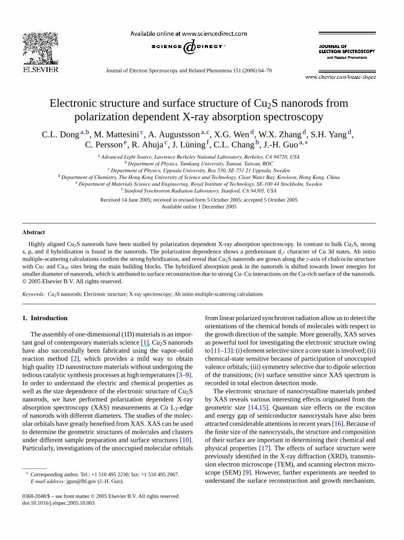
The polarization dependence in the X-ray absorption of thenanorods is also confirmed in our calculations (Fig. 3). The 24different Cu sites are not aligned with a specific orientationd ll theo ant.F tosF ssT ndly,wii gles( im-i t areb ction( s as -mas
a ands con-tt dow.P ardi amed , peakA iza-t er,a ofh ri hich
ld
-
n.d
n
a,-
irection, and the spectrum is therefore an average of arientations of Cu atoms. Two limiting situations are relevirstly, we consider the Cu1 site where the Cu ion is bondedulfur atoms in the plane perpendicular toz-axis[30], as shown inig. 3. In this case, the calculated intensity of peakA1 increaseignificantly with the increased incident angles (seeFig. 3a).his is opposite to the experimental observations. Secohen considering the Cu2S fragment (Cu7 and Cu10) located
n a plane nearly parallel to thez-axis, as shown inFig. 3, thentensity of peakA1 decreases with increased incident anFig. 3b and c). Thus, the XAS spectra of nanorods can be mcked by including only Cu sites in chalcocite structure thaonded to S atoms in planes parallel to the growth direFig. 3d). Hence, the resulting L3-edge can be interpreted aum of atoms having both Cu7 and Cu10 atomic-type arrangeents. This effect clearly indicates that Cu2S nanorods growlong thez-axis of the chalcocite structure with Cu7 and Cu10ites as the main building blocks.
PeakA1 is originated by the unoccupied d states, whileA2ndA3 arise from transitions to empty bands with mixed dcharacters. Their intensity is determined by the different
ribution of the dipole matrix elements (l → l − 1 andl → l + 1)hat weight the partial DOS along the calculated energy winarticularly, the p→ s contribution increases by going upw
n energy, while the p→ d component decreases along the sirection. Because of the isotropic character of the s states2 slightly varies with respect to the variation of the polar
ion vector, while peakA3 remains nearly unchanged. Howevsmall polarization dependence ofA3 indicates some degreeybridization with the in-plane p states. PeakA3 does not appea
n the calculation due to the strict dipole selection rule, w
C.L. Dong et al. / Journal of Electron Spectroscopy and Related Phenomena 151 (2006) 64–70 67
Fig. 3. Calculated polarization dependence of Cu L3-edge X-ray absorption spectra. A sphere of radius 2.5A centered at the absorbing atom was considered for eachCu site (CuS3 fragment) where the sulfur atoms are in a plane perpendicular (Cu7 and Cu10) to or parallel (Cu1) to the [2 0 4] crystal plane.
neglects the p→ p transitions. On the contrary, the experimentalXAS spectra present a weak signal (peakA3) at 938.5 eV thatindicates a mixing between Cu 3d, 4s and Cu 4p.
The large intensity weight on peaksA2 and A3 in theXAS spectra indicates that nanorods have strong hybridizationbetween s, p and d states. This hybridization is very differentfrom bulk Cu2S that has strong Cu-d valence-band character witha little mixing to S-p, which yields a weak Cu–S bond. Therefore,size variations of the Cu2S nanorods can easily change its elec-tronic structure near the band edges. We expect that strong sizedependence of hybridization can be found also in Cu2(Se,Te)binaries as well as in Cu(Al,Ga,In)(S,Se,Te)2 ternaries, whichare important materials in photovoltaic applications, but not inthe II–VI analogue Zn(S,Se,Te) nanostructures which shouldhave much deeper cation-d states and stronger bonds.
The calculated partial density-of-states (DOS) of Cu and S areshown inFig. 4for different cluster sizes of Cu2S. In the first caseone regards the Cu7 atom centered into a relative large atomiccluster with 87 or 36 atoms to mimic the electronic properties ofa bulk-like structure. At the other extreme we have consideredthe Cu7 atom as coordinated by three sulfurs or with additionalfive nearby copper atoms to simulate ions sitting on a nanorods’
surface. Such small CuS3 system was therefore employed inorder to account for the change in the s, p, d hybridization whenthe structure varies from a bulk- to a surface-like system.
The use of several atomic clusters is to reproduce the differents–p–d hybridization in the valence bands (i.e. to monitor thestrength of the Cu–S bond). The results support the observationof the experimental XAS. In the contest of the VB DOS we usedthe 87-atom cluster as representative for the bulk phase. It shouldbe noted here that we were only interested in a qualitative changeof position and shape of Cu-d and S-p states when moving froma “surface-like” to a “bulk-like” system. However, to be moreprecise no significant changes were found in the Cu L3-edge(i.e. unoccupied states) when increasing the cluster size abovethe number of 87 atoms.
As shown inFig. 4, the DOS of bulk Cu2S is mainly con-stituted by S-p and S-d states located at the top of the valenceband and by the Cu-d states positioned at lower energies (seeFig. 4b). As expected, only small hybridization is establishedbetween Cu-d and the S-p states. However, when looking at thesurface-like DOS (Fig. 4a) a clear sharpening of the Cu-d andS-p states is found together with very similar energy positionsand bandwidths. This match of positions and bandwidths indi-

68 C.L. Dong et al. / Journal of Electron Spectroscopy and Related Phenomena 151 (2006) 64–70
Fig. 4. The partial density of states of Cu and S are calculated for different cluster sizes to simulate both surface-like and bulk-like structure in nanorods. The atomicarrangement around the Cu7 site is shown: (a) CuS3 fragment with five neighboring Cu atoms, (b) bulk-like structure with 87 atoms. In small clusters (four and nineatoms) the S-p states hybridizes largely with Cu-s and d states, but in larger systems (36 and 87 atoms) the S-p states move to lower energies resulting in a lesshybridization with the Cu-s and d states.
cates an enhanced degree of hybridization between Cu-d andS-p states and therefore also a strengthening of the Cu–S bond.Moreover, it is interesting to observe that in the smaller clustersystem the valence band maximum presents a larger Cu-s statescontribution, indicating that both s and d states move toward anatomic-like configuration (Cu 3d104s1).
The absorption peaksA1 andA2 of nano #1 shift to higher,respectively, lower energies with respect to nano #2 (Fig. 5a).
This is in accordance with the calculated absorption spectrum(Fig. 5b) after having introduced the contribution of the secondcoordination shell. In this case the centered Cu is coordinatedwith three sulfur and five copper neighboring atoms. The dif-ference between calculation and experiment at the area around932.5 eV is ascribed to the approximations used in the calcu-lation scheme, i.e. muffin-tin potential, exchange functional,cluster size, etc. Thus, the discrepancy at about 932.5 eV does

C.L. Dong et al. / Journal of Electron Spectroscopy and Related Phenomena 151 (2006) 64–70 69
Fig. 5. (a) Experimental X-ray absorption spectra of Cu2S nanorods at incidentangle of 90◦; (b) calculated X-ray absorption for Cu7 site using onlythe firstcoordination shell and bothfirst andsecond coordination shells.
not influence the main conclusions. Therefore, in a qualitativeway, these shifts can be attributed to surface effects caused bthe large number of Cu atoms on the surface and a higher suface pressure in nano #1. This follows from the Cu-rich growthconditions. A large energy shift is observed for peakA′
2 in nano#1 at incident angle 15◦ (see inFig. 2). This significant changecan probably be attributed to the formation of some small clus-ters at the top of the Cu2S nanorods[31]. At incidence of 15◦,there is a dominant contribution from the top of the nanorodswhere some small nanoclusters remain, created at the beginninof the nucleation process. The lack of energy shift for peakA2in nano #2 suggests that the nanoclusters may aggregate to forlarger size of particles after a longer period of growth. Further-more, the shift ofA2 from different diameter of nanorods showsthe same trend predicted by theory, although the shift in spectrum recorded at 15◦ seems to agree better with the calculationof nine-atom cluster. These experimental findings support thegrowth model that the growth reaction takes place on the topof nanorods[9], and that the Cu-rich surface forms a base forthe fluid transport layer that sustains the growth of the Cu2Snanorods.
5. Conclusions
From our X-ray absorption measurements and multiple-scattering calculations, we find that the highly aligned nanorods
show very strong hybridization between s, p, and d states. Thisoriginates from the relatively weak Cu-d–S-p bond that allowschanges in the electronic character with reducing nanorodsdiameter. The polarization dependence of the absorption spec-tra reveals that the Cu 3d states have predominant dz2 character.This is a consequence of a nanorods growth along the chal-cocite z-axis, with Cu7 and Cu10 atomic sites being the mainbuilding blocks. The nanorods have relatively small crystal-fieldsplitting. The shift of the hybridizedA2 peak is attributed to aCu-rich surface with strong Cu–Cu interaction resulted from adiameter-reduced nanorods.
Acknowledgements
The work at ALS and SSRL is funded by the U.S. Departmentof Energy (ALS under Contract No. DE-AC02-05CH11231).The work is also supported by the Swedish Research Council,and by an RGC grant administered by the UGC of Hong Kong.We thank J. Stohr for making his end-station available for themeasurements.
References
[1] C. Joachim, S. Roth, Atomic and Molecular Wires, Kluwer AcademicPublishers, London, 1997.
[2] S.H. Wang, S.H. Yang, Adv. Mater. Opt. Electron. 10 (2000) 39;
95)
ou,
[ Nord-
[[ 1994)
[ nom.
[ osi,
[ 87
[
[
[ atos,
[ 233
[ hys.
[[
[
yr-
g
m
-
S.H. Wang, S.H. Yang, Chem. Phys. Lett. 322 (2000) 567.[3] S. Iijima, Nature 354 (1991) 56.[4] C.R. Martin, Science 266 (1994) 1961.[5] H.J. Dai, E.W. Wong, Y.Z. Lu, S.S. Fan, C.M. Lieber, Nature 375 (19
769.[6] W. Han, S. Fan, Q. Li, Y. Hu, Science 277 (1997) 1287.[7] Z.W. Pan, S.S. Xie, B.H. Chang, C.Y. Wang, L. Lu, W. Liu, W.Y. Zh
W.Z. Li, Nature 394 (1998) 631.[8] A.M. Morale, C.M. Lieber, Science 279 (1998) 208.[9] S.H. Wang, S.H. Yang, Chem. Mater. 13 (2001) 4794.10] J.-H. Guo, L. Vayssieres, C. Persson, R. Ahuja, B. Johansson, J.
gren, J. Phys.: Condens. Matter 14 (2002) 6969.11] J. Stohr, NEXAFS Spectroscopy, Springer, Berlin, 1992.12] F.M.F. de Groot, J. Electron. Spectrosc. Relat. Phenom. 67 (
529–622.13] F.M.F. de Groot, M.F. de Groot, J. Electron. Spectrosc. Relat. Phe
62 (1993) 111.14] M.G. Mason, S.-T. Lee, G. Apai, R.F. Davis, D.A. Shirley, A. Franci
J.H. Weaver, Phys. Rev. Lett. 47 (1981) 730.15] C.L. Chang, C.L. Dong, C.L. Huang, Y.Y. Chen, J. Appl. Phys.
(2000) 3349.16] Y.K. Chang, et al., Phys. Rev. Lett. 82 (1999) 5377;
T. Van Buuren, et al., Phys. Rev. Lett. 80 (1998) 3803.17] J.M. McHale, et al., Science 277 (1997) 788;
S.H. Tolbert, A.P. Alivisatos, J. Chem. Phys. 102 (1995) 4642.18] K.S. Hamad, R. Roth, J. Rockenberger, T. van Buuren, P. Alivis
Phys. Rev. Lett. 83 (1999) 3474.19] N. Wang, K.K. Fung, S.H. Wang, S.H. Yang, J. Cryst. Growth
(2001) 226.20] S.H. Wang, S.H. Yang, Z.R. Dai, Z.L. Wang, Phys. Chem. Chem. P
3 (2001) 3750.21] S.H. Wang, S.H. Yang, Mater. Sci. Eng. C16 (2001) 37.22] A.L. Ankudinov, et al., Phys. Rev. B 58 (1998) 7565;
A.L. Ankudinov, et al., Phys. Rev. B 65 (2002) 104107;J.J. Rehr, R.C. Albers, Rev. Mod. Phys. 72 (2000) 621;S.I. Zabinsky, et al., Phys. Rev. B 52 (1995) 2995.
23] H.T. Evans Jr., Nature 232 (1971) 69;H.T. Evans Jr., Z. Kristallogr. 150 (1979) 299.

70 C.L. Dong et al. / Journal of Electron Spectroscopy and Related Phenomena 151 (2006) 64–70
[24] L. Hedin, B.I. Lundqvist, J. Phys. C 4 (1971) 2064.[25] S. Carniato, Y. Luo, H.Agren, Phys. Rev. B 63 (2001) 085105–085115.[26] M. Grioni, J.B. Goedkoop, R. Schoorl, F.M.F. de Groot, J.C. Fuggle, F.
Schafers, E.E. Koch, G. Rossi, J.-M. Esteva, R.C. Karnatak, Phys. Rev.B. 39 (1989) 1541.
[27] C.F.J. Flipse, G. van der Laan, A.L. Johnson, K. Kadowaki, Phys. Rev.B 42 (1990) 1997.
[28] G. van der Laan, R.A.D. Pattrick, C.M.B. Henderson, D.J. Vaughan, J.Phys. Chem. Solids 53 (1992) 1185.
[29] A.N. Platonov, Nature of the Colors of Minerals, Naukova Dumka, Kiev,1976.
[30] Atomic positions in chalcocite structure: Cu1 (0.8645, 0.2496, 0.2927),Cu7 (0.9345, 0.1233, 0.9923), and Cu10 (0.4429, 0.1477, 0.9348); theCu1 site represents the case where all the three Cu–S bonds are in aplane perpendicular toz-axis (growth direction), whereas the Cu7 andCu10 have Cu–S bonds in a plane parallel toz-axis.
[31] Y. Volokitin, J. Sinzig, L.J. de Jongh, G. Schmid, M.N. Vargaftik, I.I.Mosseev, Nature 384 (1996) 621.
Related Documents