Japanese Technology Evaluation Center JTEC JTEC Panel Report on Electronic Manufacturing and Packaging in Japan Michael J. Kelly, Chair William R. Boulton John A. Kukowski Eugene S. Meieran Michael Pecht John W. Peeples Rao R. Tummala February 1995 International Technology Research Institute R.D. Shelton, Director Geoffrey M. Holdridge, WTEC Director Loyola College in Maryland 4501 North Charles Street Baltimore, Maryland 21210-2699

Welcome message from author
This document is posted to help you gain knowledge. Please leave a comment to let me know what you think about it! Share it to your friends and learn new things together.
Transcript
Japanese Technology Evaluation Center
JTEC
JTEC Panel Report on
Electronic Manufacturing and Packagingin Japan
Michael J. Kelly, ChairWilliam R. BoultonJohn A. KukowskiEugene S. MeieranMichael PechtJohn W. PeeplesRao R. Tummala
February 1995
International Technology Research InstituteR.D. Shelton, Director
Geoffrey M. Holdridge, WTEC Director
Loyola College in Maryland4501 North Charles Street
Baltimore, Maryland 21210-2699

JTEC PANEL ON ELECTRONIC MANUFACTURING AND PACKAGING IN JAPAN
Sponsored by the National Science Foundation, the Advanced Research Projects Agency, the National Aeronautics and SpaceAdministration, and the Department of Commerce of the United States Government
Dr. Michael J. Kelly (Chair)Georgia Institute of TechnologyManufacturing Research Center813 Ferst DriveAtlanta, GA 30332-0560
Dr. William R. BoultonCenter for International CommerceAuburn UniversitySuite 109 Business Building415 West Magnolia Ave.Auburn, AL 36849
Mr. John KukowskiRochester Institute of TechnologyManufacturing Engineering TechnologyJames E. Gleason Building - #978 Lom Memorial DriveRochester, NY 14623-5604
Dr. Gene MeieranIntel Corporation500 W. Chandler BoulevardMS - CH 2-23Chandler, AZ 85226
Dr. Michael PechtCALCE - EPRCUniversity of MarylandCollege Park, MD 20742
Dr. John PeeplesAT&TGlobal Information SolutionsWest Columbia, SC
Dr. Rao TummalaGeorgia Institute of TechnologyManufacturing Research Center813 Ferst DriveAtlanta, GA 30332-0560
INTERNATIONAL TECHNOLOGY RESEARCH INSTITUTEJTEC/WTEC PROGRAM
The Japanese Technology Evaluation Center (JTEC) and its companion World Technology Evaluation Center (WTEC) atLoyola College provide assessments of foreign research and development in selected technologies under a cooperativeagreement with the National Science Foundation (NSF). Loyola's International Technology Research Institute (ITRI), R.D.Shelton, Director, is the umbrella organization for JTEC and WTEC. Paul Herer, Senior Advisor for Planning andTechnology Evaluation at NSF's Engineering Directorate, is NSF Program Director for JTEC and WTEC. Other U.S.government agencies that provide support for the program include the National Aeronautics and Space Administration, theDepartment of Energy, the Department of Commerce, and the Department of Defense.
JTEC/WTEC's mission is to inform U.S. policy makers, strategic planners, and managers about the state of selectedtechnologies in foreign countries in comparison to the United States. JTEC/WTEC assessments cover basic research,advanced development, and applications/commercialization. Small panels of about six technical experts conductJTEC/WTEC assessments. Panelists are leading authorities in their field, technically active, and knowledgeable about U.S.and foreign research programs. As part of the assessment process, panels visit and carry out extensive discussions withforeign scientists and engineers in universities and in industry/government labs.
The ITRI staff at Loyola College help select topics, recruit expert panelists, arrange study visits to foreign laboratories,organize workshop presentations, and finally, edit and disseminate the final reports.
Dr. Michael J. DeHaemer Mr. Geoff Holdridge Dr. George GamotaPrincipal Investigator JTEC/WTEC Staff Director Senior Advisor to JTEC/WTECLoyola College Loyola College Mitre CorporationBaltimore, MD 21210 Baltimore, MD 21210 Bedford, MA 01730
JTEC Panel on
Electronic Manufacturing and Packaging in Japan
FINAL REPORT
February 1995
Michael J. Kelly, ChairWilliam R. BoultonJohn A. KukowskiEugene S. MeieranMichael PechtJohn W. PeeplesRao R. Tummala
William R. Boulton, Editor
ISBN 1-883712-37-8This document was sponsored by the National Science Foundation (NSF), the Advanced ResearchProjects Agency, the National Aeronautics and Space Administration, and the Department ofCommerce of the United States Government under NSF Cooperative Agreement ENG-9217849,awarded to the International Technology Research Institute at Loyola College in Maryland. Anyopinions, findings, and conclusions or recommendations expressed in this material are solely those ofthe authors and do not necessarily reflect the views of the United States Government, the authors'parent institutions, or Loyola College.

ABSTRACT
This report summarizes the status of electronic manufacturing and packaging technology inJapan in comparison to that in the United States, and its impact on competition in electronicmanufacturing in general. In addition to electronic manufacturing technologies, the reportcovers technology and manufacturing infrastructure, electronics manufacturing and assembly,quality assurance and reliability in the Japanese electronics industry, and successful productrealization strategies. The panel found that Japan leads the United States in almost everyelectronics packaging technology. Japan clearly has achieved a strategic advantage inelectronics production and process technologies. Panel members believe that Japanesecompetitors could be leading U.S. firms by as much as a decade in some electronics processtechnologies. Japan has established this marked competitive advantage in electronics as aconsequence of developing low-cost, high-volume consumer products. Japan’s infrastructure,and the remarkable cohesiveness of vision and purpose in government and industry, are keyfactors in the success of Japan’s electronics industry. Although Japan will continue todominate consumer electronics in the foreseeable future, opportunities exist for the UnitedStates and other industrial countries to capture an increasingly large part of the market. TheJTEC panel has identified no insurmountable barriers that would prevent the United Statesfrom regaining a significant share of the consumer electronics market; in fact, there isample evidence that the United States needs to aggressively pursue high-volume, low-costelectronic assembly, because it is a critical path leading to high-performance electronicsystems.
JTEC/WTEC
Michael J. DeHaemer, Principal Investigator, DirectorGeoffrey M. Holdridge, Staff Director and JTEC/WTEC Series Editor
Bobby A. Williams, Assistant DirectorCatrina M. Foley, Secretary
Aminah Batta, Editorial AssistantPatricia M.H. Johnson, Editor
Advance Work performed by M. Gene Lim of SEAM International
International Technology Research Institute at Loyola College
R. D. Shelton, Director
Copyright 1995 by Loyola College in Maryland except as otherwise noted. The U.S. Government retains anonexclusive and nontransferable license to exercise all exclusive rights provided by copyright. The ISBNnumber for this report is 1-883712-37-8. This report is distributed by the National Technical InformationService (NTIS) of the U.S. Department of Commerce as NTIS Report # PB95-188116. Information on orderingfrom NTIS and a list of JTEC/WTEC reports available from NTIS are included on the inside back cover of thisreport.

i
FOREWORD
The National Science Foundation (NSF) has been involved in funding technologyassessments comparing the United States and foreign countries since 1983. A sizableproportion of this activity has been in the Japanese Technology Evaluation Center (JTEC)and World Technology Evaluation Center (WTEC) programs. NSF has supported more thanthirty JTEC and WTEC studies over a wide range of technical topics.
As U.S. technological leadership is challenged in areas of previous dominance such asaeronautics, space, and nuclear power, many governmental and private organizations seek toset policies that will help maintain U.S. strengths. To do this effectively requires anunderstanding of the relative position of the United States and its competitors. The purposeof the JTEC/WTEC program is to assess research and development efforts in other countriesin specific areas of technology, to compare these efforts and their results to U.S. research inthe same areas, and to identify opportunities for international collaboration in precompetitiveresearch.
Many U.S. organizations support substantial data gathering and analysis efforts directed atnations such as Japan. But often the results of these studies are not widely available. At thesame time, government and privately sponsored studies that are in the public domain tend tobe "input" studies; that is, they provide enumeration of inputs to the research anddevelopment process, such as monetary expenditures, personnel data, and facilities, but donot provide an assessment of the quality or quantity of the outputs obtained.
Studies of the outputs of the research and development process are more difficult to performbecause they require a subjective analysis performed by individuals who are experts in therelevant technical fields. The NSF staff includes professionals with expertise in a wide rangeof disciplines. These individuals provide the technical expertise needed to assemble panelsof experts that can perform competent, unbiased, technical reviews of research anddevelopment activities.
Specific technologies, such as telecommunications, biotechnology, microelectromechanicalsystems, and nuclear power, are selected for study by government agencies that have aninterest in obtaining the results of an assessment and are able to contribute to its funding. Atypical assessment is sponsored by two to four agencies. In the first few years of the program,most of the studies focused on Japan, reflecting concern over Japan's growing economicprowess. Studies were largely defined by a few federal mission agencies that contributedmost of the funding, such as the Department of Commerce, the Department of Defense, andthe Department of Energy.
The early JTEC methodology involved assembling a team of U.S. experts (usually six peoplefrom universities, industry, and government), reviewing the extant literature, and writing a

ii
final report. Within a few years, the program began to evolve. First we added site visits.Panels traveled to Japan for a week and visited twenty to thirty industrial and research sites.Then, as interest in Japan increased, a larger number of agencies became involved ascosponsors of studies. Over the ten-year history of the program, fifteen separate branches insix agencies of the federal government (including NSF) have supported JTEC and WTECstudies.
Beginning in 1990, we began to broaden the geographic focus of the studies. As interest inthe European Community (now the European Union) grew, we added Europe as area ofstudy. With the breakup of the former Soviet Union, we began organizing visits to previouslyrestricted research sites opening up there. These most recent WTEC studies have focused onidentifying opportunities for cooperation with researchers and institutes in Russia, theUkraine, and Belarus, rather than on assessing them from a competitive viewpoint.
In the past four years, we also have begun to substantially expand our efforts to disseminateinformation. Attendance at JTEC/WTEC workshops (in which panels present preliminaryfindings) has increased, especially industry participation. Representatives of U.S. industrynow routinely number 50 percent or more of the total attendance, with a broad cross sectionof government and academic representatives making up the remainder. JTEC and WTECstudies have also started to generate increased interest beyond the science and technologycommunity, with more workshop participation by policymakers and better exposure in thegeneral press (e.g., Wall Street Journal, New York Times). Publications by JTEC and WTECpanel members based on our studies have increased, as have the number of presentations bypanelists at professional society meetings.
The JTEC/WTEC program will continue to evolve in response to changing conditions in theyears to come. NSF is now considering new initiatives aimed at the following objectives:
• Expanding opportunities for the larger science and technology community to help defineand organize studies.
• Increasing industry sponsorship of JTEC and WTEC studies. For example, NSF recentlyfunded a team organized by the Polymer Science and Engineering Department at theUniversity of Massachusetts (Amherst) for a two-week visit to Japan to studybiodegradable plastics and polymers R&D. Twelve industrial firms provided over half ofthe funds.
• Providing a broader policy and economic context to JTEC/WTEC studies. This isdirected at the need to answer the question, "So what?" that is often raised in connectionwith the purely technical conclusions of many JTEC and WTEC panels. What are theimplications of the technical results for U.S. industry and the economy in general? Aneconomist has joined the current JTEC study on optoelectronics in Japan as part of a neweffort to address these broader questions.

iii
In the end, all government-funded programs must answer the question, How has the programbenefited the nation? A few of the benefits of the JTEC/WTEC program follow:
• JTEC studies have contributed significantly to U.S. benchmarking of the growingprowess of Japan's technological enterprise. Some have estimated that JTEC has beenresponsible for over half of the major Japanese technology benchmarking studiesconducted in the United States in the past decade. JTEC reports have also been widelycited in various competitiveness studies.
• These studies have provided important input to policymakers in federal mission agencies.JTEC and WTEC panel chairs have given special briefings to senior officials of theDepartment of Energy, to the National Aeronautics and Space Administration (NASA)Administrator, and even to the President's Science Advisor.
• Studies have been of keen interest to U.S. industry, providing managers with a sense ofthe competitive environment internationally. Members of the recently completed studyon satellite communications have been involved in preliminary discussions concerningthe establishment of two separate industry/university consortia aimed at correcting thetechnological imbalances identified by the panel in its report.
• Information from JTEC and WTEC studies also has been valuable to both U.S. andforeign researchers, suggesting a potential for new research topics and approaches, aswell as opportunities for international cooperation. One JTEC panelist was recently toldby his Japanese hosts that, as a result of his observations and suggestions, they haverecently made significant new advances in their research.
• Not the least important is the educational benefit of the studies. Since 1983 over 200scientists and engineers from all walks of life have participated as panelists in the studies.As a result of their experiences, many have changed their viewpoints on the significanceand originality of foreign research. Some have also developed lasting relationships andongoing exchanges of information with their foreign hosts as a result of their participationin these studies.
As we seek to refine the JTEC/WTEC program in the coming years, improving themethodology and enhancing the impact, program organizers and participants will continue tooperate from the same basic premise that has been behind the program from its inception: theUnited States can benefit from a better understanding of cutting-edge research that is beingconducted outside its borders. Improved awareness of international developments cansignificantly enhance the scope and effectiveness of international collaboration and thusbenefit all of the United States' international partners in collaborative research anddevelopment efforts.
Paul J. HererNational Science FoundationArlington, VA

iv
v
TABLE OF CONTENTS
Foreword .............................................................................................................................. iContents .............................................................................................................................. vList of Figures .................................................................................................................. viiiList of Tables....................................................................................................................... xPreface................................................................................................................................ xi
Executive Summary........................................................................................................ xv
1. Microelectronics in JapanWilliam R. Boulton
Introduction............................................................................................................. 1The U.S. Electronics Industry ................................................................................. 3Japan's Electronics Industry .................................................................................... 5The Microelectronics Industry Structure............................................................... 16References............................................................................................................. 20
2. Building the Electronic Industry’s RoadmapsWilliam R. Boulton
Dimensions of Product Development in Japan..................................................... 21Conclusions........................................................................................................... 34References............................................................................................................. 34
3. Japan's Technology and Manufacturing InfrastructureWilliam R. BoultonEugene S. MeieranRao R. Tummala
Overview of Japan's Technology Infrastructure.................................................... 35Japan’s Technology Development Strategy .......................................................... 37Japan’s Product Development Strategy................................................................. 42Industrial Computerization ................................................................................... 48Electronics Research Activities............................................................................. 49Hitachi’s R&D Structure....................................................................................... 52Conclusion ............................................................................................................ 58References............................................................................................................. 58

Contentsvi
4. Japan's Electronic Packaging TechnologiesRao R. TummalaMichael Pecht
Introduction............................................................................................................59Japan's Electronic Packaging Strategies ................................................................60Plastic Packaging Technologies.............................................................................63Ceramic Packaging Technologies..........................................................................72Passive Component Technologies .........................................................................78Advanced Multichip Packaging Developments.....................................................79Printed Wiring Board Technologies ......................................................................83Chip Assembly Technologies ................................................................................86Package Assembly Technologies...........................................................................90Future Package Decisions ......................................................................................92Summary Of Japanese Packaging Trends..............................................................95Conclusion .............................................................................................................95References..............................................................................................................95
5. Electronics Manufacturing and Assembly in JapanJohn A. KukowskiWilliam R. Boulton
Japan's Distinctive Competence In Manufacturing................................................97Enabling Technologies.........................................................................................106Factory Automation (FA).....................................................................................107Japan’s Automated Electronics Assembly Demonstrated ...................................111Summary..............................................................................................................114References............................................................................................................114
6. Quality Assurance and Reliability in the Japanese Electronics IndustryMichael PechtWilliam R. Boulton
History of Japan's Quality Movement..................................................................115Quality and Reliability Requirements..................................................................118Summary..............................................................................................................125References............................................................................................................125
7. Successful Product Realization StrategiesJohn PeeplesWilliam R. Boulton
Requirements Definition......................................................................................127Design for Excellence..........................................................................................129Japanese Technology Commercialization Efforts................................................136Summary..............................................................................................................146References............................................................................................................146

Contents vii
APPENDICES
A. Professional Experience of Panel Members.................................................... 147
B. Professional Experience of Other Team Members........................................ 152
C. Site Reports
Fujitsu.................................................................................................................. 155Hitachi PERL, HIMEL........................................................................................ 160Ibiden................................................................................................................... 165Matsushita Electric.............................................................................................. 170Matsushita-Kotobuki Electronics........................................................................ 174Meisei University ................................................................................................ 178Murata ................................................................................................................. 186Nippondenso ....................................................................................................... 190Nitto Denko......................................................................................................... 195Oki....................................................................................................................... 200Sony..................................................................................................................... 208TDK .................................................................................................................... 217
D. Sponsors of the JTEC Study on Electronic Packaging in Japan.................. 222
E. Attendees of the Industrial Representatives Meeting on April 19, 1993...... 223
F. Glossary.............................................................................................................. 224

viii
LIST OF FIGURES
E.1 Mass production strategy for low-cost electronic products .................................... xxii
1.1 1991 global electronics production; the four largest electronics regions.................61.2 Japan’s trading relationships in 1993.......................................................................91.3 The movement of Japanese production facilities offshore ....................................101.4 Japanese forecast of audiovisual production in 1995 and 2000.............................141.5 Number of computer-related systems worldwide ..................................................151.6 Microelectronics world market structure 1990 ......................................................17
2.1 Strategic objectives for product development........................................................222.2 First-to-market advantages.....................................................................................242.3 Financial advantages for product leadership..........................................................242.4 Next-generation product roadmaps........................................................................272.5 Market-driven demands for electronic packaging..................................................28
3.1 Japan’s successful production development strategy.............................................383.2 Parallel product development strategies in Japan ..................................................403.3 TDK’s product development strategy ....................................................................413.4 Japanese passive component strategy ....................................................................413.5 Japan’s product development strategy ...................................................................423.6 Moore’s Law of Active Element Density ..............................................................443.7 PC board component density .................................................................................453.8 Hitachi’s distribution of R&D funds .....................................................................533.9 Hitachi's Strategic Business Projects system .........................................................57
4.1 Japan’s technological and market leadership.........................................................604.2 Japanese competitive advantage from breadth of technology................................614.3 Mass production strategy for low-cost electronic products ...................................614.4 Electronic packaging trends...................................................................................624.5 Single chip packaging costs ...................................................................................644.6 Current development trends of epoxy molded compounds ...................................664.7 Ceramic packaging trends......................................................................................734.8 Consumer ceramic substrate ..................................................................................744.9 Low-cost ceramic co-firing process with copper ...................................................744.10 Consumer ceramic substrate with Cu ....................................................................754.11 Multilayer ceramic (MLC) and printed wiring board (PWB) compared ...............754.12 Hollow structure in ceramic for improved dielectric constant...............................764.13 Propagation delay versus dielectric constant .........................................................764.14 Package design improvement ................................................................................774.15 Ceracom substrate with low TCE and low dielectric constant ..............................774.16 Components trend in camcorders...........................................................................78

Figures ix
4.17 Overall Japanese packaging strategy..................................................................... 804.18 Flip chip processing conductive adhesive............................................................. 804.19 QFP-MCM in ceramic .......................................................................................... 814.20 Wiring density comparison between PWB/ceramic.............................................. 824.21 Low-cost fine line thin film process...................................................................... 844.22 Shape and accuracy of conductor pattern by additive process .............................. 854.23 Additive process enhancement.............................................................................. 854.24 Anisotropic conductive conductor system ............................................................ 864.25 Nitto process for TAB........................................................................................... 884.26 Nitto bump making process .................................................................................. 884.27 Microprocessor carrier (BGA) for LSI.................................................................. 894.28 Bump fabrication process...................................................................................... 894.29 Effects of encapsulation on strain in solder .......................................................... 904.30 Effects of encapsulation and solder composition on strain in solder .................... 904.31 Japanese consumer product component density trend .......................................... 904.32 Soldering defect improvement achieved at Oki .................................................... 914.33 Soldering technology trend in Japan ..................................................................... 924.34 Package weight versus pin count .......................................................................... 934.35 Lead pitch and mounting height............................................................................ 934.36 High pin count packages ....................................................................................... 934.37 Relative package areas: BGA versus QFP ............................................................ 934.38 Japanese high pin count strategy........................................................................... 944.39 Japanese packaging assembly strategy.................................................................. 94
5.1 Japan’s development of computer-integrated manufacturing ............................. 1005.2 Japan’s surface mount devices............................................................................ 1035.3 Japan’s SM applications of major components................................................... 1045.4 Major companies comprising Japan’s surface mount infrastructure................... 1055.5 Japan’s surface mount developments.................................................................. 1055.6 Next-generation surface mount technology ........................................................ 1065.7 Predominant pitch capability for low-cost electronic packaging ........................ 109
6.1 Cause-and-effect diagram ................................................................................... 117
7.1 Japan’s product development activities .............................................................. 1307.2 Concurrent development requirements ............................................................... 1317.3 Functional integration required for technological innovations ........................... 1327.4 Concurrent engineering for product innovation.................................................. 1337.5 Murata’s integrated technology strategy ............................................................. 1377.6 Sony’s concurrent development model ............................................................... 1387.7 Sharp’s expanding LCD applications.................................................................. 1417.8 NEC’s technology planning process ................................................................... 1447.9 NEC’s contract and budget process .................................................................... 145
x
LIST OF TABLES
E.1 Packaging Technology Leadership (U.S. Compared to Japan)............................ xvi
1.1 Japan's Electronics Industry Production 1992-3, Forecast for 1994........................71.2 Japan’s Consumer Electronics Production 1992-3, Forecast for 1994 ....................71.3 Export Ratios of Major Export Items ......................................................................91.4 The Number of Offshore Japanese Production Bases in 1992...............................111.5 Japan’s Electronics Imports in 1992, by Region ...................................................121.6 Japanese R&D Expenditures .................................................................................131.7 Electronic Devices and Parts Output .....................................................................16
2.1 1993 First-Half Performance of Japanese Electronics Companies........................252.2 Packaging Technology for the 21st Century ..........................................................292.3 Logic LSI Package Roadmap.................................................................................312.4 Matsushita Video Camera Board Designs .............................................................32
3.1 Japanese Major Electronics Firms' Capital & R&D Investments ..........................503.2 Hitachi Limited's Corporate Research Laboratories ..............................................543.3 Hitachi Corporate Research Funding.....................................................................55
4.1 Molding Compound Development in Japan ..........................................................654.4 Future Plastic PGA Technology................................................................................ 684.2 Development Roadmap of Semiconductor Encapsulating Material ......................694.3 Development Roadmap of Semiconductor Encapsulating Material (Part 2).........704.5 Memory Package (TSOP) Technology Roadmap..................................................714.6 Logic LSI Package Roadmap.................................................................................724.7 Japanese Ceramic Substrate Materials...................................................................734.8 NEC’s Ceramic Roadmap......................................................................................764.9 Component Miniaturization...................................................................................784.10 Nitto Denko's Blend Polymer Dielectric................................................................824.11 Characteristics Of Additive-Plated PWB...............................................................854.12 Japanese Chip Assembly Plan (Oki)......................................................................874.13 Japanese TAB Package (TCP) Characteristics (Oki).............................................884.14 Advantages of the Nitto Process ............................................................................884.15 Japanese Packaging Technology Trends................................................................95

xi
PREFACE
This report of the Japanese Technology Evaluation Center (JTEC) began in late 1992 whenfour agencies of the United States Government contacted JTEC to request a study ofhigh-volume, low-cost electronic packaging in Japan. The four agencies that contractedthis study were the Department of Commerce (DOC), the National Science Foundation(NSF), the National Aeronautics and Space Administration (NASA), and the AdvancedResearch Projects Agency (ARPA) of the Department of Defense (DOD). During ameeting held in Washington, DC, on January 8, 1993, representatives from the sponsoringagencies (listed in Appendix D) met with JTEC staff to identify their respective interests inthe study. DOC through its charter to assess and report on Japanese technology, and NSFas the lead agency for JTEC, both were primarily interested in the technologies ofelectronics packaging in Japan; NASA was primarily interested in the reliability ofelectronics components for spacecraft; and ARPA was primarily interested in assessing therelative strengths of commercial industrial electronics products in the United States andJapan, because of DOD’s commitment to increase procurements of affordable componentsin the commercial marketplace. The representatives from the four sponsoring agenciesagreed that the basic goal for the study should be identification of the factors that havemade Japan so successful in the field of high-volume electronics.
On request from the sponsors JTEC sought industrial input on the value of such a study toU.S. industry. Dr. Michael J. Kelly, Director of the Manufacturing Research Center atGeorgia Tech, agreed to chair the JTEC Electronics Packaging Panel and to organize themeeting to solicit recommendations from the industrial sector. The meeting was held inWashington, D.C., on April 19, 1993. Attendees (listed in Appendix E) generally agreedthat Japanese competitive advantages in electronics are based on more than technology.They argued for a study that also investigated the impact of infrastructure, management,investment, and government policies on Japan's dominance in the electronic marketplace.In response to these recommendations, JTEC selected a panel of experts with diversebackgrounds that would enable them to address multiple facets of electronicsmanufacturing and packaging in Japan. Following is a brief biography of each of the panelmembers. More detailed biographies of the panelists and of other participants in theJapanese site visits are included in this volume as Appendices A and B, respectively.
Dr. Michael Kelly, the panel chair, is Director of the Manufacturing Research Center atGeorgia Tech. Prior to his present position he was Director of the Defense ManufacturingOffice at the Advanced Research Projects Agency at the Department of Defense. Heworked for IBM between 1969 and 1987.
Dr. William Boulton is a professor of strategic management and Director of the Center forInternational Commerce at Auburn University. Dr. Boulton has spent seven years inmanagerial and academic positions in Japan, including Visiting Scholar at Japan’s Ministry

Prefacexii
of Finance’s Institute for Fiscal and Financial Policy, and Visiting Professor at KeioUniversity’s Graduate School of Business Administration.
Mr. John Kukowski is a corporate fellow at Universal Instruments Corporation, where healso held the position of Vice President of Advanced Technology. Mr. Kukowski ispresently on sabbatical at Rochester Institute of Technology, where he is assisting in thedevelopment of an interdisciplinary electronics design and manufacturing program.
Dr. Gene Meieran is an Intel Fellow whose knowledge of the electronic “food chain,”beginning with materials, has established him as a leader in the electronics industry. Inaddition to his Intel responsibilities, Dr. Meieran is also Director of Research for the MITLeaders for Manufacturing program.
Dr. Michael Pecht is a professor at the University of Maryland where he is also founderand director of the Computer Aided Life Cycle Engineering (CALCE) ElectronicPackaging Research Center. Dr. Pecht is chief editor of IEEE’s Transactions onReliability.
Dr. John Peeples is an Assistant Vice President of Manufacturing for AT&T GlobalInformation Solutions (formerly NCR) and Director of the Manufacturing TechnologyResearch Center. Dr. Peeples is also the leader of the Director of Engineering Peer Teamfor the General Purpose Product Group.
Dr. Rao Tummala is a recognized expert in high-performance electronic packaging who, asan IBM Fellow, was responsible for IBM's advanced electronic packaging program.Dr. Tummala is now a chaired professor in the Electrical Engineering Department atGeorgia Tech.
On May 4, 1993, the JTEC electronics packaging (EP) panel met with its sponsors andJTEC staff in Washington, D.C., to clarify the objectives of the electronics packagingstudy. The attendees identified four primary areas for assessment:
1. Japanese technology priorities and roadmaps
2. Japanese product realization processes, with specific attention to notebooks, personaldigital assistants, camcorders, and cellular telephones
3. Japan’s competitive advantages related to manufacturing and production technology
4. Japan’s competitive advantages related to infrastructure and management supportsystems
Dr. Gene Lim of SEAM International worked closely with the panel to arrange meetingswith appropriate companies in Japan between October 1-9, 1993. The panel members werejoined in Japan by Dr. Nick Naclerio of ARPA; Mr. Phil Barela of NASA; Mr. GeorgeHarman of DOC; Dr. Linton Salmon of NSF; Dr. Duane Shelton of JTEC; and Dr. Lim.
Preface xiii
Subsequent to the site visits, panelists and other team members generated a report on eachsite. These site reports are included in this report as Appendix C. JTEC held an openmeeting in Washington, D.C., on January 12, 1994, during which the JTEC ElectronicPackaging Panel reported its preliminary findings.
Following the workshop, the panel members prepared the first draft of the written reportthat is published in this volume. Both the site reports and the draft chapters were subjectedto an extensive review process. During the course of this review, extensive new andupdated information was added by both Japanese hosts and panel members. Duringproofing of the report prior to publication, more new information derived from recentpublications was added. The end result that follows is the JTEC panel’s final evaluation.
The content of the analytical chapters of this report, Electronic Manufacturing andPackaging in Japan, was contributed by the panel members. Michael Kelly prepared theExecutive Summary; William Boulton edited the chapters in draft. The authors of the bodyof the report are as follows: William Boulton describes the importance of the electronicsindustry to global competition in Chapter 1, High-Volume Low-Cost Electronic Packaging.Dr. Boulton also provides a conceptual understanding of the product developmentproblems for electronics as described in Chapter 2, Building the Electronic Industry'sRoadmaps. Gene Meieran, William Boulton, and Rao Tummala developed Chapter 3,Japan's Technology and Manufacturing Infrastructure, to describe some of the underlyingstrengths of Japan’s electronic industry. Rao Tummala and Michael Pecht provide thetechnological descriptions in Chapter 4, Japan’s Electronic Packaging Technologies. JohnKukowski and William Boulton offer a description of Japan’s electronic manufacturingcapabilities in Chapter 5, Electronic Manufacturing and Assembling in Japan. MichaelPecht and William Boulton are the authors of Chapter 6, Quality Assurance and Reliabilityin the Electronic Industry. John Peeples and William Boulton contributed the material forChapter 7, Successful Product Realization Strategies.
The authors of this report are deeply indebted to the large number of people whocontributed to its preparation. We extend our sincere thanks to our Japanese hosts who sograciously gave of their time in sharing information about their respective companies. Wealso appreciate the cooperation of the sponsoring agencies and the contributions of theirrepresentatives who accompanied the JTEC panel; these were major factors in thesuccessful development of the report. We are greatly indebted to Dr. Gene Lim who madethe excellent trip preparations to Japan and accompanied us during our visits to theJapanese companies. Finally, the panel members wish to express our appreciation to all themembers of the JTEC staff, especially Geoff Holdridge, for their cheerfully given supportin preparing for the study, executing it, and publishing the results.

Prefacexiv

xv
EXECUTIVE SUMMARY
This study of electronic manufacturing and packaging in Japan grew out of a widespreadinterest on the part of U.S. government and industry leaders to understand the strengths ofJapan’s electronics industry as a step towards improving the vitality of the U.S. electronicsindustry. The Japanese Technology Evaluation Center (JTEC) assembled the electronicpackaging and manufacturing panel in 1993 at the request of four U.S. Government agencies:the Advanced Research Projects Agency of the Department of Defense, the Department ofCommerce, the National Aeronautics and Space Administration, and the National ScienceFoundation. The purpose of the study was defined in consultation with industry advisors: toevaluate the technologies, processes, priorities, and supporting infrastructures that haveallowed Japan to achieve dominance of the global electronics marketplace. The JTECelectronics packaging and manufacturing panel visited Japan from October 1-9, 1993, thenreported its findings at an open meeting in Washington, D.C., on January 12, 1994. Thiswritten report is based on the panel’s observations during site visits; on dialogues withcolleagues in Japanese companies, universities, and professional associations; and onliterature published subsequent to the panel’s site visits.
PRINCIPAL CONCLUSIONS
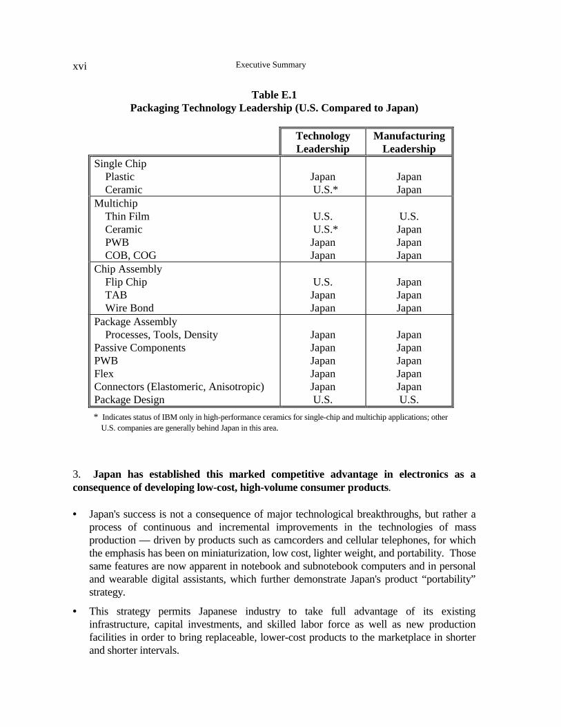
The JTEC panel on electronic manufacturing and packaging confirmed its expectations:Japan has the most advanced electronic assembly manufacturing processes in the world. TheUnited States must learn the lessons of Japan and become a world-class manufacturer.
1. Japan leads the United States in almost every electronics packaging technology.Comparisons of electronic packaging technologies in Japan and the United States (as in TableE.1) reveal that, while some U.S. companies lead in specific ceramic technologies and in thetechnologies of thin film multichip modules (MCMs), flip chip assembly, and packagedesign, Japanese firms are the leaders in all other packaging categories.
2. Japan clearly has achieved a strategic advantage in electronics production andprocess technologies. Panel members believe that Japanese competitors could beleading U.S. firms by as much as a decade in some electronic process technologies.
• Because process technology improvements allow for quality improvements and costreductions in end products, Japan’s continuous perfection of its electronics manufacturingsystems has enabled it to take market leadership away from technology innovators in theUnited States.
• Furthermore, it is apparent that due to its successes in process improvement, Japan will bea primary world supplier not only of electronics products and components, but also ofelectronics manufacturing equipment.
Executive Summaryxvi
Table E.1Packaging Technology Leadership (U.S. Compared to Japan)
TechnologyLeadership
ManufacturingLeadership
Single Chip Plastic Ceramic
Japan U.S.*
JapanJapan
Multichip Thin Film Ceramic PWB COB, COG
U.S. U.S.*JapanJapan
U.S.JapanJapanJapan
Chip Assembly Flip Chip TAB Wire Bond
U.S.JapanJapan
JapanJapanJapan
Package Assembly Processes, Tools, DensityPassive ComponentsPWBFlexConnectors (Elastomeric, Anisotropic)Package Design
JapanJapanJapanJapanJapanU.S.
JapanJapanJapanJapanJapanU.S.
* Indicates status of IBM only in high-performance ceramics for single-chip and multichip applications; other U.S. companies are generally behind Japan in this area.
3. Japan has established this marked competitive advantage in electronics as aconsequence of developing low-cost, high-volume consumer products.
• Japan's success is not a consequence of major technological breakthroughs, but rather aprocess of continuous and incremental improvements in the technologies of massproduction — driven by products such as camcorders and cellular telephones, for whichthe emphasis has been on miniaturization, low cost, lighter weight, and portability. Thosesame features are now apparent in notebook and subnotebook computers and in personaland wearable digital assistants, which further demonstrate Japan's product “portability”strategy.
• This strategy permits Japanese industry to take full advantage of its existinginfrastructure, capital investments, and skilled labor force as well as new productionfacilities in order to bring replaceable, lower-cost products to the marketplace in shorterand shorter intervals.
JTEC Panel on Electronic Manufacturing and Packaging in Japan xvii
4. Japan’s infrastructure, and the remarkable cohesiveness of vision and purpose ingovernment and industry, are key factors in the success of Japan’s electronics industry.
• Long-term product development roadmaps provide the technology pull required tostimulate supplier investments in critical technologies and equipment essential for timelyintroduction of next-generation consumer electronic products.
• Overall industry structure and supporting institutions promote continuous, long-termtechnical and process improvements that sustain Japan’s competitive position in low-costconsumer electronics and ensure the quality and reliability of products.
• Product development involves the highest levels of management to ensure that resourcesare available for concurrent engineering of new products.
• Weaknesses in these areas are major contributors to U.S. industry being unable to fullyexploit technological innovations derived from extensive R&D investments, as occurredwith integrated circuits and flat panel displays.
5. Although Japan will continue to dominate consumer electronics in the foreseeablefuture, opportunities exist for the United States and other industrial countries tocapture an increasingly large share of the market.
• The United States in particular controls much of the technology that will drive futureconsumer electronics: telecommunications, computers, microprocessors, and software.
• The challenge for the United States is to exploit its technological advantages bybecoming the low-cost producer of high-volume electronic products. Recentstreamlining and restructuring of U.S. industry, combined with increased capitalinvestments, have paid big dividends. The U.S. worker is now the most productive inthe world. These developments provide the United States with major competitiveadvantages.
6. The JTEC panel identified no insurmountable barriers that would prevent theUnited States from regaining a significant share of the consumer electronics market;in fact, there was ample evidence that the United States needs to aggressively pursuehigh-volume, low-cost electronic assembly, because it is a critical path leading to high-performance electronic systems.
• The United States has the technological edge, as was demonstrated recently by itsadvances in high definition television. Japan has the edge in production technology, andit is expected to continue to be the world leader in high-precision electronic assembly.The country that excels in both new technology and production technology will lead theworld in consumer electronics.
• Advanced technology continues to be the heritage of the United States; if a similar focuscan be placed on production technology, the United States can capture a dominant shareof the consumer market. Continuous corporate reengineering, an emphasis on concurrent
Executive Summaryxviii
development, partnering between suppliers and customers, and further commitment toenhancing the skills of the workforce are critical success factors that must be addressed.In the words of Robert Hayes (1981, 66), “We must compete with the Japanese as they dowith us: by always putting our best resources and talent to work doing the basic things alittle better, every day, over a long period of time. It is that simple — and that difficult.”
The Japanese can do it; Americans can do it. The issue that separates the United States fromJapan in high-volume, low-cost electronic assembly is neither technology nor manufacturing;it is primarily the will to take the measures necessary to compete and succeed.
BACKGROUND
The electronics industry is a vital part of the U.S. economy. It is "the largest manufacturingemployer in the United States…[accounting] for nearly 11% of the U.S. gross domesticproduct. It is expected to grow at a rate of 4% per year throughout the remainder of the1990s" (MCC 1992). The United States has developed or is developing many of the state-of-the-art technologies on which the world electronics trade depends; also, the U.S. electronicsindustry has invested more money in R&D than have its foreign competitors. Despite thesestrengths, U.S. electronics manufacturers have steadily lost market share to foreign-owned orforeign-based manufacturers in practically every electronics sector. According to Ross(1992), “the U.S. electronics industry has been losing about 3% of world market share peryear since the mid-1980s, a market that today is about three-quarters of a trillion dollars andis expected to be $2 trillion by the beginning of the next century."
While the United States has lost ground in the world electronics marketplace, Japan hassteadily improved its competitive position; it is now the recognized world leader in theproduction of consumer electronics products. U.S. firms have abandoned the markets formany consumer electronics products, and so there has been little incentive to keep up withJapanese firms in improving low-cost, high-volume electronic packaging and assemblyequipment technologies. Without the incentives and profits of staying competitive in theconsumer marketplace, however, there is much evidence that the U.S. electronics industry haslost its ability to efficiently produce top-notch, reasonably priced electronics components forthe industrial and military — as well as the consumer — sectors. Furthermore, electronicsproducts have come to represent a significant portion of the U.S.-Japan trade imbalance. In1992 Japan's electronic exports to the United States were valued at $30.4 billion, 32% of itstotal exports to the United States; in that year the United States had a negative trade balancewith Japan of $7.3 billion in consumer electronics and $7.8 billion in computers andperipheral equipment (ITTRI 1994). These trends give U.S. policymakers and electronicsmanufacturers ample cause for concern.
The term “electronic packaging” today means the production and assembly of a great manytypes of increasingly tiny and complex electronic circuitry components and boards central tothe design and low-cost assembly of electronic products. Japan’s manufacture of products
JTEC Panel on Electronic Manufacturing and Packaging in Japan xix
like camcorders, palmcorders, handycams, VCRs, and cellular phones has simultaneouslydriven the miniaturization of electronic packaging and a corresponding advancement ofassembly technologies. These popular consumer electronic products utilize a relatively largeamount of analog circuitry, which has pushed the Japanese to develop cost-effectiveprocesses for assembling high-density miniaturized passive components. The use of “1005”packages (100 mm x 50 mm) and smaller formats requires both leading-edge surface mountprocess capabilities and ultrasmall component developments. That is, Japan’s successesderive not only from production of advanced devices but also from development of newequipment and procedures to manufacture and emplace those devices. This studyinvestigates both electronic packaging technologies per se and also related manufacturingtechnologies. In response to the widespread notion that the United States needs to betterunderstand “the realities of Japanese industry,” this study also investigates goal-setting andinfrastructure in the electronics industry of Japan.
CREATING A VISION OF THE FUTURE
Chapter 2 provides a model of Japan’s vision of future product development activities. Theintroduction of next-generation components and equipment corresponds to the introduction ofnext-generation products. At Sony, next-generation products are defined as half the size andhalf the weight at the same cost. Roadmaps signal industry suppliers about future customerrequirements. The panel found that in Japan
• Long-term product planning accompanies a product-pull investment strategy. TheJapanese will continue to make major R&D investments that are product driven.
• The guiding principle for management is product planning, which leads to efficientinvestments in technology and production; the best technology is the most affordabletechnology.
• The focus on cost, size, and weight reduction drives the miniaturization process;however, there may be a limit to ultrasmall assembling.
The changes taking place in consumer electronics have significant implications for the future.Companies in the high-volume electronics business are on a steep learning curve that isproviding continuous opportunities to fuse technologies to meet product objectives. This ismost evident in the flat panel display technology that is merging traditional electronics withdisplays.
It appears that component vendors are moving toward supplying functional modules, andsystem integrators are becoming increasingly aware of the benefits of also manufacturingcomponents. Sony, for example, now manufactures about 65% of the key components of thecompact disc player. There is evidence that companies like Murata and Nippondenso areseeking increased independence through technology and component self-sufficiency. Asvendors provide more of the subsystem integration and component costs increasingly dictate

Executive Summaryxx
profits, the relationships between suppliers and end-product producers may change. At thetime of the JTEC team’s visit, however, there was no indication of any lessening of thetraditional supplier-customer interdependencies. Subcontractors contribute to new productdevelopment, and technical information is widely shared among vendors and end-productintegrators. This organizational structure lends itself to effective concurrent development,shorter development cycle times, and lower life-cycle costs.
As the fusion of technologies increases and semiconductors, electronic packages, displays,and peripheral devices become increasingly integrated, the electronics industry may undergomajor restructuring; it is not evident who will have the major advantage. It is clear thatadvanced technology and flexible manufacturing will not, by themselves, provide theadvantage; nor will excellence in design. Organizations capable of quickly responding tochange, led by visionary and capable management, will hold the essential competitiveadvantage. The lesson from Japan is that teaming is a primary success factor.
SUPPORTING INFRASTRUCTURES
Chapter 3 provides an overview of the infrastructure that supports Japan’s leadership inconsumer electronics. The panel found that
• Japanese firms appoint a greater number of technically trained managers to head theircompanies than do U.S. firms.
• Corporate enterprises are structured and managed to operate effectively in the globalmarketplace.
• Firms have separated research on production technologies from other research anddevelopment activities.
• Enterprises invest heavily in the development of production automation technology.
• Japan’s patent system functions to facilitate industry-wide transfer of technology ratherthan to protect intellectual property rights.
• Industrial research is given additional support through local municipal industrial researchinstitutes (MIRIs).
• Japanese firms are constantly in pursuit of new technical knowledge and effective transferof technology from global sources.
• Recent recessionary pressures are temporary and may actually strengthen the industry.
• People are the primary sustainable competitive advantage. Information technology can beemployed to support continuous learning; it is not, however, a substitute for the kind oftraining and personal communication evidenced in Japan.
• The borderless manufacturing world is a continuing reality that justifies furtherinvestments in transportable manufacturing-enabling technologies.
JTEC Panel on Electronic Manufacturing and Packaging in Japan xxi
The existing infrastructure supports movement into advanced technologies and products. Thisis particularly evident in the electronics industries. Separation of production developmentfocuses attention and resources on manufacturing advancements that ensure the rapidintroduction of new, high-quality products at low costs. Without advanced equipmentcapabilities, it would take much longer for new component technologies to become part ofnext-generation product designs. The strategic importance of manufacturing is emphasized inthe education of the workforce and in the priority that management gives to continuouslyimproving the process in order to more rapidly and efficiently manufacture complex products.
The United States has lost the infrastructure necessary to be globally competitive in theproduction of high-volume, low-cost electronic products, despite the fact that U.S. industrymay dominate certain sectors such as microprocessors. While the United States continues toinvest heavily in R&D, Asia is making major investments in manufacturing infrastructure.U.S. investments in R&D are now being exploited offshore, with associated negative effectson jobs, the balance of trade, and the general economic health of the country. Domesticsuppliers have been abandoned in favor of low-cost offshore producers that frequently receivethe latest technologies from their customers.
PACKAGING TECHNOLOGIES
Chapter 4 explores Japan's technology packaging strategy. It is important to understand notonly what technology Japan is developing, but also how firms pursue their objectives. TheJTEC panel's findings in this regard indicate that Japanese companies
• Seek to identify customer needs as the basis for developing next-generation products thatestablish the roadmaps for technological development.
• Make long-term commitments to component and equipment development that supportfuture product innovations.
• Effectively utilize existing investments in the established supplier base and existingtechnological infrastructure; investments in new technologies are introduced only whencompetitive challenges require them.
Miniaturization is expected to continue to place pressure on packaging technologies and theirassembly. In both the United States and Japan, the rate of silicon scale integration willcontinue to improve semiconductor cost and performance through the 1990s assemiconductor suppliers develop systems on a chip. At the next level in the “food chain,” thefocus in the 1990s will be on high-density electronic assembly technologies. Many of thegains in the 1990s will be attained through continuous improvements in Japan’s existingsurface mount packaging and assembly technologies, leading to devices with improvedfunctionality, input/outputs in excess of 1,000, lead pitches below 0.2 mm, low-cost MCMs,
and improvements in equipment technology to meet the requirements shown in Figure E.1.Specifics of the Japanese roadmaps for achieving these goals are provided in the report.

Executive Summaryxxii
Figure E.1. Mass production strategy for low-cost electronic products.
The drive toward smaller, thinner, and lighter high-pin-count packages is expected to besatisfied initially through the employment of thin quad flat pack, tape automated bonding, andpin grid array. The ball grid array will be available for applications exceeding 600 pins. Flipchip technology is being extensively pursued by most Japanese companies. Of particularinterest is direct bonding of a bumped chip to a printed wiring board (PWB) using a low-temperature solder that is hot injection deposited onto the PWB through a mask. While thereare continuing technical problems that need to be solved, such as the development of athermally compatible encapsulant, success will permit Japanese investments in PWB to beincrementally improved over the next decade to meet consumer product requirements. Thereis evidence of merging technologies to meet new high-volume product demand: MCMs areappearing in both supercomputers and camcorders, and electronic drivers are fusing with flatpanel displays.
PRODUCTION TECHNOLOGIES
Chapter 5 discusses production capabilities in electronic packaging. It was evident to theJTEC panel that Japanese manufacturing excellence is a consequence of the tight coupling offunctions within each company and with respective suppliers. Major collaboration amongindustrial partners and between government and industry, as conclusively demonstrated inJapan, is required to sustain a competitive posture in the high-volume, low-cost electronicsbusiness.
Critical Technologies: Electronic Packaging Advances
Objective: Low Cost Products
Strategy: Develop Volume Markets & Mass Production Technologies
QFP 1.0 x 0.5 mm size 100 µm lines 0.4 mm pitch 250 µm vias
6 - 8 layers
TQFP 0.8 x 0.4 mm 50 µm lines 0.15 mm TAB built-in 50 µm vias pitch capacitors, 100 µm pitch resistors, inductors 8 layers
Plastic Discrete PWB SMTPackages ComponentsTechnology
Today
Tomorrow(Year 2000)

JTEC Panel on Electronic Manufacturing and Packaging in Japan xxiii
Japanese industry as a whole has focused a massive amount of resources on the design anddevelopment of complex automated equipment, and the range of equipment developmentexpertise within individual companies is tremendous. That expertise covers all thetechnological areas required to be self-sufficient and dominant in this field. The consensus inJapan is that equipment provides a major competitive advantage and that equipmentdevelopment technology is mandatory in order to lead in the introduction of new products.The panel also found that • Equipment is the key to advanced manufacturing; it must be an integral part of
technology development.
• Investments required for automation to achieve precision assembly, manpower reduction,and agility must be balanced against requirements based on modular product design andmodular assembly.
• Continuous improvements in existing processes avoid capital investments, retraining, andrisks associated with the introduction of new technology.
Component miniaturization, cost reduction, reduced development cycle times, andimprovements in reliability and quality require continued advancement in production andprocess technologies. Production requirements will include more affordable andenvironmentally safe materials; flexible and automated equipment linked to affordablemanufacturing processes; cost-effective and accurate testing; effective partnering withsuppliers and enterprise teaming; continuous process improvements; and innovative, user-friendly designs. Increased demands for chip attach technologies will supplement currentsurface mount technology. Differences between technological alternatives will fade astechnologies converge and hybrid electronic assemblies become commonplace in integratedsystems.
The principal technologies that have provided competitive advantages include surface mounttechnology and flexible assembly technologies capable of responding to high-volumeproduction with multiple product variations. While Japanese companies continue to do R&Din advanced process technology, it appears evident that surface mount technologies willcontinue to dominate consumer products into the next century. Mounting methods willbecome more sophisticated and include greater levels of chips and direct bonding of bumpedchips. Mounting densities will increase to 50 components per square centimeter. Passivecomponents are expected to reach their size limitation at 0.8 mm x 0.4 mm before they areintegrated into modules. Pin pitches will be as low as 0.15 mm. Low-cost resin boardtechnologies will reach 50 micron lines and 50 micron vias with eight layers.
In the consumer electronics of the future, it will be increasingly difficult to separate integratedcircuits, electronic packages, and flat panel displays. While continuous improvements can beexpected in materials, equipment, and design tools, it will be the flexible, automated,adaptive manufacturing processes that will provide the primary competitive advantage. It isproduction technology that is making Japan the leader in high-volume, low-cost electronics,and it appears evident that this same strength will continue into the future.
Executive Summaryxxiv
QUALITY AND RELIABILITY
Chapter 6 describes Japan’s approach to quality and reliability. Japanese firms appear to seekout the root causes of quality and reliability problems. This has led Japanese producers tofocus on continuous improvements in materials, equipment, and processes. Quality isconsidered the cost of entry; low product cost is considered the requirement for success.
Suppliers that are able to provide the required quality components at the appropriate time andcost will be the future market winners. To assure product quality, every Japanese supplierhas had to resolve materials, equipment, and processes problems. Component suppliers oftendesign future manufacturing processes in order to be “first to market” with new components.Next-generation production systems are developed for next-generation products. In order tofully exploit capital investments and to minimize variability and product defects in themanufacturing process, these new systems are only reluctantly changed once installed.
PRODUCT REALIZATION
Chapter 7 summarizes many of the comprehensive activities that make up Japanese firms’strategy of product development. The panel reached several conclusions about productrealization in Japan:
• Product realization encompasses concurrent development, teaming, a supportiveinfrastructure, and a strategy of continuous improvement.
• Short development cycles, low cost, high volume, and innovative designs are responses tomajor customer requirements and competitive pressures.
• Major organizational commitments are being made and resources obligated to developnext-generation components and products.
• Continuous improvement of existing technology, in contrast to frequent introduction ofnew technology, appears to be a winning strategy. Anticipating technologicaldiscontinuities and planning for change are the main challenges for management.
Japan is investing to sustain its advantage through continuing to develop new materials,packaging, designs, equipment, and improvements to production processes. It was obviousthat many companies had built competitive advantages by developing next-generationcomponents, like charge-coupled devices for video cameras and liquid crystal displays forportable TVs and notebook computers. These components have given Sony a 75% marketshare in 8 mm video cameras and Sharp a major share in calculators and portable digitalassistants. Today companies are seeking to use these component advantages to introduceinnovative products like Sharp’s new ViewCam. Cost pressures will accelerate globalmanufacturing partnerships, but Japan will continue to control many of the enablingproduction and component technologies used in next-generation packages.

JTEC Panel on Electronic Manufacturing and Packaging in Japan xxv
Once they have developed a market, Japanese firms have maintained market leadershipthrough continuous improvement of existing products. Concurrent engineering allows forshort product development cycles, as short as six months for Sony’s Walkman products.Plans for next-generation products are managed by senior executives who have access toneeded resources to push for rapid technological development. This next-generation product-pull scenario is linked to a long-term product strategy for which the primary focus isaffordability.
An industrial country cannot survive on technology alone. Unlike Japan, the United Stateshas not fully understood that technology must be exploited through the manufacture ofproducts in sufficient volume to generate the data — as well as profits — that are the basis ofcontinuous improvement. Without the data generated by high-volume production, there arefundamental limits to improving manufacturing processes. The sought-after six-sigmaprocess is directly dependent on the generation of significant data to evaluate a fullproduction process.
The driver for electronics technologies has shifted from semiconductors to electronicassemblies, which are giving rise to new families of products that rival the integration of thecamera and recorder. The telecomputer is the next high-volume consumer product. Theword is a compound descriptive that links television and computer, telecommunications andcomputer, telephone and computer. Next will be the electromobile, with transportationincreasingly dominated by the introduction of more and more electronics. There are thosewho are already referring to cars of the future as "chips on wheels." With more than fiftyelectric motors in some cars, the term "motor vehicle" is taking on a whole new meaning.
CONCLUSIONS
The JTEC study on electronic manufacturing and packaging in Japan, as described in thisreport, makes it very clear that Japan dominates electronic production technology. The reportfurther demonstrates that Japan’s success can be directly linked to a product-pull strategy thathas the effect of exploiting new technology quickly. While Japan continues to invest inresearch and development of new technology, the dominant influence is in the process ofcontinuous improvement of existing technologies to meet the cost, size, weight, and powerrequirements of the consumer market including portable electronic products. The strategy ofcontinuous improvement is also considered the key to satisfying cycle-time reductionrequirements.
When describing future consumer electronics there is a major focus on the multimedia unitsthat will be found in seamless networks where data, voice, and graphical information aretransmitted almost instantaneously. The cost of electronics is expected to continuedecreasing at its present rate until, as Edward McCracken, CEO of Silicon Graphics,suggests, “We must make available $150 to $300 systems providing realtime audio and videoprocessing” (1994, 3). In the area of multimedia and networking technology, the United
Executive Summaryxxvi
States continues to be in a very strong position; however, Japan and other Asian countriestotally dominate consumer electronics. The JTEC panel is in full agreement that the UnitedStates must regain a prominent position in high-volume, low-cost electronics, and must do soquickly. As Peter Drucker has said, “A degenerative disease will not be cured byprocrastination. It requires decisive action” (1994, 95). The decisive action is thecommitment to exercise control over the enabling technologies which, when integrated, willproduce the electronic systems that will be found at the nodes of the digital highways. It is anuphill struggle, but it is a challenge that must be accepted if the United States is to be globallycompetitive.
The competitors are not just the Japanese. In 1994, Taiwan was providing about 81% of theworld’s merchant motherboards; procurement by Japan of PC products in Taiwan is projectedto reach $1.4 billion in 1996. South Korea is aggressively moving into consumer electronicswith companies like Samsung expected to produce up to 90,000 AMLCD flat panel displayunits per month by the second quarter of 1995. China has become the country of choice forlow-cost manufacturing, and it will continue to work with foreign countries to introduce high-tech production capabilities. Japan is increasingly moving to offshore production in order tomeet cost requirements. Haruo Tsuji, president of Sharp, has pointed out that, “Theproduction cost in Japan has become the highest in the world.” He goes on to say, “Japan isbecoming a supplier of components and production machinery, like robots, to be used byother nations to assemble the final products” (1994, 3-1).
The JTEC panel did not see anything that would prevent U.S. companies from recapturing asignificant share of future consumer products. However, as Drucker notes, “It requiresdecisive action.” Certainly the United States’ strong position in software can be used to itsadvantage, but even in that realm, Americans must be prepared for challenges from countriessuch as India.
Short product development cycles and product life cycles are causing companies likeCompaq to produce more of their components locally because of the need for shorter deliverytimes. For many multinationals, however, “locally” means to “build where you sell.” TheUnited States is still the world’s largest growth market and, therefore, can exploit the timeparameter and build locally for its own market. There is a need, however, to prepare for thefuture when the Asia Pacific region will be the world’s greatest growth market and “buildwhere you sell” takes on new economies of scale.
We can be encouraged by some recent advances in manufacturing which have demonstratedthat some U.S. companies have learned how to become low-cost producers. In somecompanies this has been done by applying their expertise in developing design tools that areeffectively linked to production systems. In other cases the customer requirements are tightlycoupled with production systems permitting product customization and fast turn-around. Thepeople-free automated facilities that have characterized many high-volume production areasare giving way to skill-based, worker-enabling technologies that characterize agile productionsystems.
JTEC Panel on Electronic Manufacturing and Packaging in Japan xxvii
While the JTEC panel is optimistic that the United States is making progress in improving itsmanufacturing capability, there is no doubt that Japan will continue to be the country tobenchmark against. There is one major concern: the winners in the future will be thosecountries whose workforces are effectively educated and trained to meet the challenges of21st century production. In that regard the United States may be seriously at risk. Thesuperior educational systems in some emerging nations, combined with decades of overseasenrollment and foreign students returning from American universities, is encouraging U.S.multinationals to be increasingly dependent on foreign sources for their required talent and isresulting in research and development following manufacturing offshore.
The semiconductor industry roadmap is targeting 0.07 micron geometry capabilities by theyear 2010 (SIA 1994). During that period, electronic packaging will have to adapt toaccommodate the more stringent semiconductor ground rules. The exploitation of thesetechnologies to meet the demands of the consumer marketplace is what will differentiate thewinners from the losers. The United States must regain its preeminence in consumerelectronics to retain its position as a technology leader. As Oscar Wilde once said, “The oneduty we owe to history is to rewrite it.” The United States must rewrite history to regainconsumer electronics, and it must improve its educational system to produce graduates thatmeet future workforce requirements.
In many respects, the JTEC panel conclusions are neither encouraging nor discouraging. Thepanel saw much to be concerned about when comparing Japanese packaging technology andmanufacturing with similar efforts in the United States. It appears, however, that the race intothe future has many competitors at the starting gate. The winners will be those whoeffectively exploit technology and manage global resources to reduce cycle time and meetproduct affordability criteria. The United States must commit to win; coming in second isbeing the first loser.
REFERENCES
Drucker, Peter. 1994. “The Theory of Business.” Harvard Business Review (Sept.-Oct.): 95.
Hayes, Robert H. 1981. “Why Japanese Factories Work.” Harvard Business Review (July-August):57-66.
ITT Research Institute (ITTRI). 1994. Manufacturing Competitiveness Frontiers. Vol. 18, Nos. 1and 2 (January/February): 23.
MCC/Sandia National Laboratory. 1992 (September). "Industrial Competitiveness in the Balance: ANet Technical Assessment of North American vs. Offshore Electronics Packaging Technology"(report).
McCracken, Edward. 1994. Electronic Buyers’ News. (Oct. 24): 3.
Ross, Ian. 1992. Star Ledger, 5.
Semiconductor Industry Association (SIA). 1994. The National Technology Roadmap forSemiconductors. San Jose, CA.
Tsuji, Haruo. 1994. New York Times (Oct. 23): 3-1.

Executive Summaryxxviii

1
CHAPTER 1
MICROELECTRONICS IN JAPAN
William R. Boulton
The purpose of this JTEC study is to evaluate Japan’s electronic manufacturing andpackaging capabilities within the context of global economic competition. To carry outthis study, the JTEC panel evaluated the framework of the Japanese consumer electronicsindustry and various technological and organizational factors that are likely to determinewho will win and lose in the marketplace. This study begins with a brief overview of theelectronics industry, especially as it operates in Japan today. Succeeding chapters examinethe electronics infrastructure in Japan and take an in-depth look at the central issues ofproduct development in order to identify those parameters that will determine futuredirections for electronic packaging technologies.
INTRODUCTION
Our lives are being revolutionized by electronics. The ways we work, communicate, shop,bank, travel, and learn are changing radically. And whereas natural resources, labor, andcapital once determined a nation’s wealth, today technology — in aerospace, computers,telecommunications, and consumer electronics — significantly affects a nation's wealthand security. Communications, computers, and control technologies are merging to createnew multimedia capabilities for use in business, education, and entertainment. Advancedtechnologies like superconductivity promise a whole new range of capabilities in anotherdecade. Miniaturization of existing products will put libraries and supercomputers into ourbriefcases. The range of future opportunities is bounded only by the ability of ourindustries to utilize these new capabilities in developing next-generation products.

1. Microelectronics in Japan2
Production of high-quality, low-cost consumer electronics products is dependent onproficiency in electronic packaging technologies. Continuous improvement of packagingand related technologies has provided the impetus for development of new and improvedconsumer electronic products; likewise, consumer demand for new and improvedelectronic products at reasonable prices has provided the impetus for development ofincreasingly sophisticated electronic packaging. The most explosive improvements in low-cost, high-volume packaging for consumer products have been in Japan, precisely becauseJapan has been relentlessly pursuing the markets for consumer electronics. The UnitedStates is recognized for developing new technologies; Japan is recognized for continuouslyimproving “old” technologies and pushing the technological limits of their applications inorder to keep their costs down. In doing so, Japanese electronics firms have pushedelectronic packaging into a whole new realm.
In the past, the term “electronic packaging” referred to a small number of formats forencasing electronic components, including integrated circuits, so they could readily andreliably be installed in electronic end-products. The principal packaging types werethrough hole, surface mount, tape automated bonding, single-chip, and multichip, and alsopackaging configurations like dual inline packages (DIP), small inline packages (SIP), andquad flat packages (QFP). Generally, the companies that specialized in manufacturingelectronic packages did not participate in integrating them into the final products.
During several of the JTEC panel’s site visits in Japan, it was evident that electronicpackaging suppliers are integrating forward into both functional modules and integratedassemblies. TDK is making complex multichip modules with densities of 33 units percubic centimeter. Murata is using its materials technology competence to develop and sellradio frequency (RF) components. Most suppliers now develop their own equipment andprovide customers with the assembly equipment required to utilize their new components.At the same time, some of the major electronics companies are manufacturing more oftheir own electronic components based on in-house R&D. Sony, for example,manufactures about 65% of the key components for its compact disc player and 45% of thecomponents for its 8 mm camcorder. In-house advances in liquid crystal display (LCD),charge-couple device (CCD), and electronic packaging technologies were all needed torealize these products.
Consumer products that have been pulling the development of technological advances inelectronic packaging include VCRs, cellular telephones, camcorders, personal digitalassistants, and notebook computers. The goals that define the roadmaps for electronicpackaging development for these products are miniaturization, portability, increasedfunctionality, and cost reduction — in order to capture and retain consumer markets. Thesegoals are being achieved through reduction of parts sizes and increased integration oftechnologies and functions. Electronic packaging technologies have seen increased pincounts, reduced pin pitch, and increased functional densities through the application ofsurface mounting techniques. Reduction in sizes of parts includes reductions in battery anddisplay dimensions. For example, the reduction in the overall size of cellular phones from

William R. Boulton 3
500 cc in 1987 to 150 cc in 1991 was due to a variety of reductions in parts sizes thatincluded the following:
• Power amp size was reduced by reducing part sizes and ICs.
• Filter size was reduced by reducing part sizes and using advanced designs.
• Controller size was reduced through development of special ASICs.
• Battery size was reduced after intermittent receiving methods cut power consumption.
• Board size was reduced by using smaller and thinner 0.5 mm pin pitch LSIs and1.0 mm x 0.5 mm passive parts in new circuit design.
Electronic packages now are becoming hybrid assemblies. Displays are being integratedwith electronic drivers, flex cards are being designed for the flexibility to be manipulated tofit into restricted areas, and the form factor of power supplies is being designed to conformto available spaces within products. The rapid integration of functions within electronicproducts is likely to continue: Japanese firms are all working on merging technologies likeintegrated circuits, electronic packaging, and flat panel displays. At some point an“electronic package” will likely consist of all the electronic and electrical components of aproduct, ultrasmall in size and custom-configured for the product.
The technologies covered by the term “electronic packaging” are evolving rapidly. Thisreport examines this process in terms of the goals, infrastructure, specific technologicalachievements, and dynamics of the electronics industry in Japan.
THE U.S. ELECTRONICS INDUSTRY
The United States is losing technological and market leadership in the world as itselectronics companies drop out of consumer product markets. Today's global competitiveenvironment requires that companies be first to introduce attractive products of the highestquality at the lowest price. Although the United States has long been both a technologyinnovator and a market leader, in the last decade it has been losing strength in themarketplace. According to the National Advisory Committee on Semiconductors (1992, 2),
At the beginning of a decade that promises unprecedented growth in global high-technology markets, the U.S. firms competing in these markets are experiencingdisturbing weaknesses. Many high-volume electronics products, from low-costgoods to highly complex merchandise, are already manufactured overseas. Inaddition, concern is growing about the ability of U.S. firms to remain competitivein markets where they traditionally have been strong, such as low-cost segments ofthe computer and office equipment markets. Across the entire world electronicsmarkets, the share produced by U.S.-owned firms has fallen by 14 percentagepoints since 1985. The market share loss translates to more than $100 billion inlost revenues, given the size of the current world electronics markets.
1. Microelectronics in Japan4
U.S. electronics manufacturers have lost market share to foreign-owned or foreign-basedmanufacturers in practically every electronics sector. This occurred while U.S. industry'sR&D investment exceeded that of foreign competitors, and while U.S. Government R&Ddwarfed that of foreign governments. The Commerce Department was concerned thatJapan could surpass the United States in production of electronic goods by 1994 andemphasized that since 1984 (except for software and medical equipment) the United Stateslost market share in 35 of 37 electronics categories. There are many who believe that theproblem is the U.S. R&D structure’s relative inattention to commercial applications, andthat Americans must improve their focus on the basic problems of technology applicationand prototyping of new products. Bert Haskell of Kodak has stated the following:
North America must develop a…low cost, high technology manufacturinginfrastructure. This can only be accomplished through a commitment tomanufacturing consumer products, and in particular consumer electronics. NorthAmerican companies must identify emerging high volume consumer electronicsproducts, and must be determined to participate broadly in the manufacture ofthese systems (MCC/Sandia 1993).
The United States also lags behind Japan in flexible automated manufacturing. Japanoperates over 68% of all installed industrial robots in the world, compared to only 12.5%operated by the United States. Japan also has over 40% of the world's installed flexiblemanufacturing systems. Driven by the shortening of product life cycles and the growingsegmentation of markets, Japanese companies are committed to improving manufacturingsystem flexibility. While this is costly, it has the associated advantages of making possiblerapid response to new product introductions. Continuous improvements in manufacturingas well as component technologies resulted in Sharp successfully introducing three newmodels of its 8 mm ViewCam within one year of introducing the original product. Insophisticated, flexible electronic assembly equipment, Japanese companies are dominant.
Proficiency in manufacturing high-technology consumer products is critical to maintenanceof U.S. prosperity and leadership in a global marketplace; this is in turn dependent onelectronic packaging proficiency. It is therefore likely that electronic packagingcapabilities will play an increasingly important role in the future economic competitivenessof the United States. The MCC/Sandia report on electronic packaging (1993, 3-4)concluded the following:
• North American companies lead the world in several important segments of theIntegrated Circuit [IC] market, but this lead is weakened by an ill-equipped lowcost packaging infrastructure.
• Japanese IC packaging and assembling technology is significantly superior toNorth American capability in terms of miniaturization and cost effectiveness.
• The Japanese are the global leaders in manufacturing cost effective high densityprinted circuit boards [PCBs]. This leadership has resulted from a gradualimprovement in high volume PCB fabrication processes for consumer electronics.
William R. Boulton 5
• Japanese manufacturers' experience in consumer electronics has given them asignificant edge over their global competitors in fabricating and deployingminiaturized connectors and passive chip components.
• Japanese market share in consumer electronics has created the "product pull"required to justify large investments in manufacturing processes.
• While cost effective multichip modules [MCMs] are only beginning to emerge,Japanese manufacturers find themselves with a large share of the critical consumerelectronics applications which will require MCMs. Japanese manufacturers’dominance of consumer video and PC memory card markets gives them a strategicadvantage over North American manufacturers in amortizing the cost of newMCM processes.
• Japanese leadership in flat panel display fabrication is well known. Thepackaging of display modules, however, also provides Japanese manufacturerswith a high volume application with which to distribute the cost of innovativepackaging process developments.
The latest generation of consumer products is being integrated to provide new products forhome and office: camcorders, electronic still cameras, mini-compact disc players, digitalcompact cassettes, hand-held televisions, and computers. Other consumer products includeportable facsimile machines, copiers and printers, electronic data books, laptop computers,optical disk mass storage systems, smart cards, and portable telephones. Such productsgrew from 5% to more than 45% of Japanese electronics production between 1978 and1988, an average growth rate of over 20% per year, as compared to 10% for the electronicsindustry overall (Dataquest 1988, 4-7). Focusing on high-volume consumer electronicsmarkets has been central to Japan's economic strategy. High-volume products have beenestimated to account for at least one-third of global integrated chip consumption. U.S.companies have depended for 40-50% of the value added in their electronic products onforeign competitors, from whom they purchased large numbers of “upstream” electronicpackages and components (IEEE 1989, 7). The majority of these imported products andtechnologies have come from Japan’s electronics industry.
JAPAN'S ELECTRONICS INDUSTRY
Of the $652 billion in global electronics production in 1991, Japan’s productionrepresented about 27%, as shown in Figure 1.1. Japan's electrical and electronics industryas a whole produced $176 billion in goods in 1991, second only to the United States’ $232billion. In consumer electronics, Japan produced ¥4.7 trillion in goods, a 48% share ofworld production, as compared to shares of 12% for the United States, 22% for WesternEurope, and 18% for newly industrialized economies (NIEs). In industrial electronics,Japan produced ¥11.7 trillion in goods, a 22% share of world production, as compared toshares of 38% for the United States, 34% for Western Europe, and only 6% for the NIEs.In electronic components, Japan produced ¥8.8 trillion in goods, a 37% share of worldproduction, compared to shares of 32% for the United States, 18% for Western Europe, and
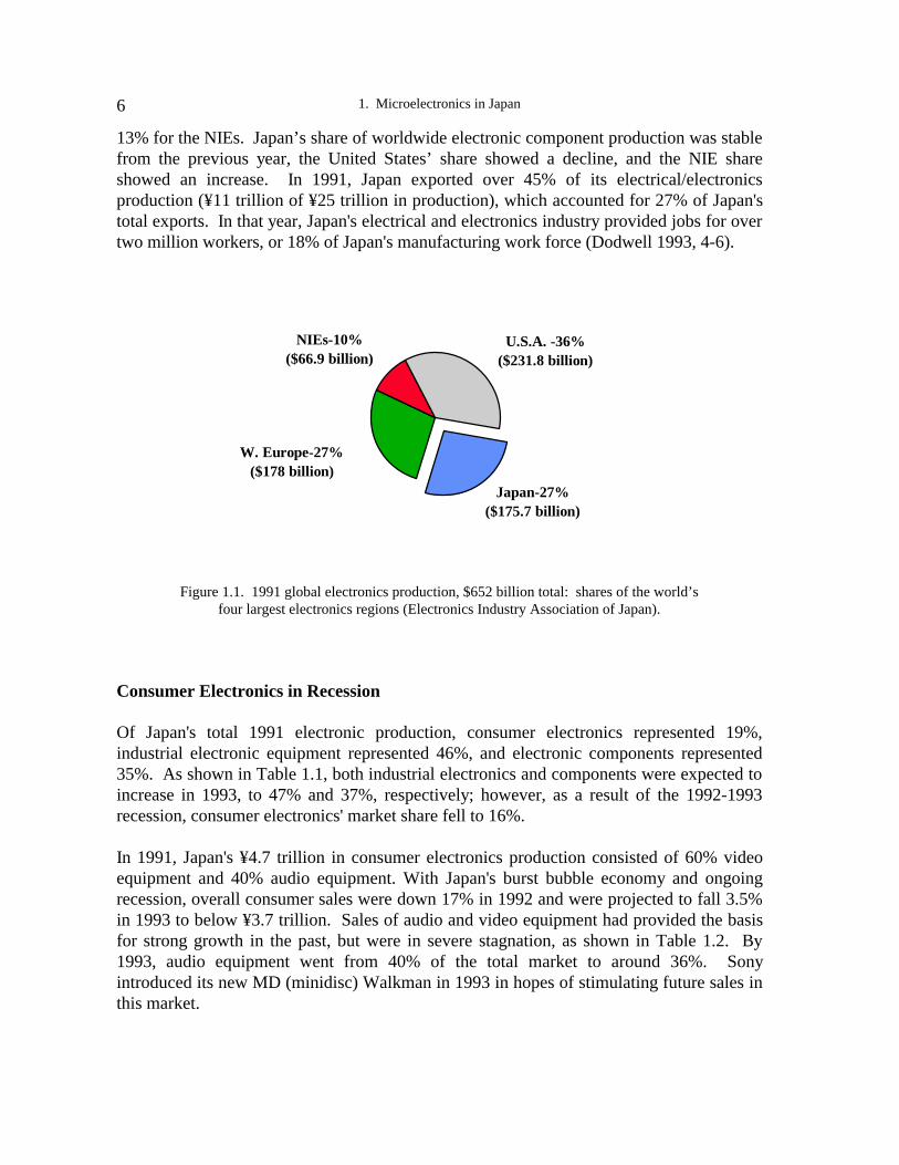
1. Microelectronics in Japan6
13% for the NIEs. Japan’s share of worldwide electronic component production was stablefrom the previous year, the United States’ share showed a decline, and the NIE shareshowed an increase. In 1991, Japan exported over 45% of its electrical/electronicsproduction (¥11 trillion of ¥25 trillion in production), which accounted for 27% of Japan'stotal exports. In that year, Japan's electrical and electronics industry provided jobs for overtwo million workers, or 18% of Japan's manufacturing work force (Dodwell 1993, 4-6).
W. Europe-27%($178 billion)
NIEs-10%($66.9 billion)
U.S.A. -36%($231.8 billion)
Japan-27%($175.7 billion)
Figure 1.1. 1991 global electronics production, $652 billion total: shares of the world’sfour largest electronics regions (Electronics Industry Association of Japan).
Consumer Electronics in Recession
Of Japan's total 1991 electronic production, consumer electronics represented 19%,industrial electronic equipment represented 46%, and electronic components represented35%. As shown in Table 1.1, both industrial electronics and components were expected toincrease in 1993, to 47% and 37%, respectively; however, as a result of the 1992-1993recession, consumer electronics' market share fell to 16%.
In 1991, Japan's ¥4.7 trillion in consumer electronics production consisted of 60% videoequipment and 40% audio equipment. With Japan's burst bubble economy and ongoingrecession, overall consumer sales were down 17% in 1992 and were projected to fall 3.5%in 1993 to below ¥3.7 trillion. Sales of audio and video equipment had provided the basisfor strong growth in the past, but were in severe stagnation, as shown in Table 1.2. By1993, audio equipment went from 40% of the total market to around 36%. Sonyintroduced its new MD (minidisc) Walkman in 1993 in hopes of stimulating future sales inthis market.
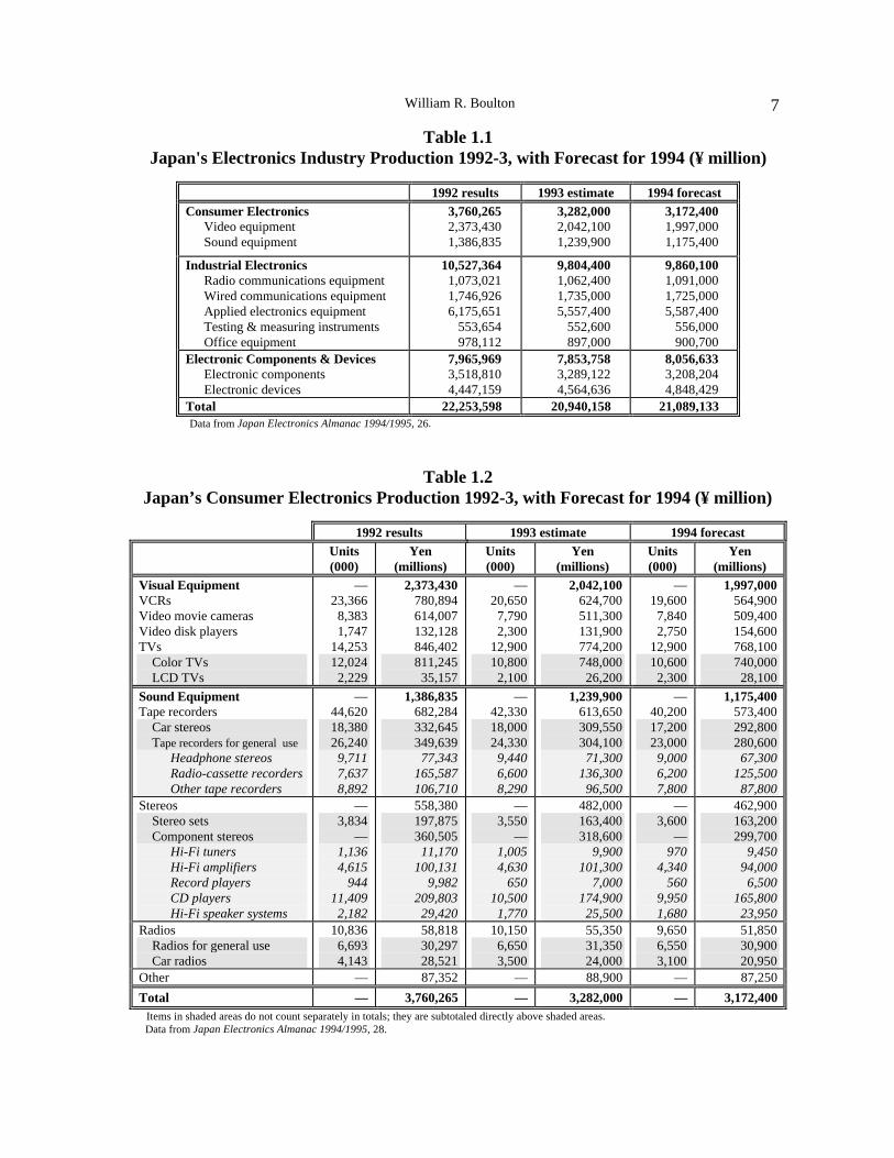
William R. Boulton 7
Table 1.1Japan's Electronics Industry Production 1992-3, with Forecast for 1994 (¥ million)
Data from Japan Electronics Almanac 1994/1995, 26.
Table 1.2Japan’s Consumer Electronics Production 1992-3, with Forecast for 1994 (¥ million)
Items in shaded areas do not count separately in totals; they are subtotaled directly above shaded areas. Data from Japan Electronics Almanac 1994/1995, 28.
1992 results 1993 estimate 1994 forecastConsumer Electronics
Video equipmentSound equipment
3,760,2652,373,4301,386,835
3,282,0002,042,1001,239,900
3,172,4001,997,0001,175,400
Industrial ElectronicsRadio communications equipmentWired communications equipmentApplied electronics equipmentTesting & measuring instrumentsOffice equipment
10,527,3641,073,0211,746,9266,175,651
553,654 978,112
9,804,4001,062,4001,735,0005,557,400
552,600 897,000
9,860,1001,091,0001,725,0005,587,400
556,000 900,700
Electronic Components & DevicesElectronic components
Electronic devices
7,965,9693,518,8104,447,159
7,853,7583,289,1224,564,636
8,056,6333,208,2044,848,429
Total 22,253,598 20,940,158 21,089,133
1992 results 1993 estimate 1994 forecastUnits(000)
Yen(millions)
Units(000)
Yen(millions)
Units(000)
Yen(millions)
Visual EquipmentVCRsVideo movie camerasVideo disk playersTVs
Color TVsLCD TVs
—23,366 8,3831,747
14,25312,0242,229
2,373,430 780,894614,007132,128846,402811,24535,157
—20,6507,7902,300
12,90010,8002,100
2,042,100624,700511,300131,900774,200748,00026,200
—19,6007,8402,750
12,90010,6002,300
1,997,000564,900509,400154,600768,100740,00028,100
Sound EquipmentTape recorders
Car stereosTape recorders for general use
Headphone stereosRadio-cassette recordersOther tape recorders
—44,62018,38026,240 9,711 7,6378,892
1,386,835682,284332,645349,639 77,343165,587106,710
—42,33018,00024,330 9,440 6,6008,290
1,239,900613,650309,550304,10071,300
136,30096,500
—40,20017,20023,0009,000 6,2007,800
1,175,400573,400292,800280,60067,300
125,50087,800
StereosStereo setsComponent stereos
Hi-Fi tunersHi-Fi amplifiersRecord playersCD players
Hi-Fi speaker systems
—3,834
—1,1364,615 944
11,4092,182
558,380197,875360,50511,170
100,131 9,982
209,80329,420
—3,550
—1,0054,630
65010,5001,770
482,000163,400318,600
9,900101,300
7,000174,90025,500
—3,600
— 9704,340
560 9,9501,680
462,900163,200299,700
9,45094,0006,500
165,80023,950
RadiosRadios for general use Car radios
10,8366,6934,143
58,81830,29728,521
10,1506,6503,500
55,35031,35024,000
9,6506,5503,100
51,85030,90020,950
Other — 87,352 — 88,900 — 87,250
Total — 3,760,265 — 3,282,000 — 3,172,400
1. Microelectronics in Japan8
Investments in the Electronics Industry
A MITI survey in 1992 of 1,667 companies found total plant and equipment investments inJapan valued at ¥20.8 trillion, as compared to ¥20.5 trillion in 1991 (Dodwell 1993). Ofthese totals, electronics equipment firms, including components firms, invested ¥1,399billion in 1991 and ¥1,030 billion in 1992. That is, with the ongoing recession, investmentfell 26% in 1992. Electrical appliance makers held their investment at ¥562 billion and¥569 billion for 1991 and 1992, respectively.
Production-related investment accounted for 45% of overall outlays for new and high-value-added products. R&D-related investment represented 24% of overall outlays, with apriority on supplying competitive products. Investment related to cost cutting and laborsavings represented 13% of overall investments. The most significant product-focusedinvestments were in LCD production. Notebook-type personal computers receivedsignificant increases in investment. Investment in 4M and 16M DRAM (dynamic randomaccess memory) semiconductor capacity was significantly reduced in 1992. Investment incordless and portable telephone capacity was heavy as demand continued to grow.Computer-related R&D investment was also high.
Moving Production Offshore
Japan's success in global competition has created new political problems for the country.As shown in Figure 1.2, Japan's aggressive export strategy has allowed it to dominate itstrade relationships with all of its major trading partners but China. Continuing imbalancein trade and current accounts has generated surpluses in Japan for 31 straight months. For1993, it was expected that Japan's account surplus would be $130 billion. This heavyimbalance continues to put a damper on the economies of its trading partners at a time ofglobal recession. A 20% appreciation in the value of the yen in 1993 made it more difficultto maintain the low-cost requirement of Japanese consumer product strategy. This is partof the reason Japanese firms are moving operations, with the accompanying advancedproduction technologies, into countries where manufacturing costs are lower.
The yen's appreciation has had a significant impact on consumer product exports. ColorTVs and VCRs have been among Japan's major export items, as shown in Table 1.3.According to Japan's Ministry of Finance, camcorders surpassed VCRs as the number oneexport from Japan in 1992, with 47% of exports going to European markets and 40% toNorth American markets. Until the recession, camcorders had been Japan's number onegrowth product. Video discs and CD players were among the only products that continuedto grow during the recession.
As a consequence of the recession, Japan has had to adjust to the yen's continuingappreciation in value. To stay competitive in world markets, Japanese electronicsmanufacturers have cut back on their labor forces, downsized plants and facilities, andreduced product lines and frequency of product model changes. Moreover, manufacturers
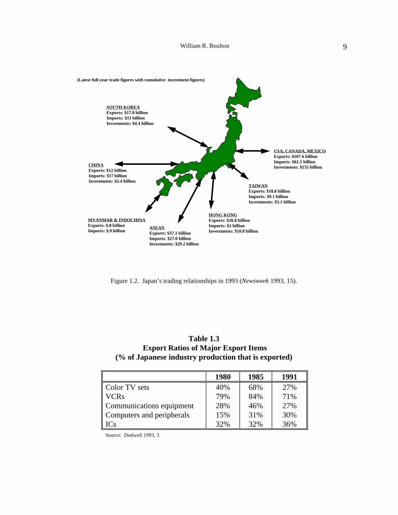
William R. Boulton 9
Figure 1.2. Japan’s trading relationships in 1993 (Newsweek 1993, 15).
Source: Dodwell 1993, 3
SOUTH KOREAExports: $17.8 billionImports: $11 billionInvestments: $4.4 billion
CHINAExports: $12 billionImports: $17 billionInvestments: $3.4 billion
USA, CANADA, MEXICOExports: $107.6 billionImports: $61.5 billionInvestments: $155 billion
TAIWANExports: $18.8 billionImports: $9.1 billionInvestments: $3.1 billion
HONG KONGExports: $20.8 billionImports: $2 billionInvestments: $10.8 billion
ASEANExports: $37.1 billionImports: $27.8 billionInvestments: $29.2 billion
MYANMAR & INDOCHINAExports: $.8 billionImports: $.9 billion
(Latest full-year trade figures with cumulative investment figures)
Table 1.3 Export Ratios of Major Export Items
(% of Japanese industry production that is exported)
1980 1985 1991Color TV setsVCRsCommunications equipmentComputers and peripheralsICs
40%79%28%15%32%
68%84%46%31%32%
27%71%27%30%36%

1. Microelectronics in Japan10
are continuing to move their production facilities overseas (Fig. 1.3). Of 400 overseasproduction bases owned by Japanese electronics makers, 60% are for consumer electronicsplants and 40% for industrial products. The major shift in facilities began in 1985 with amove into Southeast Asia.
Figure 1.3. The movement of Japanese production facilities offshore (William R. Boulton & Assoc.).
The largest number of Japan's Asian plants are located in the Association of SoutheastAsian Nations (ASEAN) nations of Malaysia, Singapore, Thailand, and most recently,Indonesia. Japan’s move to ASEAN countries is a result of its need to restructure globaloperations in light of declining production advantages in Japan, the yen's appreciation,trade friction, and unification of regional markets. These plants provide low- and medium-priced electronics products and components. Of ¥136 billion in consumer electronics goodsimported by Japan in 1991, 86% came from Asia, 8% from the United States, and 5% fromEurope. A number of Japanese companies continued to expand plants in Southeast Asiaduring 1993; however, the investment priority was shifting to China. After having investeda total of nearly $30 billion in Malaysia, for example, Japanese firms invested only $1.5billion in 1992. The number of Japanese investment applications fell from 46 to 35 for theJanuary to April periods of 1992 and 1993, respectively. Japanese investments inSingapore remained high, with nearly $3.5 billion invested in 1993 (Newsweek 1993, 15).
As shown in Table 1.4, of 241 Japanese consumer electronics plants located offshore in1992, 128 were located in Asia, 47 in Europe, 44 in North America, and 22 elsewhere inthe world. Of 168 industrial electronics plants located offshore, 75 plants were in Asia, 38in Europe, 48 in North America, and 7 elsewhere.
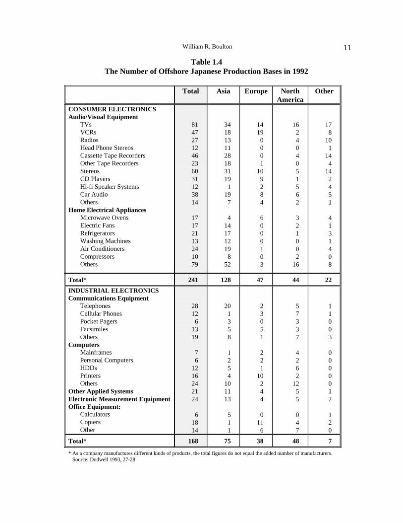
William R. Boulton 11
Table 1.4The Number of Offshore Japanese Production Bases in 1992
Total Asia Europe NorthAmerica
Other
CONSUMER ELECTRONICSAudio/Visual Equipment
TVsVCRsRadiosHead Phone StereosCassette Tape RecordersOther Tape RecordersStereosCD PlayersHi-fi Speaker SystemsCar AudioOthers
Home Electrical AppliancesMicrowave OvensElectric FansRefrigeratorsWashing MachinesAir ConditionersCompressorsOthers
8147271246236031123814
17172113241079
34181311281831191
197
4141712198
52
14190001
109284
6000103
162 40 40 51562
321002
16
178
101
144
142451
4131408
Total* 241 128 47 44 22
INDUSTRIAL ELECTRONICSCommunications Equipment
TelephonesCellular PhonesPocket PagersFacsimilesOthers
ComputersMainframesPersonal ComputersHDDsPrintersOthers
Other Applied SystemsElectronic Measurement EquipmentOffice Equipment:
CalculatorsCopiersOther
28126
1319
76
1216242124
61814
201358
1254
101113
511
23051
221
10244
0116
57337
4262
1255
047
11003
0000012
120
Total* 168 75 38 48 7
* As a company manufactures different kinds of products, the total figures do not equal the added number of manufacturers. Source: Dodwell 1993, 27-28
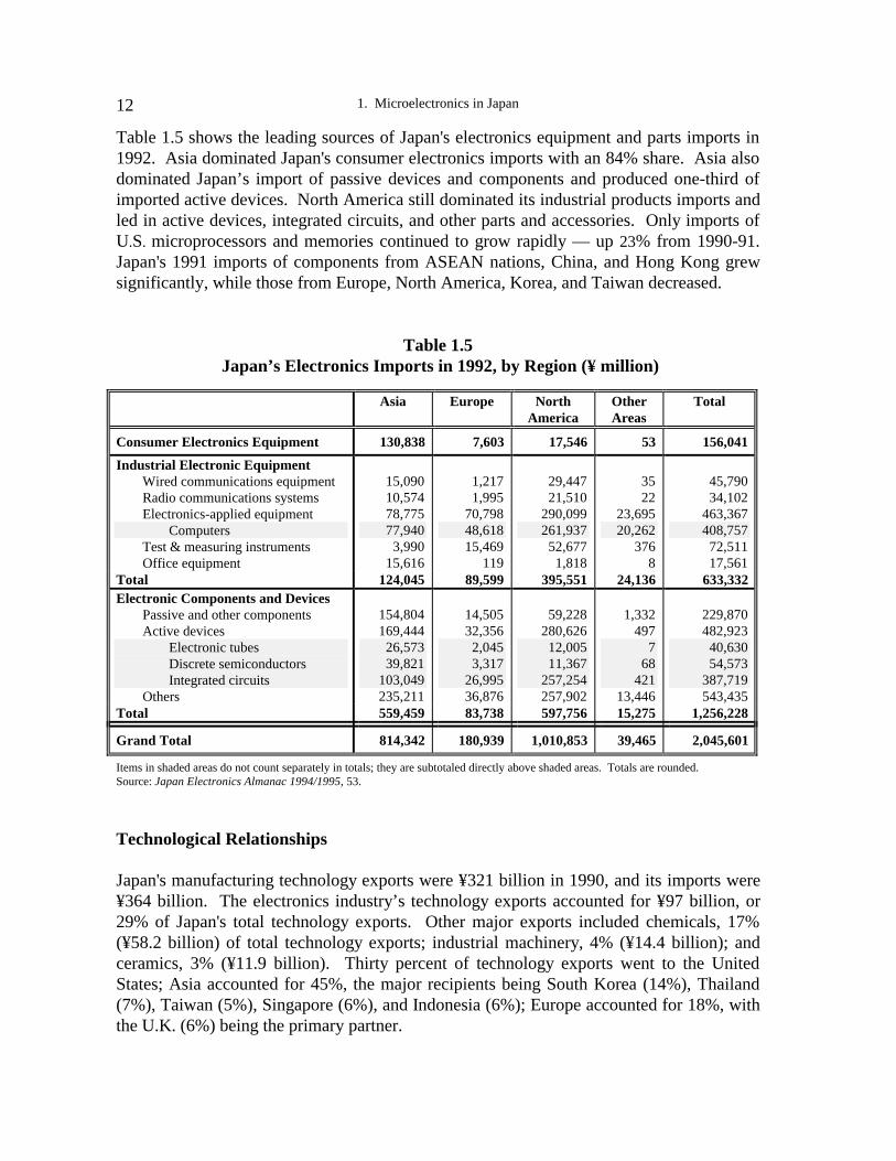
1. Microelectronics in Japan12
Table 1.5 shows the leading sources of Japan's electronics equipment and parts imports in1992. Asia dominated Japan's consumer electronics imports with an 84% share. Asia alsodominated Japan’s import of passive devices and components and produced one-third ofimported active devices. North America still dominated its industrial products imports andled in active devices, integrated circuits, and other parts and accessories. Only imports ofU.S. microprocessors and memories continued to grow rapidly — up 23% from 1990-91.Japan's 1991 imports of components from ASEAN nations, China, and Hong Kong grewsignificantly, while those from Europe, North America, Korea, and Taiwan decreased.
Table 1.5 Japan’s Electronics Imports in 1992, by Region (¥ million)
Asia Europe NorthAmerica
OtherAreas
Total
Consumer Electronics Equipment 130,838 7,603 17,546 53 156,041
Industrial Electronic EquipmentWired communications equipmentRadio communications systemsElectronics-applied equipment
ComputersTest & measuring instrumentsOffice equipment
15,09010,57478,77577,940 3,99015,616
1,2171,995
70,79848,61815,469 119
29,44721,510
290,099261,93752,677 1,818
35 22
23,69520,262 376
8
45,79034,102
463,367408,757 72,51117,561
Total 124,045 89,599 395,551 24,136 633,332Electronic Components and Devices
Passive and other componentsActive devices
Electronic tubesDiscrete semiconductorsIntegrated circuits
Others
154,804169,44426,57339,821
103,049235,211
14,50532,3562,0453,317
26,99536,876
59,228280,62612,00511,367
257,254257,902
1,332497
768
42113,446
229,870482,92340,63054,573
387,719 543,435
Total 559,459 83,738 597,756 15,275 1,256,228
Grand Total 814,342 180,939 1,010,853 39,465 2,045,601
Items in shaded areas do not count separately in totals; they are subtotaled directly above shaded areas. Totals are rounded.Source: Japan Electronics Almanac 1994/1995, 53.
Technological Relationships
Japan's manufacturing technology exports were ¥321 billion in 1990, and its imports were¥364 billion. The electronics industry’s technology exports accounted for ¥97 billion, or29% of Japan's total technology exports. Other major exports included chemicals, 17%(¥58.2 billion) of total technology exports; industrial machinery, 4% (¥14.4 billion); andceramics, 3% (¥11.9 billion). Thirty percent of technology exports went to the UnitedStates; Asia accounted for 45%, the major recipients being South Korea (14%), Thailand(7%), Taiwan (5%), Singapore (6%), and Indonesia (6%); Europe accounted for 18%, withthe U.K. (6%) being the primary partner.
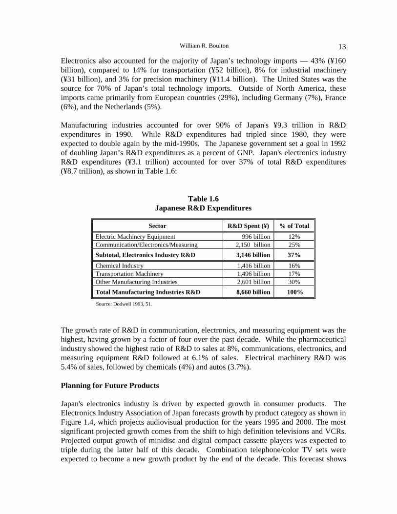
William R. Boulton 13
Electronics also accounted for the majority of Japan’s technology imports — 43% (¥160billion), compared to 14% for transportation (¥52 billion), 8% for industrial machinery(¥31 billion), and 3% for precision machinery (¥11.4 billion). The United States was thesource for 70% of Japan’s total technology imports. Outside of North America, theseimports came primarily from European countries (29%), including Germany (7%), France(6%), and the Netherlands (5%).
Manufacturing industries accounted for over 90% of Japan's ¥9.3 trillion in R&Dexpenditures in 1990. While R&D expenditures had tripled since 1980, they wereexpected to double again by the mid-1990s. The Japanese government set a goal in 1992of doubling Japan’s R&D expenditures as a percent of GNP. Japan's electronics industryR&D expenditures (¥3.1 trillion) accounted for over 37% of total R&D expenditures(¥8.7 trillion), as shown in Table 1.6:
Table 1.6Japanese R&D Expenditures
Source: Dodwell 1993, 51.
The growth rate of R&D in communication, electronics, and measuring equipment was thehighest, having grown by a factor of four over the past decade. While the pharmaceuticalindustry showed the highest ratio of R&D to sales at 8%, communications, electronics, andmeasuring equipment R&D followed at 6.1% of sales. Electrical machinery R&D was5.4% of sales, followed by chemicals (4%) and autos (3.7%).
Planning for Future Products
Japan's electronics industry is driven by expected growth in consumer products. TheElectronics Industry Association of Japan forecasts growth by product category as shown inFigure 1.4, which projects audiovisual production for the years 1995 and 2000. The mostsignificant projected growth comes from the shift to high definition televisions and VCRs.Projected output growth of minidisc and digital compact cassette players was expected totriple during the latter half of this decade. Combination telephone/color TV sets wereexpected to become a new growth product by the end of the decade. This forecast shows
Sector R&D Spent (¥) % of Total
Electric Machinery Equipment 996 billion 12%Communication/Electronics/Measuring 2,150 billion 25%
Subtotal, Electronics Industry R&D 3,146 billion 37%
Chemical Industry 1,416 billion 16%Transportation Machinery 1,496 billion 17%Other Manufacturing Industries 2,601 billion 30%
Total Manufacturing Industries R&D 8,660 billion 100%

1. Microelectronics in Japan14
very little that is totally new; most categories show development of next-generation modelsof products currently on the market. This type of industry projection provides theroadmaps for most Japanese companies as they develop plans for future products. Suchroadmaps help to identify the technologies that will be needed to produce the cominggenerations of products.
Number of Units
Figure 1.4. Japanese forecast of audiovisual production in 1995 and 2000 (Electronics Industry Association of Japan).
Forecasts for growth in computer-related products to 1995 are shown in Figure 1.5. Thehighest volume of production is expected at the low-priced end of the product spectrum.High-volume desktop computers put few constraints on product size but are differentiated
8,100
120,000
1,087,700
16,000
41,600
88,999
5,100
9,000
0
0
2,835,000
9,400
500,000
161,300
72,500
121,500
301,000
120,000
107,000
13,800
0 500,000 1,000,000 1,500,000 2,000,000 2,500,000 3,000,000
Color TVs
CD players for car use
Digital audio tapedecks
High Definition VCRs
HDTV
Portable Mini Discs
Stereo sets withMD/DCC
Telephones withColor TV
Information terminalsfor home use
Compact optical discs
20001995

William R. Boulton 15
by advanced functions. In contrast, notebook computers and personal digital assistants willpush the limits of product miniaturization. (Notebook computers have allowed newcompetition to enter the industry from outside Japan and the United States.)
Thousand Units
Figure 1.5. Number of computer-related systems worldwide (BPA, Dataquest).
Supporting Technologies
Japan's heavy emphasis on the electronics industry has lead it to become a major player inthe production and export of electronic components. In 1992, 52% of electronicscomponents were active components (electron tubes 8%, discrete semiconductors 9%, andintegrated circuits 35%); 15% were passive components such as capacitors, resistors, andinductors; and 31% were other electronic parts (mechanical parts 14%, and audio parts7%). Total production of electronic components was valued at ¥8.8 trillion in 1991, anincrease of 6% over the previous year. The growth rate 1986 to 1991 was 10% per annum.Active components production totaled ¥4.6 trillion in 1991, up 6% over 1990.
Passive component production totaled ¥4.3 trillion, up over 5% from 1990. The highestgrowth areas were discrete semiconductors, passive devices and parts such as connectors,switches, relays, and PCBs, growing at over 7% in 1991. Japan was the largestsemiconductor market in the world, accounting for 39% of 1991 sales, compared to 28%for the United States, 18% for Western Europe, and 15% for the rest of the world. Asshown in Table 1.7, while electronic device sales were down in 1992, they were forecast tocome back again in 1993.
6683
891
3218
631
332
122
17
2
78393
15126
14070
1395
425
217
20
3
39874
1583
1 10 100 1000 10000 100000
Desk PC
Top-end PC
Notebook
Laptop
Workstation
Mini
Mid-range
Mainframe
Supercomputer
1995
1990
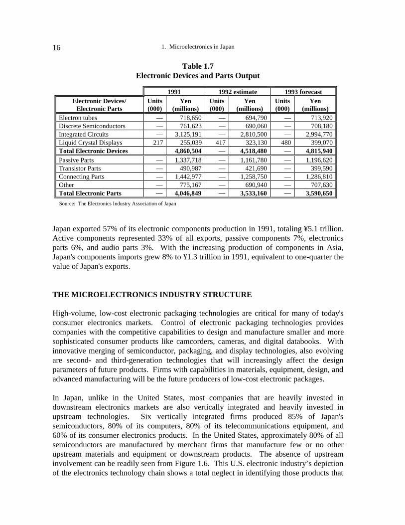
1. Microelectronics in Japan16
Table 1.7Electronic Devices and Parts Output
Source: The Electronics Industry Association of Japan
Japan exported 57% of its electronic components production in 1991, totaling ¥5.1 trillion.Active components represented 33% of all exports, passive components 7%, electronicsparts 6%, and audio parts 3%. With the increasing production of components in Asia,Japan's components imports grew 8% to ¥1.3 trillion in 1991, equivalent to one-quarter thevalue of Japan's exports.
THE MICROELECTRONICS INDUSTRY STRUCTURE
High-volume, low-cost electronic packaging technologies are critical for many of today'sconsumer electronics markets. Control of electronic packaging technologies providescompanies with the competitive capabilities to design and manufacture smaller and moresophisticated consumer products like camcorders, cameras, and digital databooks. Withinnovative merging of semiconductor, packaging, and display technologies, also evolvingare second- and third-generation technologies that will increasingly affect the designparameters of future products. Firms with capabilities in materials, equipment, design, andadvanced manufacturing will be the future producers of low-cost electronic packages.
In Japan, unlike in the United States, most companies that are heavily invested indownstream electronics markets are also vertically integrated and heavily invested inupstream technologies. Six vertically integrated firms produced 85% of Japan'ssemiconductors, 80% of its computers, 80% of its telecommunications equipment, and60% of its consumer electronics products. In the United States, approximately 80% of allsemiconductors are manufactured by merchant firms that manufacture few or no otherupstream materials and equipment or downstream products. The absence of upstreaminvolvement can be readily seen from Figure 1.6. This U.S. electronic industry’s depictionof the electronics technology chain shows a total neglect in identifying those products that
1991 1992 estimate 1993 forecastElectronic Devices/
Electronic PartsUnits(000)
Yen(millions)
Units(000)
Yen(millions)
Units(000)
Yen(millions)
Electron tubes — 718,650 — 694,790 — 713,920Discrete Semiconductors — 761,623 — 690,060 — 708,180Integrated Circuits — 3,125,191 — 2,810,500 — 2,994,770Liquid Crystal Displays 217 255,039 417 323,130 480 399,070Total Electronic Devices 4,860,504 — 4,518,480 — 4,815,940Passive Parts — 1,337,718 — 1,161,780 — 1,196,620Transistor Parts — 490,987 — 421,690 — 399,590Connecting Parts — 1,442,977 — 1,258,750 — 1,286,810Other — 775,167 — 690,940 — 707,630Total Electronic Parts — 4,046,849 — 3,533,160 — 3,590,650
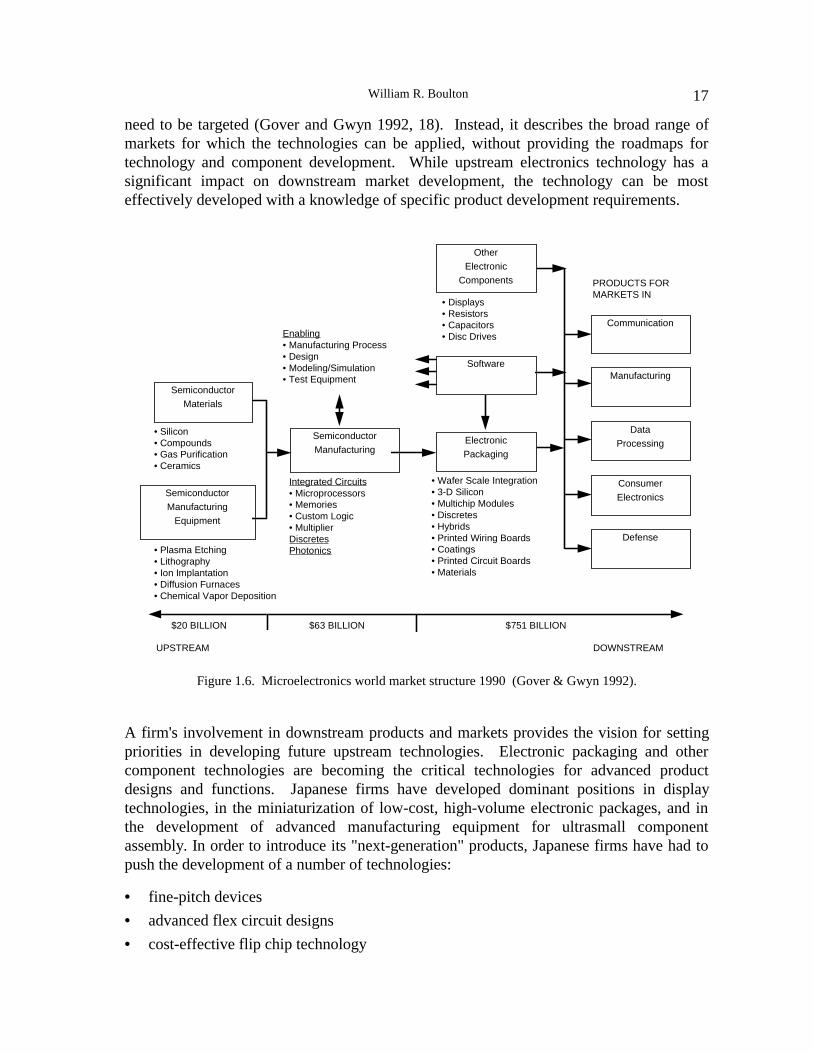
William R. Boulton 17
need to be targeted (Gover and Gwyn 1992, 18). Instead, it describes the broad range ofmarkets for which the technologies can be applied, without providing the roadmaps fortechnology and component development. While upstream electronics technology has asignificant impact on downstream market development, the technology can be mosteffectively developed with a knowledge of specific product development requirements.
Figure 1.6. Microelectronics world market structure 1990 (Gover & Gwyn 1992).
A firm's involvement in downstream products and markets provides the vision for settingpriorities in developing future upstream technologies. Electronic packaging and othercomponent technologies are becoming the critical technologies for advanced productdesigns and functions. Japanese firms have developed dominant positions in displaytechnologies, in the miniaturization of low-cost, high-volume electronic packages, and inthe development of advanced manufacturing equipment for ultrasmall componentassembly. In order to introduce its "next-generation" products, Japanese firms have had topush the development of a number of technologies:
• fine-pitch devices
• advanced flex circuit designs
• cost-effective flip chip technology
Consumer
Electronics
Defense
Data
Processing
Manufacturing
Communication
Semiconductor
Manufacturing
Semiconductor
Materials
Electronic
Packaging
Software
Other
Electronic
Components
Semiconductor
Manufacturing
Equipment
• Silicon• Compounds• Gas Purification• Ceramics
• Plasma Etching• Lithography• Ion Implantation• Diffusion Furnaces• Chemical Vapor Deposition
Integrated Circuits• Microprocessors• Memories• Custom Logic• MultiplierDiscretesPhotonics
• Wafer Scale Integration• 3-D Silicon• Multichip Modules• Discretes• Hybrids• Printed Wiring Boards• Coatings• Printed Circuit Boards• Materials
• Displays• Resistors• Capacitors• Disc DrivesEnabling
• Manufacturing Process• Design• Modeling/Simulation• Test Equipment
UPSTREAM DOWNSTREAM
$20 BILLION $63 BILLION $751 BILLION
PRODUCTS FOR MARKETS IN
1. Microelectronics in Japan18
• cost-effective high-density printed circuit boards
• cost-effective connector technology
• advanced flat panel display technology
• small passive components
• small, low-cost package assembly equipment
• high-speed pick and place equipment for ultrasmall components
These developments now provide Japanese firms with the ability to either design-in greaterfunctionality and performance for any given size product, or to reduce the size or cost ofproducts at any given level of functionality or performance. These "intermediate" packagingcapabilities are expected to provide much of the value added for future electronic productsfrom supercomputers to cameras. In fact, Sony argues that 65% of a product's value addedcomes from key component and device contributions, as compared to only 12% coming fromfinal assembly operations. Therefore, some Japanese firms are reducing dependence onsuppliers for key components as a strategy to improve financial performance. To focusdevelopment efforts in these high-value-added "intermediate" device markets, firms need avision of new product concepts or next-generation product developments.
Sony's historical success is based on a strategy of developing key components to support newproduct developments such as the transistor radio in 1955, the Trinitron in 1968, the Betamaxin 1975, the Walkman in 1979, the CD player in 1982, and the 8 mm camcorder in 1985.Sony's introduction of the Trinitron color television was dependent upon the development ofits single electron gun with three electron beams and an aperture grill. After eight years ofdevelopment, Sony's technological breakthrough was considered the next generation beyondthe shadow mask developed by RCA. Its Trinitron technology continues to provide Sonywith a basic technology for use in advanced high definition television applications. Sony alsodeveloped the charge-coupled device (CCD) as an image-sensing device. After two years ofbasic research, Sony took five years to produce the first small CCD camera for use in theindustrial market; it took five more years to develop the mass production technology requiredto enter the consumer market. Miniaturization of the video camera gave Sony a dominantposition in the 8 mm video camera market.
Sharp has used a similar key device development strategy. It introduced the firstcommercial application of a LCD in an electronic calculator in 1973. Since then, it haspioneered the application of LCDs in Japanese word processors and PCs in 1986, thedevelopment of the world's first 14-inch color thin-film-transfer (TFT) LCD panel in 1988,and the development of LCD video projectors in 1989. Sharp's Hi-8 LCD ViewCam,introduced in 1992, was the world's first camcorder with a 4-inch color TFT LCD monitor.In 1993, Sharp's ViewCam surpassed both Matsushita and JVC products to take secondplace in the video camera market. Sony now plans a similar LCD camcorder to respond toSharp's innovation. Ability to take the lead in critical component technologies is vital todeveloping market leadership.
William R. Boulton 19
In support of next-generation product development and miniaturization goals, the Japaneseelectronics industry is investing in upstream technologies. In 1992 Lloyd Thorndyke, CEOof DataMax, found that electronic packaging technologies of Japan's supercomputermakers were highly advanced. He commented on this in his report:
I was told that the Japanese super computer companies overtook U.S. companiesin super computer packaging five years ago, and that now the lead isinsurmountable. I tend to agree, but for a different reason. The newertechnologies require increasingly greater capital and tooling funding to enterproduction. However, most U.S. super computer companies are relatively small,have low volumes, and limited capital money (1993, 31).
With their heavy commitment to consumer electronics products, Japanese firms havecreated a tremendous demand for upstream electronic technologies, including DRAMmemory chips and many intermediate electronic component and parts technologies.Growing domination of these intermediate component and packaging technologies,including video display technology, provides competitive advantages for future productdevelopments. For example, advanced display technology, integrating both display andpackaging technologies, is expected to pull the development of other microelectronicstechnology into new consumer product applications ranging from hand-held computers tohigh definition television sets.
These conclusions are neither new nor surprising. The Council on Competitivenessreported (1991, 35) that the United States was losing badly or had already lost importantelectronic technologies in display materials, ceramics for electronics, electronic packagingmaterials, gallium arsenide materials, silicon materials, integrated circuit fabrication andtest equipment, microelectronics memory chips, multichip packaging systems, printedcircuit board technology, electroluminescent displays, plasma displays, vacuum fluorescentdisplays, and optical information storage. The Computer Systems Policy Project,composed of the major U.S. computer manufacturers, had come to a similar conclusion in1990, determining that the United States was behind in displays, manufacturingtechnology, ultralarge-scale integrated (ULSI) circuit fabrication equipment and facilities,microelectronics, and electronics packaging. These studies identified six areas as needingspecial attention: optoelectronics, electronic packaging, electronics and semiconductormaterials, display technology, ULSI fabrication equipment, and memory chips. It wasestimated that these six technologies would represent a world market worth of over$100 billion by the year 2000. What is more important, it is expected that whoeverdominates these areas of technology will also dominate the world market for electronicsproducts that is expected to exceed $2 trillion in revenues.
It was clearly evident to the JTEC panel that Japanese companies do not intend to givetheir competitive advantages away. Recently, Sony has limited the number of outsiderswho visit its operations, for fear of losing proprietary information. In cases where outsidersare allowed to visit Sony, they are shown production technology that the company isalready selling to outside customers. The same is true with Matsushita, the
1. Microelectronics in Japan20
world leader in semiconductor insertion equipment, where advanced equipment developedin-house is used for several years before being made available on the open market. Asproduct life cycles continue to shorten, six-month or one-year delays in product availabilitycan mean the difference between substantial profits and significant losses over the shortlife of a product. The component requisition problems are not political issues but rathercompetitiveness issues. Pragmatic business executives are not likely to sell their advancedmicroelectronics technologies or equipment if doing so creates competitors in criticaldownstream markets. Even U.S. semiconductor firms stopped selling components todownstream calculator assemblers once they realized the potential for profit in producingcalculators themselves. As Texas Instrument's chairman Patrick Haggerty reflected (1976),"TI's biggest mistake may have been in not integrating forward into portable radios in theearly 1950s." It was the development of portable radios that gave Sony its first majorconsumer market success.
REFERENCES
Computer Systems Policy Project. 1990. Perspectives: Success Factors in Critical Technologies.
Council on Competitiveness. 1991 (July). Gaining New Ground: Technology Priorities forAmerica’s Future.
Dataquest Incorporated and Quick, Finan and Associates. 1988. The Drive for Dominance:Strategic Options for Japan’s Semiconductor Industry.
Dempa Publications. 1993. Japan Electronics Almanac 1993/1994. Tokyo.
Dempa Publications. 1994. Japan Electronics Almanac 1994/1995. Tokyo.
Dodwell Marketing Consultants. 1993. The Structure of the Japanese Electronics Industry.Tokyo.
Gover, James E., and Charles W. Gwyn. 1992. Strengthening the US Microelectronics Industry byConsortia. Albuquerque, NM: Sandia National Laboratories.
Haggerty, Patrick. 1976. Personal interview with the author.
IEEE-USA Technologies Activities Council. 1989. Workshop on Creation of Government/IndustryPartnerships (February 13-14).
Microelectronics and Computer Technology Corporation and Sandia National Laboratory(MCC/Sandia). 1993. Industrial Competitiveness in the Balance: A Net TechnicalAssessment of North American vs. Offshore Electronics Packaging Technology. (U.S.Department of Energy Contract #AD-3474.)
National Advisory Committee on Semiconductors. 1991 (February). Toward a NationalSemiconductor Strategy: Regaining Markets in High-Volume Electronics.
National Advisory Committee on Semiconductors. 1992 (February). Attaining Preeminence inSemiconductors: Third Annual Report to the President and the Congress. Arlington, Virginia.
Newsweek (Asian edition). 1993 (November 15). “The Coming Eclipse of Greater Japan.”: 15.
Thorndyke, Lloyd M. 1993. “Supercomputer Packaging Technologies Compared.” SIB, 18 Feb.
21
CHAPTER 2
BUILDING THE ELECTRONIC INDUSTRY'S ROADMAPS
William R. Boulton
JTEC panelists found a strong consistency among the electronics firms they visited: all thefirms had clear visions or roadmaps for their research and development activities and hadcommitted resources to ensure that they achieve targeted results. The overarching visiondriving Japan's electronics industry is that of achieving market success through developingappealing, high-quality, low-cost consumer goods — ahead of the competition. Specificsof the vision include improving performance, quality, and portability of consumerelectronics products. Such visions help Japanese companies define in detail the roadmapsthey will follow to develop new and improved electronic packaging technologies.
DIMENSIONS OF PRODUCT DEVELOPMENT IN JAPAN
Companies with clear product development visions know what types of investments arerequired to maintain their market positions. As life cycles of new product generationsbecome shorter, companies can ill afford to delay their product development activities.Product development has therefore become the centerpiece of today's competitivestrategies. Being first to market for next-generation products is what makes companies likeIntel and Microsoft successful. Japanese companies have long shared a competitive vision.Sony's Akio Morita explained this in a speech to the Keidanren (1992):
In pursuit of the goal to "overtake and outrun the Western industries," Japanesemanufacturers have invested all possible resources into technology development,product development, productivity improvement and quality control, and, all of asudden, we have found that a broad range of Japanese products including cars,electronics and machine tools boasts astonishingly competitive strength in theworld market. High-quality, high-performance Japanese products are relativelyinexpensive against those of the same level offered by European and Americancompetitors. Consequently, Japanese products have outsold the competition andbrought success to us in the market.

2. Building the Electronic Industry’s Roadmaps22
Quality, Cost, and Delivery
Japan's competitive objectives in consumer electronics have been clear: lower prices withhigher quality and performance. But as product life cycles continue to shorten, speed ofproduct development has also become a critical factor for success. Since the mid-1980s,Japanese companies have coined the acronym QCD (quality, cost, delivery) for theircompetitive strategy. As shown in Figure 2.1, quality, cost, and delivery time to markethave measurable market share implications. According to Boston-based Strategic PlanningInstitute's PIMS (profit improvement through market share) analysis (1982), firms with alow-price, high-quality position relative to competitors have typically gained 1.1% marketshare per year. In contrast, firms with a high-price, low-quality position relative tocompetition have on average lost 0.7% market share per year. Thus firms that cancontinuously reduce product costs and improve product quality can annually gain nearly2.0% in market share from less aggressive competitors. However, with shorter product lifecycles, firms have less time to make incremental improvements before next-generationproducts are introduced.
New Product Introductions
High
PRICE
Low
Low High
QUALITY
Gain 1.1%Market Share
Per Year
Lose .7% Market Share
Per Year
Gain 50% Market Shareif First to Market
Figure 2.1. Strategic objectives for product development (©William R. Boulton, 1993).
First to Market
Also, as Figure 2.1 shows, the "first-to-market" company is typically able to attain a 50%market share. As long as product leaders continue to stay ahead in developments, they canmaintain a dominant share of the market; fast followers might hold a 25% market share,but late entrants seldom achieve over 10% of the market. For example, Sony continued tohold 49.1% of the Japanese CD player market in 1992, Matsushita held a 27.6% share, and
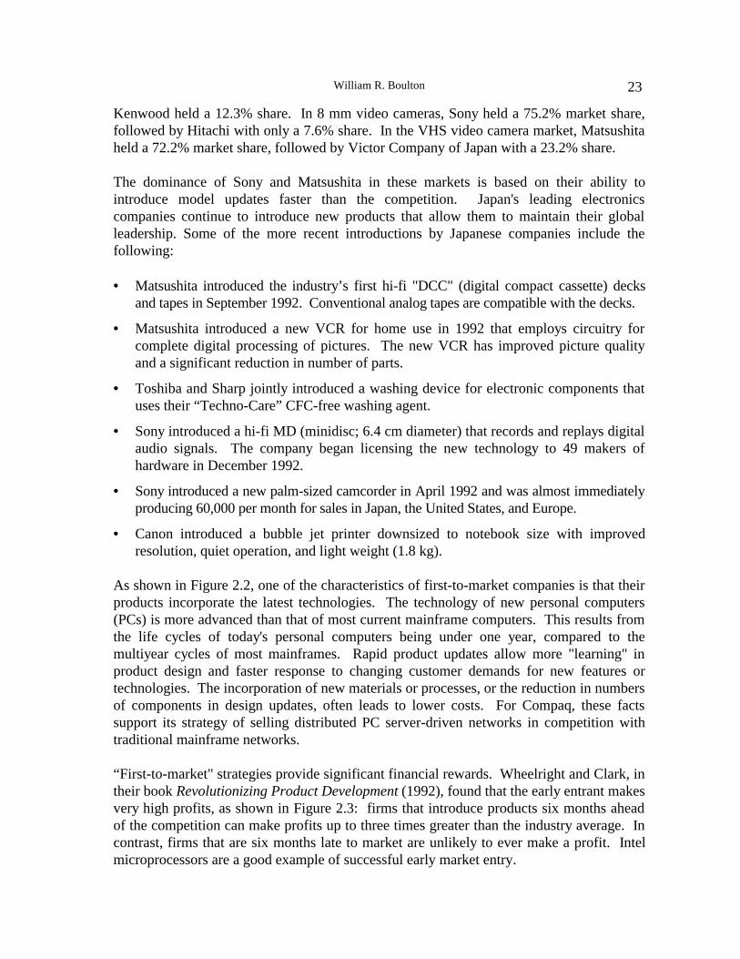
William R. Boulton 23
Kenwood held a 12.3% share. In 8 mm video cameras, Sony held a 75.2% market share,followed by Hitachi with only a 7.6% share. In the VHS video camera market, Matsushitaheld a 72.2% market share, followed by Victor Company of Japan with a 23.2% share.
The dominance of Sony and Matsushita in these markets is based on their ability tointroduce model updates faster than the competition. Japan's leading electronicscompanies continue to introduce new products that allow them to maintain their globalleadership. Some of the more recent introductions by Japanese companies include thefollowing:
• Matsushita introduced the industry’s first hi-fi "DCC" (digital compact cassette) decksand tapes in September 1992. Conventional analog tapes are compatible with the decks.
• Matsushita introduced a new VCR for home use in 1992 that employs circuitry forcomplete digital processing of pictures. The new VCR has improved picture qualityand a significant reduction in number of parts.
• Toshiba and Sharp jointly introduced a washing device for electronic components thatuses their “Techno-Care” CFC-free washing agent.
• Sony introduced a hi-fi MD (minidisc; 6.4 cm diameter) that records and replays digitalaudio signals. The company began licensing the new technology to 49 makers ofhardware in December 1992.
• Sony introduced a new palm-sized camcorder in April 1992 and was almost immediatelyproducing 60,000 per month for sales in Japan, the United States, and Europe.
• Canon introduced a bubble jet printer downsized to notebook size with improvedresolution, quiet operation, and light weight (1.8 kg).
As shown in Figure 2.2, one of the characteristics of first-to-market companies is that theirproducts incorporate the latest technologies. The technology of new personal computers(PCs) is more advanced than that of most current mainframe computers. This results fromthe life cycles of today's personal computers being under one year, compared to themultiyear cycles of most mainframes. Rapid product updates allow more "learning" inproduct design and faster response to changing customer demands for new features ortechnologies. The incorporation of new materials or processes, or the reduction in numbersof components in design updates, often leads to lower costs. For Compaq, these factssupport its strategy of selling distributed PC server-driven networks in competition withtraditional mainframe networks.
“First-to-market" strategies provide significant financial rewards. Wheelright and Clark, intheir book Revolutionizing Product Development (1992), found that the early entrant makesvery high profits, as shown in Figure 2.3: firms that introduce products six months aheadof the competition can make profits up to three times greater than the industry average. Incontrast, firms that are six months late to market are unlikely to ever make a profit. Intelmicroprocessors are a good example of successful early market entry.
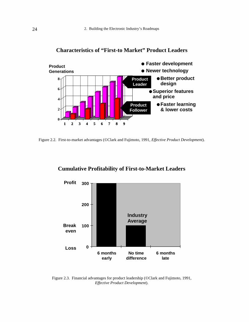
2. Building the Electronic Industry’s Roadmaps24
Characteristics of “First-to Market” Product Leaders
Faster development Newer technology
Better productdesign
Superior featuresand price
Faster learning& lower costs
1 2 3 4 5 6 7 8 90
2
4
6
8
1 2 3 4 5 6 7 8 9
ProductLeader
ProductFollower
ProductGenerations
Figure 2.2. First-to-market advantages (©Clark and Fujimoto, 1991, Effective Product Development).
Cumulative Profitability of First-to-Market Leaders
0
100
200
300
6 monthsearly
No timedifference
6 monthslate
0
100
200
300
6 monthsearly
No timedifference
6 monthslate
Profit
Breakeven
Loss
IndustryAverageIndustryAverage
Figure 2.3. Financial advantages for product leadership (©Clark and Fujimoto, 1991,Effective Product Development).

William R. Boulton 25
Table 2.1 shows recent financial performances of Japan's key electronics firms. Sharp, regardedas the most innovative company in Japan today, shows income levels that surpass companieswith sales three times as great. In 1993, Sharp introduced the 8 mm ViewCam, a low-pricedminidisc CD player, a high-performance washing machine, and an efficient refrigerator.
Table 2.11993 First-Half Performance of Major Japanese Electronics Companies
(% change over previous year first half)
n.m.= no meaning; Source: Nikkei Electronics
Sony’s Leadership With Vision
The JTEC panel's visit to Sony provided an important insight into the use of productdevelopment roadmaps in Japan. The whole team spent one full day at Sony, and somemembers spent a second day visiting Sony's advanced production facilities. Sony has beena product leader in Japan since it introduced the first "pocket-sized" transistor radio in1955. Sony is well known for being one of the most creative and innovative companies inJapan. Akio Morita, the company's chairman, has not relied on market research to decideon product development and to this day does little such research. According to Morita,"You Americans worry too much about market research. The market research is all in myhead! You see, we create markets."
Sony's type of entrepreneurial activity is seldom characteristic of large bureaucratic firmslike NEC, Mitsubishi, or Hitachi; product vision is at the highest levels of the Sonyorganization. The project manager for each of Sony's new product development teams hasbeen either Dr. Ibuka, Mr. Morita, or Mr. Ohga, the corporation's successive chairmen andpresidents. Sony’s current president Ohga was responsible for the minidisc development.Teruaki Aoki, Sony's senior general manager, explained (1989, 5):
I believe one of the most important elements that led us to success was the factthat our top management, Dr. Ibuka, Mr. Morita, and Mr. Iwama, who wereenthusiastic engineers as well as businessmen themselves, were able to present aclear target for research and development in the form of a product idea.
Parent Company Sales Operating Income Ordinary Income
Company Yen(millions)
%Change
Yen(millions)
%Change
Yen(millions)
%Change
Sony
Sharp
Matsushita
Hitachi
Toshiba
NEC
Fujitsu
852,607
575,246
2,147,827
1,932,236
1,535,712
1,332,363
995,298
-0.6
-1.4
-6.4
1.9
1.2
-2.2
-14.1
2,008
11,980
11,711
14,374
5,618
11,127
-6,356
-94.5
-23.7
-57.1
-40.2
-70.6
-40.8
n.m.
16,849
20,177
29,694
29,863
22,419
7,135
-13,793
+25.2
3.5
1.4
1.6
1.5
0.5
-1.4
2. Building the Electronic Industry’s Roadmaps26
Sony’s chief executives have provided their organization with the vision, direction, andresources needed to accomplish technological breakthroughs. The concept of the SonyWalkman, for example, originated when Sony's past chairman, Masaru Ibuka, brought aheavy tape recorder and ear phones into Akio Morita's office one day to listen to music. Itwas hard to walk around the office wearing headphones tied to the large tape deck. Moritathen suggested the need for a more portable unit and asked his staff to make a smallexperimental cassette player with light, comfortable headphones. But the Walkman,introduced in 1979, was not quickly accepted by his own organization. According toMorita (Range 1982, 18),
When we developed the first Walkman, a lot of our salespeople said a smallmachine like that would not sell — especially since it had no recording capability.But I had a hunch it would sell. I said, "Well, a car tape deck doesn't record,either." They were still unenthusiastic. So I said that if we did not sell 100,000sets by the end of the year, I would give up my chairmanship of Sony.
The Walkman sold over 4.5 million units by 1982, and Morita remained as chairman.
Sony's original pocket-sized radio took four years to develop and required R&D expensesthat amounted to 12% of sales. The Trinitron color TV took eight years to develop at anaccumulated R&D cost that amounted to 19% of sales. The CCD (charge-coupled device)development required for the 8 mm video camera took thirteen years and cost $200million. With the continued growth of the company, these project managementresponsibilities once held by senior management have now been passed to the "group-level" general managers.
The vision of portable consumer products has been very successful for Sony, leading to theintroduction of such products as the portable TV, CD player, and 8 mm video camera.Successful development is credited to clear management policies such as the following(Aoki 1989, 14): (1) clear product targets given by top management; (2) focused R&Dunder the strong leadership of top management; (3) intensive R&D for productiontechnology; and (4) transferring many engineers from the research center to the pilot plantand transferring the same engineers from the pilot to production — the transfer ofengineers smoothes the transition from development to production.
The Vision of Miniaturization
Sony’s continued success has required more than product innovations. In addition tocreating markets, Sony has maintained its market share vis-à-vis competitors likeMatsushita, JVC, and Sanyo through timely development of next-generation products.Sony's vision of next-generation products has been that they should be half the price andone-third the weight or size of current products. Sony has maintained its market leadershipwith successful product line expansions and new product developments based on thisvision. The long-term trend in product development can be depicted as shown in Figure 2.4.
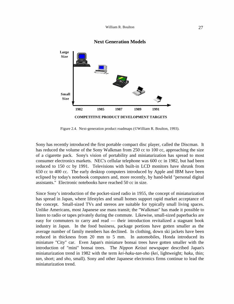
William R. Boulton 27
Next Generation Models
COMPETITIVE PRODUCT DEVELOPMENT TARGETS
LargeSize
SmallSize
1982 1985 1987 1989 1991
Figure 2.4. Next-generation product roadmaps (©William R. Boulton, 1993).
Sony has recently introduced the first portable compact disc player, called the Discman. Ithas reduced the volume of the Sony Walkman from 250 cc to 100 cc, approaching the sizeof a cigarette pack. Sony's vision of portability and miniaturization has spread to mostconsumer electronics markets. NEC's cellular telephone was 600 cc in 1982, but had beenreduced to 150 cc by 1991. Televisions with built-in LCD monitors have shrunk from650 cc to 400 cc. The early desktop computers introduced by Apple and IBM have beeneclipsed by today's notebook computers and, more recently, by hand-held "personal digitalassistants." Electronic notebooks have reached 50 cc in size.
Since Sony’s introduction of the pocket-sized radio in 1955, the concept of miniaturizationhas spread in Japan, where lifestyles and small homes support rapid market acceptance ofthe concept. Small-sized TVs and stereos are suitable for typically small living spaces.Unlike Americans, most Japanese use mass transit; the "Walkman" has made it possible tolisten to radio or tapes privately during the commute. Likewise, small-sized paperbacks areeasy for commuters to carry and read — their introduction revitalized a stagnant bookindustry in Japan. In the food business, package portions have gotten smaller as theaverage number of family members has declined. In clothing, down ski jackets have beenreduced in thickness from 20 mm to 5 mm. In automobiles, Honda introduced itsminiature "City" car. Even Japan's miniature bonsai trees have gotten smaller with theintroduction of "mini" bonsai trees. The Nippon Keizai newspaper described Japan'sminiaturization trend in 1982 with the term kei-haku-tan-sho (kei, lightweight; haku, thin;tan, short; and sho, small). Sony and other Japanese electronics firms continue to lead theminiaturization trend.
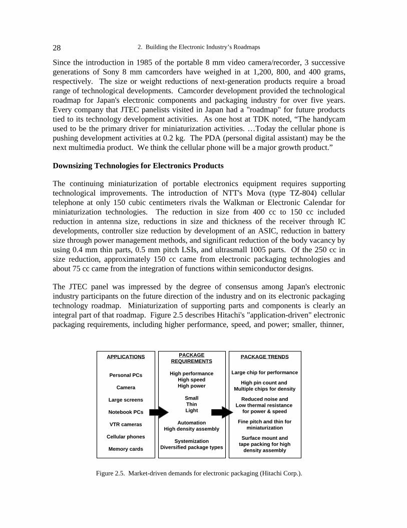
2. Building the Electronic Industry’s Roadmaps28
Since the introduction in 1985 of the portable 8 mm video camera/recorder, 3 successivegenerations of Sony 8 mm camcorders have weighed in at 1,200, 800, and 400 grams,respectively. The size or weight reductions of next-generation products require a broadrange of technological developments. Camcorder development provided the technologicalroadmap for Japan's electronic components and packaging industry for over five years.Every company that JTEC panelists visited in Japan had a "roadmap" for future productstied to its technology development activities. As one host at TDK noted, “The handycamused to be the primary driver for miniaturization activities. …Today the cellular phone ispushing development activities at 0.2 kg. The PDA (personal digital assistant) may be thenext multimedia product. We think the cellular phone will be a major growth product.”
Downsizing Technologies for Electronics Products
The continuing miniaturization of portable electronics equipment requires supportingtechnological improvements. The introduction of NTT's Mova (type TZ-804) cellulartelephone at only 150 cubic centimeters rivals the Walkman or Electronic Calendar forminiaturization technologies. The reduction in size from 400 cc to 150 cc includedreduction in antenna size, reductions in size and thickness of the receiver through ICdevelopments, controller size reduction by development of an ASIC, reduction in batterysize through power management methods, and significant reduction of the body vacancy byusing 0.4 mm thin parts, 0.5 mm pitch LSIs, and ultrasmall 1005 parts. Of the 250 cc insize reduction, approximately 150 cc came from electronic packaging technologies andabout 75 cc came from the integration of functions within semiconductor designs.
The JTEC panel was impressed by the degree of consensus among Japan's electronicindustry participants on the future direction of the industry and on its electronic packagingtechnology roadmap. Miniaturization of supporting parts and components is clearly anintegral part of that roadmap. Figure 2.5 describes Hitachi's "application-driven" electronicpackaging requirements, including higher performance, speed, and power; smaller, thinner,
PACKAGEREQUIREMENTS
High performanceHigh speedHigh power
SmallThinLight
AutomationHigh density assembly
SystemizationDiversified package types
APPLICATIONS
Personal PCs
Camera
Large screens
Notebook PCs
VTR cameras
Cellular phones
Memory cards
PACKAGE TRENDS
Large chip for performance
High pin count and Multiple chips for density
Reduced noise andLow thermal resistance
for power & speed
Fine pitch and thin forminiaturization
Surface mount andtape packing for high
density assembly
Figure 2.5. Market-driven demands for electronic packaging (Hitachi Corp.).

William R. Boulton 29
and lighter packages; higher density assembly and advanced automation; and multiplepackage types and integrated multichip module systems.
As another example of a roadmap used by the electronics industry in Japan, Nitto Denko, aleading "packaging technology" firm, provided Table 2.2 to the panel. Although this tablewas produced by the U.S. Semiconductor Industry Association, Nitto Denko follows a verysimilar roadmap. The key characteristics of this roadmap include finer pattern width andpin pitch, and multichip modules.
The primary technologies used for downsizing of electronic packaging include continuedminiaturization of surface mount devices (SMD), increased integration of circuitpackaging, and reduced printed circuit board (PCB) dimensions.
Table 2.2.Packaging Technology for the 21st Century
Source: U.S. Semiconductor Industry Association.
1992 1994 1996 1998 2000Pattern Widths (mm)
0.5 0.4 0.3 0.25 0.2 Integrated density DRAM
SRAM16M 64M 256M 4M 16M 64M
Size logicDRAM
250 400 600 700132 200 320 400
Frequency off chipon chip
60 100 175 200120 200 350 400
Power microcomputerminicomputermainframe
3 4 4 410 15 30 3515 30 40 100
Bonding Pitch
wire bondTABflip chip
100 70 50 limit100 70 50200 200 150 100
Package Smaller/Thinner
thicknesspin countpin pitchpower
1.4 1 bare chip<80 <208 MCM-L0.3-0.5 0.3-0.5<1W <2W
High pin count pin countpin pitchpower
200-300 300-400 bare chip0.5 0.4 MCM-L<2-5W 5-10W
Area array pin countpad pitchpower
200-300 500-600 750 20000.2-1.5 0.2-1.0 0.15-0.8 0.1-0.5<2-5W 5-10W 10-15W 40W
Application workstation
portable
1 chip, PGA MCM (4-8 chip) 8-16 chips1 chip/ surface mount COB MCM (area array and thin types) COG

2. Building the Electronic Industry’s Roadmaps30
Surface Mount Devices. With the development of surface mount technology (SMT),electronic parts such as transistors and capacitors no longer need leadwires. This reducessize requirements as well as potential quality problems related to bending, inserting wiresinto holes on PCBs, soldering, and cutting inserted wires. In the mid-1980s, new 3216-type (3.2 mm by 1.6 mm parts) resistors and condensers began to replace the traditionalleadwire type parts for use in surface mount applications. These new parts only requireplacement and soldering functions.
Since the introduction of surface mount parts and application equipment, surface mounttechnologies have been used widely in the design and manufacture of portable consumerelectronics such as calculators, radio-cassette decks, cameras, and video cameras.According to a survey of the Japan Printed Circuits Association, calculators used 100%SMD for assembly. Products using over 90% SMD in assembly included radio-cassettedecks, still cameras, and video cameras. There has been rapid growth in the application ofSMD to industrial products, with larger computers using nearly 90% SMD, and computerperipherals, telephones, and electric parts using around 80%.
The continued application of SMT has allowed parts sizes to be continuously downsized,reaching 1608-type (1.6 mm by 0.8 mm) parts in 1990 and 1005-type (1.0 mm by 0.5 mm)in 1993. This is a reduction to one-third the initial length and one-tenth of the area ofearlier parts. As explained to the JTEC panel by our TDK hosts,
When we talk about things that are small in Japan, we call them like a grain of rice.Rice grains are 5.09 mm. Sesame seeds average 3.72 mm in diameter. In the early1980s, the average size of capacitors and resistors were 3.2 mm by 1.6 mm. Thatwas the same time that the next generation was introduced, but the 2.0 mm by1.25 mm capacitors and resistors didn't become the standard until about 1990. Our1608 multilayer ceramic capacitor of 1.6 mm by 0.8 mm was introduced in the late1980s. We introduced the 1.25 mm by 0.6 mm versions around 1990, but don'texpect it to become the standard until around the mid-1990s. Our smallest chip is1005, or 1.0 mm by 0.5 mm. It is smaller than a poppy seed, which is 1.18 mm.People cannot handle this size chip. We need machines to mount these small chips.
The weight of 1005 is so light that the tension of solder exerts a force greater thanthe weight of the component. So 1005 creates new structural problems. Today,there are four machine makers that produce machines for 1005, but users are notyet buying them. These machines were introduced at the same time as the 1005components through close coordination. The next generation may be 0.65 by 0.3.Many people are thinking about the solder problem and are trying to developreliable solder materials.
Critical to vendor introduction of new SMT devices was the simultaneous developmentand introduction of assembly equipment that could handle the new components. Withvendors supplying both the components and the equipment, the time required for customersto utilize the new technology has been reduced. Sharp, for example, designed new 1005

William R. Boulton 31
components into the PCB of its new 8 mm ViewCam. When asked if there were anyproblems introducing the new component technology, the plant manager said, "No, we justasked our suppliers to help us."
Integrated Circuit (IC) Packaging. New IC packaging technologies have increasingly beendeveloped for SMT applications. For example, 100-pin QFP (quad flat packages) with0.65 mm lead pitch were introduced in the mid-1980s. In the 1990s, these are beingreplaced with 120-pin TQFP (thin quad flat packages) with 0.5 mm lead pitch and 1.4 mmthickness. Two-hundred-pin VSQFP (very small quad flat packages) with 0.3 mm leadpitch are expected to be introduced in 1994. Toshiba recently developed TAB (tapeautomated bonding) equipment for 520-pin, 0.2 mm lead-pitch packages. The newequipment utilizes CCD image sensors to scan outer leads using 400,000 pixel imagedensity. There are also many approaches using multichip module designs to improvedensity for product miniaturization.
Oki Electric Industry Company, a major supplier of electronic components, was especiallyhelpful in providing roadmaps for logic LSI packaging, memory LSI packaging, and tapecarrier packages. The Oki roadmap for logic LSI packaging is shown in Table 2.3.
Table 2.3Logic LSI Package Roadmap
* Thin, thin quad flat packages. Source: Oki Electric Industry Co.
Year (CY) 1990 1993 1996 1999 2002
Gate density 200K 300K 500K 1M 2M
LSI Max. chip size 15 mm 15 mm 17.5 mm 20 mm 25 mm
Chip Max. power 1.5W 2W 3W 5W 10W
Trend Max. speed 50MHz 150MHz 300MHz 500MHz 500MHz
Max. pin count 250 350 500 750 1000
High
Pin Count
QFP
208
(40x0.65)
(28x0.5)
304
(40x0.5)
176
(20x0.4)
256
(28x0.4)
344
(28x0.3)
504
(40x0.3)
PackageC-PGA
(BPGA)
401
(40x1.778)
526
(32x1.27)
750
(36x1.27)
1000
(40x1.27)
Technology Thin Pkg.
(Pkg. Height)
TQFP
(1.2 mm)
100 144
(14x0.5)(20x0.5)
TTQFP*
(0.8-0.5 mm)
216
(24x0.4)
176
(14x0.4)
344
(28x0.3)
240
(20x0.3)
296
(24x0.3)
High Power Cu lead
frame
QFP with
heat spreader
QFP with
cool module
High Speed Singlelayer lead
frame
QFP withmultilayer
PCB

2. Building the Electronic Industry’s Roadmaps32
Printed Circuit Boards. By 1991, single-sided rigid PCBs represented about 14.4% of theapplications. One-third of the applications were double-sided rigid PCB applications. Butto improve density, multilayer PCBs are growing rapidly, having doubled their applicationin four years. Rigid boards with three to four layers accounted for 20.3% of theapplications in 1991, with five-to-nine-layer boards accounting for 14.4%, and ten-layerboards accounting for 3.1%.
With the increasing fluidity of product designs, there has also been growth in flexible printedcircuits (PCs). One-sided flex circuits represented about 3% of applications in 1991, withmultilayer circuits accounting for 5.6% of applications. New technologies for flexible PCsinclude flex-rigid and copper clad laminate (CCL) for adhesiveless two-layer structures thatenable high-temperature soldering at 350°C for small electronic products. Chip on flex-board(COF) has become a key downsizing technology with IC chips wire-bonded directly to theflexible PC. This is used in NTT's most recent "wristwatch-style" pager. Camera makersincorporate the most extensive use of flex-board technology in their miniaturization efforts.
Matsushita provides an interesting example of video camera miniaturization efforts. Oneof the measures used to assess the efficiency of design in PCB layout is the number ofcomponents per square centimeter. Matsushita recently described the improvements in thedesign and layout of its video camera between 1990 and 1993; Table 2.4 shows theincreasing density of components used on the "camera" and "video" boards.
Table 2.4Matsushita Video Camera Board Designs
Source: Nikkei Electronics 1993, 6.
The following conclusions can be drawn from Matsushita’s data:
• integration of functions has reduced the number of components by half
Si
(6/90)
S5
(5/91)
S9
(91)
TI
(4/92)
CS1
(4/93)
PCB size
(sq. cm)
Video bd.
Camera bd.
Total size
113
98
211
103
87
190
108
62
170
(one
board)
122
(one
board)
75
Number of
components
Video bd.
Camera bd.
Total #
1100
700
1800
1050
650
1700
1050
400
1450 1433 930
Average # of
components
per sq. cm.
Video bd.
Camera bd.
Overall
9.7
7.1
8.5
10.2
7.5
8.9
9.7
6.5
8.5 11.7 13.0
Highest density 11 12 12 14 16
William R. Boulton 33
• increase in number of components per square centimeter (8.5 to 13) has allowed a 50%improvement in density
• combined increases in functional integration and component density have allowed a65% reduction in PCB size
• between 1990 and 1993, the most compact video camera was also reduced in weight by200 grams and in size by 100 cubic centimeters
Developing Next-Generation Technologies
Japanese consumer electronics producers continue to work on evolutionary technologicaldevelopments that allow them to introduce new or next-generation products. Pioneeringtechnical developments announced in 1992 included the following:
• a 256M bit DRAM memory cell — the world's smallest size (NEC)
• a 16M-bit NAND flash memory — only 2.3 times the size of 4M-bit models (Toshiba)
• a new STN-type LCD that delivers 40% higher light transmission for use in notebook-type PCs (Toshiba)
• an artificial retina chip that recognizes images in 200 microseconds and characters in3 microseconds. The new chip, 100 to 10,000 times faster than old processors, will beapplied to robots and remote sensors (Mitsubishi)
• a 9:16-aspect CRT display that includes a converter for HDTV applications (Mitsubishi)
• an orange-color semiconductor laser for use in high-density optical disks, displays, andlaser pointers (Sanyo)
• a high-temperature semiconductor laser for 780-nanometer applications such as next-generation laser beam printers that are small, lightweight, quiet, and high speed (Sharp)
Japanese roadmaps for future product development all stress the continued design oflighter, thinner, and smaller products, with development of enabling packaging andmanufacturing technologies to support such products. At the time of the JTEC team’s visitthe trend had already seen the shift from "desk top" to "laptop" to "notebook" to "palm top"electronics products. The chip packages were shifting from dual inline packages (DIP), tosmall outline packages (SOP) and quad flat packages (QFP), to chip on board (COB) andtape automated bonding (TAB) components. An increase in bare chip applications isexpected as a transition to multichip modules. At the same time, chip components havebeen reduced in size from 3216 (3.2 mm by 1.6 mm) to 2125 (2.1 mm by 2.5 mm) to 1608(1.6 mm by 0.8 mm) to 1005 (1.0 mm by 0.5 mm) in a period of under six years.According to TDK managers, the next generation is likely to be 0.65 mm by 0.3 mm. Newtechnologies for manufacturing are critical to support these miniaturization efforts asproduction equipment shifts from insertion machines to surface mount machines capable ofhandling a greater variety of devices.
2. Building the Electronic Industry’s Roadmaps34
CONCLUSIONS
Reflecting on the successes of the Japanese consumer electronics business, the JTEC panelfinds that having a clear vision of new or next-generation products and their supportingtechnological developments is a critical factor. Gearing for specific end-products byproceeding along a well-defined road for developing components within specific size andperformance parameters has allowed for efficient use of resources and rapid developmenttimeframes. There is little doubt in the minds of panel members that the Japanesecompanies they visited will be successful in their development efforts, particularly sincemembers of Japan’s electronics industry cooperate to overcome technical barriers.
The ability to develop and introduce next-generation products is based on a broad range oftechnological and manufacturing capabilities that has shifted in importance over the pastdecades. Reductions in product life cycles and component sizes have placedmanufacturing technologies at the center of the competitive equation today. With theincreased miniaturization of products and their components and parts, equipmentnonavailability can become a barrier to rapid introduction of new products andcomponents. Updated process technology is one of the underlying forces highlighted inthis report that is critical to future success in electronic packaging and consumerelectronics.
While companies like Sony have been product innovators, introducing a series of newproducts that have created new markets, the majority of Japanese suppliers have beensuccessful by concentrating their efforts on developing succeeding generations ofinnovative feeder products. U.S. innovations have been lost over time to foreigncompetitors who quickly have exploited the technology to advance their product strategies.There must be a vision of next-generation developments for product leadership to bemaintained over time.
REFERENCES
Aoki, Teruaki. 1989. Sony’s Way: R&D Strategy. Sony’s Innovation and Management Series,Vol. 3. Sony Corp.
Morita, Akio. 1992. “ ‘Japanese-style Management’ in Peril: Why the West Denounces thePractice of ‘High Quality at Low Price’.” Speech to the Keidanren (February).
Nikkei Electronics 1993 (August):6.
Strategic Planning Institute. 1982. Publication # 28.
Range, Peter Ross. 1982. “Playboy Interview: Akio Morita.” Playboy, August, page 18.
Wheelright, Steven, and Kim Clark. 1992. Revolutionizing Product Development. New York:The Free Press.
35
CHAPTER 3
JAPAN'S TECHNOLOGY AND MANUFACTURING
INFRASTRUCTURE
William R. BoultonEugene S. MeieranRao R. Tummala
The JTEC panel found that, after four decades of development in electronics andmanufacturing technologies, Japanese electronics companies are leaders in thedevelopment, support, and management of complex, low-cost packaging and assemblytechnologies used in the production of a broad range of consumer electronics products.The electronics industry's suppliers provide basic materials and equipment required forelectronic packaging applications. Panelists concluded that some Japanese firms could beleading U.S. competitors by as much as a decade in these areas. Japan’s technology andmanufacturing infrastructure is an integral part of its microelectronics industry’s success.
OVERVIEW OF JAPAN’S TECHNOLOGY INFRASTRUCTURE
A 1993 study by the U.S. Department of Commerce's Technology Administration(DOC/TA 1993) identified both the national and local levels of Japan's technologyinfrastructure. At all levels, the technology infrastructures in the United States and Japanhave a number of similarities:
• industry associations provide forums for industry people to meet
• professional societies publish journals and sponsor technical meetings and standardscommittees
• R&D consortia allow companies to jointly develop and manage technology
3. Japan’s Technology and Manufacturing Infrastructure36
• public and private groups diffuse technology to small- and medium-sized companies
• consulting firms provide technical information to companies
• networks (such as regional networks of engineers) facilitate communication amongprofessionals
• education and training programs transfer knowledge and help organizations be betterreceivers of technology
• government organizations, such as the National Technical Information Service in theUnited States and the Japan Information Center for Science and Technology,disseminate technical information
• technical databases make up-to-date information widely accessible
Despite these similarities, there are many differences between the U.S. and Japanesetechnology infrastructures. According to the DOC report, industry associations in Japanare more deeply involved in technology development and management than those in theUnited States. In Japan it is large companies, rather than consulting firms as in the UnitedStates, that play a major role in transferring technology within the industry. Japan also hasextensive experience with utilizing consortia as a mechanism for developing technology-sharing activities across companies and industries. At the regional level, Japan has 172kohsetsushi centers that provide technological services to small- and medium-sizedcompanies that lack strong keiretsu (company groupings) ties. Prefectural laboratories areinvolved in research, development, and transfer of advanced technologies. Close proximityof engineering societies in Japan allow for extensive personal networks, and likewise,personalized supplier-customer relations provide for close technical relationships. Incontrast, the United States relies more heavily on computer networks like Bitnet andInternet. Finally, Japan relies more heavily than does the United States on education andtraining within companies, on institutional training programs, and on individual trainingprograms outside companies.
Japanese Government Support For High-Technology Industries
Support of high-technology industries by the Government of Japan (GOJ) is at least fourdecades old. In 1952, Japan's Agency of Industrial Science and Technology (AIST) wasreorganized under the newly established Ministry of International Trade and Industry(MITI) to coordinate Japan's technological developments. Manufacturing and electronictechnology developments were the responsibility of the Mechanical EngineeringLaboratory (MEL) and the Electro-Technical Laboratory (ETL). Two major laws werepassed — the Machinery Industry Law in 1956 and the Electronics Industry Law in 1957— to promote experimental research and initial production, and also to promote industrialrationalization of machine tools and electronic technologies. Under these laws, subsidiesfor technology R&D were provided, along with special loans and tax incentives for firmsthat developed or used advanced production technologies. By 1980, Japan had become theworld leader in machine tools for component production and in robots for assembly.

William R. Boulton, Eugene S. Meieran, Rao R. Tummala 37
In Japan, about one-fifth of technology R&D funding comes from government sources.(By comparison, about half of all U.S. technology R&D spending comes from governmentsources.) Government R&D policy in Japan supports the rationale that basic researchshould be carried out by universities and national laboratories, and much of Japan'sgovernment R&D funds support basic research. In addition, however, the government hasattempted to stimulate industrial R&D in areas that are important for the future of thenation's industrial technology base. The government's role has been primarily that ofproviding strategic leadership and of acting as the catalyst for private R&D investment.Japanese capital markets support longer-term investments in technology, training, andother activities that improve a firm's long-term growth potential than do U.S. capitalmarkets (DOC/TA 1993). The GOJ does fund strategic investments that address perceivedneeds for advanced, precompetitive technology in private industry where projects areconsidered too risky in financial or technical terms for private investment.
The GOJ policy to provide leadership and promote private investment for advancedtechnology development has required extensive communication between industry andgovernment in determining R&D priorities in Japan. The lack of antitrust enforcement inJapan has facilitated cooperation and coordination of industry research activities. In anumber of ways, government policies in Japan function to support consensus andinterdependence within the high-technology industries.
JAPAN'S TECHNOLOGY DEVELOPMENT STRATEGY
Japanese culture views technology as a tool for making marketable products. Productiontechnology is central to such a view and has become a clear force in developingcompetitive advantage for Japan's industrial giants, as shown in Figure 3.1. An effectivevision of next-generation products combined with continuous product improvementsprovide the vision for "upstream" developments. Japan's focus on production equipmentand process improvements is directed towards designing for cost and manufacturability:that is, Japan’s focus is on designing processes to improve productivity, increase quality,and decrease cost; designing concurrent engineering methods to speed productintroductions; developing software to implement and improve factory automation; anddevising effective management methods related to all of the above. The following aresome of the JTEC panel's findings regarding technology R&D in Japan:
• Japan uses its patent system to facilitate the transfer of intellectual property ratherthan to protect it. The Japanese patent system is meant to educate, as opposed toprotect an invention as in the U.S. system. Japanese patent applications are madepublic and open to rebuttal by competitors. As a result, it is difficult for a firm toexploit its own technology. There are many examples of Japanese firms flooding amarket with trivial patents around a basic patent for the purpose of forcing the basicpatent owner to cross-license its core technology, in order to gain access to that market.A second strategy is to develop a portfolio of related or similar patents that likewisemake it difficult for a firm to exploit its core technology alone.

3. Japan’s Technology and Manufacturing Infrastructure38
SolveReliabilityProblems
SUPPLIERMATERIALS
ANDPROCESS
DEVELOPMENT
ProductTargets
Design ForLow Cost AndHigh Quality
DESIGN FORLOW COST/
MANUFACTURING
USE PROVENTECHNOLOGIES
AUTOMATEFACTORIES
SolveReliabilityProblems
CORPORATIONMATERIALS
ANDPROCESS
DEVELOPMENTCONSUMERMARKETS
INDUSTRIALMARKETS
ProductPlans For:
I M PROVEDPRODUCTS
NEXTGENERATIONPRODUCTS
NEXTGENERATION
COM PONENTS
SATISFIEDCUSTOMERS
Figure 3.1. Japan’s successful production development strategy.
• Japanese firms appoint a greater number of technically trained managers to head uptheir companies. Past studies show that as many as 75% of the CEOs ofmanufacturing firms have engineering degrees.
• Japanese firms invest heavily in the development of production automationtechnology. Japanese firms concentrate on developing in-house process and equipmenttechnologies that provide competitive capabilities.
• Japanese firms have separate R&D organizations for production technologies.R&D for such activities can account for as much as two-thirds of R&D investments;most of the remaining one-third is for product development. U.S. ratios are reversed.
• Japanese firms seek to identify customer needs as the basis for developing newproducts and setting roadmaps for technological development. In Japan it is productrequirements that drive advanced technology development activities (product pullrather than technology push as in the United States). To keep costs down, Japanesefirms utilize proven technologies that have been tested and can be incrementallyimproved. New technologies are used only when other alternatives will not work.
• Japanese firms make long-term commitments to the development of new products,components, equipment, and technologies. There are numerous examples of Japanesecommitments to long-term developments, such as Sony's 13-year program to introducecharge-coupled device (CCD) image pickup components for the camcorder. One JTECpanelist saw the same presentation he had seen three years earlier, updated to show theprogress that had been made. Development of batteries and ceramics for automobileshas continued since the 1960s and has yet to see a payback. Sharp licensed RCA'sliquid crystal display (LCD) technology and spent nearly a billion dollars over a decadebefore its development efforts were brought to market.

William R. Boulton, Eugene S. Meieran, Rao R. Tummala 39
• Japanese firms use teams with a common vision as the basis for concurrentengineering activities. A dedicated and skilled team approach is standard operatingprocedure in Japan, in contrast to one centered on highly educated individualists as inthe United States. Japanese team members understand the entire systems view of theproduct vision, which results in products that look and function as though they weredesigned by a single person. This team approach is found throughout the industry"food chain." It involves hundreds of vendors, many of which are small familyoperations, and many large parent companies or customers. It is often said that thestrength of Japan’s industrial system comes from this “small family” approach.
• Japanese firms have limited research relationships with universities. There are onlya few examples of strong research relationships between Japanese universities andindustry. Large companies conduct their own basic research or license it from outsideJapan. The dean at Sophia University recently complained that Japanese firms werespending more in U.S. universities than in Japanese universities. In contrast, U.S.universities have contributed heavily to the basic research required by U.S. industry.
• Local government supports industrial research activities. To support developmentactivities within local communities, nearly 160 municipal industrial research institutes(MIRIs) have been established through local industry and municipal governmentcooperation. Their facilities are impressive, with well-equipped research laboratoriesand libraries. One Nagoya MIRI has a staff of 100, including 25 engineering Ph.D.s.They provide consulting, testing, analysis, research, technical information, seminars,and courses for local industry. No comparable facilities exist in the United States.
• Japanese firms conduct parallel development programs for both long- and short-term product improvements. Departments often pursue two to five technologiessimultaneously in order to ensure that they can be ready to introduce next-generationproducts in a timely manner. Corporate research centers typically conduct developmentwork on efforts requiring over five years. Often, research centers are heavily involvedin the development of next-generation products, while divisions make incrementalproduct improvements on an annual basis. In contrast, U.S. research organizations seekfreedom to do independent research without direct application objectives; as a result,U.S. product developments are delayed, and technology transfer is typically difficult.Figure 3.2 illustrates the Japanese parallel development strategies.
As Figure 3.2 shows, Japanese firms have developed a systematic approach to long-term product development. Business units are responsible for ongoing operations andthe competitive improvement required to maintain current market positions. For mostproducts, minor changes are made annually; for products like the Sony Walkman, suchchanges are made every six months or less. Corporate-level product teams areresponsible for development of substantive product improvements before thecompetition. (For Sony, that has meant smaller and smaller camcorders.) Ability toprovide new product innovations depends on a company's development of newcomponent technologies like LCDs or CCDs, which is dependent upon long-termresearch. Corporate level technology research teams are responsible for long-termtechnological developments. The JTEC panel found that most large firms work at all
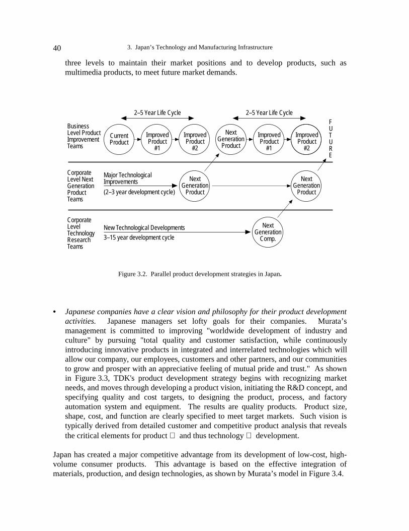
3. Japan’s Technology and Manufacturing Infrastructure40
three levels to maintain their market positions and to develop products, such asmultimedia products, to meet future market demands.
Figure 3.2. Parallel product development strategies in Japan.
• Japanese companies have a clear vision and philosophy for their product developmentactivities. Japanese managers set lofty goals for their companies. Murata’smanagement is committed to improving "worldwide development of industry andculture" by pursuing "total quality and customer satisfaction, while continuouslyintroducing innovative products in integrated and interrelated technologies which willallow our company, our employees, customers and other partners, and our communitiesto grow and prosper with an appreciative feeling of mutual pride and trust." As shownin Figure 3.3, TDK's product development strategy begins with recognizing marketneeds, and moves through developing a product vision, initiating the R&D concept, andspecifying quality and cost targets, to designing the product, process, and factoryautomation system and equipment. The results are quality products. Product size,shape, cost, and function are clearly specified to meet target markets. Such vision istypically derived from detailed customer and competitive product analysis that revealsthe critical elements for product and thus technology development.
Japan has created a major competitive advantage from its development of low-cost, high-volume consumer products. This advantage is based on the effective integration ofmaterials, production, and design technologies, as shown by Murata’s model in Figure 3.4.
Business Level Product Improvement Teams
Corporate Level Next Generation Product Teams
Corporate Level Technology Research Teams
Current Product
Improved Product
#1
Improved Product
#2
Next Generation
ProductImproved Product
#1
Improved Product
#2
Major Technological Improvements(2–3 year development cycle)
FUTURE
New Technological Developments3–15 year development cycle
2–5 Year Life Cycle 2–5 Year Life Cycle
Next Generation
Product
Next Generation
Product
Next Generation
Comp.

William R. Boulton, Eugene S. Meieran, Rao R. Tummala 41
Figure 3.3. TDK’s product development strategy.
Figure 3.4. Japanese passive component strategy (Murata).
The technological imperative of Japan’s integration strategy is "cost comes first." WhileJapan is developing competitive technologies for high-performance products likesupercomputers, it also has the leadership in low-cost, high-volume consumer products likecamcorders, televisions, and stereos. That provides Japanese firms with the uniqueadvantage of having technological capabilities in both high-performance and low-costtechnologies. Low-cost, high-volume products provide the impetus to develop massproduction technologies that reduce production costs while also raising production qualityand volume. Increased demand for product variety has provided further incentives forJapanese firms to develop flexible assembly systems that allow development of lower-
MarketNeed
ProductVision
R&DConcept
Quality/Cost
Target
ProductDesign
Process Design
Equipment/Factory
Automation
QualityProduct
TDK’s PRODUCTDEVELOPMENT
STRATEGY
M a te ria lsT e ch n o lo g y
(C era m ics)
D e sig nT e ch n o lo g y
(E lectro n icM a ch in e ry)
P ro d u ctio nT e ch n o lo g y
(P ro cess)
P ro d u cts
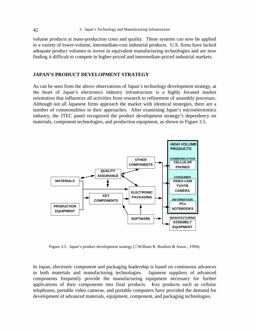
3. Japan’s Technology and Manufacturing Infrastructure42
volume products at mass-production costs and quality. These systems can now be appliedto a variety of lower-volume, intermediate-cost industrial products. U.S. firms have lackedadequate product volumes to invest in equivalent manufacturing technologies and are nowfinding it difficult to compete in higher-priced and intermediate-priced industrial markets.
JAPAN’S PRODUCT DEVELOPMENT STRATEGY
As can be seen from the above observations of Japan’s technology development strategy, atthe heart of Japan’s electronics industry infrastructure is a highly focused marketorientation that influences all activities from research to refinement of assembly processes.Although not all Japanese firms approach the market with identical strategies, there are anumber of commonalities in their approaches. After examining Japan’s microelectronicsindustry, the JTEC panel recognized the product development strategy’s dependency onmaterials, component technologies, and production equipment, as shown in Figure 3.5.
PCsNOTEBOOKS
ASSEMBLYEQUIPMENT
CELLULARPHONES
KEYCOMPONENTS
MATERIALS
ELECTRONICPACKAGING
SOFTWARE
OTHERCOMPONENTS
PRODUCTIONEQUIPMENT
HIGH VOLUMEPRODUCTS
QUALITYASSURANCE
VIDEO CAMTV/VTR
CAMERA
COMMUNICATION
CONSUMER
INFORMATION
MANUFACTURING
Figure 3.5. Japan’s product development strategy (William R. Boulton & Assoc., 1994).
In Japan, electronic component and packaging leadership is based on continuous advancesin both materials and manufacturing technologies. Japanese suppliers of advancedcomponents frequently provide the manufacturing equipment necessary for furtherapplications of their components into final products. Key products such as cellulartelephones, portable video cameras, and portable computers have provided the demand fordevelopment of advanced materials, equipment, component, and packaging technologies.

William R. Boulton, Eugene S. Meieran, Rao R. Tummala 43
Competitive Advantages in Component Technologies
Component technologies provide the greatest opportunities for Japanese companies toapply their manufacturing expertise to competitive advantage, because the mechanical andelectrical components for most consumer products have long life cycles. Sony developedits CCD and Sharp its LCD in the mid-1980s. While external design changes in productcolor, shape, or features may occur every six months for products like Sony’s Walkman orannually for products like Sharp's ViewCam, major improvements in componenttechnologies occur only every three to five years. For example, during a time period thatSony introduced over 160 models of the Walkman, there were only five changes in itsmechanical component "platform."
After developing key component technologies, Japanese companies have been able todesign and introduce a wide range of products based on those technologies. Hugeindustries have evolved from development of components for such products as personalcomputers, VCRs, video disks, and cellular telephones. Sharp, for example, is applyingLCD technology for home entertainment, audio equipment, home appliances, and medicalequipment. Key components with broad applications provide long-term growth potential.Semiconductor and communications technologies have been the basis for many of today'sproduct developments. In essence, these new products have created new market demandsthrough a strategy of "technology push." When Sharp’s president encouraged managers toapply LCD technology to their product lines, he implemented a technology-push strategy.
Competing in Next-Generation Components
Every industry has its own "rules of conduct" and strategies for targeting market segmentsto stimulate market share growth. With regard to high-volume electronic assembly,Japan’s strategy has been to lower costs, reduce size and weight, and improve functionality.Camcorders, cellular telephones, VCRs, stereos, and CD players have all been subjected tothis strategy. These product demands have then generated the roadmaps for componentand packaging development.
Microprocessors are one of the few components that are still controlled by U.S. firms.According to Gordon Moore, CEO of Intel, the complexity of integrated circuit deviceswill roughly double every device generation, one generation lasting about 18 months,resulting in a straight-line on a log scale as shown in Figure 3.6. The semiconductorindustry sees no short-term departure from this trend. As a consequence, feature size andresolution of geometries used in production follow the same trend, with feature sizereductions of about 20% per component generation. At the same time, increased functionalintegration has lead to larger chip sizes, which has required materials development forincreased wafer size and equipment development for handling larger wafers. The projectedcharacteristics of next-generation IC components allow designers to plan for next-generation products.

3. Japan’s Technology and Manufacturing Infrastructure44
Year
101
102
103
104
105
106
107
108
1970 1975 1980 1990 1995 2000
Chip Complexity
Figure 3.6. Moore’s Law of Active Element Density.
Recent Intel advertisements have clearly presented the company's progress in improvingprocessor performance. For example, using Intel's performance computations, thefollowing ratings have been achieved with its most recent microprocessors:
Relative Performance Ratingi486 SX-25 100i486 SX-33 133i486 DX-33 160IntelDX2-50 233IntelDX2-66 290Pentium Processor-60 525Pentium Processor-66 560
By adding increased capability with each component generation, microprocessor designersgive potential customers a broader range of design capabilities. Moore once stated thatwhile he did not know what people will do with all of the transistors being manufactured,he was confident that demand will exist for increased functions, power, and speed that giveadded design options to the innovative users of these advanced components. Indeed,demand continues to grow as new applications are developed for each new componentintroduction or update. In addition to providing next-generation complex instruction setchip (CISC) microprocessors, Intel provides a full range of processors to fit a wide range ofproduct applications from servers to notebook computers. The United States hasdominated the high-end semiconductor device market by continuing such rapiddevelopments.
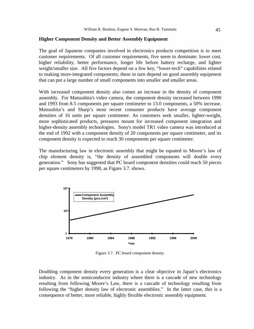
William R. Boulton, Eugene S. Meieran, Rao R. Tummala 45
Higher Component Density and Better Assembly Equipment
The goal of Japanese companies involved in electronics products competition is to meetcustomer requirements. Of all customer requirements, five seem to dominate: lower cost,higher reliability, better performance, longer life before battery recharge, and lighterweight/smaller size. All five factors depend on a few key, “lower-tech” capabilities relatedto making more-integrated components; these in turn depend on good assembly equipmentthat can put a large number of small components into smaller and smaller areas.
With increased component density also comes an increase in the density of componentassembly. For Matsushita's video camera, the component density increased between 1990and 1993 from 8.5 components per square centimeter to 13.0 components, a 50% increase.Matsushita’s and Sharp’s most recent consumer products have average componentdensities of 16 units per square centimeter. As customers seek smaller, lighter-weight,more sophisticated products, pressures mount for increased component integration andhigher-density assembly technologies. Sony's model TR1 video camera was introduced atthe end of 1992 with a component density of 20 components per square centimeter, and itscomponent density is expected to reach 30 components per square centimeter.
The manufacturing law in electronic assembly that might be equated to Moore’s law ofchip element density is, “the density of assembled components will double everygeneration.” Sony has suggested that PC board component densities could reach 50 piecesper square centimeters by 1998, as Figure 3.7. shows.
Year
1
101
102
1976 1980 1984 1988 1992 1996 2000
Component AssemblyDensity (pcs./cm 2)
Figure 3.7. PC board component density.
Doubling component density every generation is a clear objective in Japan’s electronicsindustry. As in the semiconductor industry where there is a cascade of new technologyresulting from following Moore’s Law, there is a cascade of technology resulting fromfollowing the “higher density law of electronic assemblies.” In the latter case, this is aconsequence of better, more reliable, highly flexible electronic assembly equipment.

3. Japan’s Technology and Manufacturing Infrastructure46
New-Technology-Based Innovations Versus Process-Based Improvements
It has repeatedly been stated that U.S. research and development is driven by a technologypush, in contrast to Japanese research and development, which is primarily driven by aproduct or market pull. There are, of course, occasions when the technology is virtuallyindistinguishable from the product driven by the technology; microprocessor technology,for example, is ubiquitous to digital electronics, but when referring to an Intel ‘486 orPentium, it is often the personal computer product that comes to mind. Thus a technologyinnovation can spawn a new product and, at times, spawn a whole new industry.
Indeed, in the past several decades “new technology” has supported the development ofmany new electronics industries. Examples include the personal computer, VCR, CD-ROM, and cellular telephone, satellite communications, neural networks, expert systems,semiconductor memories for electronics, and information-sciences-based products. In thecase of the personal computer, an entire industry that now affects the global economydeveloped from an innovation for making video games available to the home market.
When a new market is created around a new product based on a new technology, marketdemand is created largely by the customers’ interest in the newness of the product. As themarket develops, the technology creator can maintain market advantage by continuouslyenhancing the technology and introducing newer and more improved products in responseto customer demands, as discussed in Chapters 2 and 4. The product enhancementsinitiated by repeated introduction of new technology keep competitors in a continuous stateof playing “catch-up.” If successful, the technology leader captures a major share of themarket long before the competition can respond, and the leader can sustain that position aslong as the product family continues to be improved and meets customer demands. Aspointed out in Chapter 2, Sony and Sharp are two Japanese firms that have market strengthbased on introduction of innovative products.
In general, the United States has long operated under the belief that technology innovationswill, by themselves, sustain industrial growth and market strength. New technology andresulting new products often originate in university or industrial research laboratories. Thebetter and more attractive the technology, the broader the range of product applications isexpected, and the stronger the customer demand for newer and more enhanced productsbased on the technology. The more rapidly the market develops, the greater the advantagefor the technology developer.
In contrast to this U.S. R&D operating scenario, Japan has operated under the belief thatnew technology developments have to be focused on continually upgrading products tomeet customer demands for highest possible quality at lowest possible cost. The leaderstays ahead of the competition by being faster or less expensive in bringing out upgradedproducts. Over time, however, process technology improvements can often be a decidingfactor in whether or how fast product quality can be improved and cost reduced.Depending on the nature of the product and its state of market maturity, an aggressive
William R. Boulton, Eugene S. Meieran, Rao R. Tummala 47
manufacturer can take the lead away from the product or technology innovator and becomea market giant. Matsushita did this in the VCR market, and Compaq appears to be doingthis in the PC market.
The Importance of Process Technology
There is a clear market transition from the stage when an innovative product is firstintroduced, to the stage of continuing development of the product in response to consumerdemands. In the first phase, the consumer is attracted to the product largely because of itsnovelty, and the innovator is temporarily unchallenged in the market. In the second phase,the consumer becomes increasingly cost and quality conscious, and many competitors mayenter the market; then the emphasis on manufacturing technology takes over from theemphasis on new technology.
The camcorder, the cellular telephone, the Walkman, the CD-ROM, and the personalcomputer all appear to be maturing into more manufacturing-process-influenced industries.With the resulting increased competition in the marketplace, there is increased pressure tolower cost, improve performance, make the product easier to use, etc. At this stage,process technologies and component upgrade technologies can easily become moreimportant than the original technology innovations. The market for Dynamic RandomAccess Memory (DRAM) invented by Intel is now dominated by innovative and highlycompetitive manufacturers, predominantly Japanese (Fujitsu, NEC, etc.) or Korean(Samsung, Gold Star, etc.). The market for VCRs, for which the fundamental technologywas invented by Ampex, is now dominated by Matsushita and Sony.
Technology development activities of the Japanese manufacturing leaders are customer-and product-driven. Dominant market position is occupied by suppliers that bestunderstand how to meet and increase market needs. The criteria for success are attention todetail, clear understanding of customer needs, and flawless execution. Clearly, with regardto high-volume electronic assembly, customers demand lower cost, improved functionality,smaller size, and lighter weight, especially for more mobile products. Japanese packaging,component, and process technology development is driven by these parameters.
While it might be reasonably argued that the U.S. “technology push” approach to R&Dproduces more Nobel Prize winners, the Japanese “customer (or product) pull” approach toR&D has produced market leadership for Japan, especially thanks to its emphasis onprocess technology R&D. U.S. automakers were pushed by Japanese competition intolearning how to make cars quality-competitive with those made by the Japanese.Automated electronic assembly factories in the United States, such as SCI and AVEX, arenow as good as any Japanese factory, although many use Japanese-built equipment.However, manufacturing in the electronic assembly and packaging arena has not beentargeted as an area for U.S. attention, as in the case of the automobile industry. Theimplications of this omission may be truly ominous.
3. Japan’s Technology and Manufacturing Infrastructure48
INDUSTRIAL COMPUTERIZATION
Automated Systems
Japan has a long history of using mainframe computers for central processing and controlactivities that facilitate productivity. Japan's computerization blueprint, developed in themid-1960s, was specifically directed at improving productivity. According to MasaruMurai, president of Compaq (Japan), this blueprint has since been implemented.
Prior to the Olympic Games and the introduction of the shinkansen bullet train in 1964,there was no computer-based automation in Japan. Hitachi introduced computerizedticketing systems and scheduling controls for the shinkansen. The steel company Yahatapurchased the 1964 Olympics' mainframe computer to build an automated mill withcomputer-controlled processing. It also bought IBM’s sensor-based 1710 processcomputers. At about the time steel firms started using computers for automated productioncontrol systems, Toyota started using computers to control just-in-time production systems,and banks started using computers for ATM and savings account automation. Today,Japanese electronics companies have fully automated factories. Every aspect ofmanufacturing, from product design to shipping, except maintenance and some limitedassembly activities, is computer-controlled.
Software
In 1985, the International Robotics and Factory Automation Association was formed inJapan for the purpose of developing factory automation software. The objective was todevelop a standard language for use in computer-integrated factories. General Motors’"MAP" protocol was used as the basis for this effort. By 1992, a full-scale integratedfactory was demonstrated at the Japan Exhibition Center in Makuhari Messe, near Tokyo.All equipment makers in Japan had standardized new advanced equipment around "miniMAP," Japan's approach to widespread application of computer-integrated manufacturingconcepts. Mini MAP utilized only four of the seven levels of MAP capability. However,this demonstrated the feasibility of the approach and provided a lower-cost language forequipment makers to apply to advanced manufacturing equipment.
Japanese companies continue to apply productivity-based tools like CAD/CAM/CAEsoftware, to speed the time for product development and production start-up. Sharp's newViewCam utilized full application of CAD/CAM software in the development of theproduct and its manufacturing system.
Information Systems
While Japan may be a leader in automated production and control technologies, it is behindin information network developments. The deregulation of the telecommunicationsindustry has been slow and has limited the availability of advanced communicationsystems. At Hitachi, e-mail systems were available at the time of the JTEC visit, but

William R. Boulton, Eugene S. Meieran, Rao R. Tummala 49
access and use was limited by the absence of a computer-based infrastructure; there wasonly one computer for every eight engineers. At NEC, a corporate-wide e-mail system wasplanned for 1995. Insufficient office space has kept Japanese firms from installingcomputers on every desk. JTEC panelists noticed that most computers were in a locationseparate from offices.
Instead of relying on information systems, Japanese firms continue to rely on human-basedcommunications through teamwork, fax communications, and face-to-face interactions.Because most individuals live within three hours of Tokyo, meetings continue to be thedominant form of communications. The world's major corporations have offices within a45-minute commute from central Tokyo.
Collaborative team-building activities have helped to build Japanese economic strength.Companies like Sony hold monthly meetings between researchers, laboratories, andcorporations to discuss and share research results. As a consequence, results are widelydisseminated. Conferences are used for industrywide problem-solving efforts that spurcontinuous technological improvements. There is little duplication of effort, as progress isregularly shared between industry players. As JTEC panelists visited companies likeHitachi, Oki, Matsushita, TDK, and Nitto Denko, they heard similar descriptions oftechnical problems and found a high level of agreement between competitors as topotential solutions. Widespread industry consensus in Japan was a major panel finding.
Building a national information infrastructure, recently announced as a U.S. objective, wasalso adopted as a national objective by the Japanese government in 1993. As companiesadopt the new vision of an information superhighway, they are expected to invest heavilyin multimedia products. Japan recently established the Hi-Vision Promotion Center, theHi-Vision Promotion Association, and a museum of the Association for Promotion ofHi-Vision, all for the purpose of coordinating and communicating HDTV developments inanticipation of future multimedia and interactive environments. Japan's forecasts for theyear 2000 show HDTV being the number one consumer electronics product of the future.Sony is considered the leader in multimedia technologies and is attempting to positionitself to take advantage of the information superhighway.
ELECTRONICS RESEARCH ACTIVITIES
Japanese electronics firms are investing billions of dollars in R&D activities. As shown inTable 3.1, the top ten electronics firms in Japan invested an average of 7.8% of sales inR&D in 1991. They continue to search for those advanced technologies and componentsthat will assure future competitive advantage in the marketplace.
The recession in Japan affected investment levels only slightly. For example, Matsushita'srevenues fell from ¥7.4 trillion in 1992 to ¥7.0 trillion in 1993, with a drop in profits from¥363 to ¥170 billion; Sony's revenues grew slightly from ¥3.9 to ¥3.95 trillion, but profitsfell from ¥197 billion to ¥80 billion; still, Matsushita's R&D expenditures increased from
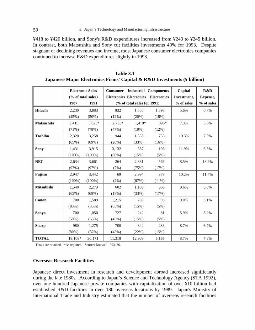
3. Japan’s Technology and Manufacturing Infrastructure50
¥418 to ¥420 billion, and Sony's R&D expenditures increased from ¥240 to ¥245 billion.In contrast, both Matsushita and Sony cut facilities investments 40% for 1993. Despitestagnant or declining revenues and income, most Japanese consumer electronics companiescontinued to increase R&D expenditures slightly in 1993.
Table 3.1Japanese Major Electronics Firms' Capital & R&D Investments (¥ billion)
Totals are rounded. *As reported. Source: Dodwell 1993, 86.
Overseas Research Facilities
Japanese direct investment in research and development abroad increased significantlyduring the late 1980s. According to Japan’s Science and Technology Agency (STA 1992),over one hundred Japanese private companies with capitalization of over ¥10 billion hadestablished R&D facilities in over 180 overseas locations by 1989. Japan's Ministry ofInternational Trade and Industry estimated that the number of overseas research facilities
Electronic Sales
(% of total sales)
1987 1991
Consumer Industrial Components
Electronics Electronics Electronics
(% of total sales for 1991)
Capital
Investment,
% of sales
R&D
Expense,
% of sales
Hitachi 2,230 3,883
(45%) (50%)
932 1,553 1,398
(12%) (20%) (18%)
5.6% 6.7%
Matsushita 3,415 5,825*
(71%) (78%)
2,733* 1,419* 896*
(47%) (19%) (12%)
7.3% 5.6%
Toshiba 2,320 3,258
(65%) (69%)
944 1,558 755
(20%) (33%) (16%)
10.3% 7.0%
Sony 1,431 3,915
(100%) (100%)
3,132 587 196
(80%) (15%) (5%)
11.9% 6.3%
NEC 2,634 3,661
(97%) (97%)
264 2,831 566
(7%) (75%) (17%)
8.5% 18.9%
Fujitsu 2,947 3,442
(100%) (100%)
69 2,994 379
(2%) (87%) (11%)
10.2% 11.4%
Mitsubishi 1,540 2,273
(65%) (68%)
602 1,103 568
(18%) (33%) (17%)
9.6% 5.0%
Canon 700 1,589
(83%) (85%)
1,215 280 93
(65%) (15%) (5%)
9.0% 5.1%
Sanyo 700 1,050
(59%) (65%)
727 242 81
(45%) (15%) (5%)
5.9% 5.2%
Sharp 980 1,275
(80%) (82%)
700 342 233
(45%) (22%) (15%)
8.7% 6.7%
TOTAL 18,108* 30,171 11,318 12,909 5,165 8.7% 7.8%

William R. Boulton, Eugene S. Meieran, Rao R. Tummala 51
owned by Japanese companies increased 86.6% between 1986 and 1989, and during thesame period the number of researchers employed by these facilities more than doubled,from 3,300 to 6,975 (MITI 1991). In 1992, the STA survey reported 117 Japanesemanufacturing companies operating 276 overseas R&D facilities (STA 1992).
The number of Japanese electronics R&D facilities in the United States increased fromabout 22 facilities in 1987 to nearly 110 facilities in 1992. This shift corresponded to thegrowing presence of Japanese goods in the U.S. marketplace. Of 150 Japanese facilities inthe United States in 1993, over 70% were established between 1986 and 1992 (DOC1993, 17). A majority of these facilities focus on computers, computer software,semiconductors, telecommunications, television-audio-radio, and optoelectronics.
In 1992, Sony had fifteen R&D facilities in the United States, Fujitsu had eleven, andMatsushita had nine. In addition to moving development activities closer to their markets,Japanese firms set up these R&D facilities in the United States because they recognized theweakness of basic scientific research activities in Japan. To take advantage of U.S.scientific leadership, Japan established R&D facilities near major U.S. university andindustry technology centers. This was expected to shorten development cycles and allowearly access to new business opportunities (DOC 1993, 23).
Basic Research
In the United States, innovation often comes out of university or industry basic researchactivities. For example, a large number of new concepts and products have come fromsuch institutions as MIT, Stanford, Bell Labs, IBM, Fairchild, Intel, and Texas Instruments.In contrast, Japanese labs visited by the JTEC panel focused primarily on improvingproducts that already had established markets. University and government laboratoryequipment was considered outdated and not as sophisticated as that of corporatelaboratories. Since 1981, Japan's austerity budget had cut finding for governmentlaboratories. Most government-funded laboratories had deteriorated with the budget cutsby the time of the JTEC visits.
Instead of relying on domestic university or government basic research, Japanese firmshave continued to rely heavily on research from U.S. facilities such as MIT's MediaLaboratory. Japanese companies have also continued to establish basic research facilitiesin the United States. In Japan, the best-equipped industrial labs appear narrowly focusedand tightly structured. On the other hand, firms are attempting to improve creativitythrough the development of more "Western"-type incentive programs. Sony and TDKrecently developed reward systems to encourage more innovative research.
Japanese firms are adept at understanding the product opportunities resulting from U.S.research efforts. For example, Apple Computer developed a strategic alliance with SharpCorporation for the manufacture of the new personal digital assistant called Newton. Sharpintroduced its lower-priced version of the Newton nearly four months before Apple wasable to complete the "complex" technical developments of the Newton. As one TDK

3. Japan’s Technology and Manufacturing Infrastructure52
executive explained, "We are very good at making things for our customers, but we do notreally understand what product we should make." However, once they learn what to make,Japanese companies are very fast at product development and market introduction.
In the observation of JTEC panelists, the best Japanese industrial labs are comparable withU.S. labs in the nature and amount of equipment. Japanese technical publications are ofoutstanding quality, but most research is directed at short-term, incremental technicalimprovements. The work has very pragmatic goals — to solve very specific technicalproblems rather than invent new technologies. Panelists did not detect an atmosphere ofgreat excitement in the labs. Still, there are several notable Japanese companies committedto the long-term development of future technologies as well as to shorter-term productdevelopment. Hitachi's research structure, described below, is representative of the broadR&D capabilities of Japan's most influential electronics firms.
HITACHI'S R&D STRUCTURE
The R&D philosophy of Hitachi is that of the company's founder, Namihei Odaira,"Though we cannot live one hundred years, we should be concerned about one thousandyears hence." Hitachi's stated research goal is to perform "long-term, continuous researchto meet social needs and corporate policy in the next decades through development oforiginal science and/or significant patents." Therefore, Hitachi’s advanced and centralresearch laboratories are devoted to the long-term development of new fields of scienceand technology. The following are some examples of Hitachi's ongoing research programs,with their development time frames:
Three to five years
• neural networks on silicon chips that mimic learning
• multimedia offices, where computers have high-resolution screens and hi-fi audio anddouble as video conference terminals
• magnetic levitation trains three times faster than today's fastest traditional trains
Five to ten years
• hand-held computers that obey handwritten or voice commands and exchangeinformation over radio waves
• virtual-reality technology that allows users on a network to meet and interact incomputer-simulated environments
Ten to twenty years
• superconducting chips packing 100 times more data, 10 times the speed of today's chips
• neural computers made of tens of thousands of powerful microprocessors, combiningoptical and electronic circuits and able to learn and reason

William R. Boulton, Eugene S. Meieran, Rao R. Tummala 53
• electronic switches made from a single atom
• translation software for any of the world's languages
• high definition television with thin liquid-crystal or plasma screens > 30” wide
• underground magnetic levitation conveyors linked by software for distribution of goodsin congested cities
• fusion reactors based on the process that fuels the sun
More than 20 years
• biocomputers, whose organic materials can repair themselves like living creatures
• intelligent cities, with homes and offices wired with fiber optics that send voice, image,and computer data, and are run by electronic control centers
Hitachi's allocation of R&D funds is broken down according to general categories inFigure 3.8
8%
16%
76%
Basic Research inLaboratories
Applied Research inLaboratories
Product Development inDivisions
Figure 3.8. Hitachi’s distribution of R&D funds.
Over the years Hitachi has built a strong portfolio of intellectual property assets that it hasused to gain strategic positioning in high-technology markets. Hitachi ranks fourth in totalnumber of U.S. patents granted since 1963, right after IBM, GE, and AT&T. Since 1985,the company has earned more income from licenses than it has paid out; in 1991 it reporteda net profit on technology licensing activities of ¥24.5 billion ($200 million), about 20% ofits operating profits before taxes. Hitachi has twenty patent lawyers on payroll. Thecompany's recent patenting strategy has been to develop a smaller number of patents strongenough to provide negotiating power for cross-licensing arrangements. It does not want tobe left out of new product areas because of patent restriction, and it therefore attempts to
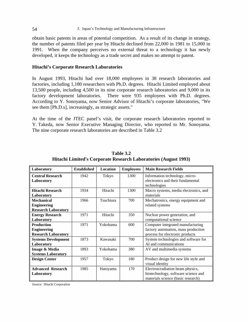
3. Japan’s Technology and Manufacturing Infrastructure54
obtain basic patents in areas of potential competition. As a result of its change in strategy,the number of patents filed per year by Hitachi declined from 22,000 in 1981 to 15,000 in1991. When the company perceives no external threat to a technology it has newlydeveloped, it keeps the technology as a trade secret and makes no attempt to patent.
Hitachi’s Corporate Research Laboratories
In August 1993, Hitachi had over 18,000 employees in 38 research laboratories andfactories, including 1,180 researchers with Ph.D. degrees. Hitachi Limited employed about13,500 people, including 4,500 in its nine corporate research laboratories and 9,000 in itsfactory development laboratories. There were 935 employees with Ph.D. degrees.According to Y. Sonoyama, now Senior Advisor of Hitachi’s corporate laboratories, "Wesee them [Ph.D.s], increasingly, as strategic assets."
At the time of the JTEC panel’s visit, the corporate research laboratories reported toY. Takeda, now Senior Executive Managing Director, who reported to Mr. Sonoyama.The nine corporate research laboratories are described in Table 3.2
Table 3.2Hitachi Limited's Corporate Research Laboratories (August 1993)
Source: Hitachi Corporation
Laboratory Established Location Employees Main Research Fields
Central ResearchLaboratory
1942 Tokyo 1300 Information technology, micro-electronics and their fundamentaltechnologies
Hitachi ResearchLaboratory
1934 Hitachi 1300 Macro systems, media electronics, andmaterials
MechanicalEngineeringResearch Laboratory
1966 Tsuchiura 700 Mechatronics, energy equipment andrelated systems
Energy ResearchLaboratory
1971 Hitachi 350 Nuclear power generation, andcomputational science
ProductionEngineeringResearch Laboratory
1971 Yokohama 600 Computer integrated manufacturingfactory automation, mass productionprocess for electronic products
Systems DevelopmentLaboratory
1873 Kawasaki 700 System technologies and software forAI and communications
Image & MediaSystems Laboratory
1893 Yokohama 380 AV and multimedia systems
Design Center 1957 Tokyo 180 Product design for new life style andvisual identity
Advanced ResearchLaboratory
1985 Hatoyama 170 Electron/radiation beam physics,biotechnology, software science andmaterials science (basic research)

William R. Boulton, Eugene S. Meieran, Rao R. Tummala 55
The three biggest and most important Hitachi labs are the Central Research Laboratory(CRL) with 1,300 researchers, which focuses on electronics research; the Hitachi ResearchLaboratory, the oldest lab, with 1,300 researchers, which does research on macro systemssuch as traffic and power systems and also on media electronics and new materials; and theMechanical Engineering Laboratory, with 700 researchers, which was established in 1966to do research into mechatronics, energy equipment, and related systems. Hitachi’s EnergyResearch Lab does research for nuclear power generation and computational science thatrequires large-scale simulations. The Production Engineering Research Lab, located nearthe consumer products factory, decides what kind of system or robots to use for productionof new products such as video tape recorders (VTRs). The Systems Development Lab doesresearch on computers and software. The Image and Media Systems Laboratory works onaudiovisual and multimedia systems development. The Design Center concentrates onproduct design. The last laboratory, the Advanced Research Laboratory (ARL), doesfundamental or basic research.
Hitachi's nine corporate research laboratories account for 24% of its R&D expenditures.Research is funded in three different ways, two of which are shown in Table 3.3. First,corporate headquarters funds research expected to take over five years to get to the market;second, the business divisions or subsidiaries pay for commissioned research of under fiveyears, usually two to three years out; third, research that is likely to make it to marketwithin two years is mostly conducted in the business divisions' product developmentlaboratories. Of total research and development funds, about 30% is either paid for bycorporate headquarters or commissioned by one of the business divisions; 70% is fundedby the business divisions and subsidiaries for their own short-term product developments.
Table 3.3Hitachi Corporate Research Funding
Independent Research Commissioned ResearchR&D Funding Head Office Business divisions/subsidiariesProject Authority Laboratory Manager Sponsor/LaboratoryTime Horizon Beyond five years Within five years
Source: Hitachi Corporation
The two laboratories that receive the greatest proportion of funding from corporateheadquarters are CRL and ARL. CRL receives about 45% of its funding from corporateheadquarters; ARL gets 100% of its funding from corporate headquarters. Hitachi’spresident reviews all projects funded by headquarters and authorized by the generalmanager of the laboratory. Commissioned projects are authorized by the sponsoringbusiness division or subsidiary. For technology or product developments expected to reachthe market within one to two years, each business group has its own product developmentlaboratory. For example, the computer group develops its own products and pays 100% ofthe cost for current product development.
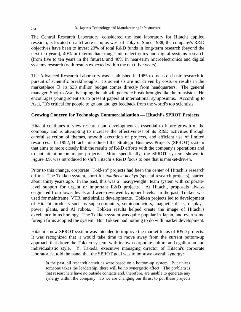
3. Japan’s Technology and Manufacturing Infrastructure56
The Central Research Laboratory, considered the lead laboratory for Hitachi appliedresearch, is located on a 51-acre campus west of Tokyo. Since 1988, the company's R&Dobjectives have been to invest 20% of total R&D funds in long-term research (beyond thenext ten years), 40% in intermediate-range microelectronics and digital systems research(from five to ten years in the future), and 40% in near-term microelectronics and digitalsystems research (with results expected within the next five years).
The Advanced Research Laboratory was established in 1985 to focus on basic research inpursuit of scientific breakthroughs. Its scientists are not driven by costs or results in themarketplace its $33 million budget comes directly from headquarters. The generalmanager, Shojiro Asai, is hoping the lab will generate breakthroughs like the transistor. Heencourages young scientists to present papers at international symposiums. According toAsai, "It's critical for people to go out and get feedback from the world's top scientists."
Growing Concern for Technology Commercialization — Hitachi’s SPROT Projects
Hitachi continues to view research and development as essential to future growth of thecompany and is attempting to increase the effectiveness of its R&D activities throughcareful selection of themes, smooth execution of projects, and efficient use of limitedresources. In 1992, Hitachi introduced the Strategic Business Projects (SPROT) systemthat aims to more closely link the results of R&D efforts with the company's operations andto put attention on major projects. More specifically, the SPROT system, shown inFigure 3.9, was introduced to shift Hitachi’s R&D focus to one that is market-driven.
Prior to this change, corporate "Tokken" projects had been the center of Hitachi's researchefforts. The Tokken system, short for tokubetsu kenkyu (special research projects), startedabout thirty years ago. In the past, this was a "heavyweight" team system with corporate-level support for urgent or important R&D projects. At Hitachi, proposals alwaysoriginated from lower levels and were reviewed by upper levels. In the past, Tokken wasused for mainframe, VTR, and similar developments. Tokken projects led to developmentof Hitachi products such as supercomputers, semiconductors, magnetic disks, displays,power plants, and AI robots. Tokken results helped create the image of Hitachi'sexcellence in technology. The Tokken system was quite popular in Japan, and even someforeign firms adopted the system. But Tokken had nothing to do with market development.
Hitachi’s new SPROT system was intended to improve the market focus of R&D projects.It was recognized that it would take time to move away from the current bottom-upapproach that drove the Tokken system, with its own corporate culture and egalitarian andindividualistic style. Y. Takeda, executive managing director of Hitachi's corporatelaboratories, told the panel that the SPROT goal was to improve overall synergy:
In the past, all research activities were based on a bottom-up system. But unlesssomeone takes the leadership, there will be no synergistic affect. The problem isthat researchers have no outside contacts and, therefore, are unable to generate anysynergy within the company. So we are changing our thrust to put these projects
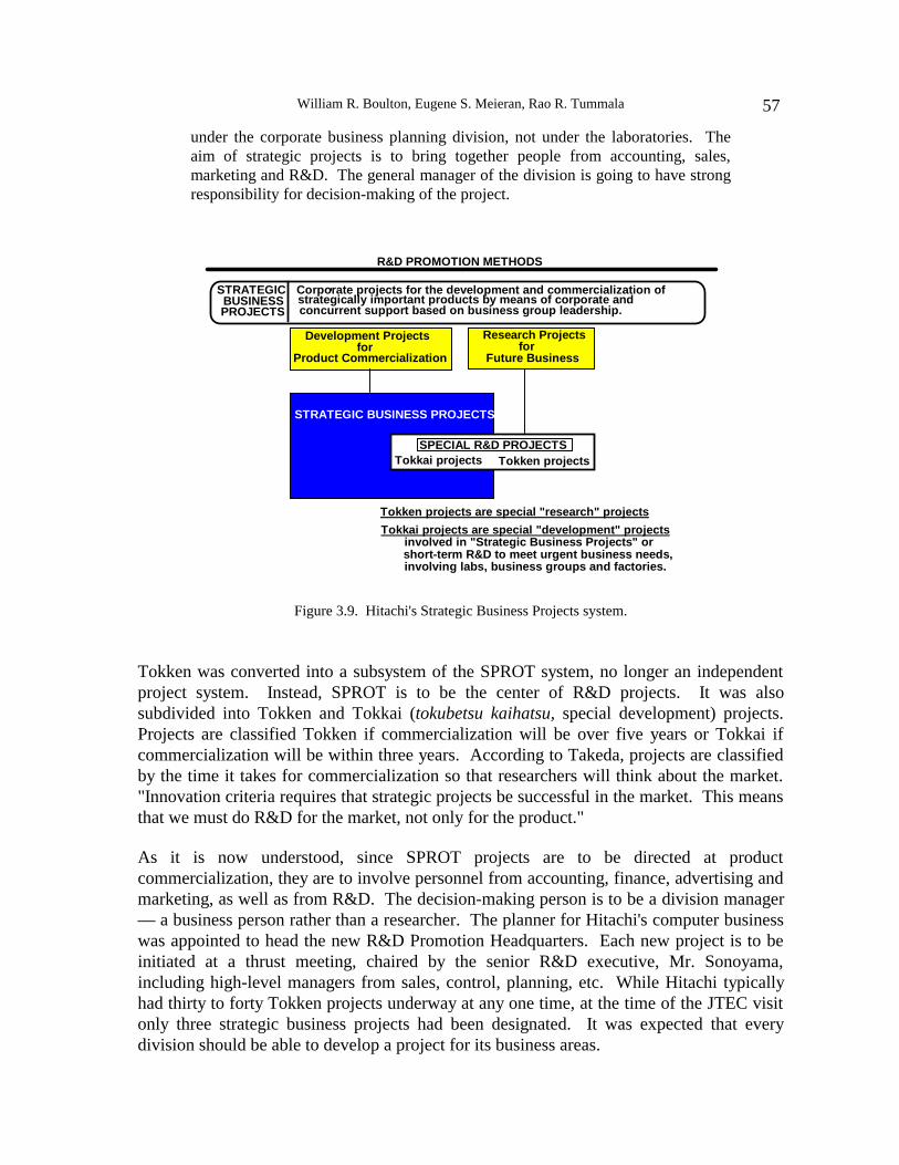
William R. Boulton, Eugene S. Meieran, Rao R. Tummala 57
under the corporate business planning division, not under the laboratories. Theaim of strategic projects is to bring together people from accounting, sales,marketing and R&D. The general manager of the division is going to have strongresponsibility for decision-making of the project.
STRATEGIC BUSINESS PROJECTS
SPECIAL R&D PROJECTSTokkai projects Tokken projects
Tokkai projects are special "development" projects
Tokken projects are special "research" projects
R&D PROMOTION METHODS
STRATEGICBUSINESSPROJECTS
Corporate projects for the development and commercialization ofstrategically important products by means of corporate andconcurrent support based on business group leadership.
involved in "Strategic Business Projects" orshort-term R&D to meet urgent business needs,involving labs, business groups and factories.
Development Projectsfor
Product Commercialization
Research Projectsfor
Future Business
Figure 3.9. Hitachi's Strategic Business Projects system.
Tokken was converted into a subsystem of the SPROT system, no longer an independentproject system. Instead, SPROT is to be the center of R&D projects. It was alsosubdivided into Tokken and Tokkai (tokubetsu kaihatsu, special development) projects.Projects are classified Tokken if commercialization will be over five years or Tokkai ifcommercialization will be within three years. According to Takeda, projects are classifiedby the time it takes for commercialization so that researchers will think about the market."Innovation criteria requires that strategic projects be successful in the market. This meansthat we must do R&D for the market, not only for the product."
As it is now understood, since SPROT projects are to be directed at productcommercialization, they are to involve personnel from accounting, finance, advertising andmarketing, as well as from R&D. The decision-making person is to be a division manager— a business person rather than a researcher. The planner for Hitachi's computer businesswas appointed to head the new R&D Promotion Headquarters. Each new project is to beinitiated at a thrust meeting, chaired by the senior R&D executive, Mr. Sonoyama,including high-level managers from sales, control, planning, etc. While Hitachi typicallyhad thirty to forty Tokken projects underway at any one time, at the time of the JTEC visitonly three strategic business projects had been designated. It was expected that everydivision should be able to develop a project for its business areas.

58 3. Japan’s Technology and Manufacturing Infrastructure
It is clear that Hitachi is constantly working to refine its market orientation and thereby theefficiency and long-term viability of its operations: It expects to be around “one thousandyears hence.” However, despite the company’s successful development of new technology,this has not been adequate to compete with technologically applied companies like Sony,Sharp, or Matsushita. To stay competitive, Hitachi, like many U.S. firms, is also having tolearn how to commercialize its technologies more rapidly.
CONCLUSION
While the United States may be a nation of explorers, entrepreneurs, innovators, andinventors who have developed products like the airplane, TV, personal computer, videotape machine, and cellular phone, the United States has had difficulty maintainingleadership in many of these industries. Being "first to market" has not guaranteed successin developing next-generation products. It has been Japanese companies with expertise inminiaturization technologies and manufacturing equipment that have garnered thecompetitive advantages in developing next-generation products.
The Japanese companies look for new growth markets where they can apply theirminiaturization and manufacturing skills to next-generation products. By identifying andsolving difficult technical problems, the Japanese have been able to outperform U.S. firmsin many industries. Motorola is one of the few U.S. firms that has been able to maintain itsmarket position by continuously miniaturizing its products and applying advancedmanufacturing technologies to cellular telephones.
In electronic packaging, Japan's vast supplier base is constantly working to solve thetechnical problems related to next-generation products. Thanks to leadership at thenational level and ongoing, industry-wide communication and cooperation, everyoneunderstands the technical requirements, and the microelectronics industry is focused onsolving the most difficult technical problems. Clear market orientation, nurturing of intra-industry and industry-public sector interdependence, good communication, and on-goingresearch and development of component and process technology as well as new technologyall seem to be critical components of Japan’s microelectronics industry infrastructure.
REFERENCES
Dodwell Marketing Consultants. 1993. Structure of the Japanese Electronics Industry. Tokyo.
U.S. Department of Commerce Technology Administration (DOC/TA). 1993 (May 3). Report ofthe U.S.-Japan Technology Transfer Joint Study Panel. PB93-182921.
U.S. Department of Commerce (DOC). 1993. U.S. Research Facilities of Foreign Companies.
Japan Science and Technology Agency (STA). 1992 (February). Survey Report on ResearchActivities in Private Enterprises.
Ministry of International Trade and Industry of Japan (MITI). 1991. “The 4th Basic Survey onJapanese Business Activities Abroad.” MITI News No. 3.
59
CHAPTER 4
JAPAN'S ELECTRONIC PACKAGING TECHNOLOGIES
Rao R. TummalaMichael Pecht
The JTEC panel found Japan to have significant leadership over the United States in thestrategic area of electronic packaging. Many technologies and products once consideredthe "heart and soul" of U.S. industry have been lost over the past several decades to Japanand other Asian countries. The loss of consumer electronics technologies and products isthe most notable of these losses, because electronics is the United States' largestemployment sector and is critical for growth businesses in consumer products, computers,automobiles, aerospace, and telecommunications. In the past there was a distinctionbetween consumer and industrial product technologies. While Japan concentrated on theconsumer market, the United States dominated the industrial sector. No such distinction isanticipated in the future; the consumer-oriented technologies Japan has dominated areexpected to characterize both domains. The future of U.S. competitiveness will thereforedepend on the ability of the United States to rebuild its technological capabilities in thearea of portable electronic packaging.
INTRODUCTION
A 1993 study by MCC and Sandia National Laboratory on U.S. industrial competitivenessin electronic packaging technology concluded the following:
• U.S. companies lead the world in several integrated circuit (IC) markets, butthis lead is weakened by an ill-equipped low-cost packaging infrastructure.
• Japanese IC packaging and assembly are significantly superior in terms ofminiaturization and cost-effectiveness.

4. Japan’s Electronic Packaging Technologies60
• Japanese market share in consumer electronics has created the "product pull"required to justify large investments in manufacturing processes that in turnhelp all other electronic segments, such as supercomputers andtelecommunications (MCC/Sandia 1993).
As shown in Figure 4.1, the United States leads in microprocessors, computer systems,software, and industrial electronics markets, while Japan is a clear leader in DRAMs,batteries, displays, and electronic packaging technologies that support its domination ofconsumer electronics markets.
INDUSTRIALMARKETS
(U.S. Leads)
CONSUMERMARKETS
(Japan Leads)
KEYCOMPONENTS
TECHNOLOGIESElectronic Packaging
BatteriesDisplaysDRAMS
(Japan Leads)
Microprocessors(U.S. Leads)
MATERIALSTECHNOLOGY:
CeramicsEpoxies
(Japan Leads)
PROCESSTECHNOLOGY
(Japan Leads)
SOFTWARE/SYSTEMS/
DESIGN(U.S. Leads)
PRODUCTIONEQUIPMENT
ANDCONTROLS
TECHNOLOGY(Japan Leads)
Communication
Information
Figure 4.1. Japan’s technological and market leadership.
As packaging technologies and related components become essential to next-generationproducts, an increasing proportion of components and equipment required for theproduction of commercial products must be imported by the United States from Japan orother Asian countries. The market for such imports is expected to exceed $100 billion bythe year 2000, a tenfold increase over today’s market.
JAPAN'S ELECTRONIC PACKAGING STRATEGIES
As Figure 4.2 shows, Japan’s competitive edge over the United States in electronicpackaging derives from the breadth of its packaging expertise. There are few areas inwhich Japan lags the United States. In fact, Japan is covering all its bases by investing inpackaging technologies that are required to protect existing markets and in newtechnologies to grow next-generation electronics markets. The Japanese electronics
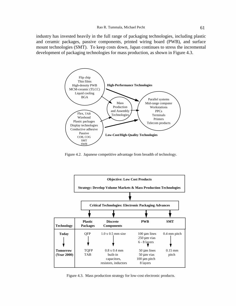
Rao R. Tummala, Michael Pecht 61
industry has invested heavily in the full range of packaging technologies, including plasticand ceramic packages, passive components, printed wiring board (PWB), and surfacemount technologies (SMT). To keep costs down, Japan continues to stress the incrementaldevelopment of packaging technologies for mass production, as shown in Figure 4.3.
Figure 4.2. Japanese competitive advantage from breadth of technology.
Figure 4.3. Mass production strategy for low-cost electronic products.
Parallel systemsMid-range computer
WorkstationsPPCs
TerminalsPrinters
Telecom products
MassProduction
and AssemblyTechnologiesFlex, TAB
WirebondPlastic packages
Display technologiesConductive adhesive
PassiveCOB, COG
SMTSWB
Flip chipThin films
High-density PWBMCM-ceramic (TLCC)
Liquid coolingBGA
High-Performance Technologies
Low-Cost/High-Quality Technologies
Critical Technologies: Electronic Packaging Advances
Objective: Low Cost Products
Strategy: Develop Volume Markets & Mass Production Technologies
QFP 1.0 x 0.5 mm size 100 µm lines 0.4 mm pitch 250 µm vias
6 - 8 layers
TQFP 0.8 x 0.4 mm 50 µm lines 0.15 mm TAB built-in 50 µm vias pitch capacitors, 100 µm pitch resistors, inductors 8 layers
Plastic Discrete PWB SMTPackages ComponentsTechnology
Today
Tomorrow(Year 2000)

4. Japan’s Electronic Packaging Technologies62
The JTEC panel's research suggests that Japanese firms will continue to push theminiaturization of electronic packaging technologies. Plastic packaging technologies willcontinue to evolve low-cost quad flat packs (QFP) into thinner and smaller-profilepackages such as thin quad flat packs (TQFP) and tape-automated bonding (TAB)packages. The high-volume applications of discrete components are expected to continueto shrink in size from the current 1.0 x 0.5 mm to 0.8 x 0.4 mm built-in multichip packagesof capacitors, resistors, and inductors. Printed wiring boards will also reduce line and viawidths from the current 100 µm and 250 µm, respectively, to 50 µm. The current six-to-eight-layer boards are expected to average eight layers. All these technologies are expectedto continue to be applied to surface mount applications. The current limit of 0.4 mm pitchin SMT applications is expected to reach 0.15 mm pitch by the turn of the century.
For nearly a decade, the camcorder has driven packaging technology developments forminiaturization, reduced weight, and digitization. As shown in Figure 4.4, this has drivenIC packaging to fine-pitch and thin packages while pushing the exploitation of multichipmodules. Since the early 1990s, cellular telephones have added pressure forminiaturization through increased functional integration. Today, personal computers areadding pressure for higher speed and multiple functions. The result is a push fordevelopment of new heat-dissipation solutions and for development of vertical packages.Japan’s continued economic success is expected to rely on its ability to maintain leadershipin a broad range of packaging technologies to achieve competitive cost reductions forfuture “personal electronic” units.
Figure 4.4. Electronic packaging trends (Matsushita Electric Co., Inc.).
Integration
Heat radiation
Multichip module
Thin package
HIGH DENSITY ASSEMBLY
TCP hot-bar reflowFine pitch QFP mass reflow
BGA mass reflowCOB low-temp. bonding
Mix mfg.: COB & mass reflowMultichip modulesRepair technologyNo clean soldering
Fine pitch
Vertical package
PERSONAL COMPUTERHigh speed
MultifunctionMiniaturization
CELLULAR TELEPHONEMiniaturization
Light weightHigh frequency
CAMCORDERMiniaturization
Light weightDigitization
Electronic Trend IC Packaging Board Assembly

Rao R. Tummala, Michael Pecht 63
The trend towards finer pin pitch creates a number of issues that must be addressed. Forexample, open leads and solder bridging must be prevented. The corresponding size ofsolder balls must also be reduced. Thin, small-outline packages (TSOP) require improvedresins and filler materials to reduce cracking during IR reflow. New designs for heatdissipation include the addition of heat-sinks under the die. Package miniaturizationrequires further developments in high-density board assembly.
PLASTIC PACKAGING TECHNOLOGIES
With the development of enhanced materials and production methods, plastic packaginghas become the low-cost, acceptable-reliability package of choice. Japan’s electronicsindustry is committed to incremental continuous improvements in all areas of chip makingand package assembly technologies. Professor Kenji Otsuka of Meisei University told theJTEC panel, "If we would lose packaging (plastic) technologies, we would get winterseason for a long time."
Thin, small-outline packages, with their compact profiles, have become a key product ofthe 1990s. By most estimates, they will also be used increasingly in surface mountpackages in the future, especially for memories, as demand for space-saving packagesgrows. Other thin package types include the thin quad flat pack (TQFP), thin sealed smalloutline (TSSOP), and thin-body plastic dual in-line (PDIP) packages. Integrated circuitpackages with width and/or length shrink include the fine-pitch quad flat pack (FPQFP),quartersize small outline package (QSSOP), shrink dual in-line processing (SDIP), shrinkquad flat pack (SQFP), shrink small outline package (SSOP) and very small outlinepackage (VSOP). With these or new shrunken packages, suppliers will continue to providemore functions in less board space, and boards will become smaller. This trend to skinnierhousings will challenge die thinning, wafer transportation, chip pad mounting, leadframedesign, lead bonding, board interconnection, molding, and soldering technologies.
Continued development of plastic packaging technologies, as discussed above, is essentialto support Japan's focus on low-cost consumer electronics products. As shown inFigure 4.5, plastic QFP remains the low-cost single chip electronic packaging technology.TAB is higher-cost but is utilized in cases where finer pitch is required to achieveminiaturization objectives. Ceramic pin grid array (PGA) is the highest-cost technologyand is generally limited to uses where reliability and performance are critical.
Present packaging issues depend on different uses for plastic quad flat packs (P-QFP) inJapanese and U.S. manufacturing. The U.S. Joint Electron Devices Engineering Council(JEDEC) is addressing the problems of bond pad pitch requirements finer than 0.65 mm(26 mils). A few Japanese manufacturers have tooled for 0.5 mm (20 mils) pitch partsand have plans for smaller pitch in various stages of development. The ElectronicIndustry Association of Japan P-QFP version has received wider acceptance by ASIC(application-specific integrated circuit) users and manufacturers, since greater volumeshave been generated at lower costs than for the U.S. JEDEC version.

4. Japan’s Electronic Packaging Technologies64
P-PGA (3 layers)
P-PGA (8 layers)
P-QFP (2-3 layers)
TAB (1 layer)
P-QFP (1 layer)
C-PGA (12 layers)
100000
10000
1000
100
Pac
kage
mat
eria
l pric
e (y
en)
1000 200 300 400 500 600 700
Pin count
TAB (2 layers)
C-PGA(3 layers)
Figure 4.5. Single chip packaging costs (Otsuka).
Plastic Molding Materials and Processes
As shown in Table 4.1, Nitto Denko is working to improve and develop molding materialsto meet the needs of future packages. Manufacturing technology and the cost of advancedmaterials required for high-quality and reliable plastic packaging determine bothacquisition and lifetime cost, and drive technology for the widespread use of plastic epoxymolded (PEM) packages in all markets. Performance criteria naturally adapt to the costconstraints of the market. The high-performance molding processes of the most commonpackages produces about 800 packaged devices per hour.
Future packages using thinner leadframes, fine-pitch wire bonding, and flip chip or TABstructures will need low-viscosity molding compounds at low molding temperatures toreduce shear-rate-induced yield losses. Higher production rates are required to competewith PGAs and premolded packages. Smaller molds with fewer cavities and a total cycletime (including in-mold cure) of one to two minutes will be needed. A high level ofautomation will result in lower-cost, uniform-quality packages with less damage to fragilehigh-I/O-count assemblies. Clean manufacturing environments will also reducecontamination-related failures.

Rao R. Tummala, Michael Pecht 65
Table 4.1Molding Compound Development in Japan
Source: Nitto Denko
Automation will play an increasingly important role in PEM manufacturing in Japan. Oneapproach is partial automation of various labor-intensive aspects of the process, such aspreform heating and handling. A robotic arm may place the heated preform into thetransfer pot and start the process sequence of transferring, curing, and ejecting the moldedleadframes. In this automation approach, a single operator can handle four or five transferpresses. In the total automation approach, the process runs without any operator assistance,although typically 10 to 20% of an operator’s time is spent moving different cassettes andchecking equipment malfunctions. The use of a smaller molding tool with fewer cavitiesin conjunction with faster-curing molding compounds will further increase productivity.Such a packaging system is usually totally enclosed to maximize process cleanliness andpersonnel safety. The cassettes of molded leadframes feed an automated trim-and-formpress and then move on to a code-marking station.
The partial or total automation of single-pot systems has been superseded by multiplungertechnology in multiproduct production environments. In automated multiplunger systems,6 to 12 pots feed 6 to 24 cavities, with 1 to 4 cavities per transfer pot. Because of the veryshort flow length, they are very effective in minimizing voids and promoting high moldingcompound density. State-of-the-art encapsulants, i.e., very fast-curing molding compoundswith a total cycle time of less than two minutes in the molds, will be used in thesemanufacturing systems. Figure 4.6 shows the trend in encapsulant molding compounds.
Process Controls and Quality Assurance
Stringent contamination control of package assembly components during fabrication ofPEMs is necessary for quality assurance and long-term reliability. Over and above thepractice of using semiconductor fabrication type class 100,000 or better clean-room
Discrete MP-2000 Moldability
1970s Small DIPMiddle DIPLarge DIP, SOP
MP-3000HC-10-2MP 150SG
Moisture resistance, moldability “ “ “Low stress
1980s PLCCQFPSSOP, TSOPSQFP, TQFP
MP-180MP-190MP-7000MP-7000
Low stressLow stress, processabilitySoldering resistance “ “
1990s SOP, DIPPLCC, QFPLarge packageUltrathin packageSpecific package
MP-80MP-8000Target 1Target 2Target 3
Anti-delamination, processabilityFloor life for soldering, low stress, high adhesionSoldering resistance, low stress, moldabilityMoldability, soldering resistanceAdaptability to components

4. Japan’s Electronic Packaging Technologies66
Reliability
(temperature, humidity bias)
Composition
and formulation
Moldability
(viscosity control)
Low stress, humidity resistance
(megabit memories)
Resin flexibilation, hardener,
coupling agent, etc.
Thermal conductivity for
moldability and reliability
(high heat dissipation devices)
Filler type and composition
Non post-cure type with high
glass transition temperature
(integrated circuit, large scale
integration)
Catalyst
Non cleaning type for
demoldability and reliability
(integrated circuit, large scale
integration)
Basic resin release agent
Low viscosity compound,
curing agent, additives
Molding compound for
multiplier use with high
fluidity and optimized cure
(integrated circuit, large
scale integration)
Epoxy Molding Compound
Research and Development
Figure 4.6. Current development trends of epoxy molded compounds.
Rao R. Tummala, Michael Pecht 67
operation, high-technology integrated-circuit wafer cleaning processes will increasinglyspread into packaging process technology. Plasma cleaning of the pad and leadframeassembly for improved bonding with plastics may become widespread. As a function ofoxygen/carbon tetrafluoride/argon plasma treatment, lap-shear strength of epoxy adhesivesshould increase. Ultrahigh purity chemicals are sure to find their way into PEM fabricationlines as initial cleaning agents for particulate contamination control.
The increasing use of analytical techniques and microsensors to fine-tune materials andcontrol process-induced defects falls into the category of enhanced process control andquality assurance. X-ray radiography and C-mode scanning acoustic microscopy-tomography are finding increased use as nondestructive techniques for evaluating a numberof processes: plastic delamination; die metal, die attach and bonding wire deformation; diemetal and wirebond voiding; leadframe, die passivation, die attach, wire, wirebond andcase brittle fracture; and dendritic growth under bias. Mercury porosimetry has also beenused successfully to find the number and size of epoxy and epoxy-metal pores in epoxy-encapsulated packages. Epoxy pores are less than 0.2 µm in diameter, epoxy-leadframesvoids are about 1 µm in diameter, and surface pores range from 5-500 µm in diameter.Piezoresistive strain gauges integrated into test chips will continue to be used to directlymeasure the mechanical stress induced inside a PEM by encapsulation, die bonding, andother factors, either during fabrication or under environmental stress testing. Solid-statemoisture microsensors will also be used to measure the moisture content at any specificlocation inside a PEM.
Fine-Pitch Interconnections
Challenged by higher integration levels (particularly in ASICs) with tighter bond padpitches at the die level, leading edge pitches will be at 0.060 to 0.075 mm (2.5 to 3 mils) bythe late 1990s. Beyond 0.1 mm (4 mils) pitch, bonding with gold wire may be done bywedge bonding. The combination of tight pad pitches and shrink packages demands notonly low wire looping (0.09 to 0.18 mm), but also different loop shapes. This requiresmodifying the dopants in the wire to offer the right set of mechanical properties. With tightpitches, the physical limits of leadframe technology will also force the placement of leadcontacts at ever-increasing distances from the package center to control wire sweep. Lowlooping also promotes wire-to-die edge shortening when the die has inbound bonding padsto avoid encapsulation stress concentration zones. Edge shortening can be prevented byuse of wirebonder software that allows an extra bend in the wire at the predetermined site.
The demands of tightly spaced inner-lead bonding (0.05 to 0.075 mm) and outer-leadbonding (0.15 to 0.35 mm), high pin counts, high-end performance-driven applications,and high-volume production, could also move bumped tape automated bonding (TAB) tothe forefront of the packaging industry — a potential for which Japan already has thecapability and infrastructure. Limiting factors for TAB application have been the expenseof tape, the lead time needed to obtain it, and the capital needed for the bonding equipment.Bump fabrication has also been an obstacle. Better tape metallurgy, currently available,
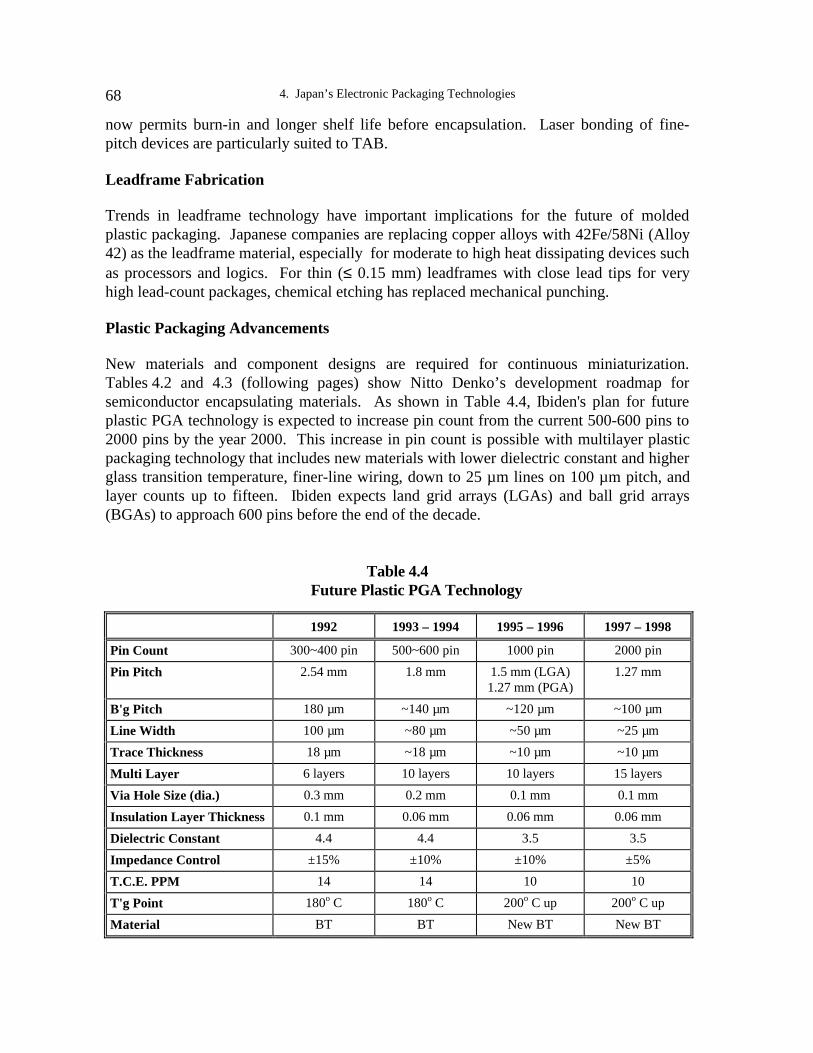
4. Japan’s Electronic Packaging Technologies68
now permits burn-in and longer shelf life before encapsulation. Laser bonding of fine-pitch devices are particularly suited to TAB.
Leadframe Fabrication
Trends in leadframe technology have important implications for the future of moldedplastic packaging. Japanese companies are replacing copper alloys with 42Fe/58Ni (Alloy42) as the leadframe material, especially for moderate to high heat dissipating devices suchas processors and logics. For thin (≤ 0.15 mm) leadframes with close lead tips for veryhigh lead-count packages, chemical etching has replaced mechanical punching.
Plastic Packaging Advancements
New materials and component designs are required for continuous miniaturization.Tables 4.2 and 4.3 (following pages) show Nitto Denko’s development roadmap forsemiconductor encapsulating materials. As shown in Table 4.4, Ibiden's plan for futureplastic PGA technology is expected to increase pin count from the current 500-600 pins to2000 pins by the year 2000. This increase in pin count is possible with multilayer plasticpackaging technology that includes new materials with lower dielectric constant and higherglass transition temperature, finer-line wiring, down to 25 µm lines on 100 µm pitch, andlayer counts up to fifteen. Ibiden expects land grid arrays (LGAs) and ball grid arrays(BGAs) to approach 600 pins before the end of the decade.
Table 4.4Future Plastic PGA Technology
1992 1993 – 1994 1995 – 1996 1997 – 1998
Pin Count 300~400 pin 500~600 pin 1000 pin 2000 pin
Pin Pitch 2.54 mm 1.8 mm 1.5 mm (LGA)1.27 mm (PGA)
1.27 mm
B'g Pitch 180 µm ~140 µm ~120 µm ~100 µm
Line Width 100 µm ~80 µm ~50 µm ~25 µm
Trace Thickness 18 µm ~18 µm ~10 µm ~10 µm
Multi Layer 6 layers 10 layers 10 layers 15 layers
Via Hole Size (dia.) 0.3 mm 0.2 mm 0.1 mm 0.1 mm
Insulation Layer Thickness 0.1 mm 0.06 mm 0.06 mm 0.06 mm
Dielectric Constant 4.4 4.4 3.5 3.5
Impedance Control ±15% ±10% ±10% ±5%
T.C.E. PPM 14 14 10 10
T'g Point 180o C 180o C 200o C up 200o C up
Material BT BT New BT New BT

Table 4.2Development Roadmap of Semiconductor Encapsulating Material
Courtesy of Nitto Denko
Category 1992 1993 1994 1995low temp mold
small package solder dip & PCT (for PPF) goodDesign low stress fast cure longer floor life processability
Technology anti-delamination no post cureStandard MC anti-solder anti-solder & anti-solder (super thin)
(thin package) moldabilityanti-solder anti-solder anti-solder anti-solder
(large package) (thick package) (large package) (large & thin)power device good low stress & antilarge/special processability abrasiveness high thermal conductive & anti-solder
Special MC package MC for heatdissipation package
MC for MCM
TAB MC for small TAB MC for large TABnew inflammable recyclable
System new polymer polyimide material (harmless) recovery or cullTechnology multifunction
new system liquid encapsulating encapsulatingkneading high filler content
Manufacturing pelletizing dust-free pelletTechnology new manufacturing process for new
system encapsulatedsystem
analysis of analysis ofmoldability void/delamination pap-tilt, etc.
Evolution analysis ofTechnology flow process simulation by FEM application of simulation result
reliability adhesion studyapplication of
the study

Table 4.3Development Roadmap of Semiconductor Encapsulating Material (Part 2)
Courtesy of Nitto Denko
1993 1994 1995 1996 Requirements Nitto’s products
ProcessInnovation
No PMCPPF
Laser marking Bottom mark lessDie bond snap cure
Single device burn-in Wafer burn-inClean mold system
1. PMC free2. Low temperature3. Package traceability4. High-performance die attach5. Wafer burn-in6. Dust free
MCMCMicro print systemElep mount system
ASMATCT, new encapsulant
PackageInnovation
Ball grid array 1. No warpage, no delamination
MC, elep mount system
Fine PitchFlip chip, TAB
Dam bar less Increasing bonding pad
2. Filling space3. Dam bar less4. High humidity resistance
New encapsulantNew materialMC
ThinnerPackageMultilayer
1 mmt 0.5 mmt TCPMCM Multilayer MCM
1. Good moldability Anti-popcorn Warpage free2. Buffer, low stress3. Casting
MC, elep mount systemLamination material
MC, new materialLiquid encapsulant
High PowerHighFrequency
Package with large heat spreaderHigh thermal radiation
High temp. storage Dielectric loss Noise problem ESD problem
1. New combination2. High lambda3. Heat resistance4. Low dielectric loss5. Shielding6. Protect from static electricity
MC. elep mountMCPolyimide encapsulantNew encapsulantNew system(multilayer encapsulant)
Local StressSoft Error
Gel coat Cavity mold Gel coat less
Data retention error
1. Buffer2. New system3. Low stress
MC, die coatingCavity packageMCBuffers for local stress
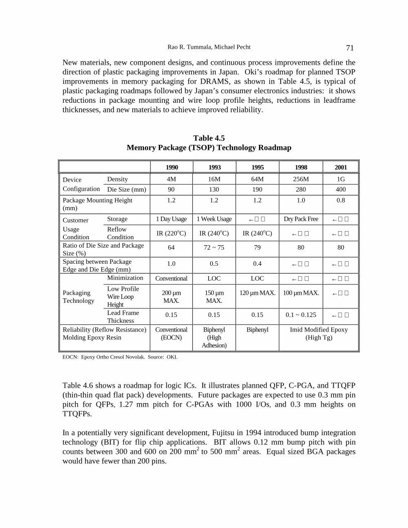
Rao R. Tummala, Michael Pecht 71
New materials, new component designs, and continuous process improvements define thedirection of plastic packaging improvements in Japan. Oki’s roadmap for planned TSOPimprovements in memory packaging for DRAMS, as shown in Table 4.5, is typical ofplastic packaging roadmaps followed by Japan’s consumer electronics industries: it showsreductions in package mounting and wire loop profile heights, reductions in leadframethicknesses, and new materials to achieve improved reliability.
Table 4.5Memory Package (TSOP) Technology Roadmap
EOCN: Epoxy Ortho Cresol Novolak. Source: OKI.
Table 4.6 shows a roadmap for logic ICs. It illustrates planned QFP, C-PGA, and TTQFP(thin-thin quad flat pack) developments. Future packages are expected to use 0.3 mm pinpitch for QFPs, 1.27 mm pitch for C-PGAs with 1000 I/Os, and 0.3 mm heights onTTQFPs.
In a potentially very significant development, Fujitsu in 1994 introduced bump integrationtechnology (BIT) for flip chip applications. BIT allows 0.12 mm bump pitch with pincounts between 300 and 600 on 200 mm2 to 500 mm2 areas. Equal sized BGA packageswould have fewer than 200 pins.
1990 1993 1995 1998 2001
Device Density 4M 16M 64M 256M 1G
Configuration Die Size (mm) 90 130 190 280 400
Package Mounting Height(mm)
1.2 1.2 1.2 1.0 0.8
Customer Storage 1 Day Usage 1 Week Usage ← Dry Pack Free ←UsageCondition
ReflowCondition
IR (220oC) IR (240oC) IR (240oC) ← ←
Ratio of Die Size and PackageSize (%)
64 72 ~ 75 79 80 80
Spacing between PackageEdge and Die Edge (mm)
1.0 0.5 0.4 ← ←
Minimization Conventional LOC LOC ← ←
PackagingTechnology
Low ProfileWire LoopHeight
200 µmMAX.
150 µmMAX.
120 µm MAX. 100 µm MAX. ←
Lead FrameThickness
0.15 0.15 0.15 0.1 ~ 0.125 ←
Reliability (Reflow Resistance)Molding Epoxy Resin
Conventional(EOCN)
Biphenyl(High
Adhesion)
Biphenyl Imid Modified Epoxy(High Tg)
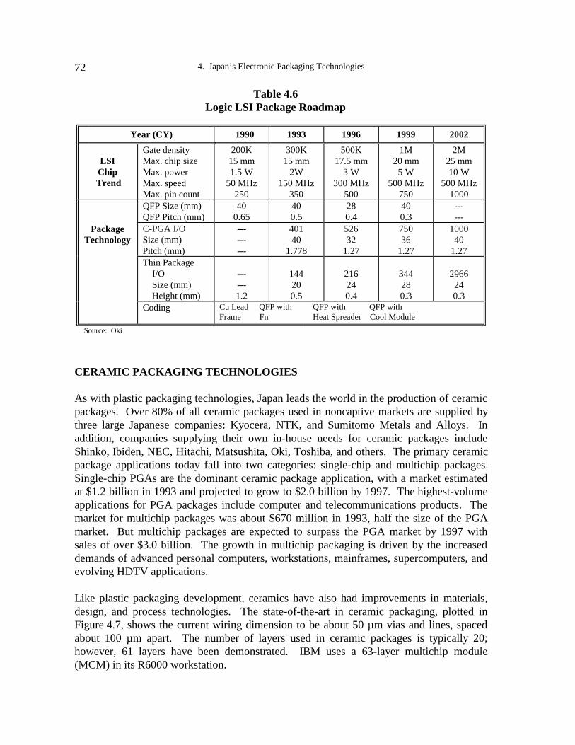
4. Japan’s Electronic Packaging Technologies72
Table 4.6Logic LSI Package Roadmap
Source: Oki
CERAMIC PACKAGING TECHNOLOGIES
As with plastic packaging technologies, Japan leads the world in the production of ceramicpackages. Over 80% of all ceramic packages used in noncaptive markets are supplied bythree large Japanese companies: Kyocera, NTK, and Sumitomo Metals and Alloys. Inaddition, companies supplying their own in-house needs for ceramic packages includeShinko, Ibiden, NEC, Hitachi, Matsushita, Oki, Toshiba, and others. The primary ceramicpackage applications today fall into two categories: single-chip and multichip packages.Single-chip PGAs are the dominant ceramic package application, with a market estimatedat $1.2 billion in 1993 and projected to grow to $2.0 billion by 1997. The highest-volumeapplications for PGA packages include computer and telecommunications products. Themarket for multichip packages was about $670 million in 1993, half the size of the PGAmarket. But multichip packages are expected to surpass the PGA market by 1997 withsales of over $3.0 billion. The growth in multichip packaging is driven by the increaseddemands of advanced personal computers, workstations, mainframes, supercomputers, andevolving HDTV applications.
Like plastic packaging development, ceramics have also had improvements in materials,design, and process technologies. The state-of-the-art in ceramic packaging, plotted inFigure 4.7, shows the current wiring dimension to be about 50 µm vias and lines, spacedabout 100 µm apart. The number of layers used in ceramic packages is typically 20;however, 61 layers have been demonstrated. IBM uses a 63-layer multichip module(MCM) in its R6000 workstation.
Year (CY) 1990 1993 1996 1999 2002
LSIChip
Trend
Gate densityMax. chip sizeMax. powerMax. speedMax. pin count
200K15 mm1.5 W
50 MHz250
300K15 mm
2W150 MHz
350
500K17.5 mm
3 W300 MHz
500
1M20 mm5 W
500 MHz750
2M25 mm10 W
500 MHz1000
QFP Size (mm)QFP Pitch (mm)
400.65
400.5
280.4
400.3
------
PackageTechnology
C-PGA I/OSize (mm)Pitch (mm)
---------
40140
1.778
52632
1.27
75036
1.27
100040
1.27Thin Package I/O Size (mm) Height (mm)
------1.2
144200.5
216240.4
344280.3
2966240.3
Coding Cu Lead QFP withFrame Fn
QFP with QFP with Heat Spreader Cool Module
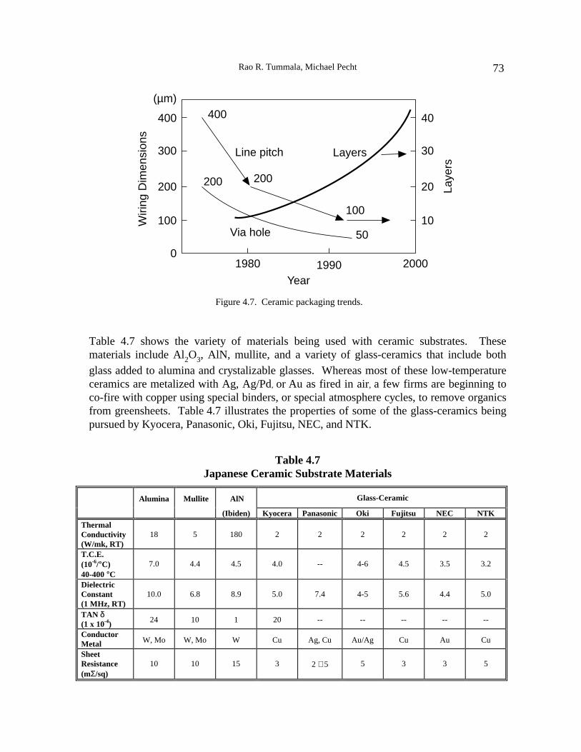
Rao R. Tummala, Michael Pecht 73
Line pitch
Via hole
400
300
200
100
01980 1990
(µm)
Year
400
200
100
50
200
2000
40
30
20
10
LayersW
iring
Dim
ensi
ons
Laye
rs
Figure 4.7. Ceramic packaging trends.
Table 4.7 shows the variety of materials being used with ceramic substrates. Thesematerials include Al2O3, AlN, mullite, and a variety of glass-ceramics that include bothglass added to alumina and crystalizable glasses. Whereas most of these low-temperatureceramics are metalized with Ag, Ag/Pd, or Au as fired in air, a few firms are beginning toco-fire with copper using special binders, or special atmosphere cycles, to remove organicsfrom greensheets. Table 4.7 illustrates the properties of some of the glass-ceramics beingpursued by Kyocera, Panasonic, Oki, Fujitsu, NEC, and NTK.
Table 4.7Japanese Ceramic Substrate Materials
Alumina Mullite AlN Glass-Ceramic
(Ibiden) Kyocera Panasonic Oki Fujitsu NEC NTKThermalConductivity(W/mk, RT)
18 5 180 2 2 2 2 2 2
T.C.E.(10-6/°C)40-400 °C
7.0 4.4 4.5 4.0 -- 4-6 4.5 3.5 3.2
DielectricConstant(1 MHz, RT)
10.0 6.8 8.9 5.0 7.4 4-5 5.6 4.4 5.0
TAN δ(1 x 10⁻⁴) 24 10 1 20 -- -- -- -- --
ConductorMetal W, Mo W, Mo W Cu Ag, Cu Au/Ag Cu Au Cu
SheetResistance(mΣ/sq)
10 10 15 3 2 ∼ 5 5 3 3 5
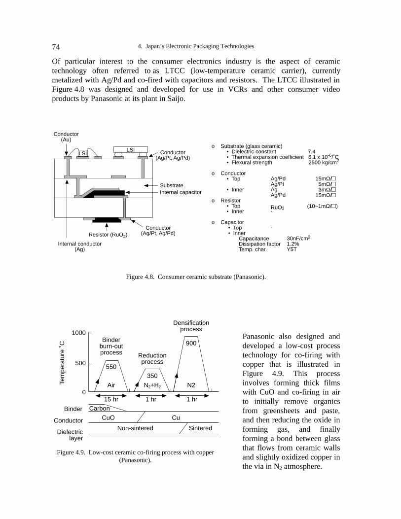
4. Japan’s Electronic Packaging Technologies74
Of particular interest to the consumer electronics industry is the aspect of ceramictechnology often referred to as LTCC (low-temperature ceramic carrier), currentlymetalized with Ag/Pd and co-fired with capacitors and resistors. The LTCC illustrated inFigure 4.8 was designed and developed for use in VCRs and other consumer videoproducts by Panasonic at its plant in Saijo.
LSILSI
Conductor(Au)
Conductor(Ag/Pt, Ag/Pd)
Internal capacitorSubstrate
Internal conductor (Ag)
Resistor (RuO2)Conductor
(Ag/Pt, Ag/Pd)
o Substrate (glass ceramic) • Dielectric constant 7.4 • Thermal expansion coefficient 6.1 x 10⁻⁶/˚C • Flexural strength 2500 kg/cm2
o Conductor • Top
• Inner
o Resistor • Top • Inner
o Capacitor • Top • Inner Capacitance Dissipation factor Temp. char.
Ag/PdAg/PtAgAg/Pd
RuO2-
-
15mΩ/ . 5mΩ/ .3mΩ/ .
15mΩ/ .
(10~1mΩ/ )
30nF/cm2
1.2%Y5T
Figure 4.8. Consumer ceramic substrate (Panasonic).
Panasonic also designed anddeveloped a low-cost processtechnology for co-firing withcopper that is illustrated inFigure 4.9. This processinvolves forming thick filmswith CuO and co-firing in airto initially remove organicsfrom greensheets and paste,and then reducing the oxide informing gas, and finallyforming a bond between glassthat flows from ceramic wallsand slightly oxidized copper inthe via in N2 atmosphere.
Binder burn-out process
550
Air
Reduction process
350
N2+H2
Densification process
900
N2
15 hr 1 hr 1 hrCarbon
Non-sintered Sintered
CuO Cu
1000
500
0
Tem
pera
ture
˚C
Binder
Conductor
Dielectriclayer
Figure 4.9. Low-cost ceramic co-firing process with copper(Panasonic).
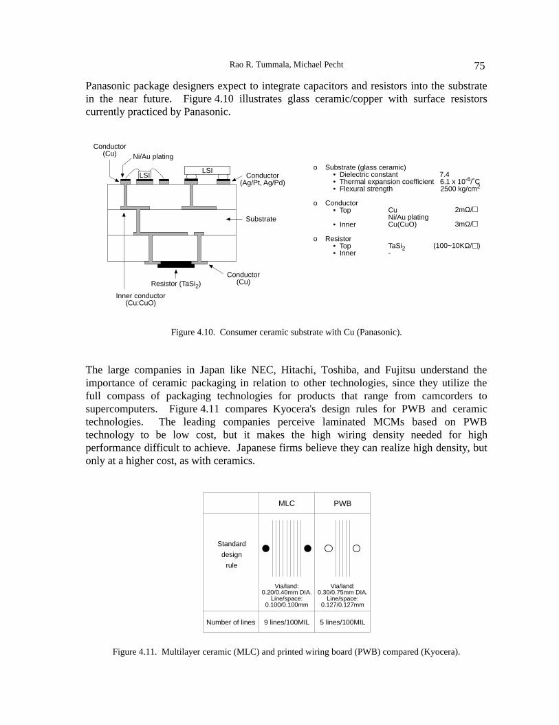
Rao R. Tummala, Michael Pecht 75
Panasonic package designers expect to integrate capacitors and resistors into the substratein the near future. Figure 4.10 illustrates glass ceramic/copper with surface resistorscurrently practiced by Panasonic.
LSILSI
Conductor(Cu)
Conductor(Ag/Pt, Ag/Pd)
Substrate
Inner conductor (Cu:CuO)
Resistor (TaSi2)Conductor
(Cu)
o Substrate (glass ceramic) • Dielectric constant 7.4 • Thermal expansion coefficient 6.1 x 10⁻⁶/˚C • Flexural strength 2500 kg/cm2
o Conductor • Top
• Inner
o Resistor • Top • Inner
CuNi/Au platingCu(CuO)
TaSi2-
2mΩ/ .
3mΩ/ .
(100~10KΩ/ )
Ni/Au plating
Figure 4.10. Consumer ceramic substrate with Cu (Panasonic).
The large companies in Japan like NEC, Hitachi, Toshiba, and Fujitsu understand theimportance of ceramic packaging in relation to other technologies, since they utilize thefull compass of packaging technologies for products that range from camcorders tosupercomputers. Figure 4.11 compares Kyocera's design rules for PWB and ceramictechnologies. The leading companies perceive laminated MCMs based on PWBtechnology to be low cost, but it makes the high wiring density needed for highperformance difficult to achieve. Japanese firms believe they can realize high density, butonly at a higher cost, as with ceramics.
PWB
Via/land: 0.20/0.40mm DIA.
Line/space: 0.100/0.100mm
Via/land: 0.30/0.75mm DIA.
Line/space: 0.127/0.127mm
9 lines/100MIL 5 lines/100MIL
Standard
design
rule
MLC
Number of lines
Figure 4.11. Multilayer ceramic (MLC) and printed wiring board (PWB) compared (Kyocera).

4. Japan’s Electronic Packaging Technologies76
Thin-film technology has been demonstrated and used by NEC in its mainframe andsupercomputers, but only at very high cost. NEC believes ceramic MCM technology hasthe best potential; where it lags, NEC plans to supplement with surface thin-film layer orlayers to achieve the required redistribution and wiring. NEC understands the costimplications of the technologies but has only recently been able to develop and deliver theceramic greensheets. A material that NEC recently developed, G100, has a dielectricconstant of 4.4 and is co-firable with gold, having a thermal expansion coefficient of4.5 x 10
-6/oC. The material used in accomplishing this 4.4 dielectric constant consists of
15% quartz glass plus 20% cordierite plus 65% borosilicate glass. Fired in air at 900°C,the material has a mechanical strength of 1600 kg/cm2. The ceramic packaging technologyroadmap followed by NEC during the last fifteen years is illustrated in Table 4.8.
Table 4.8NEC’s Ceramic Roadmap
NEC is exploring ways to achieve an even lower effective dielectric constant. One approachis to develop hollow space between ground and signal planes (Fig. 4.12). Plotting dielectricconstant and signal propagation delay for various NEC materials, including the newmaterial with and without the above hollow structure (Fig. 4.13), shows that 4.4 materialbehaves normally with signal propagation delay of 7.6 nsec/m, but the hollow structurebehaves as if it has dielectric planes. The transmission properties are greatly influenced bythe configuration of ground plane and wiring plane open area and signal line channel.
1980 1985-1990 (G10) 1990 1995 (G100)Aluminawith W
Glass + Ceramicwith Ag/Pd
Alumina + GlassGlass + Ceramic
Ag Rich/Pd
Cordierite + GlassGlass + Ceramic
GoldEr = 9
ρ = 15 µ ⋅ Ω ⋅ cmEr = 7.8
ρ = 10 µ ⋅ Ω ⋅ cmEr = 4.4
ρ = 3.5 µ ⋅ Ω ⋅ cm ρ = 3.0 µ ⋅ Ω ⋅ cm
spacea
b
GND2SIG
GND1
Pad
Model 1
Model 2
c
a
b
space
space
GND4SIGX
SIGYGND3
Figure 4.12. Hollow structure in ceramicfor improved dielectric constant.
AluminaGlass ceramic:
7.8
4.4
3.4 Hollow structure
Hollow structure
1 3 5 7 9 11
Dielectric Constant: ε
Sig
nal p
ropa
gatio
n de
lay
TP
D (
nsec
/m)
11
9
7
5
3
Figure 4.13. Propagation delay versusdielectric constant (NEC).

Rao R. Tummala, Michael Pecht 77
As illustrated in Figure 4.14, the rectangularopen area seems to give constant overlap areabetween ground pattern and signal line, thusminimizing the capacitance variation that istypical of conventional square mesh patterns.NEC has applied this new material for amedium-cost, 156 Mb/s optical inter-connectionmodule. In this application this technology hasreduced (1) the number of modules to one fromtwo from previous SMT/PWB technology, (2)the volume size by one-seventh, and (3) thepower consumption by one-third. The total sizeof the final unit is 10 cc. NEC expects to use thisnew ceramic package in its personal computersas an interface to the CRT.
Use of aluminum nitride is much more emphasized in Japan than in the United States.Ibiden, Kyocera, NTK, NEC, Toshiba, and Sumitomo Electric are some of the firms thathave invested very heavily in developing and producing AlN pin grid arrays, as well ashigh-thermal-conductivity heat sinks. Ibiden, for example, makes a large substrate by hotpressing to achieve a thermal conductivity of 180 W/mk. NEC claims to have achieved ashigh as 200 W/mk and has transferred the technology to its subsidiary. The Japanesemarket for AlN is currently estimated at $100 million per year, much less than previouslyprojected. The primary reason for this slow growth has been attributed to the twenty tothirty times higher raw material cost over standard alumina and the one-half to two timeshigher substrate cost. NEC expects to use AlN for high-performance applications requiringhigher thermal conductivity, where the additional cost can be justified.
A new ceramic substrate approach being pursued by Ibiden involves bonding epoxy-glassFR-4 layers to porous ceramic. Such a structure, illustrated in Figure 4.15, improves TCE,dielectric constant, and mechanical strength, and permits direct flip chip bonding.
Porous-ceramic & resin composite layer(porous-cordierite + epoxy resin)
Conductor layer (copper foil; 18µm)Reinforce layer(glass cloth + epoxy resin; 0.1mm)
Figure 4.15. Ceracom substrate with low TCE and low dielectric constant (Ibiden).
SIGX
SIGY
ec
d
Figure 4.14. Package designimprovement.

4. Japan’s Electronic Packaging Technologies78
PASSIVE COMPONENT TECHNOLOGIES
Passive components are important contributors to the miniaturization of most electronicproducts. Passives include capacitors, resistors, piezoelectrics, and coils. Heavy relianceon analog circuitry requires a large number of passive components to be used in consumerproducts like VCRs, camcorders, and cellular phones. In Hitachi’s video camera, forexample, there are currently 475 passive components required. Current development planswill reduce that number to 290, as illustrated in Figure 4.16. Continued miniaturization isexpected to reduce power consumption as the number of ICs and passive components aredecreased for smaller and lighter products. The miniaturization trend for coils andcapacitors is illustrated in Table 4.9.
As with plastic and ceramic packaging technologies, Japanese firms also lead in passivecomponent technologies. Three Japanese companies, Murata, TDK, and Kyocera (AVX inthe United States), account for most of the world market in this industry.
Japanese investments in passive component developments are aimed at continuedreduction of cost and size rather than increased integration. Integration was used toachieve miniaturization requirements, but was often considered to be a higher-cost or next-generation alternative. The primary R&D activities pursued by Murata, as an example,include the following:
Table 4.9 Component Miniaturization
Year Coil Size CapacitorSize
1986 26 x 17 x 10 mmalumina thick filmco-axial resonator
3.2 x 1.6mm
1990 16 x 12 x 4.0 mmglass-epoxy subst.co-axial resonator
2.1 x 1.25mm
1992 10 x 10 x 4.0 mmmultilayer ceramictriplate resonator
- - -
1993 10 x 7 x 2.5 mmmultilayer ceramictriplate resonator
1.0 x 0.5mm
1997 7 x 7 x 2.5 mmmultilayer ceramictriplate resonator
ModuleIntegration
Relative cost
Relative size
ICS
Passives
Power6
290
1
Re
lativ
e c
ha
ract
erist
ics
1990 1995 2000
Year
11
475
2.3
watts
Figure 4.16. Components trend in camcorders(Hitachi).
Rao R. Tummala, Michael Pecht 79
• microwave modules for digital cordless phones:oscillator, mixer, synthesizer developments
• power supplies (SW frequency 2 MHz):CAD, substrate, transformer, capacitor, package developments
• functional sensor module:gyro sensor, IR sensor, signal processing developments through technology integration
• capacitor (miniaturization and higher capacitance):thin-film multilayer, ceramic, reliability, electrode material developments
• filter (for communications):piezoelectric ceramic products, high ceramics, thin-film process
The JTEC panel was most impressed with the passive component technology andmanufacturing capabilities of the Japanese firms visited. Companies like Murata andTDK, for example, have highly automated factories and produce their own in-houseequipment to manufacture millions of parts, some the size of poppy seeds, using multilayermetalization and dielectrics.
ADVANCED MULTICHIP PACKAGING DEVELOPMENTS
Multichip packaging is being developed to meet the demands for higher performance andfurther miniaturization. These design developments apply array technologies, SMT, and avariety of plastic, ceramic and thin-film materials. Advanced technologies like BGAs andMCMs have historically been limited to applications in high-performance products likesupercomputers. Today, the Japanese are moving these technologies into lower-costproducts through the use of MCM and chip-on-board (COB) applications using BGAconnections for assembly and SMT mass production equipment. As shown in Figure 4.17,Japanese industry is pursuing multichip packaging technologies, but with applicationsusing printed wiring and ceramic technology. Such integration of low-cost production isconsistent with Japan's approach for low-cost product design and production, whichencompasses three major issues.
The first issue of integrated low-cost production design is that the silicon efficiency ofMCM designs must be improved in terms of circuits or chips packaged per unit area. Thisgoal can be accomplished by packaging ICs onto very-thin, compact, and lightweightmicrocarriers using area array connections, as shown in Figure 4.18.
BGA provides advanced connector technology for use with SMT technologies. Largevertically integrated companies in Japan such as Hitachi and NEC have experience inmultichip packaging using this microcarrier approach. Hitachi has used BGA for thecentral processing unit of its latest supercomputer and is confident in its quality. It has
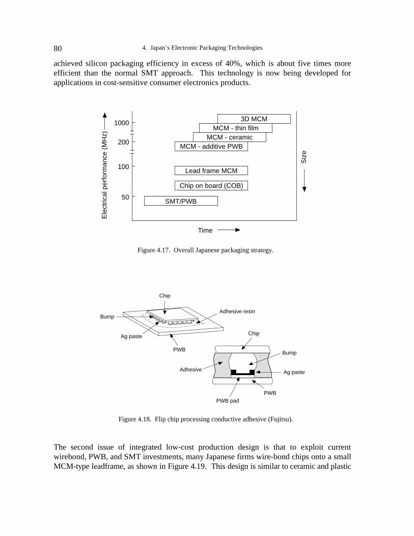
4. Japan’s Electronic Packaging Technologies80
achieved silicon packaging efficiency in excess of 40%, which is about five times moreefficient than the normal SMT approach. This technology is now being developed forapplications in cost-sensitive consumer electronics products.
~~
~~
200
100
50
1000
SMT/PWB
Chip on board (COB)
Lead frame MCM
MCM - additive PWBMCM - ceramic
MCM - thin film3D MCM
Siz
e
Ele
ctric
al p
erfo
rman
ce (
MH
z)
Time
Figure 4.17. Overall Japanese packaging strategy.
Chip
Bump
Ag paste
PWB
Adhesive resin
PWB pad
Adhesive
Chip
Bump
Ag paste
PWB
Figure 4.18. Flip chip processing conductive adhesive (Fujitsu).
The second issue of integrated low-cost production design is that to exploit currentwirebond, PWB, and SMT investments, many Japanese firms wire-bond chips onto a smallMCM-type leadframe, as shown in Figure 4.19. This design is similar to ceramic and plastic
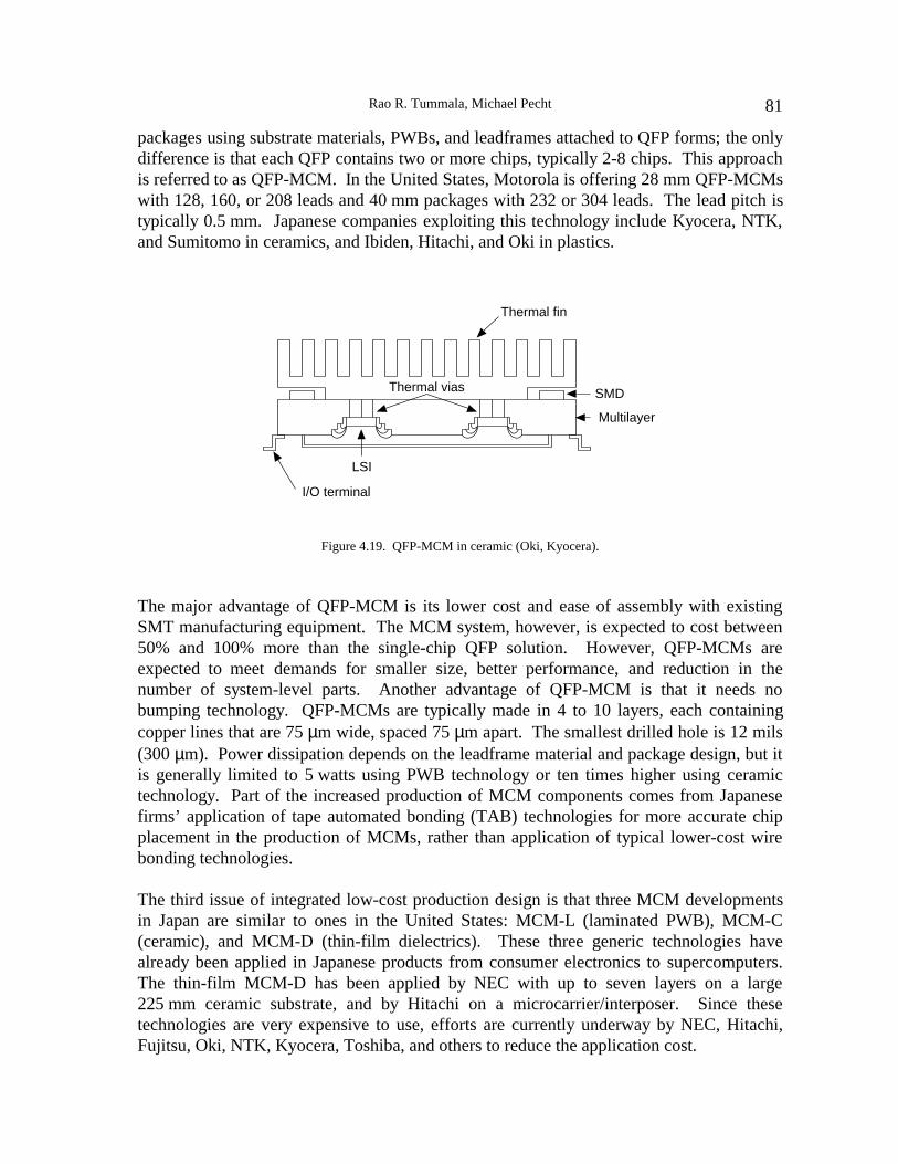
Rao R. Tummala, Michael Pecht 81
packages using substrate materials, PWBs, and leadframes attached to QFP forms; the onlydifference is that each QFP contains two or more chips, typically 2-8 chips. This approachis referred to as QFP-MCM. In the United States, Motorola is offering 28 mm QFP-MCMswith 128, 160, or 208 leads and 40 mm packages with 232 or 304 leads. The lead pitch istypically 0.5 mm. Japanese companies exploiting this technology include Kyocera, NTK,and Sumitomo in ceramics, and Ibiden, Hitachi, and Oki in plastics.
Thermal fin
SMD
LSI
Thermal vias
I/O terminal
Multilayer
Figure 4.19. QFP-MCM in ceramic (Oki, Kyocera).
The major advantage of QFP-MCM is its lower cost and ease of assembly with existingSMT manufacturing equipment. The MCM system, however, is expected to cost between50% and 100% more than the single-chip QFP solution. However, QFP-MCMs areexpected to meet demands for smaller size, better performance, and reduction in thenumber of system-level parts. Another advantage of QFP-MCM is that it needs nobumping technology. QFP-MCMs are typically made in 4 to 10 layers, each containingcopper lines that are 75 µm wide, spaced 75 µm apart. The smallest drilled hole is 12 mils(300 µm). Power dissipation depends on the leadframe material and package design, but itis generally limited to 5 watts using PWB technology or ten times higher using ceramictechnology. Part of the increased production of MCM components comes from Japanesefirms’ application of tape automated bonding (TAB) technologies for more accurate chipplacement in the production of MCMs, rather than application of typical lower-cost wirebonding technologies.
The third issue of integrated low-cost production design is that three MCM developmentsin Japan are similar to ones in the United States: MCM-L (laminated PWB), MCM-C(ceramic), and MCM-D (thin-film dielectrics). These three generic technologies havealready been applied in Japanese products from consumer electronics to supercomputers.The thin-film MCM-D has been applied by NEC with up to seven layers on a large225 mm ceramic substrate, and by Hitachi on a microcarrier/interposer. Since thesetechnologies are very expensive to use, efforts are currently underway by NEC, Hitachi,Fujitsu, Oki, NTK, Kyocera, Toshiba, and others to reduce the application cost.
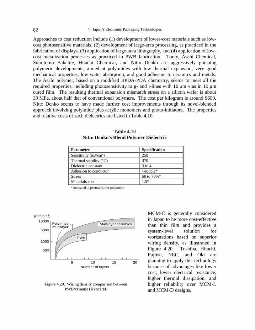
4. Japan’s Electronic Packaging Technologies82
Approaches to cost reduction include (1) development of lower-cost materials such as low-cost photosensitive materials, (2) development of large-area processing, as practiced in thefabrication of displays, (3) application of large-area lithography, and (4) application of low-cost metalization processes as practiced in PWB fabrication. Toray, Asahi Chemical,Sumitomo Bakelite, Hitachi Chemical, and Nitto Denko are aggressively pursuingpolymeric developments, aimed at polyimides with low thermal expansion, very goodmechanical properties, low water absorption, and good adhesion to ceramics and metals.The Asahi polymer, based on a modified BPDA-PDA chemistry, seems to meet all therequired properties, including photosensitivity to g- and i-lines with 10 µm vias in 10 µmcured film. The resulting thermal expansion mismatch stress on a silicon wafer is about30 MPa, about half that of conventional polymers. The cost per kilogram is around $600.Nitto Denko seems to have made further cost improvements through its novel-blendedapproach involving polyimide plus acrylic monomers and photo-initiators. The propertiesand relative costs of such dielectrics are listed in Table 4.10.
Table 4.10Nitto Denko's Blend Polymer Dielectric
Parameter SpecificationSensitivity (mJ/cm2) 250Thermal stability (°C) 370Dielectric constant 3 to 4Adhesion to conductor >double*Stress 60 to 70%*Materials cost 1.5*
*compared to photosensitive polyimide
MCM-C is generally consideredin Japan to be more cost-effectivethan thin film and provides asystem-level solution forworkstations based on superiorwiring density, as illustrated inFigure 4.20. Toshiba, Hitachi,Fujitsu, NEC, and Oki areplanning to apply this technologybecause of advantages like lowercost, lower electrical resistance,higher thermal dissipation, andhigher reliability over MCM-Land MCM-D designs.
PWB
Multilayer ceramicsPolyimidemultilayer
10000
5000
1000
500
(mm/cm2)
5 10 15 20Number of layers
Figure 4.20. Wiring density comparison betweenPWB/ceramic (Kyocera).

Rao R. Tummala, Michael Pecht 83
The primary advantage of ceramic over PWB (previously shown in Figure 4.11) is in thenumber of lines/vias per 100 mil channel, ceramic providing as many as 9 lines, each100 µm wide, compared with 5 lines in PWB. But the Japanese are driving bothtechnologies to much higher densities and to much lower costs. The technologyimprovements in PWB, however, come as process improvements as opposed to thedevelopment of parallel co-fire ceramic processes. Low-cost applications in VCRs andcamcorders are beginning to appear using ceramic technology. Panasonic, for example, isalready using its low-temperature ceramic components (LTCC) in peripheral tape memorysystems and is expected to further apply it in cellular, automotive, camcorder, andcomputer applications. By using the LTCC as a lead-array hybrid (1.0 mm pitch) withthrough-hole mounting onto a PWB, Panasonic found it to be less expensive than thetypical PWB approach. The embedded capacitors made of Pb(Mg1/3Nb2/3 )O3-PbTiO3-PbOprovide a capacitance of 30 nf/cm2. Canon camcorders have also used LTCC, presumablymanufactured by Kyocera.
MCMs based on PWB technology are expected to be the most dominant because of priorinvestments and the existing infrastructure in Japan. The PWB base is being enhanced by(1) new materials, such as aramid fiber, BT resin, maleimide styryl, and photosensitiveepoxy, (2) new processes such as additive plate and laser/photo vias, and (3) large-area,low-cost processing in not-so-clean facilities. These enhancements are in addition to thosebeing pursued in conventional subtractive processes. The chip assembly to form multichipmodules has already been practiced by direct wire bonding, TAB, and flip chip bonding ofbare die. The wire bonding experience comes from consumer product COB, and TAB isemployed in performance computers and consumer products. Flip chip is a recentintroduction by Hitachi in its mainframes, and by IBM (Japan) in its PC products, whereinbumped chip is solder-bonded to PWB using eutectic solder. In addition, Fujitsu isexploring the same with conductive epoxy, eliminating both Pb solder and flux. In 1994,Mitsubishi’s new cellular telephone used advanced flip chip assembly techniques.
PRINTED WIRING BOARD TECHNOLOGIES
Japan is enhancing printed wiring board (PWB) technology to meet market demands forlow-cost, thin, and lightweight consumer products. PWB enhancements fall into severalcategories:
• Thin and fine-line conventional subtractive etching process.
• Low-cost, fine line, thin film, additive process. Shown in Figure 4.21, this is a newsequential process involving deposition of photosensitive polymer or epoxy, formationof via holes by large-area photo exposure, and subsequent chemical etching andmetalization by catalytic chemical seeding and electroless plating. The advantages ofthis process are many, including pattern shape, pattern thickness control, pattern widthcontrol, mounting reliability, and most importantly, small via size. Ibiden compares thesubtractive and additive processes in Figure 4.21.
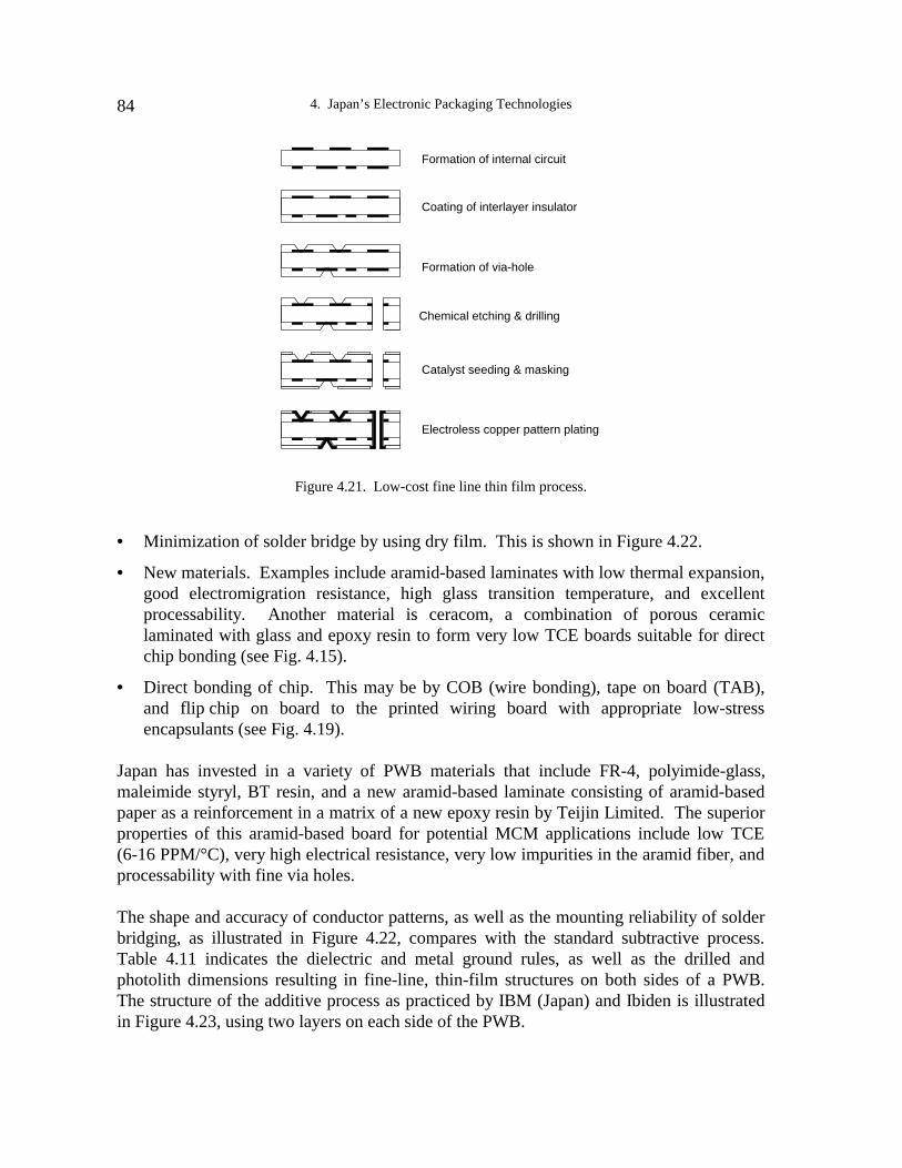
4. Japan’s Electronic Packaging Technologies84
Formation of internal circuit
Coating of interlayer insulator
Formation of via-hole
Chemical etching & drilling
Catalyst seeding & masking
Electroless copper pattern plating
Figure 4.21. Low-cost fine line thin film process.
• Minimization of solder bridge by using dry film. This is shown in Figure 4.22.
• New materials. Examples include aramid-based laminates with low thermal expansion,good electromigration resistance, high glass transition temperature, and excellentprocessability. Another material is ceracom, a combination of porous ceramiclaminated with glass and epoxy resin to form very low TCE boards suitable for directchip bonding (see Fig. 4.15).
• Direct bonding of chip. This may be by COB (wire bonding), tape on board (TAB),and flip chip on board to the printed wiring board with appropriate low-stressencapsulants (see Fig. 4.19).
Japan has invested in a variety of PWB materials that include FR-4, polyimide-glass,maleimide styryl, BT resin, and a new aramid-based laminate consisting of aramid-basedpaper as a reinforcement in a matrix of a new epoxy resin by Teijin Limited. The superiorproperties of this aramid-based board for potential MCM applications include low TCE(6-16 PPM/°C), very high electrical resistance, very low impurities in the aramid fiber, andprocessability with fine via holes.
The shape and accuracy of conductor patterns, as well as the mounting reliability of solderbridging, as illustrated in Figure 4.22, compares with the standard subtractive process.Table 4.11 indicates the dielectric and metal ground rules, as well as the drilled andphotolith dimensions resulting in fine-line, thin-film structures on both sides of a PWB.The structure of the additive process as practiced by IBM (Japan) and Ibiden is illustratedin Figure 4.23, using two layers on each side of the PWB.
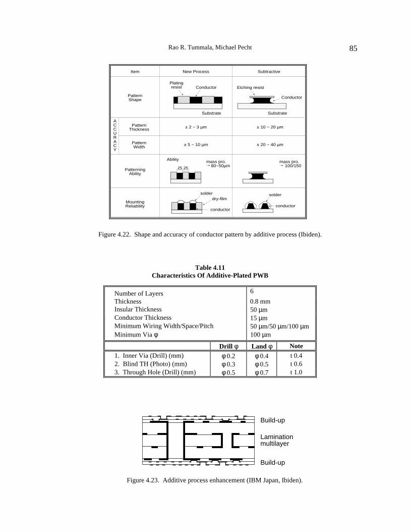
Rao R. Tummala, Michael Pecht 85
Platingresist Conductor
Substrate
Etching resist
Conductor
Ability mass pro. 80~50µm
mass pro. 100/150
solderdry-film
conductor
solder
conductor
25 25
Substrate
ACCURACY
Item New Process Subtractive
PatternShape
PatternThickness
PatternWidth
± 2 ~ 3 µm ± 10 ~ 20 µm
± 5 ~ 10 µm ± 20 ~ 40 µm
PatterningAbility
MountingReliability
Figure 4.22. Shape and accuracy of conductor pattern by additive process (Ibiden).
Table 4.11Characteristics Of Additive-Plated PWB
Number of Layers 6
Thickness 0.8 mm Insular Thickness 50 µm Conductor Thickness 15 µm Minimum Wiring Width/Space/Pitch 50 µm/50 µm/100 µm Minimum Via φ 100 µm
Drill φ Land φ Note 1. Inner Via (Drill) (mm) φ 0.2 φ 0.4 t 0.4 2. Blind TH (Photo) (mm) φ 0.3 φ 0.5 t 0.6 3. Through Hole (Drill) (mm) φ 0.5 φ 0.7 t 1.0
Build-up
Laminationmultilayer
Build-up
Figure 4.23. Additive process enhancement (IBM Japan, Ibiden).

4. Japan’s Electronic Packaging Technologies86
Conductive Adhesives
Conductive adhesives are alternatives to solder andbraze connections in chip and packaging assemblies.The concept shown in Figure 4.24 allows electricalconnection to be made as a result of the z-axisalignment of particles. Because of low cost andprocess simplicity, the technology is currently usedfor LCD connections. Conductive adhesives arebeing explored and applied by almost all majorJapanese consumer product companies. Thematerials typically consist of thermoplastic andthermoset materials that provide adhesion tosurrounding metallic particles, typically Ag solder;these are then applied as paste.
The conductive adhesive technology that includes a specialty technology referred to asanisotropic adhesive connection (ACA) is ideally suited for low-cost, lightweight, and low-profile applications. Examples of the use of this technology include (1) the connectionbetween an LCD driver IC and the display panel, as in Fujitsu’s notebook computer, and(2) the connection between a bumped chip and a PWB used by Fujitsu (see Fig. 4.19).A variation of the conductive adhesive used by Sharp in display modules uses sphericalpolymeric materials coated with nickel and gold, presumably by electroless plating. Such asystem provides stress relief in the conductive adhesive joint due to the low modulus ofcore organic particles, yet it provides the required electrical conduction.
Flex Circuits
Japan places very high priority on flex film technology, which it has used in cameras,connectors, and video games. It has also used this technology to connect ICs to LCDdisplays. Its advantages include 3-dimensional conformal nature, light weight, and thinfilm. There are several examples of direct chip on flex, as used in the wrist pager, makingpackages even more compact. Sharp is currently developing multilayer flex film for futureconsumer product applications.
CHIP ASSEMBLY TECHNOLOGIES
Japan is practicing chip assembly in more ways than does the United States. It is pushingwire bonding to its limits and is highly successful in the use of TAB, having applied it fromconsumer to supercomputer packaging. The Japanese have applied and continue to applyflip chip both with solder and with conductive adhesive technologies. In addition, they arecontinuing to push chip on board, not only by wire bonding the chip to the board, but alsoby TAB bonding to board and flip chip solder bonding to organic board. In a newdevelopment Fujitsu is offering its BIT system for notebook computer applications.
Conductive trace Insulative adhesive
Flexible printed circuit
Z-axis filled adhesive
Conductive trace
Printed circuit board
Flexible printed circuit
Printed circuit board
Heat & pressure
Figure 4.24. Anisotropic conductiveconductor system.
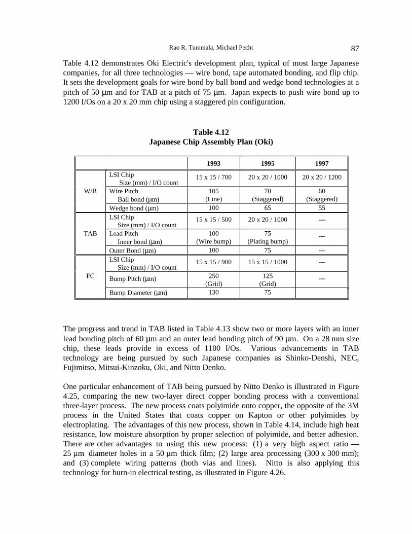
Rao R. Tummala, Michael Pecht 87
Table 4.12 demonstrates Oki Electric's development plan, typical of most large Japanesecompanies, for all three technologies — wire bond, tape automated bonding, and flip chip.It sets the development goals for wire bond by ball bond and wedge bond technologies at apitch of 50 µm and for TAB at a pitch of 75 µm. Japan expects to push wire bond up to1200 I/Os on a 20 x 20 mm chip using a staggered pin configuration.
Table 4.12Japanese Chip Assembly Plan (Oki)
1993 1995 1997
LSI Chip Size (mm) / I/O count
15 x 15 / 700 20 x 20 / 1000 20 x 20 / 1200
W/B Wire Pitch Ball bond (µm)
105(Line)
70(Staggered)
60(Staggered)
Wedge bond (µm) 100 65 55LSI Chip Size (mm) / I/O count
15 x 15 / 500 20 x 20 / 1000 ---
TAB Lead Pitch Inner bond (µm)
100(Wire bump)
75(Plating bump)
---
Outer Bond (µm) 100 75 ---LSI Chip Size (mm) / I/O count
15 x 15 / 900 15 x 15 / 1000 ---
FC Bump Pitch (µm) 250(Grid)
125(Grid)
---
Bump Diameter (µm) 130 75
The progress and trend in TAB listed in Table 4.13 show two or more layers with an innerlead bonding pitch of 60 µm and an outer lead bonding pitch of 90 µm. On a 28 mm sizechip, these leads provide in excess of 1100 I/Os. Various advancements in TABtechnology are being pursued by such Japanese companies as Shinko-Denshi, NEC,Fujimitso, Mitsui-Kinzoku, Oki, and Nitto Denko.
One particular enhancement of TAB being pursued by Nitto Denko is illustrated in Figure4.25, comparing the new two-layer direct copper bonding process with a conventionalthree-layer process. The new process coats polyimide onto copper, the opposite of the 3Mprocess in the United States that coats copper on Kapton or other polyimides byelectroplating. The advantages of this new process, shown in Table 4.14, include high heatresistance, low moisture absorption by proper selection of polyimide, and better adhesion.There are other advantages to using this new process: (1) a very high aspect ratio —25 µm diameter holes in a 50 µm thick film; (2) large area processing (300 x 300 mm);and (3) complete wiring patterns (both vias and lines). Nitto is also applying thistechnology for burn-in electrical testing, as illustrated in Figure 4.26.
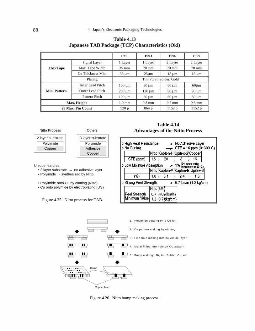
4. Japan’s Electronic Packaging Technologies88
Table 4.13Japanese TAB Package (TCP) Characteristics (Oki)
Figure 4.26. Nitto bump making process.
1990 1993 1996 1999
Signal Layer 1 Layer 1 Layer 2 Layer 2 Layer
TAB Tape Max. Tape Width 35 mm 70 mm 70 mm 70 mm
Cu Thickness Min. 35 µm 25µm 18 µm 18 µm
Plating Tin, Pb/Sn Solder, Gold
Inner Lead Pitch 100 µm 80 µm 60 µm 60µm
Min. Pattern Outer Lead Pitch 200 µm 120 µm 90 µm 90 µm
Pattern Pitch 100 µm 80 µm 60 µm 60 µm
Max. Height 1.0 mm 0.8 mm 0.7 mm 0.6 mm
28 Max. Pin Count 520 p 864 p 1152 p 1152 p
Nitto Process Others
2 layer substrate
PolyimideCopper
3 layer substrate
PolyimideAdhesiveCopper
Unique features: • 2 layer substrate → no adhesive layer • Polyimide → synthesized by Nitto
• Polyimide onto Cu by coating (Nitto) • Cu onto polymide by electroplating (US)
Figure 4.25. Nitto process for TAB.
Table 4.14Advantages of the Nitto Process
Bump
Copper lead
1. Polyimide coating onto Cu foi l
2. Cu pattern making by etching
3. Fine hole making into polyimide layer
4. Metal f i l l ing into hole on CU pattern
5. Bump making: Ni, Au, Solder, Cu, etc.

Rao R. Tummala, Michael Pecht 89
Flip chip technology is being extensively studied by almost all major Japanese firms and isalready used in products by Hitachi and IBM (Japan). The Hitachi flip chip, together withmicrocarrier BGA assembly to next-level package (mullite glass-ceramic), is illustrated inFigure 4.27. The microcarrier, which is only bigger than the chip itself by about 2 mm, is asingle-chip carrier fabricated with seven-layer mullite ceramic and five levels of polyimide-aluminum thin-film technology. Flip chip enhancements being pursued by Japaneseelectronic companies generally consist of one of two approaches — solder bonding(including Pb-Sn, Pb-In), and conductor adhesive bonding. Bump technology itself, likeFujitsu’s bump integration technology (BIT), is generating considerable interest. Oneexample is illustrated in Figure 4.28 using thin-film and electroplating processes. Incontrast, the Germans are pursuing electroless-plate bumping, while the British are tryinggold ball bumping by wire-bonding tools.
The flip chip bonding receiving the greatest interest in Japan is the technology IBM (Japan)pioneered as an extension of IBM (U.S.) flip chip technology developed three decades ago.It involves direct bonding of a bumped chip to a PWB by the use of low- temperaturesolder that is hot-injection-deposited onto PWB through a mask. The challenge here is todevelop a thermally compatible encapsulant to reduce the strain on the solder joint arisingfrom the great mismatch in thermal expansions between PWB (17 PPM) and chip (3 PPM).
Figure 4.29 illustrates a tenfold strain reduction when the encapsulant is used between thePWB and the chip. This discovery has major implications for the Japanese packagingindustry, particularly for consumer electronics, as it allows Japanese investments in PWBto be incrementally improved over the next decade. Figure 4.30 shows the eutectic solderto be more effective than high-Pb solder (95/5) in achieving the desired fatigue life.
Japanese manufacturers have used and continue to use chip-on-board technology usingwire bond to PWB.
LSI chip
Multilite ceramic base board(7 conductor layers)
AIN cap
Soldered
Soldered seal
Solder bump(minimum
250 µm pitch)
Thin film layers(5 wiring layers, 1
resistor layer)
Solder bump(450 µm pitch)
Figure 4.27. Microprocessor carrier (BGA) for LSI(Hitachi).
Au Pad
Wafer
Au/Ti
Bump
Photoresist
Figure 4.28. Bump fabricationprocess (Sharp).

4. Japan’s Electronic Packaging Technologies90
PACKAGE ASSEMBLY TECHNOLOGIES
Package assembly involves attaching components to the next-level assembly, usuallyprinted wiring boards. Assembly includes active plastic and ceramic componentscontaining logic and memory chips as well as nonactive components like capacitors,resistors, and inductors. The assembly itself involves either surface mount or pin-through-hole (PTH) attachment. PTH is expensive, space-consuming, and heavy compared toSMT. Given the need for both low cost and portability in consumer products, Japan hasinvested very heavily in and has continually improved the technology to achieve assemblydensities of 20 components/cm2 as in Sony’s Video TR-5, based on 0.5 mm QFP pitch andpassive component sizes of 1.0 x 0.5 mm. This trend in increasing density is illustrated inFigure 4.31 for notebooks, palmtops, cellular phones, organizers, and camcorders.Assembly density in Japan is expected to reach 50 components/cm2 by the year 2000.
Without encapsulation
With encapsulation
0 40 80 120 160 200 220
10
8
6
4
2
0
Str
ain
(%
)
Joint height (micron)
Figure 4.29. Effects of encapsulation on strain insolder (IBM Japan).
Without encapsulation, 5/95 and 63/37 solders
With encapsulation, 5/95 solder
With encapsulation, 63/37 solder
12
10
8
6
4
2
Str
ain
(%)
0%63/37
25%63/37
50%63/37
75%63/37
100%63/37
Solder Composition
Figure 4.30. Effects of encapsulation and solder composition on strain in solder (IBM Japan).
Camcorder (1993)Cellular phone (1993)Palm top (1993)Notebook (1993)
Camcorder(2000)
Tren
d
1980 1985 1990 1995 2000
40
20
10
30
Com
pone
nts/
cm2
50
Year
Figure 4.31. Japanese consumer product component density trend (Sony).

Rao R. Tummala, Michael Pecht 91
Consumer products require thin and lightweight packaging. Plastic packages such as QFPthat are surface-mounted onto PWB have effectively met consumer product requirements.The Japanese vision of next-generation products requires packages that are smaller andcheaper than in the past, roughly 50% smaller for each new generation. Given Japan's pastinvestments in PWB and SMT technologies, and given increased global cost-competitivepressures, Japan is expected to pursue the use of plastic packages to the ultimate limit. Theultimate limit accepted by Japan currently is 0.15 mm leadframe pitch, giving rise to 800pins in 30 mm2 and 1000 pins in 38 mm2 sizes.
The continued use of P-QFP beyond the current 0.4 mm pitch toward 0.15 mm pitch,however, requires major enhancements in SMT pick and placement tools, solder depositiontechnologies, reflow tools and technologies, inspection, solder repair for opens and shorts,and electromigration resistance of both the plastic package and the printed wiring board.Contrary to what U.S. companies might expect, Japanese industry will incrementallyenhance each of these to a level that will guarantee high yield and high reliability. Thisconclusion is supported by (1) Sony’s advancements in factory automation and (2) Oki’ssingle-PPM-defect-soldering systems. These systems and processes have loweredassembly defects to less than 20 PPM, as shown in Figure 4.32. Sony’s precision robotshave improved placement repeatability to 0.01 mm from 0.05 mm during the last six years.Matsushita’s new SMT machine has 11 placement heads with 0.01 mm repeatability.Toshiba’s advanced TAB equipment can place 0.2 mm pitch parts using CCD vision, sincepitch size has reached the limits of human vision.
1.5
1.0
0.5
Soldering atmosphereTotal PWBsDefect PWBs
Failure rate per PWB (%)
Solder bridge 0.57
0.63%
0.02%
Air (1992.7)18,506 PWBs
117 PWBs
N2 (1992.9)21,002 PWBs
4 PWBs
Figure 4.32. Soldering defect improvement achieved at Oki.
With increased miniaturization, soldering technologies continue to evolve. For example,Oki’s single PPM defect technology includes developments in the following:
• new wave soldering machine for zero defects
• nitrogen flow soldering process technology
• rheology and printability of solder paste
• inspection technique for solder paste printability and printing parameter optimization
• development of an automatic solder-joint inspection system
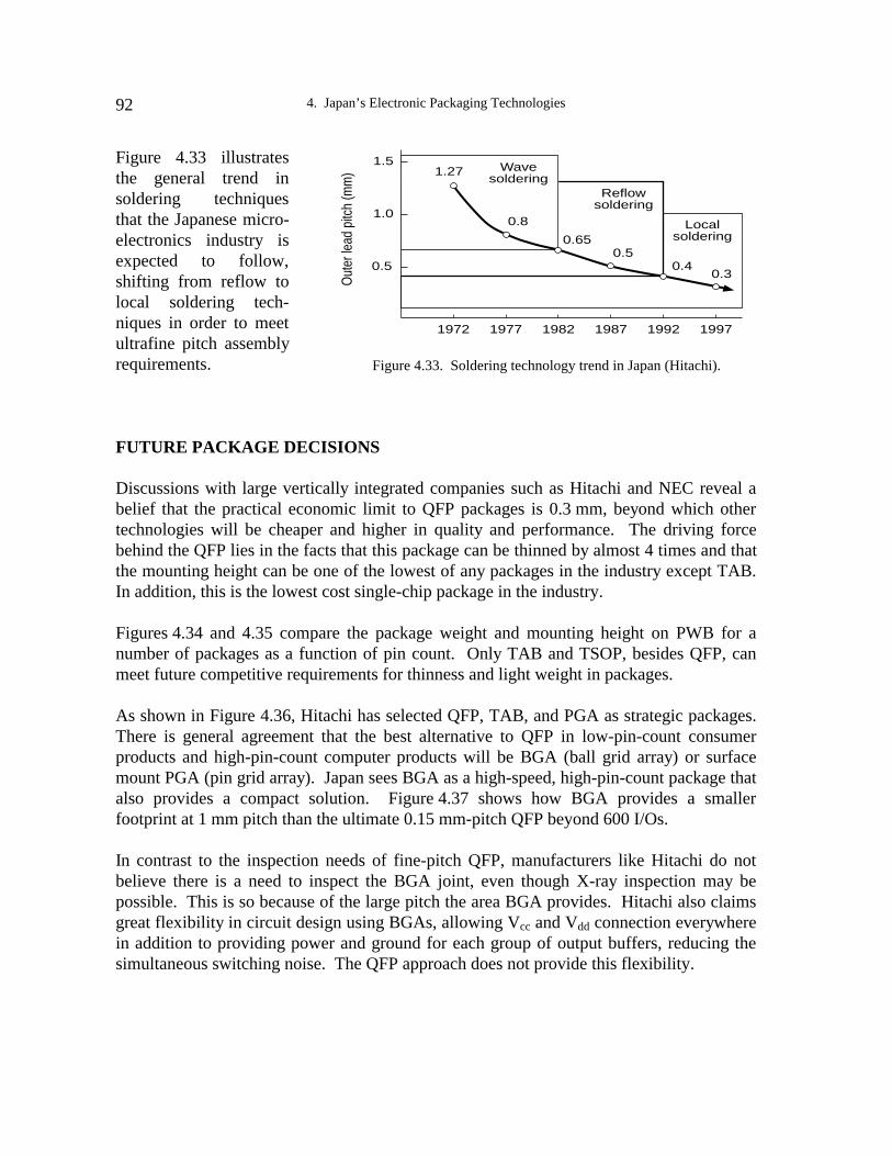
4. Japan’s Electronic Packaging Technologies92
Figure 4.33 illustratesthe general trend insoldering techniquesthat the Japanese micro-electronics industry isexpected to follow,shifting from reflow tolocal soldering tech-niques in order to meetultrafine pitch assemblyrequirements.
FUTURE PACKAGE DECISIONS
Discussions with large vertically integrated companies such as Hitachi and NEC reveal abelief that the practical economic limit to QFP packages is 0.3 mm, beyond which othertechnologies will be cheaper and higher in quality and performance. The driving forcebehind the QFP lies in the facts that this package can be thinned by almost 4 times and thatthe mounting height can be one of the lowest of any packages in the industry except TAB.In addition, this is the lowest cost single-chip package in the industry.
Figures 4.34 and 4.35 compare the package weight and mounting height on PWB for anumber of packages as a function of pin count. Only TAB and TSOP, besides QFP, canmeet future competitive requirements for thinness and light weight in packages.
As shown in Figure 4.36, Hitachi has selected QFP, TAB, and PGA as strategic packages.There is general agreement that the best alternative to QFP in low-pin-count consumerproducts and high-pin-count computer products will be BGA (ball grid array) or surfacemount PGA (pin grid array). Japan sees BGA as a high-speed, high-pin-count package thatalso provides a compact solution. Figure 4.37 shows how BGA provides a smallerfootprint at 1 mm pitch than the ultimate 0.15 mm-pitch QFP beyond 600 I/Os.
In contrast to the inspection needs of fine-pitch QFP, manufacturers like Hitachi do notbelieve there is a need to inspect the BGA joint, even though X-ray inspection may bepossible. This is so because of the large pitch the area BGA provides. Hitachi also claimsgreat flexibility in circuit design using BGAs, allowing Vcc and Vdd connection everywherein addition to providing power and ground for each group of output buffers, reducing thesimultaneous switching noise. The QFP approach does not provide this flexibility.
1972 1977 1982 1987 1992 1997
1.5
1.0
0.5
Out
er le
ad p
itch
(mm
)
Reflow soldering
Wave soldering
Local soldering
1.27
0.8
0.650.5
0.40.3
Figure 4.33. Soldering technology trend in Japan (Hitachi).
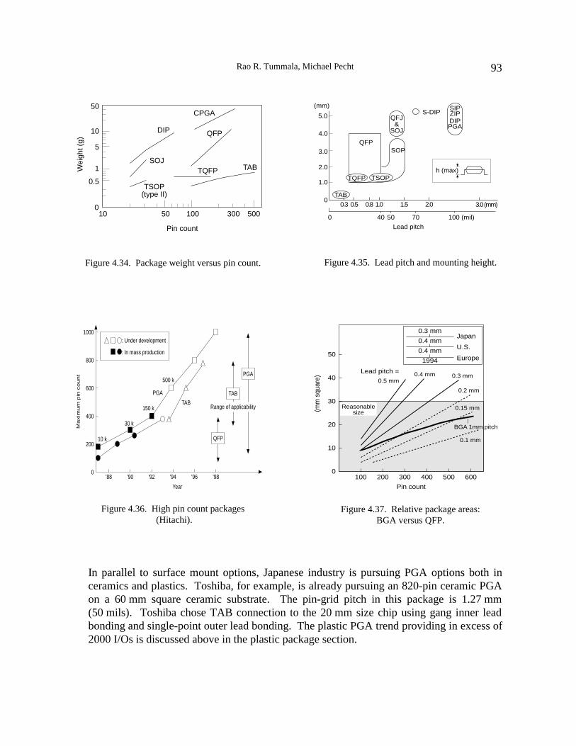
Rao R. Tummala, Michael Pecht 93
In parallel to surface mount options, Japanese industry is pursuing PGA options both inceramics and plastics. Toshiba, for example, is already pursuing an 820-pin ceramic PGAon a 60 mm square ceramic substrate. The pin-grid pitch in this package is 1.27 mm(50 mils). Toshiba chose TAB connection to the 20 mm size chip using gang inner leadbonding and single-point outer lead bonding. The plastic PGA trend providing in excess of2000 I/Os is discussed above in the plastic package section.
10 k
30 k
150 k
500 k
: Under development
: In mass production
TAB
PGA
QFP
TAB
PGA
Range of applicability
'88 '90 '92 '94 '96 '98
1000
800
600
400
200
0
Ma
xim
um
pin
co
un
t
Year
Figure 4.36. High pin count packages (Hitachi).
Lead pitch =0.5 mm
0.4 mm 0.3 mm
0.2 mm
0.15 mm
0.1 mm
BGA 1mm pitch
Reasonablesize
50
40
30
20
10
0100 200 300 400 500 600
(mm
squ
are)
Pin count
Japan
U.S.
Europe
0.3 mm
0.4 mm
0.4 mm
1994
Figure 4.37. Relative package areas:BGA versus QFP.
SOJ
TSOP(type II)
DIP
CPGA
QFP
TQFP TAB
5010 100 300 500
50
10
5
1
0.5
0
Pin count
Wei
ght (
g)
Figure 4.34. Package weight versus pin count.
TAB
TQFP TSOP
SOPQFP
S-DIPQFJ
&SOJ
DIPPGA
SIPZIP
h (max)
0.3 0.5 0.8 1.0 1.5 2.0 3.0 (mm)
100 (mil)7050400
0
1.0
2.0
3.0
4.0
5.0
Lead pitch
(mm)
Figure 4.35. Lead pitch and mounting height.

4. Japan’s Electronic Packaging Technologies94
Figure 4.38 summarizes the overall Japanese packaging assembly trend, illustrating thinquad flat pack (TQFP) as its main thrust, with TAB and PGA as parallel thrusts. The BGAis expected in applications requiring over 400-600 I/Os. Beyond the miniaturization ofQFP technologies, Japanese firms continue to develop chip on board, tape automatedbonding, and flip chip technologies to meet increasing packaging density futurerequirements, as shown in Figure 4.39.
CrossSection
Packagingdensity
Technology SMT/PWB
Low
COB TOB (TAB) Flip chip
Low ~ Medium Medium ~ High High
Time Today Future
Figure 4.39. Japanese packaging assembly strategy (Sharp).
1990 1992 1994 1996 1998 2000 2002
1000
800
600
400
200
0
Pin
cou
nt
Year
BGA
TQFP
C-PGA
QFP
Figure 4.38. Japanese high pin count strategy (Oki).

Rao R. Tummala, Michael Pecht 95
SUMMARY OF JAPANESE PACKAGING TRENDS
A summary of the Japanese electronic packaging roadmaps is listed in Table 4.15,indicating the expected advancements in component-mounting density, semiconductorpackaging, passive component size, and second-level organic/inorganic board technologies.
Table 4.15Japanese Packaging Technology Trends
1985 1990 1995 2000
Mounting form Single side Both sides Bare chipMixed mounting
Thin and thick3D mounting
Mounting density/cm2 5-10 15 20 50
Parts:- Semiconductor
- Passives
DIP SOP
--3.2 x 1.6 mm
QFP100-200 pin0.8 x 0.65 mm2.1 x 1.25 mm
TAB300-500 pin0.5 x 0.3 mm1.0 x 0.5 mm
MultichipmoduleModule withbuilt-in C, R, L
Basic board:- Organic
- Ceramic
One side print150 µ lines
AluminaW
4 layer100 µ lines
Glass ± ceramicAg-Pd conductor
6 layer80 µ lines
Low dielectric constantGlass + ceramicCu conductorAlN/W
10 layer50 µ linesBuilt-in C, RBuilt-in C, R
CONCLUSION
A graphic comparison of Japanese and U.S. electronic packaging technologies may befound in Table E.1 of the Executive Summary, page xviii. This table clearly shows thatJapan leads the United States in almost every category.
The JTEC panel maintains that much of Japan's advantage comes from its focus on high-volume production technologies that force the extension of existing technologies to keepcosts down. In the future, we can expect to see these advantages applied to more of ourtraditional industrial markets where smaller volumes have been typical. Lack of basicpackaging technologies will lead to loss of U.S. industries unless corrective action is taken.
REFERENCES
Microelectronics and Computer Technology Corporation and Sandia National Laboratory(MCC/Sandia). 1993. Industrial Competitiveness in the Balance: A Net TechnicalAssessment of North American vs. Offshore Electronics Packaging Technology. (U.S.Department of Energy Contract #AD-3474.)

4. Japan’s Electronic Packaging Technologies96
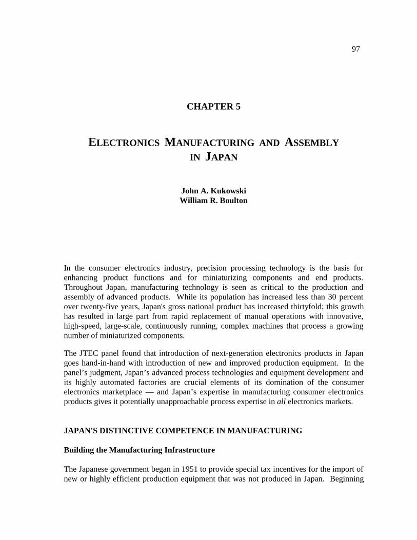
97
CHAPTER 5
ELECTRONICS MANUFACTURING AND ASSEMBLY
IN JAPAN
John A. KukowskiWilliam R. Boulton
In the consumer electronics industry, precision processing technology is the basis forenhancing product functions and for miniaturizing components and end products.Throughout Japan, manufacturing technology is seen as critical to the production andassembly of advanced products. While its population has increased less than 30 percentover twenty-five years, Japan's gross national product has increased thirtyfold; this growthhas resulted in large part from rapid replacement of manual operations with innovative,high-speed, large-scale, continuously running, complex machines that process a growingnumber of miniaturized components.
The JTEC panel found that introduction of next-generation electronics products in Japangoes hand-in-hand with introduction of new and improved production equipment. In thepanel’s judgment, Japan’s advanced process technologies and equipment development andits highly automated factories are crucial elements of its domination of the consumerelectronics marketplace — and Japan’s expertise in manufacturing consumer electronicsproducts gives it potentially unapproachable process expertise in all electronics markets.
JAPAN'S DISTINCTIVE COMPETENCE IN MANUFACTURING
Building the Manufacturing Infrastructure
The Japanese government began in 1951 to provide special tax incentives for the import ofnew or highly efficient production equipment that was not produced in Japan. Beginning
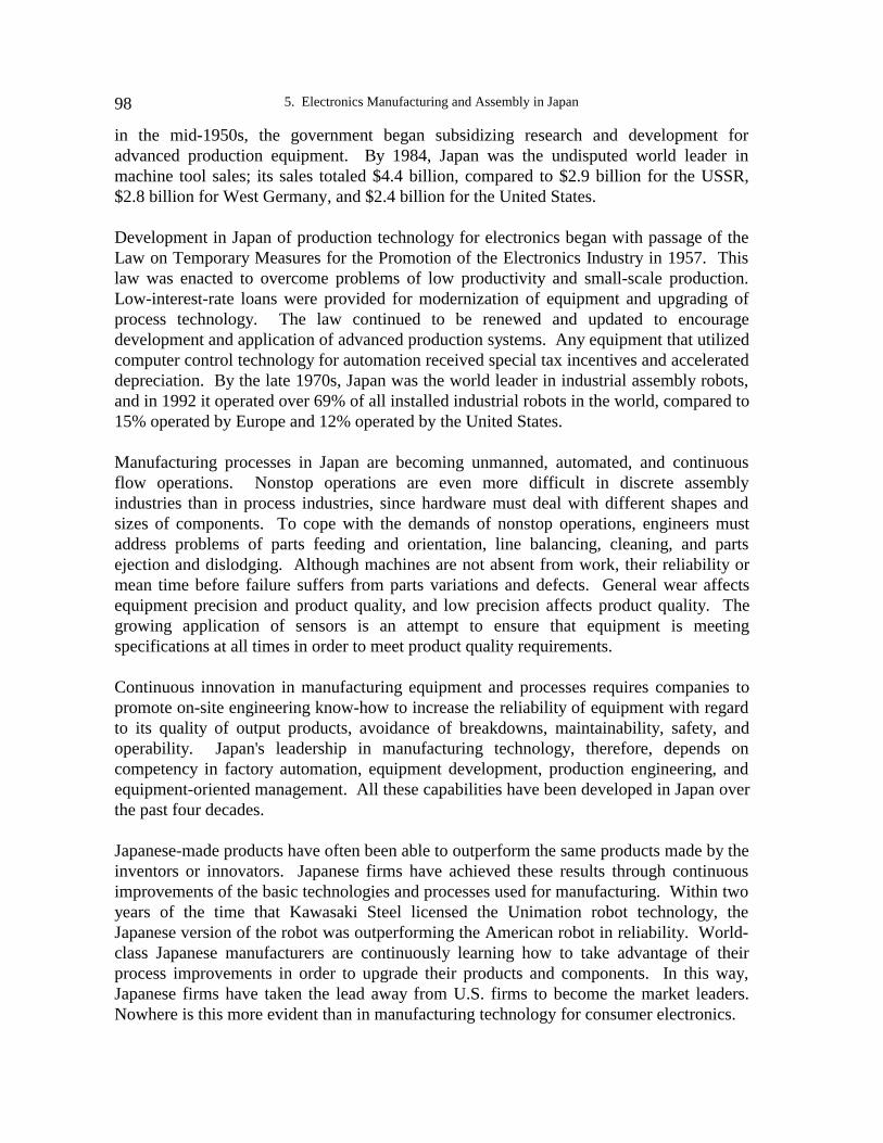
5. Electronics Manufacturing and Assembly in Japan98
in the mid-1950s, the government began subsidizing research and development foradvanced production equipment. By 1984, Japan was the undisputed world leader inmachine tool sales; its sales totaled $4.4 billion, compared to $2.9 billion for the USSR,$2.8 billion for West Germany, and $2.4 billion for the United States.
Development in Japan of production technology for electronics began with passage of theLaw on Temporary Measures for the Promotion of the Electronics Industry in 1957. Thislaw was enacted to overcome problems of low productivity and small-scale production.Low-interest-rate loans were provided for modernization of equipment and upgrading ofprocess technology. The law continued to be renewed and updated to encouragedevelopment and application of advanced production systems. Any equipment that utilizedcomputer control technology for automation received special tax incentives and accelerateddepreciation. By the late 1970s, Japan was the world leader in industrial assembly robots,and in 1992 it operated over 69% of all installed industrial robots in the world, compared to15% operated by Europe and 12% operated by the United States.
Manufacturing processes in Japan are becoming unmanned, automated, and continuousflow operations. Nonstop operations are even more difficult in discrete assemblyindustries than in process industries, since hardware must deal with different shapes andsizes of components. To cope with the demands of nonstop operations, engineers mustaddress problems of parts feeding and orientation, line balancing, cleaning, and partsejection and dislodging. Although machines are not absent from work, their reliability ormean time before failure suffers from parts variations and defects. General wear affectsequipment precision and product quality, and low precision affects product quality. Thegrowing application of sensors is an attempt to ensure that equipment is meetingspecifications at all times in order to meet product quality requirements.
Continuous innovation in manufacturing equipment and processes requires companies topromote on-site engineering know-how to increase the reliability of equipment with regardto its quality of output products, avoidance of breakdowns, maintainability, safety, andoperability. Japan's leadership in manufacturing technology, therefore, depends oncompetency in factory automation, equipment development, production engineering, andequipment-oriented management. All these capabilities have been developed in Japan overthe past four decades.
Japanese-made products have often been able to outperform the same products made by theinventors or innovators. Japanese firms have achieved these results through continuousimprovements of the basic technologies and processes used for manufacturing. Within twoyears of the time that Kawasaki Steel licensed the Unimation robot technology, theJapanese version of the robot was outperforming the American robot in reliability. World-class Japanese manufacturers are continuously learning how to take advantage of theirprocess improvements in order to upgrade their products and components. In this way,Japanese firms have taken the lead away from U.S. firms to become the market leaders.Nowhere is this more evident than in manufacturing technology for consumer electronics.
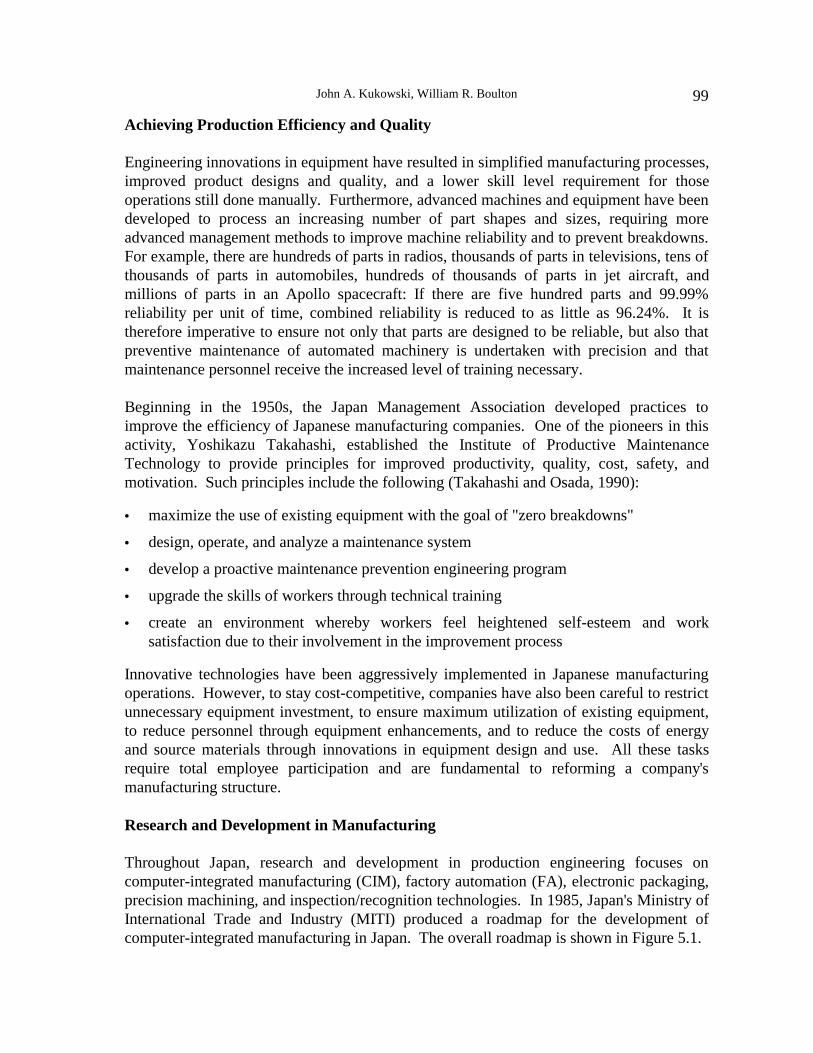
John A. Kukowski, William R. Boulton 99
Achieving Production Efficiency and Quality
Engineering innovations in equipment have resulted in simplified manufacturing processes,improved product designs and quality, and a lower skill level requirement for thoseoperations still done manually. Furthermore, advanced machines and equipment have beendeveloped to process an increasing number of part shapes and sizes, requiring moreadvanced management methods to improve machine reliability and to prevent breakdowns.For example, there are hundreds of parts in radios, thousands of parts in televisions, tens ofthousands of parts in automobiles, hundreds of thousands of parts in jet aircraft, andmillions of parts in an Apollo spacecraft: If there are five hundred parts and 99.99%reliability per unit of time, combined reliability is reduced to as little as 96.24%. It istherefore imperative to ensure not only that parts are designed to be reliable, but also thatpreventive maintenance of automated machinery is undertaken with precision and thatmaintenance personnel receive the increased level of training necessary.
Beginning in the 1950s, the Japan Management Association developed practices toimprove the efficiency of Japanese manufacturing companies. One of the pioneers in thisactivity, Yoshikazu Takahashi, established the Institute of Productive MaintenanceTechnology to provide principles for improved productivity, quality, cost, safety, andmotivation. Such principles include the following (Takahashi and Osada, 1990):
• maximize the use of existing equipment with the goal of "zero breakdowns"
• design, operate, and analyze a maintenance system
• develop a proactive maintenance prevention engineering program
• upgrade the skills of workers through technical training
• create an environment whereby workers feel heightened self-esteem and worksatisfaction due to their involvement in the improvement process
Innovative technologies have been aggressively implemented in Japanese manufacturingoperations. However, to stay cost-competitive, companies have also been careful to restrictunnecessary equipment investment, to ensure maximum utilization of existing equipment,to reduce personnel through equipment enhancements, and to reduce the costs of energyand source materials through innovations in equipment design and use. All these tasksrequire total employee participation and are fundamental to reforming a company'smanufacturing structure.
Research and Development in Manufacturing
Throughout Japan, research and development in production engineering focuses oncomputer-integrated manufacturing (CIM), factory automation (FA), electronic packaging,precision machining, and inspection/recognition technologies. In 1985, Japan's Ministry ofInternational Trade and Industry (MITI) produced a roadmap for the development ofcomputer-integrated manufacturing in Japan. The overall roadmap is shown in Figure 5.1.

5. Electronics Manufacturing and Assembly in Japan100
Introduction of computers in
factories
Computer AidedDesign
AutomaticWarehousing
System
ProductionManagementSystem
Design/ManufacturingSupportingSystem
AutomatedManufacturingSystem
MachineTools
MaterialsHandlingSystem
Computer AidedEngineering
Computer AidedEngineering
Integrationof software
IntegratedManagement
System
Computer Integrated
ManufacturingNC DNC CNC
Robots
FMS AdvancedFMS
Figure 5.1. Japan’s development of computer-integrated manufacturing ( MITI).
Computer-Integrated Manufacturing. In 1985, the Japanese initiated a project to develop astandard protocol for factory automation. The International Robotics and FactoryAutomation Association was established that year for the purpose of setting the standardfor communication between equipment used on the factory floor. The approach, calledminiMAP, was based on the lower four levels of the MAP manufacturing automationprotocol introduced by General Motors in the 1980s. The first prototype demonstrationswere made in 1992 and 1993 at the Japan Exhibition Center at Makuhari Messe, whereover twenty equipment makers demonstrated factory integration of their equipment usingthe miniMAP standard protocol. To quote Hitachi’s literature, "CIM is the only technologycapable of handling the explosive diversification of consumer goods in today's fast-pacedmarket environment driven by increasingly shorter concept to finished product."
The development of Japan's factory automation capabilities began with Toyota's prototypeintegrated factory in 1972. In 1978, MITI initiated a national R&D project to develop aflexible manufacturing factory, which was demonstrated in 1985 at MITI's mechanicalengineering laboratory in Tsukuba. The problem of standardizing the communication
John A. Kukowski, William R. Boulton 101
interface between equipment vendors was then addressed by the International Robotics andFactory Automation Association. By 1990, Japan was the world leader in installed flexiblemanufacturing system (FMS) lines and industrial robots and was working to develop fullCAD/CAM (computer-assisted design/manufacturing) capabilities for computer-integratedmanufacturing. FANUC, a major supplier of industrial robots and control systems forGeneral Motors, began implementing full CAD/CAM capabilities for its own factoryautomation in the late-1980s.
Leading Japanese electronic manufacturing and assembly companies have developed theirown advanced production and computer-integrated manufacturing capabilities. In-housecapability protects intellectual property, assures timely delivery, reduces costs, and reducesresponse times required for new product introductions. Such capabilities provide theJapanese with self-reliance and the ability to implement real "concurrent engineering"methodologies. Most companies, however, are selling their proprietary manufacturingtechnology in the open market in order to increase the return on their equipmentinvestment. The availability of the equipment in the open market is usually preceded bylong periods of utilization in Japanese facilities. Sony demonstrated to the JTEC panel afull range of production and assembly equipment developed for component manufacturingand final assembly applications. Sony's equipment sales now represent 2% of thecompany's sales. In the United States Polaroid Corporation has installed a completeassembly line that uses over 100 Sony robots.
Production Engineering Capabilities
Production technology is a key strength of Japanese firms. Most leaders in the electronicsindustry have established separate organizations to manage developments in productiontechnology. Their goals are to maximize manufacturing efficiency and high-quality output.On a corporate level, production engineering research laboratories provide the critical linkbetween product development and the development and application of advancedproduction equipment and processes. Every major business unit within a firm has its ownproduction engineering staff and production engineering laboratory to develop processdesign and process technology. Production technology development drives concurrentequipment, component, and product developments — final product design anddevelopment are synchronized with production technology development. The importanceof production engineering in Japanese firms is demonstrated by the fact that in companieslike Hitachi and NEC the production engineering departments report directly to thecompany presidents, alongside the other company research laboratories.
Most leading Japanese electronics companies also have materials characterizationlaboratories. Expertise in both materials and manufacturing processes guarantees high-quality outputs and improved reliability. It was evident to JTEC panelists that in Japanboth are the focus of attention when quality or reliability problems occur; likewise,improvements in materials, package architectures, and manufacturing processes remove thefailure causes.
5. Electronics Manufacturing and Assembly in Japan102
Equipment Development Capabilities
Without exception, every company visited by the JTEC panel has its own equipmentdevelopment teams for designing and building production equipment. Sony's factoryautomation and precision products group includes a thousand members. The FA systemsdivision makes advanced equipment to manufacture new products developed within Sony.The robotics and FA components division developed Sony's Multi Assembly RobotTechnology (SMART) systems. In addition, Sony has another three hundred peopleworking within the machine tool, production technology, and production engineeringdivisions to develop production systems for customers. In 1993, Nippondenso, Japan'sleading auto electronics firm, has over two hundred people at its Kota site to developproduction equipment and processes. This commitment has led to advanced productionsystems. Nippondenso’s main four-story building at Kota handles chip assembly, hybridmanufacturing, SMT board, and also final assembly, burn-in, and testing for more than 120models of engine controllers on one 100-meter manufacturing line. The production linewas replaced or upgraded every three to four years. Most of the Kota plant's equipment hasbeen produced in-house. JTEC panel members have never seen such levels of commitmentto process development in U.S. electronics firms.
Japanese industry as a whole has focused massive resources on the design and developmentof complex automated equipment, and the range of equipment development expertisewithin individual companies is tremendous. That expertise covers all the technologicalareas required to be self-sufficient and dominant in electronics manufacturing. Theconsensus in Japan is that equipment provides a major competitive advantage and thatequipment development technology is mandatory in order to lead in the introduction ofnew products. Japanese drivers for equipment development include cost reduction,machine accuracy, reliability, speed, flexibility, peripheral integration, ease of operation,and links to CAD (CAD-CAM integration). Numerous Japanese companies areaggressively producing and marketing electronics manufacturing equipment worldwide.
Equipment Development Teams. The Japanese approach to equipment development isbuilt on the team concept. Numerous individuals with varied technical backgrounds areteamed together during the development process. Members of the development team areultimately transferred to the manufacturing facility for implementation and to continueequipment enhancements to maximize production efficiency. This ensures highly skilledtechnical personnel to operate, maintain, and continuously implement changes required toenhance the equipment.
Modular Systems. The concept of modular equipment, both in hardware and software, hasbecome a prime objective for the Japanese equipment developers. Their goal is to designindependent subsystems that can be quickly reconfigured to meet the demands of rapidproduct change with minimal cost. Sony's Multi Assembly Robot Technology (SMART)has a modular architecture and is presently being marketed worldwide.

John A. Kukowski, William R. Boulton 103
Development Priorities. The JTEC panel observed equipment development activity in thefollowing key areas:
• integration of image acquisition and sensor technology for improvement of productquality and product yields
• integration of real-time control feedback loops to automatically adjust and calibrateautomated manufacturing equipment for ensuring product reliability and improvingprocess reliability
• implementation of automatic load/unload of raw materials for assembly equipment
• integration of peripheral equipment that is configured for rapid product changeover
• implementation of micromachining technology
Advanced Electronic Assembly
Japanese equipment makers have striven to produce the most advanced production systemsfor high-volume, low-cost manufacturing. For example, the manufacturing equipmentdivision of Matsushita Electric provides "total production efficiency" through developmentand sale of electronic components insertion and placement machines, assembly processingand fastening robots, and FA systems and controllers. Most firms are seeking to providethe 24-hour, unmanned, integrated factory of the future. Matsushita's electroniccomponents insertion and placement machines apply advanced circuit board assemblytechnologies for fine-pitch circuitry and ultrasmall components in a 24-hour non-stop CIMenvironment. This advanced assembly technology is based on surface mount (SM) devicesand developments in application equipment. As Figure 5.2 shows, a wide range of SMdevices, including passive, structural, and active devices, are available for low-cost, high-volume production of lighter weight electronic packages with improved reliability.
PassiveDevices
Structural Devices
ActiveDevices
TransistorsDiodesLED
IC, LSIHybrid IC
Fixed ResistorsResistor Network
Ceramic CondensersTantalum Electrolytic Condensers
Aluminum Electronytic CondensersFilm CondensersMica CondensersTorima CoCoilTransformer
SwitchesConnectors
Ceramic FiltersSAW Filters
Crystal OscillatorsVaristors
Thermistors
PD
SD
AD
Figure 5.2. Japan’s surface mount devices (Nikkei Electronics).

5. Electronics Manufacturing and Assembly in Japan104
High-volume consumer electronics markets have stimulated rapid development of passivedevices for SM applications, as Figure 5.3 shows. Structural devices are being redesignedfor SM applications.
36%
25% 25%
5% 5%10%
0% 1% 0% 0%
63%59% 59%
21% 21%15%
3% 3% 5%1%
75%72%
68%
38%32%
28%
14%10% 10%
5%
0%
10%
20%
30%
40%
50%
60%
70%
80%
CeramicCondensers
FixedResistors
TantalumElectrolyticCondensers
Coils Semi FixedResistors
TorimaCondensers
AluminumElectrolyticCondensers
Connectors Switches CeramicFilters
1985 1989 1993
Figure 5.3. Japan’s SM applications of major components ( EIAJ).
The number of companies supporting SM developments in Japan has given the country acompetitive infrastructure. As shown in Figure 5.4, there are 29 companies providingsurface mount equipment and 32 companies providing surface mount devices. Companieslike Hokuriku, NEC, Panasonic (Matsushita), Sanyo, Taiyo Yuden, Tamura, TDK, andToshiba have expertise in developing both SM devices and SM equipment.
Advances in electronic packaging technologies and related factory automation are shown inFigure 5.5. According to Matsushita, the evolution of component and production systemsthrough the year 2000 will move to further miniaturization and direct connect technologies.For example, insertion assembly will continue to be applied to packages that do not requireminiaturization or cost reductions; however, current "package on board" will be enhancedwith tape-automated-bonding applications and a growing number of chip-on-board wire-bonding applications. It is expected that direct chip-on-board flip chip bonding will beused for most miniaturization before multichip modules become the standard for next-generation miniaturization.
Surface mount technologies will continue to provide the low-cost solution for consumerelectronic products. Figure 5.6 provides the roadmap for surface mount technologiesthrough the year 2000. Mounting methods will include greater levels of chip integration asdesigners move to bare-chip and three-dimensional mounting techniques. Mountingdensities will increase to 50 components per square centimeter. Passive parts are expected

John A. Kukowski, William R. Boulton 105
SM Technology(6 companies)
SM Equipment(29 companies)
SM Boards(13 companies)
SM Devices(32 companies)
Motorola, NEC, Nihon CMK, Nihon Circuit, Shimatsu, Shirai,SMK, Taiyo Yuden
AD: Mitsumi, Murata, NEC, Nichicon, Nippon CC, Rohm, Sanken, Sanyo, Shimatsu, Sony, Taiyo Yuden, Tamura, TDK, TOCOS, Toshiba
PD: Kyocera, Mitsumi, NEC, Nichicon, Nippon CC, Panasonic, Rohm, Rubycon, Sharp, Taiyo Yuden, TDK, TOCOS, Tokin, Toshiba, Towa
SD: Kyocera, Mitsumi, Murata, NDK, NEC, Nihon Avi El, Nippon CC, OMRON,OTAX, Panasonic, Rubycon, SMK, Taiyo Yuden, Tamura, TDK,
TOCOS, Tokin, Towa
Murata, NEC, Taiyo Yuden, TDK
Musashino, NEC, Nihon DenAtsu, Nihon Filcon, Nikon, NACL, Nissin, Panasonic, Sanyo, Senju, Shimada, Shindawa,
Shinko, Taiyo Yuden, Tamura, TDK, TESCON,TOK, Toshiba, Tosoku
Figure 5.4. Major companies comprising Japan’s surface mount infrastructure (Nikkei Electronics).
1980 1990 2000
Insertion Assembly
Package on Board
Tape Automated Bonding
Chip on Board Wire Bonding
Chip on Board Flip Chip
Dual In-line Package
Small Outline J-lead
Quad Flat Package
Multi Chip ModuleBall Grid Array
Tape Carrier Package
Test Pad QFP
Guard-ring QFP
Chip Mounter IR Reflow Visual Checker Air Reflow N2 Reflow
Plasma Cleaner ACF Sticker TAB Outer Lead Bonder Chip Coater
COB Die Bonder COB Wire Bonder Chip Coater Plasma Cleaner
Flip Chip Bonder N2 Reflow Chip Coater
Figure 5.5. Japan’s surface mount developments (Matsushita Electric Co.).

5. Electronics Manufacturing and Assembly in Japan106
MOUNTING One-sided mounting Two-sided mounting Chip integration Bare chip Thick film 3-DMETHOD Mixed loading Mixed loading Mixed loading Thin film mounting
MOUNTINGDENSITY IN 5-10 20 30 50PARTS/cm2)
1980 1985 1990 1995 2000
ACTIVE DIP SOP QFP TAB Flip chip Direct mountingPARTS 100 pins 200 pins 300 pins 500 pins MBB COG COC Multi-
0.8mm 0.65mm 0.5mm 0.3mm 0.1mm COW chip module
PASSIVE CR Network Built-in CRL modulePARTS 3.2x1.6mm 2x1.25mm 1.6x0.8mm 1.0x0.5mm 0.8x0.4mm Thin film CR
Thick film CR CRL composition
RESIN One-side print Two-side print 4-layer 6-layer 8-layer Built-in ICBOARDS 150mm 100µm 80µm 50µm
CERAMIC Ag/Pb conductor Cu conductor SiC/Al N boardBOARDS Ceramic board Multilayer ceramic board Built-in IC board
CR module
Figure 5.6. Next-generation surface mount technology (Nikkei Electronics).
to reach their limit at 0.8 mm x 0.4 mm before they become integrated into modules.Active parts will move in to meet miniaturization requirements with pin pitch levelsapproaching 0.1 mm as advanced direct mounting technologies lead to low-cost multichipmodules. Board technologies for low-cost resin boards will become standardized at eightlayers before built-in chip solutions become common practice. Ceramic substrates willbecome more common as multilayer, high-performance techniques are implemented tomake them cost-competitive.
ENABLING TECHNOLOGIES
Japan is relentless in its implementation of enabling technologies that will allow it tomaintain and improve its present manufacturing power in the field of electronics. Keyenabling technologies that are being actively pursued by the Japanese to achieve their goalof manufacturing excellence are outlined below.
Computer-Assisted Design and Computer-Assisted Engineering. The implementation ofCAD for design is common throughout the industry. The move towards theimplementation of CAE is viewed as an important step to achieve successful developmentof high-value-added products while simultaneously shortening the product developmentcycle and reducing development cost. Following are three examples of CAD/CAEimplementation:

John A. Kukowski, William R. Boulton 107
• Sony uses the technology to plan in detail how its product will look and perform at theboard level. At the time of the JTEC visit, Sony was using design-for-assemblysoftware; implementation of design-for-disassembly software was planned for 1994.
• Hitachi uses simulation software to develop new polymer materials for laptop computercases. The system is used to simulate material flow properties during the moldingprocess.
• Sharp's new ViewCam was designed for manufacturing and assembly usingCAD/CAE/CAM software. The new production line at the time of the panel’s visitincorporated the latest assembly equipment to assemble 1005 components onto theprinted circuit board.
Sensor Technology. Research and development in the field of sensor technology iscommon throughout the Japanese electronics manufacturing industry. The philosophy is tomaximize integration of sensor technology within automated production equipment toincrease product yield, quality, and reliability. Process areas for implementation includesolder paste circuit pattern inspection, shape inspection for via-hole fillings of green sheets,fine-pitch surface mount component geometry inspection, solder joint inspection,automated color inspection for color CRT displays, and verification and inspection of rawmaterials and discrete components.
Super Precision Processing Technology. To manufacture complex precise products, itbecame imperative for the Japanese to invest in research and development of precisionprocessing technology. The following three examples demonstrate their ability tosuccessfully implement precision processing technology:
• Sony has developed two ultraprecision machining devices, a head-winding machineand a high-speed slicer, to manufacture the camcorder recorder head. To manufacturethe one-centimeter-wide head it is necessary to cut 2 µm slices in ferrite material that is110 µm high. It is also necessary to wind 30 µm wire 55 times around the head whilesimultaneously passing through a small slot in the head.
• Nippondenso has used its micromachine technology to manufacture accelerometers andother sensors for automotive applications. To demonstrate its expertise inmicromachine technology, it produced, to scale, a miniature car about 5 mm long.
• Murata has initiated a new silicon micromachining program at its Yokohama R&DCenter to develop microminiature accelerometers, sensors, and oscillators.
FACTORY AUTOMATION
Production automation is fundamental to Japan's competitiveness in terms of the cost andquality of its consumer electronic products. In addition, a growing labor shortage, demandsfor improved working environments, and company-wide computer-integratedmanufacturing have made automation a necessity for many companies. Since most
5. Electronics Manufacturing and Assembly in Japan108
fabrication activities have already been automated, the current focus of attention is on theautomation of assembly lines, where labor content has been highest.
There are several stages of assembly line automation, with varying impacts on flexibilityand product design. The move from hand assembly to robot assembly of existing productscan be termed "first-generation" automation. "Second-generation" lines require someproduct design changes for assembly line automation. Automation that requires broadproduct design changes is termed "third-generation" automation.
The JTEC panel observed widespread automation during its plant tours. The leadingJapanese electronic companies have implemented the following FA concepts (Kahaner1993, 33-56):
• in-line systems with a series of progressive operations
• computer control of raw material storage and retrieval
• automated guided vehicles used in the delivery of material to the assembly line, and insome cases, automated loading of the assembly equipment
• bar code identification of raw material and product mix
• machine instructions downloaded from a host computer
• in-line automated assembly and process equipment
• in-line automated inspection and testing equipment following each preceding assemblyor fabrication operation
• automated real-time process control to achieve automated calibration of assemblyequipment and products
Key benefits cited for the use of automation include reducing factory set-up time,manufacturing defects, product lead time, and direct labor, and increasing the ability torapidly deploy manufacturing operations around the world.
Sony management described the following as an example of the benefits gained from thecompany’s factory automation activities: It took three to four months to start up Sony’soriginal production lines in Japan, but it required only two to three weeks to bringreplicated lines up to speed in Singapore and France. Changing models required only 9.1%of additional capital investment in Sony’s first changeover, 3.5% in the second changeover,and only 1.5% in the third changeover. In addition, the move to automation resulted inimproved quality. The best defect rate using manual labor was 2000 parts per million(PPM), compared to 20 PPM after the first week of automation. Sony's personnel policywas to remove employees from manual labor jobs through automation so that "they couldbecome more creative in solving problems and improving operations." Due to Sony'sstrong knowledge base in automation and its focus on design for manufacturability,between 1987 and 1990 it increased sales by 121% with an increase of only 35 employees.

John A. Kukowski, William R. Boulton 109
Automation for Miniaturization
Japanese electronics companies have made and continue to make large investments inproduction technologies and factory automation because of their commitment tominiaturization as well as to high product reliability and low product cost. As electroniccomponents shrink to as small as 1.0 mm by 0.5 mm (called “1005” parts), and ascomponent lead pitch approaches 0.2 mm, human assembly is no longer feasible.
The Japanese strategy to develop key components for use in electronic products has alsorequired investments in equipment development. "Off-the-shelf" equipment is generallyinadequate to meet the manufacturing needs of new component technologies. Withoutexception, each Japanese company the JTEC panel visited was designing and buildingcritical equipment in-house. According to these companies, equipment provides a majorcompetitive advantage because it is designed to respond to the specific manufacturingrequirements of the companies’ components or products.
The JTEC panel was impressed by the fact that some Japanese component suppliers alsosupplied buyers with the equipment required to assemble their advanced components.TDK, Murata, and Matsushita, for example, developed internally the productiontechnology to make 1005 parts, and they also supplied the assembly equipment required forcustomers to utilize these ultrasmall parts in SMD assembly. The equipment makersintroduced the equipment at the same time as the new miniature parts were made availableto the market. The production technology is being developed to ensure that newcomponents are rapidly included in next-generation product designs.
Miniaturization is forcing assembly technologies to become faster and more precise.Precision robots have improved repeatability from .05 to .01 mm over the past decade.Matsushita's latest SMT placement machine incorporates 11 placement heads with .01 mmplacement repeatability. Sony's high-speed robots now work at .012 mm repeatability.These levels of precision are beyond human capabilities. As Figure 5.7 shows, Japaneseelectronics firms use miniaturization technologies to a much greater degree than U.S. firms.
Figure 5.7. Predominant pitch capability for low-cost electronic packaging (MCC Portable ElectronicsPackaging Project).
PredominantUse
Many Users
Few Users
No Users
50 40 30 20 10 0
North AmericaJapan(32 mil pitch)
(20 mil pitch)
Connection Pitch (mils)
5. Electronics Manufacturing and Assembly in Japan110
Final Assembly Design Techniques
In assembly operations, parts handling and feeding and line control are very complex;however, with the advances made in equipment, production control, and computers overthe past decade, automated assembly lines are no longer unusual. Until now, suchautomation has been focused on high-volume, low-cost production operations like themanufacture of consumer electronics products or other products with relatively simpledesign structures.
Recent advances in production technology include robots and sensors, component feeding,line control, and production management techniques. There are three critical advances(Kahaner 1993, 34):
• positioning technology for robot control
• flexible line construction technology for mixed flow production of multiple productmodels
• modular product design technology for assembly line automation
Positioning is the most common problem for assembly automation. Different sizes andshapes of components make assembly difficult. Precision positioning of parts for printedcircuit boards in consumer electronic products is especially challenging. If the board is outof position, the problem is compounded. This is a problem with board warpage whereaccurate sensor detection is especially difficult. NEC in Gunma Prefecture developed atriangular measuring optical sensor that is used in a procedure to detect the height of threepoints on a printboard. A two-dimensional curving warp can be represented by threepoints, so the company had to come up with innovations in measurement point selectionand interpolation techniques.
Jigs are fundamental to positioning parts properly before assembly. Complex part shapescan make such positioning difficult. Visual sensors can detect the positions of parts andalso allow for mixed-flow production operations. These sensors can also detect parts'shapes and therefore are useful in product quality control applications. Toshiba's mostrecent application of CCD technology to visual sensors has allowed for 0.02 mmpositioning accuracy. More typical sensors, combined with the mechanical error of a robot,result in errors of several hundred microns.
Flexible lines are required to cope with the demands of multiple-model, mixed-flowproduction. Movable jigs and visual sensors are used to adjust to changing parts shapes.In mixed-flow assembly lines, product model information must be controlled to matchparts with the models on the line. Some companies have used memory cards on partspallets to achieve this control. Integration of such parts flows with mixed-line assembly isbased on sophisticated parts-feeding equipment, which may account for 80% of theautomation success.

John A. Kukowski, William R. Boulton 111
Modular product designs are used to reduce equipment costs and to improve productreliability. It is essential to implement design features that are compatible with automatedassembly operations. It is then possible to simplify assembly and enhance operationalreliability by orienting all the assembly steps in one direction or employing connectiontechniques amenable to automation. For complex assembly operations that could behandled by robots, Fujitsu developed special supplemental mechanisms that requiredchanges in such details as screw shape.
Product structures are divided into a number of modules for design purposes. Each moduleis assembled on a subline, and the assembly operations not amenable to automation areconcentrated in the final assembly line. It is easy to achieve higher automation rates in thetotal assembly process because each module is designed to be compatible with automatedassembly. In the personal computer, for example, every component used in final assemblysimply slides into a slot or connector without difficulty. At NEC's PC assembly factory,each module is designed to be compatible with automation of the total assembly process.
Now that robots have become highly functional, Seiko Epson has designed its printers forthe lowest total manufacturing cost and then constructed its assembly line accordingly. Ithas set about improving the automation rate while developing ways to handle multiple-module, mixed-flow production. The mixed-flow production approach helps hold downequipment costs and allows for flexibility in adjusting to demand fluctuations.Development of designs compatible with assembly automation is a new key concept that hasgreat potential.
JAPAN’S AUTOMATED ELECTRONICS ASSEMBLY DEMONSTRATED
[Editor’s note: The information on NEC and Seiko Epson that follows is based on research byDavid Kahaner of the Office of Naval Research, Tokyo — see reference section at the end of thischapter.]
NEC: Personal Computer Assembly
NEC’s personal computer development and production center in Gunma Prefecture has hadan automated assembly and inspection line for desktop computers since 1991. It producedover a million units in 1991. In 1988, the company automated packaging, and in 1989 itautomated the printboard and inspection operations. In 1992, a robot line for finalassembly and product inspection stages was completed that has reduced by two-thirds theskill requirements of the old manual line that required 15 skilled workers per shift. NEC'spersonal computer assembly factory, which produces 20% of Japan's personal computers,employs only forty people per shift to operate the factory.
NEC’s aim has been to achieve production consistent with the market fluctuations of PCs.This required shorter "production lead time," the time required to double the number ofPCs that the company plans to produce.

5. Electronics Manufacturing and Assembly in Japan112
NEC has installed a new robot line that uses nine assembly operations covering a length of50 meters and 12 inspection operations that cover 30 meters, excluding the running testroom. Four of the robots employed are 6-axis vertical articulated models, 8 are 3-axistransverse models, 1 is a 2-axis transverse type, and 2 are horizontal articulated types, for atotal of 15 robots. The total investment was approximately ¥500 million. Only twoassembly operations and three inspection operations are done manually; the two manualassembly operations involve hooking up and stringing cables, operations still difficult forrobots. Investigations are being made to eliminate cables for easier automation of this task.The line reduced the number of skilled workers from 15 to 5 and reduced waiting timefrom 77 seconds to 57 seconds. The line can assemble 450 PCs per eight-hour shift.
Precision assembly requires both placement accuracy and warping adjustments. Increasedprecision leads to more expensive equipment and component costs. The most difficultproblem has been motherboard assembly. Hole position had been marked sequentiallyfrom one edge of the board, thereby decreasing accuracy as the hole distance increasedfrom the edge of the board. One of the most important improvements in the new line wasto change the printboard design to indicate the positions of holes in terms of one standardhole located near the centerline. This eliminated the need to measure hole positions.Mounting and soldering of electronic components to the printboards have now beenautomated. The soldering is accomplished by wetting the printboards with molten solder.The heat from this process warps the board. The printboard warp is measured with opticalsensors using triangulations at three points simultaneously.
Robots have a limited adaptability to model changes unless control programs can bechanged and robot hands adjusted for different components. As the number of componentsis increased, a robot line loses its adaptability. To keep waiting time short, it is necessaryto install more robots. This is an expensive approach for equipment costs and takes a lot oftime. NEC has addressed this problem by giving robots a wider range of movement. Forhorizontal and vertical articulated robots, the movement range is 320°, leaving a 40° arcthrough which the robot cannot move. When this unreachable arc is placed behind therobot, it is difficult to supply more than two components per robot; therefore NEC placedthis unreachable arc on the side, which allowed for an increase in the number ofcomponents supplied, thus increasing efficiency. This has allowed a waiting time loss ofonly one second but has provided increased flexibility.
A new handling problem is how to reduce component pallet sizes in order to place threepallets next to the robot. With only ten components per pallet, the carrier vehicle hastrouble feeding parts fast enough from the warehouse. NEC's monorail transporters have amaximum speed of 200 m/min but operate at 180 m/min.
Inspection operations are still done manually but require devices to tell the differencebetween models. While external differences are easy to tell, many internal differencescreate difficulties. Bar codes and ID cards are used for each model. Four reflector plateson the jigs are used for identification; the robots, using sensors, tell which plates are open,and human inspectors visually view the display.
John A. Kukowski, William R. Boulton 113
Seiko Epson: Printer Assembly
Seiko Epson redesigned its printer in order to automate its assembly using a single-direction assembly process. The company uses ten design criteria for assemblyautomation; unidirectional assembly is one of the criteria used consistently since SeikoEpson’s first robot assembly line in 1984. The fifth-generation robot assembly line wasbuilt in April 1992. Simultaneous design of both assembly and product has precededfactory construction. According to Sachiharu Suda of the equipment rationalization center,"We have not merely tried to make printers easier to assemble, but have sought to lowermold and die costs and component costs to reduce overall production costs." In the past,easy assembly was the number-one criterion that led to complex-shaped components, moredifficult design, and higher costs of molds, dies, and components.
The assembly line for the export model LQ100 printer had 53 steps using 38 assemblystages, 7 inspection stages, and 8 packaging stages, of which 5 assembly operations weremanual. The automated assembly operations used Seiko transverse robots that had beenused on the fourth-generation line. The tact time was reduced 10%, to 27.2 seconds, overthe fourth-generation line. Vibrating parts feeders were used to supply small componentsto the robots, while pallets were used for large components. Three kinds of jigs were usedto assemble the chassis, print head, and printboards. With the reduction in tact time,however, the most significant problem became the supply of parts to the line. Sincemultiple stages order parts simultaneously, the warehouse was unable to get the parts to theline fast enough. Parts locations in the automated warehouse were reevaluated to reducethe problem.
To further reduce costs, components that had been subcontracted out of the factory werereevaluated. The cost of palletizing and transporting parts to the factory could beeliminated if these parts were produced in-house. New jigs were developed to allow forthe robots to assemble complex components on the line, and the assembly process waschanged to accommodate this process. While cables are still installed manually, the powercable installation was robotized after developing new robot hand shapes and jigs thatpositioned the cables for correct cable positioning and robot grasping.
Nippondenso: Electronic Control Assembly (Kota Plant)
Engine control units are produced at Nippondenso’s Kota facility. Five different enginecontroller product families, including over 120 different engine controllers, are made on asingle assembly line. The line begins with traditional surface mount assembly, includingsolder paste application, component pick and place, solder reflow, and test. After test, aconformal coating is applied to the boards. The boards are then assembled into metalenclosures that are sealed and marked. The completed modules go through burn-in andtemperature cycling before final test. After testing, the modules go into a stocker on thefactory floor to await daily shipment to a nearby Toyota automobile assembly plant.
5. Electronics Manufacturing and Assembly in Japan114
The entire 100-meter manufacturing line has only one direct labor worker, who foldsmultiple rigid boards connected by flex cables into a metal enclosure. (Automating thattask has not been cost-justified.) Nippondenso claims that there is zero changeover timebetween products on the line. Each product is identified by a bar code reader and driven byfactory-level data from the CIM system. Automated guided vehicles are used to transportproduction materials to and from the assembly line. Simple and complex enginecontrollers are intentionally mixed on the line to balance the flow. The highly automatedproduction line at Kota provides an exceptional degree of flexibility and a maximum-quality product using minimum direct labor. Nippondenso's five-year plans are to add asecond automated assembly line and to reduce the total work force from 3700 to 2000.
The production equipment at Nippondenso's Kota plant is mostly produced internally. Thecompany employs over 200 people at the Kota site for production equipment and processdevelopment. Factory equipment and production processes are designed by teams thatinclude both hardware and software engineers. The Kota plant is responsible for allequipment customization, fixture development, and programming requirements for the site.Because of the unique production requirements, the company finds it cheaper to develop itsown equipment than to purchase general-purpose tools. (One tool for inspecting solderjoints took over two years to develop.) The average piece of equipment on themanufacturing line is replaced or upgraded every two to three years. Nippondenso hasbegun to market some production equipment, such as robots, to external customers.
SUMMARY
It was obvious to the JTEC panel that the Japanese have acquired the necessary skills andknowledge base to design and implement highly effective production systems. Although ahigh level of automation is evident in their production facilities, it is crucial to note that theystrongly emphasize the importance of automation being closely linked to a highly skilledwork force in order to obtain maximum production yields and to retain production flexibility.
With continuous commitment to process and equipment development, factory automation,and pursuit of enabling technologies, Japan has developed a strategic advantage over NorthAmerica's electronics manufacturing industry. In the estimation of the JTEC panel, Japan’sexpertise in equipment, assembly, and component manufacturing is the most significantleading edge it has in electronic packaging.
REFERENCES
Kahaner, David K. 1993. “Assembly Line Automation Activities in Japan, 11 March 1993,”Scientific Information Bulletin. Tokyo: Office of Naval Research Asian Office. July-September: 33-55.
Takahashi, Yoshikazu, and Takashi Osada. 1990. TPM: Total Productive Maintenance. Tokyo:The Asian Productivity Organization.

115
CHAPTER 6
QUALITY ASSURANCE AND RELIABILITY
IN THE JAPANESE ELECTRONICS INDUSTRY
Michael PechtWilliam R. Boulton
Quality and reliability are two attributes required for all Japanese products, although theJTEC panel found these attributes to be secondary to customer cost requirements. Whileour Japanese hosts gave presentations on the challenges of technology, cost, andminiaturization, quality and reliability were infrequently the focus of our discussions.Quality and reliability were assumed to be sufficient to meet customer needs. Fujitsu'sslogan, "quality built-in, with cost and performance as prime consideration," illustrates thispoint. Sony’s definition of a next-generation product is “one that is going to be half thesize and half the price at the same performance of the existing one." Quality and reliabilityare so integral to Japan’s electronics industry that they need no new emphasis.
HISTORY OF JAPAN'S QUALITY MOVEMENT
The quality movement in Japan began in 1946 with the U.S. Occupation Force's mission torevive and restructure Japan’s communications equipment industry. General DouglasMacArthur was committed to public education through radio. Homer Sarasohn wasrecruited to spearhead the effort by repairing and installing equipment, making materialsand parts available, restarting factories, establishing the equipment test laboratory (ETL),and setting rigid quality standards for products (Tsurumi 1990). Sarasohn recommendedindividuals for company presidencies, like Koji Kobayashi of NEC, and he establishededucation for Japan's top executives in the management of quality. Furthermore, uponSarasohn's return to the United States, he recommended W. Edwards Deming to provide aseminar in Japan on statistical quality control (SQC).

6. Quality Assurance and Reliability in the Japanese Electronics Industry116
Deming's 1950 lecture notes provided the basis for a 30-day seminar sponsored by theUnion of Japanese Scientists and Engineers (JUSE) and provided the criteria for Japan'sfamed Deming Prize. The first Deming Prize was given to Koji Kobayashi in 1952.Within a decade, JUSE had trained nearly 20,000 engineers in SQC methods. Today Japangives high rating to companies that win the Deming prize; they number about ten largecompanies per year. Deming’s work has impacted industries such as those for radios andparts, transistors, cameras, binoculars, and sewing machines. In 1960, Deming wasrecognized for his contribution to Japan's reindustrialization when the Prime Ministerawarded him the Second Order of the Sacred Treasure.
In 1954, Dr. Joseph M. Juran of the United States raised the level of quality managementfrom the factory to the total organization. He stressed the importance of systems thinkingthat begins with product designs, prototype testing, proper equipment operations, andaccurate process feedback. Juran's seminar also became a part of JUSE's educationalprograms. Juran provided the move from SQC to TQC (total quality control) in Japan.This included company-wide activities and education in quality control (QC), QC circlesand audits, and promotion of quality management principles. By 1968, Kaoru Ishikawa,one of the fathers of TQC in Japan, had outlined the elements of TQC management:
• quality comes first, not short-term profits
• the customer comes first, not the producer
• customers are the next process with no organizational barriers
• decisions are based on facts and data
• management is participatory and respectful of all employees
• management is driven by cross-functional committees covering productplanning, product design, production planning, purchasing, manufacturing,sales, and distribution (Ishikawa 1985)
By 1991, JUSE had registered over 331,000 quality circles with over 2.5 millionparticipants in its activities. Today, JUSE continues to provide over 200 courses per year,including five executive management courses, ten management courses, and a full range oftechnical training programs.
One of the innovative TQC methodologies developed in Japan is referred to as the“Ishikawa” or “cause-and-effect” diagram. After collecting statistical data, Ishikawa foundthat dispersion came from four common causes, as shown in Figure 6.1.
Materials often differ when sources of supply or size requirements vary. Equipment ormachines also function differently depending on variations in their own parts, and theyoperate optimally for only part of the time. Processes or work methods have even greatervariations. Finally, measurement also varies. All of these variations affect a product'squality. Ishikawa's diagram has lead Japanese firms to focus quality control attention onthe improvement of materials, equipment, and processes.
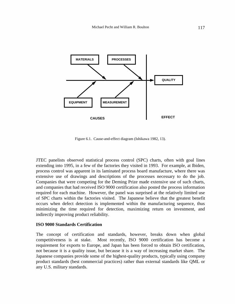
Michael Pecht and William R. Boulton 117
Figure 6.1. Cause-and-effect diagram (Ishikawa 1982, 13).
JTEC panelists observed statistical process control (SPC) charts, often with goal linesextending into 1995, in a few of the factories they visited in 1993. For example, at Ibiden,process control was apparent in its laminated process board manufacture, where there wasextensive use of drawings and descriptions of the processes necessary to do the job.Companies that were competing for the Deming Prize made extensive use of such charts,and companies that had received ISO 9000 certification also posted the process informationrequired for each machine. However, the panel was surprised at the relatively limited useof SPC charts within the factories visited. The Japanese believe that the greatest benefitoccurs when defect detection is implemented within the manufacturing sequence, thusminimizing the time required for detection, maximizing return on investment, andindirectly improving product reliability.
ISO 9000 Standards Certification
The concept of certification and standards, however, breaks down when globalcompetitiveness is at stake. Most recently, ISO 9000 certification has become arequirement for exports to Europe, and Japan has been forced to obtain ISO certification,not because it is a quality issue, but because it is a way of increasing market share. TheJapanese companies provide some of the highest-quality products, typically using companyproduct standards (best commercial practices) rather than external standards like QML orany U.S. military standards.
MATERIALS
MEASUREMENT
PROCESSES
EQUIPMENT
CAUSES
QUALITY
EFFECT

6. Quality Assurance and Reliability in the Japanese Electronics Industry118
The Japan Quality Association (JQA) is responsible for ISO certification. It wasestablished in 1958 as the Japan Management Institute (JMI) under Japan's Ministry ofInternational Trade and Industry for the purpose of export inspection. In 1960, JMI movedfrom inspection to process certification, and in October 1993, JMI was renamed JQA tomore aptly identify its mission. It has provided ISO 9000 certification in Japan since 1990after receiving training from the British Standards Institution's (BSI) quality assurancedivision, and it has memoranda of understanding with both BSI and UnderwritersLaboratory (UL) in the United States for reciprocal certification acceptance.
By October of 1993, JQA had ISO-certified 300 firms in Japan, about 80% of which wereelectronics firms; the rest were chemical firms. JQA expected to have about 540companies certified by the end of 1994. It was already booked through 1994, and therewas a backlog of over a hundred companies waiting for certification. Most firms seekingcertification were electronics firms that depended on exports to Europe. At the time of theJTEC visit, JQA was limited to about thirty assessments per month. It typically tookcompanies one year to eighteen months to gain certification; most had little difficulty inobtaining ISO certification. In addition to JQA certification, there were an equal numberof firms obtaining ISO certification from non-Japanese auditors.
When the JTEC panel visited Japan, Fujitsu, NEC, and Hitachi had the largest number ofcertified factories. Yamagata Fujitsu became ISO 9002-certified in February 1993 and wasapplying for ISO 9001 certification for early 1994. Fujitsu had over ten certified factoriesby the end of 1993. Most of the factories visited by the panel had either received ISOcertification or were in the process of certification.
QUALITY AND RELIABILITY REQUIREMENTS
Quality is associated with the degree of conformance of the product to customerrequirements, and thus, in a sense, with the degree of customer satisfaction. Implicit inJapanese quality products is an acceptable amount of reliability; that is, the productperforms its intended function over its intended life under normal environmental andoperating conditions. Reliability assessments are incorporated through simulation andqualification functions at the design and prototyping stages. With basic reliability designedin, quality control functions are then incorporated into the production line using in-lineprocess controls and reduced human intervention through automation. Since the mid-1980s, Japanese firms have found that automation leads to improved quality inmanufacturing. They have high reliability because they control their manufacturing lines.
Reliability assurance tasks such as qualification are conducted (1) during the productdesign phase using analytical simulation methods and design-for-assembly software, and(2) during development using prototype or pilot hardware. Once again, it is the role ofquality assurance to ensure reliability. Qualification includes activities to ensure that thenominal design and manufacturing specifications meet the reliability targets. In some

Michael Pecht and William R. Boulton 119
cases, such as the Yamagata Fujitsu hard disk drive plant, qualification of themanufacturing processes and of the pilot lots are conducted together.
Quality conformance for qualified products is accomplished through monitoring andcontrol of critical parameters within the acceptable variations already established, perhapsduring qualification. Quality conformance, therefore, helps to increase product yield andconsequently to lower product cost.
Quality Assurance in Electronic Packaging
Japan has a long history of taking lower-yield technology and improving it. In the UnitedStates, companies change technology if yields are considered too low. The continuousimprovement of quad flat packs (QFPs) in contrast to the introduction of ball-grid arrays(BGAs) is an example of this difference. Both countries are concerned with the quality andreliability limits of fine-pitch surface mount products. The Japanese continue to excel atsurface mount technologies (SMT) as they push fine-pitch development to its limits. ManyJapanese companies are now producing QFP with 0.5 mm pitch and expect to introduce0.3 mm pitch packages within the next several years. As long as current QFP technologycan be utilized in the latest product introductions, the cost of manufacturing is kept low andcurrent SMT production lines can be utilized with minimal investment and with predictablequality and reliability results.
Japan's leaders in SMT have introduced equipment for placing very small and fine-pitchdevices, for accurate screen printing, and for soldering. They have developed highlyautomated manufacturing and assembly lines with a high degree of in-line qualityassurance. Thus, in terms of high-volume, rapid-turn-around, low-cost products, it is intheir best interests to push the limits of surface mount devices. Furthermore, QFPs do notrequire new assembly methods and are inspectable, a factor critical to ensuring qualityproducts.
The United States is aggressively pursuing BGA technology; Hitachi, however appears tobe applying an on-demand approach. It has introduced BGA in its recent supercomputerwithout any quality problems and feels comfortable in moving to new technology when itbecomes necessary. Since Hitachi's U.S. customers are demanding BGA for computerapplications, Hitachi plans to provide BGA products. However, Dr. Otsuka of MeiseiUniversity, formerly with Hitachi, believes that for Japanese customers that are still costdriven, QFP packages will reach 0.15 mm pin pitch to be competitive with BGA in high-pin-count, low-cost applications. Dr. Otsuka believes that Japan's ability to continue usingQFP will allow Japan to remain the low-cost electronic packaging leader for the remainderof this decade. Like the United States, Japan is pursuing BGA, but unlike the UnitedStates, Japan is continuing to improve SMT with confidence that it will meet most cost andfunctional requirements through the year 2000. Matsushita and Fujitsu are also developingbumped bare-chip technologies to provide for continued miniaturization demands.
6. Quality Assurance and Reliability in the Japanese Electronics Industry120
Similar differences in technical concerns exist for wire bonding and known good die(KGD) technologies. The U.S. Semiconductor Industry Association's roadmap suggests atechnology capability limit to wire bonding that is not shared by the Japanese componentindustry. The Japanese industry continues to develop new wire materials and attachmenttechniques that push the limits of wire bonding technologies. The Japanese considerconcerns with KGD to be a U.S. problem caused by the lack of known good assembly(KGA); that is, U.S. firms lack the handling and assembly capability to assemble multiple-die packages in an automated, and thus high-quality, manner.
With productivity and cost reduction being the primary manufacturing goals, increasedfactory automation and reduced testing are essential strategies. As TDK officials explainedto the JTEC panelists during their visit, inspection is a critical cost issue:
It is TDK's QA goal to produce only quality products which need no inspection.At TDK, it is our goal to have no inspection at all, either human or machine. Ourlowest labor cost in TDK is 32 yen per minute, or one yen every two seconds. Ifone multilayer semi-capacitor takes roughly one second to produce, then it costsabout 0.6 yen in direct cost. If someone inspects it for two seconds, then we add1.2 yen in inspection cost. That means we have to eliminate inspection to staycompetitive. If we can reduce human and machine inspection, we can improveprofits. Inspection does not add any value to the product.
Quality control is implemented in the manufacturing lines to ensure that the processes staywithin specified tolerances. Monitoring, verification, and assessment of assembly andprocess parameters are integral parts of the manufacturing line. Quality control ensuresthat all process variabilities beyond a specified tolerance are identified and controlled.
The key focus of parameter variability appears to be in manufacturing process parametersand human errors and inadequacies, rather than in materials or parts. Incoming inspectionis negligible because of the view that the quality of suppliers' products can be trusted, andperhaps more importantly because the inspection process is not considered cost-effective.The global move to ISO 9000 certification helps guarantee supplier quality to furtherreduce inspection costs.
Selection of specific quality control methods is dictated by product cost. Hidden costsassociated with scheduling, handling, testing, and production yields become critical withincreasing global competition. As more components are sourced from outside of Japan,these cost factors become increasingly crucial in maintaining competitive costs.
Automation and its impact on quality. The Japanese have determined that manual laborleads to poor-quality output and that automation leads to higher-quality output. Sony’sautomation activities have reduced defect rates from 2000 to 20 parts per million. Qualityhas, therefore, become a key driver for factory automation in Japan. In addition, factoryautomation also adds the benefits of improving productivity and improving flexibility inscheduling the production or changeover of product types. Thus, whenever automation is

Michael Pecht and William R. Boulton 121
cost-effective, it is used to replace manual assembly, handling, testing, and humaninspection activities. This approach is applied to each new product and correspondingproduction line that is installed. For example, the old printed wiring board assembly line atFujitsu’s Yamagata plant used extensive manual inspection, while the new line is in a cleanroom and is totally automated, including final inspection and testing.
All of Nippondenso’s plants have now implemented factory-wide CIM systems. Thesystem at Kota, for example (see Chapter 5), uses factory-level data to meet qualitystandards and delivery times. Boards are inserted into metal enclosures, sealed andmarked, then burned-in and tested before shipping. Out of several hundred thousand unitsproduced each month, only a couple of modules failed testing each month, according toJTEC’s hosts.
Inspection and screening. As noted above, incoming inspection was negligible at most ofthe companies that the JTEC panel visited, because of the view that the quality of suppliers'products could be trusted. Since the 1950s, the Japanese government has set qualityrequirements for any company that exports products from Japan. Suppliers haveprogressed in status from being fully inspected by their customers to being fully accepted.Qualified suppliers are now the standard for Japan, and most problems come from non-Japanese suppliers. Akio Morita of Sony lamented that finding quality U.S. suppliers wasa major challenge for the company. Japanese suppliers were part of the "virtual" company,with strong customer ties and a commitment to help customers succeed.
Components were not being screened at any of the printed wiring board (PWB) assembly,hard disk drive, or product assembly plants visited by the JTEC panel. Defects are seldomfound in well-controlled and highly automated assembly lines. Where specific problemsare found, tailored screens are implemented to address specific failure mechanisms at theboard or product assembly level. For example, Fujitsu noted that today's components donot require burn-in, although at the board level it conducts some burn-in to detect solderbridges that occur during board assembly. But with the increasing cost of Japanese labor,the greatest pressure is to avoid unnecessary testing activities. Suppliers simply have tomeet quality conformance standards to keep customers satisfied. Lack of conformance torequirements would be considered noncompetitive.
With reliable components, assemblers must concentrate their efforts on the assemblyprocess. Within a company's own production lines, automated inspection is central tofactory automation activities. Older lines, like the 3½-inch disk drive line the panel saw atFujitsu, have extensive 100% manual inspection of PWBs. Fujitsu's new line has fullyautomated inspection and testing. At Ibiden, automated inspection is part of the automatedmanufacturing process as a technique for alignment and assembly as well as for toleranceassessment and defect detection. Microscopic mechanical dimensioning is conducted on asample basis. The newer the line, the greater the automation of inspection and testing.

6. Quality Assurance and Reliability in the Japanese Electronics Industry122
Reliability in Electronic Packaging
In terms of reliability, the Japanese proactively develop good design, using simulation andprototype qualification, that is based on advanced materials and packaging technologies.Instead of using military standards, most companies use internal commercial best practices.Most reliability problems are treated as materials or process problems. Reliabilityprediction methods using models such as Mil-Hdbk-217 are not used. Instead, Japanesefirms focus on the "physics of failure" by finding alternative materials or improvedprocesses to eliminate the source of the reliability problem. The factories visited by theJTEC panel are well equipped to address these types of problems.
Assessment methods. Japanese firms identify the areas that need improvement forcompetitive reasons and target those areas for improvement. They don't try to fixeverything; they are very specific. They continuously design products for reduced size andcost and use new technologies only when performance problems arise. As a result, mostknown technologies have predictable reliability characteristics.
Infrastructure. The incorporation of suppliers and customers early in the productdevelopment cycle has given Japanese companies an advantage in rapid development ofcomponents and in effective design of products. This is the Japanese approach toconcurrent engineering and is a standard approach used by the companies the JTEC panelvisited. The utilization of software tools like design for assembly allows for rapid designand is an integral part of the design team's activities. At the time of the panel’s visit,design for disassembly was becoming a requirement for markets such as Germany.Suppliers are expected to make required investments to provide the needed components fornew product designs. Advanced factory automation is included in the design of newfactories.
Training. The Japanese view of training is best exemplified by Nippondenso. Thecompany runs its own two-year college to train production workers. Managers tend to holdfour-year degrees from university engineering programs. Practical training in areas such asequipment design takes place almost entirely within the company. During the first sixyears of employment, engineers each receive 100 hours per year of formal technicaltraining. In the sixth year, about 10% of the engineers are selected for extended educationand receive 200 hours per year of technical training. After ten years about 1% are selectedto become future executives and receive additional education. By this time, employeeshave earned the equivalent of a Ph.D. degree within the company. Management andbusiness training is also provided for technical managers. In nonengineering fields, thefraction that become managers is perhaps 10%.
Ibiden uses "one-minute" and safety training sessions in every manufacturing sector. "One-minute" discussions are held by section leaders and workers using visual aids that areavailable in each section. The subjects are specific to facets of the job like the correct wayto use a tool or details about a specific step in the process. The daily events are intended to

Michael Pecht and William R. Boulton 123
expose workers to additional knowledge and continuous training. As a consequence,workers assure that production criteria are met. Ibiden also employs a quality patrol thatfinds and displays examples of poor quality on large bulletin boards throughout the plant.Exhibits the panel saw included anything from pictures of components or board lots sittingaround in corners, to damaged walls and floors, to ziplock bags full of dust and dirt.
The factory. Japanese factories pay attention to running equipment well, to continuousimprovement, to cost reduction, and to waste elimination. Total preventive maintenance(TPM) is a methodology to ensure that equipment operates at its most efficient level andthat facilities are kept clean so as not to contribute to reliability problems. In fact, theJapan Management Association gives annual TPM awards with prestige similar to theDeming Prize, and receipt of those awards is considered a required step for companies thatwish to attain the Japan Quality Prize. No structured quality or reliability techniques areused — just detailed studies of operations, and automated, smooth-running, efficientproduction.
Safety concerns appeared to the JTEC panel to be secondary to efficiency considerations.While floor markings and signs direct workers to stay away from equipment, few barrierskeep individuals away from equipment. In the newest production lines, sensors are used towarn individuals who penetrate into machine space, and the sensors even stop machines ifindividuals approach too close. Factories provide workers with masks and hats rather thansafety protection like eye wear. In most Japanese factories, street shoes are not allowed.
Most electronic firms the panel visited were in the process of meeting new environmentalguidelines. Fujitsu removed CFCs from its cleaning processes in October 1993. CFCswere replaced by a deionized-water cleaning process. In the old assembly process, theamount of handling required for inspection reduced the impact of cleaning. The new linehad no such problems.
To provide high reliability, Japanese firms create new products using fewer components,more automation, and flexible manufacturing technologies. For example, TDK is strivingfor 24-hour, nonassisted, flexible circuit card manufacturing using state-of-the-art high-density surface mounting techniques and integrated multifunction composite chips. It hasdeveloped true microcircuit miniaturization technologies that integrate 33 active andpassive components on one chip. This will reduce the number of components required bycustomers during board assembly, thereby reducing potential assembly defects.
In addition, the application of materials and process know-how provides a fundamentalcompetitive advantage in manufacturing products with improved quality characteristics.Nitto Denko, for example, has developed low-dust pellets for use in molding compounds.Ibiden has developed an epoxy hardener to enhance peel strength, thus improvingreliability of its plating technology. The new process reduces cracking in the high-stressareas of small vias. Ibiden also uses epoxy dielectric for cost reduction and enhancedthermal conductivity of its MCM-D substrate. At the time of the JTEC visit, the companywas also attempting to reduce solder resist height in an effort to improve the quality and
6. Quality Assurance and Reliability in the Japanese Electronics Industry124
ease of additive board assembly. It believes that a product with a resist 20 mils higher thanthe copper trace can eliminate solder bridging. Sony developed adhesive bondingtechnologies in order to improve the reliability and automation of its optical pickup headassembly. It set the parameters for surface preparation, bonding agents, and processcontrols. Sony used light ray cleaning to improve surface wetability and selected ninedifferent bonding agents for joining various components in the pickup head. It nowproduces some 60% of the world's optical pickup assemblies. The continuous move tominiaturization will keep the pressure on Japanese firms to further develop both theirmaterials and process capabilities.
Quality Improvement Through Comprehensive Waste Reduction
Fundamental improvement means working to eliminate wastes that can negatively affectproduct quality, cost, and delivery time. The Japan Management Association published abook describing the activities of Canon Corporation, Canon Production System: CreativeInvolvement of the Total Workforce, that outlined a number of approaches to improvequality and reliability through "waste reduction" strategies (JMA 1987, 19-22). Theseinclude the elimination of waste associated with defective products, systems planning,work-in-process, human resources, equipment, expenses, and excessive startup time fornew products. Most Japanese electronics firms now incorporate waste reduction as acentral part of their TQM programs.
TQC Management Strategies
The total quality movement in Japan has lead to pervasive top management involvement.Many companies in Japan have extensive documentation on their quality activities. WithKoji Kobayashi, NEC's retired chairman, providing early leadership in Japanese TQCdevelopment, NEC has a comprehensive quality strategy. In 1965, NEC initiated its TQCmovement under the name of zero defects (ZD). In 1972, the NEC Corporation formallyinitiated its total quality strategy, which included the following components:
• quality of management is promoted by all executives
• quality of products and services is promoted within all functional departmentsfrom purchasing and engineering through sales and transportation
• quality of human behavior is promoted within all human resource activities frompersonnel and industrial relations through education and training
• quality of working environment is promoted by all operating and supportoperations concerned with the well-being of the workforce
• quality of community relations is promoted by operational support andenvironmental control divisions
• quality of business operations is promoted by the comptroller's division
• quality of the corporate image is promoted by public relations and advertisingdivisions under the guidance of top management (Satoh 1986)
Michael Pecht and William R. Boulton 125
By the early 1980s, NEC had over 3,000 ZD groups in operation that were generating over43,000 suggestions, and it had received over 14,000 commendations for goal achievement.One of NEC’s major divisions or subsidiaries typically received the Deming Prize each year.
Tadahiro Sekimoto, NEC's current chairman, continues to embrace the TQC philosophy inorder to ensure the continuing survival of today's corporation. He argues that such survivalrequires that companies be thought of as eternal organizations. He was critical of U.S.companies:
In America, the eternal continuity of a company is not always a consideration. If Imay remark in my own words, it seems that in America, companies are continuallysubleased. A company is purchased. It is made over, restructured and thoughpurchased at $10 billion, it is sold for $10.5 billion — this is considered a way ofmanagement. Whether this is proper or not is another question. In Japan,however, most companies, and especially NEC, must be eternal (Sekimoto 1992,220).
Sekimoto further argued that eternal management requires effective management of people— people who have hearts and minds, who must be motivated in the workplace, and who areempowered to accomplish visions of the future. The Deming Prize is simply one method oftesting the organization’s capability to perform at higher and higher levels in the future.
SUMMARY
Japan’s electronics industry has developed its quality management techniques since the1940s, based on the work of American experts like Deming and Juran. Japanese expertshave advanced these concepts into peerless total quality management and continuous wastereduction systems; however, Japanese technology is associated with solving problemsincrementally. There is nothing particularly revolutionary or strategic about their qualityand reliability methodologies. Japanese equipment is very good, very accurate, and verywell maintained. When Japanese firms have a quality or reliability problem, theyinvestigate it thoroughly. They do not investigate areas that are not problems unless that isdemanded by the customer or unless there are competitive issues. Most of the research istargeted at improving next-generation products, components, materials, equipment, orprocesses. It is by dominating in materials, equipment, and manufacturing processes thatJapanese electronics firms have been able to provide the highest quality and reliability intoday's electronics markets.
REFERENCES
Ishikawa, Kaoru. 1982. Guide to Quality Control. Tokyo: Asian Productivity Organization.
Ishikawa, Kaoru. 1985. What Is Total Quality Control? The Japanese Way. Englewood Cliffs,NJ: Prentice-Hall.

6. Quality Assurance and Reliability in the Japanese Electronics Industry126
JMA (Japan Management Association). 1987. Canon Production System: Creative Involvementof the Total Workforce. Stamford, CT: Productivity Press.
Satoh, Yukio. 1986. Challenge to the Quality Revolution. Tokyo: NEC Corporation.
Sekimoto, Tadahiro. 1992. “Perspectives and Directions of Management Strategies in the 1990s,”in Advances in Applied Business Strategy. Vol. 3. Greenwich, CT: JA1 Press.
Tsurumi, Yoshi. 1990. “An Interview with Homer M. Sarasohn: The Unsung American Hero ofJapan’s Total Quality Control System.” In Pacific Basin Quarterly, Winter/Spring: 1-5.
127
CHAPTER 7
SUCCESSFUL PRODUCT REALIZATION STRATEGIES
John PeeplesWilliam R. Boulton
Product realization is the process of defining, designing, developing, and deliveringproducts to the market. While the main thrust of this JTEC panel was to conduct acomplete investigation of the state of Japanese low-cost electronic packaging technologies,it is very difficult to totally separate the development of technology and products from theproduct realization process. Japan’s electronics firms adhere to a product realizationstrategy based on a strong customer focus, a consistent commitment to excellence indesign, and a cost-effective approach to technology commercialization. The Japaneseproduct-pull strategy has been a successful driver and influencing factor in every aspect ofthe product development cycle.
REQUIREMENTS DEFINITION
Defining product requirements is critical to the product realization process. Incomplete orincorrect requirements nearly guarantee a noncompetitive product offering. In a market-driven environment, the establishment of product requirements is clearly a job demanding acustomer focus. The JTEC panel's site visits provided evidence of an extremely tightcoupling between Japanese companies' product realization activities and their targeting ofcustomers' needs. This tight coupling enables the complete and accurate definition of futureproduct requirements. Panelists observed the following examples of Japan's customer focus:
• widely posted customer- and society-based mission statements
• established systems to ensure daily customer contact
• no development programs without identifying a clear customer need
7. Successful Product Realization Strategies128
• early customer involvement, even at the conceptual stage of product design
• standing committees established to solve customer problems
• clearly defined component development strategies that avoid competition withcustomers’ product strategies and simultaneously project future customer requirements
Matsushita's published mission statement provides a clear example of the kind of customerand societal focus found in Japanese electronic firms:
Since its founding in 1918, Matsushita has adhered to the same basic philosophyof product development: contribute to society and improve living standards byproviding products of superior quality and functionality. ...In line with this movetoward creating a more organic, affluent society, Matsushita is entering new fieldsand developing the electronic products that will satisfy customer needs in the 21stcentury.
Japan’s Focus on the Customer
Among the JTEC panel’s most important observations was the tight focus in Japanesecompanies on the market and the customer. No matter what material, component, orproduct companies are developing, they are all trying to meet their customers’ needs.Suppliers are developing material and component technologies that meet the futureminiaturization needs of the end-product companies. Consumer electronics firms aresearching for products that will generate new markets or stimulate existing markets withlower prices or more features. This focus affects all levels of Japan’s electronics industry.Providing lower prices and improved quality requires better designs and manufacturingsystems; improved features require new or improved components and technologies.
Every Japanese electronics firm is looking downstream to meet its customers' future needs;at the same time, many companies are also using their upstream technologies to integrateinto component technologies. Murata, for example, is building on its miniaturizationstrengths in capacitors to develop complete functional radio frequency (RF) modules.Murata is building a gallium-arsenide integrated circuit pilot plant to protect its intellectualproperty and to improve its competitive position in the microwave and RF modulebusiness, with a focus on future personal communication products. By building on its coretechnologies, the company is following the strategy of other electronics firms in findingnew applications or intermediate products whose markets it can dominate. On theconsumer side, Sharp is the most creative firm in finding and using what it calls "senseleaders" to supply product direction. A whole industry of suppliers is ready to supplywhatever electronic packaging technologies and equipment are needed to meet theircustomers’ miniaturization and next-generation product development needs. Suppliersupport and availability of components and equipment reduce development andcommercialization time.
Murata demonstrates one of the strongest commitments to its customers by providing dailycontact with customers. The company so values its customers that it encourages both its
John Peeples, William R. Boulton 129
sales personnel and its application engineers to live within walking distance of keycustomers. The JTEC panel’s hosts at Murata pointed out that accounts are often visitedseveral times daily and/or called as often as six times per day. It would be difficult foranother company to penetrate Murata’s customer accounts without providing equivalentlevels of service and contact. Murata’s people are extremely close to their customers.
Customer involvement in defining product requirements is clearly a part of product planningactivities. At every phase, customers have input. The customer is involved much earlierthan is typical in U.S. firms, participating even at the conceptual phase of the project. Sonyand TDK have both dropped their efforts to develop superconductor technologies due topresent lack of customer interest. TDK, the firm whose founders invented ferrites,canceled its high-temperature superconduction work after realizing that its target customerswould only develop products that operate at normal temperatures. Sony is keeping only aminimal effort in this area for similar reasons. It is important not to confuse thecancellation of work in absence of a customer need with an unwillingness to investstrategically. The JTEC team observed a clear willingness to invest heavily and with greatperseverance in technologies where results were not expected for five or even ten years.For example, Sony's investment in the compact disc took thirteen years to matriculate.Long-term investments occur only when customers’ needs are clearly understood.
The use of problem-solving committees showed the JTEC team a different approach tocustomer support than what some U.S. companies use. Where a team may be formed inthe United States to address and resolve a particular customer problem, several Japanesecompanies reported having specific standing committees devoted to helping customersovercome novel application problems. The intent of these committees seems to be heavilybiased in favor of collecting requirements for future products as opposed to just resolvingcurrent problems. By having such close communications, these companies are able todefine the requirements for next-generation products.
DESIGN FOR EXCELLENCE
A key part of any product realization process is the robustness of the design. In the UnitedStates, many "Design for" initiatives such as Design for Assembly, Design for Cost, Designfor Manufacturing, Design for Test, Design for Logistics, Design for Performance, and soon are now being referred to as Design for Excellence (DFX). The JTEC panel found thatJapanese design emphasizes two key areas: the overall development process and concurrentengineering. As shown in Figure 7.1, there is a strong customer focus at the productplanning phase and in the product evaluation phase of the product development process.The overall product development process is rooted in what Japanese firms call the "market-in." Market-in refers to having a clear set of customer-driven requirements as the basis forproduct development. This is a fundamental requirement for DFX. Concurrentengineering of product design and development activities provides the second main step inachieving DFX.

7. Successful Product Realization Strategies130
Figure 7.1. Japan’s product development activities (Toyoda Machine Tool Co.).
In order to effectively deploy a timely design, thorough testing of the design and processtraining are considered a must. The JTEC panel members toured a number of trainingfacilities affiliated with process development laboratories. Company employees, oftenincluding foreign nationals, receive months of training on specific manufacturing processesbefore equipment is installed overseas.
A successful DFX process requires carefully managed design of new products. As shownin Figure 7.2, there are numerous activities that must be coordinated in order to developand implement a successful product realization effort. Information must be gathered andanalyzed from regions of the globe in which products will be introduced, and productsmust be market-tested in those specific regions. An engine controller for use in anAmerican version of a Japanese automobile, would, by necessity, receive its reliabilitytesting in the United States. Products that are targeted globally, however, also get tested inJapan in order to carefully control the products’ globalization. Technology developmentactivities must operate in parallel with product technology planning and marketdevelopment planning to assure timely development and introduction of new products.
FIGURE 1: PRODUCT DEVELOPMENT ACTIVITES
PRODUCTPLANNING, AND R&D
CUSTOMER PRESIDENT SALESENGINEERING
RESEARCHPRODUCTIONTECHNOLOGY
QUALITYASSURANCE
PRODUCTPLANNING
DESIGNPROTOTYPE,
AND TEST
PRODUCTENGINEERING
PRODUCTIONREPARATION
SALES ANDSERVICE
PRODUCT DEVELOPMENT PLAN
PRODUCT PLAN
PRODUCT/PRODUCTION PROTOTYPING
DESIGN EVALUATION
FACILITIES/PROCUREMENTPLAN
CUSTOMER/CLAIM ANALYSIS

John Peeples, William R. Boulton 131
MARKETREQUIREMENTS
PLAN
TECHNOLOGYIMPROVEMENT
PLAN
INFORMATIONSHARING AND
ANALYSIS
RELIABILITY TESTING
PRODUCT DEVELOPMENTORGANIZATION
PRODUCTTECHNOLOGY
PLANNING
TECHNOLOGYDEVELOPMENT
PLAN
INFORMATIONGATHERING
FUNCTIONALPROTOTYPING
Figure 7.2. Concurrent development requirements (Sony Corp.).
In Japan, product development and market testing is widespread. A visit to the Akibahara,Tokyo's electronics district, introduces the visitor to many consumer products that willnever leave the shores of Japan. The strategy of testing products at home differs from thestrategy of some U.S. companies that test new products in whatever region of the world ismost likely to provide the initial product order. Experience has shown that Japaneseconsumers are more demanding and also more willing to buy new products than consumersin many overseas markets. As a result, the latest versions are typically found in Japan first.The best-received new products sold in Japan are then exported with expectations of highacceptance in overseas markets.
Concurrent Development Activities
Focus on concurrent engineering is prevalent in all the organizations the panel visited. Theprimary objective is to get the overall design right at the lowest cost. This requires makingcritical decisions as to product features/functions, manufacturability, and most importantly,cost. JTEC panelists saw numerous examples of this focus on concurrent engineering inorder to lower product cost. Our hosts at Sony described in detail an effort to develop theadhesives used in the assembly of the CD pickup head in order to achieve cost goals of theproduct line. Similar stories from other companies abound. Functional boundaries aredisregarded once product or cost objectives are specified.
Evidence of Japan's concurrent engineering culture was overwhelming to the JTEC panel.As shown in the following figures, firms use a variety of concurrent engineering

7. Successful Product Realization Strategies132
schematics to depict product, process, and equipment development efforts. For a firm witha core material competence, the product is often a new material, and its schematic wouldshow concurrent development of materials, process, and equipment. Concurrentengineering is a culture in Japan. New products and materials are developedsimultaneously with the processes and equipment needed to produce them.
Japanese firms first attempted to break down functional barriers as part of the TQM (totalquality management) activities initiated to incorporate quality into product designactivities. This was the beginning of what is today referred to as concurrent engineering.The strategic objectives typical of Japanese firms in the mid-1980s were summed up in thequality, cost and delivery (QCD) motto (see Chapter 2). Functional compartmentalizationwas totally inadequate to effectively meet the cross-functional requirements of thesestrategic objectives.
MITI described the first functional integration model based on teams, as shown inFigure 7.3. This approach is a minimum requirement for competitive success in productdevelopment and for facilitating rapid product introductions. MITI points out that closecoordination between functions dramatically cuts time to market. The problem with thismodel is that any one of the functions can still become a bottleneck to developmentactivities because of shared resources. Sharp utilized this model until 1990, when it movedto what is known today as concurrent engineering. A similar problem now faces producersof electronic products that lack manufacturing capabilities in electronic packaging.Without the capabilities to produce and assemble miniaturized components in-house, firmswill be unable to get next-generation products into the market as quickly as theircompetitors.
MARKETINGRESEARCH
BASIC &APPLIED
DEVELOPMENT
PRODUCT DESIGN AND
MANUFACTURING
Figure 7.3. Functional integration required for technological innovations (MITI).

John Peeples, William R. Boulton 133
Going beyond team developments, the concept of concurrent engineering is being practicedin Japan under TQM systems. (Sharp changed the name of its practice from TQM toconcurrent engineering after U.S. visitors in 1990 described what it was doing asconcurrent engineering.) To shorten time to market for new technologies, firms areworking simultaneously to develop component and insertion technologies to be introducedat the time the product is prototyped. As shown in Figure 7.4, concurrent engineeringrequires parallel implementation of all functional activities.
DEVELOPMENT
INDUSTRIAL DESIGN
MANUFACTURING
MARKETING
SALES
SERVICE
CONCEPT CUSTOMER
RESEARCH
Figure 7.4. Concurrent engineering for product innovation (MITI).
In advanced electronics, U.S. product development is going to be limited by the lack ofbasic technologies required for successful production of advanced electronic products.Thorndyke (1993) was not very encouraging to small supercomputer firms in the UnitedStates. He noted that the lack of high-performance packaging technology and assemblycapability was putting them in jeopardy:
The U.S. companies are in danger of being driven out of the market because of thehigh costs of a broad product line and the multi-billion-dollar revenues required tofund the R&D and tooling. The only U.S. companies that can compete in such abroad market [are] IBM, and possibly Cray Research.
The MCC/Sandia report (1993) came to a similar conclusion:
The low cost, high technology manufacturing base of Japan qualifies it to gainsignificant market share in the area of industrial electronics and high performancesystems. To defend existing opportunities and to create new avenues foreconomic growth, North America must develop a similar low cost, hightechnology manufacturing infrastructure. This can only be accomplished througha commitment to manufacturing consumer products, and in particular, consumerelectronics, which can provide the high volume demand necessary to rationalizethe cost of investment.

7. Successful Product Realization Strategies134
Innovation and Improvement
In the area of innovation and improvement, the Japanese focus is on core competencies andon technology. Companies with core competencies in manufacturing and materials includethe following:
Miniaturization and Automation• Sony• Matsushita• Nippondenso
Materials• Ibiden• Nitto Denko• TDK• Murata
The JTEC panel found that the concept of core competencies is well understood by thesecompanies. For example, an excerpt from a Murata annual report reads, "Superiorelectronic materials lead to superior electronic components, which lead to superiorelectronic equipment." The micromachining core competency of Nippondenso is sointegral a part of the company’s strategy that one recent annual report features a 4.8 mmlong micromachined automobile, complete with rolling wheels and license numbers. Aphotograph of the car is printed on a page of a dictionary, positioned on top of the word“creative."
Corporate core competencies enable efficient use of technology; furthermore, processtechnologies enable more rapid product introductions. For example, Ibiden coupled itscompetency in inorganic materials and in electronic laminates (two separate divisions ofIbiden) to develop Ceracom. Ceracom is a low-cost ceramic-cored printed wiring board fordirect chip attach applications that require a substrate thermal coefficient of expansionsimilar to that of silicon. Another example is the surface mount component mountingdensity roadmap that Sony uses to drive its HandyCam development. Sony's TR1 palm-sized HandyCam required the development of a 20 components per square centimeterprocess, nearly double the density of previous models. Sony presents this story as one inwhich the process technology enables the company to achieve its product size objectivesfor next-generation products.
The JTEC panel found that most companies visited have a base technology strategy that isrelentlessly pursued. One panel member had also visited two of the companies in 1990.He said, “In comparing the 1990 and 1993 meetings, I was impressed with the degree oftheir consistency in their technology development activities. I describe this as ‘techno-perseverance’ as opposed to ‘techno-thrashing.’ If you visited U.S. firms on 3-yearintervals, they would most likely be pursuing entirely different technologies in their searchfor ‘silver bullet’ solutions. These Japanese companies covered the identical strategies forfine-pitch SMT development that I had seen in 1990, often using the same identicaloverheads showing progress along the technology timeline. [Chapter 4 covers many ofthese developments.] The point to emphasize here is the tireless pursuit of the technologystrategy and the accompanying resistance to distraction.”
John Peeples, William R. Boulton 135
Increasing Value Added Through Component Development
Successful product realization efforts demand both product and production strategies thatensure adequate gross margins and successful product or product line deployment. Toensure adequate gross margins, companies focus attention on value addition and productphasing. Companies that JTEC visited showed a clear understanding of present costs andvalue added for their products, components, or materials. Consumer electronics productfirms such as Matsushita increase value added opportunities through vertical integration tosupply the value chain for their products. For example, Matsushita provides the substratesand many of the components used in Panasonic VCRs.
For compact disk players' optical pickup heads, Sony developed the design, processes, andequipment necessary to produce them in-house. Today Sony provides 60% of theworldwide market for optical pickup heads for compact disk units. For the 8 mm videocamera, Sony developed the magnetic pickup head and drum and the CCD (charge-coupled device) components as key parts of the overall program. The value added from keycomponents is about 65%, compared to only about 12% for final assembly. Since Sonymakes about half of its key components, it is able to derive 35% value added from in-houseproduction of key components, compared to only 12% for the assembly of 8 mm camcorderproducts. The value added contribution of other products like CD players is similar.
Product phasing into next-generation products is clearly understood in Japan. While U.S.companies seek to extend product life cycles and shorten development cycles, Japanesecompanies seem to more clearly differentiate between product improvements and newproduct introductions. Product improvements occur annually or even semiannually for themost competitive consumer electronic products. New or next-generation products typicallyrequire 1-5 years for development. The Sony Walkman, with 160 model releases since itsintroduction in 1979, has an average model life of less than 18 months. Typically, annualproduct improvements are released in response to competition, and the central labs, inconjunction with factory teams, engage in developing 3rd- and 4th-generation products.
Requirements of Production Skills
The final phase of the product realization process focuses on execution and competition.Keeping product cost low is critical to remaining competitive in the consumer electronicsindustry. The cost objective can be lost for a myriad of reasons. The Japanese concentrateon a set of requirements that include the following: developing what the customer wants;ensuring that the product is manufacturable; targeting and obtaining the desired valueaddition; tuning production processes and equipment for maximum yield (automating toreduce defect rates, to produce miniaturized products, to facilitate rapid offshore start-up,and to free up skilled labor); and utilizing global markets to achieve economies of scale.
The panel found that Japanese firms invest heavily to tune production processes for next-generation products. Each new product generation is designed for the most efficient
7. Successful Product Realization Strategies136
production techniques and equipment. This includes the reduction of the number of partsand the use of standard parts whenever possible. Industrial engineering techniques are usedto optimize velocity and minimize waste in a manual production line. Automation is thenapplied to maximize efficiency and minimize production cost.
Automation has become an essential element of the product realization process at theelectronic packaging level, for several reasons. Increased quality and miniaturization aretwo reasons cited, but Sony automated its Walkman assembly process in order to rapidlydeploy Walkman production to offshore sites. Developing new markets and overcomingcurrency exchange rate barriers are two of Japan's most pressing challenges. Firms arebeing forced to move operations out of Japan to less developed countries in order to staycompetitive. Sony found that its fully automated production line could be deployed andbrought on line in a period of one to three weeks compared to three to six months for amanual assembly line.
Man-machine harmony was also mentioned in most discussions on automation held duringthe JTEC visits. A stated advantage of and reason to automate is to free up human valuefor more complex and creative tasks. Some of this discussion is, in reality, arationalization for the replacement of manpower with automation.
Japanese companies visited by the panel study their competition continuously. Theyrespect and attempt to fully understand their competition at all times, and they appear torelish the “fight.” For example, Konosuke Matsushita wrote in My ManagementPhilosophy, "My proverb about management says that if we fight a hundred wars, weshould win a hundred victories," and also, "You pray for the survival of your rival becauseyou want another chance to demonstrate your superiority."
JAPANESE TECHNOLOGY COMMERCIALIZATION EFFORTS
The following four examples provide unique insights into how Japanese companiessuccessfully bring products to the marketplace.
Murata Manufacturing Company
Murata is a world leader in ceramic capacitors, ceramic filters, and other electroniccomponents. Murata's central technology-driven strategy, shown in Figure 7.5, includesintegrating ceramic materials technology, electronic machinery design technology, andproduction process technology to develop downstream products. Its R&D organization hasbeen set up to carry out this strategy.
Under the corporate-level technical administration division are (1) the fundamentalresearch laboratory for materials, new processes, and HF components, (2) the module andapplication development laboratory for next-generation communications and sensing

John Peeples, William R. Boulton 137
devices, and (3) the machinery and production engineering laboratory for production lineand semiconductor equipment development. Within the product divisions are materials,functional devices, and components laboratories responsible for both product and processdevelopments.
MaterialTechnology
in Ceramics
DesignTechnology
in ElectronicMachinery
ProductionTechnology
and Processes
Productsand
Modules
Figure 7.5. Murata’s integrated technology strategy.
Murata's R&D management approach combines technology roadmaps with technologyprograms targeted at strategic themes. Technology roadmaps identify opportunities forearly involvement in new areas of technology that have long-term potential. To gain aposition in such technologies requires a strategic technology program that will build a corecompetence in the company. The commitment to such technology programs requires along-term vision that fits within the overall direction or business theme for the company.R&D themes require approval by Murata's board of directors in order that appropriateresources can be allocated. Murata currently has 27 strategic technology programs underdevelopment. Each program is reviewed at each phase of its development, starting withsurveys, moving through research, development, application design, and preproduction,and finishing with mass production.
Sony Corporation
Sony has had a balanced strategy for product realization. Its strategy has included thedevelopment of product "sets" that use the company's own components (CCDs), devices(semiconductors), and advanced materials. As demonstrated in Figure 7.6, Sony takesconcurrency to the most comprehensive level to ensure that the entire product componentset offering and infrastructure are being developed in phase. Sony's product-orientedstrategy is coordinated by corporate R&D and includes three critical activities:
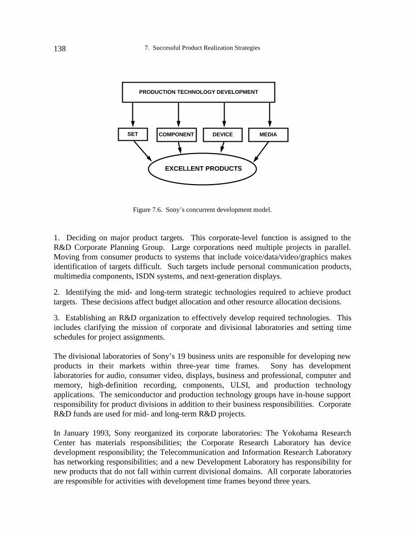
7. Successful Product Realization Strategies138
FIGURE 6: CONCURRENT DEVELOPMENT
DEVICECOMPONENT
PRODUCTION TECHNOLOGY DEVELOPMENT
SET MEDIA
EXCELLENT PRODUCTS
Figure 7.6. Sony’s concurrent development model.
1. Deciding on major product targets. This corporate-level function is assigned to theR&D Corporate Planning Group. Large corporations need multiple projects in parallel.Moving from consumer products to systems that include voice/data/video/graphics makesidentification of targets difficult. Such targets include personal communication products,multimedia components, ISDN systems, and next-generation displays.
2. Identifying the mid- and long-term strategic technologies required to achieve producttargets. These decisions affect budget allocation and other resource allocation decisions.
3. Establishing an R&D organization to effectively develop required technologies. Thisincludes clarifying the mission of corporate and divisional laboratories and setting timeschedules for project assignments.
The divisional laboratories of Sony’s 19 business units are responsible for developing newproducts in their markets within three-year time frames. Sony has developmentlaboratories for audio, consumer video, displays, business and professional, computer andmemory, high-definition recording, components, ULSI, and production technologyapplications. The semiconductor and production technology groups have in-house supportresponsibility for product divisions in addition to their business responsibilities. CorporateR&D funds are used for mid- and long-term R&D projects.
In January 1993, Sony reorganized its corporate laboratories: The Yokohama ResearchCenter has materials responsibilities; the Corporate Research Laboratory has devicedevelopment responsibility; the Telecommunication and Information Research Laboratoryhas networking responsibilities; and a new Development Laboratory has responsibility fornew products that do not fall within current divisional domains. All corporate laboratoriesare responsible for activities with development time frames beyond three years.

John Peeples, William R. Boulton 139
With the continuing recession in Japan, most companies were attempting at the time of theJTEC panel’s visit to improve their R&D efficiencies. Sony was more discriminating inthe selection and weighting of research themes. It was also reevaluating its R&D fundingsystem with a view to reducing corporate funding to 50% of the total and shifting more ofthe funding burden to the business divisions. The company had also established arequirement for laboratories to market their technologies in order to more effectivelydisburse them into the divisions. The corporate development laboratory was set up to helpin technology commercialization, especially for new types of products that were outside thedomain of current business groups. Finally, R&D activities were being centralized withinspecific locations in order to increase the concentration of effort and know-how.
There is no question that Sony is a product-driven company. By focusing R&D activitiesat product targets, it is easier to transfer technologies quickly to the divisions. The criticaltechnologies include materials and semiconductors, key devices like the CCD, andautomation technologies for packaging technologies that are too small for human assembly.Sony Chemical is also working on advanced printed circuit boards (PCBs) and hasdeveloped five-layer boards. Semiconductor developments have a goal of single-chipdeployment in order to reduce package size and increase package density. For example,Sony's 1992 TR1 camcorder achieved packaging densities of 20 components per squarecentimeter, about twice the density of the 1989 TR5 model. The component density targetfor future products is 30 components per square centimeter.
Sony holds monthly meetings between R&D and business groups to share information andresults. There are also general meetings between groups, and two-day internal electronicsfairs are held semiannually. Companies like NEC and Sharp also hold similar exhibitionsin an effort to make divisional personnel aware of potential solutions to their customers’problems and to stimulate new product ideas. Sony has a less structured system than NEC,but at the time of the JTEC visit was considering ways to improve its effectiveness.
Sharp Company
Sharp's market-driven strategy for R&D began by identifying a group of consumers called"sense leaders" to help the company define customers’ needs. Company officials explained
We began to define the market according to the role that people played. Forexample, we consider the most sophisticated people in a market to be theprofessionals. The next level of consumer is the sense leader, then comes thesense follower. At the bottom of the market is the no-sense consumer or the massmarket. Matsushita and Sanyo are after the mass market. Sony and JVC are afterthe professional. Sharp is looking for the sense leaders, those that influence othersto buy new products (Sharp 1993).
From the sense leaders, Sharp began to understand the needs of customers. The videocamera provides one example of Sharp's use of sense leaders. In 1991, video camera sales

7. Successful Product Realization Strategies140
fell 15% to 1.44 million units, far below still camera sales of 4 million units per year. Tounderstand the reason for this decline, Sharp went back to basics:
We took a sample of ten users of video cameras to find out who was buying, howthey were using it, how often they were using it, and for what. From our research,we found two important findings. One major finding was that the time spent usingthis product was very small. For people paying 150,000 to 200,000 yen for thevideo camera, they were only using it thirty hours per year. That was awfully littlefor such an expensive product. Color TVs were viewed 1,200 hours per year,refrigerators throughout a year. Video disc and VTRs, which people didn't usemuch, were used 500 hours per year. Even air conditioners, which are only usedduring the summer, are used 900 hours per year. Thirty hours per year for such anexpensive product seemed awfully small (Sharp 1993).
The research found that the number one usage of the video camera was to tape the firstborn child until kindergarten. That limited the age of purchasers to the latter half of the 20sage group and then only to those who felt obliged to record their child's growth. To expandsales, customer usage had to be changed:
We identified three kinds of pain associated with this product. One is the pain ofhaving to carry it to the destination where you intend to use it. The second is thedifficulty of taking pictures. You are out of the picture and it is difficult to use.The third is the difficulty of seeing the pictures you took. Even if you are tiredwhen you get home, you have to see the pictures. You cannot wait until nextweek. Our conclusion was that we had to reduce these pains and make the videocamera fun to use (Sharp 1993).
Sharp's new concept of the video camera, the ViewCam, incorporated its LCD technology.That required overcoming three technical problems: First was to reduce the weight of thecamera, which became too heavy with the addition of the LCD. Second was to increase thebrightness of the LCD, because it was hard to see the LCD screen in bright light. Thirdwas to reduce the price, because adding the LCD made an already expensive product evenmore expensive. That required overcoming both technology and cost problems. With theproblems identified, a special corporate project was given the challenge of developing thenew product in 18 months. The successful results raised the average use of Sharp'sViewCam to over 300 hours per year, compared to 30 hours for the traditional viewfinder-type camera, and Sharp's market share moved from fourth to second in one year. Sharp’snewest ViewCam can be used as a portable TV display and allows viewing of instantreplays, thereby revolutionizing the camcorder market.
In planning for future product development activities, Sharp's president has encouragedbusiness managers to develop other new products that utilize LCD components. Thecompany's long-term product development will continue to use its competitive advantagein LCD components, as shown in Figure 7.7.

John Peeples, William R. Boulton 141
Photoelectricelements
Polarizedglass
Temperaturesensors
Gas sensors
Sensors
Health
PersonalElectrocardiographs
Digitalthermometers
Blood pressuregauges
Vehicular navigationsystems
Aircraft cockpits
Vehicular Devices
Automotivedashboards
Speedometers
Car radios
Handy dataterminals
Portable dataterminals
POS terminals
MultifunctionaltelephonesCordless
telephones
Communications
OA Devices
Color AX PCs
Facsimiles
Word processors
Pocketcomputers
Laptop PCs
Notebook PCsElectronic
memosElectronic organizers
PA Devices
Personalcomputers
Hand-heldcalculators
with printers
Calculators Solar-poweredcalculators
Electronictranslators
Desktopcalculators
with printers
FA Devices
Measuringdevices
Electronmicroscopes
Elevators
Automaticticket readers
Automaticvending machinesOn-board LCD
AV systems
Pendant clocks
Watches
Talking clocks
Bread makers
Air conditioners
Electronicrice cookers
Refrigerators
Microwaveovens
Vacuum cleaners
Miscellaneous
Clocks
Home Appliances
Pinballmachines
Virtual realitysimulations
3D games
Hand-heldgames
Games
FamilygamesHDTV LCD
projection
Wall-mountTVs
Camcorder
LCD videoprojectors
LCD TVs
CD/radiocassette players
AV Equipment
LCD elements
Illuminationtechnologies
Systemtechnologies
Colorationtechnologies
Unittechnologies
Materialstechnologies
Cell assemblytechnologies
Thin filmfabricationtechnologies
Figure 7.7. Sharp’s expanding LCD applications.

7. Successful Product Realization Strategies142
NEC
Technologically oriented organizations require sophisticated management techniques. Aswith Murata, Sony, and Sharp, superlative management is a key to NEC’s success. NEC's"core technology program," as explained to one JTEC panelist, provides top-down guidanceto tell its people what kind of technology is needed. This is renewed every three to fiveyears by determining what core products will be needed in ten years. Technologies thatwill provide the seeds for growth are also identified. NEC has thirty to forty coretechnologies that are company secrets. Each core technology includes many subordinatetechnologies.
For NEC, success requires that its technologies be effectively utilized in products to meetcustomer needs. For example, NEC has worked since 1965 to develop advanced ceramicstechnologies. In 1970, a low dielectric material allowed NEC to produce small, high-capacitance ceramic capacitors. By the mid-1970s, a semiconductor ceramic material ledto the introduction of ballistors for protecting computers from electric power surges. NECalso introduced new process technology for materials used in packaging, called green sheettechnology. This process was applied in 1980 to make a multilayer substrate used in high-performance and high-speed large computer systems. In 1985, NEC introduced amultilayer ceramic substrate for increasing circuit density by four times. It reduced mediadelay by one-half, for improved computer performance.
NEC's most advanced green sheet technology application was in a high-performance MCM(multichip module) used in its 3900 series large, high-speed computer. The green sheettechnology used polymer, binder, ceramic glass, and powder. The sintered substrate thenused I/O PGA with 11,540 pins and 40 layers. This included the 14 conductive layers; theremainders were used as grounds to reduce noise. The total number of connectionalternatives was the 40 layers times the 11,540 holes per layer (461,600 alternatives, total).NEC had worked on this technology for about fifteen years and finally completed itsdevelopment in 1991. The development of this material and process technology has beenapplied to NEC's fiberoptic interconnect. The new, moderate-priced application allowedNEC to reduce the size of the new component by 70% and reduce the power consumptionby 30%. Future applications will be in NEC's consumer products.
Managing NEC's distributed R&D system requires the matching of market needs withtechnology developments. Contact between central R&D and production R&D isconsidered essential if technology is to be introduced in a timely fashion. Market-orientedbusiness units take the lead in responding to market needs. To facilitate rapid technologycommercialization, NEC uses exhibitions, contract research, and technology strategymeetings. An Exhibition Fair is held yearly to give over 5,000 business unit personnelexposure to NEC's technical capabilities. The exhibitions last for a week and include over2,000 participants. After such exhibitions, R&D personnel contract with the businessgroup to carry out product-related development. At NEC, 30% of the R&D budget is paidfor from such contracts, thereby providing an incentive for cooperation.
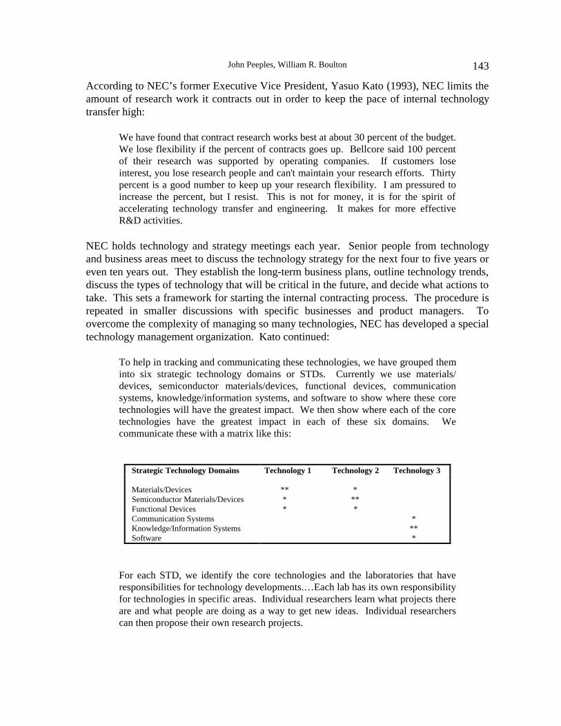
John Peeples, William R. Boulton 143
According to NEC’s former Executive Vice President, Yasuo Kato (1993), NEC limits theamount of research work it contracts out in order to keep the pace of internal technologytransfer high:
We have found that contract research works best at about 30 percent of the budget.We lose flexibility if the percent of contracts goes up. Bellcore said 100 percentof their research was supported by operating companies. If customers loseinterest, you lose research people and can't maintain your research efforts. Thirtypercent is a good number to keep up your research flexibility. I am pressured toincrease the percent, but I resist. This is not for money, it is for the spirit ofaccelerating technology transfer and engineering. It makes for more effectiveR&D activities.
NEC holds technology and strategy meetings each year. Senior people from technologyand business areas meet to discuss the technology strategy for the next four to five years oreven ten years out. They establish the long-term business plans, outline technology trends,discuss the types of technology that will be critical in the future, and decide what actions totake. This sets a framework for starting the internal contracting process. The procedure isrepeated in smaller discussions with specific businesses and product managers. Toovercome the complexity of managing so many technologies, NEC has developed a specialtechnology management organization. Kato continued:
To help in tracking and communicating these technologies, we have grouped theminto six strategic technology domains or STDs. Currently we use materials/devices, semiconductor materials/devices, functional devices, communicationsystems, knowledge/information systems, and software to show where these coretechnologies will have the greatest impact. We then show where each of the coretechnologies have the greatest impact in each of these six domains. Wecommunicate these with a matrix like this:
For each STD, we identify the core technologies and the laboratories that haveresponsibilities for technology developments.…Each lab has its own responsibilityfor technologies in specific areas. Individual researchers learn what projects thereare and what people are doing as a way to get new ideas. Individual researcherscan then propose their own research projects.
Strategic Technology Domains Technology 1 Technology 2 Technology 3
Materials/Devices Semiconductor Materials/Devices Functional Devices Communication Systems Knowledge/Information Systems Software
** * * ** * * * ** *

7. Successful Product Realization Strategies144
NEC's R&D Planning Process. NEC's planning system for technologies is made up of top-down guidelines and bottom-up proposals, as shown in Figure 7.8. Management makes aclear distinction between the setting of policy guidelines and the initiatives of individualsto come up with programs to achieve the company's objectives. These two perspectives arebrought together through joint planning meetings between R&D and operating groups.Yasuo Kato explained:
We have a research proposal system with a history of over 25 years of execution.In October, we have strategy meetings between the top managements of the R&Dgroups and each operating group. During these meetings, each group explainstheir long range plan for their business, makes predictions about their markets, anddiscusses the technologies and R&D requirements that will be needed. R&D willexplain the new technologies and R&D trends and the competition coming fromother companies. At these meetings, group and R&D managers will attempt togain a consensus on what projects are needed, the size of those projects, and theamount of resources needed. An internal contract system is then available so thatproduct groups can contract R&D with the central labs. The average centrallaboratory has 30 percent of its budget paid for by contract R&D. In the C&Clabs, 40 percent of the budget is paid for by contract research (1993).
General Manager
R&D Group
Planning Office
Core TechnologyProgram
Mid-term Plan
R&D Proposal
and
Operation Plan
Laboratories
Meeting on
R&D Strategy
between
R&D Groups
and
Product Groups
Meeting for
Strategic
Discussion
on
Particular
Technology
Figure 7.8. NEC’s technology planning process.
Once the basic strategies have been decided, the implementation begins with actualdevelopment of research contracts between the R&D and operating managers, as shown inFigure 7.9. According to Kato there is a clear framework:
In December, the R&D proposals are made and screened through the end ofDecember. They are read and refined during this time, priorities are set, and theproposals are then linked to the budget. Within this process, we have bothcontinuing project proposals and new project proposals.

John Peeples, William R. Boulton 145
Once projects are determined, contracts are negotiated and signed between the R&Dorganization and the operating groups. Kato further explained:
The internal contract system forces operating groups to be serious about theresearch they want done. It is economical for the operating groups to use thecentral labs. They pay only a part of the R&D costs, but they pay a negotiatedamount. This expenditure gives an operating group stronger motivation for use ofthe research results. The number of them and the amount of requests from theoperating groups are increasing each year.
Lab. Proposals
R&D Planning Office
Laboratories
General Manager
R&D Administration
Headquarters
Total Budget
Check
Fiscal Year Budget
December
January
February
MarchQualifications
Modifications
Presentations
Analysis andEvaluations
R&D Top Managersand Directors
Figure 7.9. NEC’s contract and budget process.
7. Successful Product Realization Strategies146
SUMMARY
Successful product realization in low-cost electronic products in Japan appears to derivefrom a strong corporate focus. Each phase of product realization is supported by criticalactivities that include focusing on the following:
• customer
• process
• concurrent engineering
• core competencies
• technology
• value added
• product phasing
• execution
• the competition
There is no obvious barrier to U.S. companies adopting a similar approach to low-costelectronic product realization. Most of these activities are understood and practiced tosome degree by U.S. companies today. The main challenges come from developing theproper focus and perseverance required for long-term success.
REFERENCES
Kato, Yasuo. 1993. Personal interview with William R. Boulton in Tokyo.
Microelectronics and Computer Technology Corporation and Sandia National Laboratory(MCC/Sandia). 1993. Industrial Competitiveness in the Balance: A Net TechnicalAssessment of North American vs. Offshore Electronics Packaging Technology. (U.S.Department of Energy Contract # AD-3474.)
Sharp Company officials. 1993. Personal interview with William R. Boulton in Tokyo.
Thorndyke, Lloyd M. 1993. “ Supercomputer Packaging Technologies Compared.” SIB, 18 Feb.

147
APPENDICES
APPENDIX A. PROFESSIONAL EXPERIENCE OF PANEL MEMBERS
Michael J. Kelly (Chairman)
Dr. Michael Kelly is Director of the Manufacturing Research Center at Georgia Institute ofTechnology. Prior to accepting that position in October 1991, he was Director of the DefenseManufacturing Office at Defense Advanced Research Projects Agency (DARPA), duringwhich time he was also Executive Director of the National Advisory Committee onSemiconductors. He came to DARPA in January 1989 from the New Jersey Institute ofTechnology, where he was Director of Computer Integrated Manufacturing and TechnologyTransfer.
Dr. Kelly's career includes seventeen years with IBM. His IBM experience included ten yearsin East Fishkill, where he had management responsibilities for designing and developingcomputer-aided design tools, electron beams and related lithography tools, and manufacturingsystem architecture. From 1979 to 1984, he was manager of IBM's ManufacturingTechnology Center in Boca Raton, Florida, with responsibilities for establishing thearchitecture and specifications for computer-integrated manufacturing systems andcontinuing support through implementation at IBM facilities. During that same period, heinitiated the multimillion dollar IBM support of manufacturing-oriented curriculadevelopment at universities and two-year colleges. In 1984, he accepted a special assignmentto assist in preparation for the move of the Corporate Technical Institutes to a new facility inThornwood, New York. During that same year, he became director of the Quality Institute,where he organized the program to educate and train all IBM employees on the principles oftotal quality management. Following his one-year assignment as Director of the QualityInstitute, he transferred to the IBM Systems Technology Division as Manager of QualityImprovement and Professional Development programs, where he worked for theestablishment of quality programs in two IBM plants in the United States (Endicott, N.Y. andAustin, TX) and two IBM plants in Canada (Bromont and Toronto).
Prior to joining IBM, Michael Kelly was an associate professor of electrical and mechanicalengineering and Director of the Engineering Case Program at Stanford University. His otheracademic experience includes three years of teaching at the University of Detroit, where healso served as director of the university's computer center, and four years of teaching andadministration at Marist College. Dr. Kelly holds a B.A. degree from Marist College, B.E.E.and M.E.E. degrees from Catholic University, and a Doctor of Engineering degree from theUniversity of Detroit.
Appendix A. Professional Experience of Panel Members148
William R. Boulton (Editor)
Dr. William Boulton is the Olan Mills Professor of Strategic Management and was theDirector of the Center for International Commerce at Auburn University. He completed hisdoctorate at Harvard Business School in 1977 and taught at the University of Georgia forthirteen years prior to moving to Auburn in 1990.
Dr. Boulton has published extensively on topics related to Japan, competitive strategy, andtechnology management. In an attempt to encourage business schools to teach technologymanagement, he recently completed A Resource Guide on the Management of Innovation andTechnology for the AACBS, the accrediting organization for business schools.
He has lived over six years in Japan since his first visit in 1961. He has worked andconducted research in such firms as Hitachi, Sharp, Matsushita Electric, NEC Corporation,GTE International, and Singer Corporation. In 1986, he was a Fulbright Scholar in Japanresearching the robotics and factory automation industries. In 1991, he was a visiting scholarat the prestigious Institute for Fiscal and Financial Policy, part of Japan's Ministry of Finance.In 1992 he was a visiting professor at Keio University's business school, where he returned inAugust 1993. He continues to research technology management issues in the United Statesand Japan.
John A. Kukowski
John Kukowski currently holds the position of Corporate Fellow at Universal InstrumentsCorporation. Presently he is completing a fellowship at Rochester Institute of Technology,where he is working as a research associate in electronics manufacturing and is enrolled inthe master’s program for computer-integrated manufacturing. Mr. Kukowski is a co-leader ofthe Electronics Industrial Advisory Board and is an active participant in the establishment ofan interdisciplinary electronics design and manufacturing curriculum at RIT.
Mr. Kukowski has been employed with Universal Instruments for 23 years and has served invarious capacities, including tool and die maker, manufacturing engineer, design engineer,Manager of Design Engineering, Manager of Manufacturing Engineering, OperationsManager, Vice President of Engineering, and recently, Vice President of AdvancedTechnology. Mr. Kukowski was the project leader for the first vision-guided placementmachine developed by Universal Instruments and led the implementation of flexiblemanufacturing for the assembly of automated placement machinery.
He holds two patents in automated assembly machine design and has conducted research inthe fields of surface mount assembly of printed circuit boards, tape automated bonding, andflip chip attach. He is a member of the Industrial Advisory Board at Broome CommunityCollege and is the recipient of the Universal Instruments Dale Chubb award for outstandingtechnical contribution.

Appendix A. Professional Experience of Panel Members 149
Eugene S. Meieran
Eugene S. Meieran received his B.S. degree from Purdue University in 1959 and his M.S. andSc.D. degrees from the Massachusetts Institute of Technology in 1961 and 1963, respectively,in the field of material science.
He then joined Fairchild Semiconductor Research and Development Laboratories in PaloAlto, CA, as a member of the technical staff, where he assumed responsibility for thematerials analysis laboratories. In 1973 he joined Intel Corporation in Santa Clara, CA, asManager of Package Development, with responsibility for developing new lines of plasticand hermetic packages for emerging memory and microprocessor products. In 1977 hetransferred to the Quality and Reliability staff, with responsibility for all Intel materials, forthe newly established Analysis and Characterization Laboratory, and for key elements of thewafer fab and assembly reliability functions. For seven years Dr. Meieran was responsiblefor all the quality and reliability functions for the East Asian and Caribbean assembly plants.In 1985 he was appointed Intel Fellow, the second in the company's history. He has beenworking in the fields of statistical process control (SPC) and artificial intelligence in Intel'sManufacturing Systems Technology Group, with responsibility for introducing advancedcomputer and system technologies into Intel's component manufacturing facilities.Dr. Meieran is a member of the Intel Museum Committee, the Intel Research Council, andthe Intel Academic Relations Council. He has received two Intel Achievement Awards forhis contributions to Intel.
Dr. Meieran has taught at Stanford University and the University of California at Berkeleyand has given seminars and invited talks to many universities throughout the world. He haspublished extensively in the fields of SPC, materials analysis, process and product reliability,and more recently, AI applications, with about 50 technical papers published in internationaljournals. He has been awarded three international awards based on technical presentations onhis work in semiconductor device reliability, with emphasis on the phenomena ofelectromigration in thin films, soft error upsets in DRAM devices, and material analysistechnology. Dr. Meieran founded in 1973 and has actively participated in the ElectronicMaterials Symposium.
In 1987, Dr. Meieran was made Distinguished Engineering Alumnus by Purdue University.He has been on the Scientific and Education Advisory Board for Lawrence Berkeley Labsand is currently on the Advisory Board for the Department of ElectricalEngineering/Computer Science at U.C. Berkeley. He was appointed Codirector for the MITLeaders For Manufacturing Program in 1993.
Michael Pecht
Dr. Michael Pecht is a professor at the University of Maryland with a joint appointment insystems research and mechanical engineering. He is also Director of the Computer-AidedLife Cycle Engineering (CALCE) Electronic Packaging Research Center at U.M., which issupported by the National Science Foundation.

Appendix A. Professional Experience of Panel Members150
Dr. Pecht has a B.S. in acoustics, an M.S. in electrical engineering, and a Ph.D. inengineering mechanics from the University of Wisconsin. He is a professional engineer andan IEEE Fellow. He serves on the board of advisors for various companies and was aWestinghouse professor.
He is the chief editor of IEEE Transactions on Reliability, a section editor for the Society ofAutomotive Engineering, and is on the advisory board of IEEE Spectrum. He has edited fivebooks on electronics design, reliability assessment, and qualifications.
John Peeples
Dr. John Peeples is an assistant vice president of manufacturing for AT&T GlobalInformation Solutions (formerly NCR) and Director of the Manufacturing TechnologyResearch Center (MTRC) located in West Columbia, SC. The center identifies, develops orcoordinates the development of and deploys technology to company manufacturing sitesworldwide, with particular emphasis in the area of electronic module assembly and testtechnology. The center is a key concurrent engineering element within the company andowns the corporate design rules for electronic module assembly and test.
Additionally Dr. Peeples is the leader of the Director of Engineering Peer Team for theGeneral Purpose Product Group. This team's mission is to enhance development productivitythrough continuous improvement of the development infrastructure.
Dr. Peeples was with NCR for 17 years prior to becoming part of AT&T management, and hehas served in various capacities within the departments of component engineering, designengineering, management of reliability engineering, product evaluation engineering, andadvanced systems development. He served as director of operations and, prior to his currentjob, as director of engineering for the West Columbia NCR facility.
Dr. Peeples received his B.S. in electrical engineering from the Citadel in 1970 and his M.S.and Ph.D. degrees from the University of South Carolina in 1976 and 1978, respectively.
Dr. Peeples is a member of the IEEE and has served in various capacities, including those ofgeneral chairman and chairman of the board of directors for the IEEE International ReliabilityPhysics Symposium. He is currently the only nonteaching professional on the ScienceFramework Writing Team for the state of South Carolina. Dr. Peeples serves on industrialadvisory boards for the University of South Carolina and Georgia Tech.
Rao R. Tummala
Rao R. Tummala is a chaired professor in the Electrical Engineering Department at GeorgiaTech. Previously, he was an IBM Fellow at IBM East Fishkill Packaging Laboratory inNew York. After joining IBM in 1968, he invented a number of thick film materials andprocesses for IBM's products for magnetic storage, displays, printers, and packaging. In the

Appendix A. Professional Experience of Panel Members 151
process, Dr. Tummala was awarded 21 U.S. patents, made 45 other inventions, published 60papers in professional society journals, and presented over 70 keynote, invited, and othertalks throughout the world. He coedited a book entitled Microelectronics PackagingHandbook, which was recently translated into Japanese.
Dr. Tummala received a B.S. in mathematics, physics, and chemistry, and a B.E. inmetallurgical engineering from universities in India, an M.S. in metallurgical engineeringfrom a Canadian university, and a Ph.D. in ceramics from the University of Illinois.Dr. Tummala is a member of the National Academy of Engineering, a Fellow of theAmerican Ceramic Society, the Technical Vice President of the International Society forHybrid Microelectronics (ISHM), and a member of the Board of Governors of the IEEE-CHMT.
Dr. Tummala received nine IBM Invention Awards, three IBM Divisional Awards, one IBMCorporate Award, and three IBM Publication Awards. He also received the John WagnonTechnical Achievement Award from ISHM, a Best Paper Award from IEEE, the EngineeringMaterials Award from the American Society for Metals, the Distinguished Alumni Award foroutstanding service in engineering from the University of Illinois, and the David SarnoffAward from IEEE.

152
APPENDIX B. PROFESSIONAL EXPERIENCE OF OTHER TEAM MEMBERS
Phillip R. Barela
Mr. Barela works at the Jet Propulsion Laboratory in Pasadena, CA. He began his career atJPL as a failure analyst. Currently he is Technical Group Supervisor for the ApplicationsEngineering Group within Quality Assurance. Mr. Barela is chartered with participating indesign, manufacture, and test of space flight hardware. He actively participates in numerousresearch and development activities that deal with advanced packaging applications for spaceflight hardware. He evaluates packaging designs and develops process controls for low-volume manufacturing with a focus on placing quality assurance in a proactive posture duringdesign and manufacturing.
Mr. Barela worked as an RF electronic systems technician while still an undergraduate. Sincereceiving his B.S. degree in manufacturing engineering, he has filled numerous packagingdesign, failure analyst, and manufacturing positions at Gould Electronics, NavCom DefenseSystems, Loral Electro-Optical Systems and the Jet Propulsion Laboratory. Mr. Barela hasserved as lead manufacturing engineer in hybrid (thick and thin) MCMs, COB, through-hole,surface mount, and mixed assembly facilities. In this capacity, Mr. Barela started numerousproduct lines for low- to medium-volume military and space products. He has extensiveexperience with producibility issues relating to new and mature product lines (e.g., DOE,QFD, DFM, DFI, DFR, SPC, etc.).
Mr. Barela is a certified manufacturing technologist through the Society of ManufacturingEngineers (SME). He is a member of SME, ISHM, SMTA, SOCE, EOS/ESD Assoc. and theIPC. Mr. Barela is currently attending UCLA, working towards his master's degree inmanufacturing engineering.
George Harman
George Harman is a Fellow at the National Institute of Standards and Technology (formerlyNBS), Chair of the IEEE CHMT's Fellows Committee since 1988, and President of ISHM(1994-1995). He was a Trustee of the Federation of Materials Societies (1988-1990) as wellas the Chair of the IEEE CHMT society's nominating committee (1982-1988). Mr. Harmanis a Fellow of the IEEE and ISHM, Member of IEPS, American Physical Society, ASTM,Sigma Xi, and Sigma Pi Sigma.
Since 1984, Mr. Harman has traveled to East Asia (Singapore, Malaysia, Taiwan,Hong Kong, Philippines, Korea, and Japan) lecturing and consulting at 17 American-ownedfacilities.

Appendix B. Professional Experience of Other Team Members153
Mr. Harman has received numerous awards. The Department of Commerce awarded him theSilver Medal (1973) and the Gold Medal (1979). NIST awarded him the E.U. CondonAward for best publication in 1990. He received the Centennial Medal (1984), CHMTOutstanding Contributions Award (1992), and the ECTC Sustained Distinguished ServiceAward (1993) from IEEE. ISHM has also conferred several awards on Mr. Harman,including its Technical Achievement Award (1981), Lewis F. Miller Award (1984), DanielC. Hughes Award the society's top award, (1988), and the ISHM Foundation DistinguishedService Award (1990).
Mr. Harman received a B.S. in physics from VPI & SU, and an M.S. in physics from theUniversity of Maryland. He was a Research Fellow at the University of Reading (England).He has published 40 papers, one book (a second is under contract), and has been granted 4patents.
M. Gene Lim
M. Gene Lim is President of SEAM International Associates and a member of the IndustryAdvisory Board for the Rochester Institute of Technology. He is a consultant for the Institutefor Defense Analyses (IDA) and Systems Planning Corporation (SPC) for the U.S.Department of Defense. Dr. Lim previously was President of Westinghouse Nuclear, Korea,in Seoul, Korea. Prior to that he was Manager of Japan Operations for Westinghouse inKobe, Japan.
Gene Lim has 17 years of overseas-based experience in government affairs, technologytransfer and license administration, marketing, and project implementation for internationalprojects in Japan and Korea. Dr. Lim received his Ph.D. in nuclear science and engineeringfrom the University of Virginia.
Nicholas J. Naclerio
Nicholas J. Naclerio is a program manager in the Electronic Systems Technology Office ofthe Advanced Research Projects Agency (ARPA). In that capacity, he manages several majorelectronics manufacturing initiatives including SEMATECH and ASEM. ASEM is a newARPA program aimed at developing a merchant supplier infrastructure for application-specific electronic modules. He also serves as executive director of two federal advisorycommittees: the National Advisory Committee on Semiconductors (NACS) and the AdvisoryCouncil on Federal Participation in SEMATECH. Prior to joining ARPA he held positions atthe Air Force's Wright Laboratories as Chief of the Manufacturing Technology Directorate'sInformation Management Branch and earlier as a research program manager in the DesignBranch of the Electronic Technology Laboratory.
Appendix B. Professional Experience of Other Team Members154
Dr. Naclerio holds a bachelor's degree in electrical engineering and computer science fromDuke University, a master's degree in material science from the University of Cambridge(England), and a Ph.D. in electrical engineering from the University of Maryland. He haspublished numerous articles in areas such as microcircuit fabrication, computer-aided designalgorithms, and engineering information systems.
Linton G. Salmon
Dr. Salmon recently completed a tour as the director of the solid state and microstructuresprogram for the National Science Foundation. In that capacity, he directed NSF funding ofresearch in electronic materials, semiconductor manufacturing, advanced processes,electronic packaging, and microelectromechanical systems (MEMS). Dr. Salmon came toNSF from Brigham Young University, where he has now returned to his position asAssociate Professor. His current research interests include MEMS applications andpackaging, multichip module packaging, and high-speed VLSI integrated circuits. Previously,he was Director of GaAs Engineering at Rockwell International, where he directed thedevelopment of advanced designs and processes for III-V integrated circuits and multichippackaging. Earlier he was head of GaAs Technology and Molecular Beam Epitaxy Sectionsat Hughes Research Laboratories. He received his B.S. degree in Physics from StanfordUniversity, M.S. and Ph.D. degrees in Applied Physics from Cornell University.
R. Duane Shelton
Robert Duane Shelton has led international technology assessments since 1984, as sciencepolicy analyst at NSF, and now as ITRI Director. He is currently on sabbatical from LoyolaCollege in Maryland , serving as IEEE Congressional Fellow in the office of Rep. LloydDoggett (D. TX).
Dr. Shelton's degrees are in electrical engineering from Texas Tech (MCL), MIT (as NSFFellow), and the University of Houston. Dr. Shelton worked at Texas Instruments onelectronics R&D and at NASA in performance analysis of the Apollo space communicationssystem and of TDRSS — the system currently used for Shuttle communications.
He has been a professor at the University of Houston, University of Louisville, Texas TechUniversity, and now Loyola College. During this time, he has served as principal investigatoron 35 grants, has written 58 technical papers and one book, and has chaired 57 M.S. and 3Ph.D. thesis committees. He has chaired academic departments of applied mathematics,computer science, and electrical engineering. His current research interest is science policyanalysis: international technology assessment, high-technology trade problems with Japan,and national strategies for engineering education.

155
APPENDIX C. SITE REPORTS
Site: Fujitsu (Yamagata Plant)1-6-1 Marunouchi, Chiyoda-Ku,Tokyo 100, Japan
Date Visited: October 6, 1993
Report Author: M. Pecht
ATTENDEES
JTEC:
P. BarelaW. BoultonG. HarmanG. MeieranM. Pecht
HOSTS:
C. Handa President, Yamagata FujitsuT. Tsuchimoto Board Director, General Manager of Technology
Group, Kawasaki FacilityM. Nakazono Director and General Manager, Yamagata Fujitsu
BACKGROUND
Fujitsu manufactures and automates to the level needed to reduce costs and improve qualityincrementally; nothing more, nothing less.
Our JTEC group spent a half day at Yamagata Fujitsu (Fujitsu’s Yamagata plant). The maintechnology that we came to see was Fujitsu’s high-volume surface mount operations that arepart of its manufacturing process for hard disk drives used in PCs and workstations. We weregreeted by Chiaki Handa, President of the Yamagata plant, and by T. Tsuchimoto, BoardDirector and General Manager of the Technology Group at the Kawasaki Facility, who gave ageneral overview of the operations of Fujitsu. Then M. Nakazono, Director and GeneralManager of the Yamagata plant, gave the Yamagata plant overview. Altogether there were12 managers from three different Fujitsu facilities (Yamagata, Kawasaki, and Atsugi).
Fujitsu has some 71 overseas manufacturing and assembly-and-repair subsidiaries, inaddition to numerous sales and other offices. It currently lists 161,974 employees worldwide.
Appendix C. Site Reports156
(This number does not include employees from Amdahl and other similar affiliates inEurope.) In addition to manufacturing computers, Fujitsu has entered the multimedia marketand has been chosen by U.S. common carriers for broadband ISDN equipment, switchingsystems, optical transmission systems, and cellular mobile phones; it is offering similarequipment in parts of Asia, Australia, and Europe. It is also moving into software and othercomputer services around the world.
YAMAGATA FUJITSU
Yamagata Fujitsu is located in Japan’s industrial district. Established in 1983, it had 100%investment by Fujitsu; 70% of sales go overseas. As of the JTEC visit, approximately 300 of1,000 employees were staff, approximately 700 were operators; about 60% were male and40% female; their average age was 24. The plant developed, produced, and managed sales ofdisk drives. The JTEC group toured the printed circuit board (PCB) assembly line (PCA) for3-1/2 inch disk drives and the 2-1/2 inch hard disk drive assembly line (HDA).
Printed Circuit Assembly Line for 3-1/2 Inch Disk Drives
Yamagata Fujitsu’s PCA line incorporates traditional semiautomatic component placement,soldering, and cleaning equipment with manual part and assembly feeding of machines.There was some manual part soldering and a lot of manual inspection, testing, and repair. Thereasons given for all the manual work were (1) it was the most cost-effective considering themix of PCA technologies they needed to handle, (2) there were many odd parts, such asspecial connectors and heat sinks that didn't easily lend themselves to automation, and (3)product demand was low, so that only two shifts were needed and further automation wouldnot pay off. Over 600 pieces per minute could be manufactured. The components werepredominantly plastic. Generally 60% of the boards were composed of SMT; 20% of thesewere single-sided and double-sided boards, 45% were four-layer, 30% were six-layer, and 5%were eight layers and up. In general the PCA process line was not by any meansstate-of-the-art and may not even be highly profitable. It was stated that the demand for theseproducts was down.
The 3-1/2 inch drive had a lot of manual handling: for insertion of some components, forrework, and for inspection. Burn-in equipment at the plant operates under the followingconditions:
• There are some fans covered with stainless steel mesh at the bottom of this equipment tocirculate the inside air.
• There are no heaters inside the equipment. As a number of hard disk drives are operatingwithin a closed box, temperature inside the box increases significantly because of heatradiation from the disk drives. As a consequence, all hard drives kept in the box areburned-in under this high temperature even with no heaters.

Appendix C. Site Reports 157
• In case of a perfectly sealed system, temperature becomes too high, so, a slit is put on thetop side to maintain the hard disk drive's temperature at a range between 67oC and 73oC.The location and size of this slit are based on Fujitsu's know-how.
The cleaning operation was OK, but there was so much handling after the cleaning with barehands that it seemed as if the cleaning was somewhat superfluous. Of some special interestin the PCA manufacturing line was the removal of CFCs in October 1993 and the subsequentuse of non-CFCs, replaced by a deionized water cleaning process. While there was noresearch being conducted in leadless solder, management was aware of efforts in Germanyand did look at InSn, but considered it too expensive.
The small FR-4 boards (to be mounted in hard drives) were demarked and partially cut outbut remained in the larger mother boards for handling. Each mother board contained four orsix smaller active boards. They were loaded with pick-and-place machines (said to have aplacement accuracy of 50 µm — at other sites we saw machines that were more accurate, but50 µm was apparently adequate for the purpose). The boards were reflow soldered.
In summary, the printed circuit line for 3-1/2 inch discs was "low tech": the machinery wasold; the process was a combination of automated and manual assembly; there was lots ofinspection; cleanliness was minimal; the burn-in was primitive. It was clear, however, thatthe important processes were well developed, and all the things we saw that seemed "low-tech" were indeed relatively unimportant (e.g., the burn-in caught what it needed to catch, andhaving a more sophisticated burn-in system was unnecessary, and hence no attention waspaid to it). Thus, the operation appeared efficient for what it was doing, even though it wasnot elegant. It was obvious that Fujitsu has no intention of significantly improving this line.It was also obvious that Fujitsu was going to use what it learned on this line to make astep-wise improvement on its 2-1/2 inch drive assembly.
It should be noted that the Yamagata plant is dedicated to manufacturing products forpersonal use, different from any other Fujitsu plant, such as its Numazu plant, whichmanufactures high-technology products. The main focus of the Yamagata plant is to utilizethe existing equipment to a maximum extent to promptly manufacture high-quality productsand at the same time to seek better production efficiency at a lower cost.
As pointed out to the JTEC team, the Yamagata plant uses traditional manufacturing methodsthrough semiautomated equipment and manual work on its printed circuit board assemblylines. While installed machines at the Yamagata plant such as screen-printer, parts-mounter,and air-reflow oven may be obsolete from the technical point of view and give the impressionthat the Yamagata plant continues to use old equipment, our hosts noted that the use of thisequipment is optimal from the point of view of efficient investment.
The plant does utilize an automatic appearance inspection tester for any minimum-size partssuch as QFP (quad flat package) with 0.5 lead-pitch and 1005 chips, which are almostimpossible to inspect manually. On the other hand, inspection and repair of any parts other

Appendix C. Site Reports158
than those minimum-size ones are carried out by manual tasks to maintain efficiency incapital investment.
Hard Disk Assembly Line
The hard disk drive assembly (HDA) line was highly automated and the equipment wasmodern and sophisticated. The environment was a 100-class clean room (not great bysemiconductor standards, but certainly sufficient for the operation, especially since extraprecautions were taken on the equipment where the magnetic heads were physically present),with automated testing of over 100 drives simultaneously. There was complete robotichandling of parts. The operators all wore appropriate clean-room clothing. This line wasbeing prepared for high-volume production. The hard disk assembly operation was a modelof efficiency. The entire operation was automated using Fujitsu-built robots and requiredattention to technology and detail. The striking difference between the PC board assemblyarea and the hard disk area was attributed (by us) to the fact that the disk was the guts, thefamily jewels, of the Fujitsu system; hence, no expense was spared to make this as efficientand low-cost as possible.
New Technology
We saw very little in terms of new technologies, but our hosts did mention various technicalactivities in other parts of Fujitsu, including 16-to-42-layer PC boards, 60-layer ceramiclaminates used in its supercomputers, and the newest parallel supercomputer using GaAschips. (These are mounted in single-chip packages that are then mounted on ceramic boardsin order to get around the known-good-die problem.) Fujitsu was using opto-connections forexternal connections but using electrical connections inside. It developed its own router forthese boards.
Our hosts also mentioned a new (but published in MRS in 1992) photosensitive dielectricfilm using a blend of polymers that can be used for cheap MCM-D circuit boards. Linewidths were 30 µm, and vias were claimed to be about 20 µm in diameter. They used Almetal lines and made up to four metal and four dielectric layers. They said this might be inproduction within two to three years.
Our hosts said they were following the work in BGAs including the OMPAC by Motorolaand some products by AMD. They were conducting some work in flexible PCBmanufacturing and assembly, flip chip mounting and TAB mounting, with plans for bare chipassembly on a computer product (server) in 1994.
Quality and Reliability
Quality and reliability were assumed, but never initiated as a topic of discussion by our hosts.Their policy is summed up as "quality built-in," with cost and performance as prime

Appendix C. Site Reports 159
considerations. Our hosts noted that today's components do not require burn-in, although atthe board level there was some concern for solder bridges.
In February 1993 Yamagata Fujitsu became ISO 9002-certified and at the time of our visitwas expecting to be 9001-certified later in 1993 — the purpose is to be able to sell productsin Europe.
Management Philosophy
As in other Japanese factories the Yamagata plant management paid attention to runningequipment well, to continuous improvement, to cost reduction, and to size reduction. Nomagic technology was employed; just fruits of a detailed study and execution of automatedprocessing and smooth-running, efficient operations.
SUMMARY
Fujitsu is motivated to improve circuit board density and reduce cost. The improvement indensity had several implications; for example, to reduce package thickness, to improvemounting location, and to reduce weight. Reducing cost was the prime driver afterfunctionality and customer needs were accounted for.
To meet the objectives, Fujitsu was going to use flexible printed circuits, improved solderingtechnology, design of thinner packages, and specially plated through-holes. None of thetechnologies are revolutionary; rather, they are the straightforward application of continuousimprovement to Fujitsu product lines.
A Fujitsu representative aptly stated, "Indeed, we are still using an old-type equipment for theprinted circuit board assembly line for 3.5 inch disk drives. We would like to stress,however, that the use of the fully automated equipment does not always represent ‘hightechnology.’ Through our experience over years, we have come to the conclusion that incertain cases manual work is sometimes more efficient rather than automated machines, asother vendors do in some cases."
Appendix C. Site Reports160
Site: Hitachi PERL and HIMEL292 Yoshida-cho, Totsuka-kuYokohama-shiKanegawa-ken 244, Japan
Date Visited: October 6, 1993
Report Author: L. Salmon
ATTENDEES
JTEC:
P. BarelaJ. KukowskiL. SalmonR. Tummala
HOSTS:
Dr. Hiroyoshi MatsumuraMr. Ikuo KawaguchiMr. Toshiro KinugasaMr. Ryugi NishimuraMr. Masahiko YatsuDr. Norikazu TsumitaDr. Toshio AsanoMr. Takanori NinomiyaDr. Hisashi SugiyamaDr. Makoto Iida
BACKGROUND
Hitachi has nine corporate research laboratories with approximately 5,700 employees. Thecorporation spends approximately $3 billion per year on research and development. Thisamount corresponds to approximately 10.5% of total sales for the company. The firstcorporate R&D laboratory, the Central Research Laboratory, was established in 1952. Wevisited two of the corporate research laboratories, the Production Engineering ResearchLaboratory (PERL) and the Hitachi Image and Media Systems Laboratory (HIMEL), whichare both situated at the Yokohama site together with the Systems Development Laboratory.
PERL is a corporate research laboratory and has as its major goal research in the areas ofadvanced packaging, precision machining, factory automation, high-density magnetic media,

Appendix C. Site Reports 161
and advanced semiconductor materials and processing. The laboratory has approximately600 employees and was established in 1971.
HIMEL is also a corporate research laboratory and is chartered to perform research intechnology areas of importance to camcorders and other optical consumer products. Thelaboratory has approximately 400 employees and was established in 1972. The laboratorywas originally an associated division of the Consumer Products Group, but was designated asa separate research laboratory in February of 1993. Its purpose is to work closely with theproduction divisions to provide technology required for new products. HIMEL is divided byproducts into four departments: projection displays, range finder video cameras, LSI designand fine mechanism development, and fax/word processors.
Hitachi's philosophy regarding research is called Tokken and is based on tight couplingbetween production and R&D efforts. Connections between production and R&D groupsinclude personnel exchange, common planning, and frequent meetings to assure coordination.The charter of each of the organizations in Hitachi is summarized in Table PERL.1. Thischart is idealized and is not always rigidly followed. Research staff will sometimes work atthe development facility for extended periods during technology transfer. In other cases, thedevelopment staff may come work at the research facility for an extended period.
Table PERL.1Summary of Organizational Responsibilities
CentralResearch
ProductionResearch
Development Production
2nd Generation Next Generation Prototype Current Product
Mr. Kinugasa from HIMEL first gave a presentation on Hitachi’s design and manufacture ofcamcorders. He began with presentation of a roadmap for reduction in camcorder sizethrough integration of camcorder functions into fewer LSI and fewer discrete components.The path he outlined shows an evolutionary approach to reducing the number of componentsand does not hope for revolutionary changes in IC technology for at least the next four years.He projected continued use of hybrid and PCB technology to package the components andexploitation of shrinking feature sizes in IC technology. TAB and bare chip technology arenot part of the current packaging plan because these technologies are more expensive toproduce. Current PCBs are designed with a 0.5 mm pitch. Efforts are under way to decreasepitch size to 0.4 mm and 0.3 mm, and the technologies will be included in products if the costis not too high. Hitachi is developing optical inspection techniques for 0.3 mm technologybecause x-ray inspection is blocked by the large number of metal layers on the PCB.Inspection for 0.3 mm is currently performed manually. The most advanced SMT process
Appendix C. Site Reports162
Hitachi has developed is 0.3 mm pitch on a six-layer PCB that is 1.6 mm thick. The solderpaste screen is made using an Ni additive process. Super solder is not used because solderdeposition was found to be too uneven.
Mr. Kinugasa indicated that packaging accounts for 20% of IC production cost, and heanticipates that the percentage cost will continue for new products. The major impediment todramatic reduction in camcorder size is the size of the recording tape and associatedmechanical parts required to read and write to the media. During a tour of HIMEL facilities,our hosts indicated that HIMEL is seeking to reduce discrete component size below the 1005size part. They also indicated that the plan for HIMEL includes development of thetechnology required to build a pocket-size, all-solid-state camcorder. Our hosts suggestedthat some effort is being expended to investigate bare chip technology using conductiveadhesives in order to address environmental concerns regarding lead-based solders.
The JTEC team was given a tour of the clean-room facility used to pursue research in theareas of advanced disk drive media and thin film MCM development. The facility isapproximately 10,000 ft2 and is class 100/1,000. PERL is also investigating high-densitymagnetic media and advanced thin diamond-like coatings to protect hard disk media.Research on magnetoresistive magnetic storage is carried out at a separate Hitachi laboratory.
The thin-film-on-ceramic MCM process is being pursued to support high-performancesupercomputer applications. The technology provides excellent thermal properties and isdesigned to dissipate heat from high-power ICs. Dr. Inoue indicated that the technology willbe used for the next generation of high-end supercomputer, but that it is unclear whattechnology will be used for packaging for the generation after that. He stated that thin-filmMCM technology may be important for workstations, but that the cost of the process willhave to be decreased significantly before the technology can be used in that area. Currentresearch efforts are concentrating on cost reduction in the process, but there are no immediateplans to use the technology in Hitachi workstations. We were told that this technology wouldnot be used for consumer applications due to its high cost.
We were given a tour of the facilities for several projects at PERL. There is a strong effort todevelop the technology and equipment required to automatically inspect and evaluate thequality of products and processes. Successful equipment and techniques developed in thelaboratory are immediately implemented in the manufacturing line. PERL makes extensiveuse of image processing to decrease highly accurate inspection of high-definition CRTscreens. PERL is also active in developing systems to automatically inspect green sheets formultilayer ceramic packaging and solder quality in SMT reflow processes.
Scientists at PERL have developed an advanced PCB that they call TAF-II. The process usesan additive metalization process that results in improved resolution: line widths as small as140 microns in 35-micron-thick copper. The process flow for the TAF-II process is shown inFigure PERL.1. The lamination, drilling, and catalyzation steps are similar to those instandard PCB processes, but the following steps differ from standard processes: Solder resist

Appendix C. Site Reports 163
is formed through an etched stencil; the plating process is an electroless plating step in a bathwith a pH of 12. The PCB typically contains 4-6 layers, but the PERL researcher claimedthat the process would support as many as 12 layers. He also claimed that the TAF-II processis 20% less expensive than the standard PCB process because less plating solution is used inthe selective plating process. The TAF-II process was licensed to several companies in 1989,and a new process, TAF-III is in development. TAF-III will use lithography to define thesolder resist layer and will have line widths as small as 80 microns.
Figure PERL.1. Brief process flow.
Dr. Makoto Iida presented work on thin molded plastics for laptop computer cases. Heshowed research on methods to reduce the thickness and mass of the plastic required for adomestic Japanese portable PC product, describing a roadmap for thinning body plasticthickness from 3 mm in 1985 to 1.5 mm in 1993. PERL researchers are currently working toreduce the size of the plastic case by improving structural design of the case, the polymermaterial used in the case, and mold design. Hitachi has developed its own polymericmaterial, together with an associated company. One of the greatest challenges is to controlflow of the resin during filling of the mold. PERL researchers have analyzed resin flow using

Appendix C. Site Reports164
a simulation program to predict the best method to inject resin into thin molds. Dr. Iidastated that although composite materials can be made thinner, they are only used in higher-value products such as computer pen pads, due to the high cost of the material. Compositematerials can be molded as thin as 1 mm and weigh less than conventional plastics. Overallthickness of the portable product was also reduced by using the LCD display as a structuralmember. A shock-absorbing material was used to assure that LCD reliability remained high.Dr. Iida indicated that PERL is investigating molded circuit boards, but present cost ofmaterials is very high. He indicated that the thermal expansion characteristics of the moldedcircuit board material are very important.
Dr. Iida then described a rework tool that has been developed to add or remove solder fromSMT parts with a pitch as small as 0.3 mm. The tool removes excess solder using a braidedwick, and adds solder using a novel technique. A droplet of solder is held by surface tensionto the end of a heated point and the solder is placed on the unsoldered joint. The solder andthe lead are heated in a single step.
There were several general comments made during the JTEC visit to Hitachi that are worthyof note. First, although a high level of automation is evident in the production philosophy ofHitachi, individuals at PERL emphasized the importance of an “appropriate” level ofautomation. They stressed that overdependence on automation is as detrimental asunderdependence on automation. They further stressed the importance of the skilledindividual to improve production yield and to retain production flexibility. The managers atPERL indicated that process floor workers should have a college education. When asked,they agreed that it is difficult to attract high-caliber people to production tasks, but indicatedthat showing employees the importance of their contribution to production is the best methodto attract them.
A second theme was the importance of cost in all decisions regarding technology. Cost wasclearly a critical consideration in every discussion regarding proposed technology. There wasalways a clear product path, and the cost of a technology was compared to a projected,required production cost. One statement made by Dr. Matsumura summarized this attitude. He said, “We used to determine the price of a product by adding an acceptable profit marginto the projected cost to produce a product. Now the price is a predetermined quantity, and weadd an acceptable profit margin to arrive at the required product cost.”

Appendix C. Site Reports 165
Site: Ibiden Co., Ltd.3-200, Gama-Cho, Ogaki CityGifu Prefecture 503, Japan
Date Visited: October 5, 1993
Report Author: J. Peeples
ATTENDEES
JTEC:
M. KellyG. LimN. NaclerioJ. Peeples
HOSTS:
Mr. Hidetoshi Yamauchi Corporate Overseas Planning OfficeMr. Kazuhisa Ohno Manager of Sales and Marketing for the
Overseas Affairs DivisionMr. Osamu Fujikawa Director of Technology and DevelopmentMr. Koji Hosada General Manager of Overseas Marketing and
Sales of ElectronicsMr. Keiji Adachi Sales Engineer, Overseas Marketing and Sales
of Electronics
BACKGROUND
Ibiden began life as a power company and is now a manufacturer as well. It offers productsin the following three areas:
IBI Electronics Branch
• double-sided/multilayer/special boards (small)• IC packaging based on the special board technology• continuous processing• up to 12 layers • width traces in the lab• small vias and blind/buried vias• flip chip on board (COB) for one customer• aluminum core substrates for power dissipation

Appendix C. Site Reports166
IBI Inorganic Chemical Branch
• calcium carbide/carbon/acetylene for the steel industry• fine-grain graphites - electrodes/fixtures• ceramic fibers - IBI, wool, insulator IBI Building Materials Branch
• IBI board - laminate material for home construction and decor• nonflammable construction materials
Ibiden shares its product branches between manufacturing plants. Any given plant may beinvolved in the production of electronics, building materials, inorganic chemicals, and/or newproducts. Generally, however, one or two plants specialize in production for a particular branch.
R & D ACTIVITIES IBI-Techno is the calling card of Ibiden's R&D activities. Advanced product development isconducted in the New Products Development Branch. When ready, the technology is fusedinto one of the major product branches. The development of plastic pin grid arrays (PGAs)and application-specific integrated modules (ASIMs) were discussed as examples of thisadvanced product development process. Ibiden discussed the ASIM concept with me duringmy April 1990 visit. I could not detect that the concept was any closer to product at the timeof the JTEC visit in late 1993. Fundamental technology development is the charter of the Technology and DevelopmentDepartment. Activity in this area includes investigation of biotechnology, superconduction,ceramats, and optical materials.
Ibiden Electronics is working mainly in two product areas: IC packages and printed wiringboards (PWBs).
IC Package Products
Ibiden has leveraged its competency in laminate substrates technology into an IC packagebusiness. It makes small interposer substrates with facilities for chip attach (plated wirebondpads, semi-cavities, etc.) and add pins. Its major product line, by far, is the plastic pin grid array(PGA). It is very intense in this product development area, which is driving performance as wellas costs. Our hosts showed examples of plastic PGA substrates in the 2 nH inductance range.
Ibiden has chosen to get out of the TAB package business because it feels that it was unableto compete with the major suppliers of TAB packages. It has just begun prototype productionof BGA; it has one package of over 500 pins. Our hosts characterize this program as beingvery U.S.-centric but realize that some devices may have to be provided to U.S. end users byJapanese semiconductor vendors, and it therefore must do the package development.
Appendix C. Site Reports 167
Substrate Products
Ibiden is a major supplier of PWBs. It produces subtractive laminate substrates at a rate of25,000 square meters per month of double-sided substrates and 15,000 square meters permonth of multilayer substrates. It is also active in several more advanced substrate areas,alternate materials for CTE and power dissipation, and additive processes for higher routingdensities. Topan, which began life as a printing company, is a very important Ibidencompetitor in laminate substrates. Yamamato and Compaq are also viewed as importantcompetitors, especially for U.S. business. Samsung is a licensee of IBI-Techno.
Ceracom is a ceramic-cored PWB and is Ibiden's "low-cost," low-expansion substrate for flipchip. Ibiden currently single-sources Ceracom substrates but is interested in supplying the rawmaterial and technology to U.S. substrate suppliers. It is not interested in supplying end products(substrates) of Ceracom to the United States. Ceracom currently has two major Japanesecustomers and few applications. Ceracom costs are between thin film metalized ceramic andFR-4 at the finished circuit board. Material cost is higher than ceramic substrate and FR-4.
Ibiden's additive process is still in the prototype stage of development. Development seemsfocused in the areas of adhesives, dry film plating resists, and plating technology. Platingtechnology is critical to the additive strategy. Ibiden is doing the work to ensure thicknessconsistency and peel strength. Thickness consistency is not a given, even in the electrolessprocess. Peel strength is the major reliability concern. Ibiden's adhesive resin for additiveprocess consists of two different epoxy resin systems (one is solid and the other is liquid). Theseresins show different strength against some chemicals by having different hardeners (e.g., acidand amine). This process additionally mitigates cracking in the high-stress regions of small vias. Peel strength is also a bit of a "specsmanship" issue in that strength levels have beencharacterized as appropriate to the older, much more macroscopic technologies, which maynot extrapolate reasonably to the very-fine-pitch additive products. Ibiden is alsoinvestigating what can be done with solder resist height to make assembly of additive boardseasier. Its researchers think that a product with a resist 20 mils higher than the copper tracecan eliminate solder bridging.
Ibiden's build-up multilayer PWB product is still in development. Build-up is intended to besimilar to IBM's surface laminar circuit (SLC). It is anticipated to be a double-sidedsubtractive core with two build-up fine-line layers on each side of the core (a total of sixlayers). Build-up will have a very high routing density due to the 50 µm conductor widthsand the 100 µm vias. It is currently about five times the cost of a normal laminate substratebut about eight times less than an MCM-D substrate. Laminate substrates are the cost targetfor this technology.
The major changes in Ibiden's MCM-D substrate technology are the move away frompolyimide to an epoxy dielectric for cost reduction and the deployment of a "hot press"aluminum nitride core for enhanced thermal conductivity and dimensional stability. Thisextra stability results in a 1 mil line and 1 mil space capability for wiring. Ibiden feels that

Appendix C. Site Reports168
the $6-8 subtractive board of today would cost $40 in the MCM-L build-up technology, butsees a path to drive that to $15. The same circuitry would cost $300 today in acopper/polyimide MCM-D substrate or $120 for a copper/epoxy implementation.
GAMA PLANT TOUR
Mr. Fujikawa gave us a tour of the package production at the Gama plant. He feels that thecurrent staffing level may be too high at about 300 persons, of which 20% are consideredindirect. The plant was somewhat eclectic in layout and was literally covered in paper: SPCcontrol charts with goal lines extended into 1995 were everywhere. There were safety and"one-point" displays in every section, as well. The "one-point" concept is an interesting one.A cache of visual aids is kept in each section from which the section supervisor or engineercan present a "one-point" discussion daily to the workers. The subject will be a very specificcommentary on some facet of their job, like the correct way to use a tool or the details of whya particular process step is performed. There is no effort to tie the daily events together; theintent is rather to expose the workers daily to some level of very specific training.
The IC plastic package substrates and the Ceracom substrates are processed on very similar,if not the same, production lines. Drilling and routing of the package substrates takes place ina single room. Production control appears to be totally paper-based. There were papertravelers with every lot of material, and no bar code readers were seen to be integrated intoany of the production steps. The design area was a large, well-lighted open office space thathoused about 50 uniformed Ibiden and contract designers. Mr. Fujikawa again mentioned hisconcern that overhead support was duplicated within the various departments of the facility.
A major distinction between the package business at Ibiden and its substrate business is that thepackage business can focus on a relatively small customer set: the Gama plant deals with tens ofcustomers, whereas the substrate plants must deal with five hundred to a thousand customers.
AOYANAGI PLANT TOUR
Ibiden manufactures laminate printed wiring boards at its Aoyanagi plant. It provides layoutservices for about 60% of its printed wiring board orders. This plant employs about 1,500persons and exports about 30% of its production to Europe, the United States, and Singapore.This is the most active of all the IBI plants. It seemed busier, more disorganized, and a bitdirtier during this visit than it did during my visit in 1990. There were definitely more peoplein areas that were essentially fully automated during my last visit.
Work Environment
While safety awareness was apparent, there was no evidence of safety requirements. Thesmocking that did exist seemed much more focused on protection of the product (e.g., hats
Appendix C. Site Reports 169
and masks to keep the product clean) than on human safety (e.g., lack of eyewear). Thefactory is by no means a "smoke-free environment." As in all Japanese factories, no streetshoes are allowed.
GENERAL OBSERVATIONS AND CLOSING REMARKS
Below is a list of general observations and impressions:
• Primary electronic products are PWBs and IC packages.
• Package products include COB, PGA, and plastic leadless chip carriers.
• Product focus is on higher performance through higher density.
• Ibiden is keeping R&D investment flat in spite of the Japanese economic slowdown.
• R&D focus is on alternative materials and processes.
• Ibiden provides product design service or can receive design data from its customers.
• Ibiden provides low-volume or high-volume products and services.
• Cost per product is volume-dependent.
• Significant growth is expected in fine ceramics.
• Ibiden designs and builds much of its own production equipment.
• Environmental impact is a stated concern.
• Some waste is managed on-site; some is transferred to specialty companies.
• Economic slowdown resulted in excess capacity and underutilization.
• While Ibiden does not expect to be fully utilized for some time, it is optimistic that it hasa bright future due to its investment in technology.
My summary impressions of Ibiden are very aligned with my overall impression of the visitto Japan. Having visited some of the same facilities and having met with some of the samepeople three years prior to this trip, I was very impressed with the company’s consistency oftechnology and product strategy. Ibiden seems to understand its core competency very well,although our hosts never spoke in those terms.
Ibiden Electronics does laminate PWB well. It is willing to drive that technology to newproduct opportunities (plastic PGAs), align it with other Ibiden technologies for new productopportunities (with ceramic for Ceracom), augment it for new product opportunities (withnovel surface science for additive processes), and repeat the process (new ceramic cores andadditive processes for the build-up MCM-D products).
I did sense a lack of visible progress. The laminate facility appeared very much as I had seenit three years earlier. Process control and worker communications technology seemedstagnant as well; however, neither of these seemed to limit the capability of the plants.

Appendix C. Site Reports170
Site: Matsushita Electric Industrial Co., Ltd.3-1-1 Yagumo-Nakamachi, MoriguchiOsaka 570, Japan
Date Visited: October 6, 1993
Report Author: J. Peeples
ATTENDEES
JTEC:
M. KellyG. LimN. NaclerioJ. Peeples
HOSTS:
Keith Nishitani GM-Business Coordination, Overseas Dept. of theCorporate Technology Mgmt. Office
Dr. Yamazaki Director, Circuit Manufacturing Technology Lab., Corporate Production Engineering Division
Shunichi Murakami GM, Process and Materials Development Dept., Corporate Production Engineering Division
Mark Kawai GM, Control and SW Development Dept.,Corporate Production Engineering Division
Hiroaki Fujimoto Senior Engineer, VLSI Technology Lab, Semiconductor Research Center
Yoshihiro Bessho Engineer for Materials and Components Research Lab, Components and Devices Research CenterHiroshi Asai Manager, Marketing Department
BACKGROUND
Our visit was divided into three distinct sessions: a tour of the Circuit ManufacturingTechnology Lab of the Corporate Production Engineering Division, a tour of a chip sizeinductor factory, and a discussion on chip mounting technology. The JTEC visit began rightwhere my visit in 1990 had ended, in the Circuit Manufacturing Technology Lab, one of fivesubdivisions of the Corporate Production Engineering Division.
Mr. Murakami discussed the process development plans. Some of his handouts wereidentical to those I had been shown in 1990, only updated to show progress. Panasonic, likemost of the Japanese companies I visited, seemed to have a remarkable degree of strategic
Appendix C. Site Reports 171
technological consistency. My opinion is that similar U.S. companies are less likely to investlong-term in specific technologies, but would rather jump to new "promising" alternatives.
Mr. Hiroshi Asai, Manager of the Marketing Department, gave us a rough sketch ofMatsushita:
• $60 billion company composed of 252,000 people
• R&D budget of about $3 billion (5.8%) — flat for five years
• 17 Japanese locations housing 30 organizations
• 12 Divisions (including Panasonic FA)
• 22 overseas manufacturing plants
• component group revenue is $300 million/month from 80,000 product types
We were each presented a copy of My Management Philosophy by Matsushita's founder,Konosuke Matsushita. It is 66 pages full of gems of wisdom. Following are some of thequotables:
• Good times are good but bad times are still better.
• It is my hope that managers would use their knowledge as expert economists [to]work for measures that would be in the best interests of the people and thenation.
• Foreign expertise may still have a role to play but more important now is thatJapan develop its own technologies.
• My proverb about management says that if we fight a hundred wars, we shouldwin a hundred victories.
• You pray for the survival of your rival because you want another chance todemonstrate your superiority.
R&D ACTIVITIES
The Circuit Manufacturing Lab is the process and equipment development arm of PanasonicFactory Automation. It develops whatever is necessary to service new products. Much of thework in process is for palmcorder or for flat panel applications. We were told that about 20engineers may be involved for three months to transfer a new FA line into production.
The lab we visited is set up for touring. A graphic arts display emphasized the importance ofthe Panasonic solder paste development to its fine-pitch (0.3 mm in production) stencil,place, and reflow process. The key point was that Panasonic has achieved a more sphericalsolder particle shape than normal, allowing the paste to have more predictable flowcharacteristics. Our hosts were excited about this and were similarly excited about their
Appendix C. Site Reports172
in-house-developed conductive epoxy; neither of these formulations are available for sale inthe United States.
This lab exhibited the latest equipment technology for FA. New since my 1990 visit is theemphasis on lower-cost methods of direct chip attach and an increased involvement withglass substrates. Panasonic is using normal wirebonders with a special shear cycle to attach agold ball bond to an IC pad and immediately shear the wire at the top of the ball. This leavesa small tail (like a Hershey's Chocolate Kiss), which is then flip-mounted into conductiveadhesive sites on a glass substrate. The process requires no tooling or wafer-level processing.
Another area that has developed dramatically since my last visit is the film area. Panasonichas put TAB into full use as a glass and PC board interconnection media. It has specialequipment for what our hosts refer to as FOG (film on glass) and FOB (film on board). Bothtechnologies are demonstrated as applied to flat panel display production. LCD drivers aremounted to a sliver of PC board material. A TAB interconnection is first hot bar bonded tothe glass flat panel using anisotropically conductive adhesive tape. The other end of the TABis then pulse laser bonded to the driver PC boards. With FOG and FOB, Panasonic has inplace the first fully automated LCD assembly line in the world. The current line does a singleedge of the LCD per cycle. The new generation will assemble all three edges simultaneously.
The Circuit Manufacturing Technology Lab, as a corporate staff function, provides assistanceto all system divisions across the Matsushita group on SMT fine-pitch process and equipmentdevelopment. It is primarily intended to enhance Matsushita Electric's manufacturingcapability in order to increase its competitiveness. Membership is ¥600,000 annually, openonly to Matsushita's system divisions, its subsidiary companies, and its affiliated companies,not to any party outside of Matsushita, regardless of whether it is a domestic or overseasentity.
Almost as an aside, we were given a tour of a factory of SMT mountable inductor coils. Thisfacility was extremely noisy. Wireless headsets must be worn in order to hear the tour guide.Fine wire is automatically wound on a core that is terminated to a continuous leadframe andencapsulated. These are moved around on reels of 40,000 parts each. Parts are marked andvisually inspected by computer, then excised from the lead frame and tested and binned.Velocity and quality are very high. Relatively large numbers of people are involved in thisproduction.
Process improvements seem targeted at further integration of processes. The current processdemands loading the test station from a parts feeder after excising from the continuousleadframe. After testing, parts are once again binned into parts feeders for final packaging.The new process will trim and test the parts and put them directly into rails to be packagedwithout the parts feeders. This new method reduces the space required for trimming, testing,and packaging by 10 square feet; floor space reduction was mentioned as a key reason for theimprovement. As this station is replicated many times, this results in a significant utilizationopportunity. One-fourth or more of the floor space appeared to be dedicated to test stations.

Appendix C. Site Reports 173
Mr. Hiroaki Fujimoto, Senior Engineer of the VLSI Technology Research Lab, discussedtransfer bump, micro bump, stud bump, and new bonding methods for chip assembly tosubstrates. Transfer bump is a method developed by Matsushita to displace the need forwafer scale processing to form the gold bumps required for TAB inner lead bonds. Goldbumps are formed on a glass substrate and transferred to the inner lead of the TAB frame viathermo-compression prior to inner lead assembly. Matsushita has marketed transfer bumpworldwide for several years now.
Micro bump technology is a flip chip method that uses adhesive shrinkage to electrically andmechanically connect the interconnection bumps to a typically glass substrate. Micro bumpuses glass and ceramic substrates. The adhesive is photo-curable; thus a more transparentsubstrate is naturally preferred, but edge-wise illumination will work with opaque substrates.Micro bump is currently in use in thermal print head assembly and is capable of 10 µm leadpitch.
Mr. Yoshihiro Bessho, Engineer for the Materials and Components Research Laboratoryspoke on the stud bump bond (SBB) method of attachment. SBB employs the sheared goldball bonds mentioned earlier to adhesively mount the chip to a variety of substrates. Thistechnology is limited to pitches greater than 100 µm but is extremely flexible and simple inapplication. The ball bond studs are dipped into conductive adhesive and then glued tosubstrate. The wire bond "tails" are allowed to set the conductive paste penetration depth andapparently can do so accurately enough that bridging between bonds is not a problem. Anundercoat adhesive more firmly secures the overall system.
Similar to what we saw and heard at Sony, Matsushita views process development on a parwith product development. The Corporate Production Engineering Division (CircuitManufacturing Technology Lab), reports at the highest level of the company and appears tobe marketing what is considered a corporate core competency. As mentioned earlier, theconsistent pursuit of a technological strategy is striking. The laboratory’s dedication to finepitch or to transfer bump or other low-cost flip chip technologies is long-term and not likelyto be redirected or curtailed short of the set objectives. The Matsushita strategy seems to be afamiliar one: make it small and cheap!
Appendix C. Site Reports174
Site: Matsushita-Kotobuki ElectronicsSaijo Division247 Fukutake, SaijoEhime, Japan
Date Visited: October 5, 1993
Report Author: R. Tummala
ATTENDEES
JTEC:
P. BarelaW. BoultonG. MeieranG. HarmanM. PechtR. Tummala
HOSTS:
Norio Meki Director, Research & Development LaboratoryHideo Sakai Assistant General Manager, Sales DepartmentHiroshi Yamauchi Manager, HIC Manufacturing SectionYasuyuki Baba Chief, Development Dept #5, R&D LaboratoryYasuhisa (John) Kobayashi Coordinator, Semiconductor and Appliance Section
BACKGROUND
Matsushita-Kotobuki Electronics Industries (MKE), Saijo Division, located in Saijo, EhimePrefecture, on Shikoku Island, is one of the affiliated companies of the worldwide companyMatsushita Electric Industries ($43.75 billion in FY 92), famous for the brand name"Panasonic." MKE, established in 1969, has several divisions in each prefecture on Shikoku andalso subsidiaries in the United States, Singapore, Indonesia, and Ireland. Total 1992 sales were¥308.9 billion (about $3 billion); annual investments were about ¥14 billion ($130 million).
MANAGEMENT, ORGANIZATION, AND PRODUCT CYCLES
The organization chart, Figure Pan.1, shows corporate functions including planning, personnel,general affairs, accounting, finance, administration, components purchasing and legal/patentsection, and divisional arms that are independently managed. Each division is responsible forits own manufacturing, development, design, factory automation, and quality assurance withcorporate support from R&D Laboratory, Design Center and Quality Assurance Center.
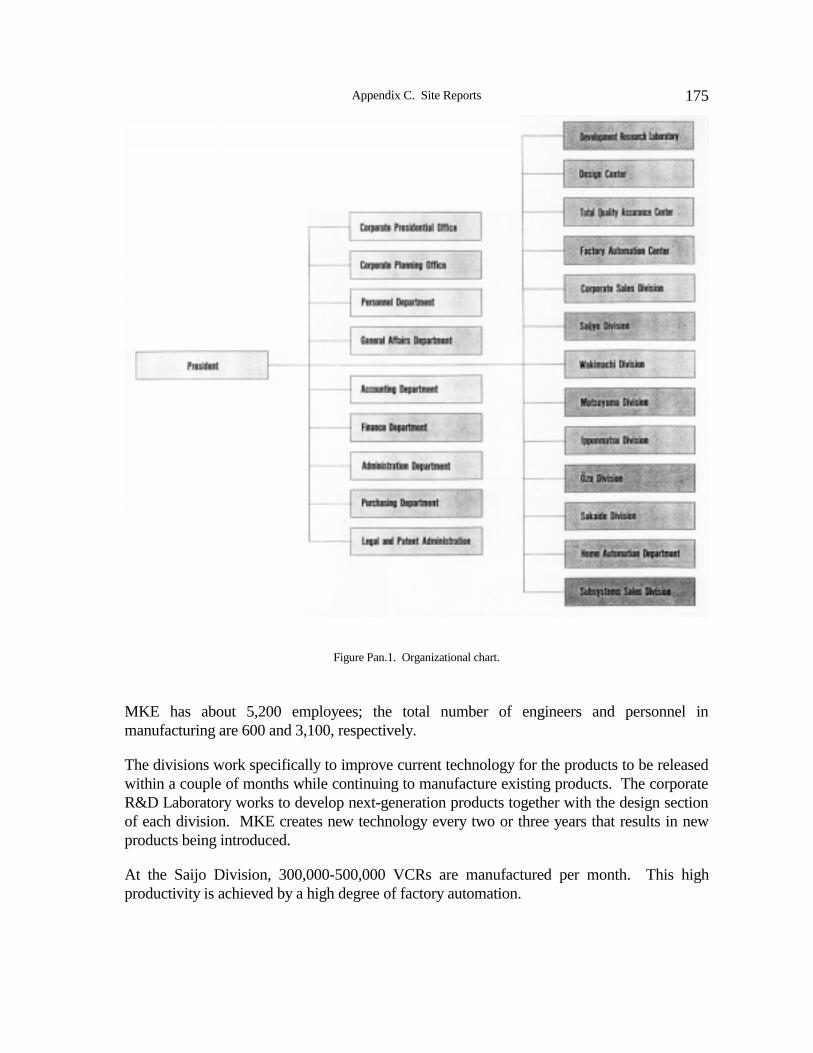
Appendix C. Site Reports 175
Figure Pan.1. Organizational chart.
MKE has about 5,200 employees; the total number of engineers and personnel inmanufacturing are 600 and 3,100, respectively.
The divisions work specifically to improve current technology for the products to be releasedwithin a couple of months while continuing to manufacture existing products. The corporateR&D Laboratory works to develop next-generation products together with the design sectionof each division. MKE creates new technology every two or three years that results in newproducts being introduced.
At the Saijo Division, 300,000-500,000 VCRs are manufactured per month. This highproductivity is achieved by a high degree of factory automation.
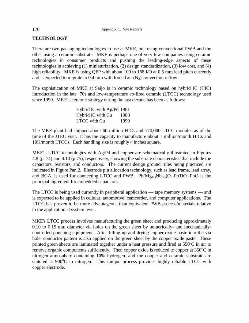
Appendix C. Site Reports176
TECHNOLOGY
There are two packaging technologies in use at MKE, one using conventional PWB and theother using a ceramic substrate. MKE is perhaps one of very few companies using ceramictechnologies in consumer products and pushing the leading-edge aspects of thesetechnologies in achieving (1) miniaturization, (2) design standardization, (3) low cost, and (4)high reliability. MKE is using QFP with about 100 to 168 I/O at 0.5 mm lead pitch currentlyand is expected to migrate to 0.4 mm with forced air (N2) convection reflow.
The sophistication of MKE at Saijo is in ceramic technology based on hybrid IC (HIC)introduction in the late ‘70s and low-temperature co-fired ceramic (LTCC) technology usedsince 1990. MKE’s ceramic strategy during the last decade has been as follows:
Hybrid IC with Ag/Pd 1981Hybrid IC with Cu 1988LTCC with Cu 1990
The MKE plant had shipped about 60 million HICs and 170,000 LTCC modules as of thetime of the JTEC visit. It has the capacity to manufacture about 1 million/month HICs and10K/month LTCCs. Each handling size is roughly 4 inches square.
MKE’s LTCC technologies with Ag/Pd and copper are schematically illustrated in Figures4.8 (p. 74) and 4.10 (p.75), respectively, showing the substrate characteristics that include thecapacitors, resistors, and conductors. The current design ground rules being practiced areindicated in Figure Pan.2. Electrode pin allocation technology, such as lead frame, lead array,and BGA, is used for connecting LTCC and PWB. Pb(Mg1/3Nb2/3)O3-PbTiO3-PbO is theprincipal ingredient for embedded capacitors.
The LTCC is being used currently in peripheral application — tape memory systems — andis expected to be applied in cellular, automotive, camcorder, and computer applications. TheLTCC has proven to be more advantageous than equivalent PWB process/materials relativeto the application at system level.
MKE's LTCC process involves manufacturing the green sheet and producing approximately0.10 to 0.15 mm diameter via holes on the green sheet by numerically- and mechanically-controlled punching equipment. After filling up and drying copper oxide paste into the viahole, conductor pattern is also applied on the green sheet by the copper oxide paste. Theseprinted green sheets are laminated together under a heat pressure and fired at 550oC in air toremove organic components sufficiently. Then copper oxide is reduced to copper at 350oC innitrogen atmosphere containing 10% hydrogen, and the copper and ceramic substrate aresintered at 900oC in nitrogen. This unique process provides highly reliable LTCC withcopper electrode.
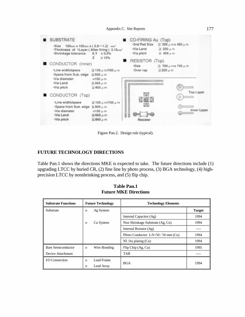
Appendix C. Site Reports 177
Figure Pan.2. Design rule (typical).
FUTURE TECHNOLOGY DIRECTIONS
Table Pan.1 shows the directions MKE is expected to take. The future directions include (1)upgrading LTCC by buried CR, (2) fine line by photo process, (3) BGA technology, (4) high-precision LTCC by nonshrinking process, and (5) flip chip.
Table Pan.1Future MKE Directions
Substrate Functions Future Technology Technology Elements
Substrate o Ag System Target
Internal Capacitor (Ag) 1994
o Cu System Non Shrinkage Substrate (Ag, Cu) 1994
Internal Resistor (Ag) ----
Photo Conductor L/S=50 / 50 mm (Cu) 1994
NI /Au plating (Cu) 1994
Bare Semiconductor o Wire Bonding Flip Chip (Ag, Cu) 1995
Device Attachment TAB ----
I/O Connection o Lead Frame
o Lead ArrayBGA 1994
Appendix C. Site Reports178
Site: Meisei University2-590 Nagafuchi, Ome-shiTokyo 198, Japan
Date Visited: October 8, 1993
Report Author: W. R. Boulton
ATTENDEES
JTEC:
P. BarelaW.R. Boulton
HOSTS:
Dr. Otsuka
BACKGROUND
Dr. Otsuka recently retired from Hitachi to assume a position at Meisei University, where heteaches a course on advanced information technology. He is affiliated with IEEE and chairedthe VLSI workshop held in Kyoto December 1994. He teaches computer and computerpackaging technology. Through workshops, he teaches engineers from Japanese companies.He has research contracts on electrical characterization of packages.
PACKAGING TECHNOLOGY IN JAPAN
Dr. Otsuka limited his formal remarks to the topic of "Main Packaging Technology in Japan(Single Chip Packaging)." He provided a number of important insights into the futuredevelopments of electronic packaging technology in Japan.
Korea or America is expected to take over long-term leadership in LCD packagingtechnology.
Dr. Otsuka made it clear that LSI packaging technologies have a different origin and corecompetence than LCD packaging technologies. The development of LCD technologies hascome from the merging of TV cathode tube and silicon wafer process technologies, whichgives Koreans and Americans the potential to take leadership in this area. Korea has made astrong commitment to LCD development, and recently, Samsung and Gold Star haveannounced massive investments of $400 million and $300 million, respectively, in TFTtechnology development programs through 1995.

Appendix C. Site Reports 179
Dr. Otsuka was not optimistic about Japanese companies maintaining leadership in CDtechnology. He didn't feel that large Japanese companies could work with small companiesto develop such a new infrastructure. At the time, large companies were worried about smallcompanies competing with them. Dr. Otsuka believed that Japanese companies' departmentalstructures were too competitive with each other to cooperate on merging new technologies.He felt that presidents cannot control their department heads. That means that they cannotdevelop large-scale systems like Apple did with Macintosh.
Small companies also provide a threat to large companies by their dedication to a singletechnology. While big companies are investing in CRT technology, they cannot give thesame effort to new LCD technology. The large companies are worried about the potential ofsmall companies. Active matrix LCDs by Japan Hosiden are a threat to Sharp because theyare selling to Apple and other U.S. companies like Boeing. Companies like Sony areintegrating backwards into their own components to increase profitability. That is causing abreakdown in supplier relationships and causing less coordination on new development.
In the future, Dr. Otsuka sees the United States maintaining strength in high-frequencydevices like computers and microprocessors. He expects Korea will be strong in memoriesand LCDs in the future. Low-cost micro assembly applications will remain the strength ofJapan in the future. If Japan loses low-cost QFP packaging technology, then he expects thatJapan will be in trouble. Since plastic molded lead frame packages represent 85% ofelectronic product applications, Japan's electronic industry must continue to lead in this area.
Japan will remain the leader in LSI packaging technologies.
Dr. Otsuka said that over 85% of electronic packaging uses plastic molded lead frametechnologies. Because these packaging technologies are so pervasive in Japanese industryand because so many companies are committed to them, he argues that Japan will continue todominate in low-cost packaging technology. LSI packaging technologies include materials,parts, subassemblies, and assembly process. Most companies have specialized in specificareas of plastic packaging technology, which provides Japan with the strongest low-costpackaging infrastructure. This infrastructure is distributed across both large and smallcompanies in Japan and, because it is pervasive, is unlikely to change its technologicaldirection. He pointed out that it would be virtually impossible for any one company or groupto change the technological focus of this infrastructure. Dr. Otsuka argued that, as a result,the low-cost electronic packaging industry in Japan will continue to develop current plasticpackaging technology, because it is the easiest direction for all industry participants tocontinue in.
Low cost is top priority in the Japanese industry, which requires mass productiontechnologies.
Because of Japan's cost requirements, Dr. Otsuka argued that LSI plastic packagingtechnology has to utilize mass production technology. This mass production orientation will
Appendix C. Site Reports180
continue to utilize existing packaging technologies. New technologies will require new massproduction technologies, which would be expensive to develop and lead to higher costs. Tokeep from incurring such added costs, Dr. Otsuka argued that companies will continue topush existing packaging technologies to their limits rather than add new high-costtechnologies. This strategy means that Japanese companies seek to solve performanceproblems related to current plastic packaging technologies.
Current plastic molded package technologies will meet future miniaturizationrequirements.
Dr. Otsuka feels that QFP packages can be designed with 0.15 mm pin pitch. Such fine pitchwill allow 800 pins on a 32 mm package, or 1000 pins on a 40 mm package, or 384 pins on a16 mm package. To support his argument, Dr. Otsuka gave examples of developments thatare currently under production or development in Japan. He provided an example of 344pins on a 28 mm package using 0.3 mm pin pitch that is currently in production at Hitachi.
Dr. Otsuka argued that Japan's strength is due to the extensive infrastructure of companiesinvolved in plastic electronic packaging technology. Japanese companies have developedQFP packages with 500 pins, available from Nippon Printing Company by 1996, using 0.3mm pin pitch. Some firms are currently developing this process using 0.2 mm pin pitchchips. This will allow plastic QFP packages to surpass ceramic PGA packages in pin density.Such strong development power comes from Japan's massive investment in all areas ofplastic packaging technology. Nikkei Electronics described these developments in itsAugust 2, 1993 issue (p. 94).
Dr. Otsuka also described Kyushu Matsushita's 0.15 mm pitch soldering process that heexpects to be commercialized within several years. This process uses a solder precoat (supersolder) with the body being pushed down as infrared heat is applied. The company usessolder bumps to ensure contact, but staggers the bumps to minimize shorting. This processwould not require new machine technology for production utilization. Kyushu Matsushita isplanning to use this approach in its next-generation camcorder production. While it iscurrently using TAB technology, Dr. Otsuka believes that the approach will be used withSMT in the future. Hitachi is currently producing circuits with 90 micron wire bonding onchips with spaces between the wire of 120 microns. Oki and Nippon Steel havedemonstrated wire bonding with 40 micron pitch. Dr. Otsuka believes that we will see thisin production in the future.
Fine pitch requires materials with higher resistivity. Fine pitch creates additional solderingproblems by causing high current on the printed circuit board. Dr. Otsuka suggested that newmaterials will be used on fine-pitch boards. For example, conventional FR-4 through-holeresistivity is too low at 130°C to be used on fine-pitch boards. High Tg epoxy provides betterresistivity, but for fine-pitch boards, the high resistivity requirements can be met with BTresin. Mitsubishi Gas Chemical has used BT resist (BTM 450) on contacts with 1.27 mmseparation.
Appendix C. Site Reports 181
Japan will overcome low yield problems caused by fine pitch packages. Dr. Otsuka agreedthat the move to fine pitch production will cause higher reject rates in the beginning.However, he argued that Japan has a long history of taking lower yield technology andimproving it. In the United States, he believes that companies change technologies if theyhave low yields, but not in Japan. In addition, QFP is more inspectable than BGA even inlow yield situations. Inspectability is very critical to ensuring quality products.
Finer pitch packages will automatically improve operating characteristics.
Fine pitch will increase product design flexibility. Since height is very important, single-layer boards are preferred in package design. Also, single boards are simpler to produce andare therefore cheaper to produce. Fine-pitch soldering would mean that we do not need two-layer bonding systems. Two-layer bonding has lower reliability because it depends on thesolder connections. Simple packages are the best in every characteristic. For 0.3 mm pinpitch, a 40 mm2 QFP package can have over 500 pins. With 0.2 mm pin pitch, 34 mm2
packages can have 600 pins. At 0.15 mm pin pitch, we can have 600 pins on a 28 mm2
package, comparable to a 1.0 mm pitch bump BGA chip. Dr. Otsuka used the previousexamples to argue that these dense packages will be available within this decade.
Fine-pitch packages will provide additional advantages. Dr. Otsuka pointed out that finerpitch allows the use of three-set wiring design instead of two-set wiring between ground andpower leads. Three-set wiring can increase output from 80-90 Σ to 95-105 Σ at 200 MHz andabove. Finer pitch allows use of three-set packages for high-power packages. At the sametime, impedance can be reduced once pin pitch falls below 0.3 mm. Japanese researchershave simulated 0.05 mm pin pitch designs and found that impedance drops 50%. Couplingcapacitance can be further reduced in fine-pitch applications by using shorter wires. Shorterwires also means that multilayer wiring in single-chip packages is not essential. As long aspower consumption stays below three watts per chip, chip scale packaging with short wiresand fine-pitch provide the best design solutions. This has already been utilized in memoryDRAM developments and should be viable in LSI packaging. As long as powerconsumption stays under 3 watts, natural cooling systems can be used and costs kept lower.
Dr. Otsuka also pointed out that reduced voltage requirements and reduced load capacitancecan save power consumption (P=1/2*CV2). Lower voltage reduces coupling noise. He thenargued that as we reduce package size, everything improves: "If we can communicate MHzat 3.3 volts, then the same package using 1.5 volts can operate at 400 MHz." He believes thatQFP chip scale packages will be able to pass 200 MHz in the future.
QFP will be competitive with BGA on price-performance measures. Dr. Otsuka believes thatQFP packages are better than BGA packages because they are inspectable and don't requirenew assembly technology. While the U.S. is interested in BGA because of its high pin count,Dr. Otsuka believes that 0.15 mm pin pitch on QFP packages will make them competitivewith BGA alternatives. Since most Japanese companies do not have BGA capabilities, he
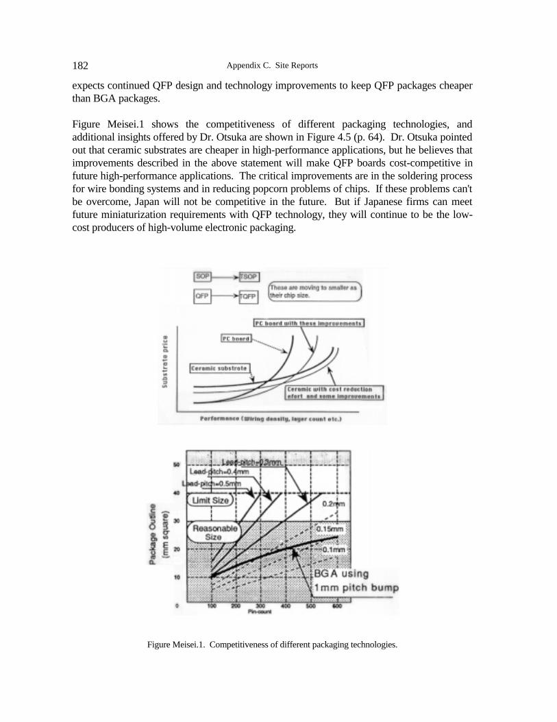
Appendix C. Site Reports182
expects continued QFP design and technology improvements to keep QFP packages cheaperthan BGA packages.
Figure Meisei.1 shows the competitiveness of different packaging technologies, andadditional insights offered by Dr. Otsuka are shown in Figure 4.5 (p. 64). Dr. Otsuka pointedout that ceramic substrates are cheaper in high-performance applications, but he believes thatimprovements described in the above statement will make QFP boards cost-competitive infuture high-performance applications. The critical improvements are in the soldering processfor wire bonding systems and in reducing popcorn problems of chips. If these problems can'tbe overcome, Japan will not be competitive in the future. But if Japanese firms can meetfuture miniaturization requirements with QFP technology, they will continue to be the low-cost producers of high-volume electronic packaging.
Figure Meisei.1. Competitiveness of different packaging technologies.
Appendix C. Site Reports 183
Dr. Otsuka believes single-chip packages will be cheaper than integrated chips on a substrate.He believes pushing the current technology to the limits will be cheaper than introducing newtechnology. Japan has alternative technologies, but low-cost plastic package technology ismuch cheaper. However, if package technology cannot achieve its improvement objectives,then its cost will cross over, and multichip technology will be cheaper.
Several technologies are unlikely to become dominant. Dr. Otsuka felt that adhesiveconductors create too much noise and are too low in quality to replace solder connections. Hecontinued to argue that the simple technology will survive. Reduction in size will reduce theproblems of solder pollution and allow high-quality alternatives to be used. Becauseminiaturization will require less solder, it will be cost-effective.
Japanese companies guarantee everything about their products. Dr. Otsuka believes that theywill continue to provide complete packages instead of bare chips. They want to control theassembly of their components to ensure their performance.
SUMMARY
Cost is the First Objective
There are three strategic objectives in Japanese competitive strategy. Since the mid-1980s theacronym "QCD" has been pervasive among Japanese companies: it stands for quality, cost,delivery.
All Japanese electronics suppliers are forced by their customers to keep lowering their costs. At the lowest cost, the company that provides the highest quality with the best availability ordelivery wins sales. This puts great pressure on firms to reduce costs and improve quality asa daily activity. It also makes it extremely difficult for Japanese suppliers to make a highprofit.
Miniaturization is Driving Automation
Sony has been driving consumer products technological development in Japan since the mid-1980s when it introduced the minicamcorder. It has set the rules of the game fordevelopment by projecting that the next model be half the size and half the cost for the samefunction. For example, its first minicam was 1.6 kg, its second was 0.8 kg, and the mostrecent was 0.4 kg. The current technology driver is the cellular telephone at 0.2 kg. Thesesmall-sized products are pushing product components and packaging technologies to smallersizes.
Continued commitment to the miniaturization of products and component technologiesrequires increased investment in production technologies and factory automation. As partsizes shrink, human assembly is no longer feasible. This has pushed assembly technologiesto become more precise and faster. For example, precision robots have improved
Appendix C. Site Reports184
repeatability precision from 0.05 mm to 0.01 mm since the mid-1980s. Matsushita's newSMT machine has 11 placement heads with 0.01 mm repeatability. Sony's high-speed robotsare now working at 0.012 repeatability placement.
Miniaturization and Automation are Increasing Competitive Advantage
Japanese companies have been committed to miniaturization for nearly a decade. Productminiaturization is leading to improved product operating characteristics. Smaller componentsizes lead to lower power usage and heat generation and longer battery life. Automation hasled to improved quality and faster delivery of new products. Sony's factory automationactivities have caused defect rates to drop to 20 ppm and have reduced ramp-up time to halfthat of manual assembly facilities. The goal of miniaturization has been supported byconcurrent engineering in both product and process technology development. Companieshave invested heavily in process technologies to achieve the miniaturization goals that can nolonger be achieved through manual production techniques. By developing existingtechnologies rather than investing heavily in new technologies, they have been able to keepoverall costs down and have stayed competitive in advanced consumer products.
High Technology is Only Used When Required
Japan's electronic packaging industry is heavily committed to plastic molded packagingsystems. Cost as a competitive objective leads Japanese electronics suppliers to avoid high-technology solutions to their miniaturization problems. Current QFP packaging technologiesare being pushed to their limits. Miniaturization of all components appears to be the strategy,not the movement to new technologies. New packaging technologies such as MCM are usedwhen needed, but are considered higher-cost than established technologies. Theminiaturization of current packaging technologies appears to be meeting the needs of mostproduct requirements.
At the same time, high-technology packaging solutions are available in Japan in high-performance products such as supercomputers. A recent study of supercomputers found thatHitachi had the most advanced design for future MCM applications. This suggests that costswill limit the use of such technologies except where current technologies fail to meet thefunctional or size requirements of the package.
GROUP COMMENTS MADE DURING THE DISCUSSION AT NCR
• Japan is using simple, low-cost technologies to win the market.
• Japan is committed to those simple technologies.
• Concurrent engineering is required for simultaneous product and process developments.
• Defense industries are driven by reliability and quality, and cause the cost to be high.

Appendix C. Site Reports 185
• Firms would be able to compete with Japanese firms if they were willing to make theinvestments. There are some production technologies that are not available in the UnitedStates. The equipment required for one micron of accuracy in miniaturized mechanicalcomponent production is probably outside of the U.S. capabilities today. We lack therequired skills. Japan does not have the technology required to make advancedmicroprocessors.
• The U.S. believes that it can go to the moon if the commitment is made. It would requirea number of years to rebuild the infrastructure and educate the people.
• The basic questions are, "What skills do we have? What do we want to do? Whatactions do we need to take to achieve those objectives?"
• All new products at the electronics show are smaller than the previous models. The onlyway that the U.S. will compete is to get into the market.
• The U.S. dominates the market in design tools and microprocessors. This should providesome opportunity for development. U.S. firms have designed but not exploitedtechnologies.
• Most firms produce their own equipment and plan to build even more of their equipmentin the future. The ability to produce is a constraint to getting into the business. Somefirms have developed their own equipment to sell their components. They use othermakers’ equipment, but build their own when equipment is not available to meet theirown needs. So why is TI selling off its equipment business?
• The companies we visited build a high portion of their own equipment and place a highpriority on production technology.
• Most firms said they were not going to get into BGAs, but would push today's technologyto the limit. Those firms going to TAB may be taking a high-cost alternative.

Appendix C. Site Reports186
Site: Murata Manufacturing Co., Ltd.2-26-10 Tenjin, Magaokakyo-shiKyoto 617, Japan
Date Visited: October 6, 1993
Report Author: M. Kelly
ATTENDEES
JTEC:
M. KellyG. LimN. NaclerioJ. Peeples
HOSTS:
H. Kuronaka Manager, R&D Management SectionH. Iwatsubo Assistant Chief, R&D Section
BACKGROUND
Murata is a leader in the production of discrete electronic components. The primary marketfor Murata products is Japan (63%), followed by the United States (11%), Europe (10%), andAsia (most of the remaining 16%). The company strategy is to pursue manufacturing withinthe geographical spheres of its primary customers. The Murata group includes 23,000employees and 47 affiliates, including 23 overseas; Murata Erie North America, for example,has two plants in Georgia, one of which makes capacitors and the other of which makespassive electronic components. Based on information contained in the 1993 annual report,the primary product groups in Murata are the following:
• Capacitors. This group produces monolithic disk-type and semiconductor ceramic andtrimmer capacitors.
• Resistors. This group produces PTC thermistors, potentiometers, R-networks and high-voltage resistors. Demand comes primarily from Japanese display manufacturers.
• Piezoelectrics. This group produces ceramic filters, ceramic resonators, piezoelectricbuzzers, and surface acoustic wave filters.
• Coils. This group produces flyback transformers, deflection yokes, and various types ofcoils. The major expansion was in sales of high-definition and microwave deflectionyokes for computer displays in the Japanese and Asian markets.

Appendix C. Site Reports 187
• Electronic Modules. This group produces circuit modules and power supplies. There hasbeen a high demand in overseas markets for voltage controlled oscillators for mobile andportable telephones.
• Other Products. There is a wide variety of “other products” that include EMI suppressionfilters, microwave filters, sensors, piezoelectric vibrating gyroscopes, thermal cutoffs, andproduction equipment. The most attractive markets are in the areas of EMI suppressionfilters for computers, piezoelectric vibrating gyroscopes for camcorders, and in the future,compact switching regulators (2 MHz) for notebook PCs.
Murata sales total about $2.7 billion annually, with capacitors representing 38% andpiezoelectric components 20%. We were told that Murata dominates world market share ofceramic filters/ceramic resonators (85%, $100 million/mo), capacitors (50%), thermistors(40%), and EMI suppressors (30%).
Murata’s product strategy is to continue to build on its strengths and move aggressively to bea supplier of complete functional modules. In pursuit of future objectives, Murata isspending 6.5% of sales, about $176 million, on R&D.
Murata’s primary R&D domains include
• microwave modules (for digital cordless telephones): oscillators, mixers, synthesizers,antennas, filters, GaAs MMICs
• power supplies (SW frequency 2 MHz): CAD, substrates, packaging, transformers,capacitors
• functional sensor modules: gyro sensors, IR sensor arrays, signal processing, technologyintegration
• capacitors (miniature, high capacitance): thin film multilayer, ceramic, reliability,electrode materials
• filters (for communications): piezoelectric ceramic products, high-Q ceramics, thin-filmprocess
Murata’s strategic technologies are identified in Figure 7.5 (p. 137). Other areas consideredimportant by Murata include module circuit application-specific components and verticaltechnology integration within the company.
As of the JTEC visit, recent capital investments had been made for the production of ceramicmaterials, monolithic ceramic capacitors, components for imaging equipment, chipcomponents, microwave components, and electronic modules. Aggressive capitalinvestments were also made for thin-film processing technology and the development ofequipment for gallium-arsenide semiconductor devices.

Appendix C. Site Reports188
At the time of the JTEC visit, Murata planned to have a gallium-arsenide integrated circuitpilot line in production by the end of 1994. The motivation for establishing the line, asexpressed by our hosts, is to protect intellectual property and to improve Murata’scompetitive posture in the microwave and RF module business by focusing on futurepersonal communication products.
Murata is doing extensive work in sensor development. Present applications for sensorproducts include engine knock detectors and fire and burglar alarms. An advanced sensorapplication that was discussed is a piezoelectric gyro for sensing angular accelerations. Thecurrent product measures 21.5 x 8 x 8.5 mm and is used in the Sony TR2 and TR3 palm-sized camcorder for vibration stabilization. A larger, more accurate version (24 x 24 x 58mm) is used in Pioneer’s automobile GPS navigation systems. Future markets for Muratasensors include accelerometers and chemical/gas detection.
A new silicon micromachining program has been initiated at the Yokohama R&D Center todevelop microminiature accelerometers, sensors, and oscillators.
The manufacturing lines JTEC panelists toured in Kyoto are most impressive. The totalprocess is automated. The equipment appears to be very robust and capable of handling veryhigh-volume throughput. Over 80% of the equipment being used was designed and built byMurata. Much of the equipment is customized to meet specific product requirements, whichjustifies the in-house development; however in more general terms, Murata recognizes theimportance of internal equipment development in order to protect its competitive advantages.There was evidence of continuous improvement in the manufacturing processes, withparticular emphasis on equipment improvements.
Murata has evidently mastered the manufacturing process for high-volume, miniaturizeddiscrete components. Perhaps this explains its dominance in the world market. There wasnothing magic about what we saw: outstanding equipment designed for automation,meticulous attention to detail, continuous improvement, qualified personnel, and a committedmanagement team.
It became very evident during our discussions that Murata places a very high priority oncustomer interactions. It was pointed out that in some cases Murata people visit customersonce or twice a day. Procurement planning is regularly updated, and Murata can expect atleast a three-year lead time from customers for new product requirements. It was likewiseevident that the needs of suppliers were taken into account when negotiating reduced costs.Suppliers, it was stated, are no good to us if they are driven into bankruptcy. Suppliers areconsidered part of the team and expected to contribute to the competitiveness of the product.
The visit to Murata substantiated much of what has been identified as Japanese strengths:
• Focus on the fundamentals
• Pursue continuous improvements

Appendix C. Site Reports 189
• Drive continuously to miniaturize components
• Work closely with suppliers and customers
• Design and build your own equipment
• Eliminate waste
• Make cost reduction a primary objective in design and manufacturing
• Automate whenever it is cost-justified
• Build on core competencies
• Follow an evolutionary product strategy
• Move increasingly to integrate components to produce functional modules
Murata, like other Japanese companies visited, was concerned about the effects of therecessionary period that industry was experiencing at the time of the JTEC visit. The attitudeof our hosts, however, was very positive about the future of Murata. If anything, I expect thatthe present economic climate will strengthen the company and better prepare it for thecompetitive challenges of the future.

Appendix C. Site Reports190
Site: Nippondenso Kota PlantNippondenso Co., Ltd.1-1 Shawa-cho, Kariya-shiAichi-ken 448, Japan
Date Visited: October 7, 1993
Report Author: N. Naclerio
ATTENDEES
JTEC:
M. KellyN. NaclerioJ. Peeples
HOSTS:
Mizutani Shuji Director, Automotive Electronics DivisionShigehiko Ito General Manager, Electronics Manufacturing Dept.Mark R. Hunter Public Affairs Department
BACKGROUND
Nippondenso is a leading manufacturer of automotive components and electronic systems. In1992, Nippondenso had sales revenues of about $12 billion. Approximately 9% of sales wasinvested in capital and another 7.3% in R&D. About 56,718 people were employed byNippondenso in 1992. (The above figures are based on consolidated 1992 data.)
Some of the themes that drive Nippondenso's business strategy are high performance, safety,and fuel efficiency. In-house research ranges from semiconductors to micromachines tomaterials, and from AI to telecommunications to control theory. Fuzzy logic systems havebeen developed and are in use for anti-lock braking systems (ABS), cruise control, andsuspension systems. Nippondenso uses its micromachine technology to manufactureaccelerometers and other sensors for automotive applications. As a demonstration of itsmicromachine prowess, it built a miniature car, barely 5 mm long, complete with electricmotor. Nippondenso plans to fuse automobile technology with state-of-the-art electronics togenerate new products in many fields. Examples of nonautomotive products we saw includedportable cellular phones, hand-held bar code scanners, and factory automation systems.
Nippondenso manufactures components and systems for nearly every automobilemanufacturer in the world. While Toyota is its largest shareholder and customer, it also sellscomponents to most of the other Japanese auto makers, the Big Three U.S. companies, and
Appendix C. Site Reports 191
most European companies. Nippondenso claims to be a leader in 14 product areas includingelectronics, fuel injection systems, braking control, navigation, air conditioners, fuel pumps,and radiators. Nippondenso product groups do their own product development andmanufacturing but do not have their own sales forces since most of their products are sold toa few automobile companies.
THE KOTA PLANT
Activities at the Kota plant include manufacture of automotive ICs, electronic control units(ECUs), and communications equipment. This plant is located in Aichi Prefecture on274,000 m2 and was dedicated in April 1987 after one year of construction. The site is about50% developed, with three main buildings. A new wafer fabrication facility occupies about18,000 m2 of floor space, and a four-floor electronics factory occupies 173,000 m2. The totalvalue of the products manufactured in the Kota plant in 1992 was about $160 million permonth. There are approximately 5,000 pieces of equipment and 3,700 employees.
IC Manufacturing
Nippondenso's IC production is being transferred from a 5" line at the head office in Kariya toa new 6" line at the Kota plant. Nippondenso has been in the IC business for 25 years. Whileits people recognize that they cannot compete with large merchant IC companies in productslike general purpose microprocessors or memories, they still feel that in-house ICmanufacturing gives them a competitive advantage. Two advantages of building devices in-house cited by Nippondenso are (1) the ability to produce specialized products not availableon the market, and (2) the ability to avoid sharing proprietary designs with potentialcompetitors. Nippondenso manufactures complex, more expensive VLSI chips that arespecially designed for automotive applications.
Engine Control Unit Assembly Line
The main four-story building at the Kota site houses chip assembly, hybrid manufacture,SMT board, and final assembly. Five different engine controller product families includingover 120 different engine controllers are made on a single assembly line. The line beginswith traditional surface mount assembly including adhesive application, component pick-and-place, add form component assembly, and test. After testing, a conformal environmentalcoating is applied to the boards. The boards are then assembled into metal enclosures that aresealed and marked. The completed modules go through high-temperature burn-in beforefinal outgoing test. After testing, the modules go into a stocker on the factory floor to await adaily shipment to nearby Toyota automobile assembly plants.
The entire 1,170-meter manufacturing line, including assembly, burn-in, and test, has onlyone direct labor worker who folds multiple rigid boards connected by flex cables into a metalenclosure. We were told that this operation had not been automated because the necessarymachine would be too expensive. There is zero changeover time between products on the
Appendix C. Site Reports192
line. In fact, we were told that complex and relatively simple engine controllers wereintentionally mixed to balance the throughput of the line. As a practical matter, controllersare usually made in batches of 16 since that is the size of the cassettes used to transportboards on AGVs. In order to simplify material handling, all of the products have a commonwidth, but appeared to vary in length by as much as a factor of three. Every board type isidentified by a bar code, and every piece of equipment on the line has its own bar code reader.As a result, the number of different components that must be simultaneously loaded on thepick-and-place machines is probably higher than on most lines producing only one product ata time.
Production Systems
Almost all of the manufacturing equipment we saw at the Kota plant was produced internallyby Nippondenso. Our hosts claimed that because of the company’s unique needs, it isactually cheaper to develop equipment in-house rather than purchase more general-purposetools. One tool for visually inspecting solder joints reportedly took over two years to developinternally. Over 200 people at the Kota site are involved in the development of productionequipment and processes. The average piece of equipment on the manufacturing line is eitherreplaced or upgraded every three to four years. Some of the larger pieces of factoryequipment are developed at another Nippondenso site dedicated entirely to that purpose, butmany of the smaller pieces of equipment are developed and manufactured on-site. In allcases, customization of the equipment, fixture development, and programming is theresponsibility of the manufacturing site. Nippondenso is just beginning to market productionequipment such as robots to external customers. Factory equipment and production processesare designed by teams that include both hardware and software engineers. The Kota plantwas the first to implement a factory-wide CIM system, now in place at all other plants. Thissystem unites data from the head office and all the factories to meet quality standards anddelivery times. (In addition to factory-level data, information from design and sales is alsoincluded.)
Multichip Modules
We saw some ceramic MCM modules or hybrid assemblies built at this plant using flip-chipassembly. The flip chip used is similar to that employed by some U.S. automotivemanufacturers and involves plated copper bumps with solder. The main Japanese concernwith the wider use of MCMs is reportedly cost. Nippondenso says that MCM-L is very closeto introduction in some of its automotive applications. Its automotive customers are not tooanxious to have risky "new" technologies used in their cars; however, Nippondenso thinksthat MCM-L will be the lowest-cost solution for many ECU products.
Another driver for the use of MCM technology will be miniaturization of engine controlfunctions so that they can be mounted directly on sensors and/or actuators. Nippondensorepresentatives feel that by 1998 multiple functions will be combined into modulescontaining sensors, processors, and actuators. These distributed processors will share dataacross a vehicle-wide network.

Appendix C. Site Reports 193
Impact of Automation on Productivity
The highly automated production line at Kota results in a high degree of flexibility, very highmanufacturing quality, and the elimination of most direct labor. During the time the JTECteam spent in the ECU assembly plant, we did not see any modules in reject bins. Accordingto one host, only a couple of modules per month fail final test. In five years Nippondensoexpects to have added a second wafer fab and 50% more assembly area while also hoping toreduce by half the total number of people on the site to less than 2,000 from the current 3,700.
Customer Relationships
Nippondenso has close ties to its automotive customers. Large customers provide regularlyupdated five-year production requirements. Engine control units are essentially built to orderand delivered to customers every day. In order to provide similar service to North Americanauto makers, Nippondenso operates a similar assembly line in the United States.
Engineer Training
Nippondenso runs its own two-year college for training engineers. Managers tend to holdfour-year degrees from university engineering programs. Practical training in areas such asequipment design takes place almost entirely within the company. During the first five yearsof employment, engineers each receive about 100 hours per year of formal technical trainingresulting in the equivalent of a master’s degree. In the sixth year, about 10% of the engineersare selected for the management track and receive another 200 hours of technical training.After ten years about 2-3% are selected to become assistant managers and receive additionaltraining. By this point, the assistant managers have earned the equivalent of a Ph.D. withinthe company. Management and business training is also provided for those technicalmanagers. The fraction in nonengineering fields who become managers is perhaps 10%.
Display Technology
Nippondenso manufactures passive liquid crystal displays (LCDs) for black-and-whiteinstrument displays. It also manufactures a holographic display produced for the Lexusautomobile that projects the vehicle's speed two meters in front of the windshield.Nippondenso’s R&D labs have very recently developed a color anti-ferroelectric LCD displaytechnology that offers a wide viewing angle and the potential to be very low-cost. A ten-inchdiagonal display suitable for personal computer applications has already been demonstrated.
Future Directions
Nippondenso believes that future automobiles will contain highly integrated, but distributed,electronic systems composed of sensor/processor/actuator modules that share data over avehicle network. When asked about the role of fiber optics in those automobiles, our hostsresponded that the company’s experience putting optical fiber links in the Toyota Sentry doorlock system taught them that optical data links are too expensive for automobile applications;Nippondenso was no longer pursuing them at the time of the JTEC visit.

Appendix C. Site Reports194
Nippondenso is already shipping highly integrated communication/navigation/entertainmentsystems for luxury automobiles. A demonstration at the plant showed a new system beingmanufactured for the Lexus automobile. A color flat-panel display built into the automobile'sconsole can display television when the car is parked. While driving, it can be used todisplay map information or travel guides from CD ROM. The system can also displayposition information obtained from an automotive navigation system that includes both GPSand dead-reckoning. The dead-reckoning system uses wheel rotation information from theABS sensors in the front wheels of the car. When the car is put in reverse, a CCD camerashows what is behind the car. If the car gets too close to another vehicle or obstacle, awarning is flashed on the screen. An FM-broadcast traffic information system was scheduledto begin pilot operation in Japan in 1994, allowing the car navigation system to also displaytraffic congestion information. Aftermarket GPS/navigation/entertainment systems are alsobeing produced by a number of other Japanese electronics companies including Sony,Matsushita, and Pioneer, and they are reportedly very popular with young Japanese.
SUMMARY
Nippondenso is a best-of-breed automotive electronics manufacturer. It manufactures vehicleelectronic systems for sensing, control, communications, and navigation. Perhaps as a resultof its close relationship to Toyota, it has embraced a flexible manufacturing approach thatenables it to manufacture engine control units with a lot size of one and zero changeovertime. This flexibility does not appear to cost the company in-line throughput ormanufacturing quality, both of which appear to be world class. Like other large Japaneseelectronics companies, Nippondenso is vertically integrated, and it designs and manufacturesmost of its own production equipment. Because of its unique approach to flexiblemanufacturing, it is possible that in-house development of production equipment such asSMT assembly is actually cheaper than purchasing full-featured machines on the openmarket. Nippondenso manufactures key components such as semiconductors andmicromachined sensors because of the view that doing so gives it a proprietary advantage.The use of MCM technology at Nippondenso will be driven by cost reduction and the desireto integrate sensors, processors, and actuators into compact modules that can be locateddirectly on engine and drive train systems.
Most formal training of engineers takes place in-house, with all engineers receiving 100-200hours of formal technical training per year. The company’s skills as a low-cost producer ofvery high-quality electronic systems is enabling it to branch out into other markets such aspersonal communications and mobile point-of-sales terminals.
Nippondenso believes that total manufacturing efficiency can only be achieved by closelycoordinating product development with production engineering. To achieve this,Nippondenso has long been developing specialized manufacturing equipment and methodsin-house.

Appendix C. Site Reports 195
Site: Nitto Denko Corporation61-7, Aza-Sasadani, Yamadera-choKusatsuShiga 525, Japan
Date Visited: October 6, 1993
Report Author: G. Harman
ATTENDEES
JTEC:
W. BoultonG. HarmanG. MeieranM. PechtD. Shelton
HOSTS:
M. Takemoto General ManagerY. Takashima ManagerM. Sano Manager, Design SectionS. Omori Manager, Quality AssuranceH. Tabada Chief Researcher, Reliability Evaluation CenterT. Mitarai Assistant Manager, Overseas DepartmentM. Kaneto Researcher
BACKGROUND
Nitto Denko is a diversified materials company with headquarters in Osaka. Nitto Denko'sphilosophy is to listen to the customers who are on the leading edge of technology and todevelop or improve products for their use.
The company was founded in 1918 to produce electrical insulating materials in Japan. Eachproduct center has its own development group and profit center and issues its own financialreport. Nitto Denko is an independent company, not part of any keiretsu. About 30% of itsbusiness is semiconductor- and electronics-related. Other areas include industrial products,packaging products, engineering plastics, medical products and membrane products. NittoDenko is a major plastic molding-compound supplier for semiconductor chip encapsulation.Our hosts also indicated that Nitto is the major producer of polarizing films (used in flat paneldisplays) and low friction rings (used in floppy disks). The company's newest venture is toproduce cultured (fermented) ginseng soft drinks to help improve its profit margin. Nitto

Appendix C. Site Reports196
Denko has manufacturing plants for various products located all over the world, includingthree in the United States that will be expanding soon as the firm moves more production offshore.
Nitto Denko's philosophy emphasizes that it listens to its customers — a lesson that manyAmerican companies could learn. It has a standing committee to help solve applicationsproblems of companies using its products. Planning for future growth is exceptional.Company personnel have outlined the entire semiconductor assembly and packaging processand would like to develop products that will contribute to or simplify each step. A diagramshowing this approach is given in Figure Nitto 1. A further example of Nitto’s exceptionalplanning is its development and fitting of future products into the U.S. SIA roadmap forsemiconductor development by the year 2000. Our hosts at Nitto Denko stated that they havea department of "Research on New Basic Technology," but nothing we saw was identified ascoming from that. In fact, when asked how many Ph.D.s they have in this particular plant,their response was "only one." Before a recent reorganization they had four.
Figure Nitto.1. Nitto's technical development plan for semiconductor related materials.
Appendix C. Site Reports 197
Nitto’s Kameyama plant is highly goal-oriented. It has a product line that primarily consistsof adhesives and packaging and encapsulation materials. The company then looks for waysto apply these products and expertise to the field of electronics materials. The JTEC teamdiscerned no fancy gear or advanced research projects; just a strict "improve the product andlook for new areas to apply products," no-nonsense approach. The company is quite creativein looking for new applications, but in the electronics areas, it is not trying to expand itsproduct line into ceramic packaging. It is the company's understanding of the characteristicsof plastic materials that separates it from its competitors. Nitto appears to be a world leaderin this area.
Finances
Nitto had net sales of $2.187 billion with a net income of $34.3 million in 1993. Thiscompared with a net income of $55.7 million in 1992, and $71.3 million in 1988. The sharpdecline in 1993 resulted from the increased value of the yen, coupled with downward costpressure from its Japanese customers. It is planning to expand production overseas to helpovercome the effects of the increasing value of the yen.
The biggest problem facing Nitto is the flat sales volume for plastic molding compounds. Thevolume of molded plastic packages continues to increase, but the thinner packagedimensions, e.g., small outline devices, may be only 0.5 mm thick, and improved molddesign leading to reduced loss of plastic during the molding operation has led to flat sales. Itseems that both of these trends will continue in the foreseeable future. However, it is notobvious what can be done to improve this situation. Nitto has been a leader in developinglow-stress molding compounds as well as in low alpha particle filler materials, and it is wellpositioned to maintain leadership in these various technical areas, as well as in the newproducts mentioned below. Company officials hope that increased overseas production willovercome the flat sales and profits in the older product areas.
Specific Products
Nitto is developing a number of new products based on its core technologies. One suchproduct is a new die attach material for application to the whole wafer called "Elep Mount."This is a conductive epoxy film applied to the backside of the wafer before sawing. Thisapplication can save several assembly steps and thus time and money. (Note: This is an oldidea originating in the ‘70s at Fairchild. Early in the ‘80s, such films were unsuccessfullymarketed by Stauffer Chemical, a U.S. company, which sold that division to Ablestick. Thefilm is apparently not marketed now. Amicon also tried to market a conductive epoxyscreened-on-wafer variation of the system in about 1985. Both had technical problemsrelating to water pickup in the uncured resin during sawing, even if the wafer is not sawedthrough, which assembly people prefer to do. A water-repellent uncured epoxy film withnew specialized equipment, with IC manufacturing cost pressures, may make it successful forNitto.)

Appendix C. Site Reports198
Other semiconductor-related products were discussed. We requested information on aproduct called ASMAT. This is being developed by Nitto for an ARPA contractor (U.S.)who is planning to use it as area-array contacts for whole-wafer test and burn-in, to obtainknown-good-die. The contacts are hemispherical bumps, precisely electroplated (and/oretched) 48 µm in diameter on large two-metal layers of polyimide films. Nitto has a toughjob ahead to cover all of the obvious problems inherent in placing a contact-covered polymerthin film on hundreds/thousands of bond pads in a wafer, e.g., no metallurgical interactionwith the bond pad is permitted at burn-in times and temperatures, and the film contacts mustbe position-stable at all times and temperatures. Also, the contact resistance varies withapplied force, so each one of thousands may require its own, or at least regional separatespring loading. Nitto is considering plating the bumps with nickel, gold, rhodium, osmium,etc. It expected to publish a full paper on ASMAT at the ISHM symposium held inNovember 1993.
Other products in development included improved molding compound adhesion to palladiumplated leadframes, high-thermal-conductivity molding compounds for power devices, andothers that need lower thermal resistances. Ideally, these materials could be developed toreplace ceramic packages. Nitto is also working on recyclable molding compounds(presumably thermoplastics) and low-viscosity compounds intended to go under flip chips (aprocess developed by IBM). Nitto is also developing mold compound pellets that are dust-free for use in the future (class 100) clean-room assembly and packaging areas. Nitto is alsostudying trapping agents that can slow the migration of bromine ions (fire retardants) inmolding compounds and thus increase gold wire bond reliability. It is developing compoundsthat are stronger, have greater leadframe adhesion, and have lower moisture absorption, foruse in TSOPs (thin small-outlined packages). In addition, Nitto is developing materials thatrequire no post mold cure (currently such cure takes five to six hours at 175°C). It is usingthe Cornell University software for modeling its thermosetting plastics. Also beingdeveloped are lines of adhesive contacts and adhesive tapes for die attach, TAB assembly,flexible mounting for chip carriers, etc. It seems to have a well thought out strategy forapplying its specific technologies to the entire range of assembly and packaging needs of theindustry.
PLANT TOUR
The Nitto Denko plant and much of the equipment was not new, but certainly appeared to beadequate for the job. The failure analysis and other materials analysis lab facilities appearedadequate, but by no means grandiose. There were all the important analytical andenvironment test facilities needed for evaluation of plastic packaged devices: IR microscope,SEM, radiography, EDX and WDX, TMA and TAG, pressure cookers, thermal cycle andthermal shock, etc. There were no super advanced capabilities such as advanced surfaceanalysis (Auger, STEM, ESCA, etc.), but the company seems to have access to thosecapabilities if needed. Our main impression of the analytical facilities is that they areextensively used. Work was going on in most of these facilities (which are located in one
Appendix C. Site Reports 199
large room.). Each piece of equipment was clearly labeled in English, apparently for thebenefit of the many visitors who come to the facility.
A large area is devoted to lead frame plastic molding equipment for running the manyexperiments necessary to develop new molding compounds. These experiments are designedby finite-element-modeling of the mold compound during molding to minimize wire-sweepand air bubbles. (Nitto may use some of the Cornell software imbedded in its own). Therewas considerable QA equipment available for testing the molding compounds (gelling time,rheology tests, spiral flow testing, etc.). We saw several examples of QA processes duringour tour.
The plant was typical of a chemical manufacturer rather than an electronic (clean-roomenvironment) manufacturer. This was especially evident in the areas where the moldcompound was formulated and pelletized. However, it should be emphasized that there wassufficient cleanliness for the products, and if more is needed, it will be supplied. The level ofautomation in the preparation of molding compound is not particularly high, but adequate forthe job.
Appendix C. Site Reports200
Site: Oki Electric Industry Co., Ltd.Honjo Plant1-1, 4-Chome, OjimaminiamiHonjo-shiSaitama 367, Japan
Date Visited: October 7, 1993
Report Author: J. Kukowski
ATTENDEES
JTEC:
P. BarelaJ. KukowskiL. SalmonR. Tummala
HOSTS:
Tohru Handa Executive Mgr, New Business Development Div., Telecommunications Group
Yoshinobu Tateishi Gen. Mgr, Honjo Plant, Tele. GroupYoichi Kohara Gen. Mgr, LSI Packaging Eng. Dept., LSI
Assembly Eng. Div., Electronic Devices GroupSaburo Iida Gen. Mgr, Tele. Devices Devt. Div., Tele. Network Gp.Yasuhide Ohnuki Mgr, Functional Devices Devt. Dept., Tele.
Devices Devt. Div., Tele. Network GroupJiro Utsunomiya Manager, Functional Devices Devt. Dept. Tele.
Devices Devt. Div., Tele. Network GroupMitsuhide Yamada Manager, Functional Devices Devt. Dept. Tele.
Devices Devt. Div., Tele. Network GroupYasuo Iguchi Research Manager, Microelectronics Dept. Research
Lab. R&D GroupToshiyasu Takei Manager, P.C.B. Eng. Dev. Sect. Takasaki Plant
Computer and Network Systems GroupAkihisa Yamada Manager, Eng. Relations Dept., Eng. Admin. Div.Hitoshi Shibuya Assist. Mgr, Functional Devices Devt. Dept. Tele.
Devices Devt. Div., Tele. Network Group
BACKGROUND
Oki Electric, Japan's first telecommunications manufacturer, was founded in January 1881. Itis developing its business globally, pursuing all aspects of research and development,
Appendix C. Site Reports 201
production, marketing, and service from an international perspective. The company’sbusiness sectors are telecommunications systems, information processing systems, andelectronic devices. The company produces a wide range of products that include switchingsystems, transmission systems, telecommunications terminals, data communications systemsand peripherals, underwater acoustic systems, telemetry and telecontrol systems, automotiveelectronics systems, and electronic devices. The company's vision is to capitalize on thetechnical strength of the three business sectors to be successful in the coming multimedia age.
HONJO PLANT
The Honjo manufacturing plant produces products for the telecommunications systemsbusiness sector. The products being produced at this site include asynchronous transfer mode(ATM) switching systems, modems, facsimiles, telephones, and other peripherals.
Technical Presentations
Detailed technical presentations were given on the following subjects:
• multichip modules
• polyimide-copper thin film multilayer substrate
• development of post-CFC cleaning technology defluxing
• development of single-PPM soldering systems
• LSI packaging technology
• packaging technology for fiber-optic devices Multichip Modules (MCM). The subject of MCM was presented by Mr. Iida. The topicscovered were benefits, Oki development direction, MCM structures, design specifications forLTCC and copper polyimide thin film multilayer substrate, Oki's implementation schedule,and identified applications.
Benefits
The benefits for creating a MCM are high speed, miniaturization, high reliability, and lowcost. The driving forces are low cost and high speed. The key issues in achieving low costand high speed have been identified as
• miniaturization, as well as monolysic LSI (large-scale integration)- very fine pattern of substrate- flip chip bonding
• assurance of known good die (KGD)
• concurrent design (board/module/LSI)
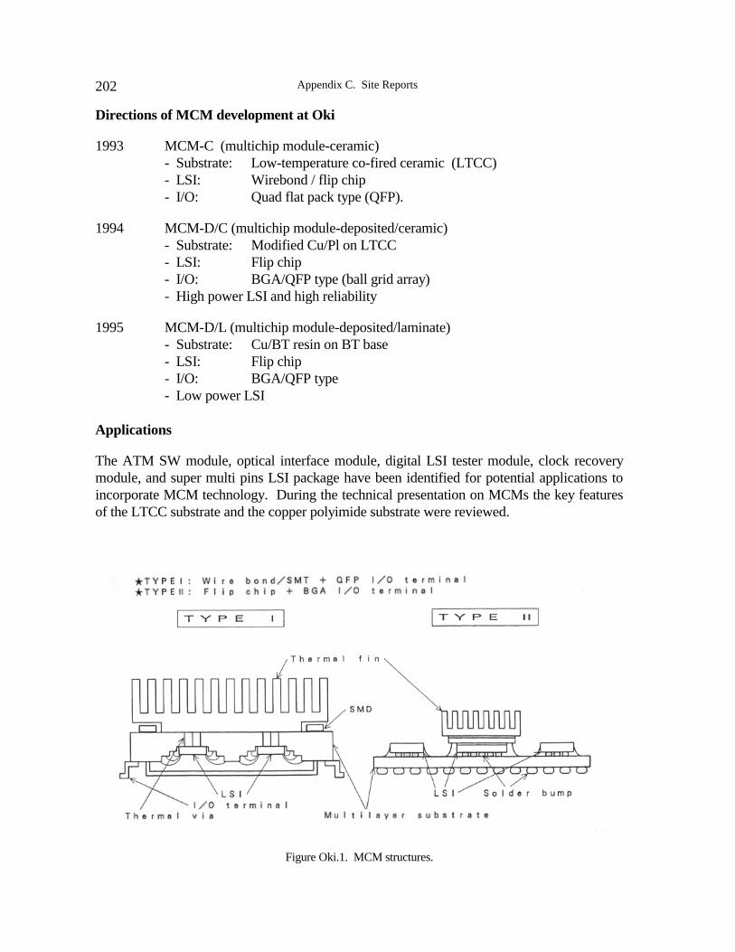
Appendix C. Site Reports202
Directions of MCM development at Oki
1993 MCM-C (multichip module-ceramic)- Substrate: Low-temperature co-fired ceramic (LTCC)- LSI: Wirebond / flip chip- I/O: Quad flat pack type (QFP).
1994 MCM-D/C (multichip module-deposited/ceramic)- Substrate: Modified Cu/Pl on LTCC- LSI: Flip chip- I/O: BGA/QFP type (ball grid array)- High power LSI and high reliability
1995 MCM-D/L (multichip module-deposited/laminate)- Substrate: Cu/BT resin on BT base- LSI: Flip chip- I/O: BGA/QFP type- Low power LSI
Applications
The ATM SW module, optical interface module, digital LSI tester module, clock recoverymodule, and super multi pins LSI package have been identified for potential applications toincorporate MCM technology. During the technical presentation on MCMs the key featuresof the LTCC substrate and the copper polyimide substrate were reviewed.
Figure Oki.1. MCM structures.
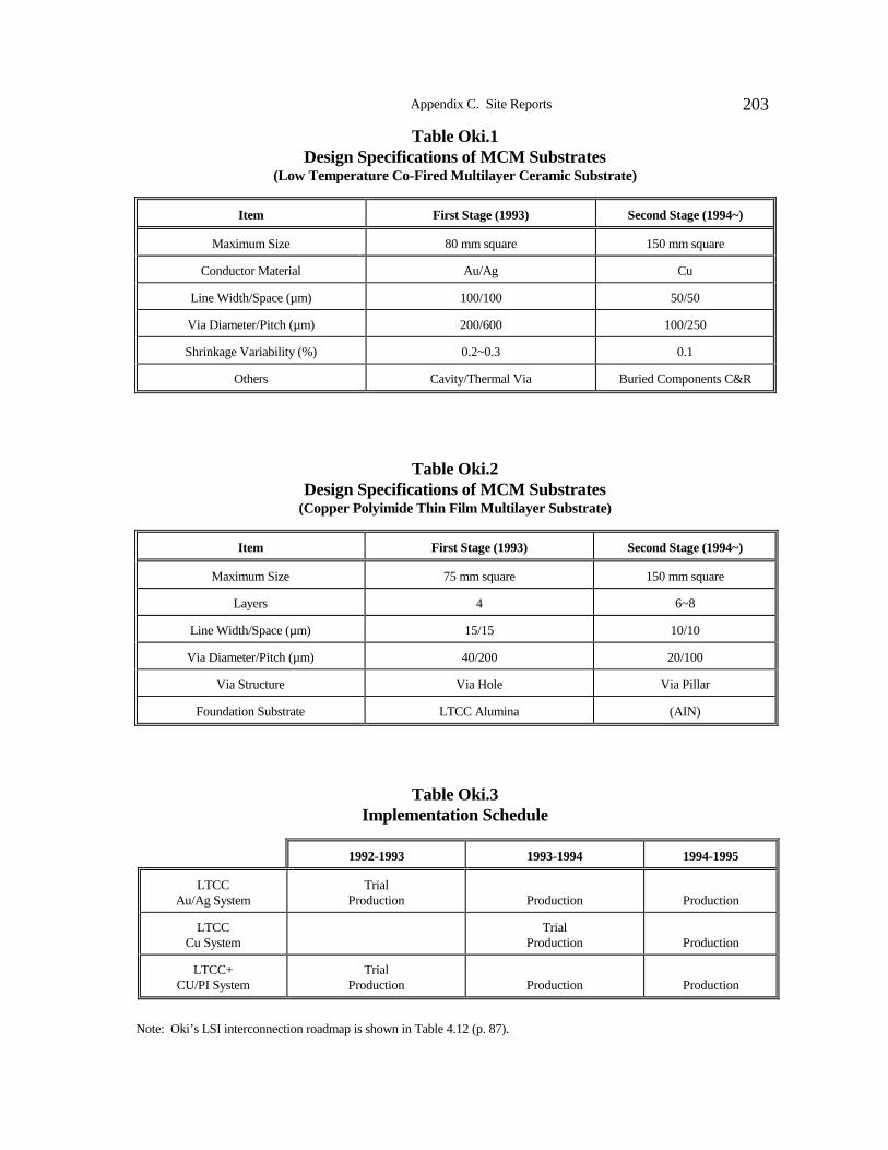
Appendix C. Site Reports 203
Table Oki.1Design Specifications of MCM Substrates
(Low Temperature Co-Fired Multilayer Ceramic Substrate)
Item First Stage (1993) Second Stage (1994~)
Maximum Size 80 mm square 150 mm square
Conductor Material Au/Ag Cu
Line Width/Space (µm) 100/100 50/50
Via Diameter/Pitch (µm) 200/600 100/250
Shrinkage Variability (%) 0.2~0.3 0.1
Others Cavity/Thermal Via Buried Components C&R
Table Oki.2Design Specifications of MCM Substrates
(Copper Polyimide Thin Film Multilayer Substrate)
Item First Stage (1993) Second Stage (1994~)
Maximum Size 75 mm square 150 mm square
Layers 4 6~8
Line Width/Space (µm) 15/15 10/10
Via Diameter/Pitch (µm) 40/200 20/100
Via Structure Via Hole Via Pillar
Foundation Substrate LTCC Alumina (AIN)
Table Oki.3Implementation Schedule
1992-1993 1993-1994 1994-1995
LTCCAu/Ag System
TrialProduction Production Production
LTCCCu System
TrialProduction Production
LTCC+CU/PI System
TrialProduction Production Production
Note: Oki’s LSI interconnection roadmap is shown in Table 4.12 (p. 87).
Appendix C. Site Reports204
Polyimide-Copper Thin-Film Multilayer Substrate
Oki's developments and research in polyimide-copper thin-film multilayer substrate werepresented by Mr. Iguchi, who gave us technical details on the following topics:
• properties of the polyimide resin (thermal, physical and electrical)
• manufacturing process flow of polyimide-copper thin film multilayer substrate (TFML)
• comparison of ground configurations (solid, gridiron, biased gridiron, shifted+bias-gridiron)
• test results for characteristic impedance, propagation delay, transmission loss, cross-talk, and temperature cycling for connection resistance
• planarization process
Oki Development of a Single-PPM Soldering System. Mr. Takei presented Oki's challengesand accomplishments with respect to the goals of CFC elimination and single-PPM soldering.
CFC Elimination. Our hosts reviewed the utilization of CFC materials at the Honjo plant andthe conventional reasons for CFC cleaning of PCBs. The presentation detailed thedevelopment process undertaken to meet the goal of CFC elimination. The process consistedof defining the development target/specifications, defining alternative approaches toeliminate CFCs, the development of experimental fluxes, and testing of the fluxes. Details ofthe reliability test specification, solderability test specification, contact resistance testspecification, and final test results were reviewed. Oki has completed a successfuldevelopment of a flux with RMA reliability, RA solderability, and ease of test pin contact.The Oki Honjo plant manufactured PCBs for 10 months using the new flux without anymajor problems reported, and it eliminated the use of CFCs in March 1992.
Nitrogen Flow Soldering System. The nitrogen flow soldering system required developmentof 3 major subsystems: swing spray fluxer for application of low solid flux; low-consumptionnitrogen and flux fume chamber for management of nitrogen gas and flux fume flow; andcover plate over the solder bath to eliminate micro solder balls. Technical details and testresults were reviewed. Results indicated a failure rate of .02% on a sample size of 21,002PCBs assembled. The smallest component lead pitch on the PCBs tested was 0.5 mm.
Semiaqueous cleaning. The presentation on the development of semi-aqueous cleaningtechnology was given in two parts. Part one discussed the development of alternativesolvents, and part two discussed the development of a cleaning machine.
Solvent development. Mr. Takei defined the basic criteria for selecting an alternative solvent:
• rosin-based solder paste and fluxes can be used
• cleanliness (ionic contamination) is equivalent to CFCs
• chemical residue does not damage PCB reliability

Appendix C. Site Reports 205
• no attack upon the parts and PCBs
• safety (no poison and no flash point)
• low running cost
• no damage such as bubbles to cleaning machine
A detailed matrix for three alternative semiaqueous solvents was reviewed. The reviewcovered the topics of solvent properties, damage to other materials, bubble height andelimination time, and drying ability.
Cleaning Machine Development. There are several basic development criteria for a cleaningmachine:
• 350 mm x 400 mm size PCB to be cleaned
• in-line type and max loading of PCB is 3/min
• no problem for operational reliability- pure water to be used for rinse- lower ionic contamination than CFCs- immersed water of PCB to be dried up
• waste water process to be closed system and low process cost
• lower machine cost than other commercial cleaning machines
Detailed technical matrices were reviewed, covering cleaning methods, waste water process,influence of liquid quantity taken out by passing PCB concentration, cleanliness of PCBs,machine stability, and reliability and quality of post-CFC cleaning methods.
LSI Packing Technology
Mr. Kohara covered the following topics on the subject of LSI packaging technology:
• Logic LSI Packaging- logic LSI package roadmaps- high pin count future direction- wire bond technology improvement- comparison of high-power package cross-sections- thermal resistance- high-speed packages
• Memory LSI Packaging- technology roadmap for memory-SOJ- technology roadmap for memory-TSOP- heat resistance in reflow soldering- concerns of thin plastic package TSOP- package outlines
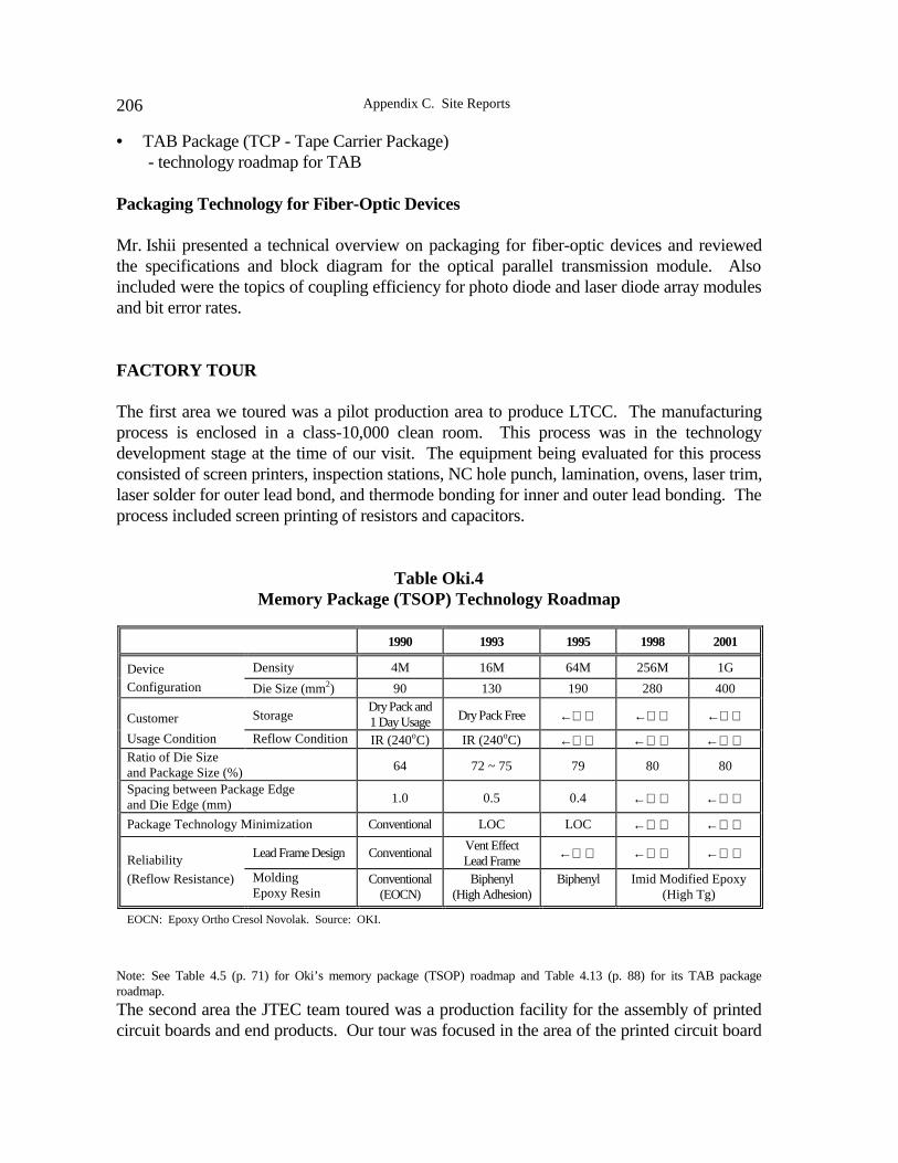
Appendix C. Site Reports206
• TAB Package (TCP - Tape Carrier Package)- technology roadmap for TAB
Packaging Technology for Fiber-Optic Devices
Mr. Ishii presented a technical overview on packaging for fiber-optic devices and reviewedthe specifications and block diagram for the optical parallel transmission module. Alsoincluded were the topics of coupling efficiency for photo diode and laser diode array modulesand bit error rates.
FACTORY TOUR
The first area we toured was a pilot production area to produce LTCC. The manufacturingprocess is enclosed in a class-10,000 clean room. This process was in the technologydevelopment stage at the time of our visit. The equipment being evaluated for this processconsisted of screen printers, inspection stations, NC hole punch, lamination, ovens, laser trim,laser solder for outer lead bond, and thermode bonding for inner and outer lead bonding. Theprocess included screen printing of resistors and capacitors.
Note: See Table 4.5 (p. 71) for Oki’s memory package (TSOP) roadmap and Table 4.13 (p. 88) for its TAB packageroadmap.
The second area the JTEC team toured was a production facility for the assembly of printedcircuit boards and end products. Our tour was focused in the area of the printed circuit board
Table Oki.4Memory Package (TSOP) Technology Roadmap
1990 1993 1995 1998 2001
Device Density 4M 16M 64M 256M 1G
Configuration Die Size (mm2) 90 130 190 280 400
Customer StorageDry Pack and1 Day Usage Dry Pack Free ← ← ←
Usage Condition Reflow Condition IR (240oC) IR (240oC) ← ← ←Ratio of Die Sizeand Package Size (%) 64 72 ~ 75 79 80 80
Spacing between Package Edgeand Die Edge (mm) 1.0 0.5 0.4 ← ←
Package Technology Minimization Conventional LOC LOC ← ←
Reliability Lead Frame Design ConventionalVent EffectLead Frame ← ← ←
(Reflow Resistance) MoldingEpoxy Resin
Conventional(EOCN)
Biphenyl(High Adhesion)
Biphenyl Imid Modified Epoxy(High Tg)
EOCN: Epoxy Ortho Cresol Novolak. Source: OKI.
Appendix C. Site Reports 207
assembly. The manufacturing facility was organized into islands of automation; theirmanufacturing operations are controlled by a central host computer. The operation beginswith an automated storage and retrieval system. The management information system (MIS)defines whether or not incoming material, received from a vendor, requires inspection beforebeing placed into the storage area. Components are automatically identified and retrieved bythe use of computer control in combination with a bar code system. An automated guidedvehicle is used to deliver material to the process lines; this includes magazines of printedcircuit boards and prekited component feeders for the placement machines. The standardscreen, place, and reflow manufacturing process is being used for surface mount assembly.Bar code labels are applied to bare printed circuit boards, and automated in-line inspection isperformed immediately after screen printing of solder paste, component placement, andsolder reflow. Automated inspection and test of individual components is performed withinthe placement machines. Solder reflow profiles are downloaded from the host system.Presently Oki is using vision for solder reflow inspection but is developing a 3-D laserinspection station. A warp prevention robot was developed for processing of large printedcircuit boards through the reflow oven. Design rules have been established to obtainoptimum yields within the manufacturing process. The rules define the placement location ofcomponents onto the printed circuit boards
SUMMARY
Oki is organized into three business divisions that are highly integrated. The companypossesses the technological capabilities required for success in the coming multimedia age.The organization is involved in development and production of products, systems, materials,automated equipment, and manufacturing processes. Oki gives credit to automation as thekey in obtaining product yield improvement with high quality and reliability. The drivingforces for its development of new products are cost, weight, and miniaturization.
During the JTEC visit our hosts were open in technical discussions and extremely hospitable.
Appendix C. Site Reports208
Site: Sony Corporation6-7-35, KitashinagawaShinagawa-kuTokyo 141, Japan
Date Visited: October 4 and 5, 1993
Report Author: N. Naclerio
ATTENDEES
JTEC:
P. BarelaW. BoultonN. Naclerio
HOSTS:
Yoshiyuki Kaneda Senior Managing DirectorYoshiyuki Yamada Member, Board of Directors, Dir. of Research CenterTakehisa Okada Senior General Manager, FA and Precision ProductsJunzo Wachi Deputy Senior General Manager, Marketing, FA and
Precision ProductsYunosuke Hayakawa General Manager, Production Technology Coordination
Div. Production Technology Development Systems Engineering Div., FA
Yoshiko Numata Government and External Relations Div., Trade and External Relations Group
Koichi Motegi Manager, Government & External Relations Div., Trade & External Relations Group
BACKGROUND
Sony Corporation has $34.4 billion in worldwide sales, of which $10.5 billion is in the U.S.,$8.9 billion is in Japan, $9 billion is in Europe, and $6 billion is in Asia and other areas. Sonyhas 126,000 employees with 35 manufacturing plants in Japan, 13 in North America, 14 inAsia, and 14 in Europe. The company is organized around business sectors including audioproducts (audio components, general audio, automotive, and personal communications);video products (personal video, home video); television; personal information systems; andbusiness and professional products. Our host, Mr. Kaneda, was responsible for componenttechnologies (including semiconductors, electronic devices, batteries, and recording media)and factory automation.
Appendix C. Site Reports 209
Mr. Kaneda described the borderless, global marketplace in which Sony competes for newand existing markets. He stated that in addition to building creative products, it is necessaryto develop production innovations and equipment for advanced assembly and ultraprecisionin order to maximize the company’s value added and profits.
SONY’S COMPETITIVE STRATEGY
Precision Manufacturing And Concurrent Engineering
Mr. Hayakawa stressed the importance of precision manufacturing and concurrentengineering in order to produce compact, lightweight, and highly reliable products. As anexample, for the TR5 camcorder (introduced in 1989), product planning began with a visionof a video recorder that would fit in the palm of one hand. This fixed the external dimensionsof the recorder and drove the size of the circuit board and recording head. Development workbegan concurrently at the design divisions for issues of high-density component packages,assembly, PCB, IC, tape transport mechanism, recording cylinder and head, lens, and high-density recording tape. Simultaneously, development began in the respective productiontechnology organizations.
In the area of printed circuit board technology, the product requirements meant the use of thevery latest surface mount technology. Subsequent versions of the TR5 reduced the PCB sizeby 75%. In order to achieve 100 µm solder lands with 100 µm spaces, Sony developed a lowmelting point solder with more uniformly shaped and sized solder particles and a new metalscreen technology for more uniform printing. The TR1 camcorder introduced in 1992achieves 20 components/cm2, or about twice the component density of the TR5. Sony feelsthat future products will require 30 components/cm2. Discrete surface mount components assmall as 1.0 mm by 0.5 mm are currently being used. Surface mount technology is also usedin Sony’s larger products because it is less costly, higher performance, and can bemanufactured with higher quality and reliability than through-hole technology.
Another example of the need for precision manufacturing in the camcorder is in the recordinghead. In the manufacture of the very narrow head with 0.3 µm head gap, it was necessary to cutferrite material to a thickness of 2 µm and a height of 110 µm. This required the developmentof a spindle to precisely control a diamond blade. The head is wound 55 times with 30 µm wirethat must pass through small slots in the head. This required the development of a precisionwinding machine. The development of these machine tools proceeded concurrently with thedesign of the product which could not have been built with production equipment available inthe marketplace. Therefore, according to Mr. Hayakawa, "manufacturing of the requiredproduction equipment must be done in-house. This has become a truly creative activity becauseit makes the manufacturing of creative products possible."
Sony has turned its expertise in factory automation into a new product area. Sony sells mostof the equipment it develops to outside customers. We toured the FA demonstration center

Appendix C. Site Reports210
and surface mount (SMT) assembly training center where customers come to learn how tooperate an SMT line. Sony's FA group has grown to about $500 million a year in revenue,with 80% of that still coming from internal Sony customers.
Materials And Process Technology
Also cited as important were materials and process expertise. As an example, the design ofthe compact disk player was cited. The heart of a compact disk player is the optical pickuphead. In designing the head, Sony considered alternative methods of precision assembly withregards to suitability for automation, reliability, and contribution to size, weight, and costreduction. Adhesive bonding was the best method for size, weight, and cost reduction, butwas poor in the areas of reliability and automation. Because it offered significant productadvantages, Sony decided to focus on improving the productivity of the bonding technique.Key parameters to optimize were surface preparation, bonding agent, and process controltechnique. Sony developed a light ray cleaning method to improve surface wetability andselected nine different bonding agents for joining various components in the pickup head.Sony now manufactures 60% of all the world’s optical pickup assemblies.
Added Value and the Importance of Manufacturing Key Components
Mr. Hayakawa stressed the importance of manufacturing key components of a product fromthe viewpoint of value added. In the case of a compact disk player manufactured by Sony,only 10% of the value added comes from assembly. In contrast, the key devices (opticalpickup, semiconductors, lenses, motors, transformers, and PCBs) account for 55% of the totalproduct cost. Similarly in the case of the 8 mm camcorder, assembly is about 12% of theadded value, and key devices (CCD, ICs, drum, PCB, magnetic head, motor, lenses,viewfinder, and sensors) make up about 60%. Sony manufactures about 60% of the keydevices for the compact disk player and about 45% of the key devices for the 8 mmcamcorder, and it intends to increase both percentages in order to increase profitability.
In the case of the Video Walkman, Sony's palm-sized TV/VCR, Sony procures the displayfrom an "associate" company. According to Mr. Kaneda, the miniaturization technology forthe electronics and tape transport mechanism was more important than the display technologyin realizing the products. The only flat panel displays manufactured by Sony are for use incamcorder viewfinders. Sony feels that LCD technology is only applicable to moderate-sizeddisplays and that its Trinitron CRT technology is superior for wide-screen, high-definitionapplications.
Effectiveness of Automation
In addition to processes that require automation in order to achieve precision that cannot beachieved with human hands, Sony cites several other benefits from its use of automation.These include reductions in factory start-up time, in manufacturing defects, and in manpowerrequirements.

Appendix C. Site Reports 211
In the case of the optical pickup head for the compact disk player, early manufacturinginvolved manual assembly and adjustment by highly skilled technicians. Worker traininglimited Sony’s ability to ramp production and expand overseas. Automation of the line tooka lot of preparation, but was accomplished in four months. Replicated lines in Singapore andFrance took only two to three weeks to bring up to speed. The operators got one month oftraining in the Japanese factory prior to startup of the overseas plants.
In the case of color television production, robots were introduced to replace 99% of themanual parts insertion. In addition to the reduction in labor costs, the defect ratio wasreduced by 90%, the PCB rework rate was reduced by 75%, and the increased productuniformity allowed Sony to greatly simplify final product adjustments.
In the case of the Walkman a completely automated assembly and adjustment system wasinstalled. Defect levels during initial manual assembly were 0.2% in the first week and 0.1%in three months. However, during the first week of automated assembly, the defect ratedropped to a steady 20 PPM. The introduction of subsequent Walkman models into the samefactory required additional investments of 9.1%, 3.5%, and 1.5%, respectively, for theproduct changeovers. In addition, the time to bring up the new systems dropped from sixweeks to five weeks, then to three weeks, and finally to one week.
As a result of Sony's skills in automation, coupled with its focus on design formanufacturability, it was able to increase sales by 121% between 1987 and 1990 with only a35% increase in the number of direct operating employees. Manufacturing processes are firstestablished and streamlined in terms of manpower, equipment, and materials, then the finalsystem is automated. Because of the heavy use of automation, an increasing fraction of theoperators at Sony are involved in maintenance and indirect operations. Sony employs over1000 people in its factory automation and precision products group and 300 in productiontechnology within Mr. Kaneda's organization.
Quality and Reliability
According to Mr. Kaneda, any product introduced into the marketplace must have highquality and reliability. Sony tries to reuse well characterized components from previousproducts in order to achieve high quality in newly introduced products. As much as possible,basic failure mechanisms are identified in the prototyping stages. Once failure mechanismsare understood, stress tests can be designed using heat, environment, or time.
Product Lifecycles
Product lifecycles are determined by market conditions. On average, minor product changesoccur about once a year. However, in the case of the Sony Walkman, new models areintroduced every six months or less. Major model changes that require the introduction ofnew technology occur only once every three to five years. Sony is working to prolong theproduct's life in the marketplace.
Appendix C. Site Reports212
Advanced Packaging Technology
Sony has a 3 dB theory. That means that the next generation of any product should cost halfas much and be one-third the size and weight. In order to reduce the size of the nextgeneration of products by 30%, multichip module technology will be required. At the time ofthe JTEC visit, Sony was not using MCMs in any products because they were too expensive.However, Sony was planning to develop the equipment and processes necessary tomanufacture them more cheaply.
Product Design
A standard design system is used within Sony. The company does not enforce this onexternal suppliers; they can maintain their independent design styles. Internal and externalsuppliers are both generally part of the product team from very early in the product life cycle.External suppliers are expected to make investments in new production technology. FApeople are always an integral part of the product team. Product design includes reducing thenumber of components and standardizing components as well as manufacturing methods.Design for assembly difficulty is measured by design and production engineers using astandardized methodology. Design for assembly software was in use at the time of the JTECvisit, and design for disassembly software was expected to be available within one year. Thefocus on disassembly is driven by end-use markets such as Germany where some stringentrequirements are already being discussed. Full 3-D modeling is available for design ofproducts.
SONY RESEARCH CENTER, YOKOHAMA (10/4/93)
Sony invests about $2 billion per year in R&D, two-thirds of which is product development.It has four corporate laboratories and nine development groups located within the productgroups. Sony maintains R&D labs around the world. In the United States, there are twomajor technology centers — one in San Jose, CA, and one in Montvale, NJ — and severalsmall laboratories, some of which are collocated with manufacturing operations. Theresearch center in Yokohama consists of five departments: Semiconductors, Materials,Materials Characterization, Computational Materials Science, and Seeds Laboratories. TheSeeds Laboratories focus on specific new materials or devices. The center has recentlydeveloped a blue laser diode for optical recording, new materials and devices for magneticrecording, and lithium ion batteries
As technologies mature, they are transferred to manufacturing organizations. For example,CCD imaging was a top priority in the early seventies. Once the first CCD camera wasdemonstrated, the group was transferred to a semiconductor production site to begindesigning the pilot and production lines. Battery technology, MOCVD GaAs, and magneticrecording-related technologies have also been spun out to product groups, as was the plan forthe blue laser diode in the near future. The main vehicle for technology transfer seems to be

Appendix C. Site Reports 213
the movement of people. Researchers generally come to the research center directly fromuniversities. After working at the research center for a number of years they go out to theproduct groups and remain there so that they can develop and modify the technology in thefield of their expertise. From there, they go on to implement the technology inmanufacturing. As a result, very few of these people return to the Research Center.
Most R&D is "needs"-oriented. Product ideas evaluated and selected by top management, attimes by the chairman himself, necessitate specific technology development. For example,the palm-sized camcorder required a small sized CCD, a small lens, a high-density printedcircuit board, and other key technologies. By specifying timetables and clear targets, R&Dfunds are allocated to those areas requiring the most acceleration. Currently, 20-30% of thecenter's R&D is funded by the product groups, and the corporation is trying to increase thatamount to 50%. One engineer in every research group is assigned the responsibility formarketing the technology to the product groups. In addition, annual technology fairs are heldto showcase ongoing R&D products to the product groups. A new corporate "developmentlaboratory" has been established to further develop new products that might not fit into anyexisting product group.
We did not see any advanced packaging R&D being conducted at the Research Center. MCMdevelopment is reportedly underway within the semiconductor division and within theProduction Technology Development Group's High-Density Mount Laboratory located inTokyo. Sony Chemical, a subsidiary, is reportedly doing advanced PWB research.
One complex new piece of materials analysis equipment was being operated by an Americanwho recently earned a Ph.D. at a leading U.S. research institution. He said that he came tothe research center because it was the best equipped in the world for the work that he wantedto do.
SONY’S KOHDA FACTORY (10/5/93)
O. Uchida - PresidentT. Kono - Senior Executive DirectorH. Yamada - Engineering and Design
The plant was established in 1972 and currently designs and manufactures Sony's advanced8 mm camcorder products. Products include 8 mm camcorders and tape decks and keycomponents such as tape drums, tape transport mechanisms, and reference tape. The keycomponents manufactured at Kohda are primarily exported to overseas Sony assembly plants.The plant also manufactures some low-volume products such as editors, special effectsgenerators, and color printers. The plant employs 2,040 people including 200 engineers, halfof whom are production engineers. The plant has a capacity to produce 550,000 recordingdrums and 250,000 camcorders per month. Overseas plants primarily do final assembly andmanufacture some commodity products like standard quality recording tape.

Appendix C. Site Reports214
The tape drum, transport mechanism, and PCB are key components of the camcorder becausethey determine the picture quality, reliability, and intelligence of the unit, respectively. Otherkey components such as the CCD, LCD viewfinder, and ICs are manufactured at other Sonyplants. The most advanced production technologies are employed including precisionprocessing, automated assembly, high-density surface mounting, and automatic picturequality adjustment. The plant was ISO 9002 certificated at the time of the JTEC visit; itreceived ISO 9001 certification in November 1993.
The majority of the operation is automated with Sony FA and precision assembly equipment.According to Sony, the level of automation for various tasks are: 98% for SMD placement,100% for drum manufacture, 98% for standard tape deck assembly, 71% for compact tapedeck assembly, 100% for CCD assembly, and 75% for camera adjustment. The lower levelof automation for the most compact tape deck is due to the need for lots of adjustments.Much of the final product assembly that does not require much precision is done manually.Two exceptions are video adjustment and system testing, which is fully automated using avery impressive system.
The SMT factory we visited was producing PCBs for the TR1 camcorder. Each cardcontains approximately 1400 components. The primary bottleneck in the plant is the flow ofmaterials to the assembly machines, which have to handle up to 100 part types. The CIMsystem identifies which placement machines are going to run out of parts and notifies anoperator approximately 30 minutes in advance. When operators reload the machines, barcode readers verify that the correct parts have been loaded. Only one PWB type at a time ismanufactured on any one SMT line. Minor product changeovers take about 15 minutes, but amajor product changeover could take two to four hours. Machine instructions aredownloaded from a factory CIM system. It appeared that the majority of the SMT assemblytime was consumed with the placement of small discrete devices. The engineering managersaid that the company was looking at new methods of feeding the components to theplacement head that would cut placement time and also looking at the use of thick-filmhybrids with integral passive components for higher frequency applications such as HDTV.
The tape drum factory we visited is completely automated and produces the complete tapedrum starting from bars of aluminum. The material handling system for the partiallymanufactured drums resembles vacuum cleaner hoses draped from station to station throughwhich the tape heads roll. During the final assembly steps the recording head must bepositioned in a groove in the cylinder with ∀1 µm accuracy. In order to achieve this, a visionsystem inspects each drum and measures certain critical dimensions. One of perhaps 100spacers is placed between the drum and the head that will result in ∀5 µm placementaccuracy of the recording head. The screw that holds the head in place is then tightenedunder computer control to achieve the final ∀1 µm accuracy. This simple but elegantsolution presumably achieves the necessary accuracy without the expense of machining everyhead to the final dimensional accuracy. It should be noted that the final assembly step justdescribed, as well as several of the other manufacturing steps, are accomplished usingspecialized machines built by Sony.
Appendix C. Site Reports 215
The assembly of the tape decks is accomplished with over 100 Sony precision assemblyrobots organized into 6-8 parallel production lines. During the time that JTEC panelists weretouring the plant we saw a couple of events where a yellow light alerted an operator to comeand assist with some operation. Generally, the operator spent no more than a minute or twobefore he had the machine back in operation. It appeared that there was approximately oneoperator per dozen robots in the plant. Our hosts told us that when a robot failure cannot befixed quickly a new robot may have to be brought in to replace it. During the time aproduction line is down, all but a few high-precision operations can be replaced by humanoperators. Failures that take a robot down for an entire shift happen about once every sixmonths.
In the final assembly operation, the tape deck, camera, and PCB are brought together. Oncethe major subassemblies have been brought together, the camcorders are powered up andfocused on a series of images. A fully automated system makes 6-8 adjustments to thepicture quality of each camcorder and burns the settings into an onboard PROM. Partiallythrough the process, a robot inserts a tape into the camcorder and tests the record andplayback functions. The fully tested and adjusted camcorders then proceed down anassembly line to a series of stations where operators manually perform the final assemblysteps including the attachment of flex wiring circuits to the external case. This line producesapproximately 1,200 camcorders per shift.
Product and production design for the 8 mm camcorder products is also located at the Kohdaplant. The design center is located in the upper stories of the factory building directly overthe production floor. The engineers work in a open space with lots of paper drawings andactual hardware lying around. A glass-walled room contains a mainframe computer and anumber of workstations. At the time of the JTEC visit, CADAM, a 2-D mechanical CADpackage was in use for the design of the robots and the mechanical assemblies. It isinteresting to note that these two operations were going on at adjacent workstations, a sightnot likely to be seen in the United States. The engineers rely on the reuse of commoncomponents across and within product lines to shorten development time. For example, Sonymanufactures a family of tape transport mechanisms that are used in both its camcorders andits Watchman.
SUMMARY
Sony is a best-of-breed worldwide consumer electronics company. Its leadership appears tobe based on a combination of innovative products, precision manufacturing skills, andcontinuous improvement. Our hosts credit Sony’s leadership in the manufacture of high-quality, low-cost electromechanical products to its leadership in precision assemblyequipment, materials and processes, and factory automation. From what we saw, it certainlyappears to be a leader in precision assembly. That leadership is further demonstrated by itsability to market its precision assembly and FA systems to other manufacturers. Sony’s focuson in-house production and integration of factory equipment seemed fairly consistent with
Appendix C. Site Reports216
other companies we visited in Japan, but in stark contrast with the direction of leading U.S.electronics companies. While Sony’s investments seem justified in areas such as machiningthe recording head or assembly of the tape transport mechanisms, where the company hassucceeded in producing unique and competitive equipment, its investments seem lessjustified in areas such as surface mount assembly, where numerous companies producecomparable equipment.
According to Sony representatives, "creativity" has always been an important concept atSony, one of the leaders in introducing new and innovative products to the market. In orderto manufacture those products, Sony has been developing new equipment, and that is whereits strength lies. It also has a flexible policy that promotes the effective use of existingmanufacturing equipment available in the open market.
Like Sony’s competency in factory equipment, its strong competencies in materials andprocessing appear to be a competitive differentiator in the marketplace. Examples like thedevelopment of solder paste for very-fine-pitch component assembly, or the exploitation ofadhesive bonding for the compact disk optical pickup, seem to demonstrate the value of itsprocess. Few if any U.S. electronics firms have comparable depth in the materials arena.
Sony also recognizes the importance of controlling the manufacturing of its criticalcomponents. However, according to Sony representatives, it is not Sony's policy toconcentrate manufacturing of key components in Japan. In fact, its corporate policy promoteslocal manufacturing. This concept is valid for key components as well as products, and thusSony has many key components plants located within the region of product manufacturingplants on a worldwide basis.
Sony, like other Japanese companies the JTEC team visited, seems almost obsessed with theuse of automation to increase productivity and quality. The only tasks being done by humanswere those that did not require much precision or perhaps were too expensive to automate,such as the final assembly of the camcorder case.
Our hosts seem to recognize the importance of electronic packaging as a competitivedifferentiator. They listed the PCB as a key component of both the camcorder and thecompact disk player. Sony seems to be pushing surface mount assembly to its limits throughincremental refinements rather than any revolutionary technology. Based on ourobservations, one of the biggest drivers for a change in packaging technology at Sony isreducing the number of discrete components needing assembly on PWBs. While digitizationof the electronics and increased IC integration will certainly help, a substrate technology withintegral passive components would drastically reduce part count and provide a significantarea savings.

Appendix C. Site Reports 217
Site: TDK Corporation13-1, Nihonbashi, 1-chome, Chuo-kuTokyo 103, Japan
Date Visited: October 7, 1993
Report Author: G. Meieran
ATTENDEES
JTEC:
W. BoultonG. HarmanG. MeieranR. Shelton
HOSTS:
Fumio Uchikoba Researcher, Materials Research Center, NaritaKenichi Aoshima Manager, Corporate Planning OfficeNoboru Yamaki Dept. Director, General Affairs, NaritaAkira Okamoto Manager, Advanced Products Development Ctr.Mitsunobu Goto Manager, Corp. Research and Development Dept.Akira Fukuno Senior Researcher, Materials Research Ctr.Tadashi Mitsui Chief Engineer, Ferrite DivisionKouichi Yajima Manager, Materials Development Section,
Corporate R&DTakashi Horiuchi Manager, Production Engineering Dept.Tatsushiro Ochiai Executive Director, General Manager, Materials
Research Ctr.
BACKGROUND
The visit to TDK was bimodal; a very interesting and useful morning in which we discussedthe TDK packaging and assembly issues, and an afternoon plant tour of the ferritemanufacturing facility in Narita, which was interesting but not particularly pertinent to thepackaging and assembly issues. Hence, this site report concentrates only on the morningsession, and only mentions two aspects of the afternoon tour that had some pertinence topackaging and assembly. Most of the information discussed below was presented to thevisiting JTEC team in the form of two interesting and extremely well-done video tapes; wedid not personally see any of the processes or equipment described in these tapes.
Appendix C. Site Reports218
TDK appears to be a very well run company with excellent facilities, top quality people, andexcellent technology. It was formed in 1935 by the invention (so we are told) of ferrites. Itappears to be a world leader and the world's largest supplier of ferrites, ferroelectrics, andother electronic materials. Its products are used everywhere, such as in floppy and hard disks.As a result of this path, TDK has become very adept at manufacturing passive and activeelectronic components, and in their assembly into high-quality PC boards. Indeed itsmanufacturing capabilities in the component area are no less than phenomenal; TDKproduces very small parts in huge quantities, using state-of-the-art equipment and processingcapabilities. Because there is a need to have equipment available to assemble these smallcomponents, TDK makes much of its own equipment, and, as other Japanese companiesshowed us, it is prepared to sell its assembly equipment to the external market (except for itslatest state-of-the-art manufacturing equipment).
The quality of TDK products appears to be very high; design of products and processes isthorough and well done. Video tapes describing all this were among the best I have seen andwere convincing. Even at the fairly old ferrite plant, most of the processes are automated; itappears as if yield is good and quality levels are high. However, we had the impression fromthe ferrite plant visit that TDK is not addressing other manufacturing issues; there was lots ofinspection, lots of inventory, and little evidence of motivation to do anything differently.
Since much of TDK’s product line consists of old products with very little profit margin, it ismoving some of its manufacturing overseas, to China and Malaysia, and has challenged itsdomestic staff to come up with new, high-value-added products. It will use its currentproducts, but will look to incorporate these into high-value products. In newer lines, such asseen on the video tape, there is little evidence of inspection, and automation appears to be100%. It was impossible to see what inventory levels were present. The TDK philosophyseems to be, "Good enough is good enough." If something requires automation or specialmanufacturing processes, fine, the company will develop and provide technology andautomation as necessary; otherwise, incremental improvement is satisfactory.
TDK has about 25,000 employees total, about 7,000 of whom are domestic. About 60% ofits manufacturing capability was in Japan at the time of the JTEC visit. Its product lineincludes ferrites, semiconductors, ceramic components, recording media, metallic products,and a variety of other mostly electronic products.
All that we saw was consistent with TDK’s stated company philosophy, "RespectingOriginality," with its company motto, "Contribute to Culture and Industry ThroughCreativity," and with its employee attributes, "Vision, Courage, Reliance."
COMPONENT DESIGN AND MANUFACTURING
TDK designs and fabricates components such as small transformers, inductors, and capacitorsin huge (hundreds of millions of individual pieces) quantities. It also makes hybrids,

Appendix C. Site Reports 219
sometimes incorporating passive elements in an active circuit. Consequently, it manufacturesa very broad line of products. Indeed, its product line numbers in the range of 140,000,although it is trying to reduce this to a more manageable level (30,000?). TDK clearlyappears to be competitive with the state of the art, or is setting the standards for state of theart, in the fields in which it competes.
The sizes of the small parts TDK manufactures is staggering, even to those of us in thesemiconductor industry, in which "small" refers to line geometry, but the chips may be fairlylarge. Its smallest capacitors are, for example, smaller than a grain of pepper (one sneeze and400,000 parts disappear!). Even these tiny objects are made up of many layers of alternatingdielectric and metalization, cleverly laid down in sequential sides of a chip to give a rampedstaircase effect, in the case of physically small inductors.
The emphasis is on cost and size reduction. TDK seems less interested in integration; indeedit seems to be the opposite of a company such as Intel, which makes individual chips thatintegrate many functions and grow larger as a result of integration; TDK wants to makethings as individual components and as small and inexpensive as possible. As a result, it hasdeveloped a line of assembly equipment that can handle its small and exceedingly wide lineof products. This line of equipment is extremely sophisticated, very precise, and totallyautomates assembly of PC boards; operators can barely see, much less manually handle,TDK’s line of small components. The company’s equipment appears to be a decade ahead ofanything comparable in the United States.
Customer Focus
TDK might be expected to be a leader in high-temperature superconductors, resulting from itsextensive expertise in ferroelectric device technology. But a technical as well as businessperspective arose when superconductors were discussed during the JTEC visit. On the onehand, TDK spent several years and lots of money looking at high-temperaturesuperconductors; however, there were several technical problems that suggested that it neednot bother, and work on these materials has ceased. Even more important, our hosts statedthat even if all the technical problems were solved (materials synthesis, defects, hysterisis,whatever), the devices would still need to be operated below room temperature, so TDKwould likely not get involved. The customer base would not be expected to want to usecooled packages, and since TDK makes products for its customers, it is not likely to getreinvolved. In this sense, TDK looks at technology to help develop markets, but, clearly themarket rules, not the technology.
TDK’s ceramic substrates are quite thin, say ~5 µm, and it has solved the cracking problemsnormally associated with such thin brittle layers. It then builds up 70 or 100 layers, makingthese small, 1 pf capacitors. It has solved cracking problems by carefully selectingmetalization materials (e.g., nickel), closely matching the thermal expansion coefficients ofthe materials, and firing at relatively low temperatures.
Appendix C. Site Reports220
Assembly Automation Equipment
Initially, equipment was developed in-house to handle only TDK products, under theassumption that the company could get a better lock on the market this way. People whobought their equipment to assemble some TDK products would find that they could only useit on TDK product lines. This strategy back-fired. It was too focused on TDK product lines,and the competition from companies such as Matsushita, which offered a more "openarchitecture," caused management to change this strategy. Their present line of equipment,made by a company called Avimount, accounts for 7% of TDK's business.
Cost Basis
TDK has calculated that labor costs in Japan are on the order of two seconds per yen. Since amultilayer capacitor costs about one yen, it is impossible to inspect products. Hence, TDKhas adopted the philosophy of zero defects. Indeed, current figures show a defect rate on thelevel of 1 to 10 PPB. On assembled products, there is a defect level of 10 to 100 PPM.Clearly, TDK drives all non-value-added costs out of the manufacturing process; U.S.companies might invest in inspection and testing, while TDK invests in process improvement.
TDK is ISO certified, but only because of U.S. customers. There appears to be no great drivein Japan for standards as there are in the United States.
Technology
Our hosts showed us an interesting expert system, of which they seemed quite proud. This isa system that designs products by having a customer choose magnetic properties, and theexpert system provides the details of how to make the product, e.g., composition, firingconditions, etc. Or the customer can choose a composition for the three-dimensional phasediagram, and the magnetic properties and appropriate processing conditions pop out. This isa neat piece of software, with some excellent graphics, and it appears to be in use.
TDK has an interesting way of making rare-earth iron magnets. It fires (sinters) magneticbodies made from fine powders with intentionally lower oxygen content in order to get rid ofnonmagnetic rare earth oxide impurities. It has introduced an hydrogen absorption anddesorption process to ingots so that the ingots become brittle. Since brittle ingots need lessimpact for fine pulverization, they can prepare fine powder by applying lower oxygen content— a neat way to use a failure mechanism to help solve a problem and simplify a process.
The JTEC team got some idea of the persistence of Japanese companies in pursuingworthwhile ideas and technology, and the inverse, the rapid discarding of even good ideasthat do not fit their marketing molds. At Narita, we saw a (new then) green tape line formetalized ceramics that TDK had been pursuing for seven years and was only then beingreadied for mass production. This line is for glass-ceramic composites, with a low (~900oC)firing temperature. The material is low-cost and strong, but does not have the thermal

Appendix C. Site Reports 221
conductance of pure ceramics such as alumina. But TDK sees a market and is going to startproliferating the technology in the near future.
This is to be contrasted with the rapid elimination of the high-Tc superconductor program,which simply did not meet TDK’s customer profile, even though it seems to have totallyappropriate technology and expertise, and the technology seems to have promise for somemarkets.
Indeed, this seems to be an area of some contention; how does a company like TDK takeadvantage of new opportunities? TDK is excellent in technology, but seems to be less strongin developing new markets that may be a bit out of the path of its existing markets.
SUMMARY
The impressive features about TDK are its technology for mass producing a large variety ofvery small, high-quality products. As a consequence, it has developed a very strong customerconsciousness and a wealth of supporting tools (such as assembly equipment for mountingthese small parts). It has a strong company focus on producing quality products that requireminimal inspection, on satisfying the customer with the range of products it produces, onmaintaining a product line compatible with its technological expertise, and on persisting untilthe technology problems associated with its product lines are resolved.
Any new products must meet the above criteria. As a result, TDK is a very strong force inJapanese electronics manufacturing and has an impressive track record ranging frominnovation and invention (of ferrites) to implementation and marketing. Its electronicproducts line is broad as well as deep, and is state-of-the-art. Whether or not TDK will be asstrong a force in marketing assembly equipment remains to be seen, but there is little doubt itis capable of strongly entering this market.

222
APPENDIX D. SPONSORS OF THE JTEC STUDY ON ELECTRONIC PACKAGING IN JAPAN
National Science Foundation
Paul HererLinton Salmon
Advanced Research Projects Agency
Lance GlasserNick Naclerio
National Aeronautics and Space Administration
John EvansJillian EvansPhil Barela
Department of Commerce
Phyllis Genther-YoshidaTom KusudaGeorge Harman
223
APPENDIX E. ATTENDEES AT THE INDUSTRIAL REPRESENTATIVES MEETING ON APRIL 19, 1993
Lisa Anklewich FordW.R. Boulton Auburn UniversityMung Chen IntelGerry Dillman IBMJohn L. Evans ChryslerEdward Hakim Army Research LabGeorge Harman NISTJeffrey Hawthorne MotorolaKim Hyland AppleRichard Jaeger Alabama Microelectronics S&T CenterMike Kelly Georgia TechBruce Kramer NSFJohn Kukowski Rochester Institute of TechnologyJudee Mussehl-Aziz International Trade AdministrationNick Naclerio ARPALuu Nguyen National SemiconductorDon Orr MCCMike Pecht University of MarylandJohn Peeples NCRGordon Roberts AT&TLinton Salmon NSFMike Snyder UniversalMelissa Timmons Hayes Microcomputer ProductsNicholas Vadala Digital Equipment CompanyE. Jan Vardaman TechSearch InternationalDaniel Ward Delco ElectronicNancy Watts Hayes Microcomputer Products

224
APPENDIX F. GLOSSARY
ACA Anisotropic Adhesive Connection
AD Active Device
AGV Automated Guided Vehicle
AI Artificial Intelligence
AMLCD Active Matrix Liquid Crystal Display
ASIC Application-Specific Integrated Circuit
ASIM Application-Specific Integrated Module
AV Audiovisual
AXPC A UNIX operating system unique to Japan
B-PGA Bumped Pin Grid Array
BGA Ball Grid Array
CD Compact Disk
CD-ROM Compact Disk Read Only Memory
C-PGA Ceramic Pin Grid Array
CCL Copper Clad Laminate
CFC Chlorofluorocarbon
CAD Computer-Assisted Design
CAE Computer-Assisted Engineering
CAM Computer-Assisted Manufacturing
CIM Computer-Integrated Manufacturing
CISC Complex Instruction Set Chip
COB Chip On Board
COF Chip on Flex Board
CTE Coefficient of Thermal Expansion
CRT Cathode-Ray Tube
DCC Digital Compact Cassette
DFX Design For Excellence
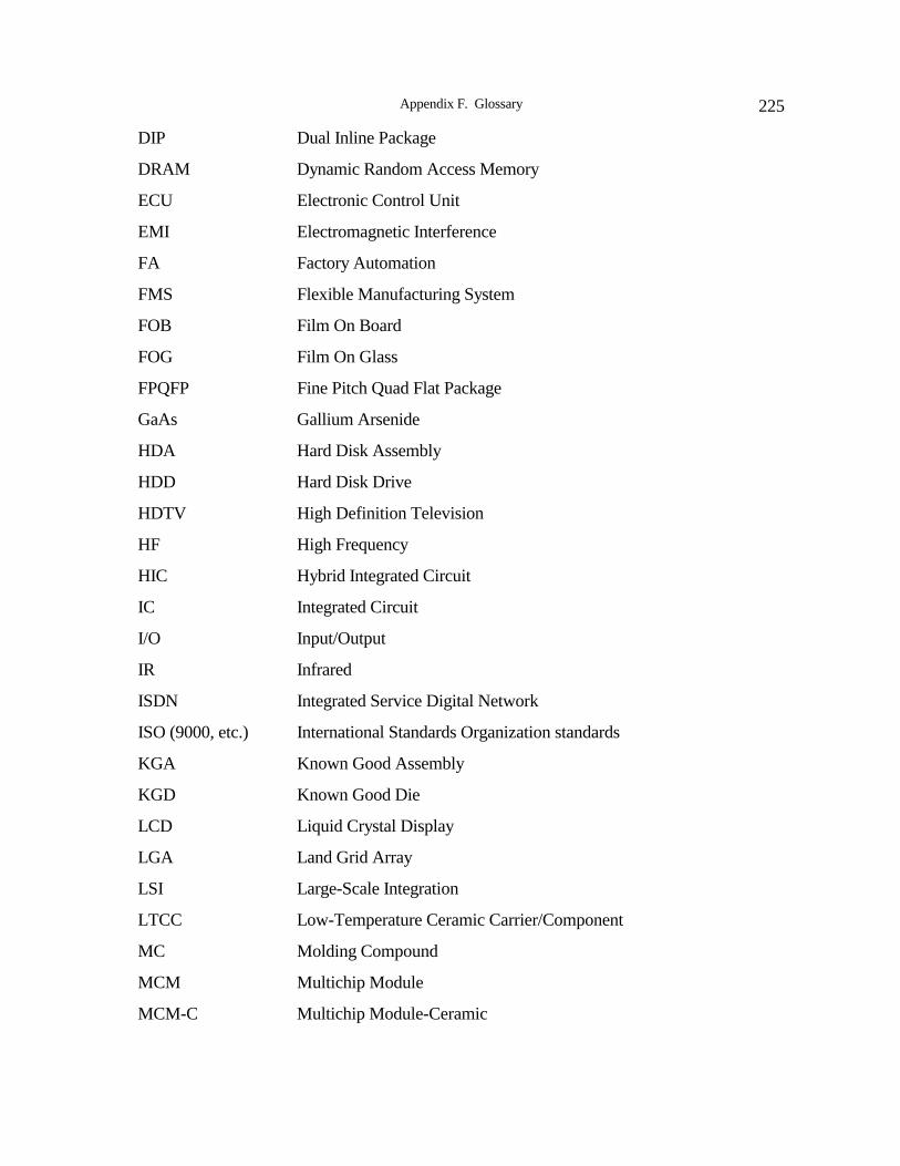
Appendix F. Glossary 225
DIP Dual Inline Package
DRAM Dynamic Random Access Memory
ECU Electronic Control Unit
EMI Electromagnetic Interference
FA Factory Automation
FMS Flexible Manufacturing System
FOB Film On Board
FOG Film On Glass
FPQFP Fine Pitch Quad Flat Package
GaAs Gallium Arsenide
HDA Hard Disk Assembly
HDD Hard Disk Drive
HDTV High Definition Television
HF High Frequency
HIC Hybrid Integrated Circuit
IC Integrated Circuit
I/O Input/Output
IR Infrared
ISDN Integrated Service Digital Network
ISO (9000, etc.) International Standards Organization standards
KGA Known Good Assembly
KGD Known Good Die
LCD Liquid Crystal Display
LGA Land Grid Array
LSI Large-Scale Integration
LTCC Low-Temperature Ceramic Carrier/Component
MC Molding Compound
MCM Multichip Module
MCM-C Multichip Module-Ceramic
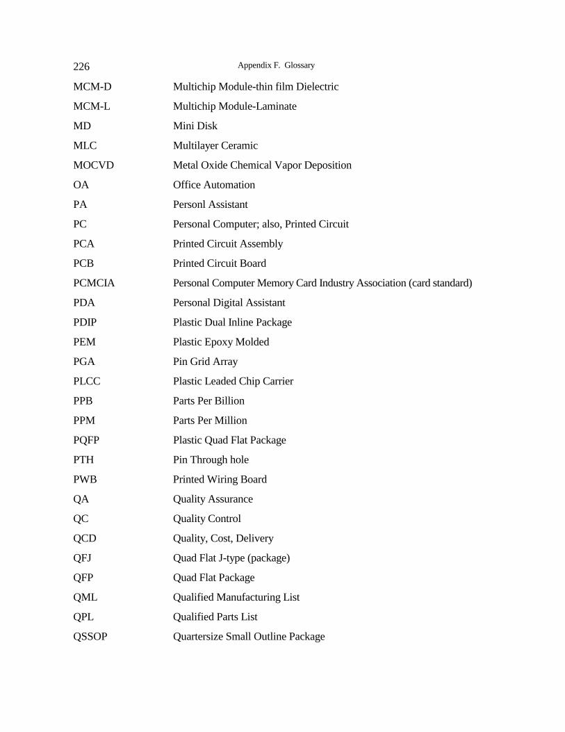
Appendix F. Glossary226
MCM-D Multichip Module-thin film Dielectric
MCM-L Multichip Module-Laminate
MD Mini Disk
MLC Multilayer Ceramic
MOCVD Metal Oxide Chemical Vapor Deposition
OA Office Automation
PA Personl Assistant
PC Personal Computer; also, Printed Circuit
PCA Printed Circuit Assembly
PCB Printed Circuit Board
PCMCIA Personal Computer Memory Card Industry Association (card standard)
PDA Personal Digital Assistant
PDIP Plastic Dual Inline Package
PEM Plastic Epoxy Molded
PGA Pin Grid Array
PLCC Plastic Leaded Chip Carrier
PPB Parts Per Billion
PPM Parts Per Million
PQFP Plastic Quad Flat Package
PTH Pin Through hole
PWB Printed Wiring Board
QA Quality Assurance
QC Quality Control
QCD Quality, Cost, Delivery
QFJ Quad Flat J-type (package)
QFP Quad Flat Package
QML Qualified Manufacturing List
QPL Qualified Parts List
QSSOP Quartersize Small Outline Package
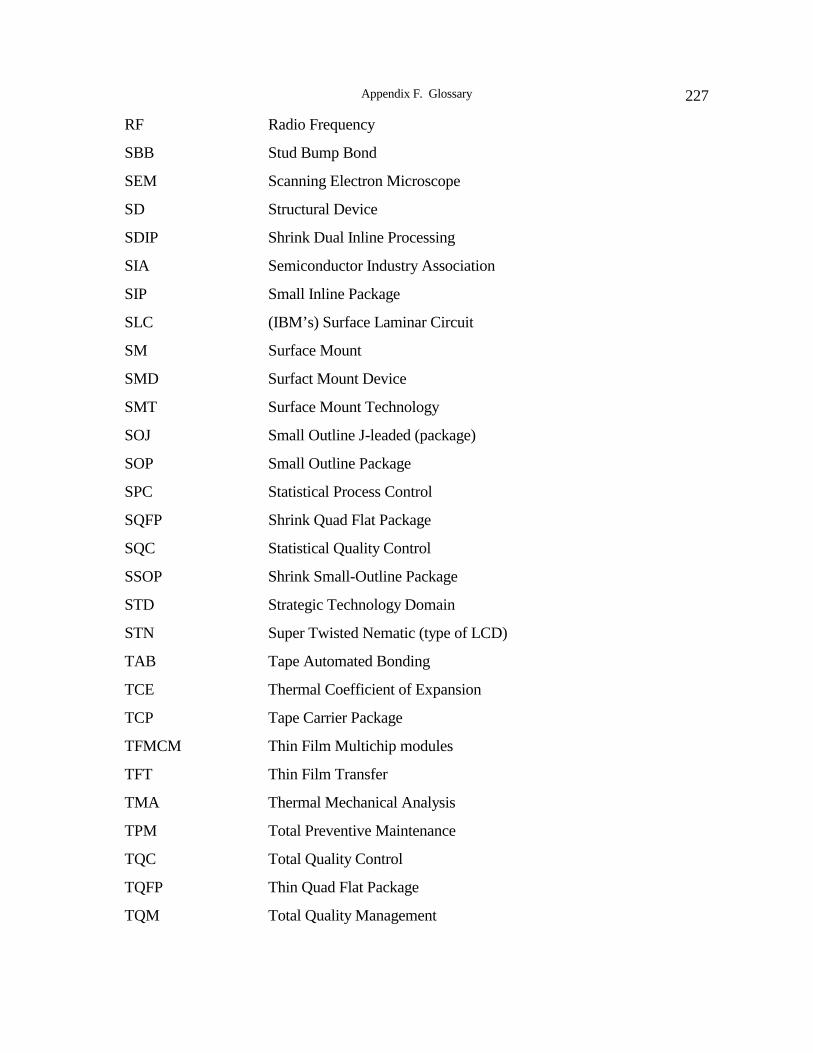
Appendix F. Glossary 227
RF Radio Frequency
SBB Stud Bump Bond
SEM Scanning Electron Microscope
SD Structural Device
SDIP Shrink Dual Inline Processing
SIA Semiconductor Industry Association
SIP Small Inline Package
SLC (IBM’s) Surface Laminar Circuit
SM Surface Mount
SMD Surfact Mount Device
SMT Surface Mount Technology
SOJ Small Outline J-leaded (package)
SOP Small Outline Package
SPC Statistical Process Control
SQFP Shrink Quad Flat Package
SQC Statistical Quality Control
SSOP Shrink Small-Outline Package
STD Strategic Technology Domain
STN Super Twisted Nematic (type of LCD)
TAB Tape Automated Bonding
TCE Thermal Coefficient of Expansion
TCP Tape Carrier Package
TFMCM Thin Film Multichip modules
TFT Thin Film Transfer
TMA Thermal Mechanical Analysis
TPM Total Preventive Maintenance
TQC Total Quality Control
TQFP Thin Quad Flat Package
TQM Total Quality Management

Appendix F. Glossary228
TSOP Thin Small Outline Package
TSSOP Thin Sealed Small Outline Package
TTQFP Thin, Thin Quad Flat Package
ULSI Ultra Large Scale Integration
Vcc Cathode-Cathode Voltage
Vdd Drain Voltage
VCR Video Cassette Recorder
VHS Standard for VCRs initiated by Matsushita
VLSI Very Large Scale Integration
VSOP Very Small Outline Package
VSQFP Very Small Quad Flat Package
VTR Video Tape Recorder
ZD Zero Defects

ISBN 1-883712-37-8
Related Documents